embedded abstract the speed and complexity of integrated
TRANSCRIPT

Optical Networks Magazine July/August 2003 35
Embeddedsignalprocessing usingfree-spaceopticalhypercubeinterconnects
Håkan ForsbergDepartment of Computer Engineering Chalmers University of Technology Göteborg, Sweden
Magnus JonssonBertil SvenssonSchool of Information ScienceComputer and Electrical EngineeringHalmstad UniversityHalmstad, Sweden
ABSTRACTThe speed and complexity of integrated circuits areincreasing rapidly. For instance, today’s mainstreamprocessors have already surpassed gigahertz globalclock frequencies on-chip. As a consequence, manyalgorithms proposed for applications in embeddedsignal-processing (ESP) systems, e.g. radar and sonarsystems, can be implemented with a reasonable number(less than 1000) of processors, at least in terms ofcomputational power. An extreme inter-processor net-work is required, however, to implement those algo-rithms. The demands are such that completely newinterconnection architectures must be considered.
In the search for new architectures, developers ofparallel computer systems can actually take advantageof optical interconnects. The main reason for introduc-ing optics from a system point of view is the strength inusing benefits that enable new architecture concepts,e.g. free-space propagation and easy fan-out, togetherwith benefits that can actually be exploited by simplyreplacing the electrical links with optical ones withoutchanging the architecture, e.g. high bandwidth andcomplete galvanic isolation.
In this paper, we propose a system suitable forembedded signal processing with extreme performancedemands. The system consists of several computationalmodules that work independently and send data simulta-neously in order to achieve high throughput. Each com-putational module is composed of multiple processorsconnected in a hypercube topology to meet scalabilityand high bisection bandwidth requirements. Free-spaceoptical interconnects and planar packaging technologymake it possible to arrange the hypercubes as planeswith an associated three-dimensional communicationspace and to take advantage of many optical properties.For instance, optical fan-out reduces hardware cost.Altogether, this makes the system capable of meetinghigh performance demands in, for example, massivelyparallel signal processing. One 64-channel airborneradar system with nine computational modules and asustained computational speed of more than 1.6 Terafloating point operations per second (TFLOPS) ispresented. The effective inter-module bandwidth in thisconfiguration is 1 024 Gbit/s.
5138455 6/23/03 10:47 AM Page 35
36 Optical Networks Magazine July/August 2003
1 Introduction
A lgorithms recently proposed for applicationsin embedded signal-processing (ESP) systems,e.g. in radar and sonar systems, demand sus-
tained performance in the range of 1 GFLOPS to 50TFLOPS [1]. As a consequence, several processors mustwork together, thus increasing inter-processor communi-cation. Moreover, the data transfer time increases quicklyif an incorrect network topology is chosen, especially insystems with frequent use of all-to-all communicationstructures. The choice of a scalable high-speed network istherefore essential. Other requirements that must befulfilled in ESP systems are real-time processing, low powerconsumption, small physical size, and multimode oper-ation. New parallel computer architectures are necessary tobe able to cope with all these constraints at the same time.
Several parallel and distributed computer systems ofthis kind for embedded real-time applications have beenproposed in the literature, including systems that makeuse of fiber optics in the interconnection network inorder to achieve high bandwidth. See, for instance,Jonsson [3,15]. However, to make the best use of opticsin interprocessing computing systems, all properties ofoptics and optoelectronics must be taken into consider-ation. Among these properties is the ability to communi-cate in free-space in all spatial dimensions as well as,e.g., high fan-out [5].
In fact, a careful evaluation of optics in general showsthat both properties that enable new architecture conceptsand properties that can be exploited without changing thearchitecture increase system performance. In other words,optics not only provides, e.g., higher bandwidth andcomplete galvanic isolation, it also provides a new designspace. This means in reality that optical technologies canimprove some important properties of ESP systems. Forinstance, optics can reduce the physical size and improvethe bandwidth over the cross section that divides a net-work into two halves, usually referred to as the bisectionbandwidth (BB) [4]. High BB reduces the time it takes toredistribute data between computational modules thatprocess information in different dimensions. Thisreduction of time is very important in ESP systems [4].
It has furthermore been shown that optical free-space interconnected 3D systems (systems using all threespatial dimensions for communication), with globallyand regularly interconnected nodes arrayed on planes, arebest suited for parallel computer architectures using optics[7-9]. Folding optically connected 3D systems into planesalso offers precise alignment, mechanical robustness andtemperature stability at a relatively low cost [10].
In this paper, we propose a system consisting ofseveral clusters of free-space optically interconnectedprocessing elements. The clusters are linked together in apipeline fashion to attain high throughput and to meetthe pipelined data flow nature of ESP systems. Theprocessing elements within a cluster are globally and
regularly connected in a binary hypercube topology andare finally transformed into a plane. Note, however, thatthe use of optics does not allow one to collapse higherdimensional graphs to lower dimensional graphs, sinceeven free-space optics requires a minimum finite cross-sectional area. What occurs is that this cross-sectionalarea is sometimes so small that it no longer limits theimplementation, and other factors such as the size of theelements then become limiting factors.
Other networks that have employed the positivefeatures of the hypercube in combination with opticsare, e.g., the Spanning Multichannel Linked Hypercube(SMLH) network [18], the Optical Transpose Intercon-nection System (OTIS) hypercube [19] and the Global-Local Optical Reconfigurable Interconnect (GLORI)network [20].
Our new hardware architecture is evaluated with a64-channel airborne space-time adaptive processing(STAP) radar application. The sustained computationalload is more than 1.6 TFLOPS. As a consequence,several hundreds of processors must be used to reducethe per-processor load. In addition, certain all-to-allcommunication structures must also be used in the signalprocessing chain. This altogether evaluates the perform-ance of the inter-processor communication network inthe new architecture.
Figure 1 depicts an example of the proposed systemarchitecture. Note, however, that the intra-cluster hyper-cube formation is not shown here but later in the text.
The paper is organized as follows. Section 2 introducesthe binary hypercube topology and explains how someimportant all-to-all communication can be implementedon it. In Section 3, we describe how it is possible to mergeinterconnection topologies, including the hypercube, intooptical planes. In Section 4, we show how it is possible tomassively interconnect these optical planes using free-spaceoptics and describe the advantages of doing so. The casestudy discussed in Section 5 demonstrates the power ofusing pipelined optical hypercubes in embedded signalprocessing systems. The paper is concluded in Section 6.
2 HypercubesThe binary hypercube (hereafter called simply the
hypercube) is a flexible topology with many attractivefeatures. For instance, several well-known topologies, suchas meshes, butterflies and shuffle-exchange networks, canbe embedded into it [12]. Rings with an even number ofnodes and certain balanced trees can also be embedded [2].Another feature that makes the hypercube attractive is thatthe bisection bandwidth (BB) scales linearly with the num-ber of processors, and thus higher dimensions lead to veryhigh BB. High BB, as indicated in the introduction, is ofgreat importance in ESP systems.
Geometrically, a hypercube can be defined recursivelyas follows: The zero-dimensional hypercube is a singleprocessor. An n-dimensional hypercube with N � 2n PEs
5138455 6/23/03 10:47 AM Page 36

Optical Networks Magazine July/August 2003 37
Figure 1: Several 6D hypercubes transformed into planes and massively interconnected – an example of theproposed system architecture.
Figure 2: a) 3D hypercube. b) 4D hypercube built of two 3D hyper-cubes. c) 6D hypercube built of two 5D hypercubes, which in turnare built of 4D hypercubes.
is built of two hypercubes with 2n�1 PEs, where all the PEsin one half are connected to the corresponding PEs in theother half. See Figure 2, which shows a six-dimensionalhypercube (Figure 2c). This hypercube is built of two 5Dhypercubes, which in turn are built of 4D hypercubes(Figure 2b). The 4D hypercube is further subdivided into3D hypercubes (Figure 2a). Note that the thick lines inFigure 2c consist of eight interconnections each.
A disadvantage of the hypercube is its complexity. Itrequires more and longer wires than the mesh, since notonly the nearest physical neighbors are connected to eachother if the dimension is greater than three, i.e. moredimensions than in physical space [13]. The fact is thatthe amount of electrical wires already required (ofdifferent lengths) in a relatively small hypercube will beenormous. Consider, for instance, an implementation ofa 6D hypercube on a printed circuit board, where thetransfer rate of a unidirectional channel between twoprocessing elements must be in the order of 10 Gbit/s.This implementation requires 12 288 electrical wires ofdifferent lengths, each clocked with a frequency of 312.5MHz (assuming 32-bit wide channels). Since the wiresare of course not allowed to cross each other physically,many layers will be required.
2.1 Communication in hypercubesHypercubes can be used to implement several
algorithms requiring all-to-all communication, e.g. matrixtransposition, vector reduction, and sorting [13]. It is alsoeasy to implement broadcasting in this architecture [6].Two of the global communication structures, corner
5138455 6/23/03 10:47 AM Page 37

38 Optical Networks Magazine July/August 2003
Figure 3: The corner turning process, i.e. the process of redistributing data between pipeline stages thatcompute in different dimensions.
turning and broadcasting, are of specific importance inembedded signal processing, and we thus discuss them indetail here. (Note that the corner turn algorithm is thesame as a matrix transposition from a mathematical pointof view [4].)• Corner TurningIn corner turning, all nodes send a unique data set to allother nodes. Corner turning is used to efficiently redis-tribute data between pipeline stages that process informa-tion in different dimensions. The following example isgiven to illustrate this:
Assume that we have collected 640 samples in totalfrom eight radar channels (RCs), i.e. 80 samples perchannel. Further, assume that these samples are distri-buted channel-wise over eight processing elements(marked 1-8 in Figure 3). Samples from RC 1 (labeledin Figure 3a) are located in processing element (PE) 1,samples from RC 2 are located in PE 2 etc. In the sub-sequent calculation step (the next pipeline stage), sam-ples 1-10 from all RCs must be processed in PE 1,samples 11-20 from all RCs must be processed in PE 2etc. This means that samples 1-10 from PE 2-8 mustbe redistributed to PE 1, samples 11-20 from PE 1 andPE 3-8 must be redistributed to PE 2 etc. The final re-sult is shown in Figure 3b. Here, one can see that theoriginal data from PE 1 has been scattered over all PEs.The same thing has occurred for all other PEs’ originaldata. This process (the process that takes place betweenFigure 3a and 3b) is called corner turning.One way to efficiently implement corner turning
in the hypercube is to use the hypercube transposealgorithm described by Foster [13]. This algorithm isparticularly good when transfer costs are low and messagestart-ups are expensive [13]. Therefore, optical intercon-nects with their slightly higher start-up cost and highbandwidth typically match the transpose algorithmbehavior better than pure electrical wires. Furthermore,the hypercube transpose algorithm, as well as the broad-casting algorithm described below, only transfer data insuch way that cost-saving optical beam splitters can beused in the interconnection network.
In the hypercube transpose algorithm, half of thechunk of data to be redistributed is exchanged in everydimension. Assume that Dsize is the total size of the chunkof data in number of bits, P is the number of processorsin the hypercube and Rlink,eff is the efficient transfer ratein bits per second of a single link in one direction whenoverhead is excluded, e.g. message start-up time. Then, afull corner turn takes:
(1)
seconds. Note that log2(P) corresponds to the number ofdimensions in the hypercube and that product PRlink,eff
corresponds to the bisection bandwidth (BB). Thus,the reorganization time is proportional to the productof the data chunk size and the cube dimension divided bythe BB.
Using this one-dimension-at-a-time proceduremeans that we can make use of cost-saving single ports,i.e. we use optical beam splitters to reduce the number oftransmitters. Note also that beam splitters allow eachnode to transmit the same data to more than one neigh-bor at the same time. This is an extra feature compared togenuine single-port communication, where a node canonly send and receive on one of its ports at the sametime. On the other hand, transmitting the same data setto more than one node is the exact opposite to cornerturning, where each node sends a unique data set to allother nodes.• BroadcastingIn broadcasting, all nodes need to copy information fromthemselves to all other nodes or a subset thereof. Broad-casting can, for instance, be used in the constant falsealarm ratio (CFAR) stage in certain radar algorithms [5].CFAR is however not considered in this article.
As in the transpose algorithm described above forhypercubes with one-port communication, the datatransfer time for broadcasting is minimized if onedimension is routed at a time. Using this principle, each
12
Dsize log2(P )
PRlink,eff
5138455 6/23/03 10:47 AM Page 38

Optical Networks Magazine July/August 2003 39
Figure 4: Topological and physical view over four PEs in a 3D hy-percube, where the black PE sends data to its three neighbors.
node copies its own amount, M, of data to its firstneighbor (along the first dimension), and simultaneouslyreceives the same amount of data from the same neighbor.The next time, each node copies its own data, andthe data just received from the first neighbor, to thesecond neighbor (along the second dimension), andsimultaneously receives the same amount (i.e. 2M ) ofdata. This procedure is repeated over all dimensions inthe hypercube. Thus each node has to send and receivethe following amount of data:
(2)
where M is the data size (in number of bits) in each nodethat must be copied to all other nodes in the hypercubeand P is the number of processors (nodes). Again, assum-ing that each node has an efficient transfer rate of Rlink,eff
bits per second, broadcasting will take:
(3)
seconds. Note, however, that this expression is validonly if we consider the nodes as single port. In reality, asdescribed above, using optical technology, a copy ofdata from one node can actually be distributed to alllog2(P) neighbors at the same time and each node can infact receive data from all its neighbors at the same time.Of course, this is true only if (i) we are sure that wedo not exceed the optical fan-out limitation of thegiven technology (here, planar free-space optics), (ii) thereceivers are capable of detecting the weaker signals thatresult from the optical beam splitting and (iii) thereceiving nodes are capable of processing multiple infor-mation flows at the same time at the given speed. If allthis holds, the time it takes to broadcast data can bereduced to:
(4)
seconds. To illustrate this, assume that, in a first phase, asingle node receives data from all its log2(P) neighborssimultaneously. Then, in a second phase, the same nodereceives data originating from its neighbors’ neighbors,i.e. the data that were received by the neighbors in thefirst phase. The data transfer is then completed when thenode has received data from all (P-1) nodes. Note, how-ever, that, at the most, log2(P) neighbors, i.e. the numberof physical links, can deliver data at the same time to thesame node.
To conclude, it seems that the hypercube topologywith its high bisection bandwidth is a good candidate for
l (P � 1)log2(P)
mMRlink,eff
(P � 1)MRlink,eff
a log2(P)�1
i �02iM � (P � 1)M
ESP systems that frequently perform corner turning. Onthe other hand, the hypercube is still afflicted with itshigh interconnection complexity. However, restrictingthe nodes to only sending data with one transmitter eachcan reduce this complexity. In addition, if optical beamsplitters and multiple receivers are used together with sin-gle transmitters, the broadcast capabilities of the networkcan be enhanced. Finally, as will be shown in next section,free-space optics and optical planar packaging technologyeven further reduce the interconnection complexity inhypercubes.
3 Hypercubes in Planar Free-Space OpticsThere are many reasons to fold optically intercon-
nected 3D systems into planes. One reason, as will bedemonstrated in this section, is that complicated networktopologies can be transformed into these planes of nodeswith associated three-dimensional communication space.(Remember from the introduction that optics does notcollapse higher dimensional graphs to lower, but reducesthe cross-sectional area to a size and form where it nolonger limits the implementation.) Other reasons to foldoptically interconnected systems into planes are precisealignment, mechanical robustness and the ease of cool-ing, testing and repairing the optoelectronic and elec-tronic circuits attached to the substrates [10,11].
In free-space optical planar technology, waveguidesare made of glass or transparent semiconductor-basedsubstrates. These substrates serve as a light travelingmedium as well as a motherboard for surface mountedoptoelectronic and electronic chips [11]. Micro-opticalelements such as beam splitters and microlenses can alsobe attached to both sides of the substrate. To be able toenclose the optical beams in the light traveling medium,the surfaces are covered with a reflective structure. Thebeams will hence “bounce” on the surface.
In the following three steps, 1-3, and Figures, 4-6,we show how a 3D hypercube topology is merged into
5138455 6/23/03 10:47 AM Page 39

40 Optical Networks Magazine July/August 2003
Figure 6: All transmitters and receivers in a row form a 3D hypercube.
a free-space optical plane. In step 4 and Figure 7, we showhow two 3D hypercubes can be combined into a 4Dhypercube. In step 5 and Figure 8, we show how a com-plete 6D hypercube is merged into a free-space opticalplane. Finally, in step 6 and Figure 9, we show how beamsplitters can be used to reduce the number of transmittersor to enhance the interconnection network.
Before we start with step one, however, it must beclarified that it is possible to implement higher dimen-sional hypercubes (higher than 6D) on a single substratein the same way as shown below (provided that it is phys-ically possible). The choice of a 6D hypercube is only forthe purpose of illustration. The placement of the process-ing elements is also chosen to be as illustrative as possibleand is thus not to be considered as the only one. Finally,many other topologies can be merged in the same way asthe hypercube. Observe, however, that rings, meshes,butterflies and shuffle-exchange networks are automati-cally merged into the substrate when the hypercube ismerged, since these topologies are by default embeddedinto the hypercube. See Section 2.• Step 1: Transmitters
In a 3D hypercube, each processing element has threeneighbors. In Figure 4, it is shown, both topologicallyand physically, how one PE, colored black, sends datato its three neighbors.
• Step 2: ReceiversIn the same way, a PE must be able to receive data fromits three neighbors, see Figure 5.
• Step 3: Complete 3D hypercubesIn Figure 6, all transmitters and receivers in one rowhave been added. This corresponds topologically to a3D hypercube.
• Step 4: 4D hypercubesTo create a 4D hypercube, we make use of two rows. SeeFigure 7. In the topological view in this figure, all PEs inthe left 3D hypercube are connected to the nodes in theright hypercube. In the physical view, this corresponds
Figure 7: Two 3D hypercubes (rows) form a 4D hypercube.
Figure 5: Topological and physical view of four PEs in a 3Dhypercube, where the black PE receives data from its threeneighbors.
5138455 6/23/03 10:47 AM Page 40

Optical Networks Magazine July/August 2003 41
Figure 8: The whole computational module – a 6D hypercube.
Figure 9: a) Beam splitters are used to reduce the number oftransmitters in a node (here by a factor of three). b) Beam splittersare used to increase the flexibility and multicast capacity in thenetwork at the expense of more receivers but without additionaltransmitters.
to connections between each PE, and the correspondingone in the other. This is illustrated with a line on top ofthe substrate.
• Step 5: 6D hypercubesA 6D hypercube makes full use of both horizontal andvertical space on a substrate (at least in this example),see Figure 8. The physical layout corresponds to a fullcomputational module.
As mentioned earlier, micro-optical elements can beattached to the substrate. One such element is the opticalbeam splitter. If we use beam splitters in the hypercube, itis actually possible to reduce the number of transmittersby a factor equal to the number of dimensions withoutdestroying the topology. As an example, if we want to im-plement a 6D hypercube that originally has 384 (6 � 64)transmitters, it is sufficient to use 64 if we take full ad-vantage of the beam splitters. The only restriction is thatwe must use some kind of channel time-sharing whendifferent data must be sent to different neighbors at thesame time, since only a single transmitter is available ineach node. Figure 9 shows how optical beam splitterscan be used to reduce the number of transmitters or toenhance the interconnection network.
Furthermore, if we use the hypercube transposealgorithm described by Foster [13] to perform cornerturning, we will not lose any performance at all, even ifwe reduce the number of transmitters by a factor of six ina 6D hypercube as compared to a system without beamsplitters. The trick in this algorithm is that data areexchanged in only one dimension at a time. Note,however, that the hypercube transpose algorithm sendsmore data and fewer messages in total, as compared to asimpler transposition algorithm also described by Foster[13]. Therefore, as mentioned above, the hypercube
transpose algorithm is preferable when transfer costs arelow and message start-ups are expensive, e.g. in opticalinterconnection networks.
Last but not least, other sophisticated topologies canbe created with beam splitters, although these will not betreated here.• Step 6: Reduction of transmitters
As explained above, we will not lose any performance atall when we perform corner turning in the hypercube
5138455 6/23/03 10:47 AM Page 41

42 Optical Networks Magazine July/August 2003
Figure 10: a) Inter-plane transmitting mechanism. b) Inter-planereceiving mechanism.
with fewer transmitters and with the help of beam split-ters. As a consequence, we will use the beam splittersdepicted in Figure 9a above. Note, however, that wesplit the light beam in both the horizontal and verticaldirections, and thus maximally reduce the number oftransmitters, i.e. by a factor of six.
In the same way as we investigated optical fan-out,we can analyze optical fan-in. In Figure 5, for instance, itis fully possible to use a single receiver for all beams. Inthat case, we must use some kind of time division multi-ple access to avoid data collisions and to synchronize allprocessing elements in the hypercube. However, withoptical planar packaging technology, a synchronizationclock channel is relatively easy to implement. Jahns [10],for instance, has described a 1-to-64 signal distributionsuitable for, e.g., clock sharing, with planar packagingtechnology. However, since optical fan-in complicatesour hypercubes with synchronization channels, we willput this issue aside.
4 Pipelined Systems of HypercubesIf the required load exceeds the computational
power in one module, several modules must co-operate.To make these modules work together efficiently, mas-sively parallel interconnections are necessary. One way tointerconnect several modules is to place them in succes-sion, as in Figure 1. The possible drawback of thisplacement is that each plane can only send data forwardand backward to the subsequent and the previous mod-ule, respectively. However, this arrangement suits thepipelined computational nature in most ESP systems andis therefore a good choice for such applications.
To make the inter-module communication work, wehave to open up the substrates, i.e. let the lightbeams propagate via a lens from one module to the next.Figure 10 shows this inter-plane transmission. Specifi-cally, Figure 10a shows the light propagation from onemodule to the next via a bottom surface lens. Figure 10bshows the top surface receiver. Note that it is possible touse a dedicated receiver module in Figure 10b instead ofusing the top surface of the computational unit as shown.
4.1 7D hypercube—two planar arraysThe section above showed how the substrate is
opened in order to connect computational modules.This procedure showed only how the modules were con-nected in one direction, however, i.e. one module couldonly receive from the previous module and send data tothe next one. By allowing communication in both direc-tions, i.e. letting a module be able to send and receivedata both forward and backward, a 7D hypercube isactually formed by two planar arrays, see Figure 11.If more than two planes form an extended computa-tional module, the pure hypercube topology will not bepreserved since only adjacent planes can communicate
with each other. This, however, is not a limitation in atypical signal processing system owing to the pipelinednature of the data flow.
4.2 Software scalabilityIf only one mode of operation is needed in the
system, we can create a streamed architecture for thatpurpose. However, since it is very important in manyESP applications to change the mode of operation on thesame system as needed in the application, we would liketo have an architecture capable of multimode operations.Thus, different clusters of computational units must becapable of working together in different ways.
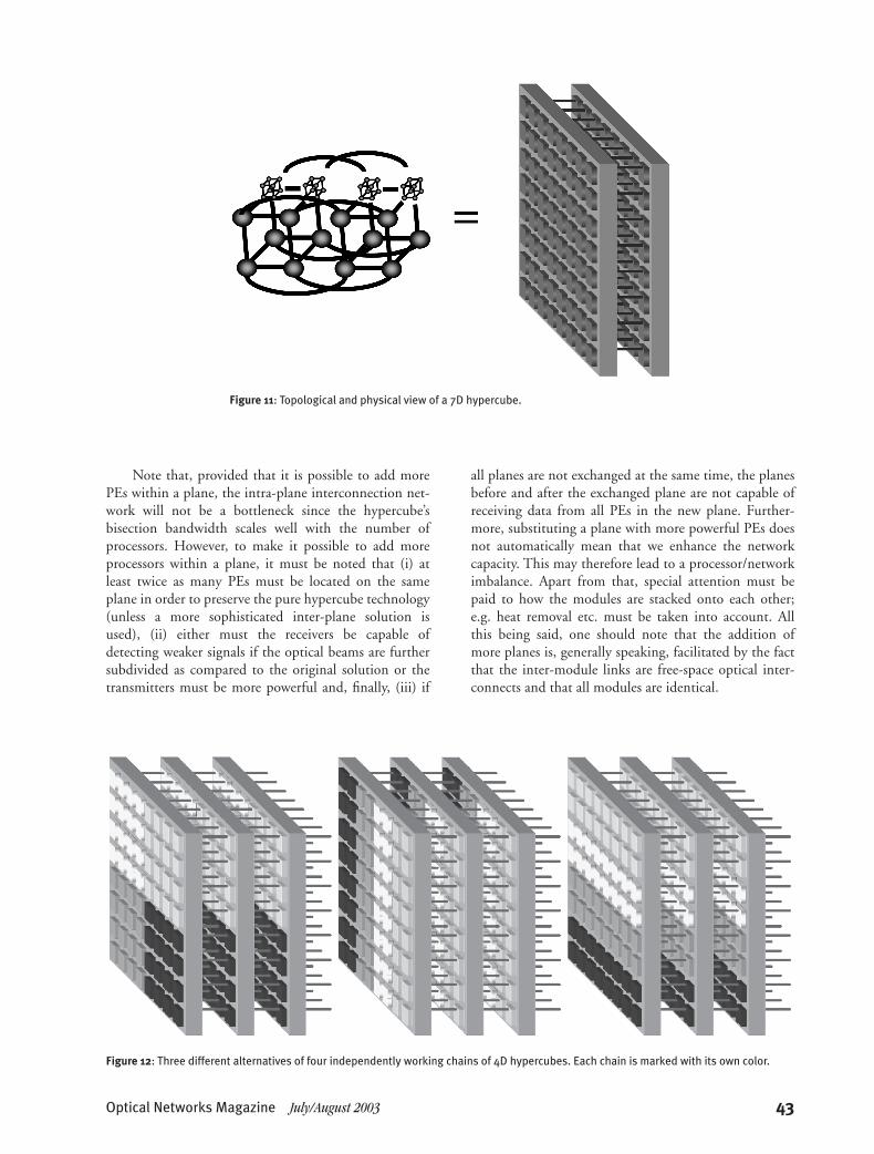
The pipelined system described in this paper hasvery good potential for mapping of different algorithmsin various ways. In fact, the system can be partitioned inall three spatial dimensions. An example of this is shownin Figure 12. In this picture, three different alternativesshow exactly the same thing, namely, four different tasksmapped on four smaller systems of pipelined 4D hyper-cubes. It is also possible to create 5D hypercubes insideeach of these four smaller systems by connecting two 4Dhypercubes in different planes.
4.3 Hardware scalabilityTo be able to increase system performance in the
future, hardware scalability is of great importance. Higherperformance can be achieved in the proposed system by:a) adding more planar arrays in the chain,b) adding more PEs within a plane by denser packag-
ing orc) substituting a plane with more powerful PEs.
5138455 6/23/03 10:47 AM Page 42
Optical Networks Magazine July/August 2003 43
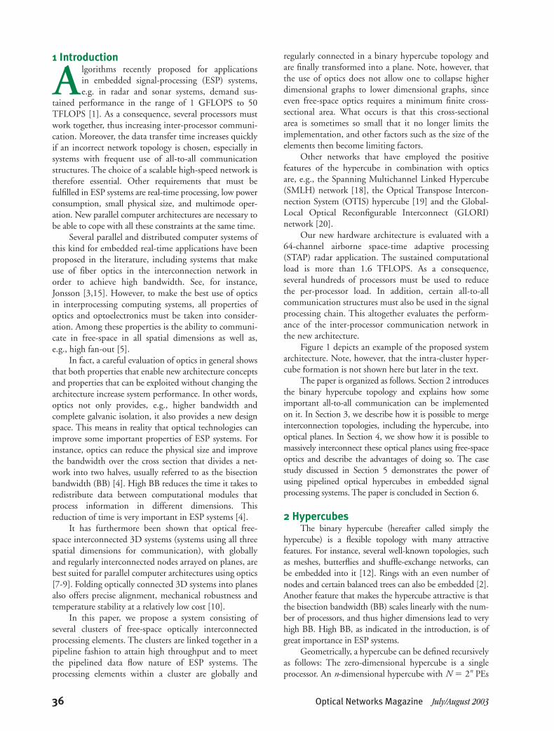
Figure 11: Topological and physical view of a 7D hypercube.
Figure 12: Three different alternatives of four independently working chains of 4D hypercubes. Each chain is marked with its own color.
Note that, provided that it is possible to add morePEs within a plane, the intra-plane interconnection net-work will not be a bottleneck since the hypercube’sbisection bandwidth scales well with the number ofprocessors. However, to make it possible to add moreprocessors within a plane, it must be noted that (i) atleast twice as many PEs must be located on the sameplane in order to preserve the pure hypercube technology(unless a more sophisticated inter-plane solution isused), (ii) either must the receivers be capable ofdetecting weaker signals if the optical beams are furthersubdivided as compared to the original solution or thetransmitters must be more powerful and, finally, (iii) if
all planes are not exchanged at the same time, the planesbefore and after the exchanged plane are not capable ofreceiving data from all PEs in the new plane. Further-more, substituting a plane with more powerful PEs doesnot automatically mean that we enhance the networkcapacity. This may therefore lead to a processor/networkimbalance. Apart from that, special attention must bepaid to how the modules are stacked onto each other;e.g. heat removal etc. must be taken into account. Allthis being said, one should note that the addition ofmore planes is, generally speaking, facilitated by the factthat the inter-module links are free-space optical inter-connects and that all modules are identical.
5138455 6/23/03 10:47 AM Page 43
44 Optical Networks Magazine July/August 2003
5 Case StudyAn airborne radar signal processing unit for non-movablephased steered antennas is chosen as a case study. In thistype of radar, it is possible to make adaptive beam form-ing in the signal processing chain and thus significantlyimprove the functional performance of the system. Thisprocess is often called space-time adaptive processing(STAP).
STAP requires a huge amount of calculations andputs high demands on inter-processor communication.Therefore, the new architecture must be capable ofhandling both high system load and high-volume inter-processor data transfers.
In this study, a single processing element is assumed tohave a sustained floating point capacity of approximately 3GFLOPS when all inter-processor data communication isexcluded. In addition, for simplicity, no overlap betweencomputation and communication is assumed.
5.1 The airborne STAP-radar systemSTAP is an innovative tool for use with coherent
phased array radar (and sonar) systems whenever the sig-nals received are functions of both space and time [14].STAP can, for instance, be used in airborne radar sys-tems to support clutter and interference cancellation[17]. However, the full STAP algorithm is of little valuein most applications since the computational workload istoo high and it suffers from weak convergence [14].Some kind of load-reducing and fast convergent algo-rithm is thus used. Examples are the nth order Doppler-factored STAP, the medium (1st order) real-time STAPand the hard (3rd order) real-time STAP, all described byCain et al. [17]. This study uses the same type of real-time STAP, although the computational load is increasedmany times. The reasons for this are, besides the higherorder STAP (5th order), also the increase in input pro-cessing channels and the higher sampling rate etc.
The following system parameters are assumed for theairborne radar system:• 64 processing channels (L)• 5th order Doppler-factored STAP (Q)• 32.25 ms integration interval (INTI) (�)
• 960 samples (range bins) (Nd) per pulse after decima-tion with a factor of four
• 64 pulses per INTI and channel (Cp)• 8 Gbit/s efficient data transfer rate of a single link in
one direction (Rlink,eff)Because of the real-time nature of the system, a
solution must have low computational latency. We thusput up a latency requirement slightly less than 100 ms,i.e. a maximum time of 3� to perform all calculations inthe STAP chain from the input stage to the final stage.Note also that it is important to use as much time aspossible without violating the latency requirement sincethe maximum latency determines the number of opera-tions performed per time unit.
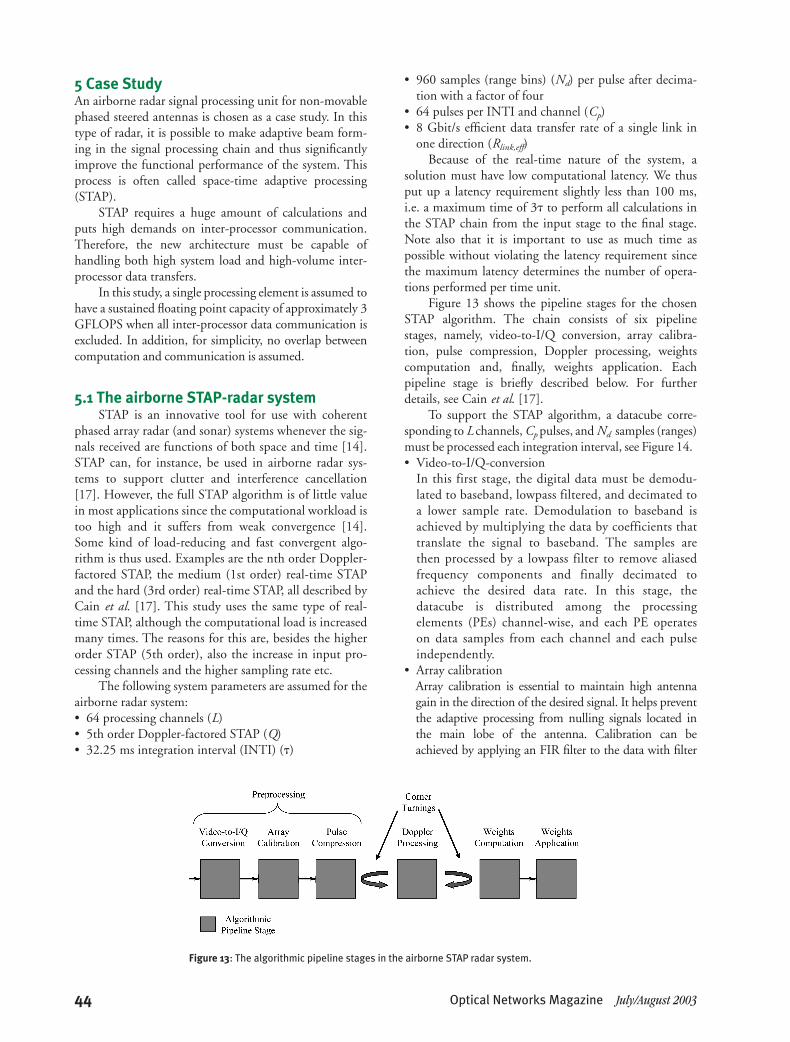
Figure 13 shows the pipeline stages for the chosenSTAP algorithm. The chain consists of six pipelinestages, namely, video-to-I/Q conversion, array calibra-tion, pulse compression, Doppler processing, weightscomputation and, finally, weights application. Eachpipeline stage is briefly described below. For furtherdetails, see Cain et al. [17].
To support the STAP algorithm, a datacube corre-sponding to L channels, Cp pulses, and Nd samples (ranges)must be processed each integration interval, see Figure 14.• Video-to-I/Q-conversion
In this first stage, the digital data must be demodu-lated to baseband, lowpass filtered, and decimated toa lower sample rate. Demodulation to baseband isachieved by multiplying the data by coefficients thattranslate the signal to baseband. The samples arethen processed by a lowpass filter to remove aliasedfrequency components and finally decimated toachieve the desired data rate. In this stage, thedatacube is distributed among the processingelements (PEs) channel-wise, and each PE operateson data samples from each channel and each pulseindependently.
• Array calibrationArray calibration is essential to maintain high antennagain in the direction of the desired signal. It helps preventthe adaptive processing from nulling signals located inthe main lobe of the antenna. Calibration can beachieved by applying an FIR filter to the data with filter
Figure 13: The algorithmic pipeline stages in the airborne STAP radar system.
5138455 6/23/03 10:47 AM Page 44

Optical Networks Magazine July/August 2003 45
Figure 14: The three-dimensional datacube that must beprocessed every integration interval.
Figure 15: Distribution of QR decompositions in the datacube. The dark block correspondsto a matrix used in one QR decomposition.
coefficients designed to equalize the antenna response.The PEs work with the output data from the previousstage and process each channel and pulse independently.Therefore, no data need to be redistributed.
• Pulse compressionTo achieve high signal energy and improved detectionperformance, pulse compression is applied to thepulses. Pulse compression is achieved by applying anFIR filter to the data with filter coefficients matched tothe received signal waveform. As in the two previousstages, each PE operates on data samples from eachchannel and each pulse independently. Therefore, nodata need to be redistributed.
• Doppler processingDoppler processing is a key component in all Doppler-factored STAP algorithms. In this stage, multiplepulses are processed to separate signals based upontheir Doppler frequency. Doppler processing is imple-mented by applying a discrete Fourier transform acrossmultiple pulses of the preprocessed data for a givenrange and cell. Hence, we need to perform a cornerturning before we start to compute in this stage. This isillustrated in Figure 13.
• Weights computationIn this stage, adaptive weights are calculated from thedata received from multiple channels to control the spa-tial response of the system. The algorithm computes a
set of adaptive weights, using a data domain approachthat involves a matrix factorization called QR decom-position. Each PE in this stage needs data from allchannels and multiple range samples but only from onepulse at a time (see Figure 15 and the following text).This means, again, that we need to perform a cornerturning before this stage.
• Weights applicationIn this final stage, the whole concept of STAP comesinto play. The weights that have been calculated in theprevious stage are applied in the system to allow the al-gorithm to adjust its temporal and spatial response inorder to null clutter returns and interference and toadapt to changes in the signal environment. No redis-tribution is needed before this stage.
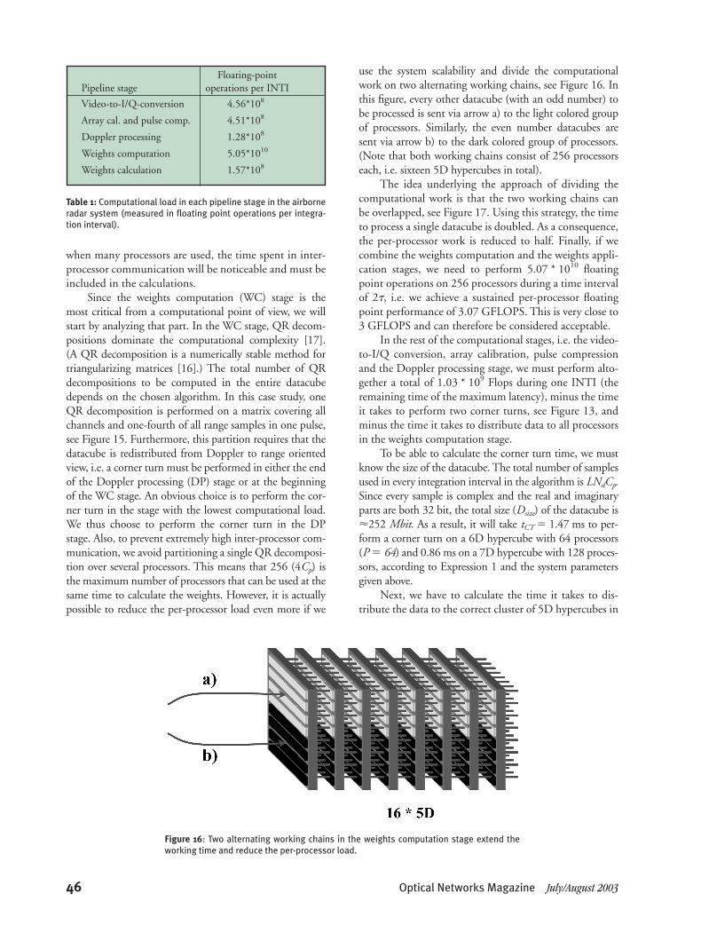
Table 1 shows the computational load in each pipelinestage. The load is measured in floating point opera-tions per integration interval (INTI) (and not per second).Note that all floating point calculations are derived fromequations in Cain et al. [17]. Note also that the arraycalibration and the pulse compression stages are combinedin Table 1.
Clearly, the most difficult stage to calculate is theweights computation (a factor of 100 times more calcula-tions than the other stages).
5.2 Hardware architecture analysisLet us assume for a brief moment that we only have
one processor with its own memory. If we perform allcalculations with one processor, we have to perform5.17*1010 floating point operations during one INTI.This corresponds to a sustained performance of morethan 1.6 TFLOPS (Tera floating point operations persecond), and this is too high for a single processor. As aconsequence, we must reduce the per-processor load byusing several processors and by using as much time aspossible without violating the latency requirement. Theextended working time is achieved by pipeliningsome computational parts in the chain. In addition,
5138455 6/23/03 10:47 AM Page 45
46 Optical Networks Magazine July/August 2003
Figure 16: Two alternating working chains in the weights computation stage extend theworking time and reduce the per-processor load.
when many processors are used, the time spent in inter-processor communication will be noticeable and must beincluded in the calculations.
Since the weights computation (WC) stage is themost critical from a computational point of view, we willstart by analyzing that part. In the WC stage, QR decom-positions dominate the computational complexity [17].(A QR decomposition is a numerically stable method fortriangularizing matrices [16].) The total number of QRdecompositions to be computed in the entire datacubedepends on the chosen algorithm. In this case study, oneQR decomposition is performed on a matrix covering allchannels and one-fourth of all range samples in one pulse,see Figure 15. Furthermore, this partition requires that thedatacube is redistributed from Doppler to range orientedview, i.e. a corner turn must be performed in either the endof the Doppler processing (DP) stage or at the beginningof the WC stage. An obvious choice is to perform the cor-ner turn in the stage with the lowest computational load.We thus choose to perform the corner turn in the DPstage. Also, to prevent extremely high inter-processor com-munication, we avoid partitioning a single QR decomposi-tion over several processors. This means that 256 (4Cp) isthe maximum number of processors that can be used at thesame time to calculate the weights. However, it is actuallypossible to reduce the per-processor load even more if we
use the system scalability and divide the computationalwork on two alternating working chains, see Figure 16. Inthis figure, every other datacube (with an odd number) tobe processed is sent via arrow a) to the light colored groupof processors. Similarly, the even number datacubes aresent via arrow b) to the dark colored group of processors.(Note that both working chains consist of 256 processorseach, i.e. sixteen 5D hypercubes in total).
The idea underlying the approach of dividing thecomputational work is that the two working chains canbe overlapped, see Figure 17. Using this strategy, the timeto process a single datacube is doubled. As a consequence,the per-processor work is reduced to half. Finally, if wecombine the weights computation and the weights appli-cation stages, we need to perform 5.07 * 1010 floatingpoint operations on 256 processors during a time intervalof 2�, i.e. we achieve a sustained per-processor floatingpoint performance of 3.07 GFLOPS. This is very close to3 GFLOPS and can therefore be considered acceptable.
In the rest of the computational stages, i.e. the video-to-I/Q conversion, array calibration, pulse compressionand the Doppler processing stage, we must perform alto-gether a total of 1.03 * 109 Flops during one INTI (theremaining time of the maximum latency), minus the timeit takes to perform two corner turns, see Figure 13, andminus the time it takes to distribute data to all processorsin the weights computation stage.
To be able to calculate the corner turn time, we mustknow the size of the datacube. The total number of samplesused in every integration interval in the algorithm is LNdCp.Since every sample is complex and the real and imaginaryparts are both 32 bit, the total size (Dsize) of the datacube is�252 Mbit. As a result, it will take tCT � 1.47 ms to per-form a corner turn on a 6D hypercube with 64 processors(P � 64) and 0.86 ms on a 7D hypercube with 128 proces-sors, according to Expression 1 and the system parametersgiven above.
Next, we have to calculate the time it takes to dis-tribute the data to the correct cluster of 5D hypercubes in
Table 1: Computational load in each pipeline stage in the airborneradar system (measured in floating point operations per integra-tion interval).
Floating-point Pipeline stage operations per INTI
Video-to-I/Q-conversion 4.56*108
Array cal. and pulse comp. 4.51*108
Doppler processing 1.28*108
Weights computation 5.05*1010
Weights calculation 1.57*108
5138455 6/23/03 10:47 AM Page 46
Optical Networks Magazine July/August 2003 47
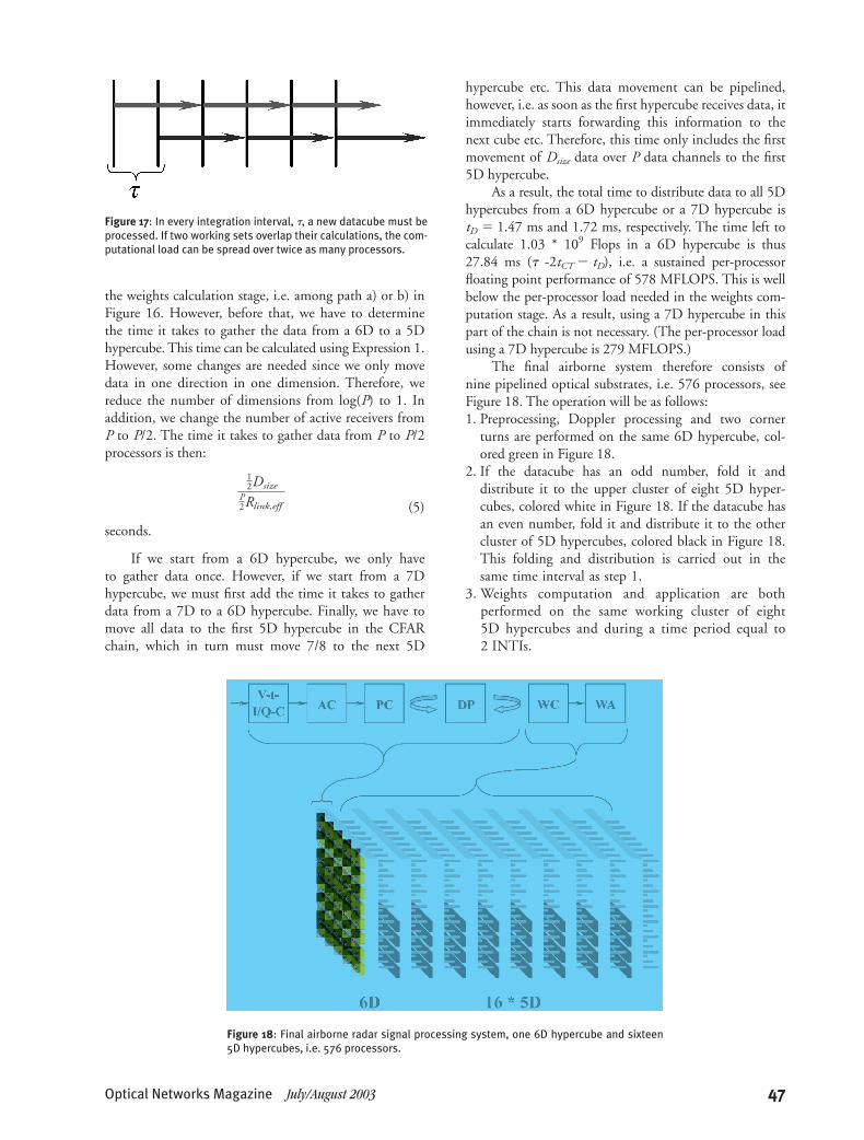
Figure 17: In every integration interval, �, a new datacube must beprocessed. If two working sets overlap their calculations, the com-putational load can be spread over twice as many processors.
Figure 18: Final airborne radar signal processing system, one 6D hypercube and sixteen5D hypercubes, i.e. 576 processors.
the weights calculation stage, i.e. among path a) or b) inFigure 16. However, before that, we have to determinethe time it takes to gather the data from a 6D to a 5Dhypercube. This time can be calculated using Expression 1.However, some changes are needed since we only movedata in one direction in one dimension. Therefore, wereduce the number of dimensions from log(P) to 1. Inaddition, we change the number of active receivers fromP to P/2. The time it takes to gather data from P to P/2processors is then:
(5)
seconds.
If we start from a 6D hypercube, we only haveto gather data once. However, if we start from a 7Dhypercube, we must first add the time it takes to gatherdata from a 7D to a 6D hypercube. Finally, we have tomove all data to the first 5D hypercube in the CFARchain, which in turn must move 7/8 to the next 5D
12Dsize
P2Rlink,eff
hypercube etc. This data movement can be pipelined,however, i.e. as soon as the first hypercube receives data, itimmediately starts forwarding this information to thenext cube etc. Therefore, this time only includes the firstmovement of Dsize data over P data channels to the first5D hypercube.
As a result, the total time to distribute data to all 5Dhypercubes from a 6D hypercube or a 7D hypercube istD � 1.47 ms and 1.72 ms, respectively. The time left tocalculate 1.03 * 109 Flops in a 6D hypercube is thus27.84 ms (� -2tCT � tD), i.e. a sustained per-processorfloating point performance of 578 MFLOPS. This is wellbelow the per-processor load needed in the weights com-putation stage. As a result, using a 7D hypercube in thispart of the chain is not necessary. (The per-processor loadusing a 7D hypercube is 279 MFLOPS.)
The final airborne system therefore consists ofnine pipelined optical substrates, i.e. 576 processors, seeFigure 18. The operation will be as follows:1. Preprocessing, Doppler processing and two corner
turns are performed on the same 6D hypercube, col-ored green in Figure 18.
2. If the datacube has an odd number, fold it anddistribute it to the upper cluster of eight 5D hyper-cubes, colored white in Figure 18. If the datacube hasan even number, fold it and distribute it to the othercluster of 5D hypercubes, colored black in Figure 18.This folding and distribution is carried out in thesame time interval as step 1.
3. Weights computation and application are bothperformed on the same working cluster of eight5D hypercubes and during a time period equal to2 INTIs.
5138455 6/23/03 10:47 AM Page 47

48 Optical Networks Magazine July/August 2003
6 ConclusionsThis paper has presented a powerful system suitable
for embedded signal processing. Several computationalmodules capable of working independently and sendingdata simultaneously are massively interconnected to meethigh throughput demands. The hypercube topologyforms the interconnection network within a computa-tional module. Free-space optical interconnects andplanar packaging technology make it possible to mergethese multi-dimensional hypercubes into optical planes.Beam splitters reduce the number of transmitters andthus also the hardware cost.
An airborne STAP radar application challenged thearchitecture in terms of computational load and inter-processor data transfer. With a sustained per-processor per-formance of slightly more than 3 GFLOPS, a total of 576processors and a bisection bandwidth of more than 1 Tbit/s,the system was capable of meeting all requirements.
It can be noted that solutions that are non-optimal,in the sense that there is no overlap between computa-tion and communication, put higher demands on thearchitecture. However, not putting as great an effortinto optimizing overlap simplifies the software develop-ment, thus increasing engineering efficiency. On theother hand, if more suitable mappings of the algorithmsare developed (at the expense of higher complexity),more powerful systems can be built using this newhardware architecture.
7 AcknowledgmentThis work is financed by Ericsson Microwave
Systems within the Intelligent Antenna Systems Project.
8 References[1] W. Liu and V. K. Prasanna, “Utilizing the power of
high performance computing,” IEEE Signal Process-ing Magazine, vol. 15, no. 5, Sept. 1998, pp. 85100.
[2] D. P. Bertsekas and J. N. Tsitsiklis, Parallel and Dis-tributed Computation: Numerical Methods, Prentice-Hall, inc., Englewood Cliffs, NJ, USA, 1989.
[3] M. Jonsson, High Performance Fiber-OpticInterconnection Networks for Real-Time Comput-ing Systems, Doctoral Thesis, Department ofComputer Engineering, Chalmers University ofTechnology, Göteborg, Sweden, Nov. 1999, ISBN91-7197-852-6. Thesis available at: http://www.hh.se/staff/magnusj/
[4] K. Teitelbaum, “Crossbar tree networks for embed-ded signal processing applications,” Proceedings ofMassively Parallel Processing using Optical Intercon-nections, MPPOI’98, Las Vegas, NV, USA, June15-17, 1998, pp. 200-207.
[5] H. Forsberg, “Parallel computer architectures usingoptical interconnects,” Licentiate Thesis, TechnicalReport no. 379L, Department of Computer
Engineering, Chalmers University of Technology,Göteborg, Sweden, March 2001.
[6] M. D. Grammatikakis, D. F. Hsu, and M. Kraetzl,Parallel System Interconnections and Communica-tions, CRC Press, Boca Raton, Florida, USA, 2001.
[7] H. M. Ozaktas, “Fundamentals of optical intercon-nections – a review,” Proceedings of Massively ParallelProcessing using Optical Interconnections, MPPOI’97,Montreal, Canada, June 22-24, 1997, pp. 184-189.
[8] H. M. Ozaktas, “Toward an optimal foundationarchitecture for optoelectronic computing. Part I.Regularly interconnected device planes,” AppliedOptics, vol. 36, no. 23, Aug. 10, 1997, pp. 5682-5696.
[9] H. M. Ozaktas, “ Toward an optimal foundationarchitecture for optoelectronic computing. Part II.Physical construction and application platforms,”Applied Optics, vol. 36, no. 23, Aug. 10, 1997,pp. 5697-5705.
[10] J. Jahns, “Planar packaging of free-space opticalinterconnections,” Proceedings of the IEEE, vol. 82,no. 11, Nov. 1994, pp. 1623-1631.
[11] J. Jahns, “Integrated free-space optical intercon-nects for chip-to-chip communications,” Proceed-ings of Massively Parallel Processing using OpticalInterconnections, MPPOI’98, Las Vegas, NV, USA,June 15-17, 1998, pp. 20-23.
[12] D. E. Culler, J.P. Singh, with A. Gupta, Parallel Com-puter Architecture: A Hardware/Software Approach,Morgan Kaufmann Publishers, Inc., San Francisco,CA, USA, 1999.
[13] I. Foster, Designing and Building Parallel Programs:Concepts and Tools for Parallel Software Engineering,Addison Wesley Publishing Company, Inc., Read-ing, MA, USA, 1995.
[14] R. Klemm, “Introduction to space-time adaptiveprocessing,” The Institution of Electrical Engineers(IEE), Savoy Place, London WC2R OBL, UK, 1998.
[15] M. Jonsson, “Fiber-optic interconnection networksfor signal processing applications,” 4th Interna-tional Workshop on Embedded HPC Systems andApplications (EHPC’99) held in conjunction with the13th International Parallel Processing Symposium &10th Symposium on Parallel and Distributed Process-ing (IPPS/SPDP ‘99), San Juan, Puerto Rico, Apr.16, 1999. Published in Lecture Notes in ComputerScience, vol. 1586, Springer Verlag, 1999, pp.1374-1385, ISBN 3-540-65831-9.
[16] M. Taveniku and A. Åhlander, “Instruction statis-tics in array signal processing,” Research Report,Centre for Computer Systems Architecture, Halm-stad University, Sweden, 1997.
[17] K. C. Cain, J. A. Torres, and R. T. Williams,“RT_STAP: Real-time space-time adaptive process-ing benchmark,” MITRE Technical Report, TheMITRE Corporation, Center for Air Force C3Systems, Bedford, MA, USA, 1997.
5138455 6/23/03 10:47 AM Page 48

1997 and 1999, respectively. From 1998 to March 2003, he wasAssociate Professor of Data Communication at Halmstad University(acting between 1998 and 2000). Since April 2003, he has beenProfessor of Real-Time Computer Systems at Halmstad University.He has published about 35 scientific papers, most of them in the areaof optical communication and real-time communication. Most ofhis research is targeted for embedded, industrial and parallel anddistributed computing and communication systems. Dr. Jonsson hasserved on the program committees of International Workshop on Op-tical Networks, IEEE International Workshop on Factory Commu-nication Systems, International Conference on Computer Scienceand Informatics, and International Workshop on Embedded/Dis-tributed HPC Systems and Applications.
Bertil [email protected] Svensson received his M.Sc. in Elec-trical Engineering from the University ofLund, Sweden, in 1970 and his Ph.D. inComputer Engineering from the sameUniversity in 1983. He was an AssistantProfessor and Vice President of HalmstadUniversity, Halmstad, Sweden, before he, in 1991, was appointedprofessor of Computer Systems Engineering at Chalmers Universityof Technology in Gothenburg, Sweden. From 1998 he is Professor ofComputer Systems Engineering at Halmstad University andChalmers. He is also Dean of the School of Information Science,Computer and Electrical Engineering at Halmstad University.
Prof. Svensson is research leader of the Laboratory for Com-puting and Communication at Halmstad University. His researchinterests include massively parallel architectures, application-oriented architectures for embedded systems, reconfigurable archi-tectures, and optically interconnected parallel systems.
Optical Networks Magazine July/August 2003 49
[18] A. Louri, B. Weech, and C. Neocleous, “A span-ning multichannel linked hypercube: a graduallyscalable optical interconnection network for mas-sively parallel computing,” IEEE Transactions onParallel and Distributed Systems, vol. 9, no. 5, May1998, pp. 497-512.
[19] F. Zane, P. Marchand, R. Paturi, and S. Esener,“Scalable network architectures using the opticaltranspose interconnection system (OTIS),” Journalof Parallel and Distributed Computing, 60:5, 2000,pp. 521-538.
[20] T. M. Pinkston and J. W. Goodman, “Design of anoptical reconfigurable shared-bus-hypercube inter-connect,” Applied Optics, vol. 33, no. 8, 10 March1994, pp. 1434-1443.
Håkan [email protected]åkan Forsberg received his M.S. degreein computer science and engineering fromLinköping University, Sweden, in 1997,and Licentiate of Technology degree incomputer engineering from ChalmersUniversity of Technology, Gothenburg,Sweden, in 2001. From 1996 to 1998,Mr. Forsberg was an electronic design and research engineer at SaabAvionics AB. Currently, he is with the Department of Computer En-gineering at Chalmers University of Technology. His Ph.D. Studiesare concerned with parallel computer architectures using optical in-terconnects.
Magnus [email protected] Jonsson received his B.S. andM.S. degrees in computer engineeringfrom Halmstad University, Sweden, in1993 and 1994, respectively. He thenobtained the Licentiate of Technology andPh.D. degrees in computer engineeringfrom Chalmers University of Technology, Gothenburg, Sweden, in
5138455 6/23/03 10:47 AM Page 49