risc processor design - welcome to the serc …viren/courses/2010/se273/lecture13.pdfrisc processor...
TRANSCRIPT

RISC Processor DesignSingle Cycle Implementation -
MIPSMIPS
Virendra SinghIndian Institute of Science
Bangalorevirendra@computer [email protected]
Lecture 13
SE-273: Processor Design

Courtesy: Prof. Vishwani Agrawal
Feb 13, 2010 SE-273@SERC 2
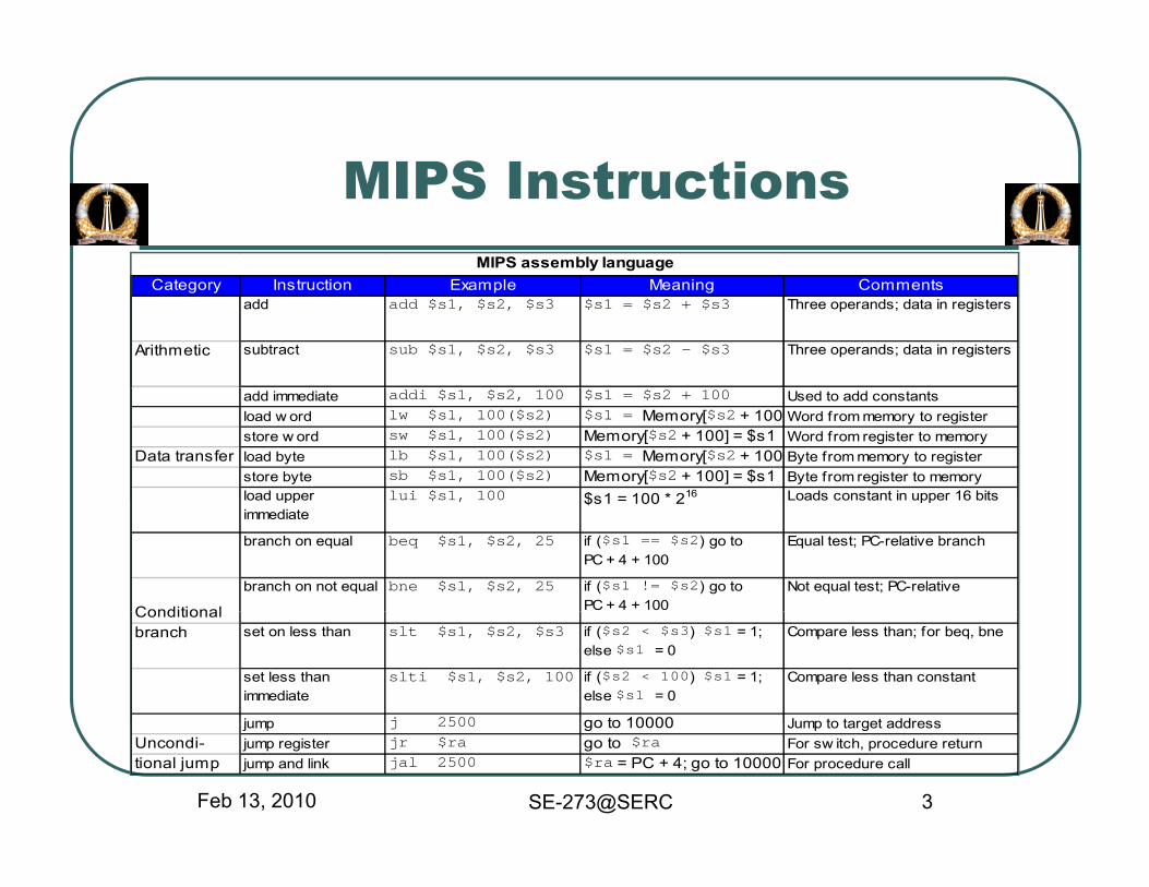
MIPS I t tiMIPS InstructionsMIPS assembly language
Category Instruction Example Meaning Commentsadd add $s1, $s2, $s3 $s1 = $s2 + $s3 Three operands; data in registers
Arithmetic subtract sub $s1, $s2, $s3 $s1 = $s2 - $s3 Three operands; data in registers
add immediate addi $s1, $s2, 100 $s1 = $s2 + 100 Used to add constantsload w ord lw $s1, 100($s2) $s1 = Memory[$s2 + 100 Word from memory to registerstore w ord sw $s1, 100($s2) Memory[$s2 + 100] = $s1 Word from register to memory
Data transfer load byte lb $s1, 100($s2) $s1 = Memory[$s2 + 100 Byte from memory to registerstore byte sb $s1, 100($s2) Memory[$s2 + 100] = $s1 Byte from register to memoryload upper lui $s1, 100 $s1 = 100 * 216 Loads constant in upper 16 bitsload upper immediate
lui $s1, 100 $s1 = 100 2 Loads constant in upper 16 bits
branch on equal beq $s1, $s2, 25 if ($s1 == $s2) go to PC + 4 + 100
Equal test; PC-relative branch
Conditional
branch on not equal bne $s1, $s2, 25 if ($s1 != $s2) go to PC + 4 + 100
Not equal test; PC-relative
Conditionalbranch set on less than slt $s1, $s2, $s3 if ($s2 < $s3) $s1 = 1;
else $s1 = 0Compare less than; for beq, bne
set less than immediate
slti $s1, $s2, 100 if ($s2 < 100) $s1 = 1; else $s1 = 0
Compare less than constant
jump j 2500 go to 10000 Jump to target address
Feb 13, 2010 SE-273@SERC 3
jump j 2500 go to 10000 Jump to target addressUncondi- jump register jr $ra go to $ra For sw itch, procedure returntional jump jump and link jal 2500 $ra = PC + 4; go to 10000 For procedure call

MIPS Registers and Memory
$s0-$s7, $t0-$t9, $zero, Fast locations for data. In MIPS, data must be in registers to perform 32 registers $a0-$a3 $v0-$v1 $gp arithmetic MIPS register $zero always equals 0 Register $at is32 registers $a0-$a3, $v0-$v1, $gp, arithmetic. MIPS register $zero always equals 0. Register $at is
$fp, $sp, $ra, $at reserved for the assembler to handle large constants.Memory[0], Accessed only by data transfer instructions. MIPS uses byte
230 M [4] ff230 memoryMemory[4], ..., addresses, so sequential words differ by 4. Memory holds datawords Memory[4294967292] structures, such as arrays, and spilled registers, such as those
saved on procedure calls.
Feb 13, 2010 SE-273@SERC 4
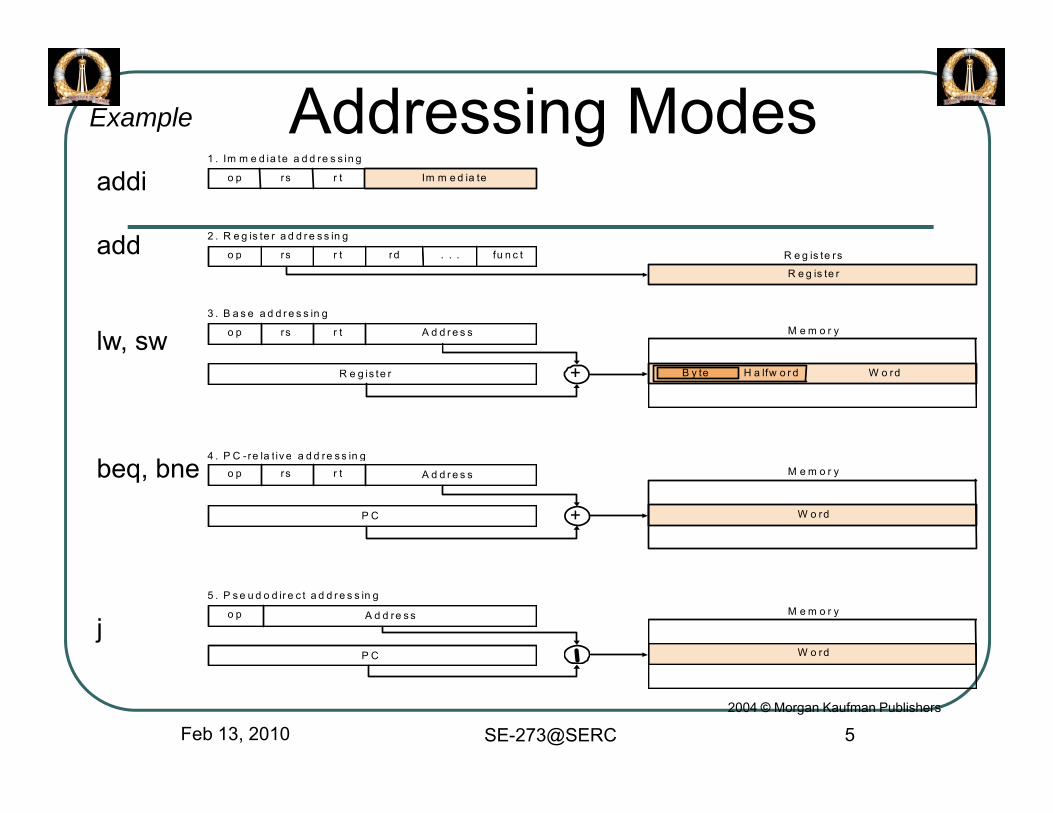
Addressing ModesExample
R i t
1 . Im m e d ia te a d d re s s in g
2 . R e g is te r a d d r e s s in g
o p rs r t
o p rs r t rd fu n c t
Im m e d ia teaddi
add R e g is te rs
M e m o r y
R e g is te r
3 . B a s e a d d r e s s in g
o p rs r t
o p rs r t A d d r e s s
rd . . . fu n c tadd
lw, swB y te H a lfw o r d W o rdR e g is te r
4 P C -re la tiv e a d d re s s in g
+
M e m o r y
W o rd
4 . P C re la tiv e a d d re s s in go p rs r t A d d r e s s
P C +
beq, bne
M e m o r y
W o rd
5 . P s e u d o d ir e c t a d d r e s s in g
o p A d d re s s
P C
j
Feb 13, 2010 SE-273@SERC 52004 © Morgan Kaufman Publishers
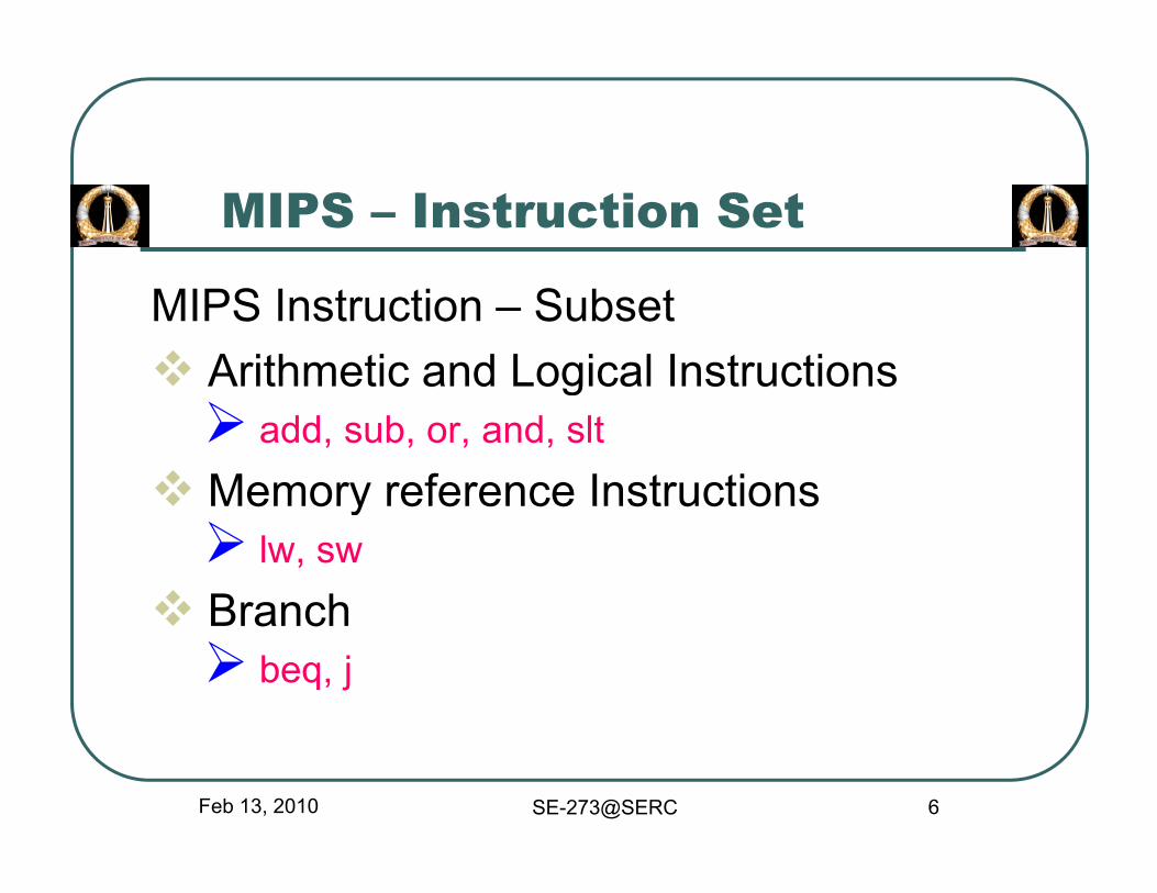
MIPS – Instruction Set
MIPS Instruction – SubsetArithmetic and Logical Instructionsg
add, sub, or, and, slt
Memory reference InstructionsMemory reference Instructionslw, sw
BranchBranchbeq, j
Feb 13, 2010 SE-273@SERC 6
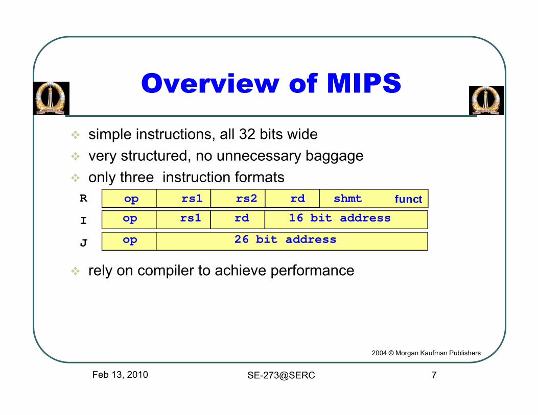
O i f MIPSi l i t ti ll 32 bit id
Overview of MIPSsimple instructions, all 32 bits widevery structured, no unnecessary baggageonly three instruction formatsonly three instruction formats
functop rs1 rs2 rd shmt
op rs1 rd 16 bit address
R
I
rely on compiler to achieve performance
op 26 bit addressJ
Feb 13, 2010 SE-273@SERC 7
2004 © Morgan Kaufman Publishers
Where Does It All Begin?
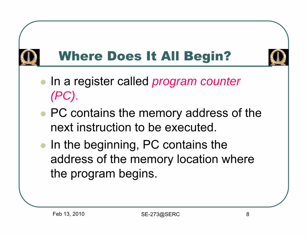
In a register called program counter (PC).PC contains the memory address of the next instruction to be executed.In the beginning, PC contains the address of the memory location where ythe program begins.
Feb 13, 2010 SE-273@SERC 8
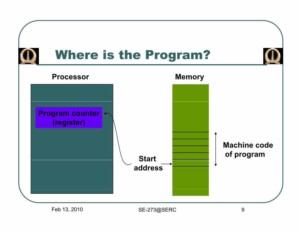
Where is the Program?MemoryProcessor
Program counter(register)
Machine codeof programStartStart
address
Feb 13, 2010 SE-273@SERC 9
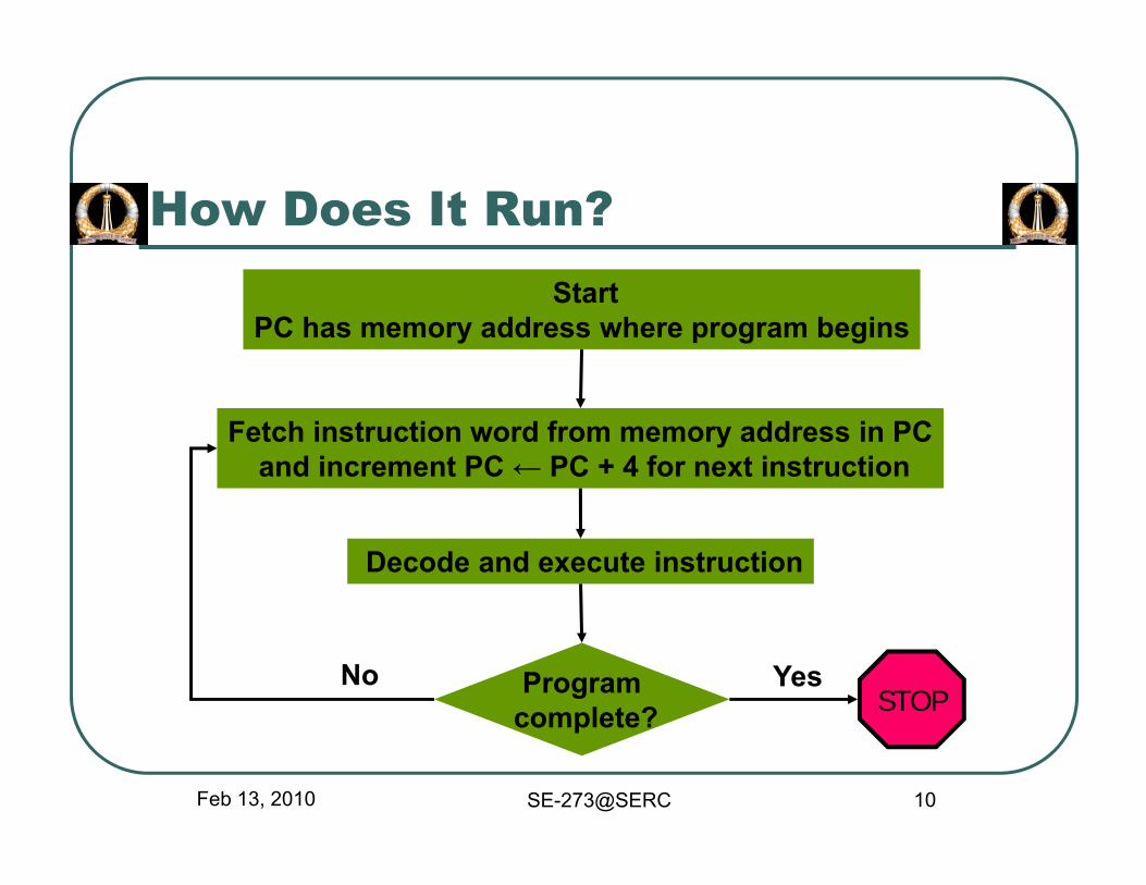
How Does It Run?Start
PC has memory address where program begins
Fetch instruction word from memory address in PCand increment PC ← PC + 4 for next instruction
Decode and execute instruction
Programcomplete?
YesNoSTOP
Feb 13, 2010 SE-273@SERC 10
complete?

Datapath and Control
Datapath: Memory, registers, adders, ALU, and communication
buses. Each step (fetch, decode, execute) requires
communication (data transfer) paths between memory, registers
and ALU.
Control: Datapath for each step is set up by control signals that
set up dataflow directions on communication buses and select
ALU and memory functions. Control signals are generated by a
control unit consisting of one or more finite-state machines.
Feb 13, 2010 SE-273@SERC 11
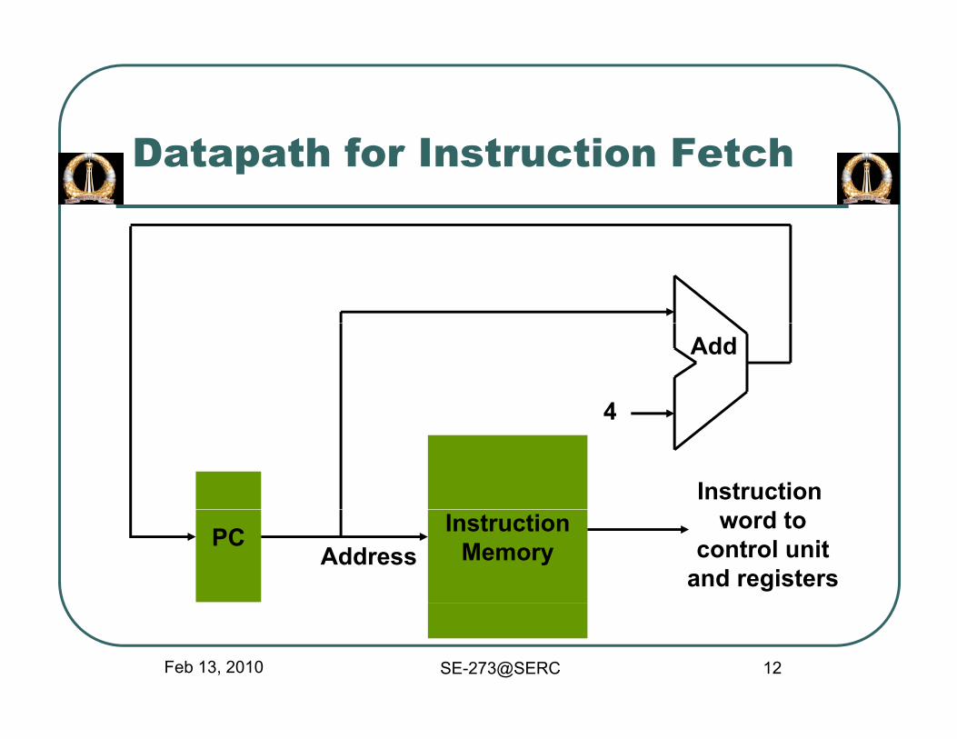
Datapath for Instruction Fetch
4
Add
4
Instruction
PC InstructionMemoryAddress
word tocontrol unit
and registers
Feb 13, 2010 SE-273@SERC 12

Register File: A Datapath ComponentRegister File: A Datapath Component
reg 1 data
5
5
32reg 1Read
registers32 Registers
(reg. file)Write
5
5
reg 2registers
Writeregister
reg 2 data
5
32
32
Write data32
RegWritefrom control
Feb 13, 2010 SE-273@SERC 13
from control
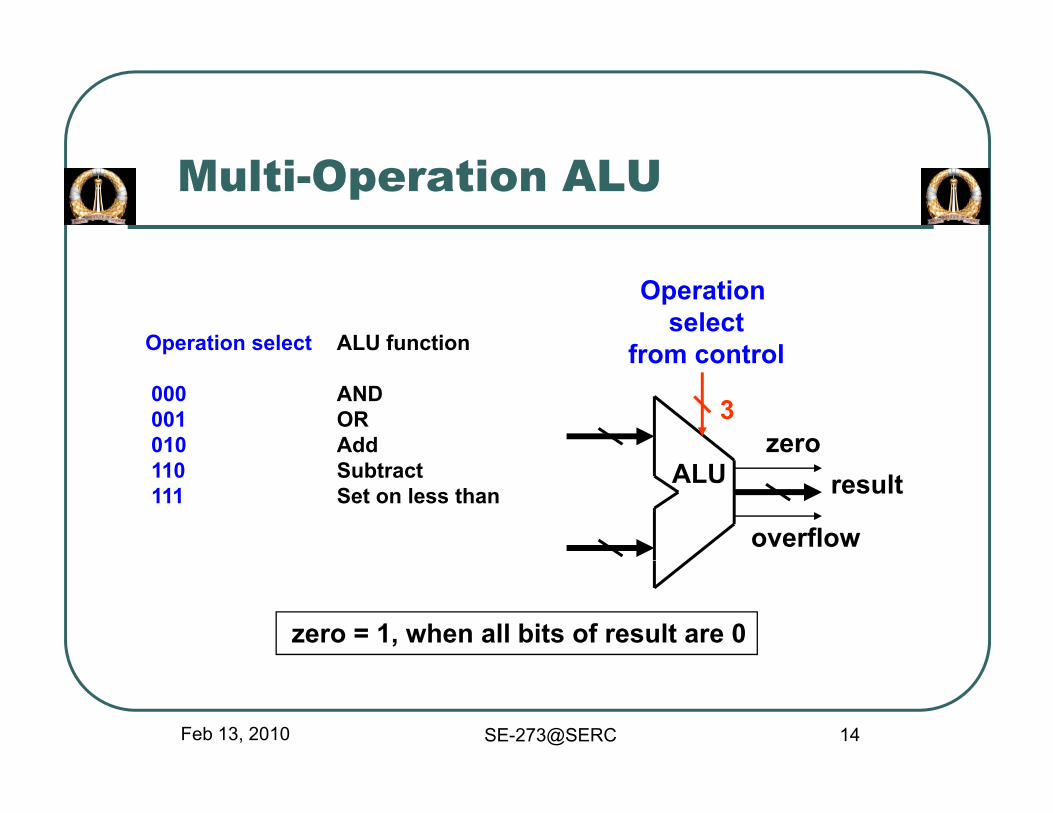
Multi-Operation ALU
Operationselect
from controlOperation select ALU function
3zero
from control000 AND001 OR010 Add
ALU result
overflow
110 Subtract111 Set on less than
zero = 1, when all bits of result are 0
Feb 13, 2010 SE-273@SERC 14

R T I t tiR-Type Instructions
Also known as arithmetic logical instructionsAlso known as arithmetic-logical instructionsadd, sub, sltE l dd $t0 $ 1 $ 2Example: add $t0, $s1, $s2• Machine instruction word
000000 10001 10010 01000 00000 100000000000 10001 10010 01000 00000 100000opcode $s1 $s2 $t0 function
• Read two registersRead two registers• Write one register• Opcode and function code go to control unit that
Feb 13, 2010 SE-273@SERC 15
generates RegWrite and ALU operation code.

Datapath for R-Type Instructionp yp
Operation000000 10001 10010 01000 00000 100000 000000 10001 10010 01000 00000 100000
5
32$s1Read
register 3
selectfrom control (add)
1000
1
opcode $s1 $s2 $t0opcode $s1 $s2 $t0 function (add)function (add)
32 Registers( fil )Write reg.
532
$s2
registernumbers
ALU
3zero
result
110
010
(reg. file)Write reg.number 5 overflow
0100
0 32$t0
32Write data
RegWrite from control
Feb 13, 2010 SE-273@SERC 16
activated

Load and Store Instructions
I-type instructionslw $t0, 1200 ($t1) # incr. in bytes
100011 01001 01000 0000 0100 1011 0000opcode $t1 $t0 1200
sw $t0, 1200 ($t1) # incr. in bytes, ( ) y101011 01001 01000 0000 0100 1011 0000opcode $t1 $t0 1200
Feb 13, 2010 SE-273@SERC 17
opcode $t1 $t0 1200
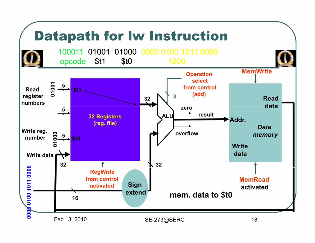
Datapath for lw Instruction
Operation MemWrite
100011 100011 01001 01000 01001 01000 0000 0100 1011 00000000 0100 1011 0000opcodeopcode $t1 $t0$t1 $t0 12001200
Operationselect
from control(add)
5
32$t1Read
registernumbers
30100
1
Readdata
32 Registers(reg. file)
Write reg.number
5
5
ALUzero
result
overflow00
Datamemory
Addr.
data
$t0number 5
32Write data
0100
320
e o y$t0Writedata
RegWritefrom control
activated Signextend
1600 1
011
0000
MemReadactivated
mem. data to $t0
Feb 13, 2010 SE-273@SERC 18
16
0000
010
$
Datapath for sw Instruction
MemWrite activated
101011 101011 01001 01000 01001 01000 0000 0100 1011 00000000 0100 1011 0000opcodeopcode $t1 $t0$t1 $t0 12001200
Operationselect
from control(add)
5
32$t1Read
register 30100
1
Read
MemWrite activated
32 Registers(reg. file)
5 $t0
gnumbers
ALUzero
result
flData
Addr.
data
0100
0
Write reg.number
5
32Write data
overflow
32
memory
$t0 data to mem.Writedata
32
32
RegWritefrom control
32
Signextend0
1011
000
0
MemRead
Feb 13, 2010 SE-273@SERC 19
e te d16
0000
010

Branch Instruction (I-Type)
beq $s1, $s2, 25 # if $s1 = $s2, advance PC through
25 instructions16-bits
000100 10001 10010 0000 0000 0001 1001opcode $s1 $s2 25opcode $s1 $s2 25
Note: Can branch within ± 215 words from the current instructionaddress in PC.
Feb 13, 2010 SE-273@SERC 20
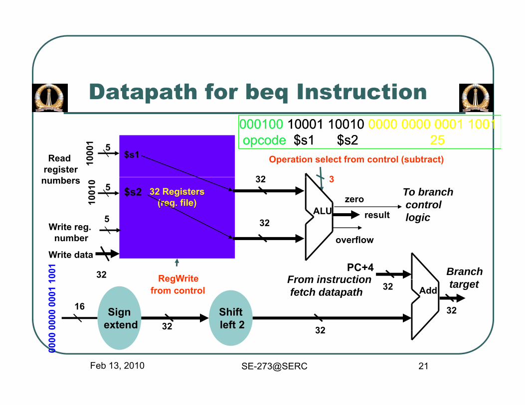
Datapath for beq Instruction000100000100 10001 1001010001 10010 0000 0000 0001 10010000 0000 0001 1001
Operation select from control (subtract)5
32
$s1Readregister
b 3
1000
1
000100000100 10001 10010 10001 10010 0000 0000 0001 10010000 0000 0001 1001opcode opcode $s1 $s2$s1 $s2 2525
32 Registers(reg. file)
Write reg
5
5
32numbers
ALU
3
zeroresult
1001
0
$s2
32
To branchcontrollogic
Write reg.number
32
Write dataoverflow
RegWrite001 PC+4
From instructionBranch
RegWritefrom control
32Sign
extend
16
0000
000
1 1
Shiftleft 2
Add
32
32From instructionfetch datapath
target
32
Feb 13, 2010 SE-273@SERC 21
0000
32
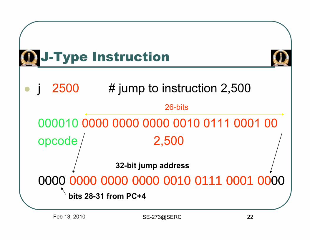
J-Type Instruction
j 2500 # jump to instruction 2,50026 bit26-bits
000010 0000 0000 0000 0010 0111 0001 00opcode 2,500
32 bit jump address
0000 0000 0000 0000 0000 0010 0111 0001 000000 0000 0000 0010 0111 0001 000000bits 28 31 from PC+4
32-bit jump address
Feb 13, 2010 SE-273@SERC 22
bits 28-31 from PC+4
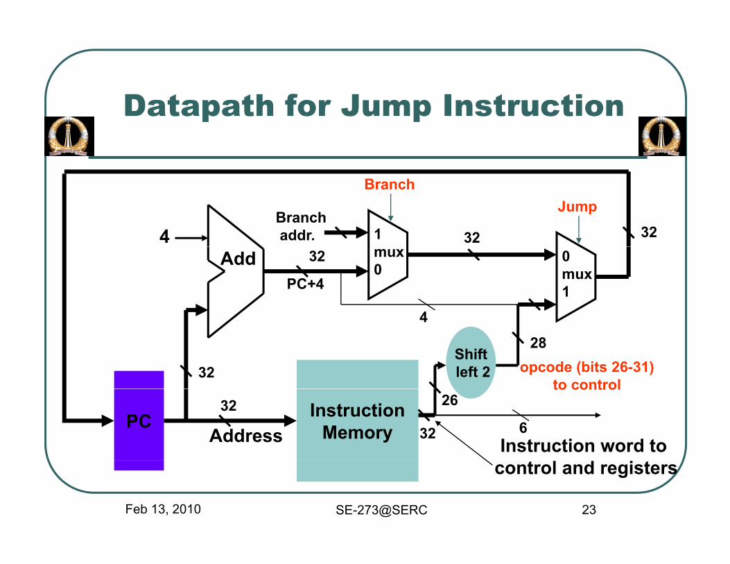
Datapath for Jump InstructionDatapath for Jump Instruction
4 1Branchaddr.
BranchJump
32 32
Add mux0
0mux1
32
4
PC+4
opcode (bits 26-31)to control
Shiftleft 2
28
4
32
PC InstructionMemoryAddress Instruction word to
to control
6
2632
32
Feb 13, 2010 SE-273@SERC 23
control and registers
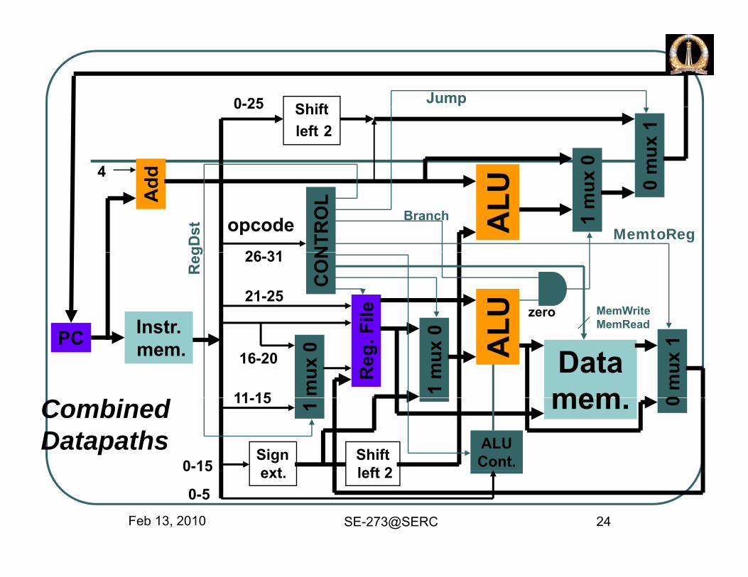
Shift0-25 Jump
dd x 0
4 U mux
1
Shiftleft 2
0 25
Ad
1 m
ux
NTR
OL
opcode Branch
26 31
ALU
0
gDst MemtoReg
Instr File
CO
NMemWriteMemReadLU zero
21-25
26-31
Reg
Instr.mem.PC
Reg
. FDatamem1
mux
0
0 m
ux 1
mux
0MemRead
AL
11 15
16-20
mem. 01
Signext
Shiftleft 2
ALUCont.0-15
11-15CombinedDatapaths
Feb 13, 2010 SE-273@SERC 24
ext. left 20 15
0-5

ControlRegDstg
Jump
Branch
ControlLogic
Instruction
bits 26 31
MemRead
MemtoReg
ALUOpbits 26-31opcode
ALUOp
MemWrite
ALUSrc
RegWrite
ALUInstruction2
Feb 13, 2010 SE-273@SERC 25
ALUControlbits 0-5
funct.
to ALU
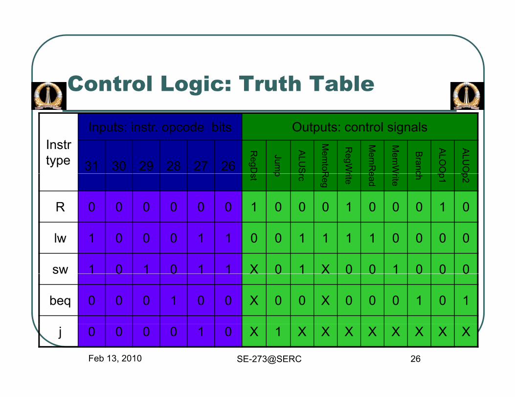
Control Logic: Truth Table
I t i t d bit O t t t l i lInstr type
Inputs: instr. opcode bits Outputs: control signals
31 30 29 28 27 26
RegD
Jump
ALUS
Mem
to R
RegW
r
Mem
Re
Mem
W
Branc
ALOO
ALUO
pst
p rc Reg
rite
ead
Write
ch p1 p2
R 0 0 0 0 0 0 1 0 0 0 1 0 0 0 1 0
lw 1 0 0 0 1 1 0 0 1 1 1 1 0 0 0 0
sw 1 0 1 0 1 1 X 0 1 X 0 0 1 0 0 0s 0 0 0 0 0 0 0 0
beq 0 0 0 1 0 0 X 0 0 X 0 0 0 1 0 1
Feb 13, 2010 SE-273@SERC 26
j 0 0 0 0 1 0 X 1 X X X X X X X X

How Long Does It Take?Assume control logic is fast and does notAssume control logic is fast and does not affect the critical timing. Major time delay components are ALU memory read/writecomponents are ALU, memory read/write, and register read/write.Arithmetic type (R type)Arithmetic-type (R-type)
•Fetch (memory read) 2ns•Register read 1nsRegister read 1ns•ALU operation 2ns•Register write 1ns
Feb 13, 2010 SE-273@SERC 27
•Total 6ns
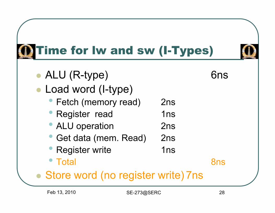
Time for lw and sw (I-Types)
ALU (R-type) 6nsLoad word (I-type)( yp )• Fetch (memory read) 2ns• Register read 1ns• ALU operation 2ns• Get data (mem. Read) 2ns• R i t it 1• Register write 1ns• Total 8ns
Store word (no register write) 7nsFeb 13, 2010 SE-273@SERC 28
Store word (no register write) 7ns
Time for beq (I-Type)
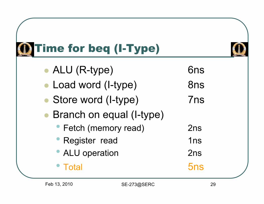
ALU (R-type) 6nsLoad word (I-type) 8ns( yp )Store word (I-type) 7nsBranch on equal (I-type)Branch on equal (I-type)• Fetch (memory read) 2ns• Register read 1nsRegister read 1ns• ALU operation 2ns• Total 5ns
Feb 13, 2010 SE-273@SERC 29
• Total 5ns
Time for Jump (J-Type)
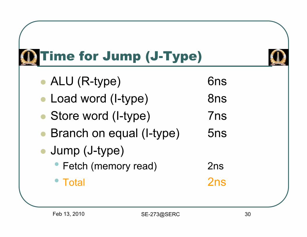
ALU (R-type) 6nsLoad word (I-type) 8ns( yp )Store word (I-type) 7nsBranch on equal (I-type) 5nsBranch on equal (I-type) 5nsJump (J-type)• F t h ( d) 2• Fetch (memory read) 2ns• Total 2ns
Feb 13, 2010 SE-273@SERC 30

How Fast Can the Clock Be?
If every instruction is executed in one clock cycle, then:• Clock period must be at least 8ns to perform the
longest instruction, i.e., lw.• This is a single cycle machine.• It is slower because many instructions take less
th 8 b t till ll d th t h tithan 8ns but are still allowed that much time.
Method of speeding up: Use multicycle d t th
Feb 13, 2010 SE-273@SERC 31
datapath.
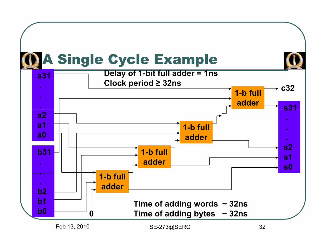
A Single Cycle Examplea31 Delay of 1-bit full adder = 1nsa31...
1-b fulladder s31
c32Clock period ≥ 32ns
a2a1a0
1-b fulladder
s31...
b31.
1-b fulladder
s2s1s0.
.b2b1
1-b fulladder
Time of adding words ~ 32ns
Feb 13, 2010 SE-273@SERC 32
b0 0Time of adding words 32nsTime of adding bytes ~ 32ns
A Multicycle Implementationa31 Delay of 1-bit full adder = 1nsa31...hi
ft
Delay of 1-bit full adder = 1nsClock period ≥ 1ns
Time of adding words ~ 32ns.a2a1a0 1 b full
Sh
Time of adding words 32nsTime of adding bytes ~ 8ns
b31.
1-b fulladder s31
.c32 t.
.b2b1
.
.s2s1
c32 FF
Initializeto 0
Shift
Shift
Feb 13, 2010 SE-273@SERC 33
b1b0
s1s0
to 0

Multicycle Datapath
(IR)
.
PC
str.
reg.
DR
)
ut R
eg.
A R
eg.
LU
ster
file
mor
y
Addr.In
s
Dat
a (M
D
ALU
Ou
B R
eg. AL
Reg
is
Mem
Data 4M
em. B
Feb 13, 2010 SE-273@SERC 34
One-cycle data transfer paths(need registers to hold data)

Multicycle Datapath Requirements
Only one ALU, since it can be reused.Single memory for instructions and data.g yFive registers added:• Instruction register (IR)Instruction register (IR)• Memory data register (MDR)• Three ALU registers, A and B for inputs andThree ALU registers, A and B for inputs and
ALUOut for output
Feb 13, 2010 SE-273@SERC 35
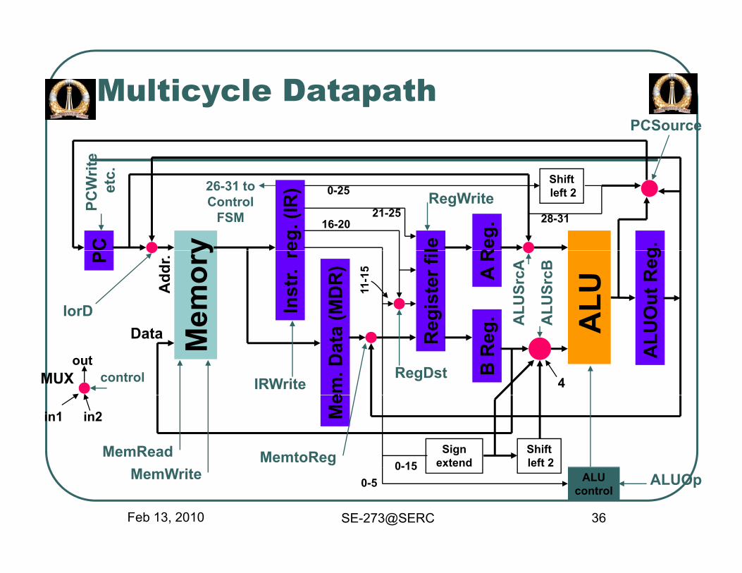
Multicycle Datapathy p
Shift
PCSource
Writ
ec.
C eg. (
IR)
g.Reg
. ley16-20
21-25RegWrite
Shiftleft 20-25
28-31
PCW et
c
26-31 toControl
FSM
P
Inst
r. re
(MD
R)
UO
ut R
egA R
g. ALU
egis
ter f
il
emor
yA
ddr.
IorD ALU
SrcB
ALU
SrcA
11-1
5
em. D
ata
ALU
B R
eg ARe
Me
Data
4
AA
RegDstIRWrite
outcontrolMUX
Me
Signextend
Shiftleft 20-15MemtoRegMemRead
in1 in2
Feb 13, 2010 SE-273@SERC 36
ALUcontrol
0-50-15
ALUOpMemWrite
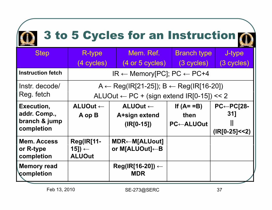
3 to 5 Cycles for an Instruction3 to 5 Cycles for an InstructionStep R-type
(4 cycles)Mem. Ref.
(4 or 5 cycles)Branch type(3 cycles)
J-type(3 cycles)( y ) ( y ) ( y ) ( y )
Instruction fetch IR ← Memory[PC]; PC ← PC+4
Instr. decode/ R f t h
A ← Reg(IR[21-25]); B ← Reg(IR[16-20])Reg. fetch ALUOut ← PC + (sign extend IR[0-15]) << 2Execution, addr. Comp.,
ALUOut ←A op B
ALUOut ←A+sign extend
If (A= =B)then
PC←PC[28-31]
branch & jump completion
p g(IR[0-15]) PC←ALUOut ||
(IR[0-25]<<2)Mem. Access Reg(IR[11- MDR←M[ALUout] or R-type completion
15]) ← ALUOut
or M[ALUOut]←B
Memory read l ti
Reg(IR[16-20]) ← MDR
Feb 13, 2010 SE-273@SERC 37
completion MDR
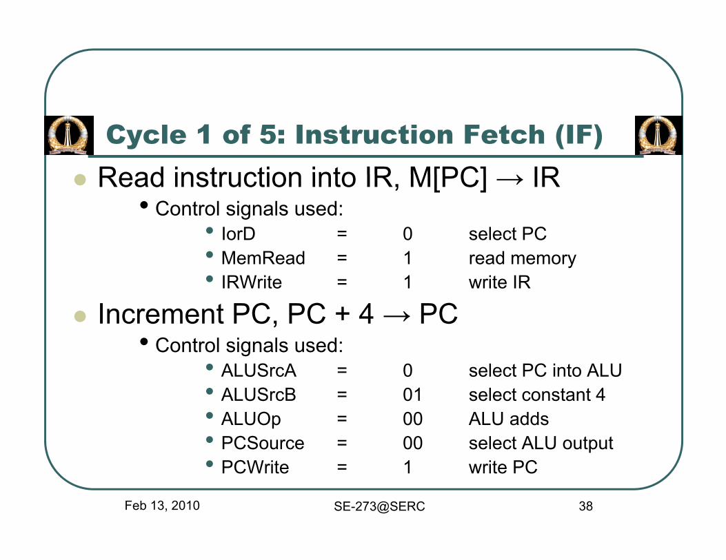
Cycle 1 of 5: Instruction Fetch (IF)Read instruction into IR M[PC] IRRead instruction into IR, M[PC] → IR
• Control signals used:• IorD = 0 select PC• MemRead = 1 read memory• IRWrite = 1 write IR
Increment PC PC + 4 → PCIncrement PC, PC + 4 → PC• Control signals used:
• ALUSrcA = 0 select PC into ALU• ALUSrcB = 01 select constant 4• ALUOp = 00 ALU adds• PCSource = 00 select ALU output
Feb 13, 2010 SE-273@SERC 38
• PCWrite = 1 write PC
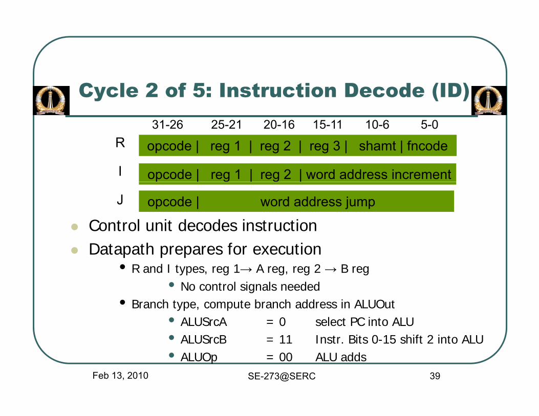
Cycle 2 of 5: Instruction Decode (ID)31-26 25-21 20-16 15-11 10-6 5-0
opcode | reg 1 | reg 2 | reg 3 | shamt | fncode
opcode | reg 1 | reg 2 | word address increment
R
I
Control unit decodes instructionopcode | word address jumpJ
Datapath prepares for execution• R and I types, reg 1→ A reg, reg 2 → B reg
• No control signals needed• No control signals needed• Branch type, compute branch address in ALUOut
• ALUSrcA = 0 select PC into ALU• ALUSrcB = 11 Instr Bits 0-15 shift 2 into ALU
Feb 13, 2010 SE-273@SERC 39
• ALUSrcB = 11 Instr. Bits 0-15 shift 2 into ALU• ALUOp = 00 ALU adds

Cycle 3 of 5: Execute (EX)R type: execute function on reg A and reg B result inR type: execute function on reg A and reg B, result in ALUOut
• Control signals used:• ALUSrcA = 1 A reg into ALU• ALUsrcB = 00 B reg into ALU• ALUOp = 10 instr. Bits 0-5 control ALU
I type, lw or sw: compute memory address in ALUOut ← A reg + sign extend IR[0-15]
• Control signals used:Control signals used:• ALUSrcA = 1 A reg into ALU• ALUSrcB = 10 Instr. Bits 0-15 into ALU• ALUOp = 00 ALU adds
Feb 13, 2010 SE-273@SERC 40
p
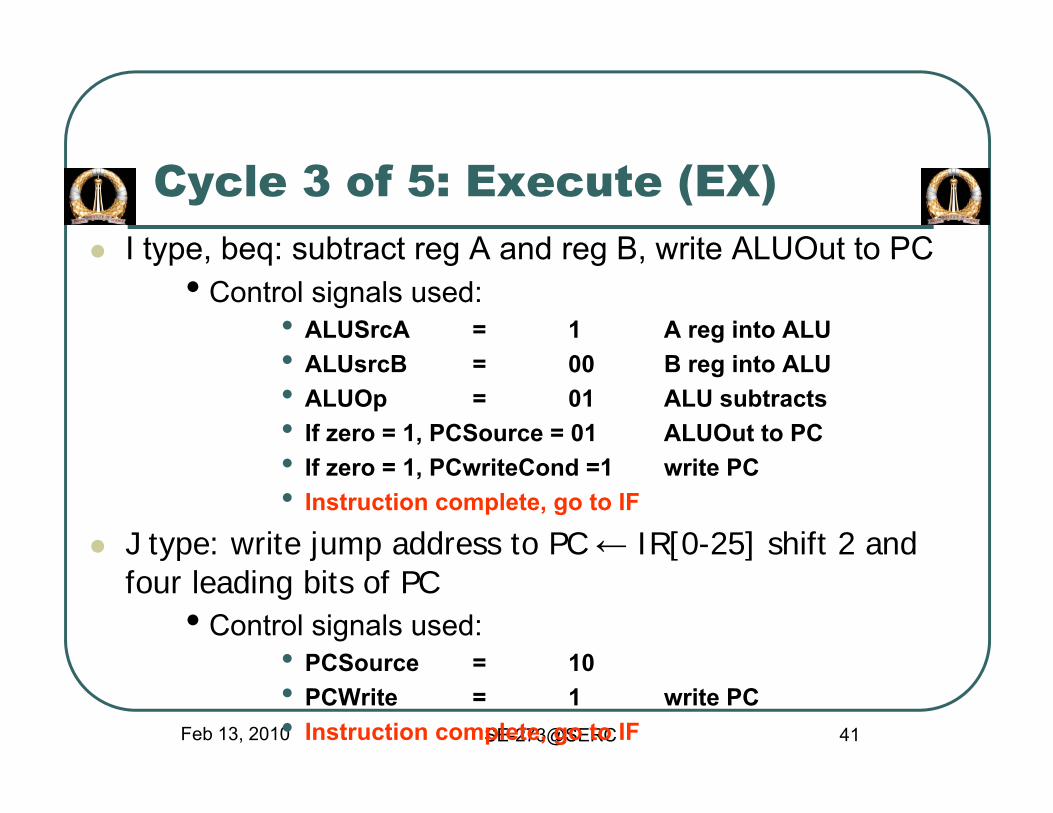
Cycle 3 of 5: Execute (EX)I type beq: subtract reg A and reg B write ALUOut to PCI type, beq: subtract reg A and reg B, write ALUOut to PC
• Control signals used:• ALUSrcA = 1 A reg into ALU• ALU B 00 B i t ALU• ALUsrcB = 00 B reg into ALU• ALUOp = 01 ALU subtracts• If zero = 1, PCSource = 01 ALUOut to PC• If zero = 1, PCwriteCond =1 write PC• Instruction complete, go to IF
J type: write jump address to PC ← IR[0-25] shift 2 and yp j pfour leading bits of PC
• Control signals used:• PCSource = 10
Feb 13, 2010 SE-273@SERC 41
PCSource = 10• PCWrite = 1 write PC• Instruction complete, go to IF
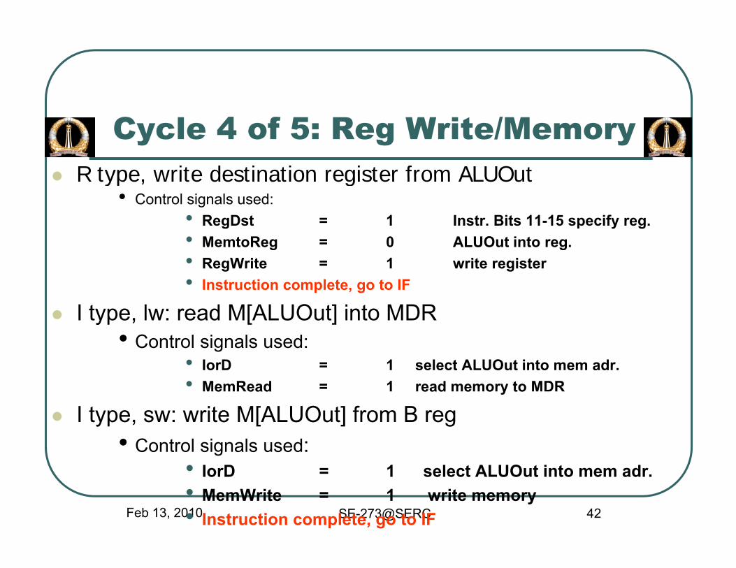
Cycle 4 of 5: Reg Write/MemoryR type write destination register from ALUOutR type, write destination register from ALUOut
• Control signals used:• RegDst = 1 Instr. Bits 11-15 specify reg.• MemtoReg = 0 ALUOut into reg.g g• RegWrite = 1 write register• Instruction complete, go to IF
I type, lw: read M[ALUOut] into MDRI type, lw: read M[ALUOut] into MDR• Control signals used:
• IorD = 1 select ALUOut into mem adr.• MemRead = 1 read memory to MDRe ead ead e o y to
I type, sw: write M[ALUOut] from B reg• Control signals used:
Feb 13, 2010 SE-273@SERC 42
• IorD = 1 select ALUOut into mem adr.• MemWrite = 1 write memory• Instruction complete, go to IF
Cycle 5 of 5: Reg Write
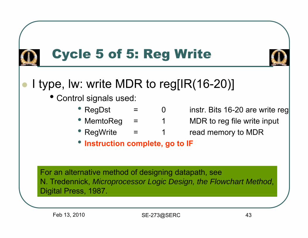
I type, lw: write MDR to reg[IR(16-20)]• Control signals used:
• RegDst = 0 instr. Bits 16-20 are write reg• MemtoReg = 1 MDR to reg file write input• RegWrite = 1 read memory to MDRRegWrite 1 read memory to MDR• Instruction complete, go to IF
For an alternative method of designing datapath, seeN. Tredennick, Microprocessor Logic Design, the Flowchart Method,Digital Press, 1987.
Feb 13, 2010 SE-273@SERC 43
g ,
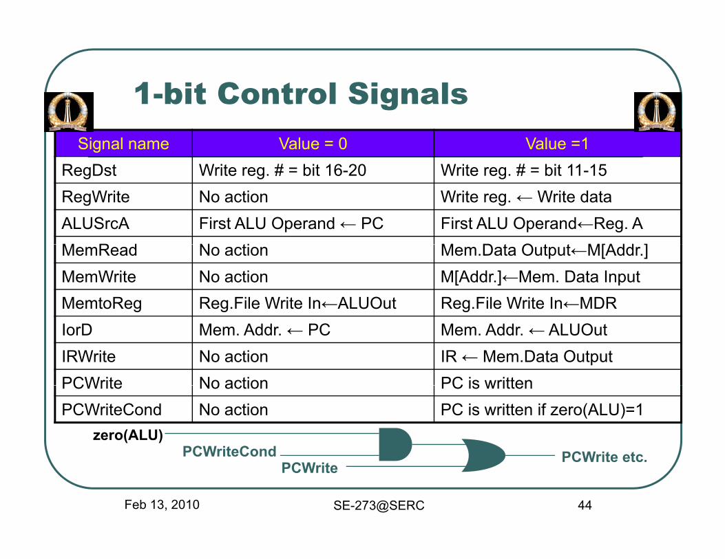
1-bit Control Signals1 bit Control SignalsSignal name Value = 0 Value =1
RegDst Write reg # = bit 16-20 Write reg # = bit 11-15RegDst Write reg. # bit 16 20 Write reg. # bit 11 15RegWrite No action Write reg. ← Write dataALUSrcA First ALU Operand ← PC First ALU Operand←Reg. AM R d N ti M D t O t t M[Add ]MemRead No action Mem.Data Output←M[Addr.]MemWrite No action M[Addr.]←Mem. Data InputMemtoReg Reg.File Write In←ALUOut Reg.File Write In←MDRIorD Mem. Addr. ← PC Mem. Addr. ← ALUOutIRWrite No action IR ← Mem.Data OutputPCWrite No action PC is writtenPCWrite No action PC is writtenPCWriteCond No action PC is written if zero(ALU)=1
PCWrite etcPCWriteCondzero(ALU)
Feb 13, 2010 SE-273@SERC 44
PCWrite etc.PCWrite
PCWriteCond

2 bit C t l Si l2-bit Control Signals
Signal name Value ActionSignal name Value Action
ALUOp00 ALU performs add01 ALU performs subtract10 Funct. field (0-5 bits of IR ) determines ALU operation
ALUSrcB00 Second input of ALU ← B reg.01 Second input of ALU ← 4 (constant)( )10 Second input of ALU ← 0-15 bits of IR sign ext. to 32b11 Second input of ALU ← 0-15 bits of IR sign ext. and left shift
2 bits
PCSource00 ALU output (PC +4) sent to PC01 ALUOut (branch target addr.) sent to PC10 Jump address IR[0 25] shifted left 2 bits concatenated with
Feb 13, 2010 SE-273@SERC 45
10 Jump address IR[0-25] shifted left 2 bits, concatenated with PC+4[28-31], sent to PC

Control: Finite State Machine
Start
Instruction fetchState 0Clock
cycle 1
Instruction decode and register fetch
Instruction fetchState 1
cycle 1
Clockcycle 2
MemoryFSM-M
FSM-R FSM-B FSM-JClock yaccessinstr.
R-typeinstr.
Branchinstr.
Jumpinstr.
Clockcycles 3-5
Feb 13, 2010 SE-273@SERC 46

State 0: Instruction Fetch (CC1)State 0: Instruction Fetch (CC1)
Shift
PCSource=00
Writ
e.=
1C eg
. (IR
)
g.Reg
. ley16-20
21-25RegWrite
Shiftleft 20-25
28-31
PCW
etc. 26-31 to
ControlFSM
P
Inst
r. re
(MD
R)
UO
ut R
egA R
g. ALU
egis
ter f
il
emor
yA
ddr.
IorD=0
LUSr
cB=0
1
LUSr
cA=0
em. D
ata
ALU
B R
eg ARe
Me
Data
4
ALAL
RegDstIRWrite
outcontrolMUX Add
Me
Signextend
Shiftleft 20-15MemtoReg
=1
MemRead = 1
in1 in2
Feb 13, 2010 SE-273@SERC 47
ALUcontrol
0-50-15MemtoReg
ALUOp=00
MemWrite
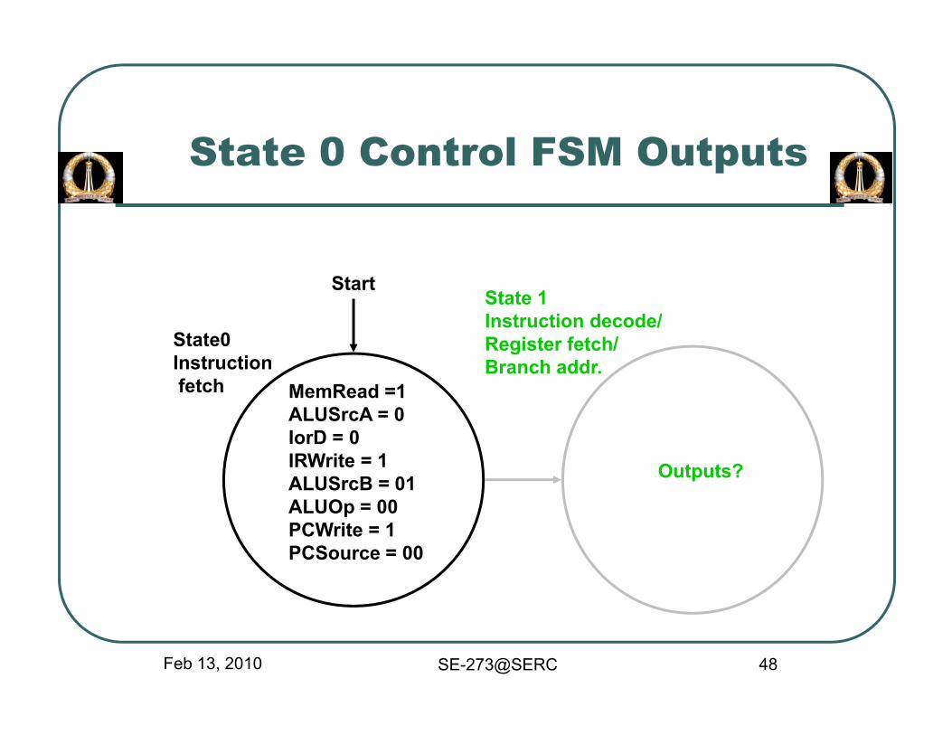
State 0 Control FSM Outputs
Start State 1Instruction decode/
MemRead =1ALUSrcA = 0
State0Instructionfetch
Instruction decode/Register fetch/Branch addr.
ALUSrcA = 0IorD = 0IRWrite = 1ALUSrcB = 01ALUOp = 00
Outputs?
ALUOp = 00PCWrite = 1PCSource = 00
Feb 13, 2010 SE-273@SERC 48
State 1: Instr. Decode/Reg. Fetch/ Branch Address (CC2)Branch Address (CC2)
Shift
PCSource
Writ
ec.
C eg. (
IR)
g.Reg
. ley16-20
21-25
0
RegWriteShiftleft 20-25
28-31
PCW et
c
26-31 toControl
FSM
P
Inst
r. re
(MD
R)
UO
ut R
egA R
g. ALU
egis
ter f
il
emor
yA
ddr.
IorD
LUSr
cB=1
1
ALU
SrcA
=0
em. D
ata
ALU
B R
eg ARe
Me
Data
4
ALA
RegDstIRWrite
outcontrolMUX Add
Me
Signextend
Shiftleft 20-15MemtoRegMemRead
in1 in2
Feb 13, 2010 SE-273@SERC 49
ALUcontrol
0-50-15 ALUOp
= 00MemWrite

State 1 Control FSM OutputsStart
State 1I t ti d d (ID) /
MemRead =1ALUSrcA = 0
Start State0Instructionfetch(IF)
Instruction decode (ID) /Register fetch /Branch addr.
ALUSrcA = 0IorD = 0IRWrite = 1ALUSrcB = 01ALUOp = 00
(IF)
ALUSrcA = 0ALUSrcB = 11ALUOp = 00ALUOp = 00
PCWrite = 1PCSource = 00
FSM-M FSM-R FSM-B FSM-J
Opcode = J-typeOpcode= BEQ
Feb 13, 2010 SE-273@SERC 50

State 1 (Opcode = lw) → FSM-M (CC3-5)
Shift
PCSource
Writ
ec.
CC4
C eg. (
IR)
g.Reg
. le
16-2021-25
0
RegWrite=1Shiftleft 20-25
28-31
PCW et
c
26-31 toControl
FSMy CC3P
Inst
r. re
(MD
R)
UO
ut R
egA R
g. ALU
egis
ter f
il
Add
r.
IorD=1
LUSr
cB=1
0
ALU
SrcA
=1
emor
y CC3
em. D
ata
ALU
B R
eg AReData
4
ALA
RegDst=0IRWrite
outcontrolMUX Add
Me
CC5
Me
Signextend
Shiftleft 20-15MemtoReg=1
RegDst=0
MemRead=1
in1 in2
Feb 13, 2010 SE-273@SERC 51
ALUcontrol
0-50-15 ALUOp
= 00MemWrite
State 1 (Opcode= sw)→FSM-M (CC3-4)
Shift
PCSource
Writ
ec.
CC4C eg
. (IR
)
g.Reg
. le
16-2021-25
0
RegWriteShiftleft 20-25
28-31
PCW et
c
26-31 toControl
FSMy CC3
P
Inst
r. re
(MD
R)
UO
ut R
egA R
g. ALU
egis
ter f
il
Add
r.
IorD=1
LUSr
cB=1
0
ALU
SrcA
=1
emor
y
em. D
ata
ALU
B R
eg AReData
4
ALA
RegDst=0IRWrite
outcontrolMUX Add
Me
Me
Signextend
Shiftleft 20-15MemtoRegMemRead
in1 in2 CC4
Feb 13, 2010 SE-273@SERC 52
ALUcontrol
0-50-15 ALUOp
= 00MemWrite=1
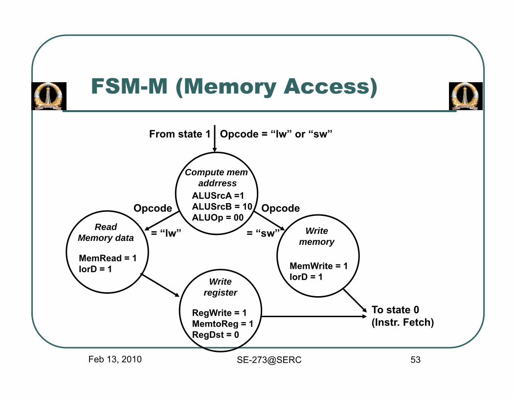
FSM-M (Memory Access)
Compute mem
From state 1 Opcode = “lw” or “sw”
ALUSrcA =1ALUSrcB = 10ALUOp = 00
Compute memaddrress
R d
Opcode Opcode
MemRead = 1IorD = 1 MemWrite = 1
I D 1
ReadMemory data
Writememory
= “lw” = “sw”
RegWrite = 1MemtoReg = 1
IorD = 1Writeregister
To state 0(Instr. Fetch)
Feb 13, 2010 SE-273@SERC 53
MemtoReg = 1RegDst = 0
(Instr. Fetch)
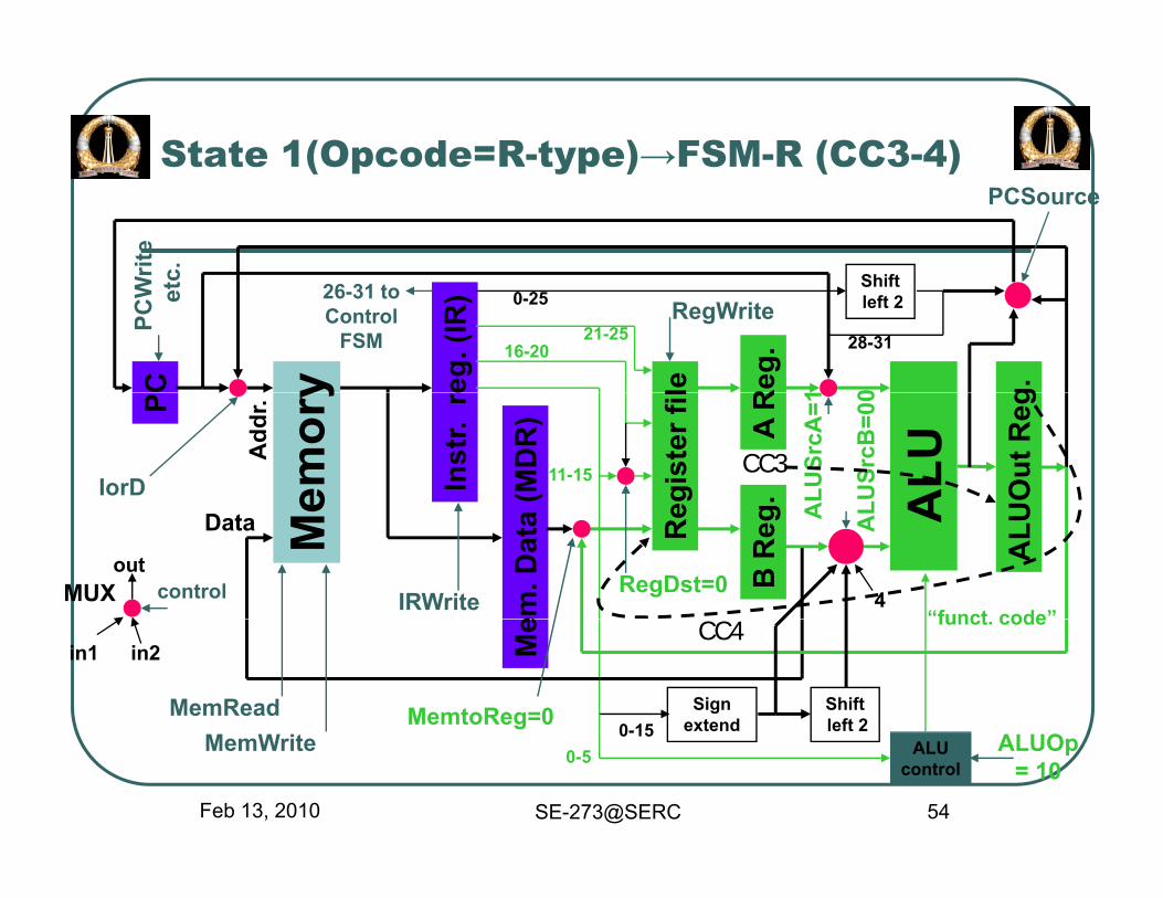
State 1(Opcode=R-type)→FSM-R (CC3-4)State 1(Opcode R type) FSM R (CC3 4)
Shift
PCSource
Writ
ec.
C eg. (
IR)
g.Reg
. le
16-2021-25
0
RegWriteShiftleft 20-25
28-31
PCW et
c
26-31 toControl
FSMyP
Inst
r. re
(MD
R)
UO
ut R
egA R
g. ALU
egis
ter f
il
Add
r.
IorD
LUSr
cB=0
0
ALU
SrcA
=1
emor
y
11-15 CC3
em. D
ata
ALU
B R
eg AReData
4
ALA
RegDst=0IRWrite
outcontrolMUX
Me
“funct code”
Me
Signextend
Shiftleft 20-15MemtoReg=0MemRead
in1 in2funct. codeCC4
Feb 13, 2010 SE-273@SERC 54
ALUcontrol
0-50-15 ALUOp
= 10MemWrite

FSM-R (R-type Instruction)FSM R (R type Instruction)
F t t 1 O d R t
ALUoperation
From state 1 Opcode = R-type
ALUSrcA =1ALUSrcB = 00ALUOp = 10
Write
RegWrite = 1MemtoReg = 0
Writeregister
To state 0(Instr. Fetch)
Feb 13, 2010 SE-273@SERC 55
gRegDst = 1

State 1 (Opcode = beq ) → FSM-B (CC3)If( )
Shift
PCSource01
Writ
e.=
1If(zero)
C eg. (
IR)
g.Reg
. le
16-20
21-25
0
RegWriteShiftleft 20-25
28-31
PCW
etc. 26-31 to
ControlFSM
yP
Inst
r. re
(MD
R)
UO
ut R
egA R
g. ALU
egis
ter f
il
Add
r.
IorD
LUSr
cB=0
0
ALU
SrcA
=1
emor
y
11-15 CC3
em. D
ata
ALU
B R
eg AReData
4
ALA
RegDstIRWrite
outcontrolMUX
Me
subtract
zero
Me
Signextend
Shiftleft 20-15MemtoRegMemRead
in1 in2
Feb 13, 2010 SE-273@SERC 56
ALUcontrol
0-50-15 ALUOp
= 01MemWrite
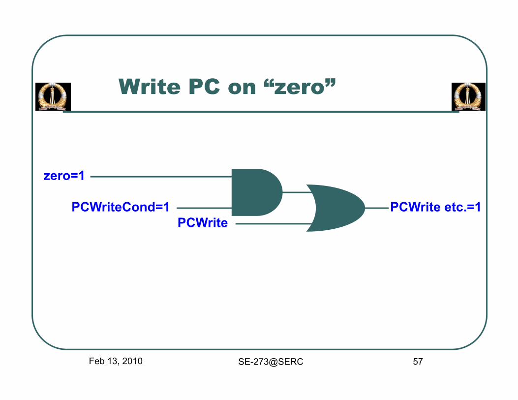
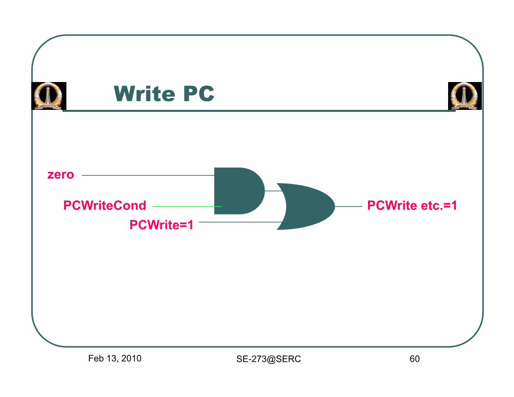
Write PC on “zero”
zero=1
PCWrite etc.=1PCWrite
PCWriteCond=1
zero=1
PCWrite
Feb 13, 2010 SE-273@SERC 57
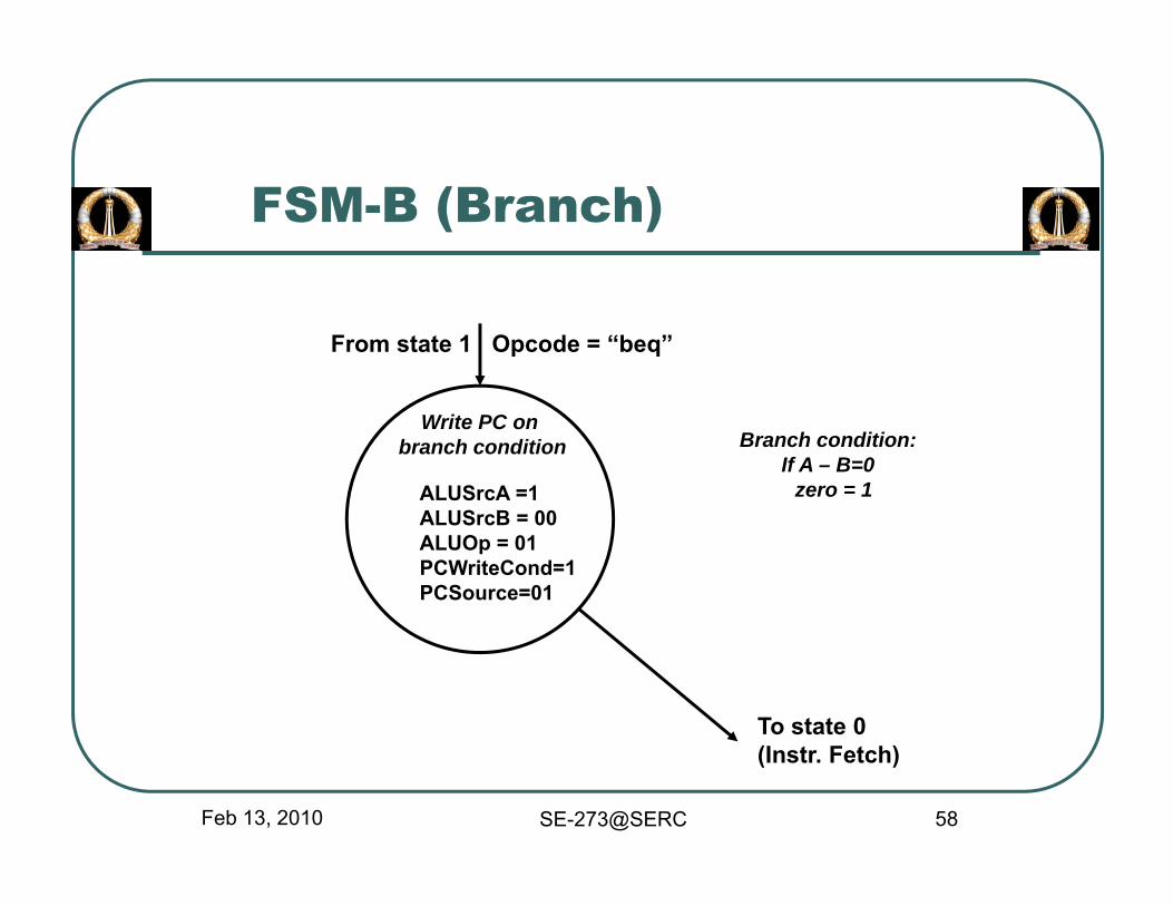
FSM-B (Branch)
From state 1 Opcode = “beq”
ALUSrcA =1ALUS B 00
Branch condition:If A – B=0
zero = 1
Write PC onbranch condition
ALUSrcB = 00ALUOp = 01PCWriteCond=1PCSource=01
To state 0
Feb 13, 2010 SE-273@SERC 58
(Instr. Fetch)
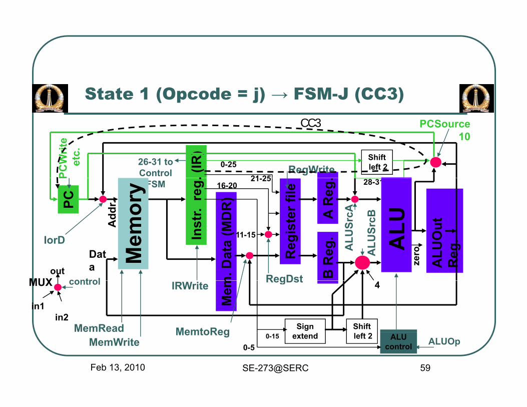
State 1 (Opcode = j) → FSM-J (CC3)PCSourceCC3
. (IR
)21 25
RegWriteShiftleft 20-25
PCSource10
PCW
rite
etc.
26-31 toControl
CC3
PC
nstr.
reg
.
MD
R)
ut A
Reg
.
ster
file
Add
r.
16-2021-25
SrcBSrcA
28-31
P
FSM
mor
y
LU
In
m. D
ata
(M
ALU
Ou
Reg
.
B R
eg.
Reg
is
Data
IorD
ALU
S
ALU
RegDstout
controlMUX
Mem 11-15
zeroA
L
Mem 4
Sign ShiftMemtoReg
RegDstIRWrite
MemRead
in1in2
controlMUX
Feb 13, 2010 SE-273@SERC 59
extend left 2 ALUcontrol0-5
0-15MemtoRegALUOpMemWrite
Write PC
zero
PCWrite etc.=1PCWrite=1
PCWriteCond
zero
PCWrite=1
Feb 13, 2010 SE-273@SERC 60

FSM-J (Jump)
From state 1 Opcode = “jump”
PCWrite=1PCSource=10
Writejump addr. In PC
PCSource=10
To state 0(Instr Fetch)
Feb 13, 2010 SE-273@SERC 61
(Instr. Fetch)

Control FSMStartState 0
Instr.decode/reg.fetch/branch
addr
Instr.fetch/
adv. PC
State 0 1
addr.
ALU Write PC WriteRead Computelw
RB
J23
ALUoperation
Write PCon branchcondition
jump addr.to PC
memorydata
pmemory
addr.
sw
6
8 9
Writememory
data
Writeregister
Writeregister
4 5 7
Feb 13, 2010 SE-273@SERC 62
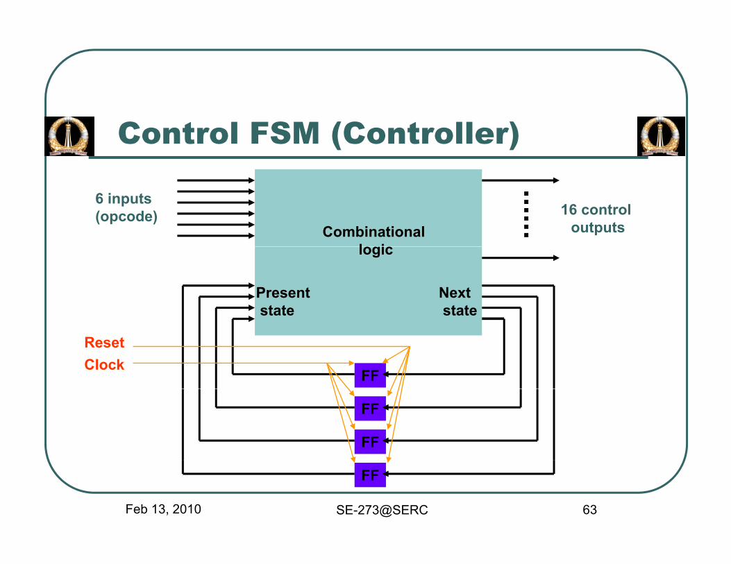
Control FSM (Controller)
Combinationall i
16 controloutputs
6 inputs(opcode)
logic
Nextstate
Presentstate
FFClockReset
FF
FF
Feb 13, 2010 SE-273@SERC 63
FF
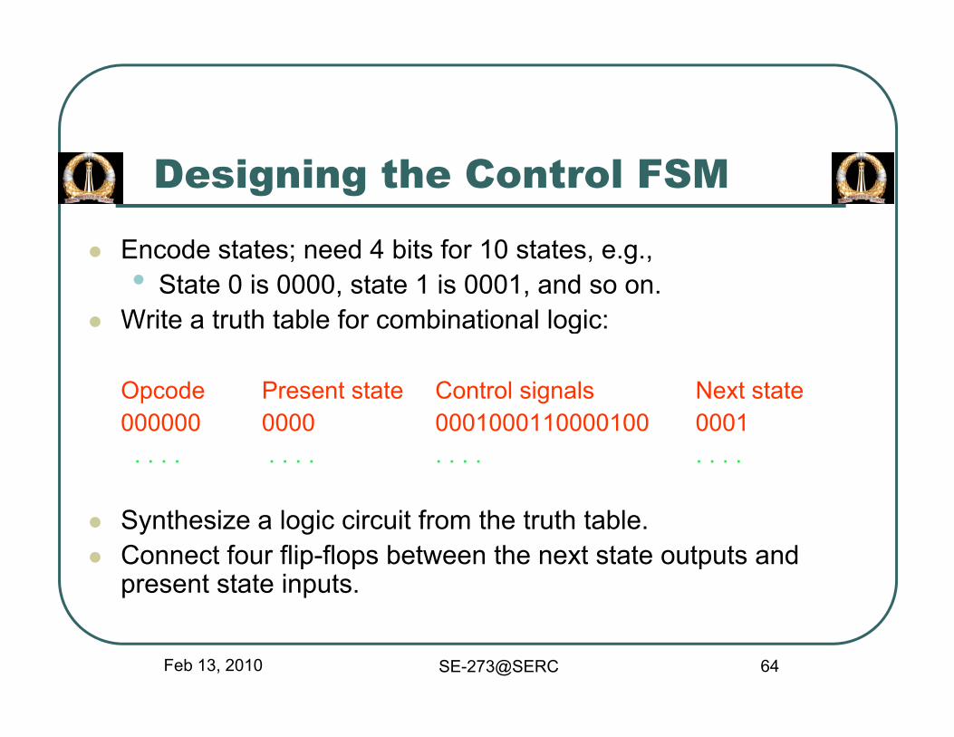
Designing the Control FSM
Encode states; need 4 bits for 10 states, e.g.,• State 0 is 0000, state 1 is 0001, and so on.
Write a truth table for combinational logic:Write a truth table for combinational logic:
Opcode Present state Control signals Next state000000 0000 0001000110000100 0001000000 0000 0001000110000100 0001. . . . . . . . . . . . . . . .
Synthesize a logic circuit from the truth table.Connect four flip-flops between the next state outputs and present state inputs.
Feb 13, 2010 SE-273@SERC 64
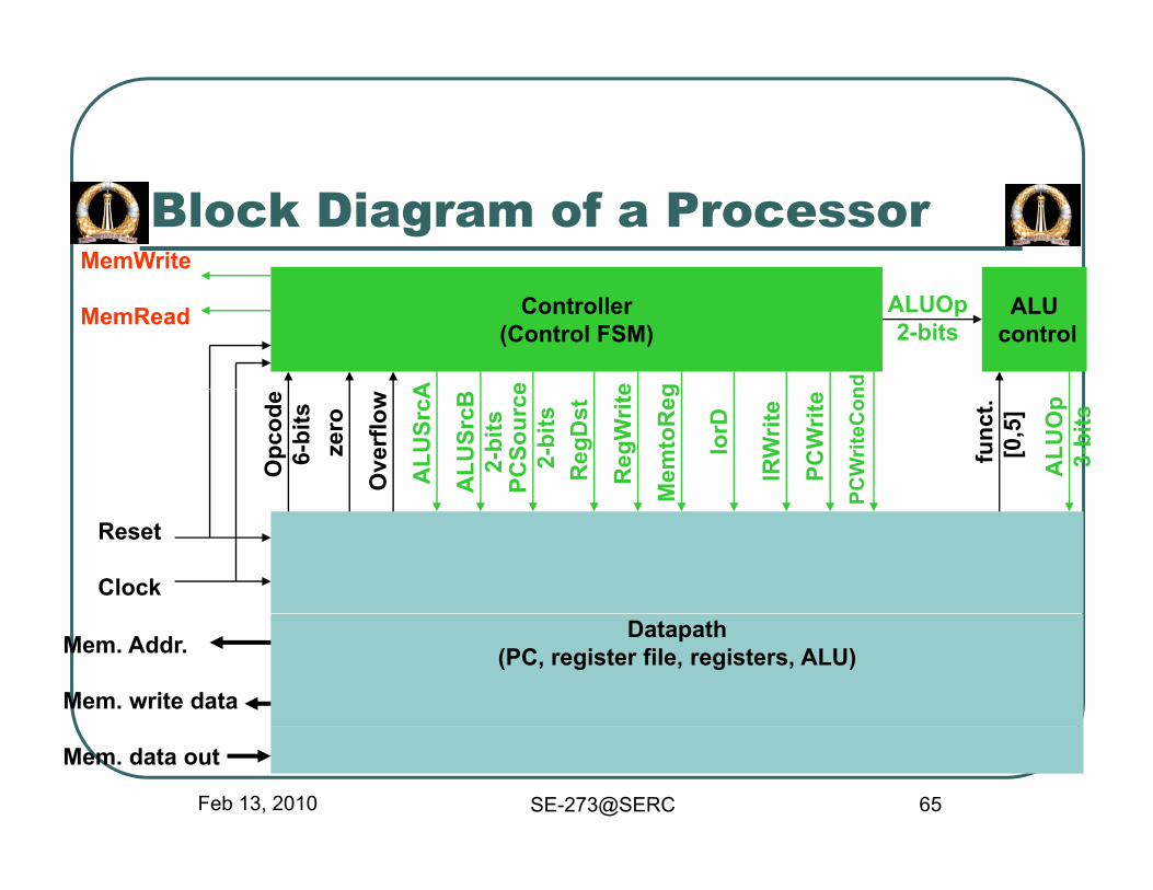
Block Diagram of a ProcessorMemWrite
Controller(Control FSM)
ALUcontrol
MemRead ALUOp2-bits
A e e g nd
func
t.[0
,5]
ALU
Op
3-bi
ts
Opc
ode
6-bi
tsze
ro
Ove
rflo
w
ALU
SrcA
ALU
SrcB
2-bi
tsPC
Sour
ce2-
bits
Reg
Dst
Reg
Writ
e
Mem
toR
eg
IorD
IRW
rite
PCW
rite
PCW
riteC
on
Reset
Clock
P
Datapath(PC, register file, registers, ALU)Mem. Addr.
Mem. write data
Feb 13, 2010 SE-273@SERC 65
Mem. data out

Exceptions or InterruptsC diti d hi h thConditions under which the processor may produce incorrect result or may “hang”.• Illegal or undefined opcode.g p• Arithmetic overflow, divide by zero, etc.• Out of bounds memory address.
EPC 32 bit register holds the affected instr ctionEPC: 32-bit register holds the affected instruction address.Cause: 32-bit register holds an encoded exceptionCause: 32 bit register holds an encoded exception type. For example,• 0 for undefined instruction• 1 f ith ti fl
Feb 13, 2010 SE-273@SERC 66
• 1 for arithmetic overflow
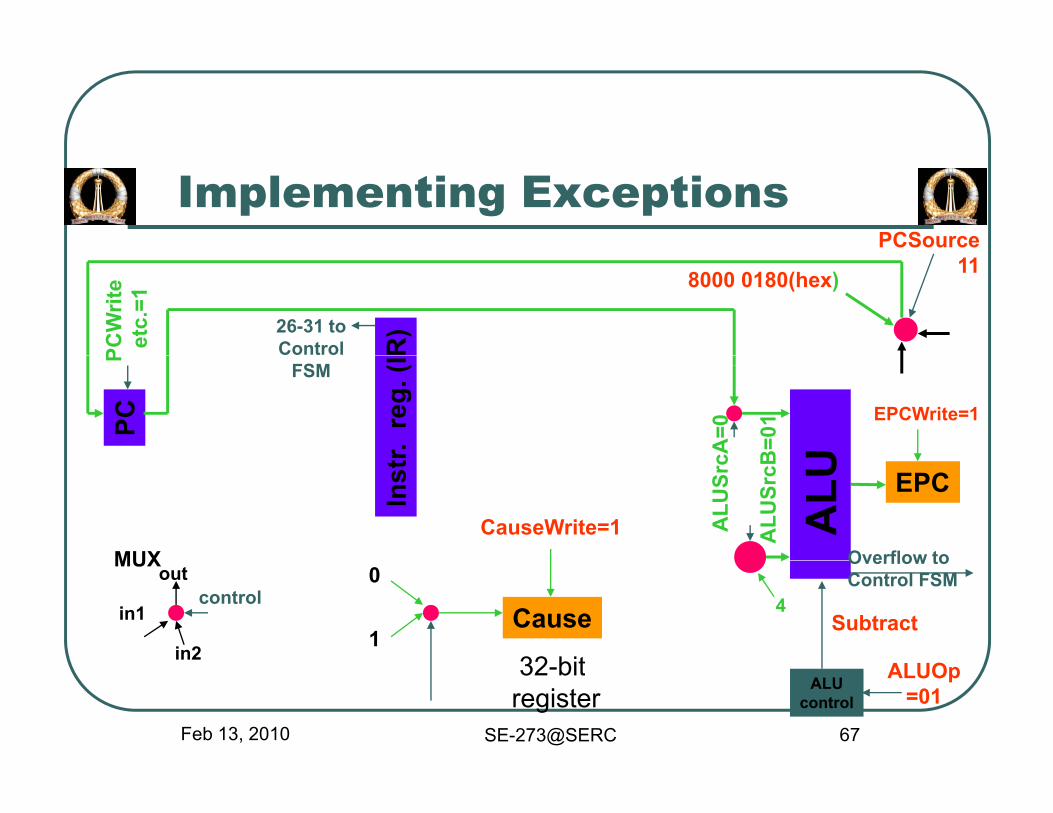
Implementing ExceptionsPCSource
R)
11
PCW
rite
etc.
=1
26-31 toControl
8000 0180(hex)
PC
r. re
g. (I
B=0
1
cA=0
P
FSM
U
EPCWrite=1In
st
ALU
SrcB
ALU
Src
MUX
ALU EPC
CauseWrite=1Overflow to
4
ALUO
in1
in2
outcontrol
MUX
SubtractCause0
1
Overflow toControl FSM
32 bit
Feb 13, 2010 SE-273@SERC 67
ALUcontrol
ALUOp=01
32-bitregister
How Long Does It Take? Again
Assume control logic is fast and does not affect the critical timing. Major time components are ALU, memory read/write, and register read/write.Time for hardware operations, suppose
• Memory read or write 2ns• Register read 1ns• ALU operation 2ns• Register write 1ns
Feb 13, 2010 SE-273@SERC 68
Register write 1ns

Single-Cycle Datapath
R-type 6nsLoad word (I-type) 8ns( yp )Store word (I-type) 7nsBranch on equal (I-type) 5nsBranch on equal (I-type) 5nsJump (J-type) 2nsCl k l ti 8Clock cycle time = 8nsEach instruction takes one cycle
Feb 13, 2010 SE-273@SERC 69
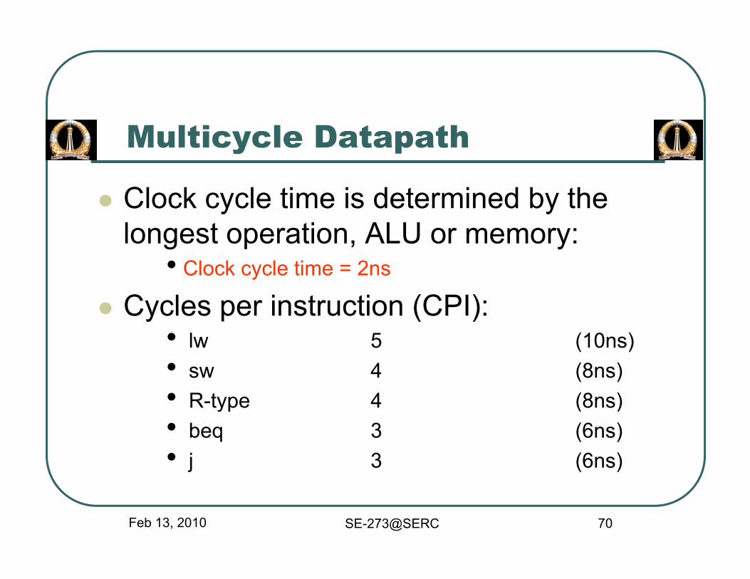
Multicycle Datapath
Clock cycle time is determined by the longest operation, ALU or memory:
• Clock cycle time = 2ns
Cycles per instruction (CPI):• lw 5 (10ns)• sw 4 (8ns)• R type 4 (8ns)• R-type 4 (8ns)• beq 3 (6ns)• j 3 (6ns)
Feb 13, 2010 SE-273@SERC 70
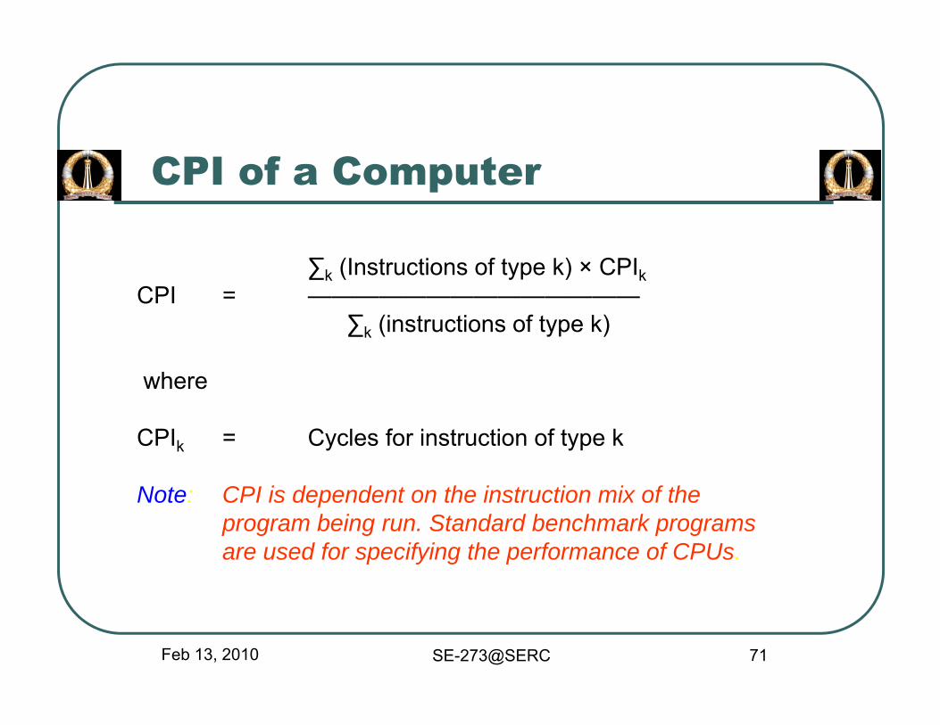
CPI of a Computer
∑k (Instructions of type k) × CPIkCPI = ——————————————
∑ (i t ti f t k)∑k (instructions of type k)
where
CPIk = Cycles for instruction of type k
Note: CPI is dependent on the instruction mix of theNote: CPI is dependent on the instruction mix of theprogram being run. Standard benchmark programsare used for specifying the performance of CPUs.
Feb 13, 2010 SE-273@SERC 71

ExampleC id t i iConsider a program containing:
• loads 25%• stores 10%stores 10%• branches 11%• jumps 2%• Arithmetic 52%• Arithmetic 52%
CPI = 0.25×5 + 0.10×4 + 0.11×3 + 0 02×3 + 0 52×40.02×3 + 0.52×4
= 4.12 for multicycle datapathCPI = 1 00 for single cycle datapath
Feb 13, 2010 SE-273@SERC 72
CPI = 1.00 for single-cycle datapath
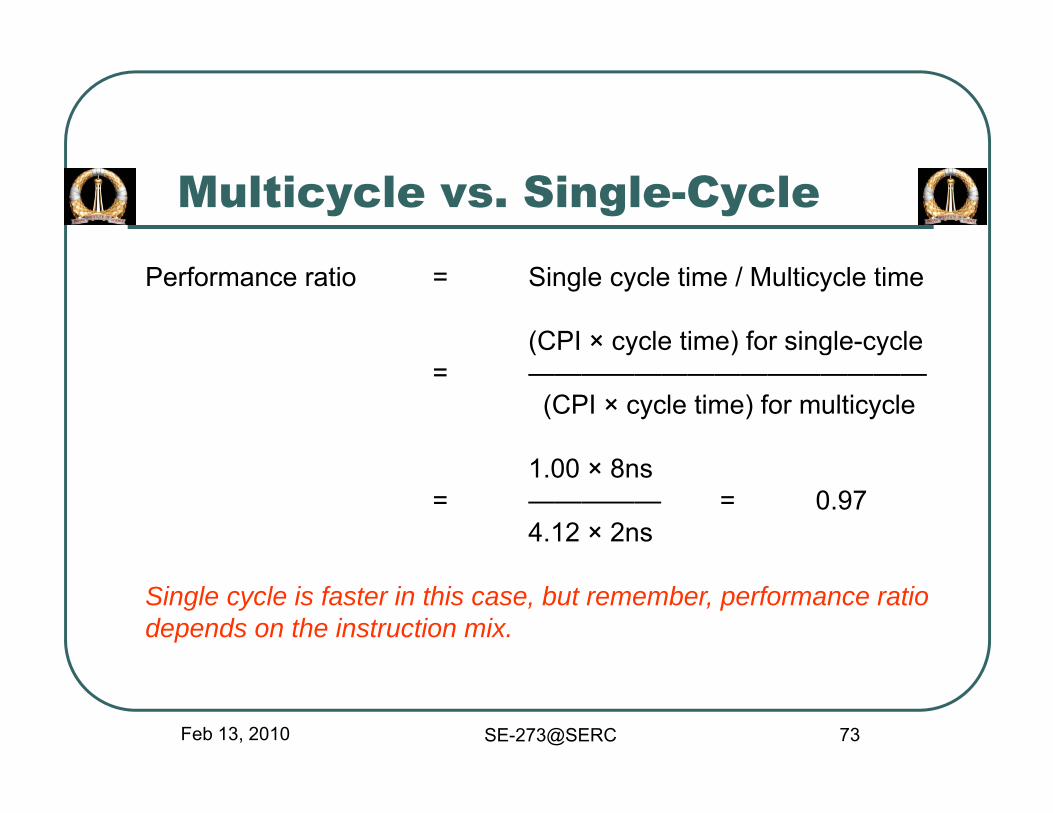
Multicycle vs. Single-Cycle
Performance ratio = Single cycle time / Multicycle time
(CPI × cycle time) for single-cycle= ———————————————
(CPI × cycle time) for multicycle
1.00 × 8ns= ————— = 0.97
4.12 × 2ns
Single cycle is faster in this case, but remember, performance ratiodepends on the instruction mix.
Feb 13, 2010 SE-273@SERC 73
Thank YouThank You
Feb 13, 2010 SE-273@SERC 74