risc processor background - altiumvalhalla.altium.com/learning-guides/legacy/cr0121 tsk3000a 32...
TRANSCRIPT

Legacy documentation refer to the Altium Wiki for current information
TSK3000A 32-bit RISC Processor
Summary Core Reference CR0121 (v3.0) March 19, 2008
The TSK3000A is a fully functional, 32-bit load/store, Wishbone-compliant processor that employs RISC architecture with a streamlined set of single word instructions. This core reference includes architectural and hardware descriptions, instruction sets and on-chip debugging functionality for the TSK3000A.
The TSK3000A is a 32-bit, Wishbone-compatible, RISC processor. Most instructions are 32-bits wide and execute in a single clock cycle. In addition to fast register access, the TSK3000A features a user-definable amount of zero-wait state block RAM, with true dual-port access.
The TSK3000A has been specifically designed to simplify the development of 32-bit systems targeted for FPGA implementation and to allow the migration of existing 8-bit systems to the 32-bit domain with relative ease and low-risk. As a result, complications typically associated with 32-bit system design, such as complex memory management, are minimized.
The TSK3000A, although a “classic RISC” processor and internally based on the Harvard architecture, features a greatly simplified memory structure and sophisticated interrupt handling to make coding simpler. The processor also simplifies the connection of peripherals with support for the Wishbone microprocessor bus.
The TSK3000A can be used with any FPGA device of suitable capacity supported by Altium Designer, giving a completely device and FPGA vendor-independent 32-bit system hardware platform.
Features • 5-stage pipelined RISC processor
• 32x32- to 64-bit hardware multiplier, signed and unsigned
• 32x32-bit hardware divider
• 32-bit single-cycle barrel shifter
• 32 input interrupts, individually configurable to be level or edge sensitive and used in one of two modes:
- Standard Mode - all interrupts jump to the same, configurable base vector
- Vectored Mode - providing 32 vectored priority interrupts, each jumping to a separate interrupt vector
• Internal Harvard architecture with simplified external memory access
• 4GByte address space
• Wishbone I/O and memory ports for simplified peripheral connection
• Full Viper-based software development tool chain – C compiler/assembler/source-level debugger/profiler
• C-code compatible with other Altium Designer 8-bit and 32-bit Wishbone-compliant processor cores, for easy design migration
• FPGA device-independent implementation
Available Devices The TSK3000A device can be found in the FPGA Processors integrated library (FPGA Processors.IntLib), located in the \Library\Fpga folder of the installation.
CR0121 (v3.0) March 19, 2008 1

Legacy documentation refer to the Altium Wiki for current information
TSK3000A 32-bit RISC Processor
RISC Processor Background RISC, or Reduced Instruction Set Computer, is a term that is conventionally used to describe a type of microprocessor architecture that employs a small but highly-optimized set of instructions, rather than the large set of more specialized instructions often found in other types of architectures. This other type of processor is traditionally referred to as CISC, or Complex Instruction Set Computer.
History The early RISC processors came from research projects at Stanford and Berkeley universities in the late 1970s and early 1980s. These processors were designed with a similar philosophy, which has become known as RISC. The basic design architecture of all RISC processors has generally followed the characteristics that came from these early research projects and which can be summarized as follows: • One instruction per clock cycle execution time: RISC processors have a CPI (clock per instruction) of one cycle. This is
due to the optimization of each instruction on the CPU and a technique called pipelining. This technique allows each instruction to be processed in a set number of stages. This in turn allows for the simultaneous execution of a number of different instructions, each instruction being at a different stage in the pipeline.
• Load/Store machine with a large number of internal registers: The RISC design philosophy typically uses a large number (commonly 32) of registers. Most instructions operate on these registers, with access to memory made using a very limited set of Load and Store instructions. This limits the need for continuous access to slow memory for loading and storing data.
• Separate Data Memory and Instruction Memory access paths: Different stages of the pipeline perform simultaneous accesses to memory. This Harvard style of architecture can either be used with two completely different memory spaces, a single dual-port memory space or, more commonly, a single memory space with separate data and instruction caches for the two pipeline stages.
Over the last 20-25 years, RISC processors have been steadily improved and optimized. In one sense, the original simplicity of the RISC architecture has been lost – replaced by super-scalar, multiple-pipelined hardware, often running in the gigahertz range.
“Soft” FPGA Processors With the advent of low-cost, high-capacity programmable logic devices, there has been something of a resurgence in the use of processors with simple RISC architectures. Register-rich FPGAs, with their synchronous design requirements, have found the ideal match when paired with these simple pipelined processors.
As a result, most 32-bit FPGA soft processors are adopting this approach. They could even be considered as “Retro-processors”.
Why use “Soft” Processors? There are a number of benefits to be gained from using soft processors on reconfigurable hardware. The following sections explore some of the more significant of these benefits in more detail.
Field Reconfigurable Hardware For certain specific applications, the ability to change the design once it is in the field can be a significant competitive advantage. Applications in general can benefit from this ability also. It allows commitment to shipping early in the development cycle. It also allows field testing to be used to help drive the latter part of the design cycle without requiring new “board-spins” based on the outcome. This is very similar to the way in which alpha, beta, pre-release and release cycles currently drive the closure of software products.
The ability to update embedded software in a device in the field has long been an advantage enjoyed by designers of embedded systems. With FPGAs, this has now become a reality for the hardware side of the design. For end-users, this translates as “Field Upgradeable Hardware”.
Faster Time to Market FPGAs offer the fastest time to market due to their programmable nature. Design problems, or feature changes, can be made quickly and simply by changing the FPGA design – with no changes in the board-level design.
2 CR0121 (v3.0) March 19, 2008

Legacy documentation refer to the Altium Wiki for current information
TSK3000A 32-bit RISC Processor
Improving and Extending Product Life-Cycles Fast time to market is usually synonymous with a weaker feature set – a traditional trade-off. With FPGA-based system designs you can have the best of both worlds. You can get your product to market quickly with a limited feature set, then follow-up with more extensive features over time, upgrading the product while it is already in the field.
This not only extends product life-cycles but also lowers the risk of entry, allowing new protocols to be added dynamically and hardware bugs to be fixed without product RMA.
Creating Application-Specific Coprocessors Algorithms can easily be moved between hardware and software implementations. This allows the design to be initially implemented in software, later off-loading intensive tasks into dedicated hardware, in order to meet performance objectives. Again, this can happen even after commitment to the board-level design.
Implementing Multiple Processors within a Single Device Extra processors can be added within a single FPGA device, simply by modifying the design with which the device is programmed. Once again, this can be achieved after the board-level design has been finalized and a commitment to production made.
Lowering System Cost Processors, peripherals, memory and I/O interfaces can be integrated into a single FPGA device, greatly reducing system complexity and cost. Once the FPGA-based embedded application moves to 32-bit, cost becomes an even more powerful driver.
As large FPGAs become cheaper, both Hybrids and soft cores move into the same general cost area as dedicated processors. At the heart of this argument is also the idea that once you have paid for the FPGA, any extra IP that you place in the device is free functionality.
Avoiding Processor Obsolescence As products mature, processor supply may become an increasing problem, particularly where the processor is one of many variants supplied by the semiconductor vendor. Switching to a new processor usually requires design software changes or logical hardware changes.
With FPGA implementations, the design can be easily moved to a different device with little or no change to the hardware logic and probably no change to the application software. Peripherals are created dynamically in the hardware, so lack of availability of specific processor variants is never a problem.
The TSK3000A The TSK3000A is a 32-bit RISC machine that follows the classic RISC architecture previously described. It is a load/store machine with 32 general purpose registers.
Most instructions are 32-bits wide and execute in a single clock cycle.
In addition to fast register access the TSK3000A, relying on the commonly available fast block RAM in FPGA devices, also features a user-definable amount of zero-wait state block RAM, with true dual-port access.
Wishbone Bus Interfaces The TSK3000A has been built to use the Wishbone bus standard. This standard is formally described as a “System-on-Chip Interconnection Architecture for Portable IP Cores”. The current standard is the Revision B.3 Specification, a copy of which is included as part of the software installation and can be found by navigating to the Documentation Library » Designing with FPGAs section of the Knowledge Center panel.
The Wishbone standard is not copyrighted and resides in the public domain. It may be freely copied and distributed by any means. Furthermore, it may be used for the design and production of integrated circuit components without royalties or other financial obligations. It is also implicitly device and vendor independent, making it very simple to create highly portable designs.
Wishbone OpenBUS Processor Wrappers To normalize access to hardware and peripherals, each of the 32-bit processors supported in Altium Designer has a Wishbone OpenBUS-based FPGA core that 'wraps' around the processor. This enables peripherals defined in the FPGA to be used transparently with any type of processor. An FPGA OpenBUS wrapper around discrete, hard-wired peripherals also allows them to be moved seamlessly between processors.
CR0121 (v3.0) March 19, 2008 3

Legacy documentation refer to the Altium Wiki for current information
TSK3000A 32-bit RISC Processor
The OpenBUS wrappers can be implemented in any FPGA and allow the designer to implement FPGA-based portable cores, taking advantage of the device driver system in Altium Designer for both FPGA-based soft-core peripherals as well as connections to off-chip discrete peripherals and memory devices.
Processor Abstraction System Use of OpenBUS wrappers creates a plug-in processor abstraction system that normalizes the interface to interrupt systems and other hardware specific elements. The system provides an identical interface to the processor's interrupt system, whether soft or hard-vectored. This allows different processors to be used transparently with identical source code bases.
Design Migration With each 32-bit processor encased in a Wishbone OpenBUS wrapper, an embedded software design can be seamlessly moved between soft-core processors, hybrid hard-core processors and discrete processors.
The Wishbone OpenBUS wrapper around the TSK3000A processor makes it architecturally similar to the other 32-bit processors included with Altium Designer, both in terms of its memory map and its pinout. This allows for easy migration from the TSK3000A to any of the following devices:
• PPC405A – 'hard' PowerPC® 32-bit RISC processor immersed on the Xilinx® Virtex®-II Pro.
• Nios® II - 32-bit RISC processor targeted to Altera FPGA platforms.
• MicroBlaze™ – 32-bit RISC processor targeted to Xilinx FPGA platforms.
• PPC405CR – AMCC® PowerPC 32-bit RISC Microprocessor.
• ARM®720T_LH79520 – Sharp Bluestreak® LH79520 with built-in ARM720T (32-bit RISC microprocessor).
Altium Designer also features Wishbone-compliant versions of its TSK52x 8-bit processor. These Wishbone variants, along with true C-code compatibility between these and the Nios II, allow designs to be easily moved between the 8- and 32-bit worlds.
For further information on the PPC405A, refer to the PPC405A 32-bit RISC Processor core reference.
For further information on the Nios II, refer to the Nios II 32-bit RISC Processor core reference.
For further information on the MicroBlaze, refer to the MicroBlaze 32-bit RISC Processor core reference.
For further information on the TSK52x, refer to the TSK52x MCU core reference.
4 CR0121 (v3.0) March 19, 2008

Legacy documentation refer to the Altium Wiki for current information
TSK3000A 32-bit RISC Processor
Architectural Overview
Symbol
Figure 1. TSK3000A symbol
Pin Description The pinout of the TSK3000A has not been fixed to any specific device I/O - allowing flexibility with user application. The TSK3000A contains only unidirectional pins (inputs or outputs).
Table 1. TSK3000A pin description
Name Type Polarity/Bus size
Description
Control Signals
CLK_I I Rise External (system) clock
RST_I I High External (system) reset
Interrupt Signals
INT_I I 32 Interrupt inputs. Each input can be configured to operate as level-sensitive or edge-triggered by clearing or setting the corresponding bit in the IMode register respectively. Interrupts can be configured in one of two modes – Standard or Vectored – determined by the VIE bit of the Status register (Status.9)
Wishbone External Memory Interface Signals
ME_STB_O O High Strobe signal. When asserted, indicates the start of a valid Wishbone data transfer cycle
ME_CYC_O O High Cycle signal. When asserted, indicates the start of a valid Wishbone bus cycle. This signal remains asserted until the end of the bus cycle, where such a cycle can include multiple data transfers
ME_ACK_I I High Standard Wishbone device acknowledgement signal. When this signal goes High, an external Wishbone slave memory device has finished execution of the requested action and the current bus cycle is terminated
ME_ADR_O O 32 Standard Wishbone address bus, used to select an address in a connected Wishbone slave memory device for writing to/reading from
CR0121 (v3.0) March 19, 2008 5

Legacy documentation refer to the Altium Wiki for current information
TSK3000A 32-bit RISC Processor
Name Type Polarity/Bus size
Description
ME_DAT_I I 32 Data received from an external Wishbone slave memory device
ME_DAT_O O 32 Data to be sent to an external Wishbone slave memory device
ME_SEL_O O 4 Select output, used to determine where data is placed on the ME_DAT_O line during a Write cycle and from where on the ME_DAT_I line data is accessed during a Read cycle. Each of the data ports is 32-bits wide with 8-bit granularity, meaning data transfers can be 8-, 16- or 32-bit. The four select bits allow targeting of each of the four active bytes of a port, with bit 0 corresponding to the low byte (7..0) and bit 3 corresponding to the high byte (31..24)
ME_WE_O O Level Write enable signal. Used to indicate whether the current local bus cycle is a Read or Write cycle.
0 = Read 1 = Write
ME_CLK_O O Rise External (system) clock signal (identical to CLK_I), made available for connecting to the CLK_I input of a slave memory device. Though not part of the standard Wishbone interface, this signal is provided for convenience when wiring your design
ME_RST_O O High Reset signal made available for connection to the RST_I input of a slave memory device. This signal goes High when an external reset is issued to the processor on its RST_I pin. When this signal goes Low, the reset cycle has completed and the processor is active again. Though not part of the standard Wishbone interface, this signal is provided for convenience when wiring your design
Wishbone Peripheral I/O Interface Signals
IO_STB_O O High Strobe signal. When asserted, indicates the start of a valid Wishbone data transfer cycle
IO_CYC_O O High Cycle signal. When asserted, indicates the start of a valid Wishbone bus cycle. This signal remains asserted until the end of the bus cycle, where such a cycle can include multiple data transfers
IO_ACK_I I High Standard Wishbone device acknowledgement signal. When this signal goes High, an external Wishbone slave peripheral device has finished execution of the requested action and the current bus cycle is terminated
IO_ADR_O O 24 Standard Wishbone address bus, used to select an internal register of a connected Wishbone slave peripheral device for writing to/reading from
IO_DAT_I I 32 Data received from an external Wishbone slave peripheral device
IO_DAT_O O 32 Data to be sent to an external Wishbone slave peripheral device
IO_SEL_O O 4 Select output, used to determine where data is placed on the IO_DAT_O line during a Write cycle and from where on the IO_DAT_I line data is accessed during a Read cycle. Each of the data ports is 32-bits wide with 8-bit granularity, meaning data transfers can be 8-, 16- or 32-bit. The four select bits allow targeting of each of the four active bytes of a port, with bit 0 corresponding to the low byte (7..0) and bit 3 corresponding to the high byte (31..24)
IO_WE_O O Level Write enable signal. Used to indicate whether the current local bus cycle is a Read or Write cycle.
0 = Read 1 = Write
IO_CLK_O O Rise External (system) clock signal (identical to CLK_I), made available for connecting to the CLK_I input of a slave peripheral device. Though not part of the standard Wishbone interface, this signal is provided for convenience when wiring your design
IO_RST_O O High Reset signal made available for connection to the RST_I input of a slave peripheral device. This signal goes High when an external reset is issued to the processor on its RST_I pin. When this signal goes Low, the reset cycle has completed and the processor is active again. Though not part of the standard Wishbone interface, this signal is provided for convenience when wiring your design
6 CR0121 (v3.0) March 19, 2008

Legacy documentation refer to the Altium Wiki for current information
TSK3000A 32-bit RISC Processor
Configuring the Processor from the Schematic Design The architecture of the TSK3000A can be configured after placement on the schematic sheet. Simply right-click and choose the command to configure the processor from the pop-up menu that appears (e.g. Configure U_MCU1 (TSK3000A) for a processor with designator U_MCU1). Alternatively, click on the Configure button, available in the Component Properties dialog for the processor.
The Configure (32-bit Processors) dialog will appear as shown in . Figure 2
Figure 2. Options to configure the architecture of the TSK3000A
The drop-down field at the top-right of the dialog enables you to choose the type of processor you want to work with. As the pinouts between the 32-bit processors are essentially the same, you can easily change the processor used in your design without having to extensively rewire the external interfaces.
As you select the processor type, the Configure (32-bit Processors) dialog will change accordingly to reflect the architectural options available. The symbol on the schematic will also change to reflect the type of processor and configuration options chosen.
The following sections explore each of the regions in the dialog, providing configurable options specific to the TSK3000A processor.
Internal Processor Memory This region of the dialog allows you to define the size of the internal memory for the processor. This memory, also referred to as ‘Low’ or ‘Boot’ memory is implemented using true dual port FPGA Block RAM and will contain the boot part of a software application and the interrupt and exception handlers.
Speed-critical (or latency-sensitive) parts of an application should also be placed in this memory space.
The following memory sizes are available to choose from: • 1KB (256 x 32-bit Words)
• 2KB (512 x 32-bit Words)
• 4KB (1K x 32-bit Words)
• 8KB (2K x 32-bit Words)
• 16KB (4K x 32-bit Words)
• 32KB (8K x 32-bit Words)
• 64KB (16K x 32-bit Words)
• 128KB (32K x 32-bit Words)
• 256KB (64K x 32-bit Words)
• 512KB (128K x 32-bit Words)
CR0121 (v3.0) March 19, 2008 7

Legacy documentation refer to the Altium Wiki for current information
TSK3000A 32-bit RISC Processor
• 1MB (256K x 32-bit Words).
Your configuration choice will be reflected in the Current Configuration region of the processor's schematic symbol (Figure 3).
Multiply/Divide Unit (MDU) This region of the dialog allows you to define whether the processor should incorporate an MDU or not. Either choose to include an MDU in the architecture by selecting the Hardware MDU option, or leave the MDU out of the architecture by choosing No MDU Hardware.
Figure 3. Current configuration settings for the processor.
With no MDU included in the architecture, the multiply (MULT, MULTU) and divide (DIV, DIVU) hardware instructions will not be available and these instructions will be emulated in software by the C Compiler. Your configuration choice will be reflected in the Current Configuration region of the processor’s schematic symbol (Figure 3).
On-Chip Debug System This region of the dialog allows you to add an On-Chip Debug System (OCDS) unit to the processor’s architecture, allowing you to: • control the processor from its associated instrument panel, which can be added to the Instrument Rack – Soft Devices
panel
• interrogate and modify memory and register values in real-time
• perform source level debugging of the embedded software application running on the processor. Simply ensure that the option is set to Include JTAG-Based On-Chip Debug System.
For further information with respect to real-time debugging of the processor, refer to the On-Chip Debugging section of this reference.
By specifying No On-Chip Debug System for the processor, the above capabilities will be removed, but the processor will naturally consume less FPGA resources. Again, your configuration choice will be reflected in the Current Configuration region of the processor’s schematic symbol (Figure 3).
Breakpoints on Reset This region of the dialog allows you to specify whether debugging of the processor from a Hard Reset is enabled or not. If you choose the option to Enable Breakpoints on Hard Reset, then the processor will stop upon encountering a breakpoint immediately after an external reset is received on its RST_I input pin.
8 CR0121 (v3.0) March 19, 2008

Legacy documentation refer to the Altium Wiki for current information
TSK3000A 32-bit RISC Processor
Memory & I/O Management The TSK3000A uses 32-bit address buses providing a 4GByte linear address space. All memory access is in 32-bit words, which creates a physical address bus of 30-bits.
Memory space is broken into three main areas, as illustrated in Figure 4 and described in the section – Division of Memory Space.
Before detailing the nature of each of these memory regions, it is worthwhile discussing the difficulties with mapping devices into this memory, and the solution that Altium Designer brings to the problem.
0000_0000h
00FF_FFFFh0100_0000h
FEFF_FFFFh
FFFF_FFFFh
FF00_0000hPeripheral I/O
External Memory
Internal Memory
Figure 4. Memory organization in the TSK3000A
Defining the Memory Map An area that can be difficult to manage in an embedded software development project is the mapping of memory and peripherals into the processor’s address space.
The memory map, as it is often called, is essentially the bridge between the hardware and software projects – the hardware team allocating each of the various memory and peripheral devices their own chunk of the processor’s address space, the software team then writing their code to access the memory and peripherals at the given locations.
To help manage the process of allocating devices into the space there are a number of features available to both the hardware designer and the embedded software developer in Altium Designer.
This discussion is based around the TSK3000A processor, however the overall approach can be applied to any of the 32-bit processors available in Altium Designer.
Building the Bridge between the Hardware and Software Defining the memory map on the hardware (FPGA project) side is essentially a 3 stage process:
• Place the peripheral or memory
• Define its addressing requirements (this is most easily done using a Wishbone Interconnect device)
• Bring that definition into the processor’s configuration, which can then be accessed by the embedded tools
Figure 5 shows an example of the addressable memory and IO space for the TSK3000A, with a number of memory and peripheral devices mapped into it.
CR0121 (v3.0) March 19, 2008 9

Legacy documentation refer to the Altium Wiki for current information
TSK3000A 32-bit RISC Processor
Figure 5. The TSK3000A’s 232 addressable space (left) and the current set of memory and peripheral devices that have been mapped into it (right)
10 CR0121 (v3.0) March 19, 2008

Legacy documentation refer to the Altium Wiki for current information
TSK3000A 32-bit RISC Processor
The adjacent flow chart shows the process that was followed to build this memory map in the FPGA project. This flow chart is only a guide, during the course of development it is likely that you will jump back and forth through this process as you build up the design.
Place Processor
Place WishboneInterconnect
Configure Processorto see Peripherals(import settings from WB
intercon)
Peripheral memorymap ready for
embedded project(repeat process for
memory)
(peripheral n) (peripheral 2)
Place peripheralcomponent on
schematic (peripheral 1)
(Add and Setup Pn)
(Add and Setup P2)
ConfigureWishbone
Interconnect (Add and Setup P1)
The flow of connecting and mapping the peripherals (or memory) to the processor
Dedicated System Interconnect Components This process of being able to quickly build up the design and resolve the processor to memory & peripheral interface is possible because of the specialized interconnection components, including the Wishbone Interconnect, the Wishbone Dual Master and the Wishbone Multi-Master. These three components solve the common system interconnect issues that face the designer, these being:
• Interfacing multiple peripheral and memory blocks to a processor (handled by the Wishbone Interconnect component)
• Allowing two or more system components, that must each be able to control the bus, to share access to a common resource (provided by the Wishbone Dual Master or Wishbone Multi-Master components).
Use of the Wishbone Interconnection Architecture for all part s of the system that connect to the processor contributes to the system’s ‘building block’ behavior. The Wishbone standard resolves data exchange between system components – supporting popular data transfer bus protocols, while defining clocking, handshaking and decoding requirements (amongst others).
With the lower-level physical interface requirements being resolved by the Wishbone interface, the other challenge is the structural aspects of the system – defining where components sit in the address space, providing address decoding, and allocating and interfacing interrupts to the processor.
For more information on the Wishbone Interconnect component, refer to the WB_INTERCON Configurable Wishbone Interconnect core reference.
For more information on the Wishbone Dual Master component, refer to the WB_DUALMASTER Configurable Wishbone Dual Master core reference.
For more information on the Wishbone Multi-Master component, refer to the WB_MULTIMASTER Configurable Wishbone Multi-Master core reference.
Configuring the Processor Each configurable component has its own configuration dialog, including the different processors. The processor has separate commands and dialogs to configure memory and peripherals, but it does support mapping peripherals into memory space (and the memory into peripheral space), if required. An important feature to point out is the Import from Schematic button in the processor’s Configure dialogs, clicking this will read in the settings from the Interconnects attached to the processor. This lets you quickly build the memory map, as shown in the figure earlier. You now have the memory map defined in the hardware, this data is stored with the processor component.
The processor’s Configure dialogs includes options to generate assembler and C hardware description files that can be included in your embedded project, simplifying the task of declaring peripheral and memory structures in your embedded code. You can also ‘pull’ the memory map configurations directly into the embedded project by enabling the Automatically import when compiling FPGA project option in the Configure Memory tab of the Options for Embedded Project dialog.
For more information on mapping physical memory devices and I/O peripherals into the processor's address space, refer to the application note Allocating Address Space in a 32-bit Processor.
Division of Memory Space As illustrated previously (Figure 4), the TSK3000A'S 4GB address space is divided into three distinct areas (or ranges). These areas are detailed in the following sections.
Internal Memory The internal "Low" or "Boot" RAM is contained within the processor core and is built using true dual-port FPGA block RAM memory. As such, it can be read or written on both sides, simultaneously, in a single cycle.
CR0121 (v3.0) March 19, 2008 11

Legacy documentation refer to the Altium Wiki for current information
TSK3000A 32-bit RISC Processor
This memory still has the standard limitation of load delay slots, because the load from memory happens further down the pipeline, after the Execute stage. As a result, any operation that requires loaded data in the cycle immediately after the load will cause the processor to insert a load stall, holding the first half of the pipeline for one cycle while the data becomes available.
Other than this single limitation, the RAM block is as fast as the internal processor registers themselves.
The size of the RAM can vary between 1KB and 16MB, dependent on the availability of embedded block RAM in the physical FPGA device used. Memory size is configured in the Internal Processor Memory region of the Configure (32-bit Processors) dialog (see the Internal Processor Memory section).
Covering the processor's address space between 0000_0000h and 00FF_FFFFh, it will contain the reset and interrupt vectors, as well as any speed or latency-sensitive code or data.
External Memory The processor's Wishbone External Memory Interface is used by both the instruction and data sides of the processor and provides access to the majority of the address space of the processor. It covers the address space between 0100_0000h and FF00_0000h – 1.
There are no caches on external memory.
External Memory Interface Time-out A simple time-out mechanism for the interface handles the case when attempting to access an address that does not exist, or if the addressed target slave device is not operating correctly. This mechanism ensures that the processor will not be ‘locked’ indefinitely, waiting for an acknowledgement on its ME_ACK_I input.
After the ME_STB_O output is taken High, the processor will wait 4096 cycles of the external clock signal (CLK_I) for an acknowledge signal to appear from the addressed slave memory device, before forcibly terminating the current data transfer cycle.
If a time-out occurs, the ACK bit of the Status register (Status.10) will be taken High. This can be cleared to zero under software control to allow for detection of further Wishbone time-outs.
The ACK_O signal from a slave device should not be used as a ‘long delay’ hand-shaking mechanism. Where such a mechanism needs to be implemented, either use polling or interrupts.
Peripheral I/O The processor's Wishbone Peripheral I/O Interface is a one-way Wishbone Master, handling I/O in a very similar way to external memory. The port can be used to communicate with any Wishbone Slave peripheral device and covers the address space between FF00_0000h and FFFF_FFFFh. This address space of 16MB allows a physical address bus size of 24 bits.
Peripheral I/O Interface Time-out A simple time-out mechanism for the interface handles the case when attempting to access an address that does not exist, or if the addressed target slave device is not operating correctly. This mechanism ensures that the processor will not be ‘locked’ indefinitely, waiting for an acknowledgement on its IO_ACK_I input.
After the IO_STB_O output is taken High, the processor will wait 4096 cycles of the external clock signal (CLK_I) for an acknowledge signal to appear from the addressed slave peripheral device, before forcibly terminating the current data transfer cycle.
If a time-out occurs, the ACK bit of the Status register (Status.10) will be taken High. This can be cleared to zero under software control to allow for detection of further Wishbone time-outs.
The ACK_O signal from a slave peripheral should not be used as a ‘long delay’ hand-shaking mechanism. Where such a mechanism needs to be implemented, either use polling or interrupts.
For more information on connection of slave physical memory and peripheral I/O devices to the processor's Wishbone interfaces, refer to the application note Connecting Memory and Peripheral Devices to a 32-bit Processor.
Data Organization Data organization refers to the ordering of the data during transfers. There are two general types of ordering: • BIG ENDIAN – the most significant portion of an operand is stored at the lower address
• LITTLE ENDIAN – the most significant portion of an operand is stored at the higher address.
Although the Wishbone specification supports both of these methods for ordering data, the TSK3000A is always BIG ENDIAN.
12 CR0121 (v3.0) March 19, 2008

Legacy documentation refer to the Altium Wiki for current information
TSK3000A 32-bit RISC Processor
Words, Half-Words and Bytes The TSK3000A operates on the following data sizes:
• 32-bit words
• 16-bit half-words
• 8-bit bytes.
There are dedicated load and store instructions for these three data types.
Figure 6
Figure 6. Organization of data types for the TSK3000A
shows how these different sizes of data are organized relative to each other over an 8-byte memory range in the TSK3000A.
Word-0 Word-1
31 24 23 16 15 8 7 0 31 24 23 16 15 8 7 0
Half-0 Half-1 Half-2 Half-3
15 8 7 0 15 8 7 0 15 8 7 0 15 8 7 0
Byte-0 Byte-1 Byte-2 Byte-3 Byte-4 Byte-5 Byte-6 Byte-7
7 0 7 0 7 0 7 0 7 0 7 0 7 0 7 0
Physical Interface to Memory and Peripherals The TSK3000A's physical interface to the outside world is always 32 bits wide. Since the addressing has a byte-level resolution, this means that up to four "packets" of data (bytes) can be loaded or stored during a single memory access. To accommodate this requirement all memory accesses (8-bit, 16-bit and 32-bit) are handled in a specific way.
Each 32-bit read and write can be considered as a read or write through four "byte-lanes". These byte-lanes are marked as valid by the corresponding bits in the SEL_O[3..0] signal of the relevant Wishbone interface (External Memory or Peripheral I/O). Each of these bits will be High if the byte data in that lane is valid. This allows a single byte to be written to 32-bit wide memory without needing to use a slower read-modify-write cycle.
The instructions of the TSK3000A require that all 32-bit load/store operations be aligned on 4-byte boundaries and all 16-bit load/store operations be aligned on 2-byte boundaries. Byte operations (8-bit) can be to any address.
To complete a byte load or store, the TSK3000A will position the byte data in the correct byte-lane and set the SEL_O signal for that lane High. The memory hardware must then only enable writing on the relevant 8-bits of data from the 32-bit word.
When reading, the TSK3000A will put the relevant 8- or 16-bit value into the LSB's of the 32-bit word. What happens with the remaining bits depends on the operation:
• for an unsigned read, the processor will pad-out the remaining 24 or 16 bits respectively with zeroes
• for a byte load/store, the processor will sign-extend from bit 8
• for a half-word load/store, the processor will sign-extend from bit 16.
Peripheral I/O For memory I/O the process described happens transparently, because memory devices are always seen by the processor as 32 bits wide. Even when connecting to small 8- or 16-bit physical memories, the interfacing Memory Controller device will, as far as the processor is concerned, make the memory look like it is 32 bits wide.
For peripheral devices, the process is not so simple. 32-bit wide peripheral devices behave like memory devices, although they may or may not support individual byte-lanes. These devices should therefore be accessed using the 32-bit LW and SW instructions. For C-code, this means declaring the interface to the device as 32 bits wide, for example: #define Port32 (*(volatile unsigned int*) Port32_Address)
This will result in the software using LW and SW instructions to access the device.
If the 32-bit peripheral does support byte-lanes (i.e. it has a SEL_I[3..0] input), then smaller accesses can be performed using the 8-bit LBU and SB or 16-bit LHU and SH instructions.
CR0121 (v3.0) March 19, 2008 13

Legacy documentation refer to the Altium Wiki for current information
TSK3000A 32-bit RISC Processor
For smaller devices, there needs to be translation of the 8- or 16-bit values into the relevant byte-lanes in the processor. This is automatically handled by the Wishbone Interconnect device if it is used to access slave peripheral I/O devices. There is, however, some hardware penalty for this since it requires an extra 4:1 8-bit multiplexer for 8-bit devices or a 2:1 16-bit multiplexer for 16-bit devices.
16-bit peripheral devices should be accessed using the 16-bit LHU and SH instructions. For C-code, this means declaring the interface to the device as 16 bits wide, for example: #define Port16 (*(volatile unsigned short*) Port16_Address)
This will result in the software using LHU and SH instructions to access the device.
8-bit peripheral devices should be accessed using the 8-bit LBU and SB instructions. For C-code, this means declaring the interface to the device as 8 bits wide, for example: #define Port8 (*(volatile unsigned char*) Port8_Address)
This will result in the software using LBU and SB instructions to access the device.
There are some trade-offs that may need to be considered when deciding whether to use 8-, 16- or 32-bit wide devices. It may require significantly less hardware to implement a single 32-bit wide I/O port than it would to implement four separate 8-bit ports. If however, the natural format of the data packets is 8-bits and hardware size is not a constraint, then it may be better to use 8-bit ports since there will be no need to use software to break up a 32-bit value into smaller components.
If you are only accessing 8-bits at any one time, then software may also execute faster when using 8-bit wide peripherals, since there is need for extra instructions to extract the 8-bit values from the 32-bit values.
14 CR0121 (v3.0) March 19, 2008
Legacy documentation refer to the Altium Wiki for current information
TSK3000A 32-bit RISC Processor
Hardware Description
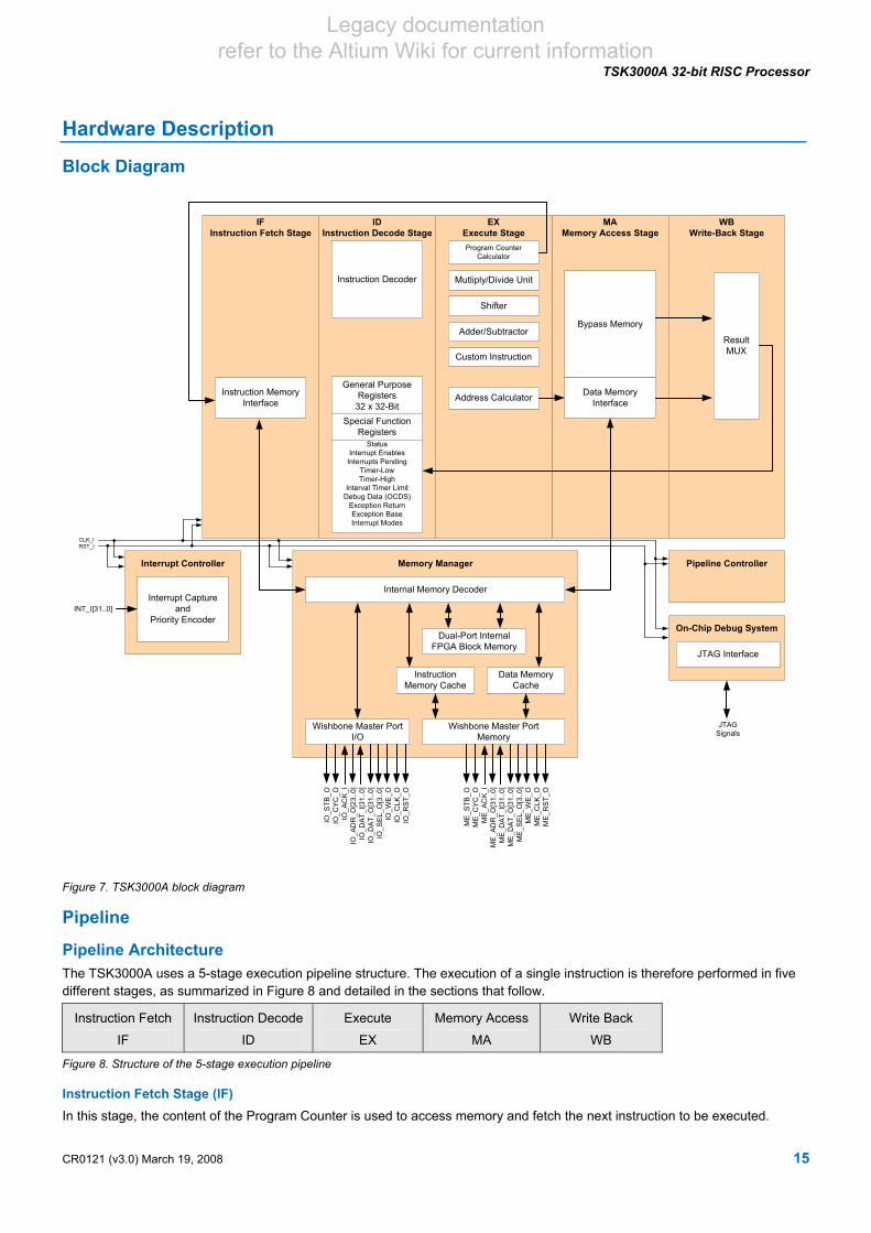
Block Diagram
StatusInterrupt Enables
Interrupts PendingTimer-LowTimer-High
Interval Timer LimitDebug Data (OCDS)
Exception ReturnException BaseInterrupt Modes
Bypass Memory
EXExecute Stage
Data MemoryInterface
MAMemory Access Stage
IDInstruction Decode Stage
Instruction Decoder
General PurposeRegisters
32 x 32-BitSpecial Function
Registers
Program CounterCalculator
Mutliply/Divide Unit
Shifter
Adder/Subtractor
Address Calculator
Custom Instruction
IFInstruction Fetch Stage
Instruction MemoryInterface
Memory Manager
WBWrite-Back Stage
Wishbone Master PortI/O
Wishbone Master PortMemory
InstructionMemory Cache
Data MemoryCache
Internal Memory Decoder
Dual-Port InternalFPGA Block Memory
Pipeline ControllerInterrupt Controller
On-Chip Debug System
JTAG Interface
Interrupt Captureand
Priority EncoderINT_I[31..0]
ResultMUX
IO_S
TB_O
IO_C
YC
_OIO
_AC
K_I
IO_A
DR
_O[2
3..0
]IO
_DA
T_I[3
1..0
]IO
_DA
T_O
[31.
.0]
IO_S
EL_
O[3
..0]
IO_W
E_O
IO_C
LK_O
IO_R
ST_
O
ME
_STB
_OM
E_C
YC
_OM
E_A
CK
_IM
E_A
DR
_O[3
1..0
]M
E_D
AT_
I[31.
.0]
ME
_DA
T_O
[31.
.0]
ME
_SE
L_O
[3..0
]M
E_W
E_O
ME
_CLK
_OM
E_R
ST_
O
JTAGSignals
CLK_IRST_I
Figure 7. TSK3000A block diagram
Pipeline
Pipeline Architecture The TSK3000A uses a 5-stage execution pipeline structure. The execution of a single instruction is therefore performed in five different stages, as summarized in and detailed in the sections that follow. Figure 8
Figure 8. Structure of the 5-stage execution pipeline
Instruction Fetch
IF
Instruction Decode
ID
Execute
EX
Memory Access
MA
Write Back
WB
Instruction Fetch Stage (IF) In this stage, the content of the Program Counter is used to access memory and fetch the next instruction to be executed.
CR0121 (v3.0) March 19, 2008 15

Legacy documentation refer to the Altium Wiki for current information
TSK3000A 32-bit RISC Processor
Instruction Decode Stage (ID) During this stage, the instruction is decoded and the required operands are retrieved from the general purpose registers (GPRs) or special function registers (SFRs).
Execute Stage (EX) Any calculations are performed during this stage. This includes effective address calculation for Load or Store instructions. The next Program Counter value is also calculated during this stage of the pipeline so that branches, where applicable, can be executed.
Some initial pre-calculation for memory decoding is also performed in this stage.
Memory Access Stage (MA) If the instruction being executed is of the Load or Store variety, then the data memory is accessed during this stage. The previously calculated effective address is applied to the data memory and the read or write is performed in accordance with the instruction type.
Write Back Stage (WB) During this stage, the results of the calculation from the Execute stage, or the memory load from the Memory Access stage, are updated into the general purpose registers or special function registers.
Simultaneous Instruction Execution
The technique of pipelining allows for the simultaneous execution of a number of different instructions, each instruction being at a different stage in the pipeline. For the TSK3000A, up to five different instructions can be executed simultaneously in the processor’s pipeline, as illustrated in . Figure 9
Figure 9. Achieving the simultaneous execution of 5 instructions per clock cycle
Current Instruction
Cycle 1 IF ID EX MA WB
Cycle 2 IF ID EX MA WB
Cycle 3 IF ID EX MA WB
Cycle 4 IF ID EX MA WB
Cycle 5 IF ID EX MA WB
Pipeline Hazards With a pipelined processor such as the TSK3000A, there are a number of events that can disrupt the pipeline, lowering its overall instruction execution rate.
Data Forwarding Hazards If an instruction in the Execute stage requires the result of a previous instruction as one of its operands, and that instruction is still in the pipeline, then the instruction cannot complete until the prior instruction has completed the pipeline.
To avoid stalling the pipeline in this case, the TSK3000A “forwards” the data from the prior instruction, making it immediately available to the current instruction in the Execute stage. This process happens transparently to the application software.
Long Instruction Hazards Some instructions, notably multiply and divides, require more than one cycle to execute. In these cases the pipeline will be stalled while the instruction completes.
Load Hazards If the instruction in the Execute stage requires the result of a Load instruction that is in the Memory Access stage, then that data will not be available since it has not been loaded from memory yet. In this case the processor will stall the first half of the pipeline and let the memory access complete, effectively inserting a NOP instruction into the instruction flow. Again, this will be transparent to the application software.
16 CR0121 (v3.0) March 19, 2008

Legacy documentation refer to the Altium Wiki for current information
TSK3000A 32-bit RISC Processor
Branch Hazards When the processor encounters a branch or jump in the Execute stage and decides to take the branch, then the instructions in the IF and ID stages will no longer be valid since execution will continue from a different location.
In this case, on the next rising clock edge (the beginning of the next clock cycle) as the new Program Counter value is loaded, the processor will kill the instruction that is being loaded from the instruction memory, effectively converting it into a NOP. The instruction that was in the ID stage will move into the EX stage and be executed. This instruction is said to be in the ‘branch delay slot’.
Any instruction that follows a Branch or Jump instruction will be executed before the first instruction at the new address. This technique allows the processor to only lose one cycle when taking a branch. Optimizing compilers will attempt to fill the branch delay slots with useful instructions, increasing the overall throughput of the processor.
General Purpose Registers The TSK3000A has a bank of 32 x 32-bit general purpose registers (GPRs). These registers can be accessed by the R-Type instructions.
The register bank can perform two simultaneous reads and one write, from three different addresses within the bank.
The first register in the bank, R0 at index zero, can be used as the destination register in assembly instructions but will always return a zero value (even after a write).
The last register in the bank, R31 at index 31, is used by hardware as the Return Address register. This is the register in which the various “Branch and Link” and “Jump and Link” instructions store their return address. The return is accomplished using a jr $31 instruction.
On power-on, the GPR bank of registers are all initialized to 0000_0000h. After a subsequent reset, the values in the registers do not change.
Conventional Usage of General Purpose Registers In addition to the registers that are used directly by the hardware (R0 and R31), there are a number of registers that are used for special purpose by convention.
For assembler code, R1 is used by the Assembler to implement macro instructions when it needs to create an intermediate result. Assignment to this register using generic assembly instructions will result in warnings being generated by the Assembler, only if it uses this register during one or more machine instructions required to implement the generic instruction.
For C-code, there are also a number of registers in the GPR bank that have conventional usage. lists the General Purpose Registers for the processor, identifying and summarizing the conventional usage of each.
Table 2
Table 2. Conventional usage of General Purpose Registers
Register Name Description
$0 Always returns a zero value
$1 at Assembler Temporary register – used for intermediate macro instruction results
$2-$3 $v0 - $v1 Used for expression evaluations and to hold the integer and pointer type function return values
$4-$7 $a0 - $a3 Used for passing arguments to functions; values are not preserved across function calls. Additional arguments are passed on the stack
$8-$15 $t0 - $t7 Temporary registers used for expression evaluation; values are not preserved across function calls
$16-$23 $s0 - $s7 Saved registers; values are preserved across function calls
$24-$25 $t8 - $t9 Temporary registers used for expression evaluation; values are not preserved across function calls
$26-$27 $kt0 - $kt1 ($k0 - $k1)
Used by the operating system. $kt0 is also used by the Compiler in interrupt handling routines
$28 $gp Global pointer and context pointer
$29 $sp Stack pointer
CR0121 (v3.0) March 19, 2008 17

Legacy documentation refer to the Altium Wiki for current information
TSK3000A 32-bit RISC Processor
$30 $s8 (or $fp) Saved register (like $s0 - $s7) (or frame pointer)
$31 $ra Return Address register - used by Branch and Link and Jump and Link instructions to store their return address
Special Function Registers Special Function Registers (SFRs) in the TSK3000A are implemented as COP0 registers (Coprocessor 0). They can be read and written (where possible) in a single instruction cycle using the MFC0 and MTC0 instructions, respectively.
Table 3 summarizes the special function registers for the TSK3000A.
Table 3. TSK3000A special function registers (SFRs)
Register Name Description Read Write Index
Control/Status Status Individual Control and Status bits Yes Yes $0
Interrupt Enable IEnable Enable/Disable individual interrupts Yes Yes $1
Interrupts Pending IPending View of the interrupt values after individual enable gating (i.e. interrupts that are pending or yet to be handled)
Yes Yes $2
Time Base Low TBLO Least significant 32-bits of the 64-bit time base
Yes No $3
Time Base High TBHI Most significant 32-bits of the 64-bit time base Yes No $4
Programmable Interval Timer Limit
PIT Interval length (in clock cycles) of the interval timer
Yes Yes $5
Debug Data Debug Register for OCDS to exchange data with the processor
Yes Yes $6
Exception Return ER Register in which to store the return address for interrupts and exceptions
Yes Yes $7
Exception Base EB Specifies base address for the interrupt vector table
Yes Yes $8
Interrupt Mode IMode Configures interrupt input pins to operate as either level-sensitive or edge-triggered
Yes Yes $9
Control/Status Register (Status) This 32-bit register (COP0-$0) is used to control aspects of the processor’s operation and to determine the current state of the processor. Only bits 0..15 are currently used. All other bits are reserved for future use.
After a reset, this register is initialized to 0000_0000h.
Table 4. The Status register
MSB LSB
31 16 15 14 13 12 11 10 9 8 7 6 5 4 3 2 1 0
- Interrupt Priority ACK VIE ITE ITR 0 UMo IEo UMp IEp UMc IEc
18 CR0121 (v3.0) March 19, 2008

Legacy documentation refer to the Altium Wiki for current information
TSK3000A 32-bit RISC Processor
Table 5. Status register bit functions
Bit Symbol Function
Status.31..Status.16 - Reserved for future use
Status.15..Status.11 Interrupt Priority
Shows the value for the current priority vector based on the current interrupt inputs
Status.10 ACK Acknowledgment flag – used to indicate whether a time-out has occurred on one of the processor’s Wishbone interfaces:
0 = Current Wishbone transfer cycle terminated normally, with an acknowledge signal received from the addressed slave device (within 4096 cycles of CLK_I after corresponding STB_O output taken High)
1 = Wishbone transfer cycle has been forcibly terminated by the processor due to no acknowledgement from addressed slave device. Note: There is no way to distinguish where the time-out occurred (External Memory Interface or Peripheral I/O Interface). Clear this bit from software to enable detection of further Wishbone interface time-outs
Status.9 VIE Vectored Interrupt Enable. Use this bit to determine the current interrupt mode:
0 = Standard Interrupt Mode
1 = Vectored Interrupt Mode
Status.8 ITE Interval Timer Enable. This bit serves effectively as both an enable and a reset. When this bit is zero, the Interval Timer is held at zero. When set to one, the Timer is enabled and starts to count up
Status.7 ITR Interval Timer (interrupt) Reset. When this bit is set High it clears the interrupt flag for the Interval Timer. Holding this bit High will prevent interrupts by breaking the link between the Interval Timer and the interval limit stored in the PIT register. Therefore if the Interval Timer is enabled (ITE = 1), the Interval Timer will just keep counting up, overflow, wrap-around and so on.
This bit has no affect on the actual Interval Timer itself. This ensures that the interrupt can be cleared at any time (some time after the interrupt happened) without upsetting the regularity of the Interval Timer.
Setting this bit back to zero will enable another Interval Timer interrupt to occur, and again has no affect on the Interval Timer
Status.6 0 Reserved – always set to zero
Status.5 UMo User Mode – Old. Indicates the user mode from two exceptions ago
Status.4 IEo Interrupt Enable – Old. Indicates the interrupt mode from two exceptions ago
Status.3 UMp User Mode – Previous. Indicates the user mode prior to the last exception
Status.2 IEp Interrupt Enable – Previous. Indicates the interrupt mode prior to the last exception
Status.1 UMc User Mode – Current. Controls whether the Processor is in user mode or not.
0 – Processor not in user mode
1 – Processor is in user mode
Status.0 IEc Interrupt Enable – Current. Controls whether interrupts are globally enabled or not. This bit is saved and then set by any interrupt or trap (SYSCALL) and restored to its previous state by the RFE (restore from exception) instruction.
0 – interrupts are globally disabled
1 – interrupts are globally enabled
CR0121 (v3.0) March 19, 2008 19

Legacy documentation refer to the Altium Wiki for current information
TSK3000A 32-bit RISC Processor
Interrupt Enable Register (IEnable) This 32-bit register (COP0-$1) allows individual interrupts to be enabled or disabled. Each bit corresponds to a single interrupt. Setting a bit High will enable interrupts on the correspondingly numbered interrupt input.
After a reset, this register is initialized to 0000_0000h, effectively disabling all interrupts.
Interrupts Pending Register (IPending) This 32-bit register (COP0-$2) provides a view of the interrupt values after individual interrupt enable gating. The corresponding bit for an interrupt in this register will therefore only be High if both an interrupt is present at that interrupt input AND the corresponding bit for that interrupt in the IEnable register is also High.
When an interrupt input is configured to operate as edge-triggered, then once an edge has occurred it must be cleared, to allow the detection of another edge. This is accomplished by writing a '1' to the corresponding bit in the IPending register.
An activated edge-triggered interrupt will appear as pending in the IPending register until it is cleared using this method.
After a reset, this register is initialized to 0000_0000h.
Time Base (TBLO & TBHI) The time base is a 64-bit counter that increments once every clock cycle. As the counter cannot be written to, it always maintains the cycle count since the last reset.
The time base is implemented as a pair of 32-bit Read-only registers: • TBLO (COP0-$3) – least significant 32 bits of the counter
• TBHI (COP0-$4) – most significant 32 bits of the counter.
At 50MHz, the time base will roll over once every 11,699 years, making it suitable for long term time management purposes.
The time base never generates any interrupts.
After a reset, the time base registers are initialized to 0000_0000h.
Reading the Time Base As the 64-bit time base can only be read using two separate instructions, special precautions need to be taken in order to read it. This is due to the fact that it is possible for the low 32-bits to roll over (thereby incrementing the TBHI register) as the value in TBHI is being read. This will happen when the TBLO register rolls over from FFFF_FFFFh to 0000_0000h.
To avoid this problem, read the value in the TBHI register before and after reading the value in the TBLO register, and compare the two to check for rollover. If rollover has occurred, simply provide looping in the code to re-read the register values. An example of such coding is shown below: Loop:
mfc0 $2,TBHI ; Read TBHI
mfc0 $3,TBLO ; Read TBLO
mfc0 $4,TBHI ; Read TBHI again
bne $2,$4,Loop ; Check for TBU rollover by comparing old and new
; Read again if a rollover occurred
Programmable Interval Timer Limit Register (PIT) This 32-bit register (COP0-$5) is used to control how high the interval timer will count before being reset to zero and (optionally) generating an interrupt.
Programming a value into this register will cause the timer to be reset to zero and to generate an interrupt (if enabled) every time the specified count is reached. For example, if the system clock is running at 50MHz, programming this register with decimal 50,000 will generate an interrupt once every millisecond.
The value written to this register will remain unchanged until either a system reset (RST_I High) or the register is written with a new value by the application software.
After a system reset, this register is initialized to FFFF_FFFFh.
Reading the Programmable Interval Limit The current value for the Programmable Interval Limit can be read from the PIT register using the MFC0 command and storing the value in an appropriate general purpose register, as illustrated by the example code below:
mfc0 $2,PIT ; Read PIT to GPR 2
20 CR0121 (v3.0) March 19, 2008

Legacy documentation refer to the Altium Wiki for current information
TSK3000A 32-bit RISC Processor
Writing the Programmable Interval Limit Writing a value for the Programmable Interval Limit to the PIT register is a two-instruction process. Firstly, you need to write the required interval value to a general purpose register and then write the contents of that register to the PIT register, using the MTC0 instruction, as illustrated by the example code below: li $2,50000 ; Load GPR 2 with 50,000 for 1 ms interval at 50 MHz
mtc0 $2,PIT ; Write contents of GPR 2 to the PIT register
Debug Data Register (Debug) This 32-bit register (COP0-$6) is used by the debug system to exchange data between the debugger and the processor. This is the only register that is both a JTAG register and a processor register and is therefore visible and writeable to by both. However, there should be no need to access this register.
After a reset, this register is initialized to 0000_0000h.
Exception Return Register (ER) This 32-bit register (COP0-$7) is used by the processor to store the return address for interrupts and exceptions.
After a reset, this register is initialized to 0000_0000h.
Exception Base Register (EB) This 16-bit register (COP0-$8) specifies the address, within the first 64K of memory, for the base of the interrupt vector table. When using interrupts in standard mode, this specifies the common vector for all interrupts and exceptions.
The default value for this register is 0000_0100h and is initialized to this value after a reset.
Interrupt Mode Register (IMode) This 32-bit register (COP0-$9) is used to configure each of the individual interrupt inputs to operate either as edge-sensitive or level-sensitive:
• Set IMode.n High for edge-triggered operation (active on rising edge)
• Set IMode.n Low for level-sensitive operation (active High)
Level-sensitive operation is the default (i.e. all bits of the register set to 0).
After a reset, this register is initialized to 0000_0000h.
Additional Registers The TSK3000A defines the following three special registers that are not part of either the GPR or SFR banks of registers.
Program Counter (PC) As a program instruction is executed, the Program Counter will contain the address program instruction to be executed. The PC is incremented by four at the start of the subsequent instruction cycle, unless an instruction changes the PC.
After a reset, this register is initialized to 0000_0000h.
High Word Register (HI) When performing multiplication using the MULT or MULTU instructions, this 32-bit register is loaded with the high-order word of the 64-bit result.
When performing division using the DIV or DIVU instructions, this register is loaded with the remainder word. The sign of the value stored will depend on whether signed or unsigned division is being performed. If signed, the value stored will be the same sign as that of the numerator operand. If unsigned, the value will always be positive.
The HI register can be read and written in a single instruction cycle using the MFHI and MTHI instructions, respectively.
After a reset, this register is initialized to 0000_0000h.
Low Word Register (LO) When performing multiplication using the MULT or MULTU instructions, this 32-bit register is loaded with the low-order word of the 64-bit result.
When performing division using the DIV or DIVU instructions, this register is loaded with the quotient word. The sign of the value stored will depend on whether signed or unsigned division is being performed. If signed, the value stored will be negative if the signs of the operands are different. If unsigned, the value will always be positive.
CR0121 (v3.0) March 19, 2008 21

Legacy documentation refer to the Altium Wiki for current information
TSK3000A 32-bit RISC Processor
The LO register can be read and written in a single instruction cycle using the MFLO and MTLO instructions, respectively.
After a reset, this register is initialized to 0000_0000h.
Register Reset Values Table 6
Table 6. Register reset values
provides an at-a-glance summary of the values contained in each of the TSK3000’s internal registers after an external system reset has been received on the RST_I input.
Register Value after reset
Status 0000_0000h
IEnable 0000_0000h
IPending 0000_0000h
TBLO 0000_0000h
TBHI 0000_0000h
PIT FFFF_FFFFh
Debug 0000_0000h
ER 0000_0000h
EB 0000_0100h
IMode 0000_0000h
HI 0000_0000h
LO 0000_0000h
PC 0000_0000h
GPR$0-GPR$31 The values in these registers are only initialized to zero at power-on. An external reset does not affect the values.
Wishbone Communications The following sections detail the standard handshaking that takes place when the processor communicates to a slave peripheral or memory device connected to the relevant Wishbone interface port. Both of the TSK3000A's Wishbone ports can be configured for 8-, 16- or 32-bit data transfer, depending on the width of the data bus supported by the connected slave device. Configuration is achieved using the relevant IO_SEL_O or ME_SEL_O output, which defines where on the corresponding DAT_O and DAT_I lines the data appears when writing and reading respectively.
Writing to a Slave Wishbone Peripheral Device Data is written from the host microcontroller (Wishbone Master) to a Wishbone-compliant peripheral device (Wishbone Slave) in accordance with the standard Wishbone data transfer handshaking protocol. This data transfer cycle can be summarized as follows:
• The host presents an address on its IO_ADR_O output for the register it wants to write to and valid data on its IO_DAT_O output. It then asserts its IO_WE_O output to specify a Write cycle
• The host defines where the data will be sent on the IO_DAT_O line using its IO_SEL_O signal
• The slave device receives the address at its ADR_I input and prepares to receive the data
• The host asserts its IO_STB_O and IO_CYC_O outputs, indicating that the transfer is to begin. The slave device, monitoring its STB_I and CYC_I inputs, reacts to this assertion by latching the data appearing at its DAT_I input into the requested register and asserting its ACK_O signal – to indicate to the host that the data has been received
• The host, monitoring its IO_ACK_I input, responds by negating the IO_STB_O and IO_CYC_O signals. At the same time, the slave device negates the ACK_O signal and the data transfer cycle is naturally terminated.
22 CR0121 (v3.0) March 19, 2008

Legacy documentation refer to the Altium Wiki for current information
TSK3000A 32-bit RISC Processor
Reading from a Slave Wishbone Peripheral Device Data is read by the host microcontroller (Wishbone Master) from a Wishbone-compliant peripheral device (Wishbone Slave) in accordance with the standard Wishbone data transfer handshaking protocol. This data transfer cycle can be summarized as follows:
• The host presents an address on its IO_ADR_O output for the register it wishes to read. It then negates its IO_WE_O output to specify a Read cycle
• The host defines where it expects the data to appear on its IO_DAT_I line using its IO_SEL_O signal
• The slave device receives the address at its ADR_I input and prepares to transmit the data from the selected register
• The host asserts its IO_STB_O and IO_CYC_O outputs, indicating that the transfer is to begin. The slave device, monitoring its STB_I and CYC_I inputs, reacts to this assertion by presenting the valid data from the requested register at its DAT_O output and asserting its ACK_O signal – to indicate to the host that valid data is present
• The host, monitoring its IO_ACK_I input, responds by latching the data appearing at its IO_DAT_I input and negating the IO_STB_O and IO_CYC_O signals. At the same time, the slave device negates the ACK_O signal and the data transfer cycle is naturally terminated.
Writing to a Slave Wishbone Memory Device Data is written from the host microcontroller (Wishbone Master) to a Wishbone-compliant memory device or memory controller (Wishbone Slave) in accordance with the standard Wishbone data transfer handshaking protocol. This data transfer cycle can be summarized as follows:
• The host presents an address on its ME_ADR_O output for the address in memory that it wants to write to and valid data on its ME_DAT_O output. It then asserts its ME_WE_O output to specify a Write cycle
• The host defines where the data will be sent on the ME_DAT_O line using its ME_SEL_O signal
• The slave device receives the address at its ADR_I input and prepares to receive the data
• The host asserts its ME_STB_O and ME_CYC_O outputs, indicating that the transfer is to begin. The slave device, monitoring its STB_I and CYC_I inputs, reacts to this assertion by storing the data appearing at its DAT_I input at the requested address and asserting its ACK_O signal – to indicate to the host that the data has been received
• The host, monitoring its ME_ACK_I input, responds by negating the ME_STB_O and ME_CYC_O signals. At the same time, the slave device negates the ACK_O signal and the data transfer cycle is naturally terminated.
Reading from a Slave Wishbone Memory Device Data is read by the host microcontroller (Wishbone Master) from a Wishbone-compliant memory device or memory controller (Wishbone Slave) in accordance with the standard Wishbone data transfer handshaking protocol. This data transfer cycle can be summarized as follows:
• The host presents an address on its ME_ADR_O output for the address in memory that it wishes to read. It then negates its ME_WE_O output to specify a Read cycle
• The host defines where it expects the data to appear on its ME_DAT_I line using its ME_SEL_O signal
• The slave device receives the address at its ADR_I input and prepares to transmit the data from the selected memory location
• The host asserts its ME_STB_O and ME_CYC_O outputs, indicating that the transfer is to begin. The slave device, monitoring its STB_I and CYC_I inputs, reacts to this assertion by presenting the valid data from the requested memory location at its DAT_O output and asserting its ACK_O signal – to indicate to the host that valid data is present
• The host, monitoring its ME_ACK_I input, responds by latching the data appearing at its ME_DAT_I input and negating the ME_STB_O and ME_CYC_O signals. At the same time, the slave device negates the ACK_O signal and the data transfer cycle is naturally terminated.
Wishbone Timing Figure 10 shows the signal timing for a standard single Wishbone Write Cycle (left) and Read Cycle (right), respectively. The timing diagrams are presented assuming point-to-point connection of the Master and Slave interfaces, with only signals on the Master side of the interface shown. Note that cycle speed can be throttled by the Slave device inserting wait states (represented as WSS on the diagrams) before asserting its acknowledgement line (ACK_I input at the Master side).
CR0121 (v3.0) March 19, 2008 23

Legacy documentation refer to the Altium Wiki for current information
TSK3000A 32-bit RISC Processor
Figure 10. Timing diagrams for single Wishbone Write (left) and Read (right) cycles
Interrupts & Exceptions The TSK3000A can generate both hardware exceptions (interrupts) and software exceptions.
Hardware Generated Exceptions (Interrupts) The processor has 32 interrupt inputs. Interrupts are wired to the processor’s INT_I input pin.
Each interrupt can be individually configured to operate either as edge-triggered or level-sensitive by setting its corresponding bit in the IMode register – 0 for level-sensitive (active High) or 1 for edge-triggered (active on rising edge). By default, all interrupt inputs are configured for level-sensitive operation.
When an interrupt input is configured to operate as edge-triggered, then once an edge has occurred it must be cleared, to allow the detection of another edge. This is accomplished by writing a '1' to the corresponding bit in the IPending register. The following example C-code shows how this can be written: void tsk3000_clear_interrupt_edge_flags(unsigned int value)
{
__mtc0(value,TSK3000_COP_InterruptPending);
}
An activated edge-triggered interrupt will appear as pending in the IPending register until it is cleared using this method.
Interrupt Modes There are two modes of operation with respect to interrupts – Standard and Vectored. The mode itself is controlled by the VIE bit in the Status register (Status.9).
Standard Mode
This mode for interrupts is selected by writing a ‘0’ into bit 9 of the Status register.
When an interrupt line goes active, the processor will:
• save a return address into the Exception Return register
24 CR0121 (v3.0) March 19, 2008

Legacy documentation refer to the Altium Wiki for current information
TSK3000A 32-bit RISC Processor
• save the current state of the Global Interrupt Enable bit, IEc, (Status.0) and then clear this bit to disable all other interrupts
• jump to the interrupt vector address stored in the EB register. Note that in this mode, all interrupts will jump to this vector.
The interrupt handler can then either look at:
• the IPending register to see the raw interrupt inputs in order to do its own priority encoding in software
• the Status register bits 15..11, which contain the current priority vector based on the current interrupt inputs. The software exception handler can use this value to help resolve interrupt priorities if required.
Vectored Mode
This mode for interrupts is selected by writing a ‘1’ into bit 9 of the Status register. In this mode the 32 interrupt inputs – INT_I(31..0) – will each jump to a separate interrupt vector.
Each vector slot requires 8 Bytes, allowing enough room for a jump and its associated branch delay slot. The target vector addresses are determined using the value stored in the EB register and range from (EB + 0000h) to (EB + 00F8h). These are listed in detail in of the following section. Table 7
Table 7
Table 7. Interrupt vector addresses in Standard and Vectored modes
The priority of interrupts in this mode is from lowest to highest. Therefore, interrupt 0 (INT_I(0)) has a higher priority than interrupt 1 (INT_I(1)), which has a higher priority than interrupt 2 (INT_I(2)), and so on.
Interrupt Vector Addresses
lists the target vector addresses that are used for each of the 32 interrupt inputs, configured in Standard and Vectored Modes. In each case, the generic target addresses and default target addresses (based on the default value for EB being 0100h) are listed.
Standard Mode Vectored Mode Interrupt Input Target Address Default Address Target Address Default Address
0 EB 0100h EB + 0000h 0100h
1 EB 0100h EB + 0008h 0108h
2 EB 0100h EB + 0010h 0110h
3 EB 0100h EB + 0018h 0118h
4 EB 0100h EB + 0020h 0120h
5 EB 0100h EB + 0028h 0128h
6 EB 0100h EB + 0030h 0130h
7 EB 0100h EB + 0038h 0138h
8 EB 0100h EB + 0040h 0140h
9 EB 0100h EB + 0048h 0148h
10 EB 0100h EB + 0050h 0150h
11 EB 0100h EB + 0058h 0158h
12 EB 0100h EB + 0060h 0160h
13 EB 0100h EB + 0068h 0168h
14 EB 0100h EB + 0070h 0170h
15 EB 0100h EB + 0078h 0178h
16 EB 0100h EB + 0080h 0180h
17 EB 0100h EB + 0088h 0188h
18 EB 0100h EB + 0090h 0190h
19 EB 0100h EB + 0098h 0198h
20 EB 0100h EB + 00A0h 01A0h
CR0121 (v3.0) March 19, 2008 25

Legacy documentation refer to the Altium Wiki for current information
TSK3000A 32-bit RISC Processor
21 EB 0100h EB + 00A8h 01A8h
22 EB 0100h EB + 00B0h 01B0h
23 EB 0100h EB + 00B8h 01B8h
24 EB 0100h EB + 00C0h 01C0h
25 EB 0100h EB + 00C8h 01C8h
26 EB 0100h EB + 00D0h 01D0h
27 EB 0100h EB + 00D8h 01D8h
28 EB 0100h EB + 00E0h 01E0h
29 EB 0100h EB + 00E8h 01E8h
30 EB 0100h EB + 00F0h 01F0h
31 EB 0100h EB + 00F8h 01F8h
Generating an Interrupt A hardware interrupt is generated if the following conditions are met:
• The IEc bit of the Status register (Status.0) is 1
• An interrupt input – INT_I(n) – is active (High or Rising edge)
• The corresponding bit n of the Interrupt Enable register (IEnable.n) is High
Figure 11
Figure 11. TSK3000A hardware interrupt structure
shows the interrupt structure for the TSK3000A, which includes the dedicated interrupt inputs and also the interrupt generated by the Programmable Interval Timer, which is discussed in the following section.
IEnableRegister
IPendingRegister
INT_I(0)
INT_I(2)
INT_I(31)
From PIT RolloverIEnable.0
IEnable.1
IEnable.31
Global IE Bit (Status.0)
Generate Interrupt
Unless vectored interrupts are enabled, the exception handler code at the interrupt vector address must determine the cause of the exception and provide an appropriate response.
When interrupt inputs are active, they are ignored until the pipeline is not stalled. They are then handled as injected software exceptions.
The special case of an interrupt occurring when the processor is executing a branch delay slot instruction, is handled transparently. In this case, the processor finishes the branch delay slot instruction and then processes the interrupt.
26 CR0121 (v3.0) March 19, 2008

Legacy documentation refer to the Altium Wiki for current information
TSK3000A 32-bit RISC Processor
Programmable Interval Timer The TSK3000A includes a programmable interval timer. This is simply a 32-bit counter that is incremented once every clock cycle until it hits the limit value stored in the PIT register. It then resets to zero and starts to count up again.
The value in this counter can not be read and the only evidence of its existence is the interrupt generated (if enabled) when it counts past the value in the PIT register.
The counter runs when the ITE bit of the Status register (Status.8) is High and is reset (held at zero) when ITE is Low. When it equals the limit set in the PIT register, it will return to zero at the next rising clock edge.
The interrupt (if enabled) will appear (flagged) as a pending interrupt on interrupt input 0 (i.e. it is logically ORed with the processor’s INT_I(0) input). When the timer is used it is given the highest priority. INT_I(0) should ideally be tied to GND in this case, unless the software application is prepared to handle two types of interrupts on interrupt zero.
When the interrupt occurs, the Interval Timer itself resets (wraps-around to zero) and continues to count. The interrupt flag for the interval timer must be manually cleared however, by writing '1' into the ITR bit of the Status register (Status.7).
Setting up the Interval Timer to Generate Interrupts The following steps outline the procedure for preparing the Interval Timer for interrupt generation:
• Tie external interrupt 0 to GND (unless the application software can handle two types of interrupt on this interrupt line)
• Disable the Interval Timer by setting ITE bit in the Status register to '0', therefore holding the Timer at zero
• Clear pending interrupts from the Interval Timer, by setting ITR bit in the Status register to '1' and then '0'
• Load the PIT register with the desired time (in clock cycles)
• Enable interrupt 0 by setting bit 0 in the IEnable register to '1'
• Enable the Interval Timer by setting ITE bit in the Status register to '1'. The Timer will start counting up.
After the number of clock cycles programmed into the PIT register, an interrupt will be pending on interrupt 0. If interrupts are enabled (IEc bit in Status register is '1') then the interrupt handler will be called.
Handling an Interrupt Generated by the Interval Timer When the limit value in the PIT register is reached, the Interval Timer interrupt flag will be set and the Timer itslef will be reset to zero. The interrupt flag will not be reset until you toggle the ITR bit in the Status register to '1' then '0'. The Timer will continue to count up – independent of the state of the ITR bit – resetting whenever it reaches the specified limit, until diabled by clearing the ITE bit in the Status register.
Changing the Rate of Interrupt Generation To change the rate at which the Interval Timer generates interrupts, simply change the value loaded into the PIT register. The safest way to do this is to carry out the process of preparing the Timer for interrupt generation, as detailed previously, loading the PIT register with the new value.
If you don't disable the Interval Timer first (using the ITE bit to reset and hold it at zero), then if you program a lower value into the PIT register than was previously programmed, the counter may already be past that value and hence will continue all the way up to FFFF_FFFFh until wrapping around.
Software Generated Exception When a program issues the SYSCALL instruction, it generates a software exception. The exception handler for the operating system determines the reason for the SYSCALL and responds appropriately.
The SYSCALL instruction always results in a jump to the vector address stored in the Exception Base register (EB). To identify that the interrupt is indeed generated by the software rather than the hardware, bit 0 of the IPending register is interrogated. If it is '0' – i.e. there is no pending interrupt – then the interrupt is software-generated.
Returning from an Interrupt Before returning from a hardware-generated exception (an interrupt), the application code must clear the cause of the interrupt.
To return from an interrupt there are two actions that must be completed:
• Jump to the address in the Exception Return register (ER). This is a special function register in the coprocessor (COP0-$7). The processor will have placed the correct return address in this register when the interrupt occurred. For hardware interrupts this would have been the address of the currently executing instruction. For software exceptions (SYSCALL instructions) this would be the address after that instruction.
• The RFE (Restore From Exception) instruction must be executed.
CR0121 (v3.0) March 19, 2008 27
Legacy documentation refer to the Altium Wiki for current information
TSK3000A 32-bit RISC Processor
Any registers modified during exception processing must be restored by the exception handling software before returning. When executing the RFE instruction, the processor will restore the status bits in the Status register as follows:
IEc ← IEp
IEp ← IEo
UMc ← UMp
UMp ← UMo
The values of IEo and UMo will remain unchanged.
In Assembly source code, the normal practice is to place the RFE instruction in the branch delay slot of the Jump instruction that returns from the interrupt. For example: ReturnFromInterrupt:
mfc0 t1, COP_ExceptionReturn
jr t1
rfe
In C source code, this is all handled automatically by the Compiler.
28 CR0121 (v3.0) March 19, 2008

Legacy documentation refer to the Altium Wiki for current information
TSK3000A 32-bit RISC Processor
On-Chip Debugging To facilitate real-time debugging of the processor, the TSK3000A can be configured to include JTAG-based On-Chip Debug System (OCDS) hardware. To add this functionality, simply choose the Include JTAG-Based On-Chip Debug System option, in the On-Chip Debug System region of the associated Configure (32-bit Processors) dialog (Figure 12).
Figure 12. Enabling the TSK3000A's On-Chip Debug hardware.
With this option enabled, the following set of additional functional features are provided:
• Reset, Go, Halt processor control
• Single or multi-step debugging
• Read-write access for internal processor registers
• Read-write access for memory and I/O space
• Unlimited software breakpoints.
Adding Debug Functionality to the Standard Core As mentioned in the previous section, debug functionality is provided through the use of an On-Chip Debug System unit (OCDS). The simplified block diagram of shows the connection between this unit and the standard TSK3000A core. Figure 13
Figure 13. Simplified block diagram for the TSK3000A with OCDS hardware installed
TCK
TMS
TDI
TDO
Standard JTAG
interface
MCU symbol
pins
TSK3000A OCD Processor
Processor Core
(TSK3000A)
OCDS Interface
OCDS Control and
Debug Port
CR0121 (v3.0) March 19, 2008 29

Legacy documentation refer to the Altium Wiki for current information
TSK3000A 32-bit RISC Processor
The host computer is connected to the target core using the IEEE 1149.1 (JTAG) standard interface. This is the physical interface, providing connection to physical pins of the FPGA device in which the core has been embedded.
The Nexus 5001 standard is used as the protocol for communications between the host and all devices that are debug-enabled with respect to this protocol. This includes all debug-enabled processors, as well as other Nexus-compliant devices such as frequency generators, logic analyzers, counters, etc.
All such devices are connected in a chain – the Soft Devices chain – which is determined when the design has been implemented within the target FPGA device and presents in the Devices view ( ). It is not a physical chain, in the sense that you can see no external wiring – the connections required between the Nexus-enabled devices are made internal to the FPGA itself.
Figure 14
Figure 14. Nexus-enabled processor (TSK3000A) appearing in the Soft Devices chain
For processors such as the debug-enabled TSK3000A, the Nexus protocol enables you to debug the core through communication with the processor's debug hardware (OCDS unit).
Accessing the Debug Environment Debugging of the embedded code within a TSK3000A processor is carried out by starting a debug session. Prior to starting the session, you must ensure that the design, including one or more debug-enabled processors and their respective embedded code, has been downloaded to the target physical FPGA device.
To start a debug session for the embedded code of a specific processor in the design, simply right-click on the icon for that processor, in the Soft Devices region of the view, and choose the Debug command from the pop-up menu that appears. Alternatively, click on the icon for the processor (to focus it) and choose Processors » Pn » Debug from the main menus, where n corresponds to the number for the processor in the Soft Devices chain.
The embedded project for the software running in the processor will initially be recompiled and the debug session will commence. The relevant source code document (either Assembly or C) will be opened and the current execution point will be set to the first line of executable code (see F ). igure 15Note: You can have multiple debug sessions running simultaneously – one per embedded software project associated with a processor in the Soft Devices chain.
30 CR0121 (v3.0) March 19, 2008

Legacy documentation refer to the Altium Wiki for current information
TSK3000A 32-bit RISC Processor
Figure 15. Starting an embedded code debug session.
The debug environment offers the full suite of tools you would expect to see in order to efficiently debug the embedded code. These features include:
• Setting Breakpoints
• Adding Watches • Stepping into and over at both the source (*.C) and instruction (*.asm) level
• Reset, Run and Halt code execution
• Run to cursor All of these and other feature commands can be accessed from the Debug menu or the associated Debug toolbar.
Various workspace panels are accessible in the debug environment, allowing you to view/control code-specific features, such as Breakpoints, Watches and Local variables, as well as information specific to the processor in which the code is running, such as memory spaces and registers. These panels can be accessed from the View » Workspace Panels » Embedded sub menu, or by clicking on the Embedded button at the bottom of the application window and choosing the required panel from the subsequent pop-up menu.
CR0121 (v3.0) March 19, 2008 31

Legacy documentation refer to the Altium Wiki for current information
TSK3000A 32-bit RISC Processor
Figure 16. Workspace panels offering code-specific information and controls
Figure 17. Workspace panels offering information specific to the parent processor.
Full-feature debugging is of course enjoyed at the source code level – from within the source code file itself. To a lesser extent, debugging can also be carried out from a dedicated debug panel for the processor. To access1 this panel, first double-click on the icon representing the processor to be debugged, in the Soft Devices region of the view. The Instrument Rack – Soft Devices panel will appear, with the chosen processor instrument added to the rack ( ). Figure 18
1 The debug panels for each of the debug-enabled microcontrollers/processors are standard panels and, as such, can be readily accessed from the View » Workspace Panels » Instruments sub menu, or by clicking on the Instruments button at the bottom of the application window and choosing the required panel – for the processor you wish to debug – from the subsequent pop-up menu.
32 CR0121 (v3.0) March 19, 2008
Legacy documentation refer to the Altium Wiki for current information
TSK3000A 32-bit RISC Processor
Figure 18. Accessing debug features from the processor's instrument panel
Note: Each core processor that you have included in the design will appear, when double-clicked, as an Instrument in the rack (along with any other Nexus-enabled devices). The Nexus Debugger button provides access to the associated debug panel ( ), which in turn allows you to interrogate and to a lighter extent control, debugging of the processor and its embedded code, notably with respect to the registers and memory.
Figure 19
Figure 19. Processor debugging using the associated processor debug panel
One key feature of the debug panel is that it enables you to specify (and therefore change) the embedded code (HEX file) that is downloaded to the processor, quickly and efficiently.
For more information on the content and use of processor debug panels, press F1 when the cursor is over one of these panels.
For further information regarding the use of the embedded tools for the TSK3000A, see the Using the TSK3000 Embedded Tools guide.
For comprehensive information with respect to the embedded tools available for the TSK3000A, see the TSK3000 Embedded Tools Reference.
CR0121 (v3.0) March 19, 2008 33

Legacy documentation refer to the Altium Wiki for current information
TSK3000A 32-bit RISC Processor
Instruction Set All TSK3000A instructions are binary code compatible. Each instruction comprises a 32-bit word divided into an Opcode, which specifies the instruction type, and one or more operands, which further specify the operation of the instruction.
Instruction Format Each of the TSK3000A’s instructions is aligned on a word boundary and is 32 bits (single word) in length. There are three general instruction formats:
I-Type - this type of instruction includes an immediate value in the instruction word. I-type instructions include arithmetic operations such as ADDI, logical operations such as XORI, branch operations, and load and store operations
J-Type - this type of instruction is used where a 26-bit immediate field is required. J-type instructions are only used for absolute jump instructions (J and JAL)
R-Type - this type of instruction specifies all arguments and results as registers. It includes a 5-bit immediate field used to specify the amount of shift for instructions such as SLL, SRA and SRL. A secondary opcode field is used to distinguish the instruction’s operation when part of an instruction class. R-type instructions include arithmetic operations such as SUB, logical operations such as XOR as well as any other instructions that only use register operands
Any other instructions (those more complex or less frequently used) are constructed by using a combination of these three.
Figure 20
Figure 20. TSK3000A - general instruction formats
illustrates the three general formats that instructions can have.
rA IMM16
31
5
2625 2120 1615
16
0
I-type instruction
OpCode rB
6 5
IMM26
31 2625
26
0OpCode
6
J-type instruction
rA
31
5
2625 2120 1615 1110 6 5
6
0
R-type instruction
OpCode rB
6 5
rC IMM5 OpCode-2
5 5
Table 8
Table 8. Instruction field descriptions
summarizes and describes the fields used in the encoding of instructions.
Field Description
Opcode 6-bit primary opcode
rA 5-bit index generally representing a 32-bit Source register
rB 5-bit index generally representing a 32-bit Source register
rC 5-bit index generally representing a 32-bit Destination register
IMM5 5-bit instruction-specific immediate value – specifies amount of shift with respect to shift instructions
34 CR0121 (v3.0) March 19, 2008

Legacy documentation refer to the Altium Wiki for current information
TSK3000A 32-bit RISC Processor
Field Description
IMM16 16-bit sign- or zero-extended immediate value used for:
logical operands
address byte offsets (load/store instructions)
arithmetic signed operands
PC relative displacement (branch instructions)
IMM26 26-bit immediate value. Use as an index, it is subsequently shifted left by 2 bits to provide the low-order 28 bits of the target address for a jump instruction
OpCode-2 6-bit secondary opcode used to specify the function of the instruction when part of an instruction class determined by the primary opcode field (for R-type instructions only)
Instruction Set – Functional Groupings
Data Transfer Instructions Data transfer between memory and general purpose registers (GPRs) is handled using Load and Store instructions. All of these instructions are I-type instructions.
The only directly supported addressing mode is base register plus 16-bit signed immediate offset. The instruction position immediately following a load instruction is referred to as the ‘load delay slot’. The size of data to be loaded or stored is determined by the opcode for the instruction. Note: In the following table ( ) the IMM16 operand can be an absolute offset or a symbolic address label. Table 9
Table 9. Data Transfer Instructions
Mnemonic Instruction Description
LB rB, IMM16(rA) Load Byte Generates a 32-bit effective address by sign-extending the 16-bit immediate value, IMM16, and adding it to the contents of GPR rA. It then sign-extends the byte at the memory location pointed to by the effective address and loads the result into GPR rB
LBU rB, IMM16(rA) Load Byte Unsigned Generates a 32-bit effective address by sign-extending the 16-bit immediate value, IMM16, and adding it to the contents of GPR rA. It then zero-extends the byte at the memory location pointed to by the effective address and loads the result into GPR rB
LH rB, IMM16(rA) Load Halfword Generates a 32-bit effective address by sign-extending the 16-bit immediate value, IMM16, and adding it to the contents of GPR rA. It then sign-extends the halfword at the memory location pointed to by the effective address and loads the result into GPR rB
LHU rB, IMM16(rA) Load Halfword Unsigned
Generates a 32-bit effective address by sign-extending the 16-bit immediate value, IMM16, and adding it to the contents of GPR rA. It then zero-extends the halfword at the memory location pointed to by the effective address and loads the result into GPR rB
LW rB, IMM16(rA) Load Word Generates a 32-bit effective address by sign-extending the 16-bit immediate value, IMM16, and adding it to the contents of GPR rA. It then loads the word at the memory location pointed to by the effective address into GPR rB
SW rB, IMM16(rA) Store Word Generates a 32-bit effective address by sign-extending the 16-bit immediate value, IMM16, and adding it to the contents of GPR rA. It then stores the contents of GPR rB at the resulting effective address
SB rB, IMM16(rA) Store Byte Generates a 32-bit effective address by sign-extending the 16-bit immediate value, IMM16, and adding it to the contents of GPR rA. It then stores the least significant byte of register rB at the resulting effective address
CR0121 (v3.0) March 19, 2008 35

Legacy documentation refer to the Altium Wiki for current information
TSK3000A 32-bit RISC Processor
SH rB, IMM16(rA) Store Halfword Generates an unsigned 32-bit effective address by sign-extending the 16-bit immediate value, IMM16, and adding it to the contents of GPR rA. It then stores the least significant halfword of register rB at the resulting effective address
Arithmetic Instructions Arithmetic instructions perform arithmetic operations and store the resulting values in registers. The instruction format can be R-type or I-type. With R-type instructions, the two operands and the result are register values. With I-type instructions, one of the operands is a 16-bit immediate value, sign or zero extended to 32 bits.
Table 10. Arithmetic Instructions
Mnemonic Instruction Description
ADD rC, rA, rB Add Word Adds the contents of GPRs rA and rB and puts the result in GPR rC
ADDI rB, rA, IMM16 Add Immediate Word
Sign-extends the 16-bit immediate value, IMM16, adds it to the contents of GPR rA and puts the result in GPR rB
DIV rA, rB Divide Word Divides the contents of GPR rA by the contents of GPR rB, treating both operands as 32-bit two's complement integers. The quotient word is loaded into special register LO, the sign of which will be negative if the operands are of opposite signs. The remainder word is loaded into special register HI, the sign of which will be the same as the numerator
DIVU rA, rB Divide Unsigned Word
Divides the contents of GPR rA by the contents of GPR rB, treating both operands as 32-bit unsigned positive values. The quotient word is loaded into special register LO and the remainder word into special register HI. Both quotient and remainder values will always be positive
LUI rB, IMM16 Load Upper Immediate
Left-shifts 16-bit immediate value, IMM16, by 16 bits, zero-fills the low-order 16 bits of the word, and puts the result in GPR rB
MULT rA, rB Multiply Word Multiplies the contents of GPR rA by the contents of GPR rB, treating both operands as 32-bit two's complement values. The low-order word of the multiplication result is put in special register LO, and the high-order word of the result is put in special register HI. This instruction cannot raise an integer overflow exception
MULTU rA, rB Multiply Unsigned Word
Multiplies the contents of GPR rA by the contents of GPR rB, treating both operands as 32-bit unsigned positive values. The low-order word of the multiplication result is put in special register LO and the high-order word of the result is put in special register HI. This instruction cannot raise an integer overflow exception
SUB rC, rA, rB Subtract Word Subtracts the contents of GPR rB from GPR rA and puts the result in GPR rC
Bitwise Logical Instructions Logical instructions perform bitwise operations and store the resulting values in registers. The instruction format can be R-type or I-type. With R-type instructions, the two operands and the result are register values. With I-type instructions, one of the operands is a 16-bit immediate value, zero extended to 32 bits.
Table 11. Bitwise Logical Instructions
Mnemonic Instruction Description
AND rC, rA, rB Bitwise Logical AND Bitwise logically ANDs the contents of GPRs rA and rB and puts the result in GPR rC
ANDI rB, rA, IMM16 Bitwise Logical AND Immediate
Zero-extends the 16-bit immediate value, IMM16, bitwise logically ANDs it with the contents of GPR rA and puts the result in GPR rB
36 CR0121 (v3.0) March 19, 2008

Legacy documentation refer to the Altium Wiki for current information
TSK3000A 32-bit RISC Processor
NOR rC, rA, rB Bitwise Logical NOR Bitwise logically NORs the contents of GPR rA with the contents of GPR rB, and loads the result in GPR rC
OR rC, rA, rB Bitwise Logical OR Bitwise logically ORs the contents of GPR rA with the contents of GPR rB, and loads the result in GPR rC
ORI rB, rA, IMM16 Bitwise Logical OR Immediate
Zero-extends the 16-bit immediate value, IMM16, bitwise logically ORs the result with the contents of GPR rA, and loads the result in GPR rB
XOR rC, rA, rB Bitwise Logical Exclusive OR
Bitwise logically exclusive-ORs the contents of GPR rA with the contents of GPR rB and loads the result in GPR rC
XORI rB, rA, IMM16 Bitwise Logical Exclusive OR Immediate
Zero-extends the 16-bit immediate value, IMM16, bitwise logically exclusive-ORs it with the contents of GPR rA, then loads the result in GPR rB
Move Instructions These instructions move data between the various special function registers (SFRs) - including the HI-LO registers used for multiplication and division - and the general purpose registers (GPRs).
Table 12. Move Instructions
Mnemonic Instruction Description
MFC0 rB, rC Move From Special Function Register
Loads the contents of special function register rC into GPR rB
MFHI rC Move From HI Loads the contents of SFR HI into GPR rC
MFLO rC Move From LO Loads the contents of SFR LO into GPR rC
MTC0 rB, rC Move To Special Function Register
Loads the contents of GPR rB into special Function register rC
MTHI rA Move To HI Loads the contents of GPR rA into SFR HI
MTLO rA Move To LO Loads the contents of GPR rA into SFR LO
Comparison Instructions These instructions compare two registers and, based on the result, set a third register to either true or false (1 or 0).
Table 13. Comparison Instructions
Mnemonic Instruction Description
SLT rC, rA, rB Set On Less Than Compares the contents of GPRs rB and rA as 32-bit signed integers. If rA is less than rB, a ‘1’ is placed into GPR rC, otherwise GPR rC is loaded with ‘0’
SLTI rB, rA, IMM16 Set On Less Than Immediate
Sign-extends the 16-bit immediate value, IMM16 and compares the result with the contents of GPR rA, treating both values as 32-bit signed integers. If rA is less than the sign extended IMM16 value, a ‘1’ is placed into GPR rB, otherwise GPR rB is loaded with ‘0’
SLTIU rB, rA, IMM16 Set On Less Than Immediate Unsigned
Sign-extends the 16-bit immediate value, IMM16 and compares the result with the contents of GPR rA, treating both values as 32-bit unsigned integers. If rA is less than the sign extended IMM16 value, a ‘1’ is placed into GPR rB, otherwise GPR rB is loaded with ‘0’
SLTU rC, rA, rB Set On Less Than Unsigned
Compares the contents of GPRs rB and rA as 32-bit unsigned integers. If rA is less than rB, a ‘1’ is placed into GPR rC, otherwise GPR rC is loaded with ‘0’
CR0121 (v3.0) March 19, 2008 37

Legacy documentation refer to the Altium Wiki for current information
TSK3000A 32-bit RISC Processor
Shift Instructions Shift instructions perform shift operations and store the resulting values in registers. All of these instructions are R-type instructions, with the immediate shift amount stored in the IMM5 field for the immediate shift instructions.
Table 14. Shift Instructions
Mnemonic Instruction Description
SLL rC, rB, IMM5 Shift Left Logical Left-shifts the contents of GPR rB by the number of bits specified by the immediate value, IMM5. Then zero-fills the low-order bits and puts the result in GPR rC
SLLV rC, rB, rA Shift Left Logical Variable
Left-shifts the contents of GPR rB (by the number of bits designated by the low-order five bits of GPR rA), zero-fills the low-order bits and puts the 32-bit result in GPR rC
SRA rC, rB, IMM5 Shift Right Arithmetic Right-shifts the contents of GPR rB by the number of bits specified by the immediate value, IMM5. The high-order (IMM5) bits become sign-extended and the resulting word is put in GPR rC
SRAV rC, rB, rA Shift Right Arithmetic Variable
Right-shifts the contents of GPR rB (by the number of bits designated by the low-order five bits of GPR rA). The high-order (rA4..0) bits become sign-extended and the resulting word is put in GPR rC
SRL rC, rB, IMM5 Shift Right Logical Right-shifts the contents of GPR rB by the number of bits specified by the immediate value, IMM5. Then zero-fills the high-order (IMM5) bits and puts the result in GPR rC
SRLV rC, rB, rA Shift Right Logical Variable
Right-shifts the contents of GPR rB (by the number of bits designated by the low-order five bits of GPR rA), zero-fills the high-order (rA4..0) bits and puts the 32-bit result in GPR rC
Jump Instructions Jump instructions change the program flow. These instructions will delay the pipeline by one instruction cycle, however an instruction inserted into the delay slot (the instruction immediately following a jump instruction) can be executed while the instruction at the branch target address is being fetched.
Jump and Jump And Link instructions, which are typically used to call subroutines, have the J-type instruction format. For these instructions the jump target address is generated as follows: The 26-bit immediate value for the target address of the instruction, IMM26, is left-shifted two bits and combined with the high-order four bits of the current Program Counter (PC) value, to form a 32-bit absolute address. This becomes the branch target address of the jump instruction.
The Jump And Link instruction puts the return address in register r31.
Jump Register and Jump And Link Register instructions have the R-type instruction format, which is used for returns from subroutines and long-distance jumps to anywhere in the entire 32-bit address space. The register value in this format is a 32-bit byte address. Note: In the following table ( ) the IMM26 operand can be an absolute offset or a symbolic address label. Table 15
Table 15. Jump Instructions
Mnemonic Instruction Description
J IMM26 Jump Generates a jump target address by left-shifting the 26-bit immediate value, IMM26, by two bits and combining the result with the high-order 4 bits of the address of the instruction in the delay slot. The program jumps unconditionally to this address after a delay of one instruction cycle
JAL IMM26 Jump And Link Generates a jump target address by left-shifting the 26-bit immediate value, IMM26, by 2 bits and combining the result with the high-order 4 bits of the address of the instruction in the delay slot. The program jumps unconditionally to this address after a delay of one instruction cycle. The address of the instruction following the instruction in the delay slot is placed in general purpose register r31 as the return
38 CR0121 (v3.0) March 19, 2008

Legacy documentation refer to the Altium Wiki for current information
TSK3000A 32-bit RISC Processor
address from the jump
JALR rC, rA Jump And Link Register Causes the program to jump unconditionally to the address in GPR rA after a delay of one instruction cycle. The address of the instruction following the delay slot is put in GPR rC as the return address from the jump. If rC is omitted from the assembly language instruction, r31 is used as the default value. rA and rC must not be equal, since such an instruction would not have the same result if re-executed
JR rA Jump Register Causes the program to jump unconditionally to the address in GPR rA after a delay of one instruction cycle
Relative Branch Instructions Relative branch instructions change the program flow. These instructions effectively delay the pipeline by one instruction cycle. An instruction inserted into the delay slot (the instruction immediately following a branch instruction) will be executed while the instruction at the branch target address is being fetched.
Branch instructions use the I-type instruction format. Branching is to a relative address, determined by adding a 16-bit signed offset to the Program Counter. Note: In the following table ( ) the IMM16 operand can be an absolute offset or a symbolic address label. Table 16
Table 16. Relative Branch Instructions
Mnemonic Instruction Description
BEQ rA, rB, IMM16 Branch On Equal Generates a branch target address by adding the address of the instruction in the delay slot to a signed offset (16-bit immediate value, IMM16, left-shifted two bits and sign-extended to 32 bits). The contents of GPRs rA and rB are compared and, if equal, the program branches to the target address after a delay of one instruction cycle
BGEZ rA, IMM16 Branch On Greater Than Or Equal To Zero
Generates a branch target address by adding the address of the instruction in the delay slot to a signed offset (16-bit immediate value, IMM16, left-shifted two bits and sign-extended to 32 bits). If the sign bit of the value in GPR rA is 0 (i.e. the value is positive or 0), the program branches to the target address after a delay of one instruction cycle
BGEZAL rA, IMM16 Branch On Greater Than Or Equal To Zero And Link
Generates a branch target address by adding the address of the instruction in the delay slot to a signed offset (16-bit immediate value, IMM16, left-shifted two bits and sign-extended to 32 bits). The address of the instruction following the instruction in the delay slot is unconditionally placed in general purpose register r31 as the return address from the branch. If the sign bit of the value in GPR rA is 0 (i.e. the value is positive or 0), the program branches to the target address after a delay of one instruction cycle
BGTZ rA, IMM16 Branch On Greater Than Zero
Generates a branch target address by adding the address of the instruction in the delay slot to a signed offset (16-bit immediate value, IMM16, left-shifted two bits and sign-extended to 32 bits). If the value in GPR rA is positive (i.e. the sign bit of rA is 0 and the rA value is not 0), the program branches to the target address after a delay of one instruction cycle
BLEZ rA, IMM16 Branch On Less Than Or Equal To Zero
Generates a branch target address by adding the address of the instruction in the delay slot to a signed offset (16-bit immediate value, IMM16, left-shifted two bits and sign-extended to 32 bits). If the value in GPR rA is negative or 0 (i.e. the sign bit of rA is 1 or the rA value is 0), the program branches to the target address after a delay of one instruction cycle
CR0121 (v3.0) March 19, 2008 39

Legacy documentation refer to the Altium Wiki for current information
TSK3000A 32-bit RISC Processor
BLTZ rA, IMM16 Branch On Less Than Zero
Generates a branch target address by adding the address of the instruction in the delay slot to a signed offset (16-bit immediate value, IMM16, left-shifted two bits and sign-extended to 32 bits). If the value in GPR rA is negative (i.e. the sign bit of rA is 1), the program branches to the target address after a delay of one instruction cycle
BLTZAL rA, IMM16 Branch On Less Than Zero And Link
Generates a branch target address by adding the address of the instruction in the delay slot to a signed offset (16-bit immediate value, IMM16, left-shifted two bits and sign-extended to 32 bits). The address of the instruction following the instruction in the delay slot is unconditionally placed in general purpose register r31 as the return address from the branch. If the value in GPR rA is negative (i.e. the sign bit of rA is 1), the program branches to the target address after a delay of one instruction cycle. Register r31 should not be used for rA, as this would prevent the instruction from restarting
BNE rA, rB, IMM16 Branch On Not Equal Generates a branch target address by adding the address of the instruction in the delay slot to a signed offset (16-bit immediate value, IMM16, left-shifted two bits and sign-extended to 32 bits). The contents of GPRs rA and rB are compared and, if not equal, the program branches to the target address after a delay of one instruction cycle
Special Purpose Instructions There are three special instructions used for breakpoints and exceptions.
Table 17. Special Purpose Instructions
Mnemonic Instruction Description
BREAK code Breakpoint If the OCDS is active then the processor will stop at this point and flush any instructions that have entered the pipeline after the break instruction
RFE Restore From Exception Copies the control register bits for previous interrupt mask mode and previous user mode (IEp and UMp) to the current mode bits (IEc and UMc) and copies the old mode bits (IEo and UMo) to the previous mode bits (IEp and UMp). The old mode bits remain unchanged
SYSCALL code System Call Raises a System Call exception and passes control to an exception handler. The code field can be used to pass information to an exception handler, but the only way to have the code field retrieved by the exception handler is to use the exception return register to load the contents of the memory word containing this instruction
Custom Instructions There are, as yet, no custom instructions available in this version of the TSK3000A.
Generic Instructions Each of the assembly language instructions in the preceding sections have direct machine language equivalents. These instructions collectively represent the 'core' of the reduced instruction set for the processor. Using these instructions as building blocks, a number of generic instructions (also referred to as pseudo instructions or macros) are defined and supported by the Assembler for the TSK3000A. Each of these generic instructions, as listed in , translate into one or more separate assembly language instructions (from the core set) in order to fulfill their task.
Table 18
Table 18Note: In the following operands are used:
• rA – register index of source operand A
• rB – register index of source operand B
• rC – register index of destination
• IMM5 – 5-bit immediate value
40 CR0121 (v3.0) March 19, 2008

Legacy documentation refer to the Altium Wiki for current information
TSK3000A 32-bit RISC Processor
• IMM16 – 16-bit immediate value
• IMM32 – 32-bit immediate value
• target – absolute offset or symbolic address label
• (rA) – address specified by contents of a base register (GPR rA)
• target(rA) – based address (can also be represented as offset(base)). The target address is added to the contents of the base register (GPR rA) to obtain the actual address.
Table 18. Generic Instructions
Mnemonic Instruction
ABS rC, rA
ABS rA
Absolute Value
ADD rC, rB
ADD rC, rA, IMM32
ADD rC, IMM32
Add
ADDI rC, IMM16 Add Immediate
ADDIU rC, IMM16 Add Immediate Unsigned
ADDU rC, rB
ADDU rC, rA, IMM32
ADDU rC, IMM32
Add Unsigned
AND rC, rB
AND rC, rA, IMM32
AND rC, IMM32
Bitwise Logical AND
ANDI rC, IMM16 Bitwise Logical AND Immediate
B target Branch
BAL target Branch And Link
BEQ rA, IMM32, target Branch On Equal
BEQZ rA, target Branch On Equal To Zero
BGE rA, rB, target
BGE rA, IMM32, target
Branch On Greater Than Or Equal
BGEU rA, rB, target
BGEU rA, IMM32, target
Branch On Greater Than Or Equal Unsigned
BGT rA, rB, target
BGT rA, IMM32, target
Branch On Greater Than
BGTU rA, rB, target
BGTU rA, IMM32, target
Branch On Greater Than Unsigned
BLE rA, rB, target
BLE rA, IMM32, target
Branch On Less Than Or Equal To
BLEU rA, rB, target
BLEU rA, IMM32, target
Branch On Less Than Or Equal To Unsigned
CR0121 (v3.0) March 19, 2008 41

Legacy documentation refer to the Altium Wiki for current information
TSK3000A 32-bit RISC Processor
BLT rA, rB, target
BLT rA, IMM32, target
Branch On Less Than
BLTU rA, rB, target
BLTU rA, IMM32, target
Branch On Less Than Unsigned
BNE rA, IMM32, target Branch On Not Equal
BNEZ rA, target Branch On Not Equal To Zero
BREAK Breakpoint
DIV rA, rB
DIV rA, IMM32
DIV rC, rA, IMM32
Divide
DIVU rA, rB
DIVU rA, IMM32
DIVU rC, rA, IMM32
Divide Unsigned
J rA Jump
JAL rA
JAL rC, target
Jump And Link
JALR target
JALR rA
JALR rC, target
Jump And Link Register
JR target Jump Register
LA rC, target
LA rC, target(rA)
Load Address
LI rC, IMM32 Load Immediate
LB rC, (rA)
LB rC, target
LB rC, target(rA)
Load Byte
LBU rC, (rA)
LBU rC, target
LBU rC, target(rA)
Load Byte Unsigned
LH rC, (rA)
LH rC, target
LH rC, target(rA)
Load Halfword
LHU rC, (rA)
LHU rC, target
LHU rC, target(rA)
Load Halfword Unsigned
42 CR0121 (v3.0) March 19, 2008

Legacy documentation refer to the Altium Wiki for current information
TSK3000A 32-bit RISC Processor
LW rC, (rA)
LW rC, target
LW rC, target(rA)
Load Word
MOVE rC, rA Move
MULT rA, rB
MULT rA, IMM32
MULT rC, rA, IMM32
Multiply
MULTU rA, rB
MULTU rA, IMM32
MULTU rC, rA, IMM32
Multiply Unsigned
NEG rC, rA
NEG rA
Negate
NEGU rC, rA
NEGU rA
Negate Unsigned
NOP No Operation
NOR rC, rB
NOR rC, rA, IMM32
NOR rC, IMM32
Bitwise Logical NOR
NOT rC, rA
NOT rA
Bitwise Logical NOT
OR rC, rB
OR rC, rA, IMM32
OR rC, IMM32
Bitwise Logical OR
ORI rC, IMM16 Bitwise Logical OR Immediate
ROL rC, rA, IMM5
ROL rC, rA, rB
ROL rC, IMM5
ROL rC, rB
Rotate Left
ROR rC, rA, IMM5
ROR rC, rA, rB
ROR rC, IMM5
ROR rC, rB
Rotate Right
SB rC, (rA)
SB rC, target
SB rC, target(rA)
Store Byte
SEQ rC, rA, rB
SEQ rC, rA, IMM32
Set On Equal To
CR0121 (v3.0) March 19, 2008 43

Legacy documentation refer to the Altium Wiki for current information
TSK3000A 32-bit RISC Processor
SGE rC, rA, rB
SGE rC, rA, IMM32
Set On Greater Than Or Equal To
SGEU rC, rA, rB
SGEU rC, rA, IMM32
Set On Greater Than Or Equal To Unsigned
SGT rC, rA, rB
SGT rC, rA, IMM32
Set On Greater Than
SGTU rC, rA, rB
SGTU rC, rA, IMM32
Set On greater Than Unsigned
SH rC, (rA)
SH rC, target
SH rC, target(rA)
Store Halfword
SLA rC, rA, IMM5
SLA rC, rA, rB
SLA rC, IMM5
SLA rC, rB
Shift Left Arithmetic
SLAV rC, rA, rB
SLAV rC, rB
Shift Left Arithmetic Variable
SLE rC, rA, rB
SLE rC, rA, IMM32
Set On Less Than Or Equal To
SLEU rC, rA, rB
SLEU rC, rA, IMM32
Set On Less Than Or Equal To Unsigned
SLL rC, rA, rB
SLL rC, IMM5
SLL rC, rB
Shift Left Logical
SLLV rC, rB Shift Left Logical Variable
SLT rC, rB
SLT rC, rA, IMM32
SLT rC, IMM32
Set On Less Than
SLTI rC, IMM16 Set On Less Than Immediate
SLTU rC, rB
SLTU rC, rA, IMM32
SLTU rC, IMM32
Set On Less Than Unsigned
SLTIU rC, IMM16 Set On Less Than Immediate Unsigned
SNE rC, rA, rB
SNE rC, rA, IMM32
Set On Not Equal To
44 CR0121 (v3.0) March 19, 2008

Legacy documentation refer to the Altium Wiki for current information
TSK3000A 32-bit RISC Processor
SRA rC, rA, rB
SRA rC, IMM5
SRA rC, rB
Shift Right Arithmetic
SRAV rC, rB Shift Right Arithmetic Variable
SRL rC, rA, rB
SRL rC, IMM5
SRL rC, rB
Shift Right Logical
SRLV rC, rB Shift Right Logical Variable
SUB rC, rB
SUB rC, rA, IMM32
SUB rC, IMM32
Subtract
SUBU rC, rB
SUBU rC, rA, IMM32
SUBU rC, IMM32
Subtract Unsigned
SW rC, (rA)
SW rC, target
SW rC, target(rA)
Store Word
XOR rC, rB
XOR rC, rA, IMM32
XOR rC, IMM32
Bitwise Logical Exclusive OR
XORI rC, IMM16 Bitwise Logical Exclusive OR Immediate
CR0121 (v3.0) March 19, 2008 45

Legacy documentation refer to the Altium Wiki for current information
TSK3000A 32-bit RISC Processor
Instruction Set – Detailed Reference
ABS (Macro) Absolute Value
Assembler Format Example Translates to…
abs rC, rA abs $3, $4 sra $at, rA, 31
xor rC, rA, $at
sub rC, rC, $at
abs rA abs $4 sra $at, rA, 31
xor rA, rA, $at
sub rA, rA, $at
46 CR0121 (v3.0) March 19, 2008

Legacy documentation refer to the Altium Wiki for current information
TSK3000A 32-bit RISC Processor
ADD, ADDU Add Word
Assembler Format: add rC, rA, rB
Example: add $3, $4, $5
Description: Adds the contents of GPRs rA and rB and puts the result in GPR rC.
Operation: rC ← rA + rB
Instruction Type: R-Type
Instruction Fields: rA = Register index of operand A
rB = Register index of operand B
rC = Register index of destination
Encoding:
31 30 29 28 27 26 25 24 23 22 21 20 19 18 17 16 15 14 13 12 11 10 9 8 7 6 5 4 3 2 1 0
0 0 0 0 0 0 rA rB rC 0 0 0 0 0 1 0 0 0 0 1
Latency: 1
Notes:
The following code example illustrates how overflow detection can be handled, in software, when adding two signed operands: add rC, rA, rB
xor rD, rC, rA -----compare sign of sum and operand rA
xor rE, rC, rB -----compare sign of sum and operand rB
and rD, rD, rE -----bitwise logically AND the comparison values
slt rD, rD, $0 -----if result less than ‘0’, flag overflow
rD will be set to ‘1’ if an overflow occurred, otherwise it will be set to ‘0’.
CR0121 (v3.0) March 19, 2008 47

Legacy documentation refer to the Altium Wiki for current information
TSK3000A 32-bit RISC Processor
ADD (Macro) Add
Assembler Format Example Translates to…
add rC, rB add $3, $4 add rC, rC, rB (with rA = rC)
add rC, rA, IMM32 add $3, $2, 0x12345678 see note 2
add rC, IMM32 (see note 1) add $3, 0x12345678 see note 2
Notes:
1) This format can also be written as: add rC, rC, IMM32 (with rA = rC)
2) If the signed IMM32 operand fits into a signed 16-bit operand, then these two macro formats translate into single ADDI machine instructions:
add rC, rA, IMM32 translates to….. addi rC, rA, IMM16
add rC, IMM32 translates to….. addi rC, rC, IMM16 (with rA = rC)
If the IMM32 operand does not fit, or has an unknown value, then these two macro formats translate to:
li $at, IMM32
add rC, rA, $at
48 CR0121 (v3.0) March 19, 2008

Legacy documentation refer to the Altium Wiki for current information
TSK3000A 32-bit RISC Processor
ADDI, ADDIU Add Immediate Word
Assembler Format: addi rB, rA, IMM16
Example: addi $3, $4, 0x1234
Description: Sign-extends the 16-bit immediate value, IMM16, adds it to the contents of GPR rA and puts the result in GPR rB.
Operation: rB ← rA + SignExtend(IMM16)
Instruction Type: I-Type
Instruction Fields: rA = Register index of operand A
rB = Register index of destination
IMM16 = 16-bit immediate data value
Encoding:
31 30 29 28 27 26 25 24 23 22 21 20 19 18 17 16 15 14 13 12 11 10 9 8 7 6 5 4 3 2 1 0
0 0 1 0 0 1 rA rB IMM16
Latency: 1
Notes:
The following code example illustrates how overflow detection can be handled, in software, when adding two signed operands: addi rB, rA, IMM16
xor rC, rB, rA -----compare sign of sum and operand rA
xori rD, rB, IMM16 -----compare sign of sum and IMM16
and rC, rC, rD -----bitwise logically AND the comparison values
slt rC, rC, $0 -----if result less than ‘0’, flag overflow
rC will be set to ‘1’ if an overflow occurred, otherwise it will be set to ‘0’
CR0121 (v3.0) March 19, 2008 49

Legacy documentation refer to the Altium Wiki for current information
TSK3000A 32-bit RISC Processor
ADDI (Macro) Add Immediate
Assembler Format Example Translates to…
addi rC, IMM16 addi $3, oxFFFF addi rC, rC, IMM16 (where rA = rC)
50 CR0121 (v3.0) March 19, 2008

Legacy documentation refer to the Altium Wiki for current information
TSK3000A 32-bit RISC Processor
ADDIU (Macro) Add Immediate Unsigned
Assembler Format Example Translates to…
addiu rC, IMM16 addiu $3, oxFFFF addiu rC, rC, IMM16 (where rA = rC)
CR0121 (v3.0) March 19, 2008 51

Legacy documentation refer to the Altium Wiki for current information
TSK3000A 32-bit RISC Processor
ADDU (Macro) Add Unsigned
Assembler Format Example Translates to…
addu rC, rB addu $3, $4 addu rC, rC, rB (with rA = rC)
addu rC, rA, IMM32 addu $3, $2, 0x12345678 see note 2
addu rC, IMM32 (see note 1) addu $3, 0x12345678 see note 2
Notes:
1) This format can also be written as: addu rC, rC, IMM32 (with rA = rC)
2) If the signed IMM32 operand fits into a signed 16-bit operand, then these two macro formats translate into single ADDIU machine instructions:
addu rC, rA, IMM32 translates to….. addiu rC, rA, IMM16
addu rC, IMM32 translates to….. addiu rC, rC, IMM16 (with rA = rC)
If the IMM32 operand does not fit, or has an unknown value, then these two macro formats translate to:
li $at, IMM32
addu rC, rA, $at
52 CR0121 (v3.0) March 19, 2008

Legacy documentation refer to the Altium Wiki for current information
TSK3000A 32-bit RISC Processor
AND Bitwise Logical AND
Assembler Format: and rC, rA, rB
Example: and $3, $4, $5
Description: Bitwise logically ANDs the contents of GPRs rA and rB and puts the result in GPR rC.
Operation: rC ← rA ^ rB
Instruction Type: R-Type
Instruction Fields: rA = Register index of operand A
rB = Register index of operand B
rC = Register index of destination
Encoding:
31 30 29 28 27 26 25 24 23 22 21 20 19 18 17 16 15 14 13 12 11 10 9 8 7 6 5 4 3 2 1 0
0 0 0 0 0 0 rA rB rC 0 0 0 0 0 1 0 0 1 0 0
Latency: 1
CR0121 (v3.0) March 19, 2008 53

Legacy documentation refer to the Altium Wiki for current information
TSK3000A 32-bit RISC Processor
AND (Macro) Bitwise Logical AND
Assembler Format Example Translates to…
and rC, rB and $3, $4 and rC, rC, rB (with rA = rC)
and rC, rA, IMM32 and $3, $2, 0x12345678 see note 2
and rC, IMM32 (see note 1) and $3, 0x12345678 see note 2
Notes:
1) This format can also be written as: and rC, rC, IMM32 (with rA = rC)
2) If the signed IMM32 operand fits into an unsigned 16-bit operand, then these two macro formats translate into single ANDI machine instructions:
and rC, rA, IMM32 translates to….. andi rC, rA, IMM16
and rC, IMM32 translates to….. andi rC, rC, IMM16 (with rA = rC)
If the IMM32 operand does not fit, or has an unknown value, then these two macro formats translate to:
li $at, IMM32
and rC, rA, $at
54 CR0121 (v3.0) March 19, 2008

Legacy documentation refer to the Altium Wiki for current information
TSK3000A 32-bit RISC Processor
ANDI Bitwise Logical AND Immediate
Assembler Format: andi rB, rA, IMM16
Example: andi $3, $4, 0x1234
Description: Zero-extends the 16-bit immediate value, IMM16, bitwise logically ANDs it with the contents of GPR rA and puts the result in GPR rB.
Operation: rB ← rA ^ ZeroExtend(IMM16)
Instruction Type: I-Type
Instruction Fields: rA = Register index of operand A
rB = Register index of destination
IMM16 = 16-bit immediate data value
Encoding:
31 30 29 28 27 26 25 24 23 22 21 20 19 18 17 16 15 14 13 12 11 10 9 8 7 6 5 4 3 2 1 0
0 0 1 1 0 0 rA rB IMM16
Latency: 1
CR0121 (v3.0) March 19, 2008 55

Legacy documentation refer to the Altium Wiki for current information
TSK3000A 32-bit RISC Processor
ANDI (Macro) Bitwise Logical AND Immediate
Assembler Format Example Translates to…
andi rC, IMM16 andi $3, oxFFFF andi rC, rC, IMM16 (where rA = rC)
56 CR0121 (v3.0) March 19, 2008

Legacy documentation refer to the Altium Wiki for current information
TSK3000A 32-bit RISC Processor
B (Macro) Branch
Assembler Format Example Translates to…
b target b Shifter beq $0, $0, target
CR0121 (v3.0) March 19, 2008 57

Legacy documentation refer to the Altium Wiki for current information
TSK3000A 32-bit RISC Processor
BAL (Macro) Branch and Link
Assembler Format Example Translates to…
bal target bal Shifter bgezal $0, target
58 CR0121 (v3.0) March 19, 2008

Legacy documentation refer to the Altium Wiki for current information
TSK3000A 32-bit RISC Processor
BEQ Branch On Equal
Assembler Format: beq rA, rB, target
Example: beq t2, $0, _myfunc
Description: Generates a branch target address by adding the address of the instruction in the delay slot to a signed offset (a 16-bit immediate value, IMM16, calculated from the target operand, left-shifted two bits and sign-extended to 32 bits). The contents of GPRs rA and rB are compared and, if equal, the program branches to the target address after a delay of one instruction cycle.
Operation: If rA = rB Then
PC ← PC + 4 + SignExtend(IMM16 * 4)
Else
PC ← PC + 4
Instruction Type: I-Type
Instruction Fields: rA = Register index of operand A
rB = Register index of operand B
target = a symbolic address label or a hard-coded PC-offset in bytes
Encoding:
31 30 29 28 27 26 25 24 23 22 21 20 19 18 17 16 15 14 13 12 11 10 9 8 7 6 5 4 3 2 1 0
0 0 0 1 0 0 rA rB IMM16
Latency: 1
CR0121 (v3.0) March 19, 2008 59

Legacy documentation refer to the Altium Wiki for current information
TSK3000A 32-bit RISC Processor
BEQ (Macro) Branch On Equal
Assembler Format Example Translates to…
beq rA, IMM32, target beq $3, 0x12345678, Shifter li $at, IMM32
beq rA, $at, target
60 CR0121 (v3.0) March 19, 2008

Legacy documentation refer to the Altium Wiki for current information
TSK3000A 32-bit RISC Processor
BEQZ (Macro) Branch On Equal To Zero
Assembler Format Example Translates to…
beqz rA, target beqz $3, Shifter beq rA, $0, target
CR0121 (v3.0) March 19, 2008 61

Legacy documentation refer to the Altium Wiki for current information
TSK3000A 32-bit RISC Processor
BGE (Macro) Branch On Greater Than Or Equal
Assembler Format Example Translates to…
bge rA, rB, target bge $3, $4, Shifter slt $at, rA, rB
beq $at, $0, target
bge rA, IMM32, target bge $3, 0x12345678, Shifter li $at, IMM32
slt $at, rA, $at
beq $at, $0, target
Notes:
In the second of the two formats, if IMM32 fits into a 16-bit value, then the macro translates into the following machine instructions:
slti $at, rA, IMM16
beq $at, $0, target
62 CR0121 (v3.0) March 19, 2008

Legacy documentation refer to the Altium Wiki for current information
TSK3000A 32-bit RISC Processor
BGEU (Macro) Branch On Greater Than Or Equal Unsigned
Assembler Format Example Translates to…
bgeu rA, rB, target bgeu $3, $4, Shifter sltu $at, rA, rB
beq $at, $0, target
bgeu rA, IMM32, target bgeu $3, 0x12345678, Shifter li $at, IMM32
sltu $at, rA, $at
beq $at, $0, target
Notes:
In the second of the two formats, if IMM32 fits into a 16-bit value, then the macro translates into the following machine instructions:
sltiu $at, rA, IMM16
beq $at, $0, target
CR0121 (v3.0) March 19, 2008 63

Legacy documentation refer to the Altium Wiki for current information
TSK3000A 32-bit RISC Processor
BGEZ Branch On Greater Than Or Equal To Zero
Assembler Format: bgez rA, target
Example: bgez $3, _myfunc
Description: Generates a branch target address by adding the address of the instruction in the delay slot to a signed offset (a 16-bit immediate value, IMM16, calculated from the target operand, left-shifted two bits and sign-extended to 32 bits). If the sign bit of the value in GPR rA is 0 (i.e. the value is positive or 0), the program branches to the target address after a delay of one instruction cycle.
Operation: If rA >= 0 Then
PC ← PC + 4 + SignExtend(IMM16 * 4)
Else
PC ← PC + 4
Instruction Type: I-Type
Instruction Fields: rA = Register index of operand A
target = a symbolic address label or a hard-coded PC-offset in bytes
Encoding:
31 30 29 28 27 26 25 24 23 22 21 20 19 18 17 16 15 14 13 12 11 10 9 8 7 6 5 4 3 2 1 0
0 0 0 0 0 1 rA 0 0 0 0 1 IMM16
Latency: 1
64 CR0121 (v3.0) March 19, 2008

Legacy documentation refer to the Altium Wiki for current information
TSK3000A 32-bit RISC Processor
BGEZAL Branch On Greater Than Or Equal To And Link
Assembler Format: bgezal rA, target
Example: bgezal $3, _myfunc
Description: Generates a branch target address by adding the address of the instruction in the delay slot to a signed offset (a 16-bit immediate value, IMM16, calculated from the target operand, left-shifted two bits and sign-extended to 32 bits). The address of the instruction following the instruction in the delay slot is unconditionally placed in general purpose register r31 as the return address from the branch. If the sign bit of the value in GPR rA is 0 (i.e. the value is positive or 0), the program branches to the target address after a delay of one instruction cycle.
Operation: If rA >= 0 Then
PC ← PC + 4 + SignExtend(IMM16 * 4)
GPR[31] ← PC + 8
Else
PC ← PC + 4
Instruction Type: I-Type
Instruction Fields: rA = Register index of operand A
target = a symbolic address label or a hard-coded PC-offset in bytes
Encoding:
31 30 29 28 27 26 25 24 23 22 21 20 19 18 17 16 15 14 13 12 11 10 9 8 7 6 5 4 3 2 1 0
0 0 0 0 0 1 rA 1 0 0 0 1 IMM16
Latency: 1
CR0121 (v3.0) March 19, 2008 65

Legacy documentation refer to the Altium Wiki for current information
TSK3000A 32-bit RISC Processor
BGT (Macro) Branch On Greater Than
Assembler Format Example Translates to…
bgt rA, rB, target bgt $3, $4, Shifter slt $at, rB, rA
bne $at, $0, target
bgt rA, IMM32, target bgt $3, 0x12345678, Shifter li $at, IMM32
slt $at, $at, rA
bne $at, $0, target
66 CR0121 (v3.0) March 19, 2008

Legacy documentation refer to the Altium Wiki for current information
TSK3000A 32-bit RISC Processor
BGTU (Macro) Branch On Greater Than Unsigned
Assembler Format Example Translates to…
bgtu rA, rB, target bgtu $3, $4, Shifter sltu $at, rB, rA
bne $at, $0, target
bgtu rA, IMM32, target bgtu $3, 0x12345678, Shifter li $at, IMM32
sltu $at, $at, rA
bne $at, $0, target
CR0121 (v3.0) March 19, 2008 67

Legacy documentation refer to the Altium Wiki for current information
TSK3000A 32-bit RISC Processor
BGTZ Branch On Greater Than Zero
Assembler Format: bgtz rA, target
Example: bgtz $3, _myfunc
Description: Generates a branch target address by adding the address of the instruction in the delay slot to a signed offset (a 16-bit immediate value, IMM16, calculated from the target operand, left-shifted two bits and sign-extended to 32 bits). If the value in GPR rA is positive (i.e. the sign bit of rA is 0 and the rA value is not 0), the program branches to the target address after a delay of one instruction cycle.
Operation: If rA > 0 Then
PC ← PC + 4 + SignExtend(IMM16 * 4)
Else
PC ← PC + 4
Instruction Type: I-Type
Instruction Fields: rA = Register index of operand A
target = a symbolic address label or a hard-coded PC-offset in bytes
Encoding:
31 30 29 28 27 26 25 24 23 22 21 20 19 18 17 16 15 14 13 12 11 10 9 8 7 6 5 4 3 2 1 0
0 0 0 1 1 1 rA 0 0 0 0 0 IMM16
Latency: 1
68 CR0121 (v3.0) March 19, 2008

Legacy documentation refer to the Altium Wiki for current information
TSK3000A 32-bit RISC Processor
BLE (Macro) Branch On Less Than Or Equal To
Assembler Format Example Translates to…
ble rA, rB, target ble $3, $4, Shifter slt $at, rB, rA
beq $at, $0, target
ble rA, IMM32, target ble $3, 0x12345678, Shifter li $at, IMM32
slt $at, $at, rA
beq $at, $0, target
CR0121 (v3.0) March 19, 2008 69

Legacy documentation refer to the Altium Wiki for current information
TSK3000A 32-bit RISC Processor
BLEU (Macro) Branch On Less Than Or Equal To Unsigned
Assembler Format Example Translates to…
bleu rA, rB, target bleu $3, $4, Shifter sltu $at, rB, rA
beq $at, $0, target
bleu rA, IMM32, target bleu $3, 0x12345678, Shifter li $at, IMM32
sltu $at, $at, rA
beq $at, $0, target
70 CR0121 (v3.0) March 19, 2008

Legacy documentation refer to the Altium Wiki for current information
TSK3000A 32-bit RISC Processor
BLEZ Branch On Less Than Or Equal To Zero
Assembler Format: blez rA, target
Example: blez $3, _myfunc
Description: Generates a branch target address by adding the address of the instruction in the delay slot to a signed offset (a 16-bit immediate value, IMM16, calculated from the target operand, left-shifted two bits and sign-extended to 32 bits). If the value in GPR rA is negative or 0 (i.e. the sign bit of rA is 1 or the rA value is 0), the program branches to the target address after a delay of one instruction cycle.
Operation: If rA <= 0 Then
PC ← PC + 4 + SignExtend(IMM16 * 4)
Else
PC ← PC + 4
Instruction Type: I-Type
Instruction Fields: rA = Register index of operand A
target = a symbolic address label or a hard-coded PC-offset in bytes
Encoding:
31 30 29 28 27 26 25 24 23 22 21 20 19 18 17 16 15 14 13 12 11 10 9 8 7 6 5 4 3 2 1 0
0 0 0 1 1 0 rA 0 0 0 0 0 IMM16
Latency: 1
CR0121 (v3.0) March 19, 2008 71

Legacy documentation refer to the Altium Wiki for current information
TSK3000A 32-bit RISC Processor
BLT (Macro) Branch On Less Than
Assembler Format Example Translates to…
blt rA, rB, target blt $3, $4, Shifter slt $at, rA, rB
bne $at, $0, target
blt rA, IMM32, target blt $3, 0x12345678, Shifter li $at, IMM32
slt $at, rA, $at
bne $at, $0, target
Notes:
In the second of the two formats, if IMM32 fits into a 16-bit value, then the macro translates into the following machine instructions:
slti $at, rA, IMM16
bne $at, $0, target
72 CR0121 (v3.0) March 19, 2008

Legacy documentation refer to the Altium Wiki for current information
TSK3000A 32-bit RISC Processor
BLTU (Macro) Branch On Less Than Unsigned
Assembler Format Example Translates to…
bltu rA, rB, target bltu $3, $4, Shifter sltu $at, rA, rB
bne $at, $0, target
bltu rA, IMM32, target bltu $3, 0x12345678, Shifter li $at, IMM32
sltu $at, rA, $at
bne $at, $0, target
Notes:
In the second of the two formats, if IMM32 fits into a 16-bit value, then the macro translates into the following machine instructions:
sltiu $at, rA, IMM16
bne $at, $0, target
CR0121 (v3.0) March 19, 2008 73

Legacy documentation refer to the Altium Wiki for current information
TSK3000A 32-bit RISC Processor
BLTZ Branch On Less Than Zero
Assembler Format: bltz rA, target
Example: bltz $3, _myfunc
Description: Generates a branch target address by adding the address of the instruction in the delay slot to a signed offset (a 16-bit immediate value, IMM16, calculated from the target operand, left-shifted two bits and sign-extended to 32 bits). If the value in GPR rA is negative (i.e. the sign bit of rA is 1), the program branches to the target address after a delay of one instruction cycle.
Operation: If rA < 0 Then
PC ← PC + 4 + SignExtend(IMM16 * 4)
Else
PC ← PC + 4
Instruction Type: I-Type
Instruction Fields: rA = Register index of operand A
target = a symbolic address label or a hard-coded PC-offset in bytes
Encoding:
31 30 29 28 27 26 25 24 23 22 21 20 19 18 17 16 15 14 13 12 11 10 9 8 7 6 5 4 3 2 1 0
0 0 0 0 0 1 rA 0 0 0 0 0 IMM16
Latency: 1
74 CR0121 (v3.0) March 19, 2008

Legacy documentation refer to the Altium Wiki for current information
TSK3000A 32-bit RISC Processor
BLTZAL Branch On Less Than Zero And Link
Assembler Format: bltzal rA, target
Example: bltzal $3, _myfunc
Description: Generates a branch target address by adding the address of the instruction in the delay slot to a signed offset (a 16-bit immediate value, IMM16, calculated from the target operand, left-shifted two bits and sign-extended to 32 bits). The address of the instruction following the instruction in the delay slot is unconditionally placed in general purpose register r31 as the return address from the branch. If the value in GPR rA is negative (i.e. the sign bit of rA is 1), the program branches to the target address after a delay of one instruction cycle. Register r31 should not be used for rA, as this would prevent the instruction from restarting.
Operation: If rA < 0 Then
PC ← PC + 4 + SignExtend(IMM16 * 4)
GPR[31] ← PC + 8
Else
PC ← PC + 4
Instruction Type: I-Type
Instruction Fields: rA = Register index of operand A
target = a symbolic address label or a hard-coded PC-offset in bytes
Encoding:
31 30 29 28 27 26 25 24 23 22 21 20 19 18 17 16 15 14 13 12 11 10 9 8 7 6 5 4 3 2 1 0
0 0 0 0 0 1 rA 1 0 0 0 0 IMM16
Latency: 1
CR0121 (v3.0) March 19, 2008 75

Legacy documentation refer to the Altium Wiki for current information
TSK3000A 32-bit RISC Processor
BNE Branch On Not Equal
Assembler Format: bne rA, rB, target
Example: bne $3, $4, _myfunc
Description: Generates a branch target address by adding the address of the instruction in the delay slot to a signed offset (a 16-bit immediate value, IMM16, calculated from the target operand, left-shifted two bits and sign-extended to 32 bits). The contents of GPRs rA and rB are compared and, if not equal, the program branches to the target address after a delay of one instruction cycle.
Operation: If rA <> rB Then
PC ← PC + 4 + SignExtend(IMM16 * 4)
Else
PC ← PC + 4
Instruction Type: I-Type
Instruction Fields: rA = Register index of operand A
rB = Register index of operand B
target = a symbolic address label or a hard-coded PC-offset in bytes
Encoding:
31 30 29 28 27 26 25 24 23 22 21 20 19 18 17 16 15 14 13 12 11 10 9 8 7 6 5 4 3 2 1 0
0 0 0 1 0 1 rA rB IMM16
Latency: 1
76 CR0121 (v3.0) March 19, 2008

Legacy documentation refer to the Altium Wiki for current information
TSK3000A 32-bit RISC Processor
BNE (Macro) Branch On Not Equal
Assembler Format Example Translates to…
bne rA, IMM32, target bne $3, 0x12345678, Shifter li $at, IMM32
bne rA, $at, target
CR0121 (v3.0) March 19, 2008 77

Legacy documentation refer to the Altium Wiki for current information
TSK3000A 32-bit RISC Processor
BNEZ (Macro) Branch On Not Equal To Zero
Assembler Format Example Translates to…
bnez rA, target bnez $3, Shifter bne rA, $0, target
78 CR0121 (v3.0) March 19, 2008

Legacy documentation refer to the Altium Wiki for current information
TSK3000A 32-bit RISC Processor
BREAK Breakpoint
Assembler Format: break code
Example: break 314
Description: If the OCDS is active then the processor will stop at this point and flush any instructions that have entered the pipeline after the break instruction.
Operation: Processor stops
Instruction Type: I-Type
Instruction Fields:
Encoding:
31 30 29 28 27 26 25 24 23 22 21 20 19 18 17 16 15 14 13 12 11 10 9 8 7 6 5 4 3 2 1 0
0 0 0 0 0 0 Code 0 0 1 1 0 1
Latency: 1
CR0121 (v3.0) March 19, 2008 79

Legacy documentation refer to the Altium Wiki for current information
TSK3000A 32-bit RISC Processor
BREAK (Macro) Breakpoint
Assembler Format Example Translates to…
break break break 0
80 CR0121 (v3.0) March 19, 2008

Legacy documentation refer to the Altium Wiki for current information
TSK3000A 32-bit RISC Processor
DIV Divide Word
Assembler Format: div rC, rA, rB
Example: div $2, $3, $4
Description: Divides the contents of GPR rA by the contents of GPR rB, treating both operands as 32-bit two's complement integers. The quotient word is loaded into special register LO and also into GPR rC, the sign of which will be negative if the operands are of opposite signs. The remainder word is loaded into special register HI, the sign of which will be the same as the numerator.
An overflow exception is never raised. If the divisor is zero, the result is undefined.
If rC is not specified, $0 will be used by default.
Ordinarily, instructions are placed after this instruction to check for zero division and overflow.
Operation: LO ← rA div rB
rC ← rA div rB
HI ← rA mod rB
Instruction Type: R-Type
Instruction Fields: rA = Register index of operand A
rB = Register index of operand B
rC = Register index of destination
Encoding:
31 30 29 28 27 26 25 24 23 22 21 20 19 18 17 16 15 14 13 12 11 10 9 8 7 6 5 4 3 2 1 0
0 0 0 0 0 0 rA rB rC 0 0 0 0 0 0 1 1 0 1 0
Latency: 1
CR0121 (v3.0) March 19, 2008 81

Legacy documentation refer to the Altium Wiki for current information
TSK3000A 32-bit RISC Processor
DIV (Macro) Divide
Assembler Format Example Translates to…
div rA, rB div $3, $4 div $0, rA, rB
div rA, IMM32 div $3, 0x12345678 li $at, IMM32
div rA, $at
div rC, rA, IMM32 div $2, $3, 0x12345678 LI $AT, IMM32
div rC, rA, $at
82 CR0121 (v3.0) March 19, 2008

Legacy documentation refer to the Altium Wiki for current information
TSK3000A 32-bit RISC Processor
DIVU Divide Unsigned Word
Assembler Format: divu rC, rA, rB
Example: divu $2, $3, $4
Description: Divides the contents of GPR rA by the contents of GPR rB, treating both operands as 32-bit unsigned positive values. The quotient word is loaded into special register LO and also GPR rC. The remainder word is loaded into special register HI. Both quotient and remainder values will always be positive.
If rC is not specified, $0 will be used by default.
Operation: LO ← (Unsigned) rA div (Unsigned) rB
rC ← (Unsigned) rA div (Unsigned) rB
HI ← (Unsigned) rA mod (Unsigned) rB
Instruction Type: R-Type
Instruction Fields: rA = Register index of operand A
rB = Register index of operand B
rC = Register index of destination
Encoding:
31 30 29 28 27 26 25 24 23 22 21 20 19 18 17 16 15 14 13 12 11 10 9 8 7 6 5 4 3 2 1 0
0 0 0 0 0 0 rA rB rC 0 0 0 0 0 0 1 1 0 1 1
Latency: 1
CR0121 (v3.0) March 19, 2008 83

Legacy documentation refer to the Altium Wiki for current information
TSK3000A 32-bit RISC Processor
DIVU (Macro) Divide Unsigned
Assembler Format Example Translates to…
divu rA, rB divu $3, $4 divu $0, rA, rB
divu rA, IMM32 divu $3, 0x12345678 li $at, IMM32
divu rA, $at
divu rC, rA, IMM32 divu $2, $3, 0x12345678 LI $AT, IMM32
divu rC, rA, $at
84 CR0121 (v3.0) March 19, 2008
Legacy documentation refer to the Altium Wiki for current information
TSK3000A 32-bit RISC Processor
J Jump
Assembler Format: j target
Example: j _myfunc
Description: Generates a jump target address by left-shifting a 26-bit immediate value IMM26 (calculated from the target operand) by two bits and combining the result with the high-order 4 bits of the address of the instruction in the delay slot. The program jumps unconditionally to this address after a delay of one instruction cycle.
Operation: PC ← (PC31..28 : IMM26 x 4)
Instruction Type: J-Type
Instruction Fields: target = a symbolic address label or a hard-coded address in bytes
Encoding:
31 30 29 28 27 26 25 24 23 22 21 20 19 18 17 16 15 14 13 12 11 10 9 8 7 6 5 4 3 2 1 0
0 0 0 0 1 0 IMM26
Latency: 1
CR0121 (v3.0) March 19, 2008 85

Legacy documentation refer to the Altium Wiki for current information
TSK3000A 32-bit RISC Processor
J (Macro) Jump
Assembler Format Example Translates to…
j rA j $3 jr rA
86 CR0121 (v3.0) March 19, 2008

Legacy documentation refer to the Altium Wiki for current information
TSK3000A 32-bit RISC Processor
JAL Jump And Link
Assembler Format: jal target
Example: jal _myfunc
Description: Generates a jump target address by left-shifting a 26-bit immediate value IMM26 (calculated from the target operand) by 2 bits and combining the result with the high-order 4 bits of the address of the instruction in the delay slot. The program jumps unconditionally to this address after a delay of one instruction cycle. The address of the instruction following the instruction in the delay slot is placed in general purpose register r31 as the return address from the jump.
Operation: GPR[31] ← PC + 8
PC ← (PC31..28 : IMM26 x 4)
Instruction Type: J-Type
Instruction Fields: target = a symbolic address label or a hard-coded address in bytes
Encoding:
31 30 29 28 27 26 25 24 23 22 21 20 19 18 17 16 15 14 13 12 11 10 9 8 7 6 5 4 3 2 1 0
0 0 0 0 1 1 IMM26
Latency: 1
CR0121 (v3.0) March 19, 2008 87

Legacy documentation refer to the Altium Wiki for current information
TSK3000A 32-bit RISC Processor
JAL (Macro) Jump And Link
Assembler Format Example Translates to…
jal rA jal $3 jalr $ra, rA
jal rC, target jal rC, Shifter lui $at, @HI(target)
addiu $at, $at, @LO(target)
jalr rC, $at
88 CR0121 (v3.0) March 19, 2008

Legacy documentation refer to the Altium Wiki for current information
TSK3000A 32-bit RISC Processor
JALR Jump And Link Register
Assembler Format: jalr rA
jalr rC, rA
Example: jalr $4
jalr $30, $4
Description: Causes the program to jump unconditionally to the address in GPR rA after a delay of one instruction cycle. The address of the instruction following the delay slot is put in GPR rC as the return address from the jump. If rC is omitted from the assembly language instruction, the address stored in general purpose register r31 is used as the default value.
rA and rC must not be equal, since such an instruction would not have the same result if re-executed. This error is not trapped, however the result is undefined.
Since instructions must be aligned on a word boundary, the two low-order bits of the value in target register rA must be 00.
Operation: rC ← PC + 8
PC ← rA
Instruction Type: R-Type
Instruction Fields: rA = Index of register containing jump address
rC = Index of register containing return address
Encoding:
31 30 29 28 27 26 25 24 23 22 21 20 19 18 17 16 15 14 13 12 11 10 9 8 7 6 5 4 3 2 1 0
0 0 0 0 0 0 rA 0 0 0 0 0 rC 0 0 0 0 0 0 0 1 0 0 1
Latency: 1
CR0121 (v3.0) March 19, 2008 89

Legacy documentation refer to the Altium Wiki for current information
TSK3000A 32-bit RISC Processor
JALR (Macro) Jump And Link Register
Assembler Format Example Translates to…
jalr target jalr Shifter lui $at, @HI(target)
addiu $at, $at, @LO(target)
jalr $ra, $at
jalr rA jalr $3 jalr $ra, rA
jalr rC, target jalr $4, Shifter lui $at, @HI(target)
addiu $at, $at, @LO(target)
jalr rC, $at
90 CR0121 (v3.0) March 19, 2008

Legacy documentation refer to the Altium Wiki for current information
TSK3000A 32-bit RISC Processor
JR Jump Register
Assembler Format: jr rA
Example: jr $3
Description: Causes the program to jump unconditionally to the address in GPR rA after a delay of one instruction cycle.
Since instructions must be aligned on a word boundary, the two low-order bits of target register rA must be 00.
Operation: PC ← rA
Instruction Type: R-Type
Instruction Fields: rA = Index of register containing jump address
Encoding:
31 30 29 28 27 26 25 24 23 22 21 20 19 18 17 16 15 14 13 12 11 10 9 8 7 6 5 4 3 2 1 0
0 0 0 0 0 0 rA 0 0 0 0 0 0 0 0 0 0 0 0 0 0 0 0 0 1 0 0 0
Latency: 1
CR0121 (v3.0) March 19, 2008 91

Legacy documentation refer to the Altium Wiki for current information
TSK3000A 32-bit RISC Processor
JR (Macro) Jump Register
Assembler Format Example Translates to…
jr target jr Shifter lui $at, @HI(target)
addiu $at, $at, @LO(target)
jr $at
92 CR0121 (v3.0) March 19, 2008

Legacy documentation refer to the Altium Wiki for current information
TSK3000A 32-bit RISC Processor
LA (Macro) Load Address
Assembler Format Example Translates to…
la rC, target la $3, Shifter see note 1
la rC, target(rA) la $3, Shifter($2) see note 2
Notes:
1) If the address is an absolute expression, then this format becomes identical to the LI macro instruction and will translate as such. If the address is a relocatable expression, then this format translates to:
lui $at, @HI(target)
addiu rC, $at, @LO(target)
2) If the address is an absolute expression, then this format translates into single ADDIU machine instruction, or in a LI plus an ADDIU. In this case the second format for this macro can better be described as ‘la rC, offset(rA)’ – i.e. load an offset added to an address defined in GPR rA.
If the address is a relocatable expression, then this format translates to:
lui $at, @HI(target)
addiu $at, $at, @LO(target)
addu rC, $at, rA
unless the source register is the GP register ($28) and the assembler runs with the –gp-relative option enabled, in which case the second format translates into the following single machine instruction:
addiu rC, rA, @GPREL(target)
CR0121 (v3.0) March 19, 2008 93

Legacy documentation refer to the Altium Wiki for current information
TSK3000A 32-bit RISC Processor
LB Load Byte
Assembler Format: lb rB, IMM16(rA)
Example: lb $3, 2($5)
Description: Generates a 32-bit effective address by sign-extending the 16-bit immediate value, IMM16, and adding it to the contents of GPR rA. It then sign-extends the byte at the memory location pointed to by the effective address and loads the result into GPR rB.
Operation: rB ← SignExtend(Mem8[rA + SignExtend(IMM16)])
Instruction Type: I-Type
Instruction Fields: rA = Register index of operand A (base address)
rB = Register index of destination
IMM16 = 16-bit immediate data value
Encoding:
31 30 29 28 27 26 25 24 23 22 21 20 19 18 17 16 15 14 13 12 11 10 9 8 7 6 5 4 3 2 1 0
1 0 0 0 0 0 rA rB IMM16
Latency: 1
94 CR0121 (v3.0) March 19, 2008

Legacy documentation refer to the Altium Wiki for current information
TSK3000A 32-bit RISC Processor
LB (Macro) Load Byte
Assembler Format Example Translates to…
lb rC, (rA) lb $3, ($4) lb rC, 0(rA)
lb rC, target lb $3, Shifter lui $at, @HI(target)
lb rC, @LO(target)($at)
lb rC, target(rA) lb $3, Shifter($4) lui $at, @HI(target)
addu $at, $at, rA
lb rC, @LO(target)($at)
Notes:
With respect to the third format for this macro, if the source register is the GP register ($28) and the assembler runs with the –gp-relative option enabled, the format translates into the following single machine instruction:
lb rC, @GPREL(target)($gp)
CR0121 (v3.0) March 19, 2008 95

Legacy documentation refer to the Altium Wiki for current information
TSK3000A 32-bit RISC Processor
LBU Load Byte Unsigned
Assembler Format: lbu rB, IMM16(rA)
Example: lbu $3, 2($5)
Description: Generates a 32-bit effective address by sign-extending the 16-bit immediate value, IMM16, and adding it to the contents of GPR rA. It then zero-extends the byte at the memory location pointed to by the effective address and loads the result into GPR rB.
Operation: rB ← ZeroExtend(Mem8[rA + SignExtend(IMM16)])
Instruction Type: I-Type
Instruction Fields: rA = Register index of operand A (base address)
rB = Register index of destination
IMM16 = 16-bit immediate data value
Encoding:
31 30 29 28 27 26 25 24 23 22 21 20 19 18 17 16 15 14 13 12 11 10 9 8 7 6 5 4 3 2 1 0
1 0 0 1 0 0 rA rB IMM16
Latency: 1
96 CR0121 (v3.0) March 19, 2008
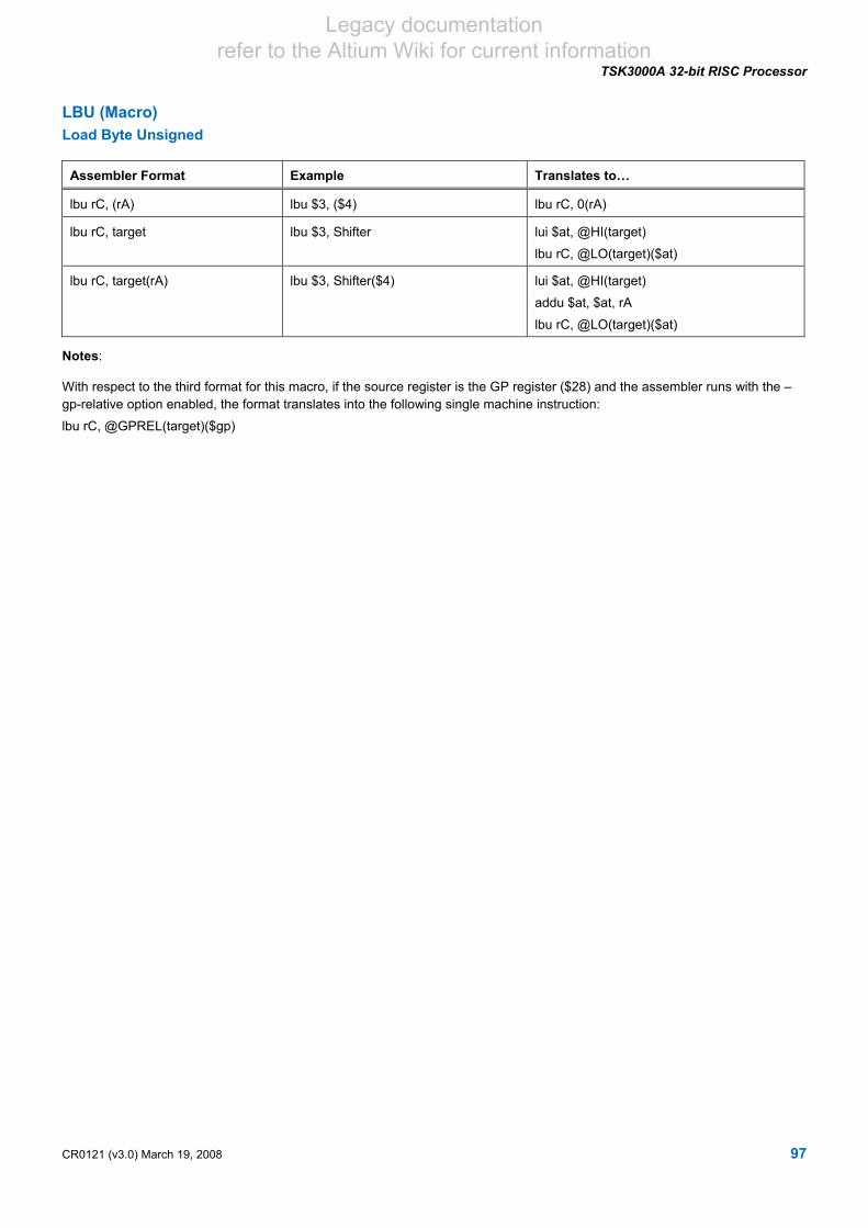
Legacy documentation refer to the Altium Wiki for current information
TSK3000A 32-bit RISC Processor
LBU (Macro) Load Byte Unsigned
Assembler Format Example Translates to…
lbu rC, (rA) lbu $3, ($4) lbu rC, 0(rA)
lbu rC, target lbu $3, Shifter lui $at, @HI(target)
lbu rC, @LO(target)($at)
lbu rC, target(rA) lbu $3, Shifter($4) lui $at, @HI(target)
addu $at, $at, rA
lbu rC, @LO(target)($at)
Notes:
With respect to the third format for this macro, if the source register is the GP register ($28) and the assembler runs with the –gp-relative option enabled, the format translates into the following single machine instruction:
lbu rC, @GPREL(target)($gp)
CR0121 (v3.0) March 19, 2008 97

Legacy documentation refer to the Altium Wiki for current information
TSK3000A 32-bit RISC Processor
LH Load Halfword
Assembler Format: lh rB, IMM16(rA)
Example: lh $3, 2($5)
Description: Generates a 32-bit effective address by sign-extending the 16-bit immediate value, IMM16, and adding it to the contents of GPR rA. It then sign-extends the halfword at the memory location pointed to by the effective address and loads the result into GPR rB.
Operation: rB ← SignExtend(Mem16[rA + SignExtend(IMM16)])
Instruction Type: I-Type
Instruction Fields: rA = Register index of operand A (base address)
rB = Register index of destination
IMM16 = 16-bit immediate data value
Encoding:
31 30 29 28 27 26 25 24 23 22 21 20 19 18 17 16 15 14 13 12 11 10 9 8 7 6 5 4 3 2 1 0
1 0 0 0 0 1 rA rB IMM16
Latency: 1
98 CR0121 (v3.0) March 19, 2008

Legacy documentation refer to the Altium Wiki for current information
TSK3000A 32-bit RISC Processor
LH (Macro) Load Halfword
Assembler Format Example Translates to…
lh rC, (rA) lh $3, ($4) lh rC, 0(rA)
lh rC, target lh $3, Shifter lui $at, @HI(target)
lh rC, @LO(target)($at)
lh rC, target(rA) lh $3, Shifter($4) lui $at, @HI(target)
addu $at, $at, rA
lh rC, @LO(target)($at)
Notes:
With respect to the third format for this macro, if the source register is the GP register ($28) and the assembler runs with the –gp-relative option enabled, the format translates into the following single machine instruction:
lh rC, @GPREL(target)($gp)
CR0121 (v3.0) March 19, 2008 99

Legacy documentation refer to the Altium Wiki for current information
TSK3000A 32-bit RISC Processor
LHU Load Halfword Unsigned
Assembler Format: lhu rB, IMM16(rA)
Example: lhu $3, 2($5)
Description: Generates a 32-bit effective address by sign-extending the 16-bit immediate value, IMM16, and adding it to the contents of GPR rA. It then zero-extends the halfword at the memory location pointed to by the effective address and loads the result into GPR rB.
Operation: rB ← ZeroExtend(Mem16[rA + SignExtend(IMM16)])
Instruction Type: I-Type
Instruction Fields: rA = Register index of operand A (base address)
rB = Register index of destination
IMM16 = 16-bit immediate data value
Encoding:
31 30 29 28 27 26 25 24 23 22 21 20 19 18 17 16 15 14 13 12 11 10 9 8 7 6 5 4 3 2 1 0
1 0 0 1 0 1 rA rB IMM16
Latency: 1
100 CR0121 (v3.0) March 19, 2008

Legacy documentation refer to the Altium Wiki for current information
TSK3000A 32-bit RISC Processor
LHU (Macro) Load Halfword Unsigned
Assembler Format Example Translates to…
lhu rC, (rA) lhu $3, ($4) lhu rC, 0(rA)
lhu rC, target lhu $3, Shifter lui $at, @HI(target)
lhu rC, @LO(target)($at)
lhu rC, target(rA) lhu $3, Shifter($4) lui $at, @HI(target)
addu $at, $at, rA
lhu rC, @LO(target)($at)
Notes:
With respect to the third format for this macro, if the source register is the GP register ($28) and the assembler runs with the –gp-relative option enabled, the format translates into the following single machine instruction:
lhu rC, @GPREL(target)($gp)
CR0121 (v3.0) March 19, 2008 101

Legacy documentation refer to the Altium Wiki for current information
TSK3000A 32-bit RISC Processor
LI (Macro) Load Immediate
Assembler Format Example Translates to…
li rC, IMM32 li $3, 0x12345678 see notes
Notes:
The expression should result in a 32-bit integer value in the range -231 to 232 – 1. There are four possible machine instruction representations of this macro instruction, depending on the value of the expression:
ori rC, $0, IMM32 if IMM32 is in the range 0 to 216 – 1 (i.e. from 0000_0000h to 0000_FFFFh)
addiu rC, $0, IMM32 if IMM32 is in the range -215 to -1 (i.e. from FFFF_8000h to FFFF_FFFFh)
lui rC, @MSH(IMM32) if IMM32 is a multiple of 216 (i.e. of the form xxxx_0000h)
lui $at, @MSH(IMM32)
ori rC, $at, @LSH(IMM32)
for all other values of IMM32
Relocatable expressions are not allowed.
102 CR0121 (v3.0) March 19, 2008

Legacy documentation refer to the Altium Wiki for current information
TSK3000A 32-bit RISC Processor
LUI Load Upper Immediate
Assembler Format: lui rB, IMM16
Example: lui $3, 0x0123456F + 2
Description: Left-shifts 16-bit immediate value, IMM16, by 16 bits, zero-fills the low-order 16 bits of the word, and puts the result in GPR rB.
Operation: rB ← ((IMM16 << 16) : 0000h)
Instruction Type: I-Type
Instruction Fields: rB = Register index of destination
IMM16 = 16-bit immediate data value
Encoding:
31 30 29 28 27 26 25 24 23 22 21 20 19 18 17 16 15 14 13 12 11 10 9 8 7 6 5 4 3 2 1 0
0 0 1 1 1 1 0 0 0 0 0 rB IMM16
Latency: 1
CR0121 (v3.0) March 19, 2008 103

Legacy documentation refer to the Altium Wiki for current information
TSK3000A 32-bit RISC Processor
LW Load Word
Assembler Format: lw rB, IMM16(rA)
Example: lw $3, 0($5)
Description: Generates a 32-bit effective address by sign-extending the 16-bit immediate value, IMM16, and adding it to the contents of GPR rA. It then loads the word at the memory location pointed to by the effective address into GPR rB.
Operation: rB ← Mem32[rA + SignExtend(IMM16)]
Instruction Type: I-Type
Instruction Fields: rA = Register index of operand A (base address)
rB = Register index of destination
IMM16 = 16-bit immediate data value
Encoding:
31 30 29 28 27 26 25 24 23 22 21 20 19 18 17 16 15 14 13 12 11 10 9 8 7 6 5 4 3 2 1 0
1 0 0 0 1 1 rA rB IMM16
Latency: 1
104 CR0121 (v3.0) March 19, 2008

Legacy documentation refer to the Altium Wiki for current information
TSK3000A 32-bit RISC Processor
LW (Macro) Load Word
Assembler Format Example Translates to…
lw rC, (rA) lw $3, ($4) lw rC, 0(rA)
lw rC, target lw $3, Shifter lui $at, @HI(target)
lw rC, @LO(target)($at)
lw rC, target(rA) lw $3, Shifter($4) lui $at, @HI(target)
addu $at, $at, rA
lw rC, @LO(target)($at)
Notes:
With respect to the third format for this macro, if the source register is the GP register ($28) and the assembler runs with the –gp-relative option enabled, the format translates into the following single machine instruction:
lw rC, @GPREL(target)($gp)
CR0121 (v3.0) March 19, 2008 105
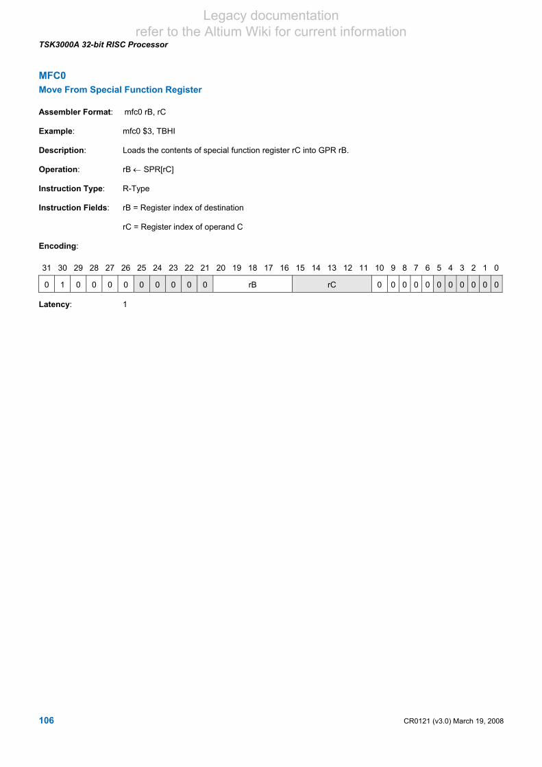
Legacy documentation refer to the Altium Wiki for current information
TSK3000A 32-bit RISC Processor
MFC0 Move From Special Function Register
Assembler Format: mfc0 rB, rC
Example: mfc0 $3, TBHI
Description: Loads the contents of special function register rC into GPR rB.
Operation: rB ← SPR[rC]
Instruction Type: R-Type
Instruction Fields: rB = Register index of destination
rC = Register index of operand C
Encoding:
31 30 29 28 27 26 25 24 23 22 21 20 19 18 17 16 15 14 13 12 11 10 9 8 7 6 5 4 3 2 1 0
0 1 0 0 0 0 0 0 0 0 0 rB rC 0 0 0 0 0 0 0 0 0 0 0
Latency: 1
106 CR0121 (v3.0) March 19, 2008

Legacy documentation refer to the Altium Wiki for current information
TSK3000A 32-bit RISC Processor
MFHI Move From HI
Assembler Format: mfhi rC
Example: mfhi $3
Description: Loads the contents of SFR HI into GPR rC.
Operation: rC ← HI
Instruction Type: R-Type
Instruction Fields: rC = Register index of destination
Encoding:
31 30 29 28 27 26 25 24 23 22 21 20 19 18 17 16 15 14 13 12 11 10 9 8 7 6 5 4 3 2 1 0
0 0 0 0 0 0 0 0 0 0 0 0 0 0 0 0 rC 0 0 0 0 0 0 1 0 0 0 0
Latency: 1
CR0121 (v3.0) March 19, 2008 107

Legacy documentation refer to the Altium Wiki for current information
TSK3000A 32-bit RISC Processor
MFLO Move From LO
Assembler Format: mflo rC
Example: mflo $3
Description: Loads the contents of SFR LO into GPR rC.
Operation: rC ← LO
Instruction Type: R-Type
Instruction Fields: rC = Register index of destination
Encoding:
31 30 29 28 27 26 25 24 23 22 21 20 19 18 17 16 15 14 13 12 11 10 9 8 7 6 5 4 3 2 1 0
0 0 0 0 0 0 0 0 0 0 0 0 0 0 0 0 rC 0 0 0 0 0 0 1 0 0 1 0
Latency: 1
108 CR0121 (v3.0) March 19, 2008

Legacy documentation refer to the Altium Wiki for current information
TSK3000A 32-bit RISC Processor
MTC0 Move To Special Function Register
Assembler Format: mtc0 rB, rC
Example: mtc0 $3, PIT
Description: Loads the contents of GPR rB into special function register rC.
Operation: SPR[Rc] ← rB
Instruction Type: R-Type
Instruction Fields: rB = Index of source GPR
rC = Index of destination SFR
Encoding:
31 30 29 28 27 26 25 24 23 22 21 20 19 18 17 16 15 14 13 12 11 10 9 8 7 6 5 4 3 2 1 0
0 1 0 0 0 0 0 0 1 0 0 rB rC 0 0 0 0 0 0 0 0 0 0 0
Latency: 1
CR0121 (v3.0) March 19, 2008 109
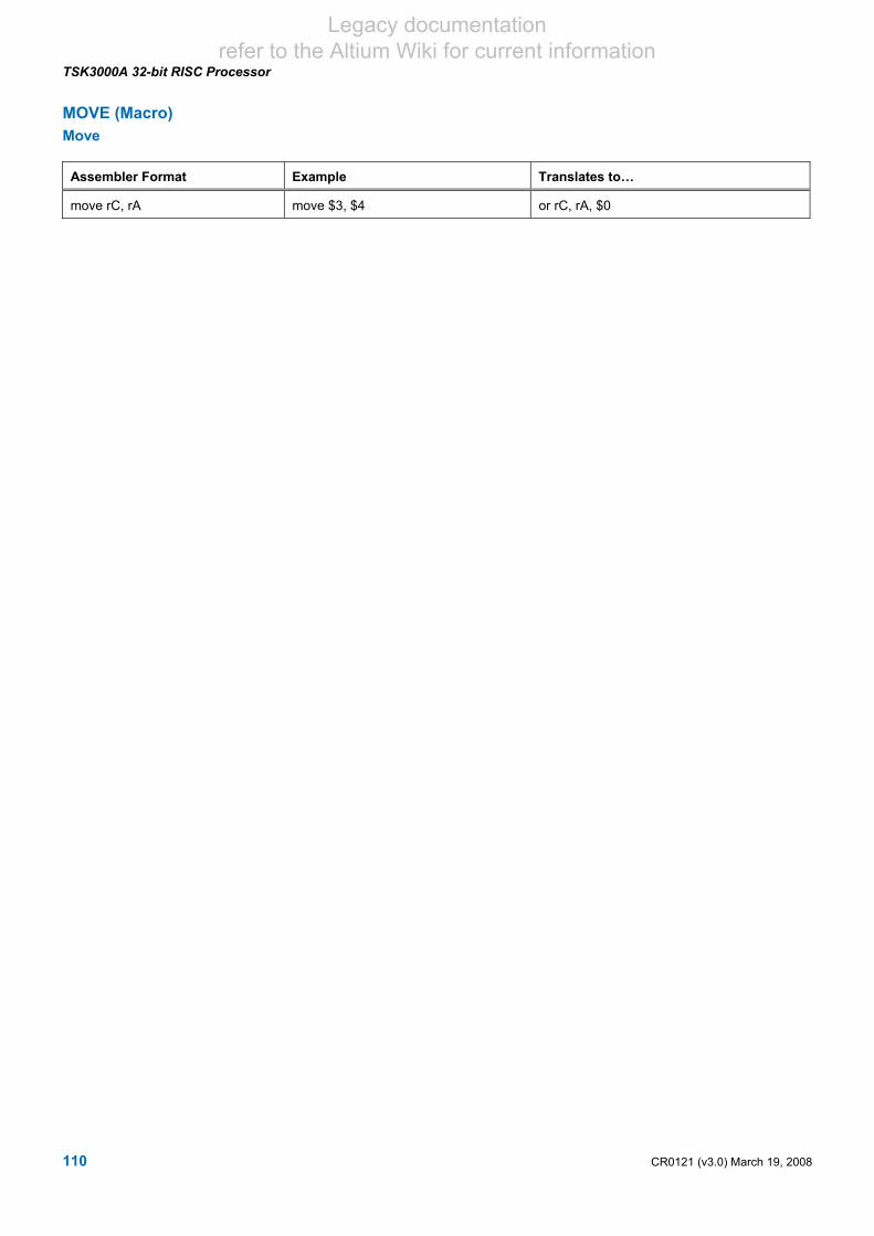
Legacy documentation refer to the Altium Wiki for current information
TSK3000A 32-bit RISC Processor
MOVE (Macro) Move
Assembler Format Example Translates to…
move rC, rA move $3, $4 or rC, rA, $0
110 CR0121 (v3.0) March 19, 2008

Legacy documentation refer to the Altium Wiki for current information
TSK3000A 32-bit RISC Processor
MTHI Move To HI
Assembler Format: mthi rA
Example: mthi $3
Description: Loads the contents of GPR rA into SFR HI.
Operation: HI ← rA
Instruction Type: R-Type
Instruction Fields: rA = Index of source GPR
Encoding:
31 30 29 28 27 26 25 24 23 22 21 20 19 18 17 16 15 14 13 12 11 10 9 8 7 6 5 4 3 2 1 0
0 0 0 0 0 0 rA 0 0 0 0 0 0 0 0 0 0 0 0 0 0 0 0 1 0 0 0 1
Latency: 1
CR0121 (v3.0) March 19, 2008 111

Legacy documentation refer to the Altium Wiki for current information
TSK3000A 32-bit RISC Processor
MTLO Move To LO
Assembler Format: mtlo rA
Example: mtlo $3
Description: Loads the contents of GPR rA into SFR LO.
Operation: LO ← rA
Instruction Type: R-Type
Instruction Fields: rA = Index of source GPR
Encoding:
31 30 29 28 27 26 25 24 23 22 21 20 19 18 17 16 15 14 13 12 11 10 9 8 7 6 5 4 3 2 1 0
0 0 0 0 0 0 rA 0 0 0 0 0 0 0 0 0 0 0 0 0 0 0 0 1 0 0 1 1
Latency: 1
112 CR0121 (v3.0) March 19, 2008

Legacy documentation refer to the Altium Wiki for current information
TSK3000A 32-bit RISC Processor
MULT Multiply Word
Assembler Format: mult rC, rA, rB
Example: mult $3, $4, $5
Description: Multiplies the contents of GPR rA by the contents of GPR rB, treating both operands as 32-bit two's complement values. The low-order word of the multiplication result is put in special register LO and also in GPR rC. The high-order word of the result is put in special register HI.
If rC is omitted in assembly language, $0 is used as the default value.
This instruction cannot raise an integer overflow exception.
Operation: HILO ← (Signed) rA * (Signed) rB
Instruction Type: R-Type
Instruction Fields: rA = Register index of operand A
rB = Register index of operand B
rC = Register index of destination
Encoding:
31 30 29 28 27 26 25 24 23 22 21 20 19 18 17 16 15 14 13 12 11 10 9 8 7 6 5 4 3 2 1 0
0 0 0 0 0 0 rA rB rC 0 0 0 0 0 0 1 1 0 0 0
Latency: 1
CR0121 (v3.0) March 19, 2008 113
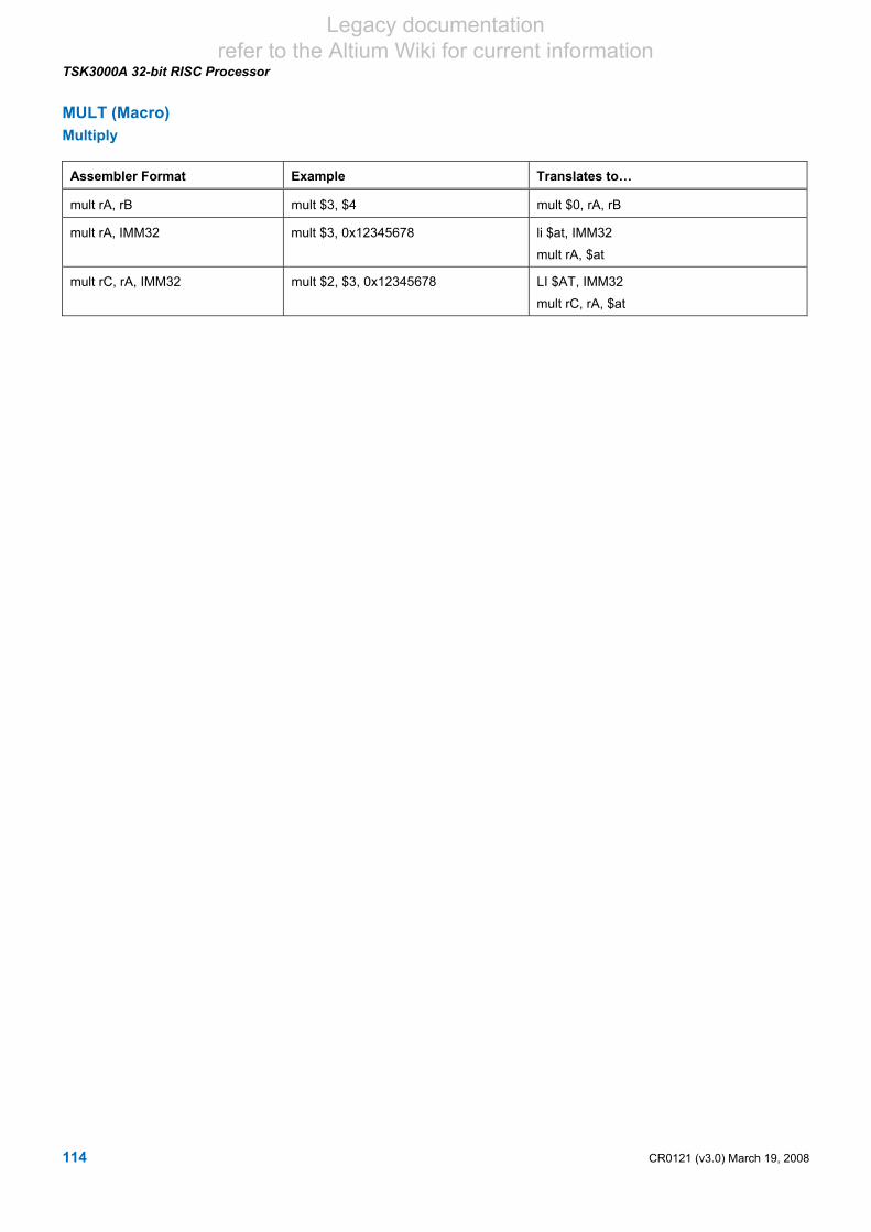
Legacy documentation refer to the Altium Wiki for current information
TSK3000A 32-bit RISC Processor
MULT (Macro) Multiply
Assembler Format Example Translates to…
mult rA, rB mult $3, $4 mult $0, rA, rB
mult rA, IMM32 mult $3, 0x12345678 li $at, IMM32
mult rA, $at
mult rC, rA, IMM32 mult $2, $3, 0x12345678 LI $AT, IMM32
mult rC, rA, $at
114 CR0121 (v3.0) March 19, 2008

Legacy documentation refer to the Altium Wiki for current information
TSK3000A 32-bit RISC Processor
MULTU Multiply Unsigned Word
Assembler Format: multu rC, rA, rB
Example: multu $3, $4, $5
Description: Multiplies the contents of GPR rA by the contents of GPR rB, treating both operands as 32-bit unsigned positive values. The low-order word of the multiplication result is put in special register LO and also in GPR rC. The high-order word of the result is put in special register HI.
If rC is omitted in assembly language, $0 is used as the default value.
This instruction cannot raise an integer overflow exception.
Operation: HILO ← (Unsigned) rA * (Unsigned) rB
Instruction Type: R-Type
Instruction Fields: rA = Register index of operand A
rB = Register index of operand B
rC = Register index of destination
Encoding:
31 30 29 28 27 26 25 24 23 22 21 20 19 18 17 16 15 14 13 12 11 10 9 8 7 6 5 4 3 2 1 0
0 0 0 0 0 0 rA rB rC 0 0 0 0 0 0 1 1 0 10
Latency: 1
CR0121 (v3.0) March 19, 2008 115

Legacy documentation refer to the Altium Wiki for current information
TSK3000A 32-bit RISC Processor
MULTU (Macro) Multiply Unsigned
Assembler Format Example Translates to…
multu rA, rB multu $3, $4 multu $0, rA, rB
multu rA, IMM32 multu $3, 0x12345678 li $at, IMM32
multu rA, $at
multu rC, rA, IMM32 multu $2, $3, 0x12345678 LI $AT, IMM32
multu rC, rA, $at
116 CR0121 (v3.0) March 19, 2008

Legacy documentation refer to the Altium Wiki for current information
TSK3000A 32-bit RISC Processor
NEG (Macro) Negate
Assembler Format Example Translates to…
neg rC, rA neg $3, $4 sub rC, $0, rA
neg rA neg $4 sub rA, $0, rA (with rC = rA)
CR0121 (v3.0) March 19, 2008 117

Legacy documentation refer to the Altium Wiki for current information
TSK3000A 32-bit RISC Processor
NEGU (Macro) Negate Unsigned
Assembler Format Example Translates to…
negu rC, rA negu $3, $4 subu rC, $0, rA
negu rA negu $4 subu rA, $0, rA (with rC = rA)
118 CR0121 (v3.0) March 19, 2008

Legacy documentation refer to the Altium Wiki for current information
TSK3000A 32-bit RISC Processor
NOP (Macro) No Operation
Assembler Format Example Translates to…
nop nop sll $0, $0, 0
CR0121 (v3.0) March 19, 2008 119

Legacy documentation refer to the Altium Wiki for current information
TSK3000A 32-bit RISC Processor
NOR Bitwise Logical NOR
Assembler Format: nor rC, rA, rB
Example: nor $3, $4, $5
Description: Bitwise logically NORs the contents of GPR rA with the contents of GPR rB, and loads the result in GPR rC.
Operation: rC ← rA NOR rB
Instruction Type: R-Type
Instruction Fields: rA = Register index of operand A
rB = Register index of operand B
rC = Register index of destination
Encoding:
31 30 29 28 27 26 25 24 23 22 21 20 19 18 17 16 15 14 13 12 11 10 9 8 7 6 5 4 3 2 1 0
0 0 0 0 0 0 rA rB rC 0 0 0 0 0 1 0 0 1 1 1
Latency: 1
120 CR0121 (v3.0) March 19, 2008

Legacy documentation refer to the Altium Wiki for current information
TSK3000A 32-bit RISC Processor
NOR (Macro) Bitwise Logical NOR
Assembler Format Example Translates to…
nor rC, rB nor $3, $4 nor rC, rC, rB (with rA = rC)
nor rC, rA, IMM32 nor $3, $4, 0x12345678
nor rC, IMM32 nor $3, 0x12345678
li $at, IMM32
nor rC, rA, $at
CR0121 (v3.0) March 19, 2008 121

Legacy documentation refer to the Altium Wiki for current information
TSK3000A 32-bit RISC Processor
NOT (Macro) Bitwise Logical NOT
Assembler Format Example Translates to…
not rC, rA not $3, $4 nor rC, rA, $0
not rA not $4 nor rA, rA, $0 (with rC = rA)
122 CR0121 (v3.0) March 19, 2008

Legacy documentation refer to the Altium Wiki for current information
TSK3000A 32-bit RISC Processor
OR Bitwise Logical OR
Assembler Format: or rC, rA, rB
Example: or $3, $4, $5
Description: Bitwise logically ORs the contents of GPR rA with the contents of GPR rB, and loads the result in GPR rC.
Operation: rC ← rA OR rB
Instruction Type: R-Type
Instruction Fields: rA = Register index of operand A
rB = Register index of operand B
rC = Register index of destination
Encoding:
31 30 29 28 27 26 25 24 23 22 21 20 19 18 17 16 15 14 13 12 11 10 9 8 7 6 5 4 3 2 1 0
0 0 0 0 0 0 rA rB rC 0 0 0 0 0 1 0 0 1 0 1
Latency: 1
CR0121 (v3.0) March 19, 2008 123
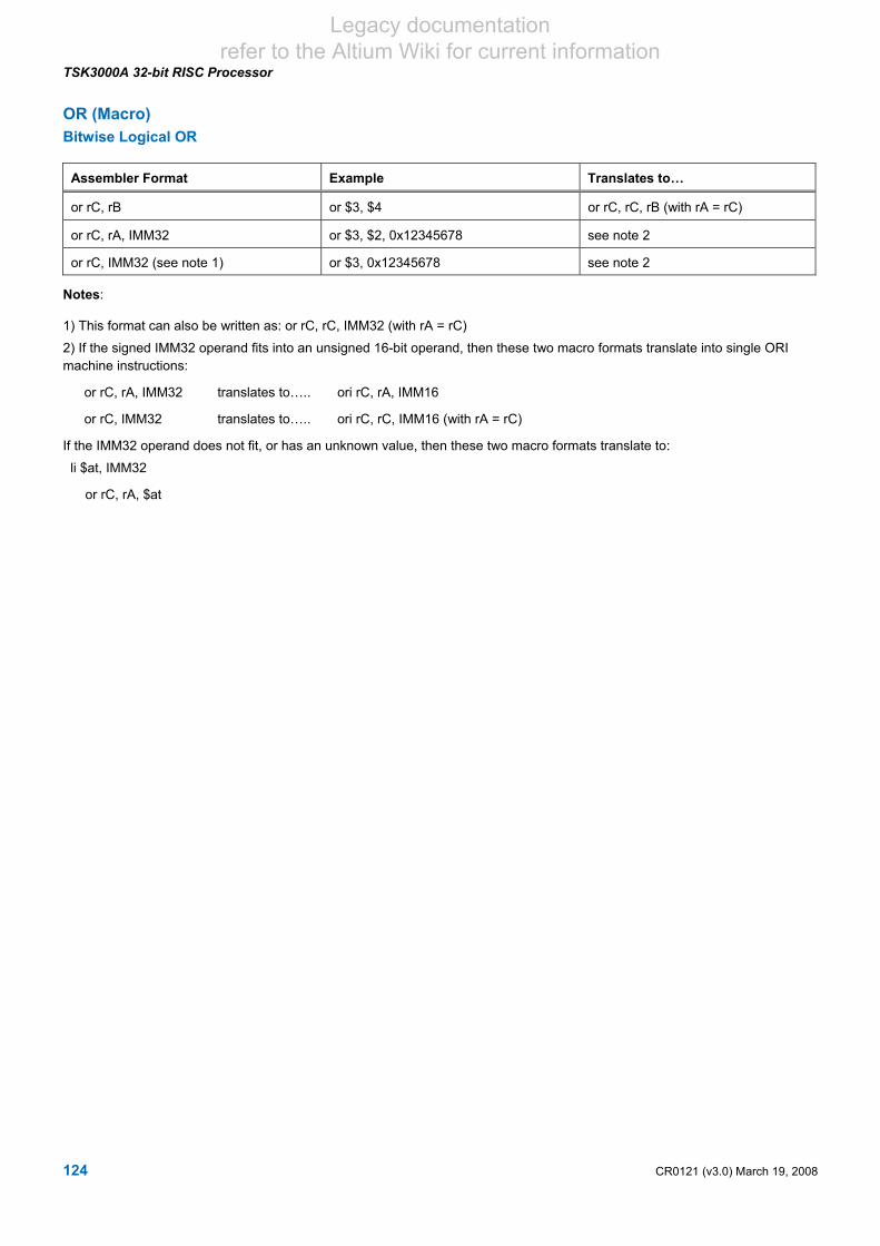
Legacy documentation refer to the Altium Wiki for current information
TSK3000A 32-bit RISC Processor
OR (Macro) Bitwise Logical OR
Assembler Format Example Translates to…
or rC, rB or $3, $4 or rC, rC, rB (with rA = rC)
or rC, rA, IMM32 or $3, $2, 0x12345678 see note 2
or rC, IMM32 (see note 1) or $3, 0x12345678 see note 2
Notes:
1) This format can also be written as: or rC, rC, IMM32 (with rA = rC)
2) If the signed IMM32 operand fits into an unsigned 16-bit operand, then these two macro formats translate into single ORI machine instructions:
or rC, rA, IMM32 translates to….. ori rC, rA, IMM16
or rC, IMM32 translates to….. ori rC, rC, IMM16 (with rA = rC)
If the IMM32 operand does not fit, or has an unknown value, then these two macro formats translate to:
li $at, IMM32
or rC, rA, $at
124 CR0121 (v3.0) March 19, 2008

Legacy documentation refer to the Altium Wiki for current information
TSK3000A 32-bit RISC Processor
ORI Bitwise Logical OR Immediate
Assembler Format: ori rB, rA, IMM16
Example: ori $3, $4, 0x1234
Description: Zero-extends the 16-bit immediate value, IMM16, bitwise logically ORs the result with the contents of GPR rA, and loads the result in GPR rB.
Operation: rB ← rA OR ZeroExtend(IMM16)
Instruction Type: I-Type
Instruction Fields: rA = Register index of operand A
rB = Register index of destination
IMM16 = 16-bit immediate data value
Encoding:
31 30 29 28 27 26 25 24 23 22 21 20 19 18 17 16 15 14 13 12 11 10 9 8 7 6 5 4 3 2 1 0
0 0 1 1 0 1 rA rB IMM16
Latency: 1
CR0121 (v3.0) March 19, 2008 125

Legacy documentation refer to the Altium Wiki for current information
TSK3000A 32-bit RISC Processor
ORI (Macro) Bitwise Logical OR Immediate
Assembler Format Example Translates to…
ori rC, IMM16 ori $3, oxFFFF ori rC, rC, IMM16 (where rA = rC)
126 CR0121 (v3.0) March 19, 2008
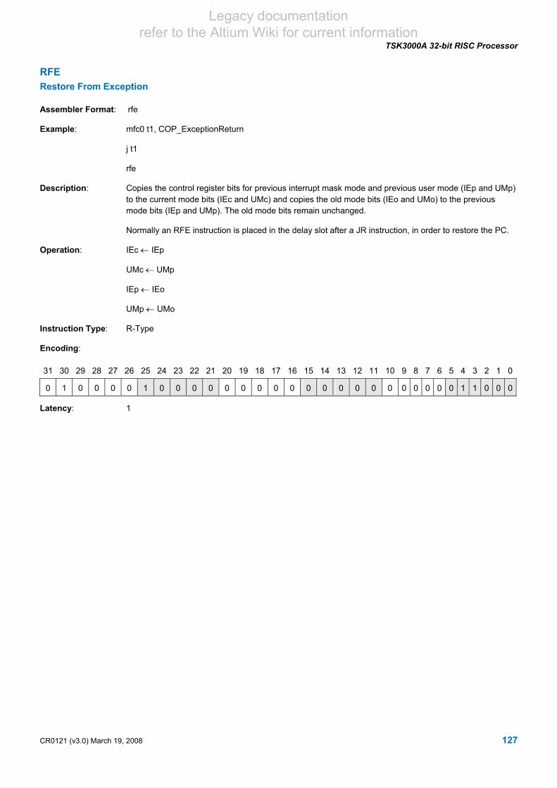
Legacy documentation refer to the Altium Wiki for current information
TSK3000A 32-bit RISC Processor
RFE Restore From Exception
Assembler Format: rfe
Example: mfc0 t1, COP_ExceptionReturn
j t1
rfe
Description: Copies the control register bits for previous interrupt mask mode and previous user mode (IEp and UMp) to the current mode bits (IEc and UMc) and copies the old mode bits (IEo and UMo) to the previous mode bits (IEp and UMp). The old mode bits remain unchanged.
Normally an RFE instruction is placed in the delay slot after a JR instruction, in order to restore the PC.
Operation: IEc ← IEp
UMc ← UMp
IEp ← IEo
UMp ← UMo
Instruction Type: R-Type
Encoding:
31 30 29 28 27 26 25 24 23 22 21 20 19 18 17 16 15 14 13 12 11 10 9 8 7 6 5 4 3 2 1 0
0 1 0 0 0 0 1 0 0 0 0 0 0 0 0 0 0 0 0 0 0 0 0 0 0 0 0 1 1 0 0 0
Latency: 1
CR0121 (v3.0) March 19, 2008 127

Legacy documentation refer to the Altium Wiki for current information
TSK3000A 32-bit RISC Processor
ROL (Macro) Rotate Left
Assembler Format Example Translates to…
rol rC, rA, IMM5 rol $3, $4, 16 srl $at, rA, 32 – IMM5
sll rC, rA, IMM5
or rC, rC, $at
rol rC, rA, rB rol $3, $4, $5 subu $at, $0, rB
srlv $at, rA, $at
sllv rC, rA, rB
or rC, rC, $at
rol rC, IMM5 rol $3, 16 srl $at, rC, 32 – IMM5
sll rC, rC, IMM5
or rC, rC, $at
rol rC, rB rol $3, $5 subu $at, $0, rB
srlv $at, rC, $at
sllv rC, rC, rB
or rC, rC, $at
128 CR0121 (v3.0) March 19, 2008

Legacy documentation refer to the Altium Wiki for current information
TSK3000A 32-bit RISC Processor
ROR (Macro) Rotate Right
Assembler Format Example Translates to…
ror rC, rA, IMM5 ror $3, $4, 16 sll $at, rA, 32 – IMM5
srl rC, rA, IMM5
or rC, rC, $at
ror rC, rA, rB ror $3, $4, $5 subu $at, $0, rB
sllv $at, rA, $at
srlv rC, rA, rB
or rC, rC, $at
ror rC, IMM5 ror $3, 16 sll $at, rC, 32 – IMM5
srl rC, rC, IMM5
or rC, rC, $at
ror rC, rB ror $3, $5 subu $at, $0, rB
sllv $at, rC, $at
srlv rC, rC, rB
or rC, rC, $at
CR0121 (v3.0) March 19, 2008 129

Legacy documentation refer to the Altium Wiki for current information
TSK3000A 32-bit RISC Processor
SB Store Byte
Assembler Format: sb rB, IMM16(rA)
Example: sb $3, 2($5)
Description: Generates a 32-bit effective address by sign-extending the 16-bit immediate value, IMM16, and adding it to the contents of GPR rA. It then stores the least significant byte of register rB at the resulting effective address.
Operation: Mem8[rA + SignExtend(IMM16)] ← rB7..0
Instruction Type: I-Type
Instruction Fields: rA = Register index of operand A
rB = Register index of operand B
IMM16 = 16-bit immediate data value
Encoding:
31 30 29 28 27 26 25 24 23 22 21 20 19 18 17 16 15 14 13 12 11 10 9 8 7 6 5 4 3 2 1 0
1 0 1 0 0 0 rA rB IMM16
Latency: 1
130 CR0121 (v3.0) March 19, 2008

Legacy documentation refer to the Altium Wiki for current information
TSK3000A 32-bit RISC Processor
SB (Macro) Store Byte
Assembler Format Example Translates to…
sb rC, (rA) sb $3, ($4) sb rC, 0(rA)
sb rC, target sb $3, Shifter lui $at, @HI(target)
sb rC, @LO(target)($at)
sb rC, target(rA) sb $3, Shifter($4) lui $at, @HI(target)
addu $at, $at, rA
sb rC, @LO(target)($at)
Notes:
With respect to the third format for this macro, if the source register is the GP register ($28) and the assembler runs with the –gp-relative option enabled, the format translates into the following single machine instruction:
sb rC, @GPREL(target)($gp)
CR0121 (v3.0) March 19, 2008 131

Legacy documentation refer to the Altium Wiki for current information
TSK3000A 32-bit RISC Processor
SEQ (Macro) Set On Equal To
Assembler Format Example Translates to…
seq rC, rA, rB seq $3, $4, $5 xor rC, rA, rB
sltiu rC, rC, 1
seq rC, rA, IMM32 seq $3, $4, 0x12345678 li $at, IMM32
xor rC, rA, $AT
sltiu rC, rC, 1
Notes:
If IMM32 is in the range 0 to 216 – 1 (i.e. from 0000_0000h to 0000_FFFFh) then the second macro format translates to:
xori rC, rA, IMM32
sltiu rC, rC, 1
132 CR0121 (v3.0) March 19, 2008

Legacy documentation refer to the Altium Wiki for current information
TSK3000A 32-bit RISC Processor
SGE (Macro) Set On Greater Than Or Equal To
Assembler Format Example Translates to…
sge rC, rA, rB sge $3, $4, $5 slt rC, rA, rB
xori rC, rC, 1
sge rC, rA, IMM32 sge $3, $4, 0x12345678 li $at, IMM32
slt rC, rA, $at
xori rC, rC, 1
Notes:
If IMM32 is in the range -215 to 215 – 1 (i.e. from 0000_0000h to 0000_7FFFh or from FFFF_8000h to FFFF_FFFFh) then the second macro format translates to:
slti rC, rA, IMM32
xori rC, rC, 1
CR0121 (v3.0) March 19, 2008 133

Legacy documentation refer to the Altium Wiki for current information
TSK3000A 32-bit RISC Processor
SGEU (Macro) Set On Greater Than Or Equal To Unsigned
Assembler Format Example Translates to…
sgeu rC, rA, rB sgeu $3, $4, $5 sltu rC, rA, rB
xori rC, rC, 1
sgeu rC, rA, IMM32 sgeu $3, $4, 0x12345678 li $at, IMM32
sltu rC, rA, $at
xori rC, rC, 1
Notes:
If IMM32 is in the range -215 to 215 – 1 (i.e. from 0000_0000h to 0000_7FFFh or from FFFF_8000h to FFFF_FFFFh) then the second macro format translates to:
sltiu rC, rA, IMM32
xori rC, rC, 1
134 CR0121 (v3.0) March 19, 2008

Legacy documentation refer to the Altium Wiki for current information
TSK3000A 32-bit RISC Processor
SGT (Macro) Set On Greater Than
Assembler Format Example Translates to…
sgt rC, rA, rB sgt $3, $4, $5 slt rC, rB, rA
sgt rC, rA, IMM32 sgt $3, $4, 0x12345678 li $at, IMM32
slt rC, $at, rA
CR0121 (v3.0) March 19, 2008 135

Legacy documentation refer to the Altium Wiki for current information
TSK3000A 32-bit RISC Processor
SGTU (Macro) Set On Greater Than Unsigned
Assembler Format Example Translates to…
sgtu rC, rA, rB sgtu $3, $4, $5 sltu rC, rB, rA
sgtu rC, rA, IMM32 sgtu $3, $4, 0x12345678 li $at, IMM32
sltu rC, $at, rA
136 CR0121 (v3.0) March 19, 2008

Legacy documentation refer to the Altium Wiki for current information
TSK3000A 32-bit RISC Processor
SH Store Halfword
Assembler Format: sh rB, IMM16(rA)
Example: sh $3, 2($5)
Description: Generates an unsigned 32-bit effective address by sign-extending the 16-bit immediate value, IMM16, and adding it to the contents of GPR rA. It then stores the least significant halfword of register rB at the resulting effective address.
Operation: Mem16[rA + SignExtend(IMM16)] ← rB15..0
Instruction Type: I-Type
Instruction Fields: rA = Register index of operand A
rB = Register index of operand B
IMM16 = 16-bit immediate data value
Encoding:
31 30 29 28 27 26 25 24 23 22 21 20 19 18 17 16 15 14 13 12 11 10 9 8 7 6 5 4 3 2 1 0
1 0 1 0 0 1 rA rB IMM16
Latency: 1
CR0121 (v3.0) March 19, 2008 137

Legacy documentation refer to the Altium Wiki for current information
TSK3000A 32-bit RISC Processor
SH (Macro) Store Halfword
Assembler Format Example Translates to…
sh rC, (rA) sh $3, ($4) sh rC, 0(rA)
sh rC, target sh $3, Shifter lui $at, @HI(target)
sh rC, @LO(target)($at)
sh rC, target(rA) sh $3, Shifter($4) lui $at, @HI(target)
addu $at, $at, rA
sh rC, @LO(target)($at)
Notes:
With respect to the third format for this macro, if the source register is the GP register ($28) and the assembler runs with the –gp-relative option enabled, the format translates into the following single machine instruction:
sh rC, @GPREL(target)($gp)
138 CR0121 (v3.0) March 19, 2008

Legacy documentation refer to the Altium Wiki for current information
TSK3000A 32-bit RISC Processor
SLA (Macro) Shift Left Arithmetic
Assembler Format Example Translates to…
sla rC, rA, IMM5 sla $3, $4, 4 sll rC, rA, IMM5
sla rC, rA, rB sla $3, $4, $5 sllv rC, rA, rB
sla rC, IMM5 sla $3, 4 sll rC, rC, IMM5 (where rA = rC)
sla rC, rB sla $3, $5 sllv rC, rC, rB (where rA = rC)
Notes:
SLA is identical to SLL and can be used wherever SLL is used.
CR0121 (v3.0) March 19, 2008 139

Legacy documentation refer to the Altium Wiki for current information
TSK3000A 32-bit RISC Processor
SLAV (Macro) Shift Left Arithmetic Variable
Assembler Format Example Translates to…
slav rC, rA, rB slav $3, $4, $5 sllv rC, rA, rB
slav rC, rB slav $3, $5 sllv rC, rC, rB (where rA = rC)
Notes:
SLAV is identical to SLLV and can be used wherever SLLV is used.
140 CR0121 (v3.0) March 19, 2008

Legacy documentation refer to the Altium Wiki for current information
TSK3000A 32-bit RISC Processor
SLE (Macro) Set On Less Than Or Equal To
Assembler Format Example Translates to…
sle rC, rA, rB sle $3, $4, $5 slt rC, rB, rA
xori rC, rC, 1
sle rC, rA, IMM32 sle $3, $4, 0x12345678 li $at, IMM32
slt rC, $at, rA
xori rC, rC, 1
CR0121 (v3.0) March 19, 2008 141

Legacy documentation refer to the Altium Wiki for current information
TSK3000A 32-bit RISC Processor
SLEU (Macro) Set On Less Than Or Equal To Unsigned
Assembler Format Example Translates to…
sleu rC, rA, rB sleu $3, $4, $5 sltu rC, rB, rA
xori rC, rC, 1
sleu rC, rA, IMM32 sleu $3, $4, 0x12345678 li $at, IMM32
sltu rC, $at, rA
xori rC, rC, 1
142 CR0121 (v3.0) March 19, 2008

Legacy documentation refer to the Altium Wiki for current information
TSK3000A 32-bit RISC Processor
SLL Shift Left Logical
Assembler Format: sll rC, rB, IMM5
Example: sll $3, $4, 4
Description: Left-shifts the contents of GPR rB by the number of bits specified by the immediate value, IMM5. Then zero-fills the low-order bits and puts the result in GPR rC.
Operation: rC ← rB << IMM5
Instruction Type: R-Type
Instruction Fields: rB = Register index of operand B
rC = Register index of destination
IMM5 = 5-bit immediate data value (shift amount)
Encoding:
31 30 29 28 27 26 25 24 23 22 21 20 19 18 17 16 15 14 13 12 11 10 9 8 7 6 5 4 3 2 1 0
0 0 0 0 0 0 0 0 0 0 0 rB rC IMM5 0 0 0 0 0 0
Latency: 1
Notes:
SLA is identical to SLL and can be used wherever SLL is used.
CR0121 (v3.0) March 19, 2008 143

Legacy documentation refer to the Altium Wiki for current information
TSK3000A 32-bit RISC Processor
SLL (Macro) Shift Left Logical
Assembler Format Example Translates to…
sll rC, rA, rB sll $3, $4, $5 sllv rC, rA, rB
sll rC, IMM5 sll $3, 4 sll rC, rC, IMM5 (where rA = rC)
sll rC, rB sll $3, $5 sllv rC, rC, rB (where rA = rC)
Notes:
SLA is identical to SLL and can be used wherever SLL is used.
144 CR0121 (v3.0) March 19, 2008

Legacy documentation refer to the Altium Wiki for current information
TSK3000A 32-bit RISC Processor
SLLV Shift Left Logical Variable
Assembler Format: sllv rC, rB, rA
Example: sllv $3, $4, $5
Description: Left-shifts the contents of GPR rB (by the number of bits designated by the low-order five bits of GPR rA), zero-fills the low-order bits and puts the 32-bit result in GPR rC.
Operation: rC ← rB << rA4..0
Instruction Type: R-Type
Instruction Fields: rA = Register index of operand A (shift amount)
rB = Register index of operand B
rC = Register index of destination
Encoding:
31 30 29 28 27 26 25 24 23 22 21 20 19 18 17 16 15 14 13 12 11 10 9 8 7 6 5 4 3 2 1 0
0 0 0 0 0 0 rA rB rC 0 0 0 0 0 0 0 0 1 0 0
Latency: 1
Notes:
SLAV is identical to SLLV and can be used wherever SLLV is used.
CR0121 (v3.0) March 19, 2008 145

Legacy documentation refer to the Altium Wiki for current information
TSK3000A 32-bit RISC Processor
SLLV (Macro) Shift Left Logical Variable
Assembler Format Example Translates to…
sllv rC, rB sllv $3, $4 sllv rC, rC, rB (where rA = rC)
Notes:
SLAV is identical to SLLV and can be used wherever SLLV is used.
146 CR0121 (v3.0) March 19, 2008

Legacy documentation refer to the Altium Wiki for current information
TSK3000A 32-bit RISC Processor
SLT Set On Less Than
Assembler Format: slt rC, rA, rB
Example: slt $3, $4, $5
Description: Compares the contents of GPRs rB and rA as 32-bit signed integers. If rA is less than rB, a ‘1’ is placed into GPR rC, otherwise GPR rC is loaded with ‘0’.
Operation: If rA < rB Then
rC ← 1
Else
rC ← 0
Instruction Type: R-Type
Instruction Fields: rA = Register index of operand A
rB = Register index of operand B
rC = Register index of destination
Encoding:
31 30 29 28 27 26 25 24 23 22 21 20 19 18 17 16 15 14 13 12 11 10 9 8 7 6 5 4 3 2 1 0
0 0 0 0 0 0 rA rB rC 0 0 0 0 0 1 0 1 0 1 0
Latency: 1
CR0121 (v3.0) March 19, 2008 147

Legacy documentation refer to the Altium Wiki for current information
TSK3000A 32-bit RISC Processor
SLT (Macro) Set On Less Than
Assembler Format Example Translates to…
slt rC, rB slt $3, $4 slt rC, rC, rB (with rA = rC)
slt rC, rA, IMM32 slt $3, $2, 0x12345678 see note 2
slt rC, IMM32 (see note 1) slt $3, 0x12345678 see note 2
Notes:
1) This format can also be written as: slt rC, rC, IMM32 (with rA = rC)
2) If the signed IMM32 operand fits into a signed 16-bit operand, then these two macro formats translate into single SLTI machine instructions:
slt rC, rA, IMM32 translates to….. slti rC, rA, IMM16
slt rC, IMM32 translates to….. slti rC, rC, IMM16 (with rA = rC)
If the IMM32 operand does not fit, or has an unknown value, then these two macro formats translate to:
li $at, IMM32
slt rC, rA, $at
148 CR0121 (v3.0) March 19, 2008

Legacy documentation refer to the Altium Wiki for current information
TSK3000A 32-bit RISC Processor
SLTI Set On Less Than Immediate
Assembler Format: slti rB, rA, IMM16
Example: slti $3, $4, 0x8764
Description: Sign-extends the 16-bit immediate value, IMM16 and compares the result with the contents of GPR rA, treating both values as 32-bit signed integers. If rA is less than the sign extended IMM16 value, a ‘1’ is placed into GPR rB, otherwise GPR rB is loaded with ‘0’.
Operation: If rA < SignExtend(IMM16) Then
rB ← 1
Else
rB ← 0
Instruction Type: R-Type
Instruction Fields: rA = Register index of operand A
rB = Register index of destination
IMM16 = 16-bit immediate data value
Encoding:
31 30 29 28 27 26 25 24 23 22 21 20 19 18 17 16 15 14 13 12 11 10 9 8 7 6 5 4 3 2 1 0
0 0 1 0 1 0 rA rB IMM16
Latency: 1
CR0121 (v3.0) March 19, 2008 149

Legacy documentation refer to the Altium Wiki for current information
TSK3000A 32-bit RISC Processor
SLTI (Macro) Set On Less Than Immediate
Assembler Format Example Translates to…
slti rC, IMM16 slti $3, oxFFFF slti rC, rC, IMM16 (where rA = rC)
150 CR0121 (v3.0) March 19, 2008

Legacy documentation refer to the Altium Wiki for current information
TSK3000A 32-bit RISC Processor
SLTIU Set On Less Than Immediate Unsigned
Assembler Format: sltiu rB, rA, IMM16
Example: sltiu $3, $4, 0x1234
Description: Sign-extends the 16-bit immediate value, IMM16 and compares the result with the contents of GPR rA, treating both values as 32-bit unsigned integers. If rA is less than the sign extended IMM16 value, a ‘1’ is placed into GPR rB, otherwise GPR rB is loaded with ‘0’.
Operation: If (Unsigned)rA < (Unsigned)SignExtend(IMM16) Then
rB ← 1
Else
rB ← 0
Instruction Type: I-Type
Instruction Fields: rA = Register index of operand A
rB = Register index of destination
IMM16 = 16-bit immediate data value
Encoding:
31 30 29 28 27 26 25 24 23 22 21 20 19 18 17 16 15 14 13 12 11 10 9 8 7 6 5 4 3 2 1 0
0 0 1 0 1 1 rA rB IMM16
Latency: 1
CR0121 (v3.0) March 19, 2008 151

Legacy documentation refer to the Altium Wiki for current information
TSK3000A 32-bit RISC Processor
SLTIU (Macro) Set On Less Than Immediate Unsigned
Assembler Format Example Translates to…
sltiu rC, IMM16 sltiu $3, oxFFFF sltiu rC, rC, IMM16 (where rA = rC)
152 CR0121 (v3.0) March 19, 2008

Legacy documentation refer to the Altium Wiki for current information
TSK3000A 32-bit RISC Processor
SLTU Set On Less Than Unsigned
Assembler Format: sltu rC, rA, rB
Example: sltu $3, $4, $5
Description: Compares the contents of GPRs rB and rA as 32-bit unsigned integers. If rA is less than rB, a ‘1’ is placed into GPR rC, otherwise GPR rC is loaded with ‘0’.
Operation: If (Unsigned)rA < (Unsigned)rB Then
rC ← 1
Else
rC ← 0
Instruction Type: R-Type
Instruction Fields: rA = Register index of operand A
rB = Register index of operand B
rC = Register index of destination
Encoding:
31 30 29 28 27 26 25 24 23 22 21 20 19 18 17 16 15 14 13 12 11 10 9 8 7 6 5 4 3 2 1 0
0 0 0 0 0 0 rA rB rC 0 0 0 0 0 1 0 1 0 1 1
Latency: 1
CR0121 (v3.0) March 19, 2008 153

Legacy documentation refer to the Altium Wiki for current information
TSK3000A 32-bit RISC Processor
SLTU (Macro) Set On Less Than Unsigned
Assembler Format Example Translates to…
sltu rC, rB sltu $3, $4 sltu rC, rC, rB (with rA = rC)
sltu rC, rA, IMM32 sltu $3, $2, 0x12345678 see note 2
sltu rC, IMM32 (see note 1) sltu $3, 0x12345678 see note 2
Notes:
1) This format can also be written as: sltu rC, rC, IMM32 (with rA = rC)
2) If the signed IMM32 operand fits into a signed 16-bit operand, then these two macro formats translate into single SLTIU machine instructions:
sltu rC, rA, IMM32 translates to….. sltiu rC, rA, IMM16
sltu rC, IMM32 translates to….. sltiu rC, rC, IMM16 (with rA = rC)
If the IMM32 operand does not fit, or has an unknown value, then these two macro formats translate to:
li $at, IMM32
sltu rC, rA, $a
154 CR0121 (v3.0) March 19, 2008

Legacy documentation refer to the Altium Wiki for current information
TSK3000A 32-bit RISC Processor
SNE (Macro) Set On Not Equal To
Assembler Format Example Translates to…
sne rC, rA, rB sne $3, $4, $5 xor rC, rA, rB
sltu rC, $0, rC
sne rC, rA, IMM32 sne $3, $4, 0x12345678 li $at, IMM32
xor rC, rA, rB
sltu rC, $0, rC
Notes:
If IMM32 is in the range 0 to 216 – 1 (i.e. from 0000_0000h to 0000_FFFFh) then the second macro format translates to:
xori rC, rA, IMM32
sltu rC, $0, rC
CR0121 (v3.0) March 19, 2008 155

Legacy documentation refer to the Altium Wiki for current information
TSK3000A 32-bit RISC Processor
SRA Shift Right Arithmetic
Assembler Format: sra rC, rB, IMM5
Example: sra $3, $4, 4
Description: Right-shifts the contents of GPR rB by the number of bits specified by the immediate value, IMM5. The high-order (IMM5) bits become sign-extended and the resulting word is put in GPR rC.
Operation: rC ← rB >> IMM5
Instruction Type: R-Type
Instruction Fields: rB = Register index of operand B
rC = Register index of destination
IMM5 = 5-bit immediate data value (shift amount)
Encoding:
31 30 29 28 27 26 25 24 23 22 21 20 19 18 17 16 15 14 13 12 11 10 9 8 7 6 5 4 3 2 1 0
0 0 0 0 0 0 0 0 0 0 0 rB rC IMM5 0 0 0 0 1 1
Latency: 1
156 CR0121 (v3.0) March 19, 2008

Legacy documentation refer to the Altium Wiki for current information
TSK3000A 32-bit RISC Processor
SRA (Macro) Shift Right Arithmetic
Assembler Format Example Translates to…
sra rC, rA, rB sra $3, $4, $5 srav rC, rA, rB
sra rC, IMM5 sra $3, 4 sra rC, rC, IMM5 (where rA = rC)
sra rC, rB sra $3, $5 srav rC, rC, rB (where rA = rC)
CR0121 (v3.0) March 19, 2008 157
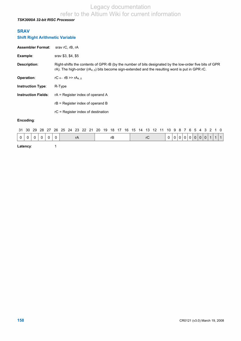
Legacy documentation refer to the Altium Wiki for current information
TSK3000A 32-bit RISC Processor
SRAV Shift Right Arithmetic Variable
Assembler Format: srav rC, rB, rA
Example: srav $3, $4, $5
Description: Right-shifts the contents of GPR rB (by the number of bits designated by the low-order five bits of GPR rA). The high-order (rA4..0) bits become sign-extended and the resulting word is put in GPR rC.
Operation: rC ← rB >> rA4..0
Instruction Type: R-Type
Instruction Fields: rA = Register index of operand A
rB = Register index of operand B
rC = Register index of destination
Encoding:
31 30 29 28 27 26 25 24 23 22 21 20 19 18 17 16 15 14 13 12 11 10 9 8 7 6 5 4 3 2 1 0
0 0 0 0 0 0 rA rB rC 0 0 0 0 0 0 0 0 1 1 1
Latency: 1
158 CR0121 (v3.0) March 19, 2008

Legacy documentation refer to the Altium Wiki for current information
TSK3000A 32-bit RISC Processor
SRAV (Macro) Shift Right Arithmetic Variable
Assembler Format Example Translates to…
srav rC, rB srav $3, $4 srav rC, rC, rB (where rA = rC)
CR0121 (v3.0) March 19, 2008 159

Legacy documentation refer to the Altium Wiki for current information
TSK3000A 32-bit RISC Processor
SRL Shift Right Logical
Assembler Format: srl rC, rB, IMM5
Example: srl $3, $4, 4
Description: Right-shifts the contents of GPR rB by the number of bits specified by the immediate value, IMM5. Then zero-fills the high-order (IMM5) bits and puts the result in GPR rC.
Operation: rC ← rB >> IMM5
Instruction Type: R-Type
Instruction Fields: rB = Register index of operand B
rC = Register index of destination
IMM5 = 5-bit immediate data value (shift amount)
Encoding:
31 30 29 28 27 26 25 24 23 22 21 20 19 18 17 16 15 14 13 12 11 10 9 8 7 6 5 4 3 2 1 0
0 0 0 0 0 0 0 0 0 0 0 rB rC IMM5 0 0 0 0 1 0
Latency: 1
160 CR0121 (v3.0) March 19, 2008

Legacy documentation refer to the Altium Wiki for current information
TSK3000A 32-bit RISC Processor
SRL (Macro) Shift Right Logical
Assembler Format Example Translates to…
srl rC, rA, rB srl $3, $4, $5 srlv rC, rA, rB
srl rC, IMM5 srl $3, 4 srl rC, rC, IMM5 (where rA = rC)
srl rC, rB srl $3, $5 srlv rC, rC, rB (where rA = rC)
CR0121 (v3.0) March 19, 2008 161

Legacy documentation refer to the Altium Wiki for current information
TSK3000A 32-bit RISC Processor
SRLV Shift Right Logical Variable
Assembler Format: srlv rC, rB, rA
Example: srlv $3, $4, $5
Description: Right-shifts the contents of GPR rB (by the number of bits designated by the low-order five bits of GPR rA), zero-fills the high-order (rA4..0) bits and puts the 32-bit result in GPR rC.
Operation: rC ← rB >> rA4..0
Instruction Type: R-Type
Instruction Fields: rA = Register index of operand A
rB = Register index of operand B
rC = Register index of destination
Encoding:
31 30 29 28 27 26 25 24 23 22 21 20 19 18 17 16 15 14 13 12 11 10 9 8 7 6 5 4 3 2 1 0
0 0 0 0 0 0 rA rB rC 0 0 0 0 0 0 0 0 1 1 0
Latency: 1
162 CR0121 (v3.0) March 19, 2008

Legacy documentation refer to the Altium Wiki for current information
TSK3000A 32-bit RISC Processor
SRLV (Macro) Shift Right Logical Variable
Assembler Format Example Translates to…
srlv rC, rB srlv $3, $4 srlv rC, rC, rB (where rA = rC)
CR0121 (v3.0) March 19, 2008 163

Legacy documentation refer to the Altium Wiki for current information
TSK3000A 32-bit RISC Processor
SUB, SUBU Subtract Word
Assembler Format: sub rC, rA, rB
Example: sub $3, $4, $5
Description: Subtracts the contents of GPR rB from GPR rA and puts the result in GPR rC.
Operation: rC ← rA - rB
Instruction Type: R-Type
Instruction Fields: rA = Register index of operand A
rB = Register index of operand B
rC = Register index of destination
Encoding:
31 30 29 28 27 26 25 24 23 22 21 20 19 18 17 16 15 14 13 12 11 10 9 8 7 6 5 4 3 2 1 0
0 0 0 0 0 0 rA rB rC 0 0 0 0 0 1 0 0 0 1 1
Latency: 1
Notes:
The following code example illustrates how overflow detection can be handled, in software, when subtracting two signed operands: sub rC, rA, rB
xor rD, rA, rB -----compare sign of operand rA with operand rB
xor rE, rA, rC -----compare sign of operand rA and the difference
and rD, rD, rE -----bitwise logically AND the comparison values
slt rD, rD, $0 -----if result less than ‘0’, flag overflow
rD will be set to ‘1’ if an overflow occurred, otherwise it will be set to ‘0’
164 CR0121 (v3.0) March 19, 2008

Legacy documentation refer to the Altium Wiki for current information
TSK3000A 32-bit RISC Processor
SUB (Macro) Subtract
Assembler Format Example Translates to…
sub rC, rB sub $3, $4 sub rC, rC, rB (with rA = rC)
sub rC, rA, IMM32 sub $3, $4, 0x12345678 see note 2
sub rC, IMM32 (see note 1) sub $3, 0x12345678 see note 2
Notes:
1) This format can also be written as: sub rC, rC, IMM32 (with rA = rC)
2) If the negated signed IMM32 operand fits into a signed 16-bit operand, then these two macro formats translate into a single ADDI machine instruction, with the IMM32 operand negated.
If the IMM32 operand does not fit, or has an unknown value, then these two macro formats translate to:
li $at, IMM32
sub rC, rA, $at
CR0121 (v3.0) March 19, 2008 165

Legacy documentation refer to the Altium Wiki for current information
TSK3000A 32-bit RISC Processor
SUBU (Macro) Subtract Unsigned
Assembler Format Example Translates to…
subu rC, rB subu $3, $4 subu rC, rC, rB (with rA = rC)
subu rC, rA, IMM32 subu $3, $4, 0x12345678 see note 2
subu rC, IMM32 (see note 1) subu $3, 0x12345678 see note 2
Notes:
1) This format can also be written as: subu rC, rC, IMM32 (with rA = rC)
2) If the negated signed IMM32 operand fits into a signed 16-bit operand, then these two macro formats translate into a single ADDIU machine instruction, with the IMM32 operand negated.
If the IMM32 operand does not fit, or has an unknown value, then these two macro formats translate to:
li $at, IMM32
subu rC, rA, $a
166 CR0121 (v3.0) March 19, 2008

Legacy documentation refer to the Altium Wiki for current information
TSK3000A 32-bit RISC Processor
SW Store Word
Assembler Format: sw rB, IMM16(rA)
Example: sw $3, 2($5)
Description: Generates a 32-bit effective address by sign-extending the 16-bit immediate value, IMM16, and adding it to the contents of GPR rA. It then stores the contents of GPR rB at the resulting effective address.
Operation: Mem32[rA + SignExtend(IMM16)] ← rB
Instruction Type: I-Type
Instruction Fields: rA = Register index of operand A (base address)
rB = Register index of operand B
IMM16 = 16-bit immediate data value
Encoding:
31 30 29 28 27 26 25 24 23 22 21 20 19 18 17 16 15 14 13 12 11 10 9 8 7 6 5 4 3 2 1 0
1 0 1 0 1 1 rA rB IMM16
Latency: 1
CR0121 (v3.0) March 19, 2008 167

Legacy documentation refer to the Altium Wiki for current information
TSK3000A 32-bit RISC Processor
SW (Macro) Store Word
Assembler Format Example Translates to…
sw rC, (rA) sw $3, ($4) sw rC, 0(rA)
sw rC, target sw $3, Shifter lui $at, @HI(target)
sw rC, @LO(target)($at)
sw rC, target(rA) sw $3, Shifter($4) lui $at, @HI(target)
addu $at, $at, rA
sw rC, @LO(target)($at)
Notes:
With respect to the third format for this macro, if the source register is the GP register ($28) and the assembler runs with the –gp-relative option enabled, the format translates into the following single machine instruction:
sw rC, @GPREL(target)($gp)
168 CR0121 (v3.0) March 19, 2008

Legacy documentation refer to the Altium Wiki for current information
TSK3000A 32-bit RISC Processor
SYSCALL System Call
Assembler Format: syscall code
Example: syscall
Description: Raises a System Call exception and passes control to an exception handler. The code field can be used to pass information to an exception handler, but the only way to have the code field retrieved by the exception handler is to use the exception return register to load the contents of the memory word containing this instruction.
Operation: SystemCallException
Instruction Type: I-Type
Instruction Fields: code =
Encoding:
31 30 29 28 27 26 25 24 23 22 21 20 19 18 17 16 15 14 13 12 11 10 9 8 7 6 5 4 3 2 1 0
0 0 0 0 0 0 Code 0 0 1 1 0 0
Latency: 1
CR0121 (v3.0) March 19, 2008 169

Legacy documentation refer to the Altium Wiki for current information
TSK3000A 32-bit RISC Processor
XOR Bitwise Logical Exclusive OR
Assembler Format: xor rC, rA, rB
Example: xor $3, $4, $5
Description: Bitwise logically exclusive-ORs the contents of GPR rA with the contents of GPR rB and loads the result in GPR rC.
Operation: rC ← rA XOR rB
Instruction Type: R-Type
Instruction Fields: rA = Register index of operand A
rB = Register index of operand B
rC = Register index of destination
Encoding:
31 30 29 28 27 26 25 24 23 22 21 20 19 18 17 16 15 14 13 12 11 10 9 8 7 6 5 4 3 2 1 0
0 0 0 0 0 0 rA rB rC 0 0 0 0 0 1 0 0 1 1 0
Latency: 1
170 CR0121 (v3.0) March 19, 2008
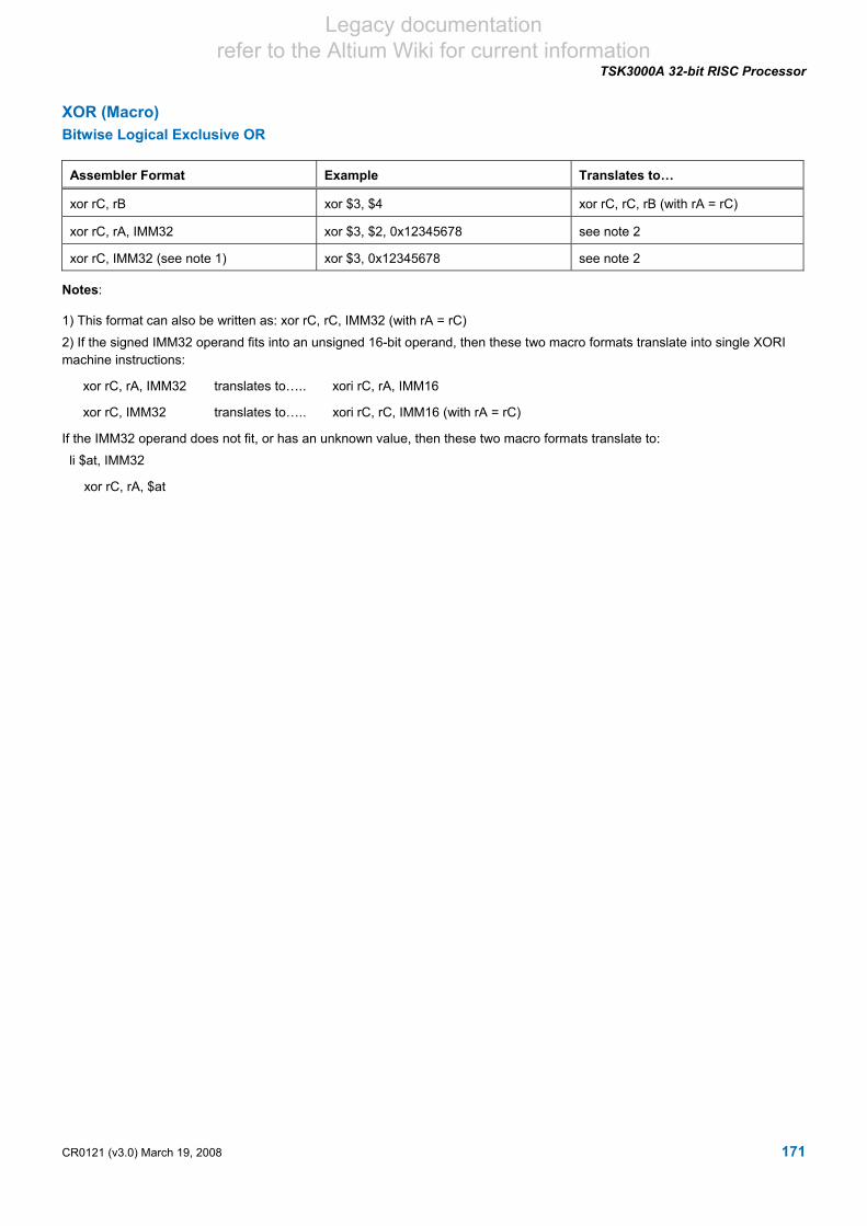
Legacy documentation refer to the Altium Wiki for current information
TSK3000A 32-bit RISC Processor
XOR (Macro) Bitwise Logical Exclusive OR
Assembler Format Example Translates to…
xor rC, rB xor $3, $4 xor rC, rC, rB (with rA = rC)
xor rC, rA, IMM32 xor $3, $2, 0x12345678 see note 2
xor rC, IMM32 (see note 1) xor $3, 0x12345678 see note 2
Notes:
1) This format can also be written as: xor rC, rC, IMM32 (with rA = rC)
2) If the signed IMM32 operand fits into an unsigned 16-bit operand, then these two macro formats translate into single XORI machine instructions:
xor rC, rA, IMM32 translates to….. xori rC, rA, IMM16
xor rC, IMM32 translates to….. xori rC, rC, IMM16 (with rA = rC)
If the IMM32 operand does not fit, or has an unknown value, then these two macro formats translate to:
li $at, IMM32
xor rC, rA, $at
CR0121 (v3.0) March 19, 2008 171

Legacy documentation refer to the Altium Wiki for current information
TSK3000A 32-bit RISC Processor
XORI Bitwise Logical Exclusive OR Immediate
Assembler Format: xori rB, rA, IMM16
Example: xori $3, $4, 0x1234
Description: Zero-extends the 16-bit immediate value, IMM16, bitwise logically exclusive-ORs it with the contents of GPR rA, then loads the result in GPR rB.
Operation: rC ← rA XOR ZeroExtend(IMM16)
Instruction Type: I-Type
Instruction Fields: rA = Register index of operand A
rC = Register index of destination
IMM16 = 16-bit immediate data value
Encoding:
31 30 29 28 27 26 25 24 23 22 21 20 19 18 17 16 15 14 13 12 11 10 9 8 7 6 5 4 3 2 1 0
0 0 1 1 1 0 rA rB IMM16
Latency: 1
172 CR0121 (v3.0) March 19, 2008

Legacy documentation refer to the Altium Wiki for current information
TSK3000A 32-bit RISC Processor
XORI (Macro) Bitwise Logical Exclusive OR Immediate
Assembler Format Example Translates to…
xori rC, IMM16 xori $3, oxFFFF xori rC, rC, IMM16 (where rA = rC)
CR0121 (v3.0) March 19, 2008 173

Legacy documentation refer to the Altium Wiki for current information
TSK3000A 32-bit RISC Processor
174 CR0121 (v3.0) March 19, 2008
Revision History
Date Version No. Revision
14-Dec-2004 1.0 New Release
04-Jan-2005 1.1 Updated information with respect to Programmable Interval Timer
08-Feb-2005 1.2 Modifications to debug panel information in On-Chip Debugging section.
09-May-2005 1.3 Updated for SP4
24-Jun-2005 1.4 Figures 10 and 28 updated, modifications in On-Chip Debugging section.
30-Sep-2005 1.5 TBH changed to TBHI in example for MFC0 instruction. Extent of vectored interrupt range corrected in text (from EB+01F8h to EB+00F8h)
12-Dec-2005 1.6 Path references updated for Altium Designer 6
15-Jul-2006 2.0 Updated for Altium Designer 6.4.
19-Mar-2008 3.0 Updated for Altium Designer Summer 08
Software, hardware, documentation and related materials:
Copyright © 2008 Altium Limited.
All rights reserved. You are permitted to print this document provided that (1) the use of such is for personal use only and will not be copied or posted on any network computer or broadcast in any media, and (2) no modifications of the document is made. Unauthorized duplication, in whole or part, of this document by any means, mechanical or electronic, including translation into another language, except for brief excerpts in published reviews, is prohibited without the express written permission of Altium Limited. Unauthorized duplication of this work may also be prohibited by local statute. Violators may be subject to both criminal and civil penalties, including fines and/or imprisonment. Altium, Altium Designer, Board Insight, Design Explorer, DXP, LiveDesign, NanoBoard, NanoTalk, P-CAD, SimCode, Situs, TASKING, and Topological Autorouting and their respective logos are trademarks or registered trademarks of Altium Limited or its subsidiaries. All other registered or unregistered trademarks referenced herein are the property of their respective owners and no trademark rights to the same are claimed.