rights / license: research collection in copyright - non ...28773/... · pd dr. h. hall,...
TRANSCRIPT

Research Collection
Doctoral Thesis
Micromachined platforms for manipulating and recording fromcells
Author(s): Greve, Frauke
Publication Date: 2006
Permanent Link: https://doi.org/10.3929/ethz-a-005207072
Rights / License: In Copyright - Non-Commercial Use Permitted
This page was generated automatically upon download from the ETH Zurich Research Collection. For moreinformation please consult the Terms of use.
ETH Library

DISS. ETH NO. 16526
MICROMACHINED PLATFORMS FOR MANIPULATING AND
RECORDING FROM CELLS
A dissertation submitted to the
SWISS FEDERAL INSTITUTE OF TECHNOLOGY ZURICH
For the degree of
Doctor of Technical Science
presented by
FRAUKE GREVE Dipl.-Ing. ETH Zurich
Born July 26, 1973 Citizen of Germany
accepted on the recommendation of
Prof. Dr. A. Hierlemann, examiner PD Dr. H. Hall, co-examiner
Prof. Dr. H. Baltes, co-examiner Prof. Dr. M. Koudelka-Hep, co-examiner
2006

Copyright © 2006 by Frauke Greve, Physical Electronics Laboratory
All rights reserved. No parts of the book may be reproduced, stored in a retrieval
system, or transmitted, in any form or by any means, electronic, mechanical,
photocopying, recording or otherwise, without the prior written permission of the
copyright holder.
Published by: Physical Electronics Laboratory ETH Zurich Wolfgang-Pauli-Str. 16 CH-8093 Zurich Switzerland

Contents | I
Table of Contents
1 Introduction...........................................................................................................1
1.1 Motivation of this work.................................................................................1
1.2 Structure of this thesis ...................................................................................3
1.2.1 First aspect: defined cell placement......................................................3
1.2.2 Second aspect: cell-electrode interface.................................................4
1.2.3 Further application of the cell-placement technique: parallel drug screening ...............................................................................................................6
1.3 Major achievements ......................................................................................7
1.3.1 Bio-electronic chip.................................................................................7
1.3.2 Cell-electrode interface .........................................................................8
1.3.3 Microchip-based cell-screening system ...............................................9
2 Background on microchip-based cell-monitoring systems............................. 11
2.1 Electrogenic cells........................................................................................ 11
2.1.1 Cell membrane .................................................................................... 12
2.1.2 The nervous system ............................................................................ 13
2.1.3 The neuron........................................................................................... 13
2.1.4 The action potential ............................................................................ 14
2.1.5 Dorsal root ganglia.............................................................................. 18
2.1.6 Cardiomyocytes .................................................................................. 20
2.2 Bio-electronic chips.................................................................................... 23
2.2.1 From intracellular to extracellular cell recording ............................. 23
2.2.2 Introduction to microelectrode arrays................................................ 26
2.2.3 From passive to active MEAs ............................................................ 29
2.2.4 Applications of MEAs ........................................................................ 31
2.3 Interface between cell and chip ................................................................. 33
2.3.1 Biological aspects ............................................................................... 33
2.3.2 Electrical aspects................................................................................. 41
3 Perforated CMOS microchip for immobilization and activity monitoring of electrogenic cells........................................................................................................ 47
3.1 Introduction................................................................................................. 47

3.2 Device description ...................................................................................... 50
3.2.1 CMOS circuitry................................................................................... 50
3.2.2 Microelectrodes................................................................................... 51
3.2.3 Cell-immobilization features.............................................................. 51
3.2.4 Packaging and setup ........................................................................... 51
3.3 Fabrication .................................................................................................. 52
3.3.1 Step 1: orifice etching......................................................................... 52
3.3.2 Step 2: lift-off process ........................................................................ 52
3.3.3 Step 3: passivation .............................................................................. 53
3.3.4 Step 4: electro-chemical etching........................................................ 53
3.3.5 Packaging ............................................................................................ 54
3.4 Experimental............................................................................................... 56
3.4.1 Cell culturing....................................................................................... 56
3.4.2 Chip preparation.................................................................................. 56
3.4.3 Cell placement..................................................................................... 57
3.5 Results and discussion................................................................................ 58
3.5.1 Electrical characterization .................................................................. 58
3.5.2 Cell recordings .................................................................................... 61
3.6 Conclusion .................................................................................................. 65
4 Molecular design of the neuron-to-CMOS interface....................................... 67
4.1 Introduction................................................................................................. 67
4.2 Experimental............................................................................................... 70
4.2.1 Surface modification with different adhesion-mediating proteins for neurite extension................................................................................................ 71
4.2.2 Visualization of the cell-to-chip interface ......................................... 73
4.3 Results & Discussion.................................................................................. 74
4.3.1 Measurements of neurite extension ................................................... 74
4.3.2 Network formation of single DRG neurons ...................................... 77
4.3.1 Visualization of the cell-to-electrode distance.................................. 81
4.4 Conclusion .................................................................................................. 87

Contents | III
5 Microchip High-Throughput Cell- Screening System with Integrated Dilution Stage............................................................................................................................ 89
5.1 Introduction................................................................................................. 89
5.2 Device description and modeling .............................................................. 91
5.2.1 Silicon orifice chip.............................................................................. 92
5.2.2 Microfluidic system............................................................................ 93
5.2.3 Design and modeling approach.......................................................... 95
5.3 Experimental............................................................................................... 99
5.3.1 Microchip fabrication ......................................................................... 99
5.3.2 Fabrication of the microfluidic device............................................. 100
5.3.3 Embedding of the silicon chip ......................................................... 101
5.3.4 External setup.................................................................................... 101
5.3.5 Chamber pretreatment ...................................................................... 102
5.3.6 Cell preparation................................................................................. 102
5.3.7 Cell loading ....................................................................................... 102
5.4 Results & Discussion................................................................................ 103
5.4.1 Validation of the drug diluter architecture ...................................... 103
5.4.2 Cell adhesion..................................................................................... 106
5.4.3 Drug screening experiments with cell trackers ............................... 107
5.5 Conclusion ................................................................................................ 109
6 Conclusion and Outlook.................................................................................. 111
6.1 Conclusion ................................................................................................ 111
6.2 Outlook...................................................................................................... 112
7 References ........................................................................................................ 115
8 Appendix .......................................................................................................... 121
8.1 Post-processing of the CMOS wafer ....................................................... 121
8.2 Staining protocol for neonatal rat cardiomyocytes (NRCs)................... 125
8.3 Biocompatibility Experiments ................................................................. 126
8.4 Processing of the SOI-wafer .................................................................... 128
8.5 Fabrication steps of the microfluidic chip............................................... 130

8.6 Cell-screening experiments using normal human dermal fibroblasts (NHDFs)............................................................................................................... 132
9 Acknowledgements ......................................................................................... 135
10 Publications...................................................................................................... 139
11 Curriculum Vitae ............................................................................................. 141

Abstract | V
Abstract
The application of microtechnological methods to biology provides an exciting new set of tools that can be used to, e.g., interact with and to record from cells. One main direction of research in this context comprises the development of mi-crochip-based cell monitoring systems. These devices contain living biological cells that show physiological changes upon exposure to, e.g., new candidate sub-stances for pharmaceutical applications. This thesis reports on the design and the fabrication of a bio-electronic CMOS chip with integrated on-chip read-out schemes and cell immobilization features. The 5×5 mm2 chip comprises sixteen 20×20 µm2 platinum electrodes, four high-pass filters (100 Hz cut-off), four multiplexers to select electrodes for readout, and four amplifiers with selectable gain (2×, 10×, 100×). In-house, post-CMOS proc-essing was used for both, the patterning of the transducer element (in this case platinum electrodes) and the realization of immobilization features for precise cell placement. The signal transduction is based on extracellular recording of the electrical activity of cultured cells by means of an array of microelectrodes (MEA). These electrodes cannot be fabricated using the CMOS-aluminum layers, as this metal is a neuro-toxicant and is not chemically inert. Therefore, platinum has to be deposited and patterned by lift-off during postprocessing to assure a defined and stable electrode surface. As the likelihood that all electrodes are occupied by cells is very small, a technique to precisely place cells onto the electrodes has been developed, which relies on a purely physical technique, the so-called ‘pneumatic anchoring’. Post-processing procedures, i.e., a combined electro-chemical and reactive-ion etching, have been used to equip the metal electrodes with small (3-µm diameter) through-the-wafer orifices. Thus, the cells could be dragged from a cell suspension onto these electrodes using a small underpressure applied from the backside of the chip. Neonatal rat cardiomyocytes have been immobilized this way and have been cul-tured for several days. Electrophysiological recordings have been performed on the one hand with conventionally plated cells and, on the other hand, with these individually immobilized cells. As a further interesting application of the physical immobilization technique, a hybrid microsystem was developed that is capable to perform all essential steps of a drug-screening process. The pneumatic anchoring is used to immobilize 1000 cells on a perforated membrane of a silicon chip. Then, drug dilution over three orders of magnitudes has been accomplished by developing a microfluidic cover

VI | Abstract
with integrated, cascading mixing channels. The whole unit, which constitutes a microchip-based cell-screening system, allowed for an incubation of the immobi-lized cells for several days, and for monitoring of the drug-induced physiological changes by fluorescence microscopy. High-quality, long-term recordings from neurons by means of microelectrode ar-rays can only be realized if the biological and the electrical interface between cell and electrode surface has been optimized by selecting an adequate adhesion-promoting protein. Therefore, the biological interface has been studied in experi-ments with embryonic chicken neurons from the dorsal root ganglia. Cell adhesion and proliferation on different adhesion proteins that have been coated on typical CMOS-surface layers were analyzed. Additionally, the interface morphology be-tween the cells and the electrode surface was characterized by scanning electron microscopy and transmission electron microscopy.

Zusammenfassung | VII
Zusammenfassung
Die vorliegende Doktor Arbeit beschreibt das Design und die Herstellung eines auf CMOS-Technologie-basierenden Mikroelectrodenarrays (MEAs). Der 5×5 mm2 grosse Chip besteht aus 16 Platinelektroden, 4 Hochpass-Filtern (100 Hz Grenzfrequenz), 4 Multiplexern zur Elektrodenauswahl und 4 verstellbaren Operationsverstärkern (2×, 10×, 100×). Elektrogene Zellen werden auf den Transducerelementen, den Elektroden, kultiviert, und deren elektrophysiologische Aktivität wird als Spannungsimpuls auf den Metallelektroden gemessen. Diese extrazelluläre Methode ermöglicht es, nichtinvasive Messungen über einen Zeitraum von Wochen oder Monaten durchzuführen, ohne die Zellen während des Messvorgangs zu verletzen. Eine Nachprozessierung der CMOS-Chips ist notwendig, um zwei Merkmale auf dem Chip zu integrieren: (1) strukturierte Platinelektroden und (2) die Perforation dieser Elektroden für eine präzise Platzierung der Zellen. Die Metallschichten des CMOS-Prozesses bestehen aus Aluminium, das unter physiologischen Bedingungen korrodiert und zudem neurotoxisch wirkt. Elektroden aus Platin hingegen sind biokompatibel und langzeitstabil. Die Prozessierung der Elektroden erfolgt über die Abscheidung einer Platinschicht und deren Strukturierung mit Hilfe eines Lift-off Prozesses. Die Signalstärke aktiver Zellen ist sehr gering (zwischen 10 und 1000 µV), weshalb gute Signalqualität nur dann erreicht werden kann, wenn sich die Zellen direkt auf der Elektrodenoberfläche befinden. Aus diesem Grund wurde eine Immobilisierungsmethode entwickelt, um individuelle Zellen direkt auf den Elektroden platzieren zu können. Mit Hilfe von CMOS-Prozessierungsschritten, die einen elektrochemischen Ätzstopp und ein Trockenätzverfahren beinhalten, wurden die Platinelektroden mit kleinen Löchern (3 µm) perforiert. Ein am Chip rückseitig angelegter Unterdruck zieht einzelne Zellen aus der Zellsuspension in Richtung der Elektrode und hilft, die Zelle direkt auf dieser zu immobilisieren. Mit Hilfe dieser physikalischen Immobilisierungs-methode, auch ’pneumatic anchoring’ genannt, gelang es, neonatale Herzmuskel-zellen von Ratten auf dem bio-elektronischen Chip zu platzieren, und deren elektrische Aktivität abzuleiten. Messungen mit einerseits konventionell kultivierten und andererseits immobilisierten Zellen wurden nach 4 Tagen in vitro durchgeführt. Signalamplituden von 500 µV und eine Signaldauer von ca. 2 ms konnten gemessen werden. Eine alternative Anwendung der Immobilisierung beinhaltete die Fabrikation eines Mikrosystems, das es ermöglicht, alle essentiellen Schritte eines ‚Drug-screening

VIII | Zusammenfassung
Prozesses’ durchzuführen. Das System basiert auf einem perforierten 5×7 mm2 grossen Siliziumchip, auf dem über 1000 Zellen geordnet platziert und über mehrere Tage inkubiert werden können. Der Chip ist in ein grösseres Elastomer mit kaskadierten, mikrofluidischen Kanälen eingebettet. Dieses Kanalsystem enthält Verdünnungsstufen und ermöglicht eine Konzentrationsvariation des Analyten über drei Grössenordnungen. Die verschiedenen Verdünnungen strömen in benachbarten, laminaren Flüssen über die Zellen. Die dadurch hervorgerufenen physiologischen Änderungen in den Zellen können mittels Fluoreszenzmikros-kopie gemessen werden. Die elektrische und biologische Schnittstelle zwischen Zelle und Elektrode sollte für die Kultivierung von Nervenzellen optimiert werden, um qualitativ hochwertige Langzeitmessungen zu ermöglichen. Dazu werden geeignete Adhäsionsschichten, CMOS-Passivierungsschichten und Metallschichten ausgewählt, die eine ausreichende Anhaftung and Differenzierung von Zellen gewährleisten. Als Modellsystem dienten Hühner-Nervenzellen aus dem Dorsal-Root-Ganglion (Rückenmarks-Ganglion). Diese wurden auf CMOS-Substraten kultiviert, auf denen verschiedene Proteine adsorbiert wurden. Die Morphologie der Grenzschicht wurde zusätzlich mit Rasterelektronen-Mikroskop- und Transmissions-Elektronenmikroskopaufnahmen analysiert, um das Interface zwischen der Zelle und dem Substrat zu charakterisieren.

Introduction | 1
1 Introduction 1.1 Motivation of this work In 1771, Luigi Galvani (1737-1798) noticed an unexpected reaction when a frog leg came in contact to a spark from a machine: the frog’s leg kicked as it would be alive (Figure 1-1). Galvani repeated the experiment by setting a frog’s leg between two different metals and saw the muscles of the leg contracted again. He believed that the reaction originated from the frog itself and called this phenomenon ‘ani-mal electricity’. Volta, a close friend of Galvani, discovered later the origin of ‘animal electricity’ and thereby invented the first battery. As Galvani was the first to see a relationship between electricity and animation, he is typically credited with the discovery of ‘bioelectricity’.
Figure 1-1: Illustration of the experiment, in which Galvani showed that the nerve of the frog was excited by an electric atmospheric discharge created by his generator. (Credit: Dall'opera ‘De viribus electricitatis in motu musculari commentarius’) (ScienzaGiovane).

2 | Chapter 1
Galvani’s experiments over two hundred years ago triggered a widespread and ever increasing interest in electrophysiology, the science of physiology that deals with the flow of ions and the resulting potential changes in biological tissues. Re-searchers are in particular interested in electrophysiological recording techniques that enable to get a better insight and to understand interactions within the com-plex cellular networks in living organisms. At the same time, also the stimulation of muscles and nerve cells is of great interest. Nowadays, biomedical engineering has advanced this scientific frontier to a point, where stimulation devices are implemented by standard surgery: Pacemakers regu-late the beating of the heart, implants improve impaired hearing by stimulation electrodes inside the cochlea, and implanted brain pacemakers help to treat dis-eases such as epilepsy or Parkinson. For a better understanding of the interactions of cellular networks, researchers had to narrow the focus of their investigations from whole tissue like Galvani’s frog leg to tissue slices and finally to single cells. This last step was significantly facili-tated by the advent of miniaturized systems with two- or three-dimensional elec-trode arrays for recording and stimulation. These so-called bio-electronic or micro-electrode array chips were first published in the 1970s by Wise, Thomas, Gross and Pine. These days, two-dimensional microelectrode arrays are widely used for long-term extracellular, electrophysiological characterization of cell cultures. Chips with integrated recording and stimulation capabilities as well as with on-chip multiplexers and signal conditioning units have been developed. Even com-mercial solutions are available. Although these bio-electronic chips are a powerful tool, the extracellular meas-urements are carried out in vitro, which requires the dissociation of cells from their natural environment followed by artificially re-establishing the cellular networks on-chip. As a result, a thorough understanding of the interpretation of the recorded data and their biological relevance is necessary. Additionally, the transfer of the cells onto the chip surface requires biological and technical knowledge, methods and tools to assure stable long-term measurements. The issue of transferring and culturing cells on a chip and the investigation of the cell-to-electrode interface constitute the central aspects of this thesis: 1. In typical experiments, the likelihood of placing cells on all electrodes is very
small. Therefore, a reliable method to place cells on micro-electrode arrays (MEAs) would be desirable to achieve reproducible experimental boundary conditions.

Introduction | 3
2. For stable, long-term measurements, the biological and electrical interface be-tween the cell and the electrode of the bio-electronic chip has to be optimized.
1.2 Structure of this thesis
1.2.1 First aspect: defined cell placement
A number of academic and industrial research groups worldwide strive to enhance the electrical characteristics of MEAs. However, the focus of this present work was not the design of a new electrical system, but rather the development of a new feature to improve the chip functionality generally: To be able to perform more efficient extracellular recording, it would be beneficial if the cultured cells (neu-rons or other electrogenic cells) were precisely placed onto the electrode sites. To this end, a purely physical immobilization technique for efficiently and auto-matically placing cells on electrodes was developed. Small orifices (3 µm in di-ameter) in the silicon chip were used for pneumatic anchoring the cells by apply-ing a small underpressure from the backside of the chip. Cells were guided from a cell suspension to the holes in the silicon substrate and could therefore be directly immobilized on the electrodes (Figure 1-2). The cells adhered to the substrate, which had been coated beforehand with an adhesion-promoting protein layer, and could then be cultured for several days. This pneumatic anchoring technique has considerable advantages, such as straightforward, wafer-level implementation by mature micromachining techniques, compatibility with a wide range of substrates and technologies, and purely passive, highly parallel operation. As proof of con-cept, immobilization experiments were performed with fibroblasts on silicon-on-insulator chips, and later, with neonatal rat cardiomyocytes (NRCs) on a specially designed, perforated bio-electronic chip.

4 | Chapter 1
Papplied
PambSolution
Cell
ProteinCell
no flow
Immobilized cell Good seal
Figure 1-2: Concept of the immobilization technique: a small underpressure is applied from the backside of the chip (left), and cells are dragged from a suspension to the orifices (right).
This bio-electronic chip was fabricated using a CMOS (complementary metal-oxide semiconductor) process, a widely used technology for fabricating applica-tion-specific integrated circuits. The chip comprised 16 platinum electrodes with orifices, on-chip multiplexers, high-pass filters and amplifiers. Further amplifica-tion and low-pass filtering was performed off-chip. The multiplexers were inte-grated on-chip to illustrate the capabilities of this technology to address larger numbers of electrodes (e.g., hundreds). Neonatal rat cardiomyocytes were used in this experiment as they generate strong electrical signals already after a short time in culture. The contraction of the cardiac muscle cells is optically observable, and the diameter of the cell bodies, ca. 20 µm, is suitable for pneumatic anchoring on the 3-µm orifices. Immobilization and electrophysiological experiments were performed to demon-strate the extracellular recording from immobilized cells. Signals of convention-ally plated cells and immobilized cells were recorded and compared.
1.2.2 Second aspect: cell-electrode interface
Cells need to attach to the electrode surface to be able to adhere and proliferate. This interface is of high importance for biological and electrical aspects of MEA technology. From the biological point of view, it is essential that cells are able to specifically bind to the chip surface. One possible way to promote cell adhesion is to adsorb the chip surface with a layer of cell-adhesive proteins. To guarantee good cell ad-hesion, these proteins have to be chosen carefully and in agreement with the cell

Introduction | 5
type to be used. Generally, this requires a thorough understanding and characteri-zation of the cell-to-electrode interface. Hence, important issues in this context are the biocompatibility of the different CMOS layers and the selection of a suitable adhesion-promoting protein. To characterize biocompatibility and adhesion properties of different adhesion layers, a technique to quantitatively analyze the neuronal outgrowth of neurons from dorsal root ganglia (DRG) was developed. The neurons were cultured for several days on the CMOS surfaces coated with different adhesion proteins, and the neurite outgrowth was determined. Furthermore, as the neurons are supposed to be cultured for several weeks on bio-electronic chips, the proliferation of fibro-blasts has to be inhibited. Therefore, experiments with cytosine ß-D-arabinofuranoside (AraC) were performed to restrain the number of fibroblasts. From the electrical point of view, it is important to assure a good transmission of the electrical signal through the complex bio-physical interface chain from cell membrane to protein layer to electrode. Two components describe the electrical connection between the cell and the measurement system: (a) the signal is guided through a capacitive component (Ccoup) into the electrode, and (b) a part of the sig-nal is lost to the surrounding medium by a parasitic, resistive component (Rseal).
Pt electrode
VrefCcoup
Rseal
Cell
Figure 1-3: Electrical connection between cell and measurement system, (a) coupling capacitance Ccoup, and (b) sealing resistance Rseal.
It is desirable to achieve a high coupling capacitance by a thin protein layer and a minimum gap between cell membrane and protein layer. Additionally, it is benefi-cial if a maximum fraction of the electrode area is covered by the cell. At the same time, a high parasitic resistance prevents undesired diffusion of ions away from the electrode. Also the sealing resistance depends on the electrode coverage and the

6 | Chapter 1
gap between the membrane and the electrode. Thus, it is generally advantageous for the optimization of both, Rseal and Ccoup, to achieve a minimum interfacial gap and maximum electrode coverage. The latter one is assured by the pneumatic an-choring technique, while the first depends strongly on the selection of the adhesion protein. Therefore, distance measurements between cells and electrodes were performed with a scanning-electron microscope (SEM) and a transmission-electron micro-scope (TEM) to further analyze the interface properties when using different adhe-sion layers. These methods helped to analyze the cell-substrate interface with the aim to achieve (a) stable, long-term cultures and (b) a satisfactory signal-to-noise ratio of the recorded extracellular signals of electrogenic cells.
1.2.3 Further application of the cell-placement technique: parallel drug screening
Living cells are powerful biosensors capable of analyzing complex sample mix-tures and responding physiologically to them. As the physical immobilization technique described earlier is not only applicable to electrophysiological experi-ments, it is also a valuable method to immobilize large cell populations for cell-based biosensing and drug screening. To illustrate this, a chip capable of immobilizing 1000 single cells in less than 30 seconds with the pneumatic anchoring technique was used for drug screening over a concentration range of three orders of magnitude. A cell array of reproduci-ble and defined arrangement was obtained, which also allowed cell culturing for several days. The pneumatic trapping and immobilization of cells was performed using a silicon-on-insulator (SOI) chip embedded into a larger microfluidic elas-tomer substrate. Five different drug concentrations were provided by a microflu-idic unit with an integrated, cascaded drug diluter. The system also featured an in-cubation chamber for the immobilized cells. A simultaneous application of differ-ent drug concentrations in the same culturing chamber and under the same cultur-ing conditions was thus possible. The drugs were directed over the cells in laminar streams and diffused through the cell membrane into the cells. The drug-induced effects on the immobilized cells could be optically monitored by using reporter molecules, which were fluorescently labeled. This system could be used for all essential steps of the drug screening process: (I) the immobilization of a defined number of cells in a homogeneous array, (II)

Introduction | 7
the drug dilution, (III) the incubation over several days inside a 0.5 µl incubation chamber and (IV) the optical read-out using a fluorescence microscope.
1.3 Major achievements
1.3.1 Bio-electronic chip
Development of a new physical method to reliably place and immobilize cells. The cells were immobilized on the chip surface in a defined pattern by means of etched orifices through the chip and by applying slight suction to attract cells from a suspension (Figure 1-4). It was proven that pneumatic anchoring is gentle enough to retain the structural integrity as well as the function of the immobilized cells. As proof of concept, the pneumatic-anchoring method was successfully imple-mented on an active bio-electronic microelectrode-array chip designed and fab-ricated for this purpose. The chip was based on a commercial CMOS process and featured integrated signal-processing units including multiplexers, amplifiers and high-pass filters. Orifices for cell immobilization and platinum electrodes were fabricated by dedicated post-processing steps developed in this thesis.
Figure 1-4: Immobilized cardiomyocytes on perforated platinum electrodes (left), and extracellular recordings of the immobilized cells (right).
0.5 ms
1 mV

8 | Chapter 1
Measurement results obtained with this successful combination of a CMOS-MEA with pneumatic anchoring are illustrated in Figure 1-4 (right), which shows action potentials of neonatal rat cardiomyocytes extracellularly monitored by this system.
1.3.2 Cell-electrode interface
A systematic study of cell adhesion and growth on a variety of combinations of adhesion-protein layers and CMOS material layers was carried out with the goal to find optimum culturing conditions on MEA chips. The optimization has been performed with regard to neurite outgrowth as an indicator for biocompatibility (Figure 1-5, left), distance between cell and substrate to ensure good electrical coupling (Figure 1-5, right), and reduction of undesired fibroblast proliferation. Over 300 samples were evaluated using optical and electron microscopy. Suitable proteins and the corresponding culturing conditions were identified and effectively applied in the cell-monitoring studies presented in this thesis.
Figure 1-5: Chicken dorsal root ganglion cultured on a laminin-1-coated platinum chip for two days (left), transmission-electron-microscope micro-graph to determine the distance between cell- and electrode surface (right).
Cell layers
Protein (L1Ig6) layer
Platinum surface
200 µm

Introduction | 9
1.3.3 Microchip-based cell-screening system
The concept of pneumatic anchoring was used to simultaneously and automati-cally form arrays of thousand cells on a planar substrate for applications like drug screening or biosensing. A fully-integrated drug-screening system (Figure 1-6) was developed, which includes a cell-immobilization unit, a polymer-based incubation chamber, a dilution cascade for preparing drug concentrations over three orders of magnitude, and optical readout accessibility by using fluorescent reporter molecules. An exemplary drug-screening experiment using a fluorescent cell tracker and normal human dermal fibroblasts (NHDFs) was performed to illustrate the opera-tion of this device. This hybrid polymer/silicon device illustrates the rich function-ality possible with a combination of silicon-based precision micromachining and low-cost polymer replication.
Figure 1-6: Micro-graph of the cell-screening system with an on-chip diluter, the 0.5-µl incubation chamber and the cell-loading ports (scale bar: 1 cm).
Drug inlet Buffer inlet
Cell loading ports
Incubation chamber


Background on microchip-based cell-monitoring systems | 11
2 Background on microchip-based cell-monitoring systems
The subject of this thesis, a silicon-microchip-based monitoring system for bio-logical cells, is inherently interdisciplinary. This background chapter is intended to provide the reader with the fundamentals of cell biology and engineering as re-quired for the following chapters. Microchips can be used to monitor different physical or chemical cell parameters. The recording of electrical signals generated by electrogenic cell types is a very convenient way to monitor the corresponding cell activity. Due to their importance for basic research as well as for pharmaceutical applications, these organisms re-ceive significant attention by the scientific community. Neurons and cardiomyocytes are the two most prominent examples of electrogenic cells that are described here along with the generation of electrical signals, so-called ‘action potentials’. The electrical signals can be recorded by means of bio-electronic chips, as will be detailed in subsequent sections. Finally, the cell-chip interface is described with emphasis on cell adhesion and electrical signal re-cording via electrodes in an aqueous environment. Both aspects are of importance to optimize the experimental conditions for electrical cell activity monitoring.
2.1 Electrogenic cells Cells that are able to produce spontaneous electrical activity by generating large changes in their membrane potential are called electrogenic cells. This study con-centrates on two types of electrogenic cells, neurons and cardiomyocytes, which form vastly different types of cellular networks. Neurons, on the one hand, de-velop into strongly interacting networks for signal transmission and processing. Signals are transferred between the respective neurons by efficient synaptic inter-faces. Cardiomyocytes, on the other hand, are contracting muscle cells, which are connected to neighboring cells via protein gap junctions in order to produce syn-chronized mechanical activity.

12 | Chapter 2
Both cell types allow for studying spontaneous electrical activity as well as the re-sponse behavior upon stimulation or drug exposure. Neurons facilitate the investi-gation of information transmission, storage and processing procedures, whereas cardiomyocytes enable research into signal propagation and synchronization strategies. The following pages touch on the most important aspects of electrogenic cells in a compact form. The focus is primarily on the cell types used in the research re-ported on here, i.e., dorsal root ganglia and rat cardiomyocytes.
2.1.1 Cell membrane
The selectively permeable cell membrane (Figure 2-1) is a thin and structured bi-layer of phospholipids and protein molecules. It separates the cytoplasm from its surrounding and the embedded ion channels regulate the transport of molecules in and out of the cell. The cell membrane features a variety of proteins that can, e.g., act as anchoring sites for the cytoskeleton or for components of the extracellular matrix. The transport of molecules across the membrane is either passive as small or lipophilic molecules can freely diffuse across the membrane or it is active, i.e., molecules are transported through the membrane against a concentration gradient by means of membrane pumps.
Figure 2-1: Sketch of a cell membrane (Alberts, Johnson et al. 2002).

Background on microchip-based cell-monitoring systems | 13
2.1.2 The nervous system
The nervous system is a highly branched signaling network, which regulates all aspects of functions in the body. The nervous system consists of the central nerv-ous system (CNS) including the brain and the spinal cord, and the peripheral nerv-ous system (PNS), which connects the CNS to the peripheral parts of the body. The human brain, the control center of the nervous system, contains about 1012 neurons, each forming as many as thousand connections with other neurons. The functions of these neurons are diverse: Sensory neurons, for example, have specialized receptors that convert different types of stimuli from the outside world (e.g. light, touch) into electrical signals and convey the information to the CNS, where this information is processed and reacted upon. Interneurons in contrast only communicate with other neurons and are mainly located in the brain. The outgoing information or actuation signal from the CNS is transmitted to muscle-stimulating motor neurons, which stimulate other types of cells such as muscle or gland cells, which react upon the stimuli.
2.1.3 The neuron
The smallest functional unit of the nervous system is the neuron. A neuron (Figure 2-2) usually consists of a cell body with the nucleus and other components; the in-coming information is received via highly branched processes, the dendrites, and directed towards the cell body. There, the signals are integrated and weighted and eventually provoke a cellular activity or response. An action potential is triggered if the membrane potential of the neuron is depolarized beyond a certain threshold. The outgoing signals are transmitted from the cell body via the axons to other neu-rons. A neuron may have many dendrites but it has, in most cases, only one axon, which can be much longer than the dendrites. The region with the highest signal density is called the axon hillock, where the axon leaves the cell body. The signal transmission from one neuron to another occurs via synapses. Synapses are specialized cell junctions, which enable the communication between different neurons and transfer the signals from the presynaptic axon terminal to postsynaptic dendrites. There are two different types of synapses, electrical and chemical synapses. Electrical synapses enable the spreading of an action potential from the presynaptic to the postsynaptic neuron via electrical gap junctions. These voltage-gated gap junctions are intercellular channels that allow the local ion cur-rents to flow between the neurons. In chemical synapses, however, the presynaptic cell is separated from the postsynaptic cell by the synaptic cleft. When an action potential occurs, the electrical signal of the arriving action potential is converted

14 | Chapter 2
into a chemical signal, i.e., the release of neurotransmitters. The neurotransmitter molecules diffuse across the synaptic cleft and bind to their appropriate receptor sites of the postsynaptic membrane. There, they trigger the opening of ion chan-nels so that the membrane depolarizes and an action potential in the postsynaptic neuron is evoked (Campbell and Reece 2002).
Figure 2-2: Sketch of the structure of a neuron. The incoming signals are di-rected via the dendrites towards the cell body. Upon signal arrival at the syn-apse, neurotransmitters are released that bind to the receptor sites of the postsynaptic cell. There, they trigger an action potential if the cell is depolar-ized beyond a certain threshold. (Campbell and Reece 2002).
2.1.4 The action potential
Each cell features an electrochemical-potential difference across the cell mem-brane, which is called the membrane potential. This difference is a consequence of an unequal distribution of predominantly sodium and potassium ions between the cytoplasm and the extracellular surrounding of the neuron (Figure 2-3 shows a simplified sketch of a cell membrane). This unequal distribution of ions is main-tained by a complex interplay of passive diffusion via ion-selective sodium-, po-tassium- and chloride channels complemented by active ion transport by the so-dium-potassium pump. The ion-selective channels permit ion transport along the electrical-field- and chemical-concentration gradients. A potassium equilibrium is established by competing ion fluxes out of the cell (due to a chemical concentra-tion gradient of 140 mM inside versus 4 mM outside) and into the cell (due to an electrical gradient of -70 mV). This potential difference is additionally maintained by a flux of negatively charged chloride ions in the opposite direction due to the

Background on microchip-based cell-monitoring systems | 15
inverse concentration gradient. For sodium, however, both, the concentration- and the potential gradient point into the same direction generating a constant flow of sodium into the cell. In spite of the similar magnitude of these concentration gra-dients, the sodium and the chloride flux are about ten times smaller than that of the potassium as a consequence of the lower sodium permeability (in this case, the permeability is proportional to the density of open channels in the cell membrane).
Figure 2-3: Simplified schematic of the ion distribution across the cell mem-brane of a neuron. In the resting neuron, about ten times more potassium channels are than sodium- or chlorine channels. As a consequence, there is a net positive charge relative to the inside of the cell (Lodish, Berk et al.).
Without any cellular activities, this would lead to a constant increase of sodium in the cell, which is accompanied by a reduction of the cytosolic potassium concen-tration. However, the ATP-driven sodium-potassium pump is capable of maintain-

16 | Chapter 2
ing the unequal ion distribution by transporting sodium- and potassium ions against their concentration gradient across the membrane. The processes described above lead to a resting potential of about -70 mV (relative to the outside of the cell). When an action potential occurs (Figure 2-4), a stimulus opens a few voltage-gated sodium channels in the membrane. Sodium ions diffuse along their concentration gradient into the cell, rendering the membrane potential more positive. If the sodium influx achieves a certain threshold potential (typically about -50 to -55 mV), an action potential is triggered. Additional sodium channels open, allowing even more sodium ions to enter the cytoplasm. The ion influx fur-ther depolarizes the membrane and within a fraction of a millisecond, the electrical potential in the local region of the membrane has shifted its potential to about +35 mV. At this point, the electrochemical driving force for sodium ions ap-proaches zero. A reversal of the action potential is initiated by closing and inacti-vating the sodium ion channels and opening the voltage-gated potassium channels. Potassium ions flow down their concentration gradient out of the cell, thereby re-polarizing the cell membrane. As the membrane potential returns to its resting state, the voltage-gated potassium channels start closing again. As they have rela-tively slow gates, the excessive potassium-ion flux causes the membrane potential to become more negative than the resting potential for a brief period (hyperpolari-zation or overshoot).

Background on microchip-based cell-monitoring systems | 17
Figure 2-4: The occurrence of a neuronal action potential with the corre-sponding sodium and potassium membrane conductances. The conductance for a specific ion is the result of the effective number of open ion channels for that particular ion (Morefield, Keefer et al.).
After an action potential occurred, there is a brief refractory period, during which the membrane cannot be depolarized. The action potential is an all-or-nothing event meaning that the amplitude is unaffected by the intensity of the stimulus. The nervous system, however, can distinguish between stronger and weaker sig-nals. Stronger signals produce action potentials at a higher frequency than weaker signals. Neurons can produce action potentials as rapidly as the refractory period will allow, which is approximately 1 ms (Alberts, Johnson et al. 2002; Campbell and Reece 2002). An action potential propagates along an axon towards other cells. Traveling along the axons means a continuous and unidirectional depolarization of neighboring re-gions of the cell membrane. The axons of many vertebrate neurons are insulated by a myelin sheath, which greatly increases the rate, at which an axon can conduct an action potential. The myelin sheath is formed by supporting cells, so-called glia cells, which are wrapped around the axon. The myelin-producing glia cells of the CNS are the oligodendrocytes and astrocytes, whereas those of the PNS are the Schwann cells.

18 | Chapter 2
Figure 2-5: In the peripheral nervous system, supporting cells, called Schwann cells, wrap around many axons forming an insulating myelin sheath. The gaps between successive Schwann cells are called the nodes of Ranvier. Only at these nodes, an action potential can be formed.
The myelin sheath of the peripheral neurons is interrupted at small gaps between successive Schwann cells along the axon, so-called nodes of Ranvier (Figure 2-5). At these nodes, most of the voltage-gated ion channels that produce the action po-tential are concentrated. As the myelinated regions of the axons have excellent iso-lation properties, a depolarization of the membrane at one node almost immedi-ately spreads passively to the next node, where it stimulates depolarization. This mechanism is called saltatory conduction, because the action potential seems to jump along the axon. This type of conduction has two main advantages: fast trav-eling of the action potential, as saltatory conduction can transmit impulses at speeds up to 150 m/sec, and conserving metabolic energy as the active excitation is confined to the nodes of Ranvier (Alberts, Johnson et al. 2002; Campbell and Reece 2002). This is especially important for the neurons of the peripheral nervous system, as they make projections to the far end of the hands and legs and can be as long as 1 meter or more. Therefore, fast nerve signal conduction is of major im-portance.
2.1.5 Dorsal root ganglia
The peripheral nervous system connects the CNS (brain and spinal cord) to the rest of the body. Three different types of neurons are involved: motor neurons, sensory neurons and interneurons. The cell bodies of the motor neurons and of the in-terneurons are located in the CNS, while the cell bodies of the sensory neurons are located in the dorsal root ganglia (DRG). The DRGs are nerve cell clusters of the
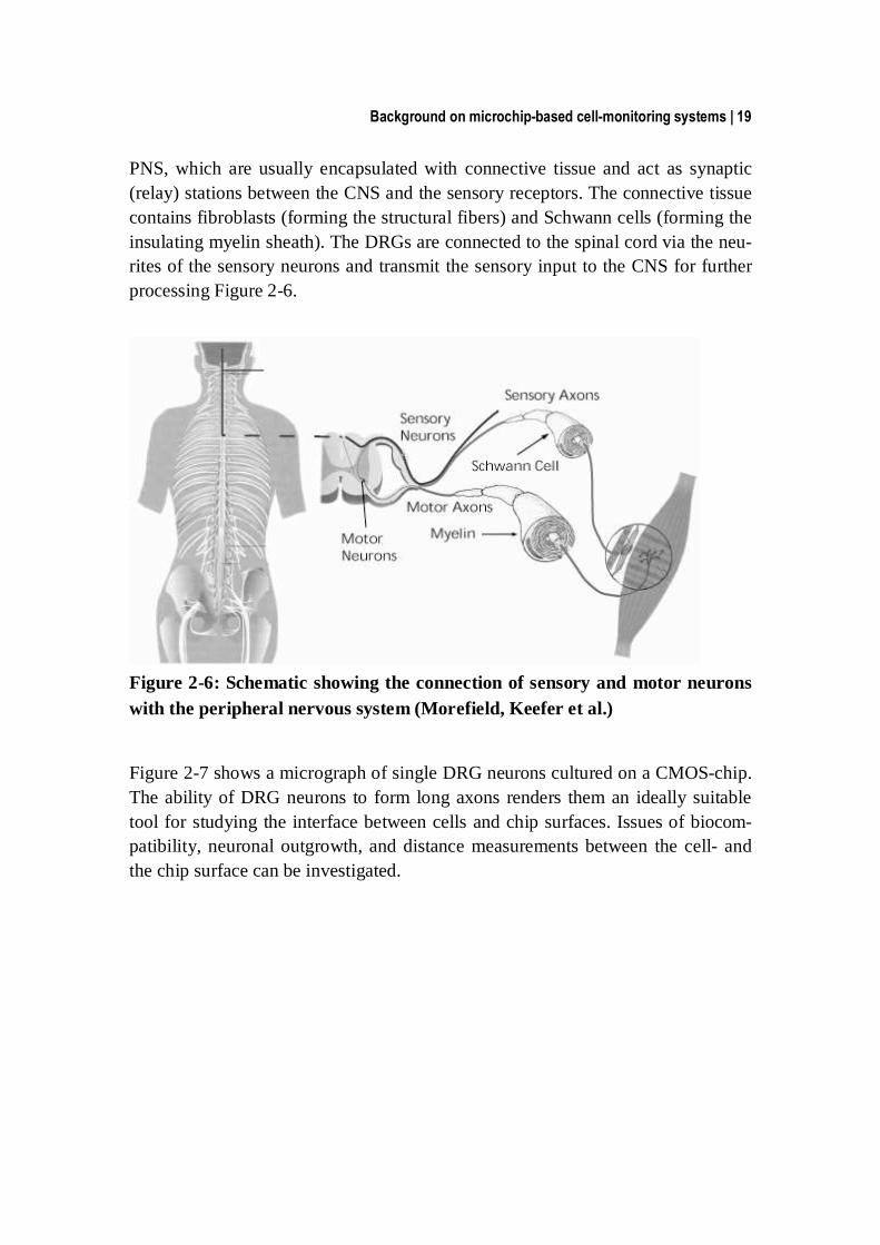
Background on microchip-based cell-monitoring systems | 19
PNS, which are usually encapsulated with connective tissue and act as synaptic (relay) stations between the CNS and the sensory receptors. The connective tissue contains fibroblasts (forming the structural fibers) and Schwann cells (forming the insulating myelin sheath). The DRGs are connected to the spinal cord via the neu-rites of the sensory neurons and transmit the sensory input to the CNS for further processing Figure 2-6.
Figure 2-6: Schematic showing the connection of sensory and motor neurons with the peripheral nervous system (Morefield, Keefer et al.)
Figure 2-7 shows a micrograph of single DRG neurons cultured on a CMOS-chip. The ability of DRG neurons to form long axons renders them an ideally suitable tool for studying the interface between cells and chip surfaces. Issues of biocom-patibility, neuronal outgrowth, and distance measurements between the cell- and the chip surface can be investigated.

20 | Chapter 2
Figure 2-7: SEM micrograph of a DRG neuron on a CMOS chip after 4 days in culture (scale bar 6 µm).
2.1.6 Cardiomyocytes
The electrical stimulus to produce a heartbeat is generated by the heart itself. The cells that create these rhythmical impulses are called pacemaker cells and control the heartbeat rate. Cardiac pacemaker cells are found in the sinoatrial and atrioven-tricular nodes of the heart and spontaneously generate action potentials at about 70-80 beats/minute. Non-pacemaker cells also contract spontaneously, however, at a much lower frequency (ca. 30-40 beats/minute). As the pacemaker cells release electrical pulses more frequently, they trigger the other cells and therefore syn-chronize the contraction of the whole heart. The pacemaker cell’s ability of producing an action potential is caused by sponta-neous depolarization, which is generated without any influence from neighboring cells (unlike neurons or muscles). The resting potential of cardiac cells is caused by a continuous efflux of potassium ions out of the cell and an influx of sodium ions into the cell. With increasing time, though, the potassium permeability de-creases causing a slow depolarization of the cell (the cytoplasm gets more posi-tive). This depolarization continues until the threshold potential (-40 mV to -50 mV) is reached, which causes calcium ions to diffuse into the cell by the open-ing of voltage-sensitive calcium channels. Repolarization of the pacemaker cells is initiated by closing the calcium channels and decreasing the sodium permeability.
Background on microchip-based cell-monitoring systems | 21
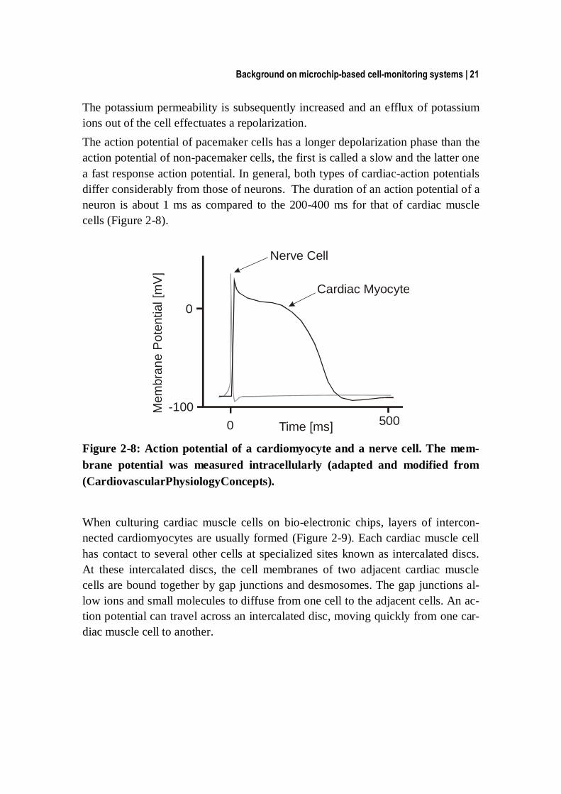
The potassium permeability is subsequently increased and an efflux of potassium ions out of the cell effectuates a repolarization. The action potential of pacemaker cells has a longer depolarization phase than the action potential of non-pacemaker cells, the first is called a slow and the latter one a fast response action potential. In general, both types of cardiac-action potentials differ considerably from those of neurons. The duration of an action potential of a neuron is about 1 ms as compared to the 200-400 ms for that of cardiac muscle cells (Figure 2-8).
Mem
bran
e P
oten
tial [
mV
]
-100500
0
0 Time [ms]
Cardiac Myocyte
Nerve Cell
Figure 2-8: Action potential of a cardiomyocyte and a nerve cell. The mem-brane potential was measured intracellularly (adapted and modified from (CardiovascularPhysiologyConcepts).
When culturing cardiac muscle cells on bio-electronic chips, layers of intercon-nected cardiomyocytes are usually formed (Figure 2-9). Each cardiac muscle cell has contact to several other cells at specialized sites known as intercalated discs. At these intercalated discs, the cell membranes of two adjacent cardiac muscle cells are bound together by gap junctions and desmosomes. The gap junctions al-low ions and small molecules to diffuse from one cell to the adjacent cells. An ac-tion potential can travel across an intercalated disc, moving quickly from one car-diac muscle cell to another.

22 | Chapter 2
Figure 2-9: Neonatal rat cardiomyocytes cultured on a bio-electronic chip af-ter 4 days in vitro.
100 µm

Background on microchip-based cell-monitoring systems | 23
2.2 Bio-electronic chips
2.2.1 From intracellular to extracellular cell recording
The biological and medical importance of electrogenic cells calls for a detailed analysis of the flow of ions and the resulting potential changes across the cell membrane. This research has been pioneered by Kenneth Cole in the 1930s, who was for the first time able to measure action potentials and the membrane conduc-tance of giant squid neurons using micropipette electrodes. Membrane potentials can be directly recorded by using one microlectrode inserted into the cell and one that remains external. The potential difference is amplified by a high-impedance electronic amplifier (current-clamp technique). A second meas-urement approach is voltage clamping, which allows maintaining a constant poten-tial across the membrane, while recording the transmembrane current. The poten-tial control is achieved by a negative-feedback amplification loop, which also serves as a current-to-voltage converter. Since nearly three decades, the patch-clamp technique, a variation of voltage-clamping, has been the gold standard for electrophysiological measurements. This technique allows to monitor the ion flux through the ion channels of a cell mem-brane. Different from earlier techniques, a glass micropipette ( > 1 µm), with a smooth tip surface is used instead of a microelectrode. The patch-clamp pipette contains an electrolyte and is affixed to the cell membrane by applying gentle suc-tion. The circular tip of the pipette thus insulates a defined region of the cell mem-brane (the patch) for electrophysiological studies. Due to the smooth surface a tight seal is formed between the electrolyte in the pipette and the extracellular me-dium leading to an electrical resistance in the G range. In essence, this gigaseal assures that leakage currents across the seal are negligible and, in some cases, the charge transfer through a single ion channel can be monitored. Patch-clamping can be performed on patches of a cell membrane still attached to the cell (cell-attached recording) or on fragments removed from the cell (excised patch). A third variant involves the rupture of the cell membrane by strong suction, while the pipette re-mains attached to the cell. This whole-cell recording technique allows monitoring the net-charge flow in and out of the cell. Especially interesting in the context of this work is the possibility of monitoring the action potentials of electrogenic cells. The patch-clamp technique is widely used by electrophysiologists for single-cell studies, but also to study cell-to-cell interactions. The patch-clamp technique was invented by Bert Sakmann and Erwin

24 | Chapter 2
Neher 1976 who received the Nobel Prize in 1992 for this achievement and their work on ‘the function of single ion channels in cells’.
(a)
(b)
Vbias
Cell
Patchelectrode
Referenceelectrode
R
VVI
Figure 2-10: (a) Photograph of a cell body of a cultured neuron and the tip of a patch pipette touching the cell membrane. (b) Basic patch-clamping ar-rangement for measuring the current flow through individual ion channels in the plasma membrane. The second electrode remains outside the cell (Lodish, Berk et al.).
Patch-clamp is a mature and well-established technique and as a consequence data interpretation is well understood. The drawback however is that the cells get dam-aged by the micropipette so that the patch-clamp technique cannot be used for

Background on microchip-based cell-monitoring systems | 25
long-term recording. Additionally, patch-clamp is a low-throughput technique as only a few cells can be patched simultaneously. Alternatively, the action potential of electrogenic cells can also be monitored by having electrodes exclusively in the extracellular space. Thus, the cells remain completely intact, and non-invasive measurements can be performed during sev-eral weeks or months. When an action potential in a cell occurs, a transient chan-nel opening allows positively charged sodium ions to move down the concentra-tion gradient into the cell. These moving ions or charges in the electrode vicinity evoke potentials on the electrodes, which lead to a transient voltage change be-tween the measurement and the counter electrode of the setup (Figure 2-11). Gen-erally, extracellular measurements yield signals that are by a factor of approxi-mately 1000 lower than those recorded by intracellular methods. Dedicated read-out electronics, though, are capable of recording these signals with good signal-to-noise ratio.
Passivationlayer
Counterelectrode
MeasurementelectrodeCell
Amplifier
Figure 2-11: Schematic of an extracellular measurement setup.
A significant advantage of the extracellular method over the patch-clamp tech-nique is the possibility of fabricating two-dimensional arrays of many miniaturized electrodes, which are similar in size to a typical cell (Figure 2-12). This allows for simultaneous recording from tens to hundreds of cells without damaging the cells. As the signal strength of an extracellularly recorded signal is comparatively small, only cells that are placed very close to the electrode site are recorded from.

26 | Chapter 2
Figure 2-12: DRG neurons cultured on platinum metal electrodes on a silicon chip. The non-electrode area is covered by an insulating silicon-nitride layer.
2.2.2 Introduction to microelectrode arrays
A microelectrode array or MEA is an arrangement of microelectrodes of typically up to 60 to 100 electrodes, which allows for extracellular recording and, in some cases, also for stimulation of electrically active cells. The MEAs can be used for studying the interaction of dissociated cell cultures as well as for organotypic slices and whole-heart studies. As the cells are not damaged during the measure-ments due to the non-invasiveness of the technique, cells can be cultivated and re-corded from over several days up to months, which allows for performing long-term experiments. Successful 2D integration of microelectrodes on a single substrate has first been realized in the early 1970s by several groups (Wise, Angell et al. 1970; Thomas, Springer et al. 1972; Gross 1979; Pine 1980). These planar microelectrode arrays were typically fabricated on glass plates with transparent leads and 10 to 100 elec-trodes. The diameter of the electrodes was typically 10 µm, the spacing was 100 µm, and the electrode materials included indium-tin oxide as used by (Thomas, Springer et al. 1972; Gross 1979; Gross, Wen et al. 1985; Novak and Wheeler 1986). Applications included studying the activity and plasticity of de-veloping neuronal networks and brain slices. Since then, a variety of groups has developed extracellular recording techniques of electrogenic cells with the aim to, e.g., study the effects of pharmaceutical agents on neuronal net activity (Gross, Rhoades et al. 1992), to evaluate drugs (Morefield, Keefer et al. 2000) or to detect
Electrode
Passivation layer
DRG neurons

Background on microchip-based cell-monitoring systems | 27
neurotoxicants (Gross, Rhoades et al. 1995; Gramowski, Schiffmann et al. 2000; Keefer, Gramowski et al. 2001). Also, a portable system with microchips manu-factured in hybrid CMOS technology has been presented with the aim of toxin de-tection and environmental monitoring (Pancrazio, Whelan et al. 1999; DeBuss-chere and Kovacs 2001; Kovacs 2003). A typical MEA is fabricated on a nonconductive substrate such as glass, silicon nitride, silicon oxide or a polymer. The size of the microelectrodes varies from 5×5 µm2 to 40×40 µm2, and their shape is in most cases round or square. Usually, the microelectrode materials are inert conductors such as gold, platinum or in-dium-tin oxide that are patterned onto these substrates. Biocompatible nonconduc-tive isolation layers are used to isolate the leads. These are photolithographically patterned to define the openings and, therefore, the size of the electrodes. Spring-loaded contact pins or wire bonds and polymers for wire isolation are used to con-nect the MEAs to the off-chip signal-processing and data-acquisition units. Glass or PMMA rings are mounted around the electrode area to form a cell-culture bath. Some examples of packaged chips from different groups are shown in Figure 2-13.

28 | Chapter 2
(a)
(b)
(c)
Figure 2-13: Micrographs of packaged chips from different groups: (a) the MCS chip which comprises 64 elec-trodes (MCS); (b) INPRO chip with 128 electrodes (Heer 2006), and (c) the multiparametric neurosensor chip of the University of Rostock (Baumann, Schreiber et al. 2002).
A tight sealing between the cell and the electrode is a key aspect to achieve high-quality recording. The sealing resistance is maximized when the cell covers most of the electrode area (Buitenweg, Rutten et al. 2000; Buitenweg, Rutten et al. 2003). Therefore, the size of the electrode and that of the recorded cell should be on the same order of magnitude to improve the cell-electrode coupling. The elec-trode area influences the choice of the electrode material in order to ensure a low impedance and a satisfactory signal-to-noise ratio. Another important aspect is the surface morphology and the specific overall surface area, which can be increased by methods such as mechanical roughening, electroplating (Feltham and Spiro 1971) or electroless plating (Berdondini, van der Wal et al. 2004) of the respective electrode material. Stimulation of the cell cultures is an important feature to study cell interconnectiv-ity and their response to stimuli. Therefore, the charge-injection capacity, which describes the limit of an electrode to be charged by an electrical impulse without
Background on microchip-based cell-monitoring systems | 29
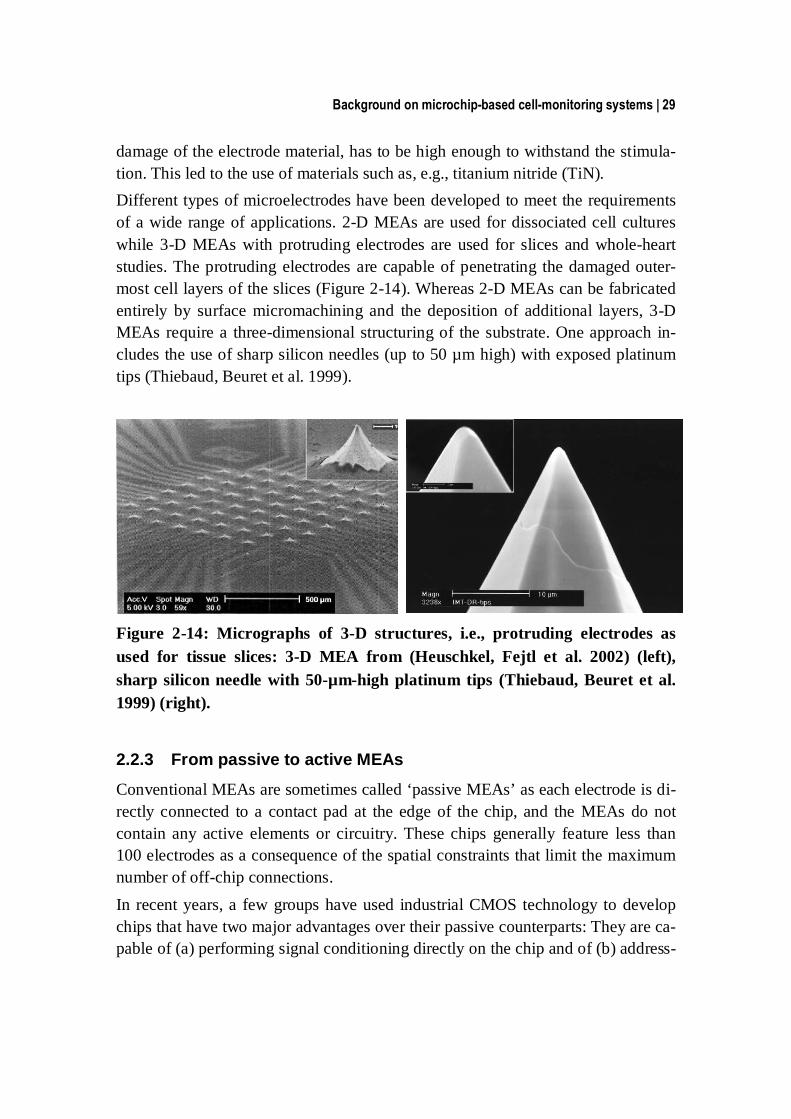
damage of the electrode material, has to be high enough to withstand the stimula-tion. This led to the use of materials such as, e.g., titanium nitride (TiN). Different types of microelectrodes have been developed to meet the requirements of a wide range of applications. 2-D MEAs are used for dissociated cell cultures while 3-D MEAs with protruding electrodes are used for slices and whole-heart studies. The protruding electrodes are capable of penetrating the damaged outer-most cell layers of the slices (Figure 2-14). Whereas 2-D MEAs can be fabricated entirely by surface micromachining and the deposition of additional layers, 3-D MEAs require a three-dimensional structuring of the substrate. One approach in-cludes the use of sharp silicon needles (up to 50 µm high) with exposed platinum tips (Thiebaud, Beuret et al. 1999).
Figure 2-14: Micrographs of 3-D structures, i.e., protruding electrodes as used for tissue slices: 3-D MEA from (Heuschkel, Fejtl et al. 2002) (left), sharp silicon needle with 50-µm-high platinum tips (Thiebaud, Beuret et al. 1999) (right).
2.2.3 From passive to active MEAs
Conventional MEAs are sometimes called ‘passive MEAs’ as each electrode is di-rectly connected to a contact pad at the edge of the chip, and the MEAs do not contain any active elements or circuitry. These chips generally feature less than 100 electrodes as a consequence of the spatial constraints that limit the maximum number of off-chip connections. In recent years, a few groups have used industrial CMOS technology to develop chips that have two major advantages over their passive counterparts: They are ca-pable of (a) performing signal conditioning directly on the chip and of (b) address-
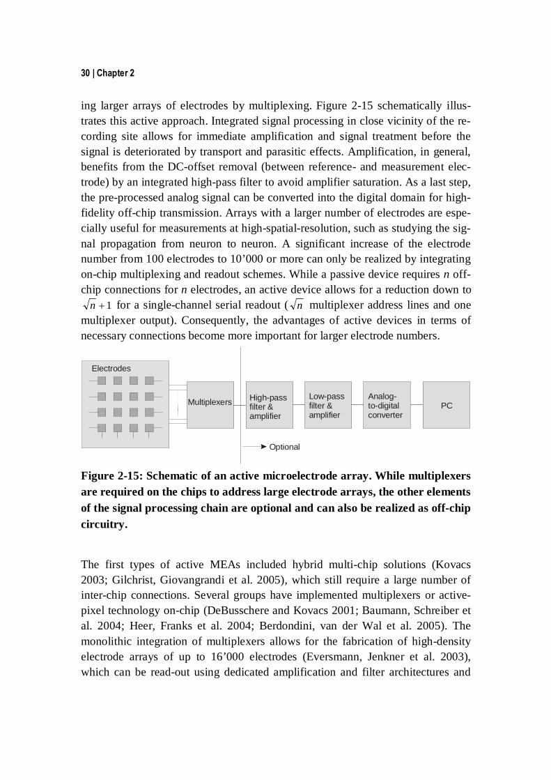
30 | Chapter 2
ing larger arrays of electrodes by multiplexing. Figure 2-15 schematically illus-trates this active approach. Integrated signal processing in close vicinity of the re-cording site allows for immediate amplification and signal treatment before the signal is deteriorated by transport and parasitic effects. Amplification, in general, benefits from the DC-offset removal (between reference- and measurement elec-trode) by an integrated high-pass filter to avoid amplifier saturation. As a last step, the pre-processed analog signal can be converted into the digital domain for high-fidelity off-chip transmission. Arrays with a larger number of electrodes are espe-cially useful for measurements at high-spatial-resolution, such as studying the sig-nal propagation from neuron to neuron. A significant increase of the electrode number from 100 electrodes to 10’000 or more can only be realized by integrating on-chip multiplexing and readout schemes. While a passive device requires n off-chip connections for n electrodes, an active device allows for a reduction down to
1n for a single-channel serial readout ( n multiplexer address lines and one multiplexer output). Consequently, the advantages of active devices in terms of necessary connections become more important for larger electrode numbers.
Electrodes
Multiplexers High-passfilter & amplifier
Low-passfilter &lifier
Analog-to-digital converter
Optional
PC
Figure 2-15: Schematic of an active microelectrode array. While multiplexers are required on the chips to address large electrode arrays, the other elements of the signal processing chain are optional and can also be realized as off-chip circuitry.
The first types of active MEAs included hybrid multi-chip solutions (Kovacs 2003; Gilchrist, Giovangrandi et al. 2005), which still require a large number of inter-chip connections. Several groups have implemented multiplexers or active-pixel technology on-chip (DeBusschere and Kovacs 2001; Baumann, Schreiber et al. 2004; Heer, Franks et al. 2004; Berdondini, van der Wal et al. 2005). The monolithic integration of multiplexers allows for the fabrication of high-density electrode arrays of up to 16’000 electrodes (Eversmann, Jenkner et al. 2003), which can be read-out using dedicated amplification and filter architectures and

Background on microchip-based cell-monitoring systems | 31
fast analog-to-digital converters on or off chip. In addition, some of these groups have also implemented signal-conditioning modules on the chips that include, e.g., operational amplifiers and high-pass filters for offset reduction. The fabrication of these bio-electronic chips relies on commercially available microelectronics fabri-cation and processing sequences with post-process micromachining for the micro-electrode array. In the meantime, several companies offer passive micro-electrode-array chips with associated desktop instrumentation for amplification and filtering (Bionas; MCS; Panasonic). Bionas (Rostock, Germany) offers an active MEA comprising 58 elec-trodes for action-potential recording plus a variety of microsensors to assess cell adhesion and cell morphology, cellular oxygen consumption, and extracellular acidification in the culture medium.
2.2.4 Applications of MEAs
Microelectrode arrays are used to perform electrophysiological measurements in a non-invasive and parallel fashion, and allow for in vitro studies of electrogenic cells in a mostly intact cellular environment. The three main fields of interests are (a) basic research in cell biology and physiology, (b) drug screening and (c) bio-sensing to detect environmental pollutants and warfare agents. Basic research includes investigating the potential for ion-channel screening of physiological processes like cellular excitation. Other applications are studying the synaptic plasticity (paired-pulse facilitation, long-term potentiation and long-term depression). Drug screening allows predictions about pharmacological and cytotoxic properties of potential new drugs. Since 2002, the Food and Drug Administration (FDA) and the European Agency for the Evaluation of Medicinal Products (EMEA) require cell-based testing of new drugs prior to human validation for assessing, e.g., the risk for delayed ventricular repolarization by monitoring the QT prolongation. Cardiomyocyte or whole-heart studies can be performed to detect these potential side effects of substances in the drug-development process. By measuring the field potential of the tissue, QT-interval prolongation can be detected, which might cause arrhythmia (and even death) in a patient receiving such a drug. Therefore safety validation for human pharmaceuticals may include in vitro assays (ICH) in the near future. In addition to recording the QT prolongation of heart-muscle cells, questions regarding atrial fibrillation, rhythmic/arrhythmic behavior and the veloc-ity of signal conduction and propagation can also be investigated (MCS) .
32 | Chapter 2
Living cells can also be used for environmental biosensing applications as they inherently react to a vast number of bio-hazardous substances. For this purpose, a portable system based on CMOS chips has been presented aimed at toxin detection and environmental monitoring (DeBusschere and Kovacs 2001). For the applications mentioned above, three different classes of specimens are used: Dissociated cell cultures from, e.g., neurons or heart-muscle cells that can be
kept for up to several weeks or months. Acute tissue cultures that are directly recorded from after preparation (hippo-
campus, cortex, spinal cord of adult animals). Organotypic tissue cultures from, e.g., the hippocampus, cortex, or spinal cord
of neonatal animals. The main synaptic characteristics and functions in the slices are preserved after the preparation as is the case for acute tissue slices, too. The advantage is that organotypic tissue cultures can be observed over a longer period (several weeks or months), while acute tissue cultures are usually discarded after the experiments.
Background on microchip-based cell-monitoring systems | 33
2.3 Interface between cell and chip
2.3.1 Biological aspects
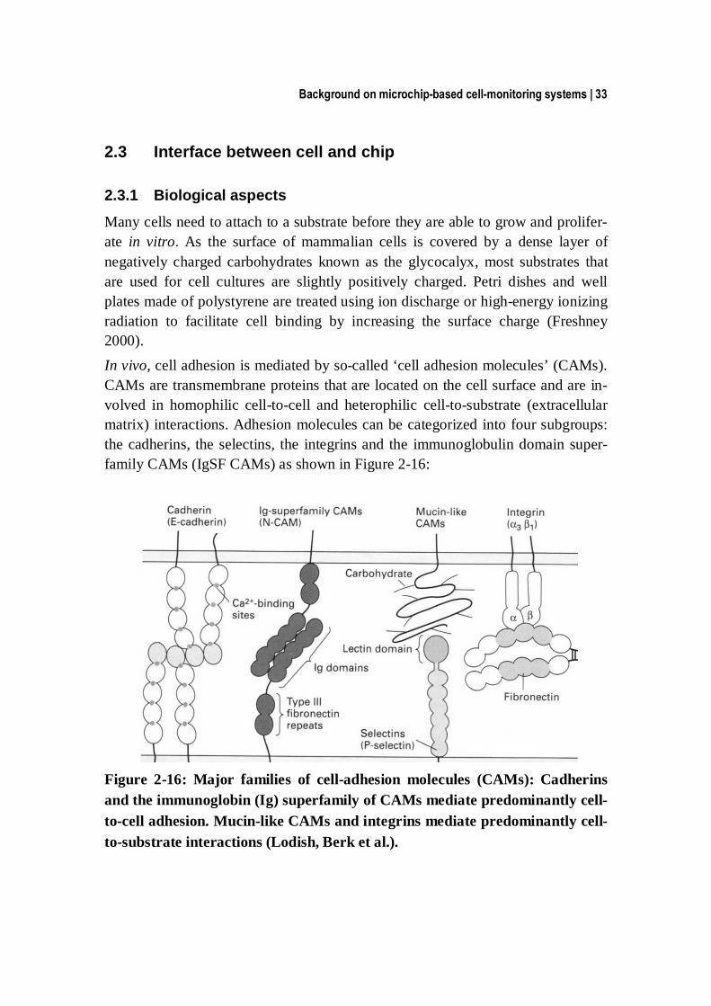
Many cells need to attach to a substrate before they are able to grow and prolifer-ate in vitro. As the surface of mammalian cells is covered by a dense layer of negatively charged carbohydrates known as the glycocalyx, most substrates that are used for cell cultures are slightly positively charged. Petri dishes and well plates made of polystyrene are treated using ion discharge or high-energy ionizing radiation to facilitate cell binding by increasing the surface charge (Freshney 2000). In vivo, cell adhesion is mediated by so-called ‘cell adhesion molecules’ (CAMs). CAMs are transmembrane proteins that are located on the cell surface and are in-volved in homophilic cell-to-cell and heterophilic cell-to-substrate (extracellular matrix) interactions. Adhesion molecules can be categorized into four subgroups: the cadherins, the selectins, the integrins and the immunoglobulin domain super-family CAMs (IgSF CAMs) as shown in Figure 2-16:
Figure 2-16: Major families of cell-adhesion molecules (CAMs): Cadherins and the immunoglobin (Ig) superfamily of CAMs mediate predominantly cell-to-cell adhesion. Mucin-like CAMs and integrins mediate predominantly cell-to-substrate interactions (Lodish, Berk et al.).

34 | Chapter 2
Cadherins are responsible for Ca2+-dependent cell-to-cell adhesion in verte-brate tissues (Alberts, Johnson et al. 2002).
Selectins are cell-surface carbohydrate-binding proteins (lectins) that mediate a variety of transient cell-to-cell adhesion interactions, e.g., in the bloodstream (Alberts, Johnson et al. 2002).
IgSF CAMs (immunoglobulin superfamily) are mainly responsible for Ca2+-independent cell-to-cell adhesion. These proteins contain one or more Ig-like domains that were characterized in antibody molecules. One of the best-studied examples is the neural cell adhesion molecule (N-CAM, Figure 2-16), which is expressed by a variety of cell types, including most nerve cells. N-CAM is one of the prevalent cell-to-cell adhesion molecules in vertebrates (Alberts, John-son et al. 2002). Additionally, some Ig-like cell-to-cell adhesion molecules bind to integrins such as the cell adhesion molecule L1 that binds to αvβ3 and α5β1 integrins. This interaction will be illustrated later in Chapter 4.
Integrins are a family of transmembrane glycoproteins that establish a direct connection between the extracellular matrix and the intracellular cytoskeleton. An integrin molecule is composed of two non-covalently associated transmem-brane subunits called α and β (Figure 2-17). In humans, there are at least 9 α subunits and 24 β subunits, which can form a variety of integrin receptors, pro-viding thereby different binding sites to the extracellular matrix (ECM). Once bound to the ECM, a whole cascade of reactions is triggered within the cell that causes the cytoskeleton to rearrange around such a contact. If several integrins simultaneously form connections, they enable the formation of larger contact areas also known as focal contacts (in 2D and 3D) (Cukierman, Pankov et al. 2002).

Background on microchip-based cell-monitoring systems | 35
Figure 2-17: The integrin is a transmem-brane heterodimeric protein composed of an α- and a β-subunit. Its extracellular domains bind to components of the ex-tracellular matrix, while the cytoplasmic tail of the β-subunit binds to actin fila-ments via several intracellular anchor pro-teins (Lodish, Berk et al. 2002).
Each integrin heterodimer may interact with one or more ligands that are usually ECM compounds (e.g. collagen, fibronectin, laminins) or are transmembrane pro-teins of the Ig-like superfamily (e.g. L1) expressed by surrounding cells (Previtali, Feltri et al. 2001). Table 1 gives a survey over studied integrin heterodimers and their ligands (limited to proteins such as collagen, fibronectin, laminins and L1). β1 β2 β3 β4 β5 β6 β7 β8 α1 Co, Lm - - - - - - - α2 Co, Lm - - - - - - - α3 Co, Lm, Fn - - - - - - - α4 Fn - - - - - Fn - α5 Fn, L1 - - - - - - - α6 Lm - - Lm - - - - α7 Lm - - - - - - - α8 Fn - - - - - - - α9 - - - - - - - - αv Co, Fn - Fn, L1 - Fn Fn - Fn Table 1: Integrin heterodimers and their ligands (Abbreviations: Co: colla-gen; Lm: laminins; Fn: fibronectin; L1: cell adhesion molecule L1; adapted and modified from (Previtali, Feltri et al. 2001)).
36 | Chapter 2
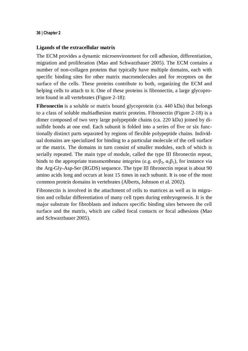
Ligands of the extracellular matrix The ECM provides a dynamic microenvironment for cell adhesion, differentiation, migration and proliferation (Mao and Schwarzbauer 2005). The ECM contains a number of non-collagen proteins that typically have multiple domains, each with specific binding sites for other matrix macromolecules and for receptors on the surface of the cells. These proteins contribute to both, organizing the ECM and helping cells to attach to it. One of these proteins is fibronectin, a large glycopro-tein found in all vertebrates (Figure 2-18): Fibronectin is a soluble or matrix bound glycoprotein (ca. 440 kDa) that belongs to a class of soluble multiadhesion matrix proteins. Fibronectin (Figure 2-18) is a dimer composed of two very large polypeptide chains (ca. 220 kDa) joined by di-sulfide bonds at one end. Each subunit is folded into a series of five or six func-tionally distinct parts separated by regions of flexible polypeptide chains. Individ-ual domains are specialized for binding to a particular molecule of the cell surface or the matrix. The domains in turn consist of smaller modules, each of which is serially repeated. The main type of module, called the type III fibronectin repeat, binds to the appropriate transmembrane integrins (e.g. αvβ3, α5β1), for instance via the Arg-Gly-Asp-Ser (RGDS) sequence. The type III fibronectin repeat is about 90 amino acids long and occurs at least 15 times in each subunit. It is one of the most common protein domains in vertebrates (Alberts, Johnson et al. 2002). Fibronectin is involved in the attachment of cells to matrices as well as in migra-tion and cellular differentiation of many cell types during embryogenesis. It is the major substrate for fibroblasts and induces specific binding sites between the cell surface and the matrix, which are called focal contacts or focal adhesions (Mao and Schwarzbauer 2005).

Background on microchip-based cell-monitoring systems | 37
Figure 2-18: The structure of a fibronectin dimer: The two polypeptide chains are similar but generally not identical. They are joined by two disulfide bonds near the C-termini. Each chain is almost 2500 amino acids long and is folded into five or six domains connected by flexible polypeptide segments. The three-dimensional structure of two type III fibronectin repeats was deter-mined by X-ray crystallography. The type III repeat is the main repeating module in fibronectin. Both the Arg-Gly-Asp (RGD) and the "synergy" se-quences are part of the major cell-binding site (adapted and modified from (Alberts, Johnson et al. 2002)).
Another important ECM ligand belongs to the laminin family: Laminins belong to the family of heterotrimeric glycoproteins abundant in base-ment membranes. Each laminin molecule is composed of three long polypeptide chains, α, β and γ; each of them is more than 1500 amino acids long and their combination produces more than 15 isoforms that have been described so far (Brandenberger and Chiquet 1995; Suzuki, F. et al. 2005). Five types of α chains, three types of β chains, and three types of γ chains are known; in principle, they can be assembled in a large family of 45 laminin isoforms. Laminin-1 (classic laminin) was isolated from the murine Engelbreth-Holm-Swarm (EHS) tumor. Its α1 chain (400 kD), β1- and γ1 chains, 220 kD each, are arranged in the shape of an asymmetric cross that is held together by coiled-coil and disulfide bonds (Figure 2-19). In vitro studies have shown that laminins can modulate the cell shape, proliferation, differentiation, cell migration and neuronal
α5β1
synergy site
α5β1
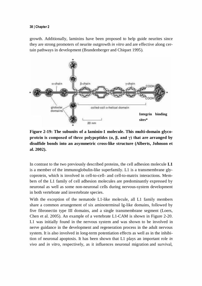
38 | Chapter 2
growth. Additionally, laminins have been proposed to help guide neurites since they are strong promoters of neurite outgrowth in vitro and are effective along cer-tain pathways in development (Brandenberger and Chiquet 1995).
Figure 2-19: The subunits of a laminin-1 molecule. This multi-domain glyco-protein is composed of three polypeptides (α, β, and γ) that are arranged by disulfide bonds into an asymmetric cross-like structure (Alberts, Johnson et al. 2002).
In contrast to the two previously described proteins, the cell adhesion molecule L1 is a member of the immunoglobulin-like superfamily. L1 is a transmembrane gly-coprotein, which is involved in cell-to-cell- and cell-to-matrix interactions. Mem-bers of the L1 family of cell adhesion molecules are predominantly expressed by neuronal as well as some non-neuronal cells during nervous-system development in both vertebrate and invertebrate species. With the exception of the nematode L1-like molecule, all L1 family members share a common arrangement of six aminoterminal Ig-like domains, followed by five fibronectin type III domains, and a single transmembrane segment (Loers, Chen et al. 2005). An example of a vertebrate L1-CAM is shown in Figure 2-20. L1 was initially found in the nervous system and was shown to be involved in nerve guidance in the development and regeneration process in the adult nervous system. It is also involved in long-term potentiation effects as well as in the inhibi-tion of neuronal apoptosis. It has been shown that L1 plays an important role in vivo and in vitro, respectively, as it influences neuronal migration and survival,
Integrin binding sites*
*
*
*
*

Background on microchip-based cell-monitoring systems | 39
neurite extension and fasciculation, axon guidance, regeneration, and synaptic plasticity (Schachner 1989; Hortsch, O'Shea et al. 1998).
Plasmamembrane Neuron specific
RSLE-encoding exon
Ankyrin binding site
Integrin bindingRGD motif
necessary forhuman L1-CAMhomophilic binding
N
1
2
3
4
5
6
C
L1Ig6 αvβ
3 integrin
Figure 2-20: Vertebrate L1-CAMs: the L1-type protein contains 6 Ig-like domains at their aminotermi-nus, indicated by pie-shaped sym-bols, which are followed by 5 fi-bronectin type III domains, repre-sented by striped rectangles and a single transmembrane segment (adapted and modified from (Hortsch 2000)).
In Chapter 4, the sixth immunoglobulin-like domain of the cell adhesion molecule L1 (L1Ig6) was used to study the molecular interface between cells and different material surfaces. L1Ig6 is used as a specific ligand for αvβ3 integrins expressed

40 | Chapter 2
on dorsal root ganglion neurons and on embryonic Schwann cells (Pittier, Sauthier et al. 2005). The L1Ig6 molecule is a comparably small molecule with a molecular weight of 8-10 kDa (Figure 2-20). While the proteins mentioned above provide bio-recognition-based cell adhesion, it is also possible to use unspecific electrostatic interactions to facilitate cell adhe-sion. One of the proteins capable of facilitating electrostatic cell adhesion is poly-L-lysine: Poly-L-lysine (PLL) is a polycationic polyamino acid that belongs to the polye-lectrolytes. It is positively charged under physiological conditions and promotes cell attachment by electrostatic binding. For the studies presented in this thesis, the outgrowth of DRG neurons on several adhesion proteins has been evaluated. Fibronectin and laminin-1 were selected from the group of extracellular matrix proteins. They were compared to L1Ig6 as a transmembrane protein and to PLL as a representative of the group of electrostatic cell-binding proteins. Further details of the interface between cells and substrates are given in Chapter 4.

Background on microchip-based cell-monitoring systems | 41
2.3.2 Electrical aspects
For extracellular measurements of the action potential of electrogenic cells, the in-terface between the electrode, the electrolyte (or medium) and the cell has to be well understood. Several parameters have to be taken into account: the impedance of the electrode (transducer), the electrode/electrolyte interface, the impedance of the protein layer, which binds to cells on the electrode surface and the cell mem-brane. Electrode-electrolyte interface When a metal electrode is placed into an electrolyte, chemical reactions may occur during which electrons are transferred between the electrode and the electrolyte resulting in the formation of a space-charge layer near the electrode. An electric field is generated, and water molecules are oriented at the electrode surface. This hydration sheath is called the inner Helmholtz plane. A layer of oppositely charged counter ions form the outer Helmholtz plane. This double layer of charge behaves like a parallel plate capacitor, the capacitance of which is given by
(1) dACH with ε as the permittivity of the electrolyte, A as the
electrode area and d as the distance between the both Helmholtz planes.
Equation (1) shows that the Helmholtz capacitance can be mainly influenced by the electrode area as the permittivity and the plate distance are defined by the elec-trolyte nature. This ideal capacitive behavior has been shown with liquid mercury systems, which have perfectly smooth surfaces. Most setups though use solid metal electrodes, where surface-roughness effects and specific adsorption lead to a frequency-depending constant-phase-angle element with an impedance ZCPA, which can be measured using impedance spectroscopy. This impedance is given by: (2) )( jwKZCPA with K as a measure of magnitude, and β as a constant
which has a value between 0 and 1 (typically around 0.8 for many electrode systems)
However, some leakage current across the double layer occurs due to electro-chemical reactions at the interface. This leakage current is included in the charge-transfer resistance, RCT, which can be derived from the Butler-Volmer equation for small applied voltages as:

42 | Chapter 2
(3) O
CT nFiRTR with R as the gas constant, T as the temperature, F as
the Faraday constant, n as the number of electrons involved in the electrode reaction, and io as the exchange-current density.
The latter one depends on the electrode material, the electrolyte composition and, therefore, on the resulting electrochemical reactions that occur when the electrode is placed in the electrolyte. The ions that are produced on the surface of the immersed electrode need to dif-fuse away to maintain an electrochemical equilibrium. This is modeled by the Warburg impedance ZW, a diffusion-limiting component which is strongly fre-quency dependent. At higher frequencies, the ions near the electrode surface are not able to follow the electric field anymore and the Warburg impedance tends to-wards zero. The electrical resistance from the measurement electrode to the counter electrode (often referred to also as the reference electrode) through the electrolyte is called the spreading resistance RS and varies depending on the coverage of electrodes by the cells. The spreading resistance depends only on the geometrical area and is for round electrodes given by
(4) l
RS 4ln
with δ as the specific solution resistance, and l as the diameter of the electrode area.
The equivalent-circuit model of the electrode-electrolyte interface can be derived from the parameters described above and is shown in Figure 2-21. Note that the diffusion impedance (Warburg) and the charge transfer at the double layer (RCT) are related to faradaic processes, which permit the flow of DC currents as com-pared to the non-faradaic double-layer capacitance CH (or ZCPA).
ZCPA
ZWElectrode ElectrolyteRCT
RS
Figure 2-21: Equivalent-circuit model of the electrode-electrolyte interface.

Background on microchip-based cell-monitoring systems | 43
For modeling the electrode-electrolyte interface, the following simplifications and assumptions from the equivalent-circuit model can be derived: Usually, the charge-transfer resistance, RCT (in the giga-ohm range), is consid-
erably larger than the Warburg impedance. Therefore, the latter one can be ne-glected in most cases.
At frequencies below 1 Hz, the charge-transfer resistance is the dominant fac-tor.
The constant-phase-angle element, ZCPA, leads to a decrease of nearly 20 dB/decade in the mid-frequency range.
At very high frequencies, the spreading resistance becomes the dominant ele-ment of the serial arrangement of ZCPA and RS.
A graph of the impedance of the electrode-electrolyte interface with the simplifica-tions explained above is shown in Figure 2-22. The spiking of neurons and car-diomyocytes is in the range of 150-5000 Hz.
| |Z
f [Hz]~1 Hz ~1 MHz
-20 dB/dec.
RCT
RS
Figure 2-22: Graph of the impedance of the electrode-electrolyte interface versus frequency using the simplified equivalent-circuit model.
Further details about the electrode-electrolyte interface are given, e.g., in (Morefield, Keefer et al.; Bard and Faulkner 2001). Impedance measurements of platinum microelectrodes carried out within the framework of this thesis will be described in Chapter 3.

44 | Chapter 2
Protein Layer Proteins are amino-acid chains that fold into unique 3-dimensional structures. The protein layer can be represented by a resistive element and a capacitive element in parallel. The values of these elements depend on the structure, the density and the molecular weight of the molecule.
Equivalent membrane model The selectively permeable cell membrane is a thin and structured bilayer of phospholipids and protein molecules that encloses the cell. Hodgkin and Huxley (Hodgkin and Huxley 1952) established an equivalent-circuit model of the cell membrane, as shown in Figure 2-23. In this model the major ionic currents through the cell membrane are described. Sodium and potassium currents through voltage-gated channels are represented by variable transmembrane conductances (gNa and gK). The leakage-ion current (remaining ions and charged species) is considered to be constant and is represented by the leakage conductance (gL). The electromotive forces as a consequence of the electrochemical potentials across the membrane are represented as voltage sources (ENa, EK, EL), and the cell membrane capacitance is represented by a capacitive element (Cm).
Outside
Inside
Cm3gNagKgL
EL EK ENa
Figure 2-23: Hodgkin-Huxley equivalent-circuit model representing the membrane of a neuronal cell.

Background on microchip-based cell-monitoring systems | 45
When the equivalent-circuit models of the electrode-electrolyte interface, the protein layer, and the cell membrane are combined, the following simplified model can be derived (Figure 2-24): the electrode- (in our case a platinum electrode) electrolyte interface can be represented by the Helmholtz capacitance (CH) parallel to the charge-transfer resistance (RCT). The adhesion protein (laminin-1, fibronectin or poly-L-lysine) is adsorbed onto the electrode. The impedance of the adhesion layer is represented by a resistive (RAD) and a capacitive element (CAD) in parallel. The resistance between the electrode and the bulk electrolyte due to a thin layer of medium between the cell and the electrode corresponds to the sealing resistance Rseal. In the case of pinholes in the protein layer or insufficient coverage of the electrode by the protein layer, some ions can bypass the adhesion layer and can diffuse directly to the electrode-electrolyte interface (Rsol, represented by the dashed line).
Electrode interface
Adhesion layer
Pt electrode
Vref
Vref
Zin
Rsol
CH RCT
CAD RAD
Rseal
Cm3g Na g K g L
ELEKENa Cell membrane
Figure 2-24: Model of the electrode-electrolyte interface and the adhesion layer and the cell membrane.

46 | Chapter 2
The goal of using equivalent-circuit models is to understand and to improve the electrode-cell interface. The impedance between the cell and the electrode surface should be as small as possible to ensure that most of the ions crossing the cell membrane have an impact on the transducer element. The majority of parameters of the cell membrane and the electrode-electrolyte interface are material proper-ties, which cannot be modified. The available parameters that can be varied are the Overall area of the electrodes Electrode material and morphology Selection of adhesion proteins (lower or higher molecular weight, concentra-
tion) The impedance of an electrode is inversely proportional to the electrode area (RCT, CH ~ δ l/A). Large overall electrode sizes feature a low charge-transfer resis-tance RCT and less thermal noise. Small electrode sizes in contrast allow for a bet-ter electrode coverage of the cell and, therefore, entail a higher sealing resistance. Furthermore, high-density electrode arrays can be fabricated for high-spatio-temporal-resolution imaging of the electrophysiological activity of electrogenic cell cultures. Generally, it seems appropriate to select an electrode area on the or-der of the cell diameter.

Perforated CMOS microchip | 47
3 Perforated CMOS microchip for immobilization and activity moni-toring of electrogenic cells
In this chapter, CMOS microelectronic chips are presented that were modified us-ing post-CMOS micromachining methods with the aim to enable precise place-ment of single cells in the center of the electrodes and to improve the cell-electrode coupling. Orifices were etched so that cell immobilization could be achieved by means of pneumatic anchoring; neonatal rat cardiomyocytes were placed on the arrays of perforated metal electrodes by applying a small underpres-sure from the backside of the chip. After four days of culturing, the cell electrical activity was measured, and the resulting signals were amplified by integrated on-chip circuitry, which comprises multiplexers to select electrodes for readout, an amplifier with selectable gain (2×, 10×, 100×) and a high-pass filter (100 Hz cut-off). The input-referred noise of the readout was below 15 µVrms (100 Hz - 4 kHz bandwidth). The micromachining methods, the bio-electronic chip itself, the electrical charac-terization of the circuitry, and the culturing methods are described in detail. The recordings of action potentials of neonatal rat cardiomyocytes after several days in vitro, which, on the one hand, were conventionally cultured (no pneumatic anchor-ing) and, on the other hand, were anchored and immobilized, are detailed and compared.
3.1 Introduction Over the past decade, microelectrode arrays (MEAs) have been widely used for parallel, non-invasive monitoring of electrogenic-cell activity (Thomas, Springer et al. 1972; Gross 1979; Pine 1980) as they constitute a powerful tool for long-time recording from cell cultures in, e.g., drug-screening applications. An over-view over the developments in this field and the corresponding literature is given in Section 2.2.2.

48 | Chapter 3
However, two issues generally limit the performance of these devices in a labora-tory environment: Passive MEAs generally feature less than 100 electrodes as a consequence of
the spatial constraints that limit the maximum number of off-chip connections. Due to the unpredictable distribution of cells on the chip surface during cell
seeding and subsequent cell development, a significant number of electrodes is only partially covered with cells, in particular in the case of low-density cul-tures.
The first aspect was successfully addressed by the advent of active MEAs with in-tegrated electronics, which are described in more detail in Section 2.2.3. However, reliable and good coverage of the electrodes with electrogenic cells is still nontriv-ial. Therefore, a variety of approaches to assure precise cell placement and good electrical cell-electrode coupling has been pursued. Precise placement of cells on electrodes is a pivotal issue as the extracellular signals are typically rather small, i.e., on the order of 10-100 µV for neurons and 500-1000 µV for cardiomyocytes. The probability to find a cell on an electrode can be easily increased by using high-density cultures. However, this is not in all cases desirable, in particular when the aim is to reveal cell-connectivity patterns or to investigate intercellular signal transfer: Low-density cultures allow for studying signal propagation pathways be-tween the cells upon stimulation. Without a cell-placement technique, low-density cultures will inevitably entail a low probability of cells sitting on the electrodes so that it is difficult to obtain relevant experimental data. The techniques that have been used to enhance the cell coverage of the electrodes can be classified into surface-chemical and physical methods. The first class uses adhesion-promoting mediators, which are often extracellular matrix molecules to promote cell adhesion. To achieve local immobilization of cells, the adhesion pro-teins need to be patterned or modified. Though most approaches have been devel-oped to facilitate neurite outgrowth in defined networks, in principle all these techniques can also be used to immobilize cells directly onto electrodes. The most common technique of patterning proteins is micro-contact printing, which entails the use of an elastomeric stamp to transfer the desired pattern onto the chip surface (Mrksich, Dike et al. 1997; Kane, Takayama et al. 1999; Scholl, Sprossler et al. 2000). Other efficient approaches include the direct patterning of proteins by pho-tolithography (Kleinfeld, Kahler et al. 1988; Sorribas, Padeste et al. 2002; Wyart, Ybert et al. 2002; Rohr, Fluckiger-Labrada et al. 2003), the photolithographic pat-terning of poly(ethyleneimine), PEI, by lift-off to achieve hydrophobic and hydro-philic regions for selective cell growth (Ruardij, Goedbloed et al. 2000), ink-jet

Perforated CMOS microchip | 49
printing (Turcu, Tratsk-Nitz et al. 2003; Sanjana and Fuller 2004), and mul-tiphoton crosslinking of proteins (Kaehr, Allen et al. 2004). To achieve high reso-lution and exact alignment of the protein patterns with regard to the underlying electrodes, self-assembled monolayers of proteins on, e.g., gold substrates were also used (Franks, Tosatti et al. 2004; Lussi, Michel et al. 2004). In addition to chemical patterning, physical structures that help to immobilize the electrogenic cells on the active electrode area can be implemented. They include photo-patterned Epon SU-8 (Merz and Fromherz 2002), polyimide (Zeck and Fromherz 2001), parylene (Meng, Tai et al. 2002), silicon-based (Maher, Dvorak-Carbone et al. 1999) or polyester (Merz and Fromherz 2005) pits or cages, which inhibit the migration of the cells. However, manual pipetting is needed to place the cells inside these structured barriers or cages, which renders the assembly of larger numbers of cells rather cumbersome. Alternatively, dielectrophoretic trapping of cells by a non-uniform electric field has been demonstrated to provide an efficient method to automatically place cells on electrodes (Heida, Rutten et al. 2001; Manaresi, Romani et al. 2003; Gray, Tan et al. 2004). Dielectrophoretic trapping requires, however, a comparatively complex chip structure and electronic setup. Physical forces, such a suction, have been shown to allow precise positioning of cells onto planar, passive substrates with much lower efforts (Thielecke, Stieglitz et al. 1999). In this chapter, a novel chip design is described, which combines on-chip microe-lectronics, specifically CMOS circuitry, with micromachined features to achieve both, active signal processing as well as effective cell placement by means of a physical immobilization method similar to the technique described by (Thielecke, Stieglitz et al. 1999). The chip was fabricated in a commercial 0.8-µm CMOS process and includes on-chip amplification and analog multiplexing units. The immobilization features, which are small holes, were fabricated on wafer level during the CMOS postprocessing, which is different from most approaches de-scribed above. The cells were immobilized by means of 3-µm-diameter, vertical, through-chip orifices in the center of the electrodes, through which a slight underpressure was applied from the backside of the chip. After all electrodes/orifices were occupied with cells, the pressure was released, and the cells remained at the electrodes and adhered to the chip surface during the culturing period of several days. This tech-nique, referred to as “pneumatic anchoring”, allows to reliably cover all elec-trodes, it does not require any individual manipulation of the cells and enables the cultivation of low-density cell populations for drug-screening applications and

50 | Chapter 3
others. The immobilization directly on the electrodes/orifices also improves the electrical coupling between the cells and the electrodes.
3.2 Device description The device is a 55 mm2 chip fabricated in standard industrial CMOS technology with subsequent dedicated micromachining steps to deposit the electrodes and to realize the immobilization features.
Figure 3-1: Device schematic showing the on-chip blocks: 16 electrodes, 4-to-1 multiplexers, 4 high-pass filters (HPF), and programmable-gain amplifiers. A four-channel adjustable low-pass filter (LPF) with further amplification with a low-noise amplifier (LNA) was realized externally.
3.2.1 CMOS circuitry
The cell area in the center of the chip includes an array of 4 by 4 platinum elec-trodes with a ring-shape reference electrode (Figure 3-1). Four independent cir-cuitry blocks for signal conditioning are provided to enable simultaneous read-out of four electrodes without switching of the multiplexers. The four electrodes of each quadrant are connected to four-to-one multiplexers at the input of each signal chain. One electrode per quadrant can be selected for recording at the same time. Each multiplexer feeds into a programmable-gain amplifier (gain 2, 10, and 100) that amplifies the extracellular signals (signal level approx. 10 to 1000 µV) coming from the electrodes. Before amplification, the signals are high-pass filtered (100 Hz cut-off) on-chip to prevent input saturation of the amplifiers as a conse-quence of DC potential differences between the reference and the measurement electrode. The signals are then transmitted off-chip and further amplified (gain 10, 100) and low-pass filtered (4 kHz tuneable cut-off) using external circuitry.

Perforated CMOS microchip | 51
Afterwards, the signals are translated into the digital domain using an analog-to-digital converter card (DAQ-card, National Instruments, Austin, Texas, USA).
3.2.2 Microelectrodes
The aluminum (metal layer 1 & 2) of the CMOS process cannot be used as an electrode material as it shows poor electrochemical stability in physiological solu-tion and as it is poisonous for most cell types. Therefore, metal contacts are only arranged along the edges of the chip, which are then electrically connected to the sputtered platinum metal electrodes (size: 20×20 µm2) in the cell area. The pat-terning of the required titanium/tungsten adhesion layer and the platinum layer is done during post-CMOS micromachining.
3.2.3 Cell-immobilization features
The diameter of the cell body of neonatal rat cardiomyocytes is in the range of 20 µm so that orifices with a small diameter have to be fabricated to prevent any suction of the cells through the chip. These orifices are generated by means of re-active-ion etching (RIE). Since the orifice diameter may be enlarged during a long dry-etching process, which would be needed to etch through the whole wafer, the silicon substrate underneath the electrode array is thinned from the backside. This procedure allows for perforating each electrode with a 3-µm-diameter orifice, which then can be used for pneumatic cell anchoring.
3.2.4 Packaging and setup
The chip is mounted on a perforated dual-in-line (DIL) ceramic package that en-ables to apply pressure from the chip backside; the bond wires are sealed using an epoxy, and a plexiglas ring is mounted to form a reservoir for the cell suspension. Cell placement and immobilization is achieved by applying a slight underpressure from the backside, which drags the cells towards the electrode centers. Measure-ments of the electrical activity of neonatal rat cardiomyocytes (NRCs) were per-formed after four days in vitro, on the one hand, with conventionally plated cells (no pneumatic anchoring) and, on the other hand, with immobilized cells.

52 | Chapter 3
3.3 Fabrication The chip including the microlectronic components was fabricated in a standard 0.8-µm CMOS double-poly, double-metal process as provided by austriamicrosys-tems. The post-CMOS micromachining and packaging was done in house, the dif-ferent steps of which are detailed below:
3.3.1 Step 1: orifice etching
3-µm orifices were etched by reactive-ion etching using front-side photolithogra-phy. The etching opened the field oxide and the inter-metal oxides (ca. 1.5 µm) of the CMOS process and etched 5 µm deep into the silicon. The wafer thinning and membrane formation was performed in a later stage in order not to create a rather fragile structure already at the beginning of the micromachining sequence.
3.3.2 Step 2: lift-off process
Titanium/tungsten (20 nm) as adhesion layer and platinum (200 nm) as the elec-trode material were sputtered onto the wafer and patterned using a lift-off process. To assure a high undercut profile of the resist for better lift-off characteristics, a bi-layer lift-off resist (LOR 7B, Microchem, Newton, Massachusetts, USA) was used. The first layer, LOR, is a UV-insensitive material that was spun onto the wa-fer. The next layer, a photoresist, Shipley 1828, was subsequently spun on the wa-fer and was exposed to UV light in the mask aligner. During development (Shipley FM 8022), the Shipley resist was removed, where it was exposed to light. The LOR was then isotropically etched and left an undercut. After sputtering, the metal lift-off was done in a remover bath (Microchem Remover 1165) (Figure 3-2).

Perforated CMOS microchip | 53
(a)
Silicon substrate
LORS1828
Platinum
(b)
(c)
Figure 3-2: (a) Lift-off process steps, (b) SEM picture illustrating the LOR undercut, (c) micrograph of platinum electrodes after lift-off.
3.3.3 Step 3: passivation
A 1-µm silicon-nitride passivation layer was deposited by PECVD and was opened at the measurement- and the reference-electrode sites by reactive-ion etch-ing.
3.3.4 Step 4: electro-chemical etching
The silicon underneath the electrode array was thinned to a 5-µm membrane by an anisotropic wet etching step from the backside of the wafer. Here, a 4-electrode electro-chemical etch-stop setup (AMMT, Germany) and 6-molar aqueous KOH solution at 90°C were used. During etching, the wafer was mounted in a wafer holder to protect the frontside of the wafer. The wafer holder was then immersed in the KOH solution. The n-wells of the CMOS wafer were maintained at the solu-tion potential, well above the passivation potential (-1.2 V). At the same time, the p-doped substrate was set to the open-circuit potential (-1.5 V) by the fourth elec-trode to assure the etching of the p-layer even in the presence of leakage currents (Figure 3-3). After the etching stops, an over-etching time of 15 min. was allowed to ensure complete passivation of the silicon membranes.
30 µm

54 | Chapter 3
Si
CounterElectrode
ReferenceElectrode
A A
Potentiostat
n p
0V
-1.5
V
Volta
ge v
s R
E(V)
150 160 170 180 190
0
2
4
6
8
10
Etc
hing
cur
rent
[mA
]
Time [min.]
Figure 3-3: Schematic of the ECE setup (left) and a typical etch-stop graph of an electrochemically etched CMOS wafer (right).
3.3.5 Packaging
Finally, the wafer was diced into single chips, and these were mounted on perfo-rated DIL packages using an intermediate poly(dimethylsiloxane) layer. The per-foration in the DIL package allowed for pressure application from the backside. After bonding, the bond-pads were sealed using an epoxy (Supreme 42HT-T, Mas-terbond, USA). These fabrication steps are summarized in Figure 3-4. Micrographs of the chip, the electrode area and the perforated electrodes are shown in Figure 3-5.

Perforated CMOS microchip | 55
Circuitry
CMOS chip
Circuitry
1. Step
2. Step
3. Step
4. Step
Figure 3-4: Illustration of the fabrication steps: 1. CMOS wafer after fab-out; 2. Reactive-ion etching of the orifices; 3. Patterning of the platinum meas-urement- and reference electrodes by lift-off, PECVD-nitride deposition and opening at the electrodes by RIE; 4. Anisotropic etching of silicon using a 4-electrode electro-chemical etch-stop technique.

56 | Chapter 3
30 µm300 µm
Figure 3-5: Micrograph of the micromachined chip (5×5 mm2, left), the elec-trode area (middle) and close-up of the perforated platinum electrodes (right).
3.4 Experimental
3.4.1 Cell culturing
Primary neonatal rat cardiomyocytes (NRCs) were taken from 3-day old rats and harvested as previously described by Auerbach et al. (Auerbach, Bantle et al. 1999). The cardiomyocytes were purified using gradient centrifugation and seeded in plating medium consisting of 68% Dulbecco's Modified Eagle Medium, DMEM (Amimed, BioConcept, Allschwil, Switzerland), 17% Medium M199 (Amimed), 10% horse serum, 5% fetal calf serum (both Life Technologies, Gaithersburg, USA), 4 mM glutamine, and 1% penicillin-streptomycin (both Amimed). After 24 hours, the plating medium was exchanged for a maintenance medium, consist-ing of 78% DMEM, 20% medium M1999 (both Amimed), 1% horse serum (Life Technologies), 1% penicillin-streptomycin and 4 mM glutamine (both Amimed). The plating medium features a higher serum content for better adhesion to the sur-face of the bio-electronic chip. The NRCs were kindly provided by Evelyne Perriard from the Institute of cell bi-ology, ETH Zurich.
3.4.2 Chip preparation
The chips were sterilized in 70% ethanol, before drying under UV light for 30 min. The surface was then coated with the adhesion protein laminin-1 (20 µg/mL in phosphate-buffered saline solution (PBS), Sigma Aldrich) and incu-

Perforated CMOS microchip | 57
bated at 37°C, 5% CO2 for two hours. Afterwards, the chips were washed twice with PBS before cell placement.
3.4.3 Cell placement
For pneumatic anchoring, an underpressure of ~20 kPa below ambient pressure was applied for a few seconds from the backside of the chip until all electrodes were occupied with cells. Owing to the adhesion layer, the cells adhered spontane-ously to the electrode surface and remained on the electrodes even without con-tinuously applying underpressure. The chips were then incubated for 4 days at 37°C, 5% CO2, and the medium was replaced with maintenance medium after one day in culture. Afterwards, the medium was changed every two days. Beating of the cardiomyocytes on top of the electrodes could be observed already after one day in vitro. The overall morphology of immobilized cardiomyocytes in a low-density culture is shown in Figure 3-6 (a) using light microscopy. All electrodes are occupied by cells or small clusters of cells. Such cell clusters were probably the result of incomplete cell separation during the trypsinization step. Figure 3-6 (b) shows an immunostaining of the immobilized cardiomyocytes after 4 days in culture, using an anti-sarcomeric-α-actinin antibody (sarcomeric clone EA-53, SigmaAldrich) and a selective fluorophore to visualize the z-disks. The round black spot in the staining picture represents the orifice. Our immobilization tech-nique can be considered to be gentle enough as the cells on orifices show an intact morphology of the z-disks indicating that the cells on the holes remained intact.

58 | Chapter 3
(a) (b)
Figure 3-6: Micrographs showing (a) immobilized NRCs on the orifices and (b) stained NRCs after 4 days in vitro. The z-disks (grey spots) were visual-ized by staining the sarcomeric-α-actinin to show the intact morphology of the cells (scale bars 30 µm).
3.5 Results and discussion
3.5.1 Electrical characterization
The transfer function of the microchip and the associated, external electronics was electrically characterized using a network analyzer (HP 4195A). As Figure 3-7 shows, the amplifier (2×, 10×, 100×; 10× external gain) and filter performance meet the specifications mentioned above. The corner frequencies are defined by the on-chip high-pass filter (100 Hz) and the external low-pass filter (4 kHz).
orifice
z-disks of NRCs
electrode

Perforated CMOS microchip | 59
10 100 1000 10000 100000
-10
0
10
20
30
40
50
60
Gai
n [d
B]
Frequency [Hz] Figure 3-7: Bode magnitude plot of the amplification and filtering circuitry characteristics of the three programmable gain stages plus the external gain stage which was set to 10×.
To show the influence of the 3-to-5-µm orifices, impedance measurements of plain metal electrodes and of the perforated electrodes were performed. A sinusoidal test signal (100 mVpp) was introduced to a physiological solution via a platinum wire, which acted as the counter electrode. The resulting current recorded by the micro-electrodes was measured using a current-to-voltage converter connected to a dy-namic signal analyzer (HP 3562A). The slope of the measured impedance in Figure 3-8 can be explained by the fact that at frequencies below 1 Hz, the high charge–transfer resistance, RCT, is dominant, while in the mid-frequency range, the interface capacitance leads to a decrease of the impedance of -20 dB per decade (Franks, Schenker et al. 2005). In this range, the impedance of the perforated elec-trodes is about 1.4 times higher than that of plain platinum electrodes of the same size. This is mainly the result of the smaller area of the perforated electrodes that leads to a lower interface capacitance. The input-referred noise of the chip is below 15 µVrms within the filter bandwidth (100 Hz – 4 kHz) for the plain and the perforated electrodes, respectively.
1000× 100× 20×

60 | Chapter 3
0.1 1 10 100 1000 10000 100000104
105
106
107
108
109
Impe
danc
e [O
hm]
Frequency [Hz] Figure 3-8: Impedance measurements of the platinum electrodes with and without orifices (without circuitry); the dotted line shows the magnitude of the impedance of the plain electrodes, the solid line shows an approximately 1.4× larger impedance for the electrodes with orifices.
Table 1 summarizes the main features of the bio-electronic chip:
Technology 0.8-µm double-poly double-metal CMOS process and post-CMOS micromachining
Chip size 5×5 mm2
Number & size of electrodes 16 electrodes; 20×20 µm2
Gain (on-chip) 2×, 10×, 100×
Gain (off-chip) 10×, 100×
Power dissipation 9 mW at 5 V
Input-referred noise 15 µVrms; 100 Hz – 4 kHz Table 1: Features of the bio-electronic chip.
··· plain electrodes — perforated electrodes

Perforated CMOS microchip | 61
3.5.2 Cell recordings
Electrogenic signals of on-chip-cultured neonatal rat cardiomyocytes (NRCs) were recorded to assess the chip and system performance. Recordings from convention-ally plated cells on plain electrodes were compared to those from pneumatically anchored low-density cultures, each after four days in vitro. These measurements evidence the possibility to acquire electrical signals from all electrodes even in low-density cell cultures by applying the pneumatic-anchoring technique. Before conducting the electrical measurements, phenylephrine (100 µM end con-centration) was added to the culture of the conventionally plated cells to induce spontaneous beating and to enhance the beating intensity and frequency of the NRCs. Two hours after the drug dosing, the extracellularly measured potential of the confluent layer of NRCs was about 500 µV and a regular beating at a rate of approximately 5 beats per second was observed as shown in Figure 3-9. Also, three simultaneously recorded electrodes show almost identical signals as a conse-quence of the confluent layer of NRCs covering the whole active electrode area. The spontaneous activity is usually triggered by a pacemaker region in the culture and then spreads through the whole culture owing to the tight interconnection and fast signal transmission of the cardiomyocytes in a confluent layer. Each electrode underneath such a confluent layer records a so-called “field potential”, which originates from a larger patch of cells that show synchronized activity. Therefore, the signal intensities are usually rather high.

62 | Chapter 3
Figure 3-9: Cell recording of conventionally plated neonatal rat cardiomyo-cytes after 4 days in vitro; the measurements show a constant beating of the monolayer every 0.2 sec and a signal amplitude of approximately 500 µV.

Perforated CMOS microchip | 63
However, the recordings from the anchored cells or clusters in the low-density cul-tures showed significantly different characteristics: The signal intensities and beat-ing patterns of different electrodes were, if ever, only weakly correlated as shown in Figure 3-10. This can be explained by the fact that clusters of cardiomyocytes were formed around each electrode, but that there was no physical connection be-tween the individual cell clusters, e.g., by protein channels, so called “connexins”, that allow for passage of ions from one cell to the other. Only such physical con-nection can lead to synchronizing the cell beating over the whole recording area. Note, that in the experiments with the perforated electrodes, no phenylephrine was added before the measurements, so that the beating frequency in the recorded sig-nals may be lower in comparison to the experiments with the confluent layer. The most important goal of this experiment, the full coverage of all electrodes, could be repeatedly achieved as shown exemplarily in Figure 3-6 (a). In some cases, one cell was immobilized on an electrode, while in other cases, a cluster of NRCs was formed around the electrode. These clusters originate, often, from in-complete cell dissociation during the cell harvesting. Without the holes and the underpressure application it would be unlikely to have cells or cell clusters on all the electrodes. In an additional step the non-immobilized cells can also be washed away by applying a shear flow, which has not been done here. In all experiments electrical recordings from the anchored NRCs could be obtained, though the elec-trical signals from the anchored cells/clusters may show a slightly higher noise level than the measurements of the cells using non-perforated electrodes, which was, most probably, due the higher impedance of the perforated electrodes. In a future design, the overall area of the perforated electrodes will be increased to compensate for the perforation loss. The other important issue besides the elec-trode area and impedance is the seal between electrode and cell. The better the sealing, the larger the recorded signal. The magnitude of the signals of the cells and clusters on the perforated electrodes was similar to those of the field potentials of the confluent layer. One reason for that could be the fact that the pneumatic an-choring helps to precisely place the cell on the electrode and improves the cell-to-electrode sealing. This will be investigated in more detail in the future.

64 | Chapter 3
Figure 3-10: Cell recording of pneumatically anchored cells; the cell clusters around each electrode show an independent beating cycle. Although no phenylephrine was added beforehand, the signal strength was sufficient to be recorded.

Perforated CMOS microchip | 65
3.6 Conclusion The CMOS microchip platform with integrated microelectrode array and pneu-matic anchoring is a versatile and efficient instrument for parallel, extracellular monitoring of cell activity. By combining microelectronic circuitry with micro-machined features, a powerful placement technique and an efficient signal precon-ditioning and multiplexing were realized, which will enable the fabrication of much larger arrays in the future. Reliable cell placement with coverage of all elec-trodes even in low-density cultures while fully retaining the cell viability and ac-tivity was demonstrated. Signal recordings were obtained from conventionally plated and pneumatically anchored neonatal rat cardiomyocytes with good signal-to-noise ratio. The concept of pneumatic anchoring can be advantageous for a wide variety of applications ranging from low-to high-density cultures and from cardiomyocytes to neurons. For instance, the study of signal transmission in neuronal networks would benefit from the precise placement of the cells and the coverage of all elec-trodes. A different application is highly parallel drug screening as the system al-lows for recording the signals of individual cells or cell clusters not influenced by the neighbouring cells.


Molecular design of the neuron-to-CMOS interface | 67
4 Molecular design of the neuron-to-CMOS interface
This chapter describes experiments on differently modified CMOS surfaces using chicken dorsal root ganglia. Neurite outgrowth has been evaluated on different ad-hesion-promoting protein layers adsorbed on CMOS substrate materials. For this purpose, silicon chips were coated with silicon nitride, platinum or gold, and four different protein layers were adsorbed: laminin-1, L1Ig6, fibronectin, or a combi-nation of poly-L-lysine and laminin-1. Scanning-electron microscopy and transmission-electron microscopy were per-formed to further analyze and characterize the cell-to-electrode interface.
4.1 Introduction There is a growing interest in the investigation of the electrophysiological activity of electrogenic cell cultures using extracellular recording techniques. Microelec-trode arrays (MEAs) can be used to obtain a better insight into the properties and functions of neuronal networks. One prominent advantage of MEAs is based on the fact that the cells can be cultured on these devices for several weeks or months. Thus, frequent and long-term recordings can be performed without damaging the cells through the measurement system. Comparable long-term studies are impossi-ble with invasive techniques such as patch-clamp. Despite many advantages, the use of MEAs still poses technical challenges. To ob-tain measurements with high signal-to-noise ratio, the signal-recording setup or the read-out circuitry needs to be of high performance. Also, the compatibility be-tween the MEA substrate, the adhesion-promoting protein layer and the cells has to be optimized. The requirements concerning this second aspect are stringent: good adsorption of the adhesion proteins on the CMOS surfaces, adhesion and proliferation of cells on these layers and the potential of long-term culturing. The protein layer also plays an important role for the electrical signal transmission as it constitutes the interface between the cell and the electrode. As a consequence, the

68 | Chapter 4
protein/substrate interface should not only be optimized for biocompatibility, but also for good electrical coupling between the cell and the electrode surface as the amplitude of the extracellular signal is minute (approximately 10-1000 µV). Moreover, the distance between the cell and the electrode surface should be as small as possible to assure good electrical coupling, and the cell adhesion should be strong to provide a high sealing resistance. In previous studies a wide variety of different combinations of cells, adhesion-protein layers and chip material surfaces has been used to culture different types of neurons on bio-electronic chips. However, systematic studies to investigate the in-fluence of different adhesion proteins and material surfaces on the cell growth on microchips have not been published yet. Table 2 gives a survey of the recently published literature: Author: Species: Age: Cell type: Adsorption
layer: (Berdondini, van der Wal et al. 2005)
rat neonatal ventricular car-diomyocytes
collagen (human placenta type VI)
(Sprossler, Richter et al. 1998)
rat 3 days postnatal cardiomyocytes fibronectin (10 µg/ml)
(Chang, Brewer et al. 2000)
rat embryonic hippocampal neurons
poly-D-lysine (100 µg/ml)
(Potter and De-Marse 2001)
rat embryonic (E18)
cortical neurons 0.05% polyethyl-eneimine (PEI), then 1 mg/ml laminin
(Jimbo, Kawana et al. 2000)
rat neonatal (rat embryos E18)
cortical neurons laminin or poly-D-lysine
(Ruardij, Goed-bloed et al. 2000)
rat newborn (1 day old)
cerebral cortical neurons
PEI (10 µg/ml as adhesion layer) and fluorcarbon (non adhesive)
(Ruaro 2005) rat 3 days postnatal hippocampal neurons
polyornithine (50 µg/ml)
(Chiappalone, Vato et al. 2003)
chicken embryonic (E7-8)
spinal cord neu-rons
poly-L-lysine or laminin
(Morefield, mouse embryonic spinal cord & poly-L-lysine and

Molecular design of the neuron-to-CMOS interface | 69
Keefer et al. 2000) (Gross, Harsch et al. 1997)
cortical neurons laminin
(Bonifazi and Fromherz 2002) (Lambacher, Jenkner et al. 2004)
freshwa-ter snail Lymnaea stagnalis
poly-L-lysine (Sigma P6516)
(Hammerle, Egert et al. 1994)
chicken embryonic (E14-18)
retinal ganglion cells
poly-D-lysine (Boehringer, 500 µg/ml)
Table 2: Summary of species, cell types, age of the donor animal, and adsorp-tion layers used by several groups for long-term culturing. Concentrations are only listed if detailed in the corresponding paper.
Besides the cell-biological characterization, physical distance measurements be-tween the cell surface and the electrode were described for several typical adhe-sion proteins. Fluorescence interference contrast (FLIC) microscopy was intro-duced by Fromherz et al. to measure the distance between embryonic rat hippo-campus neurons or snail (Lymnae stagnalis) neurons and an oxidized silicon chip surface. The membranes of the neurons were visualized by an integrated fluores-cent dye, and the distance was assessed by interference patterns caused by stand-ing waves due to surface reflections. As the fluorescence intensity of the dye inte-grated into the cell membranes depends on the interference patterns due to the cleft between the cell and the silicon oxide surface, protein layer thicknesses of about 100 nm for laminin, 60 nm for fibronectin (Braun and Fromherz 1998) and 40 nm for poly-L-lysine were determined (Zeck and Fromherz 2003). In this chapter, measurements of neurite extension were performed to determine whether CMOS-surface materials treated with different adhesion proteins allowed for neuronal attachment and differentiation. Neurite extension can be regarded as a measure for neurite differentiation and precedes neuronal network formation. The intention of this study was to analyze different adhesion proteins that have been described to favor neurite extension. Laminin is widely used, as it specifically ad-dresses integrins in the neuronal cell surface (Previtali, Feltri et al. 2001; Clegg, Wingerd et al. 2003; Previtali, Nodari et al. 2003). Fibronectin is an important substrate for fibroblasts and induces specific binding sites between the cell surface

70 | Chapter 4
and the matrix, called focal contacts or focal adhesions (Mao and Schwarzbauer 2005). L1Ig6 is used as a specific ligand for αvβ3 integrins expressed on dorsal root ganglion neurons and Schwann cells (Pittier, Sauthier et al. 2005). This mole-cule is considerably smaller with a molecular weight of 8-10 kDa as compared to laminin (800 kDa) and fibronectin (440 kDa). Poly-L-lysine is a polycationic amino acid and promotes cell adhesion by electrostatic forces. The idea was to ex-amine whether the cleft between the neurons and the chip surface can be mini-mized by using a thin adhesion protein layer. All further studies aimed at investi-gating if the adhesive layers allow for neurite extension, which is a prerequisite for neuronal network formation. Neurite outgrowth was analyzed on silicon nitride, platinum and gold surfaces af-ter adsorption of the different adhesion proteins. These substrates were selected since they represent typical CMOS-passivation and post-CMOS metal layers. CMOS technology was of primary interest for this study, because active circuitry such as multiplexers, amplification stages and filters can be integrated, enabling thereby the fabrication of MEAs with large electrode arrays for highly parallel re-cordings (Eversmann, Jenkner et al. 2003; Heer, Franks et al. 2004). Peripheral dorsal root ganglion neurons from embryonic chicken were cultured for several days on these different surface layers to study (a) the neurite outgrowth and (b) the cell-to-surface distance. The neurite outgrowth was investigated by culturing the neurons for two days on the different adhesion protein/substrate combinations, and by evaluating the neurite length after staining with specific an-tibodies against axonal proteins. Single DRG neurons were furthermore cultured for up to one week to investigate the network characteristics. The interface between cultured neurons and platinum-covered chips was further analyzed by scanning electron microscopy (SEM) and by transmission electron microscopy (TEM).
4.2 Experimental All studies were performed with chicken dorsal root ganglia (DRG). The main rea-sons include the relatively simple harvesting procedure of the cells, the exactly de-fined stage of the embryonic development and the spontaneous neurite outgrowth from explanted ganglia (Banker and Goslin 1998). These arguments render those DRGs an ideal system to study the behavior of growing neurites.

Molecular design of the neuron-to-CMOS interface | 71
A commercial 0.8 µm-CMOS process as provided by austriamicrosytems (AMS) was used to fabricate the test chips. The dielectric layers of the chips were defined by the CMOS process and consisted of either silicon oxide or silicon nitride. As the last passivation step was the evaporation of a 1000-nm-thick PECVD (plasma-enhanced chemical vapor deposition) silicon-nitride layer, the determination of the neurite extension was performed on silicon nitride The patterning of the electrodes was done in a post-CMOS process. It should be noted that the aluminum layers, metal 1 and 2 of the CMOS process, cannot be used as electrodes since aluminum is not chemically inert and, additionally, is toxic for cells. However, a wide variety of other electrode materials can be used such as platinum, gold, titanium nitride (TiN), or indium-tin oxide (ITO). In this work, platinum was used as the electrode material, because it offers the possibility of depositing porous platinum black on the platinum electrodes, which increases the overall surface area and lowers the electrode impedance, to obtain a better sig-nal-to-noise ratio. As gold is a well-known biocompatible material and as it shows good protein-adsorption characteristics, it was also used for comparison.
4.2.1 Surface modification with different adhesion-mediating pro-teins for neurite extension
Chip preparation The silicon test wafers were coated with an evaporated 100-nm thick gold layer, an evaporated 500-nm thick PECVD silicon nitride layer, or a sputtered 200-nm thick platinum layer. After dicing, the 10×10 mm2 silicon chips were cleaned in acetone and isopropanol. The chips were then sterilized under UV-light and coated with the different adhesion proteins from solutions of the following concentra-tions: Laminin-1; 10 µg/ml PBS, Sigma L2020 L1Ig6; 10 µg/ml PBS, prepared according to (Blaess, Kammerer et al. 1998) Poly-L-lysine (PLL); 0.1% in DI-water, Sigma P6282, MW > 70.000 for
30 min followed by laminin-1, 10 µg/ml PBS Fibronectin; 10 µg/ml PBS, Sigma F1141 PDMS test chips (packaging material) were cleaned in isopropanol and the surface was pre-treated with an oxygen plasma for 1 min, 100 W before coating with the different adhesion-mediating proteins.

72 | Chapter 4
The chips were incubated for 3 hours at 37°C and 5 % CO2. Before cell placement, the chips were washed twice with PBS. Chicken dorsal root ganglia preparation Entire DRG ganglia: Dorsal root ganglia (DRG) were harvested from 10-day-old chicken embryos us-ing a standard protocol (Taylor, Pesheva et al. 1993). For measurements of the neurite outgrowth, the entire DRG was placed on the chip surface and was cul-tured for 2 days in EAGLE’s MEM (Invitrogen, 21885-025) that was supple-mented with 10% FBS (Fetal Bovine Serum, Sigma, F1051), 5% chicken serum (C-5405, Sigma), 1% Anitibiotic-antimycotic (Invitrogen 15240-062) and 1 µg/ml nerve growth factor (NGF, Sigma N0513). To inhibit the division of fibroblasts 0.4 µM Ara C (Cytosine ß-D-arabinofuranoside, Sigma C1768) was added to the culture medium. Single DRG neurons: For long-term experiments, the DRGs were centrifuged at 1000 rpm, 8°C, the pel-let was then dissolved in dissociation medium (0.25% trypsin in MEM (Invitrogen Switzerland, 06354)) and incubated at 37 °C for 35 min. Before dissociation into single cells, fresh medium was added to terminate the trypsin reaction. The single DRG neurons were cultured in the presence of Ara C in the same medium as de-scribed above during 2 and 8 days on the different adhesion-mediating protein lay-ers in 8-well chamber slides (Lab-Tek Chamber slides). The cell density was ap-proximately 150000 cells/well (0.7 cm2/well). Immunocytochemistry After the culturing period, the medium was removed, and the cells were fixed in 4% paraformaldehyde in PBS for 30 min at room temperature (RT). The cell membrane was permeabilized with 0.2% Triton X-100 in PBS for 10 min at RT. The neurites were stained with an antibody against neurofilament 200 overnight at 4°C (IgG polyclonal rabbit antibody; 1:500 in 2 mg/ml BSA/TBS; Sigma N4142). Bound primary antibody was detected by FITC-conjugated goat anti-rabbit IgG (1:200 in 2 mg/ml BSA/TBS, 2 hours at RT, Sigma F-7512). The cell nuclei were stained with DAPI (4’,6-Diamidino-2-phenylindole dihydrochloride, 1 µg/ml in 2 mg/ml BSA/PBS, 2 hours at RT, Sigma D-9542).

Molecular design of the neuron-to-CMOS interface | 73
Fluorescence microscopy was performed using a Zeiss 200 microscope using the Axiovision 4.4 software package.
4.2.2 Visualization of the cell-to-chip interface
Chip preparation Scanning electron microscopy (SEM) images were recorded on bio-electronic chips previously described in (Greve, Lichtenberg et al. Manuscript in prepara-tion), which were coated with laminin-1. Visualization of the interface was performed with a transmission electron micro-scope (TEM) on platinum-sputtered glass chips. The platinum chips were cleaned as described in 4.2.1, coated with laminin-1, L1Ig6 and fibronectin, at concentra-tions of 10 µg/ml in PBS, and then incubated for 3 hours at 37°C and 5 % CO2. Single DRG neuron culture Single DRG neurons were prepared as described in 4.2.1. For the SEM, the DRG neurons were cultured at a low density and were incubated at 37°C and 5% CO2 for two days. For the TEM measurements, the DRG neurons were cultured on the platinum-sputtered chips at a high cell density. This high density was required to increase the likelihood of finding a cell in the 60-nm slices required for analysis in the TEM. In both cases, the neurons were cultured for two days and then fixed in 4% PFA in PBS for 30 min before replacing the fixation solution with PBS. Preparation for SEM and TEM analysis The cells were further fixed in 3% glutaraldehyde in PBS for 30 min, followed by 2% osmiumtetroxid for 20 min, both at room temperature. After 2h incubation with 2% uranyl acetate, the cells were dehydrated by using a series of increasing ethanol concentrations. For the SEM, the bio-electronic chips were dried using a critical-point dryer. The SEM images were recorded with a Zeiss SUPRA 50VP. For the TEM, the platinum-sputtered chips were subsequently embedded in Epon 812 resin (Fluka). Ultra thin sections (60 nm) were cut and stained with uranyl acetate and lead acetate. The images were taken using a transmission electron mi-croscope (TEM, Philips CM12).

74 | Chapter 4
The SEM and TEM measurements were carried out at the Laboratory of Electron Microscopy (EMZ) at the University of Zurich.
4.3 Results & Discussion
4.3.1 Measurements of neurite extension
Neurite extension measurements of dorsal root ganglion neurons were performed on silicon test chips that were coated with platinum, gold or silicon nitride. Differ-ent adhesion proteins such as laminin-1, fibronectin, poly-L-lysine/laminin-1, and L1Ig6 were adsorbed to the chip surfaces before cell seeding. After the culturing period, the cell nuclei and the neurites were visualized using DAPI and anti-neurofilament antibody. Entire DRGs were cultured for one, two, and four days showing increasing neurite extension and complexity of the resulting networks. After one day, the ganglion adhesion to the substrates was not strong enough to withstand the staining and washing procedures, therefore no fluorescence images were recorded. After two days of culturing, the typical outgrowth characteristics of the DRG neurons could already be observed, while after four days, neurite outgrowth and network forma-tion was already highly advanced. Since 2-day cultures allowed for optimal obser-vation, the substrate-induced effects were analyzed after 48 hours in culture. Figure 4-1 shows representative fluorescence micrographs of DRG neurons on the four selected proteins adsorbed on gold surfaces. All surface coatings allowed for culturing of the DRG neurons. The outgrowth characteristics on laminin-1, fi-bronectin and PLL/laminin-1 and the corresponding neurite lengths were very similar and independent of the underlying CMOS-surface material (Figure 4-1 (a)-(c)). However, the neurite outgrowth on L1Ig6 showed different characteristics (Figure 1 (d)). The neurites were shorter and less branched as compared to laminin-1- or fibronectin-coated substrates. L1Ig6 seems to stimulate the fascicu-lation of neurites, which has not been observed with the other adhesion proteins (see Figure 4-1 (d)). Similar findings were reported earlier for the entire cell adhe-sion molecule L1 (Loers, Chen et al. 2005) (Hortsch 2003).
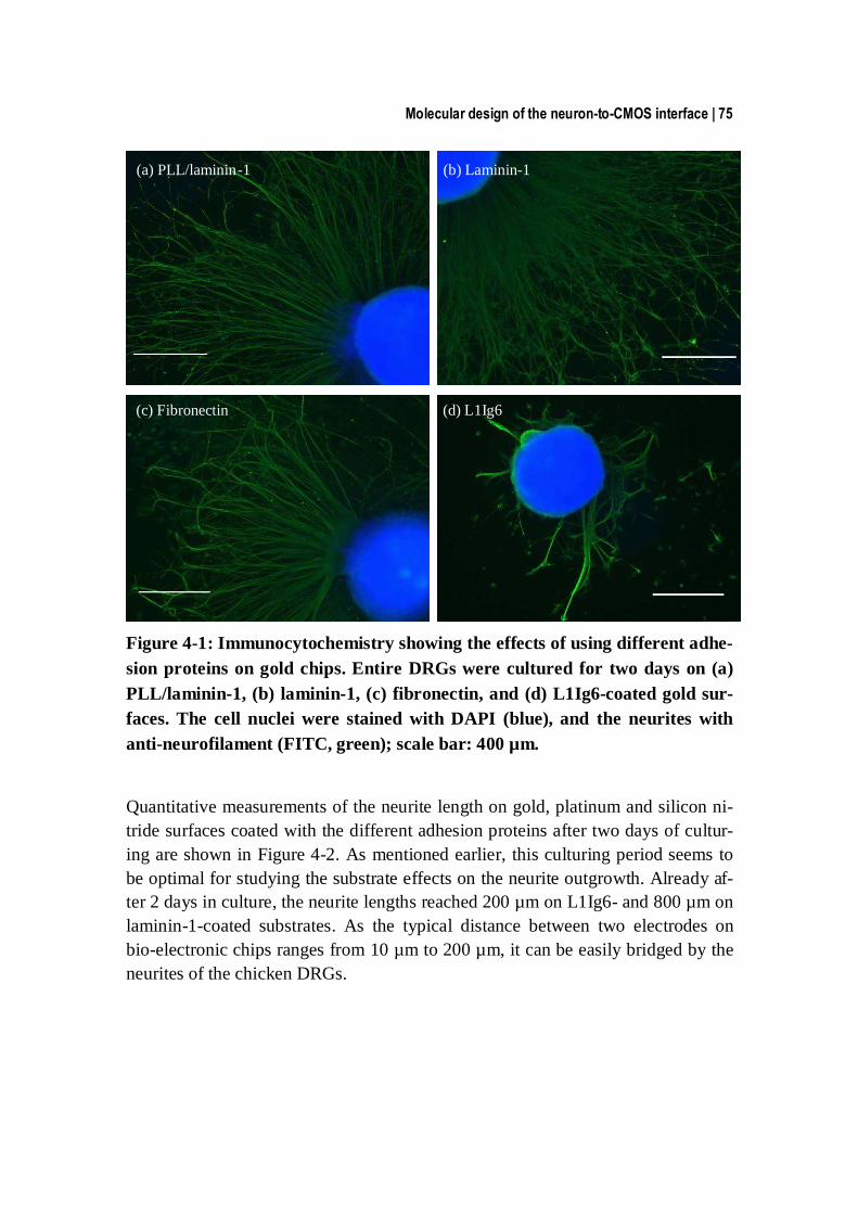
Molecular design of the neuron-to-CMOS interface | 75
Figure 4-1: Immunocytochemistry showing the effects of using different adhe-sion proteins on gold chips. Entire DRGs were cultured for two days on (a) PLL/laminin-1, (b) laminin-1, (c) fibronectin, and (d) L1Ig6-coated gold sur-faces. The cell nuclei were stained with DAPI (blue), and the neurites with anti-neurofilament (FITC, green); scale bar: 400 µm.
Quantitative measurements of the neurite length on gold, platinum and silicon ni-tride surfaces coated with the different adhesion proteins after two days of cultur-ing are shown in Figure 4-2. As mentioned earlier, this culturing period seems to be optimal for studying the substrate effects on the neurite outgrowth. Already af-ter 2 days in culture, the neurite lengths reached 200 µm on L1Ig6- and 800 µm on laminin-1-coated substrates. As the typical distance between two electrodes on bio-electronic chips ranges from 10 µm to 200 µm, it can be easily bridged by the neurites of the chicken DRGs.
(a) PLL/laminin -1 (b) Laminin-1
(c) Fibronectin (d) L1Ig6

76 | Chapter 4
Laminin-1 PLL & Laminin-1 Fibronectin L1Ig60
100
200
300
400
500
600
700
800
900
Neu
rite
leng
th [
m]
Gold Platinum Nitride
Figure 4-2: Entire DRGs cultured for 2 days on platinum, gold and silicon-nitride surfaces coated with different adhesion proteins (L1Ig6, laminin-1, PLL and laminin-1 and fibronectin).
It is noteworthy, that gold and platinum substrates showed a comparable neurite outgrowth. Both metals show similar protein adsorption characteristics and consti-tute suitable substrates that promote neurite extension. The neurite outgrowth on silicon-nitride surfaces coated with laminin-1, PLL/laminin-1, fibronectin and L1Ig6 seems to be very strong. However, we can-not exclude that this is due to experimental variations as these experiments were carried out at later date than the other experiments. This holds partially true since earlier experiments did not show such robust and long neurite outgrowth. Observa-tions on 1- and 4-day experiments showed that the outgrowth on nitride-coated substrates is generally comparable to that on platinum or gold. The results presented in Figure 4-1 and Figure 4-2 suggest that the protein layer determines the neurite number and the length of neurite extension and, hence, the network formation characteristics. The CMOS-surface materials do not seem to have a major influence on the cellular behavior.
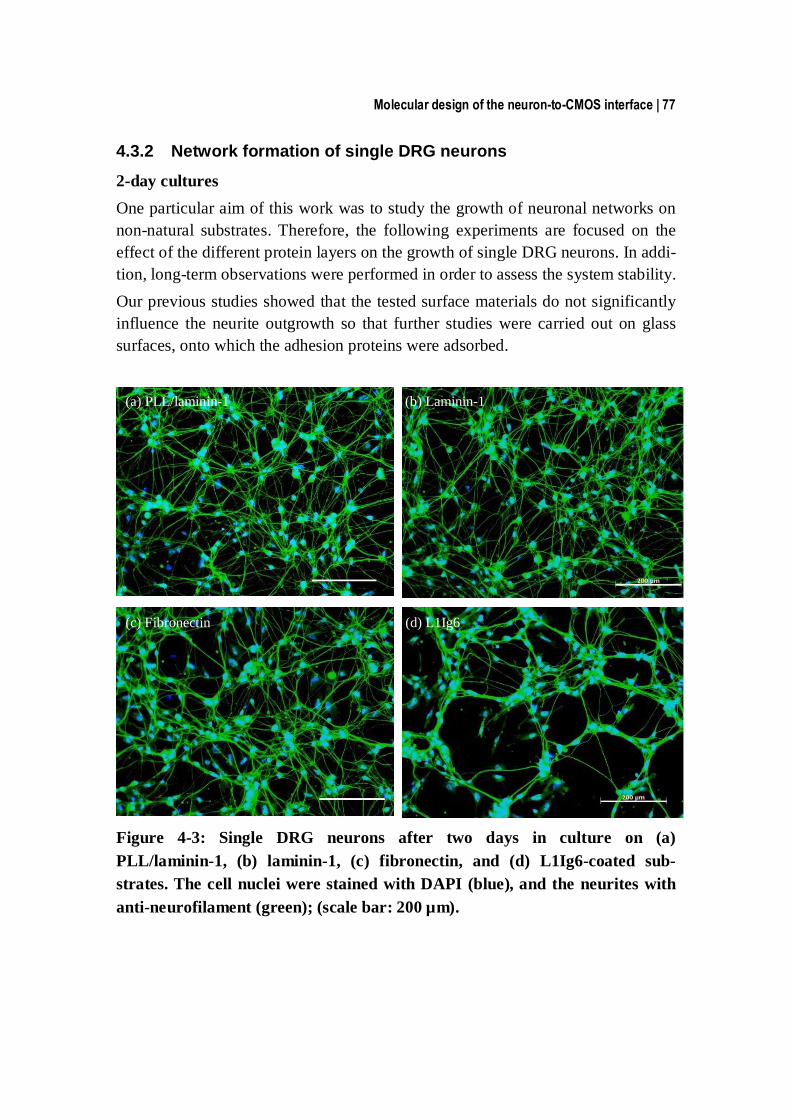
Molecular design of the neuron-to-CMOS interface | 77
4.3.2 Network formation of single DRG neurons
2-day cultures One particular aim of this work was to study the growth of neuronal networks on non-natural substrates. Therefore, the following experiments are focused on the effect of the different protein layers on the growth of single DRG neurons. In addi-tion, long-term observations were performed in order to assess the system stability. Our previous studies showed that the tested surface materials do not significantly influence the neurite outgrowth so that further studies were carried out on glass surfaces, onto which the adhesion proteins were adsorbed.
Figure 4-3: Single DRG neurons after two days in culture on (a) PLL/laminin-1, (b) laminin-1, (c) fibronectin, and (d) L1Ig6-coated sub-strates. The cell nuclei were stained with DAPI (blue), and the neurites with anti-neurofilament (green); (scale bar: 200 µm).
(a) PLL/laminin-1 (b) Laminin-1
(c) Fibronectin (d) L1Ig6

78 | Chapter 4
After two days in culture, dense neuronal networks on the different adhesive layers were formed, as shown in Figure 4-3. Note that cytosine ß-D-arabinofuranoside, (AraC) was supplemented to the culture medium to inhibit the proliferation of fi-broblasts. As expected from the experiments with entire DRGs, no differences in the network formation on PLL/laminin-1, laminin-1 and fibronectin could be ob-served. The neurons on the L1Ig6-coated substrates, though, showed again a different structure. Small cell clusters could be observed, which were connected by fascicu-lated neurites. These observations corresponded well to those of the entire DRGs as they also showed strong neurite fasciculation on L1Ig6-coated substrates. 8-day culture The characteristic of the networks was investigated after 8 days of cell culturing. A first visual impression revealed that the single DRG neurons formed functional and stable networks on laminin-1, fibronectin and L1Ig6 (Figure 4-4). However, a more detailed analysis showed differences between fibronectin- and laminin-1-coated substrates. The amount of non-neuronal cells on fibronectin was larger de-spite the fact that the same concentration of AraC was added to the culture me-dium. On laminin-1-coated substrates, considerably less fibroblasts were observed. These observations may be explained by the fact that laminin-1 is a good adhesive layer for neurons as it promotes the outgrowth of neurites (Beck, Hunter et al. 1990; Brandenberger and Chiquet 1995), whereas fibronectin preferably promotes the adhesion and proliferation of fibroblasts and Schwann cells. As it is intended to culture the cells for several weeks until the extracellular recordings can be per-formed, the proliferation of any non-neuronal cell should be avoided. After one week of culture, the cell bodies on L1Ig6-coated substrates formed even larger cell clusters than after 2 days. Although the initial plating density of the neurons was the same, the amount of non-fasciculated simple axons was much lower compared to laminin-1- and fibronectin-coated substrates. As the cells clus-tered together, the adhesion to the substrate was also weaker. In addition, the neu-ronal clusters tended to detach from the surface after a few days in culture.

Molecular design of the neuron-to-CMOS interface | 79
Figure 4-4 (a): Laminin-1-coated substrates. Sin-gle DRG neurons after one week in culture.
Figure 4-4 (b): Fi-bronectin-coated sub-strate. Note that the con-centration of non-neuronal cells is signifi-cantly higher than that on the laminin-1-coated substrate.
Figure 4-4 (c): L1Ig6-coated substrate. Fas-ciculation of the neurites is clearly visible.
(Scale bar: 200 µm)
Laminin-1
Fibronectin
L1Ig6

80 | Chapter 4
The issue of biocompatibility of the packaging materials is often underestimated. Thus, the last experiment in this section was targeted at analyzing the culturing of DRG neurons on poly(dimethylsiloxane) PDMS. Before the bio-electronic chips can be used for cell culturing, the bond wires, which connect the CMOS chip with e.g. a DIL (dual-inline) package, have to be sealed with a polymer for protection. The polymer is also used to form an incubation chamber for the cells. In most cases, the chosen packaging material is PDMS. To prove that PDMS is a biocom-patible material, PDMS was also coated with fibronectin, L1Ig6, laminin-1 and PLL/laminin-1. Entire DRG neurons were then cultured for one, two and four days. Figure 4-5 shows representative pictures after 2 days in culture. Cell adhe-sion and neurite outgrowth could be seen on all protein layers. Note that in this experiment, no Ara C was added to the medium. Therefore, the proliferation of the non-neuronal cells was not inhibited, which resulted in a ‘carpet-like’ formation of fibroblasts on the surface.
(a) Fibronectin (b) L1Ig6

Molecular design of the neuron-to-CMOS interface | 81
Figure 4-5: 2-day cultures showing neuronal outgrowth on protein-coated PDMS substrates. Entire DRGs were cultured on (a) fibronectin, (b) L1Ig6, (c) laminin-1, and (d) PLL/laminin-1-coated PDMS chips. Note that no Ara C was added to the culture medium (scale bar: 400 µm).
4.3.1 Visualization of the cell-to-electrode distance
The experiments shown above indicate that the adhesion protein determines the extent and the morphology of neurite outgrowth, the neurite fasciculation and the proliferation of non-neuronal cells. The next important consideration concerns the thickness of the protein layers, since the distance between cells and electrodes sig-nificantly influences the electrical coupling. The first set of images shows selected scanning electron microscope (SEM) im-ages of neurons cultured on the surface of a bio-electronic chip. In this case, the chip surface was coated with laminin-1 and the single DRG neurons were cultured for two days. The results are shown in Figure 4-6 (a)-(c). Figure 4-6 (a) gives an overview over cultured DRG neurons on the bio-electronic chip. The chip has sixteen 20×20 µm2 platinum electrodes, and a 500-nm silicon nitride layer serves as passivation layer. The proliferation of non-neuronal cells was inhibited by adding AraC to the culture. As expected, neurite outgrowth could already be observed after 2 days, and cell adhesion and neurite formation occurred as previously described. However, these images also illustrate that, although the neurons seem to contact the chip surface, a gap between the neurites and the sur-face of the chip is visible. Figure 4-6 (b) shows a higher magnification of two elec-trodes. The neurites seem not to touch the platinum surface but to adhere only to the edges of the electrode openings (highlighted by the white arrow). No explicit physical contact seems to exist between the neurites and the electrode. Figure 4-6
(c) Laminin-1 (d) PLL/laminin-1

82 | Chapter 4
(c) shows an adhering growth cone tightly attached to the surface. Although the surface topography of (b) and (c) is essentially the same, no visible gap between the growth cone-like structure and the laminin-1-coated surface could be detected. The growth cone adhered well to the surface of the platinum and the passivation layer despite the 500-nm step at the electrode opening. These SEM images suggest that the gap between the cell membrane and the elec-trode or chip surface shows rather strong width variations. In most cases, the neu-ronal cell bodies seem to indeed contact the chip surface, but this seems to hold only partially true for the neurites. This observation is interesting in the sense of functionality of such a network. Here, single chicken DRG neurons have been in-vestigated. These neurons never exist without their surrounding myelin sheath in vivo. These results might indicate that ‘naked’ neurites are not able to form close contacts to a substrate without a natural myelin sheath. This hypothesis has to be proven by further experiments. Moreover, one can conclude from these experi-ments that the chemistry of the adhesion-mediating layer determines the morphol-ogy and the adhesion of the neurons on a given surface. This might indicate that the electrical coupling is defined by the chemistry of the surface rather than the physical thickness of the layer. These aspects have to be investigated in more detail trying to exclude most of the possible experimental artifacts resulting from, e.g., the SEM sample preparation.

Molecular design of the neuron-to-CMOS interface | 83
Platinum electrodes
DRG neuron
(a)
(b)
10 µm
4 µm
Platinum electrodes
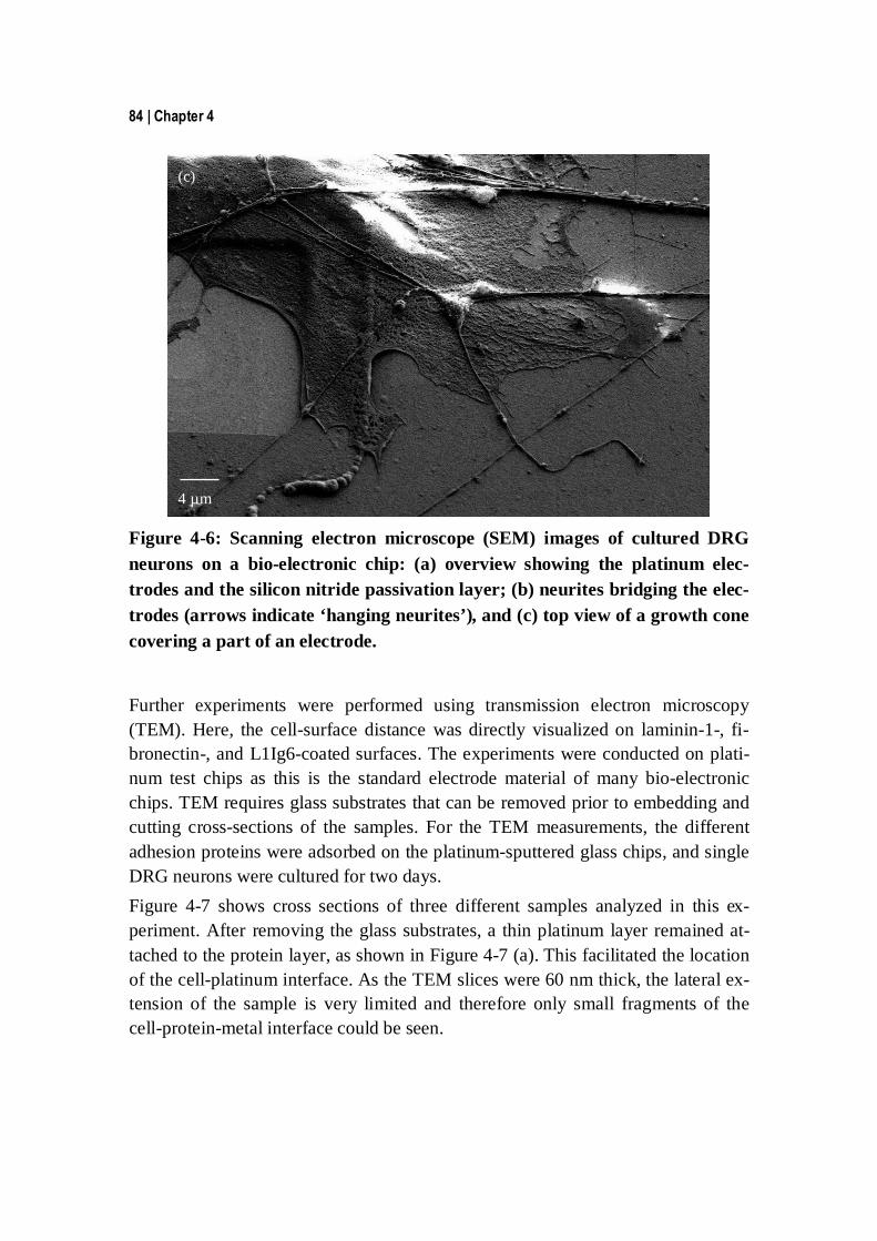
84 | Chapter 4
Figure 4-6: Scanning electron microscope (SEM) images of cultured DRG neurons on a bio-electronic chip: (a) overview showing the platinum elec-trodes and the silicon nitride passivation layer; (b) neurites bridging the elec-trodes (arrows indicate ‘hanging neurites’), and (c) top view of a growth cone covering a part of an electrode.
Further experiments were performed using transmission electron microscopy (TEM). Here, the cell-surface distance was directly visualized on laminin-1-, fi-bronectin-, and L1Ig6-coated surfaces. The experiments were conducted on plati-num test chips as this is the standard electrode material of many bio-electronic chips. TEM requires glass substrates that can be removed prior to embedding and cutting cross-sections of the samples. For the TEM measurements, the different adhesion proteins were adsorbed on the platinum-sputtered glass chips, and single DRG neurons were cultured for two days. Figure 4-7 shows cross sections of three different samples analyzed in this ex-periment. After removing the glass substrates, a thin platinum layer remained at-tached to the protein layer, as shown in Figure 4-7 (a). This facilitated the location of the cell-platinum interface. As the TEM slices were 60 nm thick, the lateral ex-tension of the sample is very limited and therefore only small fragments of the cell-protein-metal interface could be seen.
(c)
4 µm

Molecular design of the neuron-to-CMOS interface | 85
For all three proteins (laminin-1, fibronectin, and L1Ig6), a gap between the cells and the platinum layer could be observed. However, distinct characteristics can be observed for laminin-1-, fibronectin- and L1Ig6-coated surfaces. Laminin-1 for example, with a molecular weight between 700-800 kDa, forms a homogeneous and uniform layer and the cell-metal distance appears to be approximately 80 nm (Figure 4-7 (a)). Fibronectin in contrast, with a lower molecular weight of 440 kDa, leads to a smaller gap, and also shows characteristic adhesion sites (also known as focal contacts). At these focal contacts, the cellular structure is as close as approximately 40 nm to the metal surface. Apart from these contacts, the cells are at about 80 nm distance from the platinum (Figure 4-7 (b)). Although it was previously reported that DRG neurons are able to form focal contacts on fi-bronectin, but, not on laminin-1 (Gomez, Roche et al. 1996), it cannot be excluded that the image here shows a part of a fibroblast and not a neuron. In Figure 4-7 (c), DRG neurons cultured on L1Ig6, a protein with a small molecular weight of 8-10 kD, are shown. The cell membrane is separated from the metal by a very thin and rather uniform gap in the range of 20-50 nm. It has to be emphasized, that these data can only be used to determine cell-to-metal distances as the cell- and the protein layers might shrink during the TEM prepara-tion. Hints for a relative size can only be derived from the thickness of the plasma membrane, which is usually between 5-7 nm. The results presented give an indication of the minimum distance between cells and metal layers using different adhesive proteins. As the TEM images show only small fragments of the interface, one cannot reliably differentiate between the cell type (neuron, fibroblast or Schwann cell), or see whether it is a neurite, a growth cone or a cell body. Generally it was observed that the cell-to-chip distance on all three adhesive proteins strongly varies, since distances of up to 600 nm on all coat-ings could be observed, too. The results of the distance measurements are similar to the results obtained by the fluorescence-interferometry method published by Braun and Fromherz, which, however, was applied to living cells in a culture environment (Braun and From-herz 1998). These cell-to-surface distance measurements for laminin-1 and fi-bronectin yielded 100 nm and 60 nm, respectively.

86 | Chapter 4
(a) Laminin-1
(b) Fibronectin
Pt layer
Laminin layer
Cell layers
Focal contact
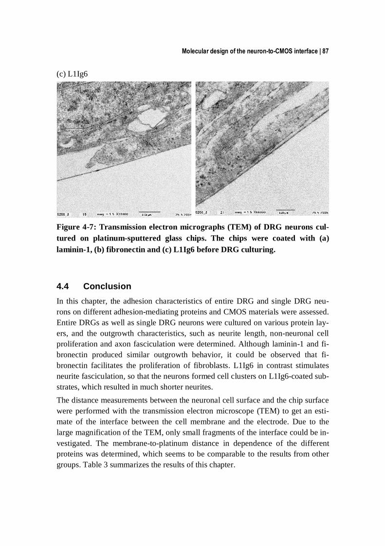
Molecular design of the neuron-to-CMOS interface | 87
(c) L1Ig6
Figure 4-7: Transmission electron micrographs (TEM) of DRG neurons cul-tured on platinum-sputtered glass chips. The chips were coated with (a) laminin-1, (b) fibronectin and (c) L1Ig6 before DRG culturing.
4.4 Conclusion In this chapter, the adhesion characteristics of entire DRG and single DRG neu-rons on different adhesion-mediating proteins and CMOS materials were assessed. Entire DRGs as well as single DRG neurons were cultured on various protein lay-ers, and the outgrowth characteristics, such as neurite length, non-neuronal cell proliferation and axon fasciculation were determined. Although laminin-1 and fi-bronectin produced similar outgrowth behavior, it could be observed that fi-bronectin facilitates the proliferation of fibroblasts. L1Ig6 in contrast stimulates neurite fasciculation, so that the neurons formed cell clusters on L1Ig6-coated sub-strates, which resulted in much shorter neurites. The distance measurements between the neuronal cell surface and the chip surface were performed with the transmission electron microscope (TEM) to get an esti-mate of the interface between the cell membrane and the electrode. Due to the large magnification of the TEM, only small fragments of the interface could be in-vestigated. The membrane-to-platinum distance in dependence of the different proteins was determined, which seems to be comparable to the results from other groups. Table 3 summarizes the results of this chapter.

88 | Chapter 4
Further investigations will include a combination of SEM images and focused-ion beam (FIB) to achieve both, a good overall representation of the neuronal network and high resolution-images of cross-section at a particular site to reveal more de-tailed characterization. Laminin-1 Fibronectin L1Ig6 PLL/laminin-1 Neurite extension
600-800 nm 600–650 nm approx. 200-400 nm (strong varia-tions)
approx. 600 nm
Shape robust out-growth
robust out-growth
axon fascicula-tion, compara-tively short neu-rite outgrowth
robust out-growth
Cell-to-chip dis-tance
80 nm 40-80 nm, forms focal contacts
20-50 nm not determined
AraC (0.4 µm)
inhibits prolif-eration of fi-broblasts
After 8-day culturing pe-riod, the fi-broblasts be-gin to over-grow the cul-ture
inhibits prolifera-tion of fibroblasts
not determined
Table 3: Summary of the DRG characteristics such neurite extension, shape of ganglia, cell-to-electrode distance and the inhibition of non-neuronal cell growth on laminin-1, fibronectin, L1Ig6 and the combination of PLL and laminin-1.

High-throughput cell-screening system | 89
5 Microchip High-Throughput Cell- Screening System with Integrated Dilution Stage
This chapter describes a fully integrated microchip device for performing a com-plete and automated drug-screening assay on living cells1. Cells were trapped and immobilized in a small 0.5-µl-volume incubation chamber by pneumatic anchor-ing on 1000 5-µm orifices and were then incubated for several days. Screening was performed with sample dilutions ranging over three orders of magnitude. A cascading, on-chip mixing structure considerably reduced the reagent consumption in comparison to conventional systems. The microsystem includes a perforated silicon chip embedded in a larger elastomer substrate, which features the microflu-idic network. This chapter describes the fabrication of the components and the assembly of the cell screening system, the validation of the drug diluter, cell-adhesion experiments over several days and a screening experiment with cultured normal human dermal fibroblasts (NHDFs), which were exposed to a fluorescent cell tracker.
5.1 Introduction Cell-based screening systems constitute a common method in pharmaceutical re-search to study drug-induced effects on cells. These screening systems are based on delivering drugs in a wide concentration range (3-6 orders of magnitude) to in-cubate cell populations. In standard systems, this process is performed in well plates (up to 1536 wells with effective volumes ranging from 1 to 100 µl), into which the cells and drugs are pipetted. The surface of these wells is usually pre-treated and can be coated with proteins such as poly-L-lysine, fibronectin or colla-
1 Livia Seemann is gratefully acknowledged for her excellent contribution in this project during her di-
ploma thesis.

90 | Chapter 5
gen to offer good adhesion conditions for the cells. The drugs are diluted off-line to their working concentration either manually or by automated robotic systems and are dispensed into the well plates, so that the cells and the respective drugs are separated from each other in different wells during incubation and screening. This technique is not only time and labor-intensive, it also requires large sample-compound quantities. To achieve low reagent consumption in a highly parallel drug-screening approach with integrated detecting or sensing step, a miniaturized equivalent of a microtiter plate and a dilution stage, both integrated in one system, are desired, so that several functions such as the immobilization and culturing of cells inside an incubation chamber, the drug dilution, and the drug-screening func-tions can be integrated. The immobilization of cells can be achieved using meth-ods such as physical retention chambers, where cells are trapped by an inserted cellulose-nitrate membrane (Tokuyama, Fujii et al. 2005), di-electrophoretic methods using an inhomogeneous electrical field (Manaresi, Romani et al. 2003; Gray, Tan et al. 2004), or the capturing of single cells either at the entrance of a silicon channel (Yun and Yoon 2005) or by pneumatic anchoring (Thielecke, Stieglitz et al. 1999; Greve, Lichtenberg et al. Manuscript in preparation). Also, multi-height ‘sandbag’-type structures were proposed for particle trapping (Li, Cheung et al. 2003). In addition to physical methods, surface-chemical strategies such as the use of adhesion proteins patterned by photolithography (Sorribas, Padeste et al. 2002), micro-contact printing (Whitesides, Ostuni et al. 2001) or the use of self-assembled monolayers, are promising approaches to facilitate the im-mobilization of cells on a chip surface (Lussi, Michel et al. 2004; Franks 2005). The mixing of a drug and a buffer solution to produce a wide concentration range is needed for drug-screening experiments. As manual dilution is hard to perform on low volumes, microfluidic diluters based on polymeric or inorganic materials were developed by several groups. Serial (Chang, Bang et al. 2003) and combined serial and parallel mixing (Jacobson, McKnight et al. 1999), combinatorial 3D mixing over several flow magnitudes (Neils, Tyree et al. 2004) and the use of dilu-tion gradients (Dertinger, Chiu et al. 2001) were proposed. As microfluidic mixers usually operate in the low-Renold’s-number regime, chaotic mixing was intro-duced to improve the mixing of the respective drug and buffer solutions (Stroock, Dertinger et al. 2002; Baier, Drese et al. 2005). Although a variety of miniaturized dilution stages were reported, the majority is limited to a dilution range of about two orders of magnitude. Here, a microchip-based system containing a miniaturized equivalent of a microtiter plate as well as a microfluidic dilution cascade is described. The device can be used for all essential

High-throughput cell-screening system | 91
steps of the screening process: (I) immobilization of a defined number of cells to yield a homogeneous array, (II) drug dilution, (III) incubation, and (IV) optical in-terrogation.
Chip
CellCell
PDMS
PDMS microfluidic system
Figure 5-1: System schematic: (i) silicon chip with perforated membrane em-bedded into PDMS; (ii) microfluidic system mounted on the chip after oxy-gen-plasma activation.
5.2 Device description and modeling A schematic of the device is shown in Figure 5-1. The microsystem consists of three distinct components: (a) a 75-mm2 silicon chip with an array of 1000 ori-fices for cell trapping, (b) 22-cm2 elastomeric substrate, into which the chip is embedded, to enlarge the real estate of the device, and (c) a microfluidic cover with the integrated diluter cascade, made of poly(dimethylsiloxane) (PDMS) (Figure 5-2). After assembly, the diluter, a 0.5-µl incubation chamber and the cell-loading ports constitute a single unit. A cell screening with this device is per-formed as follows: first, a cell suspension is pumped through the incubation cham-ber, and the cells are trapped on the orifices. This assures a homogeneous cell dis-tribution inside the chamber. Then, the excess cells are washed away by a laminar buffer stream to leave the chamber with a defined number of cells in a homogene-ous arrangement. Cells are only immobilized during loading and can afterwards proliferate freely during the incubation step. The cells are typically incubated for

92 | Chapter 5
several days before the actual screening process is performed. For screening, only a minute amount of the drug is pumped into one inlet of the dilution cascade, where it is mixed with a buffer solution from the other inlet to yield the relative final concentrations of 100%, 10%, 1%, 0.1%, 0% of the drug. The five diluter outputs provide laminar streams over the respective areas of the immobilized cells, so that each stream only perfuses a defined part of the overall cell area. Simultane-ously or sequentially, the cellular response can be optically assessed by e.g. adding specific fluorescent tags to the buffer stream.
5.2.1 Silicon orifice chip
The cells are immobilized on the silicon chip by individual trapping on an array of 5×200 orifices due to a slight pressure difference between the inside and the out-side of the incubation chamber. Typically, a single cell is immobilized on one ori-fice during this process. This technique, denoted as ‘pneumatic anchoring’, has been previously described by (Thielecke, Stieglitz et al. 1999) and by our group (Greve, Lichtenberg et al. Manuscript in preparation) for bio-electronic CMOS chips. Cell immobilization is used here for mainly two reasons. First, the technique allows for loading the chamber with an exactly defined number of cells for each experiment. Consequently, the resulting fluorescence intensity measurements lead to reproducible and statistically relevant data for the different drug concentrations. Second, a homogeneous cell carpet is obtained due to the equal spacing between the orifices; without immobilization features, the cell loading would lead to irre-producible and spatially imbalanced cell populations that are not suitable for screening experiments. After the loading step has been completed, the immobiliza-tion force has been found not to disturb the cell proliferation. Although cells might migrate during the incubation, the homogeneous nature of the cell carpet is pre-served. As the diameter of the cells used in this project, normal human dermal fibroblasts (NHDFs), is approximately 20 µm, orifices in the range of 5 µm need to be fabri-cated to prevent any suction of the cells through the orifices. Silicon was used as the chip material, because of the available precision etching techniques. Orifices were etched from the frontside by reactive-ion etching, while the chip back-side was thinned by anisotropic wet etching to a 5-µm membrane to reduce the lateral widening of the orifices during fabrication. As silicon technology is comparably expensive, the chip size is limited to the absolute necessary area (7×5 mm2). To have enough space around this chip for the integration of the microfluidics, the chip was seamlessly embedded into a larger, 2×2-cm2 PDMS substrate before the

High-throughput cell-screening system | 93
microfluidic cover was bonded onto the chip. No leakage of drugs into the cleft between the chip and the microfluidic system was observed.
5.2.2 Microfluidic system
All the necessary parts for the drug handling were integrated into the microfluidic cover (Figure 5-2). The orifice array is covered by a 0.5-µl incubation chamber (3.5 mm wide, 1.4 mm long, and 100 µm high). Two loading ports (5 mm long) are provided to inject the cell suspension into the incubation chamber. The cell loading stream is perpendicular to the main buffer stream. Two inlets are provided for the buffer solution and the drug stock, which are mixed in the cascading dilu-tion stage to produce the desired concentrations. Five outlets (100 µm wide, 700 µm spacing) provide the drug dilution to five cell arrays. On the opposite side of the chamber, a symmetrical shape port leads to the waste reservoir.
Figure 5-2: Micrograph of the cell-screening system with the online diluter, the 0.5-µl incubation chamber and the cell-loading ports (channel contrast emphasized).
As microfluidic devices generally operate in the laminar-flow regime, mixing in the dilution stage is only achieved by diffusion. For the structure presented here this also holds true as the Reynold’s number is between 0.1 and 2, which is far be-low the threshold for turbulent flow. To ensure complete mixing, the channel ge-
Inlets for drug and buffer
Cell loading ports
Incubation chamber
Waste outlet 1 cm

94 | Chapter 5
ometries have to be adapted in terms of width and length, and the corresponding flow rates have to be chosen accordingly. The mixing ratios are defined by the flow rates of the drug and the buffer solution at the branches of the diluter stage. At each interception point, the flow rate of the incoming drug (or output of the previous dilution stage) is 9 times smaller than the flow rate of the buffer to obtain the desired dilution of 1: 9. Thus, using three cascading levels with three intercep-tion points, dilutions of 10%, 1%, 0.1% can be achieved. This modular design can be extended to more dilution levels and can be adapted to different dilution ratios. Concentration errors in each stage propagate to the next level so that a careful de-sign and fabrication of this structure are essential. While the residence time of drug molecules in the diluter branches must be long enough to assure complete mixing, the residence time in the incubation chamber must be as short as possible to avoid unwanted interference between neighboring drug streams. The design re-quirements for the diluter and the incubation chamber are therefore strongly inter-related, and an optimization is necessary.

High-throughput cell-screening system | 95
l
a
LDiffmax
Orifices/Cells
Figure 5-3: Design considerations of the microfluidic incubation chamber with a denoting the distance between two incoming laminar streams, l the chamber length and LDiffmax the maximally allowed diffusion to avoid interfer-ence between neighboring streams, i.e. concentration gradients within one cell bed. (a = 200 µm, l = 1400 µm; LDiffmax = 100 µm)
5.2.3 Design and modeling approach
Figure 5-4 shows a schematic of the incubation chamber. The five individual streams are flowing from the dilution stage into the chamber, where the cells are immobilized and brought into contact with the drugs. The boundary conditions for the chamber design are as follows:
1. Mixing of the adjacent streams within the incubation chamber should not cause interference between two neighboring cell beds.
2. The flow rates Q1 to Q5 within the incubation chamber must be the same to provide an equal width of the drug streams in the incubation chamber.

96 | Chapter 5
Diffusion in the chamber causes a widening of the concentration profiles inside the incubation chamber. The maximal diffusion length, which is still acceptable, is given by
(1) 2maxaLDiff with a denoting the spacing between
two orifice beds. The maximum residence time in the chamber that is allowed without mixing to oc-cur is given by
(2) 22
max
82 Da
DL
t Diff with D as the diffusion constant.
Consequently, the minimum required flow rate can be calculated by:
(3) t
lAQ min with A as the chamber cross-section
l as the chamber length. For the device described in this chapter, the minimum flow rate inside the incuba-tion chamber should be at least 5.88 µL min-1 taken all design parameters into ac-count (a = 200 µm; D = 10-9 m2s-1 for a typical biomolecule; A = 0.35 mm2; l = 1.4 mm).

High-throughput cell-screening system | 97
9:1
9:1
0% 0.1% 1% 10% 100%Q1 Q2 Q3 Q4 Q5
Qbuffer QDrug
9:1
(a)
Q1 Q2 Q3 Q4 Q5
Qbuffer QDrug
1 1 1 1 1
1.9
2.89
3.889
1.1
1.110.99 0.11
0.999 0.1111.111
0.10.9
(b)
Figure 5-4: Schematic of (a) the whole microfluidic design and (b) the dilution stage with the different flow rates in each branch.
Figure 5-4 (a) shows a schematic of the diluter: For both inputs, the buffer solution and the drug stock solution are directly connected to the ports 1 and 5 thus provid-ing 0% and 100% streams. The diluter is realized as a cascading structure with three stages that mix the two solutions to the desired concentrations and connect these to the ports 2 to 4. The requirements for the dilution stage are: 1. Mixing ratios are based on the different flow rates. 2. The output flow rates of the dilution stage Q1 to Q5 are equal (normalized to 1
in this discussion). 3. The drug concentrations of Q1 to Q5 should be C5 = 10·C4 = 100·C3 =
1000·C2 and C1 = 0 leading to relative concentrations of 100%, 10%, 1%, 0.1%, and 0% of the drug stock solution.
The mixer structure has been designed using a lumped-element, equivalent-circuit model, in which each channel segment is represented by an electrical resistor. The individual flow rates and the resulting resistances of each branch can be deter-mined by solving the linear system of equations derived from the equivalent cir-

98 | Chapter 5
cuit using Kirchhoff’s theory. The flow rate corresponds to an electrical current and the flow resistance to an electrical resistance. The individual flow rates can be calculated using Kirchhoff’s nodal rule as shown in Figure 5-4 (b). For the diluter output stream Q2 with a normalized flow rate of 1, the ratio of the both incoming streams is 9:1 leading to a flow rate in the branches of 0.9 and 0.1, respectively (at each node the sum of the incoming currents equals the outcoming current). The flow rates in the other branches can now be calculated bottom-up. The results are shown in Figure 5-4 (b). To achieve complete mixing in each branch of the diluter, a minimum residence time has to be assured. This condition is met for the overall system, if it is fulfilled for the mixing branch with the highest flow rate and the shortest channel length (marked with the grey box in Figure 5-4 (b)). If mixing can be guaranteed in this branch, the liquids in all other channels will be completely mixed as well. The flow rate of the mixing channel can be calculated by first determining the flow rates in the diluter output streams Q1 to Q5. As all five branches of the diluter have the same flow rate and all drug streams are directed into the incubation chamber, the outlet flow rates Q1 to Q5 can be determined by
(4) 551
chamberQQ with Qchamber as the minimum flow rate in the chamber.
The flow rate and the time required for a complete mixing can then be calculated by (5) 5111.1 QQchannel with Qchannel as the flow rate of the
shortest channel and
(6) D
Lt channelchannel 2
2
with Lchannel as half width of the mix-ing channel
leading to a minimum channel length of
(7) A
tQl channelchannelchannel
and a minimal channel-to-chamber-length ratio of
(8) 11.11))((
51 2
maxDiff
channel
channel
chamber
chamber
channel
LL
AA
ll
The minimum required length of the channel to ensure complete mixing is then 2.7 mm for the given parameters (Achannel = 0.01 mm2; Q1-5 = 1.176 µL min-1;
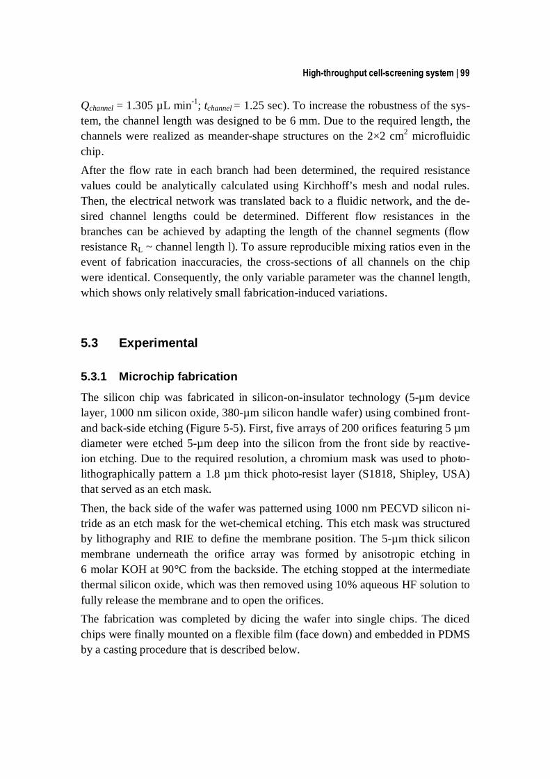
High-throughput cell-screening system | 99
Qchannel = 1.305 µL min-1; tchannel = 1.25 sec). To increase the robustness of the sys-tem, the channel length was designed to be 6 mm. Due to the required length, the channels were realized as meander-shape structures on the 2×2 cm2 microfluidic chip. After the flow rate in each branch had been determined, the required resistance values could be analytically calculated using Kirchhoff’s mesh and nodal rules. Then, the electrical network was translated back to a fluidic network, and the de-sired channel lengths could be determined. Different flow resistances in the branches can be achieved by adapting the length of the channel segments (flow resistance RL ~ channel length l). To assure reproducible mixing ratios even in the event of fabrication inaccuracies, the cross-sections of all channels on the chip were identical. Consequently, the only variable parameter was the channel length, which shows only relatively small fabrication-induced variations.
5.3 Experimental
5.3.1 Microchip fabrication
The silicon chip was fabricated in silicon-on-insulator technology (5-µm device layer, 1000 nm silicon oxide, 380-µm silicon handle wafer) using combined front- and back-side etching (Figure 5-5). First, five arrays of 200 orifices featuring 5 µm diameter were etched 5-µm deep into the silicon from the front side by reactive-ion etching. Due to the required resolution, a chromium mask was used to photo-lithographically pattern a 1.8 µm thick photo-resist layer (S1818, Shipley, USA) that served as an etch mask. Then, the back side of the wafer was patterned using 1000 nm PECVD silicon ni-tride as an etch mask for the wet-chemical etching. This etch mask was structured by lithography and RIE to define the membrane position. The 5-µm thick silicon membrane underneath the orifice array was formed by anisotropic etching in 6 molar KOH at 90°C from the backside. The etching stopped at the intermediate thermal silicon oxide, which was then removed using 10% aqueous HF solution to fully release the membrane and to open the orifices. The fabrication was completed by dicing the wafer into single chips. The diced chips were finally mounted on a flexible film (face down) and embedded in PDMS by a casting procedure that is described below.

100 | Chapter 5
Silicon
Silicon
Silicon dioxide
Silicon nitridepassivation
KOH etching
HF etching
(0.1 µm)
5 µm
380 µm
Figure 5-5: Silicon microchip fabrication: the silicon wafer was photolitho-graphically patterned, and the orifices were etched from the front side using RIE. Then, the back side was patterned using 1000 nm silicon nitride before anisotropic KOH etching of the silicon. Finally, the membrane was fully re-leased by isotropic etching of the intermediate silicon-oxide layer with HF.
5.3.2 Fabrication of the microfluidic device
The microfluidic network was formed in a second chip which was fabricated in PDMS by casting from a silicon mold featuring 100-µm-high SU-8 structures. The fabrication process was as follows: After dehydration of the silicon wafer, the SU-8 (SU-8 50, Microchem, USA) was spun onto the wafer (1250 rpm) and a two-level soft-bake (60°C for 1 min, 95°C for 75 min) was performed on a hotplate to evaporate the solvents and to harden the photo resist. The hotplate was switched off after the bake to let the wafer cool down slowly. Then, the UV-exposure in the

High-throughput cell-screening system | 101
mask aligner (energy dose 600 mJ/cm2) was done to transfer the desired fluidic pattern from a typesetting film mask (8 µm resolution) onto the wafer. The post-exposure bake was carried out at 65°C (1 min) followed by 95°C (45 min), before the wafer was developed in Microchem’s SU-8 developer for 10 min and washed with isopropanol. The fabrication was completed with the hard bake at 150°C to achieve a better mechanical stability. The PDMS replica mold was first pre-treated with the surfactant Triton-X 100 (0.05% in water), which was applied by spin coating at 1000 rpm and then dried at ambient temperature. The surfactant was needed to facilitate the mold release of the PDMS. Then, the PDMS (Sylgard 184, Dow Corning, USA) was prepared with a weight ratio of 10:1 for component A and B followed by degassing in a vacuum chamber for 30 min. The PDMS was finally poured onto the wafer and cured at 60°C for 4 hours. After removing the PDMS layer from the master, the cast was rinsed thoroughly in warm water to remove Triton-X residues that might prevent bonding, and was cut into single chips.
5.3.3 Embedding of the silicon chip
The silicon chip and the microfluidic PDMS chip have dimensions of 7×5 mm2 and 20×20 mm2, respectively. To prevent leaking of drugs through a cleft between these two devices, a tight seal between the silicon chip and the microfluidic cover was necessary. For that reason, the silicon chip was embedded into a PDMS sup-port to form a flat surface. The chip was first placed upside-down on a flexible polypropylene film, then, the cavity underneath the membrane was sealed by a 3×3 mm2 teflon bolt, which was pressed against the chip. The PDMS was poured around the chip and cured for 4 hours on a hotplate at 60°C. Finally, the bolt was released and the plastic film was removed from the front side leaving the silicon chip seamlessly embedded in the PDMS. To assemble the complete device, the PDMS microfluidic unit was irreversibly bonded onto the embedded silicon chip after oxygen-plasma activation for 30 sec, 100 W.
5.3.4 External setup
Pipette tips (1 ml, Roth AG, Germany) were used to fill the incubation chamber with the cell suspension. For the drug-screening experiments, a stepper-motor-driven syringe pump (PicoPlus, Harvard Apparatus, USA) was used to provide the required flow rates. Two glass syringes (ILS GmbH, Germany) with volumes of 250 µl and 1000 µl to provided a flow-rate ratio of 1:4 of the drug stock and buffer

102 | Chapter 5
solution were connected via dispensing needles (1 mm diameter, Panacol, Ger-many) to the microfluidic device.
5.3.5 Chamber pretreatment
Before the cells could be loaded, the assembled overall device was cleaned with ethanol and exposed to an oxygen plasma at 80 W for 30 min to render the surface of the PDMS less hydrophobic. Directly after removing the device from the plasma furnace, the incubation chamber was coated with the adhesion-mediating protein laminin-1 (20 µg/ml in TBS, Sigma Aldrich) for improved cell adhesion. The chip was then incubated for 30 min, 37°C, 5% CO2 before washing with TBS.
5.3.6 Cell preparation
During the course of the experiments, a normal human dermal fibroblasts (NHDF) stock was cultured (Promocell, Germany, C-12300). Before each cell loading, the medium was removed from the fibroblasts and the cells were washed with TBS. Then, 0.25% trypsin (Invitrogen Switzerland, 06354) in DMEM (Invitrogen, 21885-025) was added (3 min, 37°C) to detach the cells from the surface of the Petri dish. The trypsin reaction was stopped with DMEM containing 10% FBS (Fetal Bovine Serum, Sigma, F1051) (at least 3 times the amount of trypsin) and was then centrifuged at 1500 rpm before the supernatant was removed from the cells, and fresh medium was added. The cell clusters were then detached from each other by gently pipetting the cell suspension back and forth.
5.3.7 Cell loading
The cell suspension was filled into a pipette tip, which was connected to one of the inlets of the cell loading ports. As the liquid level in this loading port was higher than in the other empty one, a hydrostatic flow of cells into the incubation cham-ber was generated. The hydrostatic pressure difference between the inside and the outside of the incubation chamber also induced a minute flow through the orifices, so that single cells were trapped and were immobilized on the orifices. The cells were immobilized in five separate colonies of 200 cells each, so that the system provided a defined number of cells and a homogeneous cell density (Figure 5-6). Due to the larger specific density of the fibroblasts, the cells tend to sediment in the loading pipette. As a result, the cell concentration decreased permanently dur-ing the loading process until finally clear medium flowed through the chamber. As soon as all the orifices were occupied by cells, the remaining excess cells were,

High-throughput cell-screening system | 103
therefore, washed away. In fact, the cells were only retained in the chamber due to the pneumatic anchoring through the orifices. A control experiment using a cham-ber without orifices yielded the result that no cells remained in the chamber. During cultivation, the loaded device was placed in a Petri dish, which was filled with 2 ml of medium to prevent the drying out of the cells in the incubation cham-ber. The medium was exchanged once a day by hydrostatic flow using a medium-filled pipette tip connected to one of the cell loading ports.
Figure 5-6: Cell immobilization: Micrograph of fibroblasts (20 µm diameter) immobilized on the orifices of the silicon chip so that a homogenous cell den-sity was achieved.
5.4 Results & Discussion
5.4.1 Validation of the drug diluter architecture
The performance of the drug diluter was first validated qualitatively using blue food color. For this experiment, the microfluidic device was bonded onto a glass microscope slide to be able to monitor the different color intensities under an in-verted microscope.
100 µm

104 | Chapter 5
As calculated by our model, the flow rates were set to a ratio of 1:4 for the drug inlet and the buffer inlet at a total flow rate of 1.875 µl/min. Figure 5-7 shows a micrograph of the diluter with the three mixing stages. The mixing of the color and the buffer solution with a dilution ratio of 9:1 at each node could be qualitatively observed. After mixing, the drug and the buffer flowed through the long meander-shape channels, which facilitated complete interdiffu-sion. When entering the incubation chamber, all drug streams were fully mixed, and five laminar streams of equal width through the chamber could be observed. At the entrance of the chamber, the streams were completely separated from each other; further down a small degree of diffusion between the streams in the chamber could be ob-served, as expected. However, the streams remained clearly separated and no major interdiffusion between the neighboring zones could be observed. Moreover, the cell beds were spaced at a large enough distance and there was no concentration gradient over one of the cell beds.
Figure 5-7: Micrograph of the microfluidic diluter which was qualitatively verified with DI water and blue food color as drug replacement. The black boxes showed the first, second and third dilution stage to produce relative concentrations of 10%, 1% and 0.1%. The picture was assembled from sev-eral micrographs taken during a single experiment. Dotted lines indicate channel outside the viewable area.

High-throughput cell-screening system | 105
For a quantitative evaluation, an aqueous 100-µM fluorescein solution (di-sodium fluorescein, Sigma Aldrich) was filled into the drug inlet, and distilled water was filled into the buffer inlet. The fluorescence intensity was measured using a modi-fied inverted epi-fluorescence microscope with a photomultiplier module (PMT H5784, Hamamatsu Photonics, Japan) attached to the camera port. The light emis-sion from the chip was first spatially discriminated using a 1-mm pinhole and fil-tered using a 525-nm metallic interference filter (Edmund Optics, USA). Figure 5-8 shows a plot of the calculated and the experimentally determined relative fluorophore concentrations. The graph shows that the fluorescence intensities pro-duced at the outputs of the dilution cascade corresponded very well to the desired concentrations. As the dilution of the different concentrations was achieved by a cascading structure, the deviation between the desired and achieved concentrations became larger from stage to stage yielding a maximum relative mismatch of 30% for the 0.1% dilution stage. However, this variation can be attributed to geometri-cal imprecisions in the microfluidic network as a consequence of the low resolu-tion of the photolithographic mask. With a standard chromium mask, a signifi-cantly better result is expected.
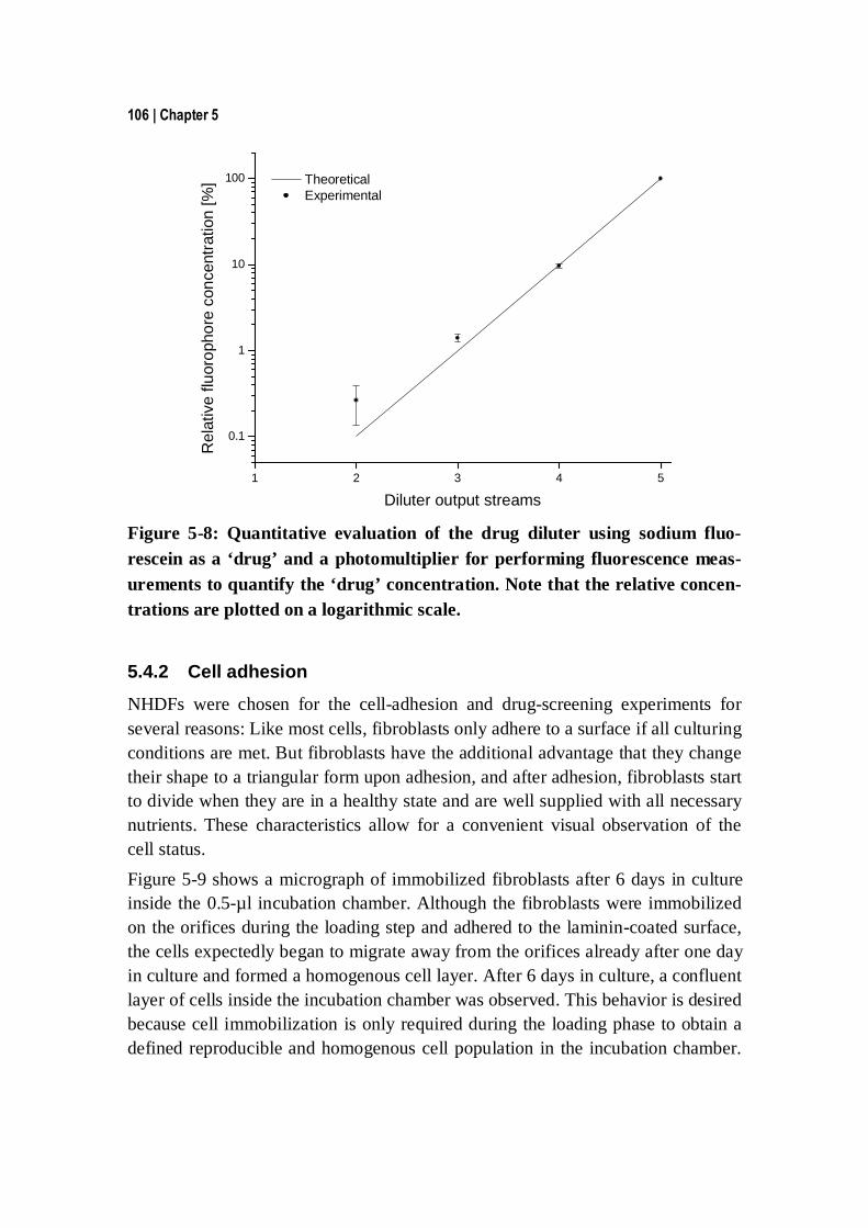
106 | Chapter 5
1 2 3 4 5
0.1
1
10
100
Rel
ativ
e flu
orop
hore
con
cent
ratio
n [%
]
Diluter output streams
Theoretical Experimental
Figure 5-8: Quantitative evaluation of the drug diluter using sodium fluo-rescein as a ‘drug’ and a photomultiplier for performing fluorescence meas-urements to quantify the ‘drug’ concentration. Note that the relative concen-trations are plotted on a logarithmic scale.
5.4.2 Cell adhesion
NHDFs were chosen for the cell-adhesion and drug-screening experiments for several reasons: Like most cells, fibroblasts only adhere to a surface if all culturing conditions are met. But fibroblasts have the additional advantage that they change their shape to a triangular form upon adhesion, and after adhesion, fibroblasts start to divide when they are in a healthy state and are well supplied with all necessary nutrients. These characteristics allow for a convenient visual observation of the cell status. Figure 5-9 shows a micrograph of immobilized fibroblasts after 6 days in culture inside the 0.5-µl incubation chamber. Although the fibroblasts were immobilized on the orifices during the loading step and adhered to the laminin-coated surface, the cells expectedly began to migrate away from the orifices already after one day in culture and formed a homogenous cell layer. After 6 days in culture, a confluent layer of cells inside the incubation chamber was observed. This behavior is desired because cell immobilization is only required during the loading phase to obtain a defined reproducible and homogenous cell population in the incubation chamber.

High-throughput cell-screening system | 107
Once the initial population is successfully established the cells should freely pro-liferate to form a confluent layer.
Figure 5-9: Micrographs of incubated normal human dermal fibroblasts (NHDFs) after 6 days in culture.
5.4.3 Drug screening experiments with cell trackers
To mimic a typical drug-screening procedure, the absorption of a fluorescent cell tracker by immobilized NHDFs from differently diluted streams of the fluorophore was studied. Before incubation, the chamber was coated with laminin-1 (20 µg/ml in TBS) for 30 min before cell loading. Cell preparation and loading was per-formed as described in the experimental section. In this experiment, the dilution and cell-exposure process was started already 30 min after immobilization. Green cell tracker (CellTracker Green CMDA C2925, Molecular Probes) with a stock concentration of 100 µM was diluted to 10 µM, 1 µM, 0.1 µM and 0 µM with me-dium in the diluter stage. The cells were exposed to the five laminar streams of different concentrations at a total flow rate of 1.25 µl/min for 20 min. Then, the syringe pump filled with the cell tracker solution was stopped, while the second pump with the medium continued operation to flush the chamber. The presence of the cell tracker was optically monitored as shown in the fluorescence image in Figure 5-10. The concentrations increased from the left to the right. A correlation between the cell tracker concentration and the fluorescence intensity in the cell beds was observed.
50 µm
150 µm

108 | Chapter 5
Figure 5-10: Fluorescence image of cells stained by a cell tracker in the incu-bation chamber; right: highest cell tracker concentration; left: lowest cell tracker concentration. The total cell tracker flow rate was 1.25 µl/min for 20 min.
A more quantitative analysis is shown in Figure 5-11 and was performed by image analysis of the acquired digital fluorescence images using the Lspix-5.1 (National Instruments of Standards, USA) software package. The average brightness of a rectangular area over each of the five cell beds comprising 64000 pixels was de-termined and plotted for each drug stream. While the higher-concentration streams produced significantly different fluorescence intensity in the cell beds, the 0-µM and 0.1-µM streams produced more fluorescence than expected. We attribute this to accidental contamination of the low-concentration streams with the cell tracker during starting the drug pump, which might have led lead to an intermittently in-creased drug concentration in streams 1 and 2 before a steady state was estab-lished. Figure 5-11 also illustrates that the absorption of the dye in the cell caused a non-linear relationship between the cell tracker concentration in the stream and the corresponding cell fluorescence intensity (note that the drug concentrations are logarithmic). No major cross contamination between the neighboring streams and cell beds was observable, so that the system met all requirements for the integrated cell-screening system.
500 µm
0% 0.1% 1% 10% 100%
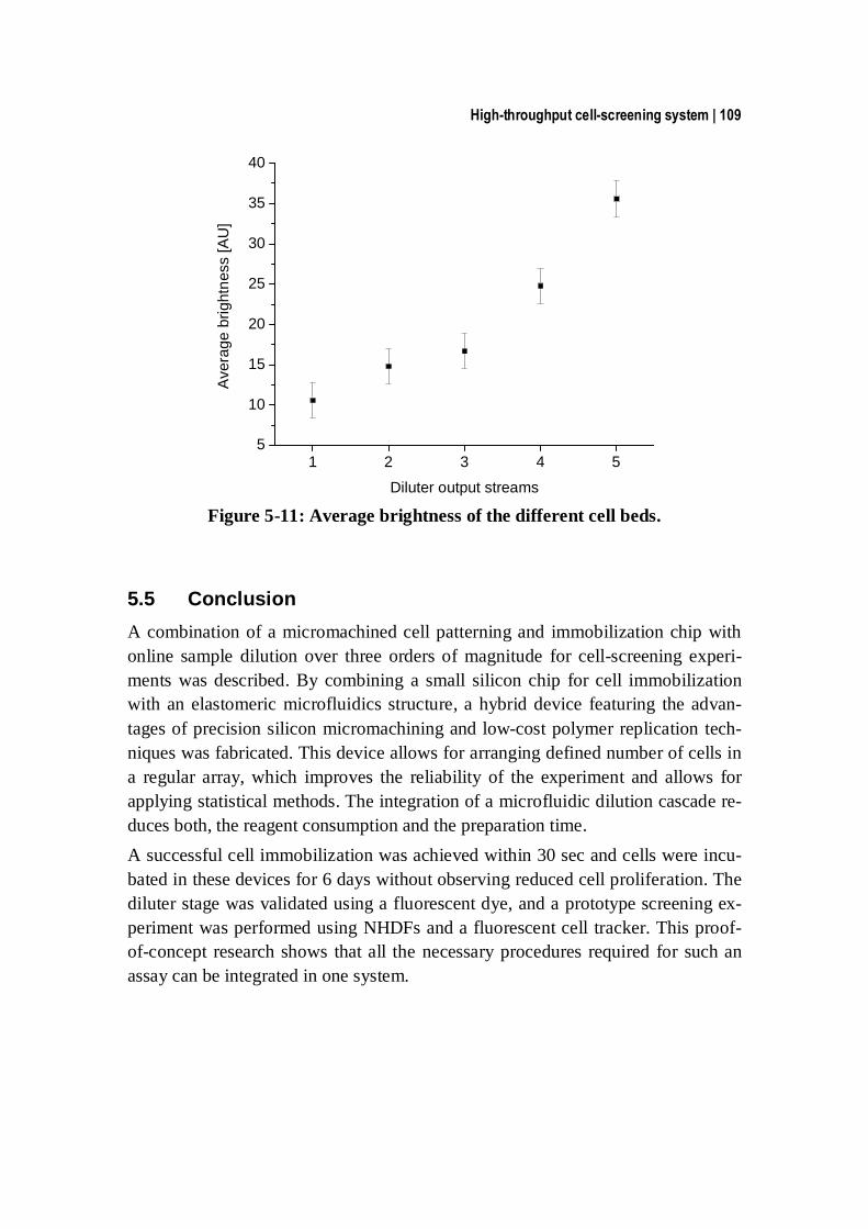
High-throughput cell-screening system | 109
1 2 3 4 55
10
15
20
25
30
35
40
Ave
rage
brig
htne
ss [A
U]
Diluter output streams Figure 5-11: Average brightness of the different cell beds.
5.5 Conclusion A combination of a micromachined cell patterning and immobilization chip with online sample dilution over three orders of magnitude for cell-screening experi-ments was described. By combining a small silicon chip for cell immobilization with an elastomeric microfluidics structure, a hybrid device featuring the advan-tages of precision silicon micromachining and low-cost polymer replication tech-niques was fabricated. This device allows for arranging defined number of cells in a regular array, which improves the reliability of the experiment and allows for applying statistical methods. The integration of a microfluidic dilution cascade re-duces both, the reagent consumption and the preparation time. A successful cell immobilization was achieved within 30 sec and cells were incu-bated in these devices for 6 days without observing reduced cell proliferation. The diluter stage was validated using a fluorescent dye, and a prototype screening ex-periment was performed using NHDFs and a fluorescent cell tracker. This proof-of-concept research shows that all the necessary procedures required for such an assay can be integrated in one system.


Conclusion and Outlook | 111
6 Conclusion and Outlook 6.1 Conclusion The work of this thesis was aimed at improving techniques for microchip-based cell-monitoring systems. This goal has been pursued in three different but related projects: (1) The investigation of biocompatible substrates for stable neuronal networks on microelectrode-arrays (MEAs), (2) the development of a CMOS mi-croelectronic chip with integrated cell-immobilization features, and (3) the appli-cation of this cell-placement technique within a fully integrated drug-screening system. First, a detailed biocompatibility study with over 300 samples was performed for a systematic investigation of cell adhesion and differentiation on different adhe-sion-promoting protein layers adsorbed onto CMOS surfaces. The characteristic outgrowth of embryonic chicken neurons from dorsal root ganglia (DRGs) was analyzed during a time span between two and eight days in culture. It was found that the DRG neurons adhere and differentiate best on laminin-1-coated substrates. This protein elicits the outgrowth of neurites, while it does not facilitate the prolif-eration of fibroblasts. A laminin-1 concentration of 10 µg/ml in TBS seems to be optimal for the formation of the adhesion layer on all substrates tested in this work, i.e., platinum, silicon nitride and gold. Second, a reliable cell-placement technique, physical immobilization by means of pneumatic anchoring was developed with the aim to automatically and precisely place cells on the chip surface. As a proof of concept, a CMOS-based, bio-electronic chip with perforated electrodes was developed and characterized. Pneumatic anchoring allowed to precisely place multiple single cells in the center of the respective electrodes in a parallel fashion. The electrical activity of, on the one hand, conventionally cultured and, on the other hand, pneumatically anchored neonatal rat cardiomyocytes was monitored by the integrated amplification and filtering circuitry. Recorded potentials of NRCs after 4 days in vitro showed an amplitude of about 500 µV and a duration of approximately 2 ms. By adding phenylephrine to the culture of the conventionally cultured NRCs, a regular beat-ing at a rate of approximately 0.2 Hz could be observed. The signal characteristics

112 | Chapter 5
of the immobilized individual cells were similar to those of the cells in a confluent layer. Finally, it was shown that pneumatic anchoring is not only applicable to MEAs, but is a universal and useful method to handle and immobilize also a large number of cells. A fully integrated drug-screening system was developed that is capable of trapping and immobilizing over 1000 cells in a 0.5-µl incubation chamber. Cell screening with cultured fibroblasts was demonstrated using a cell tracker, the con-centration of which was diluted over three orders of magnitude by a cascaded, mixer structure on-chip. These results of the immobilization experiments explicitly showed how gentle this physical immobilization approach is: even comparatively delicate cell types such as normal human dermal fibroblasts (NHDFs) and neonatal rat cardiomyocytes (NRCs) remained biologically intact, proliferated, and, in case they were electro-genic (NRCs), generated spontaneous electrical activity.
6.2 Outlook Neurons growing on microelectrode arrays allow for investigating principal neu-ronal network mechanisms and network responses to, e.g., pharmaceutical sub-stances. A variety of applications require neuronal networks on MEAs that are sta-ble and provide electrical activity. During the first days of culturing, only individ-ual neurons generate spontaneous action potentials. Their number increases with time, and the electrical activity becomes more organized in so-called bursts (activ-ity phases) and pauses. Nevertheless, it takes several weeks (3-4), before charac-teristic and so-called “mature” signal patterns of electrical activity develop. The biocompatibility study in this thesis only required a few days of culturing, until the formation of characteristic morphology could be observed. However, the experi-mental protocol can also be used for an extended study over several weeks to grow healthy and active neuronal networks on the selected proteins layers. The cell placement technique developed in this thesis was applied to handling fi-broblasts and cardiomyocytes. Although the cells were immobilized on the orifice arrays by an underpressure applied from the backside, the method was gentle enough for the cells to remain intact. Moreover, the cardiomyocytes were even healthy enough to produce electrical activity, as was successfully recorded by means of the bio-electronic chip. However, as electrical recordings from neurons constitute a primary goal, the applicability of the immobilization technique to neu-

Conclusion and Outlook | 113
rons remains to be shown. This requires a redesign of the orifice array, as neurons are considerably smaller in size than the cell types used so far. The diameter of NHDFs and NRCs are both in the range of 20 µm, which is nicely compatible to the 3-to-5-µm-diameter orifices. The size of chicken neurons, e.g., from the dorsal root ganglia, is only about 7 µm, which requires orifices of less than 3 µm diame-ter. A further challenge is the high mobility of neurons during network formation, as they tend to migrate away from the electrode site. This might require suction forces to be applied continuously or intermittently during the culturing period. While the ideas presented here constitute follow-ups of the work presented so far, the platform technology developed in this thesis can also serve as the basis for more risky future developments. An interesting extension of the concept of the perforated bio-electronic chip is the combination of an on-chip patch-clamp tech-nique with extracellular recordings. The capability of doing patch-clamp re-cordings and extracellular recordings simultaneously on the same cell, permits a deeper insight into the correlation of results obtained with both methods. Such a tool could help to attract the attention of pharmacologists and cellular biologists, who routinely use the patch-clamp technology, to the long-term-investigation-capable extracellular recording methods.


References | 115
7 References Alberts, Johnson, et al. (2002). Molecular biology of the cell. AMMT. "http://www.ammt.com." AMS. "http://www.austriamicrosystems.com." Auerbach, D., S. Bantle, et al. (1999). "Different domains of the M-band protein
myomesin are involved in myosin binding and M-band targeting." Molecu-lar Biology of the Cell 10(5): 1297-1308.
AyandaBiosystems. "http://www.ayanda-biosys.com." Baier, T., K. S. Drese, et al. (2005). "A µ-fluidic mixing network." Chemical En-
gineering & Technology 28(3): 362-366. Banker, G. and K. Goslin (1998). Culturing nerve cells. Bard, A. J. and L. R. Faulkner (2001). Electrochemical methods, fundamentals and
applications, second edition. New York, John Wiley & sons. Baumann, W., E. Schreiber, et al. (2002). Multiparametric neurosensor microchip.
Eurosensors XVI, Prag, 1209-1212. Baumann, W. H., E. Schreiber, et al. (2004). Cell monitoring system with multi-
parametric CMOS sensorchips. Micro Total Analysis Systems, 554–556. Beck, K., I. Hunter, et al. (1990). "Structure and function of laminin: anatomy of a
multidomain glycoprotein." FASEB Journal 4(2): 148-60. Berdondini, L., P. D. van der Wal, et al. (2004). "Development of an electroless
post-processing technique for depositing gold as electrode material on CMOS devices." Sensors And Actuators B-Chemical 99(2-3): 505-510.
Berdondini, L., P. D. van der Wal, et al. (2005). "High-density electrode array for imaging in vitro electrophysiological activity." Biosensors and Bioelectron-ics 21(1): 167.
Bionas. "http://www.bionas.de." Blaess, S., R. A. Kammerer, et al. (1998). "Structural analysis of the sixth immu-
noglobulin-like domain of mouse neural cell adhesion molecule L1 and its interactions with alpha v beta 3, alpha IIb beta 3, and alpha 5 beta 1 in-tegrins." Journal of Neurochemistry 71(6): 2615-2625.
Bonifazi, P. and P. Fromherz (2002). "Silicon chip for electronic communication between nerve cells by non-invasive interfacing and analog-digital process-ing." Advanced Materials 14(17): 1190.
Brandenberger, R. and M. Chiquet (1995). "Distinct heparin-binding and neurite-promoting properties of laminin isoforms isolated from chick heart." Jour-nal of Cell Science 108: 3099-3108.
Braun, D. and P. Fromherz (1998). "Fluorescence interferometry of neuronal cell adhesion on microstructured silicon." Physical Review Letters 81(23): 5241-5244.
Buitenweg, J. R., W. L. Rutten, et al. (2003). "Geometry-based finite-element modeling of the electrical contact between a cultured neuron and a micro-electrode." IEEE Transactions of Biomedical Engineering 50(4): 501-509.
Buitenweg, J. R., W. L. C. Rutten, et al. (2000). "Finite element modeling of the neuron-electrode interface." IEEE Engineering in Medicine and Biology Magazine 19(6): 46-52.

116 | Chapter 7
Campbell and Reece (2002). Biology, Sixth edition. San Francisco, Pearson Edu-cation Inc.
CardiovascularPhysiologyConcepts. "http://www.cvphysiology.com." Chang, J. C., G. J. Brewer, et al. (2000). "Microelectrode array recordings of pat-
terned hippocampal neurons for four weeks." Biomedical Microdevices 2(4): 245 - 253.
Chang, J. K., H. Bang, et al. (2003). "Fabrication of the PDMS microchip for seri-ally diluting sample with buffer." Microsystem Technologies 9(8): 555-558.
Chiappalone, M., A. Vato, et al. (2003). "Networks of neurons coupled to micro-electrode arrays: a neuronal sensory system for pharmacological applica-tions." Biosensors and Bioelectronics 18(5-6): 627-634.
Clegg, D. O., K. L. Wingerd, et al. (2003). "Integrins in the development, function and dysfunction of the nervous system." Frontiers in Bioscience 8: 723-750.
Cukierman, E., R. Pankov, et al. (2002). "Cell interactions with three-dimensional matrices." Current Opinion in Cell Biology 14: 633-639.
DeBusschere, B. D. and G. T. A. Kovacs (2001). "Portable cell-based biosensor system using integrated CMOS cell-cartridges." Biosensors and Bioelec-tronics 16(7-8): 543-56.
Dertinger, S. K. W., D. T. Chiu, et al. (2001). "Generation of gradients having complex shapes using microfluidic networks." Analytical Chemistry 73(6): 1240-1246.
Eversmann, B., M. Jenkner, et al. (2003). "A 128x128 CMOS biosensor array for extracellular recording of neural activity." IEEE Journal of Solid-State Cir-cuits 38(12): 2306-2317.
Feltham, A. M. and M. Spiro (1971). "Platinized Platinum Electrodes." Chemical Reviews 71(2): 177-&.
Franks, W., I. Schenker, et al. (2005). "Impedance characterization and modeling of electrodes for biomedical applications." IEEE Transactions on Biomedi-cal Engineering 52(7): 1295-1302.
Franks, W., S. Tosatti, et al. (2004). Biomimetic self-assembled surfaces for highly selective guided cell growth on cell-based biosensors. The Eighth World Conference on Biosensors, Granada, Spain.
Franks, W., Tosatti, S., Heer, F., Seif, P., Textor, M., Hierlemann, A. (2005). "Self-assembled structures for patterned cell adhesion on a CMOS cell-based biosensor." Biosensors and Bioelectronics in press.
Freshney, R. I. (2000). Culture of animal cells, Third ed., New York, Wiley-Liss. Gilchrist, K. H., L. Giovangrandi, et al. (2005). "Sensitivity of cell-based biosen-
sors to environmental variables." Biosensors and Bioelectronics 20(7): 1397-1406.
Gomez, T. M., R. K. Roche, et al. (1996). "Chick sensory neuronal growth cones distinguish fibronectin from laminin by making substratum contacts that re-semble focal contacts." Journal of Neurobiology 29(1): 18-34.
Gramowski, A., D. Schiffmann, et al. (2000). "Quantification of acute neurotoxic effects of trimethyltin using neuronal networks cultured on microelectrode arrays." Neurotoxicology 21(3): 331-342.
Gray, D. S., J. L. Tan, et al. (2004). "Dielectrophoretic registration of living cells to a microelectrode array." Biosensors and Bioelectronics 19(7): 771-780.
Greve, F., J. Lichtenberg, et al. (Manuscript in preparation). "Perforated CMOS microchip for immobilization and activity monitoring of electrogenic cells."
Gross, G., B. K. Rhoades, et al. (1995). "The use of neuronal networks on mul-tielectrode arrays as biosensors." Biosensors and Bioelectronics 10(6-7): 553-567.

References | 117
Gross, G. W. (1979). "Simultaneous single unit recording in vitro with a pho-toetched laser deinsulated gold multimicroelectrode surface." IEEE Trans-actions on Biomedical Engineering BME-26(5): 273-279.
Gross, G. W., A. Harsch, et al. (1997). "Odor, drug and toxin analysis with neu-ronal networks in vitro: Extracellular array recording of network re-sponses." Biosensors and Bioelectronics 12(5): 373-393.
Gross, G. W., B. Rhoades, et al. (1992). "Neuronal networks for biochemical sens-ing." Sensors and Actuators B B6(1-3): 1-8.
Gross, G. W., W. Y. Wen, et al. (1985). "Transparent indium tin oxide electrode patterns for extracellular, multisite recording in neuronal cultures." Journal of Neuroscience Methods 15(3): 243-252.
Hammerle, H., U. Egert, et al. (1994). "Extracellular Recording in Neuronal Net-works with Substrate Integrated Microelectrode Arrays." Biosensors and Bioelectronics 9(9-10): 691-696.
Heer, F. (2006). CMOS-based microelectrode array for communication with elec-trogenic cells, PhD thesis, Physical Electronics Laboratory, ETH Zurich.
Heer, F., W. Franks, et al. (2004). "CMOS microelectrode array for the monitoring of electrogenic cells." Biosensors and Bioelectronics 20(2): 358-366.
Heida, T., W. L. C. Rutten, et al. (2001). "Dielectrophoretic trapping of dissoci-ated fetal cortical rat neurons." IEEE Transactions on Biomedical Engineer-ing 48(8): 921-930.
Heuschkel, M. O., M. Fejtl, et al. (2002). "A three-dimensional multi-electrode ar-ray for multi-site stimulation and recording in acute brain slices." Journal of Neuroscience Methods 114(2): 135-48.
Hodgkin, A. L. and A. F. Huxley (1952). "A quantitative description of membrane current and its application to conduction and excitation in nerve." Journal of Physiology 117: 500-544.
Hortsch, M. (2000). "Structual and functional evolution of the L1 family: are four adhesion molecules better than one?" Molecular and Cellular Neuroscience 15: 1-10.
Hortsch, M. (2003). "Neural cell adhesion molecules - Brain glue and much more!" Frontiers in Bioscience 8: D357-D359.
Hortsch, M., K. S. O'Shea, et al. (1998). "A conserved role for L1 as a transmem-brane link between neuronal adhesion and membrane cytoskeleton assem-bly." Cell Adhesion and Communication 5(1): 61.
ICH. "http://www.ich.org." Jacobson, S. C., T. E. McKnight, et al. (1999). "Microfluidic devices for electroki-
netically driven parallel and serial mixing." Analytical Chemistry 71(20): 4455-4459.
Jimbo, Y., A. Kawana, et al. (2000). "The dynamics of a neuronal culture of disso-ciated cortical neurons of neonatal rats." Biological Cybernetics 83(1): 1-20.
Kaehr, B., R. Allen, et al. (2004). "Guiding neuronal development with in situ mi-crofabrication." Proceedings of the National Academy of Sciences 101(46): 16104-16108.
Kane, R. S., S. Takayama, et al. (1999). "Patterning proteins and cells using soft lithography." Biomaterials 20(23-24): 2363-76.
Keefer, E. W., A. Gramowski, et al. (2001). "Characterization of acute neurotoxic effects of trimethylolpropane phosphate via neuronal network biosensors." Biosensors and Bioelectronics 16(7-8): 513-525.
Kleinfeld, D., K. Kahler, et al. (1988). "Controlled outgrowth of dissociated neu-rons on patterned substrates." Journal of Neuroscience 8(11): 4098-4120.
Kovacs, G. T. A. (2003). "Electronic sensors with living cellular components." Proceedings of the IEEE 91(6): 915-929.

118 | Chapter 7
Lambacher, A., M. Jenkner, et al. (2004). "Electrical imaging of neuronal activity by multi-transistor-array (MTA) recording at 7.8 m resolution." Applied Physics A: Materials Science & Processing 79(7): 1607-1611.
Li, C. W., C. N. Cheung, et al. (2003). "PDMS-based microfluidic device with multi-height structures fabricated by single-step photolithography using printed circuit board as masters." Analyst 128(9): 1137-1142.
Lodish, Berk, et al. (2002). Molecular Cell Biology, Fourth edition. New York, W. H. Freeman.
Loers, G., S. Z. Chen, et al. (2005). "Signal transduction pathways implicated in neural recognition molecule L1 triggered neuroprotection and neuritogene-sis." Journal of Neurochemistry 92(6): 1463-1476.
Lussi, J. W., R. Michel, et al. (2004). "A novel generic platform for chemical pat-terning of surfaces." Progress in Surface Science 76(3-5): 55-69.
Maher, M. P., H. Dvorak-Carbone, et al. (1999). "Microstructures for studies of cultured neural networks." Medical and Biological Engineering and Com-puting 37(1): 110-118.
Manaresi, N., A. Romani, et al. (2003). "A CMOS chip for individual cell manipu-lation and detection." IEEE Journal of Solid-State Circuits 38(12): 2297-2305.
Mao, Y. and J. E. Schwarzbauer (2005). "Fibronectin fibrillogenesis, a cell-mediated matrix assembly process." Matrix Biology 24: 389-399.
MCS. "http://www.multichannelsystems.com/." Meng, E., Y. C. Tai, et al. (2002). Parylene technology for mechanically robust
neuro-cages. Micro Total Analysis Systems, 1109-1112. Merz, M. and P. Fromherz (2002). "Polyester microstructures for topographical
control of outgrowth and synapse formation of snail neurons." Advanced Materials 14(2): 141-144.
Merz, M. and P. Fromherz (2005). "Silicon chip interfaced with a geometrically defined net of snail neurons." Advanced Functional Materials 15(5): 739-744.
Morefield, S. I., E. W. Keefer, et al. (2000). "Drug evaluations using neuronal networks cultured on microelectrode arrays." Biosensors and Bioelectronics 15(7-8): 383-96.
Mrksich, M., L. E. Dike, et al. (1997). "Using microcontact printing to pattern the attachment of mammalian cells to self-assembled monolayers of al-kanethiolates on transparent films of gold and silver." Experimental Cell Research 235(2): 305-313.
Neils, C., Z. Tyree, et al. (2004). "Combinatorial mixing of microfluidic streams." Lab on a Chip 4(4): 342-350.
Novak, J. L. and B. C. Wheeler (1986). "Recording from the aplysia abdominal-ganglion with a planar microelectrode array." IEEE Transactions on Bio-medical Engineering 33(2): 196-202.
Panasonic. "http://www.panasonic.com." Pancrazio, J. J., J. P. Whelan, et al. (1999). "Development and application of cell-
based biosensors." Annals of Biomedical Engineering 27: 687-711. Pine, J. (1980). "Recording action-potentials from cultured neurons with extracel-
lular micro-circuit electrodes." Journal of Neuroscience Methods 2(1): 19-31.
Pittier, R., F. Sauthier, et al. (2005). "Neurite extension and in vitro myelination within three-dimensional modified fibrin matrices." Journal of Neurobiol-ogy 63(1): 1-14.
Plexon. "http://www.plexoninc.com." Potter, S. M. and T. B. DeMarse (2001). "A new approach to neural cell culture
for long-term studies." Journal of Neuroscience Methods 110(1-2): 17-24.

References | 119
Previtali, S. C., M. L. Feltri, et al. (2001). "Role of integrins in the peripheral nervous system." Progress in Neurobiology 64: 35-49.
Previtali, S. C., A. Nodari, et al. (2003). "Expression of laminin receptors in schwann cell differentiation: evidence for distinct roles." The Journal of Neuroscience 13(23): 5520-5530.
Rohr, S., R. Fluckiger-Labrada, et al. (2003). "Photolithographically defined depo-sition of attachment factors as a versatile method for patterning the growth of different cell types in culture." Pflugers Archiv. European Journal of Physiology 446(1): 125-132.
Ruardij, T. G., M. H. Goedbloed, et al. (2000). "Adhesion and patterning of corti-cal neurons on polyethylenimine- and fluorocarbon-coated surfaces." IEEE Transactions on Biomedical Engineering 47(12): 1593-1599.
Ruaro, M. E., Bonifazi, P., Torre, V. (2005). "Towards the neurocomputer: image processing and pattern recognition with neuronal cultures." IEEE Transac-tions on Biomedical Engineering.
Sanjana, N. and S. Fuller (2004). "A fast flexible ink-jet printing method for pat-terning dissociated neurons in culture." Journal of Neuroscience Methods 136(2): 151-163.
Schachner, M. (1989). "Families of neural adhesion molecules." Ciba Foundation Symposia 145: 156-172.
Scholl, M., C. Sprossler, et al. (2000). "Ordered networks of rat hippocampal neu-rons attached to silicon oxide surfaces." Journal of Neuroscience Methods 104(1): 65-75.
ScienzaGiovane. "http://www.scienzagiovane.unibo.it." Sorribas, H., C. Padeste, et al. (2002). "Photolithographic generation of protein
micropatterns for neuron culture applications." Biomaterials 23(3): 893-900.
Sprossler, C., D. Richter, et al. (1998). "Long-term recording system based on field-effect transistor arrays for monitoring electrogenic cells in culture." Biosensors and Bioelectronics 13(6): 613-618.
Stroock, A. D., S. K. W. Dertinger, et al. (2002). "Chaotic mixer for microchan-nels." Science 295(5555): 647-651.
Suzuki, N., Y. F., et al. (2005). "Functional sites in the laminin alpha chains." Connective Tissue Research 46(3): 142-152.
Taylor, J., P. Pesheva, et al. (1993). "Influence of janusin and tenascin on growth cone behavior in vitro." Journal of Neuroscience Research 4(35): 347-362.
Thiebaud, P., C. Beuret, et al. (1999). "An array of Pt-tip microelectrodes for ex-tracellular monitoring of activity of brain slices." Biosensors and Bioelec-tronics 14(1): 61-5.
Thielecke, H., T. Stieglitz, et al. (1999). "Fast and precise positioning of single cells on planar electrode substrates - A new method with potential benefits for biosensor applications and the study of neural networks." IEEE Engi-neering in Medicine and Biology Magazine 18(6): 48-52.
Thomas, C. A., P. A. Springer, et al. (1972). "A miniature microelectrode array to monitor the bioelectric activity of cultured cells." Experimental Cell Re-search 74: 61-66.
Tokuyama, T., S. Fujii, et al. (2005). "Microbioassay system for antiallergic drug screening using suspension cells retaining in a poly(dimethylsiloxane) mi-crofluidic device." Analytical Chemistry 77(10): 3309-3314.
Turcu, F., K. Tratsk-Nitz, et al. (2003). "Ink-jet printing for micropattern genera-tion of laminin for neuronal adhesion." Journal of Neuroscience Methods 131(1-2): 141-148.
Whitesides, G. M., E. Ostuni, et al. (2001). "Soft lithography in biology and bio-chemistry." Annual Review Biomedical Engineering 3: 335-373.

120 | Chapter 7
Wise, K. D., J. B. Angell, et al. (1970). "An integrated-circuit approach to ex-tracellular microelectrodes." IEEE Transactions on Biomedical Engineering BM17(3): 238.
Wyart, C., C. Ybert, et al. (2002). "Constrained synaptic connectivity in functional mammalian neuronal networks grown on patterned surfaces." Journal of Neuroscience Methods 117(2): 123-131.
Yun, K. S. and E. Yoon (2005). "Micro/nanofluidic device for single-cell-based assay." Biomedical Microdevices 7(1): 35-40.
Zeck, G. and P. Fromherz (2001). "Noninvasive neuroelectronic interfacing with synaptically connected snail neurons immobilized on a semiconductor chip." Proceedings of the National Academy of Sciences 98(18): 10457-10462.
Zeck, G. and P. Fromherz (2003). "Repulsion and attraction by extracellular ma-trix protein in cell adhesion studied with nerve cells and lipid vesicles on silicon chips." Langmuir 19(5): 1580-1585.

Appendix | 121
8 Appendix 8.1 Post-processing of the CMOS wafer The wafer is processed in a standard 0.8 µm CMOS process provided by aus-triamicrosystems (AMS). The post-CMOS micromachining of the wafer and pack-aging of the single chips are done in-house. The post-processing includes the etching of the orifices, the sputtering of the refer-ence and the measurement electrodes, the passivation and the electro-chemical etching of the silicon membranes from the backside. No. Process Steps Tool/Description Comments Etching of the orifices: 1 PR spin (Shipley S1828) 4000 rpm; 40 sec. 2 Soft-bake PR 115 °C; 2 min. 3 UV-exposure 11 sec.; contact mode 4 Development (Shipley FM8022 1:1) 60 sec. 5 Wafer clean Quickdump; Spin-Dryer 6 RIE-etching of the orifices Program: Si_5µm; 15 min. 7 Removing resist in acetone & isopropanol 8 Wafer clean Quickdump; Spin-Dryer Patterning of the measurement- and reference electrodes: 9 Pre-bake 180 °C; 5 min. 10 LOR spin
(Microchem LOR 7B) 3000 rpm; 40 sec
11 Pre-bake LOR 170 °C; 5 min. 12 PR spin (Shipley S1828) 4000 rpm; 40 sec. 13 Soft-bake PR 115 °C; 2 min. 14 UV-exposure 11 sec.; contact mode

122 | Chapter 8
15 Development (Shipley FM8022 1:1)
1.: 180 sec. 2.: 210 sec. 3.: 240 sec.
SEM pictures see below
1.: 180 sec.
2.: 210 sec.
3.: 240 sec.
16 Wafer clean Quickdump; Spin-Dryer 17 Sputter; 10 nm TiW & 200 nm platinum 20 sec. TiW
3 x 20 sec. Pt wait 30 min. in-between
18 Lift-off (Microchem remover 1165)
60 °C; undiluted 2 x 2 hours
change re-mover once
19 Wafer clean Quickdump; Spin-Dryer Nitride passivation & opening at the measurement and reference electrodes: 20 PECVD mfni_500n; 40 min.
(mixed frequency silicon nitride)
21 PR spin (Shipley S1828) 4000 rpm; 40 sec. 22 Soft-bake PR 115 °C; 2 min. 23 UV-exposure 11 sec.; contact mode 24 Development (Shipley FM8022 1:1) 60 sec.
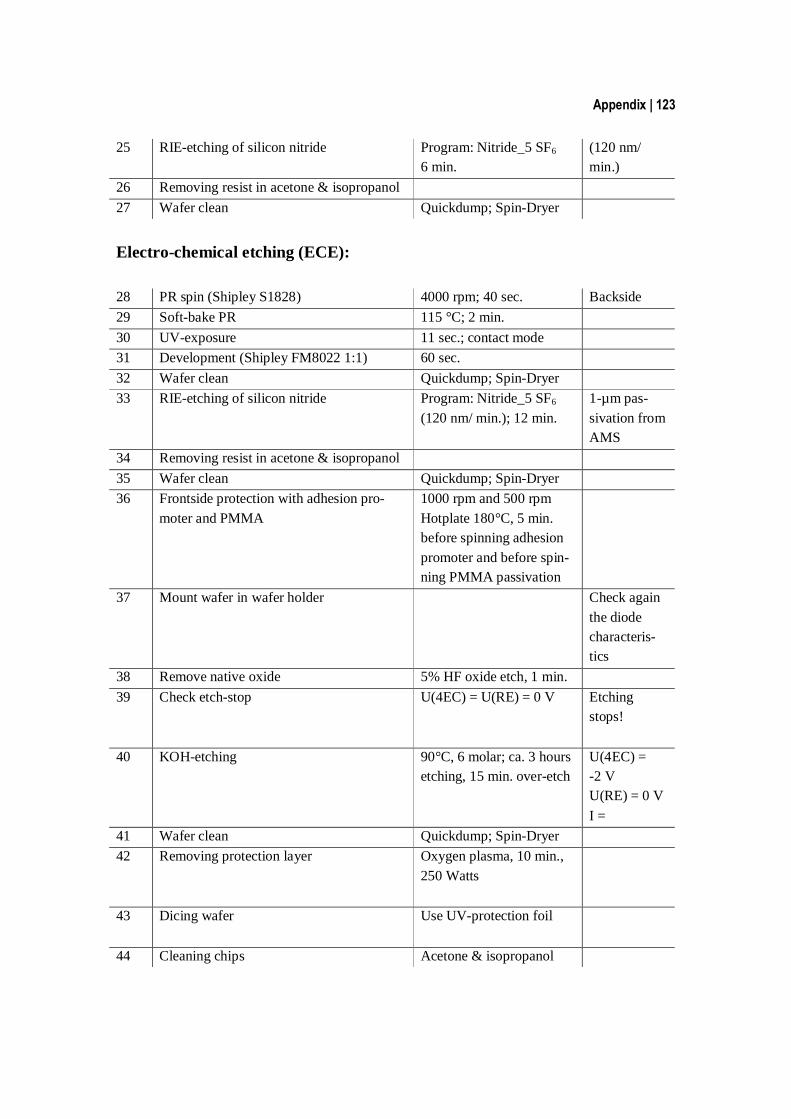
Appendix | 123
25 RIE-etching of silicon nitride
Program: Nitride_5 SF6
6 min. (120 nm/ min.)
26 Removing resist in acetone & isopropanol 27 Wafer clean Quickdump; Spin-Dryer Electro-chemical etching (ECE): 28 PR spin (Shipley S1828) 4000 rpm; 40 sec. Backside 29 Soft-bake PR 115 °C; 2 min. 30 UV-exposure 11 sec.; contact mode 31 Development (Shipley FM8022 1:1) 60 sec. 32 Wafer clean Quickdump; Spin-Dryer 33 RIE-etching of silicon nitride
Program: Nitride_5 SF6 (120 nm/ min.); 12 min.
1-µm pas-sivation from AMS
34 Removing resist in acetone & isopropanol 35 Wafer clean Quickdump; Spin-Dryer 36 Frontside protection with adhesion pro-
moter and PMMA
1000 rpm and 500 rpm Hotplate 180°C, 5 min. before spinning adhesion promoter and before spin-ning PMMA passivation
37 Mount wafer in wafer holder
Check again the diode characteris-tics
38 Remove native oxide 5% HF oxide etch, 1 min. 39 Check etch-stop
U(4EC) = U(RE) = 0 V
Etching stops!
40 KOH-etching
90°C, 6 molar; ca. 3 hours etching, 15 min. over-etch
U(4EC) = -2 V U(RE) = 0 V I =
41 Wafer clean Quickdump; Spin-Dryer 42 Removing protection layer
Oxygen plasma, 10 min., 250 Watts
43 Dicing wafer
Use UV-protection foil
44 Cleaning chips Acetone & isopropanol

124 | Chapter 8
45
Packaging
Bonding; protect bond wires with 10:4 master-bond A & B; mount ring onto the chip to form a cell-culture bath

Appendix | 125
8.2 Staining protocol for neonatal rat cardiomyocytes (NRCs) 1. Remove culture medium 2. Fix cells with 4% paraformaldehyde (PFA) in PBS for 15 min. at room tem-
perature 3. Replace PFA/PBS with 0.1 M glycin in PBS (store at 4°C until use) 4. Rinse with PBS and permeabilize membrane with 0.2% Triton X-100 in PBS
for 10 min. 5. Attach1st antibody:
a. Cardiac myosin-binding protein C using a polyclonal rabbit antibody (polyclonal rabbit, pR anti MyBP-C, COC1, courtesy of M. Gautel)
1:100 in 2 mg/ml BSA/PBS (or in 5% goat serum, 1% BSA in PBS) b. α-actinin protein, Sigma Clone EA53 using monoclonal mouse antibody 1:500 in 2 mg/ml BSA/PBS (or in 5% goat serum, 1% BSA in PBS)
6. Overnight at 4°C or 60 min. at room temperature 7. Rinse 4 x 5 min. with PBS 8. Attach 2nd antibody:
a. Goat-anti-rabbit (GaR) IgG Cy3 (red); 1:500 in 2 mg/ml BSA/PBS
b. Goat-anti-mouse (GaM) IgG Cy5 (blue); 1:200 in 2 mg/ml BSA/PBS
c. Phalloidin Alexa 488 (yellow); 1:100 in 2 mg/ml BSA/PBS
9. 1 hour room temperature (put in aluminum foil) 10. Rinse 3 x 5 min. with PBS 11. Cover sample in Lisbeths Medium, seal & perform microscopy

126 | Chapter 8
8.3 Biocompatibility Experiments Chip preparation: 1. Chips are cleaned in acetone and isopropanol after dicing. 2. Chip coating with the following adhesion proteins and incubated for 2-3
hours, 37°C, 5% CO2: Laminin-1 (10 µg/ml PBS), Sigma L2020 L1Ig6 (10 µg/ml TBS) Poly-L-lysine (PLL) (0.1% in DI-water), Sigma P6282, MW > 70.000 for
30 min. followed by laminin-1 Fibronectin (10 µg/ml PBS), Sigma F1141
3. Additional surface pre-treatment of polydimethylsiloxane (PDMS) chips in oxygen plasma, 1 min., 100 W, before coating. PDMS is used for bio-compatible reasons as it is often used to package and seal the chips.
4. Before placing the neurons, the chips are washed twice with PBS. Dorsal Root Ganglia (DRG): 1. Dorsal root ganglia (DRG) neurons are harvested from 10-day old chicken
embryos. 2. For whole DRGs, the cells are placed immediately after harvesting on the
pre-coated chips. 3. For single cells, the pellet is dissolved in dissociation medium (0.03% colla-
genase A, 0.25% trypsin in MEM) and incubated at 37°C for 35 min. before dissociation.
4. DRG neurons are placed on the chip surface and cultured in EAGLE’s MEM 10% FCS, 5% chick serum and 1 µg/ml nerve growth factor (NGF).
5. Neurons are fixed after 1-, 2- or 4 days in 4% paraformaldehyde (PFA) in TBS for 20 min.
6. For staining experiments, the chips are first washed with TBS and stored in 0.1 M glycin in TBS at 4°C before staining.
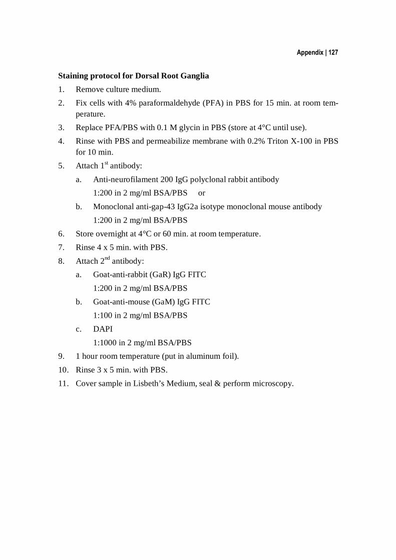
Appendix | 127
Staining protocol for Dorsal Root Ganglia 1. Remove culture medium. 2. Fix cells with 4% paraformaldehyde (PFA) in PBS for 15 min. at room tem-
perature. 3. Replace PFA/PBS with 0.1 M glycin in PBS (store at 4°C until use). 4. Rinse with PBS and permeabilize membrane with 0.2% Triton X-100 in PBS
for 10 min. 5. Attach 1st antibody:
a. Anti-neurofilament 200 IgG polyclonal rabbit antibody 1:200 in 2 mg/ml BSA/PBS or b. Monoclonal anti-gap-43 IgG2a isotype monoclonal mouse antibody 1:200 in 2 mg/ml BSA/PBS
6. Store overnight at 4°C or 60 min. at room temperature. 7. Rinse 4 x 5 min. with PBS. 8. Attach 2nd antibody:
a. Goat-anti-rabbit (GaR) IgG FITC 1:200 in 2 mg/ml BSA/PBS
b. Goat-anti-mouse (GaM) IgG FITC 1:100 in 2 mg/ml BSA/PBS
c. DAPI 1:1000 in 2 mg/ml BSA/PBS
9. 1 hour room temperature (put in aluminum foil). 10. Rinse 3 x 5 min. with PBS. 11. Cover sample in Lisbeth’s Medium, seal & perform microscopy.
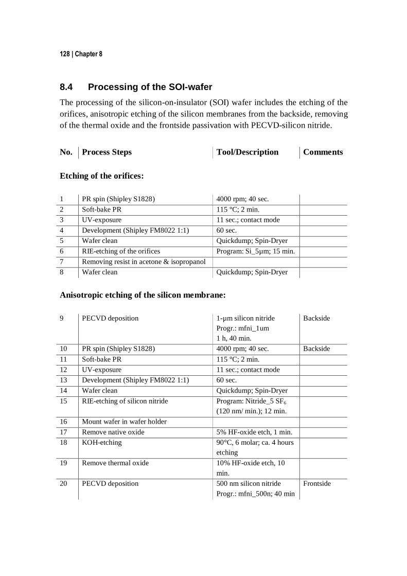
128 | Chapter 8
8.4 Processing of the SOI-wafer The processing of the silicon-on-insulator (SOI) wafer includes the etching of the orifices, anisotropic etching of the silicon membranes from the backside, removing of the thermal oxide and the frontside passivation with PECVD-silicon nitride. No. Process Steps Tool/Description Comments Etching of the orifices: 1 PR spin (Shipley S1828) 4000 rpm; 40 sec. 2 Soft-bake PR 115 °C; 2 min. 3 UV-exposure 11 sec.; contact mode 4 Development (Shipley FM8022 1:1) 60 sec. 5 Wafer clean Quickdump; Spin-Dryer 6 RIE-etching of the orifices Program: Si_5µm; 15 min. 7 Removing resist in acetone & isopropanol 8 Wafer clean Quickdump; Spin-Dryer Anisotropic etching of the silicon membrane: 9 PECVD deposition 1-µm silicon nitride
Progr.: mfni_1um 1 h, 40 min.
Backside
10 PR spin (Shipley S1828) 4000 rpm; 40 sec. Backside 11 Soft-bake PR 115 °C; 2 min. 12 UV-exposure 11 sec.; contact mode 13 Development (Shipley FM8022 1:1) 60 sec. 14 Wafer clean Quickdump; Spin-Dryer 15 RIE-etching of silicon nitride
Program: Nitride_5 SF6 (120 nm/ min.); 12 min.
16 Mount wafer in wafer holder 17 Remove native oxide 5% HF-oxide etch, 1 min. 18 KOH-etching 90°C, 6 molar; ca. 4 hours
etching
19 Remove thermal oxide 10% HF-oxide etch, 10 min.
20 PECVD deposition 500 nm silicon nitride Progr.: mfni_500n; 40 min
Frontside

Appendix | 129
21 Dicing wafer Use UV-protection foil 22 Cleaning chips Acetone & isopropanol 23 Packaging

130 | Chapter 8
8.5 Fabrication steps of the microfluidic chip No. Process Steps Tool/Description Comments SU-8 master for PDMS: 1 Dehydration (silicon wafer) Hotplate; 180°C, 60 min 2 PR spin (Microchem SU-8 50)
- 500 rpm; 10 sec. then ramp to - 1250 rpm; 40 sec. (for 100 µm high structures)
3 Soft-bake PR
- 65°C for 1 min. then ramp to 100°C for 75 min.
- Cool wafer down slowly for 60 min.
4 UV-exposure
- Contact mode 5/10 N - Separation 99 µm - Mask thickness 2.5 mm - Exposure time 70 sec. (600 mJ/cm2)
5 Post exposure bake
1. 65°C for 1 min. 95°C for 45 min. 2. Cool wafer down slowly for 60 min.
PDMS molding: 8 SU-8 master preparation
Pre-treatment of wafer
Washing master with 0.05% Triton-X Let master dry
Prevents the irreversible attachment of the master to the PDMS
9 PDMS mixing
Mix 10:1 wt of Sylgard 184 (A and B) in plastic cup
10 Degassing PDMS Place cup in vacuum for degassing for 30 min.

Appendix | 131
11 Curing PDMS
- pour PDMS on wafer (ca. 3 mm) - curing on hotplate; 70°C, 4 hours
12 Relieving
Peel carefully the PDMS layer off the wafer

132 | Chapter 8
8.6 Cell-screening experiments using normal human dermal fibroblasts (NHDFs)
Splitting of the NHDFs
1. Remove culture medium. 2. Wash cells with sterile PBS. 3. Add 0.25% trypsin in MEM, Petri dish (2 ml) or well (200 µl), place dish in
incubator for 3 min. 4. Check under microscope if cells are detached. 5. Terminate the reaction with DMEM 10% FCS (3 times the amount of tryp-
sin). 6. Fill the content in 15 ml falcon tube and centrifuge at 1500 rpm, 3 min. 7. Remove the supernatant. 8. Add a few milliliters DMEM 10% FCS. 9. Place the cells in the desired wells or Petri dishes, add more medium. Life/Dead staining
1. Remove culture medium. 2. Wash cells 2× with PBS. 3. Prepare stock solutions: Fluorescein-diacetat: 2.5 mg/ml DMSO Ethidium bromide: 10 mg/ml DI-water 4. Add 1 µl of each stock solution in 1 ml PBS. 5. Fill working solution into wells; incubate for 30-60 sec. 6. Remove working solution and wash 2× with PBS Ethanol drug screening experiment
1. Remove medium. 2. Wash 1× with PBS. 3. Fill the different ethanol concentrations in 10% FCS medium. 4. Incubate for 30 min, 60 min, 90 min.

Appendix | 133
5. Remove ethanol, wash 2× with PBS. 6. Life/Dead staining.
Cell tracker experiment
1. Prepare 10 mM stock solution: 1 mg cell tracker (C2925); MW 464.86 g; dis-solve 215 µl DMSO in 1 mg cell tracker.
2. Grow cells in wells, let them adhere over night. 3. Remove the medium from the wells. 4. Add the pre-warmed working concentration of cell tracker (1-100 µM) in se-
rum-free medium. 5. Incubate at 37°C for 15-45 min. 6. Replace the working solution with culture medium, incubate for another 30
min. at 37°C. 7. Wash cells with PBS. 8. Add culture medium or fix cells with PFA.


Acknowledgements | 135
9 Acknowledgements Over the last five years, Prof. Andreas Hierlemann has built an excellent research team in the emerging field of bio-electronics. I am indebted for the years that I could spend in this stimulating environment to work towards my PhD. I appreci-ated Andreas’ discreet style of supervision that left room for my own decisions and visions. Still, he always had an open door for professional as well as personal discussions. Andreas, I was always impressed how you could turn my humble se-quence of English words into a sophisticated report. When I arrived in Zurich in 1999, one of the first lectures I visited was in ‘Mi-crosensors’ given by Prof. Henry Baltes. I was really fascinated about his enthusi-astic style of teaching and the pleasure Henry had in semiconductor technology. Later on I had the chance to work part-time in his lab which not only allowed me financing the life in Zurich, but also gave me hands-on experience in the world of research. I am grateful that you gave me the opportunity to go to Waterloo for my diploma thesis and that you made me return to do my PhD at PEL. Before I started my PhD thesis, I had never touched a pipette or had been in a mi-crobiology laboratory. Everything I learned about culturing cells, I was taught by my second supervisor PD Dr. Heike Hall. Thank you, Heike, for your patience and effort to teach me and also for your great interest in the more applied areas of bi-ology.
I also gratefully acknowledge Prof. Milena Koudelka-Hep from the Institute of Microtechnology in Neuchâtel for kindly agreeing to be the co-examiner of my thesis.
Bio-electronics is a highly interdisciplinary field, which requires people with all different kinds of background and interests to be fruitful. This is exactly what we have at PEL, and I would like to address special thanks to my colleagues from the bio-electronic group Flavio Heer, Sadik Hafizovic, Urs Frey, Kay-Uwe Kirstein, and Wendy Franks. Each of them contributed a lot to my thesis with enthusiastic discussions and helpful advice. I am especially grateful to Urs for providing the

136 | Chapter 9
external circuitry for my bio-electronic chip and to Kay-Uwe for being the best, most patient and supportive leader of the microelectronics team I could imagine. It was really a pleasure to work with you.
During my PhD thesis I had the opportunity to work with a number of semester and diploma students. Nima Riahi joined me to develop a protocol for the lift-off process. Stefan Rosanelli developed a new package for the bio-electronic chip and Livia Seemann did a great job in designing a cascading microfluidic cover for im-mobilized, incubated cells.
Under the best conditions, a working relationship can turn into friendship. Sonja Bonneick and Jens Kelm are a good example for a friendship that started in an ETH-internal project. Thanks for all the biological advice and the pleasure to work together.
The recording of electrogenic cells with the bio-electronic chip would have been impossible without the help of Evelyne and Prof. Jean-Claude Perriard from the Institute of Cell Biology. I am very grateful to them for providing neonatal rat car-diomyocytes for my experiments and very helpful culturing and staining advice.
Anne Greet Bittermann and Ursula Lüthi from the EMZ are kindly acknowledged for the great SEM and TEM images. Their technical skills and professional han-dling of these complex instruments were amazing.
Markus Graf, Petra Kurzawski, Adrian Kummer are also gratefully acknowledged for creating a pleasant and sometimes wet biotope in our office with integrated bar service. Our relationship goes far beyond being office mates. Thanks for the great time together that was complemented by several enjoyable semester and diploma students over the years: Marko Mihailovic, René Tölke, Ivan Schenker, Claudia Küttel, Rene Pedron and Jürg Müller.
A warm thanks goes to the institute’s support staff at PEL: Erna Hug and Yelena von Allmen for managing the administrative parts and being the ‘souls’ of PEL, Chris Kolb and Igor Levak for the computer support and last but not least Donat Scheiwiller for maintaining the lab equipment and for all the technical advice to improve my processing. The great atmosphere at PEL would not have been the same without the rest of the group: Nils Gödecke, Jan Lichtenberg, Cyril Vancura, Tobias Vancura, Tomi Salo, Diego Barrettino, Nicole Kerness, Wan Ho Song, Robert Sunier, Yue Li, Tormod Volden, Martin Zimmermann, Stefano Taschini, Christoph Hagleitner, Branka Roscic, and Timo the dog.

Acknowledgements | 137
All the work, the long years of studies and educational training would not have been possible without the help of my parents. It was their love and faith that helped me to be where I am now.
Last but not least, I would like to express my sincere gratitude to Jan, the one spe-cial person in my life who has so many qualities. I am so grateful for all your tech-nical advice, your endless support over the years, your motivation upon the occur-rence of challenges, your love and friendship. Thank you for always being there.


Publications | 139
10 Publications Journal Papers F. Greve, A. Hierlemann, H. Baltes, H. Hall, ‘Neuron guidance on bio-
electronic chip’. European cells and materials, vol. 6 suppl. 1, 2003 (page 91). J. M. Kelm, V. Djonov, S. P. Hoerstrup, C. I. Guenter, L. M. Ittner, F. Greve,
A. Hierlemann, C. Diaz Sanchez-Bustamante, J.-C. Perriard, E. Ehler, M. Fussenegger, ‘Tissue-transplant fusion and vascularization of myocardial mi-cro- and macrotissues implanted into chicken embryos and rats’. Tissue Engi-neering, in press.
F. Greve, J. Lichtenberg, K.-U. Kirstein, U. Frey, J.-C. Perriard, A. Hierlemann ‘Perforated CMOS microchip for immobilization and activity monitoring of electrogenic cells’. Manuscript in preparation.
F. Greve, L. Seemann, A. Hierlemann, J. Lichtenberg, ‘High-throughput cell-based screening system with on-chip dilution stage’. Manuscript in preparation.
Conference contributions F. Greve, A. Hierlemann, H. Baltes, H. Hall, ‘Towards defined neuronal net-
works on bio-electronic chips’. Biosurf IV 2003, Zurich, Switzerland. F. Greve, J. Lichtenberg, A. Hierlemann, H. Baltes, ‘Physical neuron immobi-
lization on electrode arrays by mild suction’. SmallTalk 2003, San Jose, USA. F. Greve, J. Lichtenberg, H. Hall, A. Hierlemann, H. Baltes, ‘Physical immobi-
lization and polymeric microchannel networks to achieve defined neuronal network structures. µTAS 2003, Lake Tahoe, USA.
F. Greve, A. Hierlemann, H. Baltes, H. Hall, ‘Neuronal cell growth on bio-electronic chips’. ZNZ Symopsium 2003, Zurich, Switzerland.
F. Greve, J. Lichtenberg, H. Hall, A. Hierlemann, ‘Microfluidic PDMS channel system to achieve defined neuronal network topologies for electrical activity measurements’. Biosensors 2004, Granada, Spain.
140 | Chapter 10
F. Greve, J. Lichtenberg, A. Hierlemann, H. Baltes, ’Precise cell placement by pneumatic anchoring’. IEEE Sensors 2004, Vienna, Austria.
F. Heer; W. Franks, A. Blau, S. Hafizovics, F. Greve; S. Taschini, C. Ziegler, A. Hierlemann, H. Baltes, ‘CMOS microchip for recording and stimulation of electrogenic cells’. MEA Meeting 2004, Reutlingen, Germany.
F. Greve, J. Lichtenberg, K.-U. Kirstein, U. Frey, A. Hierlemann, ‘Perforated CMOS microchip as platform for immobilization and activity monitoring of electrogenic cells’. Transducers 2005, Seoul, South Korea.
S. Hafizovic, F. Heer, W. Franks, A. Blau, C. Ziegler, A. Hierlemann, ‘CMOS Bidirectional Electrode Array for Electrogenic Cells’. MEMS 2006, Istanbul, Turkey.
Patents F. Greve, L. Seemann, J. Lichtenberg, ‘High-throughput cell-based screening
system with on-chip dilution stage’, patent application pending.

Curriculum Vitae | 141
11 Curriculum Vitae Frauke Greve Born, July 26, 1973 Citizen of Germany
July 2002 – March 2006 Work on Ph.D. thesis entitled ‘Micromachined plat-forms for manipulating and recording from cells’ at the Physical Electronic Laboratory, ETH Zurich, Switzerland, supervised by Prof. Dr. Andreas Hierle-mann.
Oct. 2001 – March 2002 Diploma thesis entitled ‘Patterning techniques for the fabrication of polymer electronics’ at the University of Waterloo, Canada, supervised by Prof. Dr. Arokia Nathan.
Oct. 1999 – April 2002 Student of Electrical Engineering at the ETH Zurich. Sept. 1998 – July 1999 Exchange student at the University of Plymouth,
Great Britain. Oct. 1996 – July 1998 Undergraduate student of Electrical Engineering at
the University Bremen, Germany. July 1995 – Oct. 1996 Technical assistant at the Institute of Sensors, Actua-
tors and Systems (IMSAS), University of Bremen, Germany. Responsible for wet chemical etching tech-niques and scanning electron microscopy.
Aug. 1993 – June 1995 Accredited two-year vocational program at the ‘School for Physical Technical Assistants’, Bremen. Title: Physical technical assistant.
June 1993 Abitur (German school leaving certificate) at the Gymnasium Antonianum Vechta, Germany.