rf power transistor, ldmost plastic family n … 2010 doc id 11758 rev 4 1/21 21 pd57060s-e rf power...
TRANSCRIPT
June 2010 Doc ID 11758 Rev 4 1/21
21
PD57060S-ERF POWER transistor, LdmoST plastic family
N-channel enhancement-mode, lateral MOSFETs
Features■ Excellent thermal stability
■ Common source configuration
■ POUT = 60 W with 14.3dB gain@ 945 MHz/28 V
■ New RF plastic package
DescriptionThe device is a common source N-channel, enhancement-mode lateral field-effect RF power MOSFET. It is designed for high gain, broad band commercial and industrial applications. It operates at 28 V in common source mode at frequencies up to 1 GHz. The device boasts the excellent gain, linearity and reliability of ST’s latest LDMOS technology mounted in the first true SMD plastic RF power package, PowerSO-10RF. Device’s superior linearity performance makes it an ideal solution for base station applications. The PowerSO-10 plastic package, designed to offer high reliability, is the first ST JEDEC approved, high power SMD package. It has been specially optmized for RF needs and offers excellent RF performances and ease of assembly. Mounting recommendations are available in www.st.com/rf/ (look for application note AN1294).
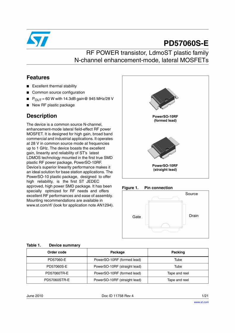
Figure 1. Pin connection
PowerSO-10RF(formed lead)
PowerSO-10RF(straight lead)
Gate
Source
Drain
Table 1. Device summary
Order code Package Packing
PD57060-E PowerSO-10RF (formed lead) Tube
PD57060S-E PowerSO-10RF (straight lead) Tube
PD57060TR-E PowerSO-10RF (formed lead) Tape and reel
PD57060STR-E PowerSO-10RF (straight lead) Tape and reel
www.st.com

Contents PD57060-E
2/21 Doc ID 11758 Rev 4
Contents
1 Electrical data . . . . . . . . . . . . . . . . . . . . . . . . . . . . . . . . . . . . . . . . . . . . . . 3
1.1 Maximum ratings . . . . . . . . . . . . . . . . . . . . . . . . . . . . . . . . . . . . . . . . . . . . 3
1.2 Thermal data . . . . . . . . . . . . . . . . . . . . . . . . . . . . . . . . . . . . . . . . . . . . . . . 3
2 Electrical characteristics . . . . . . . . . . . . . . . . . . . . . . . . . . . . . . . . . . . . . 4
2.1 Static . . . . . . . . . . . . . . . . . . . . . . . . . . . . . . . . . . . . . . . . . . . . . . . . . . . . . 4
2.2 Dynamic . . . . . . . . . . . . . . . . . . . . . . . . . . . . . . . . . . . . . . . . . . . . . . . . . . . 4
2.3 Moisture sensitivity level . . . . . . . . . . . . . . . . . . . . . . . . . . . . . . . . . . . . . . . 4
3 Impedances . . . . . . . . . . . . . . . . . . . . . . . . . . . . . . . . . . . . . . . . . . . . . . . . 5
4 Typical performance . . . . . . . . . . . . . . . . . . . . . . . . . . . . . . . . . . . . . . . . . 6
5 Test circuit . . . . . . . . . . . . . . . . . . . . . . . . . . . . . . . . . . . . . . . . . . . . . . . . . 9
6 Common source s-parameter . . . . . . . . . . . . . . . . . . . . . . . . . . . . . . . . 12
7 Package mechanical data . . . . . . . . . . . . . . . . . . . . . . . . . . . . . . . . . . . . 15
8 Revision history . . . . . . . . . . . . . . . . . . . . . . . . . . . . . . . . . . . . . . . . . . . 20
PD57060-E Electrical data
Doc ID 11758 Rev 4 3/21
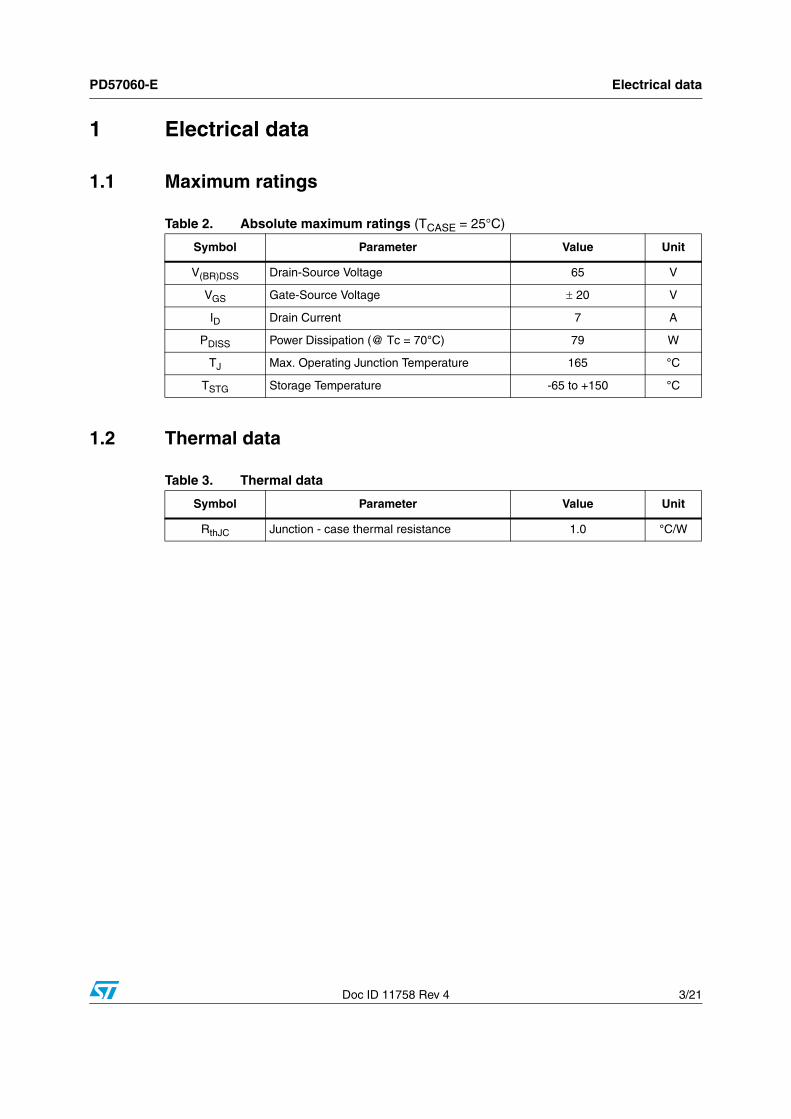
1 Electrical data
1.1 Maximum ratings
1.2 Thermal data
Table 2. Absolute maximum ratings (TCASE = 25°C)
Symbol Parameter Value Unit
V(BR)DSS Drain-Source Voltage 65 V
VGS Gate-Source Voltage ± 20 V
ID Drain Current 7 A
PDISS Power Dissipation (@ Tc = 70°C) 79 W
TJ Max. Operating Junction Temperature 165 °C
TSTG Storage Temperature -65 to +150 °C
Table 3. Thermal data
Symbol Parameter Value Unit
RthJC Junction - case thermal resistance 1.0 °C/W

Electrical characteristics PD57060-E
4/21 Doc ID 11758 Rev 4
2 Electrical characteristics
TCASE = +25 oC
2.1 Static
2.2 Dynamic
2.3 Moisture sensitivity level
Table 4. Static
Symbol Test conditions Min Typ Max Unit
V(BR)DSS VGS = 0 IDS = 1 mA 65 V
IDSS VGS = 0 VDS = 28 V 1 µA
IGSS VGS = 20 V VDS = 0 V 1 µA
VGS(Q) VDS = 28 V ID = 100 mA 2.0 4.0 V
VDS(ON) VGS = 10 V ID = 3 A 0.7 0.8 V
GFS VDS = 10 V ID = 3 A 2.5 mho
CISS VGS = 0 VDS = 28 V f = 1 MHz 83 pF
COSS VGS = 0 VDS = 28 V f = 1 MHz 58 pF
CRSS VGS = 0 VDS = 28 V f = 1 MHz 3 pF
Table 5. Dynamic
Symbol Test conditions Min Typ Max Unit
POUT VDD = 28 V IDQ = 100 mA f = 945MHz 60 W
GPS VDD = 28 V IDQ = 100 mA POUT = 60 W f = 945MHz 14.3 dB
ηD VDD = 28 V IDQ = 100 mA POUT = 60 W f = 945MHz 54 %
Load Mismatch
VDD = 28 V IDQ = 100 mA POUT = 60W f = 945MHz
All Phase Angles5:1 VSWR
Table 6. Moisture sensitivity level
Test methodology Rating
J-STD-020B MSL 3
PD57060-E Impedances
Doc ID 11758 Rev 4 5/21
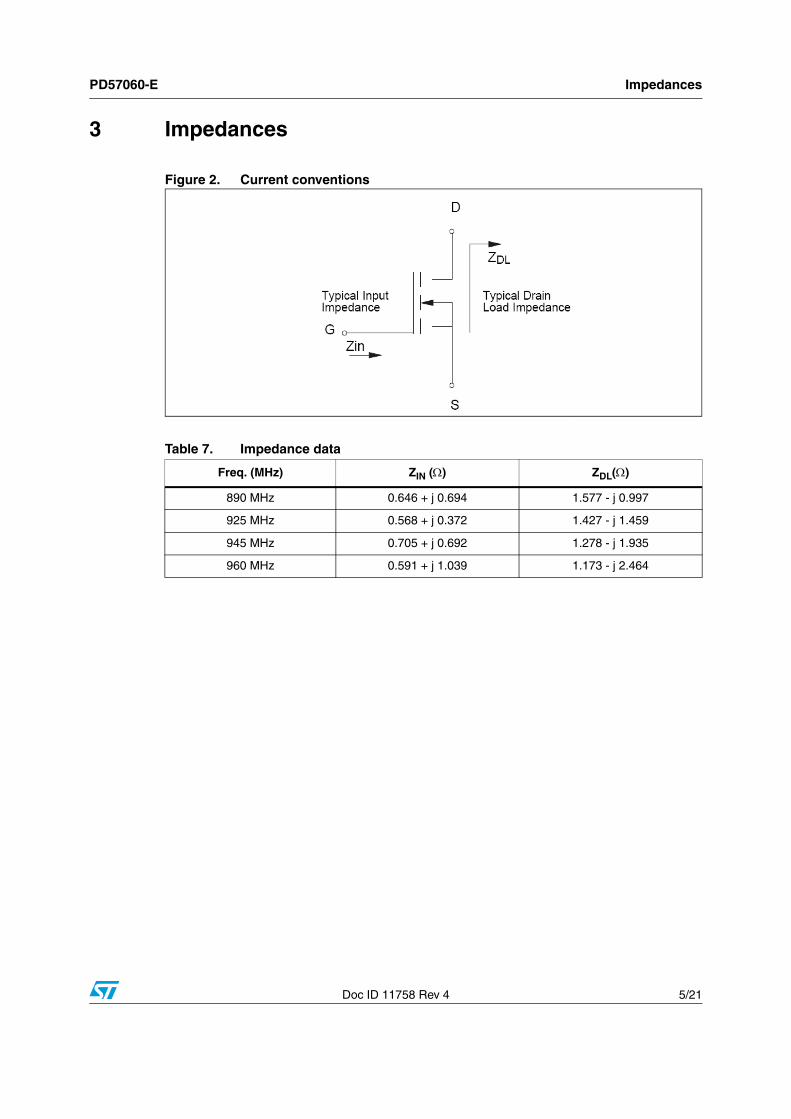
3 Impedances
Figure 2. Current conventions
Table 7. Impedance data
Freq. (MHz) ZIN (Ω) ZDL(Ω)
890 MHz 0.646 + j 0.694 1.577 - j 0.997
925 MHz 0.568 + j 0.372 1.427 - j 1.459
945 MHz 0.705 + j 0.692 1.278 - j 1.935
960 MHz 0.591 + j 1.039 1.173 - j 2.464
Typical performance PD57060-E
6/21 Doc ID 11758 Rev 4
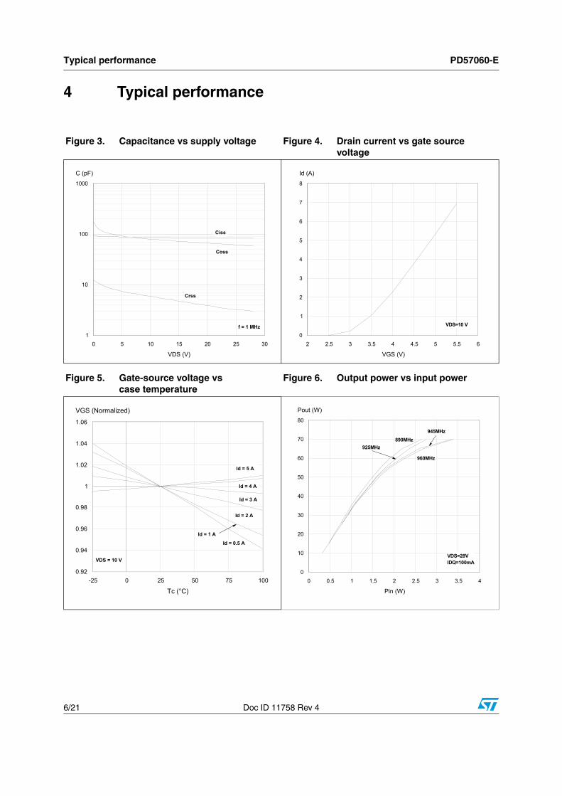
4 Typical performance
Figure 3. Capacitance vs supply voltage Figure 4. Drain current vs gate source voltage
Figure 5. Gate-source voltage vscase temperature
Figure 6. Output power vs input power
0 5 10 15 20 25 30
VDS (V)
1
10
100
1000
C (pF)
f = 1 MHz
Crss
Ciss
Coss
2 2.5 3 3.5 4 4.5 5 5.5 6
VGS (V)
0
1
2
3
4
5
6
7
8
Id (A)
VDS=10 V
-25 0 25 50 75 100
Tc (°C)
0.92
0.94
0.96
0.98
1
1.02
1.04
1.06
VGS (Normalized)
VDS = 10 V
Id = 0.5 A
Id = 1 A
Id = 2 A
Id = 3 A
Id = 4 A
Id = 5 A
0 0.5 1 1.5 2 2.5 3 3.5 4
Pin (W)
0
10
20
30
40
50
60
70
80
Pout (W)
VDS=28VIDQ=100mA
960MHz
945MHz890MHz
925MHz
PD57060-E Typical performance
Doc ID 11758 Rev 4 7/21
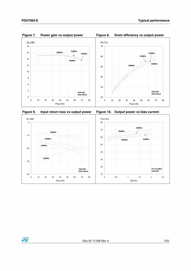
Figure 7. Power gain vs output power Figure 8. Drain efficiency vs output power
Figure 9. Input return loss vs output power Figure 10. Output power vs bias current
0 10 20 30 40 50 60 70 80
Pout (W)
2
4
6
8
10
12
14
16
18
Gp (dB)
VDS=28VIDQ=100mA
960MHz
945MHz890MHz
925MHz
0 10 20 30 40 50 60 70 80
Pout (W)
20
30
40
50
60
70
Nd (%)
VDS=28VIDQ=100mA
960MHz890MHz
945MHz925MHz
0 10 20 30 40 50 60 70 80
Pout (W)
-40
-30
-20
-10
0
RL (dB)
VDS=28VIDQ=100mA
945MHz
925MHz
960MHz
890MHz
0 0.5 1 1.5 2 2.5
IDQ (A)
10
20
30
40
50
60
70
80
Pout (W)
Pin=32.8dBmVDS=28V
960MHz
890MHz
945MHz
925MHz

Typical performance PD57060-E
8/21 Doc ID 11758 Rev 4
Figure 11. Drain efficiency vs bias current Figure 12. Output power vs supply voltage
Figure 13. Drain efficiency vs supply voltage Figure 14. Output power vs gate-source voltage
0 0.5 1 1.5 2 2.5
IDQ (A)
10
20
30
40
50
60
70
Nd (%)
Pin=32.8dBmVDS=28V
960MHz925MHz
890MHz 945MHz
10 15 20 25 30
VDS (V)
10
20
30
40
50
60
70
Pout (W)
Pin=32.8dBmIDQ=100mA
960MHz
890MHz
925MHz
945MHz
10 15 20 25 30
VDS (V)
10
20
30
40
50
60
70
Nd (%)
Pin=32.8dBmIDQ=100mA
960MHz925MHz
890MHz 945MHz
0 1 2 3 4 5
VGS (V)
10
20
30
40
50
60
70
80
Pout (W)
Pin=32.8dBmVDS=28v
960MHz
9455MHz
890MHz
925MHz
PD57060-E Test circuit
Doc ID 11758 Rev 4 9/21
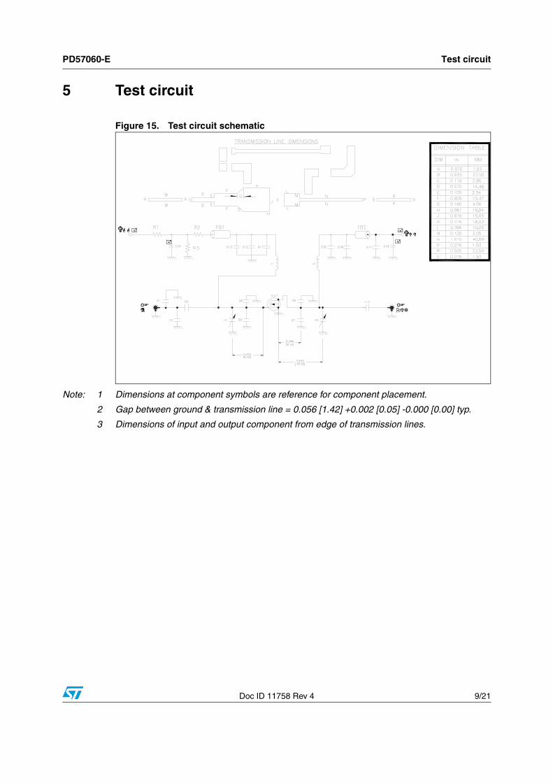
5 Test circuit
Figure 15. Test circuit schematic
Note: 1 Dimensions at component symbols are reference for component placement.
2 Gap between ground & transmission line = 0.056 [1.42] +0.002 [0.05] -0.000 [0.00] typ.
3 Dimensions of input and output component from edge of transmission lines.
Test circuit PD57060-E
10/21 Doc ID 11758 Rev 4
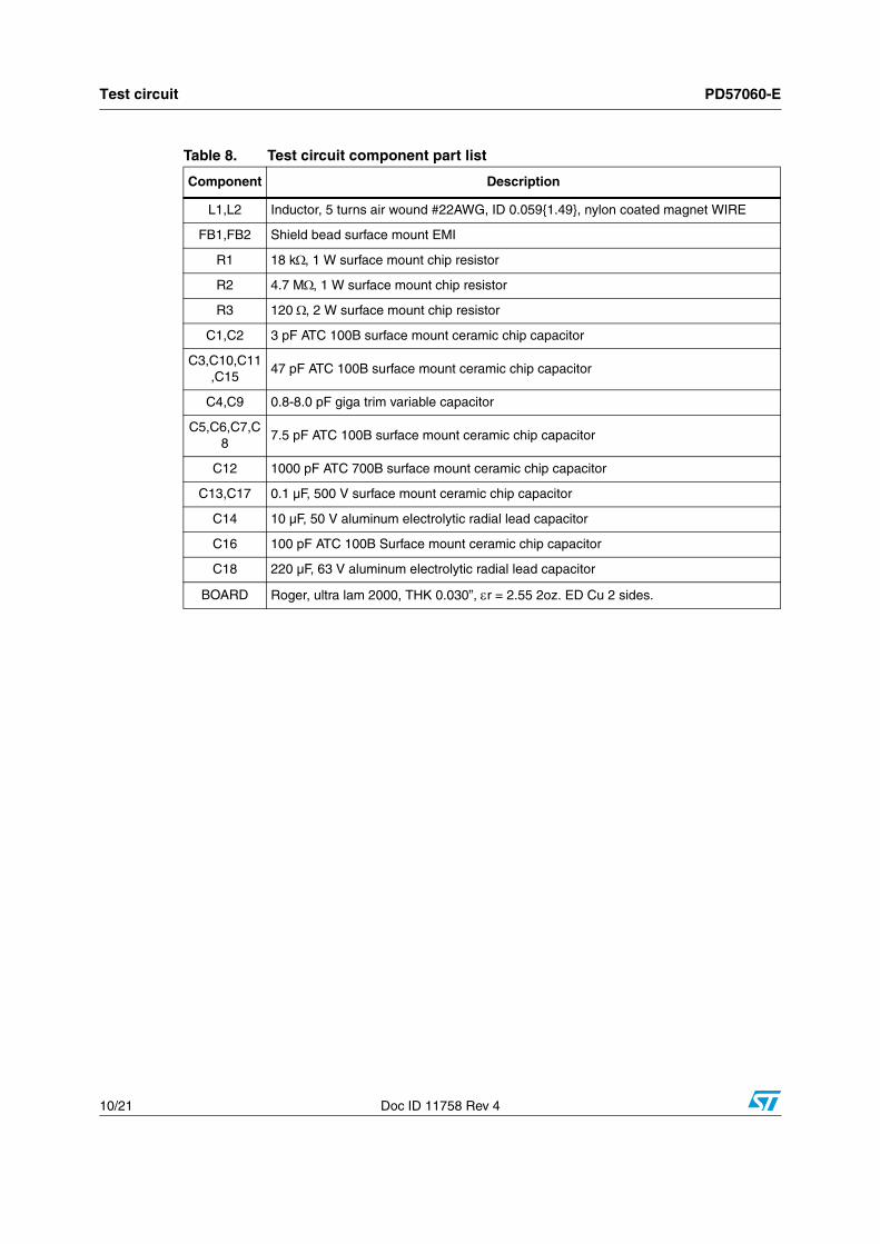
Table 8. Test circuit component part list
Component Description
L1,L2 Inductor, 5 turns air wound #22AWG, ID 0.059{1.49}, nylon coated magnet WIRE
FB1,FB2 Shield bead surface mount EMI
R1 18 kΩ, 1 W surface mount chip resistor
R2 4.7 MΩ, 1 W surface mount chip resistor
R3 120 Ω, 2 W surface mount chip resistor
C1,C2 3 pF ATC 100B surface mount ceramic chip capacitor
C3,C10,C11,C15
47 pF ATC 100B surface mount ceramic chip capacitor
C4,C9 0.8-8.0 pF giga trim variable capacitor
C5,C6,C7,C8
7.5 pF ATC 100B surface mount ceramic chip capacitor
C12 1000 pF ATC 700B surface mount ceramic chip capacitor
C13,C17 0.1 µF, 500 V surface mount ceramic chip capacitor
C14 10 µF, 50 V aluminum electrolytic radial lead capacitor
C16 100 pF ATC 100B Surface mount ceramic chip capacitor
C18 220 µF, 63 V aluminum electrolytic radial lead capacitor
BOARD Roger, ultra lam 2000, THK 0.030”, εr = 2.55 2oz. ED Cu 2 sides.

PD57060-E Test circuit
Doc ID 11758 Rev 4 11/21
Figure 16. Test circuit
Figure 17. Test circuit photomaster
6.4 inches
4 in
ches
PD57060
Common source s-parameter PD57060-E
12/21 Doc ID 11758 Rev 4
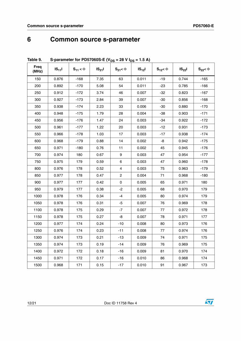
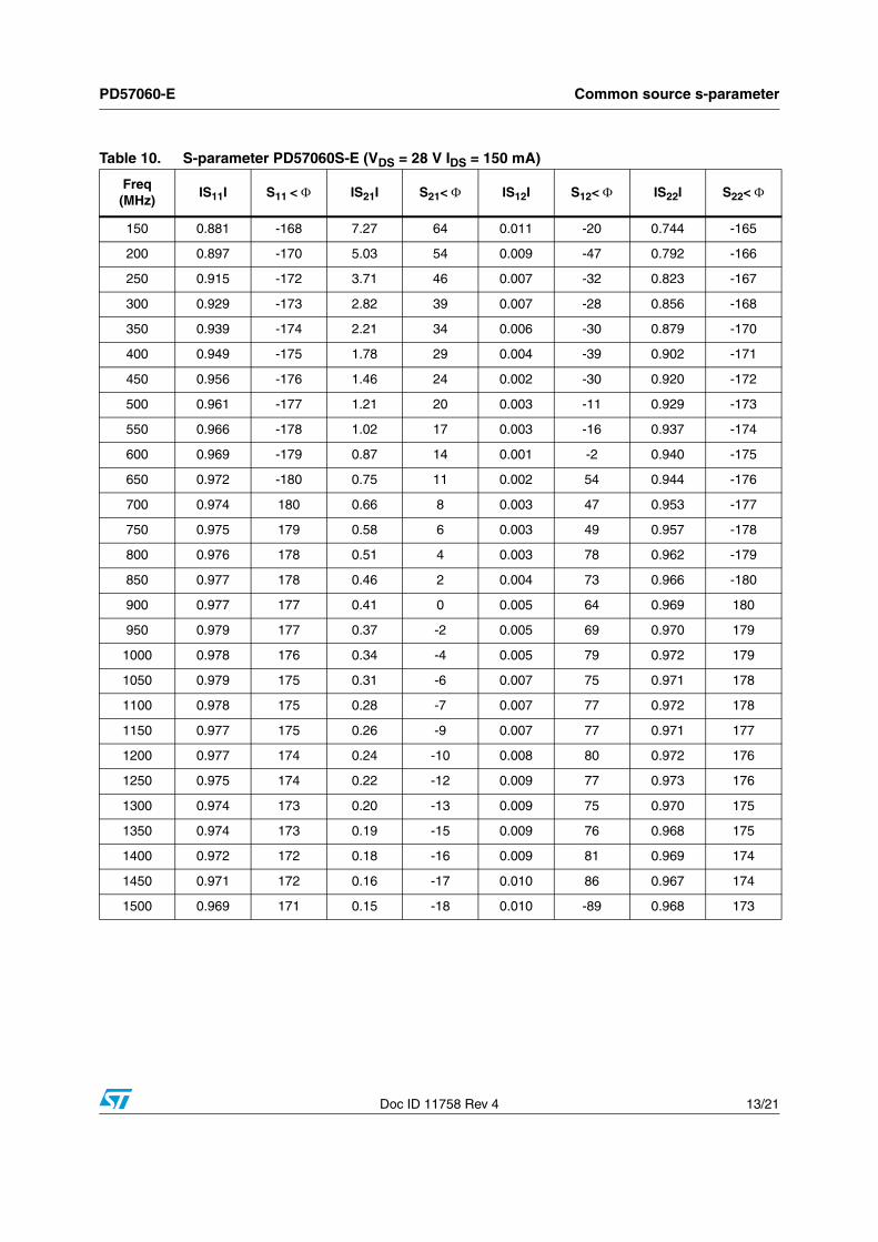
6 Common source s-parameter
Table 9. S-parameter for PD57060S-E (VDS = 28 V IDS = 1.5 A)
Freq (MHz)
IS11I S11 < Φ IS21I S21< Φ IS12I S12< Φ IS22I S22< Φ
150 0.876 -168 7.35 63 0.011 -19 0.744 -165
200 0.892 -170 5.08 54 0.011 -23 0.785 -166
250 0.912 -172 3.74 46 0.007 -32 0.823 -167
300 0.927 -173 2.84 39 0.007 -30 0.856 -168
350 0.938 -174 2.23 33 0.006 -30 0.880 -170
400 0.948 -175 1.79 28 0.004 -38 0.903 -171
450 0.956 -176 1.47 24 0.003 -34 0.922 -172
500 0.961 -177 1.22 20 0.003 -12 0.931 -173
550 0.966 -178 1.03 17 0.003 -17 0.938 -174
600 0.968 -179 0.88 14 0.002 -8 0.942 -175
650 0.971 -180 0.76 11 0.002 45 0.945 -176
700 0.974 180 0.67 9 0.003 47 0.954 -177
750 0.975 179 0.59 6 0.003 47 0.960 -178
800 0.976 178 0.52 4 0.003 75 0.963 -179
850 0.977 178 0.47 2 0.004 71 0.968 -180
900 0.977 177 0.42 0 0.005 65 0.971 180
950 0.979 177 0.38 -2 0.005 68 0.970 179
1000 0.978 176 0.34 -4 0.005 80 0.974 179
1050 0.978 176 0.31 -5 0.007 76 0.969 178
1100 0.978 175 0.29 -7 0.007 77 0.972 178
1150 0.978 175 0.27 -8 0.007 78 0.971 177
1200 0.977 174 0.24 -10 0.008 80 0.973 176
1250 0.976 174 0.23 -11 0.008 77 0.974 176
1300 0.974 173 0.21 -13 0.009 74 0.971 175
1350 0.974 173 0.19 -14 0.009 76 0.969 175
1400 0.972 172 0.18 -16 0.009 81 0.970 174
1450 0.971 172 0.17 -16 0.010 86 0.968 174
1500 0.968 171 0.15 -17 0.010 91 0.967 173
PD57060-E Common source s-parameter
Doc ID 11758 Rev 4 13/21
Table 10. S-parameter PD57060S-E (VDS = 28 V IDS = 150 mA)
Freq (MHz)
IS11I S11 < Φ IS21I S21< Φ IS12I S12< Φ IS22I S22< Φ
150 0.881 -168 7.27 64 0.011 -20 0.744 -165
200 0.897 -170 5.03 54 0.009 -47 0.792 -166
250 0.915 -172 3.71 46 0.007 -32 0.823 -167
300 0.929 -173 2.82 39 0.007 -28 0.856 -168
350 0.939 -174 2.21 34 0.006 -30 0.879 -170
400 0.949 -175 1.78 29 0.004 -39 0.902 -171
450 0.956 -176 1.46 24 0.002 -30 0.920 -172
500 0.961 -177 1.21 20 0.003 -11 0.929 -173
550 0.966 -178 1.02 17 0.003 -16 0.937 -174
600 0.969 -179 0.87 14 0.001 -2 0.940 -175
650 0.972 -180 0.75 11 0.002 54 0.944 -176
700 0.974 180 0.66 8 0.003 47 0.953 -177
750 0.975 179 0.58 6 0.003 49 0.957 -178
800 0.976 178 0.51 4 0.003 78 0.962 -179
850 0.977 178 0.46 2 0.004 73 0.966 -180
900 0.977 177 0.41 0 0.005 64 0.969 180
950 0.979 177 0.37 -2 0.005 69 0.970 179
1000 0.978 176 0.34 -4 0.005 79 0.972 179
1050 0.979 175 0.31 -6 0.007 75 0.971 178
1100 0.978 175 0.28 -7 0.007 77 0.972 178
1150 0.977 175 0.26 -9 0.007 77 0.971 177
1200 0.977 174 0.24 -10 0.008 80 0.972 176
1250 0.975 174 0.22 -12 0.009 77 0.973 176
1300 0.974 173 0.20 -13 0.009 75 0.970 175
1350 0.974 173 0.19 -15 0.009 76 0.968 175
1400 0.972 172 0.18 -16 0.009 81 0.969 174
1450 0.971 172 0.16 -17 0.010 86 0.967 174
1500 0.969 171 0.15 -18 0.010 -89 0.968 173

Common source s-parameter PD57060-E
14/21 Doc ID 11758 Rev 4
Table 11. S-parameter for PD57060S-E (VDS = 13.5 V IDS = 75 mA)
Freq (MHz)
IS11I S11 < Φ IS21I S21< Φ IS12I S12< Φ IS22I S22< Φ
150 0.880 -173 4.67 69 0.012 -17 0.829 -174
200 0.891 -173 3.36 61 0.013 -33 0.848 -174
250 0.904 -175 2.54 55 0.010 -26 0.868 -175
300 0.915 -175 1.99 49 0.009 -20 0.881 -175
350 0.924 -176 1.61 43 0.009 -28 0.894 -176
400 0.933 -177 1.32 38 0.007 -36 0.909 -176
450 0.940 -177 1.10 34 0.005 -27 0.915 -177
500 0.946 -178 0.93 30 0.005 -24 0.926 -178
550 0.953 -179 0.80 27 0.005 -28 0.937 -178
600 0.956 -179 0.69 23 0.004 -24 0.942 -179
650 0.961 -180 0.61 20 0.003 -5 0.949 -180
700 0.964 179 0.53 18 0.004 10 0.954 180
750 0.966 179 0.48 15 0.003 4 0.955 179
800 0.967 178 0.43 13 0.002 43 0.960 178
850 0.968 178 0.38 11 0.004 51 0.956 178
900 0.971 177 0.35 9 0.004 43 0.962 177
950 0.971 177 0.32 7 0.004 55 0.966 176
1000 0.971 176 0.29 5 0.004 70 0.968 176
1050 0.975 175 0.26 4 0.006 68 0.971 175
1100 0.973 175 0.24 2 0.006 63 0.970 175
1150 0.974 175 0.22 0 0.006 67 0.971 174
1200 0.973 174 0.21 -1 0.006 74 0.972 174
1250 0.973 174 0.19 -3 0.007 73 0.969 174
1300 0.971 173 0.18 -4 0.008 70 0.967 173
1350 0.970 173 0.17 -5 0.008 77 0.967 172
1400 0.969 172 0.15 -6 0.009 82 0.965 172
1450 0.968 172 0.14 -6 0.010 84 0.966 171
1500 0.967 171 0.13 -7 0.010 89 0.967 171
PD57060-E Package mechanical data
Doc ID 11758 Rev 4 15/21
7 Package mechanical data
In order to meet environmental requirements, ST offers these devices in different grades of ECOPACK® packages, depending on their level of environmental compliance. ECOPACK® specifications, grade definitions and product status are available at: www.st.com. ECOPACK® is an ST trademark.

Package mechanical data PD57060-E
16/21 Doc ID 11758 Rev 4
Note: Resin protrusions not included (max value: 0.15 mm per side)
Figure 18. Package dimensions for PowerSO-10RF formed lead
Table 12. PowerSO-10RF formed lead (gull wing) mechanical data
Dim. mm. Inch
Min. Typ. Max. Min. Typ. Max.
A1 0 0.05 0.1 0. 0.0019 0.0038
A2 3.4 3.5 3.6 0.134 0.137 0.142
A3 1.2 1.3 1.4 0.046 0.05 0.054
A4 0.15 0.2 0.25 0.005 0.007 0.009
a 0.2 0.007
b 5.4 5.53 5.65 0.212 0.217 0.221
c 0.23 0.27 0.32 0.008 0.01 0.012
D 9.4 9.5 9.6 0.370 0.374 0.377
D1 7.4 7.5 7.6 0.290 0.295 0.298
E 13.85 14.1 14.35 0.544 0.555 0.565
E1 9.3 9.4 9.5 0.365 0.37 0.375
E2 7.3 7.4 7.5 0.286 0.292 0.294
E3 5.9 6.1 6.3 0.231 0.24 0.247
F 0.5 0.019
G 1.2 0.047
L 0.8 1 1.1 0.030 0.039 0.042
R1 0.25 0.01
R2 0.8 0.031
T 2 deg 5 deg 8 deg 2 deg 5 deg 8 deg
T1 6 deg 6 deg
T2 10 deg 10 deg
Critical dimensions:- Stand-off (A1)- Overall width (L)
PD57060-E Package mechanical data
Doc ID 11758 Rev 4 17/21
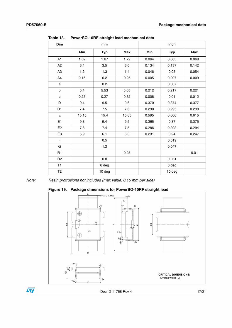
Note: Resin protrusions not included (max value: 0.15 mm per side)
Figure 19. Package dimensions for PowerSO-10RF straight lead
Table 13. PowerSO-10RF straight lead mechanical data
Dim mm Inch
Min Typ Max Min Typ Max
A1 1.62 1.67 1.72 0.064 0.065 0.068
A2 3.4 3.5 3.6 0.134 0.137 0.142
A3 1.2 1.3 1.4 0.046 0.05 0.054
A4 0.15 0.2 0.25 0.005 0.007 0.009
a 0.2 0.007
b 5.4 5.53 5.65 0.212 0.217 0.221
c 0.23 0.27 0.32 0.008 0.01 0.012
D 9.4 9.5 9.6 0.370 0.374 0.377
D1 7.4 7.5 7.6 0.290 0.295 0.298
E 15.15 15.4 15.65 0.595 0.606 0.615
E1 9.3 9.4 9.5 0.365 0.37 0.375
E2 7.3 7.4 7.5 0.286 0.292 0.294
E3 5.9 6.1 6.3 0.231 0.24 0.247
F 0.5 0.019
G 1.2 0.047
R1 0.25 0.01
R2 0.8 0.031
T1 6 deg 6 deg
T2 10 deg 10 deg
CRITICAL DIMENSIONS:- Overall width (L)
Package mechanical data PD57060-E
18/21 Doc ID 11758 Rev 4
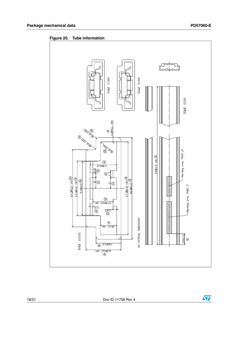
Figure 20. Tube information

PD57060-E Package mechanical data
Doc ID 11758 Rev 4 19/21
Figure 21. Reel information
Revision history PD57060-E
20/21 Doc ID 11758 Rev 4
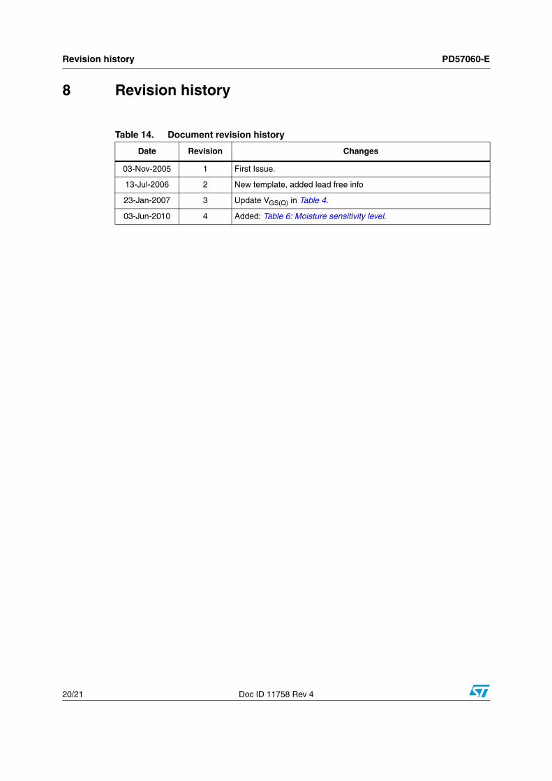
8 Revision history
Table 14. Document revision history
Date Revision Changes
03-Nov-2005 1 First Issue.
13-Jul-2006 2 New template, added lead free info
23-Jan-2007 3 Update VGS(Q) in Table 4.
03-Jun-2010 4 Added: Table 6: Moisture sensitivity level.

PD57060-E
Doc ID 11758 Rev 4 21/21
Please Read Carefully:
Information in this document is provided solely in connection with ST products. STMicroelectronics NV and its subsidiaries (“ST”) reserve theright to make changes, corrections, modifications or improvements, to this document, and the products and services described herein at anytime, without notice.
All ST products are sold pursuant to ST’s terms and conditions of sale.
Purchasers are solely responsible for the choice, selection and use of the ST products and services described herein, and ST assumes noliability whatsoever relating to the choice, selection or use of the ST products and services described herein.
No license, express or implied, by estoppel or otherwise, to any intellectual property rights is granted under this document. If any part of thisdocument refers to any third party products or services it shall not be deemed a license grant by ST for the use of such third party productsor services, or any intellectual property contained therein or considered as a warranty covering the use in any manner whatsoever of suchthird party products or services or any intellectual property contained therein.
UNLESS OTHERWISE SET FORTH IN ST’S TERMS AND CONDITIONS OF SALE ST DISCLAIMS ANY EXPRESS OR IMPLIEDWARRANTY WITH RESPECT TO THE USE AND/OR SALE OF ST PRODUCTS INCLUDING WITHOUT LIMITATION IMPLIEDWARRANTIES OF MERCHANTABILITY, FITNESS FOR A PARTICULAR PURPOSE (AND THEIR EQUIVALENTS UNDER THE LAWSOF ANY JURISDICTION), OR INFRINGEMENT OF ANY PATENT, COPYRIGHT OR OTHER INTELLECTUAL PROPERTY RIGHT.
UNLESS EXPRESSLY APPROVED IN WRITING BY AN AUTHORIZED ST REPRESENTATIVE, ST PRODUCTS ARE NOTRECOMMENDED, AUTHORIZED OR WARRANTED FOR USE IN MILITARY, AIR CRAFT, SPACE, LIFE SAVING, OR LIFE SUSTAININGAPPLICATIONS, NOR IN PRODUCTS OR SYSTEMS WHERE FAILURE OR MALFUNCTION MAY RESULT IN PERSONAL INJURY,DEATH, OR SEVERE PROPERTY OR ENVIRONMENTAL DAMAGE. ST PRODUCTS WHICH ARE NOT SPECIFIED AS "AUTOMOTIVEGRADE" MAY ONLY BE USED IN AUTOMOTIVE APPLICATIONS AT USER’S OWN RISK.
Resale of ST products with provisions different from the statements and/or technical features set forth in this document shall immediately voidany warranty granted by ST for the ST product or service described herein and shall not create or extend in any manner whatsoever, anyliability of ST.
ST and the ST logo are trademarks or registered trademarks of ST in various countries.
Information in this document supersedes and replaces all information previously supplied.
The ST logo is a registered trademark of STMicroelectronics. All other names are the property of their respective owners.
© 2010 STMicroelectronics - All rights reserved
STMicroelectronics group of companies
Australia - Belgium - Brazil - Canada - China - Czech Republic - Finland - France - Germany - Hong Kong - India - Israel - Italy - Japan - Malaysia - Malta - Morocco - Philippines - Singapore - Spain - Sweden - Switzerland - United Kingdom - United States of America
www.st.com