rethinking the hierarchy of electronic interconnections
TRANSCRIPT
Rethinking the Hierarchy ofElectronic Interconnections
Joseph FjelstadVerdant Electronics

The Industry’s Terminology Challenge
» The electronics industry continues to explore and develop new methods to fabricate and interconnect its electrical and electronic devices.
» Establishing an understanding of how various elements fit together hierarchically is vital to extracting full benefit of technological progress in interconnection design architecture
» Trying to keep pace in classifying and incorporating the various approaches to new interconnection schemes is proving quite challenging (e.g. new 2.5 and 3D solutions)
» The commonly accepted approach to illustrating how the elements of the electronic interconnection fit is rooted in a hierarchy that was developed in the 1960 & 70s
» Unfortunately it no longer works for today’s more complex approaches to the interconnection of electronic elements

Product/System/BoxAssembly
Traditional Hierarchy of Interconnections
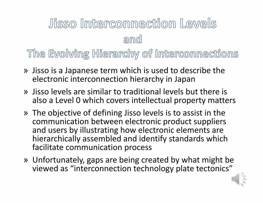
» Jisso is a Japanese term which is used to describe the electronic interconnection hierarchy in Japan
» Jisso levels are similar to traditional levels but there is also a Level 0 which covers intellectual property matters
» The objective of defining Jisso levels is to assist in the communication between electronic product suppliers and users by illustrating how electronic elements are hierarchically assembled and identify standards which facilitate communication process
» Unfortunately, gaps are being created by what might be viewed as “interconnection technology plate tectonics”
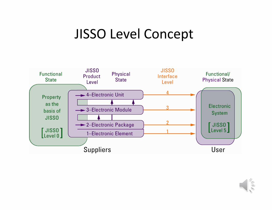
JISSO Level Concept

JISSO Level Concept…
Alternate view

Stacked Wafer with TSV Wafer Level
PackagesStacked Chip/
Multichip Packages(e.g, System in Package)
Stacked Chip Packages
(e.g.,PoP, PiP, PuP)
Stacked Embedded DeviceStructures
Product/System/BoxAssembly
(e.g., Occam/SolderFree)
The Evolving Hierarchy of Interconnections
Embedded Device Assemblies

Evolving Technologies are Difficult to Neatly Categorize
• Many different solutions are being introduced• Wafer stacking, Chip Stacking, TSV • Multichip Packages
– System in Package (SiP)
– Package in Package (PiP)
– Package on Package (PoP)
– Package under Package (PuP)
Embedded device solutions
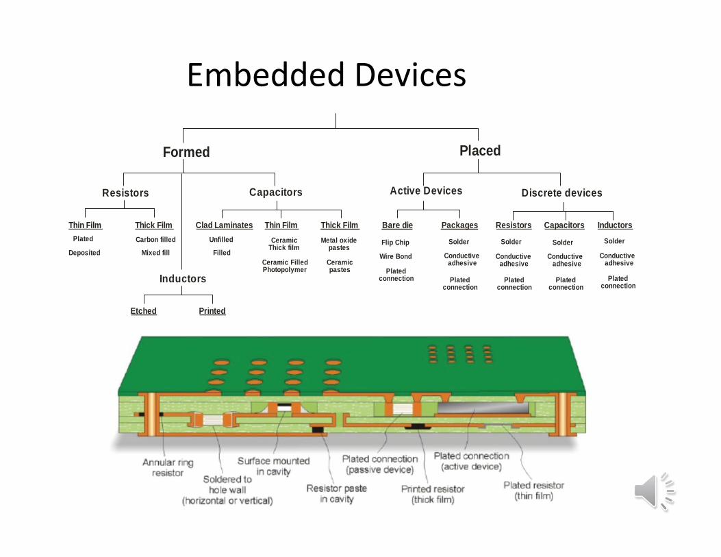
Formed Placed
Resistors
Inductors
Capacitors Active Devices Discrete devices
Thin Film
Etched
Thin FilmClad Laminates Packages Resistors Capacitors InductorsThick Film
Printed
Thick Film Bare diePlated Carbon filled
Mixed fillDeposited
Unfilled
FilledCeramic
Thick film
Ceramic Filled Photopolymer
Metal oxidepastes
Flip Chip Solder Solder SolderSolder
Conductive adhesive
Conductive adhesive
Conductive adhesive
Conductive adhesive
Wire Bond
Plated connection Plated
connectionPlated
connectionPlated
connectionPlated
connection
Ceramicpastes
Embedded Devices

Evolving Technologies are Difficult to Neatly Categorize
» Many different solutions are being introduced» Wafer stacking, Chip Stacking, TSV » Multichip Packages
– System in Package (SiP)
– Package in Package (PiP)
– Package on Package (PoP)
– Package under Package (PuP)
Embedded device solutions Solder Alloy Free Electronics (SAFE)

Solderless Assembly for Electronics (SAFE)

Flexible circuits
Metal core embedded device assemblies
Thermal spreader/Mezzanine connector
Assembly

Terminology Gap ChallengeUnfortunately current Jisso and traditional levels do not clearly define the various interconnection technology gaps and the differences they entail…
The question for the industry is: How might JIC and the electronics industry respond this ongoing challenge and capture the changes?

Possible Solution 1Increase the number of Jisso levels?
˃ Level 1 On chip interconnections (includes discrete devices)
˃ Level 2 Off chip interconnections (either side)
˃ Level 3 Chip to chip interconnections (any method)
˃ Level 4 Chip to package interconnections (any direction)
˃ Level 5 Package to package interconnections (any direction)
˃ Level 6 Embedded device structures (with or without solder)
˃ Level 7 Package to substrate interconnection (with solder)
˃ Level 8 Substrate to substrate interconnection (any direction)
˃ Level 9 System interconnections

Possible Solution 2Create intermediate Jisso levels?
˃ Level 1 On chip interconnections (includes discrete devices)
˃ Level 1a Off chip interconnections (either side)
˃ Level 1b Chip to chip interconnections (any method)
˃ Level 1c Chip to package interconnections (any direction)
˃ Level 2a Package to package interconnections (any direction)
˃ Level 2b Embedded device structures (with or without solder)
˃ Level 3a Package to substrate interconnection (with solder)
˃ Level 3b Package to substrate interconnection (socket, connector)
˃ Level 4 Substrate to substrate interconnection (edge card, 2 piece)
˃ Level 5 System interconnections (cables, connectors)

Summary» The realm of electronic interconnections is evolving at a
rapid clip and has already moved and is still moving in some unpredictable ways.
» To assure reliable communication between package and system designers, developers and fabricators while simultaneously allowing them to access the latest technologies, there will be need to understand, adapt to and embrace the rapid pace of change occurring in the electronics packaging and interconnection industry.
» These new solutions offer great promise but do also require a good amount of understanding and discipline to implement and harness their benefit
» Good communications will be key to the success of all

For More Information Visit
http://jisso.ipc.org/