reference guide - texas instruments page 0 / register 3: reserved register -0x00 / 0x03..... 80...
TRANSCRIPT
TLV320DAC3203 Applications
Reference Guide
Literature Number: SLAU434
May 2012

Contents
1 TLV320DAC3203 Overview ................................................................................................. 101.1 Description ................................................................................................................. 101.2 Typical Circuit Configuration ............................................................................................. 11
2 TLV320DAC3203 Application .............................................................................................. 122.1 Terminal Descriptions ..................................................................................................... 12
2.1.1 Digital Pins ........................................................................................................ 122.1.2 Analog Pins ........................................................................................................ 122.1.3 Multifunction Pins ................................................................................................. 122.1.4 Register Settings for Multifunction Pins ....................................................................... 14
2.2 Analog Audio I/O .......................................................................................................... 152.2.1 Analog Low Power Bypass ...................................................................................... 152.2.2 Headphone Output ............................................................................................... 16
2.3 Digital Microphone Input/Decimation Filter ............................................................................. 212.3.1 Digital Microphone Interface .................................................................................... 212.3.2 Digital Volume Control ........................................................................................... 222.3.3 Digital Microphone Decimation Filtering and Signal Processing Overview ............................... 22
2.4 DAC ......................................................................................................................... 352.4.1 Processing Blocks – Details ..................................................................................... 362.4.2 User Programmable Filters ...................................................................................... 392.4.3 Interpolation Filters ............................................................................................... 422.4.4 DAC Gain Setting ................................................................................................. 442.4.5 DAC Special Functions .......................................................................................... 472.4.6 DAC Setup ........................................................................................................ 48
2.5 PowerTune ................................................................................................................. 492.5.1 PowerTune Modes ............................................................................................... 492.5.2 DAC Power Consumption ....................................................................................... 51
2.6 Audio Digital I/O Interface ................................................................................................ 562.6.1 Right Justified Mode ............................................................................................. 572.6.2 Left Justified Mode ............................................................................................... 582.6.3 I2S Mode ........................................................................................................... 592.6.4 DSP Mode ......................................................................................................... 602.6.5 Secondary I2S ..................................................................................................... 61
2.7 Clock Generation and PLL ............................................................................................... 622.7.1 PLL ................................................................................................................. 65
2.8 Control Interfaces .......................................................................................................... 662.8.1 I2C Control Mode ................................................................................................. 662.8.2 SPI Digital Interface .............................................................................................. 68
2.9 Power Supply .............................................................................................................. 692.9.1 System Level Considerations ................................................................................... 69
2.10 Reference Voltage ......................................................................................................... 702.11 Device Special Functions ................................................................................................. 71
2.11.1 Interrupts ......................................................................................................... 71
3 Device Initialization ............................................................................................................ 723.1 Reset ........................................................................................................................ 733.2 Device Startup Lockout Times ........................................................................................... 73
2 Contents SLAU434–May 2012Submit Documentation Feedback
Copyright © 2012, Texas Instruments Incorporated
www.ti.com
3.3 Analog and Reference Startup .......................................................................................... 733.4 PLL Startup ................................................................................................................. 733.5 Setting Device Common Mode Voltage ................................................................................ 73
4 Example Setups ................................................................................................................ 744.1 Stereo DAC Playback with 48ksps Sample Rate and High Performance. ......................................... 744.2 Stereo DAC Playback with 48ksps Sample Rate and Low Power Mode .......................................... 754.3 DAC Playback with 48ksps Sample Rate through Class-D Headphone Amplifiers .............................. 754.4 ADC Record through Digital Microphone with 44.1ksps Sample Rate ............................................. 774.5 Register Script for Mono DAC playback with 48ksps on Differential Headphone with Offset Calibration ..... 77
5 Register Map ..................................................................................................................... 795.1 Register Map Summary ................................................................................................... 795.2 Page 0 Registers .......................................................................................................... 79
5.2.1 Page 0 / Register 0: Page Select Register - 0x00 / 0x00 ............................................... 795.2.2 Page 0 / Register 1: Software Reset Register - 0x00 / 0x01 ............................................ 795.2.3 Page 0 / Register 2: Reserved Register - 0x00 / 0x02 .................................................. 795.2.4 Page 0 / Register 3: Reserved Register - 0x00 / 0x03 .................................................. 805.2.5 Page 0 / Register 4: Clock Setting Register 1, Multiplexers - 0x00 / 0x04 ............................ 805.2.6 Page 0 / Register 5: Clock Setting Register 2, PLL P&R Values - 0x00 / 0x05 ...................... 805.2.7 Page 0 / Register 6: Clock Setting Register 3, PLL J Values - 0x00 / 0x06 .......................... 805.2.8 Page 0 / Register 7: Clock Setting Register 4, PLL D Values (MSB) - 0x00 / 0x07 ................. 805.2.9 Page 0 / Register 8: Clock Setting Register 5, PLL D Values (LSB) - 0x00 / 0x08 .................. 815.2.10 Page 0 / Register 9-10: Reserved Register - 0x00 / 0x09-0x0A ........................................ 815.2.11 Page 0 / Register 11: Clock Setting Register 6, NDAC Values - 0x00 / 0x0B ........................ 815.2.12 Page 0 / Register 12: Clock Setting Register 7, MDAC Values - 0x00 / 0x0C ....................... 815.2.13 Page 0 / Register 13: DAC OSR Setting Register 1, MSB Value - 0x00 / 0x0D ..................... 825.2.14 Page 0 / Register 14: DAC OSR Setting Register 2, LSB Value - 0x00 / 0x0E ...................... 825.2.15 Page 0 / Register 15: Reserved Register - 0x00 / 0x0F ................................................. 825.2.16 Page 0 / Register 16: Reserved Register - 0x00 / 0x10 ................................................. 825.2.17 Page 0 / Register 17: Reserved Register - 0x00 / 0x11 ................................................. 825.2.18 Page 0 / Register 18: Reserved Register - 0x00 / 0x12 ................................................. 825.2.19 Page 0 / Register 19: Reserved Register - 0x00 / 0x13 ................................................. 825.2.20 Page 0 / Register 20: ADC Oversampling (AOSR) Register - 0x00 / 0x14 ........................... 835.2.21 Page 0 / Register 21: Reserved Register - 0x00 / 0x15 ................................................. 835.2.22 Page 0 / Register 22: Reserved Register - 0x00 / 0x16 ................................................. 835.2.23 Page 0 / Register 23: Reserved Register - 0x00 / 0x17 ................................................. 835.2.24 Page 0 / Register 24: Reserved Register - 0x00 / 0x18 ................................................. 835.2.25 Page 0 / Register 25: Clock Setting Register 8, Multiplexers - 0x00 / 0x19 .......................... 835.2.26 Page 0 / Register 26: Clock Setting Register 9, CLKOUT M divider value - 0x00 / 0x1A .......... 835.2.27 Page 0 / Register 27: Audio Interface Setting Register 1 - 0x00 / 0x1B ............................... 845.2.28 Page 0 / Register 28: Audio Interface Setting Register 2, Data offset setting - 0x00 / 0x1C ....... 845.2.29 Page 0 / Register 29: Audio Interface Setting Register 3 - 0x00 / 0x1D .............................. 845.2.30 Page 0 / Register 30: Clock Setting Register 10, BCLK N Divider - 0x00 / 0x1E .................... 845.2.31 Page 0 / Register 31: Audio Interface Setting Register 4, Secondary Audio Interface - 0x00 / 0x1F
................................................................................................................... 855.2.32 Page 0 / Register 32: Audio Interface Setting Register 5 - 0x00 / 0x20 ............................... 855.2.33 Page 0 / Register 33: Audio Interface Setting Register 6 - 0x00 / 0x21 ............................... 855.2.34 Page 0 / Register 34: Digital Interface Misc. Setting Register - 0x00 / 0x22 ......................... 865.2.35 Page 0 / Register 35-36: Reserved Register - 0x00 / 0x23-0x24 ...................................... 865.2.36 Page 0 / Register 37: DAC Flag Register 1 - 0x00 / 0x25 .............................................. 865.2.37 Page 0 / Register 38: DAC Flag Register 2 - 0x00 / 0x26 .............................................. 865.2.38 Page 0 / Register 39-41: Reserved Register - 0x00 / 0x27-0x29 ...................................... 875.2.39 Page 0 / Register 42: Sticky Flag Register 1 - 0x00 / 0x2A ............................................. 875.2.40 Page 0 / Register 43: Interrupt Flag Register 1 - 0x00 / 0x2B .......................................... 87
3SLAU434–May 2012 ContentsSubmit Documentation Feedback
Copyright © 2012, Texas Instruments Incorporated

www.ti.com
5.2.41 Page 0 / Register 44: Sticky Flag Register 2 - 0x00 / 0x2C ............................................. 875.2.42 Page 0 / Register 45: Reserved Register - 0x00 / 0x2D ................................................. 885.2.43 Page 0 / Register 46: Interrupt Flag Register 2 - 0x00 / 0x2E .......................................... 885.2.44 Page 0 / Register 47: Reserved Register - 0x00 / 0x2F ................................................. 885.2.45 Page 0 / Register 48: INT1 Interrupt Control Register - 0x00 / 0x30 .................................. 885.2.46 Page 0 / Register 49: INT2 Interrupt Control Register - 0x00 / 0x31 .................................. 895.2.47 Page 0 / Register 50-51: Reserved Register - 0x00 / 0x32-0x33 ...................................... 895.2.48 Page 0 / Register 52: GPIO/MFP5 Control Register (** Availble only for WCSP Package) - 0x00 /
0x34 ............................................................................................................. 895.2.49 Page 0 / Register 53: MFP2 Function Control Register - 0x00 / 0x35 ................................. 905.2.50 Page 0 / Register 54: DIN/MFP1 Function Control Register - 0x00 / 0x36 ........................... 905.2.51 Page 0 / Register 55: MISO/MFP4 Function Control Register - 0x00 / 0x37 ......................... 905.2.52 Page 0 / Register 56: SCLK/MFP3 Function Control Register - 0x00 / 0x38 ......................... 915.2.53 Page 0 / Register 57-59: Reserved Registers - 0x00 / 0x39-0x3B ..................................... 915.2.54 Page 0 / Register 60: DAC Signal Processing Block Control Register - 0x00 / 0x3C ............... 915.2.55 Page 0 / Register 61: Reserved Register - 0x00 / 0x3D ................................................. 915.2.56 Page 0 / Register 62: Reserved Register - 0x00 / 0x3E ................................................. 925.2.57 Page 0 / Register 63: DAC Channel Setup Register 1 - 0x00 / 0x3F .................................. 925.2.58 Page 0 / Register 64: DAC Channel Setup Register 2 - 0x00 / 0x40 .................................. 925.2.59 Page 0 / Register 65: Left DAC Channel Digital Volume Control Register - 0x00 / 0x41 ........... 935.2.60 Page 0 / Register 66: Right DAC Channel Digital Volume Control Register - 0x00 / 0x42 ......... 935.2.61 Page 0 / Register 67: Headset Detection Configuration Register - 0x00 / 0x43 ..................... 935.2.62 Page 0 / Register 68: DRC Control Register 1 - 0x00 / 0x44 ........................................... 945.2.63 Page 0 / Register 69: DRC Control Register 2 - 0x00 / 0x45 ........................................... 945.2.64 Page 0 / Register 70: DRC Control Register 3 - 0x00 / 0x46 ........................................... 945.2.65 Page 0 / Register 71: Beep Generator Register 1 - 0x00 / 0x47 ....................................... 955.2.66 Page 0 / Register 72: Beep Generator Register 2 - 0x00 / 0x48 ....................................... 955.2.67 Page 0 / Register 73: Beep Generator Register 3 - 0x00 / 0x49 ....................................... 955.2.68 Page 0 / Register 74: Beep Generator Register 4 - 0x00 / 0x4A ....................................... 955.2.69 Page 0 / Register 75: Beep Generator Register 5 - 0x00 / 0x4B ....................................... 955.2.70 Page 0 / Register 76: Beep Generator Register 6 - 0x00 / 0x4C ....................................... 965.2.71 Page 0 / Register 77: Beep Generator Register 7 - 0x00 / 0x4D ....................................... 965.2.72 Page 0 / Register 78: Beep Generator Register 8 - 0x00 / 0x4E ....................................... 965.2.73 Page 0 / Register 79: Beep Generator Register 9 - 0x00 / 0x4F ....................................... 965.2.74 Page 0 / Register 80: Reserved Register - 0x00 / 0x50 ................................................. 965.2.75 Page 0 / Register 82: Reserved Register - 0x00 / 0x52 ................................................. 975.2.76 Page 0 / Register 83: Left ADC Channel Volume Control Register - 0x00 / 0x53 ................... 975.2.77 Page 0 / Register 84: Right ADC Channel Volume Control Register - 0x00 / 0x54 ................. 975.2.78 Page 0 / Register 85: ADC Phase Adjust Register - 0x00 / 0x55 ...................................... 985.2.79 Page 0 / Register 80-127: Reserved Register - 0x00 / 0x50-0x7F ..................................... 98
5.3 Page 1 Registers .......................................................................................................... 985.3.1 Page 1 / Register 0: Page Select Register - 0x01 / 0x00 ............................................... 985.3.2 Page 1 / Register 1: Power Configuration Register - 0x01 / 0x01 ...................................... 985.3.3 Page 1 / Register 2: LDO Control Register - 0x01 / 0x02 ............................................... 985.3.4 Page 1 / Register 3: Playback Configuration Register 1 - 0x01 / 0x03 ................................ 995.3.5 Page 1 / Register 4: Playback Configuration Register 2 - 0x01 / 0x04 ................................ 995.3.6 Page 1 / Register 5-8: Reserved Register - 0x01 / 0x05-0x08 ......................................... 995.3.7 Page 1 / Register 9: Output Driver Power Control Register - 0x01 / 0x09 ............................ 995.3.8 Page 1 / Register 10: Common Mode Control Register - 0x01 / 0x0A ................................ 995.3.9 Page 1 / Register 11: Over Current Protection Configuration Register - 0x01 / 0x0B ............. 1005.3.10 Page 1 / Register 12: HPL Routing Selection Register - 0x01 / 0x0C ............................... 1005.3.11 Page 1 / Register 13: HPR Routing Selection Register - 0x01 / 0x0D ............................... 1005.3.12 Page 1 / Register 14-15: Reserved Register - 0x01 / 0x0E-0x0F .................................... 1005.3.13 Page 1 / Register 16: HPL Driver Gain Setting Register - 0x01 / 0x10 .............................. 100
4 Contents SLAU434–May 2012Submit Documentation Feedback
Copyright © 2012, Texas Instruments Incorporated

www.ti.com
5.3.14 Page 1 / Register 17: HPR Driver Gain Setting Register - 0x01 / 0x11 .............................. 1015.3.15 Page 1 / Register 18-19: Reserved Register - 0x01 / 0x12-0x13 ..................................... 1015.3.16 Page 1 / Register 20: Headphone Driver Startup Control Register - 0x01 / 0x14 .................. 1015.3.17 Page 1 / Register 21: Reserved Register - 0x01 / 0x15 ............................................... 1025.3.18 Page 1 / Register 22: INL to HPL Volume Control Register - 0x01 / 0x16 .......................... 1025.3.19 Page 1 / Register 23: INR to HPR Volume Control Register - 0x01 / 0x17 ......................... 1045.3.20 Page 1 / Register 24-50: Reserved Register - 0x01 / 0x18-0x32 ..................................... 1065.3.21 Page 1 / Register 51: MICBIAS Configuration Register - 0x01 / 0x33 ............................... 1065.3.22 Page 1 / Register 52-57: Reserved Register - 0x01 / 0x34-0x39 ..................................... 1075.3.23 Page 1 / Register 58: Analog Input Settings - 0x01 / 0x3A ............................................ 1075.3.24 Page 1 / Register 59-62: Reserved Register - 0x01 / 0x3B-0x3E .................................... 1075.3.25 Page 1 / Register 63: DAC Analog Gain Control Flag Register - 0x01 / 0x3F ...................... 1075.3.26 Page 1 / Register 64-70: Reserved Register - 0x01 / 0x40-0x46 ..................................... 1075.3.27 Page 1 / Register 71: Analog Input Quick Charging Configuration Register - 0x01 / 0x47 ........ 1085.3.28 Page 1 / Register 72-122: Reserved Register - 0x01 / 0x48-0x7A ................................... 1085.3.29 Page 1 / Register 123: Reference Power-up Configuration Register - 0x01 / 0x7B ................ 1085.3.30 Page 1 / Register 124: Reserved Register - 0x01 / 0x7C .............................................. 1085.3.31 Page 1 / Register 125: Offset Callibration Register - 0x01 / 0x7D .................................... 1085.3.32 Page 1 / Register 126-127: Reserved Register - 0x01 / 0x7E-0x7F ................................. 108
5.4 Page 8 Registers ......................................................................................................... 1095.4.1 Page 8 / Register 0: Page Select Register - 0x08 / 0x00 .............................................. 1095.4.2 Page 8 / Register 1: ADC Adaptive Filter Configuration Register - 0x08 / 0x01 .................... 1095.4.3 Page 8 / Register 2-7: Reserved - 0x08 / 0x02-0x07 ................................................... 1095.4.4 Page 8 / Register 8-127: ADC Coefficients Buffer-A C(0:29) - 0x08 / 0x08-0x7F .................. 109
5.5 Page 9 Registers ......................................................................................................... 1095.5.1 Page 9 / Register 0: Page Select Register - 0x09 / 0x00 .............................................. 1095.5.2 Page 9 / Register 1-7: Reserved - 0x09 / 0x01-0x07 ................................................... 1095.5.3 Page 9 / Register 8-15: ADC Coefficients Buffer-A C(30:31) - 0x09 / 0x08-0x0F .................. 1105.5.4 Page 9 / Register 16-31: Reserved - 0x09 / 0x10-0x1F ................................................ 1105.5.5 Page 9 / Register 32-127: ADC Coefficients Buffer-A C(36:59) - 0x09 / 0x20-0x7F ............... 110
5.6 Page 10 Registers ....................................................................................................... 1105.6.1 Page 10 / Register 0: Page Select Register - 0x0A / 0x00 ............................................ 1105.6.2 Page 10 / Register 1-7: Reserved - 0x0A / 0x01-0x07 ................................................. 1105.6.3 Page 10 / Register 8-23: ADC Coefficients Buffer-A C(60:63) - 0x0A / 0x08-0x17 ................ 1105.6.4 Page 10 / Register 24-127: Reserved - 0x0A / 0x18-0x7F ............................................ 110
5.7 Page 26 Registers ....................................................................................................... 1105.7.1 Page 26 / Register 0: Page Select Register - 0x1A / 0x00 ............................................ 1105.7.2 Page 26 / Register 1-7: Reserved. - 0x1A / 0x01-0x07 ................................................ 1115.7.3 Page 26 / Register 8-127: ADC Coefficients Buffer-B C(0:29) - 0x1A / 0x08-0x7F ................ 111
5.8 Page 27 Registers ....................................................................................................... 1115.8.1 Page 27 / Register 0: Page Select Register - 0x1B / 0x00 ............................................ 1115.8.2 Page 27 / Register 1-7: Reserved. - 0x1B / 0x01-0x07 ................................................ 1115.8.3 Page 27 / Register 8-15: ADC Coefficients Buffer-B C(30:31) - 0x1B / 0x08-0x0F ................ 1115.8.4 Page 27 / Register 16-31: Reserved. - 0x1B / 0x10-0x1F ............................................. 1115.8.5 Page 27 / Register 32-127: ADC Coefficients Buffer-B C(36:59) - 0x1B / 0x20-0x7F ............. 111
5.9 Page 28 Registers ....................................................................................................... 1115.9.1 Page 28 / Register 0: Page Select Register - 0x1C / 0x00 ............................................ 1115.9.2 Page 28 / Register 1-7: Reserved. - 0x1C / 0x01-0x07 ................................................ 1125.9.3 Page 28 / Register 8-23: ADC Coefficients Buffer-B C(60:63) - 0x1C / 0x08-0x17 ................ 1125.9.4 Page 28 / Register 24-127: Reserved. - 0x1C / 0x18-0x7F ........................................... 112
5.10 Page 44 Registers ....................................................................................................... 1125.10.1 Page 44 / Register 0: Page Select Register - 0x2C / 0x00 ............................................ 1125.10.2 Page 44 / Register 1: DAC Adaptive Filter Configuration Register - 0x2C / 0x01 .................. 112
5SLAU434–May 2012 ContentsSubmit Documentation Feedback
Copyright © 2012, Texas Instruments Incorporated
www.ti.com
5.10.3 Page 44 / Register 2-7: Reserved - 0x2C / 0x02-0x07 ................................................. 1125.10.4 Page 44 / Register 8-11: DAC Coefficients Buffer-A C(0:29) - 0x2C / 0x08-0x0B ................. 112
5.11 Page 45 Registers ....................................................................................................... 1135.11.1 Page 45 / Register 0: Page Select Register - 0x2D / 0x00 ............................................ 1135.11.2 Page 45 / Register 1-7: Reserved - 0x2D / 0x01-0x07 ................................................. 1135.11.3 Page 45 / Register 8-11: DAC Coefficients Buffer-A C(30) - 0x2D / 0x08-0x0B .................... 1135.11.4 Page 45 / Register 12-15: Reserved - 0x2D / 0x0C-0x0F ............................................. 1135.11.5 Page 45 / Register 16-127: DAC Coefficients Buffer-A C(32:59) - 0x2D / 0x10-0x7F ............. 113
5.12 Page 46 Registers ....................................................................................................... 1135.12.1 Page 46 / Register 0: Page Select Register - 0x2E / 0x00 ............................................ 1135.12.2 Page 46 / Register 1-7: Reserved - 0x2E / 0x01-0x07 ................................................. 1135.12.3 Page 46 / Register 8-19: DAC Coefficients Buffer-A C(60:62) - 0x2E / 0x08-0x13 ................ 1135.12.4 Page 46 / Register 20-27: Reserved - 0x2E / 0x14-0x1B .............................................. 1145.12.5 Page 46 / Register 28-75: DAC Coefficients Buffer-A C(65:76) - 0x2E / 0x1C-0x4B .............. 1145.12.6 Page 46 / Register 76-127: Reserved - 0x2E / 0x4C-0x7F ............................................ 114
5.13 Page 62 Registers ....................................................................................................... 1145.13.1 Page 62 / Register 0: Page Select Register - 0x3E / 0x00 ............................................ 1145.13.2 Page 62 / Register 1-7: Reserved. - 0x3E / 0x01-0x07 ................................................ 1145.13.3 Page 62 / Register 8-127: DAC Coefficients Buffer-B C(0:29) - 0x3E / 0x08-0x7F ................ 114
5.14 Page 63 Registers ....................................................................................................... 1145.14.1 Page 63 / Register 0: Page Select Register - 0x3F / 0x00 ............................................ 1145.14.2 Page 63 / Register 1-7: Reserved. - 0x3F / 0x01-0x07 ................................................ 1145.14.3 Page 63 / Register 8-11: DAC Coefficients Buffer-B C(30) - 0x3F / 0x08-0x0B .................... 1155.14.4 Page 63 / Register 12-15: Reserved. - 0x3F / 0x0C-0x0F ............................................. 1155.14.5 Page 63 / Register 16-127: DAC Coefficients Buffer-B C(32:59) - 0x3F / 0x10-0x7F ............. 115
5.15 Page 63 Registers ....................................................................................................... 1155.15.1 Page 63 / Register 0: Page Select Register - 0x3F / 0x00 ............................................ 1155.15.2 Page 63 / Register 1-7: Reserved - 0x3F / 0x01-0x07 ................................................. 1155.15.3 Page 63 / Register 8-19: DAC Coefficients Buffer-B C(60:62) - 0x3F / 0x08-0x13 ................ 1155.15.4 Page 63 / Register 20-27: Reserved - 0x3F / 0x14-0x1B .............................................. 1155.15.5 Page 63 / Register 28-75: DAC Coefficients Buffer-B C(65:76) - 0x3F / 0x1C-0x4B .............. 1155.15.6 Page 63 / Register 76-127: Reserved - 0x3F / 0x4C-0x7F ............................................ 116
5.16 ADC Coefficients A+B ................................................................................................... 1165.17 ADC Coefficient Default Values ........................................................................................ 1165.18 DAC Coefficients A+B ................................................................................................... 1175.19 DAC Coefficient Default Values ........................................................................................ 118
6 Contents SLAU434–May 2012Submit Documentation Feedback
Copyright © 2012, Texas Instruments Incorporated

www.ti.com
List of Figures
1-1. Simplified Block Diagram ................................................................................................. 10
1-2. Typical Circuit Configuration ............................................................................................. 11
2-1. Low Power Analog Bypass............................................................................................... 16
2-2. Stereo Headphone Configuration ....................................................................................... 16
2-3. Conceptual Circuit for Pop-Free Power-up ............................................................................ 17
2-4. Low Power Mono DAC to Differential Headphone .................................................................... 19
2-5. Configuration for Using Headphone Amplifier in Class-D Mode .................................................... 20
2-6. Digital Microphone in TLV320DAC3203 ............................................................................... 21
2-7. Timing Diagram for Digital Microphone Interface ..................................................................... 22
2-8. Signal Chain for PRB_R1 and PRB_R4................................................................................ 24
2-9. Signal Chain PRB_R2 and PRB_R5.................................................................................... 24
2-10. Signal Chain for PRB_R3 and PRB_R6................................................................................ 24
2-11. Signal Chain for PRB_R7 and PRB_R10 .............................................................................. 24
2-12. Signal Chain for PRB_R8 and PRB_R11 .............................................................................. 25
2-13. Signal Chain for PRB_R9 and PRB_R12 .............................................................................. 25
2-14. Signal Chain for PRB_R13 and PRB_R16............................................................................. 25
2-15. Signal Chain for PRB_R14 and PRB_R17............................................................................. 25
2-16. Signal for PRB_R15 and PRB_R18..................................................................................... 26
2-17. Decimation Filter A, Frequency Response ............................................................................ 30
2-18. Decimation Filter B, Frequency Response............................................................................. 31
2-19. Decimation Filter C, Frequency Response............................................................................. 32
2-20. Signal Chain for PRB_P1 and PRB_P4 ................................................................................ 36
2-21. Signal Chain for PRB_P2, PRB_P5, PRB_P10 and PRB_P15 ..................................................... 37
2-22. Signal Chain for PRB_P3, PRB_P6, PRB_P11 and PRB_P16 ..................................................... 37
2-23. Signal Chain for PRB_P7, PRB_P12, PRB_P17 and PRB_P20.................................................... 37
2-24. Signal Chain for PRB_P8 and PRB_P13............................................................................... 37
2-25. Signal Chain for PRB_P9 and PRB_P14............................................................................... 37
2-26. Signal Chain for PRB_P18 and PRB_P21 ............................................................................. 38
2-27. Signal Chain for PRB_P19 and PRB_P22 ............................................................................. 38
2-28. Signal Chain for PRB_P23 ............................................................................................... 38
2-29. Signal Chain for PRB_P24 ............................................................................................... 39
2-30. Signal Chain for PRB_P25 ............................................................................................... 39
2-31. DAC Interpolation Filter A, Frequency Response ..................................................................... 42
2-32. Channel Interpolation Filter B, Frequency Response................................................................. 43
2-33. DAC Interpolation Filter C, Frequency Response .................................................................... 43
2-34. Timing Diagram for Right-Justified Mode .............................................................................. 57
2-35. Timing Diagram for Left-Justified Mode ................................................................................ 58
2-36. Timing Diagram for Left-Justified Mode with Offset=1................................................................ 58
2-37. Timing Diagram for Left-Justified Mode with Offset=0 and inverted bit clock ..................................... 58
2-38. Timing Diagram for I2S Mode ............................................................................................ 59
2-39. Timing Diagram for I2S Mode with offset=2 ............................................................................ 59
2-40. Timing Diagram for I2S Mode with offset=0 and bit clock invert..................................................... 59
2-41. Timing Diagram for DSP Mode .......................................................................................... 60
2-42. Timing Diagram for DSP Mode with offset = 1 ........................................................................ 60
2-43. Timing Diagram for DSP Mode with offset = 0 and bit clock inverted .............................................. 60
2-44. Audio Serial Interface Multiplexing ...................................................................................... 61
2-45. Clock Distribution Tree.................................................................................................... 62
7SLAU434–May 2012 List of FiguresSubmit Documentation Feedback
Copyright © 2012, Texas Instruments Incorporated
www.ti.com
2-46. BCLK Output Options ..................................................................................................... 63
2-47. General Purpose Clock Output Options ................................................................................ 64
2-48. I2C Write .................................................................................................................... 67
2-49. I2C Read .................................................................................................................... 67
2-50. SPI Timing Diagram for Register Write................................................................................. 68
2-51. SPI Timing Diagram for Register Read................................................................................. 69
8 List of Figures SLAU434–May 2012Submit Documentation Feedback
Copyright © 2012, Texas Instruments Incorporated
www.ti.com
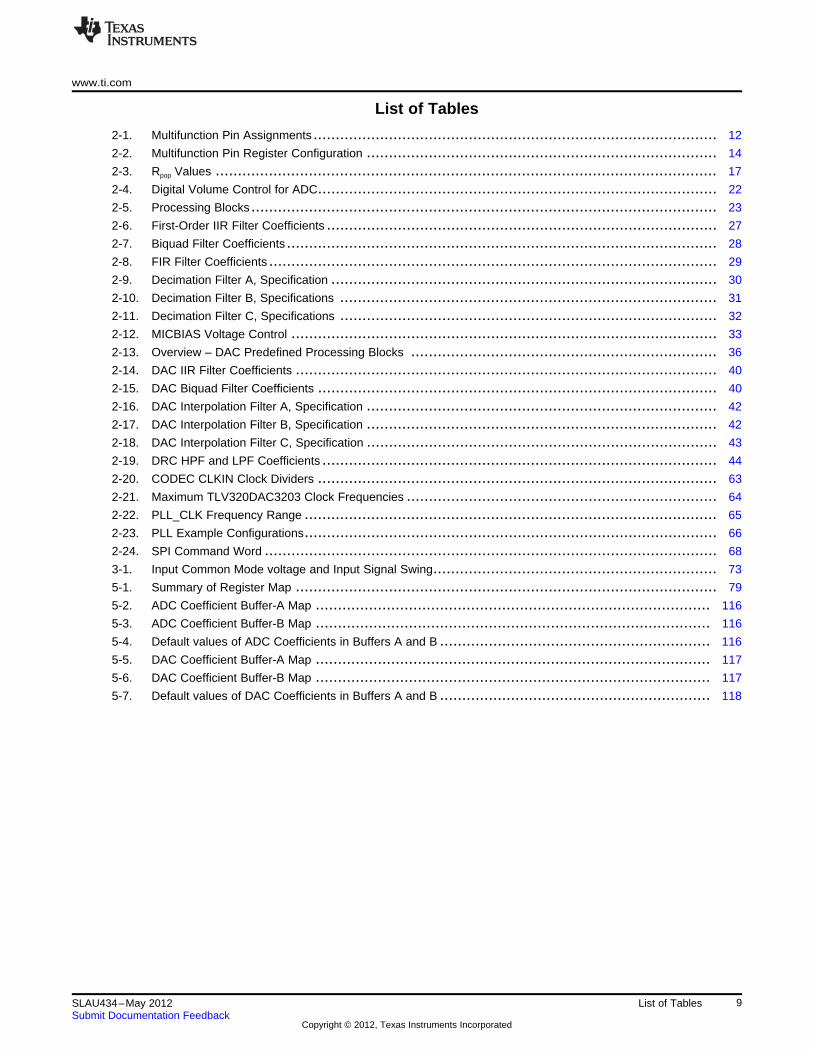
List of Tables
2-1. Multifunction Pin Assignments ........................................................................................... 12
2-2. Multifunction Pin Register Configuration ............................................................................... 14
2-3. Rpop Values ................................................................................................................. 17
2-4. Digital Volume Control for ADC.......................................................................................... 22
2-5. Processing Blocks ......................................................................................................... 23
2-6. First-Order IIR Filter Coefficients ........................................................................................ 27
2-7. Biquad Filter Coefficients ................................................................................................. 28
2-8. FIR Filter Coefficients ..................................................................................................... 29
2-9. Decimation Filter A, Specification ....................................................................................... 30
2-10. Decimation Filter B, Specifications ..................................................................................... 31
2-11. Decimation Filter C, Specifications ..................................................................................... 32
2-12. MICBIAS Voltage Control ................................................................................................ 33
2-13. Overview – DAC Predefined Processing Blocks ..................................................................... 36
2-14. DAC IIR Filter Coefficients ............................................................................................... 40
2-15. DAC Biquad Filter Coefficients .......................................................................................... 40
2-16. DAC Interpolation Filter A, Specification ............................................................................... 42
2-17. DAC Interpolation Filter B, Specification ............................................................................... 42
2-18. DAC Interpolation Filter C, Specification ............................................................................... 43
2-19. DRC HPF and LPF Coefficients ......................................................................................... 44
2-20. CODEC CLKIN Clock Dividers .......................................................................................... 63
2-21. Maximum TLV320DAC3203 Clock Frequencies ...................................................................... 64
2-22. PLL_CLK Frequency Range ............................................................................................. 65
2-23. PLL Example Configurations............................................................................................. 66
2-24. SPI Command Word ...................................................................................................... 68
3-1. Input Common Mode voltage and Input Signal Swing................................................................ 73
5-1. Summary of Register Map ............................................................................................... 79
5-2. ADC Coefficient Buffer-A Map ......................................................................................... 116
5-3. ADC Coefficient Buffer-B Map ......................................................................................... 116
5-4. Default values of ADC Coefficients in Buffers A and B ............................................................. 116
5-5. DAC Coefficient Buffer-A Map ......................................................................................... 117
5-6. DAC Coefficient Buffer-B Map ......................................................................................... 117
5-7. Default values of DAC Coefficients in Buffers A and B ............................................................. 118
9SLAU434–May 2012 List of TablesSubmit Documentation Feedback
Copyright © 2012, Texas Instruments Incorporated
Mic
bia
s
Sup
plie
s
SC
L/S
SZ
SD
A/M
OS
I
MC
LK
DO
UT
/MF
P2
DIN
/MF
P1
BC
LK
WC
LK
GP
IO
(WC
SP
On
ly)
Ref
Data
Inte
rfa
ce
Dig
Mic
Inte
rface
Chapter 1SLAU434–May 2012
TLV320DAC3203 Overview
1.1 Description
Features Applications
• Stereo Audio DAC with 100dB SNR • Headsets• 4.1mW Stereo 48ksps Playback • Handset Accessories• PowerTune™ • Communication• Extensive Signal Processing Options • Portable Computing• Stereo Digital Microphone Input –• Stereo Headphone Outputs • Chapter 1: Device Overview• Low Power Analog Bypass Mode • Chapter 2: TLV320DAC3203 Application• Programmable PLL • Chapter 3: Device Initialization• Integrated LDO • Chapter 4: Example Setups• 4mm × 4mm QFN and 2.7mm × 2.7mm • Chapter 5: Register Map and Descriptions
WCSPPackage
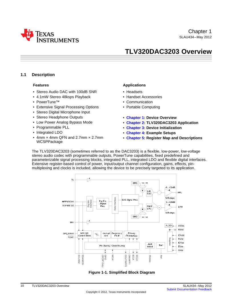
The TLV320DAC3203 (sometimes referred to as the DAC3203) is a flexible, low-power, low-voltagestereo audio codec with programmable outputs, PowerTune capabilities, fixed predefined andparameterizable signal processing blocks, integrated PLL, integrated LDO and flexible digital interfaces.Extensive register-based control of power, input/output channel configuration, gains, effects, pin-multiplexing and clocks is included, allowing the device to be precisely targeted to its application.
Figure 1-1. Simplified Block Diagram
10 TLV320DAC3203 Overview SLAU434–May 2012Submit Documentation Feedback
Copyright © 2012, Texas Instruments Incorporated

www.ti.com Typical Circuit Configuration
Combined with the advanced PowerTune technology, the device can cover operations from 8kHz monovoice playback to stereo 192kHz DAC playback, making it ideal for portable battery-powered audio andtelephony applications.
The record path of the TLV320DAC3203 consists of a stereo digital microphone PDM interface (notavailable when using SPI control interface) typically used at 64Fs or 128Fs.
The playback path offers signal processing blocks for filtering and effects, true differential output signal,flexible mixing of DAC and analog input signals as well as programmable volume controls. TheTLV320DAC3203 contains two high-power output drivers which can be configured in multiple ways,including stereo, and mono BTL. The integrated PowerTune technology allows the device to be tuned tojust the right power-performance trade-off. Mobile applications frequently have multiple use casesrequiring very low-power operation while being used in a mobile environment. When used in a dockedenvironment power consumption typically is less of a concern while lowest possible noise is important.With PowerTune the TLV320DAC3203 can address both cases.
The voltage supply range for the TLV320DAC3203 for analog is 1.5V–1.95V, and for digital it is1.26V–1.95V. To ease system-level design, a low-dropout regulator (LDO) is integrated to generate theappropriate analog supply from input voltages ranging from 1.8V to 3.6V. Digital I/O voltages aresupported in the range of 1.1V–3.6V.
The required internal clock of the TLV320DAC3203 can be derived from multiple sources, including theMCLK, BCLK or GPIO pins or the output of the internal PLL, where the input to the PLL again can bederived from the MCLK, BCLK or GPIO pins. Although using the internal, fractional PLL ensures theavailability of a suitable clock signal, it is not recommended for the lowest power settings. The PLL ishighly programmable and can accept available input clocks in the range of 512kHz to 50MHz.
The device is available in the 4mm × 4mm QFN and 2.7mm × 2.7mm WCSPpackage.
1.2 Typical Circuit Configuration
Figure 1-2. Typical Circuit Configuration
11SLAU434–May 2012 TLV320DAC3203 OverviewSubmit Documentation Feedback
Copyright © 2012, Texas Instruments Incorporated

Chapter 2SLAU434–May 2012
TLV320DAC3203 Application
2.1 Terminal Descriptions
2.1.1 Digital Pins
Only a small number of digital pins are dedicated to a single function; whenever possible, the digital pinshave a default function, and also can be reprogrammed to cover alternative functions for variousapplications.
The fixed-function pins are Reset and the SPI_Select pin, which are HW control pins. Depending on thestate of SPI_Select, the two control-bus pins SCL/SS and SDA/MOSI are configured for either I2C or SPIprotocol.
Other digital IO pins can be configured for various functions via register control. An overview of availablefunctionality is given in Section 2.1.3.
2.1.2 Analog Pins
Analog functions can also be configured to a large degree. For minimum power consumption, analogblocks are powered down by default. The blocks can be powered up with fine granularity according to theapplication needs.
2.1.3 Multifunction Pins
Table 2-1 shows the possible allocation of pins for specific functions. The PLL input, for example, can beprogrammed to be any of 4 pins (MCLK, BCLK, DIN, GPIO).
Table 2-1. Multifunction Pin Assignments
1 2 3 4 5 6 7 8
Pin Function MCLK BCLK WCLK DIN DOUT MFP3/ MFP4/ GPIOMFP1 MFP2 SCLK MISO MFP5
A PLL Input S (1) S (2) E S (3)
B Codec Clock Input S (1) ,D (4) S (2) S (3)
C I2S BCLK input S (2),D
D I2S BCLK output E (5)
E I2S WCLK input E, D
F I2S WCLK output E
G I2S ADC word clock input E E
H I2S ADC WCLK out E E
I I2S DIN E, D
J I2S DOUT E, D
K General Purpose Output I E
K General Purpose Output II E
(1) S(1): The MCLK pin can be used to drive the PLL and Codec Clock inputs simultaneously(2) S(2): The BCLK pin can be used to drive the PLL and Codec Clock and audio interface bit clock inputs simultaneously(3) S(3): The GPIO/MFP5 pin can be used to drive the PLL and Codec Clock inputs simultaneously(4) D: Default Function(5) E: The pin is exclusively used for this function, no other function can be implemented with the same pin (e.g. if GPIO/MFP5 has
been allocated for General Purpose Output, it cannot be used as the INT1 output at the same time)
12 TLV320DAC3203 Application SLAU434–May 2012Submit Documentation Feedback
Copyright © 2012, Texas Instruments Incorporated

www.ti.com Terminal Descriptions
Table 2-1. Multifunction Pin Assignments (continued)
1 2 3 4 5 6 7 8
Pin Function MCLK BCLK WCLK DIN DOUT MFP3/ MFP4/ GPIOMFP1 MFP2 SCLK MISO MFP5
K General Purpose Output III E
L General Purpose Input I E
L General Purpose Input II E
L General Purpose Input III E
M INT1 output E E E
N INT2 output E E E
Q Secondary I2S BCLK input E E
R Secondary I2S WCLK in E E
S Secondary I2S DIN E E
T Secondary I2S DOUT E
U Secondary I2S BCLK OUT E E E
V Secondary I2S WCLK OUT E E E
X Aux Clock Output E E E
13SLAU434–May 2012 TLV320DAC3203 ApplicationSubmit Documentation Feedback
Copyright © 2012, Texas Instruments Incorporated

Terminal Descriptions www.ti.com
2.1.4 Register Settings for Multifunction Pins
To configure the settings seen in Table 2-1, please see the letter/number combination in for theappropriate registers to modify. In , the letter/number combination represents the row and the columnnumber from Table 2-1 in bold type.
Please be aware that more settings may be necessary to obtain a full interface definition matching theapplication requirement (e.g. register Page 0 / Register 25 to 33).
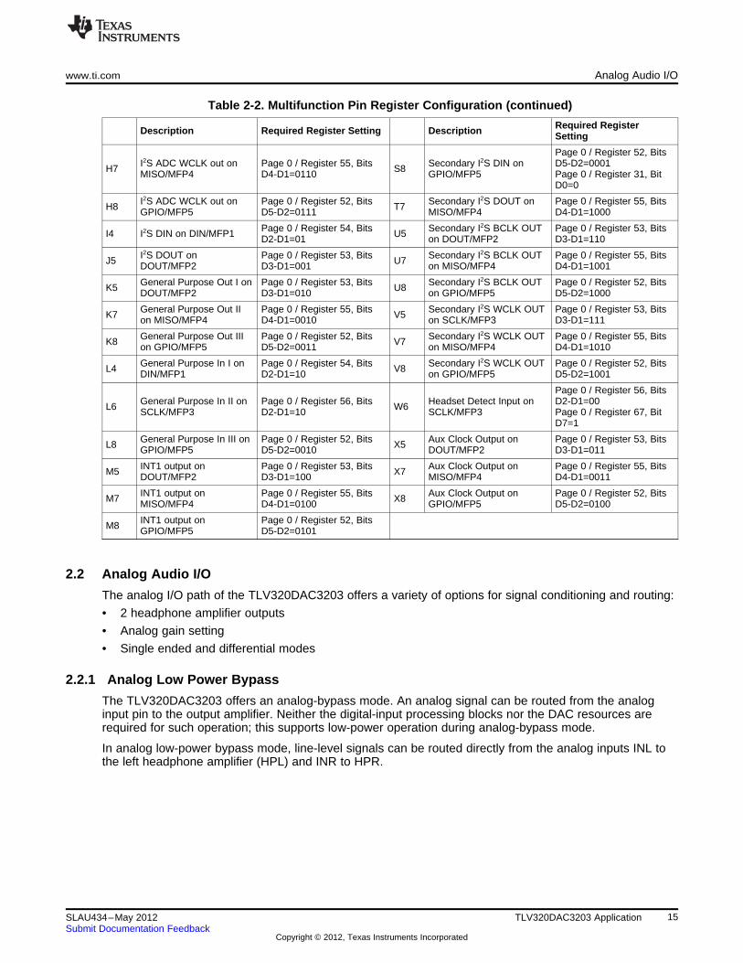
Table 2-2. Multifunction Pin Register Configuration
Required RegisterDescription Required Register Setting Description Setting
Page 0 / Register 4, Bits D3- Page 0 / Register 53,BitsA1 PLL Input on MCLK N5 INT2 output DOUT/MFP2D2=00 D3-D1=101
Page 0 / Register 4, Bits D3- INT2 output on Page 0 / Register 55, BitsA2 PLL Input on BCLK N7D2=01 MISO/MFP4 D4-D1=0101
Page 0 / Register 54, BitsD2-D1=01 INT2 output on Page 0 / Register 52, BitsA4 PLL Input on DIN/MFP1 N8Page 0 / Register 4, Bits D3- GPIO/MFP5 D5-D2=0110D2=11
Page 0 / Register 52, Bits Page 0 / Register 54, BitsD5-D2=0001 Digital Microphone Data D2-D1=01A8 PLL Input on GPIO/MFP5 O4Page 0 / Register 4, Bits D3- Input on DIN/MFP1 Page 0 / Register 81, BitsD2=10 D5-D4=10
Page 0 / Register 56, BitsCodec Clock Input on Page 0 / Register 4, Bits D1- Digital Microphone Data D2-D1=01B1 O6MCLK D0=00 Input on SCLK/MFP3 Page 0 / Register 81, Bits
D5-D4=01
Page 0 / Register 52, BitsCodec Clock Input on Page 0 / Register 4, Bits D1- Digital Microphone Data D5-D2=0001B2 O8BCLK D0=01 Input on GPIO/MFP5 Page 0 / Register 81, Bits
D5-D4=00
Page 0 / Register 52, BitsCodec Clock Input on D5-D2=0001 Digital Microphone Clock Page 0 / Register 55, BitsB8 P7GPIO/MPF5 Page 0 / Register 4, Bits D1- Output on MISO/MFP4 D4-D1=0111
D0=10
Page 0 / Register 27, Bit Digital Microphone Clock Page 0 / Register 52, BitsC2 I2S BCLK input on BCLK P8D3=0 Output on GPIO/MFP5 D5-D2=1010
Page 0 / Register 56, BitsPage 0 / Register 27, Bit Secondary I2S BCLK input D2-D1=01D2 I2S BCLK output on BCLK Q6D3=1 on SCLK/MFP3 Page 0 / Register 31, Bits
D6-D5=01
Page 0 / Register 52, BitsPage 0 / Register 27, Bit Secondary I2S BCLK input D5-D2=0001E3 I2S WCLK input on WCLK Q8D2=0 on GPIO/MFP5 Page 0 / Register 31, Bits
D6-D5=00
Page 0 / Register 56, BitsPage 0 / Register 27, Bit Secondary I2S WCLK in on D2-D1=01F3 I2S WCLK output WCLK R6D2=1 SCLK/MFP3 Page 0 / Register 31, Bits
D4-D3=01
Page 0 / Register 56, Bits Page 0 / Register 52, BitsI2S ADC word clock input D2-D1=01 Secondary I2S WCLK in on D5-D2=0001G6 R8on SCLK/MFP3 Page 0 / Register 31, Bits GPIO/MFP50 Page 0 / Register 31, Bits
D2-D1=01 D4-D3=0
Page 0 / Register 52, Bits Page 0 / Register 56, BitsI2S ADC word clock input D5-D2=0001 Secondary I2S DIN on D2-D1=01G8 S6on GPIO/MFP5 Page 0 / Register 31, Bits SCLK/MFP3 Page 0 / Register 31, Bit
D2-D1=00 D0=1
14 TLV320DAC3203 Application SLAU434–May 2012Submit Documentation Feedback
Copyright © 2012, Texas Instruments Incorporated
www.ti.com Analog Audio I/O
Table 2-2. Multifunction Pin Register Configuration (continued)
Required RegisterDescription Required Register Setting Description Setting
Page 0 / Register 52, BitsI2S ADC WCLK out on Page 0 / Register 55, Bits Secondary I2S DIN on D5-D2=0001H7 S8MISO/MFP4 D4-D1=0110 GPIO/MFP5 Page 0 / Register 31, Bit
D0=0
I2S ADC WCLK out on Page 0 / Register 52, Bits Secondary I2S DOUT on Page 0 / Register 55, BitsH8 T7GPIO/MFP5 D5-D2=0111 MISO/MFP4 D4-D1=1000
Page 0 / Register 54, Bits Secondary I2S BCLK OUT Page 0 / Register 53, BitsI4 I2S DIN on DIN/MFP1 U5D2-D1=01 on DOUT/MFP2 D3-D1=110
I2S DOUT on Page 0 / Register 53, Bits Secondary I2S BCLK OUT Page 0 / Register 55, BitsJ5 U7DOUT/MFP2 D3-D1=001 on MISO/MFP4 D4-D1=1001
General Purpose Out I on Page 0 / Register 53, Bits Secondary I2S BCLK OUT Page 0 / Register 52, BitsK5 U8DOUT/MFP2 D3-D1=010 on GPIO/MFP5 D5-D2=1000
General Purpose Out II Page 0 / Register 55, Bits Secondary I2S WCLK OUT Page 0 / Register 53, BitsK7 V5on MISO/MFP4 D4-D1=0010 on SCLK/MFP3 D3-D1=111
General Purpose Out III Page 0 / Register 52, Bits Secondary I2S WCLK OUT Page 0 / Register 55, BitsK8 V7on GPIO/MFP5 D5-D2=0011 on MISO/MFP4 D4-D1=1010
General Purpose In I on Page 0 / Register 54, Bits Secondary I2S WCLK OUT Page 0 / Register 52, BitsL4 V8DIN/MFP1 D2-D1=10 on GPIO/MFP5 D5-D2=1001
Page 0 / Register 56, BitsGeneral Purpose In II on Page 0 / Register 56, Bits Headset Detect Input on D2-D1=00L6 W6SCLK/MFP3 D2-D1=10 SCLK/MFP3 Page 0 / Register 67, Bit
D7=1
General Purpose In III on Page 0 / Register 52, Bits Aux Clock Output on Page 0 / Register 53, BitsL8 X5GPIO/MFP5 D5-D2=0010 DOUT/MFP2 D3-D1=011
INT1 output on Page 0 / Register 53, Bits Aux Clock Output on Page 0 / Register 55, BitsM5 X7DOUT/MFP2 D3-D1=100 MISO/MFP4 D4-D1=0011
INT1 output on Page 0 / Register 55, Bits Aux Clock Output on Page 0 / Register 52, BitsM7 X8MISO/MFP4 D4-D1=0100 GPIO/MFP5 D5-D2=0100
INT1 output on Page 0 / Register 52, BitsM8 GPIO/MFP5 D5-D2=0101
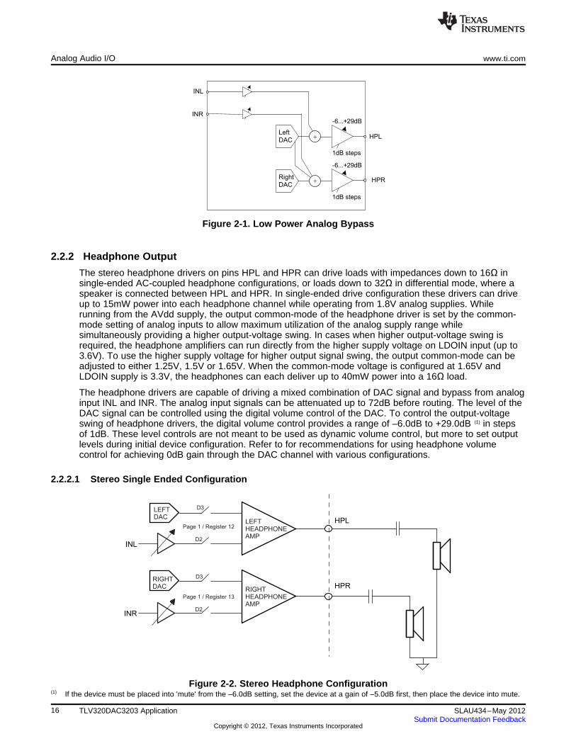
2.2 Analog Audio I/O
The analog I/O path of the TLV320DAC3203 offers a variety of options for signal conditioning and routing:
• 2 headphone amplifier outputs
• Analog gain setting
• Single ended and differential modes
2.2.1 Analog Low Power Bypass
The TLV320DAC3203 offers an analog-bypass mode. An analog signal can be routed from the analoginput pin to the output amplifier. Neither the digital-input processing blocks nor the DAC resources arerequired for such operation; this supports low-power operation during analog-bypass mode.
In analog low-power bypass mode, line-level signals can be routed directly from the analog inputs INL tothe left headphone amplifier (HPL) and INR to HPR.
15SLAU434–May 2012 TLV320DAC3203 ApplicationSubmit Documentation Feedback
Copyright © 2012, Texas Instruments Incorporated
HPL
HPR
LEFTDAC
RIGHTDAC
LEFTHEADPHONEAMP
RIGHTHEADPHONEAMP
INL
INR
Page 1 / Register 12
Page 1 / Register 13
D3
D2
D3
D2
Left
DAC+
+Right
DAC
-6...+29dB
1dB steps
-6...+29dB
1dB steps
HPL
HPR
INL
INR
Analog Audio I/O www.ti.com
Figure 2-1. Low Power Analog Bypass
2.2.2 Headphone Output
The stereo headphone drivers on pins HPL and HPR can drive loads with impedances down to 16Ω insingle-ended AC-coupled headphone configurations, or loads down to 32Ω in differential mode, where aspeaker is connected between HPL and HPR. In single-ended drive configuration these drivers can driveup to 15mW power into each headphone channel while operating from 1.8V analog supplies. Whilerunning from the AVdd supply, the output common-mode of the headphone driver is set by the common-mode setting of analog inputs to allow maximum utilization of the analog supply range whilesimultaneously providing a higher output-voltage swing. In cases when higher output-voltage swing isrequired, the headphone amplifiers can run directly from the higher supply voltage on LDOIN input (up to3.6V). To use the higher supply voltage for higher output signal swing, the output common-mode can beadjusted to either 1.25V, 1.5V or 1.65V. When the common-mode voltage is configured at 1.65V andLDOIN supply is 3.3V, the headphones can each deliver up to 40mW power into a 16Ω load.
The headphone drivers are capable of driving a mixed combination of DAC signal and bypass from analoginput INL and INR. The analog input signals can be attenuated up to 72dB before routing. The level of theDAC signal can be controlled using the digital volume control of the DAC. To control the output-voltageswing of headphone drivers, the digital volume control provides a range of –6.0dB to +29.0dB (1) in stepsof 1dB. These level controls are not meant to be used as dynamic volume control, but more to set outputlevels during initial device configuration. Refer to for recommendations for using headphone volumecontrol for achieving 0dB gain through the DAC channel with various configurations.
2.2.2.1 Stereo Single Ended Configuration
Figure 2-2. Stereo Headphone Configuration(1) If the device must be placed into 'mute' from the –6.0dB setting, set the device at a gain of –5.0dB first, then place the device into mute.
16 TLV320DAC3203 Application SLAU434–May 2012Submit Documentation Feedback
Copyright © 2012, Texas Instruments Incorporated

cmpopload
loadload V
RR
RV ´
+
=
Rload
Rpop
CcOutputDriver
PAD
www.ti.com Analog Audio I/O
The left and right DAC channels are routed to the corresponding left and right headphone amplifier. Thisconfiguration is also used to drive line-level loads.
The TLV320DAC3203 headphone drivers support pop-free operation. Because the HPL and HPR arehigh-power drivers, pop can result due to sudden transient changes in the output drivers if care is nottaken. The most critical care is required while using the drivers as stereo single-ended capacitively-coupled drivers as shown in Figure 2-2. The output drivers achieve pop-free power-up by using slowpower-up modes. Conceptually, the circuit during power-up can be visualized as
Figure 2-3. Conceptual Circuit for Pop-Free Power-up
The value of Rpop can be chosen by setting register Page 1, Register 20, Bits D1-D0).
Table 2-3. Rpop Values
Page 1, Register 20, Bits D1-D0) Rpop Value
00 2 kΩ01 6 kΩ10 25 kΩ
To minimize audible artifacts, two parameters can be adjusted to match application requirements. Thevoltage Vload across Rload at the beginning of slow charging should not be more than a few mV. At that timethe voltage across Rload can be determined as:
(1)
For a typical Rload of 32Ω, Rpop of 6 kΩ or 25 kΩ will deliver good results (see Table 2-3 for registersettings).
According to the conceptual circuit in Figure 2-3, the voltage on PAD will exponentially settle to the outputcommon-mode voltage based on the value of Rpop and Cc. Thus, the output drivers must be in slow power-up mode for time T, such that at the end of the slow power-on period, the voltage on Vpad is very close tothe common-mode voltage. The TLV320DAC3203 allows the time T to be adjusted to allow for a widerange of Rload and Cc by programming Page 1, Register 20, Bits D5-D2). For the time adjustments, thevalue of Cc is assumed to be 47μF. N=5 is expected to yield good results.
Page 1, Register 20, Bits D5- Slow Charging Time=N*Time – Constants(for Rpop and 47μF)D2)
0000 N=0
0001 N=0.5
0010 N=0.625
0011 N=0.75
0100 N=0.875
0101 N=1.0
0110 N=2.0
0111 N=3.0
1000 N=4.0
1001 N=5.0
17SLAU434–May 2012 TLV320DAC3203 ApplicationSubmit Documentation Feedback
Copyright © 2012, Texas Instruments Incorporated

Analog Audio I/O www.ti.com
Page 1, Register 20, Bits D5- Slow Charging Time=N*Time – Constants(for Rpop and 47μF)D2)
1010 N=6.0
1011 N=7.0
1100 N=8.0
1101 N=16 (Not valid for Rpop=25kΩ)
1110 N=24 (Not valid for Rpop=25kΩ)
1111 N=32 (Not valid for Rpop=25kΩ)
Again, for example, for Rload=32Ω, Cc=47μF and common mode of 0.9V, the number of time constantsrequired for pop-free operation is 5 or 6. A higher or lower Cc value will require higher or lower value for N.
During the slow-charging period, no signal is routed to the output driver. Therefore, choosing a larger thannecessary value of N results in a delay from power-up to signal at output. At the same time, choosing N tobe smaller than the optimal value results in poor pop performance at power-up.
The signals being routed to headphone drivers (e.g. DAC and IN) often have DC offsets due to less-than-ideal processing. As a result, when these signals are routed to output drivers, the offset voltage causes apop. To improve the pop-performance in such situations, a feature is provided to soft-step the DC-offset.At the beginning of the signal routing, a high-value attenuation can be applied which can be progressivelyreduced in steps until the desired gain in the channel is reached. The time interval between each of thesegain changes can be controlled by programming Page 1, Register 20, Bits D7-D6). This gain soft-steppingis applied only during the initial routing of the signal to the output driver and not during subsequent gainchanges.
Page 1, Register 20, Bits D7-D6 Soft-stepping Step Time During initial signal routing
00 0 ms (soft-stepping disabled)
01 50ms
10 100ms
11 200ms
It is recommended to use the following sequence for achieving optimal pop performance at power-up:
1. Choose the value of Rpop, N (time constants) and soft-stepping step time for slow power-up.
2. Choose the configuration for output drivers, including common modes and output stage powerconnections
3. Select the signals to be routed to headphones.
4. Power-up the blocks driving signals into HPL and HPR, but keep it muted
5. Unmute HPL and HPR and set the desired gain setting.
6. Power-on the HPL and HPR drivers.
7. Unmute the block driving signals to HPL and HPR after the Driver PGA flags are set to indicatecompletion of soft-stepping after power-up. These flags can be read from Page 1, Register 63, Bits D7-D6).
It is important to configure the Headphone Output driver depop control registers before powering up theheadphone; these register contents should not be changed when the headphone drivers are powered up.
Before powering down the HPL and HPR drivers, it is recommended that user read back the flags in Page1, Register 63. For example. before powering down the HPL driver, ensure that bit D(7) = 1 and bit D(3) =1 if INL is routed to HPL and bit D(1) = 1 if the Left Mixer is routed to HPL. The output driver should bepowered down only after a steady-state power-up condition has been achieved. This steady state power-up condition also must be satisfied for changing the HPL/R driver mute control in Page 1, Register 16 and17, Bits D7), i.e. muting and unmuting should be done after the gain and volume controls associated withrouting to HPL/R finished soft-stepping.
In the differential configuration of HPL and HPR, when no coupling capacitor is used, the slow chargingmethod for pop-free performance need not be used. In the differential load configuration for HPL andHPR, it is recommended to not use the output driver MUTE feature, because a pop may result.
18 TLV320DAC3203 Application SLAU434–May 2012Submit Documentation Feedback
Copyright © 2012, Texas Instruments Incorporated
LEFT
DAC
HPL
HPR
LEFT_DACP
LEFT_DACM
www.ti.com Analog Audio I/O
During the power-down state, the headphone outputs are weakly pulled to ground using an approximately50kΩ resistor to ground, to maintain the output voltage on HPL and HPR pins.
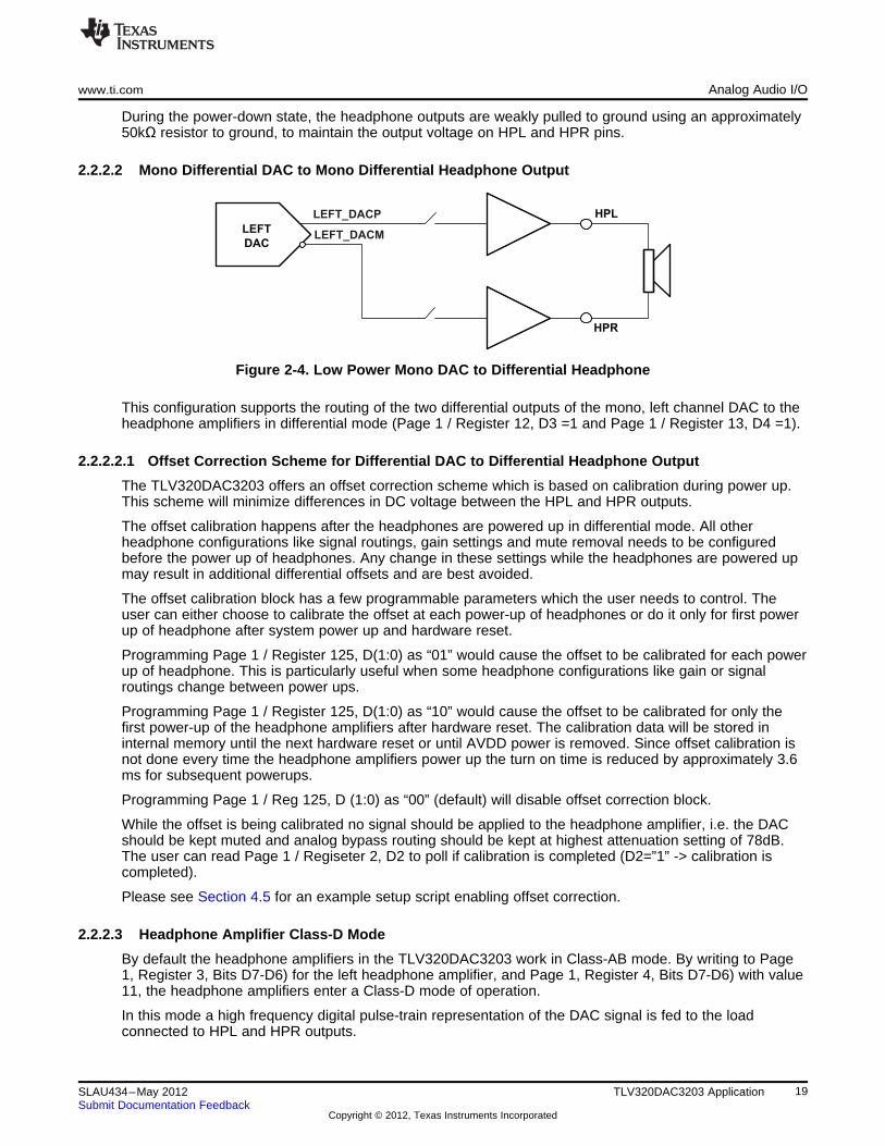
2.2.2.2 Mono Differential DAC to Mono Differential Headphone Output
Figure 2-4. Low Power Mono DAC to Differential Headphone
This configuration supports the routing of the two differential outputs of the mono, left channel DAC to theheadphone amplifiers in differential mode (Page 1 / Register 12, D3 =1 and Page 1 / Register 13, D4 =1).
2.2.2.2.1 Offset Correction Scheme for Differential DAC to Differential Headphone Output
The TLV320DAC3203 offers an offset correction scheme which is based on calibration during power up.This scheme will minimize differences in DC voltage between the HPL and HPR outputs.
The offset calibration happens after the headphones are powered up in differential mode. All otherheadphone configurations like signal routings, gain settings and mute removal needs to be configuredbefore the power up of headphones. Any change in these settings while the headphones are powered upmay result in additional differential offsets and are best avoided.
The offset calibration block has a few programmable parameters which the user needs to control. Theuser can either choose to calibrate the offset at each power-up of headphones or do it only for first powerup of headphone after system power up and hardware reset.
Programming Page 1 / Register 125, D(1:0) as “01” would cause the offset to be calibrated for each powerup of headphone. This is particularly useful when some headphone configurations like gain or signalroutings change between power ups.
Programming Page 1 / Register 125, D(1:0) as “10” would cause the offset to be calibrated for only thefirst power-up of the headphone amplifiers after hardware reset. The calibration data will be stored ininternal memory until the next hardware reset or until AVDD power is removed. Since offset calibration isnot done every time the headphone amplifiers power up the turn on time is reduced by approximately 3.6ms for subsequent powerups.
Programming Page 1 / Reg 125, D (1:0) as “00” (default) will disable offset correction block.
While the offset is being calibrated no signal should be applied to the headphone amplifier, i.e. the DACshould be kept muted and analog bypass routing should be kept at highest attenuation setting of 78dB.The user can read Page 1 / Regiseter 2, D2 to poll if calibration is completed (D2=”1” -> calibration iscompleted).
Please see Section 4.5 for an example setup script enabling offset correction.
2.2.2.3 Headphone Amplifier Class-D Mode
By default the headphone amplifiers in the TLV320DAC3203 work in Class-AB mode. By writing to Page1, Register 3, Bits D7-D6) for the left headphone amplifier, and Page 1, Register 4, Bits D7-D6) with value11, the headphone amplifiers enter a Class-D mode of operation.
In this mode a high frequency digital pulse-train representation of the DAC signal is fed to the loadconnected to HPL and HPR outputs.
19SLAU434–May 2012 TLV320DAC3203 ApplicationSubmit Documentation Feedback
Copyright © 2012, Texas Instruments Incorporated

L = 82 Hm C = 47 FC
m
C = 1 FmRload = 32 W
Analog Audio I/O www.ti.com
Because the output signal is a pulse train switching between Power Supply and Ground, the efficiency ofthe amplifier is greatly improved. In this mode however, for good noise performance, care should be takento keep the analog power supply clean.
For using the Class-D mode of operation, the following clock-divider condition should be met:
MDAC = I × 4, where I = 1, 2, ..., 32
When a direct digital pulse train is driven out as a signal, high frequencies as a function of pulse trainfrequency are also present which lead to power waste. To increase the efficiency and reduce powerdissipation in the load due to these high frequencies, an LC filter should be used in series with the outputand the load. The cutoff frequency of the LC filter should be adjusted to allow audio signals below 20kHzto pass through, but highly attenuate the high-frequency signal content.
Figure 2-5. Configuration for Using Headphone Amplifier in Class-D Mode
For using the headphones in the Class-D mode of operation, the headphones should first be powered upin default Class-AB mode to charge the AC-coupling capacitor to the set common mode voltage. Once theheadphone amplifiers have been so powered up, the DAC should be routed to headphones and unmutedbefore they can be switched to the Class-D mode. After Class D mode has been turned on, the linear,Class AB mode amplifier must be turned off. For powering down the headphone amplifiers, the DACshould first be muted.
See Section 4.3 for an example setup script enabling Class-D mode.
20 TLV320DAC3203 Application SLAU434–May 2012Submit Documentation Feedback
Copyright © 2012, Texas Instruments Incorporated

Left ADC
CIC filter
Right ADC
CIC filter
Signal
Processing
Blocks
GPIO
MISO
DIN
SCLK
DIG_MIC_IN
DIG_MIC_CLKTo dig. mic
CLK
From dig.
mic DATA
www.ti.com Digital Microphone Input/Decimation Filter
2.3 Digital Microphone Input/Decimation Filter
The TLV320DAC3203 includes a stereo decimation filter for digital microphone inputs. The stereorecording path can be powered up one channel at a time, to support the case where only mono recordcapability is required.
The digital microphone input path of the TLV320DAC3203 features a large set of options for signalconditioning as well as signal routing:
• Stereo decimation filters (PDM input)
• Fine gain adjustment of digital channels with 0.1 dB step size
• Digital volume control with a range of -12 to +20dB
• Mute function
In addition to the standard set of stereo decimation filter features the TLV320DAC3203 also offers thefollowing special functions:
• Channel-to-channel phase adjustment
• Adaptive filter mode
2.3.1 Digital Microphone Interface
The TLV320DAC3203 digital-microphone interface is shown in Figure 2-6.
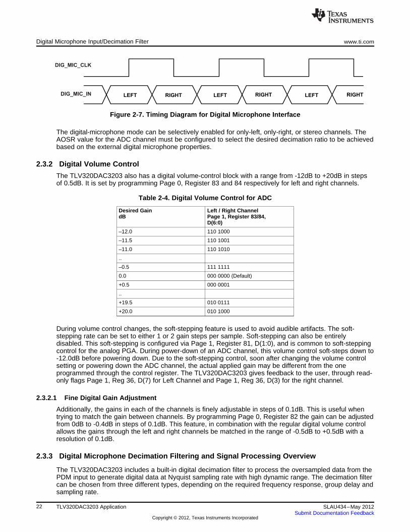
Figure 2-6. Digital Microphone in TLV320DAC3203
The TLV320DAC3203 outputs internal clock DIG_MIC_CLK on GPIO pin ( Page 0, Register 51, D(5:2)) orMISO pin (Page 0, Register 55, D(4:1)). This clock can be connected to the external digital microphonedevice. The single-bit output of the external digital microphone device can be connected to GPIO, DIN orSCLK pins. Internally the TLV320DAC3203 latches the steady value of data on the rising edge ofDIG_MIC_CLK for the Left ADC channel, and the steady value of data on falling edge for the Right ADCchannel.
21SLAU434–May 2012 TLV320DAC3203 ApplicationSubmit Documentation Feedback
Copyright © 2012, Texas Instruments Incorporated
LEFT RIGHT LEFT RIGHT LEFT RIGHT
DIG_MIC_CLK
DIG_MIC_IN
Digital Microphone Input/Decimation Filter www.ti.com
Figure 2-7. Timing Diagram for Digital Microphone Interface
The digital-microphone mode can be selectively enabled for only-left, only-right, or stereo channels. TheAOSR value for the ADC channel must be configured to select the desired decimation ratio to be achievedbased on the external digital microphone properties.
2.3.2 Digital Volume Control
The TLV320DAC3203 also has a digital volume-control block with a range from -12dB to +20dB in stepsof 0.5dB. It is set by programming Page 0, Register 83 and 84 respectively for left and right channels.
Table 2-4. Digital Volume Control for ADC
Desired Gain Left / Right ChanneldB Page 1, Register 83/84,
D(6:0)
–12.0 110 1000
–11.5 110 1001
–11.0 110 1010
..
–0.5 111 1111
0.0 000 0000 (Default)
+0.5 000 0001
..
+19.5 010 0111
+20.0 010 1000
During volume control changes, the soft-stepping feature is used to avoid audible artifacts. The soft-stepping rate can be set to either 1 or 2 gain steps per sample. Soft-stepping can also be entirelydisabled. This soft-stepping is configured via Page 1, Register 81, D(1:0), and is common to soft-steppingcontrol for the analog PGA. During power-down of an ADC channel, this volume control soft-steps down to-12.0dB before powering down. Due to the soft-stepping control, soon after changing the volume controlsetting or powering down the ADC channel, the actual applied gain may be different from the oneprogrammed through the control register. The TLV320DAC3203 gives feedback to the user, through read-only flags Page 1, Reg 36, D(7) for Left Channel and Page 1, Reg 36, D(3) for the right channel.
2.3.2.1 Fine Digital Gain Adjustment
Additionally, the gains in each of the channels is finely adjustable in steps of 0.1dB. This is useful whentrying to match the gain between channels. By programming Page 0, Register 82 the gain can be adjustedfrom 0dB to -0.4dB in steps of 0.1dB. This feature, in combination with the regular digital volume controlallows the gains through the left and right channels be matched in the range of -0.5dB to +0.5dB with aresolution of 0.1dB.
2.3.3 Digital Microphone Decimation Filtering and Signal Processing Overview
The TLV320DAC3203 includes a built-in digital decimation filter to process the oversampled data from thePDM input to generate digital data at Nyquist sampling rate with high dynamic range. The decimation filtercan be chosen from three different types, depending on the required frequency response, group delay andsampling rate.
22 TLV320DAC3203 Application SLAU434–May 2012Submit Documentation Feedback
Copyright © 2012, Texas Instruments Incorporated

www.ti.com Digital Microphone Input/Decimation Filter
Processing Blocks
The TLV320DAC3203 offers a range of processing blocks which implement various signal processingcapabilities along with decimation filtering. These processing blocks give users the choice of how muchand what type of signal processing they may use and which decimation filter is applied.
Table 2-5 gives an overview of the available processing blocks and their properties.
The signal processing blocks available are:
• First-order IIR
• Scalable number of biquad filters
• Variable-tap FIR filter
The processing blocks are tuned for common cases and can achieve high anti-alias filtering or low-groupdelay in combination with various signal processing effects such as audio effects and frequency shaping.The available first order IIR, BiQuad and FIR filters have fully user-programmable coefficients. TheResource Class Column (RC) gives an approximate indication of power consumption.
Table 2-5. Processing Blocks
Processing Channel Decimation 1st Order Number FIR Required ResourceBlocks Filter IIR BiQuads AOSR Value Class
Available
PRB_R1 (1) Stereo A Yes 0 No 128,64 6
PRB_R2 Stereo A Yes 5 No 128,64 8
PRB_R3 Stereo A Yes 0 25-Tap 128,64 8
PRB_R4 Right A Yes 0 No 128,64 3
PRB_R5 Right A Yes 5 No 128,64 4
PRB_R6 Right A Yes 0 25-Tap 128,64 4
PRB_R7 Stereo B Yes 0 No 64 3
PRB_R8 Stereo B Yes 3 No 64 4
PRB_R9 Stereo B Yes 0 20-Tap 64 4
PRB_R10 Right B Yes 0 No 64 2
PRB_R11 Right B Yes 3 No 64 2
PRB_R12 Right B Yes 0 20-Tap 64 2
PRB_R13 Stereo C Yes 0 No 32 3
PRB_R14 Stereo C Yes 5 No 32 4
PRB_R15 Stereo C Yes 0 25-Tap 32 4
PRB_R16 Right C Yes 0 No 32 2
PRB_R17 Right C Yes 5 No 32 2
PRB_R18 Right C Yes 0 25-Tap 32 2(1) Default
23SLAU434–May 2012 TLV320DAC3203 ApplicationSubmit Documentation Feedback
Copyright © 2012, Texas Instruments Incorporated

To AudioInterface
1st
OrderIIRFilter B
FromDigital Vol. Ctrl
´
From CICFilter
1st
OrderIIRFilter A 25-Tap FIR
FromDigital Vol. Ctrl
To Audio
Interface´
From CICFilter
1st
Order
IIRFilter A H E
H DH CHBH ATo Audio
Interface
FromDigital Vol. Ctrl
´From CIC
Filter
To AudioInterface
1st
OrderIIR´Filter A
From CICFilter
FromDigital Vol. Ctrl
Digital Microphone Input/Decimation Filter www.ti.com
2.3.3.1 Signal Processing Details
2.3.3.1.1 Processing Block Descriptions
2.3.3.1.1.1 1st order IIR, Filter A
Figure 2-8. Signal Chain for PRB_R1 and PRB_R4
2.3.3.1.1.2 5 Biquads, 1st order IIR, Filter A
Figure 2-9. Signal Chain PRB_R2 and PRB_R5
2.3.3.1.1.3 25 Tap FIR, 1st order IIR, Filter A
Figure 2-10. Signal Chain for PRB_R3 and PRB_R6
2.3.3.1.1.4 1st order IIR, Filter B
Figure 2-11. Signal Chain for PRB_R7 and PRB_R10
24 TLV320DAC3203 Application SLAU434–May 2012Submit Documentation Feedback
Copyright © 2012, Texas Instruments Incorporated
1st
OrderIIR
Filter C H EH DH CHBH A
FromDigital Vol. Ctrl
To Audio
Interface´From CIC
Filter
1st
OrderIIRFilter C
FromDigital Vol. Ctrl
To AudioInterface
´
From CICFilter
1st OrderIIRFilter B 20-Tap FIR
From
To Audio
Interface´
From CICFilter
1st
OrderIIR
Filter B HCHBHA
FromDigital Vol. Ctrl
To Audio
Interface´From CIC
Filter
www.ti.com Digital Microphone Input/Decimation Filter
2.3.3.1.1.5 3 Biquads, 1st order IIR, Filter B
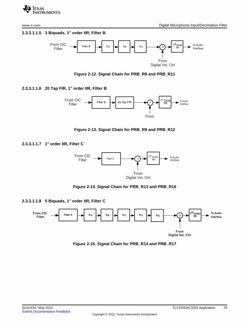
Figure 2-12. Signal Chain for PRB_R8 and PRB_R11
2.3.3.1.1.6 20 Tap FIR, 1st order IIR, Filter B
Figure 2-13. Signal Chain for PRB_R9 and PRB_R12
2.3.3.1.1.7 1st order IIR, Filter C
Figure 2-14. Signal Chain for PRB_R13 and PRB_R16
2.3.3.1.1.8 5 Biquads, 1st order IIR, Filter C
Figure 2-15. Signal Chain for PRB_R14 and PRB_R17
25SLAU434–May 2012 TLV320DAC3203 ApplicationSubmit Documentation Feedback
Copyright © 2012, Texas Instruments Incorporated
1st
OrderIIRFilter C 25-Tap FIR
FromDigital Vol. Ctrl
To Audio
Interface´
From CICFilter
Digital Microphone Input/Decimation Filter www.ti.com
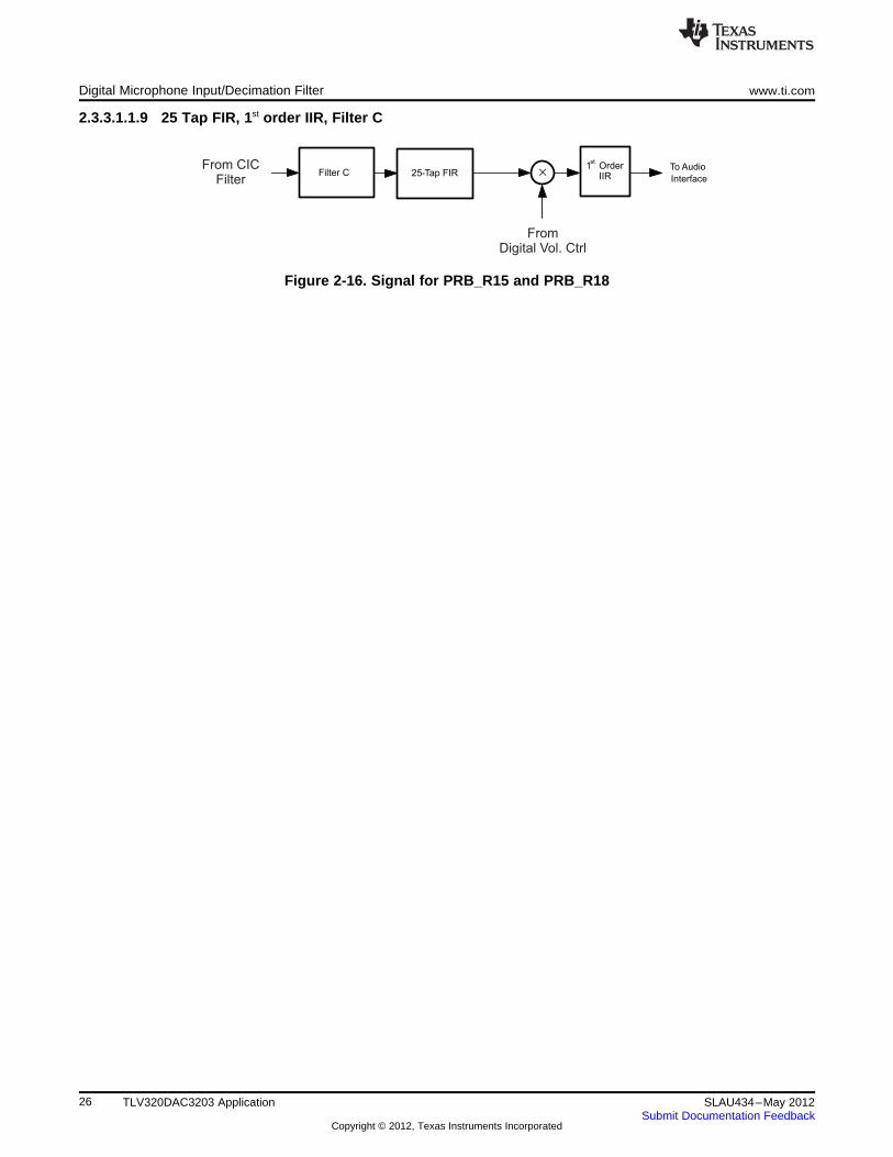
2.3.3.1.1.9 25 Tap FIR, 1st order IIR, Filter C
Figure 2-16. Signal for PRB_R15 and PRB_R18
26 TLV320DAC3203 Application SLAU434–May 2012Submit Documentation Feedback
Copyright © 2012, Texas Instruments Incorporated
1
1
23
1
10
zD2
zNN)z(H
-
-
-
+
=
www.ti.com Digital Microphone Input/Decimation Filter
2.3.3.1.2 User Programmable Filters
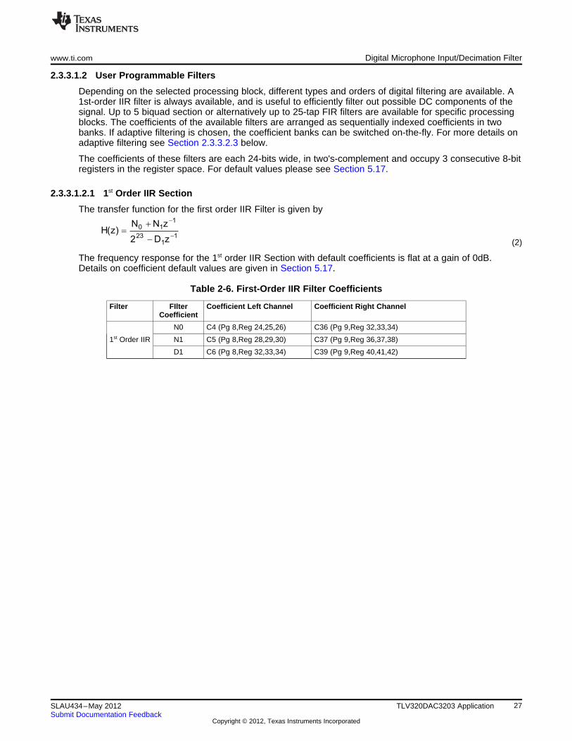
Depending on the selected processing block, different types and orders of digital filtering are available. A1st-order IIR filter is always available, and is useful to efficiently filter out possible DC components of thesignal. Up to 5 biquad section or alternatively up to 25-tap FIR filters are available for specific processingblocks. The coefficients of the available filters are arranged as sequentially indexed coefficients in twobanks. If adaptive filtering is chosen, the coefficient banks can be switched on-the-fly. For more details onadaptive filtering see Section 2.3.3.2.3 below.
The coefficients of these filters are each 24-bits wide, in two's-complement and occupy 3 consecutive 8-bitregisters in the register space. For default values please see Section 5.17.
2.3.3.1.2.1 1st Order IIR Section
The transfer function for the first order IIR Filter is given by
(2)
The frequency response for the 1st order IIR Section with default coefficients is flat at a gain of 0dB.Details on coefficient default values are given in Section 5.17.
Table 2-6. First-Order IIR Filter Coefficients
Filter FIlter Coefficient Left Channel Coefficient Right ChannelCoefficient
N0 C4 (Pg 8,Reg 24,25,26) C36 (Pg 9,Reg 32,33,34)
1st Order IIR N1 C5 (Pg 8,Reg 28,29,30) C37 (Pg 9,Reg 36,37,38)
D1 C6 (Pg 8,Reg 32,33,34) C39 (Pg 9,Reg 40,41,42)
27SLAU434–May 2012 TLV320DAC3203 ApplicationSubmit Documentation Feedback
Copyright © 2012, Texas Instruments Incorporated

2
2
1
1
23
2
2
1
10
zDzD*22
zNzN*2N)z(H
--
--
--
++
=
Digital Microphone Input/Decimation Filter www.ti.com
2.3.3.1.2.2 Biquad Section
The transfer function of each of the Biquad Filters is given by
(3)
The frequency response for each of the biquad section with default coefficients is flat at a gain of 0dB.Details on coefficient default values are given in Section 5.17.
Table 2-7. Biquad Filter Coefficients
Filter FIlter Coefficient Left Channel Coefficient Right ChannelCoefficient
BIQUAD A N0 C7 (Pg 8, Reg 36,37,38) C39 (Pg 9, Reg 44,45,46)
N1 C8 (Pg 8, Reg 40,41,42) C40 (Pg 9, Reg 48,49,50)
N2 C9 (Pg 8, Reg 44,45,46) C41 (Pg 9, Reg 52,53,54)
D1 C10 (Pg 8, Reg 48,49,50) C42 (Pg 9, Reg 56,57,58)
D2 C11 (Pg 8, Reg 52,53,54) C43 (Pg 9, Reg 60,61,62)
BIQUAD B N0 C12 (Pg 8, Reg 56,57,58) C44 (Pg 9, Reg 64,65,66)
N1 C13 (Pg 8, Reg 60,61,62) C45 (Pg 9, Reg 68,69,70)
N2 C14 (Pg 8, Reg 64,65,66) C46 (Pg 9, Reg 72,73,74)
D1 C15 (Pg 8, Reg 68,69,70) C47 (Pg 9, Reg 76,77,78)
D2 C16 (Pg 8, Reg 72,73,74) C48 (Pg 9, Reg 80,81,82)
BIQUAD C N0 C17 (Pg 8, Reg 76,77,78) C49 (Pg 9, Reg 84,85,86)
N1 C18 (Pg 8, Reg 80,81,82) C50 (Pg 9, Reg 88,89,90)
N2 C19 (Pg 8, Reg 84,85,86) C51 (Pg 9, Reg 92,93,94)
D1 C20 (Pg 8, Reg 88,89,90) C52 (Pg 9, Reg 96,97,98)
D2 C21 (Pg 8, Reg 92,93,94) C53 (Pg 9, Reg 100,101,102)
BIQUAD D N0 C22 (Pg 8, Reg 96,97,98) C54 (Pg 9, Reg 104,105,106)
N1 C23 (Pg 8, Reg 100,101,102) C55 (Pg 9, Reg 108,109,110)
N2 C24 (Pg 8, Reg 104,105,106) C56 (Pg 9, Reg 112,113,114)
D1 C25 (Pg 8, Reg 108,109,110) C57 (Pg 9, Reg 116,117,118)
D2 C26 (Pg 8, Reg 112,113,114) C58 (Pg 9, Reg 120,121,122)
BIQUAD E N0 C27 (Pg 8, Reg 116,117,118) C59 (Pg 9, Reg 124,125,126)
N1 C28 (Pg 8, Reg 120,121,122) C60 (Pg 10, Reg 8,9,10)
N2 C29 (Pg 8, Reg 124,125,126) C61 (Pg 10, Reg 12,13,14)
D1 C30 (Pg 9, Reg 8,9,10) C62 (Pg 10, Reg 16,17,18)
D2 C31 (Pg 9, Reg 12,13,14) C63 (Pg 10, Reg 20,21,22)
28 TLV320DAC3203 Application SLAU434–May 2012Submit Documentation Feedback
Copyright © 2012, Texas Instruments Incorporated
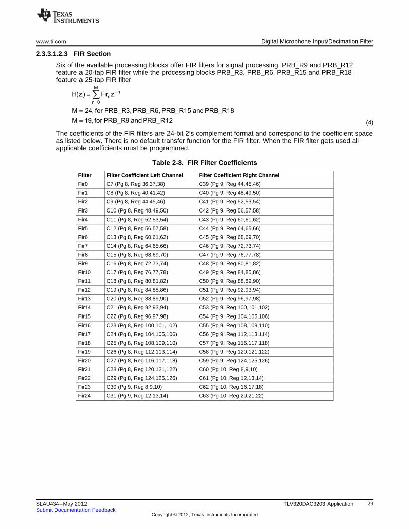
PRB_R12andPRB_R9for,19M
PRB_R18andPRB_R15PRB_R6,PRB_R3,for,24M
zFir)z(H
M
0n
n
n
=
=
= å=
-
www.ti.com Digital Microphone Input/Decimation Filter
2.3.3.1.2.3 FIR Section
Six of the available processing blocks offer FIR filters for signal processing. PRB_R9 and PRB_R12feature a 20-tap FIR filter while the processing blocks PRB_R3, PRB_R6, PRB_R15 and PRB_R18feature a 25-tap FIR filter
(4)
The coefficients of the FIR filters are 24-bit 2’s complement format and correspond to the coefficient spaceas listed below. There is no default transfer function for the FIR filter. When the FIR filter gets used allapplicable coefficients must be programmed.
Table 2-8. FIR Filter Coefficients
Filter FIlter Coefficient Left Channel Filter Coefficient Right Channel
Fir0 C7 (Pg 8, Reg 36,37,38) C39 (Pg 9, Reg 44,45,46)
Fir1 C8 (Pg 8, Reg 40,41,42) C40 (Pg 9, Reg 48,49,50)
Fir2 C9 (Pg 8, Reg 44,45,46) C41 (Pg 9, Reg 52,53,54)
Fir3 C10 (Pg 8, Reg 48,49,50) C42 (Pg 9, Reg 56,57,58)
Fir4 C11 (Pg 8, Reg 52,53,54) C43 (Pg 9, Reg 60,61,62)
Fir5 C12 (Pg 8, Reg 56,57,58) C44 (Pg 9, Reg 64,65,66)
Fir6 C13 (Pg 8, Reg 60,61,62) C45 (Pg 9, Reg 68,69,70)
Fir7 C14 (Pg 8, Reg 64,65,66) C46 (Pg 9, Reg 72,73,74)
Fir8 C15 (Pg 8, Reg 68,69,70) C47 (Pg 9, Reg 76,77,78)
Fir9 C16 (Pg 8, Reg 72,73,74) C48 (Pg 9, Reg 80,81,82)
Fir10 C17 (Pg 8, Reg 76,77,78) C49 (Pg 9, Reg 84,85,86)
Fir11 C18 (Pg 8, Reg 80,81,82) C50 (Pg 9, Reg 88,89,90)
Fir12 C19 (Pg 8, Reg 84,85,86) C51 (Pg 9, Reg 92,93,94)
Fir13 C20 (Pg 8, Reg 88,89,90) C52 (Pg 9, Reg 96,97,98)
Fir14 C21 (Pg 8, Reg 92,93,94) C53 (Pg 9, Reg 100,101,102)
Fir15 C22 (Pg 8, Reg 96,97,98) C54 (Pg 9, Reg 104,105,106)
Fir16 C23 (Pg 8, Reg 100,101,102) C55 (Pg 9, Reg 108,109,110)
Fir17 C24 (Pg 8, Reg 104,105,106) C56 (Pg 9, Reg 112,113,114)
Fir18 C25 (Pg 8, Reg 108,109,110) C57 (Pg 9, Reg 116,117,118)
Fir19 C26 (Pg 8, Reg 112,113,114) C58 (Pg 9, Reg 120,121,122)
Fir20 C27 (Pg 8, Reg 116,117,118) C59 (Pg 9, Reg 124,125,126)
Fir21 C28 (Pg 8, Reg 120,121,122) C60 (Pg 10, Reg 8,9,10)
Fir22 C29 (Pg 8, Reg 124,125,126) C61 (Pg 10, Reg 12,13,14)
Fir23 C30 (Pg 9, Reg 8,9,10) C62 (Pg 10, Reg 16,17,18)
Fir24 C31 (Pg 9, Reg 12,13,14) C63 (Pg 10, Reg 20,21,22)
29SLAU434–May 2012 TLV320DAC3203 ApplicationSubmit Documentation Feedback
Copyright © 2012, Texas Instruments Incorporated
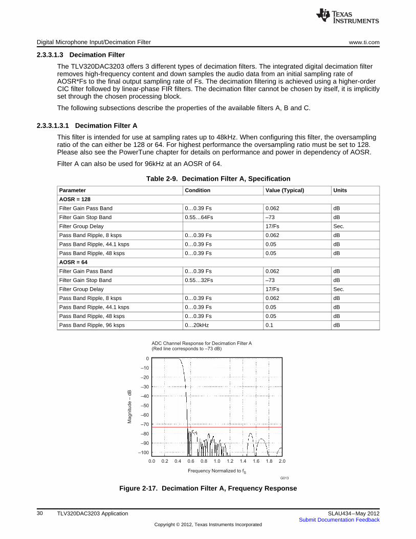
0
–10
–20
–30
–40
–50
–60
–70
–80
–90
–100
0.0 0.2 0.4 0.6 0.8 1.0 1.2 1.4 1.6 1.8 2.0
Frequency Normalized to fS
Magnitude
–dB
ADC Channel Response for Decimation Filter A(Red line corresponds to –73 dB)
G013
Digital Microphone Input/Decimation Filter www.ti.com
2.3.3.1.3 Decimation Filter
The TLV320DAC3203 offers 3 different types of decimation filters. The integrated digital decimation filterremoves high-frequency content and down samples the audio data from an initial sampling rate ofAOSR*Fs to the final output sampling rate of Fs. The decimation filtering is achieved using a higher-orderCIC filter followed by linear-phase FIR filters. The decimation filter cannot be chosen by itself, it is implicitlyset through the chosen processing block.
The following subsections describe the properties of the available filters A, B and C.
2.3.3.1.3.1 Decimation Filter A
This filter is intended for use at sampling rates up to 48kHz. When configuring this filter, the oversamplingratio of the can either be 128 or 64. For highest performance the oversampling ratio must be set to 128.Please also see the PowerTune chapter for details on performance and power in dependency of AOSR.
Filter A can also be used for 96kHz at an AOSR of 64.
Table 2-9. Decimation Filter A, Specification
Parameter Condition Value (Typical) Units
AOSR = 128
Filter Gain Pass Band 0…0.39 Fs 0.062 dB
Filter Gain Stop Band 0.55…64Fs –73 dB
Filter Group Delay 17/Fs Sec.
Pass Band Ripple, 8 ksps 0…0.39 Fs 0.062 dB
Pass Band Ripple, 44.1 ksps 0…0.39 Fs 0.05 dB
Pass Band Ripple, 48 ksps 0…0.39 Fs 0.05 dB
AOSR = 64
Filter Gain Pass Band 0…0.39 Fs 0.062 dB
Filter Gain Stop Band 0.55…32Fs –73 dB
Filter Group Delay 17/Fs Sec.
Pass Band Ripple, 8 ksps 0…0.39 Fs 0.062 dB
Pass Band Ripple, 44.1 ksps 0…0.39 Fs 0.05 dB
Pass Band Ripple, 48 ksps 0…0.39 Fs 0.05 dB
Pass Band Ripple, 96 ksps 0…20kHz 0.1 dB
Figure 2-17. Decimation Filter A, Frequency Response
30 TLV320DAC3203 Application SLAU434–May 2012Submit Documentation Feedback
Copyright © 2012, Texas Instruments Incorporated
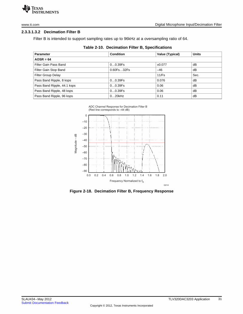
0
–10
–20
–30
–40
–50
–60
–70
–80
–90
0.0 0.2 0.4 0.6 0.8 1.0 1.2 1.4 1.6 1.8 2.0
Frequency Normalized to fS
Magnitude
–dB
ADC Channel Response for Decimation Filter B(Red line corresponds to –44 dB)
G014
www.ti.com Digital Microphone Input/Decimation Filter
2.3.3.1.3.2 Decimation Filter B
Filter B is intended to support sampling rates up to 96kHz at a oversampling ratio of 64.
Table 2-10. Decimation Filter B, Specifications
Parameter Condition Value (Typical) Units
AOSR = 64
Filter Gain Pass Band 0…0.39Fs ±0.077 dB
Filter Gain Stop Band 0.60Fs…32Fs –46 dB
Filter Group Delay 11/Fs Sec.
Pass Band Ripple, 8 ksps 0…0.39Fs 0.076 dB
Pass Band Ripple, 44.1 ksps 0…0.39Fs 0.06 dB
Pass Band Ripple, 48 ksps 0…0.39Fs 0.06 dB
Pass Band Ripple, 96 ksps 0…20kHz 0.11 dB
Figure 2-18. Decimation Filter B, Frequency Response
31SLAU434–May 2012 TLV320DAC3203 ApplicationSubmit Documentation Feedback
Copyright © 2012, Texas Instruments Incorporated

ADC Channel Response for Decimation Filter C(Red line corresponds to –60 dB)
0
–20
–40
–60
–100
–80
–120
0.0 0.2 0.4 0.6 0.8 1.0 1.2 1.4 1.6 1.8 2.0
Frequency Normalized to fS
Magnitude
–dB
G015
Digital Microphone Input/Decimation Filter www.ti.com
2.3.3.1.3.3 Decimation Filter C
Filter type C along with AOSR of 32 is specially designed for 192ksps operation for the ADC. The passband which extends up to 0.11*Fs ( corresponds to 21kHz), is suited for audio applications.
Table 2-11. Decimation Filter C, Specifications
Parameter Condition Value (Typical) Units
Filter Gain from 0 to 0.11Fs 0…0.11Fs ±0.033 dB
Filter Gain from 0.28Fs to 16Fs 0.28Fs…16Fs –60 dB
Filter Group Delay 11/Fs Sec.
Pass Band Ripple, 8 ksps 0…0.11Fs 0.033 dB
Pass Band Ripple, 44.1 ksps 0…0.11Fs 0.033 dB
Pass Band Ripple, 48 ksps 0…0.11Fs 0.032 dB
Pass Band Ripple, 96 ksps 0…0.11Fs 0.032 dB
Pass Band Ripple, 192 ksps 0…20kHz 0.086 dB
Figure 2-19. Decimation Filter C, Frequency Response
2.3.3.1.4 ADC Data Interface
The decimation filter and signal processing block in the ADC channel passes 32-bit data words to theaudio serial interface once every cycle of Fs,ADC. During each cycle of Fs,ADC, a pair of data words ( forleft and right channel ) are passed. The audio serial interface rounds the data to the required word lengthof the interface before converting to serial data as per the different modes for audio serial interface.
32 TLV320DAC3203 Application SLAU434–May 2012Submit Documentation Feedback
Copyright © 2012, Texas Instruments Incorporated

FS_ADC*AOSR
)7(Delaytpl =
)tt(OUT_ADC_LEFT)t(COMP_PHASE_ADC_LEFT pl-=
( )
FS_ADC*AOSR
k*AOSR*)5:6(Delay)0:4(Delayt fpr
+
=
)tt(OUT_ADC_RIGHT)t(COMP_PHASE_ADC_RIGHT pr-=
www.ti.com Digital Microphone Input/Decimation Filter
2.3.3.2 Special Functions
2.3.3.2.1 Microphone Bias
The TLV320DAC3203 has a built-in low noise Microphone Bias support for electret-condensermicrophones. The Bias amplifier can support up to 3mA of load current to support multiple microphones.The Bias amplifier has been designed to provide a combination of high PSRR, low noise andprogrammable bias voltages to allow the user to fine tune the biasing to specific microphonecombinations. To support a wide range of bias voltages, the bias amplifier can work of either a low analogsupply or high LDOIN supply.
Table 2-12. MICBIAS Voltage Control
Page 1, Reg 51, D(5:4) Page 1, Reg 10, D(6) Page 1, Reg 51, D(3) MICBIAS Voltage (without load)
00 0 X 1.25V
00 1 X 1.0V
01 0 X 1.7V
01 1 X 1.4V
10 0 1 2.5V
10 1 1 2.1V
11 X 0 AVdd
11 X 1 LDOIN
2.3.3.2.2 Channel-to-Channel Phase Adjustment
The TLV320DAC3203 has a built-in feature to fine-adjust the phase between the stereo ADC recordsignals. The phase compensation is particularly helpful to adjust delays when using dual microphones fornoise cancellation etc.
This delay can be controlled in fine amounts in the following fashion.
Delay(7:0) = Page 0/Register 85/D(7:0)
Where
(5)
where
(6)
Where kf is a function of the decimation filter:
Decimation Filter Type kf
A 0.25
B 0.5
C 1
and
(7)
Where
(8)
33SLAU434–May 2012 TLV320DAC3203 ApplicationSubmit Documentation Feedback
Copyright © 2012, Texas Instruments Incorporated
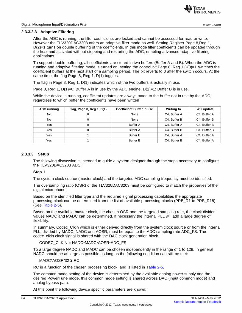
Digital Microphone Input/Decimation Filter www.ti.com
2.3.3.2.3 Adaptive Filtering
After the ADC is running, the filter coefficients are locked and cannot be accessed for read or write.However the TLV320DAC3203 offers an adaptive filter mode as well. Setting Register Page 8,Reg 1,D(2)=1 turns on double buffering of the coefficients. In this mode filter coefficients can be updated throughthe host and activated without stopping and restarting the ADC, enabling advanced adaptive filteringapplications.
To support double buffering, all coefficients are stored in two buffers (Buffer A and B). When the ADC isrunning and adaptive filtering mode is turned on, setting the control bit Page 8, Reg 1,D(0)=1 switches thecoefficient buffers at the next start of a sampling period. The bit reverts to 0 after the switch occurs. At thesame time, the flag Page 8, Reg 1, D(1) toggles.
The flag in Page 8, Reg 1, D(1) indicates which of the two buffers is actually in use.
Page 8, Reg 1, D(1)=0: Buffer A is in use by the ADC engine, D(1)=1: Buffer B is in use.
While the device is running, coefficient updates are always made to the buffer not in use by the ADC,regardless to which buffer the coefficients have been written
ADC running Flag, Page 8, Reg 1, D(1) Coefficient Buffer in use Writing to Will update
No 0 None C4, Buffer A C4, Buffer A
No 0 None C4, Buffer B C4, Buffer B
Yes 0 Buffer A C4, Buffer A C4, Buffer B
Yes 0 Buffer A C4, Buffer B C4, Buffer B
Yes 1 Buffer B C4, Buffer A C4, Buffer A
Yes 1 Buffer B C4, Buffer B C4, Buffer A
2.3.3.3 Setup
The following discussion is intended to guide a system designer through the steps necessary to configurethe TLV320DAC3203 ADC.
Step 1
The system clock source (master clock) and the targeted ADC sampling frequency must be identified.
The oversampling ratio (OSR) of the TLV320DAC3203 must be configured to match the properties of thedigital microphone.
Based on the identified filter type and the required signal processing capabilities the appropriateprocessing block can be determined from the list of available processing blocks (PRB_R1 to PRB_R18)(See Table 2-5).
Based on the available master clock, the chosen OSR and the targeted sampling rate, the clock dividervalues NADC and MADC can be determined. If necessary the internal PLL will add a large degree offlexibility.
In summary, Codec_Clkin which is either derived directly from the system clock source or from the internalPLL, divided by MADC, NADC and AOSR, must be equal to the ADC sampling rate ADC_FS. Thecodec_clkin clock signal is shared with the DAC clock generation block.
CODEC_CLKIN = NADC*MADC*AOSR*ADC_FS
To a large degree NADC and MADC can be chosen independently in the range of 1 to 128. In generalNADC should be as large as possible as long as the following condition can still be met:
MADC*AOSR/32 ≥ RC
RC is a function of the chosen processing block, and is listed in Table 2-5.
The common mode setting of the device is determined by the available analog power supply and thedesired PowerTune mode, this common mode setting is shared across DAC (input common mode) andanalog bypass path.
At this point the following device specific parameters are known:
34 TLV320DAC3203 Application SLAU434–May 2012Submit Documentation Feedback
Copyright © 2012, Texas Instruments Incorporated

www.ti.com DAC
PRB_Rx, AOSR, NADC, MADC, common mode setting
Additionally if the PLL is used the PLL parameters P, J, D and R are determined as well.
Step 2
Setting up the device via register programming:
The following list gives a sequence of items that must be executed between powering the device up andreading data from the device:
Define starting point: Set register page to 0Initiate SW Reset
Program Clock Settings Program PLL clock dividers P,J,D,R (if PLL is necessary)Power up PLL (if PLL is necessary)Program and power up NADCProgram and power up MADCProgram OSR valueProgram the processing block to be used
At this point, at the latest, analog power supply must be applied to the device (via internal LDO orexternal)
Program Analog Blocks Set register Page to 1Disable coarse AVdd generationEnable Master Analog Power Control
A detailed example can be found in Chapter 4.
2.4 DAC
The TLV320DAC3203 includes a stereo audio DAC supporting data rates from 8kHz to 192kHz. Eachchannel of the stereo audio DAC consists of a signal-processing engine with fixed processing blocks, adigital interpolation filter, multi-bit digital delta-sigma modulator, and an analog reconstruction filter. TheDAC is designed to provide enhanced performance at low sampling rates through increased oversamplingand image filtering, thereby keeping quantization noise generated within the delta-sigma modulator andsignal images strongly suppressed within the audio band to beyond 20kHz. To handle multiple input ratesand optimize performance, the TLV320DAC3203 allows the system designer to program the oversamplingrates over a wide range from 1 to 1024. The system designer can choose higher oversampling ratios forlower input data rates and lower oversampling ratios for higher input data rates.
The TLV320DAC3203 DAC channel includes a built-in digital interpolation filter to generate oversampleddata for the sigma-delta modulator. The interpolation filter can be chosen from three different typesdepending on required frequency response, group delay and sampling rate.
The DAC path of the TLV320DAC3203 features many options for signal conditioning and signal routing:
• Digital volume control with a range of -63.5 to +24dB
• Mute function
• Dynamic range compression (DRC)
In addition to the standard set of DAC features the TLV320DAC3203 also offers the following specialfeatures:
• Built in sine wave generation (beep generator)
• Digital auto mute
• Adaptive filter mode
The TLV320DAC3203 implements signal processing capabilities and interpolation filtering via processingblocks. These fixed processing blocks give users the choice of how much and what type of signalprocessing they may use and which interpolation filter is applied.
Table 2-13 gives an overview over all available processing blocks of the DAC channel and theirproperties.
35SLAU434–May 2012 TLV320DAC3203 ApplicationSubmit Documentation Feedback
Copyright © 2012, Texas Instruments Incorporated
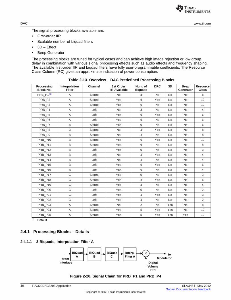
Interp.
Filter A
BiQuad
C
BiQuad
B
BiQuad
Ato
Modulator
Digital
Volume
Ctrl
from
Interface
´
DAC www.ti.com
The signal processing blocks available are:
• First-order IIR
• Scalable number of biquad filters
• 3D – Effect
• Beep Generator
The processing blocks are tuned for typical cases and can achieve high image rejection or low groupdelay in combination with various signal processing effects such as audio effects and frequency shaping.The available first-order IIR and biquad filters have fully user-programmable coefficients. The ResourceClass Column (RC) gives an approximate indication of power consumption.
Table 2-13. Overview – DAC Predefined Processing Blocks
Processing Interpolation Channel 1st Order Num. of DRC 3D Beep ResourceBlock No. Filter IIR Available Biquads Generator Class
PRB_P1 (1) A Stereo No 3 No No No 8
PRB_P2 A Stereo Yes 6 Yes No No 12
PRB_P3 A Stereo Yes 6 No No No 10
PRB_P4 A Left No 3 No No No 4
PRB_P5 A Left Yes 6 Yes No No 6
PRB_P6 A Left Yes 6 No No No 6
PRB_P7 B Stereo Yes 0 No No No 6
PRB_P8 B Stereo No 4 Yes No No 8
PRB_P9 B Stereo No 4 No No No 8
PRB_P10 B Stereo Yes 6 Yes No No 10
PRB_P11 B Stereo Yes 6 No No No 8
PRB_P12 B Left Yes 0 No No No 3
PRB_P13 B Left No 4 Yes No No 4
PRB_P14 B Left No 4 No No No 4
PRB_P15 B Left Yes 6 Yes No No 6
PRB_P16 B Left Yes 6 No No No 4
PRB_P17 C Stereo Yes 0 No No No 3
PRB_P18 C Stereo Yes 4 Yes No No 6
PRB_P19 C Stereo Yes 4 No No No 4
PRB_P20 C Left Yes 0 No No No 2
PRB_P21 C Left Yes 4 Yes No No 3
PRB_P22 C Left Yes 4 No No No 2
PRB_P23 A Stereo No 2 No Yes No 8
PRB_P24 A Stereo Yes 5 Yes Yes No 12
PRB_P25 A Stereo Yes 5 Yes Yes Yes 12(1) Default
2.4.1 Processing Blocks – Details
2.4.1.1 3 Biquads, Interpolation Filter A
Figure 2-20. Signal Chain for PRB_P1 and PRB_P4
36 TLV320DAC3203 Application SLAU434–May 2012Submit Documentation Feedback
Copyright © 2012, Texas Instruments Incorporated
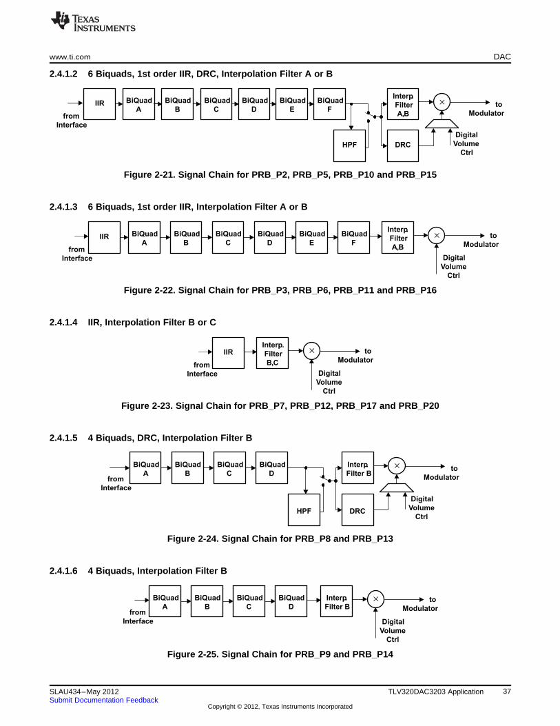
Interp.
Filter B
BiQuad
D
BiQuad
C
BiQuad
B
BiQuad
Ato
Modulator
Digital
Volume
Ctrl
from
Interface
´
Interp.
Filter B
DRCHPF
to
Modulator
Digital
Volume
Ctrl
BiQuad
D
BiQuad
C
BiQuad
B
BiQuad
Afrom
Interface
´
Interp.
Filter
B,C
IIR to
Modulator
Digital
Volume
Ctrl
from
Interface
´
Interp.
Filter
A,B
BiQuad
F
BiQuad
E
BiQuad
D
BiQuad
C
BiQuad
B
BiQuad
AIIR to
Modulator
Digital
Volume
Ctrl
from
Interface
´
Interp.
Filter
A,B
DRCHPF
BiQuad
F
BiQuad
E
BiQuad
D
BiQuad
C
BiQuad
B
BiQuad
AIIR to
Modulator
Digital
Volume
Ctrl
from
Interface
´
www.ti.com DAC
2.4.1.2 6 Biquads, 1st order IIR, DRC, Interpolation Filter A or B
Figure 2-21. Signal Chain for PRB_P2, PRB_P5, PRB_P10 and PRB_P15
2.4.1.3 6 Biquads, 1st order IIR, Interpolation Filter A or B
Figure 2-22. Signal Chain for PRB_P3, PRB_P6, PRB_P11 and PRB_P16
2.4.1.4 IIR, Interpolation Filter B or C
Figure 2-23. Signal Chain for PRB_P7, PRB_P12, PRB_P17 and PRB_P20
2.4.1.5 4 Biquads, DRC, Interpolation Filter B
Figure 2-24. Signal Chain for PRB_P8 and PRB_P13
2.4.1.6 4 Biquads, Interpolation Filter B
Figure 2-25. Signal Chain for PRB_P9 and PRB_P14
37SLAU434–May 2012 TLV320DAC3203 ApplicationSubmit Documentation Feedback
Copyright © 2012, Texas Instruments Incorporated
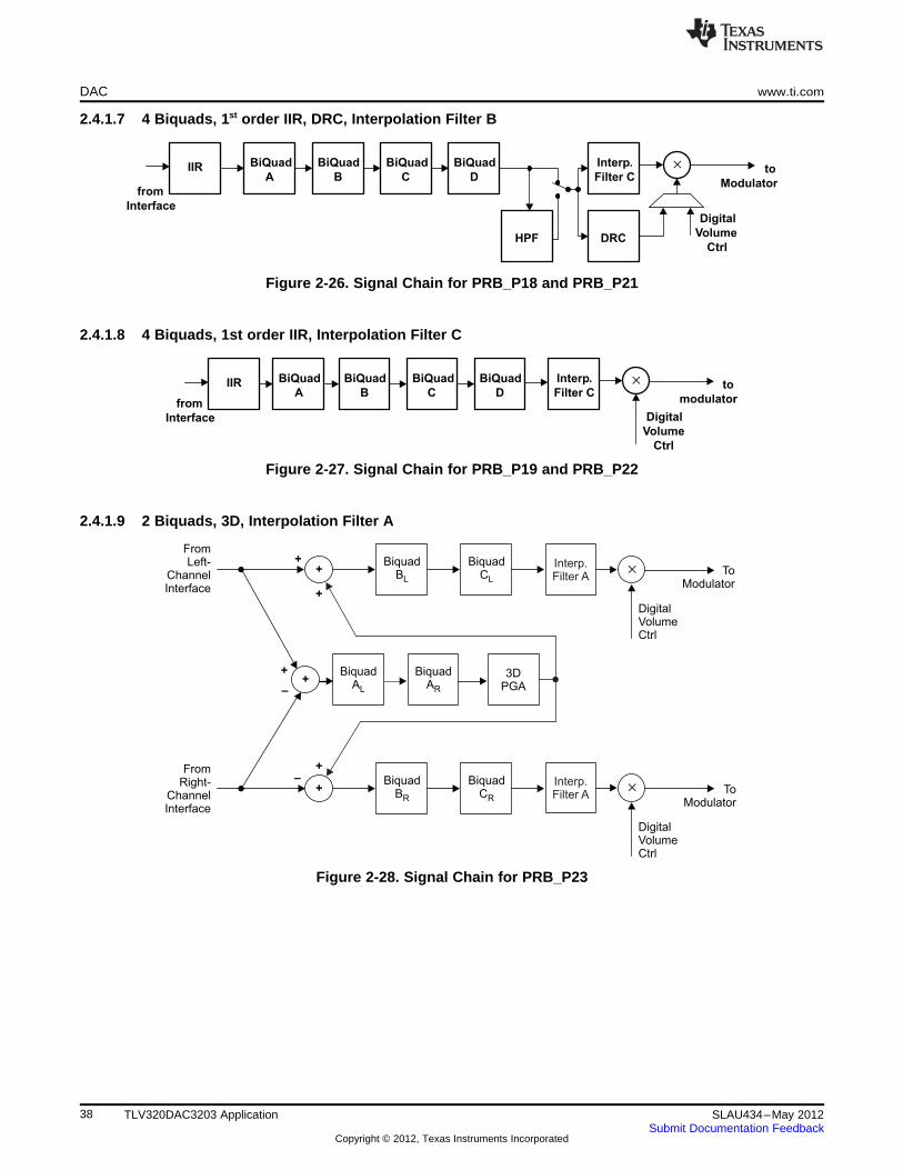
3DPGA
+
+
+
+
–
+
–
+
+
FromLeft-
ChannelInterface
ToModulator
DigitalVolumeCtrl
BiquadBL
ToModulator
´
´
BiquadCL
BiquadAL
BiquadAR
BiquadBR
BiquadCR
FromRight-
ChannelInterface
Interp.Filter A
Interp.Filter A
DigitalVolumeCtrl
Interp.
Filter C
BiQuad
D
BiQuad
C
BiQuad
B
BiQuad
AIIR to
modulator
Digital
Volume
Ctrl
from
Interface
´
Interp.
Filter C
DRCHPF
IIR to
Modulator
Digital
Volume
Ctrl
BiQuad
D
BiQuad
C
BiQuad
B
BiQuad
A
from
Interface
´
DAC www.ti.com
2.4.1.7 4 Biquads, 1st order IIR, DRC, Interpolation Filter B
Figure 2-26. Signal Chain for PRB_P18 and PRB_P21
2.4.1.8 4 Biquads, 1st order IIR, Interpolation Filter C
Figure 2-27. Signal Chain for PRB_P19 and PRB_P22
2.4.1.9 2 Biquads, 3D, Interpolation Filter A
Figure 2-28. Signal Chain for PRB_P23
38 TLV320DAC3203 Application SLAU434–May 2012Submit Documentation Feedback
Copyright © 2012, Texas Instruments Incorporated

DRCHPF
3DPGA
+
+
DRCHPF
+
+
–
+
–
+
+
FromLeft-
ChannelInterface
ToModulator
DigitalVolume
Ctrl
BiquadBL
´Biquad
CL
BiquadDL
BiquadAL
BiquadEL
BiquadFL
Interp.Filter A
Interp.Filter A
BiquadAR
FromRight-
ChannelInterface
BiquadBR
BiquadCR
BiquadDR
BiquadER
BiquadFR
ToModulator
DigitalVolumeCtrl
´
+
+
BeepGen.
Beep Volume Ctrl
Beep Volume Ctrl
´
´
IIRLeft
IIRRight
BiQuad
A L
Interp.
Filter A
DRCHPF
BiQuad
FL
BiQuad
EL
BiQuad
A R
IIR
Left
3D
PGA
+
+
Interp.
Filter A
DRCHPF
BiQuad
FR
BiQuad
ER
BiQuad
DR
BiQuad
CR
BiQuad
BR
IIR
Right+
+
-
+
-
+
+
from
Left
Channel
Interface
to
Modulator
to
Modulator
Digital
Volume
Ctrl
Digital
Volume
Ctrl
from
Right
Channel
Interface
BiQuad
BL
BiQuad
CL
BiQuad
DL´
´
www.ti.com DAC
2.4.1.10 5 Biquads, DRC, 3D, Interpolation Filter A
Figure 2-29. Signal Chain for PRB_P24
2.4.1.11 5 Biquads, DRC, 3D, Beep Generator, Interpolation Filter A
Figure 2-30. Signal Chain for PRB_P25
2.4.2 User Programmable Filters
Depending on the selected processing block, different types and orders of digital filtering are available. Upto 6 biquad sections are available for specific processing blocks.
39SLAU434–May 2012 TLV320DAC3203 ApplicationSubmit Documentation Feedback
Copyright © 2012, Texas Instruments Incorporated

2
2
1
1
23
2
2
1
10
zDzD*22
zNzN*2N)z(H
--
--
--
++
=
1
1
23
1
10
zD2
zNN)z(H
-
-
-
+
=
DAC www.ti.com
The coefficients of the available filters are arranged as sequentially-indexed coefficients in two banks. Ifadaptive filtering is chosen, the coefficient banks can be switched on-the-fly. For more details on adaptivefiltering please see Section 2.4.5.3.
The coefficients of these filters are each 24-bits wide, in two's-complement and occupy 3 consecutive 8-bitregisters in the register space. For default values please see the default values tables in the Register Mapsection.
2.4.2.1 1st-Order IIR Section
The IIR is of first-order and its transfer function is given by
(9)
The frequency response for the 1st order IIR Section with default coefficients is flat. Details on DACcoefficient default values are given in Section 5.19.
Table 2-14. DAC IIR Filter Coefficients
Filter Filter Coefficient ADC Coefficient Left Channel ADC Coefficient RightChannel
1st Order IIR N0 C65 (Page 46 / Registers C68 (Page 46 / Registers28,29,30) 40,41,42)
N1 C66 (Page 46 / Registers C69 (Page 46 / Registers32,33,34) 44,45,46)
D1 C67 (Page 46 / Registers V70 (Page 46 / Registers36,37,38) 48,49,50)
2.4.2.2 Biquad Section
The transfer function of each of the Biquad Filters is given by
(10)
The frequency response for each biquad section with default coefficients is flat at a gain of 0dB. Details onDAC coefficient default values are given in Section 5.19.
Table 2-15. DAC Biquad Filter Coefficients
Filter Coefficient Left DAC Channel Right DAC Channel
BIQUAD A N0 C1 (Page 44 / Registers 12,13,14) C33 (Page 45 / Registers 20,21,22)
N1 C2 (Page 44 / Registers 16,17,18) C34 (Page 45 / Registers 24,25,26)
N2 C3 (Page 44 / Registers 20,21,22) C35 (Page 45 / Registers 28,29,30)
D1 C4 (Page 44 / Registers 24,25,26) C36 (Page 45 / Registers 32,33,34)
D2 C5 (Page 44 / Registers 28,29,30) C37 (Page 45 / Registers 36,37,38)
BIQUAD B N0 C6 (Page 44 / Registers 32,33,34) C38 (Page 45 / Registers 40,41,42)
N1 C7 (Page 44 / Registers 36,37,38) C39 (Page 45 / Registers 44,45,46)
N2 C8 (Page 44 / Registers 40,41,42) C40 (Page 45 / Registers 48,49,50)
D1 C9 (Page 44 / Registers 44,45,46) C41 (Page 45 / Registers 52,53,54)
D2 C10 (Page 44 / Registers 48,49,50) C42 (Page 45 / Registers 56,57,58)
BIQUAD C N0 C11 (Page 44 / Registers 52,53,54) C43 (Page 45 / Registers 60,61,62)
N1 C12 (Page 44 / Registers 56,57,58) C44 (Page 45 / Registers 64,65,66)
N2 C13 (Page 44 / Registers 60,61,62) C45 (Page 45 / Registers 68,69,70)
D1 C14 (Page 44 / Registers 64,65,66) C46 (Page 45 / Registers 72,73,74)
D2 C15 (Page 44 / Registers 68,69,70) C47 (Page 45 / Registers 76,77,78)
BIQUAD D N0 C16 (Page 44 / Registers 72,73,74) C48 (Page 45 / Registers 80,81,82)
40 TLV320DAC3203 Application SLAU434–May 2012Submit Documentation Feedback
Copyright © 2012, Texas Instruments Incorporated

www.ti.com DAC
Table 2-15. DAC Biquad Filter Coefficients (continued)
Filter Coefficient Left DAC Channel Right DAC Channel
N1 C17 (Page 44 / Registers 76,77,78) C49 (Page 45 / Registers 84,85,86)
N2 C18 (Page 44 / Registers 80,81,82) C50 (Page 45 / Registers 88,89,90)
D1 C19 (Page 44 / Registers 84,85,86) C51 (Page 45 / Registers 92,93,94)
D2 C20 (Page 44 / Registers 88,89,90) C52 (Page 45 / Registers 96,97,98)
BIQUAD E N0 C21 (Page 44 / Registers 92,93,94) C53 (Page 45 / Registers 100,101,102)
N1 C22 (Page 44 / Registers 96,97,98) C54 (Page 45 / Registers 104,105,106)
N2 C23 (Page 44 / Registers 100,101,102) C55 (Page 45 / Registers 108,109,110)
D1 C24 (Page 44 / Registers 104,105,106) C56 (Page 45 / Registers 112,113,114)
D2 C25 (Page 44 / Registers 108,109,110) C57 (Page 45 / Registers 116,117,118)
BIQUAD F N0 C26 (Page 44 / Registers 112,113,114) C58 (Page 45 / Registers 120,121,122)
N1 C27 (Page 44 / Registers 116,117,118) C59 (Page 45 / Registers 124,125,126)
N2 C28 (Page 44 / Registers 120,121,122) C60 (Page 46 / Registers 8,9,10)
D1 C29 (Page 44 / Registers 124,125,126) C61 (Page 46 / Registers 12,13,14)
D2 C30 (Page 45 / Registers 8,9,10) C62 (Page 46 / Registers 16,17,18)
2.4.2.2.1 3D-PGA
The 3D-PGA attenuation block as used in the processing blocks PRB_P23, PRB_P24 and PRB_P25 canbe programmed in the range of -1.0 to +1.0. A value of -1.0 corresponds to 0x7FFFFF in DAC coefficientC32 (Page 45 / Register 16,17 and 18). A value of 1.0 corresponds to 0x800000 in coefficient C32.
41SLAU434–May 2012 TLV320DAC3203 ApplicationSubmit Documentation Feedback
Copyright © 2012, Texas Instruments Incorporated

0
–10
–20
–30
–40
–50
–60
–70
–80
–90
1 2 3 4 5 6 7
Frequency Normalized to fS
Magnitude
–dB
DAC Channel Response for Interpolation Filter A(Red line corresponds to –65 dB)
G016
DAC www.ti.com
2.4.3 Interpolation Filters
2.4.3.1 Interpolation Filter A
Filter A is designed for an Fs up to 48ksps with a flat passband of 0kHz–20kHz.
Table 2-16. DAC Interpolation Filter A, Specification
Parameter Condition Value (Typical) Units
Filter Gain Pass Band 0 … 0.45Fs ±0.015 dB
Filter Gain Stop Band 0.55Fs… 7.455Fs –65 dB
Filter Group Delay 21/Fs s
Figure 2-31. DAC Interpolation Filter A, Frequency Response
2.4.3.2 Interpolation Filter B
Filter B is specifically designed for an Fs of above 96ksps. Thus, the flat pass-band region easily coversthe required audio band of 0-20kHz.
Table 2-17. DAC Interpolation Filter B, Specification
Parameter Condition Value (Typical) Units
Filter Gain Pass Band 0 … 0.45Fs ±0.015 dB
Filter Gain Stop Band 0.55Fs… 3.45Fs –58 dB
Filter Group Delay 18/Fs s
42 TLV320DAC3203 Application SLAU434–May 2012Submit Documentation Feedback
Copyright © 2012, Texas Instruments Incorporated

DAC Channel Response for Interpolation Filter C(Red line corresponds to –43 dB)
0
–10
–20
–30
–40
–50
–60
–70
0.0 0.2 0.4 0.6 0.8 1.0 1.4
Frequency Normalized to fS
Magnitude
–dB
G018
1.2
0
–10
–20
–30
–40
–50
–60
–70
–80
0.5 1.0 1.5 2.0 2.5 3.0 3.5
Frequency Normalized to fS
Magnitude
–dB
G017
DAC Channel Response for Interpolation Filter B(Red line corresponds to –58 dB)
www.ti.com DAC
Figure 2-32. Channel Interpolation Filter B, Frequency Response
2.4.3.3 Interpolation Filter C
Filter C is specifically designed for the 192ksps mode. The pass band extends up to 0.40*Fs (correspondsto 80kHz), more than sufficient for audio applications.
Figure 2-33. DAC Interpolation Filter C, Frequency Response
Table 2-18. DAC Interpolation Filter C, Specification
Parameter Condition Value (Typical) Units
Filter Gain Pass Band 0 … 0.35Fs ±0.03 dB
Filter Gain Stop Band 0.60Fs… 1.4Fs –43 dB
Filter Group Delay 13/Fs s
43SLAU434–May 2012 TLV320DAC3203 ApplicationSubmit Documentation Feedback
Copyright © 2012, Texas Instruments Incorporated

1
1
23
1
10
LPF
zD2
zNN)z(H
-
-
-
+
=
1
1
23
1
10
HPF
zD2
zNN)z(H
-
-
-
+
=
DAC www.ti.com
2.4.4 DAC Gain Setting
2.4.4.1 Digital Volume Control
The TLV320DAC3203 signal processing blocks incorporate a digital volume control block that can controlthe volume of the playback signal from +24dB to –63.5dB in steps of 0.5dB. These can be controlled bywriting to Page 0, Register 65 and 66. The volume control of left and right channels by default can becontrolled independently, however by programming Page 0, Reg 64, Bits D1-D0), they can be madeinterdependent. The volume changes are soft-stepped in steps of 0.5dB to avoid audible artifacts duringgain change. The rate of soft-stepping can be controlled by programming Page 0, Reg 63, Bits D1-D0) toeither one step per frame (DAC_FS ) or one step per 2 frames. The soft-stepping feature can also beentirely disabled. During soft-stepping the value of the actual applied gain would differ from theprogrammed gain in register. The TLV320DAC3203 gives a feedback to the user in form of registerreadable flag to indicate that soft-stepping is currently in progress. The flags for left and right channels canbe read back by reading Page 0, Reg 38, Bits D4) and D(0) respectively. A value of 0 in these flagsindicates a soft-stepping operation in progress, and a value of 1 indicates that soft-stepping hascompleted. A soft-stepping operation comes into effect during a) power-up, when the volume control soft-steps from –63.5dB to programmed gain value b) volume change by user when DAC is powered up and c)power-down, when the volume control block soft-steps to –63.5dB before powering down the channel.
2.4.4.2 Dynamic Range Compression
Typical music signals are characterized by crest factors, the ratio of peak signal power to average signalpower, of 12dB or more. In order to avoid audible distortions due to clipping of peak signals, the gain ofthe DAC channel must be adjusted so as not to cause hard clipping of peak signals. As a result, duringnominal periods, the applied gain is low, causing the perception that the signal is not loud enough. Toovercome this problem, the DRC in the TLV320DAC3203 continuously monitors the output of the DACDigital Volume control to detect its power level w.r.t. 0dB FS. When the power level is low, it increases theinput signal gain to make it sound louder. At the same time, if a peaking signal is detected, itautonomously reduces the applied gain to avoid hard clipping. The resulting sound can be more pleasingto the ear as well as sounding louder during nominal periods.
The DRC functionality in the TLV320DAC3203 is implemented by a combination of Processing Blocks inthe DAC channel as described in Section 2.4.1.
The DRC can be disabled by writing into Page 0, Reg 68, Bits D6-D5).
The DRC typically works on the filtered version of the input signal. The input signals have no audioinformation at DC and extremely low frequencies; however they can significantly influence the energyestimation function in DRC. Also most of the information about signal energy is concentrated in the lowfrequency region of the input signal.
In order to estimate the energy of the input signal, the signal is first fed to the DRC high-pass filter andthen to the DRC low-pass filter. These filters are implemented as first-order IIR filters given by
(11)
(12)
The coefficients for these filters are 24-bits wide in two’s-complement and are user programmable throughregister write as given in Table 2-19, and coefficient default values are summarized in Section 5.19.
Table 2-19. DRC HPF and LPF Coefficients
Coefficient Location
HPF N0 C71 Page 46, Register 52 to 55
HPF N1 C72 Page 46, Register 56 to 59
HPF D1 C73 Page 46, Register 60 to 63
LPF N0 C74 Page 46, Register 64 to 67
LPF N1 C75 Page 46, Register 68 to 71
44 TLV320DAC3203 Application SLAU434–May 2012Submit Documentation Feedback
Copyright © 2012, Texas Instruments Incorporated

www.ti.com DAC
Table 2-19. DRC HPF and LPF Coefficients (continued)
Coefficient Location
LPF D1 C76 Page 46, Register 72 to 75
The default values of these coefficients implement a high-pass filter with a cut-off at 0.00166*DAC_FS,and a low-pass filter with a cutoff at 0.00033*DAC_FS.
The output of the DRC high-pass filter is fed to the Processing Block selected for the DAC Channel. Theabsolute value of the DRC-LPF filter is used for energy estimation within the DRC.
The gain in the DAC Digital Volume Control is controlled by Page 0, Register 65 and 66. When the DRC isenabled, the applied gain is a function of the Digital Volume Control register setting and the output of theDRC.
The DRC parameters are described in sections that follow.
2.4.4.2.1 DRC Threshold
The DRC Threshold represents the level of the DAC playback signal at which the gain compressionbecomes active. The output of the digital volume control in the DAC is compared with the set threshold.The threshold value is programmable by writing to register Page 0, Register 68, Bits D4-D2). TheThreshold value can be adjusted between –3dBFS to -24dBFS in steps of 3dB. Keeping the DRCThreshold value too high may not leave enough time for the DRC block to detect peaking signals, and cancause excessive distortion at the outputs. Keeping the DRC Threshold value too low can limit theperceived loudness of the output signal.
The recommended DRC-Threshold value is –24 dB.
When the output signal exceeds the set DRC Threshold, the interrupt flag bits at Page 0, Register 44, BitsD3-D2) are updated. These flag bits are 'sticky' in nature, and are reset only after they are read back bythe user. The non-sticky versions of the interrupt flags are also available at Page 0, Register 46, Bits D3-D2).
2.4.4.2.2 DRC Hysteresis
DRC Hysteresis is programmable by writing to Page 0, Register 68, Bits D1-D0). It can be programmed tovalues between 0dB and 3dB in steps of 1dB. It is a programmable window around the programmed DRCThreshold that must be exceeded for a disabled DRC to become enabled, or an enabled DRC to becomedisabled. For example, if the DRC Threshold is set to -12dBFS and DRC Hysteresis is set to 3dB, then ifthe gain compressions in the DRC is inactive, the output of the DAC Digital Volume Control must exceed–9dBFS before gain compression due to the DRC is activated. Similarly, when the gain compression inthe DRC is active, the output of the DAC Digital Volume Control needs to fall below -15dBFS for gaincompression in the DRC to be deactivated. The DRC Hysteresis feature prevents the rapid activation andde-activation of gain compression in the DRC in cases when the output of DAC Digital Volume Controlrapidly fluctuates in a narrow region around the programmed DRC Threshold. By programming the DRCHysteresis as 0dB, the hysteresis action is disabled.
Recommended Value of DRC Hysteresis is 3 dB.
2.4.4.2.3 DRC Hold
The DRC Hold is intended to slow the start of decay for a specified period of time in response to adecrease in energy level. To minimize audible artifacts, it is recommended to set the DRC Hold time to 0through programming Page 0, Register 69, Bits D6-D3) = 0000.
45SLAU434–May 2012 TLV320DAC3203 ApplicationSubmit Documentation Feedback
Copyright © 2012, Texas Instruments Incorporated
DAC www.ti.com
2.4.4.2.4 DRC Attack Rate
When the output of the DAC Digital Volume Control exceeds the programmed DRC Threshold, the gainapplied in the DAC Digital Volume Control is progressively reduced to avoid the signal from saturating thechannel. This process of reducing the applied gain is called Attack. To avoid audible artifacts, the gain isreduced slowly with a rate equaling the Attack Rate programmable via Page 0, Register 70, Bits D7-D4).Attack Rates can be programmed from 4dB gain change per 1/DAC_FS to 1.2207e-5dB gain change per1/DAC_FS.
Attack Rates should be programmed such that before the output of the DAC Digital Volume control canclip, the input signal should be sufficiently attenuated. High Attack Rates can cause audible artifacts, andtoo-slow Attack Rates may not be able to prevent the input signal from clipping.
The recommended DRC Attack Rate value is 1.9531e-4 dB per 1/DAC_FS.
2.4.4.2.5 DRC Decay Rate
When the DRC detects a reduction in output signal swing beyond the programmed DRC Threshold, theDRC enters a Decay state, where the applied gain in Digital Volume Control is gradually increased toprogrammed values. To avoid audible artifacts, the gain is slowly increased with a rate equal to the DecayRate programmed through Page 0, Register 70, Bits D3-D0). The Decay Rates can be programmed from1.5625e-3dB per 1/DAC_FS to 4.7683e-7dB per 1/DAC_FS. If the Decay Rates are programmed too high,then sudden gain changes can cause audible artifacts. However, if it is programmed too slow, then theoutput may be perceived as too low for a long time after the peak signal has passed.
The recommended Value of DRC Decay Rate is 2.4414e-5 dB per 1/DAC_FS.
2.4.4.2.6 Example Setup for DRC• PGA Gain = 12 dB
• Threshold = -24 dB
• Hysteresis = 3 dB
• Hold time = 0 ms
• Attack Rate = 1.9531e-4 dB per 1/DAC_FS
• Decay Rate = 2.4414e-5 dB per 1/DAC_FS
Script
w 30 00 00 #Go to Page 0w 30 41 18 #DAC => 12 db gain leftw 30 42 18 #DAC => 12 db gain rightw 30 44 7F #DAC => DRC Enabled for both channels, Threshold = -24 db, Hysteresis = 3 dBw 30 45 00 #DRC Hold = 0 ms, Rate of Changes of Gain = 0.5 dB/Fs'w 30 46 B6 #Attack Rate = 1.9531e-4 dB/Frame , DRC Decay Rate =2.4414e-5 dB/Framew 30 00 2E #Go to Page 46w 30 34 7F AB 00 00 80 55 00 00 7F 56 00 00 #DRC HPFw 30 40 00 11 00 00 00 11 00 00 7F DE 00 00 #DRC LPF
46 TLV320DAC3203 Application SLAU434–May 2012Submit Documentation Feedback
Copyright © 2012, Texas Instruments Incorporated

www.ti.com DAC
2.4.5 DAC Special Functions
2.4.5.1 Beep Generation
A special function has also been included in the processing block PRB_P25 for generating a digital sine-wave signal that is sent to the DAC. This is intended for generating key-click sounds for user feedback. Adefault value for the sine-wave frequency, sine burst length, and signal magnitude is kept in the ToneGenerator Registers Page 0 / Registers 71 through 79. The sine wave generator is very flexible, and iscompletely register programmable via 9 registers of 8 bits each to provide many different sounds.
Two registers are used for programming the 16-bit, two's-complement, sine-wave coefficient (Page 0 /Registers 76 and 77). Two other registers program the 16-bit, two's-complement, cosine-wave coefficient(Page 0 / Registers 78 and 79). This coefficient resolution allows virtually any frequency of sine wave inthe audio band to be generated up to DAC_FS/2.
Three registers are used to control the length of the sine burst waveform which are located on Page 0 /Registers 73, 74, and 75. The resolution (bit) in the registers of the sine burst length is one sample time,so this allows great control on the overall time of the sine burst waveform. This 24-bit length timersupports 16,777,215 sample times. (For example if DAC_FS is set at 48kHz, and the registers combinedvalue equals 96000d (01770h), then the sine burst would last exactly two seconds.)
Two registers are used to independently control the Left sine-wave volume and the Right sine-wavevolume. The 6-bit digital volume control allows level control of 0dB to –63dB in one dB steps. The left-channel volume is controlled by writing to Page 0 / Register 71, Bits D5-D0. The right-channel volume iscontrolled by Page 0 / Register 72, Bits D5-D0. A master volume control for the left and right channel ofthe beep generator can be set up using Page 0 / Register 72, Bits D7-D6. The default volume controlsetting is 0dB, the tone generator maximum-output level.
For playing back the sine wave, the DAC must be configured with regards to clock setup and routing. Thesine wave gets started by setting the Beep Generator Enable Bit (Page 1 / Register 71, Bit D7=1). Afterthe sine wave has played for its predefined time period this bit will automatically set back to 0. While thesine wave is playing, the parameters of the beep generator cannot be changed. To stop the sine wavewhile it is playing set the Beep Generator Enable Bit to 0.
2.4.5.2 Digital Auto Mute
The TLV320DAC3203 also incorporates a special feature, in which the DAC channel is auto-muted whena continuous stream of DC-input is detected. By default, this feature is disabled. It can be enabled bywriting a non-000 value into Page 0 / Register 64, Bits D6-D4. The non-zero value controls the duration ofcontinuous stream of DC-input before which the auto-mute feature takes effect. This feature is especiallyhelpful for eliminating high-frequency-noise power being delivered into the load even during silent periodsof speech or music.
2.4.5.3 Adaptive Filtering
When the DAC is running, the user-programmable filter coefficients are locked and cannot be accessedfor either read or write.
However the TLV320DAC3203 offers an adaptive filter mode as well. Setting Register Page 44,Reg 1, BitD2=1 will turn on double buffering of the coefficients. In this mode, filter coefficients can be updatedthrough the host, and activated without stopping and restarting the DAC. This enables advanced adaptivefiltering applications.
In the double-buffering scheme, all coefficients are stored in two buffers (Buffers A and B). When the DACis running and adaptive filtering mode is turned on, setting the control bit Page 44 / Register 1, Bit D0=1switches the coefficient buffers at the next start of a sampling period. This bit is set back to 0 after theswitch occurs. At the same time, the flag Page 44 / Reg 1, Bit D1) toggles.
The flag in Page 44 / Register 1, Bit D1) indicates which of the two buffers is actually in use.
Page 44 / Register 1, Bit D1=0: Buffer A is in use by the DAC engine, Bit D1=1: Buffer B is in use.
While the device is running, coefficient updates are always made to the buffer not in use by the DAC,regardless to which buffer the coefficients have been written.
47SLAU434–May 2012 TLV320DAC3203 ApplicationSubmit Documentation Feedback
Copyright © 2012, Texas Instruments Incorporated
DAC www.ti.com
DAC running Page 44 / Reg 1, Bits D1 Coefficient Buffer in use Writing to Will update
No 0 None C1, Buffer A C1, Buffer A
No 0 None C1, Buffer B C1, Buffer B
Yes 0 Buffer A C1, Buffer A C1, Buffer B
Yes 0 Buffer A C1, Buffer B C1, Buffer B
Yes 1 Buffer B C1, Buffer A C1, Buffer A
Yes 1 Buffer B C1, Buffer B C1, Buffer A
The user programmable coefficients C1 to C70 are defined on Pages 44, 45 and 46 for Buffer A andPages 62, 63 and 64 for Buffer B.
2.4.6 DAC Setup
The following paragraphs are intended to guide a user through the steps necessary to configure theTLV320DAC3203 DAC.
Step 1
The system clock source (master clock) and the targeted DAC sampling frequency must be identified.
Depending on the targeted performance the decimation filter type (A, B or C) and DOSR value can bedetermined.
Filter A should be used for 48kHz high-performance operation, DOSR must be a multiple of 8.Filter B should be used for up to 96kHz operations, DOSR must be a multiple of 4.Filter C should be used for up to 192kHz operations, DOSR must be a multiple of 2.
In all cases the DOSR is limited in its range by the following condition:
2.8MHz < DOSR * DAC_FS < 6.2MHz
Based on the identified filter type and the required signal processing capabilities, the appropriateprocessing block can be determined from the list of available processing blocks (PRB_P1 to PRB_P25).
Based on the available master clock, the chosen DOSR and the targeted sampling rate, the clock dividervalues NDAC and MDAC can be determined. If necessary, the internal PLL can add a large degree offlexibility.
In summary, Codec_Clkin (derived directly from the system clock source or from the internal PLL) dividedby MDAC, NDAC and DOSR must be equal to the DAC sampling rate DAC_FS. The codec_clkin clocksignal is shared with the ADC clock generation block.
CODEC_CLKIN = NDAC*MDAC*DOSR*DAC_FS
To a large degree, NDAC and MDAC can be chosen independently in the range of 1 to 128. In general,NDAC should be as large as possible as long as the following condition can still be met:
MDAC*DOSR/32 ≥ RC
RC is a function of the chosen processing block and is listed in Table 2-13.
The common-mode voltage setting of the device is determined by the available analog power supply. Thiscommon-mode (input common-mode) value is common across the ADC, DAC and analog bypass path.The output common-mode setting is determined by the available analog power supplies (AVdd and ) andthe desired output-signal swing.
At this point the following device specific parameters are known:
PRB_Px, DOSR, NDAC, MDAC, input and output common-mode values
If the PLL is used, the PLL parameters P, J, D and R are determined as well.
48 TLV320DAC3203 Application SLAU434–May 2012Submit Documentation Feedback
Copyright © 2012, Texas Instruments Incorporated

www.ti.com PowerTune
Step 2
Setting up the device via register programming:
The following list gives a sequence of items that must be executed in the time between powering thedevice up and reading data from the device:
Define starting point: Set register page to 0Initiate SW Reset
Program Clock Settings Program PLL clock dividers P,J,D,R (if PLL is necessary)Power up PLL (if PLL is necessary)Program and power up NDACProgram and power up MDACProgram OSR valueProgram I2S word length if required (e.g. 20bit)Program the processing block to be used
At this point, at the latest, the analog power supply must be applied to the device
Program Analog Blocks Set register Page to 1Disable coarse AVdd generationEnable Master Analog Power ControlProgram Common Mode voltageProgram Reference fast chargingProgram Headphone specific depop settings (in case of headphone driverused)Program routing of DAC output to the output amplifier (headphone)Unmute and set gain of output driverPower up output driver
Apply waiting time determined by the de-pop settings and the soft-stepping settings of the drivergain or poll Page 1 / Register 63
Power Up DAC Set register Page to 0Power up DAC ChannelsUnmute digital volume control
2.5 PowerTune
The TLV320DAC3203 features PowerTune, a mechanism to balance power-versus-performance trade-offs at the time of device configuration. The device can be tuned to minimize power dissipation, tomaximize performance, or to an operating point between the two extremes to best fit the application.
2.5.1 PowerTune Modes
2.5.1.1 DAC - Programming PTM_P1 to PTM_P4
On the playback side, the performance is determined by a combination of register settings and the audiodata word length applied. For the highest performance setting (PTM_P4), an audio-data word length of 20bits is required, while for the modes PTM_P1 to PTM_P3 a word length of 16 bits is sufficient.
PTM_P1 PTM_P2 PTM_P3 PTM_P4
Pg 1, Reg 3, D(4:2) 0x2 0x1 0x0 0x0
Pg 1, Reg 4, D(4:2) 0x2 0x1 0x0 0x0
Audio Data word length 16 bits 16 bits 16 bits 20 or more bits
Pg 0, Reg 27, D(5:4) 0x0 0x0 0x0 0x1, 0x2, 0x3
49SLAU434–May 2012 TLV320DAC3203 ApplicationSubmit Documentation Feedback
Copyright © 2012, Texas Instruments Incorporated

PowerTune www.ti.com
2.5.1.2 Processing Blocks
The choice of processing blocks, PRB_P1 to PRB_P25 for playback and PRB_R1 to PRB_R18 forrecording, also influences the power consumption. In fact, the numerous processing blocks have beenimplemented to offer a choice between power-optimization and configurations with more signal-processingresources.
50 TLV320DAC3203 Application SLAU434–May 2012Submit Documentation Feedback
Copyright © 2012, Texas Instruments Incorporated
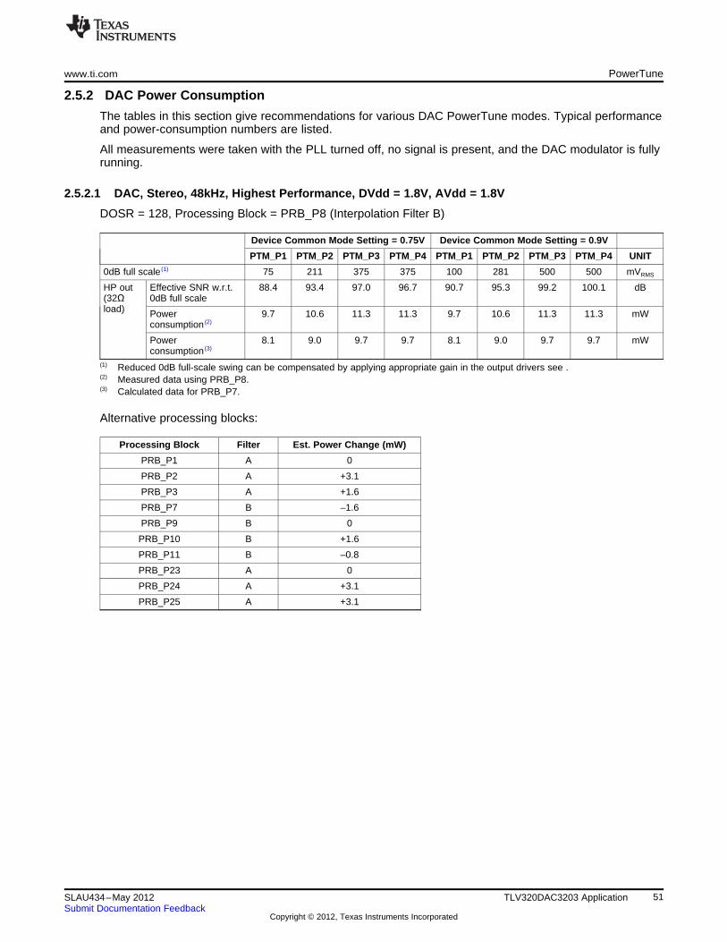
www.ti.com PowerTune
2.5.2 DAC Power Consumption
The tables in this section give recommendations for various DAC PowerTune modes. Typical performanceand power-consumption numbers are listed.
All measurements were taken with the PLL turned off, no signal is present, and the DAC modulator is fullyrunning.
2.5.2.1 DAC, Stereo, 48kHz, Highest Performance, DVdd = 1.8V, AVdd = 1.8V
DOSR = 128, Processing Block = PRB_P8 (Interpolation Filter B)
Device Common Mode Setting = 0.75V Device Common Mode Setting = 0.9V
PTM_P1 PTM_P2 PTM_P3 PTM_P4 PTM_P1 PTM_P2 PTM_P3 PTM_P4 UNIT
0dB full scale (1) 75 211 375 375 100 281 500 500 mVRMS
HP out Effective SNR w.r.t. 88.4 93.4 97.0 96.7 90.7 95.3 99.2 100.1 dB(32Ω 0dB full scaleload) Power 9.7 10.6 11.3 11.3 9.7 10.6 11.3 11.3 mW
consumption (2)
Power 8.1 9.0 9.7 9.7 8.1 9.0 9.7 9.7 mWconsumption (3)
(1) Reduced 0dB full-scale swing can be compensated by applying appropriate gain in the output drivers see .(2) Measured data using PRB_P8.(3) Calculated data for PRB_P7.
Alternative processing blocks:
Processing Block Filter Est. Power Change (mW)
PRB_P1 A 0
PRB_P2 A +3.1
PRB_P3 A +1.6
PRB_P7 B –1.6
PRB_P9 B 0
PRB_P10 B +1.6
PRB_P11 B –0.8
PRB_P23 A 0
PRB_P24 A +3.1
PRB_P25 A +3.1
51SLAU434–May 2012 TLV320DAC3203 ApplicationSubmit Documentation Feedback
Copyright © 2012, Texas Instruments Incorporated
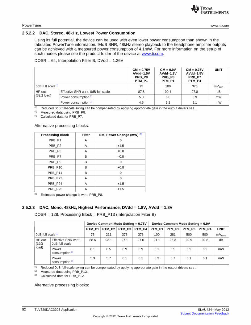
PowerTune www.ti.com
2.5.2.2 DAC, Stereo, 48kHz, Lowest Power Consumption
Using its full potential, the device can be used with even lower power consumption than shown in thetabulated PowerTune information. 94dB SNR, 48kHz stereo playback to the headphone amplifier outputscan be achieved with a measured power consumption of 4.1mW. For more information on the setup ofsuch modes please see the product folder of the device at www.ti.com.
DOSR = 64, Interpolation Filter B, DVdd = 1.26V
CM = 0.75V CM = 0.9V CM = 0.75V UNITAVdd=1.5V AVdd=1.8V AVdd=1.5V
PRB_P8 PRB_P8 PRB_P7PTM_P1 PTM_P1 PTM_P4
0dB full scale (1) 75 100 375 mVRMS
HP out Effective SNR w.r.t. 0dB full scale 87.8 90.4 97.8 dB(32Ω load) Power consumption (2) 5.3 6.0 5.9 mW
Power consumption (3) 4.5 5.2 5.1 mW(1) Reduced 0dB full-scale swing can be compensated by applying appropriate gain in the output drivers see .(2) Measured data using PRB_P8.(3) Calculated data for PRB_P7.
Alternative processing blocks:
Processing Block Filter Est. Power Change (mW) (1)
PRB_P1 A 0
PRB_P2 A +1.5
PRB_P3 A +0.8
PRB_P7 B –0.8
PRB_P9 B 0
PRB_P10 B +0.8
PRB_P11 B 0
PRB_P23 A 0
PRB_P24 A +1.5
PRB_P25 A +1.5(1) Estimated power change is w.r.t. PRB_P8.
2.5.2.3 DAC, Mono, 48kHz, Highest Performance, DVdd = 1.8V, AVdd = 1.8V
DOSR = 128, Processing Block = PRB_P13 (Interpolation Filter B)
Device Common Mode Setting = 0.75V Device Common Mode Setting = 0.9V
PTM_P1 PTM_P2 PTM_P3 PTM_P4 PTM_P1 PTM_P2 PTM_P3 PTM_P4 UNIT
0dB full scale (1) 75 211 375 375 100 281 500 500 mVRMS
HP out Effective SNR w.r.t. 88.6 93.1 97.1 97.0 91.1 95.3 99.9 99.8 dB(32Ω 0dB full scaleload) Power 6.1 6.5 6.9 6.9 6.1 6.5 6.9 6.9 mW
consumption (2)
Power 5.3 5.7 6.1 6.1 5.3 5.7 6.1 6.1 mWconsumption (3)
(1) Reduced 0dB full-scale swing can be compensated by applying appropriate gain in the output drivers see .(2) Measured data using PRB_P13.(3) Calculated data for PRB_P12.
Alternative processing blocks:
52 TLV320DAC3203 Application SLAU434–May 2012Submit Documentation Feedback
Copyright © 2012, Texas Instruments Incorporated

www.ti.com PowerTune
Processing Block Filter Est. Power Change(mW)
PRB_P4 A 0
PRB_P5 A +1.6
PRB_P6 A +1.6
PRB_P12 B –0.8
PRB_P14 B 0
PRB_P15 B +1.6
PRB_P16 B 0
2.5.2.4 DAC, Mono, 48kHz, Lowest Power Consumption
DOSR = 64, Processing Block = PRB_P13 (Interpolation Filter B), PowerTune Mode = PTM_P1, DVdd =1.26V
CM = 0.75V CM = 0.9V UNITAVdd=1.5V AVdd=1.8V
0dB full scale (1) 75 100 mVRMS
HP out Effective SNR w.r.t. 0dB full scale 88.7 91.5 dB(32Ω load) Power consumption (2) 3.3 3.7 mW
Power consumption (3) 2.9 3.3 mW(1) Reduced 0dB full-scale swing can be compensated by applying appropriate gain in the output drivers see .(2) Measured data using PRB_P13.(3) Calculated data for PRB_P12.
Alternative processing blocks:
Processing Block Filter Est. Power Change (mW)
PRB_P4 A 0
PRB_P5 A +0.8
PRB_P6 A +0.8
PRB_P12 B –0.4
PRB_P14 B 0
PRB_P15 B +0.8
PRB_P16 B 0
2.5.2.5 DAC, Stereo, 8kHz, Highest Performance, DVdd = 1.8V, AVdd = 1.8V
DOSR = 768, Processing Block = PRB_P7 (Interpolation Filter B)
Device Common Mode Setting = 0.75V Device Common Mode Setting = 0.9V
PTM_P1 PTM_P2 PTM_P3 PTM_P4 PTM_P1 PTM_P2 PTM_P3 PTM_P4 UNIT
0dB full scale 75 211 375 375 100 281 500 500 mVRMS
HP out Effective SNR w.r.t. 88.3 93.3 97.7 98.0 90.5 95.3 99.2 99.7 dB(32Ω 0dB full scale (1)
load) Power consumption 6.8 7.8 8.5 8.5 6.8 7.8 8.5 8.5 mW(1) Reduced 0dB full-scale swing can be compensated by applying appropriate gain in the output drivers see .
Alternative processing blocks:
Processing Block Filter Est. Power Change (mW)
PRB_P1 A +0.3
PRB_P2 A +0.8
PRB_P3 A +0.5
53SLAU434–May 2012 TLV320DAC3203 ApplicationSubmit Documentation Feedback
Copyright © 2012, Texas Instruments Incorporated

PowerTune www.ti.com
Processing Block Filter Est. Power Change (mW)
PRB_P8 B +0.3
PRB_P9 B +0.3
PRB_P10 B +0.5
PRB_P11 B +0.3
PRB_P23 A +0.3
PRB_P24 A +0.8
PRB_P25 A +0.8
2.5.2.6 DAC, Stereo, 8kHz, Lowest Power Consumption
DOSR = 384, Processing Block = PRB_P7 (Interpolation Filter B), PowerTune Mode = PTM_P1, DVdd =1.26V
CM = 0.75V CM = 0.9V UNITAVdd=1.5V AVdd=1.8V
0dB full scale (1) 75 100 mVRMS
HP out Effective SNR w.r.t. 0dB full scale 88.4 90.7 dB(32Ω load) Power consumption 3.9 4.6 mW
(1) Reduced 0dB full-scale swing can be compensated by applying appropriate gain in the output drivers see .
Alternative processing blocks:
Processing Block Filter Est. Power Change (mW)
PRB_P1 A +0.1
PRB_P2 A +0.4
PRB_P3 A +0.3
PRB_P8 B +0.1
PRB_P9 B +0.1
PRB_P10 B +0.3
PRB_P11 B +0.1
PRB_P23 A +0.1
PRB_P24 A +0.4
PRB_P25 A +0.4
2.5.2.7 DAC, Mono, 8kHz, Highest Performance, DVdd = 1.8V, AVdd = 1.8V
DOSR = 768, Processing Block = PRB_P4 (Interpolation Filter A)
Device Common Mode Setting = 0.75V Device Common Mode Setting = 0.9V
PTM_P1 PTM_P2 PTM_P3 PTM_P4 PTM_P1 PTM_P2 PTM_P3 PTM_P4 UNIT
0dB full scale (1) 75 211 375 375 100 281 500 500 mVRMS
HP out Effective SNR w.r.t. 89.1 92.6 97.0 96.8 91.0 95.0 99.4 100.5 dB(32Ω 0dB full scaleload) Power consumption 4.7 5.2 5.5 5.5 4.7 5.2 5.5 5.5 mW
(1) Reduced 0dB full-scale swing can be compensated by applying appropriate gain in the output drivers see .
Alternative processing blocks:
Processing Block Filter Est. Power Change (mW)
PRB_P5 A +0.3
PRB_P6 A +0.3
PRB_P12 B –0.1
54 TLV320DAC3203 Application SLAU434–May 2012Submit Documentation Feedback
Copyright © 2012, Texas Instruments Incorporated

www.ti.com PowerTune
Processing Block Filter Est. Power Change (mW)
PRB_P13 B 0
PRB_P14 B 0
PRB_P15 B +0.3
PRB_P16 B 0
2.5.2.8 DAC, Mono, 8kHz, Lowest Power Consumption
DOSR = 384, Processing Block = PRB_P4 (Interpolation Filter A), PowerTune Mode = PTM_P1, DVdd =1.26V
CM = 0.75V CM = 0.9V UNITAVdd=1.5V AVdd=1.8V
0dB full scale (1) 75 100 mVRMS
HP out Effective SNR w.r.t. 88.4 91.1 dB(32Ω load) 0dB full scale
Power consumption 2.5 2.9 mW(1) Reduced 0dB full-scale swing can be compensated by applying appropriate gain in the output drivers see .
Alternative processing blocks:
Processing Block Filter Est. Power Change (mW)
PRB_P5 A +0.1
PRB_P6 A +0.1
PRB_P12 B –0.1
PRB_P13 B 0
PRB_P14 B 0
PRB_P15 B +0.1
PRB_P16 B 0
2.5.2.9 DAC, Stereo, 192kHz, DVdd = 1.8V, AVdd = 1.8V
DOSR = 32, Processing Block = PRB_P17 (Interpolation Filter C)
Device Common Mode Setting = 0.75V Device Common Mode Setting = 0.9V
PTM_P1 PTM_P2 PTM_P3 PTM_P4 PTM_P1 PTM_P2 PTM_P3 PTM_P4 UNIT
0dB full scale (1) 75 211 375 375 100 281 500 500 mVRMS
HP out Effective SNR w.r.t. 88.3 92.1 96.4 97.2 90.7 94.6 99.3 99.7 dB(32Ω 0dB full scaleload) Power consumption 11.3 12.3 13.0 13.1 11.3 12.3 13.0 13.1 mW
(1) Reduced 0dB full-scale swing can be compensated by applying appropriate gain in the output drivers see .
Alternative processing blocks:
Processing Block Filter Est. Power Change (mW)
PRB_P18 C +9.3
PRB_P19 C +3.1
55SLAU434–May 2012 TLV320DAC3203 ApplicationSubmit Documentation Feedback
Copyright © 2012, Texas Instruments Incorporated
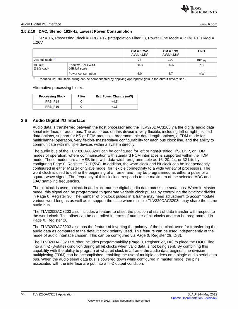
Audio Digital I/O Interface www.ti.com
2.5.2.10 DAC, Stereo, 192kHz, Lowest Power Consumption
DOSR = 16, Processing Block = PRB_P17 (Interpolation Filter C), PowerTune Mode = PTM_P1, DVdd =1.26V
CM = 0.75V CM = 0.9V UNITAVdd=1.5V AVdd=1.8V
0dB full scale (1) 75 100 mVRMS
HP out Effective SNR w.r.t. 88.3 90.6 dB(32Ω load) 0dB full scale
Power consumption 6.0 6.7 mW(1) Reduced 0dB full-scale swing can be compensated by applying appropriate gain in the output drivers see .
Alternative processing blocks:
Processing Block Filter Est. Power Change (mW)
PRB_P18 C +4.5
PRB_P19 C +1.5
2.6 Audio Digital I/O Interface
Audio data is transferred between the host processor and the TLV320DAC3203 via the digital audio dataserial interface, or audio bus. The audio bus on this device is very flexible, including left or right-justifieddata options, support for I2S or PCM protocols, programmable data length options, a TDM mode formultichannel operation, very flexible master/slave configurability for each bus clock line, and the ability tocommunicate with multiple devices within a system directly.
The audio bus of the TLV320DAC3203 can be configured for left or right-justified, I2S, DSP, or TDMmodes of operation, where communication with standard PCM interfaces is supported within the TDMmode. These modes are all MSB-first, with data width programmable as 16, 20, 24, or 32 bits byconfiguring Page 0, Register 27, D(5:4). In addition, the word clock and bit clock can be independentlyconfigured in either Master or Slave mode, for flexible connectivity to a wide variety of processors. Theword clock is used to define the beginning of a frame, and may be programmed as either a pulse or asquare-wave signal. The frequency of this clock corresponds to the maximum of the selected ADC andDAC sampling frequencies.
The bit clock is used to clock in and clock out the digital audio data across the serial bus. When in Mastermode, this signal can be programmed to generate variable clock pulses by controlling the bit-clock dividerin Page 0, Register 30. The number of bit-clock pulses in a frame may need adjustment to accommodatevarious word-lengths as well as to support the case when multiple TLV320DAC3203s may share the sameaudio bus.
The TLV320DAC3203 also includes a feature to offset the position of start of data transfer with respect tothe word-clock. This offset can be controlled in terms of number of bit-clocks and can be programmed inPage 0, Register 28.
The TLV320DAC3203 also has the feature of inverting the polarity of the bit-clock used for transferring theaudio data as compared to the default clock polarity used. This feature can be used independently of themode of audio interface chosen. This can be configured via Page 0, Register 29, D(3).
The TLV320DAC3203 further includes programmability (Page 0, Register 27, D0) to place the DOUT lineinto a hi-Z (3-state) condition during all bit clocks when valid data is not being sent. By combining thiscapability with the ability to program at what bit clock in a frame the audio data begins, time-divisionmultiplexing (TDM) can be accomplished, enabling the use of multiple codecs on a single audio serial databus. When the audio serial data bus is powered down while configured in master mode, the pinsassociated with the interface are put into a hi-Z output condition.
56 TLV320DAC3203 Application SLAU434–May 2012Submit Documentation Feedback
Copyright © 2012, Texas Instruments Incorporated
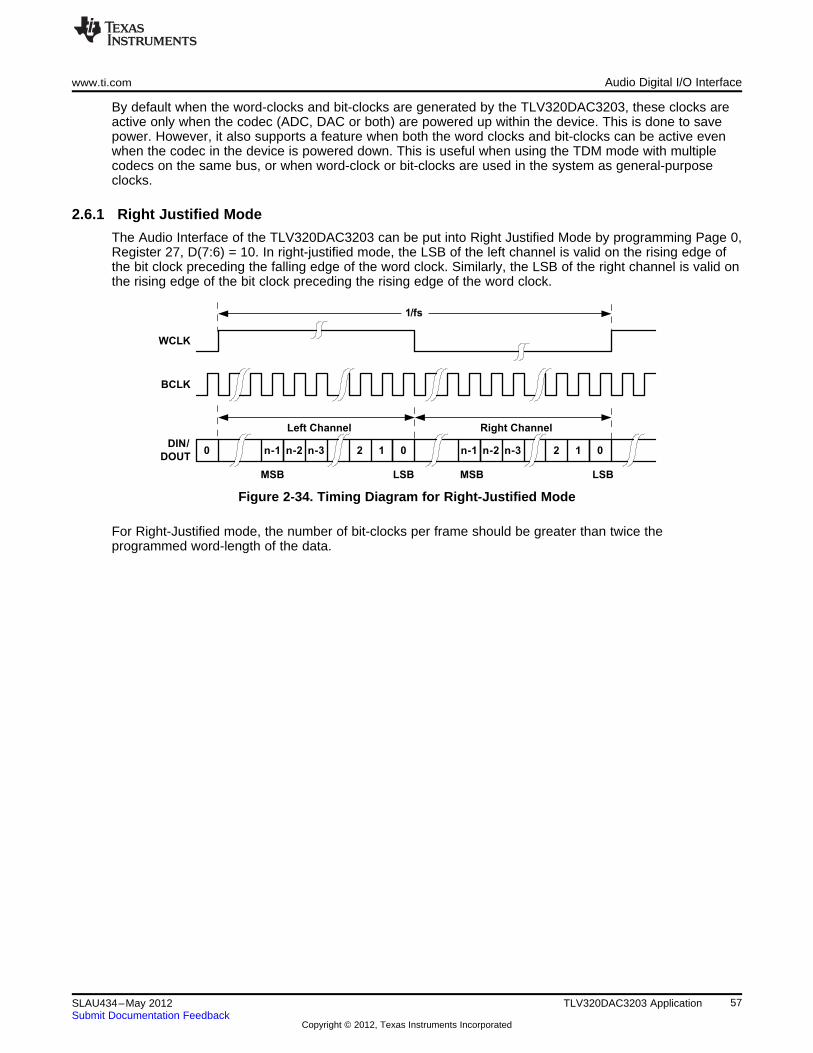
BCLK
WCLK
DIN/
DOUTn-1 n-2 1 00 n-1 n-2 1 0
LSBMSB
Left Channel Right Channel
n-3 2 2n-3
LSBMSB
1/fs
www.ti.com Audio Digital I/O Interface
By default when the word-clocks and bit-clocks are generated by the TLV320DAC3203, these clocks areactive only when the codec (ADC, DAC or both) are powered up within the device. This is done to savepower. However, it also supports a feature when both the word clocks and bit-clocks can be active evenwhen the codec in the device is powered down. This is useful when using the TDM mode with multiplecodecs on the same bus, or when word-clock or bit-clocks are used in the system as general-purposeclocks.
2.6.1 Right Justified Mode
The Audio Interface of the TLV320DAC3203 can be put into Right Justified Mode by programming Page 0,Register 27, D(7:6) = 10. In right-justified mode, the LSB of the left channel is valid on the rising edge ofthe bit clock preceding the falling edge of the word clock. Similarly, the LSB of the right channel is valid onthe rising edge of the bit clock preceding the rising edge of the word clock.
Figure 2-34. Timing Diagram for Right-Justified Mode
For Right-Justified mode, the number of bit-clocks per frame should be greater than twice theprogrammed word-length of the data.
57SLAU434–May 2012 TLV320DAC3203 ApplicationSubmit Documentation Feedback
Copyright © 2012, Texas Instruments Incorporated

LD(n) LD(n+1)
WORDCLOCK
BITCLOCK
DATA 3N-1
N-2
N-3
2 1 03N-1
N-2
N-3
2 1 03N-1
N-2
N-3
RD(n)
LEFT CHANNEL RIGHT CHANNEL
LD(n) = n'th sample of left channel data RD(n) = n'th sample of right channel data
LD(n) LD(n+1)
WORDCLOCK
BITCLOCK
DATA -1
-2
-3
2 1 03 -1
-2
-3
2 1 03 -1
-2
N N N N N N N N N-3
RD(n)
LEFT CHANNEL RIGHT CHANNEL
LD(n) = n'th sample of left channel data RD(n) = n'th sample of right channel data
LD(n) LD(n+1)
WORDCLOCK
BITCLOCK
DATA -1
-2
-3
2 1 03 -1
-2
-3
2 1 03 -1
-2
N N N N N N N N N-3
RD(n)
LEFT CHANNEL RIGHT CHANNEL
LD(n) = n'th sample of left channel data RD(n) = n'th sample of right channel data
Audio Digital I/O Interface www.ti.com
2.6.2 Left Justified Mode
The Audio Interface of the TLV320DAC3203 can be put into Left Justified Mode by programming Page 0,Register 27, D(7:6) = 11. In left-justified mode, the MSB of the right channel is valid on the rising edge ofthe bit clock following the falling edge of the word clock. Similarly the MSB of the left channel is valid onthe rising edge of the bit clock following the rising edge of the word clock.
Figure 2-35. Timing Diagram for Left-Justified Mode
Figure 2-36. Timing Diagram for Left-Justified Mode with Offset=1
Figure 2-37. Timing Diagram for Left-Justified Mode with Offset=0 and inverted bit clock
For Left-Justified mode, the number of bit-clocks per frame should be greater than twice the programmedword-length of the data. Also, the programmed offset value should be less than the number of bit-clocksper frame by at least the programmed word-length of the data.
58 TLV320DAC3203 Application SLAU434–May 2012Submit Documentation Feedback
Copyright © 2012, Texas Instruments Incorporated
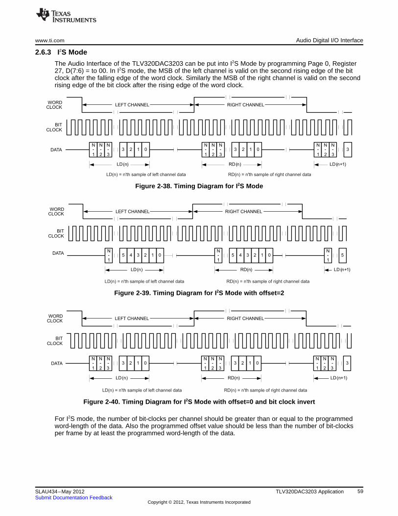
LD(n) LD(n+1)
WORDCLOCK
BITCLOCK
DATA -1
-2
-3
2 1 03 -1
-2
-3
2 1 03 -1
-2
N N N N N N N N N-3
3
RD(n)
LEFT CHANNEL RIGHT CHANNEL
LD(n) = n'th sample of left channel data RD(n) = n'th sample of right channel data
LD(n) LD (n+1)
WORDCLOCK
BITCLOCK
DATA -1
4 3 25 1 0 -1
4 3 25 1 0N N N
-1
5
RD(n)
LEFT CHANNEL RIGHT CHANNEL
LD(n) = n'th sample of left channel data RD(n) = n'th sample of right channel data
LD(n) LD(n+1)
WORDCLOCK
BITCLOCK
DATA -1
-2
-3
2 1 03 -1
-2
-3
2 1 03 -1
-2
N N N N N N N N N-3
3
RD(n)
LEFT CHANNEL RIGHT CHANNEL
LD(n) = n'th sample of left channel data RD(n) = n'th sample of right channel data
www.ti.com Audio Digital I/O Interface
2.6.3 I2S Mode
The Audio Interface of the TLV320DAC3203 can be put into I2S Mode by programming Page 0, Register27, D(7:6) = to 00. In I2S mode, the MSB of the left channel is valid on the second rising edge of the bitclock after the falling edge of the word clock. Similarly the MSB of the right channel is valid on the secondrising edge of the bit clock after the rising edge of the word clock.
Figure 2-38. Timing Diagram for I2S Mode
Figure 2-39. Timing Diagram for I2S Mode with offset=2
Figure 2-40. Timing Diagram for I2S Mode with offset=0 and bit clock invert
For I2S mode, the number of bit-clocks per channel should be greater than or equal to the programmedword-length of the data. Also the programmed offset value should be less than the number of bit-clocksper frame by at least the programmed word-length of the data.
59SLAU434–May 2012 TLV320DAC3203 ApplicationSubmit Documentation Feedback
Copyright © 2012, Texas Instruments Incorporated

LD(n) LD(n+1)
BIT
CLOCK
DATA
N-
1
N-
2
N-
3
2 1 03N-
1
N-
2
N-
3
03 2 1N-
1
N-
2
N-
3
3
RD(n)
WORD
CLOCKLEFT CHANNEL RIGHT CHANNEL
LD(n) LD(n+1)
BITCLOCK
DATA -1
-2
-3
2 1 03 -1
-2
-3
03 2 1 -1
-2
N N N N N N N N N-3
RD(n)
WORDCLOCK
LEFT CHANNEL RIGHT CHANNEL
LD(n) = n'th sample of left channel data RD(n) = n'th sample of right channel data
LD(n) LD(n+1)
BITCLOCK
DATA -1
-2
-3
2 1 03 -1
-2
-3
03 2 1 -1
-2
N N N N N N N N N-3
3
RD(n)
WORDCLOCK
LEFT CHANNEL RIGHT CHANNEL
LD(n) = n'th sample of left channel data RD(n) = n'th sample of right channel data
Audio Digital I/O Interface www.ti.com
2.6.4 DSP Mode
The Audio Interface of the TLV320DAC3203 can be put into DSP Mode by programming Page 0, Register27, D(7:6) = 01. In DSP mode, the rising edge of the word clock starts the data transfer with the leftchannel data first and immediately followed by the right channel data. Each data bit is valid on the fallingedge of the bit clock.
Figure 2-41. Timing Diagram for DSP Mode
Figure 2-42. Timing Diagram for DSP Mode with offset = 1
Figure 2-43. Timing Diagram for DSP Mode with offset = 0 and bit clock inverted
For DSP mode, the number of bit-clocks per frame should be greater than twice the programmed word-length of the data. Also the programmed offset value should be less than the number of bit-clocks perframe by at least the programmed word-length of the data.
60 TLV320DAC3203 Application SLAU434–May 2012Submit Documentation Feedback
Copyright © 2012, Texas Instruments Incorporated

BCLK
WCLK
DOUT
DOUT_int
S_DIN
BCLK
DIN
WCLK
DIN
DOUT
Primary
Audio
Processor
S_WCLK
DAC_FS
ADC_FS
S_BCLK
BCLK_OUT
BCLK
S_BCLK
WCLK
S_WCLK
DIN
S_DIN
WCLK
ADC_WCLK
Audio
Digital
Serial
Interface
BCLK_INT
DAC_WCLK_INT
ADC_WCLK_INT
DIN_INT
GPIO
SCLK
MISO
S_BCLK
DOUT
BCLK
BCLK_OUT
GPIO
SCLK
MISO
S_WCLK
DOUT
WCLK
DAC_FS
ADC_FS
GPIO
SCLK
S_DIN
DOUT_int
DIN
MISO
(S_DOUT)
Clock
Generation
BCLK_OUT
DAC_FS
ADC_FSWCLK
DIN
DOUT
Secondary
Audio
Processor
BCLK
GPIO
SCLK
MISO
ADC_FS
ADC_WCLK
BCLK2
WCLK2
www.ti.com Audio Digital I/O Interface
2.6.5 Secondary I2S
The audio serial interface on the TLV320DAC3203 has an extensive IO control to allow communicationwith two independent processors for audio data. Each processor can communicate with the device one ata time. This feature is enabled by register programming of the various pin selections.
Figure 2-44. Audio Serial Interface Multiplexing
The secondary audio interface uses multifunction pins. For an overview on multifunction pins please seeSection 2.1.3. Figure 2-44 illustrates possible audio interface routing. The multifunction pins SCLK andMISO are only available in I2C communication mode.
This multiplexing capability allows the TLV320DAC3203 to communicate with two separate devices withindependent I2S/PCM busses, one at a time.
61SLAU434–May 2012 TLV320DAC3203 ApplicationSubmit Documentation Feedback
Copyright © 2012, Texas Instruments Incorporated
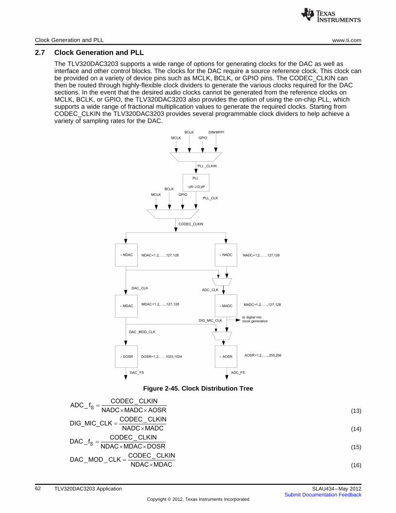
MDACNDAC
CLKIN_CODECCLK_MOD_DAC
´
=
DOSRMDACNDAC
CLKIN_CODEC
´´
fS_DAC =
MADCNADC
CLKIN_CODECDIG_MIC_CLK
´
=
AOSRMADCNADC
CLKIN_CODECfS_ADC
´´
=
PLL
×(R×J·D)/P
¸ NADC
PLL _CLKIN
CODEC_CLKIN
ADC _CLKDAC_CLK
DIG_MIC_CLK
DAC _MOD_CLK
NADC=1,2,…..,127,128
MADC=1,2,…..,127,128
AOSR=1,2,…..,255,256
NDAC=1,2,…..,127,128
MDAC=1,2,…..,127,128
DOSR=1,2,…..,1023,1024
MCLK
BCLK
GPIO
DIN/MFP1
MCLK
BCLK
GPIOPLL_CLK
¸ NDAC
¸ MADC¸ MDAC
¸ AOSR¸ DOSR
ADC_FSDAC_FS
to digital micclock generation
Clock Generation and PLL www.ti.com
2.7 Clock Generation and PLL
The TLV320DAC3203 supports a wide range of options for generating clocks for the DAC as well asinterface and other control blocks. The clocks for the DAC require a source reference clock. This clock canbe provided on a variety of device pins such as MCLK, BCLK, or GPIO pins. The CODEC_CLKIN canthen be routed through highly-flexible clock dividers to generate the various clocks required for the DACsections. In the event that the desired audio clocks cannot be generated from the reference clocks onMCLK, BCLK, or GPIO, the TLV320DAC3203 also provides the option of using the on-chip PLL, whichsupports a wide range of fractional multiplication values to generate the required clocks. Starting fromCODEC_CLKIN the TLV320DAC3203 provides several programmable clock dividers to help achieve avariety of sampling rates for the DAC.
Figure 2-45. Clock Distribution Tree
(13)
(14)
(15)
(16)
62 TLV320DAC3203 Application SLAU434–May 2012Submit Documentation Feedback
Copyright © 2012, Texas Instruments Incorporated
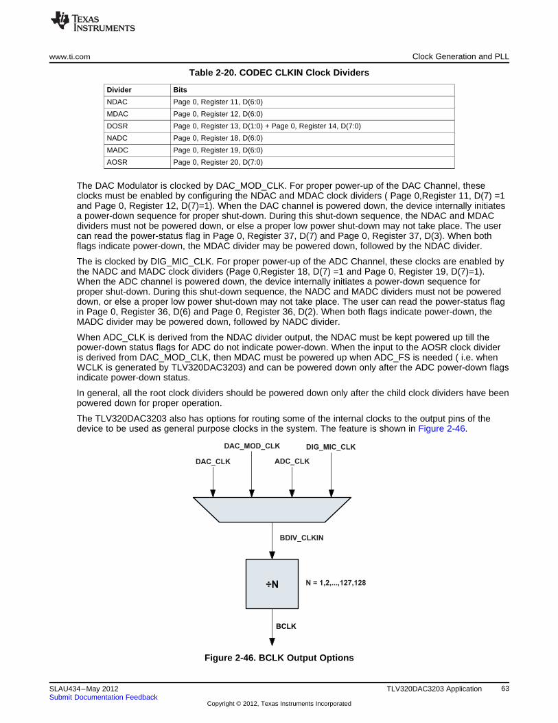
÷N
BCLK
DAC_CLK
DIG_MIC_CLKDAC_MOD_CLK
ADC_CLK
BDIV_CLKIN
N = 1,2,...,127,128
www.ti.com Clock Generation and PLL
Table 2-20. CODEC CLKIN Clock Dividers
Divider Bits
NDAC Page 0, Register 11, D(6:0)
MDAC Page 0, Register 12, D(6:0)
DOSR Page 0, Register 13, D(1:0) + Page 0, Register 14, D(7:0)
NADC Page 0, Register 18, D(6:0)
MADC Page 0, Register 19, D(6:0)
AOSR Page 0, Register 20, D(7:0)
The DAC Modulator is clocked by DAC_MOD_CLK. For proper power-up of the DAC Channel, theseclocks must be enabled by configuring the NDAC and MDAC clock dividers ( Page 0,Register 11, D(7) =1and Page 0, Register 12, D(7)=1). When the DAC channel is powered down, the device internally initiatesa power-down sequence for proper shut-down. During this shut-down sequence, the NDAC and MDACdividers must not be powered down, or else a proper low power shut-down may not take place. The usercan read the power-status flag in Page 0, Register 37, D(7) and Page 0, Register 37, D(3). When bothflags indicate power-down, the MDAC divider may be powered down, followed by the NDAC divider.
The is clocked by DIG_MIC_CLK. For proper power-up of the ADC Channel, these clocks are enabled bythe NADC and MADC clock dividers (Page 0,Register 18, D(7) =1 and Page 0, Register 19, D(7)=1).When the ADC channel is powered down, the device internally initiates a power-down sequence forproper shut-down. During this shut-down sequence, the NADC and MADC dividers must not be powereddown, or else a proper low power shut-down may not take place. The user can read the power-status flagin Page 0, Register 36, D(6) and Page 0, Register 36, D(2). When both flags indicate power-down, theMADC divider may be powered down, followed by NADC divider.
When ADC_CLK is derived from the NDAC divider output, the NDAC must be kept powered up till thepower-down status flags for ADC do not indicate power-down. When the input to the AOSR clock divideris derived from DAC_MOD_CLK, then MDAC must be powered up when ADC_FS is needed ( i.e. whenWCLK is generated by TLV320DAC3203) and can be powered down only after the ADC power-down flagsindicate power-down status.
In general, all the root clock dividers should be powered down only after the child clock dividers have beenpowered down for proper operation.
The TLV320DAC3203 also has options for routing some of the internal clocks to the output pins of thedevice to be used as general purpose clocks in the system. The feature is shown in Figure 2-46.
Figure 2-46. BCLK Output Options
63SLAU434–May 2012 TLV320DAC3203 ApplicationSubmit Documentation Feedback
Copyright © 2012, Texas Instruments Incorporated

÷M
CLKOUT
CDIV_CLKIN
MCLK BCLK DIN
GPIO MISO DOUT
PLL_CLK
DAC_CLK ADC_CLK
DAC_MOD_CLK DIG_MIC_CLK
M = 1,2,...,127,128
Clock Generation and PLL www.ti.com
In the mode when TLV320DAC3203 is configured to drive the BCLK pin (Page 0, Register 27, D3=’1’) itcan be driven as divided value of BDIV_CLKIN. The division value can be programmed in Page 0,Register 30, D(6:0) from 1 to 128. The BDIV_CLKIN can itself be configured to be one of DAC_CLK,DAC_MOD_CLK, ADC_CLK or DIG_MIC_CLK by configuring the BDIV_CLKIN mux in Page 0, Register29, D(1:0). Additionally a general purpose clock can be driven out on either GPIO, DOUT or MISO pin.This clock can be a divided down version of CDIV_CLKIN. The value of this clock divider can beprogrammed from 1 to 128 by writing to Page 0, Register 26, D(6:0). The CDIV_CLKIN can itself beprogrammed as one of the clocks among the list shown in Figure 2-47. This can be controlled byprogramming the mux in Page 0, Register 25, D(2:0).
Figure 2-47. General Purpose Clock Output Options
Table 2-21. Maximum TLV320DAC3203 Clock Frequencies
DVdd ≥ 1.26V DVdd ≥ 1.65V
CODEC_CLKIN 50MHz 137MHz when NDAC is even, NADC is even112MHz when NDAC is even, NADC is odd110MHz when NDAC is odd, NADC is even110MHz when NDAC is odd, NADC is odd
ADC_CLK 25MHz 55.296MHz
DIG_MIC_CLK 6.758MHz 6.758MHz
ADC_FS 0.192MHz 0.192MHz
DAC_CLK 25MHz 55.296MHz
DAC_MOD_CLK 6.758MHz 6.758MHz4.2MHz when Class-D Mode Headphone
is used
DAC_FS 0.192MHz 0.192MHz
BDIV_CLKIN 25MHz 55.296MHz
CDIV_CLKIN 50MHz 112MHz when M is odd137MHz when M is even
64 TLV320DAC3203 Application SLAU434–May 2012Submit Documentation Feedback
Copyright © 2012, Texas Instruments Incorporated

MHz20P
CLKIN_PLLMHz10 ££
MHz20P
CLKIN_PLLkHz512 ££
PLL _ CLKIN R J.DPLL _ CLK
P
´ ´
=
www.ti.com Clock Generation and PLL
2.7.1 PLL
The TLV320DAC3203 has an on-chip PLL to generate the clock frequency for the audio ADC, DAC, andDigital Signal Processing blocks. The programmability of the PLL allows operation from a wide variety ofclocks that may be available in the system.
The PLL input supports clocks varying from 512kHz to 20MHz and is register programmable to enablegeneration of required sampling rates with fine resolution. The PLL can be turned on by writing to Page 0,Register 5, D(7). When the PLL is enabled, the PLL output clock PLL_CLK is given by the followingequation:
(17)
R = 1, 2, 3, 4
J = 1, 2, 3, 4,… 63, and D = 0, 1, 2, 3, 4, … 9999
P = 1, 2, 3, 4, … 8
R, J, D, and P are register programmable.
The PLL can be programmed via Page 0, Registers 5-8. The PLL can be turned on via Page 0, Register5, D(7). The variable P can be programmed via Page 0, Register 5, D(6:4). The default register value for Pis 1, and for J is 4. The variable R can be programmed via Page 0, Register 5, D(3:0). The default registervalue for R is 1. The variable J can be programmed via Page 0, Register 6, D(5:0). The variable D is 12-bits, programmed into two registers. The MSB portion can be programmed via Page 0, Register 7, D(5:0),and the LSB portion is programmed via Page 0, Register 8, D(7:0). The default register value for D is 0.
When the PLL is enabled the following conditions must be satisfied
• When the PLL is enabled and D = 0, the following conditions must be satisfied for PLL_CLKIN:
(18)
• When the PLL is enabled and D ≠ 0, the following conditions must be satisfied for PLL_CLKIN:
(19)
In the TLV320DAC3203 the PLL_CLK supports a wide range of output clock, based on register settingsand power-supply conditions.
Table 2-22. PLL_CLK Frequency Range
AVdd PLL Mode Min PLL_CLK Max PLL_CLKPage 0, Reg 4, D6 frequency (MHz) frequency (MHz)
≥1.5V 0 80 103
1 95 110
≥1.65V 0 80 118
1 92 123
≥1.80V 0 80 132
1 92 137
The PLL can be powered up independently from the ADC and DAC blocks, and can also be used as ageneral purpose PLL by routing its output to the GPIO output. After powering up the PLL, PLL_CLK isavailable typically after 10ms. The PLL output frequency is controlled by J.D and R dividers
PLL Divider Bits
J Page 0, Register 6, D(5:0)
D Page 0, Register 7, D(5:0) && Page 0, Register 8, D(7:0)
R Page 0, Register 5, D(3:0)
65SLAU434–May 2012 TLV320DAC3203 ApplicationSubmit Documentation Feedback
Copyright © 2012, Texas Instruments Incorporated

Control Interfaces www.ti.com
The D-divider value is 14-bits wide and is controlled by 2 registers. For proper update of the D-dividervalue, Page 0, Register 7 must be programmed first followed immediately by Page 0, Register 8. Unlessthe write to Page 0, Register 8 is completed, the new value of D will not take effect.
The clocks for codec and various signal processing blocks, CODEC_CLKIN can be generated from MCLKinput, BCLK input, GPIO input or PLL_CLK (Page 0/Register 4/D(1:0) ).
If the CODEC_CLKIN is derived from the PLL, then the PLL must be powered up first and powered downlast.
Table 2-23 lists several example cases of typical MCLK rates and how to program the PLL to achieve asample rate Fs of either 44.1kHz or 48kHz.
Table 2-23. PLL Example Configurations
Fs = 44.1kHz
MCLK (MHz) PLLP PLLR PLLJ PLLD MADC NADC AOSR MDAC NDAC DOSR
2.8224 1 3 10 0 3 5 128 3 5 128
5.6448 1 3 5 0 3 5 128 3 5 128
12 1 1 7 560 3 5 128 3 5 128
13 1 2 4 2336 13 3 64 4 6 104
16 1 1 5 2920 3 5 128 3 5 128
19.2 1 1 4 4100 3 5 128 3 5 128
48 4 1 7 560 3 5 128 3 5 128
Fs = 48kHz
2.048 1 3 14 0 2 7 128 7 2 128
3.072 1 4 7 0 2 7 128 7 2 128
4.096 1 3 7 0 2 7 128 7 2 128
6.144 1 2 7 0 2 7 128 7 2 128
8.192 1 4 3 0 2 8 128 4 4 128
12 1 1 7 1680 2 7 128 7 2 128
16 1 1 5 3760 2 7 128 7 2 128
19.2 1 1 4 4800 2 7 128 7 2 128
48 4 1 7 1680 2 7 128 7 2 128
2.8 Control Interfaces
The TLV320DAC3203 control interface supports SPI or I2C communication protocols, with the protocolselectable using the SPI_SELECT pin. For SPI, SPI_SELECT should be tied high; for I2C, SPI_SELECTshould be tied low. It is not recommended to change the state of SPI_SELECT during device operation.
2.8.1 I2C Control Mode
The TLV320DAC3203 supports the I2C control protocol, and will respond to the I2C address of 0011000.I2C is a two-wire, open-drain interface supporting multiple devices and masters on a single bus. Deviceson the I2C bus only drive the bus lines LOW by connecting them to ground; they never drive the bus linesHIGH. Instead, the bus wires are pulled HIGH by pullup resistors, so the bus wires are HIGH when nodevice is driving them LOW. This way, two devices cannot conflict; if two devices drive the bussimultaneously, there is no driver contention.
Communication on the I2C bus always takes place between two devices, one acting as the master and theother acting as the slave. Both masters and slaves can read and write, but slaves can only do so underthe direction of the master. Some I2C devices can act as masters or slaves, but the TLV320DAC3203 canonly act as a slave device.
An I2C bus consists of two lines, SDA and SCL. SDA carries data, and the SCL signal provides the clock.All data is transmitted across the I2C bus in groups of eight bits. To send a bit on the I2C bus, the SDA lineis driven to the appropriate level while SCL is LOW (a LOW on SDA indicates the bit is zero, while a HIGHindicates the bit is one).
66 TLV320DAC3203 Application SLAU434–May 2012Submit Documentation Feedback
Copyright © 2012, Texas Instruments Incorporated
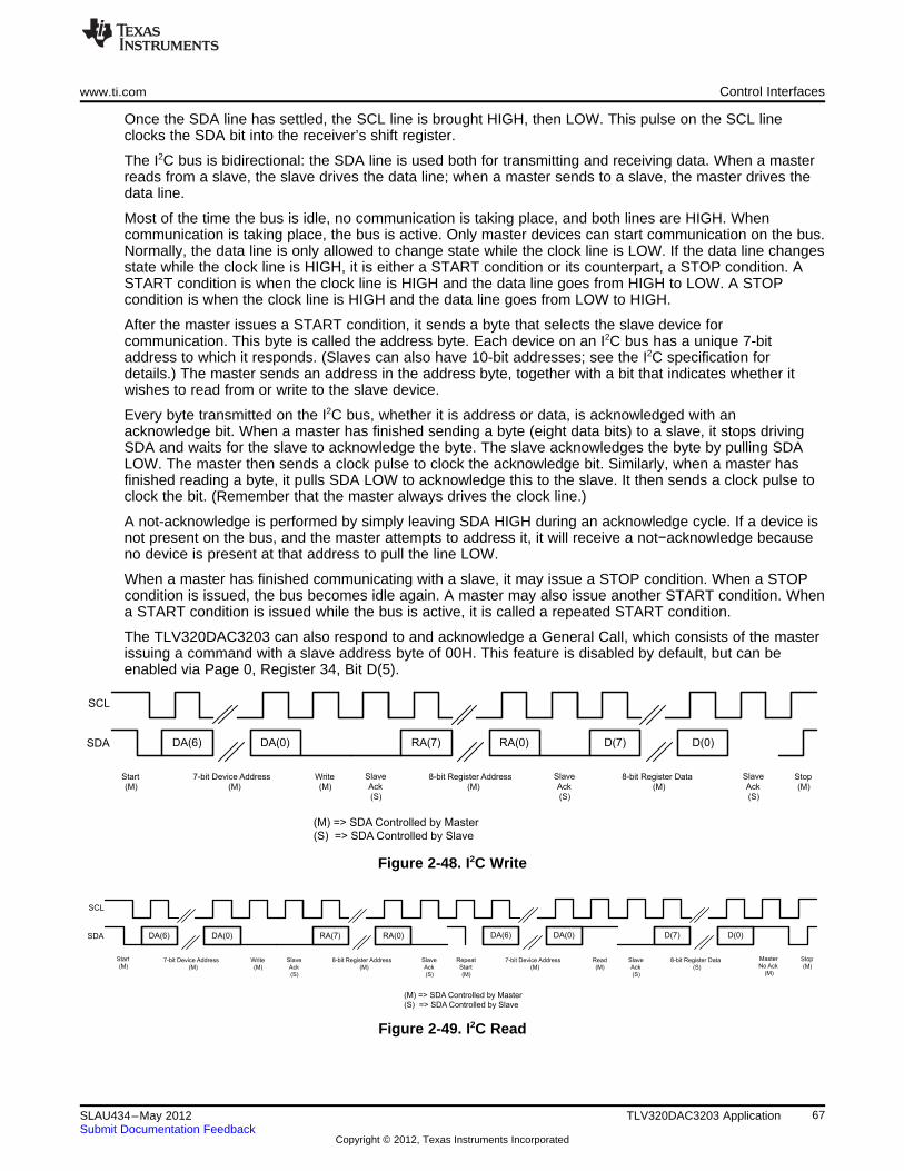
Start
(M)7-bit Device Address
(M)
Write
(M)
Slave
Ack
(S)
8-bit Register Address
(M)
Slave
Ack
(S)
SDA
SCL
7-bit Device Address
(M)
Read
(M)
Slave
Ack
(S)
DA(6) DA(0) RA(7) RA(0) DA(6) DA(0) D(7) D(0)
8-bit Register Data
(S)
Stop
(M)
Master
No Ack
(M)
Repeat
Start
(M)
(M) => SDA Controlled by Master
(S) => SDA Controlled by Slave
DA(6) DA(0) RA(7) RA(0) D(7) D(0)
Start
(M)
7-bit Device Address
(M)
Write
(M)
Slave
Ack
(S)
8-bit Register Address
(M)
Slave
Ack
(S)
8-bit Register Data
(M)
Stop
(M)
Slave
Ack
(S)
SDA
SCL
(M) => SDA Controlled by Master
(S) => SDA Controlled by Slave
www.ti.com Control Interfaces
Once the SDA line has settled, the SCL line is brought HIGH, then LOW. This pulse on the SCL lineclocks the SDA bit into the receiver’s shift register.
The I2C bus is bidirectional: the SDA line is used both for transmitting and receiving data. When a masterreads from a slave, the slave drives the data line; when a master sends to a slave, the master drives thedata line.
Most of the time the bus is idle, no communication is taking place, and both lines are HIGH. Whencommunication is taking place, the bus is active. Only master devices can start communication on the bus.Normally, the data line is only allowed to change state while the clock line is LOW. If the data line changesstate while the clock line is HIGH, it is either a START condition or its counterpart, a STOP condition. ASTART condition is when the clock line is HIGH and the data line goes from HIGH to LOW. A STOPcondition is when the clock line is HIGH and the data line goes from LOW to HIGH.
After the master issues a START condition, it sends a byte that selects the slave device forcommunication. This byte is called the address byte. Each device on an I2C bus has a unique 7-bitaddress to which it responds. (Slaves can also have 10-bit addresses; see the I2C specification fordetails.) The master sends an address in the address byte, together with a bit that indicates whether itwishes to read from or write to the slave device.
Every byte transmitted on the I2C bus, whether it is address or data, is acknowledged with anacknowledge bit. When a master has finished sending a byte (eight data bits) to a slave, it stops drivingSDA and waits for the slave to acknowledge the byte. The slave acknowledges the byte by pulling SDALOW. The master then sends a clock pulse to clock the acknowledge bit. Similarly, when a master hasfinished reading a byte, it pulls SDA LOW to acknowledge this to the slave. It then sends a clock pulse toclock the bit. (Remember that the master always drives the clock line.)
A not-acknowledge is performed by simply leaving SDA HIGH during an acknowledge cycle. If a device isnot present on the bus, and the master attempts to address it, it will receive a not−acknowledge becauseno device is present at that address to pull the line LOW.
When a master has finished communicating with a slave, it may issue a STOP condition. When a STOPcondition is issued, the bus becomes idle again. A master may also issue another START condition. Whena START condition is issued while the bus is active, it is called a repeated START condition.
The TLV320DAC3203 can also respond to and acknowledge a General Call, which consists of the masterissuing a command with a slave address byte of 00H. This feature is disabled by default, but can beenabled via Page 0, Register 34, Bit D(5).
Figure 2-48. I2C Write
Figure 2-49. I2C Read
67SLAU434–May 2012 TLV320DAC3203 ApplicationSubmit Documentation Feedback
Copyright © 2012, Texas Instruments Incorporated
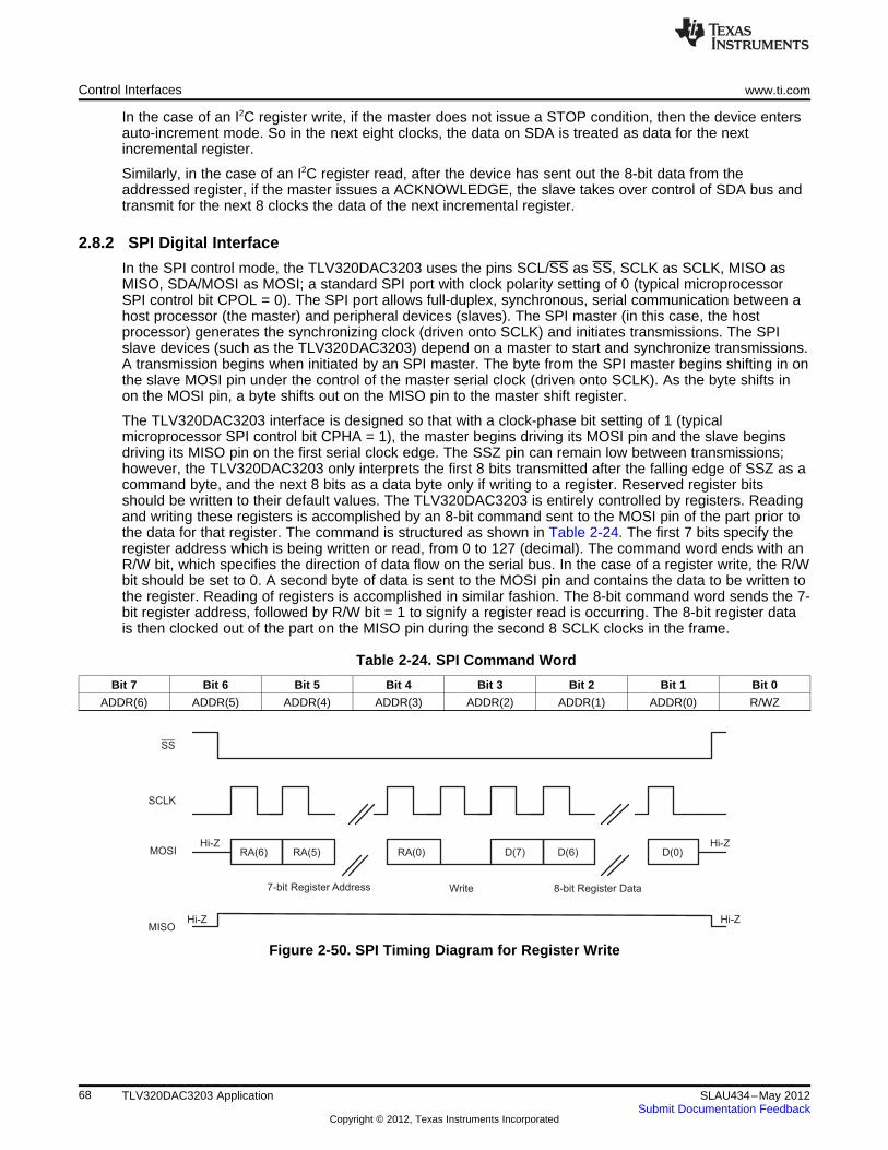
RA(6) RA(5) RA(0) D(7) D(6) D(0)
7-bit Register Address Write 8-bit Register Data
SS
SCLK
MOSI
MISO
Hi-Z Hi-Z
Hi-Z Hi-Z
Control Interfaces www.ti.com
In the case of an I2C register write, if the master does not issue a STOP condition, then the device entersauto-increment mode. So in the next eight clocks, the data on SDA is treated as data for the nextincremental register.
Similarly, in the case of an I2C register read, after the device has sent out the 8-bit data from theaddressed register, if the master issues a ACKNOWLEDGE, the slave takes over control of SDA bus andtransmit for the next 8 clocks the data of the next incremental register.
2.8.2 SPI Digital Interface
In the SPI control mode, the TLV320DAC3203 uses the pins SCL/SS as SS, SCLK as SCLK, MISO asMISO, SDA/MOSI as MOSI; a standard SPI port with clock polarity setting of 0 (typical microprocessorSPI control bit CPOL = 0). The SPI port allows full-duplex, synchronous, serial communication between ahost processor (the master) and peripheral devices (slaves). The SPI master (in this case, the hostprocessor) generates the synchronizing clock (driven onto SCLK) and initiates transmissions. The SPIslave devices (such as the TLV320DAC3203) depend on a master to start and synchronize transmissions.A transmission begins when initiated by an SPI master. The byte from the SPI master begins shifting in onthe slave MOSI pin under the control of the master serial clock (driven onto SCLK). As the byte shifts inon the MOSI pin, a byte shifts out on the MISO pin to the master shift register.
The TLV320DAC3203 interface is designed so that with a clock-phase bit setting of 1 (typicalmicroprocessor SPI control bit CPHA = 1), the master begins driving its MOSI pin and the slave beginsdriving its MISO pin on the first serial clock edge. The SSZ pin can remain low between transmissions;however, the TLV320DAC3203 only interprets the first 8 bits transmitted after the falling edge of SSZ as acommand byte, and the next 8 bits as a data byte only if writing to a register. Reserved register bitsshould be written to their default values. The TLV320DAC3203 is entirely controlled by registers. Readingand writing these registers is accomplished by an 8-bit command sent to the MOSI pin of the part prior tothe data for that register. The command is structured as shown in Table 2-24. The first 7 bits specify theregister address which is being written or read, from 0 to 127 (decimal). The command word ends with anR/W bit, which specifies the direction of data flow on the serial bus. In the case of a register write, the R/Wbit should be set to 0. A second byte of data is sent to the MOSI pin and contains the data to be written tothe register. Reading of registers is accomplished in similar fashion. The 8-bit command word sends the 7-bit register address, followed by R/W bit = 1 to signify a register read is occurring. The 8-bit register datais then clocked out of the part on the MISO pin during the second 8 SCLK clocks in the frame.
Table 2-24. SPI Command Word
Bit 7 Bit 6 Bit 5 Bit 4 Bit 3 Bit 2 Bit 1 Bit 0
ADDR(6) ADDR(5) ADDR(4) ADDR(3) ADDR(2) ADDR(1) ADDR(0) R/WZ
Figure 2-50. SPI Timing Diagram for Register Write
68 TLV320DAC3203 Application SLAU434–May 2012Submit Documentation Feedback
Copyright © 2012, Texas Instruments Incorporated
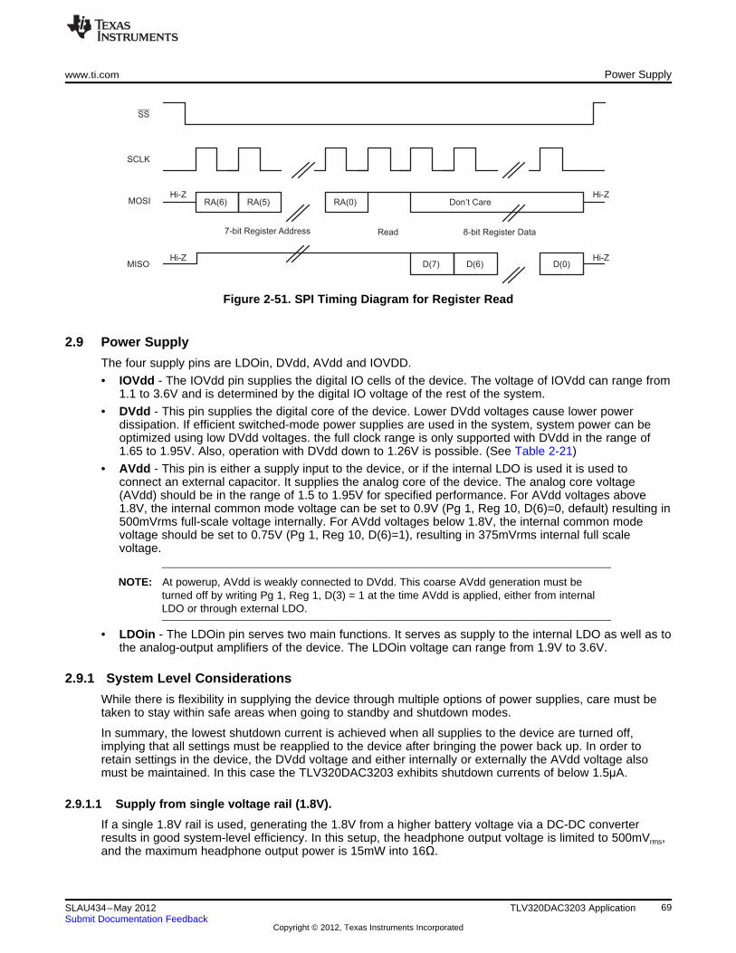
RA(6) RA(5) RA(0) Don’t Care
7-bit Register Address Read 8-bit Register Data
SS
SCLK
MOSI
MISO
Hi-Z Hi-Z
D(7) D(6) D(0)Hi-Z Hi-Z
www.ti.com Power Supply
Figure 2-51. SPI Timing Diagram for Register Read
2.9 Power Supply
The four supply pins are LDOin, DVdd, AVdd and IOVDD.
• IOVdd - The IOVdd pin supplies the digital IO cells of the device. The voltage of IOVdd can range from1.1 to 3.6V and is determined by the digital IO voltage of the rest of the system.
• DVdd - This pin supplies the digital core of the device. Lower DVdd voltages cause lower powerdissipation. If efficient switched-mode power supplies are used in the system, system power can beoptimized using low DVdd voltages. the full clock range is only supported with DVdd in the range of1.65 to 1.95V. Also, operation with DVdd down to 1.26V is possible. (See Table 2-21)
• AVdd - This pin is either a supply input to the device, or if the internal LDO is used it is used toconnect an external capacitor. It supplies the analog core of the device. The analog core voltage(AVdd) should be in the range of 1.5 to 1.95V for specified performance. For AVdd voltages above1.8V, the internal common mode voltage can be set to 0.9V (Pg 1, Reg 10, D(6)=0, default) resulting in500mVrms full-scale voltage internally. For AVdd voltages below 1.8V, the internal common modevoltage should be set to 0.75V (Pg 1, Reg 10, D(6)=1), resulting in 375mVrms internal full scalevoltage.
NOTE: At powerup, AVdd is weakly connected to DVdd. This coarse AVdd generation must beturned off by writing Pg 1, Reg 1, D(3) = 1 at the time AVdd is applied, either from internalLDO or through external LDO.
• LDOin - The LDOin pin serves two main functions. It serves as supply to the internal LDO as well as tothe analog-output amplifiers of the device. The LDOin voltage can range from 1.9V to 3.6V.
2.9.1 System Level Considerations
While there is flexibility in supplying the device through multiple options of power supplies, care must betaken to stay within safe areas when going to standby and shutdown modes.
In summary, the lowest shutdown current is achieved when all supplies to the device are turned off,implying that all settings must be reapplied to the device after bringing the power back up. In order toretain settings in the device, the DVdd voltage and either internally or externally the AVdd voltage alsomust be maintained. In this case the TLV320DAC3203 exhibits shutdown currents of below 1.5μA.
2.9.1.1 Supply from single voltage rail (1.8V).
If a single 1.8V rail is used, generating the 1.8V from a higher battery voltage via a DC-DC converterresults in good system-level efficiency. In this setup, the headphone output voltage is limited to 500mVrms,and the maximum headphone output power is 15mW into 16Ω.
69SLAU434–May 2012 TLV320DAC3203 ApplicationSubmit Documentation Feedback
Copyright © 2012, Texas Instruments Incorporated

Reference Voltage www.ti.com
The 1.8V rail connected to the DVdd pincan also be connected to the AVdd pin. This connection will makethe device function, but the achievable performance is a function of the voltage ripple typically found onDC-DC converter outputs. To achieve specified performance, an external low-input-voltage 1.6V LDOmust be connected between the 1.8V rail and the AVdd input.
During operation, the AVdd LDO is deactivated via control register Page 1 / Register 2, D(0)=0. In thiscase the LDOin pin should be connected to DVdd.
2.9.1.1.1 Standby Mode (1.8V operation)
To put the device in standby mode, both external voltages (AVdd and DVdd) and the reference blockinside the TLV320DAC3203 must stay on (Page 1 / Register 123, D(2:0) = 101), all other blocks should bepowered down. This results in standby current of approximately 100μA from the AVdd supply.
In standby mode the device responds very quickly to playback requests.
2.9.1.1.2 Sleep Mode (1.8V operation)
In this mode, all settings and memory content of the device is retained. To put the device into sleep mode,the external DVdd must remain powered up, the external AVdd LDO must be powered down, the crudeAVdd generation must be turned on (Pg 1, Reg 1, D(3)=0) and the analog blocks must be powered down(Pg 1, Reg 2, D(3)=1). The device's sleep mode power consumption in this case is < 1.5μA
2.9.1.1.3 Shutdown Mode
To shut down the device, the external supplies can be turned off completely. If the 1.8V rail cannot beturned off, the crude AVdd generation must be turned on (Pg 1, Reg 1, D(3)=0) and the analog blocksmust be powered down (Pg 1, Reg 2, D(3)=1). This results in a device shutdown current < 1.5μA.
2.9.1.2 Other Supply Options
There are other options to power the device. Apply the following rules:
• During normal operation all supply pins must be connected to a supply (via internal LDO or external)
• Whenever the LDOin supply is present,
– DVdd supply must be present as well
– If AVdd supply is not present, then the crude internal AVdd generation must be turned on (Pg 1,Reg 1, D(3)=0)
• Whenever the DVdd supply is on, and either AVdd or LDOin or both supplies are off, the analog blocksmust be powered down (Pg 1, Reg 2, D(3)=1)
2.10 Reference Voltage
All data converters require a DC reference voltage. The TLV320DAC3203 achieves its low-noiseperformance by internally generating a low-noise reference voltage. This reference voltage is generatedusing a band-gap circuit with a good PSRR performance. This reference voltage must be filteredexternally using a minimum 1μF capacitor connected from the REF pin to analog ground (AVss).
This reference block is powered down when all analog blocks inside the device are powered down. In thiscondition, the REF pin is 3-stated. On powerup of any analog block, the reference block is also poweredup and the REF pin settles to its steady-state voltage after the settling time (a function of the de-couplingcapacitor on the REF pin). This time is approximately equal to 1 second when using a 1μF decouplingcapacitor. In the event that a faster power-up is required, either the reference block can be kept poweredup (even when no other analog block is powered up) by programming Page 1, Register 123, D(2) = 1.However, in this case, an additional 125μA of current from AVdd is consumed. Additionally, to achieve afaster powerup, a fast-charge option is also provided where the charging time can be controlled between40ms and 120ms by programming Page 1, Register 123, D(1:0). By default, the fast charge option isdisabled.
70 TLV320DAC3203 Application SLAU434–May 2012Submit Documentation Feedback
Copyright © 2012, Texas Instruments Incorporated

www.ti.com Device Special Functions
2.11 Device Special Functions
2.11.1 Interrupts
Some specific events in the TLV320DAC3203 which may require host processor intervention, can be usedto trigger interrupts to the host processor. This avoids polling the status-flag registers continuously. TheTLV320DAC3203 has two defined interrupts; INT1 and INT2 that can be configured by programming Page0, Register 48 and 49. A user can configure the interrupts INT1 and INT2 to be triggered by one or manyevents such as
• DAC DRC Signal exceeding Threshold
• Over-current condition in headphones
• Data Overflow in ADC and DAC Processing Blocks and Filters
Each of these INT1 and INT2 interrupts can be routed to output pins like GPIO, DOUT and MISO byconfiguring the respective output control registers in Page 0, Register 52, 53 and 55. These interruptsignals can either be configured as a single pulse or a series of pulses by programming Page 0, Register48, D(0) and Page 0, Register 49, D(0). If the user configures the interrupts as a series of pulses, theevents will trigger the start of pulses that will stop when the flag registers in Page 0, Register 42, 44 and45 are read by the user to determine the cause of the interrupt.
71SLAU434–May 2012 TLV320DAC3203 ApplicationSubmit Documentation Feedback
Copyright © 2012, Texas Instruments Incorporated
Chapter 3SLAU434–May 2012
Device Initialization
The requirements of the application circuit determine device setup details such as clock generation, powersources, references voltage,and special functions that may add value to the end application. Exampledevice setups are described in the final section.
Topic ........................................................................................................................... Page
3.1 Reset ............................................................................................................... 733.2 Device Startup Lockout Times ............................................................................ 733.3 Analog and Reference Startup ............................................................................ 733.4 PLL Startup ...................................................................................................... 733.5 Setting Device Common Mode Voltage ................................................................ 73
72 Device Initialization SLAU434–May 2012Submit Documentation Feedback
Copyright © 2012, Texas Instruments Incorporated

www.ti.com Reset
3.1 Reset
The TLV320DAC3203 internal logic must be initialized to a known condition for proper device function. Toinitialize the device in its default operating condition, the hardware reset pin (RESET) must be pulled lowfor at least 10ns. For this initialization to work, both the IOVDD and DVdd supplies must be powered up. Itis recommended that while the DVdd supply is being powered up, the RESET pin be pulled low.
The device can also be reset via software reset. Writing '1' into Page 0 / Register 1, Bit D0 resets thedevice. After a device reset, all registers are initialized with default values as listed in the Register Mapsection
3.2 Device Startup Lockout Times
After the TLV320DAC3203 is initialized through hardware reset at power-up or software reset, the internalregisters are initialized to default values. This initialization takes place within 1ms after pulling the RESETsignal high. During this initialization phase, no register-read or register-write operation should beperformed on ADC or DAC coefficient buffers. Also, no block within the codec should be powered upduring the initialization phase.
3.3 Analog and Reference Startup
The TLV320DAC3203 uses an external REF pin for decoupling the reference voltage used for the dataconverters and other analog blocks. REF pin requires a minimum 1uF decoupling capacitor from REF toAVss. In order for any analog block to be powered up, the Analog Reference block must be powered up.By default, the Analog Reference block will implicitly be powered up whenever any analog block ispowered up, or it can be powered up independently. Detailed descriptions of Analog Reference includingfast power-up options are provided in . During the time that the reference block is not completely poweredup, subsequent requests for powering up analog blocks (e.g., PLL) are queued, and executed after thereference power up is complete.
3.4 PLL Startup
Whenever the PLL is powered up, a startup delay of approx 10ms is involved after the power upcommand of the PLL and before the clocks are available to the codec. This delay is to ensure stableoperation of PLL and clock-divider logic.
3.5 Setting Device Common Mode Voltage
The TLV320DAC3203 allows the user to set the common mode voltage for analog inputs to 0.75V or 0.9Vby programming Page 1, Register 10, D(6). The input common-mode voltage of 0.9V works best when theanalog supply voltage is centered around 1.8V or above, and offers the highest possible performance. Foranalog supply voltages below 1.8V, a common mode voltage of 0.75V must be used.
Table 3-1. Input Common Mode voltage and Input Signal Swing
Input Common Mode AVdd (V) Channel Gain (dB) Single-Ended Input Differential InputVoltage (V) Swing for 0dBFS Swing for 0dBFS
output signal (VRMS) output signal (VRMS)
0.75 >1.5 –2 0.375 0.75
0.90 1.8 … 1.95 0 0.5 1.0
NOTE: The input common mode setting is common for DAC playback and Analog Bypass path
73SLAU434–May 2012 Device InitializationSubmit Documentation Feedback
Copyright © 2012, Texas Instruments Incorporated

Chapter 4SLAU434–May 2012
Example Setups
The following example setups can be taken directly for the TLV320DAC3203 EVM setup.
The # marks a comment line, w marks an I2C write command followed by the device address, the I2Cregister address and the value.
4.1 Stereo DAC Playback with 48ksps Sample Rate and High Performance.Assumption: MCLK = 12.288MHz, Slave I2S
#----------- Initialize to page 0w 30 00 00#----------- Initialize the device through software resetw 30 01 01#----------- Power up the NDAC divider with value 1w 30 0b 81#----------- Power up the MDAC divider with value 2w 30 0c 82#----------- Program the OSR of DAC to 128w 30 0d 00w 30 0e 80#----------- Set the word length of audio interface to 20 bits PTM_P4w 30 1b 10#----------- Set the DAC mode to PRB_P8w 30 3c 08#----------- Select page 1w 30 00 01#----------- Disable internal crude AVdd in presence of external AVdd supply#----------- or before powering up internal AVdd LDOw 30 01 08#----------- Enable master analog power controlw 30 02 00#----------- Set the REF charging time to 40msw 30 7b 01#----------- Set the input common mode to 0.9V and output common mode for headphone#----------- to input common modew 30 0a 00#----------- Route left DAC to HPLw 30 0c 08#----------- Route right DAC to HPRw 30 0d 08#----------- Set the DAC PTM mode to PTM_P3/4w 30 03 00w 30 04 00#----------- Set the HPL gain to 0dBw 30 10 00#----------- Set the HPR gain to 0dBw 30 11 00#----------- HP soft stepping settings for optimal pop performance at power up#----------- Rpop used is 6k with N = 6 & soft step = 20usec.w 30 14 29#----------- Power up HPL and HPR driversw 30 09 30#----------- Wait for 2.5 sec for soft stepping to take effect#----------- else read page 1, register 63d, D(7:6). When = “11” soft-stepping is complete#----------- Select page 0
74 Example Setups SLAU434–May 2012Submit Documentation Feedback
Copyright © 2012, Texas Instruments Incorporated

www.ti.com Stereo DAC Playback with 48ksps Sample Rate and Low Power Mode
w 30 00 00#----------- Power up the left and right DAC channels and route the left channel I2S data#----------- to left channel DAC and right channel I2S data to right channel DACw 30 3f d6#----------- Unmute the DAC digital volume controlw 30 40 00
4.2 Stereo DAC Playback with 48ksps Sample Rate and Low Power ModeAssumption: MCLK = 12.288MHz, Slave I2S
#----------- Initialize to page 0w 30 00 00#----------- Initialize the device through software resetw 30 01 01#----------- Power up the NDAC divide with value 1w 30 0b 81#----------- Power up the MDAC divider with value 4w 30 0c 84#----------- Program the OSR of DAC to 64w 30 0d 00w 30 0e 40#----------- Set the DAC mode to PRB_P8w 30 3c 08#----------- Select page 1w 30 00 01#----------- Disable internal crude AVdd in presence of external AVdd supply#----------- or before powering up internal AVdd LDOw 30 01 08#----------- Enable master analog power controlw 30 02 00#----------- Set the REF charging time to 40msw 30 7b 01#----------- Set the input common mode to 0.9V and output common mode for headphone#----------- to input common modew 30 0a 00#----------- Route left DAC to HPLw 30 0c 08#----------- Route right DAC to HPRw 30 0d 08#----------- Set the DAC PTM mode to PTM_P1w 30 03 08w 30 04 08#----------- Set the HPL gain to 0dBw 30 10 00#----------- Set the HPR gain to 0dBw 30 11 00#----------- HP soft stepping settings for optimal pop performance at power up#----------- Rpop used is 6k with N = 6 & soft step = 20usec.w 30 14 29#----------- Power up HPL and HPR driversw 30 09 30#----------- Wait for 2.5 sec for soft stepping to take effect#----------- Else read Page 1, Register 63d, D(7:6). When = “11” soft-stepping is complete#----------- Select page 0w 30 00 00#----------- Power up the left and right DAC channels and route the left channel I2S data#----------- to left channel DAC and right channel I2S data to right channel DACw 30 3f d4#----------- Unmute the DAC digital volume controlw 30 40 00
4.3 DAC Playback with 48ksps Sample Rate through Class-D Headphone Amplifiers
Assumption: MCLK = 24.576MHz, Slave I2S
75SLAU434–May 2012 Example SetupsSubmit Documentation Feedback
Copyright © 2012, Texas Instruments Incorporated

DAC Playback with 48ksps Sample Rate through Class-D Headphone Amplifiers www.ti.com
#----------- Power-up#----------- Initialize to page 0w 30 00 00#----------- Initialize the device through software resetw 30 01 01#----------- Power up the NDAC divider with value 1w 30 0b 81#----------- Power up the MDAC divider with value 4#----------- For class-D mode, MDAC = I*4w 30 0c 84#----------- Program the OSR of DAC to 128w 30 0d 00w 30 0e 80#----------- Set the DAC Mode to PRB_P1vw 30 3c 01#----------- Select page 1w 30 00 01#----------- Disable internal crude AVdd in presence of external AVdd supply#----------- or before powering up internal AVdd LDOw 30 01 08#----------- Enable master analog power controlw 30 02 00#----------- Set the REF charging time to 40msw 30 7b 01#----------- Set the input common mode to 0.9V and output common mode for headphone#----------- to input common modew 30 0a 00#----------- Enable class-D mode for HPL outputw 30 03 c0#----------- Enable class-D mode for HPR outputw 30 04 c0#----------- Route left DAC to HPLw 30 0c 08#----------- Route right DAC to HPRw 30 0d 08#----------- Unmute HPL driverw 30 10 00#----------- Unmute HPR driverw 30 11 00#----------- HP soft stepping settings for optimal pop performance at power up#----------- Rpop used is 6k with N = 6 & soft step = 20usec.w 30 14 29#----------- Power up HPL and HPR driversw 30 09 30#----------- Wait for 2.5 sec for soft stepping to take effect#----------- Else read Page 1, Register 63d, D(7:6). When = “11” soft-stepping is complete#----------- Switch to page 0w 30 00 00#----------- Power up the left and right DAC channels and route the left channel I2S data#----------- to left channel DAC and right channel I2S data to right channel DACw 30 3f d4#----------- Unmute the DAC digital volume controlw 30 40 00#----------- Breakpointb#----------- Power-down#----------- Select page 1w 30 00 01#----------- Power down HPL and HPR driversw 30 09 00#----------- Select page 0w 30 00 00#----------- Mute the DAC digital volume controlw 30 40 0d#----------- Power down the DACw 30 3f c0
76 Example Setups SLAU434–May 2012Submit Documentation Feedback
Copyright © 2012, Texas Instruments Incorporated

www.ti.com ADC Record through Digital Microphone with 44.1ksps Sample Rate
#----------- Disable class-D mode for HPL outputw 30 03 00#----------- Disable class-D mode for HPL outputw 30 04 00
4.4 ADC Record through Digital Microphone with 44.1ksps Sample Rate
Assumption: MCLK = 11.2896 MHz
#----------- Initialize to page 0w 30 00 00#----------- Initialize the device through software resetw 30 01 01#----------- Set PLL_CLKIN as MCLK and CODEC_CLKIN as PLL_CLK,w 30 04 03#----------- Power up pll, set pll divider P=1 and pll divider R=1,w 30 05 91#----------- Set pll divider J=8w 30 06 08#----------- Set pll divider D=0000w 30 07 00w 30 08 00#----------- Power up and set NADC divider = 2,w 30 12 82#----------- Power up and set MDAC divider = 16w 30 13 90#----------- Set AOSR = 64w 30 14 40#----------- Select page 1w 30 00 01#----------- Disable internal crude AVdd in presence of external AVdd supply#----------- or before powering up internal AVdd LDOw 30 01 08#----------- Enable master analog power controlw 30 02 00#----------- Set the REF charging time to 40msw 30 7b 01#----------- Select page 0w 30 00 00#----------- Select PRB_R2w 30 3d 02#----------- Configure MISO as clock output for digital microphonew 30 37 0e#----------- Power up left ADC and right ADC. Enable digital microphone mode for left ADC#----------- and right ADC. Treat data on SCLK as digital microphone dataw 30 51 dc#----------- Unmute left ADC and right ADCw 30 52 00
4.5 Register Script for Mono DAC playback with 48ksps on Differential Headphone withOffset Calibration
Assumptions: MCLK=12.288 MHz, LDOIN > 3V
#----------- Initialize to page 0w 30 00 00#----------- Software RESETw 30 01 01#----------- Power up and set NDAC divider = 1w 30 0b 81#----------- Power up and set MDAC divider = 2w 30 0c 82#----------- Select page 1w 30 00 01#----------- Disable internal crude AVdd in presence of external AVdd supply
77SLAU434–May 2012 Example SetupsSubmit Documentation Feedback
Copyright © 2012, Texas Instruments Incorporated
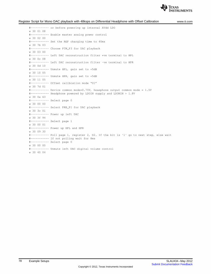
Register Script for Mono DAC playback with 48ksps on Differential Headphone with Offset Calibration www.ti.com
#----------- or before powering up internal AVdd LDOw 30 01 08#----------- Enable master analog power controlw 30 02 00#----------- Set the REF charging time to 40msw 30 7b 03#----------- Choose PTM_P3 for DAC playbackw 30 03 00#----------- Left DAC reconstruction filter +ve terminal to HPLw 30 0c 08#----------- Left DAC reconstruction filter -ve terminal to HPRw 30 0d 10#----------- Unmute HPL, gain set to +5dBw 30 10 05#----------- Unmute HPR, gain set to +5dBw 30 11 05#----------- Offset calibration mode “01”w 30 7d 01#----------- Device common mode=0.75V, heaephone output common mode = 1.5V#----------- Headphone powered by LDOIN supply and LDONIN > 1.8Vw 30 0a 63#----------- Select page 0w 30 00 00#----------- Select PRB_P1 for DAC playbackw 30 3c 01#----------- Power up left DACw 30 3f 94#----------- Select page 1w 30 00 01#----------- Power up HPL and HPRw 30 09 30#----------- Poll page 1, register 2, D2. If the bit is '1' go to next step, else wait#----------- If not polling wait for 8ms#----------- Select page 0w 30 00 00#----------- Unmute left DAC digital volume controlw 30 40 04
78 Example Setups SLAU434–May 2012Submit Documentation Feedback
Copyright © 2012, Texas Instruments Incorporated
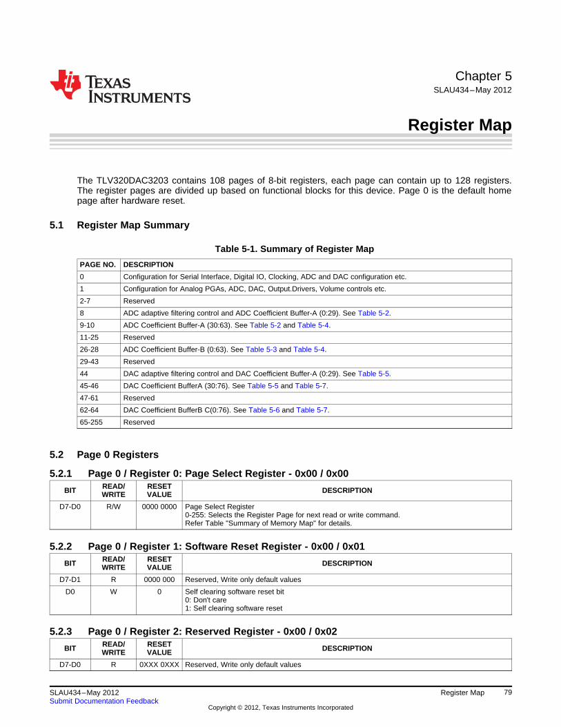
Chapter 5SLAU434–May 2012
Register Map
The TLV320DAC3203 contains 108 pages of 8-bit registers, each page can contain up to 128 registers.The register pages are divided up based on functional blocks for this device. Page 0 is the default homepage after hardware reset.
5.1 Register Map Summary
Table 5-1. Summary of Register Map
PAGE NO. DESCRIPTION
0 Configuration for Serial Interface, Digital IO, Clocking, ADC and DAC configuration etc.
1 Configuration for Analog PGAs, ADC, DAC, Output.Drivers, Volume controls etc.
2-7 Reserved
8 ADC adaptive filtering control and ADC Coefficient Buffer-A (0:29). See Table 5-2.
9-10 ADC Coefficient Buffer-A (30:63). See Table 5-2 and Table 5-4.
11-25 Reserved
26-28 ADC Coefficient Buffer-B (0:63). See Table 5-3 and Table 5-4.
29-43 Reserved
44 DAC adaptive filtering control and DAC Coefficient Buffer-A (0:29). See Table 5-5.
45-46 DAC Coefficient BufferA (30:76). See Table 5-5 and Table 5-7.
47-61 Reserved
62-64 DAC Coefficient BufferB C(0:76). See Table 5-6 and Table 5-7.
65-255 Reserved
5.2 Page 0 Registers
5.2.1 Page 0 / Register 0: Page Select Register - 0x00 / 0x00READ/ RESETBIT DESCRIPTIONWRITE VALUE
D7-D0 R/W 0000 0000 Page Select Register0-255: Selects the Register Page for next read or write command.Refer Table "Summary of Memory Map" for details.
5.2.2 Page 0 / Register 1: Software Reset Register - 0x00 / 0x01READ/ RESETBIT DESCRIPTIONWRITE VALUE
D7-D1 R 0000 000 Reserved, Write only default values
D0 W 0 Self clearing software reset bit0: Don't care1: Self clearing software reset
5.2.3 Page 0 / Register 2: Reserved Register - 0x00 / 0x02READ/ RESETBIT DESCRIPTIONWRITE VALUE
D7-D0 R 0XXX 0XXX Reserved, Write only default values
79SLAU434–May 2012 Register MapSubmit Documentation Feedback
Copyright © 2012, Texas Instruments Incorporated

Page 0 Registers www.ti.com
5.2.4 Page 0 / Register 3: Reserved Register - 0x00 / 0x03READ/ RESETBIT DESCRIPTIONWRITE VALUE
D7-D0 R 0000 0000 Reserved, Write only default values to this register
5.2.5 Page 0 / Register 4: Clock Setting Register 1, Multiplexers - 0x00 / 0x04READ/ RESETBIT DESCRIPTIONWRITE VALUE
D7 R 0 Reserved, Write only default values
D6 R/W 0 Select PLL Range0: Low PLL Clock Range1: High PLL Clock Range
D5-D4 R 00 Reserved, Write only default values any other value than reset value.
D3-D2 R/W 00 Select PLL Input Clock00: MCLK pin is input to PLL01: BCLK pin is input to PLL10: GPIO pin is input to PLL (** Availble only for WCSP Package)11: DIN pin is input to PLL
D1-D0 R/W 00 Select CODEC_CLKIN00: MCLK pin is CODEC_CLKIN01: BCLK pin is CODEC_CLKIN10: GPIO pin is CODEC_CLKIN (** Availble only for WCSP Package)11: PLL Clock is CODEC_CLKIN
5.2.6 Page 0 / Register 5: Clock Setting Register 2, PLL P&R Values - 0x00 / 0x05READ/ RESETBIT DESCRIPTIONWRITE VALUE
D7 R/W 0 PLL Power Up0: PLL is powered down1: PLL is powered up
D6-D4 R/W 001 PLL divider P Value000: P=8001: P=1010: P=2…110: P=6111: P=7
D3-D0 R/W 0001 PLL divider R Value000: Reserved, do not use001: R=1010: R=2011: R=3100: R=4101…111: Reserved, do not use
5.2.7 Page 0 / Register 6: Clock Setting Register 3, PLL J Values - 0x00 / 0x06READ/ RESETBIT DESCRIPTIONWRITE VALUE
D7-D6 R 00 Reserved. Write only default values any value other than default
D5-D0 R/W 00 0100 PLL divider J value00 0000…00 0011: Do not use00 0100: J=400 0101: J=5…11 1110: J=6211 1111: J=63
5.2.8 Page 0 / Register 7: Clock Setting Register 4, PLL D Values (MSB) - 0x00 / 0x07READ/ RESETBIT DESCRIPTIONWRITE VALUE
D7-D6 R 00 Reserved. Write only default values any value other than default
80 Register Map SLAU434–May 2012Submit Documentation Feedback
Copyright © 2012, Texas Instruments Incorporated
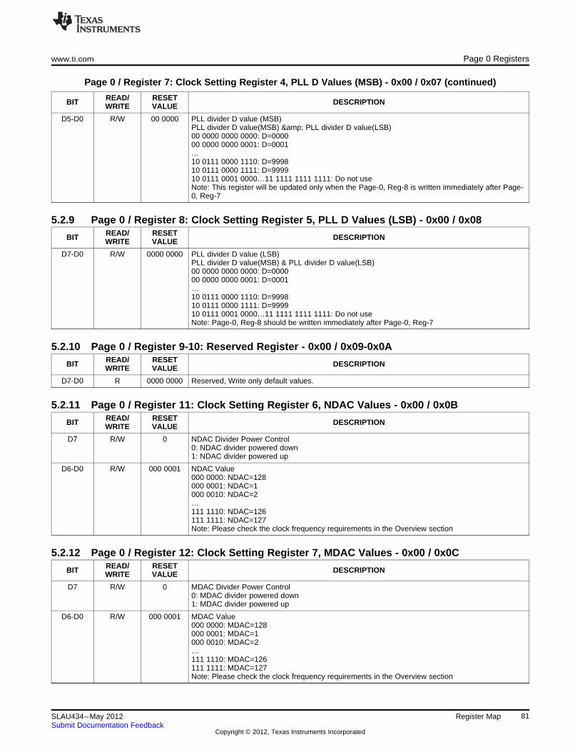
www.ti.com Page 0 Registers
Page 0 / Register 7: Clock Setting Register 4, PLL D Values (MSB) - 0x00 / 0x07 (continued)
READ/ RESETBIT DESCRIPTIONWRITE VALUE
D5-D0 R/W 00 0000 PLL divider D value (MSB)PLL divider D value(MSB) & PLL divider D value(LSB)00 0000 0000 0000: D=000000 0000 0000 0001: D=0001…10 0111 0000 1110: D=999810 0111 0000 1111: D=999910 0111 0001 0000…11 1111 1111 1111: Do not useNote: This register will be updated only when the Page-0, Reg-8 is written immediately after Page-0, Reg-7
5.2.9 Page 0 / Register 8: Clock Setting Register 5, PLL D Values (LSB) - 0x00 / 0x08READ/ RESETBIT DESCRIPTIONWRITE VALUE
D7-D0 R/W 0000 0000 PLL divider D value (LSB)PLL divider D value(MSB) & PLL divider D value(LSB)00 0000 0000 0000: D=000000 0000 0000 0001: D=0001…10 0111 0000 1110: D=999810 0111 0000 1111: D=999910 0111 0001 0000…11 1111 1111 1111: Do not useNote: Page-0, Reg-8 should be written immediately after Page-0, Reg-7
5.2.10 Page 0 / Register 9-10: Reserved Register - 0x00 / 0x09-0x0AREAD/ RESETBIT DESCRIPTIONWRITE VALUE
D7-D0 R 0000 0000 Reserved, Write only default values.
5.2.11 Page 0 / Register 11: Clock Setting Register 6, NDAC Values - 0x00 / 0x0BREAD/ RESETBIT DESCRIPTIONWRITE VALUE
D7 R/W 0 NDAC Divider Power Control0: NDAC divider powered down1: NDAC divider powered up
D6-D0 R/W 000 0001 NDAC Value000 0000: NDAC=128000 0001: NDAC=1000 0010: NDAC=2…111 1110: NDAC=126111 1111: NDAC=127Note: Please check the clock frequency requirements in the Overview section
5.2.12 Page 0 / Register 12: Clock Setting Register 7, MDAC Values - 0x00 / 0x0CREAD/ RESETBIT DESCRIPTIONWRITE VALUE
D7 R/W 0 MDAC Divider Power Control0: MDAC divider powered down1: MDAC divider powered up
D6-D0 R/W 000 0001 MDAC Value000 0000: MDAC=128000 0001: MDAC=1000 0010: MDAC=2…111 1110: MDAC=126111 1111: MDAC=127Note: Please check the clock frequency requirements in the Overview section
81SLAU434–May 2012 Register MapSubmit Documentation Feedback
Copyright © 2012, Texas Instruments Incorporated
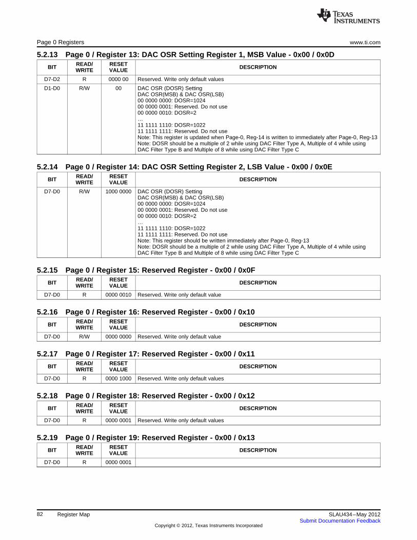
Page 0 Registers www.ti.com
5.2.13 Page 0 / Register 13: DAC OSR Setting Register 1, MSB Value - 0x00 / 0x0DREAD/ RESETBIT DESCRIPTIONWRITE VALUE
D7-D2 R 0000 00 Reserved. Write only default values
D1-D0 R/W 00 DAC OSR (DOSR) SettingDAC OSR(MSB) & DAC OSR(LSB)00 0000 0000: DOSR=102400 0000 0001: Reserved. Do not use00 0000 0010: DOSR=2…11 1111 1110: DOSR=102211 1111 1111: Reserved. Do not useNote: This register is updated when Page-0, Reg-14 is written to immediately after Page-0, Reg-13Note: DOSR should be a multiple of 2 while using DAC Filter Type A, Multiple of 4 while usingDAC Filter Type B and Multiple of 8 while using DAC Filter Type C
5.2.14 Page 0 / Register 14: DAC OSR Setting Register 2, LSB Value - 0x00 / 0x0EREAD/ RESETBIT DESCRIPTIONWRITE VALUE
D7-D0 R/W 1000 0000 DAC OSR (DOSR) SettingDAC OSR(MSB) & DAC OSR(LSB)00 0000 0000: DOSR=102400 0000 0001: Reserved. Do not use00 0000 0010: DOSR=2…11 1111 1110: DOSR=102211 1111 1111: Reserved. Do not useNote: This register should be written immediately after Page-0, Reg-13Note: DOSR should be a multiple of 2 while using DAC Filter Type A, Multiple of 4 while usingDAC Filter Type B and Multiple of 8 while using DAC Filter Type C
5.2.15 Page 0 / Register 15: Reserved Register - 0x00 / 0x0FREAD/ RESETBIT DESCRIPTIONWRITE VALUE
D7-D0 R 0000 0010 Reserved. Write only default value
5.2.16 Page 0 / Register 16: Reserved Register - 0x00 / 0x10READ/ RESETBIT DESCRIPTIONWRITE VALUE
D7-D0 R/W 0000 0000 Reserved. Write only default value
5.2.17 Page 0 / Register 17: Reserved Register - 0x00 / 0x11READ/ RESETBIT DESCRIPTIONWRITE VALUE
D7-D0 R 0000 1000 Reserved. Write only default values
5.2.18 Page 0 / Register 18: Reserved Register - 0x00 / 0x12READ/ RESETBIT DESCRIPTIONWRITE VALUE
D7-D0 R 0000 0001 Reserved. Write only default values
5.2.19 Page 0 / Register 19: Reserved Register - 0x00 / 0x13READ/ RESETBIT DESCRIPTIONWRITE VALUE
D7-D0 R 0000 0001
82 Register Map SLAU434–May 2012Submit Documentation Feedback
Copyright © 2012, Texas Instruments Incorporated

www.ti.com Page 0 Registers
5.2.20 Page 0 / Register 20: ADC Oversampling (AOSR) Register - 0x00 / 0x14READ/ RESETBIT DESCRIPTIONWRITE VALUE
D7-D0 R 1000 0000 ADC Oversampling Value0000 0000: ADC AOSR = 2560000 0001-0001 1111: Reserved. Do not use0010 0000: ADC AOSR=32 (Use with PRB_R13 to PRB_R18, ADC Filter Type C)0010 0001-0011 1111: Reserved.Do not use0100 0000: AOSR=64 (Use with PRB_R1 to PRB_R12, ADC Filter Type A or B)0100 0001-0111 1111: Reserved. Do not use1000 0000: AOSR=128(Use with PRB_R1 to PRB_R6, ADC Filter Type A)1000 0001-1111 1111: Reserved. Do not use
5.2.21 Page 0 / Register 21: Reserved Register - 0x00 / 0x15READ/ RESETBIT DESCRIPTIONWRITE VALUE
D7-D0 R 0000 0001 Reserved. Write only default values
5.2.22 Page 0 / Register 22: Reserved Register - 0x00 / 0x16READ/ RESETBIT DESCRIPTIONWRITE VALUE
D7-D0 R 0000 0000 Reserved. Write only default values
5.2.23 Page 0 / Register 23: Reserved Register - 0x00 / 0x17READ/ RESETBIT DESCRIPTIONWRITE VALUE
D7-D0 R 0000 0100 Reserved. Write only default values
5.2.24 Page 0 / Register 24: Reserved Register - 0x00 / 0x18READ/ RESETBIT DESCRIPTIONWRITE VALUE
D7-D0 R 0000 0000 Reserved. Write only default values
5.2.25 Page 0 / Register 25: Clock Setting Register 8, Multiplexers - 0x00 / 0x19READ/ RESETBIT DESCRIPTIONWRITE VALUE
D7-D3 R 0000 0 Reserved. Write only default values
D2-D0 R/W 000 CDIV_CLKIN Clock Selection000: CDIV_CLKIN= MCLK001: CDIV_CLKIN= BCLK010: CDIV_CLKIN=DIN011: CDIV_CLKIN=PLL_CLK100: CDIV_CLKIN=DAC_CLK101: CDIV_CLKIN=DAC_MOD_CLK110-111: Reserved
5.2.26 Page 0 / Register 26: Clock Setting Register 9, CLKOUT M divider value - 0x00 / 0x1AREAD/ RESETBIT DESCRIPTIONWRITE VALUE
D7 R/W 0 CLKOUT M divider power control0: CLKOUT M divider powered down1: CLKOUT M divider powered up
D6-D0 R/W 000 0001 CLKOUT M divider value000 0000: CLKOUT M divider = 128000 0001: CLKOUT M divider = 1000 0010: CLKOUT M divider = 2…111 1110: CLKOUT M divider = 126111 1111: CLKOUT M divider = 127Note: Please check the clock frequency requirements in the application overview section
83SLAU434–May 2012 Register MapSubmit Documentation Feedback
Copyright © 2012, Texas Instruments Incorporated
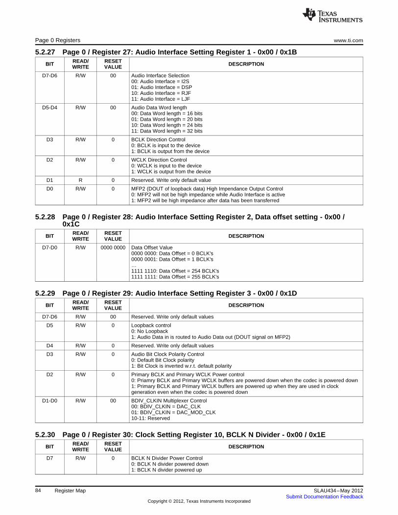
Page 0 Registers www.ti.com
5.2.27 Page 0 / Register 27: Audio Interface Setting Register 1 - 0x00 / 0x1BREAD/ RESETBIT DESCRIPTIONWRITE VALUE
D7-D6 R/W 00 Audio Interface Selection00: Audio Interface = I2S01: Audio Interface = DSP10: Audio Interface = RJF11: Audio Interface = LJF
D5-D4 R/W 00 Audio Data Word length00: Data Word length = 16 bits01: Data Word length = 20 bits10: Data Word length = 24 bits11: Data Word length = 32 bits
D3 R/W 0 BCLK Direction Control0: BCLK is input to the device1: BCLK is output from the device
D2 R/W 0 WCLK Direction Control0: WCLK is input to the device1: WCLK is output from the device
D1 R 0 Reserved. Write only default value
D0 R/W 0 MFP2 (DOUT of loopback data) High Impendance Output Control0: MFP2 will not be high impedance while Audio Interface is active1: MFP2 will be high impedance after data has been transferred
5.2.28 Page 0 / Register 28: Audio Interface Setting Register 2, Data offset setting - 0x00 /0x1C
READ/ RESETBIT DESCRIPTIONWRITE VALUE
D7-D0 R/W 0000 0000 Data Offset Value0000 0000: Data Offset = 0 BCLK's0000 0001: Data Offset = 1 BCLK's…1111 1110: Data Offset = 254 BCLK's1111 1111: Data Offset = 255 BCLK's
5.2.29 Page 0 / Register 29: Audio Interface Setting Register 3 - 0x00 / 0x1DREAD/ RESETBIT DESCRIPTIONWRITE VALUE
D7-D6 R/W 00 Reserved. Write only default values
D5 R/W 0 Loopback control0: No Loopback1: Audio Data in is routed to Audio Data out (DOUT signal on MFP2)
D4 R/W 0 Reserved. Write only default values
D3 R/W 0 Audio Bit Clock Polarity Control0: Default Bit Clock polarity1: Bit Clock is inverted w.r.t. default polarity
D2 R/W 0 Primary BCLK and Primary WCLK Power control0: Priamry BCLK and Primary WCLK buffers are powered down when the codec is powered down1: Primary BCLK and Primary WCLK buffers are powered up when they are used in clockgeneration even when the codec is powered down
D1-D0 R/W 00 BDIV_CLKIN Multiplexer Control00: BDIV_CLKIN = DAC_CLK01: BDIV_CLKIN = DAC_MOD_CLK10-11: Reserved
5.2.30 Page 0 / Register 30: Clock Setting Register 10, BCLK N Divider - 0x00 / 0x1EREAD/ RESETBIT DESCRIPTIONWRITE VALUE
D7 R/W 0 BCLK N Divider Power Control0: BCLK N divider powered down1: BCLK N divider powered up
84 Register Map SLAU434–May 2012Submit Documentation Feedback
Copyright © 2012, Texas Instruments Incorporated

www.ti.com Page 0 Registers
Page 0 / Register 30: Clock Setting Register 10, BCLK N Divider - 0x00 / 0x1E (continued)
READ/ RESETBIT DESCRIPTIONWRITE VALUE
D6-D0 R/W 000 0001 BCLK N Divider value0000 0000: BCLK N divider = 1280000 0001: BCLK N divider = 1…1111 1110: BCLK N divider = 1261111 1111: BCLK N divider = 127
5.2.31 Page 0 / Register 31: Audio Interface Setting Register 4, Secondary Audio Interface -0x00 / 0x1F
READ/ RESETBIT DESCRIPTIONWRITE VALUE
D7 R 0 Reserved. Write only default values
D6-D5 R/W 00 Secondary Bit Clock Multiplexer00: Secondary Bit Clock = GPIO (** Availble only for WCSP Package)01: Secondary Bit Clock = SCLK10: Secondary Bit Clock = MISO11: Secondary Bit Clock = DOUT
D4-D3 R/W 00 Secondary Word Clock Multiplexer00: Secondary Word Clock = GPIO (** Availble only for WCSP Package)01: Secondary Word Clock = SCLK10: Secondary Word Clock = MISO11: Secondary Word Clock = DOUT
D2-D1 R/W 00 ADC Word Clock Multiplexer00: ADC Word Clock = GPIO (** Availble only for WCSP Package)01: ADC Word Clock = SCLK10: ADC Word Clock = MISO11: Do not use
D0 R/W 0 Secondary Data Input Multiplexer0: Secondary Data Input = GPIO (** Availble only for WCSP Package)1: Secondary Data Input = SCLK
5.2.32 Page 0 / Register 32: Audio Interface Setting Register 5 - 0x00 / 0x20READ/ RESETBIT DESCRIPTIONWRITE VALUE
D7-D4 R 0000 Reserved. Write only default values
D3 R/W 0 Primary / Secondary Bit Clock Control0: Primary Bit Clock(BCLK) is used for Audio Interface and Clocking1: Secondary Bit Clock is used for Audio Interface and Clocking
D2 R/W 0 Primary / Secondary Word Clock Control0: Primary Word Clock(WCLK) is used for Audio Interface1: Secondary Word Clock is used for Audio Interface
D1 R/W 0 Reserved. Write only default value
D0 R/W 0 Audio Data In Control0: DIN is used for Audio Data In1: Secondary Data In is used for Audio Data In
5.2.33 Page 0 / Register 33: Audio Interface Setting Register 6 - 0x00 / 0x21READ/ RESETBIT DESCRIPTIONWRITE VALUE
D7 R/W 0 BCLK Output Control0: BCLK Output = Generated Primary Bit Clock1: BCLK Output = Secondary Bit Clock Input
D6 R/W 0 Secondary Bit Clock Output Control0: Secondary Bit Clock = BCLK input1: Secondary Bit Clock = Generated Primary Bit Clock
85SLAU434–May 2012 Register MapSubmit Documentation Feedback
Copyright © 2012, Texas Instruments Incorporated

Page 0 Registers www.ti.com
Page 0 / Register 33: Audio Interface Setting Register 6 - 0x00 / 0x21 (continued)
READ/ RESETBIT DESCRIPTIONWRITE VALUE
D5-D4 R/W 00 WCLK Output Control00: WCLK Output = Generated DAC_FS01: Reserved. Do not use10: WCLK Output = Secondary Word Clock Input11: Reserved. Do not use
D3-D2 R/W 00 Secondary Word Clock Output Control00: Secondary Word Clock output = WCLK input01: Secondary Word Clock output = Generated DAC_FS10-11: Reserved Do not use
D1 R/W 0 Primary Data Out output control (MFP2)0: no Data output1: Primary Data Output = Secondary Data Input (Loopback)
D0 R/W 0 Secondary Data Out output control (MFP4)0: Secondary Data Output = DIN input (Loopback)1: no Data output
5.2.34 Page 0 / Register 34: Digital Interface Misc. Setting Register - 0x00 / 0x22READ/ RESETBIT DESCRIPTIONWRITE VALUE
D7 R 0 Reserved. Write only default value
D6 R 0 Reserved. Write only default value
D5 R/W 0 I2C General Call Address Configuration0: I2C General Call Address will be ignored1: I2C General Call Address accepted
D4-D0 R 0 0000 Reserved. Write only default values
5.2.35 Page 0 / Register 35-36: Reserved Register - 0x00 / 0x23-0x24READ/ RESETBIT DESCRIPTIONWRITE VALUE
D7-D0 R 0000 0000 Reserved. Write only default value
5.2.36 Page 0 / Register 37: DAC Flag Register 1 - 0x00 / 0x25READ/ RESETBIT DESCRIPTIONWRITE VALUE
D7 R 0 Left DAC Power Status Flag0: Left DAC Powered Down1: Left DAC Powered Up
D6 R 0 Reserved.
D5 R 0 Left Headphone Driver (HPL) Power Status Flag0: HPL Powered Down1: HPL Powered Up
D4 R 0 Reserved.
D3 R 0 Right DAC Power Status Flag0: Right DAC Powered Down1: Right DAC Powered Up
D2 R 0 Reserved.
D1 R 0 Right Headphone Driver (HPR) Power Status Flag0: HPR Powered Down1: HPR Powered Up
D0 R 0 Reserved.
5.2.37 Page 0 / Register 38: DAC Flag Register 2 - 0x00 / 0x26READ/ RESETBIT DESCRIPTIONWRITE VALUE
D7-D5 R 000 Reserved.
86 Register Map SLAU434–May 2012Submit Documentation Feedback
Copyright © 2012, Texas Instruments Incorporated

www.ti.com Page 0 Registers
Page 0 / Register 38: DAC Flag Register 2 - 0x00 / 0x26 (continued)
READ/ RESETBIT DESCRIPTIONWRITE VALUE
D4 R 0 Left DAC PGA Status Flag0: Gain applied in Left DAC PGA is not equal to Gain programmed in Control Register1: Gain applied in Left DAC PGA is equal to Gain programmed in Control Register
D3-D1 R 000 Reserved.
D0 R 0 Right DAC PGA Status Flag0: Gain applied in Right DAC PGA is not equal to Gain programmed in Control Register1: Gain applied in Right DAC PGA is equal to Gain programmed in Control Register
5.2.38 Page 0 / Register 39-41: Reserved Register - 0x00 / 0x27-0x29READ/ RESETBIT DESCRIPTIONWRITE VALUE
D7-D0 R 0000 0000 Reserved. Write only default values
5.2.39 Page 0 / Register 42: Sticky Flag Register 1 - 0x00 / 0x2AREAD/ RESETBIT DESCRIPTIONWRITE VALUE
D7 R 0 Left DAC Overflow Status. This sticky flag will self clear on read0: No overflow in Left DAC1: Overflow has happened in Left DAC since last read of this register
D6 R 0 Right DAC Overflow Status. This sticky flag will self clear on read0: No overflow in Right DAC1: Overflow has happened in Right DAC since last read of this register
D5-D0 R 0 0000 Reserved.
5.2.40 Page 0 / Register 43: Interrupt Flag Register 1 - 0x00 / 0x2BREAD/ RESETBIT DESCRIPTIONWRITE VALUE
D7 R 0 Left DAC Overflow Status.0: No overflow in Left DAC1: Overflow condition is present in Left ADC at the time of reading the register
D6 R 0 Right DAC Overflow Status.0: No overflow in Right DAC1: Overflow condition is present in Right DAC at the time of reading the register
D5-D4 R 00 Reserved.
D3 R 0 Left ADC Overflow Status.0: No overflow in Left ADC1: Overflow condition is present in Left ADC at the time of reading the register
D2 R 0 Right ADC Overflow Status.0: No overflow in Right ADC1: Overflow condition is present in Right ADC at the time of reading the register
5.2.41 Page 0 / Register 44: Sticky Flag Register 2 - 0x00 / 0x2CREAD/ RESETBIT DESCRIPTIONWRITE VALUE
D7 R 0 HPL Over Current Detect Flag0: Over Current not detected on HPL1: Over Current detected on HPL (will be cleared when the register is read)
D6 R 0 HPR Over Current Detect Flag0: Over Current not detected on HPR1: Over Current detected on HPR (will be cleared when the register is read)
D5 R 0 Headset Button Press0: Button Press not detected1: Button Press detected (will be cleared when the register is read)
D4 R 0 Headset Insertion/Removal Detect Flag0: Insertion/Removal event not detected1: Insertion/Removal event detected (will be cleared when the register is read)
87SLAU434–May 2012 Register MapSubmit Documentation Feedback
Copyright © 2012, Texas Instruments Incorporated

Page 0 Registers www.ti.com
Page 0 / Register 44: Sticky Flag Register 2 - 0x00 / 0x2C (continued)
READ/ RESETBIT DESCRIPTIONWRITE VALUE
D3 R 0 Left Channel DRC, Signal Threshold Flag0: Signal Power is below Signal Threshold1: Signal Power exceeded Signal Threshold (will be cleared when the register is read)
D2 R 0 Right Channel DRC, Signal Threshold Flag0: Signal Power is below Signal Threshold1: Signal Power exceeded Signal Threshold (will be cleared when the register is read)
D1-D0 R 00 Reserved.
5.2.42 Page 0 / Register 45: Reserved Register - 0x00 / 0x2DREAD/ RESETBIT DESCRIPTIONWRITE VALUE
D7-D0 R 0000 0000 Reserved. Write only default values
5.2.43 Page 0 / Register 46: Interrupt Flag Register 2 - 0x00 / 0x2EREAD/ RESETBIT DESCRIPTIONWRITE VALUE
D7 R 0 HPL Over Current Detect Flag0: Over Current not detected on HPL1: Over Current detected on HPL
D6 R 0 HPR Over Current Detect Flag0: Over Current not detected on HPR1: Over Current detected on HPR
D5 R 0 Headset Button Press0: Button Press not detected1: Button Press detected
D4 R 0 Headset Insertion/Removal Detect Flag0: Headset removal detected1: Headset insertion detected
D3 R 0 Left Channel DRC, Signal Threshold Flag0: Signal Power is below Signal Threshold1: Signal Power exceeded Signal Threshold
D2 R 0 Right Channel DRC, Signal Threshold Flag0: Signal Power is below Signal Threshold1: Signal Power exceeded Signal Threshold
D1-D0 R 00 Reserved.
5.2.44 Page 0 / Register 47: Reserved Register - 0x00 / 0x2FREAD/ RESETBIT DESCRIPTIONWRITE VALUE
D7-D5 R 0000 0000 Reserved. Write only default values
5.2.45 Page 0 / Register 48: INT1 Interrupt Control Register - 0x00 / 0x30READ/ RESETBIT DESCRIPTIONWRITE VALUE
D7 R/W 0 INT1 Interrupt for Headset Insertion Event0: Headset Insertion event will not generate a INT1 interrupt1: Headset Insertion even will generate a INT1 interrupt
D6 R/W 0 INT1 Interrupt for Button Press Event0: Button Press event will not generate a INT1 interrupt1: Button Press event will generate a INT1 interrupt
D5 R/W 0 INT1 Interrupt for DAC DRC Signal Threshold0: DAC DRC Signal Power exceeding Signal Threshold will not generate a INT1 interrupt1: DAC DRC Signal Power exceeding Signal Threshold for either of Left or Right Channel willgenerate a INT1 interrupt.Read Page-0, Register-44 to distinguish between Left or Right Channel
D4 R 0 Reserved. Write only default value
88 Register Map SLAU434–May 2012Submit Documentation Feedback
Copyright © 2012, Texas Instruments Incorporated

www.ti.com Page 0 Registers
Page 0 / Register 48: INT1 Interrupt Control Register - 0x00 / 0x30 (continued)
READ/ RESETBIT DESCRIPTIONWRITE VALUE
D3 R/W 0 INT1 Interrupt for Over Current Condition0: Headphone Over Current condition will not generate a INT1 interrupt.1: Headphone Over Current condition on either off Left or Right Channels will generate a INT1interrupt.Read Page-0, Register-44 to distinguish between HPL and HPR
D2 R/W 0 INT1 Interrupt for overflow event0: ADC or DAC data overflows does not result in a INT1 interrupt1: ADC or DAC data overflow will result in a INT1 interrupt.Read Page-0, Register-42 to distinguish between ADC or DAC data overflow
D1 R 0 Reserved. Write only default value
D0 R/W 0 INT1 pulse control0: INT1 is active high interrupt of 1 pulse of approx. 2ms duration1: INT1 is active high interrupt of multiple pulses, each of duration 2ms. To stop the pulse train,read Page-0, Reg-42d, 44d or 45d
5.2.46 Page 0 / Register 49: INT2 Interrupt Control Register - 0x00 / 0x31READ/ RESETBIT DESCRIPTIONWRITE VALUE
D7 R/W 0 INT2 Interrupt for Headset Insertion Event0: Headset Insertion event will not generate a INT2 interrupt1: Headset Insertion even will generate a INT2 interrupt
D6 R/W 0 INT2 Interrupt for Button Press Event0: Button Press event will not generate a INT2 interrupt1: Button Press event will generate a INT2 interrupt
D5 R/W 0 INT2 Interrupt for DAC DRC Signal Threshold0: DAC DRC Signal Power exceeding Signal Threshold will not generate a INT2 interrupt1: DAC DRC Signal Power exceeding Signal Threshold for either of Left or Right Channel willgenerate a INT2 interrupt.Read Page-0, Register-44 to distinguish between Left or Right Channel
D4 R 0 Reserved. Write only default value
D3 R/W 0 INT2 Interrupt for Over Current Condition0: Headphone Over Current condition will not generate a INT2 interrupt.1: Headphone Over Current condition on either off Left or Right Channels will generate a INT2interrupt.Read Page-0, Register-44 to distinguish between HPL and HPR
D2 R/W 0 INT2 Interrupt for overflow event0: DAC data overflow will not result in a INT2 interrupt1: DAC data overflow will result in a INT2 interrupt.Read Page-0, Register-42 on DAC data overflow details
D1 R 0 Reserved. Write only default value
D0 R/W 0 INT2 pulse control0: INT2 is active high interrupt of 1 pulse of approx. 2ms duration1: INT2 is active high interrupt of multiple pulses, each of duration 2ms. To stop the pulse train,read Page-0, Reg-42d, 44d and 45d
5.2.47 Page 0 / Register 50-51: Reserved Register - 0x00 / 0x32-0x33READ/ RESETBIT DESCRIPTIONWRITE VALUE
D7-D0 R 0000 0000 Reserved. Write only default values
5.2.48 Page 0 / Register 52: GPIO/MFP5 Control Register (** Availble only for WCSP Package) -0x00 / 0x34
READ/ RESETBIT DESCRIPTIONWRITE VALUE
D7-D6 R 00 Reserved. Write only default values
89SLAU434–May 2012 Register MapSubmit Documentation Feedback
Copyright © 2012, Texas Instruments Incorporated
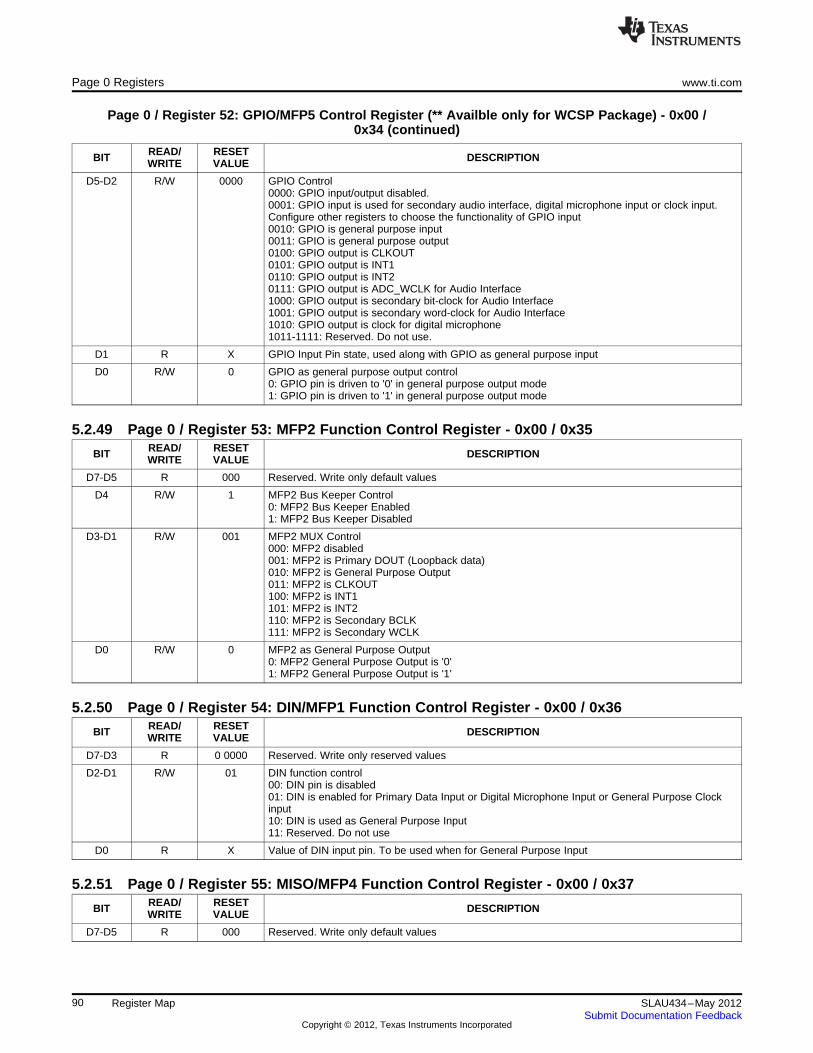
Page 0 Registers www.ti.com
Page 0 / Register 52: GPIO/MFP5 Control Register (** Availble only for WCSP Package) - 0x00 /0x34 (continued)
READ/ RESETBIT DESCRIPTIONWRITE VALUE
D5-D2 R/W 0000 GPIO Control0000: GPIO input/output disabled.0001: GPIO input is used for secondary audio interface, digital microphone input or clock input.Configure other registers to choose the functionality of GPIO input0010: GPIO is general purpose input0011: GPIO is general purpose output0100: GPIO output is CLKOUT0101: GPIO output is INT10110: GPIO output is INT20111: GPIO output is ADC_WCLK for Audio Interface1000: GPIO output is secondary bit-clock for Audio Interface1001: GPIO output is secondary word-clock for Audio Interface1010: GPIO output is clock for digital microphone1011-1111: Reserved. Do not use.
D1 R X GPIO Input Pin state, used along with GPIO as general purpose input
D0 R/W 0 GPIO as general purpose output control0: GPIO pin is driven to '0' in general purpose output mode1: GPIO pin is driven to '1' in general purpose output mode
5.2.49 Page 0 / Register 53: MFP2 Function Control Register - 0x00 / 0x35READ/ RESETBIT DESCRIPTIONWRITE VALUE
D7-D5 R 000 Reserved. Write only default values
D4 R/W 1 MFP2 Bus Keeper Control0: MFP2 Bus Keeper Enabled1: MFP2 Bus Keeper Disabled
D3-D1 R/W 001 MFP2 MUX Control000: MFP2 disabled001: MFP2 is Primary DOUT (Loopback data)010: MFP2 is General Purpose Output011: MFP2 is CLKOUT100: MFP2 is INT1101: MFP2 is INT2110: MFP2 is Secondary BCLK111: MFP2 is Secondary WCLK
D0 R/W 0 MFP2 as General Purpose Output0: MFP2 General Purpose Output is '0'1: MFP2 General Purpose Output is '1'
5.2.50 Page 0 / Register 54: DIN/MFP1 Function Control Register - 0x00 / 0x36READ/ RESETBIT DESCRIPTIONWRITE VALUE
D7-D3 R 0 0000 Reserved. Write only reserved values
D2-D1 R/W 01 DIN function control00: DIN pin is disabled01: DIN is enabled for Primary Data Input or Digital Microphone Input or General Purpose Clockinput10: DIN is used as General Purpose Input11: Reserved. Do not use
D0 R X Value of DIN input pin. To be used when for General Purpose Input
5.2.51 Page 0 / Register 55: MISO/MFP4 Function Control Register - 0x00 / 0x37READ/ RESETBIT DESCRIPTIONWRITE VALUE
D7-D5 R 000 Reserved. Write only default values
90 Register Map SLAU434–May 2012Submit Documentation Feedback
Copyright © 2012, Texas Instruments Incorporated
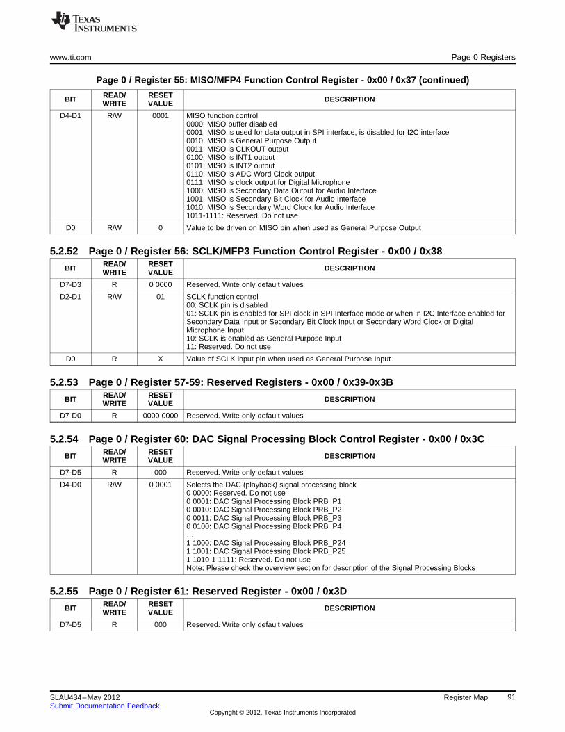
www.ti.com Page 0 Registers
Page 0 / Register 55: MISO/MFP4 Function Control Register - 0x00 / 0x37 (continued)
READ/ RESETBIT DESCRIPTIONWRITE VALUE
D4-D1 R/W 0001 MISO function control0000: MISO buffer disabled0001: MISO is used for data output in SPI interface, is disabled for I2C interface0010: MISO is General Purpose Output0011: MISO is CLKOUT output0100: MISO is INT1 output0101: MISO is INT2 output0110: MISO is ADC Word Clock output0111: MISO is clock output for Digital Microphone1000: MISO is Secondary Data Output for Audio Interface1001: MISO is Secondary Bit Clock for Audio Interface1010: MISO is Secondary Word Clock for Audio Interface1011-1111: Reserved. Do not use
D0 R/W 0 Value to be driven on MISO pin when used as General Purpose Output
5.2.52 Page 0 / Register 56: SCLK/MFP3 Function Control Register - 0x00 / 0x38READ/ RESETBIT DESCRIPTIONWRITE VALUE
D7-D3 R 0 0000 Reserved. Write only default values
D2-D1 R/W 01 SCLK function control00: SCLK pin is disabled01: SCLK pin is enabled for SPI clock in SPI Interface mode or when in I2C Interface enabled forSecondary Data Input or Secondary Bit Clock Input or Secondary Word Clock or DigitalMicrophone Input10: SCLK is enabled as General Purpose Input11: Reserved. Do not use
D0 R X Value of SCLK input pin when used as General Purpose Input
5.2.53 Page 0 / Register 57-59: Reserved Registers - 0x00 / 0x39-0x3BREAD/ RESETBIT DESCRIPTIONWRITE VALUE
D7-D0 R 0000 0000 Reserved. Write only default values
5.2.54 Page 0 / Register 60: DAC Signal Processing Block Control Register - 0x00 / 0x3CREAD/ RESETBIT DESCRIPTIONWRITE VALUE
D7-D5 R 000 Reserved. Write only default values
D4-D0 R/W 0 0001 Selects the DAC (playback) signal processing block0 0000: Reserved. Do not use0 0001: DAC Signal Processing Block PRB_P10 0010: DAC Signal Processing Block PRB_P20 0011: DAC Signal Processing Block PRB_P30 0100: DAC Signal Processing Block PRB_P4…1 1000: DAC Signal Processing Block PRB_P241 1001: DAC Signal Processing Block PRB_P251 1010-1 1111: Reserved. Do not useNote; Please check the overview section for description of the Signal Processing Blocks
5.2.55 Page 0 / Register 61: Reserved Register - 0x00 / 0x3DREAD/ RESETBIT DESCRIPTIONWRITE VALUE
D7-D5 R 000 Reserved. Write only default values
91SLAU434–May 2012 Register MapSubmit Documentation Feedback
Copyright © 2012, Texas Instruments Incorporated

Page 0 Registers www.ti.com
Page 0 / Register 61: Reserved Register - 0x00 / 0x3D (continued)
READ/ RESETBIT DESCRIPTIONWRITE VALUE
D4-D0 R/W 0 0001 0 0000: Reserved. Do not use0 0001: ADC Singal Processing Block PRB_R10 0010: ADC Signal Processing Block PRB_R20 0011: ADC Signal Processing Block PRB_R30 0100: ADC Signal Processing Block PRB_R4…1 0001: ADC Signal Processing Block PRB_R171 0010: ADC Signal Processing Block PRB_R181 0010-1 1111: Reserved. Do not useNote: Please check the overview section for description of the Signal Processing Modes
5.2.56 Page 0 / Register 62: Reserved Register - 0x00 / 0x3EREAD/ RESETBIT DESCRIPTIONWRITE VALUE
D7-D0 R 0000 0000 Reserved. Write only default values
5.2.57 Page 0 / Register 63: DAC Channel Setup Register 1 - 0x00 / 0x3FREAD/ RESETBIT DESCRIPTIONWRITE VALUE
D7 R/W 0 Left DAC Channel Power Control0: Left DAC Channel Powered Down1: Left DAC Channel Powered Up
D6 R/W 0 Right DAC Channel Power Control0: Right DAC Channel Powered Down1: Right DAC Channel Powered Up
D5-D4 R/W 01 Left DAC Data path Control00: Left DAC data is disabled01: Left DAC data Left Channel Audio Interface Data10: Left DAC data is Right Channel Audio Interface Data11: Left DAC data is Mono Mix of Left and Right Channel Audio Interface Data
D3-D2 R/W 01 Right DAC Data path Control00: Right DAC data is disabled01: Right DAC data Right Channel Audio Interface Data10: Right DAC data is Left Channel Audio Interface Data11: Right DAC data is Mono Mix of Left and Right Channel Audio Interface Data
D1-D0 R/W 00 DAC Channel Volume Control's Soft-Step control00: Soft-Stepping is 1 step per 1 DAC Word Clock01: Soft-Stepping is 1 step per 2 DAC Word Clocks10: Soft-Stepping is disabled11: Reserved. Do not use
5.2.58 Page 0 / Register 64: DAC Channel Setup Register 2 - 0x00 / 0x40READ/ RESETBIT DESCRIPTIONWRITE VALUE
D7 R/W 0 Right Modulator Output Control0: When Right DAC Channel is powered down, the data is zero.1: When Right DAC Channel is powered down, the data is inverted version of Left DAC ModulatorOutput. Can be used when differential mono output is used
D6-D4 R/W 000 DAC Auto Mute Control000: Auto Mute disabled001: DAC is auto muted if input data is DC for more than 100 consecutive inputs010: DAC is auto muted if input data is DC for more than 200 consecutive inputs011: DAC is auto muted if input data is DC for more than 400 consecutive inputs100: DAC is auto muted if input data is DC for more than 800 consecutive inputs101: DAC is auto muted if input data is DC for more than 1600 consecutive inputs110: DAC is auto muted if input data is DC for more than 3200 consecutive inputs111: DAC is auto muted if input data is DC for more than 6400 consecutive inputs
D3 R/W 1 Left DAC Channel Mute Control0: Left DAC Channel not muted1: Left DAC Channel muted
92 Register Map SLAU434–May 2012Submit Documentation Feedback
Copyright © 2012, Texas Instruments Incorporated

www.ti.com Page 0 Registers
Page 0 / Register 64: DAC Channel Setup Register 2 - 0x00 / 0x40 (continued)
READ/ RESETBIT DESCRIPTIONWRITE VALUE
D2 R/W 1 Right DAC Channel Mute Control0: Right DAC Channel not muted1: Right DAC Channel muted
D1-D0 R/W 00 DAC Master Volume Control00: Left and Right Channel have independent volume control01: Left Channel Volume is controlled by Right Channel Volume Control setting10: Right Channel Volume is controlled by Left Channel Volume Control setting11: Reserved. Do not use
5.2.59 Page 0 / Register 65: Left DAC Channel Digital Volume Control Register - 0x00 / 0x41READ/ RESETBIT DESCRIPTIONWRITE VALUE
D7-D0 R/W 0000 0000 Left DAC Channel Digital Volume Control Setting0111 1111-0011 0001: Reserved. Do not use0011 0000: Digital Volume Control = +24dB0010 1111: Digital Volume Control = +23.5dB…0000 0001: Digital Volume Control = +0.5dB0000 0000: Digital Volume Control = 0.0dB1111 1111: Digital Volume Control = -0.5dB...1000 0010: Digital Volume Control = -63dB1000 0001: Digital Volume Control = -63.5dB1000 0000: Reserved. Do not use
5.2.60 Page 0 / Register 66: Right DAC Channel Digital Volume Control Register - 0x00 / 0x42READ/ RESETBIT DESCRIPTIONWRITE VALUE
D7-D0 R/W 0000 0000 Right DAC Channel Digital Volume Control Setting0111 1111-0011 0001: Reserved. Do not use0011 0000: Digital Volume Control = +24dB0010 1111: Digital Volume Control = +23.5dB…0000 0001: Digital Volume Control = +0.5dB0000 0000: Digital Volume Control = 0.0dB1111 1111: Digital Volume Control = -0.5dB...1000 0010: Digital Volume Control = -63dB1000 0001: Digital Volume Control = -63.5dB1000 0000: Reserved. Do not use
5.2.61 Page 0 / Register 67: Headset Detection Configuration Register - 0x00 / 0x43READ/ RESETBIT DESCRIPTIONWRITE VALUE
D7 R/W 0 0: Headset Detection Disabled1: Headset Detection Enabled
D6-D5 R 00 Headset Type Flag00: Headset not detected01: Stereo Headset detected10: Reserved11: Stereo + Cellular Headset detected
D4-D2 R/W 000 Headset Detection Debounce Programmability000: Debounce Time = 16ms001: Debounce Time = 32ms010: Debounce Time = 64ms011: Debounce Time = 128ms100: Debounce Time = 256ms101: Debounce Time = 512ms110-111: Reserved. Do not useNote: All times are typical values
93SLAU434–May 2012 Register MapSubmit Documentation Feedback
Copyright © 2012, Texas Instruments Incorporated
Page 0 Registers www.ti.com
Page 0 / Register 67: Headset Detection Configuration Register - 0x00 / 0x43 (continued)
READ/ RESETBIT DESCRIPTIONWRITE VALUE
D1-D0 R/W 00 Headset Button Press Debounce Programmability00: Debounce disabled01: Debounce Time = 8ms10: Debounce Time = 16ms11: Debounce Time = 32msNote: All times are typical values
5.2.62 Page 0 / Register 68: DRC Control Register 1 - 0x00 / 0x44READ/ RESETBIT DESCRIPTIONWRITE VALUE
D7 R 0 Reserved. Write only default value
D6 R/W 1 DRC Enable Control0: Left Channel DRC disabled1: Left Channel DRC enabled
D5 R/W 1 DRC Enable Control0: Right Channel DRC disabled1: Right Channel DRC enabled
D4-D2 R/W 011 DRC Threshold control000: DRC Threshold = -3dBFS001: DRC Threshold = -6dBFS010: DRC Threshold = -9dBFS011: DRC Threshold = -12dBFS100: DRC Threshold = -15dBFS101: DRC Threshold = -18dBFS110: DRC Threshold = -21dBFS111: DRC Threshold = -24dBFS
D1-D0 R/W 11 DRC Hysteresis Control00: DRC Hysteresis = 0dB01: DRC Hysteresis = 1dB10: DRC Hysteresis = 2dB11: DRC Hysteresis = 3dB
5.2.63 Page 0 / Register 69: DRC Control Register 2 - 0x00 / 0x45READ/ RESETBIT DESCRIPTIONWRITE VALUE
D7 R 0 Reserved. Write only default value.
D6-D3 R/W 0111 DRC Hold Programmability0000: DRC Hold Disabled0001: DRC Hold Time = 32 DAC Word Clocks0010: DRC Hold Time = 64 DAC Word Clocks0011: DRC Hold Time = 128 DAC Word Clocks0100: DRC Hold Time = 256 DAC Word Clocks0101: DRC Hold Time = 512 DAC Word Clocks...1110: DRC Hold Time = 4*32768 DAC Word Clocks1111: DRC Hold Time = 5*32768 DAC Word Clocks
D2-D0 R/W 000 Reserved. Write only default values
5.2.64 Page 0 / Register 70: DRC Control Register 3 - 0x00 / 0x46READ/ RESETBIT DESCRIPTIONWRITE VALUE
D7-D4 R/W 0000 DRC Attack Rate control0000: DRC Attack Rate = 4.0dB per DAC Word Clock0001: DRC Attack Rate = 2.0dB per DAC Word Clock0010: DRC Attack Rae = 1.0dB per DAC Word Clock…1110: DRC Attack Rate = 2.4414e-4dB per DAC Word Clock1111: DRC Attack Rate = 1.2207e-4dB per DAC Word Clock
94 Register Map SLAU434–May 2012Submit Documentation Feedback
Copyright © 2012, Texas Instruments Incorporated

www.ti.com Page 0 Registers
Page 0 / Register 70: DRC Control Register 3 - 0x00 / 0x46 (continued)
READ/ RESETBIT DESCRIPTIONWRITE VALUE
D3-D0 R/W 0000 DRC Decay Rate control0000: DRC Decay Rate = 1.5625e-2dB per DAC Word Clock0001: DRC Decay Rate = 7.8125e-3dB per DAC Word Clock0010: DRC Decay Rae = 3.9062e-3dB per DAC Word Clock…1110: DRC Decay Rate = 9.5367e-7dB per DAC Word Clock1111: DRC Decay Rate = 4.7683e-7dB per DAC Word Clock
5.2.65 Page 0 / Register 71: Beep Generator Register 1 - 0x00 / 0x47READ/ RESETBIT DESCRIPTIONWRITE VALUE
D7 R/W 0 0: Beep Generator Disabled1: Beep Generator Enabled. This bit will self clear after the beep has been generated.
D6 R 0 Reserved. Write only default value
D5-D0 R/W 00 0000 Left Channel Beep Volume Control00 0000: Left Channel Beep Volume = 0dB00 0001: Left Channel Beep Volume = -1dB…11 1110: Left Channel Beep Volume = -62dB11 1111: Left Channel Beep Volume = -63dB
5.2.66 Page 0 / Register 72: Beep Generator Register 2 - 0x00 / 0x48READ/ RESETBIT DESCRIPTIONWRITE VALUE
D7-D6 R/W 00 Beep Generator Master Volume Control Setting00: Left and Right Channels have independent Volume Settings01: Left Channel Beep Volume is the same as programmed for Right Channel10: Right Channel Beep Volume is the same as programmed for Left Channel11: Reserved. Do not use
D5-D0 R 00 0000 Right Channel Beep Volume Control00 0000: Right Channel Beep Volume = 0dB00 0001: Right Channel Beep Volume = -1dB…11 1110: Right Channel Beep Volume = -62dB11 1111: Right Channel Beep Volume = -63dB
5.2.67 Page 0 / Register 73: Beep Generator Register 3 - 0x00 / 0x49READ/ RESETBIT DESCRIPTIONWRITE VALUE
D7-D0 R/W 0000 0000 Programmed value is Beep Sample Length(23:16)
5.2.68 Page 0 / Register 74: Beep Generator Register 4 - 0x00 / 0x4AREAD/ RESETBIT DESCRIPTIONWRITE VALUE
D7-D0 R/W 0000 0000 Programmed value is Beep Sample Length(15:8)
5.2.69 Page 0 / Register 75: Beep Generator Register 5 - 0x00 / 0x4BREAD/ RESETBIT DESCRIPTIONWRITE VALUE
D7-D0 R/W 1110 1110 Programmed value is Beep Sample Length(7:0)
95SLAU434–May 2012 Register MapSubmit Documentation Feedback
Copyright © 2012, Texas Instruments Incorporated

Page 0 Registers www.ti.com
5.2.70 Page 0 / Register 76: Beep Generator Register 6 - 0x00 / 0x4CREAD/ RESETBIT DESCRIPTIONWRITE VALUE
D7-D0 R/W 0001 0000 Programmed Value is Beep Sin(x)(15:8), whereSin(x) = sin(2*pi*Fin/Fs), where Fin is desired beep frequency and Fs isDAC sample rate
5.2.71 Page 0 / Register 77: Beep Generator Register 7 - 0x00 / 0x4DREAD/ RESETBIT DESCRIPTIONWRITE VALUE
D7-D0 R/W 1101 1000 Programmed Value is Beep Sin(x)(7:0), whereSin(x) = sin(2*pi*Fin/Fs), where Fin is desired beep frequency and Fs isDAC sample rate
5.2.72 Page 0 / Register 78: Beep Generator Register 8 - 0x00 / 0x4EREAD/ RESETBIT DESCRIPTIONWRITE VALUE
D7-D0 R/W 0111 1110 Programmed Value is Beep Cos(x)(15:8), whereCos(x) = cos(2*pi*Fin/Fs), where Fin is desired beep frequency and Fs isDAC sample rate
5.2.73 Page 0 / Register 79: Beep Generator Register 9 - 0x00 / 0x4FREAD/ RESETBIT DESCRIPTIONWRITE VALUE
D7-D0 R/W 1110 0011 Programmed Value is Beep Cos(x)(7:0), whereCos(x) = cos(2*π*Fin/Fs), where Fin is desired beep frequency and Fs isDAC sample rate
5.2.74 Page 0 / Register 80: Reserved Register - 0x00 / 0x50READ/ RESETBIT DESCRIPTIONWRITE VALUE
x 0 81 Reserved Register
D7 R/W 0 Left Channel ADC Power Control0: Left Channel ADC is powered down1: Left Channel ADC is powered up
D6 R/W 0 Right Channel ADC Power Control0: Right Channel ADC is powered down1: Right Channel ADC is powered up
D5-D4 R/W 00 Digital Microphone Input Configuration00: GPIO serves as Digital Microphone Input (** Availble only for WCSP Package)01: SCLK serves as Digital Microphone Input10: DIN serves as Digital Microphone Input11: Reserved. Do not use
D3 R/W 0 Left Channel Digital Microphone Power Control0: Left Channel ADC not configured for Digital Microphone1: Left Channel ADC configured for Digital Microphone
D2 R/W 0 Right Channel Digital Microphone Power Control0: Right Channel ADC not configured for Digital Microphone1: Right Channel ADC configured for Digital Microphone
D1-D0 R/W 00 ADC Volume Control Soft-Stepping Control00: ADC Volume Control changes by 1 gain step per ADC Word Clock01: ADC Volume Control changes by 1 gain step per two ADC Word Clocks10: ADC Volume Control Soft-Stepping disabled11: Reserved. Do not use
96 Register Map SLAU434–May 2012Submit Documentation Feedback
Copyright © 2012, Texas Instruments Incorporated
www.ti.com Page 0 Registers
5.2.75 Page 0 / Register 82: Reserved Register - 0x00 / 0x52READ/ RESETBIT DESCRIPTIONWRITE VALUE
D7 R/W 1 Left ADC Channel Mute Control0: Left ADC Channel Un-muted1: Left ADC Channel Muted
D6-D4 R/W 000 Left ADC Channel Fine Gain Adjust000: Left ADC Channel Fine Gain = 0dB111: Left ADC Channel Fine Gain = -0.1dB110: Left ADC Channel Fine Gain = -0.2dB101: Left ADC Channel Fine Gain = -0.3dB100: Left ADC Channel Fine Gain = -0.4dB001-011: Reserved. Do not use
D3 R/W 1 Right ADC Channel Mute Control0: Right ADC Channel Un-muted1: Right ADC Channel Muted
D2-D0 R/W 000 Right ADC Channel Fine Gain Adjust000: Right ADC Channel Fine Gain = 0dB111: Right ADC Channel Fine Gain = -0.1dB110: Right ADC Channel Fine Gain = -0.2dB101: Right ADC Channel Fine Gain = -0.3dB100: Right ADC Channel Fine Gain = -0.4dB001-011: Reserved. Do not use
5.2.76 Page 0 / Register 83: Left ADC Channel Volume Control Register - 0x00 / 0x53READ/ RESETBIT DESCRIPTIONWRITE VALUE
D7 R 0 Reserved. Write only default values
D6-D0 R/W 000 0000 Left ADC Channel Volume Control000 0000-110 0111: Reserved. Do not use110 1000: Left ADC Channel Volume = -12dB110 1001: Left ADC Channel Volume = -11.5dB110 1010: Left ADC Channel Volume = -11.0dB…111 1111: Left ADC Channel Volume = -0.5dB000 0000: Left ADC Channel Volume = 0.0dB000 0001: Left ADC Channel Volume = 0.5dB...010 0110: Left ADC Channel Volume = 19.0dB010 0111: Left ADC Channel Volume = 19.5dB010 1000: Left ADC Channel Volume = 20.0dB010 1001-111 1111: Reserved. Do not use
5.2.77 Page 0 / Register 84: Right ADC Channel Volume Control Register - 0x00 / 0x54READ/ RESETBIT DESCRIPTIONWRITE VALUE
D7 R 0 Reserved. Write only default values
D6-D0 R/W 000 0000 Right ADC Channel Volume Control000 0000-110 0111: Reserved. Do not use110 1000: Left ADC Channel Volume = -12dB110 1001: Left ADC Channel Volume = -11.5dB110 1010: Left ADC Channel Volume = -11.0dB…111 1111: Left ADC Channel Volume = -0.5dB000 0000: Left ADC Channel Volume = 0.0dB000 0001: Left ADC Channel Volume = 0.5dB...010 0110: Left ADC Channel Volume = 19.0dB010 0111: Left ADC Channel Volume = 19.5dB010 1000: Left ADC Channel Volume = 20.0dB010 1001-111 1111: Reserved. Do not use
97SLAU434–May 2012 Register MapSubmit Documentation Feedback
Copyright © 2012, Texas Instruments Incorporated

Page 1 Registers www.ti.com
5.2.78 Page 0 / Register 85: ADC Phase Adjust Register - 0x00 / 0x55READ/ RESETBIT DESCRIPTIONWRITE VALUE
D7-D0 R/W 0000 0000 ADC Phase Compensation Control1000 0000-1111 1111: Left ADC Channel Data is delayed with respect to Right ADC ChannelData. For details of delayed amount please refer to the description of Phase Compensation in theOverview section.0000 0000: Left and Right ADC Channel data are not delayed with respect to each other0000 0001-0111 1111: Right ADC Channel Data is delayed with respect to Left ADC ChannelData. For details of delayed amount please refer to the description of Phase Compensation in theOverview section.
5.2.79 Page 0 / Register 80-127: Reserved Register - 0x00 / 0x50-0x7FREAD/ RESETBIT DESCRIPTIONWRITE VALUE
D7-D0 R/W 0000 0000 Reserved. Do not use
5.3 Page 1 Registers
5.3.1 Page 1 / Register 0: Page Select Register - 0x01 / 0x00READ/ RESETBIT DESCRIPTIONWRITE VALUE
D7-D0 R/W 0000 0000 Page Select Register0-255: Selects the Register Page for next read or write command.Refer Table "Summary of Memory Map" for details.
5.3.2 Page 1 / Register 1: Power Configuration Register - 0x01 / 0x01READ/ RESETBIT DESCRIPTIONWRITE VALUE
D7-D4 R 0000 Reserved. Write only default values
D3 R/W 0 0: AVDD will be weakly connected to DVDD.Use when DVDD is powered, but AVDD LDO ispowered down and AVDD is not externally powered1: Disabled weak connection of AVDD with DVDD
D2-D0 R 000 Reserved. Write only default values
5.3.3 Page 1 / Register 2: LDO Control Register - 0x01 / 0x02READ/ RESETBIT DESCRIPTIONWRITE VALUE
D7-D6 R 00 Reserved. Write only default values
D5-D4 R/W 00 AVDD LDO Control00: AVDD LDO output is nominally 1.72V01: AVDD LDO output is nominally 1.67V10: AVDD LDO output is nominally 1.77V11: Do not use
D3 R/W 1 Analog Block Power Control0: Analog Blocks Enabled1: Analog Blocks Disabled
D2 R 0 Offset Correction Flag0: Offset Correction not completed1: Offset Correction completed
D1 R 0 AVDD LDO Over Current Detect0: Over Current not detected for AVDD LDO1: Over Current detected for AVDD LDO
D0 R/W 0 AVDD LDO Power Control0: AVDD LDO Powered down1: AVDD LDO Powered up
98 Register Map SLAU434–May 2012Submit Documentation Feedback
Copyright © 2012, Texas Instruments Incorporated
www.ti.com Page 1 Registers
5.3.4 Page 1 / Register 3: Playback Configuration Register 1 - 0x01 / 0x03READ/ RESETBIT DESCRIPTIONWRITE VALUE
D7-D6 R/W 00 00: Left DAC routing to HPL uses Class-AB driver01-10: Reserved. Do not use11: Left DAC routing to HPL uses Class-D driver
D5 R 0 Reserved. Write only default value
D4-D2 R/W 000 Left DAC PTM Control000: Left DAC in mode PTM_P3, PTM_P4001: Left DAC in mode PTM_P2010: Left DAC in mode PTM_P1011-111: Reserved. Do not use
D1-D0 R 00 Reserved. Write only default value
5.3.5 Page 1 / Register 4: Playback Configuration Register 2 - 0x01 / 0x04READ/ RESETBIT DESCRIPTIONWRITE VALUE
D7-D6 R/W 00 00: Right DAC routing to HPL uses Class-AB driver01-10: Reserved. Do not use11: Right DAC routing to HPL uses Class-D driver
D5 R 0 Reserved. Write only default value
D4-D2 R/W 000 Right DAC PTM Control000: Right DAC in mode PTM_P3, PTM_P4001: Right DAC in mode PTM_P2010: Right DAC in mode PTM_P1011-111: Reserved. Do not use
D1-D0 R 00 Reserved. Write only default value
5.3.6 Page 1 / Register 5-8: Reserved Register - 0x01 / 0x05-0x08READ/ RESETBIT DESCRIPTIONWRITE VALUE
D7-D0 R 0000 0000 Reserved. Write only default values
5.3.7 Page 1 / Register 9: Output Driver Power Control Register - 0x01 / 0x09READ/ RESETBIT DESCRIPTIONWRITE VALUE
D7-D6 R 00 Reserved. Write only default value
D5 R/W 0 0: HPL is powered down1: HPL is powered up
D4 R/W 0 0: HPR is powered down1: HPR is powered up
D3-D0 R 000 Reserved. Write only default value
5.3.8 Page 1 / Register 10: Common Mode Control Register - 0x01 / 0x0AREAD/ RESETBIT DESCRIPTIONWRITE VALUE
D7 R 0 Reserved. Write only default value.
D6 R/W 0 0: Full Chip Common Mode is 0.9V1: Full Chip Common Mode is 0.75V
D5-D4 R/W 00 00: Output Common Mode for HPL & HPR is same as full-chip common mode01: Output Common Mode for HPL & HPR is 1.25V10: Output Common Mode for HPL & HPR is 1.5V11: Output Common Mode for HPL & HPR is 1.65V if D6=0, 1.5V if D6=1
D3-D2 R 00 Reserved. Write only default value
D1 R/W 0 0: Output of HPL & HPR is powered with AVDD supply1: Output of HPL & HPR is powered with LDOIN supply
D0 R/W 0 0: When Page-1, Reg-10, D1=1, then LDOIN input range is 1.5V to 1.95V1: When Page-1, Reg-10, D1=1, then LDOIN input range is 1.8V to 3.6V
99SLAU434–May 2012 Register MapSubmit Documentation Feedback
Copyright © 2012, Texas Instruments Incorporated
Page 1 Registers www.ti.com
5.3.9 Page 1 / Register 11: Over Current Protection Configuration Register - 0x01 / 0x0BREAD/ RESETBIT DESCRIPTIONWRITE VALUE
D7-D5 R 000 Reserved. Write only default values
D4 R/W 1 0: Over Current detection is disabled for HPL & HPR1: Over Current detection is enabled for HPL & HPR
D3-D1 R/W 000 000: No debounce is used for Over Current detection001: Over Current detection is debounced by 8ms010: Over Current detection is debounce by 16ms011: Over Current detection is debounced by 32ms100: Over Current detection is debounced by 64ms101: Over Current detection is debounced by 128ms110: Over Current detection is debounced by 256ms111: Over Current detection is debounced by 512ms
D0 R/W 0 0: Output current will be limited if over current condition is detected1: Output driver will be powered down if over current condition is detected
5.3.10 Page 1 / Register 12: HPL Routing Selection Register - 0x01 / 0x0CREAD/ RESETBIT DESCRIPTIONWRITE VALUE
D7-D4 R 0000 Reserved. Write only default values
D3 R/W 0 0: Left Channel DAC reconstruction filter's positive terminal is not routed to HPL1: Left Channel DAC reconstruction filter's positive terminal is routed to HPL
D2 R/W 0 0: IN1L is not routed to HPL1: IN1L is routed to HPL
D1-D0 R/W 00 Reserved. Write only default values
5.3.11 Page 1 / Register 13: HPR Routing Selection Register - 0x01 / 0x0DREAD/ RESETBIT DESCRIPTIONWRITE VALUE
D7-D5 R 000 Reserved. Write only default values
D4 R/W 0 0: Left Channel DAC reconstruction filter's negative terminal is not routed to HPR1: Left Channel DAC reconstruction filter's negative terminal is routed to HPR
D3 R/W 0 0: Right Channel DAC reconstruction filter's positive terminal is not routed to HPR1: Right Channel DAC reconstruction filter's positive terminal is routed to HPR
D2 R/W 0 0: IN1R is not routed to HPR1: IN1R is routed to HPR
D1-D0 R/W 00 Reserved. Write only default values
5.3.12 Page 1 / Register 14-15: Reserved Register - 0x01 / 0x0E-0x0FREAD/ RESETBIT DESCRIPTIONWRITE VALUE
D7-D0 R 0000 0000 Reserved. Write only default values
5.3.13 Page 1 / Register 16: HPL Driver Gain Setting Register - 0x01 / 0x10READ/ RESETBIT DESCRIPTIONWRITE VALUE
D7 R 0 Reserved. Write only default value.
D6 R/W 1 0: HPL driver is not muted1: HPL driver is muted
100 Register Map SLAU434–May 2012Submit Documentation Feedback
Copyright © 2012, Texas Instruments Incorporated

www.ti.com Page 1 Registers
Page 1 / Register 16: HPL Driver Gain Setting Register - 0x01 / 0x10 (continued)
READ/ RESETBIT DESCRIPTIONWRITE VALUE
D5-D0 R/W 00 0000 10 0000-11 1001: Reserved. Do not use11 1010: HPL driver gain is -6dB(Note: It is not possible to mute HPR while programmed to -6dB)11 1011: HPL driver gain is -5dB11 1100: HPL driver gain is -4dB…00 0000: HPL driver gain is 0dB...01 1011: HPL driver gain is 27dB01 1100: HPL driver gain is 28dB01 1101: HPL driver gain is 29dB01 1110-01 1111: Reserved. Do not useNote: These gains are not valid while using the driver in Class-D mode
5.3.14 Page 1 / Register 17: HPR Driver Gain Setting Register - 0x01 / 0x11READ/ RESETBIT DESCRIPTIONWRITE VALUE
D7 R 0 Reserved. Write only default value.
D6 R/W 1 0: HPR driver is not muted1: HPR driver is muted
D5-D0 R/W 00 0000 10 0000-11 1001: Reserved. Do not use11 1010: HPR driver gain is -6dB(Note: It is not possible to mute HPR while programmed to -6dB)11 1011: HPR driver gain is -5dB11 1100: HPR driver gain is -4dB…00 0000: HPR driver gain is 0dB...01 1011: HPR driver gain is 27dB01 1100: HPR driver gain is 28dB01 1101: HPR driver gain is 29dB01 1110-01 1111: Reserved. Do not useNote: These gains are not valid while using the driver in Class-D mode
5.3.15 Page 1 / Register 18-19: Reserved Register - 0x01 / 0x12-0x13READ/ RESETBIT DESCRIPTIONWRITE VALUE
D7-D0 R 0100 0000 Reserved. Write only default value.
5.3.16 Page 1 / Register 20: Headphone Driver Startup Control Register - 0x01 / 0x14READ/ RESETBIT DESCRIPTIONWRITE VALUE
D7-D6 R/W 00 00: Soft routing step time is 0ms01: Soft routing step time is 50ms10: Soft routing step time is 100ms11: Soft routing step time is 200ms
101SLAU434–May 2012 Register MapSubmit Documentation Feedback
Copyright © 2012, Texas Instruments Incorporated
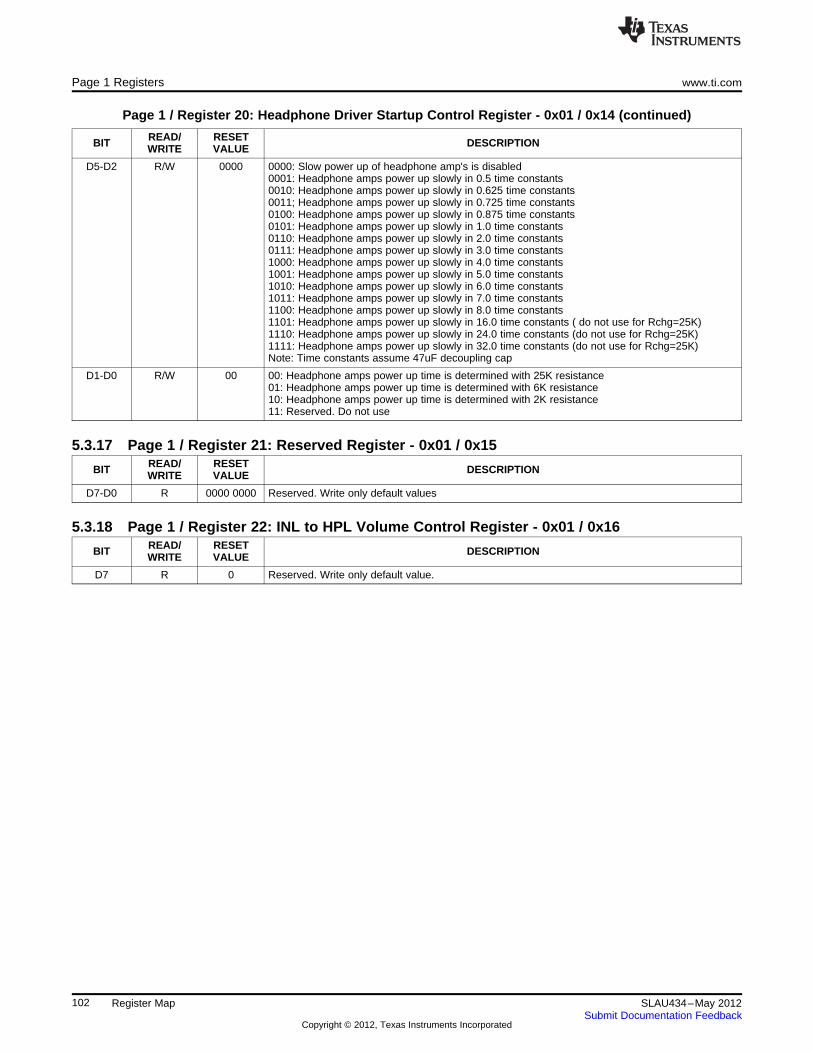
Page 1 Registers www.ti.com
Page 1 / Register 20: Headphone Driver Startup Control Register - 0x01 / 0x14 (continued)
READ/ RESETBIT DESCRIPTIONWRITE VALUE
D5-D2 R/W 0000 0000: Slow power up of headphone amp's is disabled0001: Headphone amps power up slowly in 0.5 time constants0010: Headphone amps power up slowly in 0.625 time constants0011; Headphone amps power up slowly in 0.725 time constants0100: Headphone amps power up slowly in 0.875 time constants0101: Headphone amps power up slowly in 1.0 time constants0110: Headphone amps power up slowly in 2.0 time constants0111: Headphone amps power up slowly in 3.0 time constants1000: Headphone amps power up slowly in 4.0 time constants1001: Headphone amps power up slowly in 5.0 time constants1010: Headphone amps power up slowly in 6.0 time constants1011: Headphone amps power up slowly in 7.0 time constants1100: Headphone amps power up slowly in 8.0 time constants1101: Headphone amps power up slowly in 16.0 time constants ( do not use for Rchg=25K)1110: Headphone amps power up slowly in 24.0 time constants (do not use for Rchg=25K)1111: Headphone amps power up slowly in 32.0 time constants (do not use for Rchg=25K)Note: Time constants assume 47uF decoupling cap
D1-D0 R/W 00 00: Headphone amps power up time is determined with 25K resistance01: Headphone amps power up time is determined with 6K resistance10: Headphone amps power up time is determined with 2K resistance11: Reserved. Do not use
5.3.17 Page 1 / Register 21: Reserved Register - 0x01 / 0x15READ/ RESETBIT DESCRIPTIONWRITE VALUE
D7-D0 R 0000 0000 Reserved. Write only default values
5.3.18 Page 1 / Register 22: INL to HPL Volume Control Register - 0x01 / 0x16READ/ RESETBIT DESCRIPTIONWRITE VALUE
D7 R 0 Reserved. Write only default value.
102 Register Map SLAU434–May 2012Submit Documentation Feedback
Copyright © 2012, Texas Instruments Incorporated

www.ti.com Page 1 Registers
Page 1 / Register 22: INL to HPL Volume Control Register - 0x01 / 0x16 (continued)
READ/ RESETBIT DESCRIPTIONWRITE VALUE
D6-D0 R/W 000 0000 IN1L to HPL Volume Control000 0000: Volume Control = 0.0dB000 0001: Volume Control = -0.5dB000 0010: Volume Control = -1.0dB000 0011: Volume Control = -1.5dB000 0100: Volume Control = -2.0dB000 0101: Volume Control = -2.5dB000 0110: Volume Control = -3.0dB000 0111: Volume Control = -3.5dB000 1000: Volume Control = -4.0dB000 1001: Volume Control = -4.5dB000 1010: Volume Control = -5.0dB000 1011: Volume Control = -5.5dB000 1100: Volume Control = -6.0dB000 1101: Volume Control = -7.0dB000 1110: Volume Control = -8.0dB000 1111: Volume Control = -8.5dB001 0000: Volume Control = -9.0dB001 0001: Volume Control = -9.5dB001 0010: Volume Control = -10.0dB001 0011: Volume Control = -10.5dB001 0100: Volume Control = -11.0dB001 0101: Volume Control = -11.5dB001 0110: Volume Control = -12.0dB001 0111: Volume Control = -12.5dB001 1000: Volume Control = -13.0dB001 1001: Volume Control = -13.5dB001 1010: Volume Control = -14.0dB001 1011: Volume Control = -14.5dB001 1100: Volume Control = -15.0dB001 1101: Volume Control = -15.5dB001 1110: Volume Control = -16.0dB001 1111: Volume Control = -16.5dB010 0000: Volume Control = -17.1dB010 0001: Volume Control = -17.5dB010 0010: Volume Control = -18.1dB010 0011: Volume Control = -18.6dB010 0100: Volume Control = -19.1dB010 0101: Volume Control = -19.6dB010 0110: Volume Control = -20.1dB010 0111: Volume Control = -20.6dB010 1000: Volume Control = -21.1dB010 1001: Volume Control = -21.6dB010 1010: Volume Control = -22.1dB010 1011: Volume Control = -22.6dB010 1100: Volume Control = -23.1dB010 1101: Volume Control = -23.6dB010 1110: Volume Control = -24.1dB010 1111: Volume Control = -24.6dB011 0000: Volume Control = -25.1dB011 0001: Volume Control = -25.6dB011 0010: Volume Control = -26.1dB011 0011: Volume Control = -26.6dB011 0100: Volume Control = -27.1dB011 0101: Volume Control = -27.6dB011 0110: Volume Control = -28.1dB011 0111: Volume Control = -28.6dB011 1000: Volume Control = -29.1dB011 1001: Volume Control = -29.6dB011 1010: Volume Control = -30.1dB011 1011: Volume Control = -30.6dB011 1100: Volume Control = -31.1dB011 1100: Volume Control = -31.6dB011 1101: Volume Control = -32.1dB011 1110: Volume Control = -32.6dB011 1111: Volume Control = -33.1dB100 0000: Volume Control = -33.6dB100 0001: Volume Control = -34.1dB
103SLAU434–May 2012 Register MapSubmit Documentation Feedback
Copyright © 2012, Texas Instruments Incorporated

Page 1 Registers www.ti.com
Page 1 / Register 22: INL to HPL Volume Control Register - 0x01 / 0x16 (continued)
READ/ RESETBIT DESCRIPTIONWRITE VALUE
100 0010: Volume Control = -34.6dB100 0011: Volume Control = -35.2dB100 0100: Volume Control = -35.7dB100 0101: Volume Control = -36.2dB100 0110: Volume Control = -36.7dB100 0111: Volume Control = -37.2dB100 1000: Volume Control = -37.7dB100 1001: Volume Control = -38.2dB100 1010: Volume Control = -38.7dB100 1011: Volume Control = -39.2dB100 1100: Volume Control = -39.7dB100 1101: Volume Control = -40.2dB100 1110: Volume Control = -40.7dB100 1111: Volume Control = -41.2dB101 0000: Volume Control = -41.7dB101 0001: Volume Control = -42.1dB101 0010: Volume Control = -42.7dB101 0011: Volume Control = -43.2dB101 0100: Volume Control = -43.8dB101 0101: Volume Control = -44.3dB101 0110: Volume Control = -44.8dB101 0111: Volume Control = -45.2dB101 1000: Volume Control = -45.8dB101 1001: Volume Control = -46.2dB101 1010: Volume Control = -46.7dB101 1011: Volume Control = -47.4dB101 1100: Volume Control = -47.9dB101 1101: Volume Control = -48.2dB101 1110: Volume Control = -48.7dB101 1111: Volume Control = -49.3dB110 0000: Volume Control = -50.0dB110 0001: Volume Control = -50.3dB110 0010: Volume Control = -51.0dB110 0011: Volume Control = -51.42dB110 0100: Volume Control = -51.82dB110 0101: Volume Control = -52.3dB110 0110: Volume Control = -52.7dB110 0111: Volume Control = -53.7dB110 1000: Volume Control = -54.2dB110 1001: Volume Control = -55.4dB110 1010: Volume Control = -56.7dB110 1011: Volume Control = -58.3dB110 1100: Volume Control = -60.2dB110 1101: Volume Control = -62.7dB110 1110: Volume Control = -64.3dB110 1111: Volume Control = -66.2dB111 0000: Volume Control = -68.7dB111 0001: Volume Control = -72.3dB111 0010: Volume Control = MUTE111 0011-111 1111: Reserved. Do not use
5.3.19 Page 1 / Register 23: INR to HPR Volume Control Register - 0x01 / 0x17READ/ RESETBIT DESCRIPTIONWRITE VALUE
D7 R 0 Reserved. Write only default value
104 Register Map SLAU434–May 2012Submit Documentation Feedback
Copyright © 2012, Texas Instruments Incorporated

www.ti.com Page 1 Registers
Page 1 / Register 23: INR to HPR Volume Control Register - 0x01 / 0x17 (continued)
READ/ RESETBIT DESCRIPTIONWRITE VALUE
D6-D0 R/W 000 0000 INR to HPR Volume Control000 0000: Volume Control = 0.0dB000 0001: Volume Control = -0.5dB000 0010: Volume Control = -1.0dB000 0011: Volume Control = -1.5dB000 0100: Volume Control = -2.0dB000 0101: Volume Control = -2.5dB000 0110: Volume Control = -3.0dB000 0111: Volume Control = -3.5dB000 1000: Volume Control = -4.0dB000 1001: Volume Control = -4.5dB000 1010: Volume Control = -5.0dB000 1011: Volume Control = -5.5dB000 1100: Volume Control = -6.0dB000 1101: Volume Control = -7.0dB000 1110: Volume Control = -8.0dB000 1111: Volume Control = -8.5dB001 0000: Volume Control = -9.0dB001 0001: Volume Control = -9.5dB001 0010: Volume Control = -10.0dB001 0011: Volume Control = -10.5dB001 0100: Volume Control = -11.0dB001 0101: Volume Control = -11.5dB001 0110: Volume Control = -12.0dB001 0111: Volume Control = -12.5dB001 1000: Volume Control = -13.0dB001 1001: Volume Control = -13.5dB001 1010: Volume Control = -14.0dB001 1011: Volume Control = -14.5dB001 1100: Volume Control = -15.0dB001 1101: Volume Control = -15.5dB001 1110: Volume Control = -16.0dB001 1111: Volume Control = -16.5dB010 0000: Volume Control = -17.1dB010 0001: Volume Control = -17.5dB010 0010: Volume Control = -18.1dB010 0011: Volume Control = -18.6dB010 0100: Volume Control = -19.1dB010 0101: Volume Control = -19.6dB010 0110: Volume Control = -20.1dB010 0111: Volume Control = -20.6dB010 1000: Volume Control = -21.1dB010 1001: Volume Control = -21.6dB010 1010: Volume Control = -22.1dB010 1011: Volume Control = -22.6dB010 1100: Volume Control = -23.1dB010 1101: Volume Control = -23.6dB010 1110: Volume Control = -24.1dB010 1111: Volume Control = -24.6dB011 0000: Volume Control = -25.1dB011 0001: Volume Control = -25.6dB011 0010: Volume Control = -26.1dB011 0011: Volume Control = -26.6dB011 0100: Volume Control = -27.1dB011 0101: Volume Control = -27.6dB011 0110: Volume Control = -28.1dB011 0111: Volume Control = -28.6dB011 1000: Volume Control = -29.1dB011 1001: Volume Control = -29.6dB011 1010: Volume Control = -30.1dB011 1011: Volume Control = -30.6dB011 1100: Volume Control = -31.1dB011 1100: Volume Control = -31.6dB011 1101: Volume Control = -32.1dB011 1110: Volume Control = -32.6dB011 1111: Volume Control = -33.1dB100 0000: Volume Control = -33.6dB100 0001: Volume Control = -34.1dB
105SLAU434–May 2012 Register MapSubmit Documentation Feedback
Copyright © 2012, Texas Instruments Incorporated

Page 1 Registers www.ti.com
Page 1 / Register 23: INR to HPR Volume Control Register - 0x01 / 0x17 (continued)
READ/ RESETBIT DESCRIPTIONWRITE VALUE
100 0010: Volume Control = -34.6dB100 0011: Volume Control = -35.2dB100 0100: Volume Control = -35.7dB100 0101: Volume Control = -36.2dB100 0110: Volume Control = -36.7dB100 0111: Volume Control = -37.2dB100 1000: Volume Control = -37.7dB100 1001: Volume Control = -38.2dB100 1010: Volume Control = -38.7dB100 1011: Volume Control = -39.2dB100 1100: Volume Control = -39.7dB100 1101: Volume Control = -40.2dB100 1110: Volume Control = -40.7dB100 1111: Volume Control = -41.2dB101 0000: Volume Control = -41.7dB101 0001: Volume Control = -42.1dB101 0010: Volume Control = -42.7dB101 0011: Volume Control = -43.2dB101 0100: Volume Control = -43.8dB101 0101: Volume Control = -44.3dB101 0110: Volume Control = -44.8dB101 0111: Volume Control = -45.2dB101 1000: Volume Control = -45.8dB101 1001: Volume Control = -46.2dB101 1010: Volume Control = -46.7dB101 1011: Volume Control = -47.4dB101 1100: Volume Control = -47.9dB101 1101: Volume Control = -48.2dB101 1110: Volume Control = -48.7dB101 1111: Volume Control = -49.3dB110 0000: Volume Control = -50.0dB110 0001: Volume Control = -50.3dB110 0010: Volume Control = -51.0dB110 0011: Volume Control = -51.42dB110 0100: Volume Control = -51.82dB110 0101: Volume Control = -52.3dB110 0110: Volume Control = -52.7dB110 0111: Volume Control = -53.7dB110 1000: Volume Control = -54.2dB110 1001: Volume Control = -55.4dB110 1010: Volume Control = -56.7dB110 1011: Volume Control = -58.3dB110 1100: Volume Control = -60.2dB110 1101: Volume Control = -62.7dB110 1110: Volume Control = -64.3dB110 1111: Volume Control = -66.2dB111 0000: Volume Control = -68.7dB111 0001: Volume Control = -72.3dB111 0010: Volume Control = MUTE111 0011-111 1111: Reserved. Do not use
5.3.20 Page 1 / Register 24-50: Reserved Register - 0x01 / 0x18-0x32READ/ RESETBIT DESCRIPTIONWRITE VALUE
D7-D0 R 0000 0000 Reserved. Write only default values
5.3.21 Page 1 / Register 51: MICBIAS Configuration Register - 0x01 / 0x33READ/ RESETBIT DESCRIPTIONWRITE VALUE
D7 R 0 Reserved. Write only default value.
D6 R/W 0 0: MICBIAS powered down1: MICBIAS powered up
106 Register Map SLAU434–May 2012Submit Documentation Feedback
Copyright © 2012, Texas Instruments Incorporated

www.ti.com Page 1 Registers
Page 1 / Register 51: MICBIAS Configuration Register - 0x01 / 0x33 (continued)
READ/ RESETBIT DESCRIPTIONWRITE VALUE
D5-D4 R/W 00 MICBIAS Output Voltage Configuration00: MICBIAS = 1.04V (CM=0.75V) or MICBIAS = 1.25V(CM=0.9V)01: MICBIAS = 1.425V(CM=0.75V) or MICBIAS = 1.7V(CM=0.9V)10: MICBIAS = 2.075V(CM=0.75V) or MICBIAS = 2.5V(CM=0.9V)11: MICBIAS is switch to power supply
D3 R/W 0 0: MICBIAS voltage is generated from AVDD1: MICBIAS voltage is generated from LDOIN
D2-D0 R 000 Reserved. Write only default value.
5.3.22 Page 1 / Register 52-57: Reserved Register - 0x01 / 0x34-0x39READ/ RESETBIT DESCRIPTIONWRITE VALUE
D7-D0 R 0000 0000 Reserved. Write only default values
5.3.23 Page 1 / Register 58: Analog Input Settings - 0x01 / 0x3AREAD/ RESETBIT DESCRIPTIONWRITE VALUE
D7 R/W 0 Not routed INL settings0: INL is floated if not routed to HPL1: INL is connected to CM if not routed to HPL
D6 R/W 0 Not routed INR settings0: INR is floated if not routed to HPR1: INR is connected to CM if not routed to HPR
D5-D0 R 00 0000 Reserved. Write only default value.
5.3.24 Page 1 / Register 59-62: Reserved Register - 0x01 / 0x3B-0x3EREAD/ RESETBIT DESCRIPTIONWRITE VALUE
D7-D0 R 1000 0000 Reserved. Write only default values
5.3.25 Page 1 / Register 63: DAC Analog Gain Control Flag Register - 0x01 / 0x3FREAD/ RESETBIT DESCRIPTIONWRITE VALUE
D7 R 0 HPL Gain Flag0: Applied Gain is not equal to Programmed Gain1: Applied Gain is equal to Programmed Gain
D6 R 0 HPR Gain Flag0: Applied Gain is not equal to Programmed Gain1: Applied Gain is equal to Programmed Gain
D5-D4 R 00 Reserved. Write only default values
D3 R 0 IN1L to HPL Bypass Volume Flag0: Applied Volume is not equal to Programmed Volume1: Applied Volume is equal to Programmed Volume
D2 R 0 IN1R to HPR Bypass Volume Flag0: Applied Volume is not equal to Programmed Volume1: Applied Volume is equal to Programmed Volume
D1-D0 R 00 Reserved. Write only default values
5.3.26 Page 1 / Register 64-70: Reserved Register - 0x01 / 0x40-0x46READ/ RESETBIT DESCRIPTIONWRITE VALUE
D7-D0 R 0000 0000 Reserved. Write only default values
107SLAU434–May 2012 Register MapSubmit Documentation Feedback
Copyright © 2012, Texas Instruments Incorporated

Page 1 Registers www.ti.com
5.3.27 Page 1 / Register 71: Analog Input Quick Charging Configuration Register - 0x01 / 0x47READ/ RESETBIT DESCRIPTIONWRITE VALUE
D7-D6 R 00 Reserved. Write only default values
D5-D0 R/W 00 0000 Analog inputs power up time00 0000: Default. Use one of the values give below11 0001: Analog inputs power up time is 3.1 ms11 0010: Analog inputs power up time is 6.4 ms11 0011: Analog inputs power up time is 1.6 msOthers: Do not use
5.3.28 Page 1 / Register 72-122: Reserved Register - 0x01 / 0x48-0x7AREAD/ RESETBIT DESCRIPTIONWRITE VALUE
D7-D0 R 0000 0000 Reserved. Write only default values
5.3.29 Page 1 / Register 123: Reference Power-up Configuration Register - 0x01 / 0x7BREAD/ RESETBIT DESCRIPTIONWRITE VALUE
D7-D3 R 0 0000 Reserved. Write only default values
D2-D0 R/W 000 Reference Power Up configuration000: Reference will power up slowly when analog blocks are powered up001: Reference will power up in 40ms when analog blocks are powered up010: Reference will power up in 80ms when analog blocks are powered up011: Reference will power up in 120ms when analog blocks are powered up100: Force power up of reference. Power up will be slow101: Force power up of reference. Power up time will be 40ms110: Force power up of reference. Power up time will be 80ms111: Force power up of reference. Power up time will be 120ms
5.3.30 Page 1 / Register 124: Reserved Register - 0x01 / 0x7CREAD/ RESETBIT DESCRIPTIONWRITE VALUE
D7-D0 R 0000 0000 Reserved. Write only default values
5.3.31 Page 1 / Register 125: Offset Callibration Register - 0x01 / 0x7DREAD/ RESETBIT DESCRIPTIONWRITE VALUE
D7-D5 R 000 Offset correction Clock Divider000: Offset correction takes 190*197 oscillator clock cycles001: Offset correction takes 38*197 oscillator clock cycles010: Offset correction takes 76*197 oscillator clock cycles011: Offset correction takes 114*197 oscillator clock cycles100: Offset correction takes 142*197 oscillator clock cycles101: Offset correction takes 190*197 oscillator clock cycles110: Offset correction takes 228*197 oscillator clock cycles111: Offset correction takes 266*197 oscillator clock cycles
D4-D2 R 0 00 Reserved. Write only default values
D1-D0 R/W 00 Offset correction settings00: Offset correction disabled01: Force calibrate for offset at Headphone Power-up for routings selected10: Callibrate for offset at headphone power-up for selected routings only for first power-up ofheadphone11: Do not use
5.3.32 Page 1 / Register 126-127: Reserved Register - 0x01 / 0x7E-0x7FREAD/ RESETBIT DESCRIPTIONWRITE VALUE
D7-D0 R 0000 0000 Reserved. Write only default values
108 Register Map SLAU434–May 2012Submit Documentation Feedback
Copyright © 2012, Texas Instruments Incorporated
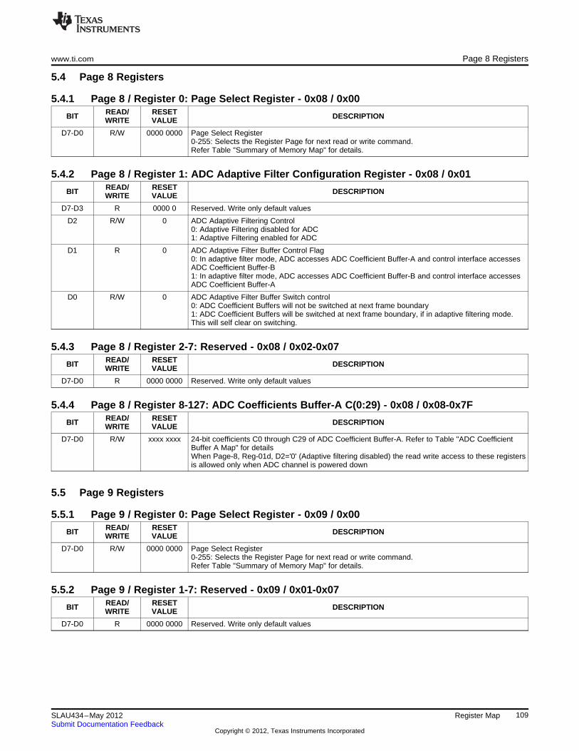
www.ti.com Page 8 Registers
5.4 Page 8 Registers
5.4.1 Page 8 / Register 0: Page Select Register - 0x08 / 0x00READ/ RESETBIT DESCRIPTIONWRITE VALUE
D7-D0 R/W 0000 0000 Page Select Register0-255: Selects the Register Page for next read or write command.Refer Table "Summary of Memory Map" for details.
5.4.2 Page 8 / Register 1: ADC Adaptive Filter Configuration Register - 0x08 / 0x01READ/ RESETBIT DESCRIPTIONWRITE VALUE
D7-D3 R 0000 0 Reserved. Write only default values
D2 R/W 0 ADC Adaptive Filtering Control0: Adaptive Filtering disabled for ADC1: Adaptive Filtering enabled for ADC
D1 R 0 ADC Adaptive Filter Buffer Control Flag0: In adaptive filter mode, ADC accesses ADC Coefficient Buffer-A and control interface accessesADC Coefficient Buffer-B1: In adaptive filter mode, ADC accesses ADC Coefficient Buffer-B and control interface accessesADC Coefficient Buffer-A
D0 R/W 0 ADC Adaptive Filter Buffer Switch control0: ADC Coefficient Buffers will not be switched at next frame boundary1: ADC Coefficient Buffers will be switched at next frame boundary, if in adaptive filtering mode.This will self clear on switching.
5.4.3 Page 8 / Register 2-7: Reserved - 0x08 / 0x02-0x07READ/ RESETBIT DESCRIPTIONWRITE VALUE
D7-D0 R 0000 0000 Reserved. Write only default values
5.4.4 Page 8 / Register 8-127: ADC Coefficients Buffer-A C(0:29) - 0x08 / 0x08-0x7FREAD/ RESETBIT DESCRIPTIONWRITE VALUE
D7-D0 R/W xxxx xxxx 24-bit coefficients C0 through C29 of ADC Coefficient Buffer-A. Refer to Table "ADC CoefficientBuffer A Map" for detailsWhen Page-8, Reg-01d, D2='0' (Adaptive filtering disabled) the read write access to these registersis allowed only when ADC channel is powered down
5.5 Page 9 Registers
5.5.1 Page 9 / Register 0: Page Select Register - 0x09 / 0x00READ/ RESETBIT DESCRIPTIONWRITE VALUE
D7-D0 R/W 0000 0000 Page Select Register0-255: Selects the Register Page for next read or write command.Refer Table "Summary of Memory Map" for details.
5.5.2 Page 9 / Register 1-7: Reserved - 0x09 / 0x01-0x07READ/ RESETBIT DESCRIPTIONWRITE VALUE
D7-D0 R 0000 0000 Reserved. Write only default values
109SLAU434–May 2012 Register MapSubmit Documentation Feedback
Copyright © 2012, Texas Instruments Incorporated
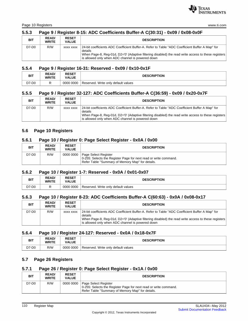
Page 10 Registers www.ti.com
5.5.3 Page 9 / Register 8-15: ADC Coefficients Buffer-A C(30:31) - 0x09 / 0x08-0x0FREAD/ RESETBIT DESCRIPTIONWRITE VALUE
D7-D0 R/W xxxx xxxx 24-bit coefficients ADC Coefficient Buffer-A. Refer to Table "ADC Coefficient Buffer A Map" fordetailsWhen Page-8, Reg-01d, D2='0' (Adaptive filtering disabled) the read write access to these registersis allowed only when ADC channel is powered down
5.5.4 Page 9 / Register 16-31: Reserved - 0x09 / 0x10-0x1FREAD/ RESETBIT DESCRIPTIONWRITE VALUE
D7-D0 R 0000 0000 Reserved. Write only default values
5.5.5 Page 9 / Register 32-127: ADC Coefficients Buffer-A C(36:59) - 0x09 / 0x20-0x7FREAD/ RESETBIT DESCRIPTIONWRITE VALUE
D7-D0 R/W xxxx xxxx 24-bit coefficients ADC Coefficient Buffer-A. Refer to Table "ADC Coefficient Buffer A Map" fordetailsWhen Page-8, Reg-01d, D2='0' (Adaptive filtering disabled) the read write access to these registersis allowed only when ADC channel is powered down
5.6 Page 10 Registers
5.6.1 Page 10 / Register 0: Page Select Register - 0x0A / 0x00READ/ RESETBIT DESCRIPTIONWRITE VALUE
D7-D0 R/W 0000 0000 Page Select Register0-255: Selects the Register Page for next read or write command.Refer Table "Summary of Memory Map" for details.
5.6.2 Page 10 / Register 1-7: Reserved - 0x0A / 0x01-0x07READ/ RESETBIT DESCRIPTIONWRITE VALUE
D7-D0 R 0000 0000 Reserved. Write only default values
5.6.3 Page 10 / Register 8-23: ADC Coefficients Buffer-A C(60:63) - 0x0A / 0x08-0x17READ/ RESETBIT DESCRIPTIONWRITE VALUE
D7-D0 R/W xxxx xxxx 24-bit coefficients ADC Coefficient Buffer-A. Refer to Table "ADC Coefficient Buffer A Map" fordetailsWhen Page-8, Reg-01d, D2='0' (Adaptive filtering disabled) the read write access to these registersis allowed only when ADC channel is powered down
5.6.4 Page 10 / Register 24-127: Reserved - 0x0A / 0x18-0x7FREAD/ RESETBIT DESCRIPTIONWRITE VALUE
D7-D0 R/W 0000 0000 Reserved. Write only default values
5.7 Page 26 Registers
5.7.1 Page 26 / Register 0: Page Select Register - 0x1A / 0x00READ/ RESETBIT DESCRIPTIONWRITE VALUE
D7-D0 R/W 0000 0000 Page Select Register0-255: Selects the Register Page for next read or write command.Refer Table "Summary of Memory Map" for details.
110 Register Map SLAU434–May 2012Submit Documentation Feedback
Copyright © 2012, Texas Instruments Incorporated
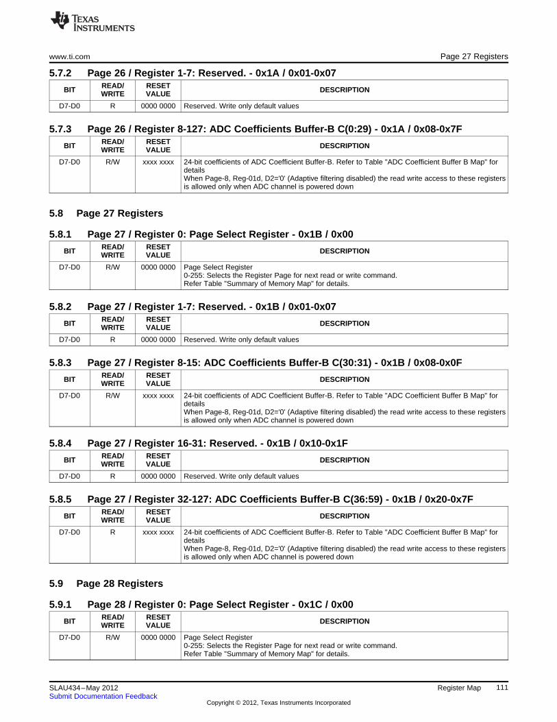
www.ti.com Page 27 Registers
5.7.2 Page 26 / Register 1-7: Reserved. - 0x1A / 0x01-0x07READ/ RESETBIT DESCRIPTIONWRITE VALUE
D7-D0 R 0000 0000 Reserved. Write only default values
5.7.3 Page 26 / Register 8-127: ADC Coefficients Buffer-B C(0:29) - 0x1A / 0x08-0x7FREAD/ RESETBIT DESCRIPTIONWRITE VALUE
D7-D0 R/W xxxx xxxx 24-bit coefficients of ADC Coefficient Buffer-B. Refer to Table "ADC Coefficient Buffer B Map" fordetailsWhen Page-8, Reg-01d, D2='0' (Adaptive filtering disabled) the read write access to these registersis allowed only when ADC channel is powered down
5.8 Page 27 Registers
5.8.1 Page 27 / Register 0: Page Select Register - 0x1B / 0x00READ/ RESETBIT DESCRIPTIONWRITE VALUE
D7-D0 R/W 0000 0000 Page Select Register0-255: Selects the Register Page for next read or write command.Refer Table "Summary of Memory Map" for details.
5.8.2 Page 27 / Register 1-7: Reserved. - 0x1B / 0x01-0x07READ/ RESETBIT DESCRIPTIONWRITE VALUE
D7-D0 R 0000 0000 Reserved. Write only default values
5.8.3 Page 27 / Register 8-15: ADC Coefficients Buffer-B C(30:31) - 0x1B / 0x08-0x0FREAD/ RESETBIT DESCRIPTIONWRITE VALUE
D7-D0 R/W xxxx xxxx 24-bit coefficients of ADC Coefficient Buffer-B. Refer to Table "ADC Coefficient Buffer B Map" fordetailsWhen Page-8, Reg-01d, D2='0' (Adaptive filtering disabled) the read write access to these registersis allowed only when ADC channel is powered down
5.8.4 Page 27 / Register 16-31: Reserved. - 0x1B / 0x10-0x1FREAD/ RESETBIT DESCRIPTIONWRITE VALUE
D7-D0 R 0000 0000 Reserved. Write only default values
5.8.5 Page 27 / Register 32-127: ADC Coefficients Buffer-B C(36:59) - 0x1B / 0x20-0x7FREAD/ RESETBIT DESCRIPTIONWRITE VALUE
D7-D0 R xxxx xxxx 24-bit coefficients of ADC Coefficient Buffer-B. Refer to Table "ADC Coefficient Buffer B Map" fordetailsWhen Page-8, Reg-01d, D2='0' (Adaptive filtering disabled) the read write access to these registersis allowed only when ADC channel is powered down
5.9 Page 28 Registers
5.9.1 Page 28 / Register 0: Page Select Register - 0x1C / 0x00READ/ RESETBIT DESCRIPTIONWRITE VALUE
D7-D0 R/W 0000 0000 Page Select Register0-255: Selects the Register Page for next read or write command.Refer Table "Summary of Memory Map" for details.
111SLAU434–May 2012 Register MapSubmit Documentation Feedback
Copyright © 2012, Texas Instruments Incorporated

Page 44 Registers www.ti.com
5.9.2 Page 28 / Register 1-7: Reserved. - 0x1C / 0x01-0x07READ/ RESETBIT DESCRIPTIONWRITE VALUE
D7-D0 R 0000 0000 Reserved. Write only default values
5.9.3 Page 28 / Register 8-23: ADC Coefficients Buffer-B C(60:63) - 0x1C / 0x08-0x17READ/ RESETBIT DESCRIPTIONWRITE VALUE
D7-D0 R/W xxxx xxxx 24-bit coefficients of ADC Coefficient Buffer-B. Refer to Table "ADC Coefficient Buffer B Map" fordetailsWhen Page-8, Reg-01d, D2='0' (Adaptive filtering disabled) the read write access to these registersis allowed only when ADC channel is powered down
5.9.4 Page 28 / Register 24-127: Reserved. - 0x1C / 0x18-0x7FREAD/ RESETBIT DESCRIPTIONWRITE VALUE
D7-D0 R 0000 0000 Reserved. Write only default values
5.10 Page 44 Registers
5.10.1 Page 44 / Register 0: Page Select Register - 0x2C / 0x00READ/ RESETBIT DESCRIPTIONWRITE VALUE
D7-D0 R/W 0000 0000 Page Select Register0-255: Selects the Register Page for next read or write command.Refer Table "Summary of Memory Map" for details.
5.10.2 Page 44 / Register 1: DAC Adaptive Filter Configuration Register - 0x2C / 0x01READ/ RESETBIT DESCRIPTIONWRITE VALUE
D7-D3 R 0000 0 Reserved. Write only default values
D2 R/W 0 DAC Adaptive Filtering Control0: Adaptive Filtering disabled for DAC1: Adaptive Filtering enabled for DAC
D1 R 0 DAC Adaptive Filter Buffer Control Flag0: In adaptive filter mode, DAC accesses DAC Coefficient Buffer-A and control interface accessesDAC Coefficient Buffer-B1: In adaptive filter mode, DAC accesses DAC Coefficient Buffer-B and control interface accessesDAC Coefficient Buffer-A
D0 R/W 0 DAC Adaptive Filter Buffer Switch control0: DAC Coefficient Buffers will not be switched at next frame boundary1: DAC Coefficient Buffers will be switched at next frame boundary, if in adaptive filtering mode.This will self clear on switching.
5.10.3 Page 44 / Register 2-7: Reserved - 0x2C / 0x02-0x07READ/ RESETBIT DESCRIPTIONWRITE VALUE
D7-D0 R 0000 0000 Reserved. Write only default values
5.10.4 Page 44 / Register 8-11: DAC Coefficients Buffer-A C(0:29) - 0x2C / 0x08-0x0BREAD/ RESETBIT DESCRIPTIONWRITE VALUE
D7-D0 R/W xxxx xxxx 24-bit coefficients C0 through C29 of DAC Coefficient Buffer-A. Refer to Table "DAC CoefficientBuffer A Map" for detailsWhen Page-44, Reg-01d, D2='0' (Adaptive filtering disabled) the read write access to theseregisters is allowed only when DAC channel is powered down
112 Register Map SLAU434–May 2012Submit Documentation Feedback
Copyright © 2012, Texas Instruments Incorporated
www.ti.com Page 45 Registers
5.11 Page 45 Registers
5.11.1 Page 45 / Register 0: Page Select Register - 0x2D / 0x00READ/ RESETBIT DESCRIPTIONWRITE VALUE
D7-D0 R/W 0000 0000 Page Select Register0-255: Selects the Register Page for next read or write command.Refer Table "Summary of Memory Map" for details.
5.11.2 Page 45 / Register 1-7: Reserved - 0x2D / 0x01-0x07READ/ RESETBIT DESCRIPTIONWRITE VALUE
D7-D0 R 0000 0000 Reserved. Write only default values
5.11.3 Page 45 / Register 8-11: DAC Coefficients Buffer-A C(30) - 0x2D / 0x08-0x0BREAD/ RESETBIT DESCRIPTIONWRITE VALUE
D7-D0 R/W xxxx xxxx 24-bit coefficients DAC Coefficient Buffer-A. Refer to Table "DAC Coefficient Buffer A Map" fordetailsWhen Page-44, Reg-01d, D2='0' (Adaptive filtering disabled) the read write access to theseregisters is allowed only when DAC channel is powered down
5.11.4 Page 45 / Register 12-15: Reserved - 0x2D / 0x0C-0x0FREAD/ RESETBIT DESCRIPTIONWRITE VALUE
D7-D0 R 0000 0000 Reserved. Write only default values
5.11.5 Page 45 / Register 16-127: DAC Coefficients Buffer-A C(32:59) - 0x2D / 0x10-0x7FREAD/ RESETBIT DESCRIPTIONWRITE VALUE
D7-D0 R/W xxxx xxxx 24-bit coefficients DAC Coefficient Buffer-A. Refer to Table "DAC Coefficient Buffer A Map" fordetailsWhen Page-44, Reg-01d, D2='0' (Adaptive filtering disabled) the read write access to theseregisters is allowed only when DAC channel is powered down
5.12 Page 46 Registers
5.12.1 Page 46 / Register 0: Page Select Register - 0x2E / 0x00READ/ RESETBIT DESCRIPTIONWRITE VALUE
D7-D0 R/W 0000 0000 Page Select Register0-255: Selects the Register Page for next read or write command.Refer Table "Summary of Memory Map" for details.
5.12.2 Page 46 / Register 1-7: Reserved - 0x2E / 0x01-0x07READ/ RESETBIT DESCRIPTIONWRITE VALUE
D7-D0 R 0000 0000 Reserved. Write only default values
5.12.3 Page 46 / Register 8-19: DAC Coefficients Buffer-A C(60:62) - 0x2E / 0x08-0x13READ/ RESETBIT DESCRIPTIONWRITE VALUE
D7-D0 R/W xxxx xxxx 24-bit coefficients DAC Coefficient Buffer-A. Refer to Table "DAC Coefficient Buffer A Map" fordetailsWhen Page-44, Reg-01d, D2='0' (Adaptive filtering disabled) the read write access to theseregisters is allowed only when DAC channel is powered down
113SLAU434–May 2012 Register MapSubmit Documentation Feedback
Copyright © 2012, Texas Instruments Incorporated
Page 62 Registers www.ti.com
5.12.4 Page 46 / Register 20-27: Reserved - 0x2E / 0x14-0x1BREAD/ RESETBIT DESCRIPTIONWRITE VALUE
D7-D0 R 0000 0000 Reserved. Write only default values
5.12.5 Page 46 / Register 28-75: DAC Coefficients Buffer-A C(65:76) - 0x2E / 0x1C-0x4BREAD/ RESETBIT DESCRIPTIONWRITE VALUE
D7-D0 R 0000 0000 24-bit coefficients DAC Coefficient Buffer-A. Refer to Table "DAC Coefficient Buffer A Map" fordetailsWhen Page-44, Reg-01d, D2='0' (Adaptive filtering disabled) the read write access to theseregisters is allowed only when DAC channel is powered down
5.12.6 Page 46 / Register 76-127: Reserved - 0x2E / 0x4C-0x7FREAD/ RESETBIT DESCRIPTIONWRITE VALUE
D7-D0 R 0000 0000 Reserved. Write only default values
5.13 Page 62 Registers
5.13.1 Page 62 / Register 0: Page Select Register - 0x3E / 0x00READ/ RESETBIT DESCRIPTIONWRITE VALUE
D7-D0 R/W 0000 0000 Page Select Register0-255: Selects the Register Page for next read or write command.Refer Table "Summary of Memory Map" for details.
5.13.2 Page 62 / Register 1-7: Reserved. - 0x3E / 0x01-0x07READ/ RESETBIT DESCRIPTIONWRITE VALUE
D7-D0 R 0000 0000 Reserved. Write only default values
5.13.3 Page 62 / Register 8-127: DAC Coefficients Buffer-B C(0:29) - 0x3E / 0x08-0x7FREAD/ RESETBIT DESCRIPTIONWRITE VALUE
D7-D0 R/W xxxx xxxx 24-bit coefficients of DAC Coefficient Buffer-B. Refer Table "DAC Coefficient Buffer B Map" fordetailsWhen Page-44, Reg-01d, D2='0' (Adaptive filtering disabled) the read write access to theseregisters is allowed only when DAC channel is powered down
5.14 Page 63 Registers
5.14.1 Page 63 / Register 0: Page Select Register - 0x3F / 0x00READ/ RESETBIT DESCRIPTIONWRITE VALUE
D7-D0 R/W 0000 0000 Page Select Register0-255: Selects the Register Page for next read or write command.Refer Table "Summary of Memory Map" for details.
5.14.2 Page 63 / Register 1-7: Reserved. - 0x3F / 0x01-0x07READ/ RESETBIT DESCRIPTIONWRITE VALUE
D7-D0 R 0000 0000 Reserved. Write only default values
114 Register Map SLAU434–May 2012Submit Documentation Feedback
Copyright © 2012, Texas Instruments Incorporated

www.ti.com Page 63 Registers
5.14.3 Page 63 / Register 8-11: DAC Coefficients Buffer-B C(30) - 0x3F / 0x08-0x0BREAD/ RESETBIT DESCRIPTIONWRITE VALUE
D7-D0 R/W xxxx xxxx 24-bit coefficients of DAC Coefficient Buffer-B. Refer Table "DAC Coefficient Buffer B Map" fordetailsWhen Page-44, Reg-01d, D2='0' (Adaptive filtering disabled) the read write access to theseregisters is allowed only when DAC channel is powered down
5.14.4 Page 63 / Register 12-15: Reserved. - 0x3F / 0x0C-0x0FREAD/ RESETBIT DESCRIPTIONWRITE VALUE
D7-D0 R 0000 0000 Reserved. Write only default values
5.14.5 Page 63 / Register 16-127: DAC Coefficients Buffer-B C(32:59) - 0x3F / 0x10-0x7FREAD/ RESETBIT DESCRIPTIONWRITE VALUE
D7-D0 R 0000 0000 24-bit coefficients of DAC Coefficient Buffer-B. Refer Table "DAC Coefficient Buffer B Map" fordetailsWhen Page-44, Reg-01d, D2='0' (Adaptive filtering disabled) the read write access to theseregisters is allowed only when DAC channel is powered down
5.15 Page 63 Registers
5.15.1 Page 63 / Register 0: Page Select Register - 0x3F / 0x00READ/ RESETBIT DESCRIPTIONWRITE VALUE
D7-D0 R/W 0000 0000 Page Select Register0-255: Selects the Register Page for next read or write command.Refer Table "Summary of Memory Map" for details.
5.15.2 Page 63 / Register 1-7: Reserved - 0x3F / 0x01-0x07READ/ RESETBIT DESCRIPTIONWRITE VALUE
D7-D0 R 0000 0000 Reserved. Write only default values
5.15.3 Page 63 / Register 8-19: DAC Coefficients Buffer-B C(60:62) - 0x3F / 0x08-0x13READ/ RESETBIT DESCRIPTIONWRITE VALUE
D7-D0 R/W xxxx xxxx 24-bit coefficients of DAC Coefficient Buffer-B. Refer Table "DAC Coefficient Buffer B Map" fordetailsWhen Page-44, Reg-01d, D2='0' (Adaptive filtering disabled) the read write access to theseregisters is allowed only when DAC channel is powered down
5.15.4 Page 63 / Register 20-27: Reserved - 0x3F / 0x14-0x1BREAD/ RESETBIT DESCRIPTIONWRITE VALUE
D7-D0 R 0000 0000 Reserved. Write only default values
5.15.5 Page 63 / Register 28-75: DAC Coefficients Buffer-B C(65:76) - 0x3F / 0x1C-0x4BREAD/ RESETBIT DESCRIPTIONWRITE VALUE
D7-D0 R 0000 0000 24-bit coefficients of DAC Coefficient Buffer-B. Refer Table "DAC Coefficient Buffer B Map" fordetailsWhen Page-44, Reg-01d, D2='0' (Adaptive filtering disabled) the read write access to theseregisters is allowed only when DAC channel is powered down
115SLAU434–May 2012 Register MapSubmit Documentation Feedback
Copyright © 2012, Texas Instruments Incorporated
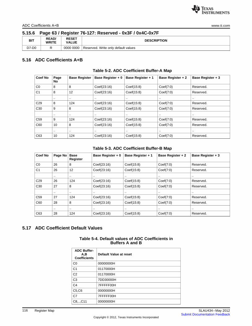
ADC Coefficients A+B www.ti.com
5.15.6 Page 63 / Register 76-127: Reserved - 0x3F / 0x4C-0x7FREAD/ RESETBIT DESCRIPTIONWRITE VALUE
D7-D0 R 0000 0000 Reserved. Write only default values
5.16 ADC Coefficients A+B
Table 5-2. ADC Coefficient Buffer-A Map
Coef No Page Base Register Base Register + 0 Base Register + 1 Base Register + 2 Base Register + 3No
C0 8 8 Coef(23:16) Coef(15:8) Coef(7:0) Reserved.
C1 8 12 Coef(23:16) Coef(15:8) Coef(7:0) Reserved.
.. .. .. .. .. ..
C29 8 124 Coef(23:16) Coef(15:8) Coef(7:0) Reserved.
C30 9 8 Coef(23:16) Coef(15:8) Coef(7:0) Reserved.
.. .. .. .. .. ..
C59 9 124 Coef(23:16) Coef(15:8) Coef(7:0) Reserved.
C60 10 8 Coef(23:16) Coef(15:8) Coef(7:0) Reserved.
.. .. .. .. .. ..
C63 10 124 Coef(23:16) Coef(15:8) Coef(7:0) Reserved.
Table 5-3. ADC Coefficient Buffer-B Map
Coef No Page No Base Base Register + 0 Base Register + 1 Base Register + 2 Base Register + 3Register
C0 26 8 Coef(23:16) Coef(15:8) Coef(7:0) Reserved.
C1 26 12 Coef(23:16) Coef(15:8) Coef(7:0) Reserved.
.. .. .. .. .. ..
C29 26 124 Coef(23:16) Coef(15:8) Coef(7:0) Reserved.
C30 27 8 Coef(23:16) Coef(15:8) Coef(7:0) Reserved.
.. .. .. .. .. ..
C59 27 124 Coef(23:16) Coef(15:8) Coef(7:0) Reserved.
C60 28 8 Coef(23:16) Coef(15:8) Coef(7:0) Reserved.
.. .. .. .. .. ..
C63 28 124 Coef(23:16) Coef(15:8) Coef(7:0) Reserved.
5.17 ADC Coefficient Default Values
Table 5-4. Default values of ADC Coefficients inBuffers A and B
ADC Buffer-A,B Default Value at reset
Coefficients
C0 00000000H
C1 01170000H
C2 01170000H
C3 7DD30000H
C4 7FFFFF00H
C5,C6 00000000H
C7 7FFFFF00H
C8,..,C11 00000000H
116 Register Map SLAU434–May 2012Submit Documentation Feedback
Copyright © 2012, Texas Instruments Incorporated
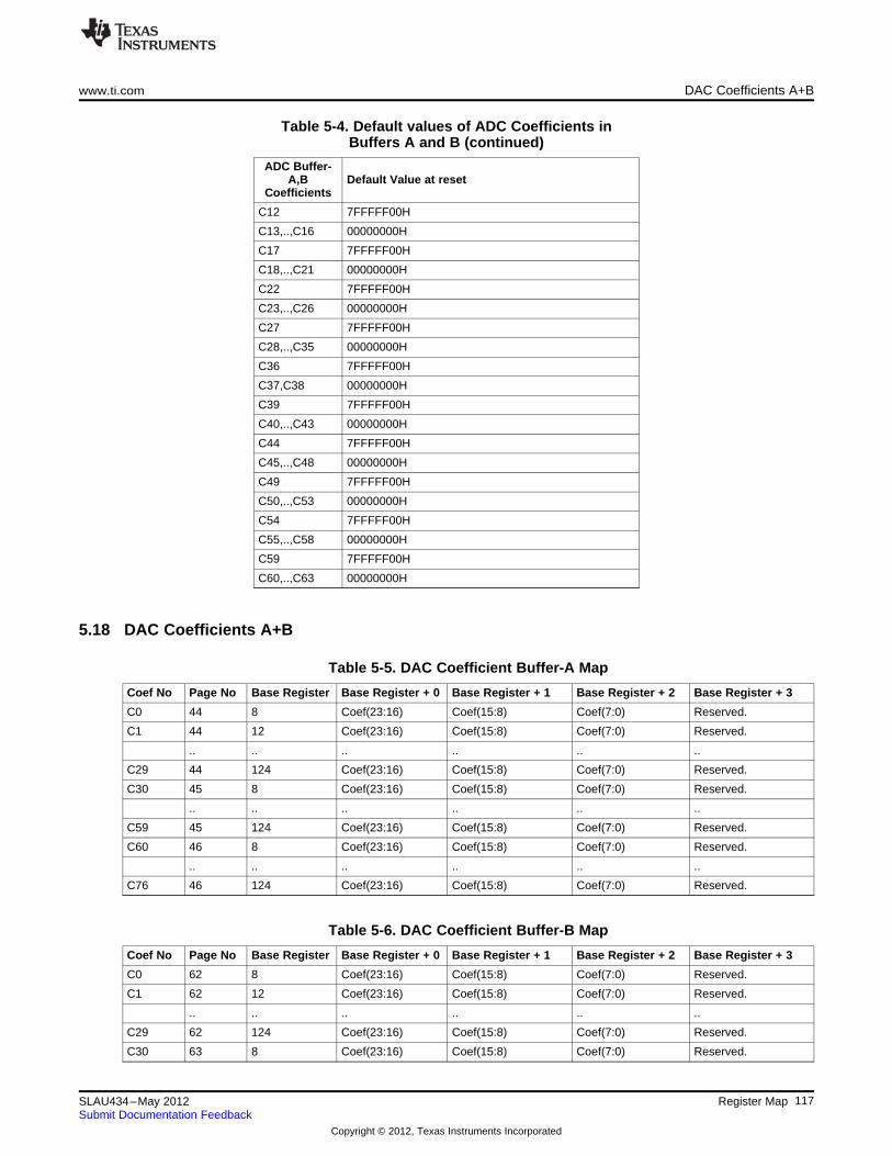
www.ti.com DAC Coefficients A+B
Table 5-4. Default values of ADC Coefficients inBuffers A and B (continued)
ADC Buffer-A,B Default Value at reset
Coefficients
C12 7FFFFF00H
C13,..,C16 00000000H
C17 7FFFFF00H
C18,..,C21 00000000H
C22 7FFFFF00H
C23,..,C26 00000000H
C27 7FFFFF00H
C28,..,C35 00000000H
C36 7FFFFF00H
C37,C38 00000000H
C39 7FFFFF00H
C40,..,C43 00000000H
C44 7FFFFF00H
C45,..,C48 00000000H
C49 7FFFFF00H
C50,..,C53 00000000H
C54 7FFFFF00H
C55,..,C58 00000000H
C59 7FFFFF00H
C60,..,C63 00000000H
5.18 DAC Coefficients A+B
Table 5-5. DAC Coefficient Buffer-A Map
Coef No Page No Base Register Base Register + 0 Base Register + 1 Base Register + 2 Base Register + 3
C0 44 8 Coef(23:16) Coef(15:8) Coef(7:0) Reserved.
C1 44 12 Coef(23:16) Coef(15:8) Coef(7:0) Reserved.
.. .. .. .. .. ..
C29 44 124 Coef(23:16) Coef(15:8) Coef(7:0) Reserved.
C30 45 8 Coef(23:16) Coef(15:8) Coef(7:0) Reserved.
.. .. .. .. .. ..
C59 45 124 Coef(23:16) Coef(15:8) Coef(7:0) Reserved.
C60 46 8 Coef(23:16) Coef(15:8) Coef(7:0) Reserved.
.. .. .. .. .. ..
C76 46 124 Coef(23:16) Coef(15:8) Coef(7:0) Reserved.
Table 5-6. DAC Coefficient Buffer-B Map
Coef No Page No Base Register Base Register + 0 Base Register + 1 Base Register + 2 Base Register + 3
C0 62 8 Coef(23:16) Coef(15:8) Coef(7:0) Reserved.
C1 62 12 Coef(23:16) Coef(15:8) Coef(7:0) Reserved.
.. .. .. .. .. ..
C29 62 124 Coef(23:16) Coef(15:8) Coef(7:0) Reserved.
C30 63 8 Coef(23:16) Coef(15:8) Coef(7:0) Reserved.
117SLAU434–May 2012 Register MapSubmit Documentation Feedback
Copyright © 2012, Texas Instruments Incorporated

DAC Coefficient Default Values www.ti.com
Table 5-6. DAC Coefficient Buffer-B Map (continued)
Coef No Page No Base Register Base Register + 0 Base Register + 1 Base Register + 2 Base Register + 3
.. .. .. .. .. ..
C59 63 124 Coef(23:16) Coef(15:8) Coef(7:0) Reserved.
C60 64 8 Coef(23:16) Coef(15:8) Coef(7:0) Reserved.
.. .. .. .. .. ..
C76 64 124 Coef(23:16) Coef(15:8) Coef(7:0) Reserved.
5.19 DAC Coefficient Default Values
Table 5-7. Default values of DAC Coefficients in Buffers A and B
DAC Buffer-A,B Coefficients Default Value at reset
C0 00000000H
C1 7FFFFF00H
C2,..,C5 00000000H
C6 7FFFFF00H
C7,..,C10 00000000H
C11 7FFFFF00H
C12,..,C15 00000000H
C16 7FFFFF00H
C17,..,C20 00000000H
C21 7FFFFF00H
C22,..,C25 00000000H
C26 7FFFFF00H
C27,..,C30 00000000H
C31,C32 00000000H
C33 7FFFFF00H
C34,..,C37 00000000H
C38 7FFFFF00H
C39,..,C42 00000000H
C43 7FFFFF00H
C44,..,C47 00000000H
C48 7FFFFF00H
C49,..,C52 00000000H
C53 7FFFFF00H
C54,..,C57 00000000H
C58 7FFFFF00H
C59,..,C64 00000000H
C65 7FFFFF00H
C66,C67 00000000H
C68 7FFFFF00H
C69,C70 00000000H
C71 7FF70000H
C72 10090000H
C73 7FEF0000H
C74,C75 00110000H
C76 7FDE0000H
118 Register Map SLAU434–May 2012Submit Documentation Feedback
Copyright © 2012, Texas Instruments Incorporated

IMPORTANT NOTICE
Texas Instruments Incorporated and its subsidiaries (TI) reserve the right to make corrections, modifications, enhancements, improvements,and other changes to its products and services at any time and to discontinue any product or service without notice. Customers shouldobtain the latest relevant information before placing orders and should verify that such information is current and complete. All products aresold subject to TI’s terms and conditions of sale supplied at the time of order acknowledgment.
TI warrants performance of its hardware products to the specifications applicable at the time of sale in accordance with TI’s standardwarranty. Testing and other quality control techniques are used to the extent TI deems necessary to support this warranty. Except wheremandated by government requirements, testing of all parameters of each product is not necessarily performed.
TI assumes no liability for applications assistance or customer product design. Customers are responsible for their products andapplications using TI components. To minimize the risks associated with customer products and applications, customers should provideadequate design and operating safeguards.
TI does not warrant or represent that any license, either express or implied, is granted under any TI patent right, copyright, mask work right,or other TI intellectual property right relating to any combination, machine, or process in which TI products or services are used. Informationpublished by TI regarding third-party products or services does not constitute a license from TI to use such products or services or awarranty or endorsement thereof. Use of such information may require a license from a third party under the patents or other intellectualproperty of the third party, or a license from TI under the patents or other intellectual property of TI.
Reproduction of TI information in TI data books or data sheets is permissible only if reproduction is without alteration and is accompaniedby all associated warranties, conditions, limitations, and notices. Reproduction of this information with alteration is an unfair and deceptivebusiness practice. TI is not responsible or liable for such altered documentation. Information of third parties may be subject to additionalrestrictions.
Resale of TI products or services with statements different from or beyond the parameters stated by TI for that product or service voids allexpress and any implied warranties for the associated TI product or service and is an unfair and deceptive business practice. TI is notresponsible or liable for any such statements.
TI products are not authorized for use in safety-critical applications (such as life support) where a failure of the TI product would reasonablybe expected to cause severe personal injury or death, unless officers of the parties have executed an agreement specifically governingsuch use. Buyers represent that they have all necessary expertise in the safety and regulatory ramifications of their applications, andacknowledge and agree that they are solely responsible for all legal, regulatory and safety-related requirements concerning their productsand any use of TI products in such safety-critical applications, notwithstanding any applications-related information or support that may beprovided by TI. Further, Buyers must fully indemnify TI and its representatives against any damages arising out of the use of TI products insuch safety-critical applications.
TI products are neither designed nor intended for use in military/aerospace applications or environments unless the TI products arespecifically designated by TI as military-grade or "enhanced plastic." Only products designated by TI as military-grade meet militaryspecifications. Buyers acknowledge and agree that any such use of TI products which TI has not designated as military-grade is solely atthe Buyer's risk, and that they are solely responsible for compliance with all legal and regulatory requirements in connection with such use.
TI products are neither designed nor intended for use in automotive applications or environments unless the specific TI products aredesignated by TI as compliant with ISO/TS 16949 requirements. Buyers acknowledge and agree that, if they use any non-designatedproducts in automotive applications, TI will not be responsible for any failure to meet such requirements.
Following are URLs where you can obtain information on other Texas Instruments products and application solutions:
Products Applications
Audio www.ti.com/audio Automotive and Transportation www.ti.com/automotive
Amplifiers amplifier.ti.com Communications and Telecom www.ti.com/communications
Data Converters dataconverter.ti.com Computers and Peripherals www.ti.com/computers
DLP® Products www.dlp.com Consumer Electronics www.ti.com/consumer-apps
DSP dsp.ti.com Energy and Lighting www.ti.com/energy
Clocks and Timers www.ti.com/clocks Industrial www.ti.com/industrial
Interface interface.ti.com Medical www.ti.com/medical
Logic logic.ti.com Security www.ti.com/security
Power Mgmt power.ti.com Space, Avionics and Defense www.ti.com/space-avionics-defense
Microcontrollers microcontroller.ti.com Video and Imaging www.ti.com/video
RFID www.ti-rfid.com
OMAP Mobile Processors www.ti.com/omap
Wireless Connectivity www.ti.com/wirelessconnectivity
TI E2E Community Home Page e2e.ti.com
Mailing Address: Texas Instruments, Post Office Box 655303, Dallas, Texas 75265Copyright © 2012, Texas Instruments Incorporated