an5400, kea bootloader - nxp semiconductors › docs › en › application-note › an5400.pdf ·...
TRANSCRIPT
KEA Bootloader
1 Introduction
This application note describes the architecture and usage of the KEAbootloader.
This bootloader supports SPI (Serial Peripheral Interface) and UART(Universal Asynchronous Receiver/Transmitter) as communicationinterfaces and can be easily modified to support other kinds ofcommunication interfaces.
2 Architecture description
The bootloader is organized in three layers:
• Bootloader - is in charge of starting the user application and polling for incoming data
• Communication handling / Memory handling – is in charge of processing the received data and handling the writes to non-volatile memory
• Microcontroller drivers – is in charge of handling all the low-level communication with the actual peripherals available onthe microcontroller.
The following image showcases a diagram of the architecture of the bootloader:
Contents
1 Introduction........................................... 1
2 Architecture description.......................1
2.1 Bootloader workflowoverview............................... 3
2.2 Communicationhandling overview.................5
3 Building compatible applications........ 8
4 Using the bootloader............................ 8
4.1 SPI interface...................... 94.2 UART interface.................. 9
A Appendix A.......................................... 11
A.1 On KDS........................... 11A.2 S32DS.............................16
B Appendix B..........................................20
B.1 Linker file on KDS............20B.2 Linker file on S32DS........23
NXP Semiconductors Document Number: AN5400
Application Note Rev. 0, 04/2017

Figure 1. Bootloader Architecture
The bootloader is placed in the first 4 kB of flash memory. The current footprint of the bootloader is 3.25 kB the remaining .75 kB is reserved for future usage. This initial 4kB of memory is write protected from any attempt to overwrite the boot loaderfrom the user application will be blocked by this protection mechanism (for more details regarding this protection mechanismplease refer to the device reference manual chapter 18.3.6 Protection).
The remaining 124 kB available on the device are intended to be used by the user application. The following diagramshowcases the memory layout that the bootloader has and the application must follow:
Architecture description
KEA Bootloader, Rev. 0, 04/20172 NXP Semiconductors

Figure 2. Memory layout
As displayed in the above figure, the bootloader expects the application vector table to be located at the end of the first 4 kBof flash (i.e. 0x1000), this is required since the application stack pointer and entry point are taken from this vector table.
2.1 Bootloader workflow overviewThe bootloader workflow can be observed in the figure below:
Architecture description
Bootloader workflow overview
KEA Bootloader, Rev. 0, 04/2017NXP Semiconductors 3

Figure 3. Bootloader workflow
The first step is to initialize the available communication channels, in this instance only UART and SPI are available, but ifanother communication channel is required its initialization routine should be called here.
To select the communication channel to be used simply modify ‘sources/drivers/inc/comm.h’ in line 11 to select thecommunication interface to use. Setting the preprocessor directive to 0 disables the communication interface and setting itto 1 enables it.
/* Define communication interfaces to use, 0-> Disable 1-> Enable */
#define UART_COMM 1
#define SPI_COMM 0
Architecture description
Bootloader workflow overview
KEA Bootloader, Rev. 0, 04/20174 NXP Semiconductors
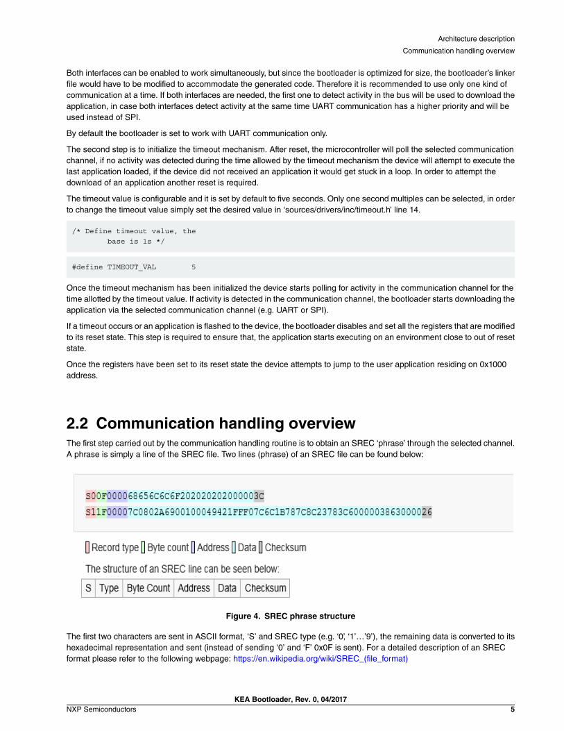
Both interfaces can be enabled to work simultaneously, but since the bootloader is optimized for size, the bootloader’s linkerfile would have to be modified to accommodate the generated code. Therefore it is recommended to use only one kind ofcommunication at a time. If both interfaces are needed, the first one to detect activity in the bus will be used to download theapplication, in case both interfaces detect activity at the same time UART communication has a higher priority and will beused instead of SPI.
By default the bootloader is set to work with UART communication only.
The second step is to initialize the timeout mechanism. After reset, the microcontroller will poll the selected communicationchannel, if no activity was detected during the time allowed by the timeout mechanism the device will attempt to execute thelast application loaded, if the device did not received an application it would get stuck in a loop. In order to attempt thedownload of an application another reset is required.
The timeout value is configurable and it is set by default to five seconds. Only one second multiples can be selected, in orderto change the timeout value simply set the desired value in ‘sources/drivers/inc/timeout.h’ line 14.
/* Define timeout value, the base is 1s */
#define TIMEOUT_VAL 5
Once the timeout mechanism has been initialized the device starts polling for activity in the communication channel for thetime allotted by the timeout value. If activity is detected in the communication channel, the bootloader starts downloading theapplication via the selected communication channel (e.g. UART or SPI).
If a timeout occurs or an application is flashed to the device, the bootloader disables and set all the registers that are modifiedto its reset state. This step is required to ensure that, the application starts executing on an environment close to out of resetstate.
Once the registers have been set to its reset state the device attempts to jump to the user application residing on 0x1000address.
2.2 Communication handling overviewThe first step carried out by the communication handling routine is to obtain an SREC ‘phrase’ through the selected channel.A phrase is simply a line of the SREC file. Two lines (phrase) of an SREC file can be found below:
Figure 4. SREC phrase structure
The first two characters are sent in ASCII format, ‘S’ and SREC type (e.g. ‘0’, ‘1’…’9’), the remaining data is converted to itshexadecimal representation and sent (instead of sending ‘0’ and ‘F’ 0x0F is sent). For a detailed description of an SRECformat please refer to the following webpage: https://en.wikipedia.org/wiki/SREC_(file_format)
Architecture description
Communication handling overview
KEA Bootloader, Rev. 0, 04/2017NXP Semiconductors 5

The phrase is received and stored in the following structure:
typedefunion
{uint8_t Byte [MAX_PHSIZE_BP]; /* Byte level access to the Phrase */
struct{
char PhraseType ; /* Type of received record (e.g. S0, S1, S5, S9...) */ uint8_t PhraseSize ; /* Phrase size (address + data + checksum) *//* Address, depending on the type of record it might vary */ uint8_t PhraseAddress [MAX_ADDRESS_BP]__attribute__ ((aligned (32)));/* Maximum 32 data bytes */uint8_t PhraseData [MAX_DATA_BP]__attribute__ ((aligned (32)));uint8_t PhraseCRC ; /* Checksum of size + address + data */
} F ;
} BootPhraseStruct ;
This structure holds all the information provided by the SREC phrase, such as record type, byte count, address, data andcyclic redundancy check (CRC).
Once the structure has been populated it is checked to verify that it contains a valid record type (i.e. within ‘0’ and ‘9’), itssize is within the SREC maximum and also the CRC is computed with the received data and compared with the CRC thatwas received. If any of these conditions are not met, i.e. invalid record type, invalid record size or CRC does not match, anERR_CRC (0x41) signal is sent back to the device that is sending the data. If everything is received without issues thereceived data is processed and an ERR_OK (0x45) signal is sent as an acknowledge.
If the type of record received carries the data to write to the microcontroller (either ‘1’, ‘2’ or ‘3’) then the data is processedand written by the memory handling layer.
This process is repeated until the termination record is received (either ‘7’, ‘8’ or ‘9’), once this record is received thecommunication handling routine ends and returns to the bootloader.
Architecture description
Communication handling overview
KEA Bootloader, Rev. 0, 04/20176 NXP Semiconductors
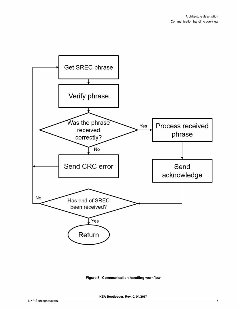
Figure 5. Communication handling workflow
Architecture description
Communication handling overview
KEA Bootloader, Rev. 0, 04/2017NXP Semiconductors 7
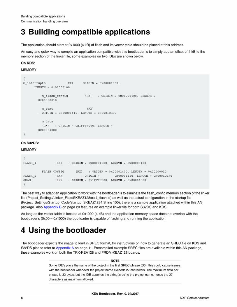
3 Building compatible applications
The application should start at 0x1000 (4 kB) of flash and its vector table should be placed at this address.
An easy and quick way to compile an application compatible with this bootloader is to simply add an offset of 4 kB to thememory section of the linker file, some examples on two IDEs are shown below.
On KDS:
MEMORY
{m_interrupts (RX) : ORIGIN = 0x00001000, LENGTH = 0x00000100 m_flash_config (RX) : ORIGIN = 0x00001400, LENGTH = 0x00000010 m_text (RX) : ORIGIN = 0x00001410, LENGTH = 0x0001DBF0 m_data (RW) : ORIGIN = 0x1FFFF000, LENGTH = 0x00004000}
On S32DS:
MEMORY
{FLASH_1 (RX) : ORIGIN = 0x00001000, LENGTH = 0x00000100 FLASH_CONFIG (RX) : ORIGIN = 0x00001400, LENGTH = 0x00000010FLASH_2 (RX) : ORIGIN = 0x00001410, LENGTH = 0x0001DBF0SRAM (RW) : ORIGIN = 0x1FFFF000, LENGTH = 0x00004000}
The best way to adapt an application to work with the bootloader is to eliminate the flash_config memory section of the linkerfile (Project_Settings/Linker_Files/SKEAZ128xxx4_flash.ld) as well as the actual configuration in the startup file(Project_Settings/Startup_Code/startup_SKEAZ1284.S line 100), there is a sample application attached within this ANpackage. Also Appendix B on page 20 features an example linker file for both S32DS and KDS.
As long as the vector table is located at 0x1000 (4 kB) and the application memory space does not overlap with thebootloader’s (0x00 – 0x1000) the bootloader is capable of flashing and running the application.
4 Using the bootloader
The bootloader expects the image to load in SREC format, for instructions on how to generate an SREC file on KDS andS32DS please refer to Appendix A on page 11. Precompiled example SREC files are available within this AN package,these examples work on both the TRK-KEA128 and FRDM-KEAZ128 boards.
Some IDE’s place the name of the project in the first SREC phrase (S0), this could cause issues
with the bootloader whenever the project name exceeds 27 characters. The maximum data per
phrase is 32 bytes, but the IDE appends the string ‘.srec’ to the project name, hence the 27
characters as maximum allowed.
NOTE
Building compatible applications
Communication handling overview
KEA Bootloader, Rev. 0, 04/20178 NXP Semiconductors
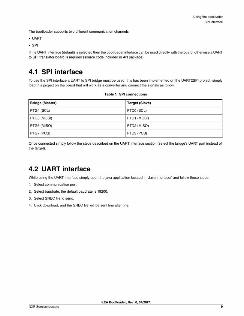
The bootloader supports two different communication channels:
• UART
• SPI
If the UART interface (default) is selected then the bootloader interface can be used directly with the board, otherwise a UARTto SPI translator board is required (source code included in AN package).
4.1 SPI interfaceTo use the SPI interface a UART to SPI bridge must be used, this has been implemented on the UART2SPI project, simplyload this project on the board that will work as a converter and connect the signals as follow:
Table 1. SPI connections
Bridge (Master) Target (Slave)
PTG4 (SCL) PTD0 (SCL)
PTG5 (MOSI) PTD1 (MOSI)
PTG6 (MISO) PTD2 (MISO)
PTG7 (PCS) PTD3 (PCS)
Once connected simply follow the steps described on the UART interface section (select the bridge’s UART port instead ofthe target).
4.2 UART interfaceWhile using the UART interface simply open the java application located in ‘Java interface/’ and follow these steps:
1. Select communication port.
2. Select baudrate, the default baudrate is 19200.
3. Select SREC file to send.
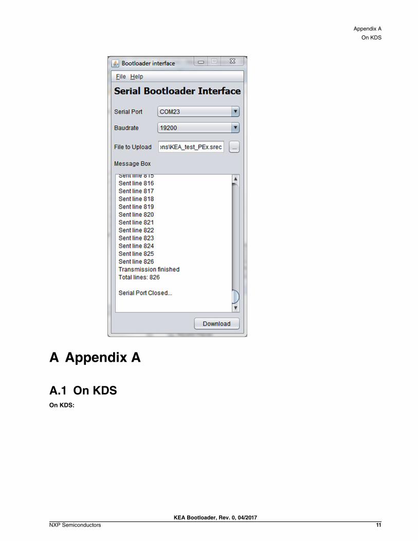
4. Click download, and the SREC file will be sent line after line.
Using the bootloader
SPI interface
KEA Bootloader, Rev. 0, 04/2017NXP Semiconductors 9
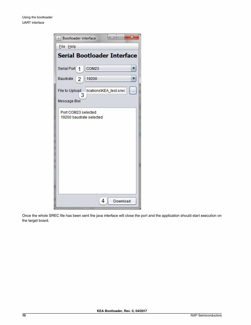
Once the whole SREC file has been sent the java interface will close the port and the application should start execution onthe target board.
Using the bootloader
UART interface
KEA Bootloader, Rev. 0, 04/201710 NXP Semiconductors
A Appendix A
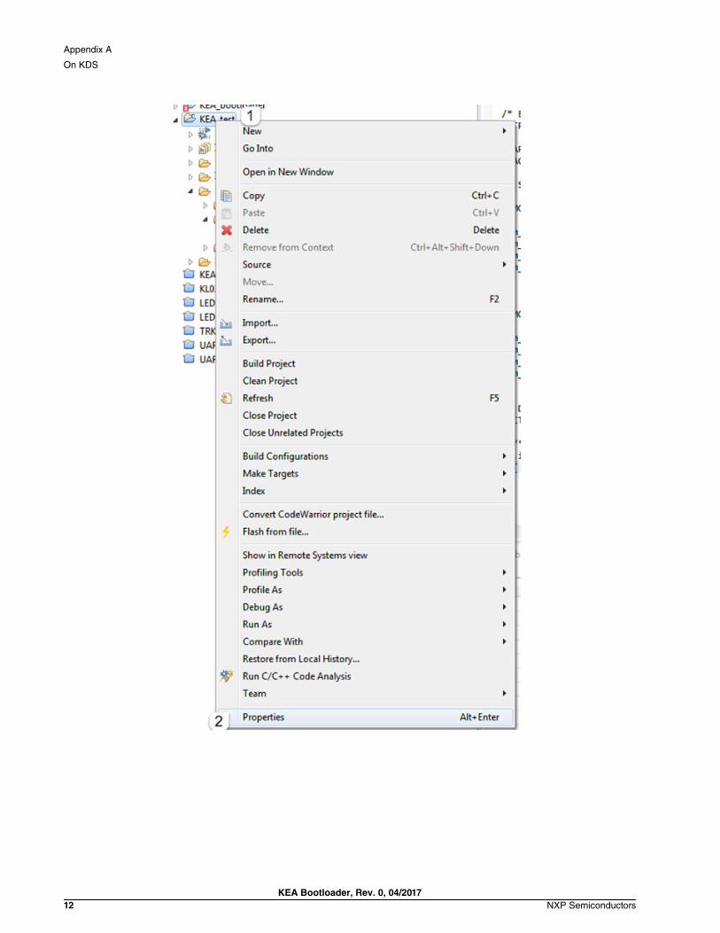
A.1 On KDSOn KDS:
Appendix A
On KDS
KEA Bootloader, Rev. 0, 04/2017NXP Semiconductors 11
Appendix A
On KDS
KEA Bootloader, Rev. 0, 04/201712 NXP Semiconductors
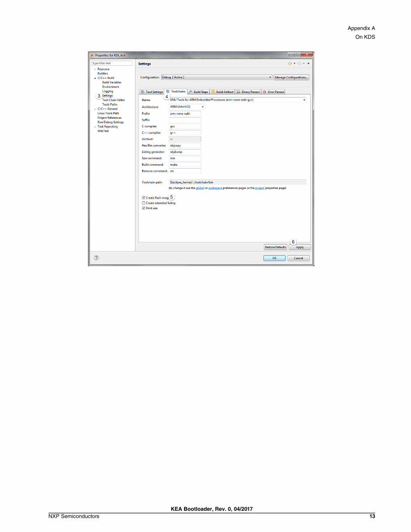
Appendix A
On KDS
KEA Bootloader, Rev. 0, 04/2017NXP Semiconductors 13
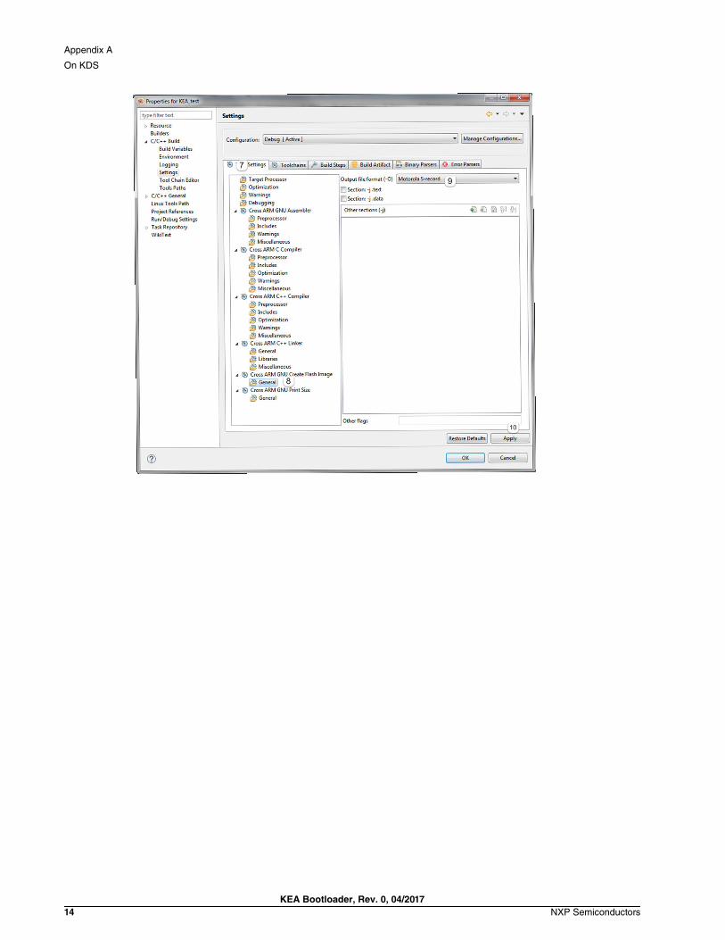
Appendix A
On KDS
KEA Bootloader, Rev. 0, 04/201714 NXP Semiconductors
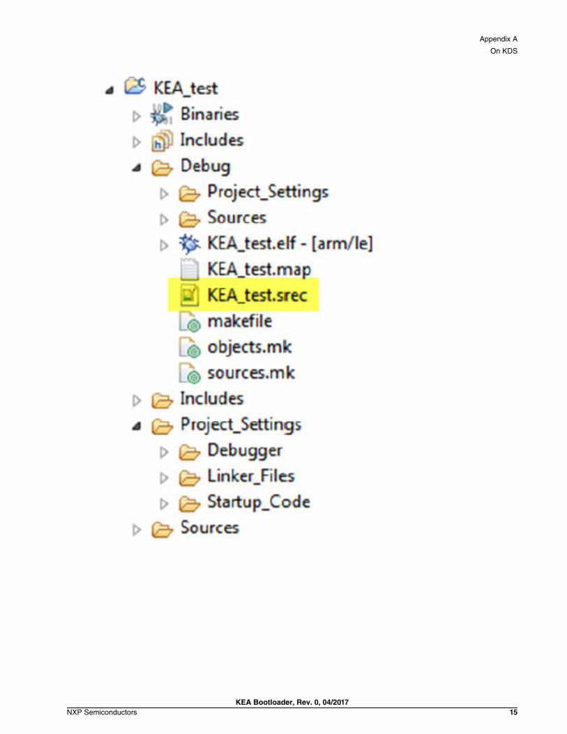
Appendix A
On KDS
KEA Bootloader, Rev. 0, 04/2017NXP Semiconductors 15

A.2 S32DS
Appendix A
S32DS
KEA Bootloader, Rev. 0, 04/201716 NXP Semiconductors

Appendix A
S32DS
KEA Bootloader, Rev. 0, 04/2017NXP Semiconductors 17

Appendix A
S32DS
KEA Bootloader, Rev. 0, 04/201718 NXP Semiconductors

Appendix A
S32DS
KEA Bootloader, Rev. 0, 04/2017NXP Semiconductors 19

B Appendix B
B.1 Linker file on KDS/* Linker file for GNU C Compiler*/
/* Entry Point */ENTRY(Reset_Handler)HEAP_SIZE = DEFINED(__heap_size__) ? __heap_size__ : 0x00000400;STACK_SIZE = DEFINED(__stack_size__) ? __stack_size__ : 0x00000400;
Appendix B
Linker file on KDS
KEA Bootloader, Rev. 0, 04/201720 NXP Semiconductors

/* Specify the memory areas */MEMORY{m_interrupts (RX) : ORIGIN = 0x00001000, LENGTH = 0x00000100m_text (RX) : ORIGIN = 0x00001100, LENGTH = 0x0001EF00m_data (RW) : ORIGIN = 0x1FFFF000, LENGTH = 0x00004000}
/* Define output sections */SECTIONS{/* The startup code goes first into internal flash */.interrupts :{ __VECTOR_TABLE = .; . = ALIGN(4);KEEP(*(.isr_vector)) /* Startup code */. = ALIGN(4);} > m_interrupts
/* The program code and other data goes into internal flash */.text : {. = ALIGN(4);*(.text) /* .text sections (code) */*(.text*) /* .text* sections (code) */*(.rodata) /* .rodata sections (constants, strings, etc.)*/*(.rodata*) /* .rodata* sections (constants, strings, etc.) */*(.glue_7) /* glue arm to thumb code */*(.glue_7t) /* glue thumb to arm code */*(.eh_frame) KEEP (*(.init))KEEP (*(.fini)). = ALIGN(4);} > m_text
.ARM.extab : {*(.ARM.extab* .gnu.linkonce.armextab.*)} > m_text
.ARM :{__exidx_start = .;*(.ARM.exidx*)__exidx_end = .;} > m_text
.ctors : {__CTOR_LIST__ = .;/* gcc uses crtbegin.o to find the start ofthe constructors, so we make sure it isfirst. Because this is a wildcard,itdoesn't matter if the user does notactually link against crtbegin.o; thelinker won't look for a file to match awildcard. The wildcard also means that itdoesn't matter which directory crtbegin.o
Appendix B
Linker file on KDS
KEA Bootloader, Rev. 0, 04/2017NXP Semiconductors 21
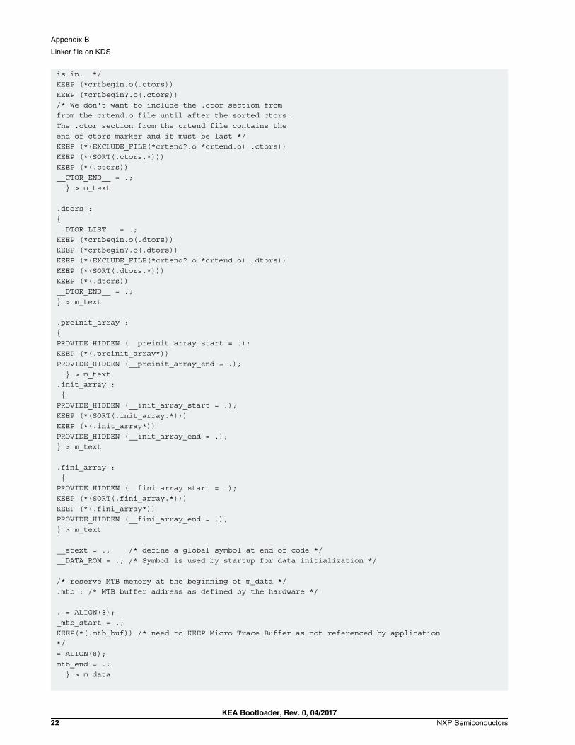
is in. */KEEP (*crtbegin.o(.ctors))KEEP (*crtbegin?.o(.ctors))/* We don't want to include the .ctor section fromfrom the crtend.o file until after the sorted ctors.The .ctor section from the crtend file contains theend of ctors marker and it must be last */ KEEP (*(EXCLUDE_FILE(*crtend?.o *crtend.o) .ctors))KEEP (*(SORT(.ctors.*)))KEEP (*(.ctors))__CTOR_END__ = .; } > m_text
.dtors :{__DTOR_LIST__ = .;KEEP (*crtbegin.o(.dtors))KEEP (*crtbegin?.o(.dtors))KEEP (*(EXCLUDE_FILE(*crtend?.o *crtend.o) .dtors))KEEP (*(SORT(.dtors.*)))KEEP (*(.dtors))__DTOR_END__ = .;} > m_text
.preinit_array :{PROVIDE_HIDDEN (__preinit_array_start = .);KEEP (*(.preinit_array*))PROVIDE_HIDDEN (__preinit_array_end = .); } > m_text.init_array : {PROVIDE_HIDDEN (__init_array_start = .);KEEP (*(SORT(.init_array.*)))KEEP (*(.init_array*))PROVIDE_HIDDEN (__init_array_end = .);} > m_text
.fini_array : {PROVIDE_HIDDEN (__fini_array_start = .);KEEP (*(SORT(.fini_array.*)))KEEP (*(.fini_array*))PROVIDE_HIDDEN (__fini_array_end = .);} > m_text
__etext = .; /* define a global symbol at end of code */__DATA_ROM = .; /* Symbol is used by startup for data initialization */
/* reserve MTB memory at the beginning of m_data */.mtb : /* MTB buffer address as defined by the hardware */
. = ALIGN(8);_mtb_start = .;KEEP(*(.mtb_buf)) /* need to KEEP Micro Trace Buffer as not referenced by application */= ALIGN(8);mtb_end = .; } > m_data
Appendix B
Linker file on KDS
KEA Bootloader, Rev. 0, 04/201722 NXP Semiconductors
.data : AT(__DATA_ROM){. = ALIGN(4);__DATA_RAM = .;__data_start__ = .; /* create a global symbol at data start */*(.data) /* .data sections */*(.data*) /* .data* sections */KEEP(*(.jcr*)). = ALIGN(4);__data_end__ = .; /* define a global symbol at data end */ } > m_data
/* Symbol is used by startup for data initialization */__DATA_END = __DATA_ROM + (__data_end__ - __data_start__);
/* Uninitialized data section */.bss : {/* This is used by the startup in order to initialize the .bss section */. = ALIGN(4);__START_BSS = .;__bss_start__ = .;*(.bss)*(.bss*)*(COMMON). = ALIGN(4);__bss_end__ = .;__END_BSS = .;} > m_data
.heap :{. = ALIGN(8); __end__ = .; PROVIDE(end = .); __HeapBase = .; .+= HEAP_SIZE; __HeapLimit = .; } > m_data.stack : { . = ALIGN(8); . += STACK_SIZE; } > m_data
__StackTop = .; __StackLimit = __StackTop - STACK_SIZE; PROVIDE(__stack = __StackTop); .ARM.attributes 0 : { *(.ARM.attributes) }}
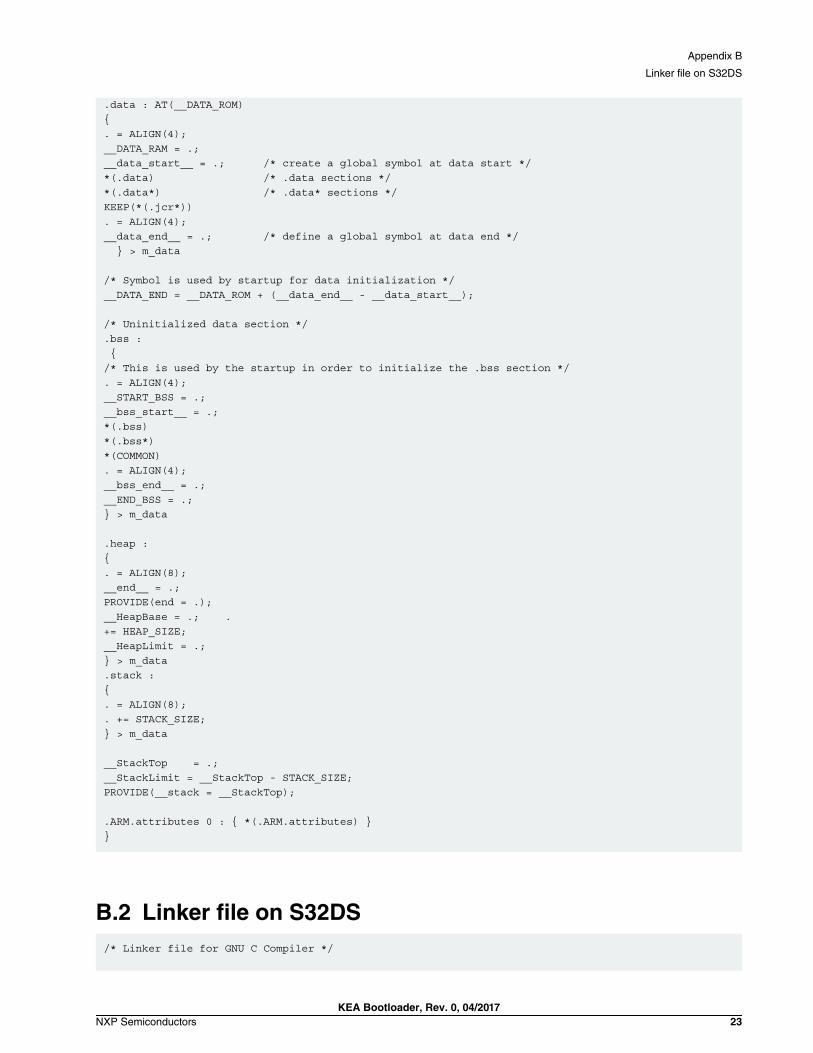
B.2 Linker file on S32DS/* Linker file for GNU C Compiler */
Appendix B
Linker file on S32DS
KEA Bootloader, Rev. 0, 04/2017NXP Semiconductors 23
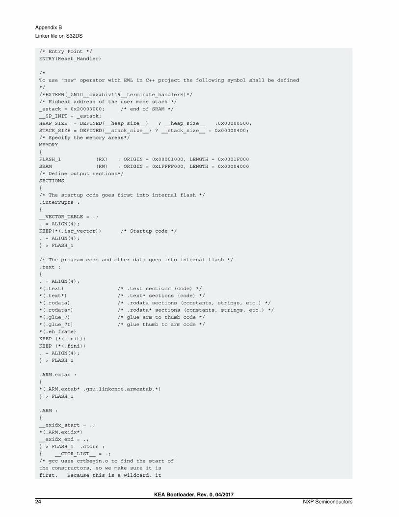
/* Entry Point */ENTRY(Reset_Handler)
/*To use "new" operator with EWL in C++ project the following symbol shall be defined*//*EXTERN(_ZN10__cxxabiv119__terminate_handlerE)*/ /* Highest address of the user mode stack */_estack = 0x20003000; /* end of SRAM */__SP_INIT = _estack;HEAP_SIZE = DEFINED(__heap_size__) ? __heap_size__ :0x00000500;STACK_SIZE = DEFINED(__stack_size__) ? __stack_size__ : 0x00000400; /* Specify the memory areas*/MEMORY{ FLASH_1 (RX) : ORIGIN = 0x00001000, LENGTH = 0x0001F000 SRAM (RW) : ORIGIN = 0x1FFFF000, LENGTH = 0x00004000/* Define output sections*/SECTIONS{ /* The startup code goes first into internal flash */ .interrupts : {__VECTOR_TABLE = .;. = ALIGN(4);KEEP(*(.isr_vector)) /* Startup code */ . = ALIGN(4); } > FLASH_1 /* The program code and other data goes into internal flash */ .text : {. = ALIGN(4); *(.text) /* .text sections (code) */ *(.text*) /* .text* sections (code) */ *(.rodata) /* .rodata sections (constants, strings, etc.) */ *(.rodata*) /* .rodata* sections (constants, strings, etc.) */ *(.glue_7) /* glue arm to thumb code */ *(.glue_7t) /* glue thumb to arm code */ *(.eh_frame) KEEP (*(.init)) KEEP (*(.fini)) . = ALIGN(4); } > FLASH_1 .ARM.extab : {*(.ARM.extab* .gnu.linkonce.armextab.*) } > FLASH_1 .ARM : { __exidx_start = .; *(.ARM.exidx*) __exidx_end = .; } > FLASH_1 .ctors : { __CTOR_LIST__ = .; /* gcc uses crtbegin.o to find the start of the constructors, so we make sure it is first. Because this is a wildcard, it
Appendix B
Linker file on S32DS
KEA Bootloader, Rev. 0, 04/201724 NXP Semiconductors

doesn't matter if the user does not actually link against crtbegin.o; the linker won't look for a file to match a wildcard. The wildcard also means that it doesn't matter which directory crtbegin.o is in. */ KEEP (*crtbegin.o(.ctors)) KEEP (*crtbegin?.o(.ctors))/* We don't want to include the .ctor section from from the crtend.o file until after the sorted ctors. The .ctor section from the crtend file contains the end of ctors marker and it must be last */ KEEP (*(EXCLUDE_FILE(*crtend?.o*crtend.o) .ctors)) KEEP (*(SORT(.ctors.*))) KEEP (*(.ctors)) __CTOR_END__ = .; } > FLASH_1 .dtors : { __DTOR_LIST__ = .; KEEP (*crtbegin.o(.dtors)) KEEP (*crtbegin?.o(.dtors)) KEEP (*(EXCLUDE_FILE(*crtend?.o *crtend.o) .dtors)) KEEP (*(SORT(.dtors.*))) KEEP (*(.dtors)) __DTOR_END__ = .; } > FLASH_1
.preinit_array : { PROVIDE_HIDDEN (__preinit_array_start = .); KEEP (*(.preinit_array*)) PROVIDE_HIDDEN (__preinit_array_end = .); } > FLASH_1 .init_array : { PROVIDE_HIDDEN(__init_array_start = .); KEEP (*(SORT(.init_array.*))) KEEP (*(.init_array*)) PROVIDE_HIDDEN (__init_array_end = .); } > FLASH_1 .fini_array : { PROVIDE_HIDDEN (__fini_array_start = .); KEEP(*(SORT(.fini_array.*))) KEEP (*(.fini_array*)) PROVIDE_HIDDEN (__fini_array_end = .); } > FLASH_1
__etext = .; /* define a global symbol at end of code */ __DATA_ROM = .; /* Symbol is used by startup for data initialization */ /* reserve MTB memory at the beginning of SRAM */ .mtb : /* MTB buffer address as defined by the hardware */ { . = ALIGN(8);
Appendix B
Linker file on S32DS
KEA Bootloader, Rev. 0, 04/2017NXP Semiconductors 25
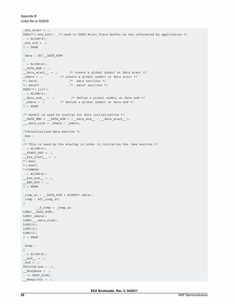
_mtb_start = .; KEEP(*(.mtb_buf)) /* need to KEEP Micro Trace Buffer as not referenced by application */. = ALIGN(8); _mtb_end = .; } > SRAM
.data : AT(__DATA_ROM) { . = ALIGN(4); __DATA_RAM = .; __data_start__ = .; /* create a global symbol at data start */ _sdata = .; /* create a global symbol at data start */ *(.data) /* .data sections */ *(.data*) /* .data* sections */ KEEP(*(.jcr*)) . = ALIGN(4); __data_end__ = .; /* define a global symbol at data end */ _edata = .; /* define a global symbol at data end */ } > SRAM
/* Symbol is used by startup for data initialization */ __DATA_END = __DATA_ROM + (__data_end__ - __data_start__); ___data_size = _edata - _sdata;
/*Uninitialized data section */ .bss : { /* This is used by the startup in order to initialize the .bss section */ . = ALIGN(4); __START_BSS = .; __bss_start__ = .; *(.bss)*(.bss*) *(COMMON) . = ALIGN(4); __bss_end__ = .; __END_BSS = .; } > SRAM
_romp_at = __DATA_ROM + SIZEOF(.data); .romp : AT(_romp_at) { __S_romp = _romp_at; LONG(__DATA_ROM); LONG(_sdata); LONG(___data_size); LONG(0); LONG(0); LONG(0); } > SRAM
.heap : { . = ALIGN(8); __end__ = .; _end = .; PROVIDE(end = .); __HeapBase = .; . += HEAP_SIZE; __HeapLimit = .;
Appendix B
Linker file on S32DS
KEA Bootloader, Rev. 0, 04/201726 NXP Semiconductors

} > SRAM
.stack : { . = ALIGN(8); . += STACK_SIZE; } > SRAM
__StackTop = .; __StackLimit = __StackTop - STACK_SIZE; PROVIDE(__stack = __StackTop); .ARM.attributes 0 : { *(.ARM.attributes) }}
Appendix B
Linker file on S32DS
KEA Bootloader, Rev. 0, 04/2017NXP Semiconductors 27

How To Reach Us
Home Page:
nxp.com
Web Support:
nxp.com/support
Information in this document is provided solely to enable system and software implementers
to use NXP products. There are no express or implied copyright licenses granted hereunder
to design or fabricate any integrated circuits based on the information in this document. NXP
reserves the right to make changes without further notice to any products herein.
NXP makes no warranty, representation, or guarantee regarding the suitability of its products
for any particular purpose, nor does NXP assume any liability arising out of the application
or use of any product or circuit, and specifically disclaims any and all liability, including without
limitation consequential or incidental damages. “Typical” parameters that may be provided in
NXP data sheets and/or specifications can and do vary in different applications, and actual
performance may vary over time. All operating parameters, including “typicals,” must be
validated for each customer application by customer's technical experts. NXP does not convey
any license under its patent rights nor the rights of others. NXP sells products pursuant to
standard terms and conditions of sale, which can be found at the following address: nxp.com/
SalesTermsandConditions.
NXP, the NXP logo, NXP SECURE CONNECTIONS FOR A SMARTER WORLD,
COOLFLUX, EMBRACE, GREENCHIP, HITAG, I2C BUS, ICODE, JCOP, LIFE VIBES,
MIFARE, MIFARE CLASSIC, MIFARE DESFire, MIFARE PLUS, MIFARE FLEX, MANTIS,
MIFARE ULTRALIGHT, MIFARE4MOBILE, MIGLO, NTAG, ROADLINK, SMARTLX,
SMARTMX, STARPLUG, TOPFET, TRENCHMOS, UCODE, Freescale, the Freescale logo,
AltiVec, C‑5, CodeTEST, CodeWarrior, ColdFire, ColdFire+, C‑Ware, the Energy Efficient
Solutions logo, Kinetis, Layerscape, MagniV, mobileGT, PEG, PowerQUICC, Processor
Expert, QorIQ, QorIQ Qonverge, Ready Play, SafeAssure, the SafeAssure logo, StarCore,
Symphony, VortiQa, Vybrid, Airfast, BeeKit, BeeStack, CoreNet, Flexis, MXC, Platform in a
Package, QUICC Engine, SMARTMOS, Tower, TurboLink, and UMEMS are trademarks of
NXP B.V. All other product or service names are the property of their respective owners.
ARM, AMBA, ARM Powered, Artisan, Cortex, Jazelle, Keil, SecurCore, Thumb, TrustZone,
and μVision are registered trademarks of ARM Limited (or its subsidiaries) in the EU and/or
elsewhere. ARM7, ARM9, ARM11, big.LITTLE, CoreLink, CoreSight, DesignStart, Mali, mbed,
NEON, POP, Sensinode, Socrates, ULINK and Versatile are trademarks of ARM Limited (or
its subsidiaries) in the EU and/or elsewhere. All rights reserved. Oracle and Java are
registered trademarks of Oracle and/or its affiliates. The Power Architecture and Power.org
word marks and the Power and Power.org logos and related marks are trademarks and
service marks licensed by Power.org.
Ⓒ 2017 NXP B.V.