reconfigurable eco cells for timing closure and ir drop minimization
DESCRIPTION
Reconfigurable ECO Cells for Timing Closure and IR Drop Minimization. TingTing Hwang Tsing Hua University, Hsin-Chu. Outline. Introduction Engineering Change Order (ECO) Voltage drop (IR-DROP) New design style Cell level Chip level New design style for ECO flow RECON ECO algorithm - PowerPoint PPT PresentationTRANSCRIPT

1
Reconfigurable ECO Cells for Timing Closure and IR Drop Minimization
TingTing HwangTsing Hua University, Hsin-Chu
2
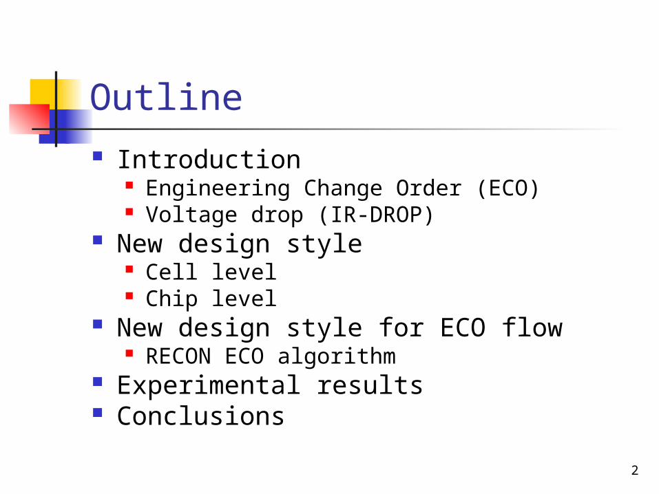
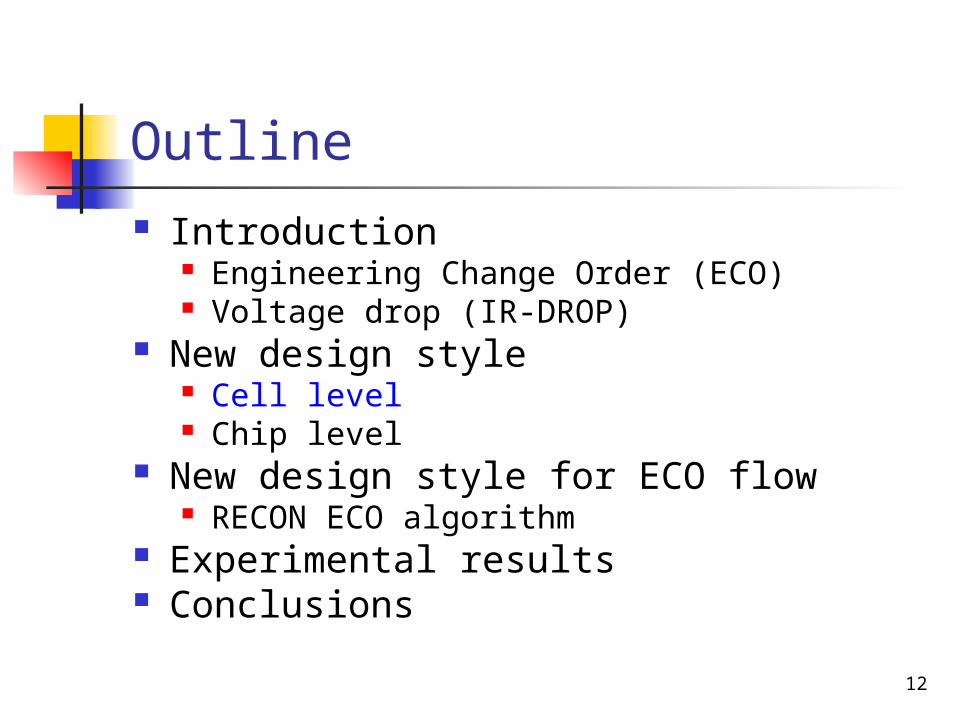
Outline Introduction
Engineering Change Order (ECO) Voltage drop (IR-DROP)
New design style Cell level Chip level
New design style for ECO flow RECON ECO algorithm
Experimental results Conclusions

3
Outline Introduction
Engineering Change Order (ECO) Voltage drop (IR-DROP)
New design style Cell level Chip level
New design style for ECO flow RECON ECO algorithm
Experimental results Conclusions
5
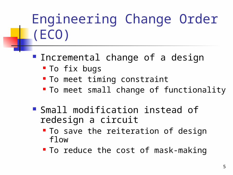
Engineering Change Order (ECO)
Incremental change of a design To fix bugs To meet timing constraint To meet small change of functionality
Small modification instead of redesign a circuit To save the reiteration of design flow To reduce the cost of mask-making

6
Spare Cells in ECO
Spare cells (NOT, NOR, NAND) are placed evenly in layout at physical design
Spare cells are then used for modification in ECO flow
7
Outline Introduction
Engineering Change Order (ECO) Voltage drop (IR-DROP)
New design style Cell level Chip level
New design style for ECO flow RECON ECO algorithm
Experimental results Conclusions

8
Voltage Drop
Power source fluctuations become serious High performance Lower supply voltage
VDD/GND variations Chip speed Noise margin
Adding decoupling capacitance (decap) is an effective way to reduce power noise [Sachin, TCAD 2003]
11
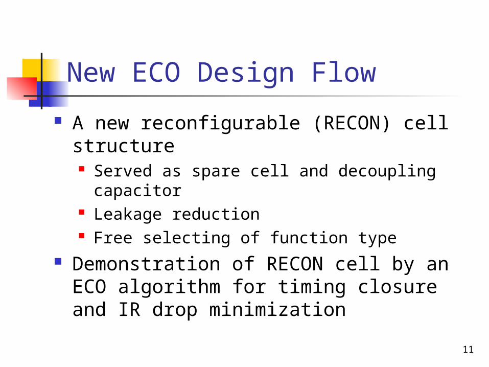
New ECO Design Flow
A new reconfigurable (RECON) cell structure Served as spare cell and decoupling capacitor Leakage reduction Free selecting of function type
Demonstration of RECON cell by an ECO algorithm for timing closure and IR drop minimization
12
Outline Introduction
Engineering Change Order (ECO) Voltage drop (IR-DROP)
New design style Cell level Chip level
New design style for ECO flow RECON ECO algorithm
Experimental results Conclusions

13
RECON Base Cell
Two PMOS transistor with same transistor width
Two NMOS transistor with same transistor width
Eight CONTACTs VDD and GND impleme
nted by layer of metal-1

15
DECAP Cell
Configured from RECON base cellUse Metal-1 connectionSchematic of cell
GND
VDD
VDD
GND
16
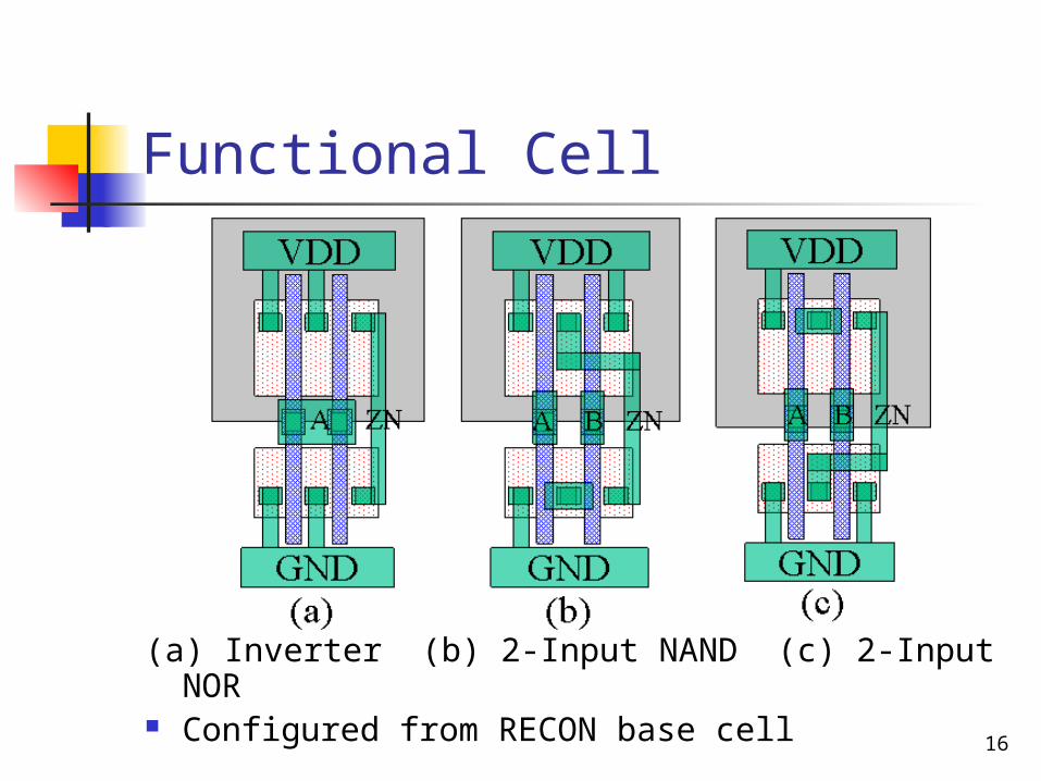
Functional Cell
(a) Inverter (b) 2-Input NAND (c) 2-Input NOR Configured from RECON base cell

17
Comparisons Between RECON Cells and Standard Cells
Setup of experiment Cell layouts created with TSMC
0.13um process SPICE net-lists extracted by RC-
extractor Delay, leakage, internal power
and input pin capacitance by SPICE simulation

18
As Decoupling Cells
Less flexibility of layout 16%-39% capacitance 9%-34% leakage

20
As Functional Cells
Area
Delay
LeakagePowe
rPin capw/o tie-
cellw/i tie-cell Recon w/o tie-
cellw/i tie-cell Recon
INVX1 0.50 1 0.67 1.02 0.88 1 0.81 0.89 0.93
INVX2 0.57 1 0.57 1.01 0.94 1 0.93 0.94 0.94
INVX4 0.67 1 0.89 0.99 0.97 1 0.93 0.98 0.98
INVX8 0.79 1 1.14 0.98 0.98 1 0.89 1.02 0.98
INVX16 0.88 1 1.33 0.98 0.99 1 0.87 1.00 0.99
ND2X1 0.40 1 0.40 1.05 0.8 1 0.80 1.19 0.98
ND2X2 0.50 1 0.67 1.05 0.89 1 0.84 1.30 0.98
NR2X1 0.40 1 0.40 1.09 0.81 1 0.79 1.33 0.98
NR2X2 0.50 1 0.67 1.11 0.89 1 0.86 1.55 1.04
BUFX1 0.57 1 0.57 0.84 0.92 1 1.21 1.07 1.50
BUFX2 0.63 1 1.00 1.00 0.96 1 0.93 0.97 0.95
BUFX4 0.75 1 1.00 0.99 0.98 1 0.90 0.98 0.92
BUFX8 0.83 1 1.33 0.99 0.99 1 0.88 0.99 0.96
Average
0.61 1 0.82 1.01 0.92 1 0.90 1.09 1.01

21
Outline Introduction
Engineering Change Order (ECO) Voltage drop (IR-DROP)
New design style Cell level Chip level
New design style for ECO flow RECON ECO algorithm
Experimental results Conclusions

22
Model of Power Supply Analysis
Cycle-based time frame

23
Model of Power Supply Analysis (cont.)
Metal layer of VDD and GND modeled as a power-grid resistance
Standard cells modeled as time-varying current source
RECON DECAP cells modeled as capacitors connected between VDD and GND

24
Model of Power Supply Analysis (cont.)
Supply voltage variation can be derived as following
Clock cycle is divided into many time slots
Switching gate are derived from static timing analysis
Maximum current consumption are calculated in each time slot.

26
IR Drop Analysis of Whole Chip

27
Leakage Analysis of Whole Chip

28
Outline Introduction
Engineering Change Order (ECO) Voltage Drop (IR-DROP)
New design style Cell level Chip level
New design style for ECO flow RECON ECO algorithm
Experimental result Conclusion
29
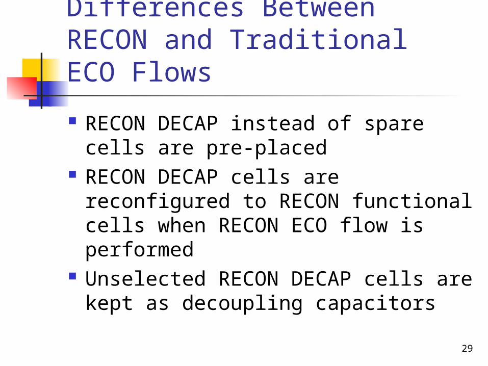
Differences Between RECON and Traditional ECO Flows
RECON DECAP instead of spare cells are pre-placed
RECON DECAP cells are reconfigured to RECON functional cells when RECON ECO flow is performed
Unselected RECON DECAP cells are kept as decoupling capacitors
30
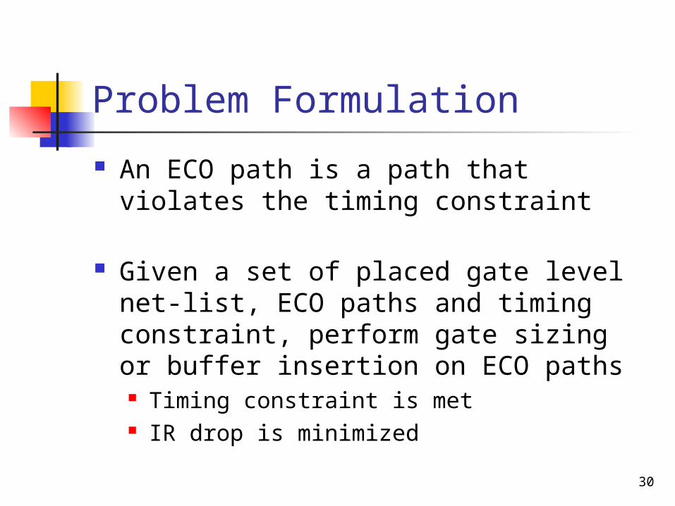
Problem Formulation
An ECO path is a path that violates the timing constraint
Given a set of placed gate level net-list, ECO paths and timing constraint, perform gate sizing or buffer insertion on ECO paths Timing constraint is met IR drop is minimized

32
RECON ECO Algorithm
Input: a set of ECO paths to be optimizedFor each ECO path
Find the critical gates in ECO paths and put in ECO_gate_list While (timing is not satisfy)
Choose the gate from ECO_gate_list with most output loading
Perform gate sizing or buffer insertionList_A = search_region(gate_sizing)List_B = search_region(buffer_insertion)For all configurable cell Rg in List_A or List_B
If IRdrop(Rg) > threshold Remove Rg in List_A or List_B
Candidate_list = List_A + List_B Compute path delay gain for all Rg in Candidate_listSelect the best Rg corresponding to the best delay gainUpdate the ECO path delay
End while
33
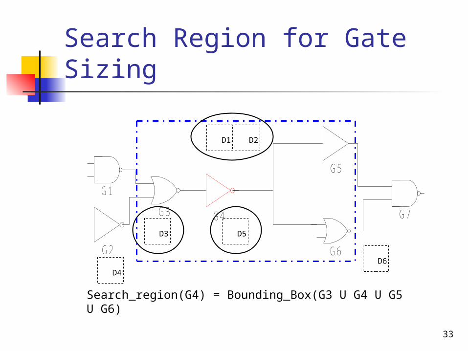
Search Region for Gate Sizing
D1 D2
D3
D4
D5
D6
Search_region(G4) = Bounding_Box(G3 U G4 U G5 U G6)
G6
G1
G4G3
G2
G5
G7

34
Search Region for Buffer Insertion
D1 D2
D3
D4
D5
D6
Search_region(G4) = Bounding_Box(G4 U G5 U G6)
G6
G1
G4G3
G2
G5
G7

35
Outline Introduction
Engineering Change Order (ECO) Voltage drop (IR-DROP)
New design style Cell level Chip level
New design style for ECO flow RECON ECO algorithm
Experimental results Conclusions

36
Experimental Setup
ITC99 benchmarks Benchmarks synthesized to gate-level
net-list using TSMC 0.13um process Standard cells and RECON DECAP cell
s placed by SOCEncounter 20% area used to place RECON DECAP
cells
37
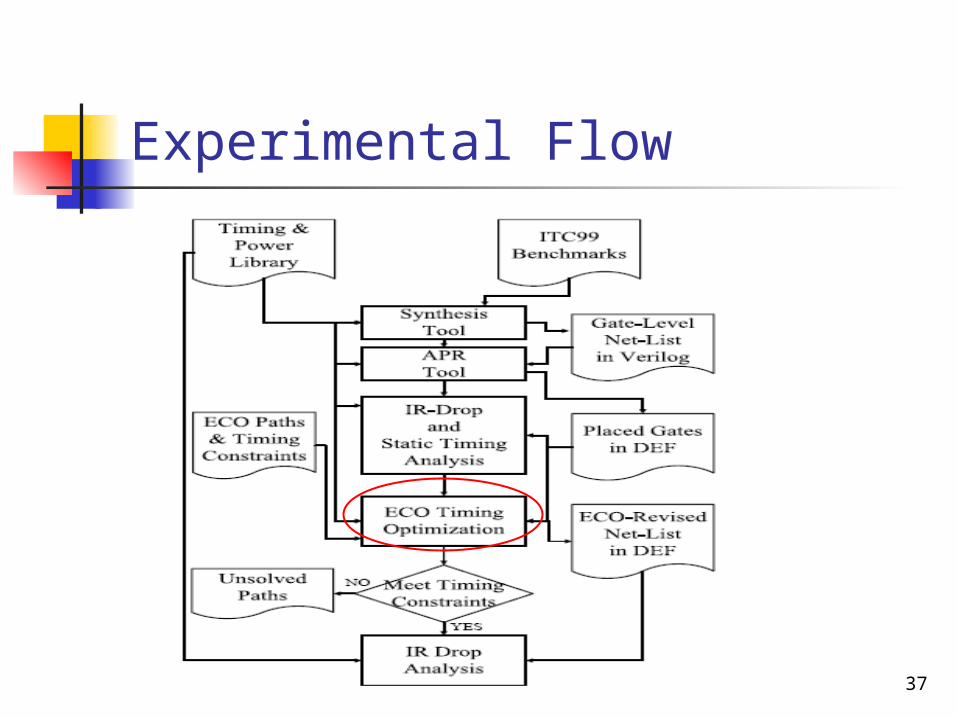
Experimental Flow
38
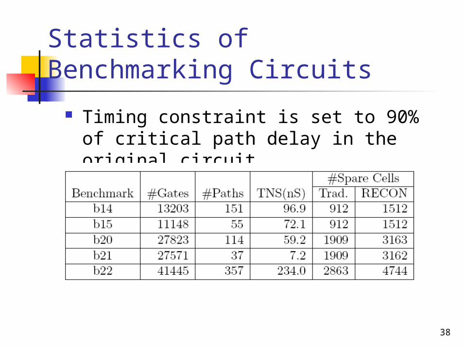
Statistics of Benchmarking Circuits
Timing constraint is set to 90% of critical path delay in the original circuit

39
Leakage Comparisons Before ECO
Leakage comparison
0
10000
20000
30000
40000
50000
60000
b14 b15 b20 b21 b22
benchmark set
Lea
kage
(nA
)
with traditional spare cells
with RECON DECAP cells

40
Performance Comparisons Before ECO
Trad: traditional spare cells RECON: RECON decap cells
41
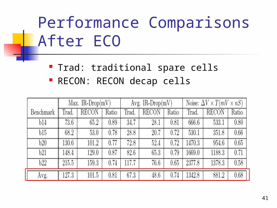
Performance Comparisons After ECO
Trad: traditional spare cells RECON: RECON decap cells

42
Number of Unsolved Paths After ECO
Trad: traditional spare cells RECON: RECON decap cell
43
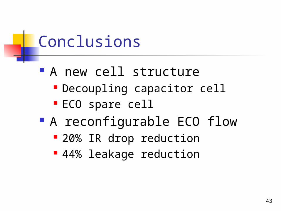
Conclusions
A new cell structure Decoupling capacitor cell ECO spare cell
A reconfigurable ECO flow 20% IR drop reduction 44% leakage reduction

44