rec. itu-r bt.1120-1 1 recommendation itu-r … · digital representation of r, g, b, y, cr and cb...
TRANSCRIPT

Rec. ITU-R BT.1120-1 1
RECOMMENDATION ITU-R BT.1120-1
DIGITAL INTERFACES FOR 1125/60/2:1 AND1250/50/2:1 HDTV STUDIO SIGNALS
(Question ITU-R 65/11)
(1994-1998)Rec. ITU-R BT.1120-1
The ITU Radiocommunication Assembly,
considering
a) that in the scope of Recommendation ITU-R BT.709 studio standards for HDTV have been developed;
b) that Recommendation ITU-R BT.1200 specifies a flexible system description based on the carriage ofdeclarable parameter values;
c) that there exist signal specifications for HDTV studio systems based on 1125 lines, 60 Hz field rate,2:1 interlace and 1250 lines, 50 Hz field rate, 2:1 interlace, based on the above Recommendations;
d) that a whole range of equipment based on the above systems has been developed and is commerciallyavailable, including all those necessary for broadcasting chains and for industrial applications;
e) that many programmes are being produced in both systems using the above equipments and that in thedevelopment of broadcasting and other services there is an increasing need for HDTV production installations;
f) that the use of digital technology and digital interconnection is highly desirable to reach and maintain the levelof performance required for HDTV;
g) that there are clear advantages for establishing interface specifications for HDTV production installations,
recommends
that the specifications described in this Recommendation should be used as the basic digital coding as well asthe bit-parallel and bit-serial interfaces for the 1125/60 and 1250/50 studio signals.
1 Digital representation
1.1 Coding characteristics
The signals to be digitized should comply with the characteristics described in Recommendation ITU-R BT.709.
1.2 Construction of digital signals
Digital representation of R, G, B, Y, CR and CB may be obtained using the following relationship. Further study isrequired in terms of conversion between the data obtained with 8- and 10-bit quantization.
Rd = [ Int (219 × D) × E’R + (16 × D) + 0.5 ] / D
Gd = [ Int (219 × D) × E’G + (16 × D) + 0.5 ] / D
Bd = [ Int (219 × D) × E’B + (16 × D) + 0.5 ] / D
Yd = [ Int (219 × D) × E’Y + (16 × D) + 0.5 ] / D
CRd = [ Int (224 × D) × E’CR + (128 × D) + 0.5 ] / D
CBd = [ Int (224 × D) × E’CB + (128 × D) + 0.5 ] / D
where D takes either the value 1 or 4, corresponding to 8-bit or 10-bit quantization respectively; E’G, E’B, E’R and E’Ydenote analogue R, G, B and luminance signals that have been normalized to span the range 0.0 to 1.0, while E’CR
and E’CB denote analogue colour-difference signals that have been normalized to span the range – 0.5 to + 0.5.
2 Rec. ITU-R BT.1120-1
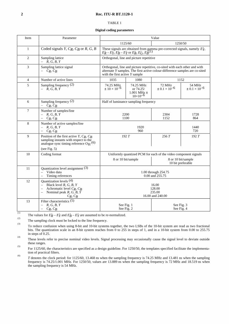
TABLE 1
Digital coding parameters
Item Parameter Value
1125/60 1250/50
1 Coded signals Y, CR, CB or R, G, B These signals are obtained from gamma pre-corrected signals, namely E’Y,E’R – E’Y, E’B – E’Y or E’R, E’G, E’B
(1)
2 Sampling lattice– R, G, B, Y
Orthogonal, line and picture repetitive
3 Sampling lattice signal– CR, CB
Orthogonal, line and picture repetitive, co-sited with each other and withalternate Y samples. The first active colour-difference samples are co-sitedwith the first active Y sample
4 Number of active lines 1035 1080 1152
5 Sampling frequency (2)– R, G, B, Y
74.25 MHz± 10 × 10–6
74.25 MHzor 74.25/
1.001 MHz ±10×10–6
72 MHz± 0.1 × 10⁻⁶
54 MHz± 0.1 × 10⁻⁶
6 Sampling frequency (2)– CR, CB
Half of luminance sampling frequency
7 Number of samples/line– R, G, B, Y– CR, CB
22001100
23041152
1728864
8 Number of active samples/line– R, G, B, Y– CR, CB
1920960
1440720
9 Position of the first active Y, CR, CBsampling instants with respect to theanalogue sync timing reference OH (6)
192 T 256 T 192 T
(see Fig. 5)
10 Coding format Uniformly quantized PCM for each of the video component signals
8 or 10 bit/sample 8 or 10 bit/sample10 bit preferable
11 Quantization level assignment (3)– Video data– Timing references
1.00 through 254.750.00 and 255.75
12 Quantization levels (4)– Black level R, G, B, Y– Achromatic level CR, CB– Nominal peakR, G, B, Y
CR, CB
16.00128.00235.00
16.00 and 240.00
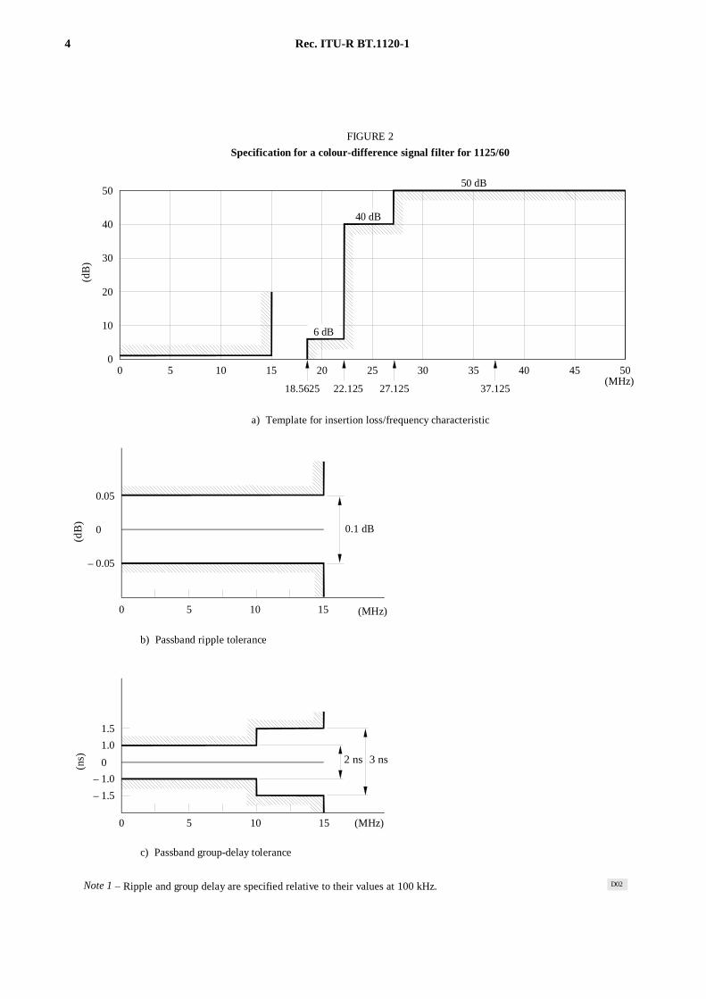
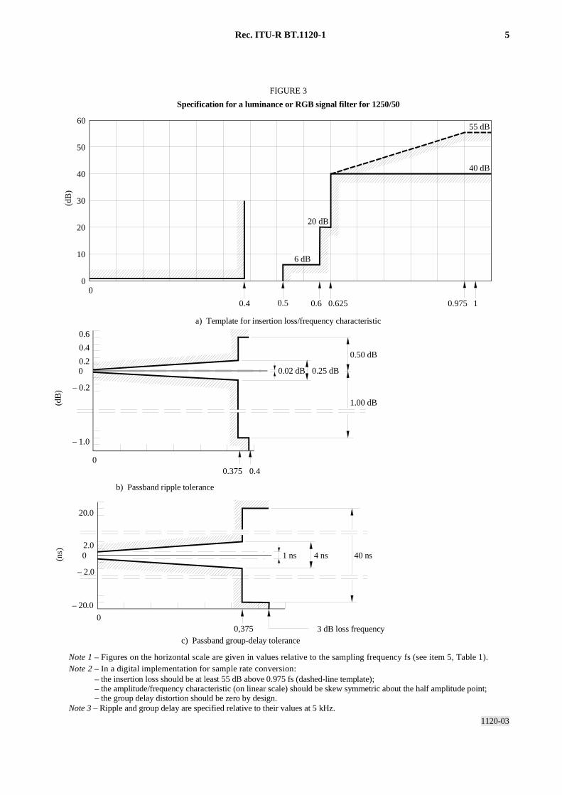
13 Filter characteristics (5)– R, G, B, Y– CR, CB
See Fig. 1See Fig. 2
See Fig. 3 See Fig. 4
(1)The values for E’R – E’Y and E’B – E’Y are assumed to be re-normalized.
(2)The sampling clock must be locked to the line frequency.
(3)To reduce confusion when using 8-bit and 10-bit systems together, the two LSBs of the 10-bit system are read as two fractionalbits. The quantization scale in an 8-bit system reaches from 0 to 255 in steps of 1, and in a 10-bit system from 0.00 to 255.75in steps of 0.25.
(4)These levels refer to precise nominal video levels. Signal processing may occasionally cause the signal level to deviate outsidethese ranges.
(5)For 1125/60, the characteristics are specified as a design guideline. For 1250/50, the templates specified facilitate the implementa-tion of practical filters.
(6)T denotes the clock period: for 1125/60, 13.468 ns when the sampling frequency is 74.25 MHz and 13.481 ns when the samplingfrequency is 74.25/1.001 MHz. For 1250/50, values are 13.889 ns when the sampling frequency is 72 MHz and 18.519 ns whenthe sampling frequency is 54 MHz.

Rec. ITU-R BT.1120-1 3
50 dB
40 dB
12 dB
50
40
30
20
10
00 10 20 30 40 50 60 70 80 90 100
0
0 5 10 15 20 25 30
0
0 5 10 15 20 25 30
D01
FIGURE 1
Specification for a luminance or RGB signal filter for 1125/60
(dB
)(d
B)
(ns)
a) Template for insertion loss/frequency characteristic
0.05
– 0.05
1.5
– 1.5
1.0
– 1.0
37.125 44.25 54.25 74.25
b) Passband ripple tolerance
(MHz)
(MHz)
0.1 dB
c) Passband group-delay tolerance
(MHz)
Note 1 – Ripple and group delay are specified relative to their values at 100 kHz.
2 ns 3 ns
4 Rec. ITU-R BT.1120-1
50 dB
40 dB
6 dB
50
40
30
20
10
00 5 10 15 20 25 30 35 40 45 50
0
0 5 10 15
0
0 5 10 15
FIGURE 2
Specification for a colour-difference signal filter for 1125/60
(dB
)(d
B)
(ns)
a) Template for insertion loss/frequency characteristic
b) Passband ripple tolerance
(MHz)
(MHz)
c) Passband group-delay tolerance
(MHz)
Note 1 – Ripple and group delay are specified relative to their values at 100 kHz.
2 ns 3 ns
D02
0.05
– 0.05
18.5625 22.125 27.125 37.125
1.0
– 1.0
1.5
– 1.5
0.1 dB
Rec. ITU-R BT.1120-1 5
1120-03
0
(dB
)
0
00,375
1 ns 4 ns 40 ns(ns) 0
55 dB
50
40
30
20
10
00
60
(dB
)
1
40 dB
20 dB
6 dB
FIGURE 3
Specification for a luminance or RGB signal filter for 1250/50
c) Passband group-delay tolerance
– 2.0
2.0
20.0
– 20.0
3 dB loss frequency
a) Template for insertion loss/frequency characteristic
0.4 0.5 0.6 0.625 0.975
b) Passband ripple tolerance
0.50 dB
0.02 dB 0.25 dB
1.00 dB
– 1.0
– 0.2
0.4
0.6
0.2
0.375 0.4
Note 2 – In a digital implementation for sample rate conversion:– the insertion loss should be at least 55 dB above 0.975 fs (dashed-line template);– the amplitude/frequency characteristic (on linear scale) should be skew symmetric about the half amplitude point;– the group delay distortion should be zero by design.
Note 3 – Ripple and group delay are specified relative to their values at 5 kHz.
Note 1 – Figures on the horizontal scale are given in values relative to the sampling frequency fs (see item 5, Table 1).

6 Rec. ITU-R BT.1120-1
1120-04
55 dB
40 dB
50
40
30
20
10
00
6 dB
20 dB
60
(dB
)
0
0
(dB
)
0
0 2 ns 8 ns 80 ns
(ns)
FIGURE 4
Specification for a colour-difference signal filter for 1250/50
c) Passband group delay tolerance
3 dB loss frequency0.1875
– 40.0
– 4.0
4.0
40.0
b) Passband ripple tolerance
0.02 dB 0.25 dB
0.50 dB
1.00 dB
0.20.1875
0.4
0.6
– 1.0
0.2
– 0.2
a) Template for insertion loss/frequency characteristic
0.250.2 0.3 0.3125 0.4875 0.5
Note 2 – In a digital implementation for sample rate conversion:– the insertion loss should be at least 55 dB above 0.4875 fs (dashed-line template);– the amplitude/frequency characteristic (on linear scale) should be skew symmetric about the half amplitude point;– the group delay distortion should be zero by design.
Note 3 – Ripple and group delay are specified relative to their values at 5 kHz.
Note 1 – Figures on the horizontal scale are given in values relative to the luminance sampling frequency fs (see item 5, Table 1).

Rec. ITU-R BT.1120-1 7
2 Digital interface
The interface provides a unidirectional interconnection between a single source and a single destination. The data signalsare in the form of binary information and are coded accordingly:
– video data (8-bit or 10-bit words for 1125/60 and 1250/50);
– timing reference and identification codes (8-bit or 10-bit words for 1125/60, 10-bit words only for 1250/50);
– ancillary data.
2.1 Video data
Y, CR, CB signals are handled as 20-bit words by time-multiplexing CR and CB components. Each 20-bit wordcorresponds to a colour-difference sample and a luminance sample. The multiplex is organized as:
(CB1 Y1) (CR1 Y2) (CB3 Y3) (CR3 Y4) ...
where Yi indicates the i-th active sample of a line, while CBi and CRi indicate the colour-difference samples of CR andCB components co-sited with the Yi sample. Note that the index “i” on colour-difference samples takes only odd valuesdue to the half-rate sampling of the colour-difference signals.
The data words corresponding to digital levels 0.00 through 0.75 and 255.00 through 255.75 are reserved for dataidentification purposes and must not appear as video data.
For 1125/60, R, G and B signals are handled as 30-bit words in addition to the above 20-bit words for Y, CR and CBsignals.
2.2 Video timing relationship with analogue waveform
For 1125/60, the digital line occupies 2200 clock periods. It begins at 88 clock periods prior to the reference transition(OH) of the analogue synchronizing signal in the corresponding line. The digital active line begins at 192 clock periodsafter the reference transition (OH).
For 1250/50 at 72 MHz sampling frequency, the digital line occupies 2304 clock periods. It begins at 128 clock periodsprior to the reference transition (OH) of the analogue synchronizing signal in the corresponding line. The digital activeline begins at 256 clock periods after the reference transition (OH).
For 1250/50 at 54 MHz sampling rate, the digital line occupies 1728 clock periods. It begins at 96 clock periods prior to
the reference transition (OH) of the analogue synchronizing signal in the corresponding line. The digital active line
begins at 192 clock periods after the reference transition (OH).
See Fig. 5 and Table 2 for detailed timing relationship in the line interval.
The start of digital field is fixed by the position specified for the start of the digital line. See Fig. 6 and Table 3 fordetailed relationship in field interval.
2.3 Video timing reference codes (SAV and EAV)
There are two timing reference codes, one at the beginning of each video data block (start of active video; SAV) and theother at the end of each video data block (end of active video; EAV). These codes are contiguous with the video data,and continue during the field blanking interval, as shown in Fig. 6.
Each code consists of a four-word sequence. The bit assignment of the word is given in Table 4. The first three wordsare fixed preamble and the fourth word carries the information that defines field identification (F), field blanking period(V), and line blanking period (H). In a 1125/60 8 bit implementation bits Nos. 9 to 2 inclusive are used; note in 1250/50all 10 bits are required.
The bits F and V change state synchronously with EAV at the beginning of the digital line.

8 Rec. ITU-R BT.1120-1
FIGURE 5
Data format and timing relationship to analogue waveform
(a)
(k)
(d ) (d)(e)
50%
OH
Analogue active line (b)
Analogue full line (c)
Video data block (h)
(f ) (g)
EAV
SAV
EAV
Video data (Y, R, G, B)
EAV
SAV
EAV
Multiplexed video data (C / C )B R
(i)
Digital active line (l)
Digital line (m)
Analogue line blanking
Digital line blanking
D05
( )j

Rec. ITU-R BT.1120-1 9
TABLE 2
Line interval timing specifications
Symbol Parameter Value
1125/60 1250/50
Number of active Y samples per line 1920 1920 1440
a Analogue line blanking 3.771 µs nominal 6.00 µs nominal
b Analogue active line 25.859 µs nominal 26.00 µs nominal
c Analogue full line 29.630 µs nominal 32.00 µs nominal
d Duration between end of analogueactive video and start of EAV
0-6 T 24 T 18 T
e Duration between end of SAV and startof analogue active video
0-6 T 24 T 18 T
f Duration between start of EAV andanalogue timing reference OH
88 T 128 T 96 T
g Duration between analogue timingreference OH and end of SAV
192 T 256 T 192 T
h Video data block 1928 T 1478 T
i Duration of EAV 4 T
j Duration of SAV 4 T
k Digital line blanking 280 T 384 T 288 T
l Digital active line 1920 T 1440 T
m Digital line 2200 T 2304 T 1728 T
NOTE 1 – T denotes the clock period: for 1125/60, 13.468 ns when the sampling frequency is 74.25 MHz and 13.481 ns whenthe sampling frequency is 74.25/1.001 MHz. For 1250/50, values are 13.889 ns when the sampling frequency is 72 MHz and18.519 ns when the sampling frequency is 54 MHz.

10 Rec. ITU-R BT.1120-1
02
2
02
26
64
46
6
L1
L2L3
L4L5
L6L7
L8L9
L10L11
L127
75
57
73
31
13
3
FIGURE 6
Field timing relationship
Digital line blanking
EAV SAV
1 fr
ame
Fiel
d N
o. 1
Fiel
d N
o. 2
Field No. 1Active video
Field No. 2Active video
Value of (F/V/H) Value of (F/V/H)
Note 1 – The values of (F/V/H) for EAV and SAV represent the status of bits for F, V, and H, in a way that the three-bitword composed of F, V, H represents a binary number expressed in decimal notation (F corresponding to MSB and H to LSB). For example, the value 3 represents the bits of F = 0, V = 1 and H = 1.
D06
1 digital line
Rec. ITU-R BT.1120-1 11
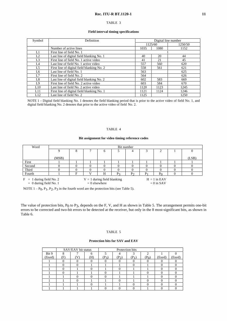
TABLE 3
Field interval timing specifications
TABLE 4
Bit assignment for video timing reference codes
The value of protection bits, P0 to P3, depends on the F, V, and H as shown in Table 5. The arrangement permits one-biterrors to be corrected and two-bit errors to be detected at the receiver, but only in the 8 most-significant bits, as shown inTable 6.
TABLE 5
Protection bits for SAV and EAV
Symbol Definition Digital line number1125/60 1250/50
Number of active lines 1035 1080 1152L1 First line of field No. 1 1L2 Last line of digital field blanking No. 1 40 20 44L3 First line of field No. 1 active video 41 21 45L4 Last line of field No. 1 active video 557 560 620L5 First line of digital field blanking No. 2 558 561 621L6 Last line of field No. 1 563 625L7 First line of field No. 2 564 626L8 Last line of digital field blanking No. 2 602 583 669L9 First line of field No. 2 active video 603 584 670
L10 Last line of field No. 2 active video 1120 1123 1245L11 First line of digital field blanking No. 1 1121 1124 1246L12 Last line of field No. 2 1125 1250
NOTE 1 – Digital field blanking No. 1 denotes the field blanking period that is prior to the active video of field No. 1, anddigital field blanking No. 2 denotes that prior to the active video of field No. 2.
Word Bit number9
(MSB)
8 7 6 5 4 3 2 1 0
(LSB)First 1 1 1 1 1 1 1 1 1 1Second 0 0 0 0 0 0 0 0 0 0Third 0 0 0 0 0 0 0 0 0 0Fourth 1 F V H P3 P2 P1 P0 0 0
F = 1 during field No. 2= 0 during field No. 1
V = 1 during field blanking= 0 elsewhere
H = 1 in EAV= 0 in SAV
NOTE 1 – P0, P1, P2, P3 in the fourth word are the protection bits (see Table 5).
SAV/EAV bit status Protection bitsBit 9
(fixed)8
(F)7
(V)6
(H)5
(P3)4
(P2)3
(P1)2
(P0)1
(fixed)0
(fixed)1 0 0 0 0 0 0 0 0 01 0 0 1 1 1 0 1 0 01 0 1 0 1 0 1 1 0 01 0 1 1 0 1 1 0 0 01 1 0 0 0 1 1 1 0 01 1 0 1 1 0 1 0 0 01 1 1 0 1 1 0 0 0 01 1 1 1 0 0 0 1 0 0

12 Rec. ITU-R BT.1120-1
TABLE 6
Error corrections using protection bits (P3-P0)
2.4 Ancillary data
The ancillary signals should comply with the general rules of Recommendation ITU-R BT.1364.
2.5 Data words during blanking
The data words occurring during digital blanking intervals that are not used for the SAV, the EAV, the timing referencecode ANC, or for ancillary data are filled with words corresponding to the following blanking levels, appropriatelyplaced in the multiplexed data:
16.00 for Y, R, G, B signals
128.00 for CB/CR (time-multiplexed colour-difference signal).
3 Bit-parallel interface
For the 1125/60 system, the bits of the digital code words which describe the video signal are transmitted in parallel bymeans of 20 or 30 shielded conductor pairs. The 20 conductor pairs are used for the transmission of the signal setconsisting of luminance Y and time-multiplexed colour-difference CB/CR components. The 30 conductor pairs are usedfor the transmission of R, G, B signals or Y, CB/CR components with an additional data stream (auxiliary channel). Anadditional shielded conductor pair carries the synchronous clock at 74.25 MHz.
For the 1250/50 system, the bits of the digital code words that describe the video signal are transmitted in parallel bymeans of 20 signal pairs, where each pair carries a stream of bits, 10 pairs for luminance data and 10 pairs for time-multiplexed colour-difference data. The 20 pairs can also carry ancillary data. A 21st pair provides a synchronous clockat 36 MHz (when sampling rate is 72 MHz), or at 27 MHz (when sampling rate is 54 MHz).
Data signals are transmitted in NRZ form in real time (unbuffered).
Receivedbits 5-2
Received bits 8-6 for F, V and H
for P3-P0 000 001 010 011 100 101 110 1110000 000 000 000 – 000 – – 1110001 000 – – 111 – 111 111 1110010 000 – – 011 – 101 – –0011 – – 010 – 100 – – 111
0100 000 – – 011 – – 110 –0101 – 001 – – 100 – – 1110110 – 011 011 011 100 – – 0110111 100 – – 011 100 100 100 –
1000 000 – – – – 101 110 –1001 – 001 010 – – – – 1111010 – 101 010 – 101 101 – 1011011 010 – 010 010 – 101 010 –
1100 – 001 110 – 110 – 110 1101101 001 001 – 001 – 001 110 –1110 – – – 011 – 101 110 –1111 – 001 010 – 100 – – –
NOTE 1 – The error correction applied provides a DEDSEC (double error detection – single errorcorrection) function. The received bits denoted by “–” in the table, if detected, indicate that an error hasoccurred but cannot be corrected.
Rec. ITU-R BT.1120-1 13
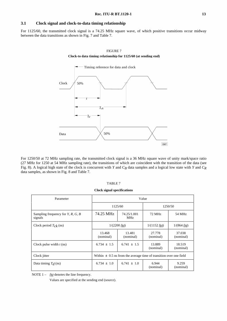
3.1 Clock signal and clock-to-data timing relationship
For 1125/60, the transmitted clock signal is a 74.25 MHz square wave, of which positive transitions occur midwaybetween the data transitions as shown in Fig. 7 and Table 7.
FIGURE 7
Clock-to data timing relationship for 1125/60 (at sending end)
Timing reference for data and clock
50%Clock
t
Tck
Tdo
Data 50%
D07
For 1250/50 at 72 MHz sampling rate, the transmitted clock signal is a 36 MHz square wave of unity mark/space ratio(27 MHz for 1250 at 54 MHz sampling rate), the transitions of which are coincident with the transition of the data (seeFig. 8). A logical high state of the clock is concurrent with Y and CB data samples and a logical low state with Y and CRdata samples, as shown in Fig. 8 and Table 7.
TABLE 7
Clock signal specifications
Parameter Value
1125/60 1250/50
Sampling frequency for Y, R, G, Bsignals
74.25 MHz 74.25/1.001MHz
72 MHz 54 MHz
Clock period Tck (ns) 1/(2200 fH) 1/(1152 fH) 1/(864 fH)
13.468(nominal)
13.481(nominal)
27.778(nominal)
37.038(nominal)
Clock pulse width t (ns) 6.734 ± 1.5 6.741 ± 1.5 13.889(nominal)
18.519(nominal)
Clock jitter Within ± 0.5 ns from the average time of transition over one field
Data timing Td (ns) 6.734 ± 1.0 6.741 ± 1.0 6.944(nominal)
9.259(nominal)
NOTE 1 – fH denotes the line frequency.
Values are specified at the sending end (source).

14 Rec. ITU-R BT.1120-1
D08
FIGURE 8
Clock to data timing relationship for 1250/50
T
Clock
Data
ti
ck
Tdi
Y1
Nominal data detection points
Tdi
Y2CB1 CR1 CB3Y3
3.2 Electrical characteristics of the interface
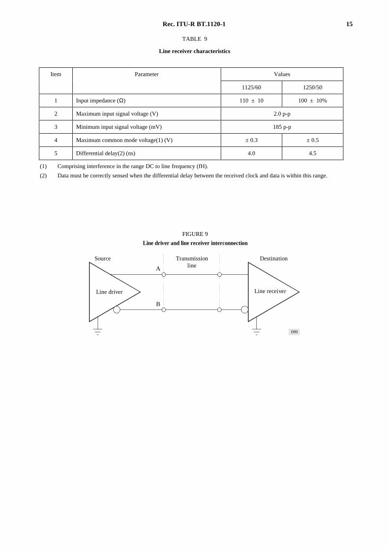
The interface employs 21 line drivers and line receivers, in the case of the transmission of Y and CR/CB components.Each line driver has a balanced output and the corresponding line receiver has a balanced input.
For 1125/60, the interface employs 31 line drivers and line receivers, in the case of R, G and B components or Y, CR/CBwith an additional data stream (auxiliary channel). Although the use of ECL technology is not mandatory, the line driverand receiver must be ECL 10 kH compatible for 1125/60, and ECL 100 k compatible for 1250/50, i.e., they must permitthe use of ECL for either drivers or receivers. The receiver must sense correctly the data when a random signal producesconditions represented by the eye diagram of Fig. 10.
TABLE 8
Line driver characteristics
Item Parameter Values
1125/60 1250/50
1 Output impedance (Ω) 110 maximum 100 maximum
2 Common mode voltage(1) (V) –1.29 ± 15% –1.3 ± 15%
3 Signal amplitude(2) (V) 0.6 to 2.0 p-p 0.8 to 2.0 p-p
4 Rise and fall times(3) (ns) ≤ 2.0 < 3
5 Difference between rise and fall times (ns) ≤ 1.0
(1) Measured relative to ground.
(2) Measured across a resistive load having the nominal impedance of the assumed cables, thatis 110 Ω for 1125/60 and 100 Ω for 1250/50.
(3) Measured between the 20% and 80% points across a resistive load having the nominal impedance of the assumed cable.
Rec. ITU-R BT.1120-1 15
TABLE 9
Line receiver characteristics
A
B
D09
FIGURE 9
Line driver and line receiver interconnection
Source Transmissionline
Line receiver
Destination
Line driver
Item Parameter Values
1125/60 1250/50
1 Input impedance (Ω) 110 ± 10 100 ± 10%
2 Maximum input signal voltage (V) 2.0 p-p
3 Minimum input signal voltage (mV) 185 p-p
4 Maximum common mode voltage(1) (V) ± 0.3 ± 0.5
5 Differential delay(2) (ns) 4.0 4.5
(1) Comprising interference in the range DC to line frequency (fH).
(2) Data must be correctly sensed when the differential delay between the received clock and data is within this range.

16 Rec. ITU-R BT.1120-1
D10
FIGURE 10
Idealized eye diagram corresponding to the minimum input signal level
Tmin Tmin
Reference transition of clock
Note 1 – For 1125/60, the width of the window in the eye diagram, within which data must be correctly detected, comprises ± 0.5 ns clock jitter, ± 1.0 ns data timing, and ± 2.5 ns propagation skew of conductor pairs.
For 1250/50, the aggregate of clock jitter, data timing and propagation skew of conductor pairs must not exceed 4.5 ns.
: 4.0 ns for 1125/60: 4.5 ns for 1250/50: 100 mV
T
V
min
min
Vmin
3.3 Mechanical characteristics
3.3.1 Connector
The interface uses a multi-contact connector. Connectors are locked by two screws on the cable connectors and twothreaded bolts on the equipment. Cable connectors employ pin contacts and equipment connectors employ socketcontacts. Shielding of the connectors and cables is mandatory.
For 1125/60, a 93-contact connector is used. Contact assignments are indicated in Tables 10 and 11. The mechanicalspecifications for the connectors are shown in Figs. 11, 12 and 13.
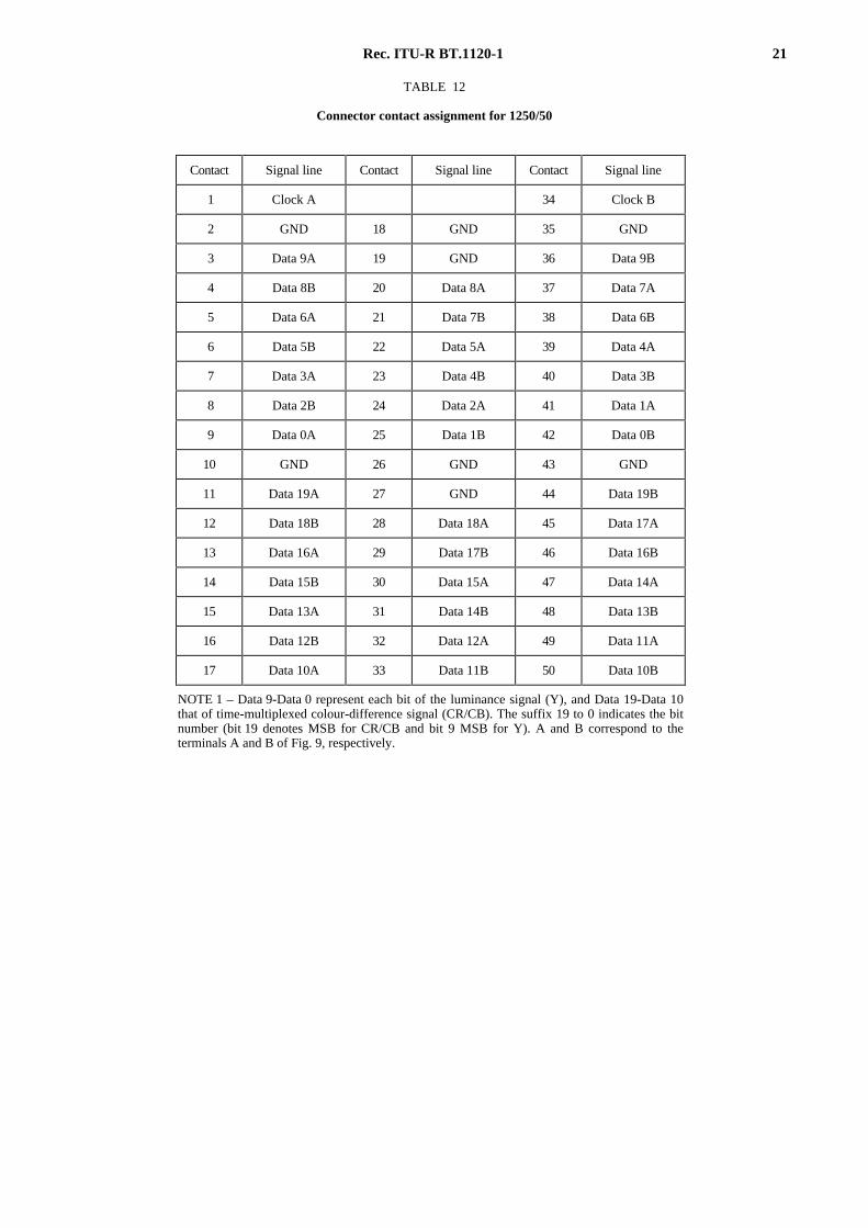
For 1250/50, a 50-contact type D subminiature connector is used. Contact assignments are indicated in Table 12 and Fig.14 (for information, suggested contact assignments for a CB header are shown in Fig. 15).
3.3.2 Interconnecting cable
For 1125/60, two types of multi-channel cable, either 21 or 31 channels, can be used in accordance with the transmissionsignal set (see Table 11). The cable consists of twisted pairs with individual shield of each pair. It also contains anoverall shield. The nominal characteristic impedance of each twisted pair is 110 Ω. The cable shall provide thecharacteristics that satisfy the condition of eye diagram shown in Fig. 10 up to a maximum cable length of 20 m.
For 1250/50, 21-channel balanced conductor pairs is used. The nominal characteristic impedance of each conductor pairis 100 Ω. Cable length up to 30 m may be employed when a high-quality cable is used.

Rec. ITU-R BT.1120-1 17
TABLE 10
Connector contact assignment for 1125/60 system
TABLE 11
Transmission signal set and signal line assignment for 1125/60
Contact Signal line Contact Signal line Contact Signal line Contact Signal line Contact Signal line Contact Signal line
1 Clock A 17 GND 33 Clock B
2 XD 9A 18 GND 34 XD 9B 49 YD 4A 64 GND 79 YD 4B
3 XD 8A 19 GND 35 XD 8B 50 YD 3A 65 GND 80 YD 3B
4 XD 7A 20 GND 36 XD 7B 51 YD 2A 66 GND 81 YD 2B
5 XD 6A 21 GND 37 XD 6B 52 YD 1A 67 GND 82 YD 1B
6 XD 5A 22 GND 38 XD 5B 53 YD 0A 68 GND 83 YD 0B
7 XD 4A 23 GND 39 XD 4B 54 ZD 9A 69 GND 84 ZD 9B
8 XD 3A 24 GND 40 XD 3B 55 ZD 8A 70 GND 85 ZD 8B
9 XD 2A 25 GND 41 XD 2B 56 ZD 7A 71 GND 86 ZD 7B
10 XD 1A 26 GND 42 XD 1B 57 ZD 6A 72 GND 87 ZD 6B
11 XD 0A 27 GND 43 XD 0B 58 ZD 5A 73 GND 88 ZD 5B
12 YD 9A 28 GND 44 YD 9B 59 ZD 4A 74 GND 89 ZD 4B
13 YD 8A 29 GND 45 YD 8B 60 ZD 3A 75 GND 90 ZD 3B
14 YD 7A 30 GND 46 YD 7B 61 ZD 2A 76 GND 91 ZD 2B
15 YD 6A 31 GND 47 YD 6B 62 ZD 1A 77 GND 92 ZD 1B
16 YD 5A 32 GND 48 YD 5B 63 ZD 0A 78 GND 93 ZD 0B
NOTE 1 – XD 9-XD 0, YD 9-YD 0, and ZD 9-ZD 0 represent each bit of the component signals. The suffix 9 to 0 indicates the bitnumber (bit 9 denotes MSB). A and B correspond to the terminals A and B of Fig. 9, respectively. The relationship between XD, YD,ZD and component signals are specified in Table 10.
NOTE 2 – The shield of each pair uses the ground contact (GND) located between A and B contacts for the signal, e.g., contact No.17 is used for the shield of the clock signal. The overall shield of the cable is electrically connected to connector hood, which isgrounded to the frame of the equipment.
Transmission ComponentSignal line assignment
Cablesignal set 10 bit system 8-bit system
Y, CR/CBY XD 9-XD 0 XD 9-XD 2
CR/CB ZD 9-ZD 0 ZD 9-ZD 2 21 pairs
Y, CR/CBY XD 9-XD 0 XD 9-XD 2
with auxiliarychannel CR/CB ZD 9-ZD 0 ZD 9-ZD 2
Auxiliary channel YD 9-YD 0 YD 9-YD 231 pairs
G XD 9-XD 0 XD 9-XD 2
R, G, B B YD 9-YD 0 YD 9-YD 2
R ZD 9-ZD 0 ZD 9-ZD 2

18 Rec. ITU-R BT.1120-1
A
33 34 35 36 37 38 39 40 41 42 43 44 45 46 47 48
49 50 51 52 53 54 55 56 57 58 59 60 61 62 63
64 65 66 67 68 69 70 71 72 73 74 75 76 77 78
79 80 81 82 83 84 85 86 87 88 89 90 91 92 93
1 2 3 4 5 6 7 8 9 10 11 12 13 14 15 16
17 18 19 20 21 22 23 24 25 26 27 28 29 30 31 32
4
30°+–0°2°
2.0
0.2
+ –
52.8 0.5+–
14.3 0.5+–
6.3 0.15+–9.
525
0.26
+ –
39.37 0.26+–
1.90
50.
13+ –
2.54 0.13+– 2.54 0.13+–
(1.27)
∅0.
760.
01+ –
5.2
68.8+–0.4
60.81 0.15+–47.3 0.15+–
45.3 0.15+–
5 - R3 0.2+–
5 - R2 0.2+–17.1
0.15
+ –
19.1
0.15
+ –21
.50.
4+ –
10.2+–
2 - ∅4.1 0.05+–
D11
FIGURE 11
93-pin multi-pin connector (plug) for 1125/60
Detail A
Contact arrangement
Detail A
Max
Min
(Pitch) (Pitch)

Rec. ITU-R BT.1120-1 19
33343536373839404142434445464748
495051525354555657585960616263
646566676869707172737475767778
798081828384858687888990919293
12345678910111213141516
17181920212223242526272829303132
30° +–0°2°
D12
FIGURE 12
93-pin multi-pin connector (receptacle) for 1125/60
Panel cutouts
(Thr
ead
leng
th)
60.81 0.2+–48 0.2+–
19.8
0.2
+ –
6.5
0.1
+ –
4 - R2.8
60.81 0.1+–
2 - ∅6.5 0.05+–
(Pitch) (Pitch)
6 0.15+– 0.8 0.15+–
3.8
1.905 0.25+–
3.5
0.5
+ –
9.525 0.5+–
10.195 0.25+–
(Note 1)
(1.27)
39.37 0.26+–
2.54 0.13+– 2.54 0.13+–
1.90
50.
13+ –
9.52
50.
26+ –
(Pitch)
(Pitc
h)
Contact arrangement
44.8 0.15+–
16.6
0.15
+ –
2 - No.6 - 32UNC - 2B
4 - R3 0.2+–
5 - R2.4 0.2+–
2 - M4 (P = 0.7)
21.5
0.4
+ –19
.10.
15+ –
68.8+–0.4
60.81 0.15+–47.3 0.15+–
2 - ∅3.05+–0.05
4 m
in
∅6 +–0.212.1
0.25
+ –
22.5
0.25
+ –
6.8
0.3
0–
∅0.45 0.1+–
2 - ∅3.8 0.05+–

20 Rec. ITU-R BT.1120-1
FIGURE 13
93-pin multi-pin connector (hood) for 1125/60
33 max Plug connector
Note 1 – A screw projecting out from the plug connector.Note 2 – Applicable outer diameter: 17.5 min to 19.3 max and 21.1 min to 23.2 max. D13
(Not
e 1)
68 m
ax
78 max
2 – M4 (P = 0.7)60.81 0.15+–
3.5
0.4
+ –
Rec. ITU-R BT.1120-1 21
TABLE 12
Connector contact assignment for 1250/50
Contact Signal line Contact Signal line Contact Signal line
1 Clock A 34 Clock B
2 GND 18 GND 35 GND
3 Data 9A 19 GND 36 Data 9B
4 Data 8B 20 Data 8A 37 Data 7A
5 Data 6A 21 Data 7B 38 Data 6B
6 Data 5B 22 Data 5A 39 Data 4A
7 Data 3A 23 Data 4B 40 Data 3B
8 Data 2B 24 Data 2A 41 Data 1A
9 Data 0A 25 Data 1B 42 Data 0B
10 GND 26 GND 43 GND
11 Data 19A 27 GND 44 Data 19B
12 Data 18B 28 Data 18A 45 Data 17A
13 Data 16A 29 Data 17B 46 Data 16B
14 Data 15B 30 Data 15A 47 Data 14A
15 Data 13A 31 Data 14B 48 Data 13B
16 Data 12B 32 Data 12A 49 Data 11A
17 Data 10A 33 Data 11B 50 Data 10B
NOTE 1 – Data 9-Data 0 represent each bit of the luminance signal (Y), and Data 19-Data 10that of time-multiplexed colour-difference signal (CR/CB). The suffix 19 to 0 indicates the bitnumber (bit 19 denotes MSB for CR/CB and bit 9 MSB for Y). A and B correspond to theterminals A and B of Fig. 9, respectively.

22 Rec. ITU-R BT.1120-1
1 2 3 4 5 6 7 8 9 10 11 12 13 14 15 16 17
18 19 20 21 22 23 24 25 26 27 28 29 30 31 32 33
34 35 36 37 38 39 40 41 42 43 44 45 46 47 48 49 50
D14
FIGURE 14
Mating face of connector receptacle containing male pins (plug) for 1250/50
Note 1 – The preferred orientation for connectors, mounted vertically orhorizontally, is with contact 1 uppermost.
1 2 3 4 5 6 7 8 9 10 11 12 13 14 15 16 17
5034 35 36 37 38 39 40 41 42 43 44 45 46 47 48 49
D10BD9B D7A D6B D4A D3B D1A D0B D19B D17A D16B D14A D13B D11A
18 19 20 21 22 23 24 25 26 27 28 29 30 31 32 33
D8A D7B D5A D4B D2A D1B D18A D17B D15A D14B D12A D11B
D9A D8B D6A D5B D3A D2B D0A D19A D18B D16A D15B D12B D10AD13A
1 5 10 15 20 25 30 35 40 45 50
D9A
D8A
D7A
D6A
D5A
D4A
D3A
D2A
D1A
D0A
D19A
D18A
D17A
D16A
D15A
D14A
D13A
D12A
D11A
D10A
D9B
D8B
D7B
D6B
D5B
D4B
D3B
D2B
D1B
D0B
D19B
D18B
D17B
D16B
D15B
D14B
D13B
D12B
D11B
D10B
D15
FIGURE 15
Suggested contact assignment for PCB header for 1250/50
50-way ribbon cable number
50-way IDC (view looking at ID pins, pin numbers show corresponding 50-way D-type numbers)
CKB GND(MSB)
(MSB)
(MSB)
(MSB)CKA
GND
GND
GND
GND
GND
CKA
GND GND GND GND
CKB
GND GND GND GND
GND GND

Rec. ITU-R BT.1120-1 23
4 Bit-serial interface
4.1 Data format
The bit-serial data consists of video data, video timing reference codes, line number data, error detection codes, ancillarydata and blanking data. Each data has a word-length of 10 bits, and is represented as parallel data before serialization.Two parallel streams (i.e. luminance data Y and colour-difference data CB/CR) are multiplexed and serialized inaccordance with § 4.2.
4.1.1 Video data
The video data should be 10-bit words representing Y, CB/CR of the video systems defined in § 1.
4.1.2 Video timing reference codes
The video timing reference codes, SAV and EAV have the same format as that defined in § 2.
4.1.3 Line number data
The line number data is composed of two words indicating the line number. The bit assignment of the line number datais shown in Table 13. The line number data should be located immediately after EAV.
TABLE 13
Bit assignment of the line number data
4.1.4 Error detection codes
The error detection codes CRCC (cyclic redundancy check codes), which are used to detect errors in active digital line,EAV and line number data, consist of two words and are determined by the following polynomial generator equation:
EDC(x) = x18+x5+x4+1
Initial value of the codes is set to zero. The calculation starts at the first word of the digital active line and ends at thefinal word of the line number data. Two error detection codes are calculated, one for luminance data, YCR, and one forcolour-difference data, CCR. The bit assignment of the error detection codes is shown in Table 14. The error detectioncodes should be located immediately after the line number data.
4.1.5 Ancillary data
The ancillary data should comply with general rules of Recommendation ITU-R BT.1364.
4.1.6 Blanking data
The blanking data words during digital blanking intervals that are not used for SAV, EAV, the line number data, theerror detection codes and the ancillary data, should be filled with the words corresponding to the following quantizationlevels:
16.00 for Y data
128.00 for CB/CR data
b9 b8 b7 b6 b5 b4 b3 b2 b1 b0Word (MSB) (LSB)
LN0 not b8 L6 L5 L4 L3 L2 L1 L0 R R
LN1 not b8 R R R L10 L9 L8 L7 R R
L0 (LSB)-L10 (MSB): line number in binary code
R: reserved (set to zero)
24 Rec. ITU-R BT.1120-1
TABLE 14
Bit assignment for error detection codes
4.2 Transmission format
The two parallel data streams are transmitted over a single channel in bit-serial form after word-multiplexing, parallel-to-serial conversion and scrambling.
4.2.1 Word-multiplexing
The two parallel streams should be multiplexed word by word into a single 10-bit parallel stream in the order of CB, Y,CR, Y, CB, Y, CR, Y..........(See Fig. 16 )
4.2.2 Serializing
The least significant bit (LSB) of each 10-bit word in the word-multiplexed parallel stream should be transmitted first inthe bit-serial format.
4.2.3 Channel coding
The channel coding scheme should be scrambled NRZI (non-return to zero inverted). The serialized bit stream should bescrambled using the following generator polynomial equation:
G(x) = (x9+x4+1)(x+1)
The input signal to the scrambler shall be positive logic. (The high voltage represents data 1 and the lowest voltagerepresents data 0.)
4.3 Coaxial cable interfaces
The coaxial cable interfaces consists of one source and one destination in a point-to-point connection. The coaxial cableinterfaces specify the characteristics of line driver (source), line receiver (destination), transmission line and connectors.
4.3.1 Line driver characteristics (source)
Table 15 specifies the line driver characteristics. The line driver should have an unbalanced output circuit.
4.3.2 Line receiver characteristics (destination)
Table 16 specifies the line receiver characteristics. The line receiver should have an unbalanced input circuit. It mustsense correctly the received data when connected to a line driver operating at the extreme voltage limits permitted by§ 4.3.1, and when connected through a cable having the worst condition permitted by § 4.3.3.
4.3.3 Transmission line characteristics
Relevant specifications are given in Table 17.
b9 b8 b7 b6 b5 b4 b3 b2 b1 b0Word (MSB) (LSB)
YCR0 not b8 CRC8 CRC7 CRC6 CRC5 CRC4 CRC3 CRC2 CRC1 CRC0
YCR1 not b8 CRC17 CRC16 CRC15 CRC14 CRC13 CRC12 CRC11 CRC10 CRC9
CCR0 not b8 CRC8 CRC7 CRC6 CRC5 CRC4 CRC3 CRC2 CRC1 CRC0
CCR1 not b8 CRC17 CRC16 CRC15 CRC14 CRC13 CRC12 CRC11 CRC10 CRC9
NOTE 1 – CRC0 is the MSB of error detection codes

Rec. ITU-R BT.1120-1 25
1120-16
YD1
YD0
XYZ
000
000
3FF
YA267
YA4
YA3
YA2
YA1
YA0
YCR1
YCR0
LN1
LN0
XYZ
000
000
3FF
YD1919
YD1918
CA4
CA3
CA2
CA1
CA0
CCR1
CCR0
LN1
LN0
XYZ
000
000
3FF
CRD959
CBD959
CRD0
CBD0
XYZ
000
000
3FF
CA267
SAV
(8T
s)
YD1CRD0YD0
CBD0XYZXYZ0000000000003FF3FF
YA267CA267
YA4CA4YA3
YA2
YA1
YA0
CA3
CA2
CA1
CA0YCR1
YCR0
LN1
LN0
XYZ
000
000
3FF
YD1919
YD1918
CCR1
CCR0
LN1
LN0
XYZ
000
000
3FF
CRD959
CBD959
EA
V (
4T)
SAV
(4T
)
EA
V (
4T)
SAV
(4T
)
EA
V (
8Ts)
Lin
enu
mbe
rda
ta
Err
orde
tect
ion
code
sA
ncill
ary
data
or
blan
king
dat
a (2
68T
)
CB/CR stream
Lin
enu
mbe
rda
ta
Err
orde
tect
ion
code
sA
ncill
ary
data
or
blan
king
dat
a (5
36T
s)
Dig
ital
activ
e lin
e(3
840T
s)
Dig
ital
line
bla
nkin
g (5
60T
s)D
igita
l lin
e (4
400T
s)
b)
Lin
enu
mbe
rda
ta
Err
orde
tect
ion
code
sA
ncill
ary
data
or
blan
king
dat
a (2
68T
)
Dig
ital
activ
e lin
e(1
920T
)
Dig
ital
line
bla
nkin
g (2
80T
)D
igita
l lin
e (2
200T
)
Y stream
FIGURE 16
Data stream for 1125/60 signal
a)
a) Parallel data streams Y and CB/CR
b) Multiplexed parallel data streamThe LSB of each word should be transmitted first when it is transmitted as bit-serial dataYD0 - YD1919 Digital luminance data YCBD0 - CBD959 Digital colour-difference data CB
CRD0 - CRD959 Digital colour difference data CR
YA0 - YA267 Ancillary data or blanking data in Y streamCA0 - CA267 Ancillary data or blanking data in CB/CR streamT: 1/74.25 MHz = 13.468 ns or 1.001/74.25 MHz = 13.481 nsTS = T/2

26 Rec. ITU-R BT.1120-1
TABLE 15
Line driver characteristics
TABLE 16
Line receiver characteristics
Item Parameter Value
1 Output impedance 75 Ω nominal
2 DC offset (1) 0.0 V ± 0.5 V
3 Signal amplitude (2) 800 mVp-p ± 10%
4 Return loss ≥15 dB (3), ≥10 dB (4)
5 Rise and fall times (5) <270 ps (20% to 80%)
6 Difference between rise and fall time ≤ 100 ps
7 Output jitter (6) f1 = 10 Hzf3 = 100 kHzf4 = 1/10 of the clock rateA1 = 1 UI (UI; unit interval)A2 = 0.2 UI
(1) Defined by mid-amplitude point of the signal.(2) Measured across a 75Ω resistive load connected through a 1 meter coaxial cable.(3) In the frequency range of 5 MHz to 742.5 MHz.(4) In the frequency range of 742.5 MHz to 1.485 GHz.(5) Determined between the 20% and 80% amplitude points and measured across a 75 Ω resistive load. Overshoot ofthe rising and falling edges of the waveform shall not exceed 10% of the amplitude.(6) For 1125/60 system, 1 UI and 0.2 UI correspond to 673 ps and 135 ps, respectively. For 1250/50 system, 1 UI and
0.2 UI correspond to 694 ps (72 MHz sampling), 926 ps (54 MHz sampling) and 139 ps (72 MHz sampling), 185ps (54 MHz sampling), respectively. Specification of jitter and jitter measurements methods shall comply withRecommendation ITU-R BT.1363 (Jitter specifications and jitter measurement methods of bit-serial signalsconforming to Recommendation ITU-R BT.656, ITU-R BT.799 and ITU-R BT.1120).
Output amplitude excursions due to signals with a significant dc component occurring for a horizontal line(pathological signals) shall not exceed 50 mV above or below the average peak-peak signal envelope. (In effect,this specification defines a minimum output coupling time constant.)
Item Parameter Value
1 Input impedance 75 Ω nominal
2 Return loss ≥15 dB (1), ≥10 dB (2)
± 2.5 Vmax DC
3 Interfering signal < 2.5 Vp-p below 5 kHz
< 100 mVp-p 5 kHz to 27 MHz
< 40 mVp-p above 27 MHz
4 Input jitter (3) to be defined
(1) In the frequency range of 5 MHz to 742.5 MHz.(2) In the frequency range of 742.5 MHz to 1.485 GHz.(3) Specification of jitter and jitter measurements methods shall comply with Recommendation ITU-R BT.1363 (Jitter
specifications and jitter measurement methods of bit-serial signals conforming to Recommendations ITU-RBT.656, ITU-R BT.799 and ITU-R BT.1120).
Values for input jitter need to be defined. Input jitter is measured with a short cable (2 m).

Rec. ITU-R BT.1120-1 27
TABLE 17
Transmission line characteristics
4.3.4 Connector
The connector should have the mechanical characteristics conforming to the standard BNC type defined in IEC 169-8,and its electronic characteristics should provide for a characteristic impedance of 75 Ω and for a usable frequency rangeof up to 2.4 GHz.
4.4 Optical fibre interfaces
Optical interfaces should use single mode optical interfaces only and should comply with general rules ofRecommendation ITU-R BT.1367 (Serial Digital Fiber Transmission Systems for Signals Conforming toRecommendations ITU-R BT.656, ITU-R BT.799 and ITU-R BT.1120).
To make use of this Recommendation the following specifications are necessary:
Rise and fall times < 270 ps (20% to 80%)
output jitter (See Note 1) f1 = 10 Hzf3 = 100 kHzf4 = 1/10 of the clock rateA1 = 0.135 UI (UI; unit interval)A2 = 0.135 UI
Input jitter needs to be defined. Input jitter is measured with a short cable (2 m).
NOTE 1 – Specification of jitter and jitter measurements methods shall comply with Recommendation ITU-R BT.1363(Jitter specifications and jitter measurement methods of bit-serial signals conforming to RecommendationsITU-R BT.656, ITU-R BT.799 and ITU-R BT.1120).
Item Parameter Value
1 Transmission loss (1) ≤ 20 dB at 1/2 clock frequency
2 Return loss ≥15 dB (2), ≥10 dB (3)
3 Impedance 75 Ω nominal
(1) Loss characteristics of 1/ f .(2) In the frequency range of 5 MHz to 742.5 MHz.(3) In the frequency range of 742.5 MHz to 1.485 GHz.