real-time irradiation system using patterned light to
TRANSCRIPT
Real-time irradiation system using patterned light toactuate light-driven on-chip gel actuatorsYuha Koike ( [email protected] )
Chuo University - Korakuen Campus: Chuo Daigaku - Korakuen Campus https://orcid.org/0000-0003-2261-6116Shunnosuke Kodera
Chuo University - Korakuen Campus: Chuo Daigaku - Korakuen CampusYoshiyuki Yokoyama
Toyama Industrial Technology and Development CenterTakeshi Hayakawa
Chuo University - Korakuen Campus: Chuo Daigaku - Korakuen Campus
Research Article
Keywords: Micromanipulation, Cell manipulation, On-chip manipulation, Gel actuator, Digital mirror device(DMD)
Posted Date: November 1st, 2021
DOI: https://doi.org/10.21203/rs.3.rs-1003331/v1
License: This work is licensed under a Creative Commons Attribution 4.0 International License. Read Full License
Koike et al.
RESEARCH
Real-time irradiation system using patterned lightto actuate light-driven on-chip gel actuatorsYuha Koike1*, Shunnosuke Kodera1, Yoshiyuki Yokoyama2 and Takeshi Hayakawa1
Abstract
A light-driven gel actuator is a potential candidate for a single-cell manipulation tool because it allows cells tobe manipulated while ensuring less damage. Moreover, a large number of actuators can be integrated into amicrofluidic chip because no wiring is required. Previously, we proposed a method for cell manipulation usinglight-driven gel actuators. However, the system used in the previous work did not allow the targeted cells to bemanipulated in real time because the system used in the previous work could only irradiate preprogrammedpatterned light. Moreover, when a large number of gel actuators are integrated into a chip, the Gaussiandistribution of the laser light source results in the response characteristics of the gel actuators varying with thelocation of the actuator. In this work, we constructed a system that homogenized the intensity of the patternedlight used for irradiation, allowing multiple gel actuators to be driven in parallel in real time. Theintensity-homogenized patterned light improved the variations in the response characteristics of the gelactuators, and as a result, we succeeded in actuating gel actuators with various light patterns in real time.
Keywords: Micromanipulation; Cell manipulation; On-chip manipulation; Gel actuator; Digital mirror device(DMD)
IntroductionMicromanipulation techniques are essential for analyz-ing cells or tissues in the fields of medicine and cell bi-ology [1]. Mechanical micromanipulation is a standardmethod for cell manipulation and analysis [2]. Thismethod uses a mechanical micromanipulator havingmultiple degrees of freedom (DOF) and gives high po-sitioning accuracy. Mechanical micromanipulators canbe equipped with various end effectors, such as glasscapillaries, nanoneedles, or electrode sensors [3], andcan thus be used for a range of cell manipulations,including fixing, rotating and injecting DNA or RNAinto cells. Consequently, they are widely used for med-ical and biological research. However, mechanical mi-cromanipulators require highly skilled operators, lead-ing to low throughput and fewer repeatable processes.Another potential method of cell manipulation is on-chip cell manipulation performed in a microfluidic de-vice. A microfluidic device consists of microchannels ormicrochambers and may integrate sensors and actua-tors. In the microchannel or microchamber, the DOFof the target cells is confined to one or two degrees, re-ducing fluctuations in the target cell’s position and en-abling high throughput and high repeatability for cell
*Correspondence: [email protected] of Precision Mechanics, Chuo University, Tokyo, JP
Full list of author information is available at the end of the article
manipulations on a chip. On-chip cell manipulationsuse noncontact methods or contact methods. Noncon-tact methods use external forces, such as electric [4],magnetic [5], acoustic [6], or optical [7] forces to manip-ulate the target cells without contact. However, thesemanipulating forces are generally weak and in the or-der of piconewtons to nanonewtons, thus limiting non-contact methods for cell manipulation.By contrast, contact methods that use microstruc-
tures, such as microactuators or microrobots that aredriven by optical [8], magnetic [9, 10], or electric [11]forces, make direct contact with the target cells, sim-ilar to mechanical micromanipulators. These actua-tors and robots can manipulate with high position-ing accuracy and have stronger manipulation forcesthan noncontact methods. Thus, contact methods areused for applications requiring a large force or high-precision, such as the analysis of cellular responses tomechanical stimulation [12]. However, contact meth-ods incur the risk of cell damage when the microstruc-tures contact the target cells. To overcome theseproblems, on-chip gel actuators that have a similarsoftness to cells are attracting considerable attention[13, 14, 15, 16, 17, 18, 19]. Although they use a contactmethod, on-chip gel actuators cause less physical dam-age to cells because they are soft. On-chip gel actuators
Koike et al. Page 2 of 9
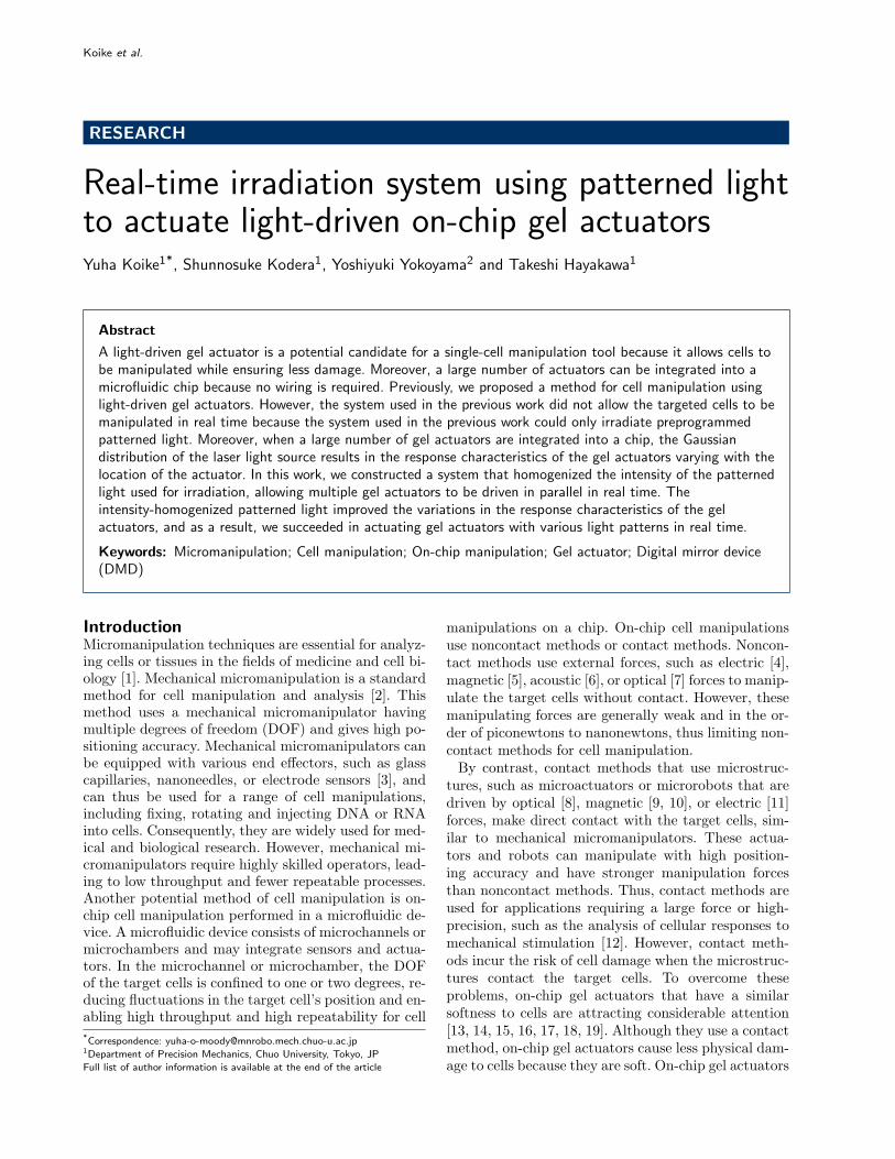
Figure 1 Concept of the proposed on-chip gel actuator. (a) Light drive for the gel actuator (b) Concept of the irradiation system ofpatterned light using a digital micromirror device
are commonly made of poly(N-isopropylacrylamide)(PNIPAAm), a thermoresponsive hydrogel [20]. PNI-PAAm swells in water when its temperature is lessthan the lower critical solution temperature (LCST)(≤32◦C) and shrinks when its temperature is higherthan the LCST (≥32◦C). Thus, by controlling thetemperature of the PNIPAAm, we can use this vol-ume change as an actuator. Previously, we proposeda method for driving an on-chip gel actuator madeof PNIPAAm using light irradiation [18, 19]. In thismethod, gel actuators are fabricated on a glass sub-strate with a light-absorbing pattern. On irradiatingthe light absorber with light, the temperature of thelight absorber increases and the gel actuators shrink,as shown in Fig. 1 (a). In our previous work[18, 19],we succeeded in integrating a large number of gel ac-tuators into a microfluidic chip and driving multipleactuators by irradiating the integrated gel actuatorswith patterned light. Additionally, we used the inte-grated gel actuators to demonstrate various cell ma-nipulations, including cell transporting, trapping andsorting. However, it was difficult to manipulate thetargeted cells with arbitrary timings because the pre-vious system could only irradiate the gel with pre-programmed light patterns. Moreover, the irradiatedlight had an intensity distribution of Gaussian distri-bution in a workspace of the manipulation. Therefore,when numerous gel actuators were integrated into amicrofluidic chip, shrink responses of the actuatorswere different and it was difficult to control actua-tion timings of actuators. In this paper, we describethe construction of a system for generating light pat-terns in real time and homogenizing the intensity ofthe light. We evaluate the switching responses of the
irradiated light and the homogeneity of the patternedlight. Finally, we confirm that patterned gel actuatorscan be actuated with approximately the same responsetimes and actuated with various light patterns in realtime.
ConceptFig. 1 (b) presents the conceptual diagram of a systemthat uses a digital micromirror device (DMD) to drivemultiple gel actuators. First, the operator observes amicroscopic image on a control PC. Next, the operatorinputs coordinates or areas on the image using a mouseand keyboard to determine the light irradiation pointor area. Finally, the computer generates a patternedimage based on the input coordinates or area data andsends it to the DMD to generate irradiation with thepatterned light. This process runs at 30 fps in realtime, and the operator can switch the points or areasof light being irradiated in real time.
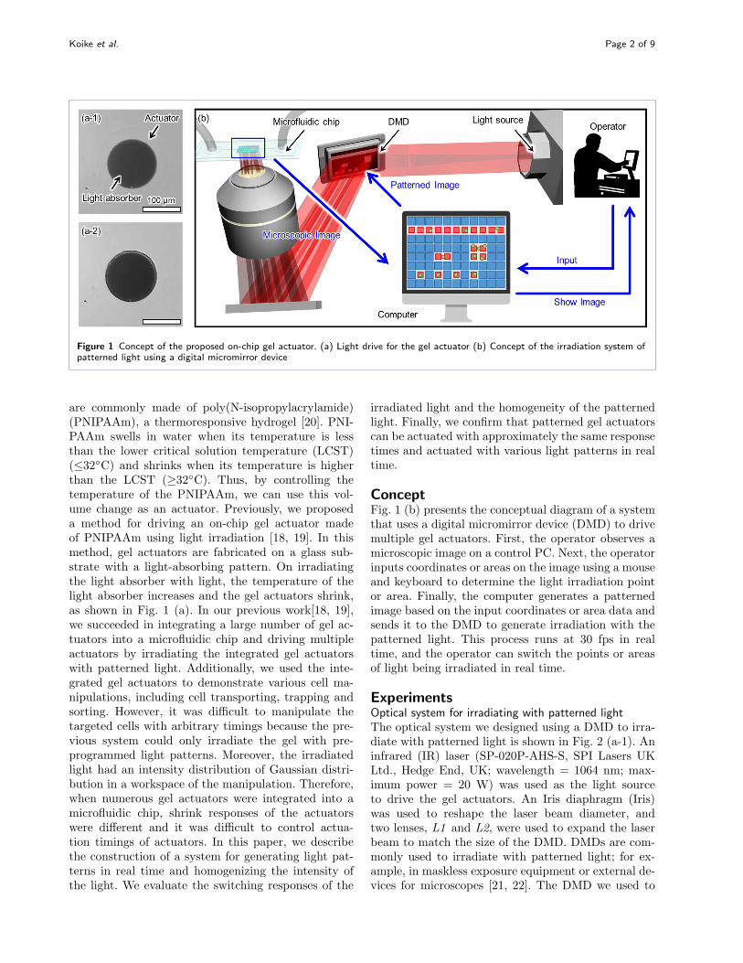
ExperimentsOptical system for irradiating with patterned lightThe optical system we designed using a DMD to irra-diate with patterned light is shown in Fig. 2 (a-1). Aninfrared (IR) laser (SP-020P-AHS-S, SPI Lasers UKLtd., Hedge End, UK; wavelength = 1064 nm; max-imum power = 20 W) was used as the light sourceto drive the gel actuators. An Iris diaphragm (Iris)was used to reshape the laser beam diameter, andtwo lenses, L1 and L2, were used to expand the laserbeam to match the size of the DMD. DMDs are com-monly used to irradiate with patterned light; for ex-ample, in maskless exposure equipment or external de-vices for microscopes [21, 22]. The DMD we used to
Koike et al. Page 3 of 9
generate patterned light (LC4500-RGB-EKT, KeynotePhotonics, Texas, United States) had a resolution of912 x 1140 pixels. The patterned light generated bythe DMD irradiated the microfluidic device throughthree lenses: L3, L4 and an objective lens (LMPlan N10x/0.30 Na IR, Olympus, Tokyo, Japan). A dichroicmirror (86-694, Edmund Optics, Barrington, USA;cutoff wavelength = 950 nm) was used to reflect the IRlaser beam to observe the device with visible light. Mi-croscopic images were acquired using a complementarymetal oxide semiconductor (CMOS) camera (GS3-U3-23S6C-C, FLIR Systems Japan K.K., Tokyo, Japan).Usually, when visible light is focused on the focal planeof an objective lens, the IR laser beam is out of focusas a result of chromatic aberrations at different wave-lengths, as shown in Fig. 2 (a-2). To counter this, weused lenses L3 and L4 to focus both the visible lightand the IR laser beam onto the same focal plane (Fig.2 (a-3)). When L3 was moved closer to the DMD, thefocal point of the IR laser beam moved to the bot-tom side of the microfluidic device, and . when L3 wasmoved away from the DMD, the focal point of the IRlaser beam moved to the upper side of the microfluidicdevice. Fig. 2 (b) shows a photograph of the opticalsystem we constructed.
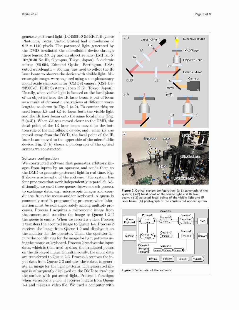
Software configurationWe constructed software that generates arbitrary im-ages from inputs by an operator and sends them tothe DMD to generate patterned light in real time. Fig.3 shows a schematic of the software. The system hasfour processes that work independently in parallel. Ad-ditionally, we used three queues between each processto exchange data; e.g., microscopic images and coor-dinates from the mouse and/or keyboard. A queue iscommonly used in programming processes when infor-mation must be exchanged safely among multiple pro-cesses. Process 1 acquires a microscopic image fromthe camera and transfers the image to Queue 1-2 ifthe queue is empty. When we record a video, Process1 transfers the acquired image to Queue 1-4. Process 2receives the image from Queue 1-2 and displays it onthe monitor for the operator. Then, the operator in-puts the coordinates for the image for light patterns us-ing the mouse or keyboard. Process 2 receives the inputdata, which is then used to draw the irradiated pointson the displayed image. Simultaneously, the input dataare transferred to Queue 2-3. Process 3 receives the in-put data from Queue 2-3 and uses these data to gener-ate an image for the light patterns. The generated im-age is subsequently displayed on the DMD to irradiatethe surface with patterned light. Process 4 functionswhen we record a video; it receives images from Queue1-4 and makes a video file. We used a computer with
Figure 2 Optical system configuration: (a-1) schematic of thesystem; (a-2) focal point of the visible light and IR laserbeam; (a-3) adjusted focal points of the visible light and IRlaser beam; (b) photograph of the constructed optical system
Figure 3 Schematic of the software
Koike et al. Page 4 of 9
an Intel core i7-8700 processor (6 physical cores, 3.20GHz), 64 GB of DDR4 memory and the Windows 10operating system. The software was developed usingPython 3.6.8 .
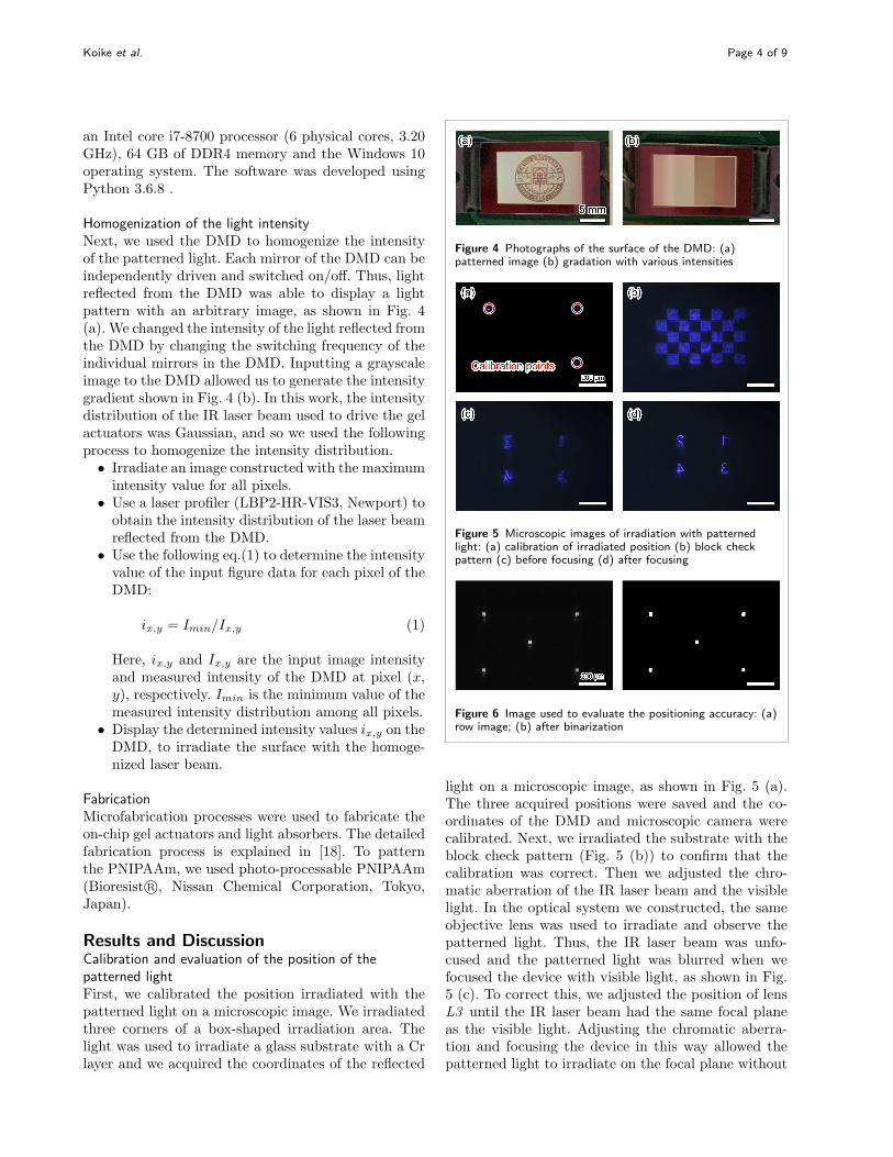
Homogenization of the light intensityNext, we used the DMD to homogenize the intensityof the patterned light. Each mirror of the DMD can beindependently driven and switched on/off. Thus, lightreflected from the DMD was able to display a lightpattern with an arbitrary image, as shown in Fig. 4(a). We changed the intensity of the light reflected fromthe DMD by changing the switching frequency of theindividual mirrors in the DMD. Inputting a grayscaleimage to the DMD allowed us to generate the intensitygradient shown in Fig. 4 (b). In this work, the intensitydistribution of the IR laser beam used to drive the gelactuators was Gaussian, and so we used the followingprocess to homogenize the intensity distribution.• Irradiate an image constructed with the maximumintensity value for all pixels.
• Use a laser profiler (LBP2-HR-VIS3, Newport) toobtain the intensity distribution of the laser beamreflected from the DMD.
• Use the following eq.(1) to determine the intensityvalue of the input figure data for each pixel of theDMD:
ix,y = Imin/Ix,y (1)
Here, ix,y and Ix,y are the input image intensityand measured intensity of the DMD at pixel (x,y), respectively. Imin is the minimum value of themeasured intensity distribution among all pixels.
• Display the determined intensity values ix,y on theDMD, to irradiate the surface with the homoge-nized laser beam.
FabricationMicrofabrication processes were used to fabricate theon-chip gel actuators and light absorbers. The detailedfabrication process is explained in [18]. To patternthe PNIPAAm, we used photo-processable PNIPAAm(Bioresist R©, Nissan Chemical Corporation, Tokyo,Japan).
Results and DiscussionCalibration and evaluation of the position of thepatterned lightFirst, we calibrated the position irradiated with thepatterned light on a microscopic image. We irradiatedthree corners of a box-shaped irradiation area. Thelight was used to irradiate a glass substrate with a Crlayer and we acquired the coordinates of the reflected
Figure 4 Photographs of the surface of the DMD: (a)patterned image (b) gradation with various intensities
Figure 5 Microscopic images of irradiation with patternedlight: (a) calibration of irradiated position (b) block checkpattern (c) before focusing (d) after focusing
Figure 6 Image used to evaluate the positioning accuracy: (a)row image; (b) after binarization
light on a microscopic image, as shown in Fig. 5 (a).The three acquired positions were saved and the co-ordinates of the DMD and microscopic camera werecalibrated. Next, we irradiated the substrate with theblock check pattern (Fig. 5 (b)) to confirm that thecalibration was correct. Then we adjusted the chro-matic aberration of the IR laser beam and the visiblelight. In the optical system we constructed, the sameobjective lens was used to irradiate and observe thepatterned light. Thus, the IR laser beam was unfo-cused and the patterned light was blurred when wefocused the device with visible light, as shown in Fig.5 (c). To correct this, we adjusted the position of lensL3 until the IR laser beam had the same focal planeas the visible light. Adjusting the chromatic aberra-tion and focusing the device in this way allowed thepatterned light to irradiate on the focal plane without
Koike et al. Page 5 of 9
blurring, as shown in Fig. 5 (d). Finally, we used thefollowing process to evaluate the positioning accuracyof the irradiated points.
• Irradiate the square shape with a side length of 30µm to four corners and center of the irradiationarea (Fig. 6 (a)) and capture the image.
• Process the binarization of the captured image(Fig. 6 (b)).
• Calculate the center of each irradiation area.• Compare the acquired center of the area and theinput values.
The maximum difference in positions of the irradi-ated point was approximately 3.5 µm, and the averagedifference was 2.1 µm. These values are thought to besmall enough to manipulate biological cells of a size ofapproximately 10-20 µm.
Resolution of the generated light pattern
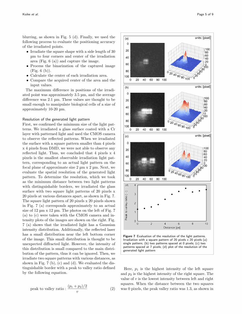
First, we confirmed the minimum size of the light pat-terns. We irradiated a glass surface coated with a Crlayer with patterned light and used the CMOS camerato observe the reflected patterns. When we irradiatedthe surface with a square pattern smaller than 4 pixelsx 4 pixels from DMD, we were not able to observe anyreflected light. Thus, we concluded that 4 pixels x 4pixels is the smallest observable irradiation light pat-tern, corresponding to an actual light pattern on thefocal plane of approximate size 2 µm x 2 µm. Next, weevaluate the spatial resolution of the generated lightpattern. To determine the resolution, which we tookas the minimum distance between two light patternswith distinguishable borders, we irradiated the glasssurface with two square light patterns of 20 pixels x20 pixels at various distances apart, as shown in Fig. 7.The square light pattern of 20 pixels x 20 pixels shownin Fig. 7 (a) corresponds approximately to an actualsize of 12 µm x 12 µm. The photos on the left of Fig. 7(a) to (c) were taken with the CMOS camera and in-tensity plots of the images are shown on the right. Fig.7 (a) shows that the irradiated light has a Gaussianintensity distribution. Additionally, the reflected laserhas a small distribution near the left bottom cornerof the image. This small distribution is thought to beunexpected diffracted light. However, the intensity ofthis distribution is small compared to the main distri-bution of the pattern, thus it can be ignored. Then, weirradiate two square patterns with various distances, asshown in Fig. 7 (b), (c) and (d). We evaluated the dis-tinguishable border with a peak to valley ratio definedby the following equation.
peak to valley ratio :(p1 + p2)/2
v(2)
Figure 7 Evaluation of the resolution of the light patterns.Irradiation with a square pattern of 20 pixels x 20 pixels (a)single pattern; (b) two patterns spaced at 0 pixels; (c) twopatterns spaced at 7 pixels; (d) plot of the resolution of thegenerated light pattern
Here, p1 is the highest intensity of the left square
and p2 is the highest intensity of the right square. The
value of v is the lowest intensity between left and right
squares. When the distance between the two squares
was 0 pixels, the peak valley ratio was 1.3, as shown in
Koike et al. Page 6 of 9
Fig. 7 (b) and (d). When the distance between the twosquares was 7 pixels, the peak to valley ratio became3.6, as shown in Fig. 7 (c) and (d). The value of thepeak to valley ratio saturated at around 3.3 to 3.6,as shown in Fig. 7 (d). From this, we determined theresolution of the patterned light to be approximately7 pixels, which corresponds to an actual distance of 4µm on the focal plane of the microscope. This value isthought to be small enough to manipulate biologicalcells of a size of approximately 10-20 µm.
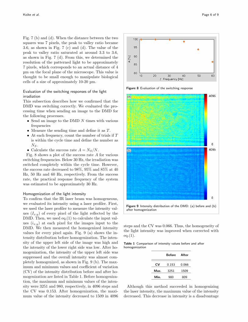
Evaluation of the switching responses of the lightirradiationThis subsection describes how we confirmed that theDMD was switching correctly. We evaluated the pro-cessing time when sending an image to the DMD forthe following processes.• Send an image to the DMD N times with variousfrequencies
• Measure the sending time and define it as T .• At each frequency, count the number of trials if Tis within the cycle time and define the number asNS .
• Calculate the success rate A = NS/N .Fig. 8 shows a plot of the success rate A for various
switching frequencies. Below 30 Hz, the irradiation wasswitched completely within the cycle time. However,the success rate decreased to 98%, 95% and 85% at 40Hz, 50 Hz and 60 Hz, respectively. From the successrate, the practical response frequency of the systemwas estimated to be approximately 30 Hz.
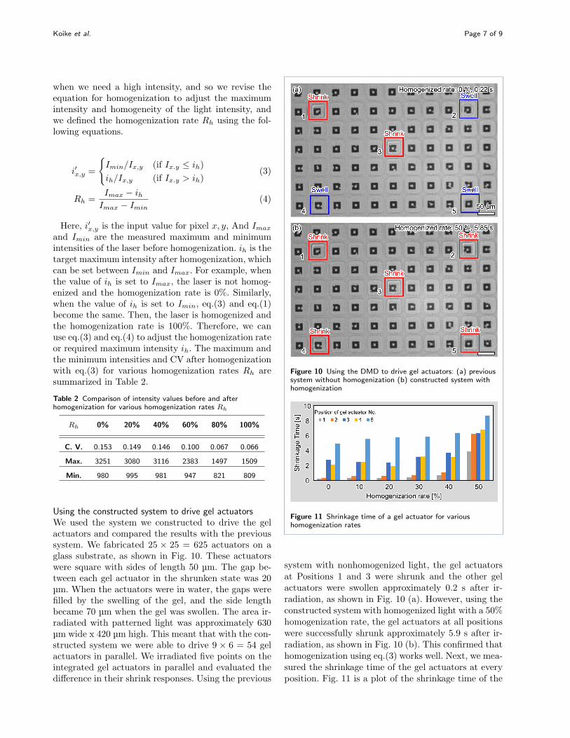
Homogenization of the light intensityTo confirm that the IR laser beam was homogeneous,we evaluated its intensity using a laser profiler. First,we used the laser profiler to measure the intensity val-ues (Ix,y) of every pixel of the light reflected by theDMD. Then, we used eq.(1) to calculate the input val-ues (ix,y) at each pixel for the images input to theDMD. We then measured the homogenized intensityvalues for every pixel again. Fig. 9 (a) shows the in-tensity distribution before homogenization. The inten-sity of the upper left side of the image was high andthe intensity of the lower right side was low. After ho-mogenization, the intensity of the upper left side wassuppressed and the overall intensity was almost com-pletely homogenized, as shown in Fig. 9 (b). The max-imum and minimum values and coefficient of variation(CV) of the intensity distribution before and after ho-mogenization are listed in Table 1. Before homogeniza-tion, the maximum and minimum values of the inten-sity were 3251 and 980, respectively, in 4096 steps andthe CV was 0.153. After homogenization, the maxi-mum value of the intensity decreased to 1509 in 4096
Figure 8 Evaluation of the switching response
Figure 9 Intensity distribution of the DMD: (a) before and (b)after homogenization
steps and the CV was 0.066. Thus, the homogeneity ofthe light intensity was improved when corrected witheq.(1).
Table 1 Comparison of intensity values before and afterhomogenization
Before After
CV 0.153 0.066
Max. 3251 1509
Min. 980 809
Although this method succeeded in homogenizingthe laser intensity, the maximum value of the intensitydecreased. This decrease in intensity is a disadvantage
Koike et al. Page 7 of 9
when we need a high intensity, and so we revise theequation for homogenization to adjust the maximumintensity and homogeneity of the light intensity, andwe defined the homogenization rate Rh using the fol-lowing equations.
i′x,y =
{
Imin/Ix,y (if Ix.y ≤ ih)
ih/Ix,y (if Ix.y > ih)(3)
Rh =Imax − ih
Imax − Imin
(4)
Here, i′x,y is the input value for pixel x, y, And Imax
and Imin are the measured maximum and minimumintensities of the laser before homogenization. ih is thetarget maximum intensity after homogenization, whichcan be set between Imin and Imax. For example, whenthe value of ih is set to Imax, the laser is not homog-enized and the homogenization rate is 0%. Similarly,when the value of ih is set to Imin, eq.(3) and eq.(1)become the same. Then, the laser is homogenized andthe homogenization rate is 100%. Therefore, we canuse eq.(3) and eq.(4) to adjust the homogenization rateor required maximum intensity ih. The maximum andthe minimum intensities and CV after homogenizationwith eq.(3) for various homogenization rates Rh aresummarized in Table 2.
Table 2 Comparison of intensity values before and afterhomogenization for various homogenization rates Rh
Rh 0% 20% 40% 60% 80% 100%
C. V. 0.153 0.149 0.146 0.100 0.067 0.066
Max. 3251 3080 3116 2383 1497 1509
Min. 980 995 981 947 821 809
Using the constructed system to drive gel actuatorsWe used the system we constructed to drive the gelactuators and compared the results with the previoussystem. We fabricated 25 × 25 = 625 actuators on aglass substrate, as shown in Fig. 10. These actuatorswere square with sides of length 50 µm. The gap be-tween each gel actuator in the shrunken state was 20µm. When the actuators were in water, the gaps werefilled by the swelling of the gel, and the side lengthbecame 70 µm when the gel was swollen. The area ir-radiated with patterned light was approximately 630µm wide x 420 µm high. This meant that with the con-structed system we were able to drive 9 × 6 = 54 gelactuators in parallel. We irradiated five points on theintegrated gel actuators in parallel and evaluated thedifference in their shrink responses. Using the previous
Figure 10 Using the DMD to drive gel actuators: (a) previoussystem without homogenization (b) constructed system withhomogenization
Figure 11 Shrinkage time of a gel actuator for varioushomogenization rates
system with nonhomogenized light, the gel actuatorsat Positions 1 and 3 were shrunk and the other gelactuators were swollen approximately 0.2 s after ir-radiation, as shown in Fig. 10 (a). However, using theconstructed system with homogenized light with a 50%homogenization rate, the gel actuators at all positionswere successfully shrunk approximately 5.9 s after ir-radiation, as shown in Fig. 10 (b). This confirmed thathomogenization using eq.(3) works well. Next, we mea-sured the shrinkage time of the gel actuators at everyposition. Fig. 11 is a plot of the shrinkage time of the
Koike et al. Page 8 of 9
gel actuators for various homogenization rates. The ex-periment was conducted with a homogenization rateof 50% or less. These results highlight the large dif-ference between the shrinkage times of the individualactuators before homogenization. After homogeniza-tion, the shrinkage times of actuators 1, 2, and 4 werealmost the same. The CVs of the shrinkage times ateach homogenization rate are listed in Table 3. For a0% homogenization rate, the CV was 0.83. For a 50%homogenization rate, the CV was 0.24. This confirmedthat homogenizing the laser beam reduces the varia-tion in the shrinkage times of the gel actuators.
Table 3 Comparison of shrinkage times for differenthomogenization rates
Homogenization rate Rh
0 % 10 % 20 % 30 % 40 % 50 %
C. V. 0.83 0.82 0.88 0.73 0.67 0.24
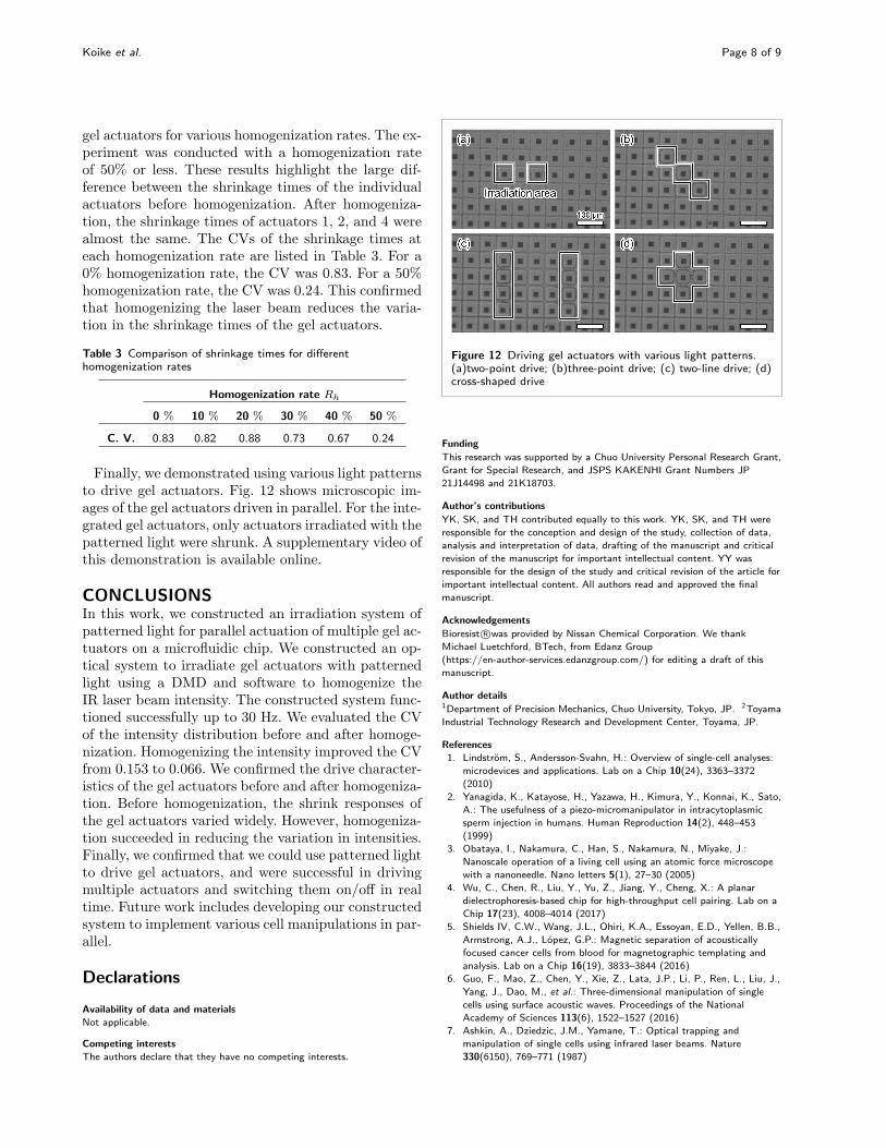
Finally, we demonstrated using various light patternsto drive gel actuators. Fig. 12 shows microscopic im-ages of the gel actuators driven in parallel. For the inte-grated gel actuators, only actuators irradiated with thepatterned light were shrunk. A supplementary video ofthis demonstration is available online.
CONCLUSIONSIn this work, we constructed an irradiation system ofpatterned light for parallel actuation of multiple gel ac-tuators on a microfluidic chip. We constructed an op-tical system to irradiate gel actuators with patternedlight using a DMD and software to homogenize theIR laser beam intensity. The constructed system func-tioned successfully up to 30 Hz. We evaluated the CVof the intensity distribution before and after homoge-nization. Homogenizing the intensity improved the CVfrom 0.153 to 0.066. We confirmed the drive character-istics of the gel actuators before and after homogeniza-tion. Before homogenization, the shrink responses ofthe gel actuators varied widely. However, homogeniza-tion succeeded in reducing the variation in intensities.Finally, we confirmed that we could use patterned lightto drive gel actuators, and were successful in drivingmultiple actuators and switching them on/off in realtime. Future work includes developing our constructedsystem to implement various cell manipulations in par-allel.
Declarations
Availability of data and materials
Not applicable.
Competing interests
The authors declare that they have no competing interests.
Figure 12 Driving gel actuators with various light patterns.(a)two-point drive; (b)three-point drive; (c) two-line drive; (d)cross-shaped drive
Funding
This research was supported by a Chuo University Personal Research Grant,
Grant for Special Research, and JSPS KAKENHI Grant Numbers JP
21J14498 and 21K18703.
Author’s contributions
YK, SK, and TH contributed equally to this work. YK, SK, and TH were
responsible for the conception and design of the study, collection of data,
analysis and interpretation of data, drafting of the manuscript and critical
revision of the manuscript for important intellectual content. YY was
responsible for the design of the study and critical revision of the article for
important intellectual content. All authors read and approved the final
manuscript.
Acknowledgements
Bioresist R©was provided by Nissan Chemical Corporation. We thank
Michael Luetchford, BTech, from Edanz Group
(https://en-author-services.edanzgroup.com/) for editing a draft of this
manuscript.
Author details1Department of Precision Mechanics, Chuo University, Tokyo, JP. 2Toyama
Industrial Technology Research and Development Center, Toyama, JP.
References
1. Lindstrom, S., Andersson-Svahn, H.: Overview of single-cell analyses:
microdevices and applications. Lab on a Chip 10(24), 3363–3372
(2010)
2. Yanagida, K., Katayose, H., Yazawa, H., Kimura, Y., Konnai, K., Sato,
A.: The usefulness of a piezo-micromanipulator in intracytoplasmic
sperm injection in humans. Human Reproduction 14(2), 448–453
(1999)
3. Obataya, I., Nakamura, C., Han, S., Nakamura, N., Miyake, J.:
Nanoscale operation of a living cell using an atomic force microscope
with a nanoneedle. Nano letters 5(1), 27–30 (2005)
4. Wu, C., Chen, R., Liu, Y., Yu, Z., Jiang, Y., Cheng, X.: A planar
dielectrophoresis-based chip for high-throughput cell pairing. Lab on a
Chip 17(23), 4008–4014 (2017)
5. Shields IV, C.W., Wang, J.L., Ohiri, K.A., Essoyan, E.D., Yellen, B.B.,
Armstrong, A.J., Lopez, G.P.: Magnetic separation of acoustically
focused cancer cells from blood for magnetographic templating and
analysis. Lab on a Chip 16(19), 3833–3844 (2016)
6. Guo, F., Mao, Z., Chen, Y., Xie, Z., Lata, J.P., Li, P., Ren, L., Liu, J.,
Yang, J., Dao, M., et al.: Three-dimensional manipulation of single
cells using surface acoustic waves. Proceedings of the National
Academy of Sciences 113(6), 1522–1527 (2016)
7. Ashkin, A., Dziedzic, J.M., Yamane, T.: Optical trapping and
manipulation of single cells using infrared laser beams. Nature
330(6150), 769–771 (1987)
Koike et al. Page 9 of 9
8. Onda, K., Arai, F.: Multi-beam bilateral teleoperation of holographic
optical tweezers. Optics express 20(4), 3633–3641 (2012)
9. Sakuma, S., Yamanishi, Y., Arai, F.: Magnetically driven microtools
actuated by a focused magnetic field for separating of microparticles.
Journal of Robotics and Mechatronics 21(2), 209 (2009)
10. Hagiwara, M., Kawahara, T., Yamanishi, Y., Masuda, T., Feng, L.,
Arai, F.: On-chip magnetically actuated robot with ultrasonic vibration
for single cell manipulations. Lab on a Chip 11(12), 2049–2054 (2011)
11. Ito, K., Sakuma, S., Kimura, M., Takebe, T., Kaneko, M., Arai, F.:
Temporal transition of mechanical characteristics of huvec/msc
spheroids using a microfluidic chip with force sensor probes.
Micromachines 7(12), 221 (2016)
12. Park, K., Mehrnezhad, A., Corbin, E.A., Bashir, R.: Optomechanical
measurement of the stiffness of single adherent cells. Lab on a Chip
15(17), 3460–3464 (2015)
13. Ichikawa, A., Arai, F., Yoshikawa, K., Uchida, T., Fukuda, T.: In situ
formation of a gel microbead for indirect laser micromanipulation of
microorganisms. Applied Physics Letters 87(19), 191108 (2005)
14. Ito, K., Sakuma, S., Yokoyama, Y., Arai, F.: On-chip gel-valve using
photoprocessable thermoresponsive gel. ROBOMECH Journal 1(1),
1–8 (2014)
15. Hayakawa, T., Sakuma, S., Fukuhara, T., Yokoyama, Y., Arai, F.: A
single cell extraction chip using vibration-induced whirling flow and a
thermo-responsive gel pattern. Micromachines 5(3), 681–696 (2014)
16. d’Eramo, L., Chollet, B., Leman, M., Martwong, E., Li, M., Geisler,
H., Dupire, J., Kerdraon, M., Vergne, C., Monti, F., et al.: Microfluidic
actuators based on temperature-responsive hydrogels. Microsystems &
Nanoengineering 4(1), 1–7 (2018)
17. Lee, W., Kalashnikov, N., Mok, S., Halaoui, R., Kuzmin, E., Putnam,
A.J., Takayama, S., Park, M., McCaffrey, L., Zhao, R., et al.:
Dispersible hydrogel force sensors reveal patterns of solid mechanical
stress in multicellular spheroid cultures. Nature communications 10(1),
1–14 (2019)
18. Koike, Y., Yokoyama, Y., Hayakawa, T.: Light-driven hydrogel
microactuators for on-chip cell manipulations. Frontiers in Mechanical
Engineering 6, 2 (2020)
19. Wada, H., Koike, Y., Yokoyama, Y., Hayakawa, T.: Evaluation of the
response characteristics of on-chip gel actuators for various single cell
manipulations. IEEE Robotics and Automation Letters 5(4),
5205–5212 (2020)
20. Yokoyama, Y., Umezaki, M., Kishimura, T., Tamiya, E., Takamura, Y.:
Micro-and nano-fabrication of stimulus-responsive polymer using
nanoimprint lithography. Journal of Photopolymer Science and
Technology 24(1), 63–70 (2011)
21. Tompkins, N., Fraden, S.: An inexpensive programmable illumination
microscope with active feedback. American journal of physics 84(2),
150–158 (2016)
22. Steyrer, B., Busetti, B., Harakaly, G., Liska, R., Stampfl, J.: Hot
lithography vs. room temperature dlp 3d-printing of a dimethacrylate.
Additive Manufacturing 21, 209–214 (2018)

Supplementary Files
This is a list of supplementary �les associated with this preprint. Click to download.
supplementaryv2.1.mp4