radio over fiber for 3g cellular system · patil college of engineering, akurdi, pune for their...
TRANSCRIPT

Master thesis
On
Radio over fiber for 3G cellular System
Submitted to
Shivaji University, Kolhapur
Prepared By
Mr. Saurabh Rai Dhirendra Prasad
Under the guidance of
Prof P. P. Kulkarni
M.E. (Electronics & Telecommunication)
Department of Electronics Engineering,
K. I. T's College of Engineering, Kolhapur
2009-2010

Department of Electronics Engineering,
K. I. T's College of Engineering, Kolhapur
Certificate
This is to certify that Mr. Saurabh R. Prasad has prepared the project report on "Radio over Fiber for 3G Cellular System" under my guidance and supervision in a satisfactory manner for the partial fulfillment of M.E. (Electronics & Telecommunication, Sem-IV) as per the rules and regulations of the Shivaji University, Kolhapur for the year 2009-2010.
Date -
Place - Kolhapur
Examiners
Internal -
External -
H. O. D.
Prof. A. R. Nigavekar
Guide
Prof P. P. Kulkarni
Principal


ACKNOWLEDGEMENT
Radio over Fiber (RoF) technology is a technology that essentially integrates two worlds- the radio world and the optic world. Thus in this integrated world, one has to face with double share of problems. Stepping into this field in my early stage of research work, I encountered many hurdles and challenges along the way. However with the help and contributions of many people, I could be able to realize working of RoF system from a mere idea. My research work over the RoF technology is really an enlightening and satisfying experience. Therefore it gives me great pleasure to acknowledge and thank many people who contributed in various ways for the successful completion of this research work.
Words are inadequate to express my feelings while recording my deep sense of gratitude and respect to my guide Prof (Mrs) P. P. Kulkarni. The work presented here could not have been accomplished without her inspiring guidance, constructive criticism and sustained encouragement during the course of my research work. This research work has been carried out under the direct supervision and leadership of Prof A. R. Nigwekar, Head of the department, without whose supervision and support it was merely impossible to accomplish the task. I thank them for meticulous manner in which my thesis was reviewed which greatly improved its quality. I am very grateful for many discussions we had, especially on analysis of the theoretical and experimental results.
I offer my humble and sincere thanks to Dr. R. A. Raikar, Principal, KIT’s College of Engineering, Kolhapur for his all possible cooperation. I express my sincere thanks to Prof (Dr) A. S. Vaingankar, Prof. (Mrs) M. R. Dixit, Prof Y. M. Patil, Prof N. B. Sambhare, Prof V. K. Desai and all staff members from Electronics Department of K.I.T’s College of Engineering, Kolhapur for their keen interest and an encouragement during the research period.
I sincerely acknowledge Mr Nagnur from BSNL Kolhapur for doing all possible help during the course of research work like providing attenuator, power meter, patch cord, optic fiber cable and technical consultancy etc. I will also acknowledge Amphenol, Pune for solving connectivity constraint in the research work. Moreover I would like to pay my thanks personally to Defence Institute of Advanced Technology (DIAT), Pune for their necessary helps.
It gives me immense pleasure to express my heartfelt thanks to my dearest friends Mandar Sontakke, Tejshree Mohite, Pravin Kothawale, Vijaya Kamble, Prof S. G. Patil, Kishori Naik and Milind Patil for their memorable help and co-operation and so many friends who helped me directly or indirectly during this work.

I place on record my deep sense of gratitude to Col S. K. Joshi, Director, D. Y. Patil Pratishthan, Akurdi complex, Dr. A. A. Ghatol, Technical Advisor to D. Y. Patil Pratisthan, Dr (Mrs) Prachi Warnekar, Principal, D. Y. Patil College of Engineering, Akurdi, Pune, Mrs A. V. Patil, Head of the E & TC Department, D. Y. Patil College of Engineering, Akurdi, Pune for their valuable advice and encouragement, and all possible help from administration point of view. At the verge of completion of this research work I can not forget Dr P. J. Kulkarni, Head of the CSE Department, WCE Sangli from whom I could learn to endeavor for achieving the excellence and Dr A. I. Wasif, Principal D. K. T. E Textile and Engineering Institute, Ichalkaranji from whom I could learn honesty towards the work. At this moment I can not forget Dr J. V. Desai, Vice Principal, TEI, Ichalkaranji who brought me in the noble field of teaching.
I take this moment to bow in front of my father Dr. Rai Dhirendra Prasad, mother Nirmala Prasad whose blessing have been my inspiration to complete this work. My deepest thanks and appreciations are reserved for my dear brother Neeraj and sister Deepika.
At this moment on behalf of me and my batch I pay my tributes to our dearest friend Late Mr Atul Kulkarni whom we lost forever.
Place: Kolhapur Saurabh R. Prasad
Date: 19th October 2009

Contents
• Acknowledgement i
• Table of Contents iii
• Synopsis iv
• List of figures xiv
• List of abbreviations xvi
1. Introduction to Wireless World 1
2. The Concept of Radio over Fiber 10
3. The Different Characteristics of the Optical Fiber Link 18
4. Laser Diode and Detector 29
5. The Different Techniques for Transporting RF Signals over OFC 52
6. The Experimental Set-Up 63
7. Observations 75
8. Results and Discussion 87
9. Conclusion and Future Scope 95
10. Summary of Publication 100
11. References 102


KIT’s
College of Engineering, Kolhapur
Department of Electronics and Telecommunication Engineering
Synopsis for M.E. (EXTC) Dissertation
1. Name of the College: KIT’s College of Engineering, Kolhapur
2. Name of the Course: M.E. (Electronics and Telecommunication)
3. Name of the Candidate: Mr. S. R. Prasad
4. Month of Registration: July 2007
5 Name of the guide: Prof. Mrs. P. P. Kulkarni
6. Name of the co-guide: Prof. A. R. Nigvekar
7. Proposed title of Dissertation: “Radio over fiber for 3G Cellular System”
Relevance:

To meet the explosive demands of high capacity and broadband wireless access, modern cell based wireless networks have the trend to increase the number of cells by the process called as cell splitting and utilization of higher frequency bands. It leads to a large number of base stations to be deployed. In such cases the radio over fiber technique provides functionally simple base stations that are interconnected to a central control station via an optical fiber. This allows reduction in system cost. Radio over fiber is an analog optical link transmitting optical carrier modulated by the radio frequency signal. This technique facilitates to transmit radio frequency signal through the optical fiber in downlink that is from mobile terminal to base station and base station to central station and also in uplink that is from central station to the base station and from base station to the mobile terminal. In our project we are concerned with the WCDMA signal transmission through radio over fiber communication link and evaluate its performance.
Traditionally the signal is transmitted via fiber by using baseband digital modulation. In this technique, optical source is turned on and off by digital data input ‘1’ and ‘0’. Thus optical carrier is modulated. This method suffers from few drawbacks. One drawback is that this method requires fast analog to digital converter at the transmitter side to convert analog signal into digital form and fast digital to analog converter at the receiver side to convert digital signal to original analog form. These fast analog to digital converters and digital to analog converters are costly and hence overall system is not cost effective. Thus in the radio over fiber technique we can replace the digital modulation of optical carrier by analog modulation where radio frequency signal modulates the optical carrier. There are two types of this analog modulation. The first type is called as direct intensity modulation where the radio frequency signal is directly superimposed on the dc bias current, which drives the optical source, for example laser diode. Here the intensity of light emitted by the laser diode varies in accordance with the radio frequency signal. But this direct modulation method suffers from few disadvantages such as frequency chirping and cause non-linearity in the output. Thus in our project we are using second type of laser modulation by radio frequency signal, which is called as electro absorption modulation. In this method the intensity of the laser beam does not vary directly but the intensity of the semiconductor material, which follows the laser diode varies in accordance with the radio frequency signal. Thus in either type of the analog modulation we can eliminate the need to convert analog signal to digital form. This technique of analog modulation is called as the radio over fiber.
In radio over fiber, the spectrum inside the fiber consists of both the optical carrier and radio frequency sub carrier. Also the fiber optic cable possesses inherent property of enormous bandwidth. Hence the analog optical link can transmit radio waves upto tens of GHz. Therefore multiple radio frequency sub-carriers can be summed together and used to modulate a single optical carrier. In addition, new techniques such as fiber Bragg grating enable radio frequency signal to be filtered and tuned optically. This makes radio over fiber approach more attractive and open new opportunities.
Present Theories and Practices:

Recently ‘wireless last mile’ has received considerable attention since it requires much less infrastructure as compared to wire line alternatives such as digital subscriber line (DSL) and cable modem.
In traditional wireless delivery system based on optical network, baseband radio signals from central station to the base station are carried by the fiber. At the base station, these radio signals are up converted to the operating radio frequency and transmitted to the subscriber.
In radio over fiber delivery system, the actual radio signals are transported over the optical fiber thus up conversion at the base station is not required and the costly radio frequency conversion equipments are eliminated.
The radio frequency link consists of three main elements.
1. An optical source (laser) with RF-Optical modulating arrangement.2. A single mode fiber link3. An optical receiver with a band pass filter to recover the original signal
The basic experimental set up for radio over fiber is given as below.
Semiconductor laser: Although there are numerous types of lasers that are used as light sources, here we choose the high-speed semiconductor laser that could be coupled with optical fiber. Even under this category, there are two types of laser that are mainly used for analog modulation.
1. Fabry-Perot Laser2. Distributed Feedback Laser (DFB)
Fabry Perot Laser: This laser reflection from the laser facets to provide necessary lasing. Though it has narrow line width, which indicates single mode operation, this laser has many longitudinal modes. This gives a wider line width, which causes more dispersion. Also this laser demonstrates a phenomenon

called as ‘mode hopping’ in which the power constantly shifts between different modes. Therefore, this laser is subjected to both, mode hopping and partition noise. Hence this laser is not regarded as a good optical source.
Distributed Feedback Laser (DFB): This laser uses distributed Bragg diffraction grating rather than cleaved mirror. Due to this special grating pattern, only one lasing mode is constructively created. Thus, this laser is essentially a single mode laser and subjected to less dispersion. Also it provides more dynamic range and the emission is relatively less distorted. Hence this laser has won popularity for analog applications like radio over fiber.
Dedicated indoor radio system can provide better coverage and capacity in public areas such as
airports, hotels and shopping malls, in addition to office buildings. The importance of indoor cellular
network increases when third generation radio systems are introduced, which gives user higher bit
rate with multimedia services. For example, wideband code division multiple access (WCDMA)
provides data rate upto 2Mbps, but at the expense of the decreased cell radius.
Radio over fiber technique can be used in Distributed Antenna System (DAS). In distributed antenna
system, a central station, also called as base station, feed many remote antenna units (RAUs)
through coaxial cable link. Using these schematics, the entire signal processing capabilities like
frequency up-conversion, carrier modulation, multiplexing etc are provided in central station so that
base RAU design is simple and inexpensive. This technique has the advantage of decoupling
coverage from capacity. Today 80-90% of all in-building DAS installations for cellular radio system
use passive coaxial cable distribution network. The main reason for this is the cost of fiber optics,
which is in general cost effective only for link spans longer than 100-200m. Cost is a major obstacle
to a more widespread implementation of fiber optic DAS. We can replace the coaxial cable
distribution network by the fiber optic cable distribution network using radio over fiber technology.
By doing so, RAUs are simplified significantly, as they need to do only opto-electric conversion and
amplification function. The centralization of radio signal processing function enables equipment
sharing. The DAS system using RoF is shown diagrammatically in the following figure.

The requirements on these RAUs are that they should be small, light, inexpensive and flexible
enough to act as a transceiver for all today’s wireless communication systems, and those of the
future. Low cost technologies that can be used include VCSELs and multimode fiber. However one
promising candidate providing these features is the electro-absorption transceiver (EAT). This
concept takes RAU simplification to the limit since only two components are required, an EAT and an
antenna. The EAT is a single device which is capable of functioning as a passive transceiver requiring
no amplifier or power supply. It acts as a photo-detector as a downlink path and as an optical
modulator for the uplink path. The lack of amplification places a strict limit on the radio coverage.
While shifting from conventional fiber optic wireless communication to radio over fiber based fiber optic wireless communication, we have to face few challenges as under.
Consider radio over fiber based wireless local area network operating at 2.4GHz band, which can provide high capacity wireless access. However due to high propagation and penetration loss in this frequency band, a typical room in the building must be surrounded by atleast one base station. As a result numerous base stations are required to cover the building. In such an environment, a slight movement of mobile host could trigger handoff which is quite difficult situation compared to traditional wireless local area network systems. Therefore it is obvious that handoff management becomes a significant issue.
Also radio over fiber based network architecture for road vehicle communication system (RVC) at millimeter wave band will be studied. In this case handoff management becomes even more difficult due to small cells and high user mobility.
Also radio over fiber based broadband wireless access network architecture for sparsely populated rural and remote areas can be studied. In this architecture a control station has optical tunable transmitter (TT) and tunable receiver pair (TR) and utilizes wavelength division multiplexing to access numerous antenna base station, each of which is fixed tuned to a wavelength for an efficient and flexible bandwidth allocation.
Quadrature modulators are used for reduction in the bandwidth for the given data rate. This is accomplished through modulating a carrier by two orthogonal data streams. If the phase and amplitude of two data streams are out of phase, then one of the sideband is completely cancelled out.
Theoretical Analysis and Proposed Methodology:
In radio over fiber, the microwave sub-carrier modulates the optical carrier. The microwave is
usually frequency modulated for wireless broadcasting. A conventional optical communication
system usually operates at the baseband with amplitude modulation. The interface of the two
systems thus needs an up conversion from baseband frequency to microwave frequency with AM to
FM transformation. An all-optical solution employs electro absorption laser module (EALM).
Experimental Set-up:

Given fig shows the experimental set-up used for radio signal transmission over fiber optic link. GC 5316 is a daughter cord, which generates WCDMA signal in the digital I/Q vector form. This I/Q vector is applied to PC-I through an interface GC 101. All the three PCs, which are PC-I, PC-II, and PC-III, are connected to local area network. Hence PC-II can get digital I/Q vector. PC-II applies this I/Q vector to TSW 3003. Inside TSW 3003, the I/Q vector modulates 2.4 GHz carrier frequency. Hence output of TSW 3003 is radio frequency. Thus we can say that TSW 3003 is responsible for the digital to analog conversion. This radio signal passes through coaxial cable and is then fed to 1550nm laser diode modulator. There happens electro absorption effect inside the laser diode modulator. This laser beam modulated by the radio frequency signal is passed through the fiber optic cable. Then at the receiving end, pin diode and low noise amplifier converts optical signal to the electrical form. This 2.4GHz electrical signal at the receiver is down converted to 2.4MHz. TSW 2100 applies clock signal to GC101. AFC8406 is a wide band amplifier, which converts 24.4MHz signal to I/Q vector, which is then applied, to PC-III.
By using the experimental set up shown above, we have proposed to measure the WCDMA signal quality. For this measurement a signal generator (Agilent E4436B or Rhode or Schwartz SMIQ) and a signal analyzer (Rhode and Schwartz FSIQ26) can be used. The different parameters which we can

measure include composite error vector magnitude (EVM), adjacent channel leakage ratio (ACLR) and peak code domain error (CDE). The EVM provides a way to quantify the errors in the digital demodulation and is sensitive to any signal impairment that affects the magnitude an phase of the demodulated signal. The ACLR is a measure of the power leakage from the main channel into adjacent ratio channel, where it can cause signal interference. The CDE specifies the limit for the error power in the code domain, and can address the possibility of uneven error power distribution. For the peak CDE analysis the signal is descrambled and de-spread in order to obtain the errors at the symbol level
The following points can be noted with regards to the radio over fiber.
1. In a radio over fiber system, a central office is connected t a remote base station by optical fiber, which carries the microwave sub-carriers. At the base station, the photo detectors recover the microwave signals.2. Radio over fiber has the advantage of centralizing the high-speed electronics in the central office and allowing effective long distance microwave transmission. Different semiconductor lasers used in radio over fiber technique include: directly modulated laser, optically injected laser and multisection laser.3. Microwave carrier is either frequency modulated or phase modulated. Amplitude modulation is not preferred because of high channel fading at microwave frequencies. In contrast, a conventional optical communication system employs baseband amplitude modulation because of its simplicity. Thus, when a conventional system is connected to radio over fiber system, an interface is required for baseband to microwave up conversion with simultaneous AM-to-FM transformation.4. Although this interface can be realized by electrically modulating radio over fiber light source by photo-detected signal of the baseband amplitude modulation, but a simple all optic method bypassing the electronics is preferred.
Implementation Tools
We can use various simulation software listed below.
1. Matlab2. Lab View
Expected Date of Completion: Dec 2008
Major equipments: 1. Lab Buddy: Discovery semiconductor USA
2. Laser Diode Module: Bookham, UK.
3. TI Evaluation Kits, USA
• TSW 3003 $ 500• GC5316• AFE8406• GC101
4. R&S Germany Spectrum Analyzer 3 GHz.
5. Single mode fiber 2KM
All above equipments are available with KITCOEK
Project Expenses (Approximately) = INR5000/- only

To the best of my knowledge and belief, the information given above is correct.
Signature of the student
(Mr. S. R. Prasad)
Signature of Guide Signature of HOD Signature of Principal
(Prof. Mrs. P. P. Kulkarni) (Prof. A.R. Nigvekar) (Prof. Dr. V.A. Raikar)
Signature of Co-Guide
(Prof. A. R. Nigvekar)
References:
1. S. Betti, A. Bizzotto, E. Brovi and M. Giaconi, “Effect of Semiconductor Laser Intrinsic Dynamic Distortion in Hybrid Fiber- CDMA Cellular Radio Network”, Microwave and Optical Technology Letters, Feb. 1999, Vol.20, No.3, pp. 207-211
2. J. S. Wu, J. Wu, and H. W. Tsao, “A Radio over Fiber Network for Microcellular System Application”, IEEE transaction on Vehicular Technique, Vol.47, No.1, Feb. 1998
3. K. Morita and H. Ohtsuka, “The New Generation of Wireless Communication Based on Fiber Radio Technologies”, IEICE transaction on Communication, Vol.E-76B, No.9, pp.1061-1068, Sept.1993
4. R. Ohmotto, H. Ohtsuka, and H. Ichikawa, “Fiber Optic Microcell Radio System with a Spectrum Delivery scheme”, IEEE Journal on Communication, Vol.II, No.7, pp.1108-1117, Sept.1993

5. Schuh, R. E., Alping A., and Sundberg, E.: “Penalty Free GSM-1800 and WCDMA Radio over Fiber Transmission using Multimode Fiber an 850 nm VCSEL ”, Electron, Lett, 2003,39, pp.512-514
6. http://www.umtsworld.com 7. http://www.cdg.org 8. http://www.adc.com 9. http://www.lgcwireless.com 10. http://www.remec.com 11. http://foxcomwireless.com 12. http://www.tekmar.it 13. http://www.microwavephotonics.com 14. http://www.google.com 15. http://www.wikipedia.com

List of Figures
Figure 1.1: Present and future wireless communication systems 1Figure 1.2: Components of a Narrowband Wireless Access Network 3Figure 2.1: The Radio over Fibre System Concept 10Figure 2.2: 900 MHz Fibre-Radio System 11Figure 2.3: Proposed Fiber Based Wireless Access Scheme 13Figure 2.4: General Radio over Fiber System 15Figure 3.1: Optical transmission link. 17Figure 3.2: Multimode (a) and single-mode (b) optical fibers 19Figure 3.3: Light traveling via total internal reflection within an optical fiber 19Figure 3.4.: Double Sideband Spectrum Resulting from Direct Modulation of Laser Diode 22Figure 4.1: Stimulated Emission of Laser 31Figure 4.2: Three Level Laser Energy Diagram 32.Figure 4.3: General structure of laser 34Figure 4.4: Structure of semiconductor Laser diode 35Figure 4.5: Electrical to optical conversion curve in DM Laser 36Figure 4.6: Double sideband spectrum 39Figure 4.7: Quantum well structure 43Figure 4.8: Frank Keldyn Effect 45Figure 4.9: EA waveguide modulator 45Figure 4.10: EA transverse modulator 46Figure 4.11: Laser Modulation: Direct and External 46Figure 4.12: Harmonic Distortion 49Figure 4.13: Intermodulation 50Figure 4.14: Third Order Intercept Point 51Figure 5.1: A Closure Look at the Fiber Wireless Downlink 53Figure 5.2: The RF Optical Direct Modulation Scheme 55Figure 5.3: The RF Optical External Modulation Scheme 55Figure 5.4: Intensity-Modulation Direct Detection (IM-DD) Analog Optical Link 57Figure 5.5: Representative RoF Link Configurations. (a)EOM, RF modulated signal; (b) EOM, IF
modulated signal; (c) EOM, baseband modulated signal; (d) Direct Modulati 58
Figure 5.6: Optical Heterodyning 59Figure 5.7: Electro-absorption Transceiver (EAT) 61Figure 6.1: Basic ROF technique set-up 64Figure 6.2: Experimental Set-up for implementation of ROF link 65Figure 6.3: GC Studio Setting 67Figure 6.4: GC Studio Setting 67Figure 6.5: GC Studio Setting 68Figure 6.6: GC Studio Setting 68Figure 6.7: GC Studio Setting 68

Figure 6.8: GC5316 Transmit Section 71Figure 6.9: Interface Diagram for GC Evaluation System 73Figure 6.10: GC101 EVM and GC5316 Daughter card 74Figure 7.1: Pure Carrier signal obtained directly from TSW3003 WCDMA Generator 77Figure 7.2: Pure Carrier signal obtained from Lab Buddy 77Figure 7.3: WCDMA Modulated Signal obtained from TSW3003 78Figure 7.4: WCDMA Modulated Signal obtained from Lab Buddy 78Figure 7.5: WCDMA modulated signal obtained after passing it to fiber length of few kms 79Figure 7.6: Amplitude PDF of the WCDMA signal 79Figure 7.7: Complementary CDF of the WCDMA signal 80Figure 7.8: Total Harmonic Distortion of the WCDMA signal 80Figure 7.9: Carrier Signal w.r.t. WCDMA standard 81Figure 7.10: Connection diagram for analyzing WCDMA signal directly on 82Spectrum analyzerFigure 7.11: Connection diagram for analyzing WCDMA signal after passing 82through the optical fiberFigure 7.12: A single Tone at the input and output of ROF link 83Figure 7.13: Noise Floor Measurement at the ROF Link 84Figure 7.14: Frequency Dependent Noise Floor of the ROF link 84Figure 7.15: Amplitude Response of the ROF Link with two Different Input Powers 85Figure 7.16: Phase Response of the ROF Link with two Different Input Powers 85Figure 7.17: Amplitude Pre-Compensation using a Third Order Filter 86

List of Acronyms
1G First Generation2G Second Generation3G Third GenerationASK Amplitude Shift KeyingBBoF Baseband-over-FibreBER Bit-Error-RateBPSK Binary Phase Shift KeyingBS Base StationCNR Carrier-to-Noise RatioCW Continuous WaveDAS Distributed Antenna System dB
decibelsdBc decibels relative to carrierDFB Distributed Feedback laser diode dBm
decibels milli-wattdBr decibels relativeDR Dynamic RangeDWDM Dense Wavelength Division MultiplexingEVM Error Vector MagnitudeFBG Fibre Bragg GratingFFPI Fibre-based Fabry Perot InterferometerFM Frequency ModulationFPI Fabry Perot InterferometerFSR Free Spectral Range FTTC
Fibre –To-The Curb FTTHFibre To The Home FWAFixed Wireless Access
Gbps Gigabit per secondGHz Giga-HertzGIPOF Graded Index Polymer Optical FibreGSM Global System for Mobile communicationsIEEE Institute of Electrical and Electronics EngineersIF Intermediate FrequencyIFoF Intermediate Frequency-over-FibreIM Intensity ModulationIMD Intensity Modulation DepthIM-DD Intensity Modulation with Direct DetectionIMT2000 International Mobile Telecommunications 2000ISM Industrial, Scientific, and MedicalLAN Local Area NetworkLMDS Local Multipoint Distribution SystemsLO Local OscillatorMbps Megabit per secondMHz Mega-HertzMMF Multimode FibreMS Mode Scrambler

MZI Mach-Zehnder InterferometerMZM Mach-Zehnder ModulatorNF Noise FigureO/E Opto-ElectricalOFDM Orthogonal Frequency Division MultiplexingOFLL Optical Frequency-Locked LoopOQPSK Offset Quadrature Phase Shift KeyingOFM Optical Frequency MultiplicationOIL Optical Injection LockingOTDM Optical Time Division MultiplexingPD Photo-detectorPLL Phase Locked LoopPM Phase ModulationPOF Polymer Optical FibreQAM Quadrature Amplitude ModulationQPSK Quadrature Phase Shift Keying RAP Radio Access PointRAU Radio Access Unit / Remote Antenna UnitRF Radio FrequencyRFoF Radio Frequency-over-FibreRHD Remote Heterodyne DetectionRIN Relative Intensity NoiseRoF Radio-over-FibreSBS Stimulated Brillouin ScatteringSCM Sub-Carrier MultiplexingSFDR Spurious Free Dynamic RangeSMF Single Mode FibreSSB Single Side BandUMTS Universal Mobile Telecommunication SystemVCSEL Vertical Cavity Surface Emitting Laser diodeVSG Vector Signal Generator
KIT’s College of Engineering, Kolhapur
37
Chapter 1
Introduction to WirelessIntroduction to Wireless WorldWorld
KIT’s College of Engineering, Kolhapur

1
mm
Bluetooth
Mob
ilit
y
38
CHAPTER
1
Introduction to Wireless World
1.1 Generations in the wireless system evolution:
So far there have been three mobile telephone standards, launched in succession approximately every decade.Table 1.1 Generations in the Evolution of Cellular Standards
Generation Standards Year of discovery Description1G AMPS 1980 Analog, Circuit switched2G GSM 1990 Digital, Circuit Switched, Designed for speech3G WCDMA 2000 Digital, Circuit/ Packet Switched
GSM offers data communication services to users, although the data rates are limited to just a few tens of kbps. In contrast, Wireless LANs originally designed to provide fixed data network extension, support Mbps data transmission rates.
Vehicle
Pedestrian
GSM GPRS
3G
UMTSWMAN
IEEE802.16(BWA/ MBWA)
WLANCordless / DECT 802.11a/b/g
Office /house
HomeRFWPAN
IEEE 802.15
FWA (Fixed Wireless Access)
0.01 0.1 1 10 100 1000
Data Rate, [Mbps]Figure 1.1: Overview of present and future wireless communication systems
KIT’s College of Engineering, Kolhapur

Now the third generation mobile technology has evolved. ITU describes the third generation mobile technology in wonderful words,
“The 3G device will function as a phone, a computer, a television, a pager, a videoconferencing center, a newspaper, a diary and even a credit card… it will support not only voice communications but also real-time video and full-scale multimedia. It will automatically search the Internet for relevant news and information on pre-selected subjects, books your next holiday for you online and download a bed time story for your child, complete with moving pictures. It will even be able to pay for goods when you shop via wireless electronic funds transfer. In short, the new mobile handset will become the single; indispensable ‘life tool’ carried everywhere, just like a wallet or purse is today.” The following graph shows different wireless technologies w. r. t. their data rate and mobility.
1.2 Broadband Wireless Communication Systems:
We are now living in the era of ubiquitous connectivity or “communication anytime, anywhere, and with anything”. Fibre penetrates closer to the end-user environment (Fibre to the Home/Curb/X, FTTH/C/X), and wired transmission speeds will continue to rise. Transmission speeds such at 100Mbps (Fast Ethernet) are now beginning to reach homes. The demand to have this broadband capacity also wirelessly has put pressure on wireless communication systems to increase both their transmission capacity, as well as their coverage. In general there is a tradeoff between coverage and capacity. Figure 1.2 shows the relationship between some of the various standards (present and future), in terms of mobility (coverage), and capacity. For instance, the cell size of Wireless Personal Area Networks (WPANs) is typically a few meters (pico-cell), while their transmission rates may reach several tens of Mbps. On the other hand 2G (e.g. GSM), and 3G (e.g. Universal Mobile Telecommunication System (UMTS) and the International Mobile Telecommunications (IMT2000) systems have cells that extend several kilo-meters, but have data rates limited to less than 2Mbps. Therefore, as mobile communication systems seek to increase capacity, and wireless data systems seek to increase coverage, they will both move towards convergence; for example, IEEE 802.16, also known as WiMAX standard. WiMAX seeks to provide high-bit rate mobile services using frequencies between 2 – 11 GHz. In addition, WiMAX also aims to provide Fixed Wireless Access (FWA) at bit-rates in the excess of 100 Mbps and at higher frequencies between 10 – 66 GHz.
1.3 The Bandwidth Quest:
The demand for radio bandwidth is increasing exponentially. This is because of two factors; first, the numbers of wireless subscribers are increasing rapidly as shown in Figure 1.1, and the second, the subscribers demand high data rate services such as wireless internet, TV on mobile, Wireless LAN, and other multimedia services. This bandwidth quest puts significant

²²²²
pressure on the wireless system planners because of the limited radio spectrum. To solve this problem, following three approaches are mainly adopted.
1. Using efficient coding system: We know that in digital transmission scheme, analog voice signal are converted to digital form by using some coding techniques, like PCM, DM, ADM. CELP etc. Different coding systems have different bits per sample. Thus, in wireless scenario an efficient coding technique such as CELP is used.
2. Using efficient modulation method: The signal in the digital form modulates the analog carrier using some sort of modulation technique, like ASK, FSK, BPSK, and QPSK etc. Different modulations systems require different bandwidth. Again an efficient modulation system is to be used in the wireless scenario.
3. Increasing the frequency reuse factor: Here multiples methods such as dynamic channel allocation, decreasing cluster size, sectoring, and cell splitting are employed.
1.4 Challenges of Broadband Wireless Access Networks:
Figure 1.3 illustrates the configuration of narrowband wireless access systems (e.g. GSM) as we know them today. The central office handles call processing and switching, while the Base Stations (BS) act as the radio interfaces for the Mobile Units (MU). The BSs may be linked to the central office through either analog microwave links or digital fibre optic links. Once the downlink signals are received at the BS, they are processed and modulated onto the appropriate carrier and transmitted to the MUs. The radius covered by the signal from the BS is the cell radius. All MUs within the cell share the radio frequency spectrum.
Microwave LinkBackbone
MobileUnits
Central Office
Base StationFigure 1.2: Components of a Narrowband Wireless
Access Network

In general, low carrier frequencies offer low bandwidth. Therefore, part of the reason why narrowband wireless access systems (e.g. 2G) offer limited capacity is because they operate at low frequencies. For instance GSM operates at frequencies around 900 or 1800 MHz with 200 KHz allocated frequency spectrum. UMTS operates at frequencies around 2 GHz and has 4 MHz allocated bandwidth. However, there is also stiff competition for frequency spectrum among the many wireless communication systems using carrier frequencies below 6 GHz. These include radio and TV broadcasts, and systems for (vital) communication services such as airports, police and fire, amateur radio users, wireless LANs, and many others. Low frequencies allow for low cost radio front-ends (in the BS and the MU). In addition, the efficiency of RF active devices (transistors) is higher at low frequencies, than at high frequencies. For instance, at millimeter wave frequencies the efficiency of active devices can be as low as 30 %. Therefore, the low-power consumption advantage of systems operating at low frequencies is quite significant. Furthermore, low-frequency RF signals allow for larger cells, due to the longer reach of the radio waves. The larger cells enable high mobility, but lead to poor spectrum efficiency, since the spectrum is shared by all MUs operating within the cell.
Therefore, one natural way to increase capacity of wireless communication systems is to deploy smaller cells (micro- and pico-cells). Pico-cells are also easier to form inside buildings, where the high losses induced by the building walls help to limit the cell size. In contrast, the high propagation losses, which radio waves experience at mm- wave frequencies, together with the line-of-site requirements, help to form small cells. Another way to increase the capacity of wireless communication systems is to increase the carrier frequencies, to avoid the congested ISM band frequencies. Higher carrier frequencies offer greater modulation bandwidth, but may lead to increased costs of radio front-ends in the BSs and the MUs/WTUs. Smaller cell sizes lead to improved spectral efficiency through increased frequency re- use. But, at the same time, smaller cell sizes mean that large numbers of BSs or RAPs are needed in order to achieve the wide coverage required of ubiquitous communication systems. Furthermore, extensive feeder networks are needed to service the large number of BSs/RAPs. Therefore, unless the cost of the BSs/RAPs, and the feeder network are significantly low, the system-wide installation and maintenance costs of such systems would be rendered prohibitively high. This is where Radio-over-Fibre (RoF) technology comes in. It achieves the simplification of the BSs/RAPs (referred to as Remote Antenna Units – RAUs) through consolidation of radio system functionalities at a centralized head-end, which are then shared by multiple RAUs. In addition, a further reduction in system costs may be achieved if low-cost multimode fibers are used in the extensive feeder network.
Therefore, for broadband wireless communication systems to offer the needed high capacity, it appears inevitable to increase the carrier frequencies and to reduce cell sizes. This is evident from the new standards which are emerging with aim to use mm-waves. For example the recently formed IEEE 802.15 WPAN standard Task Group 3c is aiming to use the unlicensed

Frequency Wireless System
2 GHz UMTS / 3G Systems2.4 GHz IEEE 802.11 b/g WLAN5 GHz IEEE 802.11 a WLAN
2 – 11 GHz IEEE 802.16 WiMAX17/19 Indoor Wireless (Radio) LANs
28 GHzFixed wireless access – Local point toMultipoint (LMDS) /
38 GHz Fixed wireless access, Pico cellular
58 GHz Indoor wireless LANs57 – 64 GHz IEEE 802.15 WPAN10 – 66 GHz IEEE 802.16 - WiMAX
mm-wave bands between 57 - 64 GHz for very-high-speed short-range communication offering upto 2Gbps. Following table shows the operating frequency of different wireless systems.
Table 1.2 Frequencies for Broadband Wireless Communication Systems
1.5 Merging of the Wireless and Fiber-optic Worlds:
For the future provision of broadband, interactive and multimedia services over wireless media, current trends in cellular networks - both mobile and fixed - are 1) to reduce cell size to accommodate more users and 2) to operate in the microwave/millimeter wave (mm-wave) frequency bands to avoid spectral congestion in lower frequency bands. It demands a large number of base stations (BSs) to cover a service area, and cost-effective BS is a key to success in the market. This requirement has led to the development of system architecture where functions such as signal routing/processing, handover and frequency allocation are carried out at a central control station (CS), rather than at the BS. Furthermore, such a centralized configuration allows sensitive equipment to be located in safer environment and enables the cost of expensive components to be shared among several BSs. An attractive alternative for linking a CS with BSs in such a radio network is via an optical fiber network, since fiber has low loss, is immune to EMI and has broad bandwidth. The transmission of radio signals over fiber, with simple optical-to-electrical conversion, followed by radiation at remote antennas, which are connected to a central CS, has been proposed as a method of minimizing costs. The reduction in cost can be brought about in two ways. Firstly, the remote antenna BS or radio distribution point needs to perform only simple functions, and it is small in size and low in cost. Secondly, the resources provided by the CS can be shared among many antenna BSs. This technique of modulating the radio frequency (RF) subcarrier onto an optical carrier for distribution over a fiber network is known as “radio over fiber” 1 (RoF) technology.

To be specific, the RoF network typically comprises a central CS, where all switching, routing, medium access control (MAC) and frequency management functions are performed, and an optical fiber network, which interconnects a large number of functionally simple and compact antenna BSs for wireless signal distribution. The BS has no processing function and its main function is to convert optical signal to wireless one and vice versa. Since RoF technology was first demonstrated for cord-less or mobile telephone service in 1990, a lot of research efforts have been made to investigate its limitations and develop new, high performance RoF technologies. Their target applications range from mobile cellular networks, wireless local area network (WLAN) at mm-wave bands, broad-band wireless access networks to road vehicle communication (RVC) networks for intelligent transportation system (ITS). Due to the simple BS structure, system cost for deploying infrastructure can be dramatically reduced compared to other wire line alternatives. In addition to the advantage of potential low cost, RoF technology has further a benefit of transferring the RF signal to and from a CS that can allow flexible network resource management and rapid response to variations in traffic demand due to its centralized network architecture.
There are some prominent features of the RoF technology which are discussed below:
The system control functions, such as frequency allocation, modulation and demodulation scheme, are located within the CS, simplifying the design of the BS. The primary functions of the BSs are optical/RF conversion, RF amplification, and RF/optical conversion.
This centralized network architecture allows a dynamic radio resource configuration and capacity allocation. Moreover, centralized upgrading is also possible.
Due to simple BS structure, its reliability is higher and system maintenance becomes simple.
In principle, optical fiber in RoF is transparent to radio interface format (modulation, radio frequency, bit rate and so on) and protocol. Thus, multiple services on a single fiber can be supported at the same time.
1.6 CDMA and WCDMA Standard:
In this research work, the WCDMA signal has been used as a modulating signal for electro-absorption type of modulation of the laser. The WCDMA signal has been chosen since it is used in 3G cellular standard. Thus it would be worth to study WCDMA signal and its originator CDMA signal. Code Division Multiple Access (CDMA) is a multiple access technology where the users are separated by unique codes, which means that all users can use the same frequency and transmit at the same time. With the fast development in signal processing, it

has become feasible to use this technology for wireless communication, also referred to as WCDMA and CDMA2000. In cdma-One and CDMA2000, a 1.25 MHz wide radio signal is multiplied by a spreading signal (which is a pseudo-noise code sequence) with a higher rate than the data rate of the message. The resultant signal appears as seemingly random, but if the intended recipient has the right code, this process is reversed and the original signal is extracted. The use of unique codes means that the same frequency is repeated in all cells, which are commonly referred to as a frequency reuse of 1. WCDMA is a step further in the CDMA technology. It uses a 5MHz wide radio signal and a chip rate of 3.84 Mcps, which is about three times higher than the chip rate of CDMA2000 (1.22 Mcps). The main benefits of a wideband carrier with a higher chip rate are:
• Support for higher bit rates• Higher spectrum efficiency • Higher QoS
Further, experience from second-generation systems like GSM and CDMA-One has enabled improvements to be incorporated in WCDMA. Focus has also been put on ensuring that as much as possible of WCDMA operators’ investments in GSM equipment can be reused. Examples are the reuse and evolution of the core network, the focus on costing and the support of GSM handover. In order to use GSM handover the subscribers need dual mode handsets.
1.6.1 WCDMA:
There has been a tremendous growth in wireless communication technology over the past decade. The significant increase in subscribers and traffic, new bandwidth consuming applications such as gaming, music down loading and video streaming will place new demands on capacity. The answer to the capacity demand is the provision of new spectrum and the development of a new technology - Wideband CDMA or hereinafter referred to as WCDMA. WCDMA was developed in order to create a global standard for real time multimedia services that ensured international roaming. With the support of ITU (International Telecommunication Union) a specific spectrum was allocated 2GHz for 3G telecom systems. The work was later taken over by the 3GPP (3rd Generation Partnership Project), which is now the WCDMA specifications body with delegates from all over the world. Ericsson has for a long time played a very active role in both ITU and 3GPP and is a major contributor to WCDMA and the fulfillment of the vision of a global mobile telecommunication system. Wideband Code-Division Multiple-Access (WCDMA) is one of the main technologies for the implementation of third-generation (3G) cellular systems. It is base on radio access technique proposed by ETSI Alpha group and the specifications was finalized 1999. The implementation of WCDMA will be a technical challenge because of its complexity and versatility. The complexity of WCDMA systems can be viewed from different angles: the complexity of each single algorithm, the complexity of the overall system and the computational complexity of a receiver. In WCDMA interface different

users can simultaneously transmit at different data rates and data rates can even vary in time. UMTS networks need to support all current second generation services and numerous new applications and services. It supports two basic modes of duplex: frequency division and time division. Current systems use frequency division, one frequency for uplink and one for downlink. For time division, FOMA uses sixteen slots per radio frame, where as UMTS uses fifteen slots per radio frame. The mode on the other separates user employing, frequencies and time and the same frequency for both the uplink and downlink.
1.6.2 WCDMA Technical summary:
1) Frequency band: 1920 MHz -1980 MHz and 2110 MHz - 2170 MHz (Frequency Division Duplex) UL and DL
2) Minimum frequency band required: ~ 2x5MHz3) Frequency re-use: 14) Carrier Spacing: 4.4MHz - 5.2 MHz5) Channel coding: Convolution coding, Turbo code for high rate data6) Duplexer needed (190MHz separation), Asymmetric connection supported7) TX/Rx isolation: MS: 55dB, BS: 80dB8) Modulation: QPSK9) Chip rate: 3.84 Mcps
1.7 Motivation and Scope:
In this dissertation, we are concerned with RoF based network architecture aimed at efficient mobility and bandwidth management using centralized control capability of the network. In indoor environments, the electro-magnetic field at mm-wave tends to be confined by walls due to their electromagnetic properties at these frequencies. In outdoor environments, especially at frequencies around 60 GHz, an additional attenuation occurs necessarily as oxygen absorption limits the transmission range. Both the cases result in very small cell as compared to microwave bands such as 2.4 or 5 GHz, requiring numerous BSs to be deployed to cover a broad service area. Thus, in such networks with a large number of small cells, we realize that the system should be cost-effective. One promising alternative to this first issue is a RoF based network since in this network functionally simple and cost-effective BSs are utilized in contrast to conventional wireless systems. In this dissertation we have proposed that EAM is better as compared to direct modulation and using this long haul RoF link is feasible.
1.8 Summary:
RoF is a very effective technology for integrating wireless and optical access. It combines the

two media; fiber optics and radio, and is a way to easily distribute radio frequency as a broadband or baseband signal over fiber. It utilizes analog fiber optic links to transmit and distribute radio signals between a CBS and numerous BSs. Since it was first proposed and demonstrated by Cooper in 1990 a lot of research efforts have been made to investigate physical limitations and develop simple BSs. It now accounts for a significant market size and the market is expected to grow significantly in the future as new RoF technologies emerge and their applications become more diverse and less costly. It has three conspicuous features that make it quite different from conventional wireless networks: (1) it is transparent to bandwidth, modulation of RF signals and protocol, (2) simple and small BSs, and (3) centralized network architecture. In contrast to research efforts devoted to physical layer in this area, little attention has been paid to upper layer network architecture and system resource management issues using its centralized architecture. For instance, the CS in RoF network has global knowledge of current network status and can dynamically control network resources. As a consequence, the studies suggest that RoF based networks could address difficult issues that are hard to solve with the conventional approaches originated from distributed wireless network architecture. Thus, RoF based wireless networks could be much more efficient in terms of system resource management as compared to conventional wireless networks. In this sense RoF is a promising technology for future high-capacity and broadband multimedia wireless services.
Presently, RoF technology is applied mainly in SMF-based systems. For MMF-RoF systems, only the IM-DD approach for WLAN applications has been reported. The reported signals transmitted over such links are generally below 6 GHz. Therefore, considering the increasing importance of in-building coverage for wireless systems, the need for high-frequency signal distribution over multimode fibre, which constitutes the main in-building fibre infrastructure becomes equally important.

Chapter 2
The Concept of Radio overThe Concept of Radio over FiberFiber

1
CHAPTER
2
The Concept of Radio over Fiber
2.1 What is RoF?
Radio-over-Fibre (RoF) technology entails the use of optical fibre links to distribute RF signals from a central location (head-end) to Remote Antenna Units (RAUs). In narrowband communication systems and WLANs, RF signal processing functions such as frequency up-conversion, carrier modulation, and multiplexing, are performed at the BS or the RAP, and immediately fed into the antenna. RoF makes it possible to centralize the RF signal processing functions in one shared location (head-end), and then to use optical fibre, which offers low signal loss (0.3 dB/km for 1550 nm, and 0.5 dB/km for 1310 nm wavelengths) to distribute the RF signals to the RAUs, as shown in the Figure 2.1. By so doing, RAUs are simplified significantly, as they only need to perform optoelectronic conversion and amplification functions. The centralization of RF signal processing functions enables equipment sharing, dynamic allocation of resources, and simplified system operation and maintenance. These benefits can translate into major system installation and operational savings, especially in wide-coverage broadband wireless communication systems, where a high density of BS/RAPs is necessary as discussed above.
Figure 2.1: The Radio over Fiber System Concept

2.2 The Fiber Radio System:
One of the pioneer RoF system implementations is depicted in Figure 2 .2 . Such a system may be used to distribute GSM signals, for example. The RF signal is used to directly modulate the laser diode in the central site (head end). The resulting intensity modulated optical signal is then transported over the length of the fibre to the BS (RAU). At the RAU, the transmitted RF signal is recovered by direct detection in the PIN photo detector. The signal is then amplified and radiated by the antenna. The up- link signal from the MU is transported from the RAU to the head end in the same way. This method of transporting RF signals over the fibre is called Intensity Modulation with Direct Detection (IM-DD), and is the simplest form of the RoF link.
While Figure 2.2 shows the transmission of the RF signal at its frequency, it is not always necessary to do that. For instance, a Local Oscillator (LO) signal, if available, may be used to down-convert the uplink carrier to an IF in the RAU. Doing so would allow for the use of low-frequency components for the up-link path in the RAU – leading to system cost savings. Instead of placing a separate LO in the RAU, it may be transported from the head end to the RAU by the RoF system. Once available at the RAU, the LO may then be used to achieve down-conversion of the uplink signals. This results in a much simpler RAU. In this configuration, the downlink becomes the crucial part of the RoF since it has to transport high-frequency signals. The transportation of high-frequency signals is more challenging because it requires high- frequency components, and large link bandwidth. This means that high-frequency signals are more susceptible to transmitter, receiver, and transmission link signal impairments.
Figure 2.2: 900 MHz Fiber Radio system
2.3 Classification of ROF:
To meet the explosive demands of high-capacity and broadband wireless access, millimeter-wave (mm-wave) radio links (26–100 GHz) are being considered to overcome band-width congestion in microwave bands such as 2.4 or 5 GHz for application in broadband micro/pico cellular systems, fixed wireless access, WLANs, and ITSs. The larger RF propagation

losses at these bands reduce the cell size covered by a single BS and allow an increased frequency reuse factor to improve the spectrum utilization efficiency. Recently, considerable attention has been paid in order to merge RoF technologies with mm-wave band signal distribution. The system has a great potential to support cost-effective and high capacity wireless access. The distribution of radio signals to and from BSs can be either mm-wave modulated optical signals (RF-over-fiber), or lower frequency subcarriers (IF-over-fiber). Signal distribution as RF-over- fiber has the advantage of a simplified BS design but is susceptible to fiber chromatic dispersion that severely limits the transmission distance. In contrast, the effect of fiber chromatic dispersion on the distribution of intermediate-frequency (IF) signals is much less pronounced, although antenna BSs implemented for RoF system incorporating IF-over- fiber transport require additional electronic hardware such as a mm-wave frequency local oscillator (LO) for frequency up- and down conversion. These research activities fueled by rapid developments in both photonic and mm-wave technologies suggest simple BSs based on RoF technologies will be available in the near future.
2.4 Indoor Micro-pico Cell:
It is obvious that micro & pico cells will play a major role in wireless communication soon. This is specially the case in indoor applications because, multimedia services are mostly used in indoors and the user penetration is high in indoor environments. For example, wireless data communication services and cordless PBX systems are in high demand in indoor offices.
The micro cellular architecture would not give better frequency reuse and coverage, but
also would reduce power consumption and size of portable units. With this micro cellular arrangement, the wireless link is short, so that the RMS delay speed is small. This small delay speed results in a low inter symbol interferences for a given bit rate. In addition, in micro cells, often a strong line of site path is available between the transmitter and receiver. As a result, high speed multimedia services are more easily accommodated in indoor micro cells and outdoor macro cells. Furthermore crowded places like campus premises and down town offices can be cost effectively configured into micro cells. This is also useful in hidden areas like tunnel zones where macro cellular wireless signals would not typically reach.
Finally in future wireless systems, the users will be categorized according to their mobility and concentration. For example, in IMT 2000, Indoor users are served with 2Mbps while high mobility users are allowed only 144Kbps. From the foregoing discussions, it is obvious that cellular architecture would be heterogeneous in near future, providing different level of subscriber’s services depending upon cell size. Users who need high bandwidth will typically be indoors and would be better served by micro/pico cells.
2.5 The radio Access point (RAP):

In the micro/pico cellular scenario, the number of cells would be large and would require a large number of base stations. It would be too costly to build large number of complete base stations in each micro/pico cells. In this thesis a more economical approach is proposed. In this proposal a group of base stations is replaced by a single base station called CBS which serves a number of radio access points as shown in the figure 2.1. For the down link transmission, data is first processed and converted to optical form at the central base station for transmission over the RoF link. At the RAP, optical signal is converted to RF, which is amplified and then replayed to the portable units via wireless channel. For uplink the reverse operation is performed.
Since the number of RAPs will be large they should be typically cost effective, small, robust and of low complexity. To meet these requirements number of functions that are performed by an RAP would be minimal. For example, there would be no up conversion from baseband to radio frequency or vice versa at the RAP.
In Figure 2.3 it is clear that an RAP must consist of O/E converter, E/O converter and radio antenna. In the downlink, RF amplifier needs to be incorporated to compensate for the conversion loss. Furthermore, it is attractive to make these RAP signal format independent so that a single physical layer can support multiple services. The power consumption and the maintenance requirements of the RAPs should be low. Most of the processing such as up/down conversion, modulation/demodulation, equalization and error correction should be done at the central base station or at the portable unit.
Figure 2.3: Proposed Fiber Based Wireless Access Scheme
2.6 Asymmetry in the complexity:
In order to keep RAP simple, the processing complexity should be moved away from RAP, either to the central base station or to the portable units as much as possible. However shifting most of the signal processing functionality to the central base station is the best solution because the cost of the central base station is shared among all the users. Therefore processing

capability, power consumption and maintenance requirements are the major concern in the central base station. The signal processing can be easily optimized and updated in a centralized environment. Typically the equipment in the central base station sits in a controlled environment, assuming indoors. Therefore degradation due to environmental variations is a minimal in the central base station. For the reason outlined above, the processing at the portable units should also be minimal.
There have been ongoing research efforts going on to move complexity from hand sets to the base stations in conventional cellular system. For example there is extensive research work done to reduce the complexity of the portable units by utilizing reciprocity of the radio channels at TR labs, Calgary.
2.7 Optical Fiber based Wireless Access:
Connecting relatively large number of RAPs to the CBS is an issue that needs to be addressed. Optical fiber is the best medium because of its enormous bandwidth and low distortion properties. The optical signal is inherently immune to the electromagnetic interference. Furthermore in contrast to coaxial cable every additional kilometer length of the fiber increases the loss by only about 1dB. These factors make the fiber the most attractive solution in interconnecting theses wideband pico cells.
2.8 Baseband Versus subcarrier transmission:
Traditionally the signal is transmitted via fiber in the base band using digital modulation techniques by turning on and off the optical source. With this approach the optical carrier is directly modulated by the baseband information sequence. Baseband modulation with data speed up to 10Gbps is commercially available. Furthermore efforts are on the way to increase the data speed up to 40Gbps or 160Gbps.
However when the modulating signals itself is in the radio frequency the best way is to use an analog modulation scheme widely known as sub-carrier modulation. Here the RF signal is superimposed on the dc bias current of laser (i.e. direct intensity modulation) or applied to external modulator like MZM or EAM. In this thesis we refer to the second type of analog sub-carrier transmission as the radio over fiber transmission. This method is used extensively in analog cable TV distribution system. In this work we will be considering only EA approach.
There are several advantages with radio over fiber transmission. Most important is high speed A/D and D/A conversion requirements are eliminated because the RF signal can be used as it is. Besides, analog optical fiber links have the capacity to transmit radio waves upto tens of Gigahertz without any format conversion. Furthermore when there are multiple RF carriers, they all can simply be summed and used to modulate a single optical carrier. In this way all the RF carriers can be simultaneously transmitted via the fiber in a subcarrier multiplexed way. In addition microwave signals can even be optically processed. New techniques such as Fiber

Bragg grating enable RF signal to be filtered and tuned optically. These make RoF approach more attractive and open new opportunities.
Wireless networks based on RoF technologies have been proposed as a promising cost-effective solution to meet ever increasing user bandwidth and wireless demands. Since it was first demonstrated for cordless or mobile telephone service in 1990, a lot of research has been carried out to investigate its limitation and develop new and high performance RoF technologies. In this network a CS is connected to numerous functionally simple BSs via an optic fiber. The main function of BS is to convert optical signal to wireless one and vice versa. Almost all processing including modulation, demodulation, coding, routing is performed at the CS. That means, RoF networks use highly linear optic fiber links to distribute RF signals between the CS and BSs.
Figure 2.4 shows a general RoF architecture. At a minimum, a RoF link consists of all the hard-ware required to impose an RF signal on an optical carrier, the fiber-optic link, and the hardware required to recover the RF signal from the carrier. The optical carrier's wavelength is usually selected to coincide with either the 1.3 m window, at which standard single-mode fiber has minimum dispersion, or the 1.55 m window, at which its attenuation is minimum.
Figure 2.4: General Radio over Fiber System
2.9 Radio over Fiber Optical Links:
Unlike conventional optical networks where digital signal is mainly transmitted, RoF is fundamentally an analog transmission system because it distributes the radio waveform, directly at the radio carrier frequency, from a CS to a BS. Actually, the analog signal that is transmitted over the optical fiber can either be RF signal, IF signal or baseband (BB) signal. For IF and BB transmission case, additional hardware for up-converting it to RF band is required at the BS. At the optical transmitter, the RF/IF/BB signal can be imposed on the optical carrier by using direct

or external modulation of the laser light. In an ideal case, the output signal from the optical link will be a copy of the input signal. However, there are some limitations because of non-linearity and frequency response limits in the laser and modulation device as well as dispersion in the fiber. The transmission of analog signals puts certain requirements on the linearity and dynamic range of the optical link. These demands are different and more exact than requirements on digital transmission systems.
2.10 Summary:
The need for increased capacity per unit area leads to higher operating frequencies (above 6 GHz) and smaller radio cells, especially in in-door applications where the high operating frequencies encounter tremendously high losses through the building walls. To reduce the system installation and maintenance costs of such systems, it is imperative to make the radio antenna units as simple as possible. This may be achieved by consolidating signal processing functions at a centralized headend, through radio-over-fibre technology. Silica glass MMF links of more than 4 km are feasible. The maximum link length, which can be bridged with Polymer Optical Fibre (POF) is significantly shorter, owing to its higher attenuation values. Thus POF may be more attractive for in-building applications where link lengths of 500m are often sufficient. The implementation of the electro absorption laser was considered to determine their simplicity, performance, and applicability within the end-user environment.
The wireless communication systems require HF carriers, and a high density of RAUs to achieve both high transmission capacity and wide signal coverage. In order to reduce system costs due to the large number of the required RAUs, the RAUs have to be significantly simplified. Furthermore, the new notion of ubiquitous connectivity has increased the importance of in-building coverage for all wireless communication s ys t e ms . These r eq u i r e me n t s ma y be a ch i e ve d b y u s i ng R oF technology to centralize RF signal processing functions and using OFC links to distribute the RF signals to simplify RAUs. Therefore, in the RoF system, the transport of the LO or modulated microwave carrier over fibre links takes centre stage.

Chapter 3
Different Characteristics ofDifferent Characteristics of the Optical Fiber Link the Optical Fiber Link

1
CHAPTER
3
The Characteristics of Optical Fiber link
3.1 Optical Transmission Link:
In the first part of this section, a general optical transmission link, shown in Fig. 3.1, is briefly described for which we assume that a digital pulse signal is transmitted over optical fiber unless otherwise specified. The optical link consists of an optical fiber, transmitter, receiver and amplifier, each of which is dealt with in the subsequent subsections. In this chapter the optical fiber and its properties have been discussed in depth.
Optical Fiber
Transmitter Receiver
Amplifier Amplifier
Figure 3.1: Optical transmission link.
3.2 Optical Fiber:
Optical fiber is a dielectric medium for carrying information from one point to another in the form of light. Unlike the copper form of transmission, the optical fiber is not electrical in nature. To be more specific, fiber is essentially a thin lament of glass that acts as a waveguide. A waveguide is a physical medium or path that allows the propagation of electromagnetic waves, such as light. Due to the physical phenomenon of total internal refection, light can propagate following the length of a fiber with little loss (Fig. 3.3).
Optical fiber has two low-attenuation regions. Centered at approximately 1300nm is a

range of 200nm in which attenuation is less than 0.5dB per km. The total bandwidth in this region is about 25THz. Centered at 1550nm is a region of similar size with attenuation as low as 0.2dB per km. Combined, these two regions provide a theoretical upper bound of 50THz of bandwidth. By using these large low-attenuation areas for data transmission, the signal loss for a set of one or more wavelengths can be made very small, thus reducing the number of amplifiers and repeaters actually needed. In single-channel long-distance experiments, optical signals have been sent over hundreds of kilometers without amplification. Besides its enormous bandwidth and low attenuation, fiber also offers low error rates. Communication systems using an optical fiber typically operate at BER's of less than 10-11. The small size and thickness of fiber allows more fiber to occupy the same physical space as copper, a property that is desirable when installing local networks in buildings. Fiber is flexible, reliable in corrosive environments, and deployable at short notice. Also, fiber transmission is immune to electromagnetic interference and does not cause interference.
3.2.1 Optical Transmission in Fiber:
Light can travel through any transparent material, but the speed of light will be slower in the material than in a vacuum. The ratio of the speed of light in a vacuum to that in a material is known as the material's refractive index (n) and is given by n = c/v, where c is the speed in a vacuum and v is the speed in the material. When light travels from one material of a given refractive index to another material of a different refractive index (i.e., when refraction occurs), the angle at which the light is transmitted in the second material depends on the refractive indices of the two materials as well as the angle at which light strikes the interface between the two materials. According to Snell's law, we have, nnaa sin a = n sin a = nbb sin b sin b, where na and nb are the refractive indices of the first substance and the second substance, respectively; and a and b are the angles from the normal of the incident and refracted lights, respectively.
From Fig. 3.2, we see that the fiber consists of a core completely surrounded by a cladding (both of which consist of glass of different refractive indices). Let us first consider a step-index fiber, in which the change of refractive index at the core-cladding boundary is a step function. If the refractive index of the cladding is less than that of the core, then the total internal reflection can occur in the core and light can propagate through the fiber as shown in Fig. 3.3. The angle above which total internal refection will take place is known as the critical angle and is given by θc,
Sin θc = n clad / n core
Here n clad and n core are the refractive indices of cladding and core, respectively. Thus, for a light to travel down a fiber, the light must be incident on the core-cladding interface at an angle greater than critical angle, c.

For the light to enter a fiber, the incoming light should be at an angle such that the refraction at the air-core boundary results in the transmitted light's being at an angle for which total internal refection can take place at the core-cladding boundary. The maximum value of θair can be derived from,
n air sin θ air = n core sin (90° - θc)We can rewrite it as,
n air sin θ air = √n2 core – n 2 clad
The quantity n n airair sin θ sin θ airair is referred to as numerical aperture (NA) of the fiber and θ θ airair is the maximum angle with respect to the normal at the air-core boundary, so that the incident light that enters the core will experience total internal refection inside the fiber.
Figure 3.2: Multimode (a) and single-mode (b) optical fibers
Figure 3.3: Light traveling via total internal reflection within an optical fiber
3.2.2 Multimode versus Single-Mode Fiber:
A mode in an optical fiber corresponds to one of the possible multiple ways in which a wave may propagate through the fiber. It can also be viewed as a standing wave in the transverse

plane of the fiber. More formally, a mode corresponds to a solution of the wave equation that is derived from Maxwell's equations and subject to boundary conditions imposed by the optical fiber waveguide.
Although total internal reflection may occur for any angle that is greater than c, light will not necessarily propagate for all of these angles. For some of these angles, light will not propagate due to destructive interference between the incident light and the reflected light at the core-cladding interface within the fiber. For other angles of incidence, the incident wave and the reflected wave at the core-cladding interface constructively interfere in order to maintain the propagation of the wave. The angles for which waves do propagate correspond to modes in a fiber. If more than one mode propagates through a fiber, then the fiber is called multimode. In general, a larger core diameter or high operating frequency allows a greater number of modes to propagate.
The advantage of multimode fiber is that, its core diameter is relatively large; as a result, injection of light into the fiber with low coupling loss can be accomplished by using inexpensive, large-area light sources, such as light-emitting diodes (LED's). The disadvantage of multimode fiber is that it introduces the phenomenon of intermodal dispersion. In multimode fiber, each mode propagates at a different velocity due to different angles of incidence at the core-cladding boundary. This effect causes different rays of light from the same source to arrive at the other end of the fiber at different times, resulting in a pulse that is spread out in the time domain. Intermodal dispersion increases with the distance of propagation, so that it limits the bit rate of the transmitted signal and the distance that the signal can travel. Thus, in RoF networks multimode fiber is not utilized as much as possible; instead, single-mode fiber is widely used.
Single-mode fiber allows only one mode and usually has a core size of about 10 m; while multimode fiber typically has a core size of 50–100 m. It eliminates intermodal dispersion and hence can support transmission over much longer distances. However, it introduces the problem of concentrating enough power into a very small core. LED's cannot couple enough light into a single-mode fiber to facilitate long-distance communications. Such a high concentration of light energy may be provided by a semiconductor laser, which can generate a narrow beam of light.
3.2.3 Attenuation in Fiber:
Attenuation:Fiber attenuation, which necessitates the use of amplification systems, is caused by a
combination of material absorption, Rayleigh scattering, Mie scattering, and connection losses. Although material absorption for pure silica is only around 0.03 dB/km (modern fiber has attenuation around 0.3 dB/km), impurities in the original optical fibers caused attenuation of about 1000 dB/km. Other forms of attenuation are caused by physical stresses to the fiber,

microscopic fluctuations in density, and imperfect splicing techniques. Attenuation in an optical fiber leads to a reduction of the signal power as the signal propagates over some distance. When determining the maximum distance that a signal can propagate for a given transmitter power and receiver sensitivity, one must consider attenuation. Let P (L) be the power of the optical pulse at distance L km from the transmitter and A be the attenuation constant of the fiber (in dB/km). Attenuation is characterized by,
P (L) = 10 - AL/10 P (0).
Here P (0) is the optical power at the transmitter.
3.2.4 Dispersion in Fiber:
For modern glass optical fiber, the maximum transmission distance is limited not by direct material absorption but by several types of dispersion, or spreading of optical pulses as they travel along the fiber. Dispersion in optical fibers is caused by a variety of factors. Intermodal dispersion, caused by the different axial speeds of different transverse modes, limits the performance of multi-mode fiber. Because single-mode fiber supports only one transverse mode, intermodal dispersion is eliminated. In single-mode fiber performance is primarily limited by chromatic dispersion (also called group velocity dispersion), which occurs because the index of the glass varies slightly depending on the wavelength of the light, and light from real optical transmitters necessarily has nonzero spectral width (due to modulation). Polarization mode dispersion, another source of limitation, occurs because although the single-mode fiber can sustain only one transverse mode, it can carry this mode with two different polarizations, and slight imperfections or distortions in a fiber can alter the propagation velocities for the two polarizations. This phenomenon is called fiber birefringence and can be counteracted by polarization-maintaining optical fiber. Dispersion limits the bandwidth of the fiber because the spreading optical pulse limits the rate that pulses can follow one another on the fiber and still be distinguishable at the receiver. Some dispersion, notably chromatic dispersion, can be removed by a 'dispersion compensator'. This works by using a specially prepared length of fiber that has the opposite dispersion to that induced by the transmission fiber, and this sharpens the pulse so that it can be correctly decoded by the electronics.
Dispersion is the widening of pulse duration as it travels through a fiber. As a pulse widens, it can broaden enough to interfere with neighboring pulses (bits) on the fiber, leading to inter symbol interference. Dispersion thus limits the bit spacing and the maximum transmission rate on a fiber-optic channel. As described earlier, one form of the dispersion is an intermodal dispersion. This is caused when multiple modes of the same signal propagate at different velocities along the fiber. Intermodal dispersion does not occur in a single-mode fiber.

Another form of dispersion is material or chromatic dispersion. In a dispersive medium, the index of refraction is a function of the wavelength. Thus, if the transmitted signal consists of more than one wavelength, certain wavelengths will propagate faster than other wavelengths. Since no laser can create a signal consisting of an exact single wavelength, chromatic dispersion will occur in most systems. Chromatic dispersion arises because different frequency components have different velocity in fiber. The chromatic dispersion is zero at 1310nm. But when light source is modulated it occupies a finite bandwidth. Therefore there is always some chromatic dispersion. A third type of dispersion is waveguide dispersion. Waveguide dispersion is caused as the propagation of different wavelengths depends on waveguide characteristics such as the indices and shape of the fiber core and cladding.
At 1310nm, chromatic dispersion in a conventional single-mode fiber is nearly zero. Luckily, this is also a low-attenuation window (although loss is higher than 1550 nm). Through advanced techniques such as dispersion shifting, fibers with zero dispersion at a wavelength between 1300–1700 nm can be manufactured.
3.2.4.1 The Effect of Chromatic Dispersion:
We have seen that the chromatic dispersion always occurs in a fiber. Thus as the data rate increases the chromatic dispersion becomes severe and it may cancel the sidebands. This is an extremely undesired phenomenon since all the information is lost once the sidebands are cancelled. Following figure shows this sideband cancellation due to chromatic dispersion. This effect is predominant in direct modulation but also present in the electro-absorption modulation. The solution to minimize this sideband cancellation is single sideband modulation of the laser diode.
Figure 3.4: Sideband Cancellation Effect Due to Chromatic Dispersion

3.2.5 Nonlinearities in Fiber:
Nonlinear effects in fiber may potentially have a significant impact on the performance of WDM optical communications systems. Nonlinearities in fiber may lead to attenuation, distortion, and cross-channel interference. In a WDM system, these effects place constraints on the spacing between adjacent wave-length channels, limit the maximum power on any channel, and may also limit the maximum bit rate. The details of the optical nonlinearities are very complex and beyond the scope of the dissertation. It should be emphasized that they are the major limiting factors in the available number of channels in a WDM system.
3.3 Previous Attempts to reduce NLD:
Since the DR requirement for a wireless link is too high to be met by either the laser diode or by an external modulator, several attempts to decrease this requirement or to liberalize these devices have been investigated. Those attempts are briefly reviewed in this section.
3.3.1 Automatic Gain Controllers and Attenuators:
A widely attempted solution is the automatic gain controllers. However automatic gain controllers typically have a long response time. Therefore transient response of the automatic gain controllers increases call dropping probability during sudden power change. This makes them not suitable for the fast changing wireless scenario. This is specially the case during the power on & off conditions. A slight variation from this is called an automatic attenuation scheme to suppress the signal within the linear range. Here depending on the input RF power, an attenuator turns on or off to keep the signal within the linear range. In addition, a control signal should be transmitted to the receiver end to inform about the level of attenuation. It will be more complicated to transmit extra information through the link and also to have two sets of variable attenuators and amplifiers at both the ends.
3.3.2 Fixed Electronic Solution:
Equivalent circuit model based solutions for the laser diode have been developed. Turker et al. have demonstrated a 10dB improvement on both the laser intensity noise and the third order intermediation distortion utilizing electro optical feed forward compensation techniques. Gysel et al. have demonstrated a circuit that reduces the chirp in small signal region.
Raziq et al. have reported an analysis and a compensation scheme for the non linearity using the post compensation block. They have analytically derived a third order volterra kernel representation of the laser diode. Then a post recovery block is included after the optical receiver so that non linear distortion of the laser diode is cancelled out. From their simulation, the third order intermediation has been decreased by 16-22 dB in a CDMA link. The improvement

depends upon the code length and number of the users. The physical constants of the laser rate equations are used to calculate the parameters of the recovery block.
The major drawback in these fixed circuit solutions for the laser diodes is their device dependency. Their accuracy depends upon the knowledge of physical parameters. Considering the fact that large differences in modulation response of similar distributed feedback laser have been reported, these solutions have to be optimized for each and every device. In addition, these solutions are fixed and unable to track any changes. Furthermore in wireless applications, high gain receiver amplifiers introduce additional non linear distortion which needs to be considered.
3.3.3 Network Layer Approaches:
Some authors have proposed to mitigate the NLD in network layer. One way is to allocate frequency channels to the RoF link in a way such that the cross modulation products do not overlap. W. I. Way says that reprogramming the cannel synthesizer at a base site can change this assignment dynamically & the ability to continuously monitor & control the carrier frequency with this dynamic scheme can reduce the inter modulation product. This needs a special channel assignment algorithm with additional constraint.
There is another proposal to introduce RAP diversity to mitigate the non linear distortion. Simulation results show a good reduction in the linearity requirement of the reverse RoF link when the portable unit communicates with two or moiré RAP simultaneously. This actually is a form of macro diversity.
3.3.4 Miscellaneous Attempts:
FM subcarrier transmission: The optical carrier is frequency modulated by the RF signal. If the carrier is high enough, the higher order harmonics would be superimposed on the fundamental signal. Thus the FM signal is immune to the laser diode non linearity. However the voltage controlled oscillator, mixer and the local oscillator have to be selected to eliminate the second order distortion. The drawback of this approach is the difficulty associated with the frequency modulation and demodulation of the optical carrier which need coherent generation and detection of optical carrier.
3.4 Superimposed subcarrier modulation:
In superimposed subcarrier modulation, an additional subcarrier f0 usually far away from the desired center frequencies f1, f2 etc is injected into the fiber. This process broadens the spectral width of the laser diode. This wide spectral width reduces the emitted light coherency which in tern reduces the relative intensity noise degradation. There are non standard ways of spreading the signals which are described below:

3.4.1 Spreading Approaches:
Some efforts have been reported to decrease linearity requirement by spreading the radio signal with a p-n sequence just before the laser diode. These are different from the transmission of an inherently spread spectrum radio signal such as IS-95 signal via fiber.
A scheme for spreading the GSM signal in order to reduce the RF power fluctuation before optical modulation has been investigated by Raw Eshid et al. The de-spreading is done just after optical link. In that work, a comparison is made with the network with no fiber link and shows good improvement. Another work proposes the spreading as a form of multi cell access scheme where each RAP is assigned a unique p-n code and the fiber are interconnected to form a bus network.
3.5 The choice between optical fiber and electrical transmission:
For a particular system is made based on a number of trades-offs. Optical fiber is generally chosen for systems requiring higher bandwidth or spanning longer distances than electrical cabling can accommodate. The main benefits of fiber are its exceptionally low loss, allowing long distances between amplifiers or repeaters; and its inherently high data-carrying capacity, such that thousands of electrical links would be required to replace a single high bandwidth fiber cable. Another benefit of fibers is that even when run alongside each other for long distances, fiber cables experience effectively no crosstalk, in contrast to some types of electrical transmission lines. Fiber can be installed in areas with high electromagnetic interference (EMI) (along the sides of utility lines, power-carrying lines, and railroad tracks). All-dielectric cables are also ideal for areas of high lightning-strike incidence.
For comparison, while single-line, voice-grade copper systems longer than a couple of kilometers require in-line signal repeaters for satisfactory performance; it is not unusual for optical systems to go over 100 kilometers (60 miles), with no active or passive processing. Single-mode fiber cables are commonly available in 12 km lengths, minimizing the number of splices required over a long cable run. Multi-mode fiber is available in lengths up to 4 km, although industrial standards only mandate 2 km unbroken runs.
In short distance and relatively low bandwidth applications, electrical transmission is often preferred because of its:
• Lower material cost, where large quantities are not required
• Lower cost of transmitters and receivers • Capability to carry electrical power as well as signals (in specially-designed cables) • Ease of operating transducers in linear mode

• Optical Fibers are more difficult and expensive to splice
At higher optical powers, Optical Fibers are susceptible to fiber fuse wherein a bit too much light meeting with an imperfection can destroy several meters per second. The installation of fiber fuse detection circuity at the transmitter can break the circuit and halt the failure to minimize damage. Because of these benefits of electrical transmission, optical communication is not common in short box-to-box, backplane, or chip-to-chip applications; however, optical systems on those scales have been demonstrated in the laboratory.
Optical fiber cables can be installed in buildings with the same equipment that is used to install copper and coaxial cables, with some modifications due to the small size and limited pull tension and bend radius of optical cables. Optical cables can typically be installed in duct systems in spans of 6000 meters or more depending on the duct's condition, layout of the duct system, and installation technique. Longer cables can be coiled at an intermediate point and pulled farther into duct system as necessary.
3.6 Transmission windows:Each of the effects that contributes to attenuation and dispersion depends on the optical
wavelength, however wavelength bands exist where these effects are weakest, making these bands, or windows, most favorable for transmission. These windows have been standardized, and the current bands defined are the following:
Band Description Wavelength Range
O band original 1260 to 1360 nm
E band extended 1360 to 1460 nm
S band short wavelengths 1460 to 1530 nm
C band conventional ("erbium window") 1530 to 1565 nm
L band long wavelengths 1565 to 1625 nm
U band ultralong wavelengths 1625 to 1675 nm

Note that this table shows that current technology has managed to bridge the second and third windows- originally the windows were disjoint. Historically, the first window used was from 800-900 nm; however losses are high in this region and because of that, this is mostly used for short-distance communications. The second window is around 1300 nm, and has much lower losses. The region has zero dispersion. The third window is around 1500nm, and is the most widely used. This region has the lowest attenuation losses and hence it achieves the longest range. However it has some dispersion, and dispersion compensators are used to remove this.3.7 Bandwidth-distance product:
Because the effect of dispersion increases with the length of the fiber, a fiber transmission system is often characterized by its bandwidth-distance product, often expressed in units of MHz × km. This value is a product of bandwidth and distance because there is a trade off between the bandwidth of the signal and the distance it can be carried. For example, a common multimode fiber with bandwidth-distance product of 500 MHz × km could carry a 500 MHz signal for 1 km or a 1000 MHz signal for 0.5 km. Through a combination of advances in dispersion management, wavelength-division multiplexing, and optical amplifiers, modern-day optical fibers can carry information at around 14 Terabits per second over 160 kilometers of fiber. Engineers are always looking at current limitations in order to improve fiber-optic communication, and several of these restrictions are currently being researched.
Wavelength-division multiplexing:Wavelength-division multiplexing (WDM) is the practice of multiplying the available
capacity of an optical fiber by adding new channels, each channel on a new wavelength of light. This requires a wavelength division multiplexer in the transmitting equipment and a demultiplexer (essentially a spectrometer) in the receiving equipment. Arrayed waveguide gratings are commonly used for multiplexing and de-multiplexing in WDM. Using WDM technology now commercially available, the bandwidth of a fiber can be divided into as many as 160 channels to support a combined bit rate into the range of terabits per second.
3.8 What is missing?
In general the approaches to solve the NLD can be categorized into three groups. The first category attempts to compress the signal to stay within the linear range. This approach does not solve the phase non linearity problems and demands more amplification at the receiver. Let us see what phase non linearity problem is. In wireless communication, the information is transmitted by phase modulation of the microwave signals. As a result of the stimulated emission mechanism in the laser diode, the time delay of electron to photon conversion process varies as a function of instantaneous driving current. Therefore even in the so called linear region of the

RoF link the phase response of the link is non linear. Currently there is no device independent model available to stimulate this phase response of the RoF link.
The second approach is the modeling the laser. This approach would yield accurate result if the physical parameters of the particular device were accurately measured. Besides with this approach other non linear elements of the link also have top be adequately modeled. The third is the network layer approach. Usually it is best to solve the problem in physical layer itself without transferring the issue to higher layers.
Thus we have seen that the non linearity is associated with the fiber as well as with the laser. In this thesis we perform the experimentation with electro-absorption type of laser and most of the non linearity discussed above is eliminated.

Chapter 4
Laser Diode and Detector

1
CHAPTER
4
Laser Diode & Photo Detector
The optical transmitter and receivers are the integral part of this research work. In this chapter transmitter and receivers are dealt with in detail.
4.1 Transmitters:The most commonly-used optical transmitters are semiconductor devices such as light-
emitting diodes (LEDs) and laser diodes. The difference between LEDs and laser diodes is that LEDs produce incoherent light, while laser diodes produce coherent light. For use in optical communications, semiconductor optical transmitters must be designed to be compact, efficient, and reliable, while operating in an optimal wavelength range, and directly modulated at high frequencies. In its simplest form, an LED is a forward-biased p-n junction, emitting light through spontaneous emission, a phenomenon referred to as electroluminescence. The emitted light is incoherent with a relatively wide spectral width of 30-60 nm. LED light transmission is also inefficient, with only about 1 % of input power, or about 100 microwatts, eventually converted into launched power which has been coupled into the optical fiber. However, due to their relatively simple design, LEDs are very useful for low-cost applications.
A semiconductor laser emits light through stimulated emission rather than spontaneous emission, which results in high output power (~100 mW) as well as other benefits related to the nature of coherent light. The output of a laser is relatively directional, allowing high coupling efficiency (~50 %) into single-mode fiber. The narrow spectral width also allows for high bit rates since it reduces the effect of chromatic dispersion. Furthermore, semiconductor lasers can be modulated directly at high frequencies because of short recombination time.
Laser diodes are often directly modulated, that is the light output is controlled by a current applied directly to the device. For very high data rates or very long distance links, a laser source may be operated continuous wave, and the light modulated by an external device such as an electro-absorption modulator or Mach-Zehnder interferometer. External modulation increases the achievable link distance by eliminating laser chirp, which broadens the linewidth of directly-

modulated lasers, increasing the chromatic dispersion in the fiber. Thus in our research work laser is used instead of LEDs. 4.2 Regeneration:
When a communications link spans a larger distance than existing fiber-optic technology is capable of, the signal must be regenerated at intermediate points in the link by repeaters. Repeaters add substantial cost to a communication system, and so system designers attempt to minimize their use. Recent advances in fiber and optical communications technology have reduced signal degradation so far that regeneration of the optical signal is only needed over distances of hundreds of kilometers. This has greatly reduced the cost of optical networking, particularly over undersea spans where the cost and reliability of repeaters is one of the key factors determining the performance of the whole cable system. The main advances contributing to these performance improvements are dispersion management, which seeks to balance the effects of dispersion against non-linearity; and solitons, which use non linear effects in the fiber to enable dispersion-free propagation over long distances.
4.3 The interaction of light with matter:
There are three types of possible interactions between the system of atoms and light that is of
interest.
4.3.1 Absorption:
If light (photons) of appropriate frequency pass through the group of atoms, there is a possibility of the light being absorbed by atoms which are in the ground state, which will cause them to be excited to the higher energy state. The probability of absorption is proportional to the radiation intensity of the light, and also to the number of atoms currently in the ground state, N1.
4.3.2 Spontaneous emission:
If a collection of atoms are in the excited state, spontaneous decay events to the ground
state will occur at a rate proportional to N2, the number of atoms in the excited state. The energy
difference between the two states ΔE is emitted from the atom as a photon of frequency ν21 as
given by the frequency-energy relation above. The photons are emitted stochastically, and there
is no fixed phase relationship between photons emitted from a group of excited atoms; in other
words, spontaneous emission is incoherent. In the absence of other processes, the number of
atoms in the excited state at time t, is given by,
Where N2 (0) is the number of excited atoms at time t=0, and τ21 is the lifetime of the transition
between the two states.

4.3.3 Stimulated emission:
In optics, stimulated emission is the process by which an electron, perturbed by a photon having the correct energy, may drop to a lower energy level resulting in the creation of another photon. The perturbing photon is seemingly unchanged in the process (cf. absorption), and the second photon is created with the same phase, frequency, polarization, and direction of travel as the original. If the resultant photons are reflected so that they traverse the same atoms or gain medium repeatedly, a cascade effect is produced. Stimulated emission is really a quantum mechanical phenomenon but it can be understood in terms of a "classical" field and a quantum mechanical atom. The process can be thought of as "optical amplification" and it forms the basis of the maser (including the laser).
4.3.3.1 Overview:
Electrons and how they interact with each other and electromagnetic fields form the basis for
most of our understanding of chemistry and physics. Electrons have energy in proportion to how
far they are on average from the nucleus of an atom. However, quantum mechanical effects force
electrons to take on quantized positions in orbitals. Thus, electrons are found in specific energy
levels of an atom, as shown below:
Figure 4.1: Stimulated Emission of
Laser
4.3.3.3 Creating a population inversion:
As described above, a population inversion is required for laser operation, but cannot be achieved in our theoretical group of atoms with two energy-levels when they are in thermal equilibrium. In fact, any method by which the atoms are directly and continuously excited from the ground state to the excited state (such as optical absorption) will eventually reach equilibrium with the de-exciting processes of spontaneous and stimulated emission. At best, an equal population of the two states, N1 = N2 = N/2, can be achieved, resulting in optical transparency but no net optical gain.

Three-level lasers
Figure 4.2: A three-level laser energy diagram
To achieve non-equilibrium conditions, an indirect method of populating the excited state must be used. To understand how this is done, we may use a slightly more realistic model, that of a three-level laser. Again consider a group of N atoms, this time with each atom able to exist in any of three energy states, levels 1, 2 and 3, with energies E1,E2 and E3, and populations N1, N2 and N3, respectively. Note that E1 < E2 < E3; that is, the energy of level 2 lies between that of the ground state and level 3. Initially, the system of atoms is at thermal equilibrium, and the majority of the atoms will be in the ground state: i.e. N1 ≈ N, N2 ≈ N3 ≈ 0. If we now subject the atoms to light of a frequency ν31, where E3 – E1 = hν31, the process of optical absorption will excite the atoms from the ground state to level 3. This process is called pumping, and in general does not always directly involve light absorption; other methods of exciting the laser medium, such as electrical discharge or chemical reactions may be used. The level 3 is sometimes referred to as the pump level or pump band, and the energy transition E1 → E3 as the pump transition, which is shown as the arrow marked P in the diagram above.
4.4 The semiconductor laser:
Although there are different types of lasers that are used as light sources, here we confine our discussion over high speed semiconductor lasers that could be coupled with optical fibers. For low distortion transmission at RF frequencies, the laser should have a very narrow line width, so that they can be approximated as single mode laser. Even under this category, there are two types of laser that are mainly used for analog applications. These two types are described below:
4.4.1 Fabry-perot laser:
This laser utilizes reflections from the laser facets to provide the feedback necessary for the lasing process. Although narrow line width postulates single mode emission, typically the Fabry-perot laser lases in many longitudinal modes (referred to as multi longitudinal mode lasing)

instead of a single mode. This gives a wider line width that cause more distortion while propagating in the fiber due to chromatic dispersion.
4.4.2 DFB laser:
This laser uses distributed Bragg diffraction grating rather than cleaved mirror. Due to this special grating pattern, only one lasing mode is constructively created. Thus, this laser is essentially a single mode laser and subjected to less dispersion. Also it provides more dynamic range and the emission is relatively less distorted. Hence this laser has won popularity for analog applications like radio over fiber.
4.5 How a Laser Works?
The word “laser” is an acronym for light amplification by stimulated emission of radiation. The key word is stimulated emission, which is what allows a laser to produce intense high-powered beams of coherent light (light that contains one or more distinct frequencies).
To understand stimulated emission, we must first acquaint ourselves with the energy levels of atoms. Atoms that are stable (in the ground state) have electrons in the lowest possible energy levels. In each atom, there are a number of discrete levels of energy that an electron can have, which are referred to as “states”. To change the level of an atom in the ground state, the atom must absorb energy. When an atom absorbs energy, it becomes excited and moves to a higher energy level. At this point, the atom is unstable and usually moves quickly back to the ground state by releasing a “photon”, a particle of light.
There are certain substances, however, whose states are quasi-stable, which means that the sub-stances are likely to stay in the excited state for longer periods of time without constant excitation. By applying enough energy (in the form of either an optical pump or an electrical current) to a substance with quasi-stable states for a long enough period of time, population inversion occurs, which means that there are more electrons in the excited state than in the ground state. This inversion allows the substance to emit more light than it absorbs.
Fig. 4.3 shows a general representation of the structure of a laser. The laser consists of two mirrors that form a cavity (the space between the mirrors), a lasing medium, which occupies the cavity, and an excitation device. The excitation device applies current to the lasing medium, which is made of a quasi-stable substance. The applied current excites electrons in the lasing medium, and when an electron in the lasing medium drops back to the ground state, it emits a photon of light. The photon will reflect off the mirrors at each end of the cavity and will pass through the medium again.

Figure 4.3: The General Structure of Laser
Stimulated emission occurs when a photon passes very close to an excited electron. The photon may cause the electron to release its energy and return to the ground state. In the process of doing so, the electron releases another photon, which will have the same direction and coherency (frequency) as the stimulating photon. Photons for which the frequency is an integral fraction of the cavity length will coherently combine to build up light at the given frequency within the cavity. Between normal and stimulated emission, the light at the selected frequency builds in intensity until energy is being removed from the medium as fast as it is being inserted. The mirrors feed the photons back and forth, so further stimulated emission can occur and higher intensities of light can be produced. One of the mirrors is partially transmitting, so that some photons will escape the cavity in the form of a narrowly focused beam of light. By changing the length of the cavity, the frequency of the emitted light can be adjusted. The frequency of the photon emitted depends on its change in energy levels. The frequency is determined by the equation,
f = (E i-E f)/h
Where f is the frequency of the photon, Ei is the initial state (quasi-stable) of the electron, Ef is the final (ground) state of the electron, and h is the Plank’s constant. The frequency of the photon emitted depends on its change in energy levels. The frequency is determined by the equation given above.
4.6 Semiconductor Diode Lasers:
The most useful type of a laser for optical networks is the semiconductor diode laser. The simplest implementation of a semiconductor laser is the bulk laser diode, which is a p–n junction with mirrored edges perpendicular to the junction.

Figure 4.4: Structure of Semiconductor Laser Diode
In semiconductor materials, electrons may occupy either the valence band or the conduction band. The valence band and conduction band are analogous to the ground state and excited state of an electron mentioned above. The valence band corresponds to an energy level at which an electron is not free from an atom. The conduction band corresponds to an energy level at which an electron has become a free electron and may move freely to create current flow. The region of energy between the valence band and the conduction band is known as the “band gap”. An electron may not occupy any energy levels in the band gap region. When an electron moves from the valence band to the conduction band, it leaves a vacancy, or “hole”, in the valence band. When the electron moves from the conduction band to the valence band, it recombines with the hole and may produce the spontaneous emission of a photon. The frequency of the photon is given by equation above, where Ei - Ef is the band-gap energy.
A semiconductor may be doped with impurities to increase either the number of electrons or the number of holes. An n-type semiconductor is doped with impurities that provide extra electrons. These electrons will remain in the conduction band. A p-type semiconductor is doped with impurities that increase the number of holes in the valence band. A p-n junction is formed by layering p-type semiconductor material over n-type semiconductor material.
In order to produce stimulated emission, voltage is applied across the p-n junction to forward bias the device and cause electrons in the “n” region to combine with holes in the “p” region, resulting in light energy being released at a frequency related to the band gap of the device. By using different types of semiconductor materials, light with various ranges of frequencies may be released. The actual frequency of light emitted by the laser is determined by the length of the cavity formed by mirrored edges perpendicular to the p-n junction.
4.7 Non Linearity of the laser:
Lasers are inherently non linear. The very basic lasing operation involves several non linear mechanisms such as the threshold current and the stimulated emission. The stimulated emission is the self multiplying mechanism that occurs under positive optical feedback conditions.

Spontaneously emitted photons lack coherency and therefore not desirable. However, when the driving current is larger that the threshold current the stimulated emission becomes dominant compared to the spontaneous emission process.
Nevertheless under very confined conditions, there are tireless efforts to use laser in linear applications. In this case, however, the non linearity of the laser mainly limits the spurious free dynamic range (SFDR) or shortly the dynamic range (DR). This is the range of the input RF power for which the linear output terms are above the noise floor and the inter modulation products are below the noise floor.
Figure 4.5: Electrical to Optical Conversion Curve in Directly Modulated Laser
4.7.1 Static and Dynamic Non Linearity:
Static Non Linearity: Fig 4.5 is graph of the optical power verses current. From the graph it is seen that laser starts lasing above the threshold current Ith. The P-I curve is not quite linear after the threshold point, though often linearity is assumed. This curve is typically expressed as a third order polynomial. This is referred to as static non linearity.
Dynamic Non Linearity: The dynamic non linearity of the semiconductor diode is frequency dependent. However, if the modulating frequency is five times less than the laser resonance frequency, then it can be assumed to be frequency independent.
4.8 Laser Phenomena:
1. Laser chirp: When E/ O conversion is done by directly modulating the laser diode, there will be chirp distortion which is an unwanted frequency modulation. When the chromatic dispersion of the fiber is significant chirp would be converted into amplitude modulation and distorts the FR output. Effect of chirp involves input RF power, fiber dispersion and laser line width characteristics. Developing a suitable model to study the effect of chirp is a quite interesting task.

2. Clipping distortion: Depending on the instantaneous amplitude of RF signal and the value of dc bias current, output optical signal gets clipped when negative peak is going below the threshold. Lai et al. have done a good analysis on clipping noise. The clipping noise can be more critical when the optical modulation index is high and in multicarrier environment. Suitable coding technique nay reduce the clipping rate. This topic needs further investigations.
4.8.1 Laser diode rate equations:
The laser diode rate equations model the electrical and optical performance of a laser diode. This system of ordinary differential equations relates the number or density of photons and charge carriers (electrons) in the device to the injection current and to device and material parameters such as carrier lifetime, photon lifetime, and the optical gain. The rate equations may be solved by numerical integration to obtain a time-domain solution, or used to derive a set of steady state or small signal equations to help in further understanding the static and dynamic characteristics of semiconductor lasers. The laser diode rate equations can be formulated with more or less complexity to model different aspects of laser diode behavior with varying accuracy.
4.8.6 Quantum well laser:
A quantum well laser is a laser diode in which the active region of the device is so narrow that quantum confinement occurs. The wavelength of the light emitted by a quantum well laser is determined by the width of the active region rather than just the bandgap of the material from which it is constructed. This means that much shorter wavelengths can be obtained from quantum well lasers than from conventional laser diodes using a particular semiconductor material. The efficiency of a quantum well laser is also greater than a conventional laser diode due to the stepwise form of its density of states function.
4.9 Optical Amplifiers:
The transmission distance of a fiber-optic communication system has traditionally been limited by fiber attenuation and by fiber distortion. By using opto-electronic repeaters, these problems have been eliminated. These repeaters convert the signal into an electrical signal, and then use a transmitter to send the signal again at a higher intensity than it was before. Because of the high complexity with modern wavelength-division multiplexed signals (including the fact that they had to be installed about once every 20 km), the cost of these repeaters is very high. An alternative approach is to use an optical amplifier, which amplifies the optical signal directly without having to convert the signal into the electrical domain. It is made by doping a length of fiber with the rare-earth mineral erbium, and pumping it with light from a laser with a shorter

wavelength than the communications signal (typically 980 nm). Amplifiers have largely replaced repeaters in new installations.
Although an optical signal can propagate a long distance before it needs amplification, both long-haul and local light wave networks can benefit from optical amplifiers. All-optical amplification may differ from opto-electronic amplification in that it may act only to boost the power of a signal, not to restore the shape or timing of the signal. This type of amplification is known as 1R (regeneration), and provides total data transparency (the amplification process is independent of the signal's modulation format). 1Ramplification is emerging as the choice for the transparent all-optical networks of tomorrow. Today's dig-ital networks [e.g., Synchronous Optical Network (SONET) and Synchronous Digital Hierarchy (SDH)], however, use the optical fiber only as a transmission medium, the optical signals are amplified by first converting the information stream into an electronic data signal and then retransmitting the signal optically. Such amplification is referred to as 3R (regeneration, reshaping, and re-clocking). The reshaping of the signal reproduces the original pulse shape of each bit, eliminating much of the noise. Reshaping applies primarily to digitally modulated signals but in some cases it may also be applied to analog signals. The re-clocking of the signal synchronizes the signal to its original bit timing pattern and bit rate. Re-clocking applies only to digitally modulated signals. Another approach to amplification is 2R (regeneration and reshaping), in which the optical signal is converted to an electronic signal, which is then used to modulate a laser directly. The 3R and 2R techniques provide less transparency than the 1R technique, and in future optical networks, the aggregate bit rate of even just a few channels might make 3R and 2R techniques less practical.
Optical amplification uses the principle of stimulated emission, similar to the approach used in a laser. The two basic types of optical amplifiers are semiconductor laser amplifiers and rare-earth-doped-fiber amplifiers.
One of the objectives of this research work is to analyze the radio over fiber link and find the performance evaluation of the electro-absorption laser. Following Figure 4.6 shows the double sideband modulation of the laser diode. But this method is disadvantageous, so one improvement over this method is the laser with single sideband modulation.

Figure 4.6: Double Sideband Spectrum Resulting from Direct Modulation of Laser Diode
In the RoF link, the spectrum inside the fiber consists of both the optical carrier plus RF subcarrier, as shown in the fig. In the fig energy in the sideband depends on the modulation depth m. The RF bandwidth depends upon information bit rate.
4.10 Optical Modulation:
To transmit data across an optical fiber, the information must first be encoded, or modulated, onto the laser signal. Analog techniques include amplitude modulation (AM), frequency modulation (FM), and phase modulation (PM). Digital techniques include amplitude shift keying (ASK), frequency shift keying (FSK), and phase shift keying (PSK). Of all these techniques, binary ASK currently is the preferred method of digital modulation because of its simplicity. In binary ASK, also known as on-off keying (OOK), the signal is switched between two power levels. The lower power level represents a ‘0’ bit, while the higher power level represents a ‘1’ bit. In systems employing OOK, modulation of the signal can be achieved by simply turning the laser on and off (direct modulation). In general, however, this can lead to chirp, or variations in the laser's amplitude and frequency, when the laser is turned on. A preferred approach for high bit rates (10 Gbps) is to have an external modulator that modulates the light coming out of the laser. To this end, the Mach Zehnder interferometer or electro-absorption modulation is widely utilized. Optical analog modulation of the laser is classified as the direct modulation and external modulation.
4.10.1 Direct modulation:
This type of the laser modulation posses the following features:a) Output frequency shifts with drive signalb) Carrier induced (chirp)c) Temperature variation due to carrier modulationd) Limited extinction ratio

4.10.2 Indirect or External modulation:
In this research work, the electro-absorption type of the external modulation is used. This type of the laser modulation posses the following features:
a) Electro-optic modulationb) Change optical path length with applied electric fieldc) Electro-absorption modulationd) Change amount of light absorbed with applied electric fielde) Finite insertion loss (6-7 dB)
4.10.3 Electro-optic modulator:
Electro-optic modulator (EOM) is an optical device in which a signal-controlled element displaying electro-optic effect is used to modulate a beam of light. The modulation may be imposed on the phase, frequency, amplitude, or direction of the modulated beam. Modulation bandwidths extending into the gigahertz range are possible with the use of laser-controlled modulators. Generally a nonlinear optical material (organic polymers have the fastest response rates, and thus are best for this application) with an incident static or low frequency optical field will see a modulation of its refractive index.
Electro-optic modulators are usually built with electro-optic crystals exhibiting the Pockels effect. The transmitted beam is phase modulated with the electric signal applied to the crystal. Amplitude modulators can be built by putting the electro-optic crystal between two linear polarizers. Additionally, Amplitude modulators can be constructed by deflecting the beam into and out of a small aperture such as a fiber. This design can be low loss (<3 dB) and polarization independent depending on the crystal configuration.
4.10.4 Electro-optic effect:
An electro-optic effect is a change in the optical properties of a material in response to an electric field that varies slowly compared with the frequency of light. The term encompasses a number of distinct phenomena, which can be subdivided into:
a) Change of the absorption:
1. Electro-absorption : general change of the absorption constants2. Franz-Keldysh effect : change in the absorption shown in some bulk semiconductors3. Quantum-confined Stark effect: change in the absorption in some
semiconductor quantum wells

4. Electro-chromatic effect : creation of an absorption band at some wavelengths, which gives rise to a change in colour
b) Change of the refractive index:
1. Pockels effect (or linear electro-optic effect): change in the refractive index linearly proportional to the electric field. Only certain crystalline solids show the Pockels effect, as it requires lack of inversion symmetry
2. Kerr effect (or quadratic electro-optic effect, QEO effect): change in the refractive index proportional to the square of the electric field. All materials display the Kerr effect, with varying magnitudes, but it is generally much weaker than the Pockels effect
3. Electro-gyration : change in the optical activity.
It should be noted that changes in absorption can have a strong effect on refractive index for wavelengths near the absorption edge, due to the Kramers–Kronig relation. Using a less strict definition of the electro-optic effect allowing also electric fields oscillating at optical frequencies, one could also include nonlinear absorption (absorption depends on the light intensity) to category a) and the optical Kerr effect (refractive index depends on the light intensity) to category b). Combined with the photoeffect and photoconductivity, the electro-optic effect gives rise to the photorefractive effect.
4.10.5 Electro-optic deflectors:
Electro-optic deflectors utilize prisms of electro-optic crystals. The index of refraction is changed by the Pockels effect, thus changing the direction of propagation of the beam inside the prism. Electro-optic deflectors have only a small number of resolvable spots, but possess a fast response time. There are few commercial models available at this time. This is because of competing acousto-optic deflectors, the small number of resolvable spots and the relatively high price of electro-optic crystals.
4.11 Types of EOMs:
4.11.1 Phase modulation:
The simplest kind of EOM consists of a crystal, such as Lithium niobate, whose refractive index is a function of the strength of the local electric field. That means that if lithium niobate is exposed to an electric field, light will travel more slowly through it. But the phase of the light leaving the crystal is directly proportional to the length of time it took that light to pass through it. Therefore, the phase of the laser light exiting an EOM can be controlled by changing the electric field in the crystal.
Note that the electric field can be created placing a parallel plate capacitor across the crystal. Since the field inside a parallel plate capacitor depends linearly on the potential, the index of refraction depends linearly on the field (for crystals where Pockel's effect dominates), and the phase depends linearly on the index of refraction, the phase modulation must depend linearly on the potential applied to the EOM.Liquid crystal devices are electro-optical phase modulators if no polarizers are used.
4.11.2 Amplitude modulation:
A phase modulating EOM can be also be used as an amplitude modulator by using a Mach-Zehnder interferometer. A beam splitter divides the laser light into two paths, one of which has a phase modulator as described above. The beams are then recombined. Changing the electric field on the phase modulating path will then determine whether the two beams interfere constructively or destructively at the output, and thereby control the amplitude or intensity of the exiting light. This device is called a Mach-Zehnder modulator.
4.12 Electro-absorption modulator (EAM):
It is a semiconductor device which can be used for modulating the intensity of a laser beam via an electric voltage. Its principle of operation is based on the Franz-Keldysh effect, i.e., a change in the absorption spectrum caused by an applied electric field, which changes the bandgap energy (thus the photon energy of an absorption edge) but usually does not involve the excitation of carriers by the electric field. For modulators in telecommunications small size and modulation voltages are desired. The EAM is candidate for use in external modulation links in telecommunications. These modulators can be realized using either bulk semiconductor materials or materials with multiple quantum dots or wells.
Most EAM are made in the form of a waveguide with electrodes for applying an electric field in a direction perpendicular to the modulated light beam. For achieving a high extinction ratio, one usually exploits the Quantum confined stark effect (QCSE) in a quantum well structure. Compared with Electro-optic modulator (EOM), EAM can operate with much lower voltages (a few volts instead of hundreds of thousands of volts). They can be operated at very high speed; a modulation bandwidth of tens of gigahertz can be achieved, which makes these devices useful for optical fiber communication. A convenient feature is that an EAM can be integrated with distributed feedback laser diode on a single chip to form a data transmitter in the form of a photonic integrated circuit. Compared with direct modulation of the laser diode, a higher bandwidth and reduced chirp can be obtained. Semiconductor quantum well EAM is widely used to modulate near-infrared (NIR) radiation at frequencies below 0.1THz. Here, the NIR absorption of un-doped quantum well was modulated by strong electric field with frequencies between 1.5 and 3.9 THz. The THz field coupled two excited states (excitons) of the quantum wells, as manifested by a new THz frequency-and power- dependent NIR absorption

line. The THz field generated a coherent quantum superposition of an absorbing and a non absorbing exciton. This quantum coherence may yield new applications for quantum well modulators in optical communications. Recently, advances in crystal growth have triggered the study of self organized quantum dots. Since the EAM requires small size and low modulation voltages, possibility of obtaining quantum dots with enhanced the electro-absorption coefficients makes attractive for such application.
Electro-absorption modulators are attractive for applications requiring high speed modulation, low drive voltage, and high extinction ratio. They are promising devices for external signal modulation in high-bandwidth optical communication systems. EAMs can be integrated with other devices like laser diodes, semiconductor optical amplifiers, and mode transformers. EAMs are based on the electro-absorption effect, i.e., on the change of the absorption coefficient due to an electric field. In bulk semiconductors, the absorption edge moves to lower energies with increasing electric field due to a combination of band-to-band absorption and tunneling processes (Franz-Keldysh effect). In quantum wells, the transition energy between confined energy levels for electrons and holes is reduced as an electric field is applied in growth direction (quantum confined Stark effect, QCSE). This effect is illustrated in following figure. As the field is increased, the overlap of electron and hole wave-functions is reduced thereby decreasing the absorption strength at the transition energy. Thick quantum wells are advantageous for high field sensitivity (high modulation efficiency) whereas thin quantum wells give stronger absorption. The formation of electron-hole pairs (excitons) in the quantum well enhances the absorption. Theoretical absorption spectra are shown in the following figure.
Figure 4.7: Quantum well band edges, quantum levels, and electron wave functions with(right) and without (left) applied electric field F (Eg - bulk band gap, Eph – transition
energy).4.12.1 Advantages of EA modulator:
a) Zero biasing voltageb) Low driving voltage

c) Low/negative chirpd) High speede) Lesser polarization dependencef) Integration with DFB laserg) Allows a single optical power source to be used for large number of information carrying
beams
4.12.2 Electro-absorption modulator Mechanisms:
There are different mechanisms on which the eternal modulation works. The modulator used in this research work uses Franz-Keldysh effect.
a) Franz-Keldysh effectb) Observed in conventional bulk semiconductorsc) Quantum-confined Stark effect (QCSE)d) Quantum well structurese) Both of these electro-absorption effects are prominent near the bandgap of
semiconductors
4.12.3 Franz-Keldysh effect:
The Franz-Keldysh effect is a change in optical absorption by a semiconductor when an electric field is applied. The effect is named after the German physicist Walter Franz and Russian physicist Leonid Keldysh. As originally conceived, the Franz-Keldysh effect is the result of wave functions "leaking" into the band gap. When an electric field is applied, the electron and hole wave functions become Airy functions rather than plane waves. The Airy function includes a "tail" which extends into the classically forbidden band gap. According to Fermi's Golden Rule, the more overlap there is between the wave functions of a free electron and a hole, the stronger the optical absorption will be. The Airy tails slightly overlap even if the electron and hole are at slightly different potentials (slightly different physical locations along the field). The absorption spectrum now includes a tail at energies below the band gap and some oscillations above it. This explanation does, however, omit the effects of excitons, which may dominate optical properties near the band gap. The Franz-Keldysh effect occurs in uniform, bulk semiconductors, unlike the quantum confined Stark effect, which requires a quantum well. Both are used for Electro-absorption modulators. The Franz-Keldysh effect usually requires hundreds of volts, limiting its usefulness with conventional electronics.
Tunneling allows overlap of electron and hole wave functions for photon energy less than bandgap.

Figure 4.8: Franz-Keldysh effect
4.12.6 Device structure of EA modulator:
• Primary materials for EA modulators are III-V semiconductors• PIN structure• Transmission type does not lead to high enough extinction ratios.• Waveguide type more commonly used - has higher optical confinement.
Figure 4.9: EA Waveguide modulator

Figure 4.10: EA transverse transmission modulator
4.13 RF Signal Generations by Intensity Modulation and Direct Detection:
The simplest method for optically distributing RF signals is simply to directly modulate the intensity of the light source with the RF signal itself and then to use direct detection at the photo detector to recover the RF signal. This method falls under the IM-DD, as well as the RFoF categories. There are two ways of modulating the light source. One way is to let the RF signal directly modulate the laser diode’s current. The second option is to operate the laser in continuous wave (CW) mode and then use an external modulator such as the Mach-Zehnder Modulator (MZM) or Electro-Absorption Modulator (EAM), to modulate the intensity of the light. The two options are shown in Figure 4.12. In both cases, the modulating signal is the actual RF signal to be distributed. The RF signal must be appropriately pre-modulated with data prior to transmission. Thus RFoF requires costly high-frequency electro-optic equipment at the head end.
Figure 4.11: Generating RF Signals by Direct Intensity Modulation (a) of theLaser, (b) Using an External Modulator

After transmission through the fibre and direct detection on a photodiode, the photocurrent is a replica of the modulating RF signal applied either directly to the laser or to the external modulator at the head end. The photocurrent undergoes trans- impedance amplification to yield a voltage that is in turn used to excite the antenna. If the RF signal used to modulate the transmitter is itself modulated with data, then the detected RF signal at the receiver will be carrying the same data. The modulation format of the data is preserved. Most RoF systems, including IM-DD RoF systems, use SMFs for distribution. However, the use of the IM-DD RoF technique to transport RF signals over multimode fibre, by utilizing the higher order transmission pass bands, has also been demonstrated for WLAN signals below 6 GHz.
4.13.1 Advantages of IM-DD:
The advantage of this method is that it is simple. Secondly, if low dispersion fibre is used together with a linear external modulator, the system becomes linear. Consequently, the optical link acts only as an amplifier or attenuator and is therefore transparent to the modulation format of the RF signal. That is to say that both Amplitude Modulation (AM) and multi-level modulation formats such as x-QAM may be transported. Such a system needs little or no upgrade whenever changes in the modulation format of the RF signal occur. Sub-Carrier Multiplexing (SCM) can also be used in such systems. Furthermore, unlike direct laser bias modulation, external modulators such as the Mach Zehnder Modulator (MZM) can be modulated with mm- wave signals approaching 100 GHz, though this comes at a huge cost regarding power efficiency, and linearization requirements.
4.13.2 Disadvantages of IM-DD:
One drawback of the RFoF or IM-DD technique is that it is difficult to use for high- frequency mm-wave applications. This is so because to generate higher frequency signals such as mm-waves, the modulating signal must also be at the same high frequency. For direct laser modulation, this is not possible due to limited bandwidth, and laser non-linearity, which lead to inter-modulation product terms that cause distortions. On the other hand, external modulators such as the MZM and EAM can support high frequency RF signals. Here we are using EAM type of laser modulation thus above drawback which occurs with direct modulation are eliminated.
4.14 Optical Receivers: It is a Photo detecting device. In receivers employing direct detection, a photo-detector converts the incoming photonic stream into a stream of electrons. The electron stream is then amplified and passed through a threshold device. Whether a bit is logical zero or one depends on whether the stream is above or below a certain threshold for bit duration. In other words, the decision is made based on whether or not light is present during the bit duration. The basic detection devices for direct–detection optical networks are the PN photodiode (a p-n junction) and the PIN photodiode (an intrinsic material is placed between p-

and n- type material). In its simplest form, the photodiode is basically a reverse-biased p-n junction. Through the photoelectric effect, light incident on the junction will create electron-hole pairs in both the “n” and the “p” regions of the photodiode. The electrons released in the “p” region will cross over to the “n” region, and the holes created in the “n” region will cross over to the “p” region, thereby resulting in a current flow.
The main component of an optical receiver is a photo detector, which converts light into electricity using the photoelectric effect. The photodetector is typically a semiconductor-based photodiode. Several types of photodiodes include p-n photodiodes, a p-i-n photodiodes, and avalanche photodiodes. Metal-semiconductor-metal (MSM) photo detectors are also used due to their suitability for circuit integration in regenerators and wavelength-division multiplexers. The optical-electrical converters are typically coupled with a trans-impedance amplifier and a limiting amplifier to produce a digital signal in the electrical domain from the incoming optical signal, which may be attenuated and distorted while passing through the channel. Further signal processing such as clock recovery from data (CDR) performed by a phase-locked loop may also be applied before the data is passed on.
4.15 Nonlinearity in Optical fiber:
In our research work, we are getting the excellent output as compared with the output of the direct modulation. The improvement in the result is because of not only the laser but also the receiver used. We shall see the different non linearties developed in the channel and most of these are dealt with the receiver so that the good output is obtained. In this sub section we limit our analysis of nonlinearities upto third order, because normally these are the nonlinearities of most interest in a radio environment. For simplicity we further assume that these nonlinearities are memoryless. Mathematically, memoryless third order nonlinearities are specified by a third order polynomial, which characterizes the input-output relationship of a memoryless nonlinear system:
y(t)= α1s(t) + α2s2(t) + α3s3(t) (1)
Here s(t) is the input signal, y(t) is the output signal, and the nonlinearity is memoryless. Because of this nonlinearity, distortion is generated.
4.15.1 Harmonic Distortion:
Using the input-output relationship with a single tone at the input s(t) = A cos ω0t, the output of the nonlinear system can be viewed mathematically as,
y (t)=α1Acosω0t + α2A2cos2ω0t + α3A3cos3ω0t
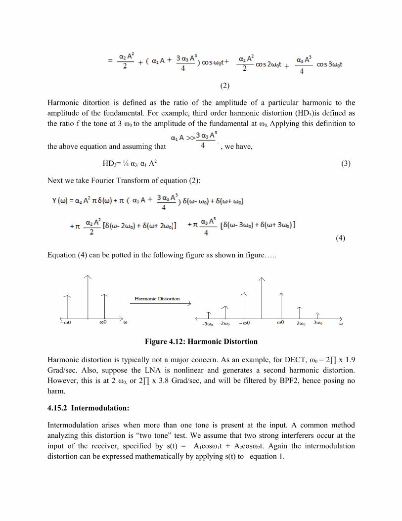
(2)
Harmonic ditortion is defined as the ratio of the amplitude of a particular harmonic to the amplitude of the fundamental. For example, third order harmonic distortion (HD3)is defined as the ratio f the tone at 3 ω0 to the amplitude of the fundamental at ω0. Applying this definition to
the above equation and assuming that , we have,
HD3= ¼ α3/ α1 A2 (3)
Next we take Fourier Transform of equation (2):
(4)
Equation (4) can be potted in the following figure as shown in figure…..
Figure 4.12: Harmonic Distortion
Harmonic distortion is typically not a major concern. As an example, for DECT, ω0 = 2∏ x 1.9 Grad/sec. Also, suppose the LNA is nonlinear and generates a second harmonic distortion. However, this is at 2 ω0, or 2∏ x 3.8 Grad/sec, and will be filtered by BPF2, hence posing no harm.
4.15.2 Intermodulation:
Intermodulation arises when more than one tone is present at the input. A common method analyzing this distortion is “two tone” test. We assume that two strong interferers occur at the input of the receiver, specified by s(t) = A1cosω1t + A2cosω2t. Again the intermodulation distortion can be expressed mathematically by applying s(t) to equation 1.

y(t)= α1 (A1cosω1t + A2cosω2t) + α2(A1cosω1t + A2cosω2t)2 + α3 (A1cosω1t + A2cosω2t)3 (5)
using trigonometric manipulations, we can find expression for the second and the third order intermodulation product as follows:
ω1 ± ω2 : α2 A1A2 cos(ω1 + ω2) t + α2 A1A2 cos(ω1 - ω2) t;
2ω1 ± ω2 : 3α3 A12A2 /4 cos(2ω1 + ω2) t + 3α3 A1
2A2 /4 cos(2ω1 - ω2) t;
2ω2 ± ω1: 3α3 A22A1 /4 cos(2ω2 + ω1) t + 3α3 A2
2A1 /4 cos(2ω2 - ω1) t (6)
The output spectrum in the frequency domain can be determined from equation (6) by evaluating its Fourier transform Y(ω). This is shown in the following figure:
Figure 4.13: Intermodulation
Here the output will be good when the receiver has a filter of very narrow bandwidth. The same thing has been achieved in the receiver we used. It can be seen from above figure that the intermodulation product with frequency 2ω2 - ω1 (denoted as the third order intermodulation product. ID3) lies at ω0 and corrupts the desired signal at ω0. Furthermore, ω1, ω2 are close to ω0; therefore trying to filter them out requires the filter bandwidth that is very narrow and impractical. Keeping down 2ω2 - ω1 by keeping the non linearity small is the only solution.
Where do the two tones, at ω1 and ω2 come from? They can be any one of the interference that we know. Strictly speaking, the interferers are not tones, but are more like narrowband noise. For simplicity, for the time being, we represent the interferer at the band from ω1 – ωchannel/2 to ω1 + ωchannel/2 as a single tone centered at ω1, with the rms value of the narrowband noise set equal to the amplitude of the tone, or A1. Similar representation is applied to the desired signal at the band from ω0 – ωchannel/2 to ω0 + ωchannel/2 and the interferer at the band from ω2 – ωchannel/2 to ω2 + ωchannel/2. To quantify this distortion, IM3, as the ratio of the amplitude of the ID3
to the amplitude of the fundamental output component (denoted as ID1) of a linear system given by y(t) = α1 A1 cosω0t, where α1 is the linear small signal gain. Mathematically, this is given as;
IM3 = ID3 / ID1. (7)

Note that IM3 expressed in decibels is simply the difference between the desired signal strength in decibels (at ω0) and the interferer strength in decibels (at 2ω2,1 - ω1,2). In order to quantify IM3, let us simplify by assuming A = A1 = A2. Applying equation (4) to (6) we get,
(8)
Comparing equation (3) to (8), it is seen that
IM3 = 3 HD3 (9)
Since IM3 depends on the input level and is sometimes not as easy to use, we define another performance metric, called the third order intercept point (IP3).
4.15.3 Third Order Intercept Point (IP3):
From equation (5) we note that as the input level A increases, the desired signal at the output is proportional to A (by the small gain α1). On the other hand from equation (6) we can see that the third order product ID3 increases in proportion to A3. This is plotted on a linear scale in following figure (a). Figure (a) is re-plotted on logarithmic scale in figure (b), where power level is used instead of amplitude level. As shown in figure (b), the power of ID3 grows at three times the rate at which the desired signal ID1 increases. The third order intercept point is defined IP3 is defined to be the intersection of the two lines.
Figure 4.14: Third Order Intercept Point (IP3)
Thus in summary it can be said that specially because of the EA modulation the result is improved but also the excellent receiver design also plays an important role for better performance of the system.

Chapter 5
Different Techniques forDifferent Techniques for Transporting RF Signals overTransporting RF Signals over
OFCOFC

CHAPTER
5Techniques for Transporting RF Signals
over Optical Fibre
Introduction
There are several optical techniques for generating and transporting microwave signals over fibre. By considering the frequency of the RF signal fed into the RoF link at the head end in comparison with the signal generated at the RAU the RoF techniques may be classified into three categories – namely RF-over-fibre (RFoF), IF-over-Fibre (IFoF), or baseband-over-Fibre (BBoF). RFoF involves the transmission of the actual RF signal over the fibre. However, in IFoF and BBoF the desired microwave signal is generated at the RAU through up-conversion with a LO, which is either provided separately at the RAU, or is transported remotely to the RAU. Therefore, depending on the transmission method used, the RAU may be more complex or simpler.
Schemes requiring a separate LO at the RAU (i.e. either BBoF or IFoF) may render the RAU more costly, especially in mm-wave applications. However, such systems e x h i b i t i m p r o v e d receiver sensitivity. A c o m p a r i s o n of the receiver sensitivities of three different RoF data transmission techniques – namely BBoF, IFoF, and RFoF is reported in. Using an IF signal frequency of 2 GHz, and a LO signal frequency at 27 GHz, the three schemes were used to generate a 29 GHz RF signal modulated with 155 Mbps downstream data.
It was found that the BBoF scheme exhibited better sensitivity than the IFoF scheme by 4 dB. On the other hand, the IFoF scheme had 2 dBs better sensitivity than the RFoF scheme.
The transport of wireless signals as RFoF has the advantage that simpler RAUs may be used, since no frequency up-conversion is required. But this comes at a co s t i n terms of the requirement for high-frequency equipment at the head-end. The RFoF system is also susceptible to the effects of fibre dispersion on the RF power and phase noise. A further disadvantage of RFoF is that it is susceptible to chromatic dispersion, which induces frequency- or length-dependent amplitude suppression of the RF power, if Double Side Band modulation of the optical signal is used. The amplitude suppression effect may be modelled by the modulation

transfer of the externally-modulated IM-DD system. BBoF and IFoF schemes may overcome such effects, but this may occur at the cost of increased RAU complexity, unless the upstream LO is delivered remotely.
RoF techniques may also be classified in terms of the underlying modulation/detection principles employed. In that case, the techniques may be grouped into three categories, namely Intensity Modulation – Direct Detection (IM- DD), Remote Heterodyne Detection (RHD), and harmonic up-conversion techniques. RFoF systems fall under the IM-DD category. IFoF and BBoF systems, which involve the use of a LO at the RAU may also employ IM-DD to transmit the baseband data or IF to the RAU. However, in most cases, IFoF and BBoF schemes rely on RHD for RF signal generation.
This chapter briefly covers basic optical fiber transmission link and surveys state-of-the-art RoF technologies with an emphasis on RoF system operating at mm-wave bands. This chapter mainly deals with two things as such: (1) RF signal generation and transportation techniques, and link configurations, (2) the state of the art on mm-wave generation and transport technologies. In addition, RoF with wavelength division multiplexing (WDM) is described as it has been one of the hot topics in this area. This chapter presents the principles behind the various RF signal transport methods and discusses their pros and cons. Where necessary, some examples of RoF systems are given to emphasize some aspects of the techniques involved.
5.1 A two stage modulation:
There are two entirely different forms of modulation/demodulation process involved in the RoF scheme. This can be better understood by looking at the fig 5.1.
Figure 5.1: A Closure Look at the Fiber Wireless Downlink

1. Modulating the RF carrier with the baseband information source at the central base station and corresponding demodulation at the portable unit. 2. Modulating the optical carrier with the RF signal at the laser and the corresponding demodulation at the optical receiver.To avoid confusion the first modulation will be referred to as baseband RF modulation and the second modulation will be referred to as RF optical modulation in this thesis.
5.2 Basic Radio Signal Generation and Transportation Methods:
In this section, a brief overview of how to generate and transport radio signal over an optical fiber in RoF networks is given. Virtually all of the optical links transmitting microwave/mm-wave signals apply intensity modulation of light. Essentially, three different methods exist for the transmission of microwave/mm-wave signals over optical links with intensity modulation: (1) direct intensity modulation, (2) external modulation, and (3) remote heterodyning. In direct intensity modulation an electrical parameter of the light source is modulated by the information-bearing RF signal. In practical links, this is the current of the laser diode serving as the optical transmitter. The second method applies an unmodulated light source and an external light intensity modulator. This technique is called “external modulation”. In a third method, RF signals are optically generated via remote heterodyning, that is, a method in which more than one optical signal is generated by the light source, one of which is modulated by the information-bearing signal and these are mixed or heterodyned by the photo detector or by an external mixer to form the output RF signal. The external modulation and heterodyne methods are discussed in more detail in subsequent subsections. In this subsection, we consider only direct intensity modulation.
Direct intensity modulation is the simplest of the three solutions. So it is used everywhere that it can be used. When it is combined with direct detection using PD, it is frequently referred to as intensity-modulation direct-detection (IMDD) (Fig. 5.2). A direct-modulation link is so named because a semiconductor laser directly converts a small-signal modulation (around a bias point set by a dc current) into a corresponding small-signal modulation of the intensity of photons emitted (around the average intensity at the bias point). Thus, a single device serves as the optical source and the RF/optical modulator. One limiting phenomenon to its use is the modulation bandwidth of the laser. Relatively simple lasers can be modulated upto frequencies of several gigahertz, say, 5–10 GHz. Although there are reports of direct intensity modulation lasers operating at up to 40 GHz or even higher, these diodes are rather expensive or nonexistent in commercial form. That is why at higher frequencies, say, above 10 GHz, external modulation rather than direct modulation is applied. In entering into the millimeter band a new adverse effect, such as the non convenient transfer function of the transmission medium, is observed. It

turns out that the fiber dispersion and coherent mixing of the sidebands of modulated light may cause transmission zeros, even in the case of rather moderate lengths of fiber. For example, a standard fiber having a one km length has a transmission zero at 60 GHz if 1.55 m wave-length light is intensity modulated. Due to this phenomenon, optical generation rather than transmission of the RF signal is preferable.
5.3 External & direct modulation:
The RF optical modulation is done either by directly modulating the optical source itself direct modulation) or by modulating the optical carrier after generation (external modulation). There are benefits and drawbacks in each of these approaches.
Direct modulation:
With this approach, the driving current of the optical source is directly modulated by the radio frequency signal. This method is robust, cost effective & gives adequate performance when the radio frequency is few GHz. The maximum bandwidth of the direct modulated link is about 20 GHz. However a directly modulated link severely attenuates the RF signal. The loss is about 39 db (without the fiber loss) for a resistively matched ROF link and 20 db for a relatively matched RoF link. Furthermore, directly modulated laser exhibits chirp and relative intensity noise, which are discussed later in this thesis. In this work, our focus is limited to the EA modulation.
Figure 5.2: The RF Optical Direct Modulation Scheme
External Modulation:
Figure 5.3: The RF Optical External Modulation Scheme

5.4 Mach-Zehnder Interferometer (MZI):
The most widely used external modulator is the Mach- Zehnder Interferometer. These modulators provide very high bandwidth and are capable of handling at least 400mW of continuous optical power and the gain of the externally modulated link is proportional to the square of the optical power. So very high gain links are achievable with bandwidth. However the non linearity starts to appear at high power levels. The MZI are expensive and require precise configuration.
5.5 Electro –absorption Modulator (EAM):
This is another type of the external modulator that is emerging in this field. Due to its multi quantum well structure, the EAM can also be optimized to detect the optical signals. This is very attractive for full duplex mode operation. These EAM are highly desirable to be used as single unit RAPs because, these are small, robust and more importantly enables a passive operation. Therefore they can be used as both O/E & E/O converters even without an external power supply.
5.6 RoF Link Configurations:
In this section we discuss a typical RoF link configuration, which is classified based on the kinds of frequency bands (baseband (BB), IF, RF bands) transmitted over an optical fiber link. Representative RoF link configurations are schematically shown in Fig. 5.4. Here, we assume that a BS has its own light source for explanation purpose; however, BS can be configured without light source for uplink transmission. Not only RF but also IF or baseband signal can be used to modulate LD, which is discussed earlier. In each configuration of the figure, BSs do not have any equipment for modulation and demodulation, only the CS has such equipment. In the downlink from the CS to the BSs, the information signal from a public switched telephone network (PSTN), the Internet, or other CS is fed into the modem in the CS. The signal that is either RF, IF or BB bands modulates optical signal from LD. As described earlier, if the RF band is low, we can modulate the LD signal by the signal of the RF band directly. If the RF band is high, such as the mm-wave band, we sometimes need to use external optical modulators (EOMs), like electro-absorption ones. The modulated optical signal is transmitted to the BSs via optical fiber. At the BSs, the RF/IF/BB band signal is recovered from the modulated optical signal by using a PD. The recovered signal, which needs to be up converted to RF band if IF or BB signal is transmitted, is transmitted to the MHs via the antennas of the BSs.

Figure 5.4: Intensity-Modulation Direct Detection (IM-DD) Analog Optical Link
In the configuration shown in Fig. 5.5 (a), the modulated signal is generated at the CS in an RF band and directly transmitted to the BSs by an EOM, which is called “RF-over-Fiber”. At each BS, the modulated signal is recovered by detecting the modulated optical signal with a PD and directly transmitted to the MHs. Signal distribution as RF-over-Fiber has the advantage of a simplified BS design but is susceptible to fiber chromatic dispersion that severely limits the transmission distance. In the configuration shown in Fig. 5.5 (b), the modulated signal is generated at the CS in an IF band and transmitted to the BSs by an EOM, which is called “IF-over-Fiber”. At each BS, the modulated signal is recovered by detecting the modulated optical signal with a PD, up converted to an RF band, and transmitted to the MHs. In this scheme, the effect of fiber chromatic dispersion on the distribution of IF signals is much reduced, although antenna BSs implemented for RoF system incorporating IF-over-Fiber transport require additional electronic hardware such as a mm-wave frequency LO for frequency up- and down conversion. In the configuration (c) of the figure, the modulated signal is generated at the CS in baseband and transmitted to the BSs by an EOM, which is referred to as “`BB-over-Fiber”. At each BS, the modulated signal is recovered by detecting the modulated optical signal with a PD, up converted to an RF band through an IF band or directly, and transmitted to the MHs. In the baseband transmission, influence of the fiber dispersion effect is negligible, but the BS configuration is the most complex. Since, without a subcarrier frequency, it has no choice but to adopt time-division or code-division multiplexing. In the configuration shown in Fig. 5.5 (d), the modulated signal is generated at the CS in a baseband or an IF band and transmitted to the BSs by modulating a LD directly. At each BS, the modulated signal is recovered by detecting the modulated optical signal with a PD, up converted to an RF band, and transmitted to the MHs. This is feasible for relatively low frequencies, say, less than 10 GHz.
By reducing the frequency band used to generate the modulated signal at the CS such as IF-over-Fiber or BB-over-Fiber, the bandwidth required for optical modulation can greatly be reduced. This is especially important when RoF at mm-wave bands is combined with dense wavelength division multiplexing (DWDM). However, this increases the amount of equipment at the BSs because an up converter for the downlink and a down converter for the uplink are required. In the RF subcarrier transmission, the BS configuration can be simplified only if mm-wave optical external modulator and a high-frequency PD are respectively applied to the

electric-to-optic (E/O) and the optic-to-electric (O/E) converters.
For the uplink from an MH to the CS, the reverse process is performed. In the configuration shown in Fig. 5.5 (a), the signals received at a BS are amplified and directly transmitted to the CS by modulating an optical signal from a LD by using an EOM. In the configuration (b) and (c), the signals received at a BS are amplified and down converted to an IF or a baseband frequency and transmitted to the CS by modulating an optical signal from a LD by using an EOM. In the configuration (d), the signals received at a BS are amplified and down-converted to an IF or a baseband frequency and transmitted to the CS by directly modulating an optical signal from a LD.
Figure 5.5: Representative RoF Link Configurations. (a)EOM, RF modulated signal; (b) EOM, IF modulated signal; (c) EOM, baseband modulated signal; (d) Direct Modulation
5.7 State-of-the-Art Millimeter-wave Generation and Transport Technologies:
Recently, a lot of research has been carried out to develop mm-wave generation and transport techniques, which include the optical generation of low phase noise wireless signals and their transport overcoming the chromatic dispersion in fiber. Several state-of-the-art techniques that have been investigated so far are described in this section, which are classified into the following four categories:

1. optical heterodyning2. external modulation 3. up- and down-conversion 4. optical transceiver
5.8 Optical Heterodyning:
Many RoF techniques rely on the principle of Remote Heterodyne Detection (RHD), where two optical carriers are coherently mixed in the photodiode. Several methods may be used to generate the optical carriers, including, optical FM/PM, sideband generation with the Mach Zehnder intensity Modulator, and dual mode lasers. With RHD, RF signals at very high frequencies (limited only by photo-detector bandwidth) may b e g e n e r a t e d . However, the requirement for additional beat frequency stabilization and phase noise suppression schemes in RHD-based RoF systems, renders them rather complex. These schemes include optical phase/frequency locked loops, and optical injection locking, or a combination of both.
In optical heterodyning technique, two or more optical signals are simultaneously transmitted and are heterodyned in the receiver. One or more of the heterodyning products is the required RF signal. For example, two optical signals with a wavelength separation of 0.5 nm at 1550 nm will generate a beat frequency of around 60 GHz. Heterodyning can be realized by the PD itself or the optical signals can be detected separately and then converted in an electrical (RF) mixer. In a complete (duplex) system, the PD can be replaced by an electro-absorption transceiver.
Figure 5.6: Optical Heterodyning
Because phase noise is a key problem in digital microwave/mm-wave transmission, care must be taken to produce a small phase noise only by the heterodyned signals. This can be achieved if the two (or more) optical signals are phase coherent; in turn, this can be realized if the different frequency optical signals are somehow deduced from a common source or they are

phase-locked to one master source. Benefits of this approach are that (1) it overcomes chromatic dispersion effect and (2) it offers flexibility in frequency since frequencies from some megahertz up to the terahertz-region is possible. However, it uses either a precisely biased electro optic modulator or sophisticated lasers.
Fig. 5.6 shows a typical design of optical heterodyning. The master laser's intensity is modulated by the unmodulated RF reference signal; several harmonics of the reference signal and consequently several sidebands are generated. The reference laser is injection locked by one of these and the signal laser by another one in such a way that the difference of their frequencies corresponds to the mm-wave local oscillator frequency. And, as seen, the optical field generated by the signal laser is also modulated by the information-bearing IF signal.
5.9 External modulation:
Although direct intensity modulation is by far the simplest, due to the limited modulation bandwidth of the laser this is not suitable for mm-wave bands. This is the reason why at higher frequencies, say, above 10 GHz, external modulation rather than direct modulation is applied. External modulation is done by a high speed external modulator such as electro-absorption modulator (EAM). Its configuration is simple, but it has some disadvantages such as fiber dispersion effect and high insertion loss. Representative configurations are shown in Fig. 5.5 (a)–(c), where intensity modulation is employed.
In conventional intensity modulation, the optical carrier is modulated to generate an optical field with the carrier and double sidebands (DSB). When the signal is sent over fiber, chromatic dispersion causes each spectral component to experience different phase shifts depending on the fiber link distance, modulation frequency, and the fiber dispersion parameter. If the relative phase between these two components is 180º, the components destructively interfere and the mm-wave electrical signal disappears. To reduce such dispersion effects, optical single-sideband (SSB) is widely used. Specially designed EAM was developed and experimented at 60 GHz band RoF system in while a Mach-Zehnder modulator (MZM) and a fiber Bragg grating filter were used in to produce single-sideband optical modulation.
5.10 Up- and Down-conversion:
In this technique IF band signal is transported over optical fiber instead of RF band signal. The transport of the IF-band optical signal is almost free from the fiber dispersion effect; however, the electrical frequency conversion between the IF-band and mm-wave requires frequency mixers and a mm-wave LO, resulting in the additional cost to the BS. Another advantage of this technique is the fact that it occupies small amount of bandwidth, which is especially beneficial when the system is combined with DWDM as is described in section 3.3.5. A representative

configuration is shown in Fig. 3.8 (b).
5.11 Optical Transceiver:
The simplest BS structure can be implemented with an optical transceiver such as electro-absorption transceiver (EAT). It serves both as an O/E converter for the downlink and an E/O converter for the uplink at the same time. Two wavelengths are transmitted over an optical fiber from the CS to BS. One of them for downlink transmission is modulated by user data while the other for uplink transmission is unmodulated. The unmodulated wavelength is modulated by uplink data at the BS and returns to the CS. That is, an EAT is used as the photodiode for the data path and also as a modulator to provide a return path for the data, thereby removing the need for a laser at the remote site. This device has been shown to be capable of full duplex operation in several experiments at mm-wave bands. A drawback is that it suffers from chromatic dispersion problem. Fig. 5.7 shows RoF system based on EAT. Note that two frequencies are required here.
Figure 5.7: Electro-absorption Transceiver (EAT)
Summary:
In this chapter a brief description of conventional optical transmission link and basic optical components was given, and RoF technologies have been described including typical RoF link configurations, state-of-the-art mm-wave generation and transport techniques. Due to its potentiality to support broadband service with little infrastructure and many advantages such as cost-effectiveness, easy deployment, maintenance RoF networks will be a promising alternative to future wireless networks. Thus in this chapter we have reviewed state-of-the art techniques for

distributing RF signals over fibre optic links. The different RoF techniques for transporting RF signals over optical fibers may be classified in terms of the frequency at which the signals are transported or the underlying optical modulation/detection principles involved. In terms of frequency, RoF techniques may be classified as RF-over-fibre, IF-over fibre, or baseband-over-fibre. In terms of modulation/detection, they may be classified as Intensity Modulation – with Direct Detection (IM-DD), Remote Heterodyne Detection (RHD), or harmonic up-conversion. Therefore a RoF technique may belong to one or more categories, or may combine the different aspects of several techniques.

Chapter 6
The Experimental Set-UpThe Experimental Set-Up

1
CHAPTER
6
The Experimental Set-Up
The experimental set-up for the study of radio over fiber link was based on the following motivations and objectives:
1. Generation and detection of 3G cellular signals2. Characterization of LASER diode and study of non linearity introduced by directly
modulated laser diode3. Study of different methods used earlier to remove non linearity observed in direct
modulation of the laser diode4. Estimate the extent of non linearity in case of external modulation of the laser5. Find the suitability of the externally modulated laser diode ROF link for long haul
communication6. Study noise characteristics of ROF Link
6.1 The radio over Fiber link:
The radio over fiber link was introduced and its various characteristics have been outlined in earlier chapters. In this chapter, an in-depth discussion of an externally modulated RoF link is presented. This is done by both theoretical analysis and by empirical measurements. At the end of this chapter it will be clear that some link parameters are critically important for transmitting radio signals for wireless access; while, others turn out to be less significant.
The RoF set consists of three main elements: an optical source (laser) with an RF-modulating arrangement, a single mode fiber link and an optical receiver with a band-pass filter to recover the original signal. In addition an RF amplifier is included at the optical receiver. Each of these elements is reviewed in detail in this chapter.
The set up of radio over fiber technique is given in Figure 6.1. In figure 6.1, the first block is WCDMA signal generator. In fact we can use any signal generator as RF source; but in this research work we are proposing the use of the radio over fiber technology for the 3G cellular system; accordingly WCDMA signal generator has been selected.

Fig 6.1: Basic ROF technique set-up
In our experimental work, we have used TSW3003 as a WCDMA generator. The carrier frequency of the WCDMA is 2.14 GHz. Thus this block acts as source of analog modulating signal. Earlier we have seen that there occur two stage modulations in the radio over fiber technology. The first stage of the modulation, i.e. modulating the radio frequency sub-carrier is performed in this block. Then the second block is laser diode module. In our experimental work we have used Bookham’s EML100Z laser diode modulator. This is a 10 Gbps Electro-absorption modulator. The analog modulating signal from the first block modulates the laser diode in this block. The modulation type employed here is intensity modulation. This device acts as E/O converter. Then the third and last block is optical receiver. In our experimental work we have used PIN diode receiver from Discovery Semiconductors named as Lab Buddy. This Lab Buddy is in fact an O/E converter.
6.2 Experimental Set-up to implement ROF technique:
Given fig 6.2 shows the experimental set-up used for radio signal transmission over fiber optic link. GC101 is the main card while GC5316 is a daughter card. PC communicates with the GC5316 daughter card via GC 101 main card. The use of the main card and daughter card assembly is to convert the text file in the PC into I/Q vector. The procedure of getting I/Q vector is as such: PC puts it’s text file into the input module of GC101 main card. Then GC101 supplies these text file to GC5316. Then GC5316 converts this text file to I/Q vector. After the conversion the GC5316 stores these I/Q vector into the output module of GC 101. Then PC gets the access to these I/Q vector and then it supplies these I/Q vectors to the TSW3003 as a modulating signal which performs QPSK modulation of the radio frequency carrier. This modulated signal is nothing but the WCDMA signal. Hence output of TSW3003 is radio frequency. Thus we can say that TSW3003 is responsible for the digital to analog conversion. This radio signal passes through coaxial cable and is then fed to 1350nm laser diode modulator. There happens electro absorption effect inside the laser diode modulator. This laser beam modulated by the radio frequency signal is passed through the fiber optic cable.

Fig 6.2: Experimental set-up for implementation of ROF link
Then at the receiving end, pin diode and low noise amplifier converts optical signal to the electrical form. This 2.14GHz electrical signal at the receiver is down converted to 2.14MHz. TSW2100 applies clock signal to GC101. AFC8406 is a wide band amplifier, which converts 24.4MHz signal to I/Q vector, which is then applied, to PC-III.
By using the experimental set up shown above, we have measured the WCDMA signal quality. For this measurement a signal generator and a signal analyzer are used. The different parameters which we have measured include first harmonic frequency, modulation depth, bandwidth of the carrier, complementary cumulative distributive function (CCDF), Amplitude Probability Distribution (APD), total harmonic distortion (THD), carrier to noise ratio, occupied bandwidth, received power, sweep time etc . Determination of the first harmonic frequency is a very crucial thing because we know that it plays very important role in system performance and non linearity.
6.3 IMPLEMENTATION DETAILS OF EXPERIMENT:
The experiments performed by us were concentrated basically on WCDMA standard. Steps to perform the same are explained below.

1. Start GC Studio2. Click on File > New Project 3. Choose a name for the new project, and click create4. Select GC5316 for the Plug-in and click OK5. Using the wizard style interface, setup the GC101 evaluation board, and then click next
"Evaluation Board Setup" Menu allows the user to set up the data source (input and output), pattern length, capture length, and clock rates and sources. At this point, click the "NEXT" tab to proceed to the next screen
6. Setup the GC5316 I/O mode selection. In this the ADC clock rate is set depending on the signals used i.e. 1 for WCDMA and ¾ for CDMA
7. Set the simulated clock rate to 122.88 MHz and click next8. Channel Copying is to be skipped , click Next9. Project description can be added to explain the details. Finish the set-up Wizard by
clicking the “Finish” tab on the next screen10. Click on the large GC5316 box to display the global control registers11. Next, double click on the GC5316 block to “push down” one level into the GC531612. Click on the Input Interface block to display and edit receive input interface registers. Set
adc_fifo_bypass to FALSE to enable the rxin_a/b/c/d input FIFO circuits.13. Click on the upper Receive Channel 0 blocks. Set ddc_duc_ena to True. Make sure that
the cdma_mode is set to False for WCDMA signal14. Click on the area circled by "Load from File" that Loads the stimulus
file“TM1_300k_IF19.2_Fup122.88_1000.GCIN” provided on CD. This file will simulate a real TM1 WCDMA signal at an IF of 19.2 MHz
15. Click on the Receive Input Interface section, and then make sure that the "resampler_decimate" is set to "FALSE"
16. Next, click on Receive Channel 0, and make sure cdma_mode is set to "False". Set the NCO Frequency (freqa) to 19.2 (MHz). Re-set the "ch_rate_sel" to 0 to guarantee this register gets set properly
17. Double-click on Receive Channel 0 to define the parameters inside the channel. Click on the "Delay Adjust and Zero Pad" box. Since the ADC will run at the DDC rate, “tadj_interp_dec” bit needs to be set to 0, to interpolate by 1
18. The CIC filter decimates by 8, and the CIC shifter gain needs to be scaled19. The CFIR is 32 taps long with the coefficients loaded from the
file"UMTS_CFIR_32.taps", which is located on the provided CD20. The PFIR is 64 taps long, decimating by 1. Load coefficients from the file
“UMTS_PFIR_64.taps21. Set the gain of PFIR to "1"22. Click on the "AGC" block and set the registers23. Select the Serial Interface block and set the parameters as indicated. Set the number of
output bits to 16 (“pser_recv_bits” = 15). No clock division is used. After verifying the

values of the serial interface, click the arrow as shown in Figure below to pop up one level in the GC5316hierarchy
Figure 6.3: GC Studio Setting
24. Receive Channel 0 has now been configured to process:
• Four WCDMA signals at 122.88 MSPS
• Mixer/NCOs block shifts the signal to DC
• The CIC block decimates by 8x to 15.36 MSPS
• 32-tap CFIR compensates for the CIC droop, filters and decimates the signal to 7.68 MSPS
• 64-tap PFIR filters the signal
• Channel AGC is set
• Serial interface is used to output the base band signal at serial output clock of 122.88 MHz
25. Copy the Receive Channel 0 settings to Receive Channel 7 by going to Parameter ® GC5316Channel Copy
26. Next, click on the icon circled as shown in Figure below for the graphical display settings:
Figure 6.4: GC Studio Setting
27. Click the Add New Data Source button circled shown in Figure below

Figure 6.5: GC Studio Setting
28. In the Choose Source panel, select Receive Output Port A 0, and click OK29. In the graph panel, set the Plot Type to Spectral Magnitude, and check Logarithmic30. Again, click on the plot button to open another plot to view the input data31. Click the Add New Data Source button circled as shown in Figure below
Figure 6.6: GC Studio Setting
32. In the Choose Source panel, select Receive Input Port 0, and click OK33. On the GC Studio panel, click the Build and Load buttons, circled in Figure below. This
will execute the experiment
Figure 6.7: GC Studio Setting

34. The graph window will be automatically updated with the results 35. On the GC Studio panel, click on the stop button, shown circled below, to stop the
experiment, and then select File ® Save Project to save this project36. Close the GC Studio Graph Window
6.3.1 WCDMA Steps:1. Four real WCDMA carriers is applied to the GC5316 rxin_a2. Simulated rx_clk to the GC5316 is 122.88MHz3. Receive FIFOs are enabled4. Receive Channels 0-3 are configured to process the signal5. Channel NCOs tune to four different IF frequencies6. The CIC filter is programmed to decimate by 5. The output sample rate at the CIC output
is 15.36Msps7. The CFIR filter compensates for the drop in the CIC filter, and provides some low pass
filtering. It is configured as a 20 tap filter.8. The 40 tap PFIR provides final symbol shaping and filtering9. Channel AGC is configured as fixed unity gain10. Baseband data is transmitted and captured using the serial interface at the full rx_clk rate.
TECHNICAL DETAILS OF EXPERIMENT:
6.4. GC5316:
6.4.1 GC5316 Power and Ground Signal Description:
VDUT1 – 3.3V power from GC101 EVM to the daughter card, GND 3.3V power for the GC5316 daughter card can be supplied by the GC101 motherboard or
an external power supply. A regulator on the daughter card can be used to generate the 1.5V core supply voltage or an external supply can be used.
Jumper W1 – Selects source for GC5316 core 1.5V power position 1:2 selects an external supply connected to J2 for the 1.5V core supply position 2:3 selects the regulator on the daughter card as the 1.5V core supply Jumper W2 Selects source for GC5316 I/O 3.3V power position 1:2 selects an external supply connected to J3 for the 3.3V I/O supply position 2:3 selects the GC101 motherboard as the source for the 3.3V I/O supply
The GC5316 core power supply is 1.5V. The daughter card includes a regulator that can be used to supply this 1.5V to the GC5316 or an external power supply can be connected at J2.
The GC5316 I/O power supply is 3.3V, and can be supplied by the GC101 motherboard or an external power supply connected to J3.
6.4.2 GC 5316 Specifications:

The GC5316 is a high-density multi-channel communications signal processor integrated circuit that provides both digital down conversion and digital up conversion optimized for cellular base transceiver systems.
The device supports both UMTS and CDMA2000 (CDMA) air interface cellular standards.
The chip provides up to 24 CDMA digital down converter (DDC) and digital up converter (DUC) channels or 12 UMTSDDC and DUC channels.
The GC5316 can also support a combination of CDMA and UMTS channels. The DDC and DUC channels are independent and operate simultaneously.
The chip is ideal for cellular base transceiver systems where a large number of digital radio channels are required.
Each of the 24 CDMA (or 12 UMTS) channels can operate independently. On the DDC side there are four 16 bit input ports that can accept real or complex input
data. The input ports driven it parallel data, typically from an analog-to-digital converter. Each down converter channel can be programmed to accept data from any one of the four input ports.
On the DUC side, there are four 18-bit output ports. Each output port can sum any of the DUC channels in a daisy-chain fashion. This permits creating a stack of CDMA or UMTS signals.
These ports can output either real or complex data. Real output data would generally drive one or more D/A converters and output the stack of signals at an intermediate frequency (IF).
Complex data (at base band or an IF) is used when a quadrature modulator up conversion scheme is employed. Complex output data can also be used when the output stack is further processed using crest factor reduction or power amplifier pre distortion techniques.
The GC5316 transmit section provides up to 24 CDMA2000 or 12 UMTS digital up conversion (DUC) channels. There are 12 DUC blocks, DUC 0 through DUC 11. Each block can be configured as a single UMTS channel or two CDMA channels.
The outputs of all DUCs drive four independent complex sum chains. Any DUC can contribute (or not) to any or all the four sum chains. The output of a DUC
block’s sum chain drives the sum chain input of the next block. The first DUC to output data is DUC 0, while the last is DUC11. The four outputs of a DUC are the sum of all the contributing channels of all the higher numbered DUC blocks and it. The sum chain inputs of DUC 11 are grounded.
Within the chain, all DUC blocks from 0 up to the highest numbered DUC in use must be turned on otherwise the sum chain is broken.
The transmit output interface takes the four summed chains of DUC output data from the output of DUC 0 and then scales and rounds to a user-programmed number of bits.

Figure 6.8: GC5316 Transmit Section
Composite power meters with programmable integration periods and intervals compute the power in each of the four output streams.
The data is then formatted for output over the four tx_data_out outputs.
6.4.3 Key Features of GC 5316:
Optimized for CDMA2000®-1X and UMTS systems1) Up to 12 UMTS or 24 CDMA2000 down converter and up converter channels2) Mixed CDMA2000-1X and UMTS operation
3) DDC input and DUC output rates to 125 MSPS
4) Any DDC can connect to any of four input ports

5) Any DUC can sum into any of four output ports6) Real/complex DDC inputs and DUC outputs
7) Programmable AGC on DDC outputs8) Rx filtering: 6-stage CIC, 48-tap CFIR, 64-tap PFIR9) Tx filtering: 6-stage CIC, 47-tap CFIR, 63-tap PFIR10) 115 dB SFDR11) 16-bit DDC inputs, 18-bit DUC outputs
6.5 GC studio:
Because the GC series of Texas Instruments parts are complex devices and must be programmed using a microprocessor interface; an Evaluation Module (EVM) has been developed to demonstrate and test their capabilities. The GC Studio program controls the evaluation board and provides an intuitive user interface for programming the GC parts.
A DSP device can be thought of as a Multiple Input, Multiple Output Transfer Function (MIMO Transfer Function). It expects a stream of stimulus data and then produces a stream of response data.
The primary use of the GC101 EVM is to program the Device under Test (DUT), provide a stream of stimulus information, and capture the response information for processing by the computer.
The GC Studio software controls the GC101 EVM and provides a stimulus image as well as retrieving and processing the response image.
The DUC block accepts base band serial data. At this point the gain can be adjusted and a pilot sequence can be summed with the data. Power can be measured, and then the data is pulse-shape filtered and interpolated to a higher rate.
6.6 GC101:
The GC101 EVM is a motherboard style platform designed to evaluate individual Texas Instruments-Gray chip devices installed on daughter boards.
The platform interfaces to the daughter boards through a 168 pin Dual Inline Memory Module (DIMM) style connector.
The EVM interfaces to a host computer over an ECP IEEE1284 interface. The EVM provides internal DC power based on an external 5V input.
The EVM provides digital stimulus and digital monitoring of the daughter card. Multiple devices can be evaluated using a common EVM platform with different
daughter boards and PC software. External digital input and output interfaces are provided on the GC101 EVM.
External clock and synchronization signals are also provided. The on-board memory allows the user to download test patterns and capture processed data with a PC using the provided software.

The two digital input connectors allow the user to provide test patterns via an external source.
A logic analyzer or digital-to-analog converter EVM can be used to monitor processed data through the output connectors. The host computer interface controls the EVM operation from a PC.
The software supplied allows the user to write or read from the control and page registers of the daughter card under test.
Fig below shows an interface diagram of the components that make up a typical GC evaluation system
Figure 6.9: Interface Diagram for GC Evaluation System
6.6.1 GC101 Details:
The EVM provides the DC power, local bus programming, clock, data path, digital stimulus, digital monitoring, and local PC host control interface to test a GC101 daughter card.
The DC power is provided from a set of regulators that convert the 5v external power to local EVM power of 1.8vdc and 3.3vdc.

Additional power supplies are provided for daughter card 2.5v and 3.3vdc.Additional external power supplies are provided for additional (2) dedicated power supplies on the daughter card.
The Local Bus programming is provided through the local PC host control interface. The clock and data path control provide for internal clock generation, internal sync generation, internal data stimulus, or external signals.
The digital monitoring can be provided in all modes, and can be stored in memory and/or output to the digital interface.
The EVM provides a 36 bit stimulus and monitoring path for the daughter card. The 36bit path consists of a memory or external input data, input sync, and input clock. The EVM has an internal 10 MHz oscillator to develop a 40, 60, 80, 100, or 120 MHz internal clock. The EVM has an internal PLL that provides for clock multiplication of 1,2,4,6,8,10, and 12.
The digital clock can select the Analog PLL or reference clock signal. The clock oscillator is in a socket, and can be changed to a different clock rate. A clock can be provided internally from the digital input connector, or from a SMA external input.
There are two 40pin digital input and output headers for the external input and output data. The sync signal can also be supplied internally, through the external data input, or through an SMA connector.
PC software is supplied to control the EVM. The PC software uses a custom script language to program the EVM.
The PC software is available in either a batch processing (Text User Interface) or with a Graphic Control interface (Graphic User Interface). The PC software is installed with the Graphics User software for each daughter card.
6.7 GC5316 Daughter card and GC101 EVM Setup:
The GC5316 is a high density digital up converter and down converter. It is optimized for UMTS, TD-SCDMA and CDMA2000-1X standards.
It provides 12 UMTS up conversion and 12 UMTS down conversion channels. Alternately, the chip can handle 24 CDMA up conversion and down conversion channels.
The GC5316 daughter card for the GC101Motherboard provides a means for testing and evaluating this part, using the GC Studio program for device control.
To operate the system, simply plug the GC5316 daughter card into the DIMM socket on the GC101 motherboard, connect the parallel port interface cable to the GC101 and Host Computer (PC), and connect the power supply to the GC101.

Figure 6.10: GC101 EVM and GC5316 Daughter card

1
CHAPTER
7
Observations
7.1 Which observations were recorded?
The main experimental work in the current research is the verification of different waveforms and characteristics of the radio frequency signal as obtained from the electro-absorption modulation. With this thing in mind, we performed the experiment first to analyze the unmodulated pure WCDMA signal obtained from TSW3003 on the spectrum analyzer. To obtain the pure carrier, we set the modulating signal bit pattern adjustment as provided in internal ADC of TSW3003 equal to zero. Thus a pure unmodulated WCDMA signal (here referred to as carrier from communication point of view) is obtained. Theoretically the frequency of this radio frequency signal is 2.14GHz. For the verification purpose, this signal was applied to the spectrum analyzer. Then the waveform we got is as shown in figure 7.1. From this figure we see that we obtained excellent output, i.e. there is no frequency deviation from the center frequency, at least of visible range. Thus here we can comment that the performance of the WCDMA generator is upto the mark. Further we also measured the harmonic content of the carrier signal, but no appreciable harmonics were recorded. Then the same spectrum called as radio frequency sub-carrier is applied to the laser diode module. In our case, the laser diode module uses electro-absorption type of the external modulation. This laser diode modulator acts as an E/O converter. The operating wavelength of the laser diode is 1450nm. Then the optical output from the laser diode is coupled into the optical fiber cable. Thus two wavelengths are travelling through the fiber; one is optical carrier, and the second is radio frequency sub-carrier (of 2.14GHz frequency). Then the second end of the optical fiber cable (called as patch cord) is connected to optical detector (i.e. PIN diode detector named as Lab Buddy by Discovery Semiconductors). This detector operates as O/E converter; i.e. output of the detector is radio frequency signal. Then this RF signal is applied to the spectrum analyzer to view the detected waveform. The waveform we got is given in figure 7.2. On the spectrum analyzer, we saw excellent waveforms; i.e. from our earlier discussion, we know that in case of the direct modulation, different non

linearties arise, and to overcome those non linearties a combination of different methods have to be applied. But in the present case since we have used electro-absorption modulation there is no requirement of non linearity compensation techniques as already we got a fairly linear signal.
Then the next thing to be done was to find out the extent of the carrier signal impairment as it passes through the optical fiber cable. In fact when the optical signal passes through the OFC, it mainly encounters attenuation and dispersion. These two phenomena mainly limit the distance between two repeaters, in our case the distance between the central base station and radio access point. We could see the effect of attenuation on the received signal by using Noyce’s made attenuator and we observed that there is no significant signal impairment at least upto 40km length of the optical fiber link. The waveform obtained by providing the variable attenuation to the carrier is also observed on the spectrum analyzer.
Then the next step was to modulate the carrier either by using internal ADC settings or by I/Q vector. We performed such modulation of the WCDMA carrier and observed the modulated output of the TSW3003 on the spectrum analyzer. This waveform is as shown in figure 7.3. Again all the procedures which were applied to the pure carrier are repeated for the modulated signal also; i.e. first the signal is applied to the laser diode modulator, then the optical output from the LDM is coupled to OFC and then the second end of the OFC is connected to the lab buddy. Then the output of the lab buddy is applied to the spectrum analyzer and we got the waveform as shown in figure 7.5. Again the modulated signal is attenuated and applied to the spectrum analyzer, and we got fairly good results. This result indicates that our assembly can be used to build-up a fiber feeder network required in radio over fiber technology for interconnection of head-end and remote RAUs.
Then the amplitude probability distribution function of the modulated carrier signal is measured on the spectrum analyzer and it is as shown in figure 7.6. For 100000 samples, the mean amplitude was found to be -52.43dBm, the peak amplitude was found to be -50.82dBm, and the crest amplitude was found to be 1.83dB. Then we measured complementary cumulative distributive function of the carrier on the spectrum analyzer and it is as shown in figure 7.7. For 100000 numbers of samples, mean was found to be -52.36dBm, peak was found to be -50.71dBm, and the crest was found to be 1.65dB. Then we measured total harmonic distortion of the modulated carrier on the spectrum analyzer, and it is as shown in figure 7.8. Then on the spectrum analyzer we measured other important parameters of the modulated carrier with respect to the parameters of the WCDMA signal and that is as shown in figure 7.9. The different parameters which we recorded here include the transmission channel bandwidth equal to 3.84MHz, transmission channel power equal to -51.73dBm, adjacent channel bandwidth equal to 3.84MHz and so on as given in figure itself. Thus we can observe that both the unmodulated carrier and modulated carrier preserved its features after being transmitted through the optical fiber cable. Thus it is evident that the radio over fiber technology can be used for sparsely populated rural areas to interconnect the RAUs and can also be used for road vehicular

communication system (RVC). Also this technology is useful in in-building wireless signal penetration by forming the pico-cells and micro-cells.
Figure 7.1: Pure Carrier signal obtained directly from TSW3003 WCDMA Generator

Figure 7.2: Pure Carrier signal obtained from Lab Buddy
Figure 7.3: WCDMA Modulated Signal obtained from TSW3003

Figure 7.4: WCDMA Modulated Signal obtained from Lab Buddy
Figure 7.5: WCDMA modulated signal obtained after passing it to fiber length of few kms

Figure 7.6: Amplitude PDF of the WCDMA signal
Figure 7.7: Complementary CDF of the WCDMA signal

Figure 7.8: Total Harmonic Distortion of the WCDMA signal
Figure 7.9: Carrier Signal w.r.t. WCDMA standard

7.2 The first basic Measurement recorded: First in this experiment we applied the WCDMA carrier signal i.e. output from the TSW 3003 to the spectrum analyzer. This waveform is analyzed properly, various parameters from this waveform were recorded and the waveform itself was saved on the spectrum analyzer. Second, in the experiment process pure WCDMA carrier from TSW3003 was applied to laser diode module. Then the output of the laser diode module was transmitted through the optical fiber cable of approximately 12km length. Then the light wave from the other end of the optical fiber cable was applied to lab buddy which acts as detector. Then we applied the output of the lab buddy to the spectrum analyzer. In this case also the various parameters of the wave were recorded on the spectrum analyzer and also this waveform itself was saved on the spectrum analyzer. Then the reading from the first case and the second case were analyzed and we got the surprisingly good result; i.e. both the waveforms were exactly identical, at least to the extent as much as we could perceive. We concluded that this exceptionally good result is due to the electro-absorption modulation. The connection diagrams for both the cases are shown in the following figure.
Fig 7.10: Connection diagram for analyzing WCDMA signal directly on Spectrum analyzer
Fig 7.11: Connection diagram for analyzing WCDMA signal after passing through the optical fiber
The actual waveform observed in above connection is as depicted in the above plates. In the figure 7.12 we can observe the expected theoretical waveform for a one tone test, i.e. a single optical frequency is injected into the optical fiber. When compared these figure with the actual waveforms that we obtained in our research work (shown in plates), we can comment that both are fairly alike. Thus we can comment here that our experimental results are consistent with the theoretical result. Thus we can say that the electro-absorption modulation based ROF link can be used for fiber feeder network as required in this technology to connect CS and RAUs.

Figure 7.12: A single Tone at the input and output of ROF link
7.3 Dynamic Range & Amplitude and Phase Response: We have seen earlier that dynamic range of the link is a very important factor which influences the link’s performance. This dynamic range depends upon the noise floor. The noise floor of the ROF link using direct modulation has been found as given in the following figure. From figure 7.13 it is observed that carrier power and noise power have a linear relationship in case there is no optical fiber whereas there is non linear relationship between the two when the optical fiber is interconnected. Thus with optical link noise power is inherently more. But in case of the external EAM the noise power decreases significantly. Figure 7.14 gives the amplitude in dBm as a function of the frequency passing through the optical fiber.

Figure 7.13: Noise Floor Measurement at the ROF Link
Figure 7.14: Frequency Dependent Noise Floor of the ROF link
Similarly the amplitude and phase response of the RoF link with two different input powers was recorded as shown in the following figure 7.15. From this figure we observe that the gain of the ROF link is a function of the optical input power. Thus we can calculate the optimum power to be launched into the optical fiber so as to have the maximum efficiency. From below figure we observe that the gain of the fiber is higher for a power level of -20dBm than 5dBm. Similarly we observe that the phase response of the ROF link is also a function of the power in optical fiber.

Figure 7.15: Amplitude Response of the ROF Link with two Different Input Powers
Figure 7.16: Phase Response of the ROF Link with two Different Input Powers
There are different methods to counteract with this non linearity produced by the optical fiber and laser. One of these methods is simulation method. Here we mathematically model the complete RoF link and then use the inverse function of the non linearity model. In that particularly following methods are used.
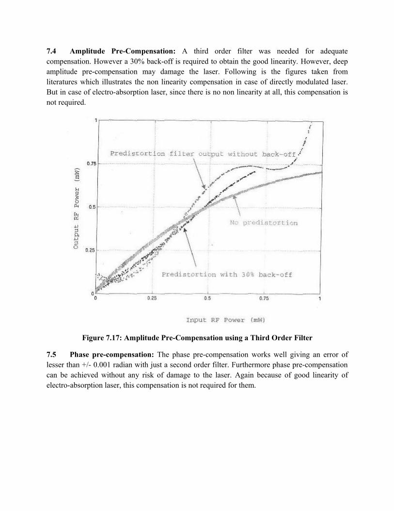
7.4 Amplitude Pre-Compensation: A third order filter was needed for adequate compensation. However a 30% back-off is required to obtain the good linearity. However, deep amplitude pre-compensation may damage the laser. Following is the figures taken from literatures which illustrates the non linearity compensation in case of directly modulated laser. But in case of electro-absorption laser, since there is no non linearity at all, this compensation is not required.
Figure 7.17: Amplitude Pre-Compensation using a Third Order Filter
7.5 Phase pre-compensation: The phase pre-compensation works well giving an error of lesser than +/- 0.001 radian with just a second order filter. Furthermore phase pre-compensation can be achieved without any risk of damage to the laser. Again because of good linearity of electro-absorption laser, this compensation is not required for them.

Chapter 8
Results and DiscussionResults and Discussion
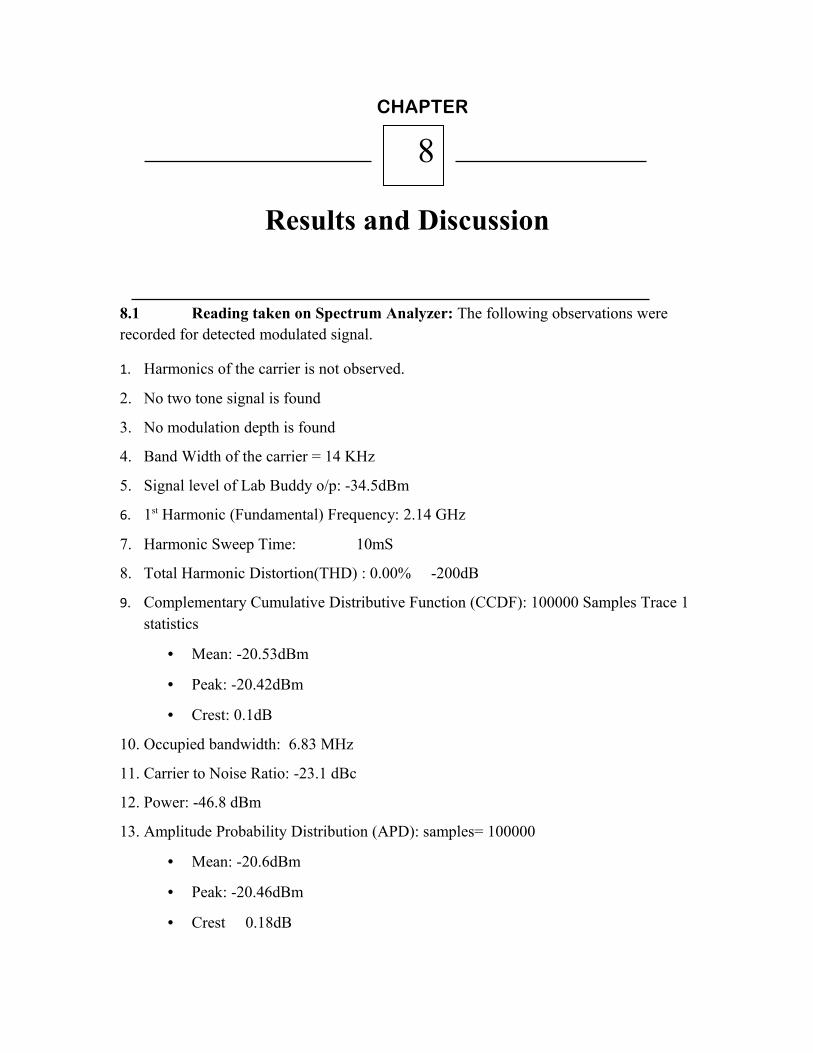
1
CHAPTER
8
Results and Discussion
8.1 Reading taken on Spectrum Analyzer: The following observations were recorded for detected modulated signal.
1. Harmonics of the carrier is not observed.
2. No two tone signal is found
3. No modulation depth is found
4. Band Width of the carrier = 14 KHz
5. Signal level of Lab Buddy o/p: -34.5dBm
6. 1st Harmonic (Fundamental) Frequency: 2.14 GHz
7. Harmonic Sweep Time: 10mS
8. Total Harmonic Distortion(THD) : 0.00% -200dB
9. Complementary Cumulative Distributive Function (CCDF): 100000 Samples Trace 1 statistics
• Mean: -20.53dBm
• Peak: -20.42dBm
• Crest: 0.1dB
10. Occupied bandwidth: 6.83 MHz
11. Carrier to Noise Ratio: -23.1 dBc
12. Power: -46.8 dBm
13. Amplitude Probability Distribution (APD): samples= 100000
• Mean: -20.6dBm
• Peak: -20.46dBm
• Crest 0.18dB

8.2 Reading at different wavelength of light: We know that the attenuation characteristic of the fiber is directly dependent upon the wavelength of the light passing through the fiber. The optical output from the laser diode module is applied to optical power meter and the following observation has been made.
Sr. No
Wavelength Power received
1 780nm -0.70dBm2 850nm 5.15dBm3 1300nm 0.40dBm4 1310nm 0.35dBm5 1550nm 6.55dBm
Finally the various advantages, limitations and application of this technology can be enlisted as mentioned below:
8.3 Benefits of RoF Technology
1. Low Attenuation Loss:
In t r a n s m i s s i o n l i n e s , impedance rises with frequency as well, leading to very high losses at microwave frequencies. Therefore, distributing high frequency radio signals electrically over long distances requires expensive regenerating equipment. As for mm-waves, their distribution via the use of transmission lines is not feasible even for short distances. The alternative solution to this problem is to distribute baseband signals or signals at low intermediate frequencies (IF) from the switching centre (head-end) to the BS. The baseband or IF signals are up-converted to the required microwave or mm-wave frequency at each base station, amplified and then radiated. This system configuration is the same as the one used in the distribution of narrowband mobile communication systems shown in Figure 1.3. Since, high performance LOs would be required for up-conversion at each base station, this arrangement leads to complex base stations with tight performance requirements. However, since optical fibre offers very low loss, RoF technology can be used to achieve both low-loss distribution of mm-waves, and simplification of RAUs at the same time.
Commercially available standard Single Mode Fibers (SMFs) made from glass (silica) have attenuation losses below 0.2dB/km and 0.5dB/km in the 1550 nm and the 1300 nm windows, respectively. These losses are much lower than those encountered in; say coaxial cable, whose losses are higher by three orders of magnitude at higher frequencies. For instance, the attenuation of a ½ inch coaxial cable (RG-214) is >500 dB/km for frequencies above 5 GHz. Therefore, by transmitting microwaves in the optical form, transmission distances are increased several folds and the required transmission powers reduced greatly.

2. Large Bandwidth:
Optical f i b e r o f f e r e n o r m o u s b a n d w i d t h . There a r e t h r e e m a i n t r a n s m i s s i o n windows, which offer low attenuation, namely the 850 nm, 1310 nm, and 1550 nm wavelengths. For a single SMF optical fibre, the combined bandwidth of the three windows i s in the exces s o f 50 THz . However, today’s state-of-the-art commercial systems utilize only a fraction of this capacity (1.6 THz). But developments to exploit more optical capacity per single fibre are still continuing. The main driving force towards unlocking more and more bandwidth out of the optical fibre include the availability of low dispersion fibre, the Erbium Doped Fibre Amplifier (EDFA) for the 1550 nm window, and the use of advanced multiplex techniques namely Optical Time Division Multiplexing (OTDM) in combination with Dense Wavelength Division Multiplex (DWDM) techniques.
3. High Speed Signal Processing in the optical domain:
The high optical bandwidth enables high speed signal processing that may be more difficult or impossible to do in electronic systems. In other words, some of the demanding microwave functions such as filtering, mixing, up- and down-conversion, can be implemented in the optical domain. For instance, mm-wave filtering can be achieved by first converting the electrical signal to be filtered into an optical signal, then performing the filtering by using optical components such as the Mach Zehnder Interferometer (MZI) or Fibre Bragg Gratings (FBG), and then converting the filtered signal back into electrical form. Furthermore, processing in the optical domain makes it possible to use cheaper low bandwidth optical components such as laser diodes and modulators, and still be able to handle high bandwidth signals.
4. Multiplexing Optical Channel to Overcome Electronic Bottleneck:
The utilization of the enormous bandwidth offered by optical fibers is severely hampered by the limitation in bandwidth of electronic systems, which are the primary sources and receivers of transmission data. This problem is referred to as the “electronic bottleneck”. The solution around the electronic bottleneck lies in effective multiplexing. OTDM and DWDM techniques mentioned above are used in digital optical systems. In analog optical systems including RoF technology, Sub-Carrier Multiplexing (SCM) is used to increase optical fibre bandwidth utilization. In SCM, several microwave subcarriers, which are modulated with digital or analog data, are combined and used to modulate the optical signal, which is then carried on a single fibre. This makes RoF systems cost-effective.
5. Immunity to Radio Frequency Interference:
Because of this immunity, fibre cables are preferred for microwave transmission and even for short connections at mm-waves. EMI immunity is the immunity to eavesdropping, which

is an important characteristic of optical fibre communications, as it provides privacy and security.
6. Easy Installation and Maintenance:
Easy installation and low maintenance costs of RAUs are very important requirements for mm-wave systems, because of the large numbers of the required RAUs. In applications where RAUs are not easily accessible, the reduction in maintenance requirements leads to major operational cost savings. Smaller RAUs also lead to reduced environmental impact.
7. Low Cost Technique Because of Simplified BS:
In RoF systems, complex and expensive equipment is kept at the head-end, thereby making the RAUs simpler. For instance, most RoF techniques eliminate the need for a LO and related equipment at the RAU. In such cases a photo detector, an RF amplifier, and an antenna make up the RAU. Modulation and switching equipment is kept in the head-end and is shared by several RAUs. This arrangement leads to smaller and lighter RAUs, effectively reducing system installation and maintenance costs.
8. Reduced Power Consumption:
Reduced power consumption is a consequence of having simple RAUs with reduced equipment. In some applications, the RAUs are operated in passive mode. Reduced power consumption at the RAU is significant considering that RAUs are sometimes placed in remote locations not fed by the power grid.
9. Multi-Operator and Multi-Service Operation:
RoF offers system operational flexibility. Depending on the microwave generation technique, the RoF distribution system can be made signal-format transparent.
10. Dynamic Resource Allocation:
Since the switching, modulation, and other RF functions are performed at a centralized head-end, it is possible to allocate capacity dynamically.
11. Future Proof:
Fiber Optics are designed to handle gigabits speeds which means they will be able to handle speeds offered by future generations of networks for years to come. RoF technology is also protocol and bit-rate transparent, hence, can be employed to use any current and future technologies.

Above advantages are for radio over fiber technology in general. But since ROF link is not much flexible using direct modulation, we can say that all above advantages can be exploited to the maximum extent only when we are using electro-absorption modulation. Apart from these advantages of radio over fiber there are few advantages of exclusively electro-absorption modulation (that we used in our research work) and these are listed as below:
1. Zero biasing voltage2. Low Driving voltage3. Low/ Negative chirp4. Ultra-low energy consumption for modulation in the optics domain5. >10 dB Extinction ratio6. Very small footprint (30 µm2)7. Operation spectrum width covering half of the C-band for on-chip WDM8. Overcomes intrinsic non linearity of the laser9. Lesser Polarization dependence10. Integration with DFB laser11. Allows a single optical power source to be used for large number of information
carrying beams
8.4 Limitation of Direct Modulation type and it’s solution using EAM:
The response of directly modulated laser is highly non linear. This is a major drawbacks of the directly modulated laser used in ROF technology and thus the use of this technology is limited only to short haul communication. But using the electro-absorption modulation used in our research work, the laser response can be made highly linear and thus the ROF technology is worth to be used for long haul communication. These results can be observed from the plates attached in observation chapter.
8.5 Limitations of RoF Technology
Since RoF involves analog modulation, and detection of light, it is fundamentally an analog transmission system. Therefore, signal impairments such as noise and distortion, which are important in analog communication systems, are important in RoF systems as well. These impairments tend to limit the Noise Figure (NF) and Dynamic Range (DR) of the RoF links. DR is a very important parameter for mobile (cellular) communication systems such as GSM because the power received at the BS from the MUs varies widely (e.g. 80dB). That is, the RF power received from a MU which is close to the BS can be much higher than the RF power received from a MU which is several kilo-meters away, but within the same cell.
The noise sources in analog optical fibre links include the laser’s Relative Intensity Noise
(RIN), the laser’s phase noise, the photodiode’s shot noise, the amplifier’s thermal noise, and the fiber’s dispersion. In Single Mode Fibre (SMF) based RoF systems, chromatic dispersion may limit the fibre link lengths and may also cause phase de-correlation leading to increased RF carrier phase noise. In Multi-Mode Fibre based RoF systems, modal dispersion severely limits the available link bandwidth and distance. It must be stated that although the RoF transmission system itself is analog, the radio system being distributed need not be analog as well, but it may be digital (e.g. WLAN, UMTS), using comprehensive multi-level signal modulation formats such as x-QAM, or Orthogonal Frequency Division Multiplexing (OFDM).
Last mile: Although fiber-optic systems excel in high-bandwidth applications, optical fiber has been slow to achieve its goal of fiber to the premises or to solve the last mile problem. However, as bandwidth demand increases, more and more progress towards this goal can be observed. In Japan, for instance, fiber-optic systems are beginning to replace wire-based DSL as a broadband Internet source. The same applies to the Scandinavian countries. South Korea’s KT also provides a service called FTTH (Fiber to the Home), which provides 100 percent fiber-optic connections to the subscriber’s home. Verizon, a US based telecom company, provides a service called FiOS which offers TV, high-speed internet, and telephone communications on a 100 percent fiber-optic network to a junction box mounted in a subscriber’s home.
8.5.1 Major limitations:
The RoF link has enough bandwidth to support many wideband wireless channels. When the radio frequency is only a few GHz, and the fiber length is only a few kilometers, fiber dispersion and laser chirp is not a concern. However when the wireless link is in series with the optical link, the non linear distortion in the ROF link is the biggest concern. Laser diode’s intrinsic non linearity is considered as the major source of this NLD in a directly modulated link. However in our research project, we have used external modulation of the laser thus there is no more the problem with laser’s intrinsic non linearity. This is severe in the uplink because of multipath fading of the wireless channel. Even in the downlink a good dynamic range is required because the number of active users keep varying. For example in IS-95, the number of downlink channels can vary from 9 to 64.
The dynamic range requirement is more severe than we would imagine. In a typical micro cellular environment, the distance from a portable unit to the radio access point can vary from few meters to about 300 meters. In addition the average path loss of the wireless link can vary from d-1.5 to d-4 depending upon the obstacles in between. Thus in indoor pico-cell the radio signals can fluctuate by 40-55dB and in outdoor microcells this fluctuation can be as high as 80-90dB. This amount can vary by 10dB with varying environmental characteristics. The dynamic range has to be added with the minimum acceptable carrier to interference ratio of the particular

modulation scheme. For example, a C/I ratio of 16dB is required for IS-54. In addition, the linear range of given device inherently goes down with an increasing bandwidth. This is aggravated by the fact that the noise power increases with the signal band width, which, in tern, decreases the DR. Hence, the wider the signal bandwidth, the more severe is the non linear distortion. This postulates a severe constraints’ on the linearity requirement to support wide band multimedia eservices. For example, the DR requirement is much severe for wide band CDMA type systems than narrowband systems.
From the literature, we found that the DR available from a typical RoF link is 20-30dB less than what is needed to serves a typical micro cell. Because the number of BSs is high in RoF networks, simple and cost-effective components must be utilized. Therefore, in the uplink of a RoF network system, it is convenient to use direct intensity modulation with cheap lasers; this may require down conversion of the uplink RF signal received at the BS. In the downlink either lasers or external modulators can be used.
8.6 Applications of RoF Technology
(a) RoF technology is generally unsuitable for system applications, where high Spurious Free Dynamic Range (SFDR = maximum output signal power for which the power of the third-order inter modulation product is equal to the noise floor) is required, because of the limited DR. This is especially true of wide coverage mobile systems such as GSM, where SFDR of > 70 dB (outdoor) are required. However, most indoor applications do not require high SFDR. For instance, the required (uplink) SFDR for GSM reduces from >70 dB to about 50 dB for indoor applications. Therefore, RoF distribution systems can readily be used for in-building (indoor) distribution of wireless signals of both mobile and data communication (e.g. WLAN) systems. In this case the RoF system becomes a Distributed Antenna System (DAS). For high- frequency applications such as WPAN, the cell size will be small due to high losses through the walls, bringing the benefits of RoF discussed above. The in-building fibre infrastructure may then be used for both wired and wireless applications. Using MMF or indeed POF instead of SMF fibres to feed the RAUs may further reduce system installation and maintenance costs, especially for in-door applications. In-building data communication LANs are often based on MMF.
(b) RoF systems are also attractive for other present and future applications where high SFDR is not required. For instance, UMTS MUs are required to control their transmitter power so that equal power levels are received at the BS. Thus, UMTS does not need the high SFDR required in GSM, so that RoF distribution systems may be used for both indoor and outdoor UMTS signal distribution . Another application area is in Fixed Wireless Access (FWA) systems, such as WiMAX, where RoF technology may be used to optically transport signals over long distances bringing the significantly simplified RAUs closer to the end user, from

where wireless links help to achieve broadband first/last mile access, in a cost effective way.
(c) Radio Coverage Extension:- ROF extends the reach of an existing base station to one or more location that are
shadowed or obstructed in terms of propagation of radio waves.- Several cellular service providers have deployed ROF as the standard solution for
highway and railway tunnels in European countries (Germany, Austria, and Italy) to complement and enhance the solutions based on RF repeaters. The RF repeaters amplifies both forward and reverse path signals to appropriate level in order to drive the ROF systems
(d) Capacity distribution and allocation:- It includes application for subway stations, exhibition grounds, airports, downtown
street levels and other densely populated environments where the traffic requirement leads to dedicated radio channels that need to be distributed appropriately.
- Many remote units are connected to a dedicated base station via fiber cables and the systems normally have a star configuration and share the ROF system.
(e) Applications on World-wide basis:- Australia has widely used ROF for outdoor capacity applications. Telstra (incumbent
Australian landline and mobile operator) has used ROF systems since 1993 for their Advanced Mobile Phone System (AMPS) network and further migrations to GSM .They deployed a real outdoor street level micro cellular layer in Melbourne and Sydney with more than 300 remote units mounted on light poles in downtown areas.
- The mobile network operators of South Korea adopted ROF around the mid 1990’s to distribute the capacity of CDMA systems at 800 and 1800 MHz with medium and high power fiber remote units.
(f) Access to dead zones:An important application of RoF is its use to provide wireless coverage in the area where wireless backhaul link is not possible. These zones can be areas inside a structure such as a tunnel, areas behind buildings, Mountainous places or secluded areas such a jungle.
(g) FTTA (Fiber to the Antenna):By using an optical connection directly to the antenna, the equipment vendor can gain several advantages like low line losses, immunity to lightening strikes/electric discharges and reduced complexity of base station by attaching light weight Optical-to-Electrical (O/E) converter directly to antenna.

Chapter 9

1
CHAPTER
9
Conclusion & Future Scope
We have seen that for increasing the bandwidth of the system, more number of base stations needs to be deployed in the market. At present the cost of the base station is very high. Thus the cost of the base station is a major hurdle for implementing the concept of pico cells. This problem is solved using the concept of radio over fiber. In this technique the optical carrier is modulated by the radio frequency signal itself. Thus there is no need of analog to digital conversion of the modulating signal as done in the on/off keying type of modulation. Now this analog modulation can be accomplished in two ways: Earlier one called as direct modulation, and the current technique which we have used in this project is called as EA modulation. From the observation chapter, we see that by using the EA technique, we are getting excellent result as compared to the direct modulation. For example, the non linearity, harmonic distortion, third order intercept point, chromatic dispersion all are within the acceptable limits.
For quick understanding of the whole concept, let us consider the following case of uplink transmission. I want to send my voice “Hello” towards the other end. Then the first thing which will occur is my speech will be converted to digital form using CELP coding technique in the mobile handset. Then these digital codes modulate the radio frequency sub-carrier. In fact this radio frequency sub-carrier is supplied by central base station to base station and then by base station to the mobile host. This modulated radio frequency sub-carrier is received by the base station called as RAP. Then the base station performs the optical modulation of the laser (in our case electro absorption modulation). Thus the signal which goes from base station to central base station has two carriers, one is optical carrier and the other is radio frequency sub-carrier. Then the central base station uses an optical detector (PIN diode-LAB buddy in our case) to separate out radio frequency sub carrier from the received optical signal. Thus the central base station performs the O/E conversion process. Finally this signal is applied to the MSC of the cellular network. Now there will be occurrence of downlink transmission. Here the central base station receives the radio frequency signal from the MSC. Then there occurs E/O conversion at the CBS and the two radio frequency wavelengths embedded in optical frequency are sent from CBS to BS. On one wavelength there is modulated radio frequency carrier while on the other

wavelength there is pure carrier. The BS then performs O/E conversion and delievers the signal onto the second radio frequency signal provided by the CBS.
Increase of traffic and increase of operating frequency will most likely lead to 4G (fourth generation) mobile systems to much smaller cells than one applied presently. As a consequence, economic reasons will force architectures to be significantly different from existing ones. One such possible solution can be RoF, a technique in which wireless and optical techniques are jointly applied. In the conception of this technique accent was put on simplifying base stations by making RF (microwave/millimeter wave) design much simpler. In this paper it is shown that channel allocation, or more generally, radio resource management can also be made much simplified.
RoF links have microwave / millimeter wave transducers of rather advantageous characteristics, i.e. their insertion loss and their noise figure can be made rather low. Applying advanced optical techniques, design of base stations can be surprisingly simple particularly in the low-power case. It can also be noted that some of the optical impairments may result in poor RF properties; however, techniques counteracting these are available.
The proposed experimental set up for ROF implementation for 3G cellular system will help us in following respects:
• Generation & detection of 3G cellular signals• Characterization of laser diode and estimation of the non linearity introduced by directly
modulated laser diode
• Identification of the methods to remove the non linearity
• Study of noise characteristics of the RoF link
• Explore various application of this technologyMost RoF techniques utilize SMF to feed the RAUs, because the bandwidth of MMFs is severely limited by modal dispersion. However, most existing in-building fibre infrastructure for data communication is of a MMF nature. As a result many current RoF techniques may be used only for outdoor (SMF dominates) applications, but not indoor coverage (over MMFs).
The demand for broadband access has grown steadily as users experience the convenience of high-speed response combined with “always-on” connectivity. A broadband wireless access network (BWAN) is indeed a cost-effective alternative in providing users with such broadband services since it requires much less infrastructure compared to wire-line access networks such as x-DSL and cable modem networks. Thus, these days the so-called “wireless last mile” has attracted much attention. However, it has been concerned mainly with densely populated urban areas. Recent survey shows that although penetration of personal computers in rural areas is significant in some countries most of the users still use low-speed dial-up modem

for the Internet access. Since in such case broadband services based on wire-line networks are prohibitively expensive, wireless access network might be the best solution. It requires a large number of BSs to cover broad areas, while the traffic demand per BS is much lower compared to densely populate urban areas. Thus in this study, we propose RoF architecture for implementing low cost base stations.
The theoretical study for the feasibility of the remote delivery of pure high-frequency microwave signals to a significantly simplified Remote Antenna Unit (RAU) was done. However, considering the fact that real-time interactive multimedia services are increasingly becoming an important component of broadband wireless communication services, full-duplex communication is a must for the systems delivering these services. It is therefore imperative to extend the laboratory set-up to implement and demonstrate full-duplex RoF transmission with EAM. In addition to realize Full-Duplex Transmission, it is also interesting to investigate methods for achieving simple remote control of some of the RAU functions, when deemed necessary.
Most of the experimental work was conducted at frequencies around 2.14 GHz. In addition, electrical components required for implementing the RAU were easier to acquire. For the purpose of experimentally investigating and validating the performance of the EAM system, this frequency was found to be more than adequate. However, in terms of applicability, it is envisaged that the benefits of the EAM system will be greater at higher operating frequencies such as 60 GHz, due to availability of wide bandwidth, low signal phase noise, and long link lengths, while employing only low frequency electro-optical components at the headend and a simplified RAU. It is therefore, recommended that the EAM laboratory platform be upgraded to cover higher frequencies, including 60 GHz. This will make it possible to explore the use of the EAM system for some of the up-coming high density broadband wireless communication systems like IEEE 802.15 Wireless Personal Area Network (WPAN) standard (57 – 64 GHz), and the IEEE 802.16 Fixed Wireless Access standard (10 – 66 GHz). Clearly, these are application areas, where EAM or other RoF systems promise to be of great benefit.
Wireless coverage of the end-user domain, be it outdoors or indoors (in-building), is poised to become an essential part of broadband communication networks. In order to offer integrated broadband services (combining voice, data, video, multimedia services, and new value added services), these systems will need to offer higher data transmission capacities well beyond the present-day standards of wireless systems. Wireless LAN (IEEE802.11a/b/g) offering up-to 54 Mbps and operating at 2.4 GHz and 5 GHz, and 3G mobile networks (IMT2000/UMTS) offering up-to 2 Mbps and operating around 2 GHz, are some of today’s main wireless standards. IEEE802.16 or WiMAX is another recent standard aiming to bridge the last mile through mobile and fixed wireless access to the end user at frequencies between 2 – 66 GHz.

RoF is an analog optical link transmitting modulated RF signals. It serves to transmit the RF signals down- and uplink, i.e. To and from central stations (CS) to base stations (BS) called also radio ports. RF modulation is in most cases digital, in any usual form such as PSK, QAM, TCM, etc. Optical modulation might have in principle also various forms, however, intensity modulation (IM) is only dealt here as different schemes were virtually never proposed. The simplest method for transmitting RF signals over fibre is the RF over Fibre method using IM-DD, because no frequency up/down-conversion at the RAU is required. This leads to simple RAUs. However, high-frequency RoF system applications require complex high-frequency electro-optical interface equipment at the head-end, which leads to increased system costs, or poor performance. In addition, RFoF is susceptible to chromatic dispersion-induced carrier suppression when simple DSB modulation is used.
9.1 CHALLENGES:
Radio over fiber is a novel concept which helps to implement wideband / ultra wideband cellular communication system at a significant low cost. But there are few implementation challenges which are mentioned as below:
• Handling nonlinearity of laser diode and SM fiber
• Modeling concatenated channel and providing signal detection mechanism.
• Removing Chirp, which is an unwanted frequency modulation. When E/O conversion is done by directly modulating a laser diode, chirp distortion takes place. Effects of chirp involve input RF power, fiber dispersion & laser line width characteristics.
• Implementing suitable coding techniques to reduce the clipping distortion.
9.2 Future Possibilities and Extension in the research work
The proposed research work is mainly focused on studying the characteristics of WCDMA signal obtained from Electro-absorption type of laser instead of IM-DD type of laser. Thus it is proposed that WCDMA signal can be transmitted using radio over fiber technology. There are different possibilities for extension of the research work and they listed are as under:
1. In our research work, we have used double sideband modulation of the laser diode. But the chromatic dispersion effect is more severe in case of the double sideband modulation. Thus in order to improve the system the single sideband modulation of the laser diode can be done.
2. In present research work, the WCDMA signal has been modulated by using internal registers of ADC. Instead a pattern generator can be used to modulate WCDMA carrier and then this modulated WCDMA signal is transmitted and received. Here it is possible to find the bit error rate by using the assembly of attenuator and power meter.

3. It is possible to use the programmed EPROM chip instead of using the pattern generator. The data in the EPROM chip will modulate the WCDMA signal and then the modulated signal is applied to the receiver. The data in the EPROM chip may be sine wave, sinc wave or audio tone like hello and the same should be captured at the receiver side. The data to be fed to EPROM may be obtained from MATLAB or any other software tool. The clock rate for EPROM chip is equal to the system clock rate. Here also it is possible to find the BER by using the assembly of attenuator and power meter.
4. Presently we have used the scheme such that the single RF sub-carrier modulates the single optical wavelength. But in future by using the so called Sub-carrier multiplexing technique, a number of radio frequency sub-carrier can be used to modulate a single optical wavelength.
5. By using the technique of WDM, a number of optical wavelengths may be made to travel through the single optical fiber instead of one optical wavelength in one fiber case at present.
6. Centralized network architecture of RoF network suggests a new possibility for efficient resource management. In a wireless network based on cellular architecture resource management such as dynamic channel assignment, dynamic transmit power control, load balancing, mobility management and so on plays an important role. Resource management technique in such network requires access to information that must be gathered across a number of BSs and the technique involves controlled decision that applies a number of BSs, not just one. Thus some centralized decision making is appropriate. In this sense RoF networks have great potential for efficient resource management that might be hard to achieve in conventional distributed wireless architecture, implying so many open issues. But a lot of research work in this area is yet to be done.

Chapter 10
Summary of Publication

1
CHAPTER
10
The Summary of Publication
Paper presented in national conference at GGITM, Bhopal on 3G Mobile and Radio over Fiber scheduled on 20th & 21st November, 2009
Mr. S. R. Prasad, Prof. (Mrs) P. P. Kulkarni, and Prof. A. R. Nigwekar
KIT’s College of Engineering, Kolhapur
ABSTRACT - To meet the explosive demands of high capacity and broadband wireless access, modern cell based wireless networks have the trend to increase the number of cells by the process called as cell splitting and utilization of higher frequency bands. It leads to a large number of base stations to be deployed. In such cases ROF provides functionally simple base stations that are interconnected to a central control station via an optical fiber. This allows reduction in system cost. ROF is an analog optical link transmitting optical carrier modulated by the radio frequency signal. This technique facilitates to transmit radio frequency signal through the optical fiber in downlink and uplink.

Paper presented in inter national conference at Amrutvahini College of Engineering, Sangamner on 4G Mobile and Radio over Fiber on 4th & 5th March, 2009
Mr. S. R. Prasad, Prof. (Mrs) P. P. Kulkarni, and Prof. A. R. Nigwekar
KIT’s College of Engineering, Kolhapur
ABSTRACT - We know that for increasing the bandwidth of the system, more number of base stations needs to be deployed in the market. At present the cost of the base station is very high. Thus the cost of the base station is a major hurdle for implementing the concept of pico cells. This problem is solved using the concept of radio over fiber. In this technique the optical carrier is modulated by the radio frequency signal. Thus there is no need of analog to digital conversion of the modulating signal. Now this analog modulation can be accomplished in two ways: Earlier one called as direct modulation, and the current technique which we have used is called as EA modulation. We have observed in our experimental work that by using the EA technique, we are getting excellent result as compared to the direct modulation. For example, the non linearity, harmonic distortion, third order intercept point, chromatic dispersion, all are within the acceptable limits.

Chapter 11
References

1
CHAPTER
11
References
[1] S. Betti, A. Bizzotto, E. Brovi and M. Giaconi, “Effect of Semiconductor Laser Intrinsic Dynamic Distortion in Hybrid Fiber- CDMA Cellular Radio Network”, Microwave and Optical Technology Letters, Feb. 1999, Vol.20, No.3, pp. 207-211
[2] J. S. Wu, J. Wu, and H. W. Tsao, “A Radio over Fiber Network for Microcellular System Application”, IEEE transaction on Vehicular Technique, Vol.47, No.1, Feb. 1998
[3] K. Morita and H. Ohtsuka, “The New Generation of Wireless Communication Based on Fiber Radio Technologies”, IEICE transaction on Communication, Vol.E-76B, No.9, pp.1061-1068, Sept.1993
[4] R. Ohmotto, H. Ohtsuka, and H. Ichikawa, “Fiber Optic Microcell Radio System with a Spectrum Delivery scheme”, IEEE Journal on Communication, Vol.II, No.7, pp.1108-1117, Sept.1993
[5] Schuh, R. E., Alping A., and Sundberg, E.: “Penalty Free GSM-1800 and WCDMA Radio over Fiber Transmission using Multimode Fiber an 850 nm VCSEL ”, Electron, Lett, 2003,39, pp.512-514
[6] Wake, D., Johansson, D., and Moodie, D. G.:”Passive picocell:a new concept in wireless network infrastructure”, Electron. Lett,1997, 33, pp. 404-406
[7] Wake, D., and Moodie, D. G.:”Passive picocell:prospect for increasing the radio range”, Tech. dig. Of the Int. Topical meeting on Microwave Photonics 1997, pp. 269-271
[8] Peter Hartmann, Xin Qian, Adrian Wonfor, Richard v. Penty, Ian H. White, “1-20 GHz directly modulated radio over MMf link”, University of Cambridge, Department of Engineering Magaine, pp. 43-46
[9] Geoff Smithson, “Introduction to Digital modulation schemes”, Plextek Ltd Magazine, Great Chesterford, pp. 1-9

[10] Alan J. Weissberger,”Advanced Wireless architecture to facilitate Coverage of Services Part-II Radio over Fiber architecture”, WCA Meeting Proceding, Octber 17, 2006, pp. 1-4
[11] Andy Howard, “Direct-conversion I-Q modulation Simulation”, Agilent Technologies Magazine, pp. 1-21
[12] Noah Schmitz, Randy Becker, “Fading simulation made Easy”, Agilent Technologies Magazine, July 24, 2003, pp. 1-35
[13] Johan Kirkhorn, “Introduction to I-Q demodulation of RF-data”, IFBT, NTNU magazine, September 15, 1999 pp. 1-13
[14] C. Ziomek and P. Corredoura, “Digital I/Q Demodulator”, Standford Linear Accelerator Center, Standford magazine, pp. 56-58
[15] Istvan Frigys, “Radio over Fiber: Application, Basic Design and impact on Resourcenmanagement”
[16] Frederic Lucarz, Tabassam Ismail and Alwin Seeds, “Gigabit/s Wireless-over-Fiber systems, University College London Magazine, 2007, pp. 34-34-35
[17] M Garcia Larrode, A. M. J. Koonen and P. F. M. Smulders, “Imopact of Radio-over-Fiber links on the Wireless Access Protocols”, Cobra RESEARCH Institute magazine, Vol. 5, 2006, pp.56-56-59
[18] Abhay Joshi, Xinde Wang, Dan Mohr, Don Becker, and Christoph Wree, “Balanced Photo-receivers for analog and digital fiber optic communications”, SPIE Vol. 5814, pp. 39-50
[19] H. S. Al-Raweshidy, “Radio over Fiber for Next Generation Network”, School of Engineering and Design Magazine, Bruntel University
[20] K. A. Person, A. Alping, and D. Wake, “WCDMA Radio-over-Fiber transmission experiment using electro-absorption transceiver”, Electronics Letters, 23rd June 2005 Vol. 41 No. 13
[21] Vorgelet Von, “Radio over Fiber based Network Architecture”, A Ph. D. thesis submitted to University of Berlin
[22] Xavier N. Fernando, “Signal processing for Optical Fiber based Wireless Access”
[23] Anthony Ng’oma, “Radio over Fiber technology for Broadband Wireless Communication Systems”, A Ph. D. thesis submitted to Technische Universiteit
[24] Radio over Fiber Distribution System Note by Advanced Communications Research and Development, pp.1-5

[25] U. Gliese, T. N. Nielsen, S. Norskov, and K. E. Stubkjaer, “Multifunction Fibre-Optic Microwave Links Based on Remote Heterodyne Detection”, IEEE Trans. On Microwave Theory and Techniques, Vol. 46, No. 5, 458 - 468, (1998).
[26] P. Hartmann, M. Webster, A. Wonfor, J.D. Ingam, R.V. Penty, I.H. White, D.Wake, and A.J. Seeds, “Low-Cost Multimode Fiber-based Wireless LAN Distribution Systems Using Uncooled, Directly Modulated DFB Laser Diodes”, in Proceedings of the ECOC’03, Vol. 3, 2003, pp. 804 – 805.
[27] I. Frigyes, “Basic Microwave Properties of Optical Links: Insertion Loss, Noise Figure, and Modulation Transfer” in Radio over Fiber Technologies for Mobile Communications Networks”, H. Al-Raweshidy, and S. Komaki, ed. (Artech House, Inc, USA, 2002).
[28] J. Capmany, B. Ortega, A. Martinez, D. Pastor, M. Popov, and P. Y. Fonjallaz, “Multiwavelength Single Sideband Modulation for WDM Radio-Over-Fiber Systems Using a Fiber Grating Array Tandem Device”, IEEE Photonics Tech. Letters Vol. 17, No. 2, 471 - 473, (2005).
[29] Capmany, D. Pastor, P. Munoz, S. Sales, B. Ortega, and A. Martinez, “WDM-SSB Generation and Dispersion Mitigation in Radio over Fiber Systems with Improved Performance Using and AWG Multiplexer with Flat Top Resonances”, in Proceedings of the International Topical Meeting on Microwave Photonics (MWP 2003). 2003, pp. 39 – 42.
[30] J. Heiskala, and J. Terry, “OFDM Wireless LANs: A Theoretical and Practical Guide”, (Sams Publishing, USA, 2002), Chapt. 5.
[31] H. Al Raweshidi, S. Komaki (ed): Radio over Fiber …, Artech House, London, Boston, 2002
[32] I. Katzela and M. Naghshineh, “Channel assignment schemes for cellular mobile telecommunication systems: A compre-hensive survey,” IEEE Pers. Commun. Mag., vol.3, pp. 10–31, June 1996
[33] X. Qiu, K. Chawla, J. Chuang, and N. Sollenberger, “Network-Assisted Resource Management for Wireless Data Networks”, IEEE Journal on Selected Areas in Communications, vol. 19, no. 7, pp. 1222-1234, July 2001
[34] R. H. Frendiel, B. R. Badrinath, J. Borres, and R. D. Yates, “The infostations challenge: Balancing cost and ubiquity in delivering wirelessdata,” IEEE Pers. Commun. Mag., vol. 7, pp. 66–71, Apr. 2000.
[35] H. Furuta, M. Maeda, T. Nomoto, J. Kobayashi, and S. Kawasaki, “Optical Injection Locking of a 38-GHz-Band InP-Based HEMT Oscillator Using a 1.55-µm DSB-SC Modulated Lightwave”, IEEE Photonics Tech. Letters Vol. 11, NO 01, 19 - 21, (2001)

[36] C. G. Schaffer, F. H. Lubeck, R. P. Braun, G. Grosskopf, F. Schmidt, and M.Rohde, “Microwave Multichannel System with a Sideband Injection Locking Scheme in the 60 Ghz Band”, in Proceedings of the International Topical Meeting on Microwave Photonics (MWP 1998). 1998, pp. 67 - 69.
[37] S. Fukushima, C. F. C. Silva, Y. Muramoto, and A. J. Seeds, “10 to 110 GHz Tunable Opto-Electronic Frequency Synthesis Using Optical Frequency Comb Generator and Uni-Travelling-Carrier Photodiode”, IEEE Photonics Letters, Vol. 37, No. 12, 780 - 781, (2001).
[38] S. Bennett, B. Cai, E. Burr, O. Gough, and A. J. Seeds, “1.8 THz Bandwidth, Zero-Frequency Error, Tunable Optical Comb Generator for DWDM Applications”, IEEE Photonics Letters, Vol. 11, No. 5, 551 - 553, (1999).
[39] A. Johansson, and A. J. Seeds, “Millimeter-Wave Modulated Optical Signal Generation with High Spectral Purity and Wide-Locking Bandwidth Using a Fibre-Integrated Optical Injection Phase-Lock Loop”, IEEE Photonics Tech. Letters Vol. 12, NO. 6, 690 – 692, (2000)
[40] L. A. Johansson, and A. J. Seeds, “36 GHz 140-Mb/s Radio-Over-Fiber Transmission Unsing an Optical Injection Phase-Lock Loop Source”, IEEE Photonics Tech. Letters Vol. 13, NO 8, 893 - 895, (2001)
[41] R. H. Walden, “Analog-to-digital converter survey and analysis,” IEEE J. Select. Areas Commun, pp. 539–550, 1999
[42] J. C. Twitchell, P. W. Juodawlkis, J. L. Wasserman, R. C. Williamson, and G. E. Betts, “Extending the performance of optically sampled time-demultiplexed analog-to-digital converters,” in Conf. Lasers and Elec-trooptics Tech. Dig.. Washington, DC, 2000, Paper CFM2.
[43] T. R. Clark, J. U. Kang, and R. D. Esman, “Performance of a time-and wavelength-interleaved photonic sampler for analog–digital conver-sion,” IEEE Photon. Technol. Lett., vol. 11, pp. 1168–1170, 1999.
[44] F. Coppinger, A. S. Bhushan, and B. Jalali, “Photonic time stretch and its application to a44nalog-to-digital conversion”, IEEE Trans. Microwave Theory Tech., vol. 47, pp. 1309–1314, 1999
[45] P. Rabiei, and A. F. J. Levi, “Hybrid opto-electronic WDM ADC”, in Conf. Lasers and Electrooptics Tech. Dig, Washington, DC: Opt. Soc. Amer., 2000
[46] M. L. Dennis, W. K. Burns, T. F. Carruthers, and I. N. Duling, “Eight-to-one demultiplexing of 100-Gbit/s TDM data using LiNbO3 Sagnac interferometer modulators,” in Optical Fiber Communications Conf., vol. 2, 1998, pp. 110–112.

[47] Tektronix, “Digital Phosphor Oscilloscopes, Data Sheet,” Tektronix, Inc., Beaverton, OR, TDS7404, June 2000.
[48] M. L. Dennis, I. N. Duling, and W. K. Burns, “Inherently bias drift free amplitude modulator,” Electron. Lett., vol. 32, pp. 547–548, 1996.
[49] T. F. Carruthers and I. N. Duling III, “10-GHz, 1.3-ps erbium fiber laser employing soliton pulse shortening,” Opt. Lett., vol. 21, pp. 1927–1929, 1996.
[50] K. Iiyama, K. Hayashi, Y. Ida, H. Ikeda, and Y. Sakai, “Reflection-Type Delayed Self-Homodyne/Heterodyne Method for Optical Linewidth Measurements”, JLT, Vol. 9, No. 5, pp 635 - 640 (1991).
[51] A. Ng’oma,“Design of a Radio-over-Fiber System for Wireless LANs”, MTD.Report, Eindhoven University of Technology, Eindhoven, 2002.
[52] T. Koonen, A. Ng’oma, H. P. A. vd. Boom, I. Tafur Monroy, P. F. M. Smulders, and G. D. Khoe, “Microwave Signal Transport over Multimode Polymer Optical Fibre Networks for Feeding Wireless LAN Access Points”, in Proceedings of the European Conference on Optical Communications (ECOC’02). 2002, Paper 9.2.5.
[53] W. M. Hamdy, “Crosstalk in Direct Detection Optical FDMA Networks”, Ph.D. Thesis, Massachusetts Institute of Technology, Cambridge, 1991.
[54] A. Ng’oma, A. M. J. Koonen, I. Tafur-Monroy, H. P. A. vd. Boom, P. F. M.Smulders, and G. D. Khoe, “Optical Frequency Up-conversion in Multimode and Single-Mode Fibre Radio Systems”, in Proceedings of SPIE Vol. 5466,2004, pp 169 - 177.
[55] C. Cox and W. S. C. Chang, Chapter 1: Figures of merit and performance analysis of photonic microwave links, RF Photonic Technology in Optical Fiber Links, Edited by William S. C. Chang, 2002.
[56] A. M. Joshi and X. Wang, DC to 50 GHz Wide Bandwidth InGaAs Photodiodes and Photoreceivers, Proc. SPIE, CR73, p. 181, 1999.
[57] Hewlett-Packard Co, Fiber Optic Test and Measurement, Edited by Dennis Derickson, p. 272.
[58] A. M. Joshi, “Dynamic Range Analysis for the Photonic Time Delay Unit”, Discovery Semiconductors Inc. Technical Report to Georgia Tech., 2003.

[59] Wree, C., et al.: "Experimental Investigation of Receiver Sensitivity of RZ-DQPSK Modulation Format Using Balanced Detection", paper ThE5, Optical Fiber Communication Conference (OFC 2003), March 23-28, 2003, Atlanta, USA
[60] Wree, C., et al.: "High spectral efficiency 1.6b/s/Hz transmission (8x40Gb/s with a 25GHz grid) over 200km SSMF using RZ-DQPSK and polarization multiplexing", IEEE Photonics Technology Letters, September 2003, Vol. 15, No. 93, pp. 1303-1305
[61] J. Vobis, D. Derickson, “Optical Spectrum Analysis” in Fiber Optic Test and Measurement, D. Derickson, ed. (Prentice Hall Inc., New Jersey, 1998).
[62] A. Ng’oma T. Koonen, I. Tafur Monroy, H. P. A. vd. Boom, P. F. M. Smulders, and G. D. Khoe, “Distributing microwave signals via Polymer Optical Fiber (POF) System”, in Proceedings of the IEEE/LEOS Benelux Chapter Annual Symposium, 2001, pp 157 - 160.
Website References:
http://www.umtsworld.com
http://www.cdg.org
http://www.adc.com
http://www.lgcwireless.com
http://www.remec.com
http://foxcomwireless.com
http://www.tekmar.it
http://www.microwavephotonics.com
http://www.wikipedia.com
http://www.ti.com
http://www. agilent.com
http://www.bookham.com
http://www.amphenol.com
http://www. chipsat.com