r z scs-thomson 7# l 200 adjustable voltage and …
TRANSCRIPT
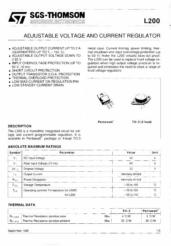
r z 7 S C S -T H O M S O N^ 7# L 200
ADJUSTABLE VOLTAGE AND CURRENT REGULATOR
. ADJUSTABLE OUTPUT CURRENT UP TO 2 A (GUARANTEED UP TO Tj = 150 °C)
. ADJUSTABLE OUTPUT VOLTAGE DOWN TO 2.85 V
. INPUT OVERVOLTAGE PROTECTION (UP TO 60 V, 10 ms)
. SHORT CIRCUIT PROTECTION
. OUTPUT TRANSISTOR S.O.A. PROTECTION ■ THERMAL OVERLOAD PROTECTION . LOW BIAS CURRENT ON REGULATION PIN . LOW STANDBY CURRENT DRAIN
DESCRIPTIONThe L200 is a monolithic integrated circuit for voltage and current programmable regulation. It is available in Pentawatt® package or 4-lead TO-3
metal case. Current limiting, power limiting, thermal shutdown and input overvoltage protection (up to 60 V) make the L200 virtually blow-out proof. The L200 can be used to replace fixed voltage regulators when high output voltage precision is required and eliminates the need to stock a range of fixed voltage regulators.
ABSOLUTE MAXIMUM RATINGSSymbol Parameter Value Unit
Vi DC Input Voltage 40 V
Vi Peak Input Voltage (10 ms) 60 V
AVi-o Dropout Voltage 32 V
I 0 Output Current internally limited
Ptot Power Dissipation internally limited
Tstg Storage Temperature -5 5 to 150 °C
To p Operating Junction Temperature for L200C -2 5 to 150 °cfor L200 -5 5 to 150 °c
THERMAL DATA
TO -3 Pentawatt®
Rth j-case Thermal Resistance Junction-case Max 4 °C/W 3 °C/W
R th ‘j-amb Thermal Resistance Junction-ambient Max 35 °C/W 50 °C/W
September 1988 1/9

L200
CONNECTION DIAGRAMS AND ORDER CODES (top views)
Type Pentawatt® TO -3
L200 L200T
L200C L200CH L200 CV
L200 CT
BLOCK DIAGRAM
S- 3928
APPLICATION CIRCUITS
Figure 1 : Programmable Voltage Regulator Figure 2 : Programmable Current Regulator,with Current Limiting.
2/9 r ; J SGS-THOMSON

L200
SCHEMATIC DIAGRAM
i rl JR8 UR9
■ If Q '
D1 V
D2V
Ql'/Ir
i n ...iII | : R5p f -
1 ^ 3 i | ' G 5
------ ; I f Q15
4- < Q 1A |
i RKI I
ci^1lfQ16
; h iQ21X1 \
r ,------ ------ . I Q22
ZT I 1
t ------- T t " —
R26 I |r 28 j (R29
D3 ] rIf'
026*1-
| . Q233
• |: oi? on | 4 T ^ I
1. 111
s Q17 !'’S1
T«Pi h a , h i
- I ’l! f Q20 022^ ^ j
l8 l I 19lJ 2 0 ,.i 221,1 p 23
0 1 9 > | | ZU - • •
' > 3 - * ».
i f Q27
| XQ28
,’-|fQ 29 Q 30fl
( C3
H h
p 7n Q32> ^ 3:I---i-----4— • *
.1 ;! @
i R1 ! R2i RA| | ; 'R6
- - I ' Q25
I f Q18
- i x ? i t *
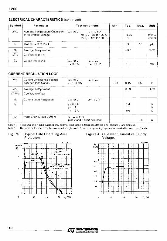
ELECTRICAL CHARACTERISTICS (Tam b = 25 °C, unless otherwise specified)
Symbol Parameter Test conditions | Min. Typ. Max. Unit
VOLTAGE REGULATION LOOP
I d Quiescent Drain Current (pin 3) V, = 20 V 4.2 9.2 mA
eN Output Noise Voltage Vo = Vref lo = 10 mA B = 1 MHz 80 mV
V0 Output Voltage Range l0 = 10 mA 2.85 36 V
AV0 Voltage Load Regulation A l0 = 2 A 0.15 1 °/o
^Vo~ (note 1) A l0 = 1.5 A 0.1 0.9 %
A V, Line Regulation < o II cn <
AVo V, = 8 to 18 V 48 60 dB
SVR Supply Voltage Rejection Vo = 5 V l0 = 500 mA AVi = 10 Vppf = 100 Hz (note 2) 48 60 dB
o
><1 Droupout Voltage between Pins 1 and 5
lo = 1.5 A AVo < 2 % 2 2.5 V
Vref Reference Voltage (pin 4) Vi = 20 V l0 = 10 mA 2.64 2.77 2.86 V
/= T SCS-THOMSON^ 7 # [RfflD(B®(ML{lCTlH3@[R0D(DS
3/9
L200
ELECTRICAL CHARACTERISTICS (continued)
Symbol Parameter Test conditions Min. Typ. Max. Unit
A V ref Average Temperature Coefficient of Reference Voltage
Vi = 20 V l0 = 10 mAfor Tj = - 25 to 125 °C for Tj = 125 to 150 °C
-0 .25-1 .5
p p
E
E
L Bias Current at Pin 4 3 10 pA
a i 4
A T T (
Average Temperature Coefficient (pin 4)
-0 .5 %rc
Z0 Output Impedance Vi = 10 V V 0 = V ref l0 = 0.5 A f = 100 Hz 1.5 mQ
CURRENT REGULATION LOOP
V sc Current Limit Sense Voltage V| = 10 V Vo = Vrefbetween Pins 5 and 2 Is = 100 mA 0 .3 8 0.45 0.52 V
A V s c Average Temperature 0 .0 3 %/°C
A T ’ V s c Coefficient of V sc
Alo Current Load Regulation Vi = 10 V A V 0 = 3 V
“ T T l0 = 0.5 A 1.4 %
lo = 1 A 1 °/o
l0 = 1.5 A 0.9 °/o
Isc Peak Short Circuit Current V i-V 0= 14 V(pins 2 and 5 short circuited) 3 .6 A
Note 1 : A load step of 2 A can be applied provided that input-output differential voltage is lower than 20 V (see Figure 3).Note 2 : The same performance can be maintained at higher output levels if a bypassing capacitor is provided between pins 2 and 4.
Figure 3 : Typical Safe Operating Area Protection.
G- 2851
Figure 4 : Quiescent Current vs. Supply Voltage.
0 10 20 30 vs (V)
4/9 r z z SGS-THOMSON^ 7# * i@ iL [lO T ® K S

L200
Figure 5 : Quiescent Current vs. Junction Voltage.
Figure 6 : Quiescent Current vs. Output Current.
0 Q4 0.8 12 1£ 2 I0 (A)
Figure 7 : Output Noise Voltage vs. Output Voltage.
Figure 8 : Output Noise Voltage vs. Frequency.
Figure 9 : Reference Voltage vs. Junction Temperature.
Figure 10 : Voltage Load Regulation vs. Junction Temperature.
SGS-THOMSON^ 7# (MOtgMIlLiOTMeS
5/9

L200
Figure 11 : Supply Voltage Rejection vs. Frequency.
O- 2849/2
Figure 13 : Output Impedance vs. Frequency.
Figure 15 : Voltage Transient Response.
Figure 12 : Dropout Voltage vs. Junction Temperature.
Figure 14 : Output Impedance vs. Output Current.
0 0.5 1 1.5 Io (A)
Figure 16 : Load Transient Response.
I0 = 1A T\j
Vj = 10V
Io=10mA to lA
A V 2 8 0 m VAVo =200mV rA C o -1
V
1|JS 1 IS
----------CQ= 0.0A7^jF
S - 2386/11JLIS
^ 7SGS-THOMSON6/9

Figure 17 : Load Transient Response.
L200
Figure 18 : Current Limit Sense Voltage vs. Junction Temperature.
APPLICATION CIRCUITS
Figure 19 : Programmable Voltage Regulator. Figure 20 : P.C. Board and ComponentsLayout of Figure 19.
Figure 21 : High Current Voltage Regulator Figure 22 : Digitally Selected Regulator withwith Short Circuit Protection. Inhibit.
fZ T SGS-THOMSON^ 7 # M(g[f?®IHiOTMO(gS
7/9

L200
Figure 23 : Programmable Voltage and Current Regulator.
Note Connecting point A to a negative voltage (for example - 3 V/10 mA) it is possible to extend the output voltage range down to 0 V and to obtain the current limiting down to this level (output short-circuit condition).
Figure 24 : High Current Regulator with NPN Pass Transistor.
Figure 25 : High Current Tracking Regulator.
SGS-THOMSON^7#
8/9
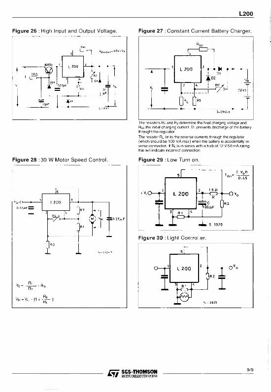
L200
Figure 26 : High Input and Output Voltage. Figure 27 : Constant Current Battery Charger.
(12V) ]I
JThe resistors Ri and R2 determine the final charging voltage and Rsc the initial charging current. D1 prevents discharge of the battery throught the regulator.The resistor Rl limits the reverse currents through the regulator (which should be 100 mA max) when the battery is accidentally reverse connected. If Rl is in series with a bulb of 12 V/50 mA rating this will indicate incorrect connection.
Figure 28 :30 W Motor Speed Control. Figure 29 : Low Turn on.
fZ T SGS-THOMSON^ 7 # M OtMiLiiOMres
9/9