qud 2-input nand gate - ik · pdf fileserial interface provides connection with...
TRANSCRIPT
TECHNICAL DATA
1 May 2012, Ver. 03
LED Driver IC Description
The IK2108A are anode-grid LED display drives 5.0V~18.0V with output size – 8 digits x 14 segments to 12 digits x 10 segments and addition key scan function. Serial interface provides connection with microprocessor.
Features
• Operation voltage for digital part: 3.0V ~ 5.5V • Operation voltage for output LEDs: 5.0V ~ 18.0V • 7-step individual dimming control for each grid • OSC: built in (with external resistor) 500kHz @ R=12.1kΩ • Pulse segment current: 27mA @ 8 digits x 14 segments 39mA @ 12 digits x 10 segments • Key scanning: 10x3 matrix • Serial Interface
• Operation Temperature : -40 ~ 85°C
Application
SOP-32
LQFP-32
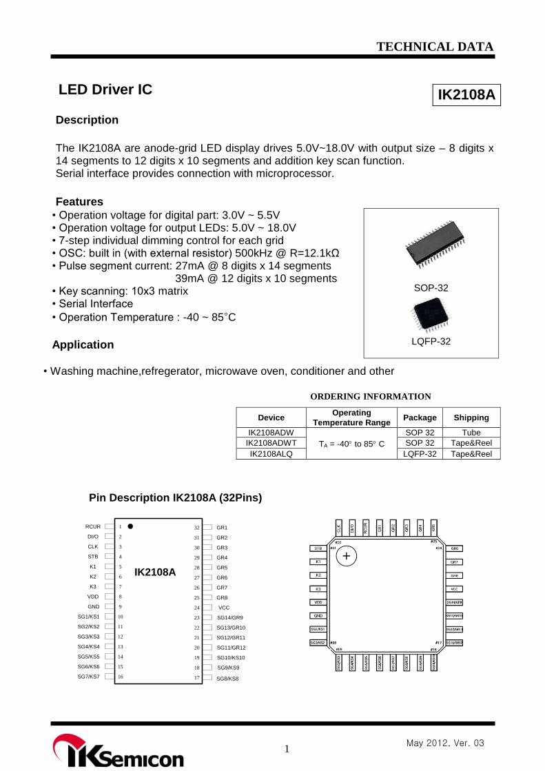
Pin Description IK2108A (32Pins)
1RCUR
DI/O
CLK
STB
K1
K2
VDD
SG1/KS1
GND
GR1
IK2108A
2
3
4
5
6
7
8
9
10
11
12
13
14
15
16
32
31
30
29
28
27
26
25
24
23
22
21
20
19
18
17
K3
SG2/KS2
SG3/KS3
SG4/KS4
SG5/KS5
SG6/KS6
SG7/KS7 SG8/KS8
SG10/KS10
SG9/KS9
SG11/GR12
SG12/GR11
SG13/GR10
SG14/GR9
VCC
GR2
GR3
GR4
GR5
GR6
GR7
GR8
IK2108A
• Washing machine,refregerator, microwave oven, conditioner and other
ORDERING INFORMATION
Device Operating
Temperature Range Package Shipping
IK2108ADW
TA = -40 to 85 C
SOP 32 Tube
IK2108ADWT SOP 32 Tape&Reel
IK2108ALQ LQFP-32 Tape&Reel
IK2108A
2 May 2012, Ver. 03
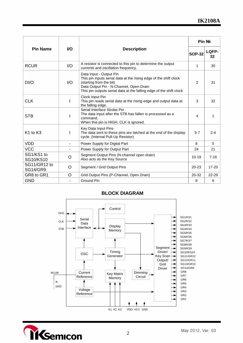
Pin Name I/O Description
Pin
SOP-32 LQFP-
32
RCUR I/O A resistor is connected to this pin to determine the output currents and oscillation frequency.
1 30
DI/O I/O
Data Input - Output Pin This pin inputs serial data at the rising edge of the shift clock (starting from the bit) Data Output Pin - N-Channel, Open-Drain This pin outputs serial data at the falling edge of the shift clock
2 31
CLK I Clock Input Pin This pin reads serial data at the rising edge and output data at the falling edge.
3 32
STB I
Serial Interface Strobe Pin The data input after the STB has fallen is processed as a command. When this pin is HIGH, CLK is ignored.
4 1
K1 to K3 I Key Data Input Pins The data sent to these pins are latched at the end of the display cycle. (Internal Pull-Up Resistor)
5-7 2-4
VDD - Power Supply for Digital Part 8 5
VCC - Power Supply for Output Part 24 21
SG1/KS1 to SG10/KS10
O Segment Output Pins (N-channel open drain) Also acts as the Key Source
10-19 7-16
SG11/GR12 to SG14/GR9
O Segment / Grid Output Pins 20-23 17-20
GR8 to GR1 O Grid Output Pins (P-Channel, Open Drain) 25-32 22-29
GND - Ground Pin 9 6
BLOCK DIAGRAM
Serial
Data
Interface
OSC
Display
Memory
Control
Timing
Generator
Key Matrix
Memory
Current
Reference
Voltage
Reference
Dimming
Circuit
Segment
Driver/
Key Scan
Output/
Grid
Driver
GR1
GR2
GR3
GR4
GR5
GR6
GR7
GR8
SG10/KS10
SG9/KS9
SG11/GR12
SG12/GR11
SG13/GR10
SG14/GR9
SG1/KS1
SG2/KS2
SG3/KS3
SG4/KS4
SG5/KS5
SG6/KS6
SG7/KS7
SG8/KS8
GNDVCCVDDK1 K2 K3
R
GND
RCUR
DI/O
CLK
STB
IK2108A
3 May 2012, Ver. 03
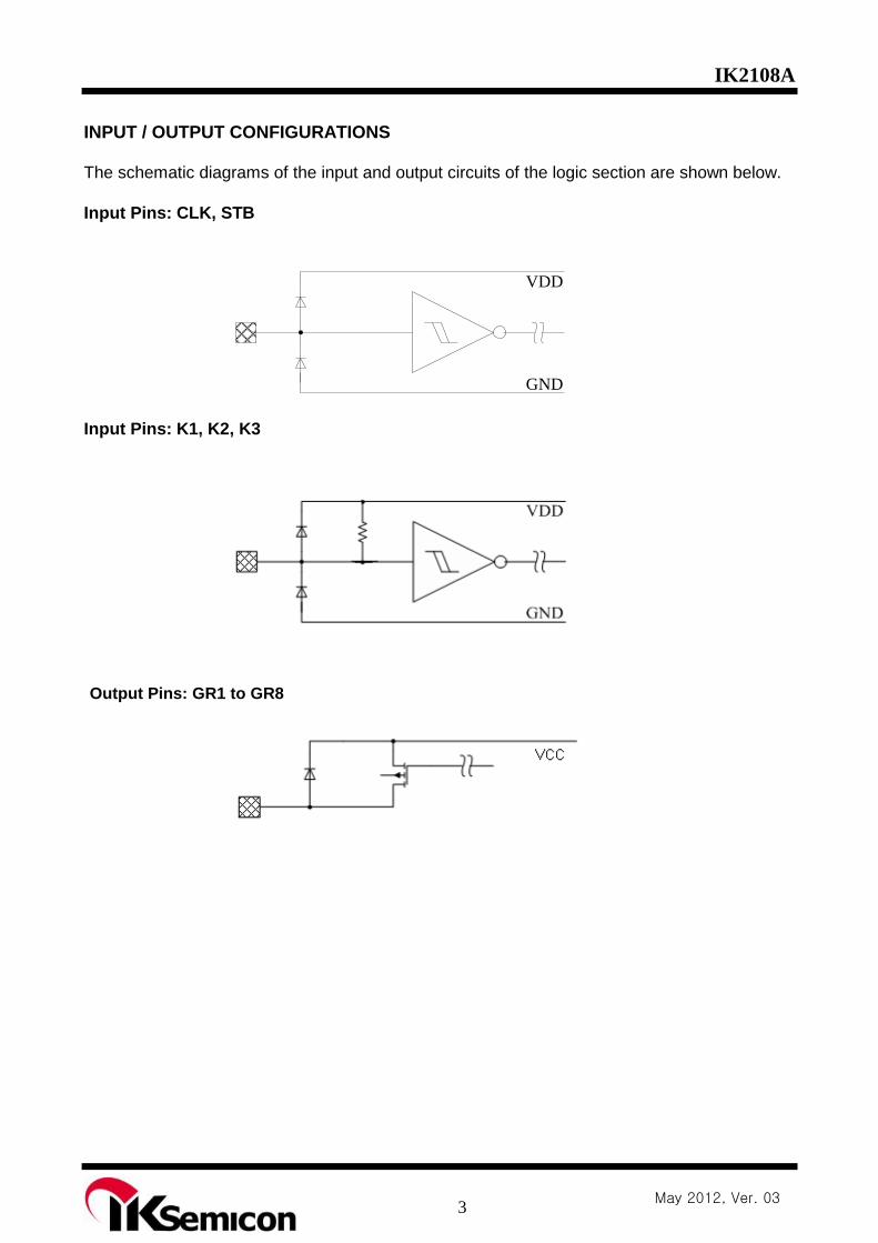
INPUT / OUTPUT CONFIGURATIONS
The schematic diagrams of the input and output circuits of the logic section are shown below.
Input Pins: CLK, STB
Input Pins: K1, K2, K3
Output Pins: GR1 to GR8
VDD
GND
IK2108A
4 May 2012, Ver. 03
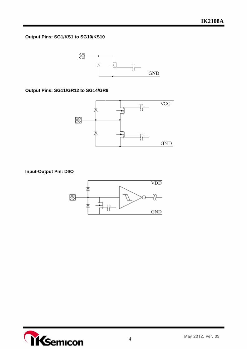
Output Pins: SG1/KS1 to SG10/KS10
Output Pins: SG11/GR12 to SG14/GR9
Input-Output Pin: DI/O
GND
IK2108A
5 May 2012, Ver. 03
FUNCTIONAL DESCRIPTION
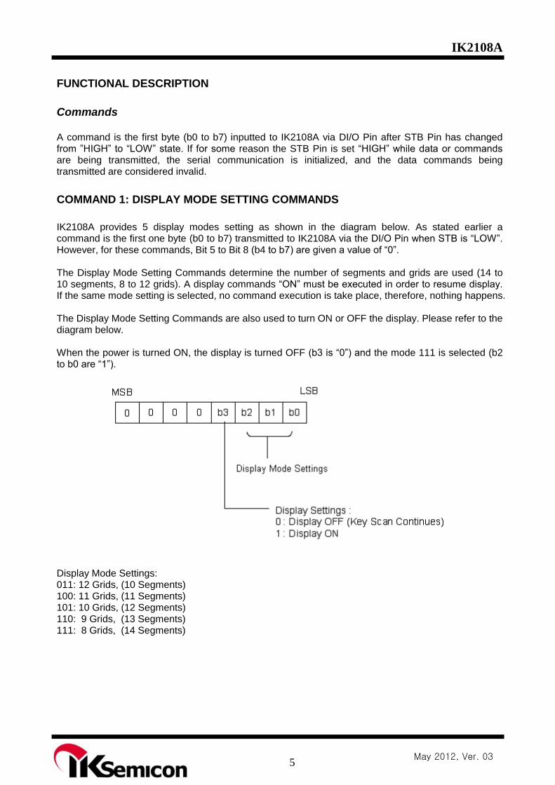
Commands A command is the first byte (b0 to b7) inputted to IK2108A via DI/O Pin after STB Pin has changed from ”HIGH” to “LOW” state. If for some reason the STB Pin is set “HIGH” while data or commands are being transmitted, the serial communication is initialized, and the data commands being transmitted are considered invalid.
COMMAND 1: DISPLAY MODE SETTING COMMANDS
IK2108A provides 5 display modes setting as shown in the diagram below. As stated earlier a command is the first one byte (b0 to b7) transmitted to IK2108A via the DI/O Pin when STB is “LOW”. However, for these commands, Bit 5 to Bit 8 (b4 to b7) are given a value of “0”. The Display Mode Setting Commands determine the number of segments and grids are used (14 to 10 segments, 8 to 12 grids). A display commands “ON” must be executed in order to resume display. If the same mode setting is selected, no command execution is take place, therefore, nothing happens. The Display Mode Setting Commands are also used to turn ON or OFF the display. Please refer to the diagram below. When the power is turned ON, the display is turned OFF (b3 is “0”) and the mode 111 is selected (b2 to b0 are “1”).
Display Mode Settings: 011: 12 Grids, (10 Segments) 100: 11 Grids, (11 Segments) 101: 10 Grids, (12 Segments) 110: 9 Grids, (13 Segments) 111: 8 Grids, (14 Segments)
IK2108A
6 May 2012, Ver. 03
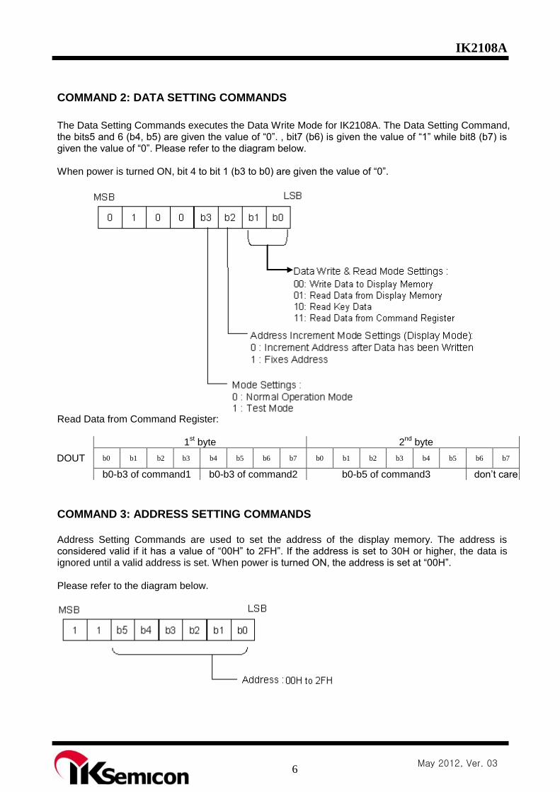
COMMAND 2: DATA SETTING COMMANDS
The Data Setting Commands executes the Data Write Mode for IK2108A. The Data Setting Command, the bits5 and 6 (b4, b5) are given the value of “0”. , bit7 (b6) is given the value of “1” while bit8 (b7) is given the value of “0”. Please refer to the diagram below. When power is turned ON, bit 4 to bit 1 (b3 to b0) are given the value of “0”.
Read Data from Command Register:
DOUT
1st byte 2
nd byte
b0 b1 b2 b3 b4 b5 b6 b7 b0 b1 b2 b3 b4 b5 b6 b7
b0-b3 of command1 b0-b3 of command2 b0-b5 of command3 don’t care
COMMAND 3: ADDRESS SETTING COMMANDS
Address Setting Commands are used to set the address of the display memory. The address is considered valid if it has a value of “00H” to 2FH”. If the address is set to 30H or higher, the data is ignored until a valid address is set. When power is turned ON, the address is set at “00H”. Please refer to the diagram below.
IK2108A
7 May 2012, Ver. 03
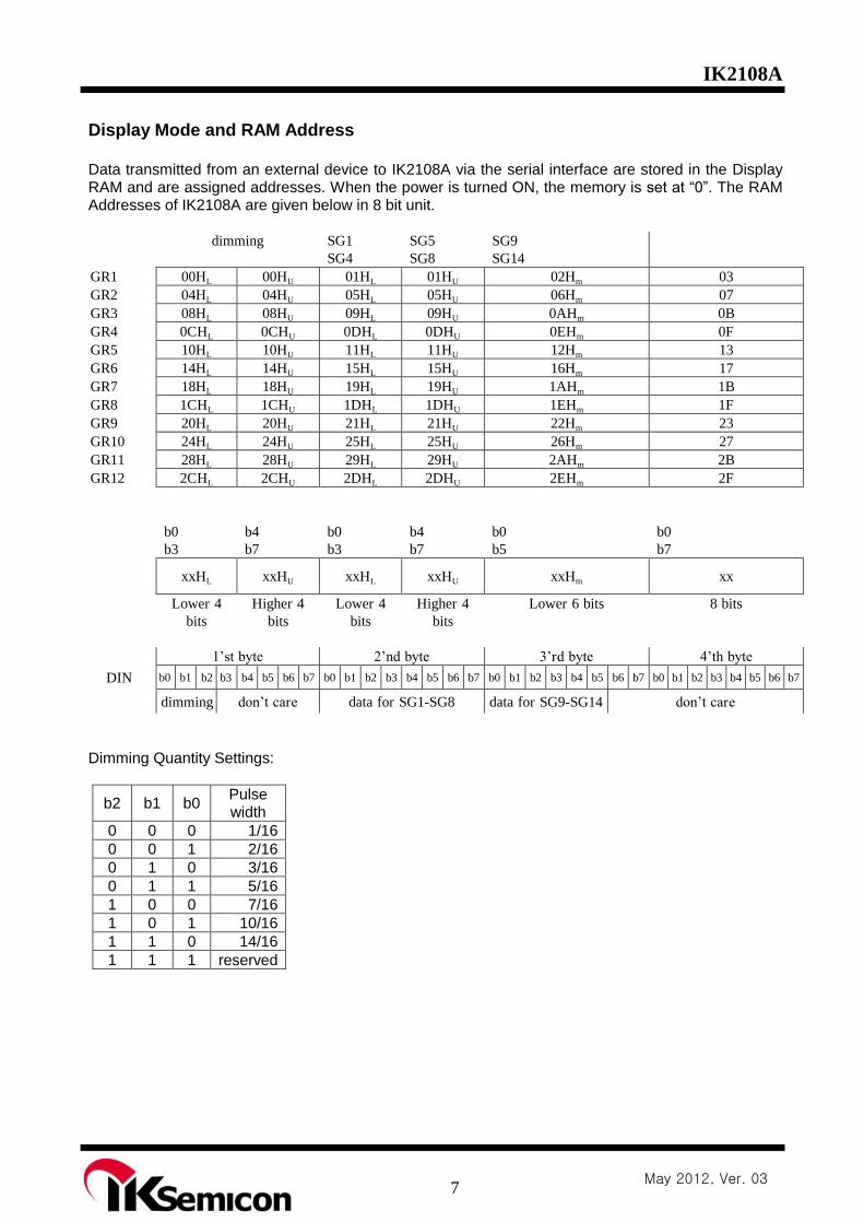
Display Mode and RAM Address
Data transmitted from an external device to IK2108A via the serial interface are stored in the Display RAM and are assigned addresses. When the power is turned ON, the memory is set at “0”. The RAM Addresses of IK2108A are given below in 8 bit unit. dimming SG1
SG4
SG5
SG8
SG9
SG14
GR1 00HL 00HU 01HL 01HU 02Hm 03
GR2 04HL 04HU 05HL 05HU 06Hm 07
GR3 08HL 08HU 09HL 09HU 0AHm 0B
GR4 0CHL 0CHU 0DHL 0DHU 0EHm 0F
GR5 10HL 10HU 11HL 11HU 12Hm 13
GR6 14HL 14HU 15HL 15HU 16Hm 17
GR7 18HL 18HU 19HL 19HU 1AHm 1B
GR8 1CHL 1CHU 1DHL 1DHU 1EHm 1F
GR9 20HL 20HU 21HL 21HU 22Hm 23
GR10 24HL 24HU 25HL 25HU 26Hm 27
GR11 28HL 28HU 29HL 29HU 2AHm 2B
GR12 2CHL 2CHU 2DHL 2DHU 2EHm 2F
b0
b3
b4
b7
b0
b3
b4
b7
b0
b5
b0
b7
xxHL xxHU xxHL xxHU xxHm xx
Lower 4
bits
Higher 4
bits
Lower 4
bits
Higher 4
bits
Lower 6 bits 8 bits
1’st byte 2’nd byte 3’rd byte 4’th byte
DIN b0 b1 b2 b3 b4 b5 b6 b7 b0 b1 b2 b3 b4 b5 b6 b7 b0 b1 b2 b3 b4 b5 b6 b7 b0 b1 b2 b3 b4 b5 b6 b7
dimming don’t care data for SG1-SG8 data for SG9-SG14 don’t care
Dimming Quantity Settings:
b2 b1 b0 Pulse width
0 0 0 1/16
0 0 1 2/16
0 1 0 3/16
0 1 1 5/16
1 0 0 7/16
1 0 1 10/16
1 1 0 14/16
1 1 1 reserved
IK2108A
8 May 2012, Ver. 03
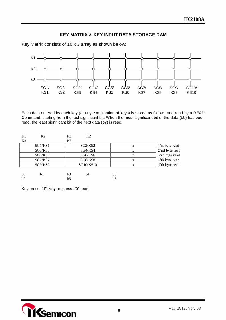
KEY MATRIX & KEY INPUT DATA STORAGE RAM
Key Matrix consists of 10 x 3 array as shown below:
K1
K2
K3
SG1/
KS1
SG2/
KS2
SG3/
KS3
SG4/
KS4
SG5/
KS5
SG6/
KS6
SG7/
KS7
SG8/
KS8
SG9/
KS9
SG10/
KS10
Each data entered by each key (or any combination of keys) is stored as follows and read by a READ Command, starting from the last significant bit. When the most significant bit of the data (b0) has been read, the least significant bit of the next data (b7) is read. K1 K2
K3
K1 K2
K3
SG1/KS1 SG2/KS2 x 1’st byte read
SG3/KS3 SG4/KS4 x 2’nd byte read
SG5/KS5 SG6/KS6 x 3’rd byte read
SG7/KS7 SG8/KS8 x 4’th byte read
SG9/KS9 SG10/KS10 x 5’th byte read
b0 b1
b2
b3 b4
b5
b6
b7
Key press=”1”, Key no press=”0” read.
IK2108A
9 May 2012, Ver. 03
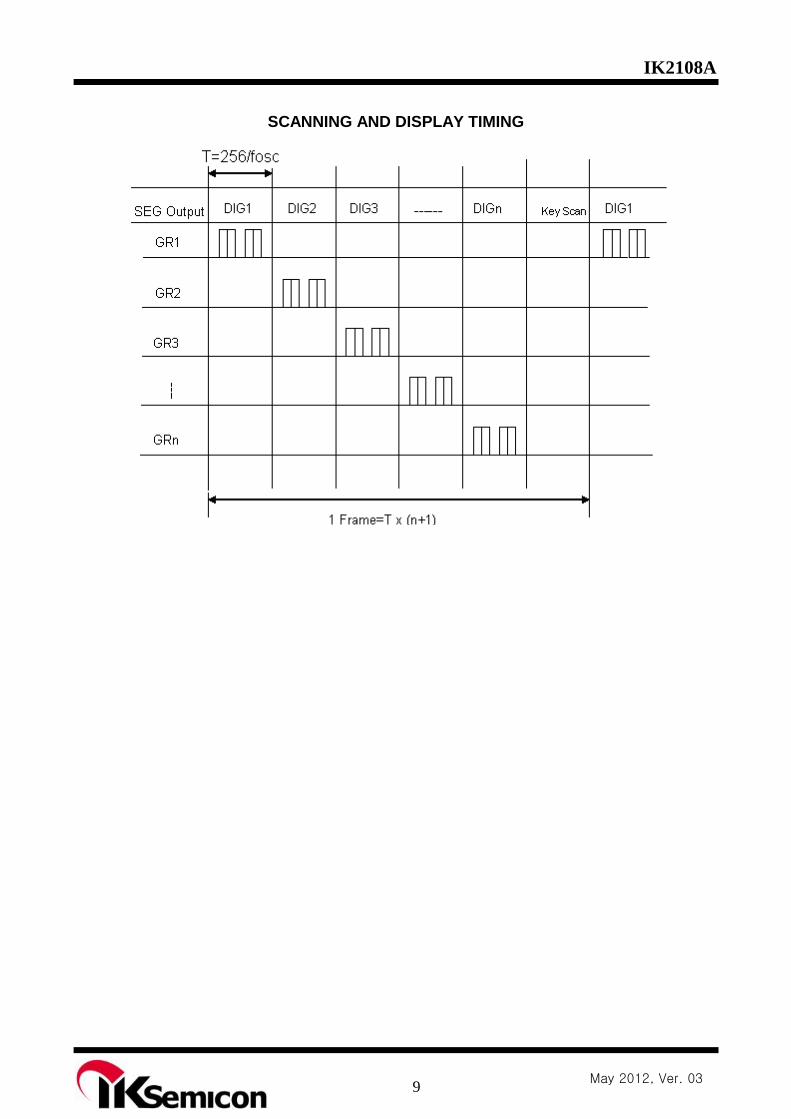
SCANNING AND DISPLAY TIMING
IK2108A
10 May 2012, Ver. 03
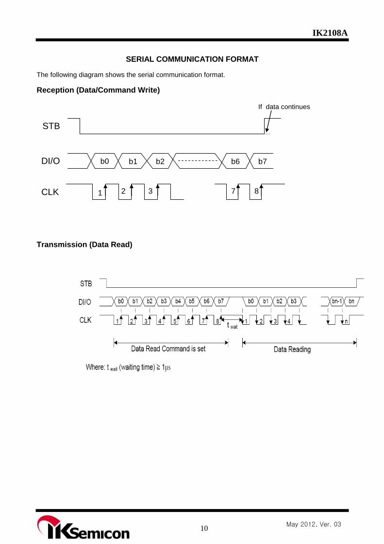
SERIAL COMMUNICATION FORMAT
The following diagram shows the serial communication format.
Reception (Data/Command Write)
Transmission (Data Read)
STB
DI/O
CLK
1 2 3 7 8
If data continues
b0 b1 b2 b6 b7
IK2108A
11 May 2012, Ver. 03
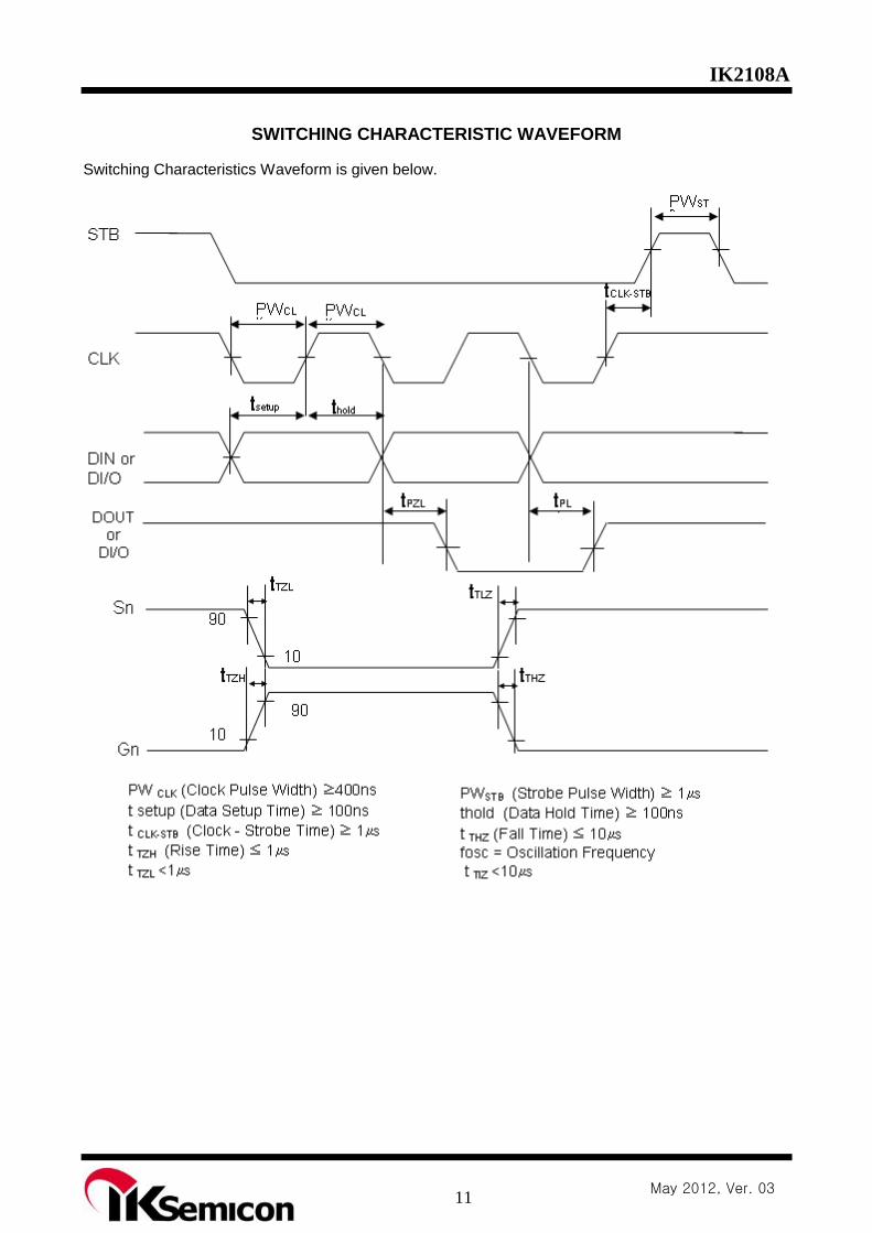
SWITCHING CHARACTERISTIC WAVEFORM
Switching Characteristics Waveform is given below.
IK2108A
12 May 2012, Ver. 03
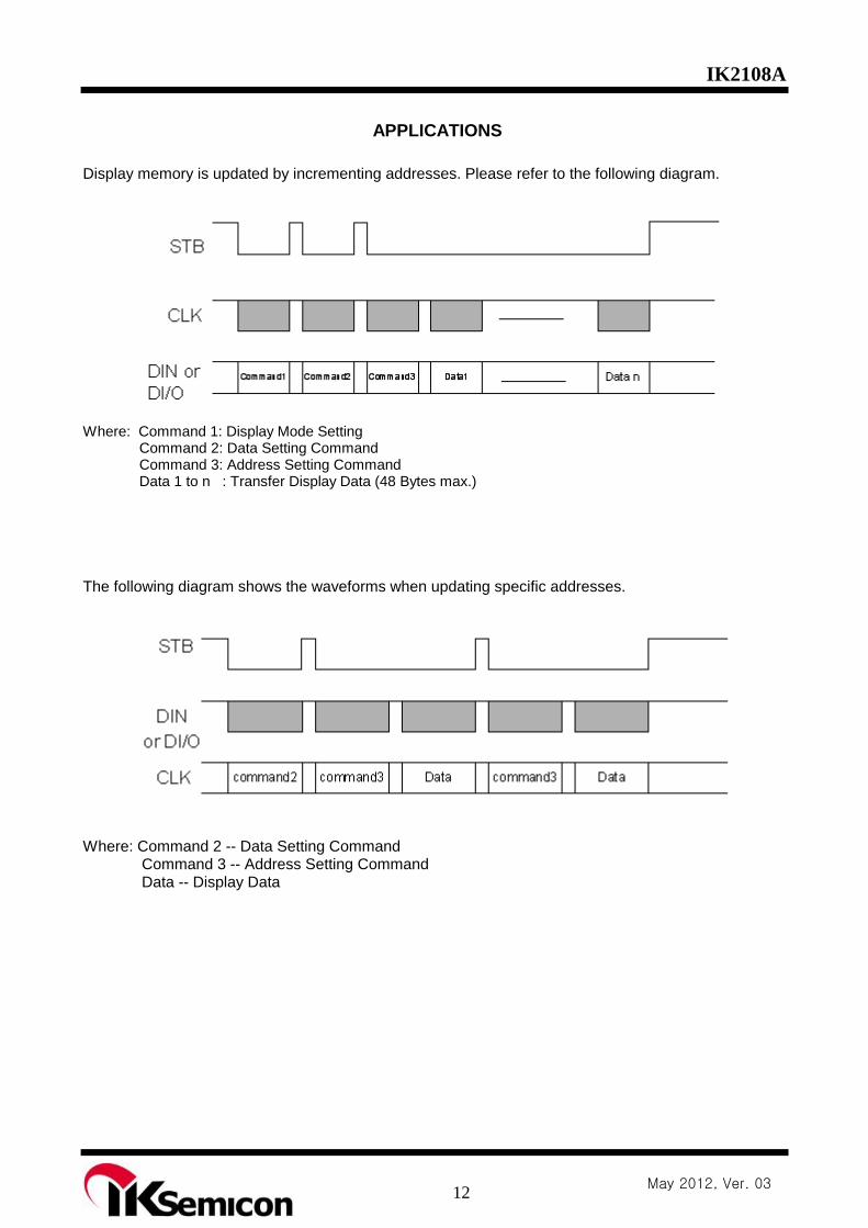
APPLICATIONS
Display memory is updated by incrementing addresses. Please refer to the following diagram.
Where: Command 1: Display Mode Setting Command 2: Data Setting Command Command 3: Address Setting Command Data 1 to n : Transfer Display Data (48 Bytes max.)
The following diagram shows the waveforms when updating specific addresses.
Where: Command 2 -- Data Setting Command Command 3 -- Address Setting Command Data -- Display Data
IK2108A
13 May 2012, Ver. 03
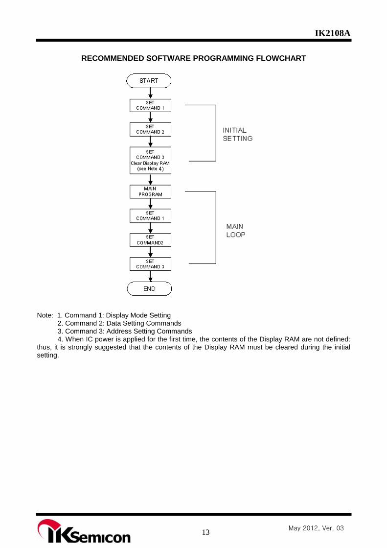
RECOMMENDED SOFTWARE PROGRAMMING FLOWCHART
Note: 1. Command 1: Display Mode Setting 2. Command 2: Data Setting Commands 3. Command 3: Address Setting Commands 4. When IC power is applied for the first time, the contents of the Display RAM are not defined: thus, it is strongly suggested that the contents of the Display RAM must be cleared during the initial setting.
IK2108A
14 May 2012, Ver. 03
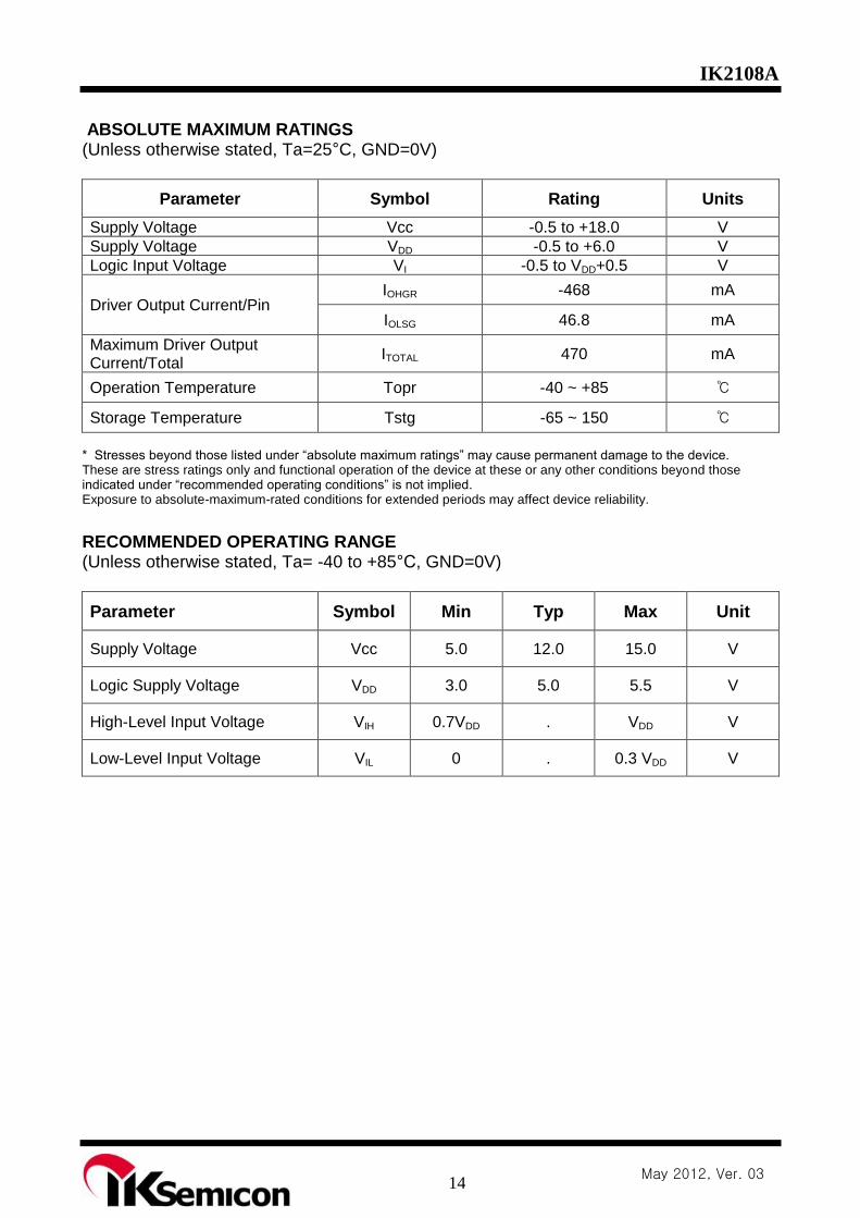
ABSOLUTE MAXIMUM RATINGS (Unless otherwise stated, Ta=25°C, GND=0V)
Parameter Symbol Rating Units
Supply Voltage Vcc -0.5 to +18.0 V
Supply Voltage VDD -0.5 to +6.0 V
Logic Input Voltage VI -0.5 to VDD+0.5 V
Driver Output Current/Pin IOHGR -468 mA
IOLSG 46.8 mA
Maximum Driver Output Current/Total
ITOTAL 470 mA
Operation Temperature Topr -40 ~ +85
Storage Temperature Tstg -65 ~ 150
* Stresses beyond those listed under “absolute maximum ratings” may cause permanent damage to the device. These are stress ratings only and functional operation of the device at these or any other conditions beyond those indicated under “recommended operating conditions” is not implied. Exposure to absolute-maximum-rated conditions for extended periods may affect device reliability.
RECOMMENDED OPERATING RANGE (Unless otherwise stated, Ta= -40 to +85°C, GND=0V)
Parameter Symbol Min Typ Max Unit
Supply Voltage Vcc 5.0 12.0 15.0 V
Logic Supply Voltage VDD 3.0 5.0 5.5 V
High-Level Input Voltage VIH 0.7VDD . VDD V
Low-Level Input Voltage VIL 0 . 0.3 VDD V
IK2108A
15 May 2012, Ver. 03
ELECTRICAL CHARACTERISTICS (Unless otherwise stated, Vcc=5.0~18.0V, VDD=3.3~5.5V, GND=0V, Ta=-40 ~ 85°C)
Parameter Symbol Test Condition Min Typ Max Unit
Low-Level Output Current
IOLSG
Vo=1.0V SG1/KS1 to SG10/KS10
SG11/GR12 to SG14/GR9 display 8digitsx14segments
21.6 27 32.4
mA
Vo=0.9V SG1/KS1 to SG10/KS10
display 12digitsx10segments 31.2 39 46.8
High-Level Output Current
IOHGR
Vo=Vcc-1.0V R = 12.1KOhm
GR1 to GR8
display 8digitsx14segments
-302.4 -378 -453.6
mA Vo=Vcc-1.1V R = 12.1KOhm
GR1 to GR8
SG11/GR12 to SG14/GR9 display 12digitsx10segments
-312 -390 -468
Dynamic Current IDDdyn - - - 1.2 mA
Digital Input Current
IDG - -1 - +1 uA
Low-Level Digital Output Current
IOLDOUT VO = 0.4V
DOUT 4 - - mA
Segment Low-Level Output Current Tolerance
ITOLSG
Vo=1.0V SG1/KS1 to SG10/KS10
SG11/GR12 to SG14/GR9 display 8digitsx14segments
- - ±5
%
Vo=0.9V SG1/KS1 to SG10/KS10
display 12digitsx10segments - - ±5
High-Level Input Voltage for DI/O
VIH - 0.7VDD - VDD V
Low-Level Input Voltage for DI/O
VIL - 0 - 0.3VDD V
Oscillation Frequency
fOSC (VDD=3.3 ~5.5V) R = 12.1kOhm
400 500 600 kHz
K1 to K3 Pull Up Resistor
RPU K1 to K3
VDD =5.0V 22.5 30.0 37.5 KΩ
IK2108A
16 May 2012, Ver. 03
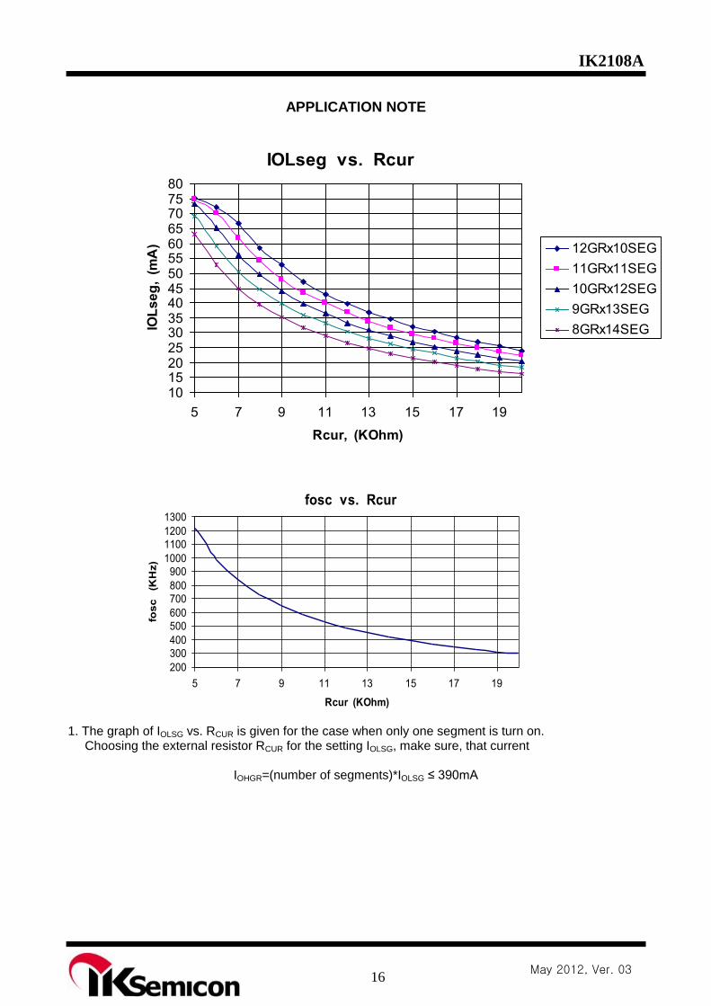
APPLICATION NOTE
IOLseg vs. Rcur
101520253035404550556065707580
5 7 9 11 13 15 17 19
Rcur, (KOhm)
IOL
se
g, (
mA
) 12GRx10SEG
11GRx11SEG
10GRx12SEG
9GRx13SEG
8GRx14SEG
fosc vs. Rcur
200
300
400
500
600
700
800
900
1000
1100
1200
1300
5 7 9 11 13 15 17 19
Rcur (KOhm)
fos
c (
KH
z)
1. The graph of IOLSG vs. RCUR is given for the case when only one segment is turn on.
Choosing the external resistor RCUR for the setting IOLSG, make sure, that current
IOHGR=(number of segments)*IOLSG ≤ 390mA
IK2108A
17 May 2012, Ver. 03
2. The cell of Display Memory has a dead time zone. If the software program is not correct, it is
possible the blinking of display. The blinking frequency for the single segment is:
)*5.01(*256
2
CLK
OSCCOMMANDMAX
BLINKF
F
G
FF , (less value is better),
where 2COMMANDF – frequency of the use of the command2 (Write Data to Display Memory);
G– number of grids in used mode;
OSCF – frequency of internal OSC;
CLKF – clock frequency.
So, main rule for update the Display Memory is do it if it really need. Don’t do it continually with
high speed, but if it something like movie you can. Or another way is turn off the display while the command of Write Data to Display Memory is executed.
3. To determine the Average Consumption Current of IK2108A, you should use the next formula (the
current value during key scan period is ignored as this value is very small in compare with segment’s current):
Itotal(avrg) = (N* IOLSG *Dimming)*(M/(M+1)),
where N is segment’s number;
M is grid’s number;
Dimming is Dimming value (see p.7);
IOLSG is output segment’s current (see table Electrical Characteristics).
Therefore different display configurations will have different current consumption. Let’s consider the maximum case, when Dimming is 14/16 and all segments and grids are used:
8 grids x 14 segments display: Itotal(avrg)=(14*27mA(typical value)*14/16)*(8/9)=294mA;
12 grids x 10 segments display: Itotal(avrg)=(10*39mA(typical value)*14/16)*(12/13)=315mA.
IK2108A
18 May 2012, Ver. 03
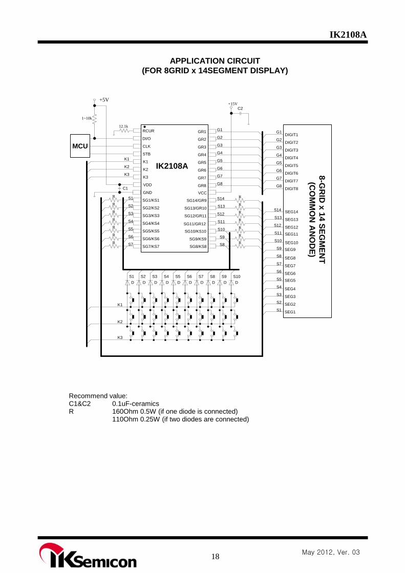
APPLICATION CIRCUIT
(FOR 8GRID x 14SEGMENT DISPLAY)
RCUR
DI/O
CLK
STB
K1
K2
VDD
SG1/KS1
GND
GR1
IK2108A
K3
SG2/KS2
SG3/KS3
SG4/KS4
SG5/KS5
SG6/KS6
SG7/KS7 SG8/KS8
SG10/KS10
SG9/KS9
SG11/GR12
SG12/GR11
SG13/GR10
SG14/GR9
VCC
GR2
GR3
GR4
GR5
GR6
GR7
GR8
12.1k
MCU
1~10k
+5V
S1 S2 S3 S4 S5 S6 S7 S8 S9 S10
K1
K2
K3
S1
S2
S3
S4
S5
S6
S7 S8
S14
S13
S12
S11
S10
S9
G1
G2
G3
G4
G5
G6
G7
G8
R
R
R
R
R
R
R
R
R
R
R
R
R
K1
K2
K3
+15VC2
C1
G1
G2
G3
G4
G5
G6
G7
G8
DIGIT1
DIGIT2
DIGIT3
DIGIT4
DIGIT5
DIGIT6
DIGIT7
DIGIT8
S14
S13
S12
S11
S10
S9
S1
S2
S3
S4
S5
S6
S7
S8
SEG14
SEG13
SEG12
SEG11
SEG10
SEG9
SEG8
SEG7
SEG6
SEG5
SEG4
SEG3
SEG2
SEG1
8-G
RID
x 1
4 S
EG
ME
NT
(CO
MM
ON
AN
OD
E)
D D D D D D D D D D
R
Recommend value: C1&C2 0.1uF-ceramics R 160Ohm 0.5W (if one diode is connected) 110Ohm 0.25W (if two diodes are connected)
IK2108A
19 May 2012, Ver. 03
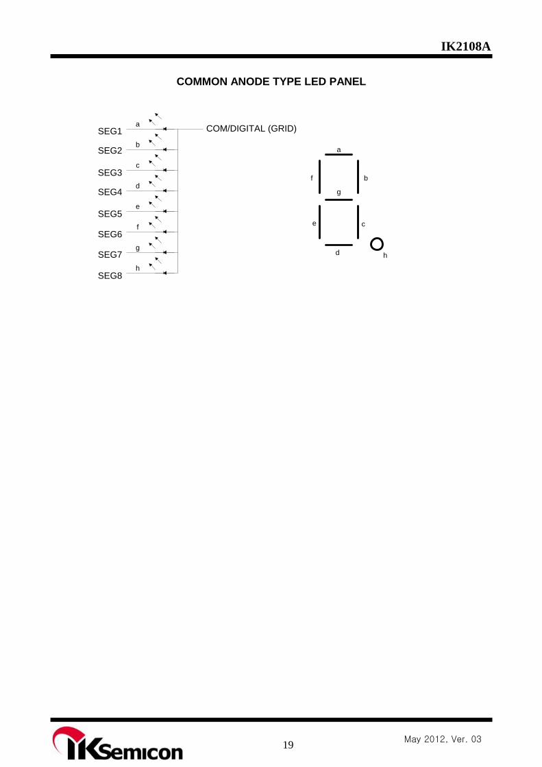
COMMON ANODE TYPE LED PANEL
COM/DIGITAL (GRID)SEG1
SEG2
SEG3
SEG4
SEG5
SEG6
SEG7
SEG8
a
b
c
d
e
f
g
h
a
b
c
d
e
f
g
h
IK2108A
20 May 2012, Ver. 03
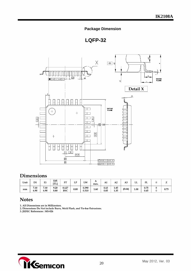
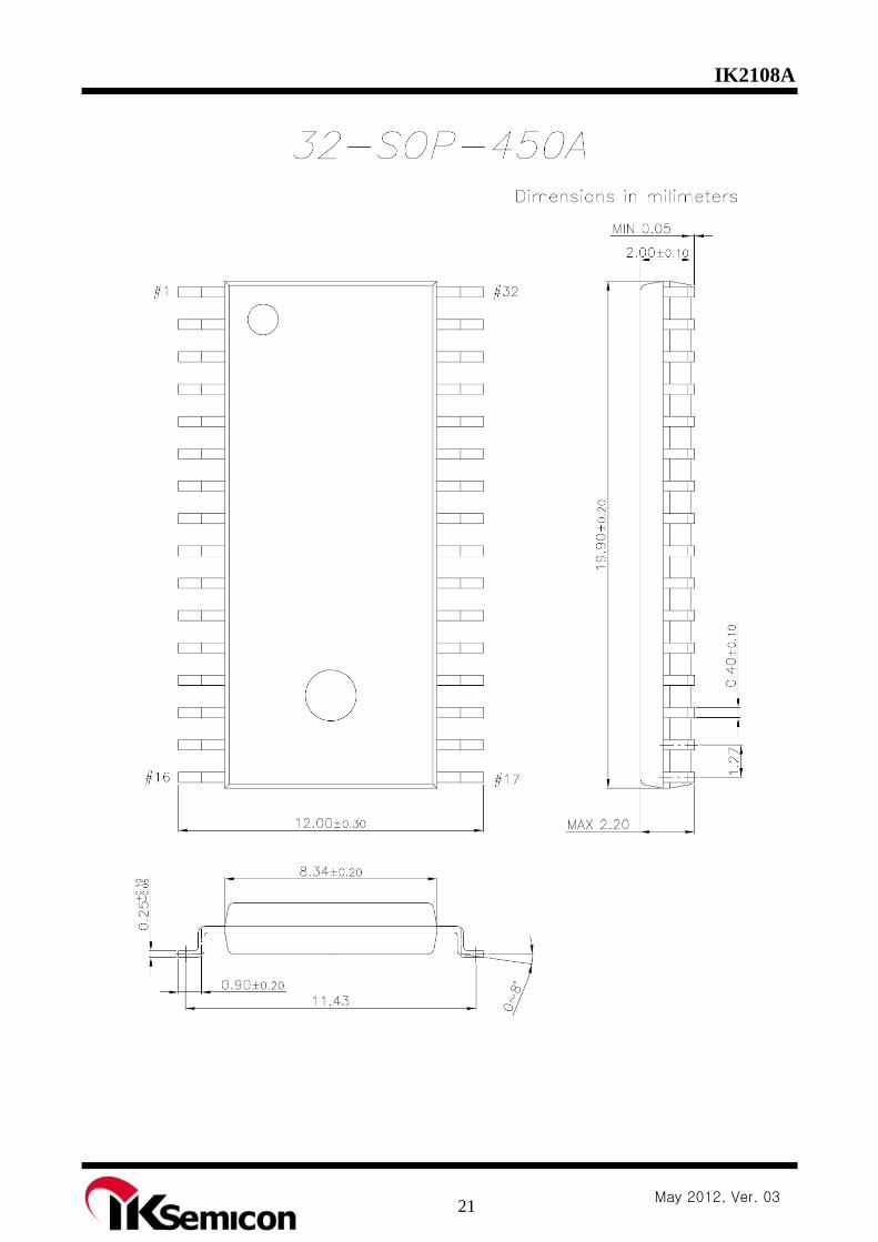
Package Dimension
LQFP-32
IK2108A
21 May 2012, Ver. 03