qn908x crystals load capacitance calibration · an12104 qn908x crystals load capacitance...
TRANSCRIPT

AN12104 QN908x Crystals Load Capacitance Calibration
Rev. 2.1 — 04 June 2018 Application note
Document information
Info Content
Keywords QN908x, BLE, BTLE, Crystal oscillator, Calibration, Load Capacitance,
Bluetooth Smart
Abstract This Application note describes in brief the calibration of high frequency
(16 MHz/32 MHz) and low frequency (32.768 kHz) crystals. The terms
BLE, BTLE and Bluetooth Smart will be used interchangeably

NXP Semiconductors AN12104 QN908x Crystals Load Capacitance Calibration
AN12104 All information provided in this document is subject to legal disclaimers. © NXP Semiconductors N.V.2018. All rights reserved.
Application note Rev 2.1 — 04 June 2018 2 of 12
Contact information
For more information, please visit: http://www.nxp.com
Revision history
Rev Date Description
1.0 2017/12/22 QN908x Crystals Load Capacitance Calibration initial version.
2.0 2018/02/21 Added description to get the binary file hci_black_box.bin, added indicator on where to
setup the connection with QN9080 DK.
2.1 2018/06/04 Minor edits.

NXP Semiconductors AN12104 QN908x Crystals Load Capacitance Calibration
AN12104 All information provided in this document is subject to legal disclaimers. © NXP Semiconductors N.V.2018. All rights reserved.
Application note Rev 2.1 — 04 June 2018 3 of 12
1. Introduction
QN908x is designed with no load capacitors needed for both 16 MHz/32 MHz and 32.768 kHz crystal oscillators, the load capacitor is integrated inside chips to reduce the BOM cost without affecting the crystal accuracy. An accurate crystal oscillator results in better RF performance. The 16 MHz/32 MHz crystal circuitry decides the performance of the RF peripheral, while the 32.768 kHz crystal circuitry decides the accuracy of RTC and the power consumption of BLE connection. As part of the crystal circuitry, the load capacitance is crucial to the accuracy of clock from the crystal oscillator.
2. Load Capacitance Parameters
QN908x is integrated with load capacitance for both high and low frequency crystals.
2.1 Registers for Load Capacitance Configuration The value of load capacitance is configured by registers. For high frequency crystal, the bits 22 to 28 of register ANA_CTRL0 is used for setting load capacitance. Refer to table 1 below for details. Table 1. ANA_CTRL0
Bit Symbol Access Reset
value
Description
27:22 XTAL_LOAD_C
AP
RW 0x20 register-controlled load cap of the XTAL in
normal mode. XTAL load cap =5 pF + 0.35 pF
XTAL_LOAD_CAP + 5 pF
XTAL_EXTRA_CAP
28 XTAL_EXTRA_
CAP
RW 0x0 add extra 16/32 MHz XTAL load cap
For low frequency crystal, the bits 8 to 14 of register XTAL32K_CTRL is used for setting load capacitance. Refer to table 2 below for details. Table 2. XTAL32K_CTRL
Bit Symbol Access Reset
value
Description
13:8 XTAL32K_LOA
D_CAP
RW 0x30 load cap selection of XTAL32K; XTAL32K
load cap = 3.6 pF + 0.4 pF
XTAL32K_LOAD_CAP + 6.4 pF
XTAL32K_EXTRA_CAP
14 XTAL32K_EXT
RA_CAP
RW 0x0 add extra XTAL32K load cap or not
NXP Semiconductors AN12104 QN908x Crystals Load Capacitance Calibration
AN12104 All information provided in this document is subject to legal disclaimers. © NXP Semiconductors N.V.2018. All rights reserved.
Application note Rev 2.1 — 04 June 2018 4 of 12
2.2 Configuration Step for Load Capacitance Based on the table 1 and table 2 above, the step configurable of load capacitances is 0.35 pF and 0.4 pF respectively for high and low frequency crystals.
2.3 Extra Value for Load Capacitance To add an extra load capacitance, set the corresponding register. The extra values are 5 pF and 6.4 pF respectively for the high and low frequency crystals.
2.4 Adjustable range of Load Capacitance With the predefined step and extra value, we can get the adjusting range of load capacitance. Refer to table 3 and table 4 below for details. Table 3. High Frequency Crystal Adjustable Range of Load Capacitance
Extra addition
capacitor option
Capacitor for the crystal Capacitor pre-step for each
NO 5 pF ~ 27.05 pF 0.35 pF
YES 10 pF ~ 32.05 pF 0.35 pF
Table 4. Low Frequency Crystal Adjustable Range of Load Capacitance
Extra addition
capacitor option
Capacitor range for the crystal Capacitor pre-step for each
NO 5 pF ~ 27.05 pF 0.4 pF
YES 10 pF ~ 32.05 pF 0.4 pF
3. Typical Crystal Circuitry
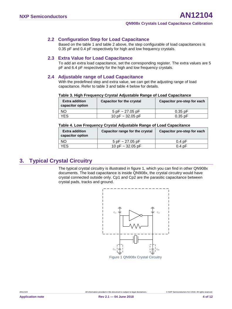
The typical crystal circuitry is illustrated in figure 1, which you can find in other QN908x documents. The load capacitance is inside QN908x, the crystal circuitry would have crystal connected outside only. Cp1 and Cp2 are the parasitic capacitance between crystal pads, tracks and ground.
CL1 CL2
CP1 CP2
Figure 1 QN908x Crystal Circuitry

NXP Semiconductors AN12104 QN908x Crystals Load Capacitance Calibration
AN12104 All information provided in this document is subject to legal disclaimers. © NXP Semiconductors N.V.2018. All rights reserved.
Application note Rev 2.1 — 04 June 2018 5 of 12
3.1 Advantages of Inside Integrated Load Capacitance
QN908x is a BLE SoC targeting wearable and fitness product, which are always cost and
size sensitive. With the on-chip capacitor feature, the design based on QN908x can save
cost and valuable PCB space.
The carrier of QN908x RF is based on the high frequency clock, the accurate load
capacitance of the high-frequency crystal can get an accurate RF signal. With the on-
chip capacitor, we can adjust the load capacitance by small step (0.35 pf) to get more
accurate RF frequency.
The RTC accuracy depends on the accuracy of the low-frequency crystal circuit. With the
on-chip adjustable load capacitance, it can get a good accuracy.
4. Fine Tuning the Load Capacitance
As described in section 3.1, the accuracy of crystal circuit has impact on the performance
of peripherals. It is necessary to fine tune it during the product design phase.
4.1 High Frequency Crystal Tuning 1) Hardware
• Spectrum Analyzer
• QN908x based DUT
• A test PC
• USB to UART cable
• Coaxial cable 2) Software tool & firmware
• Firmware: hci_black_box.bin (the project file is located in the SDK folder ...\boards\qn908xcdk\wireless_examples\bluetooth\hci_bla
ck_box, compile the project to generate the binary)
• Software tool: QN908x_CrystalCal.exe, a PC based tool.
4.1.1 Hardware Setup The 2.4 GHz TX carrier is derived from the high frequency crystal oscillator, the load capacitance is better matched if the carrier frequency is closer to the frequency the DUT intends to transmit. For measuring the frequency accuracy, the TX carrier frequency is easily measured with spectrum analyzer. The DUT can be controlled to transmit signals only after burning the binary file hci_black_box.bin. The software tool QN908x_CrystalCal.exe is running on a test PC and send commands to DUT by UART interface. The hardware setup is illustrated in figure 2 below.

NXP Semiconductors AN12104 QN908x Crystals Load Capacitance Calibration
AN12104 All information provided in this document is subject to legal disclaimers. © NXP Semiconductors N.V.2018. All rights reserved.
Application note Rev 2.1 — 04 June 2018 6 of 12
Figure 2 Hardware Setup for High Frequency Crystal Calibration
4.1.2 Firmware and Software Tool Introduction
The hci_black_box.bin is the firmware used for QN908x DTM test, as well as handling
vendor specific commands, such as Read/Write QN908x registers.
Figure 3 Crystal Calibration Tool
As illustrated in figure 2, QN908x_CrystalsCal.exe is the Windows based PC tool used
for QN908x load capacitance calibration test, which consists of controlling QN908x for
TX carrier transmission and calibration related register accessing.
4.1.3 Test Procedure
During the hardware design phase, the hardware engineer should choose the crystal
following the rules addressed in the QN908x Hardware Design Consideration Application
Note.
USB to UART cable
Coaxial cable
SMA Connection
NXP Semiconductors AN12104 QN908x Crystals Load Capacitance Calibration
AN12104 All information provided in this document is subject to legal disclaimers. © NXP Semiconductors N.V.2018. All rights reserved.
Application note Rev 2.1 — 04 June 2018 7 of 12
QN908x is shipping with default value used for setting the load capacitance value by
register ANA_CTRL0. The value is 0x08, which is a verified value for QN9080 DK. But
even the crystal is from the same vendor and with the same parameters, the load
capacitance shall be re-calibrated if PCB design/manufacturer is changed.
The test procedure for the hih-crystal load capacitance calibration test is as the following:
1. Setup the hardware connection as illustrated in figure 2.
2. Download the firmware hci_black_box.bin into QN908x.
3. Start the calibration tool QN908x_CrystalsCalc.exe.
4. Input an initial Hex value in Hex input box.
5. Click Set button in 16 MHz/32 MHz group to trigger TX carrier transmission.
6. Observe the frequency value in spectrum analyzer.
7. Adjust the value upwards if minus frequency offset found by up/down button.
8. Repeat from step 5 until the smallest offset is found.
4.2 Low Frequency Crystal Tuning 1) Hardware
• Oscilloscope
• QN908x based DUT
• A test PC
• USB to UART cable 2) Software tool & firmware
• Firmware: hci_black_box.bin (the project file located in the SDK folder ...\boards\qn908xcdk\wireless_examples\bluetooth\hci_bla
ck_box, compile the project to generate the binary)
• Software tool: QN908x_CrystalCal.exe, a PC based tool.
4.2.1 Hardware Setup The low frequency clock in QN908x is used by RTC and Sleep Timer. Aa accurate timing is needed for two BLE device to sync in between the connection events. And the RTC accuracy for timing function also depends on the accuracy of the clock. To get the accuracy clock, the capacitance matching with the external 32k crystal can also be tuned. The tool QN908x_CrystalCal.exe is also used to help on low frequency clock calibration. The hardware setup is illustrated in figure 4 below.

NXP Semiconductors AN12104 QN908x Crystals Load Capacitance Calibration
AN12104 All information provided in this document is subject to legal disclaimers. © NXP Semiconductors N.V.2018. All rights reserved.
Application note Rev 2.1 — 04 June 2018 8 of 12
Figure 4 Hardware Setup for Low Frequency Crystal Calibration
4.2.2 Firmware and Software Tool Introduction
The low-frequency crystal calibration uses the same firmware and software tool as the
High Frequency Crystal Calibration. Please refer to the section 4.1.2 for details.
The only difference is that the firmware hci_black_box.bin needs one GPIO pin configured as 32 k clock output function. Open the project file hci_black_box located in the SDK folder ..\boards\qn908xcdk\wireless_examples\bluetooth\hci_black_bo
x, and add sentence as below in the main function:
IOCON->CLK_CTRL |= SYSCON_CLK_CTRL_CLK_32K_OE_MASK;
IOCON->PIO_WAKEUP_EN1 |= kCLOCK_Clkout_PA10_32K;
Compile the project and generate binary file hci_black_box.bin, which is used for the low-
frequency crystal calibration test.
4.2.3 Test Procedure
During the hardware design phase, the hardware engineer should choose the crystal
following the rules addressed in the QN908x Hardware Design Consideration Application
Note.
Oscilloscope
DUT (QN9080)
UART 0
Test PC
Scope Probe
USB to UART cable
Scope Probe
PA10
NXP Semiconductors AN12104 QN908x Crystals Load Capacitance Calibration
AN12104 All information provided in this document is subject to legal disclaimers. © NXP Semiconductors N.V.2018. All rights reserved.
Application note Rev 2.1 — 04 June 2018 9 of 12
QN908x is shipping with default value used for setting the load capacitance value by
register XTAL32K_CTRL. The value is 0x30, which is a verified value for QN9080 DK.
But even the crystal is from the same vendor with the same parameters, the load
capacitance shall be re-calibrated if PCB design/manufacturer is changed.
The test procedure for the low-crystal load capacitance calibration test is as the following:
1. Setup the hardware connection as illustrated in figure 4.
2. Download the firmware hci_black_box.bin into QN908x.
3. Start the calibration tool QN908x_CrystalsCalc.exe.
4. Input an initial Hex value in Hex input box.
5. Click Set button to set the value in the corresponding register of QN908x.
6. Observe the clock accuracy in oscilloscope.
7. Repeat from step 5 until the smallest offset is found.
Erro
r!
Unkn
ow
n
do
cu
me
nt
pro
pe
rty
na
me
.
Erro
r! Unkno
wn d
ocum
ent p
roperty
nam
e.
Erro
r! Un
kn
ow
n d
ocu
me
nt p
rop
erty
na
me
.
NXP Semiconductors AN12104 QN908x Crystals Load Capacitance Calibration
AN12104 All information provided in this document is subject to legal disclaimers. © NXP Semiconductors N.V.2018. All rights reserved.
Application note Rev 2.1 — 04 June 2018 10 of 12
5. Legal information
5.1 Definitions Draft — The document is a draft version only. The content is still under
internal review and subject to formal approval, which may result in
modifications or additions. NXP Semiconductors does not give any
representations or warranties as to the accuracy or completeness of
information included herein and shall have no liability for the consequences
of use of such information.
5.2 Disclaimers Limited warranty and liability — Information in this document is believed to
be accurate and reliable. However, NXP Semiconductors does not give any
representations or warranties, expressed or implied, as to the accuracy or
completeness of such information and shall have no liability for the
consequences of use of such information. NXP Semiconductors takes no
responsibility for the content in this document if provided by an information
source outside of NXP Semiconductors.
In no event shall NXP Semiconductors be liable for any indirect, incidental,
punitive, special or consequential damages (including - without limitation -
lost profits, lost savings, business interruption, costs related to the removal or
replacement of any products or rework charges) whether or not such
damages are based on tort (including negligence), warranty, breach of
contract or any other legal theory.
Notwithstanding any damages that customer might incur for any reason
whatsoever, NXP Semiconductors’ aggregate and cumulative liability
towards customer for the products described herein shall be limited in
accordance with the Terms and conditions of commercial sale of NXP
Semiconductors.
Right to make changes — NXP Semiconductors reserves the right to make
changes to information published in this document, including without
limitation specifications and product descriptions, at any time and without
notice. This document supersedes and replaces all information supplied prior
to the publication hereof.
Suitability for use — NXP Semiconductors products are not designed,
authorized or warranted to be suitable for use in life support, life-critical or
safety-critical systems or equipment, nor in applications where failure or
malfunction of an NXP Semiconductors product can reasonably be expected
to result in personal injury, death or severe property or environmental
damage. NXP Semiconductors and its suppliers accept no liability for
inclusion and/or use of NXP Semiconductors products in such equipment or
applications and therefore such inclusion and/or use is at the customer’s own
risk.
Applications — Applications that are described herein for any of these
products are for illustrative purposes only. NXP Semiconductors makes no
representation or warranty that such applications will be suitable for the
specified use without further testing or modification.
Customers are responsible for the design and operation of their applications
and products using NXP Semiconductors products, and NXP
Semiconductors accepts no liability for any assistance with applications or
customer product design. It is customer’s sole responsibility to determine
whether the NXP Semiconductors product is suitable and fit for the
customer’s applications and products planned, as well as for the planned
application and use of customer’s third party customer(s). Customers should
provide appropriate design and operating safeguards to minimize the risks
associated with their applications and products.
NXP Semiconductors does not accept any liability related to any default,
damage, costs or problem which is based on any weakness or default in the
customer’s applications or products, or the application or use by customer’s
third party customer(s). Customer is responsible for doing all necessary
testing for the customer’s applications and products using NXP
Semiconductors products in order to avoid a default of the applications and
the products or of the application or use by customer’s third party
customer(s). NXP does not accept any liability in this respect.
Export control — This document as well as the item(s) described herein
may be subject to export control regulations. Export might require a prior
authorization from competent authorities.
Translations — A non-English (translated) version of a document is for
reference only. The English version shall prevail in case of any discrepancy
between the translated and English versions.
Evaluation products — This product is provided on an “as is” and “with all
faults” basis for evaluation purposes only. NXP Semiconductors, its affiliates
and their suppliers expressly disclaim all warranties, whether express,
implied or statutory, including but not limited to the implied warranties of non-
infringement, merchantability and fitness for a particular purpose. The entire
risk as to the quality, or arising out of the use or performance, of this product
remains with customer.
In no event shall NXP Semiconductors, its affiliates or their suppliers be
liable to customer for any special, indirect, consequential, punitive or
incidental damages (including without limitation damages for loss of
business, business interruption, loss of use, loss of data or information, and
the like) arising out the use of or inability to use the product, whether or not
based on tort (including negligence), strict liability, breach of contract, breach
of warranty or any other theory, even if advised of the possibility of such
damages.
Notwithstanding any damages that customer might incur for any reason
whatsoever (including without limitation, all damages referenced above and
all direct or general damages), the entire liability of NXP Semiconductors, its
affiliates and their suppliers and customer’s exclusive remedy for all of the
foregoing shall be limited to actual damages incurred by customer based on
reasonable reliance up to the greater of the amount actually paid by
customer for the product or five dollars (US$5.00). The foregoing limitations,
exclusions and disclaimers shall apply to the maximum extent permitted by
applicable law, even if any remedy fails of its essential purpose.
5.3 Licenses
Purchase of NXP <xxx> components
<License statement text>
5.4 Patents Notice is herewith given that the subject device uses one or more of the
following patents and that each of these patents may have corresponding
patents in other jurisdictions.
<Patent ID> — owned by <Company name>
5.5 Trademarks Notice: All referenced brands, product names, service names and
trademarks are property of their respective owners.
<Name> — is a trademark of NXP Semiconductors N.V.

NXP Semiconductors AN12104 QN908x Crystals Load Capacitance Calibration
AN12104 All information provided in this document is subject to legal disclaimers. © NXP Semiconductors N.V.2018. All rights reserved.
Application note Rev 2.1 — 04 June 2018 11 of 12
6. Index
1. Introduction ......................................................... 3 2. Load Capacitance Parameters ........................... 3 2.1 Registers for Load Capacitance Configuration ... 3 2.2 Configuration Step for Load Capacitance .......... 4 2.3 Extra Value for Load Capacitance ...................... 4 2.4 Adjustable range of Load Capacitance .............. 4 3. Typical Crystal Circuitry ..................................... 4 3.1 Advantages of Inside Integrated Load
Capacitance ....................................................... 5 4. Fine Tuning the Load Capacitance .................... 5 4.1 High Frequency Crystal Tuning .......................... 5 4.1.1 Hardware Setup ................................................. 5 4.1.2 Firmware and Software Tool Introduction .......... 6 4.1.3 Test Procedures ................................................. 6 4.2 Low Frequency Crystal Tuning ........................... 7 4.2.1 Hardware Setup ................................................. 7 4.2.2 Firmware and Software Tool Introduction .......... 8 4.2.3 Test Procedures ................................................. 8 5. Legal information .............................................. 10 5.1 Definitions ........................................................ 10 5.2 Disclaimers....................................................... 10 5.3 Licenses ........................................................... 10 5.4 Patents ............................................................. 10 5.5 Trademarks ...................................................... 10 6. Index ................................................................... 11 7. List of figures ..................................................... 12

NXP Semiconductors AN12104 QN908x Crystals Load Capacitance Calibration
AN12104 All information provided in this document is subject to legal disclaimers. © NXP Semiconductors N.V.2018. All rights reserved.
Application note Rev 2.1 — 04 June 2018 12 of 12
7. List of figures
FIGURE 1 QN908X CRYSTAL CIRCUITRY ........................................................................ 4 FIGURE 2 HARDWARE SETUP FOR HIGH FREQUENCY CRYSTAL CALIBRATION ............ 6 FIGURE 3 CRYSTAL CALIBRATION TOOL ....................................................................... 6 FIGURE 4 HARDWARE SETUP FOR LOW FREQUENCY CRYSTAL CALIBRATION ............. 8