qe, mtf and backside illumination
TRANSCRIPT

QE, MTF and Backside Illumination
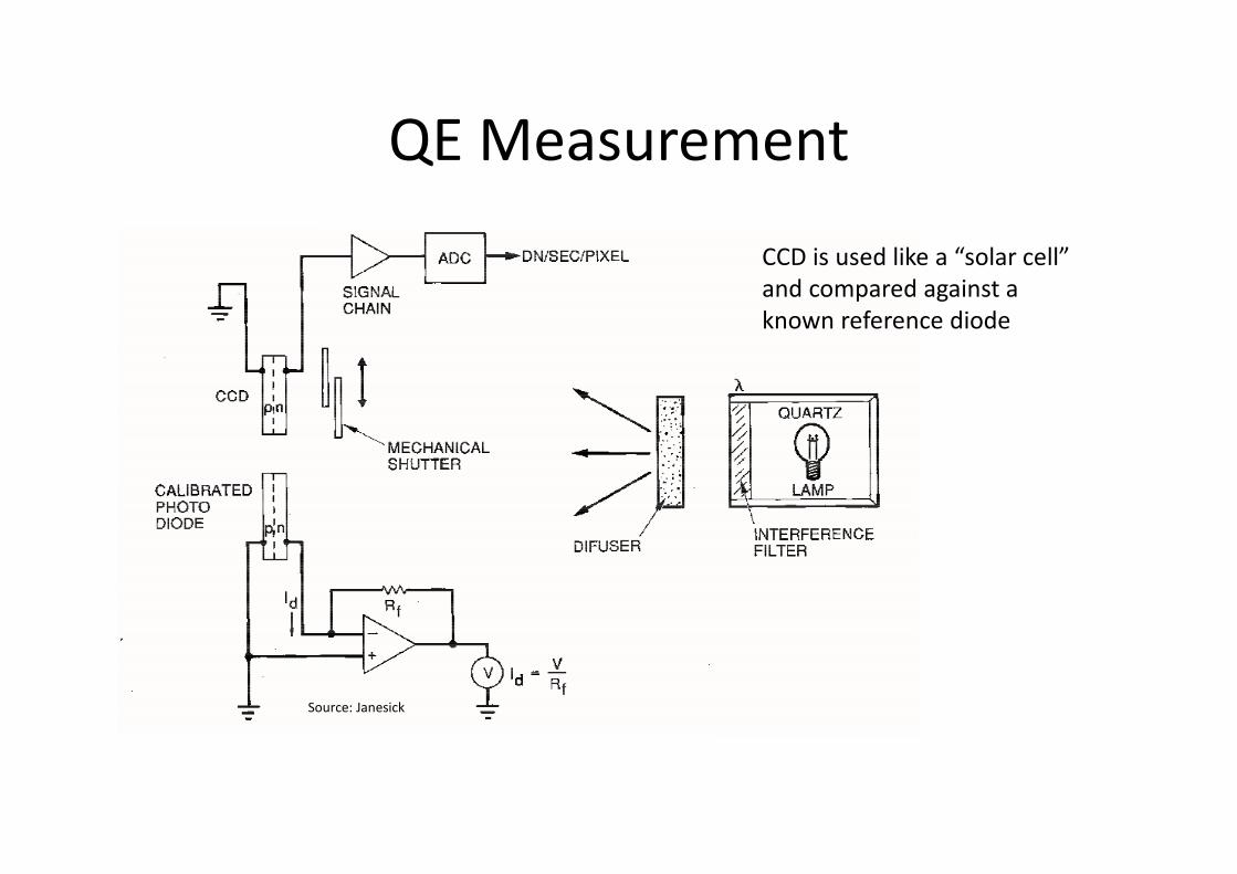
QE Measurement
CCD is used like a “solar cell”
and compared against a
known reference diode
Source: Janesick

QE doesn’t tell the whole story
• The entire CCD is used as a single light
collector for measuring QE
• If the photoelectrons are collected in the
wrong pixels, it makes no difference in the QE
value measured
• This can happen when NIR light is used for a
CCD

Diffusion MTF/Crosstalk
400nm light 900nm light
Longer wavelength light penetrates deeper before liberating photoelectrons / holes
If interaction happens outside potential well, then some charge will be captured by the wrong
pixel.
CCDs needed for NIR imaging need careful design / fab process optimization to have good
MTF.
Source: Janesick

MTF vs WavelengthVery poor
response for NIR
wavelengths
(>700nm)
At 400nm 65% of
charge ends up in
correct pixel at
Nyquist sampling
At 700nm only
40% does and at
900nm only 35%
does
NIR images taken
with this sensor
will have fine
detail smearedSource: Lomheim

Imaging at NIR wavelengths
• Kodak KAF series sensors have degraded MTF at NIR wavelengths
• Even with all-reflective optics (no chromatic aberration), poor sharpness results due to sensor Diffusion MTF/Crosstalk unless sensors *specifically* designed to work at NIR
• QE is only part of the story, MTF is the big issue for NIR
• Sensors designed for NIR imaging use specialized wafer fab processes and may include high substrate bias voltages to ensure good MTF (to prevent photoelectrons from forming outside of pixel potential wells)