properties and local environment of p-type … · aplicabilidade em sistemas electrónicos (p.ex....
TRANSCRIPT

CER
N-T
HES
IS-2
008-
192
13/1
0/20
08
UNIVERSIDADE DE LISBOA FACULDADE DE CIÊNCIAS
DEPARTAMENTO DE FÍSICA
PROPERTIES AND LOCAL ENVIRONMENT
OF P-TYPE DOPANTS AND PHOTOLUMINESCENT
RARE-EARTHS
IMPLANTED INTO ZNO SINGLE-CRYSTALS
Elisabete Maria Casa Nova Correia Rita
DOUTORAMENTO EM FÍSICA
2008


UNIVERSIDADE DE LISBOA FACULDADE DE CIÊNCIAS
DEPARTAMENTO DE FÍSICA
PROPERTIES AND LOCAL ENVIRONMENT
OF P-TYPE DOPANTS AND PHOTOLUMINESCENT
RARE-EARTHS
IMPLANTED INTO ZNO SINGLE-CRYSTALS
Elisabete Maria Casa Nova Correia Rita
Tese co-orientada pelo Dr. João Guilherme Correia e Dr. Ulrich Wahl
DOUTORAMENTO EM FÍSICA
2008


Summary
Keywords: ZnO, semiconductors, doping, p-type, rare-earth, implantation
This thesis presents an experimental study of the local environment of P-type and Rare-Earth dopants implanted in ZnO single-crystals (SCs). Various nuclear and bulk property techniques were combined in the following evaluations:
Implantation damage annealing
Implantation damage annealing was evaluated in ZnO SCs implanted with Fe, Sr and Ca.
P-type dopants
Cu and Ag implanted ZnO SCs were studied revealing that the solubility of Cu in substituting Zn is considerably higher than that of Ag. These results are discussed within the scope of the ZnO p-type doping problematic with these elements.
Experimental proofs of the As “anti-site” behavior in ZnO were for the first time attained, i.e., the majority of As atoms are substitutional at the Zn site (SZn), possibly surrounded by two Zn vacancies (VZn). This reinforces the theoretical prediction that As acts as an acceptor in ZnO via the AsZn-2VZn complex formation.
The co-doping of ZnO SC with In (donor) and As (acceptor) was addressed. The most striking result is the possible In-As “pair” formation. Two configurations are proposed for this “pair”, both with In and As at SZn. A purely In-related defect is also identified. These are preliminary experiments that can serve as guidelines for future and deeper studies.
Rare-earths (RE)
RE lattice site location, RE surface segregation and optical activation were investigated in Er and Tm implanted ZnO SCs, as a function of annealing temperature, implantation doses and implantation conditions. RE surface segregation and lattice recovery occur for high annealing temperatures, being more pronounced in the low dose implanted crystals. The RE-O clusters formation is suggested for the higher dose implanted samples.
Er and Tm optical activation occurs at different annealing temperatures depending on the implantation doses, suggesting that the RE-related emission is associated with defects/impurities in the RE close vicinity that change with the annealings.

Sumário Palavras-chave: ZnO, semicondutores, dopagem, tipo – p, terras – raras, implantação O estudo de semicondutores com grande hiato energético tem-se intensificado desde a
década de ’90 devido à sua aplicabilidade em sistemas fotónicos de curto comprimento de onda, bem como, em sistemas electrónicos de alta-frequência e alta potência. O interesse por este tipo de semicondutores começou com o GaN, mas rapidamente a comunidade científica se voltou para o semicondutor ZnO do tipo II-VI. Com um hiato energético de 3.437 eV (a 2K), o ZnO destaca-se pela elevada energia de ligação do excitão livre (60 meV), que o torna especialmente interessante para sistemas opto – electrónicos, bem como pela facilidade de crescimento de monocristais de alta qualidade. O ZnO apresenta ainda uma maior resistência à formação de defeitos induzidos por radiação e a recuperação da rede é também mais facilmente atingida.
Esta tese centra-se em dois dos principais tópicos de estudo da actualidade no âmbito do ZnO: a dopagem tipo–p e a dopagem com terras–raras (RE). Sendo intrinsecamente um semicondutor do tipo-n, a dopagem tipo-p do ZnO poderá potenciar ainda mais a sua aplicabilidade em sistemas electrónicos (p.ex. uma junção única pn). No entanto, esta tarefa tem-se revelado extremamente difícil, já que são muito poucos os casos de sucesso de dopagem eficiente tipo-p de ZnO. Quanto à dopagem com RE, é importante para a aplicação em sistemas fotónicos com emissão entre o visível e o UV.
As problemáticas associadas e estes dois tipos de dopantes, que serão enunciadas posteriormente, motivaram os estudos experimentais apresentados nesta dissertação. Mais concretamente, foram investigados os efeitos e o ambiente local destes dois tipos de dopantes em ZnO monocristalino. Os dopantes foram introduzidos por implantação iónica, uma técnica versátil e que permite um melhor controlo da dopagem, mas que ainda não foi suficientemente explorada para o caso do ZnO. Por este motivo, no estudo experimental aqui apresentado, começou-se por avaliar as condições ideais de recozimento térmico para recuperação da rede cristalina do ZnO após implantação. As implantações dos dopantes tiveram lugar em duas instituições diferentes, consoante a natureza do isótopo: no CERN/ISOLDE em Genebra (para isótopos radioactivos) e no ITN em Sacavém (para isótopos estáveis). Diferentes técnicas nucleares foram usadas nos estudos experimentais, nomeadamente, Canalização de Emissão de electrões (EC – Emission Channeling), Espectrometria de Retrodispersão de Rutherford (RBS) e Correlações Angulares Perturbadas (PAC). A luminescência das RE foi investigada por Fotoluminescência (PL - Photoluminescence). A combinação destas técnicas revelou-se extremamente importante na investigação dos seguintes temas:
iv Sumário
Recozimento dos defeitos de implantação Dado que os dopantes estudados na tese foram introduzidos no ZnO por implantação iónica, a primeira avaliação experimental consistiu na determinação das condições óptimas de recozimento dos defeitos da rede provocados pelas implantações. Este estudo foi efectuado em monocristais de ZnO implantados com isótopos de Fe, Sr e Ca, para diferentes temperaturas de recozimento e diferentes atmosferas (ar e vazio).
Dopantes tipo – p Foi investigado o comportamento dos dopantes Cu e Ag (grupo - Ib) implantados em monocristais de ZnO, revelando que a solubilidade do Cu para substituir os átomos de Zn (SZn) é consideravelmente superior à da Ag. É então proposto que o insucesso inerente à dopagem tipo-p de ZnO com Cu não deve ser atribuído à não-localização deste elemento no SZn. O mesmo não é verdade para a Ag, já que a baixa taxa de localização deste elemento no SZn deverá constituir a principal explicação para o fracasso nas tentativas de dopagem tipo-p com Ag. Como elemento do grupo – V, o As deveria actuar como aceitador no ZnO se localizado no sítio do O. No entanto, dada a elevada discrepância entre os raios iónicos do As e do O, esta explicação não era vista como aceitável para os poucos casos de sucesso de dopagem tipo-p de ZnO:As. Foi então previsto teoricamente, que o As seria mais estável no SZn (comportamento “anti-site”) e que deveria actuar como aceitador através da formação do complexo AsZn – 2VZn (VZn representa uma lacuna de Zn). Os resultados experimentais descritos na tese constituem precisamente, de forma inédita, a prova experimental há muito ambicionada do comportamento “anti-site” do As no ZnO. Mais precisamente, é demonstrado que a maioria dos átomos de As estão localizados no sítio SZn, não sendo afastada a hipótese de este elemento estar rodeado de duas VZn. O método da co-dopagem com um aceitador e um doador foi inicialmente proposto por teóricos como forma de ultrapassar as dificuldades inerentes à dopagem tipo-p do ZnO. A presença simultânea destes dois tipos de dopantes deverá reduzir a energia de Madelung da rede cristalina do ZnO, facilitando a incorporação e actuação do dopante aceitador. Todavia, este método não foi ainda investigado extensivamente, havendo por exemplo, muito pouca informação sobre o tipo de defeitos que se poderão formar e que poderão actuar de forma positiva ou negativa no processo de dopagem tipo-p. Mais ainda, existem poucas evidências experimentais sobre a localização dos dois tipos de dopantes coexistentes na rede do ZnO. No âmbito deste Doutoramento, a co – dopagem de ZnO monocristalino foi investigada com os dopantes In (doador) e As (aceitador). A possível formação de “pares” In-As após um tratamento térmico a 900ºC constitui o resultado mais importante deste estudo, já que poderá comprometer a eficiência da

Sumário v
dopagem tipo-p (através da passivação de carga). Com base nos resultados experimentais obtidos por PAC e EC, são propostas duas configurações para este “par” na rede cristalina do ZnO, ambas com In e As no sítio SZn. É ainda identificado um defeito relacionado puramente com o In, não sendo no entanto possível determinar a sua configuração exacta. É importante referir que estas experiências são preliminares já que mais medidas experimentais serão necessárias, bem como cálculos teóricos. No entanto, os resultados promissores que aqui são apresentados podem servir como linhas condutoras para estudos futuros mais aprofundados.
Terras – raras (RE) No âmbito da dopagem com terras-raras (RE), foram estudados monocristais de ZnO implantados com Er e Tm. A dopagem com estas RE é particularmente interessante para aplicações em sistemas opto–electrónicos com emissão no infra-vermelho. A emissão no visível destes elementos pode ainda ser utilizada em amplificadores ópticos e lasers. A principal problemática associada à dopagem de ZnO com terras-raras reside precisamente na técnica de dopagem. Regra geral as RE são introduzidas durante o crescimento do cristal resultando em amostras policristalinas e com formação de limites de grão de RE, que inibem a emissão óptica por parte destes elementos. A implantação iónica surge então como uma técnica promissora para a dopagem de ZnO com RE, não tendo, no entanto, até à data sido estudada de forma intensiva. A investigação experimental relacionada com RE, apresentada nesta tese, incidiu sobre a implantação e localização de Er e Tm na rede cristalina do ZnO (por EC), a avaliação da segregação destes elementos para a superfície (por RBS) e a detecção da sua activação óptica (por PL). Foi ainda avaliada a recuperação dos defeitos da rede provocados pelas implantações. Todos estes parâmetros foram estudados em função da temperatura de recozimento e das doses e condições de implantação. Os resultados revelam que a segregação de Er e Tm para a superfície e a recuperação da rede de ZnO ocorrem para temperaturas de recozimento elevadas, sendo estes efeitos mais pronunciados nos cristais implantados com menor dose de RE. É ainda sugerida a formação de clusters RE-O nos cristais implantados com maior dose, que inibem a recuperação da rede e a segregação da RE. A activação óptica do Er e do Tm ocorre para diferentes temperaturas de recozimento, dependendo da dose implantada. É então sugerido, que a emissão óptica associada a estas RE é fortemente influenciada pelos defeitos/impurezas existentes na sua vizinhança mais próxima, a qual sofre alterações com os tratamentos térmicos. Em determinadas condições experimentais, foram ainda identificadas algumas bandas ópticas associadas a defeitos intrínsecos do ZnO, nomeadamente, as bandas verde, vermelha e violeta.


Acknowledgements
This thesis is the result of a collaboration between the Centro de Física Nuclear da Universidade de Lisboa (CFNUL), the Instituto Tecnológico e Nuclear (ITN), the Universidade de Aveiro and the Organisation européenne pour la Recherche nucléaire (CERN/ISOLDE). I acknowledge the Fundação para a Ciência e Tecnologia for awarding me the scholarship for the completion of this Doctoral degree.
The present work represents for me the accomplishment of a long lasting goal which I
so often doubted I would ever achieve. For this, I am deeply grateful to a number of people, both at professional and personal level:
To, Professor Doutor José Carvalho Soares, I would like to thank in the first place
for giving me the opportunity to visit the “Lisbon group” at CERN when I finished my university graduation. This apparently simple visit changed my life and professional goals in a way that I never expected it to happen, and influenced me positively in going forward with the PhD work that is now resumed in this thesis. I am also infinitely grateful for the support, valuable advises and comprehension throughout these years, especially in the most delicate moments, and for taking the responsibility towards the university (CFNUL) and FCT, who awarded my Ph.D. scholarship.
To my PhD co-supervisors whom I would like to individually acknowledge. To Dr. João Guilherme Correia, who has also become a good friend, my sincere recognition for supporting my work in all aspects. Thank you for the constant energy, incentives and advises to do more and better. And above all thank you for always believing in me. To Dr. Ulrich Wahl, I am deeply grateful for transmitting me precious knowledge related with the EC technique, both at experimental and theoretical level, and for the permanent guidance through the EC experiments at CERN, even being 2000 Kms away. To all of you thank you for the understanding, enthusiasm and friendship.
To Dr. Eduardo Alves, I am indebted for supporting and orienting my work at ITN,
particularly in the rare-earth studies. To Dr. Teresa Monteiro, I am grateful for the PL measurements and for helping in
their interpretation. To the SSP group at CERN I am grateful for providing the four-detector PAC γ-γ
setup, especially to Dr. Marc Dietrich, Professor Wolfgang Tröger and Dr. Frank Heinrich for transmitting the know-how related with the PAC experiments, theory and data analysis.

viii Acknowledgements
To all the members of the ISOLDE collaboration, in particular to the in-house group, I am indebted for the expertise of working with radioactive isotopes and for helping with the experiments at CERN in so many different ways. Thank you for sharing the true meaning of CERN fellowship.
A special word to the members of the Lisbon group at CERN, who always received
me with open arms and supported the experiments. I am particularly indebted to my dear friend Armandina Lopes for the partnership in all the CERN experiments, for the good mood and above all for the long lasting friendship that made everything easier. To my good friend João Pedro Araújo, thank you for transmitting such enthusiasm for physics. To my friend Ana Cláudia Marques, I thank the company and the courage that she always demonstrated to all of us, to move on and never look back.
To the ITN technical group, in particular, Maria Filomena Baptista for helping in
setting on the accelerator every morning, and to Jorge Rocha for performing the stable isotopes implantations.
A special word to all the colleagues and friends of ITN for their support and
friendship ever since I joined ITN in 2001. In particular to my dear friend, Paula Cristina Chaves, for making of every working day, a good day to remember.
To all my friends at CERN, that made of my staying there a memorable period: Ana
Conde and Pedro Costa Pinto, Joana and Carlos, Ana Henriques, Suzana and Marco, Sandra, David, Leonel and Francisca, Paula and Rui, Serge Franchoo, Peter Cwetanski, Filip Moortgat, Enzo Carrone and many, many others.
Finally, I have no words to thank the pillars of my existence, the persons from whom I
receive the strength and willpower to proceed and that are always there for me: my whole family. In particular:
To my parents and sister, without them this thesis would never be made, without the sacrifices they did for so many years to provide me with this education, without the values they transmitted me, without their helping hand, support, strength and advises.
To my husband Bernardo, I am deeply thankful for his understanding since the early times of my PhD: the never-ending beam-times, the on-call experiments, the conferences, the so often bad moods. But also, I am grateful for staying by my side in every step that I take, for helping me to get up when I fell down and for pushing me forward until these final lines that I now write in the thesis.
And last but not least, I would like to thank a person that cannot yet read these lines. A person that turned my life upside down but that at the same time gave it a meaning. A person that in her own special way gave me strength to never give up and confidence in the future: my two years old daughter Beatriz.

Para a Beatriz
Para o Bernardo
À minha Família


Contents Introduction....................................................................................................................5 Synopsis............................................................................................................................9 1 Zinc Oxide – key features ..................................................................................11
1.1 ZnO lattice – main properties .......................................................................11 1.1.1 Crystallographic structure ................................................................12 1.1.2 Electrical properties..........................................................................14 1.1.3 Optical properties .............................................................................15
1.2 State-of-the-art..............................................................................................16 1.2.1 Ion implantation and damage annealing...........................................17 1.2.2 Ion implanted p-type dopants in ZnO...............................................17 1.2.3 Ion implanted rare-earths in ZnO .....................................................21
Bibliography ..........................................................................................................23
2 Experimental Techniques ..................................................................................27 2.1 Rutherford Backscattering Spectroscopy .....................................................27
2.1.1 General aspects .................................................................................28 2.1.2 Experimental setup ...........................................................................34 2.1.3 Data analysis.....................................................................................35
2.2 Photoluminescence .......................................................................................37 2.2.1 General aspects .................................................................................37 2.2.2 Experimental setup ...........................................................................39
2.3 Emission Channeling....................................................................................39 2.3.1 General aspects .................................................................................40 2.3.2 Classical theory of channeling for positive ions...............................41 2.3.3 Quantum theory of channeling- Electron emission channeling........44 2.3.4 Experimental setup ...........................................................................49 2.3.5 Data analysis.....................................................................................51
2.4 Perturbed Angular Correlations....................................................................53 2.4.1 General aspects .................................................................................53

2 Contents
2.4.1.1 Electric Quadrupole Interaction ........................................ 56 2.4.1.2 Magnetic Dipole Interaction.............................................. 58 2.4.1.3 Single-crystals features ..................................................... 59
2.4.2 Experimental setup........................................................................... 61 2.4.3 PAC experimental function and data analysis.................................. 63
Bibliography.......................................................................................................... 68
3 Samples Designation and Experimental Conditions ............................... 71 3.1 Implantation parameters............................................................................... 71 3.2 Annealing treatments.................................................................................... 75
4 Results and Discussion ....................................................................................... 77 4.1 Implantation damage annealing ................................................................... 77
4.1.1 57Fe implanted ZnO single-crystal ................................................... 78 4.1.2 89Sr and 45Ca as isoelectronic impurities.......................................... 80
4.2 Ion Implanted p-type dopants in ZnO SC .................................................... 84 4.2.1 Group Ib elements – Cu and Ag....................................................... 85
4.2.1.1 67Cu implanted in ZnO ...................................................... 85 4.2.1.2 111Ag implanted in ZnO..................................................... 88
4.2.2 Group V elements – As..................................................................... 96 4.2.3 Co-doping with In and As .............................................................. 100
4.2.3.1. – 111In in ZnO .................................................................... 101 4.2.3.2. – 111In and 73As co-doping ................................................ 109
4.3 Lattice location and Photoluminescent properties of RE implanted ZnO.. 125 4.3.1 Er implanted in ZnO....................................................................... 125
4.3.1.1 Er lattice site location...................................................... 125 4.3.1.2 Er diffusion and damage annealing................................. 127 4.3.1.3 Er optical activation ........................................................ 133
4.3.2 Tm implanted in ZnO..................................................................... 136 4.3.2.1 Tm lattice site location .................................................... 137 4.3.2.2 Tm diffusion and damage annealing ............................... 140 4.3.2.3 Tm optical activation....................................................... 153
4.3.3 Resume of the RE results ............................................................... 161 Bibliography........................................................................................................ 163
5 Final Conclusions and Perspectives............................................................. 167 Appendix A Nuclear decay schemes ................................................................ 173
A.1 89Sr → 89Y decay........................................................................................ 173 A.2 45Ca → 45Sc decay...................................................................................... 174 A.3 67Cu → 67Zn decay ..................................................................................... 174 A.4 111Ag → 111Cd decay .................................................................................. 174

Contents 3
A.5 73As → 73Ge decay .....................................................................................175 A.6 111In → 111Cd decay....................................................................................176 A.7 167Tm → 167mEr decay ................................................................................177 A.8 169Yb → 169Tm decay .................................................................................177

Chapter 1
Zinc Oxide – key features
This chapter intends to present the main features related with the II-VI semiconductor ZnO. The chapter starts with a description of ZnO’s lattice structure as well as its electrical and optical properties. It then continues with the state-of-the-art in p-type and rare-earth doping along with the associated problematic that motivated the studies described in this dissertation.
1.1. ZnO lattice – main properties ZnO is an II-VI wide bang-gap semiconductor (3.437 eV at 2K) with many
applications, such as piezoelectric transducers, varistors, phosphors and transparent conducting films. The range of applications was widespread in the last decade by the advances in production of large area single crystalline ZnO which made possible the fabrication of blue and UV light emitters, as well as, high-temperature high-power transistors. ZnO is also pointed out as a potential material for optoelectronic devices. However, this has been mainly limited by the difficulties in producing reproducible and low resistivity p-type doped ZnO, which is one of the problematic discussed in this thesis.
All the above referred ZnO-related applications are feasible and at the same time limited by its structural, electrical and optical properties, which are briefly described in what follows and resumed in Table 1.1 [53].

12 1.1 ZnO lattice – main properties
Table 1.1 – Properties of wurtzite ZnO
Lattice parameters at 300K a 0.324 95 nm c 0.520 69 nm
a / c 1.602 (1.633 in ideal hexagonal lattice) z 0.345 c
Density 5.606 g/cm3 Stable phase at 300K Wurtzite
Melting point 1975ºC Thermal conductivity 0.6, 1-1.2
Linear expansion coefficient (/C) a: 6.5×10⁻⁶ c: 3.0×10⁻⁶
Static dielectric constant 8.656 Refractive index 2.008, 2.029
Energy gap (at 2K) 3.437 eV, direct Intrinsic carrier concentration <106 cm-3
Exciton binding energy 60 meV Electron mobility at 300K for low n-type
conductivity 200 cm2/Vs
Hole mobility at 300K for low p-type conductivity
5-50 cm2/Vs
1.1.1. Crystallographic structure
The II-VI semiconductor ZnO crystallizes in the hexagonal wurtzite structure, in space group P63 mc, with lattice parameters c and a, ideally in the ratio c/a = 1.633 (Figure 1.1). It is composed by two interpenetrating hexagonal close-packed (hcp) sub-lattices, each of which consists of one type of atom (Zn or O) displaced with respect to each other along the three-fold c-axis by the amount of z = 0.375 c (in an ideal wurtzite structure). The z parameter is more simply defined as the Zn-O bond length along the c-axis in units of c. Each sub-lattice includes four atoms per unit cell and every atom of Zn is surrounded by four atoms of O, and vice-versa, which are coordinated at the edges of a tetrahedron. More precisely, the wurtzite structure consists of triangularly arranged alternating biatomic close-packed (0001) planes (Zn and O pairs in the case of ZnO). In this way, along the [0001] direction, the stacking sequence of the (0001) plane is AaBbAaBb..... The structure lacks inversion symmetry for which cutting the crystal perpendicular to the c-axis results in two structurally different surfaces with different polarities, i.e., terminated with one type of ions only (O or Zn face) (Figure 1.1).

1.1.1. Crystallographic structure 13
Figure 1.1 – Representation of the ZnO wurtzite lattice structure, with indication of the lattice constants a and c and of the z parameter (ZnO bond length along the c-axis). α and β are the bond angles with values of 109.47º in an ideal crystal. [1]
In a real ZnO crystal the mean lattice constants values are a = 3.250 Å and c = 5.206 Å,
but these depend slightly in stoichiometry variations, which result in deviations from the theoretical c/a ratio and the z parameter. Nevertheless, a strong correlation exists between them, i.e., when the c/a ratio decreases, the z parameter increases in such a way that the four tetrahedral distances remain nearly constant through a distortion of the tetrahedral angles related with long-range polar interactions. The two slightly different Zn-O bond lengths will be equal if the following relation holds [1],
z = 41
3 2
2
+ca (1.1)
The (0001) plane is the primary polar plane in wurtzite ZnO also called the basal plane. This plane and the associated [0001] direction are the most commonly used surface and direction for growth, though many other secondary planes and directions exist in the crystal structure. Figure 1.2 depicts the projections along the main symmetry crystallographic directions used in the experimental work described in this thesis ([0001], [1102], [1101] and [2113]).
a = 3.250 Å
c =
5.20
6 Å

14 1.1 ZnO lattice – main properties
Figure 1.2 – Projections along the main symmetry crystallographic directions of ZnO ([0001], [1102], [1101] and [2113]). These directions were used in the experiments presented in Chapter 4, particularly for the Emission Channelling technique.
Single crystalline ZnO is nowadays produced basically via three methods: Seeded
Chemical Vapour Transport (SCVT), hydrothermal and melt growth [1]. Though all of them yield high quality single crystals, the hydrothermal growth has revealed to be easier to control. More details about these growth methods can be found at Ref. [1] and the references therein. Important to refer that the ZnO single-crystals used in the work here presented were acquired from enterprises specialized in crystal growth (Eagle-Picher and Crystec).
1.1.2. Electrical properties
ZnO is attracting much attention for electronic and optoelectronic applications due to its direct and wide band-gap. The advantages of having a large band-gap include higher breakdown voltages, ability to sustain large electric fields, lower noise generation and high temperature high power operation.
Nominally undoped ZnO with a wurtzite structure is naturally an n-type semiconductor, that is, it has a high concentration of negative free charge carriers. These result from deviations of the stoichiometry due to the presence of intrinsic defects, such as,
ab
c
Zn
Along [0001]
ab
c
Zn O
Along [1101]
Along [1102]
ab
c
Zn O
Along [2113]
a
b
cZn
O

1.1.2. Electrical properties 15
the Zn on O antisite, the Zn interstitial (ZnI) and the O vacancy (VO) [2]. Theoretical calculations suggest that hydrogen occurs only in the positive form inside ZnO, being thus also pointed out as responsible for the intrinsic n-type behaviour of ZnO [3]. This assumption is valid since hydrogen is always present in all growth methods and can easily diffuse into ZnO in large amounts due to its large mobility. Undoped ZnO shows intrinsic n-type conductivity with high electron densities around 106 cm-3 [4]. By means of Monte Carlo simulations, Albrecht et al. [5] predicted the room temperature electron mobility in ideal ZnO as ~300 cm2/Vs. However, lower values have been attained in real ZnO (200 cm2/Vs), depending also on the growth method.
The density of charges carriers can be increased in semiconductors by doping with an appropriate element. While n-type doping of ZnO is nowadays relatively easy to achieve, the same is not true for p-type (positive free charge carriers, i.e., holes). As referred previously, it is highly desirable the achievement of p-type ZnO since in this way the potentialities of this II-VI semiconductor would be fully employed in optoelectronic devices. Many causes have been pointed out for the inherent difficulty in achieving high concentration of holes with high mobility in ZnO, namely, compensation of dopants by low-energy native defects (Zni or VO) or background impurities (H, for instance), low solubility of the dopant in ZnO and deep impurity level resulting in a significant resistance to the formation of a shallow acceptor level [1 and reference therein]. The p-type doping of ZnO is one of the main topics studied in the scope of this PhD and it is described with higher detail in section 1.2.
1.1.3. Optical properties
ZnO has a potential application in blue and ultraviolet (UV) light emitters as well as UV detectors operating at high temperatures [6]. It presents a significant excitonic emission at room temperature due to its large free-exciton binding energy of 60 meV. Moreover, many sharp near band-edge transition lines are frequently observed in the absorption and luminescence spectra of high quality ZnO single-crystals acquired at low temperatures.
The optical properties of a semiconductor are related with both intrinsic and extrinsic effects. More precisely, intrinsic optical transitions take place between the electrons in the conduction band and the holes in the valence band, including excitonic effects due to Coulomb interaction. An exciton is a bound state of an electron and a hole, like an “electron-hole pair”. It results from the Coulomb binding of an electron that was excited into the conduction band with its hole. The exciton has thus slightly less energy than the unbound electron and hole and it has an overall charge of zero. Excitons are the main mechanism for light emission in semiconductors at low temperatures. They are classified into free and bound excitons and, in some cases, the free exciton can also exhibit excited states. These states may be inferred from the light absorption associated with their excitation.

16 1.2 State-of-the-art
The extrinsic optical transitions are related with dopants or defects that form discrete electronic states within the band-gap, influencing thus the optical absorption and emission spectra. In the presence of dopants, excitons could, in theory, bound to neutral or charged donors or acceptors forming bound excitons (BE). The BE electronic states are strongly dependent on the semiconductor band structure. Two of the most important bound excitons cases are the DBE (shallow neutral donor bound exciton) and the ABE (shallow neutral acceptor bound exciton).
Optical transitions in ZnO have been studied by a variety of experimental techniques, namely, optical absorption, transmission, reflection, photoreflection, spectroscopy ellipsometry, photoluminescence, cathodoluminescence, calorimetric spectroscopy, etc. All these techniques lead to a better understanding of the intrinsic and extrinsic transitions in ZnO. Besides the intrinsic excitonic properties and the donor and acceptor bound excitons above referred, other recombination phenomena can be observed. For instance, a two-electron satellite (TES) transition, resulting from the neutral-donor-bound exciton transition, which is typically observed in ZnO in the 3.32-3.34 eV spectral region. Also, LO-phonon replicas of the main excitonic emissions can be observed. Though this spectral region has not yet been extensively studied in ZnO, it is known that LO-Phonon replicas occur with a separation of 71-73 meV, the LO-Phonon energy in ZnO.
Up do date there are not many point defect studies in ZnO. Nevertheless, it is common to observe defect-related transitions in the optical spectra, such as, free-to-bound (electron-acceptor), bound-to-bound (donor-acceptor) and the so-called green, yellow and red luminescence bands [1]. Some authors suggest that the broad green luminescence band (peak at ~2.5 eV) commonly observed in undoped n-type ZnO is due to the presence of intrinsic Zn vacancies (VZn) [7]. For others, the presence of Cu at the Zn site can be also the reason for the green band [8]. A yellow band peaking at 2.2 eV and with a FWHM of ~0.5 eV was observed following Li doping [9]. A red luminescence band at 1.75 eV was seen at 1.75 eV after a 700ºC air annealing [1]. There is also some information available regarding the shallow donor-acceptor-pair (DAP) band with a sharp peak at 3.22 eV and followed by at least two LO-Phonon replicas. This emission has been attributed to the DAP transitions involving a shallow donor and a shallow acceptor [10].
Several dopant-related luminescent transitions are known in ZnO [1]. There is a particular interest in Rare Earth doping envisaging optoelectronic applications with emission from visible to UV. These are discussed in detail in section 1.2.
Further and more detailed information regarding the optical properties of ZnO can be found at Ref. [1] and references therein.
1.2. State-of-the-art
In this section the state-of-the-art of ZnO is reviewed, with particular emphasis to the main issues studied in the present work, namely, the p-type doping and rare-earth doping

1.2.1. Ion implantation and damage annealing 17
of ZnO. A description of the advances made in these areas is firstly presented, followed by the key questions that motivated the studies presented in Chapter 4. The section will start with a brief reference to ion implantation, as this was the selected doping technique for the studies presented in this dissertation.
1.2.1. Ion implantation and damage annealing
Since long that ZnO is commonly doped during growth, for instance, via wet-chemical synthesis, sintering and laser ablation. In spite of successful results, in some cases these doping techniques impose limits in the doping effects. For instance, introduction of rare-earths (RE) in ZnO during growth has often resulted in RE accumulation at grain boundaries [11], which poses a problem in terms of their luminescence.
Ion implantation arises thus as an attractive doping technique of the highly resistant ZnO single-crystals. It presents significant advantages, namely, easier control of the depth, dose and lateral patterning of the dopant, the possibility of introducing different dopants at different depths and the fact that it is a cheaper and more versatile technique, currently used in Si technology.
Doping by ion implantation is particularly interesting in the case of ZnO as it reveals to be highly resistant to ion-beam-damage formation, even after implantation of keV heavy ions at high doses (~1017 at/cm2) [12-14]. Indeed, ZnO proved to be more resistant to ion implantation than the well known GaN. The effects induced by the dopant are intimately related with the doping technique itself, as it plays an important role in the formation of lattice defects, as well as, on the dopant lattice site location. These are the main factors that influence and/or degrade the effects of semiconductors doping, for which their evaluation is crucial. This brings us to another advantage of using ion implantation with ZnO since the implantation damage can be largely removed through thermal annealing [14].
It becomes clear that the evaluation of the optimum annealing conditions and the lattice and dopants behaviour as a function of these annealings is peremptory. This study was, therefore, firstly performed and is presented in section 4.1 following the implantation of stable Fe and the radioactive isotopes 89Sr and 45Ca. These are isoelectronic elements to Zn and can thus provide valuable information regarding the lattice recovery. The studies were carried out by means of Rutherford Backscattering Spectrometry (RBS) and Emission Channelling (EC) techniques.
1.2.2. Ion implanted p-type dopants in ZnO
It is well known that in all wide-band-gap semiconductors only one type of doping (n- or p- type) is easily achieved. According to some authors [15, 16], the origin for the doping difficulties lays in the spontaneous creation of amphoteric defects that will impose limits in the range of available positions of the Fermi level in thermal equilibrium. Other hypotheses

18 1.2 State-of-the-art
suggest the presence of compensating native defects [2] (Zn interstitials and O vacancies) and/or the non-incorporation of the dopant at a proper lattice site to act as an acceptor [17]. Moreover, a structural defect known as AX centre is commonly formed when doping with acceptors. This is a deep defect complex that compensates for acceptors [17] and in binary semiconductors it forms through a double broken bond (DBB) mechanism [18] which results in the release of two electrons (equivalent to the capture of two holes).
For the particular case of the intrinsically n-type doped ZnO, finding a suitable acceptor is not at all an easy task. The most attractive p-type dopants for this II-VI semiconductor are the group-I and group-V elements, which could act as acceptors if incorporated in substitutional Zn sites (for group-I dopants) or in substitutional O sites (for group-V dopants). However, to date, successful p-type doping has been reported only for group–V elements N and P [19] and also As [20-25] and Sb [26], but the mechanism through which these elements act as simple acceptors on O sites is not well understood.
Theoretical predictions suggest that the p-type doping efficiency for both group-I and group-V elements is limited by the formation of self-compensation dopant-related mechanisms. More precisely, the formation of group-I dopants interstitials is quite stable, particularly for Li and Na, and these will act as donors instead of acceptors [17]. In contrast, group-V dopants tend to occupy anti-sites that would act as charge compensators [17]. Indeed, according to theoretical calculations these group-V dopants should be more stable at Zn sites [17, 27] also because of the considerable ionic radii mismatch of these elements with O [19]. Moreover, in contrast to group-I elements, the above referred AX centres are believed to be quite stable for group-V impurities, especially for P and As [17]. Therefore, for the particular case of group-V dopants, the mechanism behind the observed p-type doping is not clear. The few successful cases of p-type doped ZnO together with the little understanding of the mechanisms behind it lead theoreticians to propose new methodologies. The most popular is the co-doping method, pointed out as an efficient p-type doping process for II-VI semiconductors [28-31].
In what follows, these issues will be discussed in detail within the scope of the p-type dopants studied in the PhD work here presented.
Group-Ib elements – Cu and Ag In this work Cu and Ag were selected as interesting group-Ib elements to study within the scope of ion implantation of p-type dopants.
Cu is believed to act as an acceptor in ZnO if incorporated at substitutional Zn sites, with possible applications on varistors [32] and piezoelectric devices [33]. Furthermore, the acceptor behaviour of Cu in ZnO apparently explains its successful role as a co-dopant in the activation of room-temperature ferromagnetism in Zn0.94Fe0.05Cu0.01O [34].
Besides the influence on the electrical properties, the 3d transition metal Cu is a common impurity in as-grown ZnO crystals [8, 35-37] and has since long been considered

1.2.2. Ion implanted p-type dopants in ZnO 19
as the main responsible for the “structured” green luminescence [8, 35-38] characteristic of this II-VI semiconductor. More precisely, the origin of this luminescence has been attributed to Cu located at substitutional Zn sites [8], but other theories suggest that the green band is related with the intrinsic presence of Zn [7] or O vacancies [39]. At the time that the experimental work of this PhD was performed, none of the above mentioned models had been unquestionably selected. This occurred only recently following Photoluminescence (PL) studies with radioactive isotopes, performed at CERN/ISOLDE, which attributed the “structured” green band to the intrinsic presence of Zn vacancies (VZn) [40].
Electron Paramagnetic experiments have given an indirect evidence for substitutional Cu2+ at Zn sites [41, 42], while infrared luminescence suggests the presence of several different Cu defects [35, 38]. Resistivity measurements point towards the passivation of CuZn acceptors by O vacancies [43, 44] or the formation of acceptor-type Cu2+ - Cu2+ pairs [42]. However, the fact is that so far there are no reported experiments that studied in detail the structural properties of this p-type dopant in ZnO.
In what concerns Ag, it is one of the potential acceptors in ZnO if incorporated on substitutional defect-free Zn (SZn) sites. Nevertheless, previous studies, where Ag-doped ZnO was investigated with respect to its application in varistors, suggested that this element acts as an amphoteric dopant, existing both on substitutional Zn sites and in the interstitial form [15]. If this scenario is real, it would then be extremely difficult to attain p-type doped ZnO with Ag.
In both cases it becomes clear the relevance of identifying the lattice site location of Cu and Ag in ZnO. Since Cu has an atomic mass smaller than Zn it is difficult to determine the lattice site location of this dopant by means of Rutherford Backscattering Spectroscopy (RBS) and Ion Beam Channelling techniques. Using these techniques together with Particle Induced X-ray Emission (PIXE) would allow the determination of the Cu lattice site, but this is also very complicated in this case, since the X-ray emission lines of Cu are very similar to the ones of Zn. The same is not true for Ag, since it is heavier then Zn. Emission Channelling (EC) arises, particularly for Cu, as a privileged technique to identify the lattice site location of Cu in ZnO. Though for the case of Ag it would be possible to perform RBS/Channelling experiments, EC was also selected as a more adequate technique for precise lattice site location evaluation, as it is more sensitive, in particular, for relatively low dopant concentrations. The results from these studies are presented and discussed in section 4.2.1. Group-V elements – As In what concerns the group-V dopants, As was selected to study since successful cases of As p-type doped ZnO can be found already in the literature [20-25]. The main problematic associated with As is the explanation of the mechanism behind the p-type behaviour of ZnO, i.e., how does As act as an acceptor in ZnO. To act as an acceptor As would have to be substitutional at O sites. However, theoretical predictions

20 1.2 State-of-the-art
suggest that As prefers an “anti-site” behaviour. That is, As would be more stable at Zn sites rather than O and, if substituting O, the energy levels of As would be located deep in the ZnO band-gap [17, 27]. Moreover, due to the large mismatch between the ionic radii of As3- (2.22 Å) and O2- (1.38 Å) it was argued that As should have a low solubility substituting for O in ZnO [19]. A model was then proposed to explain the p-type character of ZnO following As doping. According to the authors in Ref. [27] the acceptor action is due to AsZn – 2VZn complexes, where an As atom occupies a Zn “anti-site” and is surrounded by two Zn vacancies.
From what was here described, it is clear that there exist several strong arguments against the hypothesis of the p-type doping behaviour of ZnO, following As doping, being mainly related to the location of this dopant at oxygen sites. However, until now, no experimental method was able to provide reliable knowledge on the lattice site of As in ZnO, which motivated the experiments described in section 4.2.2. Following ion-implantation, the dopant lattice site location was evaluated as a function of annealing temperature by means of Emission Channelling (EC). Co-doping with In and As Though p-type doped ZnO was already produced by incorporation of As alone [23], the deep acceptor levels, the low solubility of the dopant and the formation of AX centres (structural defect explained in above) result in low carrier concentrations, making acceptor doping of ZnO very difficult. The same is true for other group-V p-type dopants (N and P). Several attempts have been made to try to solve this problem, but with no significant success. More recently, theoreticians have proposed that the simultaneous doping of ZnO with an acceptor and a donor in the ratio acceptor:donor ≈ 2:1 would lead to efficient p-type doping. This is the so called co-doping method [28-31].
Theoretical results suggest that the presence of the donor will positively influence the incorporation and stability of the acceptor in the proper lattice site by decreasing the Madelung lattice energy [28-31]. Several donor-acceptor pairs were suggested by theory based on the most promising p-type dopants As and N. For the particular case of As, theoretical calculations suggested that co-doping with the donor Ga would reduce the Madelung energy of the lattice and thus increase the solubility and stability of As in ZnO [30]. One of the reported synthesis of p-type doped ZnO with As was accomplished by deposition of ZnO films on (001)-GaAs [20]. Secondary ion mass spectroscopy (SIMS) has shown that both Ga and As had diffused into ZnO during post annealing suggesting that Ga played an important role in the p-type doping process. A similar scenario is true for the ZnO doping with N, but this time with the donor In. Several authors reported the successful production of ZnO films co-doped with In and N and some of them with high hole mobility [45, 29].
In spite of the successful cases reported above there are still questions to be addressed concerning this co-doping method. The dopant lattice site location is essential to fully

1.2.3. Ion implanted rare-earths in ZnO 21
understand this doping mechanism. Also, there is little experimental information about the presence and nature of the defects that could influence in a positive or negative way the p-type doping. One of them is for instance the formation of donor-acceptor “pairs”. This “pair” formation should be interpreted more as a “close interaction” rather than a real donor-acceptor bond formation, though this hypothesis should not be completely excluded depending on the dopants nature. In this case, charge passivation would take place and the p-type doping would not be achieved. Moreover, the use of ion implantation for co-doping of ZnO is not well studied.
Though the Ga-As and In-N co-doping pairs have been firstly proposed by theory, the In-As pairing has been chosen to study in this PhD due to the fact that these samples are easier to prepare by ion implantation. Also, a considerable amount of work had been done already within the scope of this PhD with the individual implantations of In and As in un-doped ZnO. The motivations for the individual study of As in ZnO were already presented above. In what concerns the individual study of In in ZnO, it is important given the promising application of this dopant in the production of transparent conducting oxides (TCO), which can be used for optoelectronic devices, such as, solar cells [46], liquid crystal displays [47] and heat mirrors [48].
In the work here presented the author proposes to address the In-As co-doping problematic by means of the EC and PAC techniques which can provide the necessary information about the dopants lattice site, their local environment and the possible formation of the charge compensating In-As “pair” (section 4.2.3). Nevertheless, it is important to stress that this is a preliminary study, as it arose at a later stage of the PhD. 1.2.3. Ion implanted rare-earths in ZnO
Rare-earth (RE) doped semiconductors are since long being investigated due to their potential application as optoelectronic emission devices from visible to UV [49]. ZnO is not an exception, particularly after being experimentally proved that rare-earth luminescent efficiency at room temperature (RT) increases with the semiconductor band-gap [50]. Following successful results with rare-earth doped GaN, the solid state physics community turned their attention to ZnO, as it is similar to GaN, but with the advantages of high-quality single-crystals being much easier to grow and of higher resistance to doping defect formation.
Several methods have been used for RE doping of ZnO, such as sintering, wet-chemical synthesis and laser ablation. However, these methods result in polycrystalline samples with RE accumulation at grain boundaries [11]. This poses a problem, as the RE luminescence in semiconductors has since long been attributed to their location at substitutional Ga (for GaN) or Zn (for ZnO) sites. In this sense, ion implantation arises as an attractive doping technique for ZnO single-crystals taking into account that they are

22 1.2 State-of-the-art
highly resistant to the formation of implantation damage. This technique has not yet been extensively studied for the particular case of RE doping of these crystals.
In this thesis the ion implantation of Er and Tm in ZnO was evaluated whose results are presented in section 4.3. These RE are particularly interesting for infrared emitting optoelectronic devices, for optical fibre telecommunication systems, due to their intra-4f shell transitions in the 1.4-1.7 µm range. Moreover, with visible emission from higher excited levels (green for Er and blue for Tm) they can potentially be used in devices such as optical amplifiers, lasers and optically pumped glass fibres [49, 51].
The development of this kind of devices is crucial for the advance of short-range high-speed networks operating in the infrared. As for Tm, it is known to be a potential dopant for blue emission [52]. In both cases, there is an urge for improvement of these RE applications in the visible spectral region. For this, it is important to understand the RE ions fundamental properties in wide band gap semiconductors, such as its lattice site location and surroundings and the optical ion activation mechanisms and emission properties.

Bibliography
[1] – Ű. Őzgür, Ya. I. Alivov, C. Liu, A. Teke, M. Reshchikov, S. Doğan, V. Avrutin, S.
– J. Cho and H. Morkoç, J. Appl. Phys. 98, 041301 (2005) [2] – D.C. Look, J.W. Hemsky and J.R. Sizelove, Phys. Rev. Lett. 82, 2552 (1999)
[3] – C. G. Van de Walle, Phys. Rev. Lett. 85, 1012 (2000)
[4] – T. Minami, H. Sato, H. Nanto, and S. Takata, Jpn. J. Appl. Phys. 24, L781 (1985)
[5] – J. D. Albrecht, P. P. Ruden, S. Limpijumnong, W. R. L. Lambrecht, and K. F.
Brennan, J. Appl. Phys. 86, 6864 (1999)
[6] – D. C. Look, Mat. Sci. Eng. B 80, 381 (2001)
[7] – A.F. Kohan, G. Ceder, D. Morgan and C.G. Van de Walle, Phys. Rev. B 61, 15019 (2000)
[8] – R. Dingle, Phys. Rev. Lett. 23, 579 (1969)
[9] – O. F. Schirmer and D. Zwingel, Solid State Commun. 8, 1559 (1970)
[10] – K. Thonke, T. Gruber, N. Trofilov, R. Schönfelder, A. Waag and R. Sauer,
Physica B 308, 945 (2001)
[11] – S. Bachir, K. Azuma, J. Kossanyi, P. Valat, and J.C. Ronfard-Haret, J. Lumin. 75, 35 (1997)
[12] – H.M. Naguib and R. Kelly, Radiat. Eff. 25, 1 (1975)
[13] – C. W. White, L. A. Boatner, P. S. Sklad, C. J. McHargue, S. J. Pennycook, M. J.
Aziz, G. C. Farlow and J. Rankin, Mater. Res. Soc. Symp. Proc. 74, 357 (1987)
[14] – E. Sonder, R. A. Zuhr and R. E. Valiga, J. Appl. Phys. 64, 1140 (1988)
[15] – J. Fan and R. Freer, J. Appl. Phys. 77(9), 4795 (1995)
[16] – W. Walukiewicz, Physica B 302, 123 (2001)

24 Bibliography
[17] – C.H. Park, S.B. Zhang and Su-Huai Wei, Phys. Rev. B 66, 073202 (2002)
[18] – C.H. Park and D. J. Chadi, Phys. Rev. Lett. 75, 1134 (1995)
[19] – S. J. Pearton, D. P. Norton, K. Ip, Y.W. Heo and T. Steiner, J. Vac. Sci. Technol. B 22, 932 (2004)
[20] – Y. R. Ryu, S. Zhu, D. C. Look, J. M. Wrobel, H. M. Jeong and H.W. White, J.
Cryst. Growth 216, 330 (2000)
[21] – Y. R. Ryu, T. S. Lee and H.W. White, Appl. Phys. Lett. 83, 87 (2003)
[22] – Y. R. Ryu, T. S. Lee, J. H. Leem and H.W. White, Appl. Phys. Lett. 83, 4032 (2003)
[23] – D. C. Look, G. M. Renlund, R. H. Burgener II and J. R. Sizelove, Appl. Phys. Lett.
85, 5269 (2004)
[24] – W. Lee, M. Jeong and J. Myoung, Appl. Phys. Lett. 85, 6167 (2004)
[25] – V. Vaithianathan, B. Lee and S. S. Kim, Appl. Phys. Lett. 86, 062101 (2005)
[26] – T. Aoki, Y. Shimizu, A. Miyake, A. Nakamura, Y. Nakanishi and Y. Hatanaka, Phys. Status Solidi B 229, 911 (2002)
[27] – S. Limpijumnong, S. B. Zhang, S. H. Wei and C. H. Park, Phys. Rev. Lett. 92,
155504 (2004)
[28] – S. B. Zhang, J. Phys. Condens. Matter 14, R881 (2002)
[29] – T. Yamamoto and H.K. Yoshida, Jpn. J. Appl. Phys. 38, L166 (1999)
[30] – T. Yamamoto and H.K. Yoshida, Physica B 302-3038, 155-162 (2001)
[31] – T. Yamamoto, Phys. Status Solidi A 193, 423-433 (2002)
[32] – T.R.N. Kutty and N. Raghu, Appl. Phys. Lett. 54, 1796 (1989)
[33] – J.B. Lee, H.J. Lee, S.H. Seo and J.S. Park, Thin Solid Films 398, 641 (2001)
[34] – S.J. Han, J.W. Song, C.H. Yang, S.H. Park, J.H. Park, Y.H. Yeong and K.W. Rhie, Appl. Phys. Lett. 81, 4212 (2002)
[35] – H.J. Schulz and M. Thiede, Phys. Rev. B 35, 18 (1987)
[36] – P. Dahan, V. Fleurov, P. Thurian, R. Heitz, A. Hoffmann and I. Broser, J. Phys.:
Condens. Matter 10, 2007 (1998)
[37] – N.Y. Garces, L. Wang, L. Bai, N.C. Giles, L.E. Halliburton and G. Cantwell, Appl. Phys. Lett. 81, 622 (2002)

Bibliography 25
[38] – P.J. Dean, D.J. Robbins, S.G. Bishop, J.A. Savage and P. Porteous, J. Phys. C 14, 2847 (1981)
[39] – S.B. Zhang, S.H. Wei and A. Zunger, Phys. Rev. B 63, 075205 (2001)
[40] – M. Deicher and The ISOLDE Collaboration, Physica B 389, 51-57 (2007)
[41] – R.E. Dietz, H. Kamimura, M.D. Sturge and A. Yariv, Phys. Rev. 132, 1559 (1963) [42] – G. Müller and R. Helbig, J. Phys. Chem. Solids 32, 1971 (1971)
[43] – G. Bogner and E. Mollwo, J. Phys. Chem. Solids 6, 136 (1957)
[44] – G. Bogner, J. Phys. Chem. Solids 19, 235(1961)
[45] – J. M. Bian, X. M. Li, X. D. Gao, W. D. Yu, and L. D. Chen, Appl. Phys. Lett. 84,
541 (2004)
[46] – S. Major and K.L. Chopra. Sol. Energy Mater. 17, 319 (1988)
[47] – J. Lan and J. Kanicki, Mater. Res. Soc. Symp. 424, 347 (1997)
[48] – K. L. Chopra, S. Major and D. K. Panday, Thin Solid Films 102, 1 (1983)
[49] – T. Gregorkiewicz and J. M. Langer, Mater. Res. Bull. 24, 27 (1999)
[50] – P.N. Favennec, H. L’Haridon, D. Moutonnet, M. Salvi and M. Gaunneau, Mater. Res. Soc. Symp. Proc. 301, 181 (1993)
[51] – A. Polman, J. Appl. Phys. 82, 1 (1997)
[52] – T. Monteiro, J. Soares, M.R. Correia, E. Alves, J. Appl. Phys. 89, 6183 (2001)
[53] – D. W. Palmer, http://www.semiconductors.co.uk, 2002.06


Chapter 2
Experimental Techniques
Several key issues related with ZnO doping via ion implantation were investigated in this PhD work, such as, the lattice damage induced by the implanted species and the lattice recovery with subsequent annealing treatments. Furthermore, the optical activation of luminescent dopants (rare-earths), the local environment in the dopant neighborhood and the dopant lattice site location were also addressed. All these subjects will lead us in the complex way of understanding the dopant behavior and the doping processes consequences in ZnO single-crystals. These features were evaluated by means of complementary experimental techniques, whose combination of results allowed an enhanced insight into ion implanted ZnO single-crystals.
The ZnO sample’s crystalline quality, as well as, the implanted dopants diffusion and lattice defect recovery were evaluated using the Rutherford Backscattering/Channeling technique (RBS/C). With Photoluminescence (PL), the optical activation of the dopant was addressed. The lattice site location of the dopant and its local environment inside the ZnO lattice were studied by means of Emission Channeling (EC) and Perturbed Angular Correlations (PAC), respectively.
Given the extensive number of publications available among the scientific community with a thoughtful explanation of the above referred techniques, in what follows only their main experimental and theoretical features are presented.
2.1. Rutherford Backscattering Spectroscopy
Rutherford Backscattering Spectroscopy/Channeling (RBS/C) is a non-destructive technique based on the elastic collision of an incident particle with a target nucleus, during which an energy transfer occurs, from the particle to the nucleus. The amount of energy transferred depends on the nature of the target nucleus. Therefore, by measuring the energy of the dispersed particle the identity of the target nucleus can be known. Moreover, the final energy of the dispersed particle is also an indication of the depth at which the

28 2.1. Rutherford Backscattering Spectroscopy
collision took place. This means that a depth profile of the analyzed sample can be determined. Further information can be extracted from the RBS/C spectra, such as, surface composition, concentration profiles and film thickness. All these factors make of this technique a powerful tool in the field of materials characterization.
2.1.1. General aspects
Figure 2.1 (a) illustrates the above referred basic principles for a composed sample AmBn where A is heavier than B.
Figure 2.1 – Dispersion geometry and resulting experimental spectrum for a composed sample AmBn.
In this example, an incident particle with initial energy E0 looses energy and is dispersed by interacting with the atoms of the sample. This interaction can occur immediately at the surface or at a given depth t. In the simplest case of surface interaction, the particle is scattered by an angle θ = 180º-θ1-θ2 and will have a final energy of KAE0 or KBE0 depending on whether it collided with atom A or atom B, respectively. KA (or KB) represents the kinematic factor, given by the quotient between the final energy of the particle and its initial energy in an interaction with atom A (or B). It characterizes, therefore, the energy lost on the collision. By making use of the laws of energy and linear momentum conservation the kinematic factor depends only on the masses of the incident particle and of the target nucleus, as well as on the dispersion angle. For the case of a collision with atom A we get [1],
KA =
2
Ap
22p
2Ap
0
f
MM
θsinMMcosθM
E)(E
⎟⎟⎟
⎠
⎞
⎜⎜⎜
⎝
⎛
+
−+=
A (2.1)
E0
θ1
KAE0 KBE0
θ2
KAE KBE
θ
tE
Ef (A) = KAE0 - ΔEA Ef (B) = KBE0 - ΔEB
Yield
Energy KBE0 KAE0
A
B
HA,0 HB,0
HB
θ
Ef (A) Ef (B)
ΔE (B)
ΔE (A) Detector
a) b)
2.1.1 General aspects 29
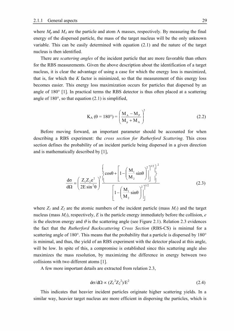
where Mp and MA are the particle and atom A masses, respectively. By measuring the final energy of the dispersed particle, the mass of the target nucleus will be the only unknown variable. This can be easily determined with equation (2.1) and the nature of the target nucleus is then identified.
There are scattering angles of the incident particle that are more favorable than others for the RBS measurements. Given the above description about the identification of a target nucleus, it is clear the advantage of using a case for which the energy loss is maximized, that is, for which the K factor is minimized, so that the measurement of this energy loss becomes easier. This energy loss maximization occurs for particles that dispersed by an angle of 180° [1]. In practical terms the RBS detector is thus often placed at a scattering angle of 180°, so that equation (2.1) is simplified,
KA (θ = 180°) = 2
Ap
PA
MMMM
⎟⎟⎠
⎞⎜⎜⎝
⎛
+− (2.2)
Before moving forward, an important parameter should be accounted for when describing a RBS experiment: the cross section for Rutherford Scattering. This cross section defines the probability of an incident particle being dispersed in a given direction and is mathematically described by [1],
1/22
2
1
21/22
2
1
2
2
221
sinθMM1
sinθMM
1cosθ
θsin 2EeZZ
dΩdσ
⎥⎥⎦
⎤
⎢⎢⎣
⎡⎟⎟⎠
⎞⎜⎜⎝
⎛−
⎪⎭
⎪⎬⎫
⎪⎩
⎪⎨⎧
⎥⎥⎦
⎤
⎢⎢⎣
⎡⎟⎟⎠
⎞⎜⎜⎝
⎛−+
⎟⎟⎠
⎞⎜⎜⎝
⎛= (2.3)
where Z1 and Z2 are the atomic numbers of the incident particle (mass M1) and the target nucleus (mass M2), respectively, E is the particle energy immediately before the collision, e is the electron energy and θ is the scattering angle (see Figure 2.1). Relation 2.3 evidences the fact that the Rutherford Backscattering Cross Section (RBS-CS) is minimal for a scattering angle of 180°. This means that the probability that a particle is dispersed by 180° is minimal, and thus, the yield of an RBS experiment with the detector placed at this angle, will be low. In spite of this, a compromise is established since this scattering angle also maximizes the mass resolution, by maximizing the difference in energy between two collisions with two different atoms [1].
A few more important details are extracted from relation 2.3,
dσ/dΩ ∝ (Ζ12Ζ2
2)/Ε2 (2.4)
This indicates that heavier incident particles originate higher scattering yields. In a similar way, heavier target nucleus are more efficient in dispersing the particles, which is

30 2.1. Rutherford Backscattering Spectroscopy
why RBS is more sensitive to the detection of heavy elements, in detriment of lighter ones. Moreover, the backscattering yield can be increased by diminishing the particle’s energy.
As referred, the determination of depth profiles is also possible with RBS. In the analysis of an interaction at a depth t (Figure 2.1) we must take into account the energy lost by the particle in its way in and out of the sample. This energy loss is determined by an integration of the stopping powers of the sample (dE/dx) along the distance covered by the particle. For the way in, immediately before the collision, the particle energy is given by [2],
E = E0 - ∫1cosθ
t
0
dxdxdE (2.5)
Immediately after the collision the particle will have energy KAE (or KBE), as described above. But we must not forget that the particle still needs to travel a distance (t/cosθ2) in its way out of the sample (Figure 2.1). Therefore, its final energy will be, for collision with atom A [2],
Ef (A) = KAE - ∫2θ cos
t
0
dxdxdE (2.6)
To understand how these expressions can be used to determinate the depth profile there is still a missing link that should be explained at this point: how are these theoretical concepts related with a common RBS spectrum. A representation of such a spectrum is indicated in Figure 2.1 b) for the same sample that we have been referring to. It represents the number of particles dispersed at a given angle as a function of their energy and it is typically obtained by means of a surface barrier detector. Since our sample is composed of two elements, their individual signals appear superimposed in the spectrum.
It is clear from Figure 2.1 b) the relation between KAE0 and KBE0, for a surface collision. Since atom A is heavier than atom B, the amount of energy lost in an interaction with the first atom is smaller than with the second. The same is true for a collision at depth t (Ef (A) and Ef (B)). What remains to be explained is the relation between the width ΔE and the physical reasoning we have been describing. Since each of the incident particles can be dispersed at a different depth, its detection originates a continuum energy spectrum. The width ΔE represents therefore the energy difference between particles dispersed at the surface and particles dispersed at a depth t. For the case of atom A we have [2],
ΔE (A) = KAE0 – Ef (A) (2.7)
Substituting equation (2.5) in (2.6) and subsequently using equation (2.7) it is obtained,
ΔE (A) = KA ∫1cosθ
t
0
dxdxdE - ∫
2θ cost
0
dxdxdE (2.8)

2.1.1 General aspects 31
By reading directly the width ΔE(A) in the experimental spectrum and by using relation (2.8), the depth t at which the interaction took place can be easily determined, since the stopping powers are well known and tabulated. For particular cases, such as, thin films, simplifications of equation (2.8) have been derived elsewhere [1].
The last issue that remains to be analyzed is how to determine the stoichiometry of the composed sample AmBn. Let’s consider the heights of the individual signals HA,0 and HB,0 that can be read directly from the RBS spectrum. A theoretical deduction results in [1],
[ ][ ]AB
B0
ABA0
0A
0B
B,0
A,0
εε
)(Eσ)(Eσ
HH
nm
= (2.9)
where σA(E0) and σB(E0) represent the dispersion cross section for atoms A and B, respectively, and terms [ ] BA
A0ε and [ ] BA B0ε are the corresponding stopping power cross
section factors. In most cases the ratio [ ] BA A0ε / [ ] BA
B0ε is close to unity and is therefore not considered while solving equation (2.9).
Channeling One variant of RBS is Channeling. It is particularly useful for single-crystals characterization, as it gives information about its crystalline quality. Moreover, the lattice site location of dopants can be determined. To understand the concept behind this technique lets consider Figure 2.2. In this method the incident particle is guided through small scattering angle interactions along the channels formed by rows of atoms or planes in the crystal. The most common type of channeling is the so called axial channeling where a particle beam is aligned and guided through a crystal axis.
Figure 2.2 – Trajectories of positively charge particles in between two rows of atoms. They are channeled within the crystal through small scattering angle collisions [3].
The particle is guided by the electric potential created within the rows of atoms. In the simplest case this potential is considered to be a continuum screened Coulomb potential (continuum model). The mathematical formalism of this model will be given in more detail

32 2.1. Rutherford Backscattering Spectroscopy
in section 2.3. Channeling depends greatly on the direction of the particle beam with respect to the crystal axis. The same is to say it depends on the incident angle of the particle beam. In this sense one of the most important concepts in channeling is defined: the critical angle (ϕc). This is the angle above which the canalization of particles is no longer possible. The mathematical formalism will be presented in section 2.3 (Emission Channeling Technique).
Even in the case of perfect alignment of the particle beam with the axis, there is always a fraction of incident particles that are backscattered as they strike directly the atomic rows. And this fraction is higher when the crystalline quality of the sample is poor. It became then necessary to define a parameter that would be an indicator of the sample crystalline quality. This is the minimum yield denoted as χmin and is given by [4],
χmin = (πrmin2)/A = π rmin
2 n d (2.11)
where π rmin
2 is the area of impact around the atomic row (the incident particle is not allowed to approach the atomic row closer than a minimum distance rmin or else it will be backscattered) and A = 1/(nd) is the area per atomic row (n is the atomic density and d is the distance between the atoms in the row). Typical values of χmin range between 1% and 5% and the lower this value the higher the crystalline quality.
At this point, what remains to be explained is how the above referred concepts can be derived from an experimental channeling spectrum. Channeling is performed by means of Rutherford Backscattering. The RBS spectrum is recorded as a function of the incident angle of the particle beam in respect to the crystal axis direction. An example of such measurement is shown on Figure 2.3 for a virgin (as-grown) ZnO single-crystal. In this Figure, at the top, two RBS spectra are depicted, namely, a) along a non-channeling direction and b) a channeling direction ([0001] in this case). It is clear the difference between the yields of these two spectra reinforcing the fact that when the beam is perfectly aligned along an axial direction the number of backscattered particles is considerably lower. By defining a window in the recoil spectrum the events are summed up and plotted as a function of the tilt angle, resulting in the graph at the bottom. In practical terms, χmin is the minimum yield attained in the channeling plot (indicated in Figure 2.3).

2.1.1 General aspects 33
Figure 2.3 – RBS spectra for 2 MeV 4He particles from a as-grown ZnO single-crystal (top): a) beam along a random direction and b) beam along the [0001] direction. The normalized yield obtained by summing the events between the dashed lines is shown at the bottom graph as a function of the tilt angle (angular scan).
With Channeling it is also possible to identify the lattice site location of impurities in single crystals. The procedure to do so can be found in [4] and will not be presented here, since in this work the author used Emission Channeling to attain such information. This technique is more precise in lattice site location and will be explained in a subsequent section of this chapter.
200 300 400 500 600 7000
20
40
60
80
100 ZnO single-crystal (virgin)
b)
a)
O
Zn
Nor
mal
ized
Yie
ld
Channel Number
-3 -2 -1 0 1 2 30,0
0,2
0,4
0,6
0,8
1,0
1,2
1,4Zn [0001]
Nor
mal
ized
Yie
ld
Angle(deg)
χmin

34 2.1. Rutherford Backscattering Spectroscopy
2.1.2. Experimental setup
The RBS/C measurements were performed at Instituto Tecnológico e Nuclear (ITN) in Sacavém, Portugal, where a 3.1 MV Van de Graaf accelerator exists. Figure 2.4 illustrates the experimental RBS/Channeling beam line.
Figure 2.4 – Schematic representation of the RBS/Channeling beam line at ITN. 1 depicts the Van de Graaf accelerator. There are two experimental chambers (I and II) both with two-axis goniometers that allow sample orientation relatively to the incident beam. C# represent the beam collimators and TM# are turbo-molecular pumps [5].
The experiments were performed in Chamber I (Figure 2.4) using a 1 mm collimated 2MeV 4He+ beam and the samples were mounted in a computer controlled two-axis goniometer with 0.01° accuracy. Two surface barrier silicon detectors placed at 140° and at 170° (IBM geometry in Figure 2.5) with respect to the beam direction and with energy resolution of 13 and 16 keV, respectively, were used to detect the backscattered particles. The RBS/C spectra were acquired for a random and [0001] orientation of the incident particle beam. The [0001] direction was preferred since this was the direction perpendicular to the surface of the analyzed ZnO single-crystals.

2.1.3 Data analysis 35
Figure 2.5 – Geometrical arrangement used in the RBS experiments (IBM geometry) where two surface barrier silicon detectors are placed at 140º and 170º with respect to the incident beam direction. The ZnO samples were mounted in a computer controlled two-axis goniometer that allowed the sample orientation relatively to the incident beam.
2.1.3. Data analysis
The experimental procedure described in the previous section was carried out at room temperature for the as-implanted state and following vacuum or air annealing treatments. The main goal of these experiments was to assess the ZnO crystalline quality after implantation of a given dopant, as well as, the dopant diffusion and defect recovery as a function of annealing temperature. For defect recovery evaluation, the essential information provided by the RBS/C spectra is the minimum yield χmin, as it is an indicator of the single-crystal quality. It is calculated by the ratio between the integral of an identical energy window (IEW) in the random and in the [0001]-aligned spectrum,
χmin = (IEW [0001]) / (IEW random) (2.12)
In this way, the lower the χmin, the lower the number of backscattered particles along
[0001], that is, the lower the defects density along this direction and, subsequently, the higher the crystalline quality.
Another parameter that can be derived is the defects density Nd, defined as the number of displaced atoms from the matrix by cm2. An illustration of a typical aligned spectrum from a crystal with defects is indicated in Figure 2.6.
Figure 2.6 – RBS spectrum depicting the implantation defects region from where the defects density can be determined.
Incident 4He+ ZnO
Scattered 4He+
Si detector140º
Si detector Scattered
4He+ 170º
AH
random
aligned
Energy
Yield

36 2.1. Rutherford Backscattering Spectroscopy
While in the random spectrum there is no indication of defects in the sample, the aligned spectrum evidences their presence by the higher yield peak. The defects density can then be derived by,
Nd = [ ]εδE
HA (atoms/cm2) (2.13)
Here A is the area of the defects peak in the aligned spectrum and can be extracted from
the experimental spectrum by defining a baseline as indicated in Figure 2.6. H is the height of the random spectrum and is read directly, δE represents the calibration (energy/channel), which is known from the experimental apparatus, and [ε] is the matrix stopping power cross section ([ε] ZnO = 207 × 10 –18 keV cm2).
Since the work here presented is based in the implantation of dopants in ZnO, it is crucial to evaluate the number of implanted atoms per area unit (dose) as well as its evolution with the annealing treatments. As an example, Figure 2.7 illustrates a RBS spectrum of ZnO implanted with Tm ions, in the as-implanted state.
200 300 400 500 600 700 8000
100
200
300
400
500O
Zn
Tm
Cou
nts
Channel
ZnO:TmAs-Implanted
Figure 2.7 – Random RBS spectrum for a ZnO single-crystal implanted with 5×10¹⁶ at/cm2 of Tm ions. The Tm signal is easily distinguished since it has a higher mass then Zn and O.
Since Tm is heavier than Zn, its signal appears at a higher energy and can be easily distinguished. To calculate the Tm dose equation 2.14 is used,
(Nt)I = (AI/HM) (σM (E0) / σI (E0)) (ξ/[ε0]Μ) (2.14)

2.1.3 Data analysis 37
where AI is the area of the implanted element peak, HM is the height of the barrier corresponding to the matrix element at the same depth, σM(E0) and σI(E0) are the backscattering cross sections for the matrix and for the implanted element, respectively, and ξ is the energy calibration (energy/channel) defined by the detection set-up and electronic associated to it. [ε0]M is the matrix stopping power. In this work the dose of the implanted element was calculated with program rbs4g which makes use of equation 2.14.
2.2. Photoluminescence
Photoluminescence spectroscopy (PL) is a well established non-destructive method of probing the electronic structure of materials. It is defined as the spontaneous emission of light from a material under optical excitation and it is a selective and extremely sensitive probing technique of discrete electronic states. Several aspects of the material can be addressed, namely, band-gap determination, impurity and defect level identification, recombination mechanisms and material quality. These features make of PL a very useful technique in the analysis of semiconductors, to identify, in particular, donor or acceptor states created by dopants inside the band-gap. Nevertheless, PL presents a fundamental limitation as it relies entirely on radiative events. This leads to an inherent difficulty to study materials with low radiative efficiency, such as, low quality indirect band-gap semiconductors. The same is true for the identification of some non-radiative impurity and defects states. In this work, PL was performed at Universidade de Aveiro (Portugal) to inspect the optical activation of rare-earths implanted in ZnO single-crystals, as a function of pos-implantation subsequent annealing temperatures. As referred in Chapter 1, rare-earths are one of the main optical dopants in ZnO which makes of PL a suitable technique in this investigation.
2.2.1 General aspects
The basic principle of PL is in some ways quite simple. It starts with excitation of a carrier from the valence band to the conduction band of a semiconductor (Figure 2.8 (a)). This is achieved through absorption of photons provided by a laser, with a specific energy and intensity according to the material and characteristics that one desires to address. Eventually, on a second step, a recombination process will occur, as the semiconductor attempts to return to the non-excited state, resulting in the emission of the excess energy in the form of light (luminescence). By collecting the emitted photons, the semiconductor electronic band structure is accessed.
There are several possible recombination processes. The most straightforward is the direct recombination from the conduction to the valence bands (Figure 2.8 (b)). However,

38 2.2. Photoluminescence
in most cases, semiconductors have impurities or dopants that act as donors or acceptors of carriers in the material. Their presence will alter the semiconductor electronic band structure resulting in the formation of discrete energy levels inside the band-gap (Ed and Ea in Figure 2.8). Particularly at low temperatures, these levels act as traps for the carriers, resulting in indirect recombination processes as the ones depicted in Figure 2.8. The energy of the emitted photons provides information about the energy of those defect or impurity levels inside the band-gap.
Figure 2.8 – (a) Representation of carrier excitation by photon absorption. Several radiative recombination paths are also shown: (b) band-to-band, (c) donor to valence band, (d) conduction band to acceptor and (e) non-radiative recombination via an intermediate state (Ei).
However, not all recombination processes are radiative. Shallow-levels, which lie near
the conduction (donors) or valence (acceptors) band, are more likely to induce a radiative recombination (Figure 2.8 (c) and (d)). But temperature must be low to avoid thermal activation of carriers out of the traps. In contrast, deep levels tend to facilitate non-radiative recombination as they provide a stop-over for carriers that are traveling from the conduction to the valence band, accompanied by phonon emission (Figure 2.8 (e)).
A typical PL spectrum is a histogram in energy (or wavelength) of the emitted photons, which allows the determination of the semiconductor electronic energy levels, including defect or impurity energy levels. Moreover, the PL intensity is an indication of the relative rates of radiative and non-radiative recombination processes. Variation of the PL intensity with external factors, such as temperature, can be used to characterize further the underlying electronic states and bands.
PL depends greatly on the nature of the optical excitation, as its energy selects the initial photo-excited state. Since lasers provide monochromatic, intense and focused beams, they are the instrument of choice for performing PL measurements. Additionally, the detected PL signal depends on the density of carriers excited, which can be controlled by adjusting the laser intensity.
There are essentially two different types of PL measurements, namely, the Steady-State PL and Time-Resolved PL. The first consists in measuring the continuous PL wave emitted by the sample and it is a simple and rapid procedure. In contrast, the investigation of
(a) Valence band
Conduction band
Photon Photon
(b)
Photon
(c)
Ed
Photon
Ea
(d)
Ei Phonons
Phonons
(e)

2.2.2 Experimental setup 39
transient phenomena is a more challenging task, especially if the recombination processes are fast. Time-Resolved PL makes use of a more complex and expensive instrumentation and it is more difficult to perform. It is nevertheless a useful method to study fast transient phenomena in semiconductors. By means of a pulsed laser, virtually instantaneous excited populations are produced, after which the PL signal is monitored to determine recombination rates.
2.2.2 Experimental setup
The steady-state photoluminescence measurements performed at Universidade de Aveiro were carried out using a 325 nm light from a cw He-Cd laser with an excitation power density ~ 0.6 W.cm-2. Time-resolved PL was performed with a pulsed Xe lamp coupled to a monochromator and a boxcar system for detection (setup resolution from tens of microseconds to seconds).
The ZnO samples were mounted in the cold finger of a closed cycle helium cryostat where the sample temperature could be controlled from 7 K up to room temperature (RT). The luminescence was collected in a 90o geometry, was dispersed by a Spex 1704 monochromator (1m, 1200 mm-1) and detected by a cooled Hamamatsu R928 photomultiplier tube.
These measurements were performed in ZnO single-crystals implanted with rare-earths, for the as-implanted state and following annealing treatments, to study the optical activation of dopants. In some case, virgin crystals were also analyzed to investigate intrinsic defects and impurity electronic levels.
2.3. Emission Channeling
The lattice site location of implanted dopants in ZnO was investigated with Emission Channeling (EC) at the CERN/ISOLDE facility [6]. While in some aspects this technique is similar to RBS/C, it proves to be a more powerful tool in evaluating an impurity lattice site location. The main advantages lie in the lower dose of dopants necessary to perform an experiment (1011 – 1012 at/cm2 Vs 1014 - 1015 at/cm2 for RBS/C) and the ability to study light and heavy elements (with RBS only heavy elements in light substrates can be studied). Moreover, the EC sensitivity for lattice site location using 2D electron detectors is about four orders of magnitude higher than for the conventional ion channeling techniques.
In what follows, the general theoretical and experimental aspects of EC are presented, giving emphasis to Electron Emission Channeling, used in this work.

40 2.3. Emission Channeling
2.3.1 General aspects
The basic principle of this microscopic nuclear method is similar to the one of RBS/C: charged particles are guided by the potentials created inside a crystal. However, with EC the particles are not traveling into the crystal, but rather, they originate from inside the lattice and make their way out (Figure 2.9). The method consists in implanting a single-crystal with an appropriate radioactive isotope of the dopant we intend to study. Once inside, the radioactive isotope will sit in a preferred lattice site. During its radioactive decay, charged particles are emitted and guided in their way out along the crystallographic planes and axes. The angular distribution of these particles is then measured with a particle detector and the lattice site location of the emitter (dopant) is accessed.
Figure 2.9 – Emission Channeling basic principle. After implantation, the radioactive probe isotope sits in a preferred lattice site of the single-crystal. The particles emitted in the radioactive decay are then guided by the lattice potentials in their way out of the crystal. By means of a particle detector, the angular distribution of the emitted particles is measured around a given crystallographic direction. Depending on where the probe sits and on the particles nature different effects are observed: Channeling (probe at position A) or Blocking (probe at position B).
Depending on where the emitter sits in the crystal and on the nature of the emitted particles, Channeling and/or Blocking effects are observed, providing information about the emitter lattice site. In terms of this technique, the Channeling effect is characterized by
Channeling
Blocking
single crystal
Radioactive Isotope of theappropriate probe element
α
β
2+
±
(discrete energy spectra)c.e. (discrete energy spectra)
(continuous energy spectra)Detector
A
(A)
B
(B)

2.3.2 Classical theory of channeling for positive ions 41
an emission yield maxima in the vicinity of the crystallographic axis, for an emitter situated at a substitutional lattice site. This is experienced by negatively charged particles (e-, β-), which travel close to the rows of atoms. In contrast, positive charged particles (β+, α2+) travel away from these rows, which, for a substitutional emitter, will result in a decrease of the emission yield close to the axis. This is named Blocking effect and was first observed in 1965 [7].
The basic principles of channeling were briefly introduced in section 2.1 while referring to the RBS/C technique. The first evidence of Channeling was observed experimentally in the early sixties, which motivated the first attempts to interpret the channeling effect, presented by [8] and [9]. They introduced the concept of an average potential, created by the rows of atoms, which would guide the particles in the lattice channels. A few years later Lindhard [10] and Erginsoy [11] proposed the first theoretical Channeling description by introducing the continuum potential model and calculating the intensities and angular widths of channeling anomalies. These findings resulted in the development of well known material characterization techniques, namely, RBS and Channeling. Later on, the first Emission Channeling experiments arose with the use of single-crystals doped with radioactive atoms acting as emitters of fast charged particles, such as, α-particles [7], electrons and positrons [12] and conversion electrons [13]. Nowadays, Emission Channeling is a helpful tool in studying metals and semiconductors [14], [15], [16].
The Channeling theory developed by Lindhard [10] is a classical approach that can be used only in the case of particles heavier than the proton mass. For lighter particles, such as electrons or positrons, quantum effects take place for which a quantum approach is mandatory. In the next sections, a brief description of both approaches is presented to provide the reader with some guidelines in understanding the technique and the data analysis. An excellent and thorough review of these theories can be found at [17].
2.3.2 Classical theory of channeling for positive ions
The classical interpretation of channeling assumes that the particles are guided in the channels by successive correlated small scattering angle collisions with the lattice atoms. These collisions are considered to be elastic and in a large number. The theoretical description of this approach starts by considering a particle traveling in between two strings of atoms with periodicity d (Figure 2.10 a)).

42 2.3. Emission Channeling
Figure 2.10 – a) A particle travels in between two rows of atoms with periodicity d, being channeled through small scattering angle collisions. In b) the particle motion is decomposed in a longitudinal term and a transverse term.
The potential experienced by the particle at a given point, defined by the position
vector →
r , is the sum of the potentials created by each atom at position (0,0,nd). This will result in a periodic function of z, which by introducing the Fourier series leads to,
∑+∞
=
→
⎟⎠⎞
⎜⎝⎛+=
1kzk0
z
zzk
d2πcos V2 V z),rV( (2.15)
where the Fourier amplitudes are given by,
( ) dz zkd2πcos zr V
d1 (r)V (r)V
-z
22k -k zz ∫
+∞
∞
⎟⎠⎞
⎜⎝⎛+== (2.16)
The fact is that in channeling experiments the particle is actually moving very fast. Since it travels trough small angle collisions, several lattice atoms take part in the scattering at the same time. This means that the potential sensed by the particle can be averaged along the channeling direction z and the detailed shape of the potential described above can be neglected. The potential experienced by the particle is therefore resumed to the first term V0 of equation 2.15.
U(r) ( )⎥⎥⎦
⎤
⎢⎢⎣
⎡+⎟
⎠⎞
⎜⎝⎛=+= ∫
+∞
∞−
1r
Caln d4πeZZ
dz zrVd1 2
0
2tp22
ε (2.17)
This is the continuum potential approximation defined by Lindhard where V(r) was replaced by the screened Lindhard potential [10] (a is the Thomas-Fermi radius and C is a constant (~ 3 )).
One advantage of the continuum potential approximation is the simplification of the particle trajectory determination problem. The particle motion can be decomposed into a longitudinal term and a transverse term (Figure 2.10 b)). Moreover, since the potential is independent of the longitudinal motion, there is momentum conservation along the z
ψ||Pr
Pr
⊥Pr
dr
zrr
a) b)

2.3.2 Classical theory of channeling for positive ions 43
direction. This reduces the trajectory determination problem to the transverse term, that is, to a 2-dimensional problem in the transverse plane.
The independence of the averaged potential with z allows, moreover, the decomposition of the particle kinetic energy in a longitudinal term and a transverse term (refer to Figure 2.10 b)). The particle total energy is therefore given by,
E = =++ ⊥ U(r)EE||( ) ( ) U(r)
2Mψsinp
2Mψcosp 2222
++ (2.18)
where M is the particle’s mass. Since the transverse energy is conserved and the angle Ψ towards the channeling axis is small, this term is simplified to,
U(r)2MψpE
22
+=⊥ (2.19)
This leads to the determination of the critical angle (Ψc), defined as the incident angle
above which the channeling effect is no longer possible and the continuum potential approximation is no longer valid. It can be derived by assuming that the particle is not allowed to approach the string of atoms closer than a minimum distance rmin, yielding
k
minc E
)U(rψ = (2.20)
The distance rmin is defined by imposing that it should be higher than the atomic thermal displacement u1 of the lattice atoms. Using <u1
2> [4] for the mean square displacement and assuming isotropic lattice vibration we obtain for rmin,
rmin 2
322
2 u32yxu =+=≈ (2.21)
The Debye model describes <u12> [4]. Substituting this formalism in equation (2.17)
and using relation (2.20) the critical angle is given by [4],
( ) ⎥⎥
⎦
⎤
⎢⎢
⎣
⎡+⎟
⎟⎠
⎞⎜⎜⎝
⎛= 1
u 2Caln
21
E d 4πeZ Z2
ψ2
10
2tp
c ε (2.22)
where C is a constant (~ 3 ), a is the Thomas-Fermi shielding radius (~ 0.01-0.02 nm) and u1 designates the thermal displacement of the lattice atoms(~ 0.005 – 0.01 nm). These values indicate that the second square root in expression (2.22) is close to unity.

44 2.3. Emission Channeling
Expression (2.22) reveals that the higher the particle energy, the lower the critical angle. Therefore, for higher energies the channeling effect is limited to a narrower angular range. Moreover, the lower the periodicity d of the lattice along the channeling direction, the higher the critical angle, indicating that close packed axis favor the channeling effect.
So far we have been dealing with what might be called Axial Channeling, that is, a particle that is traveling close to a major string direction. However, a particle can also move along a low index crystallographic plane, resulting in the so called Planar Channeling. A mathematical description of this channeling effect can be found at [17].
At this time, and before moving forward to the Electron Emission Channeling, an important rule enunciated by Lindhard must be referred. The reversibility rule states that the trajectory of a particle can be time reversed from a point A outside the crystal to a point B inside the crystal [10]. It states, moreover, the equality between the probabilities for the direct and reversed processes. This rule is important in the sense that it establishes the equivalence between channeling and emission channeling and allows the use of the mathematical formalism here described. The validity of this rule was first verified by α-particle blocking measurements with implanted radioactive sources [8], by electron backscattering measurements [18] and electron microscopes investigations [19]. However, the validity of this rule is limited when the particle path involves large energy losses.
2.3.3 Quantum theory of channeling – Electron emission channeling
Electrons and positrons resulting from nuclear decay are the particles mainly used in
Emission Channeling experiments. Due to their low mass, quantum mechanical effects can occur and they must be considered in the theoretical description.
The decision of whether to use the classical or the quantum approach is not always easy. A good criterion is to evaluate the density of bound states inside a crystal, for a given energy of the particle. Calculations using the continuum potential approximation [10, 20] revealed that for the same energy, crystal and channeling direction, the number of bound states is higher for positrons than for electrons. Moreover, the continuum potential well to which positrons are confined inside a crystal is wider (between the rows of atoms) than the one available for electrons (close to the row of atoms). These factors indicate that positrons can be treated classically, whereas the channeling of electrons must be described by means of a quantum mechanical approach. This is more evident at lower energies for which quantum effects are well known for electrons, such as diffraction phenomena and tunneling.
The theoretical formalism of electron channeling is based on a quantum approach within the continuum potential approximation model. It starts by considering the Klein-

2.3.3 Quantum theory of channeling – Electron emission channeling 45
Gordon equation which describes accurately the behavior of relativistic electrons in crystals,
( ) ( )[ ] ( ) 0 Rψ cmz,rVEΔc 220
2R
2 =−−+rr
h r (2.23)
Here
→
R = (x,y,z), →
r = (x,y), m0 is the electron mass, z is the channeling direction and ψ (
→
R ) is the electron wave function to be determined. Since the electron is moving parallel to the crystallographic axis, most of the particle momentum is along the longitudinal direction. The particle motion can, therefore, be decomposed into a longitudinal term and a transverse term. Along the longitudinal direction the electron wave function is described by a plane wave, whereas the transverse wave function u(
→
r ,t) can be determined by a non-relativistic time-dependent Schrödinger equation obtained from the Klein-Gordon equation,
( ) ( ) ( )t,ru t,rVrΔγ2m
t,ru t
i0
2 rrrhrh ⎟⎟
⎠
⎞⎜⎜⎝
⎛+−=
∂∂ (2.24)
Since the electron is traveling at high velocity, the continuum potential approximation can be applied, which means that the time-dependent potential V(
→
r ,t) is time averaged to U(
→
r ). This results in a stationary Schrödinger equation for the transverse motion,
( ) ( ) ( )ruEru rUΔγ2m r
0
2 rrrh⊥=⎟⎟
⎠
⎞⎜⎜⎝
⎛+
− (2.25)
where ⊥E represents the transverse energy eigenvalue. The next step is to find a suitable shape for the continuum potential U(
→
r ). Several descriptions were suggested throughout the years to calculate the electron transverse wave function. The first to be considered was of course the Lindhard continuum potential presented on equation (2.17). More recently, Andersen et al. demonstrated the sensitivity of electron channeling to the potential shape and the importance of a proper choice [21]. To perform their investigation they used a continuum potential based on the Doyle-Turner potential which proved to be suitable for describing accurately the electron channeling [21]. This potential consists of a sum of exponentials,
( ) ∑=
+
−
+−=
4
1i
u2Br
21i
i02
21i
2
e u2B
ada2e
rU r (2.26)
Here u1 is the one-dimensional mean square displacement, a0 is the Bohr radius and ai
and bi = Bi(2π)2 are the Doyle-Turner coefficients [22] which are tabulated for each

46 2.3. Emission Channeling
element in the literature. These coefficients were obtained by fitting to the atomic potentials calculated from relativistic Hartree – Fock theory.
The theory here presented is based on the single string model, whose limitations are evident for weakly bound states far away from the atom rows. An adequate electron wave function should, therefore, result from considering the entire lattice structure, which can be achieved through the manybeam theory of electron diffraction. It is well known from band theory that the solutions of the electron wave functions in equation (2.25) for a periodic potential are Bloch wave type [23],
( ) ( )rα er ir k i
irr rr
⋅⊥=ϕ (2.27)
where αi( rr ) contains the lattice periodicity. The above formalism is then easily transposed to account for the whole lattice by applying a Fourier expansion to the Doyle-Turner potential (equation 2.26) and to the electron wave functions with respect to the reciprocal lattice vectors
→
g in the transverse plane [24],
( ) ∑ ⋅=nm
rg inm e UrU
rrr (2.28)
( ) ∑ ⋅⋅⊥=nm
rg ijnm
r k ij e C erurrrrr
(2.29)
where
→
g = n 1g→
+ m 2g→
, n and m are integers and ⊥k is the transverse wave vector that takes into account the incidence angle. Inserting both expansions on the transverse Schrödinger equation (2.25) yields an infinite set of equations that can be solved numerically for the transverse eigenstates jE⊥ and the Bloch wave coefficients jCnm ,
( ) ∑ ⊥−−⊥ =+
+
m'n'
jnm
jm'm,n'n
jm'n'
jnm
0
22
CEUCCm γ
gk rrh (2.30)
These are the basic equations of the manybeam theory of electron diffraction. The Fourier components of the Doyle-Turner approximation are determined by [21],
( ) ( )∑=
+−=4
1i
21i
220nm u 2Bg
41e a N 2πgU
r (2.31)
where N is the atomic density. The thermal vibrations of the lattice atoms are already included in these coefficients, represented by the root-mean square displacement u1. This

2.3.3 Quantum theory of channeling – Electron emission channeling 47
value is typically available from X-ray or neutron diffraction measurements. In practical terms, the number of Fourier components to consider in equation (2.30) must be limited to a finite value denominated number of beams, which is established by setting a compromise between the precision of the calculations (0.2%) and the computing time.
It is important to note that equation (2.31) reflects the presence of only one atomic species in the crystal. This is not the case in most of the emission channeling experiments and, in particular, in the case of ZnO. This constraint can be overcome by summing terms of the type of equation (2.31), one for each species present in the crystal. The stoichiometry of the crystal is accounted for by including an occupancy term [17].
The electron wave function for the transverse direction is given by the superposition of all eigenstates u j according to equation (2.29) and the coefficients can be determined by matching the incident plane wave at the crystal surface to the Bloch states inside the crystal [20], resulting in the following expression for u,
( ) jnm
nm
rg i
j
υz E i
j00
rk i CeeCez,ruj
∑∑ ⋅−
⋅⊥
=rr
hrrr
(2.32)
The probability density of the electron wave function, in other words, the channeling yield, is therefore described by [20],
( ) ( ) ( )rI υzE-Ecos C Cz,ru ij
ij
jij00
i00
2j r
h
r ∑ ⎥⎦⎤
⎢⎣⎡= ⊥⊥ (2.33)
with ( ) ( )[ ]∑∑ ⋅−=
nm m'n'
jm'n'
inm
ij r' ggcosCCrIrrrr
(2.34)
It is important to refer that equation (2.33) represents the simplest case, namely, when
the lattice potential has inversion symmetry. This symmetry allows for the elimination of the sinus factor in the exponentials. Moreover, it takes already into account the depth oscillations of the electron probability density, since its calculation involves summing over all i and j with i ≠ j. This is particularly important for electron emission from low depths for which these depth oscillations are considerable.
Equations (2.33) and (2.34) do not yet describe completely the emission channeling yield. A few more physical constraints must be considered to accurately perform such calculations. One of such constraints is the thermal vibration of the emitter atom inside the host lattice, which will influence the channeling yields. It is commonly assumed that the atoms vibrate independently and isotropically in the plane transversal to the channeling direction z of the emitted particle. By folding the probability function (2.33) with a gaussian thermal displacement probability function [18] the term ( )rIij r will be represented by [17],

48 2.3. Emission Channeling
( ) ( ) ( )[ ] ( ) ( )∑ ⎥⎦⎤
⎢⎣⎡ −⋅−=
n'm'mn
2I1
2*jm'n'
inm
ij u' gg21exp r' ggiexpCCrI rrrrrr (2.35)
In this case u1I is the root mean square displacement of the emitter isotope, which in
typical Emission Channeling experiments is an impurity. The atomic displacement of an impurity at a given lattice site inside a crystal is a
crucial parameter that can be extracted from the Emission Channeling calculations. To do so, one needs to make use of the Debye model, which describes approximately the vibration amplitude of atoms in solids [25],
⎥⎥
⎦
⎤
⎢⎢
⎣
⎡
−⎟⎟⎠
⎞⎜⎜⎝
⎛+== ∫
Tθ
0y
2
DDB
2
12
D
dy1e
yθT41
θ4Mk3 2u 2u h (2.36)
By using the vibration amplitude u1 existing in the literature for the substituted lattice atom, the corresponding Debye temperature θD is easily determined from equation (2.36). Subsequently, the atomic displacement of the substitutional impurity θD
imp is calculated through relation [26],
Dimp
impD M
M θθ = (2.37)
with M and Mimp representing the lattice and impurity ion atomic masses, respectively. Another situation to consider is dechanneling of the emitted electron in its way out of
the crystal, which contributes to the random beam of emitted particles. Several factors can contribute for this dechanneling, namely, the thermal vibration of the lattice atoms, inelastic processes between the emitted electron and the core or valence electrons and scattering from crystal defects. These phenomena are accounted by introducing in the emission channeling calculations a coherence length λ for each of the dechanneling processes. However the contribution of electronic interaction dechanneling is usually very small and can be neglected, unless for solids with low atomic number elements. Moreover, a coherence length related with dechanneling from crystal defects is typically not introduced in the calculations as it is very difficult to estimate. This means that the random beam is underestimated in the theoretical calculations. However, this deficiency is compensated during data analysis.
Finally the electron emission channeling yield can be accurately described taking into account the processes depicted above [17],

2.3.4 Experimental setup 49
( ) ( ) ∑∑ ⎟⎟
⎠
⎞
⎜⎜
⎝
⎛−+⎟
⎠⎞
⎜⎝⎛=
−
⊥⊥
−
i
zi
z
iij C λλ e 1rI υzEEcose C CIz,r P
2
00ijcos
ij
jij00
i00
ij r
h
r (2.38)
with
( ) ( )[ ] ( ) ( )∑ ⎥⎦⎤
⎢⎣⎡ −⋅−=
m'n'nm
2I1
2jm'n'
inm
cosij u' gg
21exp r' ggcosCCrI rrrrrr (2.39)
where λ represents the coherence length due to thermal dechanneling and u1I is the atomic
displacement of the impurity atom. This finalizes in general terms the theoretical approach used for Emission Channeling
calculations. In what follows the experimental setup and data analysis procedure will be presented.
2.3.4. Experimental setup As referred previously, the basic principle of Emission Channeling (EC) consists in
introducing a radioactive isotope inside a single-crystal and measure the angular distribution of the emitted particles as they are channeled in their way out of the crystal. The anisotropic emission yield provides information about the emitter lattice site location. The EC experiments were performed at CERN (Conséil Européenne pour la Recherche Nucléaire) located in Geneva, Switzerland. This institute holds an on-line isotope separator (ISOLDE) facility [6] that allowed the production and introduction in the ZnO crystals (via ion implantation) of the radioactive isotopes used in these studies.
Once implanted with a suitable isotope, the single-crystal is transported to the laboratory (ITN-CFNUL experimental infrastructure at ISOLDE) where the EC setups are located. It is then mounted on a two axis (θ, ϕ) goniometer, with z movement, that permits the orientation of the crystal relatively to the detector along any given crystallographic direction (Figure 2.11). The electron detector is placed approximately 30 cm away from the sample and it measures the energy and yield of the electrons emitted during the probe atom decay along a chosen crystallographic direction. To achieve unambiguous information about the emitter lattice site, the angular emission patterns are typically acquired around several crystallographic directions. For instance, in the particular case of ZnO, the emission patterns were collected along the [0001], [1102], [1101] and [2113] symmetry directions (see Figure 2.12 ahead). The goniometer is, moreover, equipped with a heating element powered by a resistive tungsten wire, under the sample holder, to perform in-situ vacuum annealings up to 900°C. The entire system is under vacuum (< 4x10⁻⁶ mbar).

50 2.3. Emission Channeling
Figure 2.11 (esquema do setup de EC)
Figure 2.11 – Representation of the degrees of freedom of the emission channeling goniometer. A typical 2D – pattern acquired with a position sensitive (PSD) detector is also depicted.
Up to 1956 the EC experiments were carried out with a collimated particle detector that was rotated step-by-step around a given crystallographic axis. Nowadays, this task is significantly simplified with the use of Position Sensitive Detectors (PSDs) with large solid angles [27] that increase the detection efficiency by two orders of magnitude. These detectors were first developed at CERN for X-ray imaging experiments [28]. However, due to their high detection efficiency for electrons above 40 keV, the PSDs were very soon employed in EC experiments. In spite that PSDs for alpha particle detection are also commercially available, the variety of alpha particle emitters is quite low (M > 150). In contrast, electron or positron emitter isotopes are available for almost every elements of the periodic table, which increases the range of applications for dopant lattice site location in semiconductors.
The experimental data acquired with PSDs is a two-dimensional emission yield pattern (emission yield Vs solid angle of emission) from which the lattice site location of the emitter isotope is extracted (Figure 2.11). In these patterns the channeling and blocking effects (maxima and minima emission yields) are represented in a color scale, not only along the axis, but also along the surrounding planes.
A typical PSD consists of a 30.8 × 30.8 mm2 Si wafer with thickness of 0.3, 0.5 or 1 mm. It is segmented into 22 × 22 pads (total of 484 pads) each with 1.4 × 1.4 mm2. The energy resolution is around 5-6 keV for 150 keV electrons and the position resolution is limited by the pad size (1.4 mm) and by the energy dependent lateral straggling (350 μm at 300 keV) [28]. The maximum attainable count rate (events/s) is restricted by the PSD readout electronics and is limited to 400-500 events/s [28]. The angular resolution depends on the PSD position resolution, on the distance between the sample and the detector and on the position resolution related with the finite size of the radioactive source [28]. The
θ
z

2.3.5 Data analysis 51
distance sample-detector is typically 30 cm so that an angular range of around 5° is achieved. Consequently, to increase the angular resolution, the size of the radioactive implantation spot should be smaller than the pad dimension. A compromise between angular resolution maximization and activity of the radioactive source is reached with a 1mm implantation spot, yielding an angular resolution of 0.1°-0.3° [28]. Nowadays, there are three EC setups at CERN/ISOLDE equipped with PSDs. 2.3.5. Data analysis
The lattice site location of the probe and the quantitative information of the site
fractions are performed by comparing the experimental 2D emission yield patterns with theoretical ones. This comparison is based on a χ2 minimization process using a variety of different lattice sites.
The theoretical electron emission patterns are obtained for different lattice sites via computer calculations with the MANYBEAM code developed by Hofsäss and Lindner [20]. This code is based on the Manybeam formalism presented earlier on section 2.3.3. Several information must be entered in the MANYBEAM code so that the emission yields are accurately calculated for a specific isotope and lattice, such as, the form of the continuum potential created by the crystal lattice. As referred earlier, with the continuum approximation the potential is averaged along the channeling direction, which reduces the 3D periodic potential to a 2D potential. This means that only the 2D crystalline lattice projected perpendicularly to the channeling axis needs to be entered in the code, more precisely, the string existing in the 2D unit cell. Moreover, different axial directions create different potential shapes inside the same crystal, so that for each direction an adequate potential should be given. This is performed by providing the 2D coordinates for each string that constitute the unit cell, the Doyle-Turner parameters, the lattice vibration amplitude and the occupancy of each element in the string, as described in [17]. To describe the ZnO crystal structure, a structural model with lattice constants of a = 3.2495 Å and c = 5.2069 Å [29] was applied. Moreover, the Zn-O c-axis bond length was assumed to be z = 0.375 Å, as in an ideal wurtzite structure. In addition, isotropic root mean square (rms) displacements of u1(Zn) = 0.082 Å and u1(O) = 0.085 Å [30] were applied, which would correspond to Debye temperatures of TD(Zn) = 320 K and TD(O) = 696 K.
The electron emission yields are subsequently evaluated by solving the eigenvalue problem of equation 2.30 and by imposing the finite number of Fourier components nb (number of beams) to be calculated, as referred in section 2.3.3. For the case of the ZnO structure and for the studied isotopes only 16 beams are necessary. The resulting transversal energy eigenvalues and the eigenvectors are then used to calculate the channeling emission yield described by equation 2.38. These yields are furthermore calculated as a function of depth by folding with the gaussian depth profile of the implanted isotope, obtained from TRIM calculations [31]. By repeating this procedure for
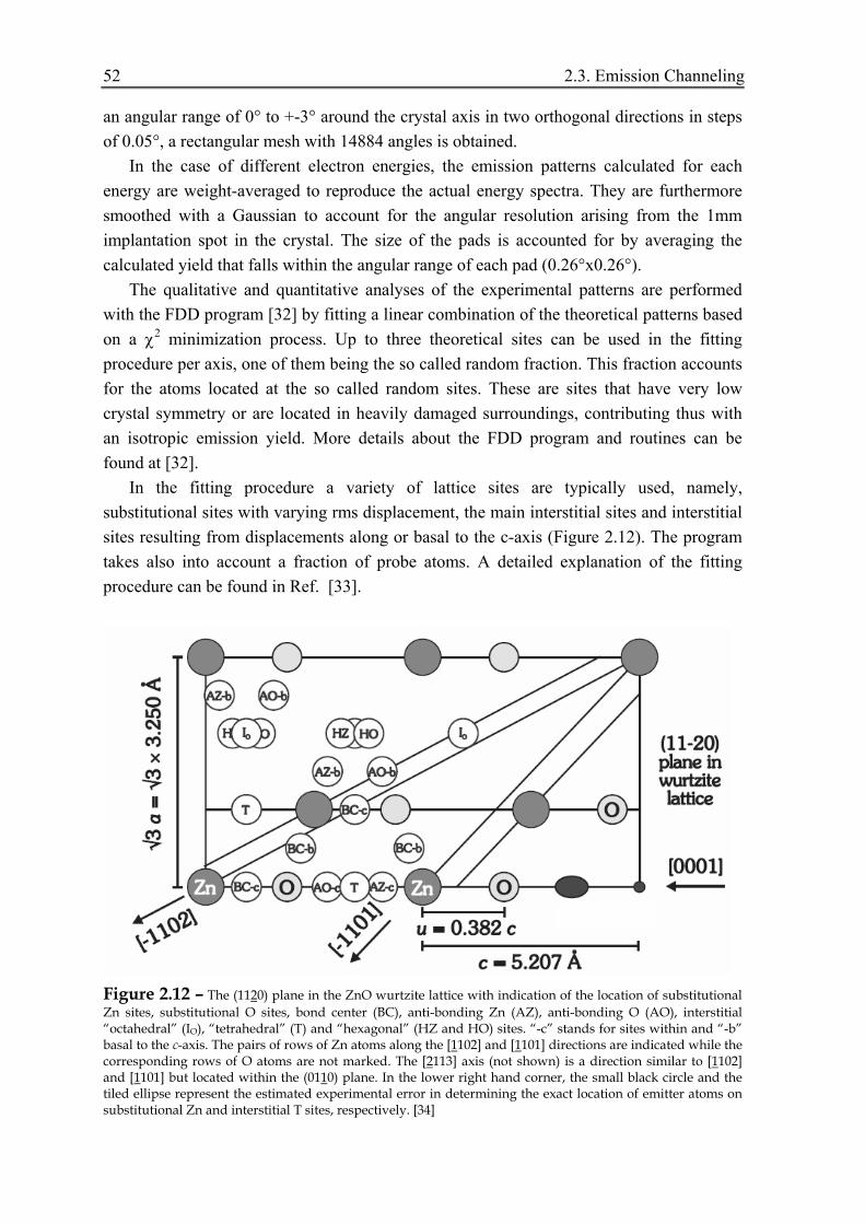
52 2.3. Emission Channeling
an angular range of 0° to +-3° around the crystal axis in two orthogonal directions in steps of 0.05°, a rectangular mesh with 14884 angles is obtained.
In the case of different electron energies, the emission patterns calculated for each energy are weight-averaged to reproduce the actual energy spectra. They are furthermore smoothed with a Gaussian to account for the angular resolution arising from the 1mm implantation spot in the crystal. The size of the pads is accounted for by averaging the calculated yield that falls within the angular range of each pad (0.26°x0.26°).
The qualitative and quantitative analyses of the experimental patterns are performed with the FDD program [32] by fitting a linear combination of the theoretical patterns based on a χ2 minimization process. Up to three theoretical sites can be used in the fitting procedure per axis, one of them being the so called random fraction. This fraction accounts for the atoms located at the so called random sites. These are sites that have very low crystal symmetry or are located in heavily damaged surroundings, contributing thus with an isotropic emission yield. More details about the FDD program and routines can be found at [32].
In the fitting procedure a variety of lattice sites are typically used, namely, substitutional sites with varying rms displacement, the main interstitial sites and interstitial sites resulting from displacements along or basal to the c-axis (Figure 2.12). The program takes also into account a fraction of probe atoms. A detailed explanation of the fitting procedure can be found in Ref. [33].
Figure 2.12 – The (1120) plane in the ZnO wurtzite lattice with indication of the location of substitutional Zn sites, substitutional O sites, bond center (BC), anti-bonding Zn (AZ), anti-bonding O (AO), interstitial “octahedral” (IO), “tetrahedral” (T) and “hexagonal” (HZ and HO) sites. “-c” stands for sites within and “-b” basal to the c-axis. The pairs of rows of Zn atoms along the [1102] and [1101] directions are indicated while the corresponding rows of O atoms are not marked. The [2113] axis (not shown) is a direction similar to [1102] and [1101] but located within the (0110) plane. In the lower right hand corner, the small black circle and the tiled ellipse represent the estimated experimental error in determining the exact location of emitter atoms on substitutional Zn and interstitial T sites, respectively. [34]

2.3.5 Data analysis 53
The above referred fitting procedure yields the lattice site location of the emitter atom and the fraction of those atoms at a given lattice site. However, the percentages resulting from the analysis program are not corrected for the scattered electrons. These are emitted electrons which are scattered by the walls of the experimental chamber into the detector. These electrons contribute positively to the random fraction, decreasing therefore the fractions at regular sites. The correction is applied to the fractions by means of a correction factor calculated with Monte-Carlo simulations of the background inside the EC experimental chamber [35] [36]. The correction factors depend on the angle between the sample normal and the detector, i.e., depend on the analyzed crystalline direction, so not all patterns are influenced in the same way. Typically, for the case of the experiments presented in this work, the fractions at regular sites resulting directly from the FDD program were increased by a factor of two following the correction. The error introduced by this procedure is around 10%. The values that will be presented in the results are already background corrected.
2.4. Perturbed Angular Correlations Perturbed Angular Correlations (PAC) is a well known and powerful technique for the
microscopic investigation of solid state properties. More precisely, it is particularly useful in the evaluation of charge distributions and magnetic fields inside a solid. Such fields result from the lattice structure and they can be disturbed by the presence of particular point defects. PAC makes use of the interaction between these fields and the magnetic dipole and/ electric quadrupole moments of a probe nucleus. In this way, valuable information about the probe’s local environment, in particular of near interacting point defects, is obtained.
In what follows, only a brief description of the theoretical and experimental aspects of the PAC technique is presented, since this is a well established method explained already with great detail in the literature.
2.4.1 General aspects The first step to perform a PAC experiment is to introduce inside the material under
study a radioactive isotope that will act as a probe. The basic principle of angular correlation lays in the fact that the probability of radiation emission from a radioactive nucleus depends on the angle between the emission direction and the nuclear spin direction. In a regular situation the spins of the nuclei are randomly distributed for which the radiation arising from a radioactive sample is isotropically emitted, i.e., the emission probability is the same in every direction. In contrast, an anisotropic emission is achieved
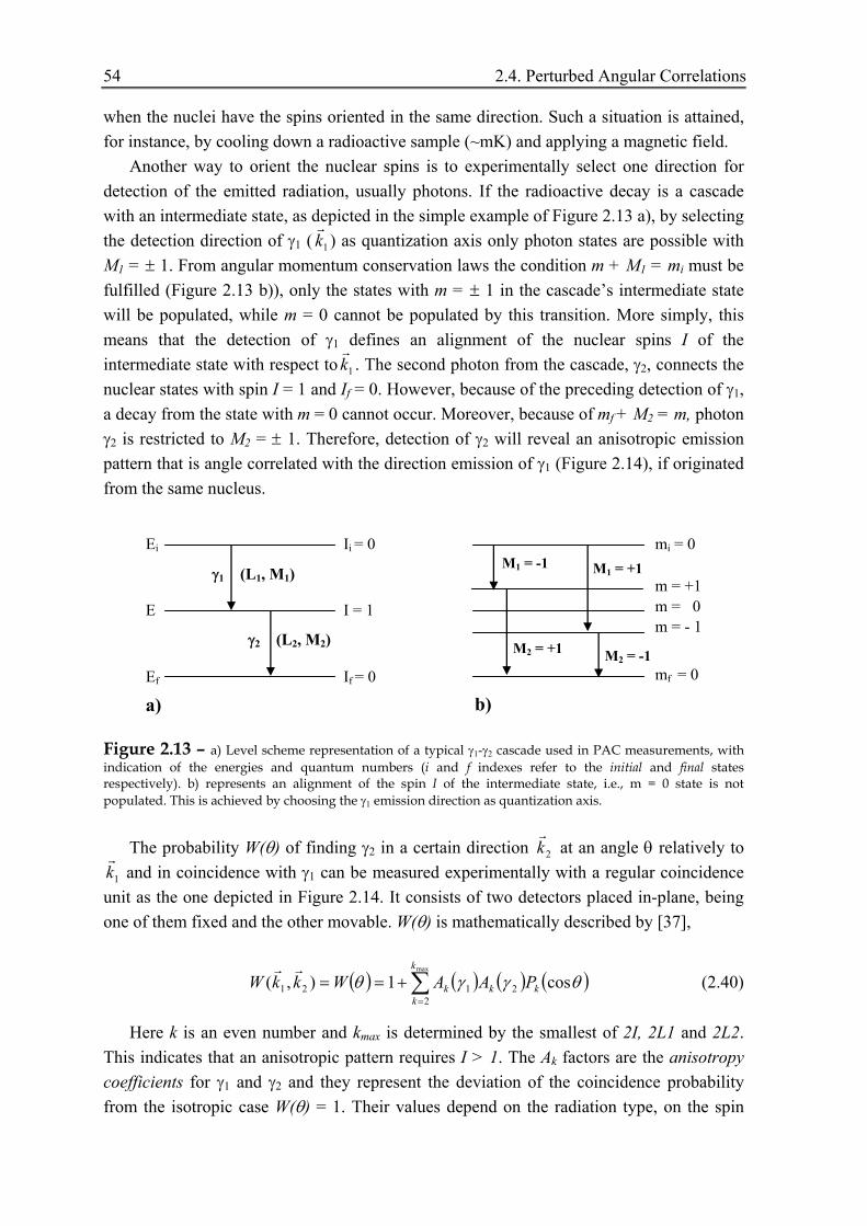
54 2.4. Perturbed Angular Correlations
when the nuclei have the spins oriented in the same direction. Such a situation is attained, for instance, by cooling down a radioactive sample (~mK) and applying a magnetic field.
Another way to orient the nuclear spins is to experimentally select one direction for detection of the emitted radiation, usually photons. If the radioactive decay is a cascade with an intermediate state, as depicted in the simple example of Figure 2.13 a), by selecting the detection direction of γ1 ( 1k
r) as quantization axis only photon states are possible with
M1 = ± 1. From angular momentum conservation laws the condition m + M1 = mi must be fulfilled (Figure 2.13 b)), only the states with m = ± 1 in the cascade’s intermediate state will be populated, while m = 0 cannot be populated by this transition. More simply, this means that the detection of γ1 defines an alignment of the nuclear spins I of the intermediate state with respect to 1k
r. The second photon from the cascade, γ2, connects the
nuclear states with spin I = 1 and If = 0. However, because of the preceding detection of γ1, a decay from the state with m = 0 cannot occur. Moreover, because of mf + M2 = m, photon γ2 is restricted to M2 = ± 1. Therefore, detection of γ2 will reveal an anisotropic emission pattern that is angle correlated with the direction emission of γ1 (Figure 2.14), if originated from the same nucleus.
Figure 2.13 – a) Level scheme representation of a typical γ1-γ2 cascade used in PAC measurements, with indication of the energies and quantum numbers (i and f indexes refer to the initial and final states respectively). b) represents an alignment of the spin I of the intermediate state, i.e., m = 0 state is not populated. This is achieved by choosing the γ1 emission direction as quantization axis.
The probability W(θ) of finding γ2 in a certain direction 2k
r at an angle θ relatively to
1kr
and in coincidence with γ1 can be measured experimentally with a regular coincidence unit as the one depicted in Figure 2.14. It consists of two detectors placed in-plane, being one of them fixed and the other movable. W(θ) is mathematically described by [37],
( ) ( ) ( ) ( )∑=
+==max
22121 cos1),(
k
kkkk PAAWkkW θγγθ
rr (2.40)
Here k is an even number and kmax is determined by the smallest of 2I, 2L1 and 2L2. This indicates that an anisotropic pattern requires I > 1. The Ak factors are the anisotropy coefficients for γ1 and γ2 and they represent the deviation of the coincidence probability from the isotropic case W(θ) = 1. Their values depend on the radiation type, on the spin
a)
Ei
E
Ef
γ1 (L1, M1)
γ2 (L2, M2)
Ii = 0
I = 1
If = 0
M1 = -1 mi = 0
m = +1 m = 0 m = - 1
mf = 0
M1 = +1
M2 = +1 M2 = -1
b)

2.4.1 General aspects 55
states of the cascade levels, on the multipolarity of the radiation and, in the case of non-pure transitions, on the mixing ratios. The Ak factors can be positive, negative or zero and can be found in tables [38]. The Pk’s are Legendre polynomials which describe the spatial angular distribution of the involved radiation. There are cases where a γ−γ angular correlation measurement is not feasible, for instance, if internal conversion is the main way of de-excitation. If so, the conversion electrons emitted in the radioactive cascade can be used to perform e--γ, γ-e- or e--e- angular correlations. This is achieved by replacing the γ detector by an electron detector. The Ak factors in equation 2.40 must then be multiplied by the particle parameter bk(e-) which can also be found in tables [38].
Figure 2.14 – Experimental setup to measure the γ-γ angular correlation W(θ), represented at the right hand side.
As referred previously, when the radioactive nuclei are inside a material, the magnetic μI and quadrupolar QI nuclear moments of the intermediate state will interact with magnetic fields or with the electric field gradients (EFG) created by the charge distribution that surrounds the probe nucleus. This interaction will cause a precession with frequency ω of the aligned nuclear spins I, which will also induce a time dependent precession of the γ2 anisotropic emission pattern W(θ, t). The ω values correlate with the hyperfine fields in the immediate vicinity of the probe nuclei which are function of its interaction with the host lattice and/or point defects.
In fact, what is observed experimentally is the time structure of the emission pattern W(θ, t), where t is the time delay between the emission of γ1 and the emission of γ2. During this time delay, the population of each state in the cascade changes due to the interaction with the hyperfine fields, which in turn will introduce a time variation of the γ2 angular emission pattern. The perturbed angular correlation (PAC) technique is precisely the evaluation of the above referred time perturbation. The mathematical description of W(θ, t) depends both on the type of interaction (magnetic or quadrupole) and on the type of samples (single-crystals or polycrystals).
0 90 180
W (θ
)
Detector angle θ
γ1
γ2
Coincidence W(θ)
D1
D2
θ 1kr
2kr

56 2.4. Perturbed Angular Correlations
The simplest form of the perturbed angular correlation function is found for polycrystalline samples, where the hyperfine fields are considered to be randomly oriented. In this case, W (θ, t) is described by [39],
( ) ( ) ( ) ( ) ( )∑=
−=
max
021 cos,
k
kkkkkk
t
PtGAAetW θγγθ τ (2.41)
where τ is the lifetime of the intermediate state and Gkk (t) is the perturbation factor which contains all information about the hyperfine fields with which the probe nucleus interacts. The main goal of PAC is to determine the Gkk(t) function so that the material properties can be accessed. A general formulation of Gkk(t) can be found at [39] which can be interpreted as a superposition of several harmonics of a fundamental frequency related with the hyperfine fields. The shape of Gkk(t), dependent on the interaction type, will be briefly described in what follows. 2.4.1.1 Electric Quadrupole Interaction
The electric quadrupole interaction results from the coupling of the probe nucleus
quadrupole moment with the hyperfine EFG and it is represented by the Hamiltonian,
∑=αβ
αβαβVQH Q 61
(2.42)
Here, Qαβ represents the quadrupole moment tensor given by,
( )( )∫ −= 3212
321 3,, dxdxdxrxxxxxQ N αββααβ δρ (2.43)
where ρN is the nuclear charge density. The EFG tensor Vαβ is a consequence of the exterior charge distribution that surrounds the probe nucleus and is represented by [4],
( ) αβαβαβαβ δΦ−Φ= TrV31
(2.44)
where Φαβ is the potential created by the charge distribution,
Φαβ = (δ2Φ)/(δxα δxβ) (2.45)
The EFG tensor is symmetric and, therefore, its eigenvalues are always real. Moreover, it is defined as the “principal EFG referential”, the system of axis where Vαβ is diagonal, by defining:
|VZZ| ≥ |VYY| ≥ |VXX| (2.46)

2.4.1 General aspects 57
This is a traceless tensor since the entire charge is considered as being external to the nucleus. In this way, only two independent components are needed to calculate the three eigenvalues. More precisely, the largest eigenvalue VZZ and the asymmetry parameter
η = (VXX - VYY)/ VZZ (2.47)
are generally used. This last parameter defines the deviation of the local charge distribution from the axial symmetric configurations (η = 0). Non-axial symmetric charge distributions will yield 1 ≥ η > 0 and they can result from the lattice structure itself or from the presence of point defects. For instance, in the case of ZnO, the EFG arising from the lattice structure (wurtzite) results in η = 0 along the [0001] direction due to the axial symmetry of the lattice.
The EFG interaction lifts off the m states degeneracy of the intermediate nuclear level with respect to |m|, originating an energy splitting ΔEn that is not necessarily equidistant. The radiative transitions between the m sub-levels will result in different spin precession frequencies ωn that can be observed experimentally (Figure 2.15).
Figure 2.15 – Electric quadrupole energy splitting for spin I = 5/2 of the intermediate state, caused by an interaction with an EFG. In this case, the three different energy transitions will result in three different observable frequencies (ω1, ω2 and ω3).
For a symmetric quadrupole interaction and if the principal EFG axis is defined as the quantization axis, the Hamiltonian is described by [4],
Hm,n = ħ ωQ (3m2 – I (I + 1)) (2.48)
where ωQ is the quadrupole frequency,
( )h124 −=
IIeQVzz
Qω (2.49)
The energy splitting, same is to say, the transition energies are described by,
|E0(m’) - E0(m)| = 3 |m’2 - m2| ħ ω0 (2.50)
I = 5/2
m = ± 5/2
m = ± 3/2
m = ± 1/2 ΔE1
ΔE2 ΔE3

58 2.4. Perturbed Angular Correlations
Usually, the fundamental observable frequency of the interaction is defined as,
ω0 = ΔE / ħ (2.51)
where ΔE is the smallest of the transition energies. This relates with ωQ through,
ω0 = 3ωQ for I integer (2.52)
ω0 = 6ωQ for I half-integer (2.53)
The number of frequencies observed experimentally depends on the spin of the intermediate level. For instance, an intermediate state with I = 5/2 is split by a pure electric quadrupole interaction into three different energy levels (Figure 2.15), giving rise to three different observable frequencies in the PAC spectrum (ω1, ω2 and ω3 = ω1+ω2). This is actually the situation patent in the experimental results presented in Chapter 4, since 111Ag and 111In were used in these studies as PAC radioactive probes. In both cases, the PAC measurements were performed in an intermediate state with I = 5/2+, leading thus to three observable frequencies in the experimental spectrum.
The perturbation factor Gkk(t) for the electric quadrupole interaction is given by,
( ) ( )∑=
=max
00cos
n
nknkk tnstG ω (2.54)
where the skn factors are the amplitudes of the observable frequencies. Another parameter frequently used to define the strength of the EFG is the fundamental
quadrupole frequency νQ also called coupling constant described as,
( )
KII
heQVzz
Q πω
ν2
124 0 −== (2.55)
where K=3 for I integer and K=6 for I half-integer. 2.4.1.2 Magnetic Dipole Interaction
Since there are no hyperfine magnetic fields in ZnO single-crystals, a brief description
of the magnetic dipole interaction will be presented, for complement only. In this case the Hamiltonian results from the interaction of the probe nucleus magnetic dipole moment μ with the hyperfine magnetic field B yielding,

2.4.1 General aspects 59
∑−=⋅−=α
ααmag BI γBμH h (2.56)
Here =μr γ ħ Ir
with Ir
representing the nuclear spin operator and γ the gyromagnetic ratio given by,
hNg
μγ = (2.57)
where the g-factor is dimensionless. Similarly to the EFG interaction, the magnetic dipole interaction also lifts the m states
degeneracy of the intermediate state. However, in this case the splitting is energetically equidistant (Zeeman splitting) and the degeneracy is lift off with respect to the signal of m. Since only transitions between neighboring states are allowed we get for the energy transitions,
ΔE = Em+1 – Em = -γ ħ Bz (2.58)
As an outcome, only one transition frequency will be observed experimentally, the
Larmor frequency ωL,
ωL = ΔE / ħ = -γ Bz (2.59) The perturbation factor for a pure magnetic dipole interaction in a polycrystalline
sample (magnetic domains random orientation) is then described by,
( )( )
12k
tnωcos21tG
k
1nL
kk +
+=
∑= (2.60)
2.4.1.3 Single-crystals features
The formalism above presented is generally applicable for polycrystalline samples,
with random orientation of the EFGs or magnetic fields. However, PAC can be used to study single-crystals allowing, in principle, the determination of the EFG orientation, its intensity and symmetry with respect to the axis of symmetry of the crystalline lattice. In this way, nearby point defects can be better characterized, helping on model simulations.
For a single-crystal, equation 2.41 is no longer applicable since the angles that the emission directions of γ1 ( 1k
r) and γ2 ( 2k
r) form with the VZZ component of the EFG must
be taken into account. Moreover, W(θ, t) has to be calculated separately for each detector arrangement. In fact, Equation 2.41 presented earlier is a simplification for polycrystalline

60 2.4. Perturbed Angular Correlations
samples which results from the more general perturbed angular correlation function given by [39],
(2.61 a))
with the perturbation factor given by [39],
⎟⎟⎠
⎞⎜⎜⎝
⎛−⎟⎟
⎠
⎞⎜⎜⎝
⎛−
×++−= ∑ ++
2
2'
1
1'21
22121 1212)1()(
Nk
mI
mI
Nk
mI
mI
kktGbbaa
mbma
mbmaINNkk (2.61 b))
∗ΛΛ× '' |)(||)(|
abmtmmtm ab
These equations are applicable when the magnetic field or the EFG have the same
orientation with respect to the detectors for all the nuclei in the intermediate excited state of the decaying cascade. More precisely, they are valid for external fields and single-crystals where the point defects obey to some regular orientation inside the crystals.
In Equations 2.61, Λ(t) = exp[(-i/ħ) H(t)] is the time evolution operator for static interactions. H(t) is the Hamiltoniam describing the interaction of the intermediate nuclear state with its environment via its nuclear dipole or quadrupole moment (presented earlier). The angles θ1, ϕ1 and θ2, ϕ2 are associated with the emission directions 1k
rand 2k
rwithin the
axis system S (Figure 2.16) for the case of two detectors. For an electric quadrupole interaction, S is the main EFG referential where the EFG tensor (Vαβ) is diagonal and verifies |VZZ| ≥ |VYY| ≥ |VXX|. For a magnetic interaction, S is defined in such a way that the z axis is collinear with the magnetic field.
Figure 2.16 – Axial system S where the angles between the photon emission directions ( 1k
r , 2kr ) and the
EFG (or magnetic field) orientation are defined.
Z
X Y
D2 D1
1kr
2kr
θ 1 θ 2
ϕ 1 ϕ 2
Referential S
∑ ∑ ∗− ×++
21
21
222
2111
121
2121
2211/21 ),(),()(
2212)()(
~),,(kk
NN
Nk
Nk
NNkk
kkt YYtGkk
AANetkkW ϕθϕθ
γγτrr

2.4.2 Experimental setup 61
In single-crystals, the EFG (or magnetic field) orientation, intensity and symmetry relatively to the crystal symmetry axis can be determined via evaluation of the amplitude and frequency of the perturbation functions 21
21NN
kkG . On a PAC measurement, the main difference between a polycrystalline sample (presented above) and a single-crystal shows up in the skn amplitudes, but not on the values of the observable frequencies ω0n, since these only depend on the levels energy splitting. The fact that the EFG principal component has a well defined orientation will result in different relative amplitudes of the observable frequencies, depending on the sample’s orientation relatively to the detectors [40].
2.4.2 Experimental setup The γ−γ PAC experiments reported in this work were performed using an experimental
apparatus composed by 4 BaF2 detectors, arranged in the same plane, at 90º with each other (Figure 2.17). Since all detectors send a start (γ1 detection) and stop (γ2 detection) signal, twelve coincidence time spectra can be collected in a single measurement (4 at 180° and 8 at 90° since all detectors ), which are afterwards combined to yield the experimental R(t) ratio (presented ahead in section 2.4.3).
EFG
ZnO (seen from above)
D3
D1
D2D4
ϕ = 45°θ = 0°
EFG
ZnO (seen from above)
D3D3
D1D1
D2
D2D4
D4
ϕ = 45°θ = 0°
Figure 2.17 – Scheme of an in- plane 4- BaF2 detector setup used in the γ−γ PAC measurements.
All measurements were carried out at room temperature. The ZnO single-crystals were
mounted in the center of the detectors using a special sample holder that allowed the orientation of the crystal relatively to the detectors. This is very important to correctly determinate the EFGs orientations. In this sense, the ZnO samples were placed in the

62 2.4. Perturbed Angular Correlations
upright position, with the [0001] direction (surface direction) making 45º with all the detectors (Figure 2.17). For an unperturbed (η= 0) ZnO single-crystal the main component (VZZ) of the EFG resulting from the lattice symmetry is oriented along the [0001] direction. Therefore, this experimental geometry is equivalent to place the lattice EFG (VZZ principal system of axis) at 45º with all the detectors.
For the particular case of single-crystals, it is important to define the EFG direction (EFG system) relatively to the detectors (laboratory system), so that the EFG orientation can be correctly determined. This relationship is made via three angles: theta (θ), phi (ϕ) and rho (ρ) which are defined in a three-detector setup (restriction associated with the fitting program NNFIT [41] [42] described in section 2.4.3). These angles are represented in Figure 2.18, where ABC represents the lab system and XEFGYEFGZEFG is the EFG system. More precisely, the EFG components VXX, VYY and VZZ are considered as being aligned along XEFG, YEFG and ZEFG, respectively. In this way, θ is basically the angle between the VZZ and the detector’s plane, and ϕ is the angle between the VZZ projection in the detectors plane and the start detector. These two angles define the ZEFG axis, that is, they define the VZZ orientation. Then, ρ is a rotation of the XEFGYEFG plane around ZEFG (refer to Figure 2.18).
Figure 2.18 – Definition of the EFG system axis (XEFG, YEFG, ZEFG) relatively to the lab system (A, B, C) through angles theta (θ), phi (ϕ) and rho (ρ). Here, a three-detector setup is represented since these angle definitions are used in the data fitting software NNFIT (section 2.4.3), which is based in setups with this configuration. Refer to the text for a detailed explanation of the angles.
Given these angle definitions, it is now easier to describe the ZnO sample’s position
relatively to the detectors: the lattice EFG (along the [0001] crystallographic direction) is oriented according to θ = 0º and ϕ = 45º (Figure 2.17). This means that the main component VZZ is in-plane with the detectors. The ZnO single-crystals were placed in this position in all the PAC measurements presented in this dissertation.
C
A
ZEFG = VZZ
θ
ϕ
ρ
B
- A
YEFG
ρ XEFG

2.4.3 PAC experimental function and data analysis 63
2.4.3 PAC experimental function and data analysis PAC experimental function The aim of the PAC technique is to determine the perturbation factor Gkk (t) (for single-crystals) that contains all the information regarding the hyperfine fields. To do so, one has firstly to measure the coincidence count rate N, at a fixed detector angle, as a function of the time elapsed between the emission of γ1 and γ2 from the decay cascade. That is, the N(θ,t) function has to be determined.
The coincidence count rate is measured with a PAC apparatus that comprises several detectors arranged in such a way that the angle between any pair of detectors is 90º or 180º. In the experiments presented in Chapter 4, the 4-detector setup arrangement described in Figure 2.17 was used. To describe the physics behind the experimental apparatus lest first consider two detectors i and j. When a photon strikes a detector two signals are generated in the detector’s photomultiplier: a sharp anode signal that gives the information in time tγ, and a dynode signal that contains the energy information Eγ. If a γ-ray is detected in detector i, with the correct energy Eγ1, a clock is started. Then, when a second γ-ray, with the correct energy Eγ2, reaches the other detector j the clock is stopped and this coincidence event will be stored in the coincidence counter of the (i, j) pair of detectors.
The experimental coincidence count rate for the (i, j) pair of detectors is given by,
(2.62)
where t = tγ2 - tγ1 is the time elapsed between the emission of γ1 and γ2 and θ is the angle between the two detectors. N0 is proportional to the number of radioactive nuclei present in the sample and B is the time-independent background which is proportional to the events due to chance coincidences (coincidences arising from different nucleus). Finally, W(θ,t) is the perturbed angular correlation function (Equation 2.41 for polycrystals and Equation 2.61 for single-crystals).
Once the coincidence time histogram between detectors is determined, the PAC experimental function Rexp(t) can be constructed. This function is the main experimental quantity that provides all the relevant information. To construct Rexp(t,) several spectra registered at θ = 90° and θ = 180° are combined, to remove the exponential decay and reveal the R(t) function. More precisely, after the background B subtraction, all the coincidence count rates Nij(θ,t), resulting from detectors with the same angular separation, are averaged: N(θ,t) = θ θN
ij ij tN∏ ),( . Here, Nθ is the total number of spectra for a certain
angle of detectors. The experimental Rexp (t) PAC function is then obtained,
),90(2),180(),90(),180(2)(exp tNtN
tNtNtR°+°
°−°= (2.63)
( ) ( ) Btθ,WeNtθ,N τt
0ij +=−
64 2.4. Perturbed Angular Correlations
It is relevant to mention that systematic efficiency errors are corrected via the geometric average of all spectra acquired at the same detector’s angle. Also important is that the measurable experimental quantity Rexp (t) is related with the perturbation factor
2121NN
kkG (t), which contains information about the hyperfine fields.
Data analysis To extract quantitative information from the PAC spectrum the experimental data is fitted with a theoretical function Rfit (t), through which the perturbation factor Gkk (t) is also calculated. The fitting procedure is carried out with a computer software developed by N. Barradas [41] [42]. The theoretical functions that the program calculates correspond to a three-detector setup, all in the same plane at 90º with each other (Figure 2.19). To simulate four-detector spectra, the three-detector spectra must be combined according to the stratagem described in [41] and [42].
The program firstly calculates the eigenvalues and eigenstates of the Hamiltonians for the electric quadrupole interaction (equation 2.42) and for the magnetic dipole interaction (equation 2.56). The finite time resolution of the PAC setup is also accounted in this calculation by multiplying each term of the sum of the perturbation factor Gkk (t) by
),( *iWHMFP ω ,
⎟⎟⎠
⎞⎜⎜⎝
⎛−=
2ln16exp),(
2*2* WHMi
iWHMF
FPω
ω (2.64)
where FWHM* is associated with the time resolution function of the spectrometer, which is represented by a gaussian prompt function. Moreover, possible frequency distributions are considered by multiplying the Gkk (t) terms by the distribution’s Fourier transform Dgaussian (FWHM, t). These frequency distributions result from the presence of lattice defects, which produce slightly different EFG values in the probes neighborhood. This means that instead of a well defined hyperfine EFG, the probes sense a distribution of these hyperfine fields. In the frequency space (Fourier spectrum) these distributions can be represented by a gaussian or lorentzian distribution. The outcome of this scenario is the attenuation of the PAC spectrum amplitude in the time space which is represented mathematically by,
Dgaussian (FWHM, t) =2
2
2ln16t
FWHM
e−
for a gaussian distribution (2.65a)
Dlorentzian (FWHM, t) =tFWHM
e 2−
for a lorentzian distribution (2.65b)
where FWHM represents the distribution Full Width Half Maximum. For a gaussian distribution the standard deviation σ = FWHM/ 2ln8 is usually used to describe the frequency broadening, instead of the FWHM.
The perturbation factor ( )tGfitkk resulting from this fitting procedure is thus,

2.4.3 PAC experimental function and data analysis 65
( ) ( )∑=
∗=maxn
0niWHMWHMntgauss/lore0kn
fitkk )ω,P(F t),(FD tnωcosstG (2.66)
The correspondent perturbed angular correlation functions Wfit (θ, t) are then calculated for θ = 90º and θ = 180º. The fit function, whose parameters are fitted to the experimental Rexp (t) is then described by,
,t)( W,t)(W,t)(W,t)(W
(t)Rfitfit
fitfitfit °+°
°−°=
90218090180
2 (2.67)
An important remark must be made at this point. In the equations above presented, θ
represents the angle between the detectors (90º or 180º). This angle should not be confused with the angles defined in Figure 2.18 for single-crystals (θ, ϕ and ρ) which describe the EFG orientation relatively to the detectors setup. Actually, these EFG-related angles were used as input fit parameters in the fitting procedure, since in this work PAC was used to study ZnO single-crystals. This angle information influences the final amplitudes skncos(ωt) at the end of the fit, which is important since, as referred earlier, different relative amplitudes of the observable frequencies are observed in the Fourier transform of the experimental spectrum, depending on the EFG orientation relatively to the detectors. In this work three observable frequencies are observed in the experimental Rexp(t) spectrum since the PAC measures were performed in a intermediate state with I = 5/2+. However, since their amplitudes depend also on the EFG angles relatively to the detectors, there are some situations for which not all the observable frequencies are “seen” in the Fourier transform. These amplitudes depend also on the charge axial asymmetry, that is, on the value of η. Several examples are presented in Figure 2.19. These are simulations for different angles and different η, obtained via the PAC fitting program above referred.
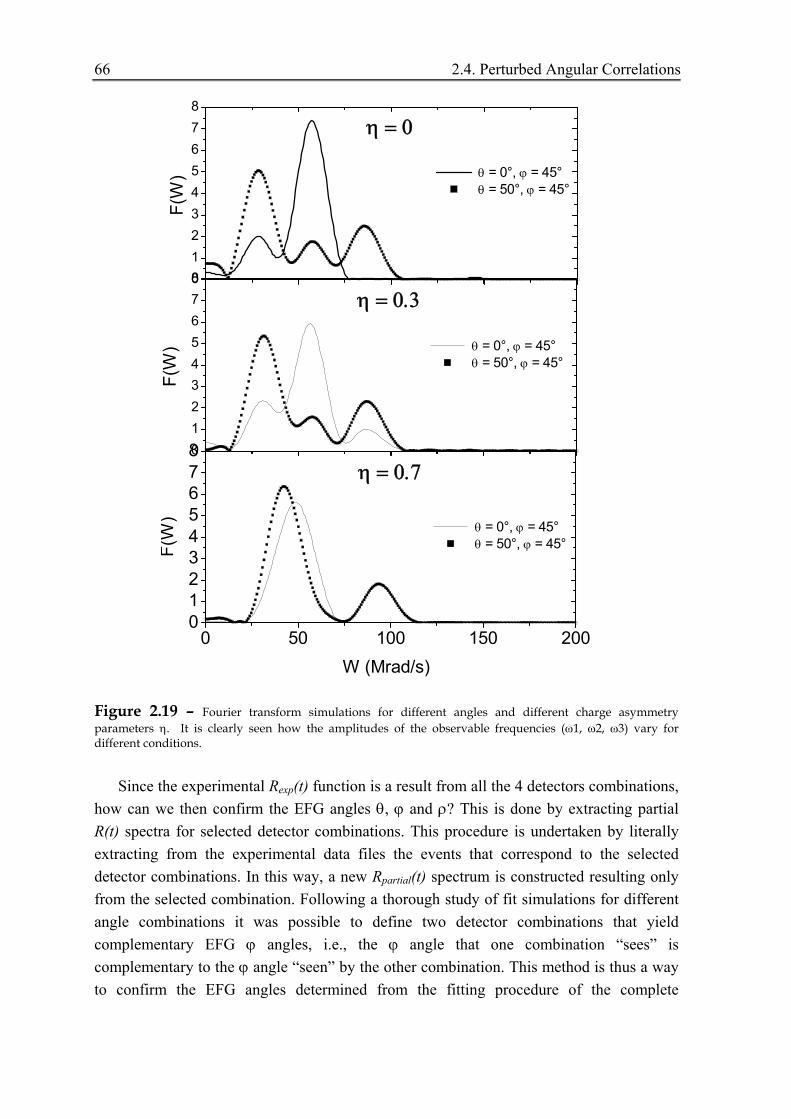
66 2.4. Perturbed Angular Correlations
012345678
012345678
0 50 100 150 200012345678
η = 0
F(W
) θ = 0°, ϕ = 45° θ = 50°, ϕ = 45°
θ = 0°, ϕ = 45° θ = 50°, ϕ = 45°
η = 0.3
F(W
)
θ = 0°, ϕ = 45° θ = 50°, ϕ = 45°
η = 0.7
F(W
)
W (Mrad/s)
Figure 2.19 – Fourier transform simulations for different angles and different charge asymmetry parameters η. It is clearly seen how the amplitudes of the observable frequencies (ω1, ω2, ω3) vary for different conditions.
Since the experimental Rexp(t) function is a result from all the 4 detectors combinations,
how can we then confirm the EFG angles θ, ϕ and ρ? This is done by extracting partial R(t) spectra for selected detector combinations. This procedure is undertaken by literally extracting from the experimental data files the events that correspond to the selected detector combinations. In this way, a new Rpartial(t) spectrum is constructed resulting only from the selected combination. Following a thorough study of fit simulations for different angle combinations it was possible to define two detector combinations that yield complementary EFG ϕ angles, i.e., the ϕ angle that one combination “sees” is complementary to the ϕ angle “seen” by the other combination. This method is thus a way to confirm the EFG angles determined from the fitting procedure of the complete
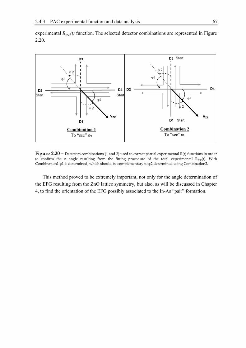
2.4.3 PAC experimental function and data analysis 67
experimental Rexp(t) function. The selected detector combinations are represented in Figure 2.20.
Figure 2.20 – Detectors combinations (1 and 2) used to extract partial experimental R(t) functions in order to confirm the ϕ angle resulting from the fitting procedure of the total experimental Rexp(t). With Combination1 ϕ1 is determined, which should be complementary to ϕ2 determined using Combination2.
This method proved to be extremely important, not only for the angle determination of
the EFG resulting from the ZnO lattice symmetry, but also, as will be discussed in Chapter 4, to find the orientation of the EFG possibly associated to the In-As “pair” formation.
D3
D1
D4D2Start Start
VZZ
ϕ1
ϕ1
ϕ 2
ϕ 2
Vou ver ϕ1Combination 1 To “see” ϕ1
D3
D1
D4D2
Start
Start
Vou ver ϕ2
ϕ1
ϕ1
ϕ 2
ϕ 2
VZZ
Combination 2 To “see” ϕ2

Bibliography [1] – W. Chu, J.W. Mayer and M. Nicolet, Backscattering Spectrometry, Academic Press,
(1978) [2] – W. Chu, New Uses of Ions Accelerators, Capítulo 2, Plenum Press, (1975) [3] – L. C. Feldman and J. W. Mayer, Fundamentals of surface and thin film analysis,
Elsevier Science Publishers, 1986 [4] – G. Schatz and A. Weidinger, Nuclear Condensed Matter Physics, John Wiley & Sons
Ltd., England (1996) [5] – http://tpvcell.hmg.inpg.fr/ITN.html [6] – E. Kugler, D. Fiander, B. Jonson, H. Haas, A. Przewloka, H.L. Ravn, D.J. Simon, K.
Zimmer, and the ISOLDE collaboration, Nucl. Instrum. Meth. Phys. Res. B 70, 41 (1992)
[7] – B. Domeji and K. Bjorkqvist, Phys. Lett. 14, 127 (1965) [8] – R.S. Nelson and M.W. Thompson, Phil. Mag. 8, 1677 (1963) [9] – C. Lehmann and G. Leibfried, J.Appl. Phys. 34, 2821 (1963) [10] – J. Lindhard, Mat. Fys. Medd. 34, 1 (1965) [11] – C. Erginsoy, Phys. Rev. Lett. 15, 360 (1965) [12] – E. Uggerhøj, Phys. Lett. 22, 382 (1966) [13] – G. Astner, I. Bergström, B. Domeji, I. Erikson and A. Persson, Phys. Lett. 14, 308
(1965) [14] – U. Wahl, Phys. Rep. 280, 146 (1997) [15] – U. Wahl, A. Vantome, J. De Wachter, R. Moons, G. Langouche, J.G. Marques and
J.G. Correia, Phys. Rev. Lett. 79, 2069 (1997)

Bibliography 69
[16] – U. Wahl, A. Vantome, G. Langouche, J.P. Araújo, L. Peralta, and J.G. Correia, Appl. Phys. Lett. 77, 2142 (2000)
[17] – J.P. Araújo, Ph. D. Thesis, Fac. de Ciências da Universidade do Porto, Porto (2001) [18] – E. Uggerhøj and F. Frandsen, Phys. Rev. B 2, 582 (1970) [19] – F. Fujimoto, S. Takagi, K. Komaki, H. Koike and Y. Uchida, Radiat. Eff. 12, 153
(1972) [20] – H. Hofsäss and G. Lindner, Phys. Rep. 201, 121 (1991) [21] – J.U. Andersen, E. Bonderup, E. Laegsgaard, B.B. Marsh and A.H. Sørsensen, Nucl.
Instrum. Meth. 194, 209 (1982) [22] – P.A. Doyle and P.S. Turner, Acta Crys. A 24, 390 (1968) [23] – N.W. Ashcroft and N.D. Mermim, Solid State Physics, Saunders College Publishing
(1976) [24] – J.U. Andersen, S.K. Andersen and W.M. Augustyniak, K. Dan. Vidensk. Selsk. Mat.
Fys. Medd. 39, no.10 (1977) [25] – B.T.M. Willis and A.W. Pryor, Thermal vibrations in Crystallography, Cambridge
University Press, Cambridge, (1975) [26] – P.G. Dawer and R.J. Elliot, Proc. Roy. Soc. London A273, 222 (1963) [27] – U. Wahl, J.G. Correia, A. Czermak, S.G. Jahn, P. Jalocha, J.G. Marques, A. Rudge,
F. Schopper, J.C. Soares, A. Vantomme, P. Weilhammer and the ISOLDE collaboration, Nucl. Instrum. Meth. Phys. Res. A 524, 245 (2004)
[28] – P. Weilhammer, E. Nygård, W. Dulinski, A. Czermak, F. Djama, S. Gadomski, S.
Roe, A. Rudge, F. Schopper and J. Strobel, Nucl. Instrum. Meth. A 383, 89 (1996) [29] – U. Rössler, in Landolt-Börnstein New Series, Vol. 22, edited by O. Madelung
(Springer, Berlin, 1989), p. 163 [30] – H. Schulz and K.H. Thiemann, Solid State Comm. 32, 783 (1979) [31] – J.F. Ziegler and J.P. Biersack, The Stopping and Range of Ions in Matter, Pergamon
Press, New York (1985) [32] – U. Wahl, Ph. D. Thesis, Konstanz Univ., Konstanz (1992) [33] – U. Wahl, J.G. Correia, S. Cardoso, J.G. Marques, A. Vantomme, G. Langouche, and
the ISOLDE collaboration, Nucl. Instrum. Meth. B 136-138, 744 (1998)

70 Bibliography
[34] – U. Wahl, E. Rita, J. G. Correia, A. C. Marques, E. Alves, and J. C. Soares (ISOLDE Collaboration), Phys. Rev. Lett. 95, 215503 (2005)
[35] – B. De Vries, Ph. D. Thesis, Katholieke Universiteit Leuven and Instituut voor Kern-
en Stranlingsfysica (IKS), Leuven (2006) [36] – U. Wahl, A. Vantomme, G. Langouche, J.G. Correia and L. Peralta, Appl. Phys.
Lett. 78, 3217 (2001) [37] – H. Frauenfelder and R.M. Stefen, Alpha – Beta – and Gamma-ray spectroscopy,
Chapter XIX (A) 2, 997 (1965), ed. K. Siegbahn [38] – R.S. Hager et al., Nucl. Data A 4, 397 (1968) [39] – T. Butz, Hyp. Int. 52, 189 (1989) [40] – Th. Wichert and E. Recknagel, Microscopic Methods in Metals, Topics in Current
Physics 40 p. 317, U. Gonser ed., Springer-Verlag (1986) [41] – N.P. Barradas, M. Rots, A.A. Melo and J.C. Soares, Phys. Rev. B 47, 8763 (1993) [42] – N.P. Barradas, Ph. D. Thesis, Faculdade de Ciências da Universidade de Lisboa,
Lisboa (1994) [43] – R.P. Gupta and S.K. Sen, Phys Rev. A 8, 1169 (1973) [44] –P.C. Schmidt, K.D. Sen, T.P. Das and A. Weiss, Phys Rev. B 22, 4167 (1980) [45] – F.D. Feiock and W.R. Johnson, Phys Rev. 187, 39 (1969) [46] – P. Raghavan, E.N. Kaufmann, R.S. Raghavan, E.J. Ansaldo and R.A. Naumann,
Phys Rev. B 13, 2835 (1976)

Chapter 3
Samples Designation and Experimental Conditions
In this chapter, a resume of the ZnO samples designations, the ion implantation
parameters and the annealing treatments used in this work will be present.
3.1. Implantation parameters Table 3.1 refers to the ion implanted ZnO single-crystals intended for damage
annealing (section 4.1) and p-type doping (section 4.2) studies. In Table 3.2 the p-type dopants implantation parameters are depicted. The implantation details regarding the co-doping studies with In and As are resumed in a different table, namely, Table 3.3.
The ZnO 5×5 mm2 single-crystals were obtained from different companies, using different growth methods (SCVT or hydrothermal). Indeed, at an initial stage of the PhD the high quality ZnO single-crystals commercially available were the ones produced by “Eagle-Picher”. Unfortunately this enterprise came to an end at some point, for which the ZnO single-crystals from “Crystec” were used. These last single-crystals proved to be also of excellent crystalline quality. For all samples, the normal to the surface of the crystals was the [0001] direction.
The implantations of radioactive isotopes were carried out at ISOLDE (CERN) while the ones of stable isotopes were performed at ITN. Most of the crystals were implanted with a given tilt angle relatively to the incident beam in order to avoid channeled implantation.

72 3.1. Implantation parameters
Table 3.1 – Sample designation, im
plantation parameters and ZnO
single-crystals provenience for the samples used in the
damage annealing studies (section 4.1) and in the p-type dopants im
planted in ZnO (section 4.2).

3.1. Implantation parameters 73
Table 3.2 – Sample designation, im
plantation parameters and the provenience of the ZnO
single-crystals for the samples used in the
Rare-Earth studies presented in section 4.3.

74 3.1. Implantation parameters
Dose
EI
Range
Dose
EI
Range
(at/cm2)
(KeV
)( Å
)(at/cm
2) (K
eV)
( Å)
Crystal 1
E-C
21x10
1340
1431x10
14 ( 73As) *
30138
EC
E-C
51x10
13 ( 111In)**40
1431x10
1430
138P
AC
g-g
E-C
61x10
13 ( 111In) *40
1431x10
1430
138E
C
Stable elem
ents (implanted at ITN
) - swept beam
implantation
Radioactive elem
ents (implanted at C
ER
N)
* For EC
experiments the im
plantations were w
ith a 7º tilt angle and 1mm
beam spot
** For PA
C experim
ent the implantation beam
was sw
ept
Crystal 2
InAs
TechniquesSam
ples
Table 3.3 – Sample designation and im
plantation parameters for the ZnO
single-crystals used in the In and As
co-doping experiments presented in section 4.2.4.

3.2. Annealing treatments 75
3.2. Annealing treatments
Most of the ion implanted ZnO single-crystals were annealed in air and/or in vacuum to evaluate the dopant behavior and lattice recovery as a function of annealing temperature. The annealing treatments performed in each of the samples presented in sections 4.1 and 4.2 are resumed in Table 3.4, while for samples presented in section 4.3 can be found at table 3.5. For the co-doping experiments, the annealings can be found at table 3.6.
Notice that with one or two exceptions, the EC experiments annealings were performed in-situ, while the ones of PAC, RBS and PL were undertaken ex-situ using a tubular resistive furnace.
Table 3.4 – Annealing treatments performed on the ZnO single-crystals presented in sections 4.1 and 4.2.
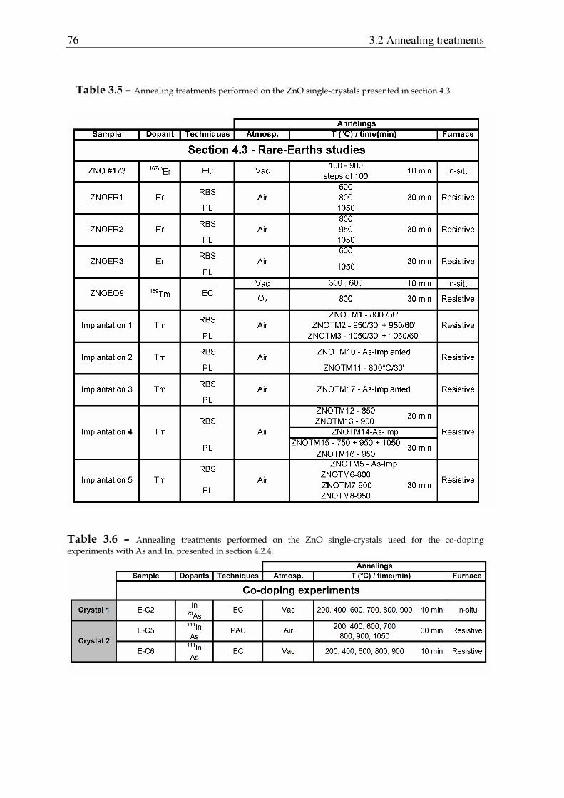
76 3.2 Annealing treatments
Table 3.5 – Annealing treatments performed on the ZnO single-crystals presented in section 4.3.
Table 3.6 – Annealing treatments performed on the ZnO single-crystals used for the co-doping experiments with As and In, presented in section 4.2.4.
Chapter 4
Results and discussion
In this chapter the author attempts to address some of the questions associated to the dopant behavior inside the ZnO single-crystal and to the role of defects and intrinsic impurities. Based on the experimental and theoretical studies carried out in the last four years, the discussion will focus on the results obtained for the studies of ZnO single-crystals ion implanted with n-type and p-type dopants and with optically active rare-earths. As mentioned in the Motivation, these are three of the main topics being studied nowadays in ZnO, due to their promising applications for optoelectronic devices.
The chapter is organized as follows:
4.1. – Implantation damage annealing Evaluation of the best damage annealing conditions for ZnO single-crystals implanted with Fe, Sr and Ca isotopes.
4.2. – Ion implanted p-type dopants in ZnO single-crystals
Investigation of the lattice site location and local environment of Cu, Ag and As elements ion implanted in ZnO. The co-doping of ZnO with In and As is also discussed.
4.3. – Lattice location and photoluminescent properties of RE implanted in ZnO
The lattice site location, optical activation and implantation damage recovery are addressed for the rare-earths Er and Tm ion implanted in ZnO.
4.1. Implantation damage annealing
Doping by ion implantation is always associated with a certain degree of lattice damage, which can influence the doping effects. In most of the cases, the damaged regions of the lattice have compensating effects which prevent the dopants from playing a desired role. A recovery of the lattice is therefore envisaged which can be achieved with thermal annealings. Given the theme of the PhD work described in this dissertation and the fact that

78 4.1. Implantation damage annealing
ion implantation was used in all the studies here presented the evaluation of implantation damage annealing is peremptory. In this sense, in what follows, implantation damage annealing is addressed as a function of annealing temperature and atmosphere (air Vs vacuum). This study starts with the investigation of the lattice recovery on a 57Fe implanted ZnO single-crystal, making use of Rutherford Backscattering Spectroscopy (RBS). Moreover, the lattice site location behavior of 89Sr and 45Ca (impurities isoelectronic to Zn) implanted on ZnO was evaluated by means of Emission Channeling (EC) as a function of annealing temperature.
4.1.1. 57Fe implanted ZnO single-crystal This section presents and discusses results obtained for damage annealing on a ZnO
single-crystal implanted with Fe. This investigation was carried out as a function of annealing temperature and for two different annealing atmospheres, namely, air and vacuum. The goal of this study is to find the optimum implantation damage annealing conditions for ZnO.
Experimental details A ZnO [0001] single-crystal was implanted at room temperature with 1×10¹⁶ at/cm2 of 57Fe at 100 keV. Following ion implantation the single-crystal was split in two (sample ZNOFE1 and ZNOFE2 in table 3.1 and table 3.4) so that two different annealing atmospheres could be studied (air Vs vacuum). Both crystals were subjected to 30 min 300°C, 600°C, 900°C and 1050°C annealing steps, but while ZNOFE1 was annealed in air, ZNOFE2 was annealed in vacuum. The lattice quality along the [0001] direction and for a random orientation was evaluated in both crystals in the as-implanted state and following each of the annealing steps by means of RBS, using a 2MeV 4He+ beam.
Results and discussion Figure 4.1 displays the progressive lattice recovery observed in both air and vacuum annealed samples. The inserted arrows indicate the surface edge position of each element. As can be seen, Zn masks the Fe signal, making impossible the study of this element with RBS. However, the implantation damage peak is well pronounced in the [0001]-aligned spectra revealing that the minimum yield (χmin) raised from 2% (virgin ZnO crystal) to 50%. Nevertheless, no amorphous region was found. Lattice recovery starts already at 300ºC with a χmin decrease to 43% (air annealing). Near complete lattice recovery is achieved at 1050°C in air (χmin = 3%), which is in agreement with previous studies performed following heavy ion implantation [1]. The lattice recovery in the vacuum annealed sample (sample ZNOFE2) follows the same trend, but with a slightly higher residual damage following each annealing step. A χmin of 6% was achieved with the 1050ºC vacuum annealing. The lower residual damage found in the air

4.1.1 57Fe implanted ZnO single-crystal 79
annealed sample (sample ZNOFE1) suggests the importance of free oxygen to reconstruct the damage region of the ZnO lattice.
200 400 600 800 10000
2000
4000
6000
8000
10000
12000
Air annealingSample ZNOFE1
O
FeZn
Channel
Random <0001> Virgin (Zn Face) <0001> As-Implanted <0001> 300ºC/air <0001> 600ºC/air <0001> 900ºC/air <0001> 1050ºC/air
200 400 600 800 10000
2000
4000
6000
8000
10000
12000
Vacuum AnnealingSample ZNOFE2
O
Fe
Zn
Channel
Random <0001> Virgin (Zn face) <0001> As-implanted <0001> 300ºC/5x10-7 mbar <0001> 600ºC/3x10-7 mbar <0001> 900ºC/8x10-7 mbar <0001> 1050ºC/4x10-7 mbar
Figure 4.1 – Random and <0001>-aligned RBS spectra of a ZnO single-crystal implanted with 1x10¹⁶ 57Fe/cm2 for the as-implanted state and following 30 min annealing steps at 300ºC, 600ºC, 900ºC and 1050ºC in air (Sample ZNOFE1) or in vacuum (sample ZNOFE2).
Conclusions The studies above described revealed that air annealing is more efficient in recovering the ZnO lattice from the implantation damage. Damage annealing starts already at 300ºC, but becomes more significant for temperatures above 600ºC. The optimum lattice recovery is achieved at 1050ºC in air for 30 min. Based on these results,

80 4.1. Implantation damage annealing
air annealing procedures were undertaken following ion implantation in the experiments carried out in the scope of the PhD work here presented. There was an exception, nevertheless, for the case of EC measurements, where vacuum annealings were performed due to restrictions related with the experimental setup. Vacuum annealings were also carried out in specific cases where the influence of this annealing atmosphere in the dopant behavior was to be investigated. 4.1.2. 89Sr and 45Ca as isoelectronic impurities
The implantation damage annealing was further investigated making use of Zn
isolectronic impurities (Sr and Ca) and EC. Since Sr and Ca are isoelectronic impurities to Zn, the findings resulting from the EC measurements will bring insight into the lattice behavior following implantation and thermal annealing. The lattice site location of ion implanted 89Sr and 45Ca was thus evaluated as a function of annealing temperature. One should remember that for EC measurements mainly vacuum annealings are done to preserve the orientation of the sample. These are undertaken in-situ, inside the EC chamber, while keeping stable the axis orientation at each annealing step. This is why in the study that follows only vacuum annealings were performed.
Experimental details A commercially available ZnO single-crystal was implanted at CERN/ISOLDE with 2.7×10¹³ at/cm2 of 89Sr (t1/2 = 50.53 d) atoms with 60 keV energy (see sample E-Z12 in table 3.1 and table 3.4). The angular distribution of the β- particles (endpoint energy of 1.4495 MeV) emitted in the 89Sr → 89Y decay (see Figure A.1 in Appendix A) was measured along the four symmetry directions [0001], [1102], [1101] and [2113] for the as-implanted state and following a 10 min in-situ vacuum annealing at 600ºC. A second ZnO single-crystal was also implanted at CERN/ISOLDE with 3.1×10¹³ at/cm2 of 45Ca with 60 keV energy (see sample ZNO #205 in table 3.1 and table 3.4). This isotope decays to 45Sc by β- emission with a half life of 162.61 d (see Figure A.2 in Appendix A). The β- (endpoint energy 256 keV) emission patterns along the four symmetry directions were acquired following implantation and after 10 min vacuum annealing steps at 200ºC, 300ºC, 400ºC, 500ºC, 600ºC, 700ºC, 800ºC and 900ºC. In both cases the experimental data was fitted by comparing the experimental emission patterns with theoretical ones, according to the procedure described in section 2.3.5.
Results and discussion In the as-implanted state already 84% of the 89Sr atoms were located at substitutional SZn site with low rms displacements perpendicular to the [0001], [1102], [1101] and [2113] directions of 0.09 Å, 0.1 Å, 0.13 Å and 0.11 Å, respectively. The remaining 89Sr atoms were considered as being located at random sites, responsible for an isotropic emission yield. This sample was subsequently annealed at 600ºC for 10 min in vacuum. To fulfill the EC experiments schedule no further annealing
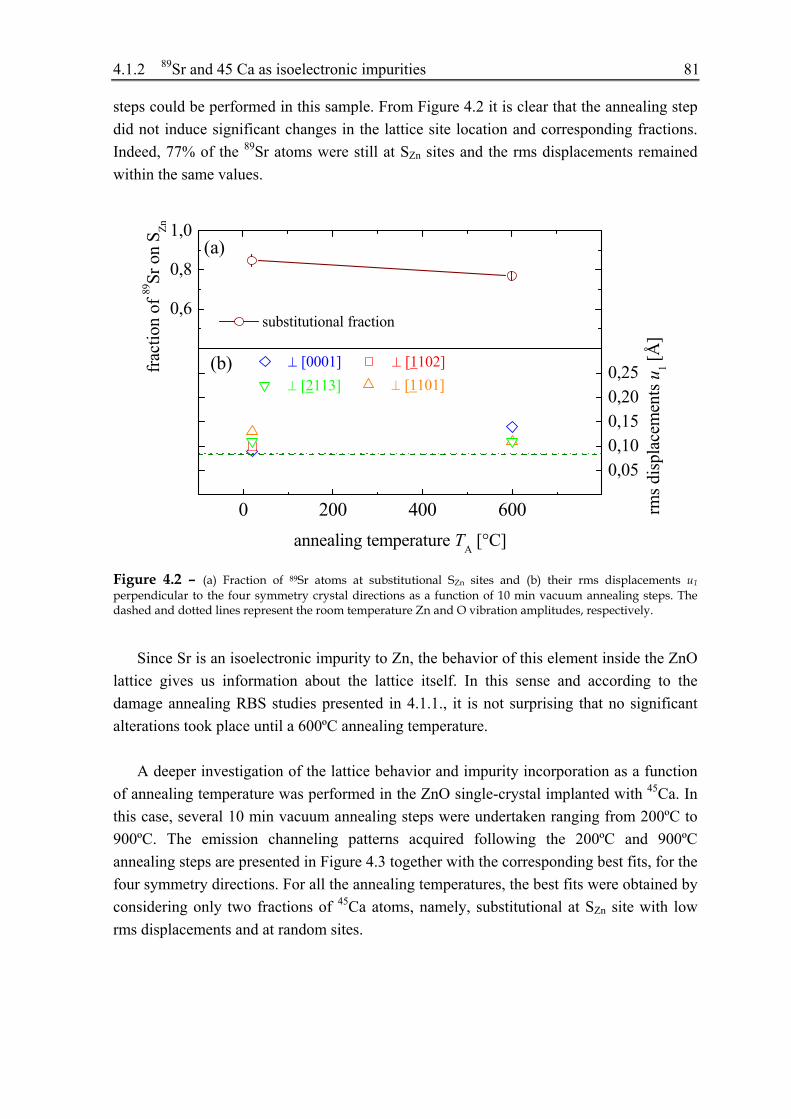
4.1.2 89Sr and 45 Ca as isoelectronic impurities 81
steps could be performed in this sample. From Figure 4.2 it is clear that the annealing step did not induce significant changes in the lattice site location and corresponding fractions. Indeed, 77% of the 89Sr atoms were still at SZn sites and the rms displacements remained within the same values.
0,6
0,8
1,0
substitutional fraction
(a)
fract
ion
of 89
Sr o
n S Zn
0 200 400 600
0,050,100,150,200,25 ⊥ [1102]
⊥ [1101] ⊥ [2113](b)
annealing temperature TA [°C]
rms d
ispla
cem
ents
u 1 [Å]
⊥ [0001]
Figure 4.2 – (a) Fraction of 89Sr atoms at substitutional SZn sites and (b) their rms displacements u1 perpendicular to the four symmetry crystal directions as a function of 10 min vacuum annealing steps. The dashed and dotted lines represent the room temperature Zn and O vibration amplitudes, respectively.
Since Sr is an isoelectronic impurity to Zn, the behavior of this element inside the ZnO lattice gives us information about the lattice itself. In this sense and according to the damage annealing RBS studies presented in 4.1.1., it is not surprising that no significant alterations took place until a 600ºC annealing temperature.
A deeper investigation of the lattice behavior and impurity incorporation as a function
of annealing temperature was performed in the ZnO single-crystal implanted with 45Ca. In this case, several 10 min vacuum annealing steps were undertaken ranging from 200ºC to 900ºC. The emission channeling patterns acquired following the 200ºC and 900ºC annealing steps are presented in Figure 4.3 together with the corresponding best fits, for the four symmetry directions. For all the annealing temperatures, the best fits were obtained by considering only two fractions of 45Ca atoms, namely, substitutional at SZn site with low rms displacements and at random sites.

82 4.1. Implantation damage annealing
Figure 4.3 – β- emission channeling patterns from 45Ca implanted on a ZnO single-crystal around the four symmetry directions [0001], [1102], [1101] and [2113] (patterns (a) - (d)), following the A) 200ºC and the B) 900ºC 10 min vacuum annealing steps. The corresponding theoretical patterns that best fitted the experimental ones are also presented (patterns (e) - (h)).
The emission channeling patterns after the 200ºC annealing are basically the same as the ones obtained for the as-implanted state. At this stage approximately 100% of the 45Ca atoms were placed at substitutional SZn site with rms displacements perpendicular to the symmetry directions of 0.17 Å, 0.12 Å, 0.12 Å and 0.11 Å. As expected, at this annealing temperature the rms displacements are higher than the Zn and O atoms thermal vibrations (0.082 Å and 0.085 Å, respectively). This indicates that there is still some degree of implantation damage that makes difficult the proper incorporation of Ca at substitutional Zn sites.
Inspection of the rms displacements behavior as a function of annealing temperature (Figure 4.4 (b)) reveals that this lattice site location proved to be quite stable until the 600ºC annealing temperature. Indeed, though the 45Ca fractions at SZn site suffered no considerable variations with the entire annealing procedure, the rms displacements from ideal Zn site started to decrease in a consistent manner with the 700ºC annealing. The best scenario was observed after 800ºC where for some of the directions u1 reached values
-2
-1
0
1
2
-2 -1 0 1 2(a)
(0110)
experiment-2 -1 0 1 2
1.12 -- 1.16 1.09 -- 1.12 1.05 -- 1.09 1.01 -- 1.05 0.97 -- 1.01 0.93 -- 0.97 0.89 -- 0.93 0.86 -- 0.89
simulation for SZn sites
(e) ([0001])
-2
-1
0
1
2
(1011)
(b)
(1120)
1.16 -- 1.20 1.12 -- 1.16 1.07 -- 1.12 1.03 -- 1.07 0.98 -- 1.03 0.94 -- 0.98 0.90 -- 0.94 0.86 -- 0.90
(f) ([1102])
-2
-1
0
1
2(2021)
(c)
(1120)
(d)
1.12 -- 1.16 1.09 -- 1.12 1.05 -- 1.09 1.01 -- 1.05 0.97 -- 1.01 0.93 -- 0.97 0.89 -- 0.93 0.86 -- 0.89
(g) ([1101])
[deg]-2 -1 0 1 2
-2
-1
0
1
2
(0110)
(1120)
-2 -1 0 1 2
(h) ([2113])
1.13 -- 1.16 1.10 -- 1.13 1.06 -- 1.10 1.03 -- 1.06 0.99 -- 1.03 0.96 -- 0.99 0.93 -- 0.96 0.90 -- 0.93
-2
-1
0
1
2
-2 -1 0 1 2(a)
(0110)
experiment-2 -1 0 1 2
1.20 -- 1.25 1.15 -- 1.20 1.10 -- 1.15 1.06 -- 1.10 1.01 -- 1.06 0.95 -- 1.01 0.90 -- 0.95 0.86 -- 0.90
simulation for SZn sites
(e) [0001]
-2
-1
0
1
2
(1011)
(b)
(1120)
1.20 -- 1.25 1.15 -- 1.20 1.10 -- 1.15 1.06 -- 1.10 1.01 -- 1.06 0.95 -- 1.01 0.90 -- 0.95 0.86 -- 0.90
(f) [1102]
-2
-1
0
1
2(c)
(2021)
(1120)
(d)
1.20 -- 1.25 1.15 -- 1.20 1.10 -- 1.15 1.06 -- 1.10 1.01 -- 1.06 0.95 -- 1.01 0.90 -- 0.95 0.86 -- 0.90
(g) [1101]
[deg]-2 -1 0 1 2
-2
-1
0
1
2
(0110)
(1120)
-2 -1 0 1 2
(h) [2113] 1.20 -- 1.25 1.15 -- 1.20 1.10 -- 1.15 1.06 -- 1.10 1.01 -- 1.06 0.95 -- 1.01 0.90 -- 0.95 0.86 -- 0.90
TA = 200ºC A)
TA = 900ºC B)

4.1.2 89Sr and 45 Ca as isoelectronic impurities 83
below the Zn and O thermal vibrations. This point towards a significant implantation damage annealing at 800ºC, with subsequent lattice recovery and, thus, better incorporation of Ca at SZn sites. This level of lattice recovery remained generally unchanged with the 900ºC annealing temperature.
Figure 4.4 – (a) Fraction of 45Ca atoms at substitutional SZn sites and (b) their rms displacements u1 perpendicular to the four symmetry crystal directions as a function of 10 min vacuum annealing steps. The dashed and dotted lines represent the room temperature Zn and O vibration amplitudes, respectively.
In spite that the damage annealing after an 800ºC annealing temperature was not investigated by RBS, from the EC results here presented there are evidences that the ZnO lattice would be considerably recovered already at 800ºC. These experiments reinforce the conclusions that the implantation damage can be eliminated with air or vacuum annealings at temperatures above 800ºC. It is also believed that the optimum lattice recovery is achieved at 1050ºC, though there are no EC results at this temperature due to experimental restrictions (the maximum annealing temperature in the EC setup is 900ºC).
Conclusions As isoelectronic impurities to Zn, the lattice site location of the ion implanted Sr and Ca elements can bring important information regarding the ZnO lattice recovery from the implantation damage. From the EC experiments it was possible to assign approximately 84% of the 89Sr atoms to the SZn site with low rms displacements (0.09 – 0.13 Å) perpendicular to the four symmetry directions. This scenario did not change considerably with the only annealing step performed in this sample at 600ºC, indicating that no significant lattice recovery took place at this annealing temperature.
A more thorough investigation was carried out in the single-crystal implanted with 45Ca. In the as-implanted state already ~100% of the Ca atoms were found at SZn with low
0,8
1,0
1,2
substitutional fraction
(a)
fract
ion
of 45
Ca o
n S Zn
0 200 400 600 800
0,050,100,150,200,25
⊥ [1102] ⊥ [1101] ⊥ [2113]
(b)
annealing temperature TA [°C]
rms d
ispla
cem
ents
u 1 [Å]
⊥ [0001]

84 4.2. Ion implanted p-type dopants in ZnO
rms displacements ranging from 0.11 Å to 0.17 Å. This scenario remained practically unchanged until a 700ºC vacuum annealing. With the 800ºC and 900ºC annealing steps the rms displacements decreased to values as low as the thermal vibration of the Zn and O atoms in the lattice. This indicates a better incorporation of the impurity at the Zn site and thus a lattice recovery from the implantation damage. It is also important to refer that throughout the entire annealing process the substitutional fraction of Ca at Zn site did not significantly vary.
In resume, the lattice site location studies of 89Sr and 45Ca ion implanted isotopes into single-crystalline ZnO revealed that the implantation damage decreases considerably for annealing temperature at or above 800ºC. This is in close agreement with the RBS studies performed on a ZnO single-crystal implanted with stable Fe (section 4.1.1), in spite of the different implantation doses (1016 at/cm2 of Fe Vs 1013 at/cm2 of Ca and Sr).
4.2. Ion implanted p-type dopants in ZnO As described in Chapter 1, p-type doping of ZnO is one of the most interesting topics
being studied nowadays in this II-VI semiconductor. In spite of the few successful cases of p-type doping of this intrinsically n-type semiconductor [2-9], there are still many questions without a clear answer. The group-I and group-V elements are among the most attractive p-type dopants for ZnO, if incorporated in substitutional Zn and O sites, respectively. However, group-I elements, particularly Li and Na, tend to form self-compensating interstitials while the group-V elements tend to sit at anti-sites acting therefore as donors instead of acceptors [10]. The mechanisms behind the behavior of these p-type dopants are still not well understood (refer to Chapter 1 for further information).
In this section the author presents and discusses this problematic for the group-Ib elements Cu and Ag. In what concerns the group-V dopants, As was selected as an interesting element to study. Still within the scope of the p-type doping, the author will address and try to bring further knowledge into one of the most promising p-type doping methods proposed by theory: the co-doping method [11-14]. According to this procedure, successful and efficient p-type doping of ZnO can be attained by introducing simultaneously a donor and an acceptor. In this section, the results obtained for the co-doping of ZnO with In and As will be discussed.
Following ion-implantation, the dopant lattice site location and local environment were evaluated as a function of annealing temperature by means of Emission Channeling (EC) and γ-γ Perturbed Angular Correlations (PAC).

4.2.1 Group Ib elements – Cu and Ag 85
4.2.1 Group Ib elements – Cu and Ag
4.2.1.1 67Cu implanted in ZnO
Besides being a potential p-type dopant of ZnO, a few other issues make of Cu an interesting element to study. The most widespread is its possible responsibility in the famous “structured” green band in ZnO [15] and, more recently, its successful role as a co-dopant in the activation of room temperature ferromagnetism in Zn0.94Fe0.05Cu0.01O [16] (see also Chapter 1). To better understand these mechanisms, a deeper knowledge of the Cu lattice site location in ZnO is envisaged.
In what follows, the author presents and discusses the results obtained following EC experiments with the aim of identifying the lattice site location of implanted Cu in single-crystalline ZnO. As usual, this study was carried out as a function of annealing temperature. Experimental details In this study a commercially available [0001] ZnO single-crystal was implanted at CERN/ISOLDE, at room-temperature, with 2.3×10¹³ at/cm2 of 67Cu (t1/2 = 61.9 h, see Figure A.3) with 60 keV energy (sample ZnO #175 on table 3.1). This corresponds to a maximum 67Cu concentration of 8×10¹⁸ at/cm3 (~96 ppm) at a depth of 259(116) Å. The angular distribution of the β- particles emitted in the 67Cu → 67Zn radioactive decay was measured with a position-sensitive detector along the [0001], [1102], [1101] and [2113] symmetry directions, according to the procedure described in section 2.3.5.. The emission channeling patterns were acquired for the as-implanted state and following 10 min in-situ vacuum annealing steps at 200ºC, 400ºC, 600ºC, 700ºC and 800ºC (see table 3.4).
The 67Cu lattice site locations were determined by comparing the experimental emission patterns with theoretical ones, according to the χ2 minimization method outlined in section 2.3.5. Several sites were tested in the fitting procedure, namely, 67Cu at substitutional Zn sites (SZn) with varying root mean square (rms) displacement u1, substitutional O sites and a wide range of interstitial sites (Figure 2.13 in Chapter 2). As usual, the Manybeam formalism (section 2.3.3) was used to calculate the 67Cu theoretical emission patterns. In this case, a energy range of 100-550 keV was considered in steps of 25 keV. The results were furthermore averaged according to the 67Cu β- spectrum. Results and discussion The experimental patterns for the four directions measured following the 200ºC and 600ºC annealing steps are depicted on Figure 4.7 A) and B), respectively, along with the corresponding best fits.

86 4.2. Ion implanted p-type dopants in ZnO
Figure 4.7 – β- emission channeling patterns from 67Cu implanted on a ZnO single-crystal around the four symmetry directions [0001], [1102], [1101] and [2113] (patterns (a) - (d)), following the A) 200ºC and the B) 600ºC 10 min vacuum annealing steps. The corresponding theoretical patterns that best fitted the experimental ones are also presented (patterns (e) - (h)).
The best fits were obtained considering only two fractions for all the directions and annealing temperatures. The channeling patterns for the 200ºC annealing are essentially the same as in the as-implanted state, with ~70% of the 67Cu atoms occupying substitutional SZn sites with rms displacements perpendicular to the directions [0001], [1102], [1101] and [2113] of 0.17 Å, 0.16 Å, 0.16 Å and 0.15 Å, respectively. These values are nearly twice the rms displacements of Zn and O atoms in the ZnO lattice (~0.08 Å) [17], but they are similar to the ones determined for 167mEr implanted in ZnO, though following a higher annealing temperature of 700ºC (see section 4.3.1.). The remaining 30% of the Cu atoms are believed to be located at the so called random sites, which result in an isotropic emission yield. There were no indications of Cu atoms at other well-defined lattice site positions, including interstitial sites.
The patterns acquired following the 600ºC annealing step (Figure 4.7 b) present some differences compared to the as-implanted state or the 200ºC emission patterns. More precisely, a general anisotropy reduction of roughly a factor of two was observed and the
-2
-1
0
1
2
-2 -1 0 1 2(a)
(0110)
experiment-2 -1 0 1 2
1.26 - 1.33 1.19 - 1.26 1.12 - 1.19 1.06 - 1.12 0.99 - 1.06 0.92 - 0.99 0.85 - 0.92 0.78 - 0.85
simulation for SZn sites
(e) [0001]
-2
-1
0
1
2
(1011)
(b)
(1120)
1.57 - 1.68 1.47 - 1.57 1.37 - 1.47 1.26 - 1.37 1.15 - 1.26 1.05 - 1.15 0.95 - 1.05 0.84 - 0.95
(f) [1102]
-2
-1
0
1
2(c)
(2021)
(1120)
(d)
1.50 - 1.59 1.40 - 1.50 1.31 - 1.40 1.22 - 1.31 1.12 - 1.22 1.03 - 1.12 0.93 - 1.03 0.84 - 0.93
(g) [1101]
[deg]-2 -1 0 1 2
-2
-1
0
1
2
(0110)
(1120)
-2 -1 0 1 2
(h) [2113] 1.38 - 1.46 1.31 - 1.38 1.23 - 1.31 1.15 - 1.23 1.07 - 1.15 1.00 - 1.07 0.92 - 1.00 0.84 - 0.92
-2
-1
0
1
2
-2 -1 0 1 2(a)
(0110)
experiment-2 -1 0 1 2
1.12 - 1.15 1.09 - 1.12 1.06 - 1.09 1.02 - 1.06 0.99 - 1.02 0.96 - 0.99 0.93 - 0.96 0.90 - 0.93
simulation displaced SZn sites
(e) [0001]
-2
-1
0
1
2
(1011)
(b)
(1120)
1.25 - 1.30 1.19 - 1.25 1.14 - 1.19 1.09 - 1.14 1.04 - 1.09 0.99 - 1.04 0.93 - 0.99 0.88 - 0.93
(f) [1102]
-2
-1
0
1
2
(c)
(2021)
(1120)
(d)
1.24 - 1.29 1.18 - 1.24 1.13 - 1.18 1.08 - 1.13 1.03 - 1.08 0.98 - 1.03 0.92 - 0.98 0.87 - 0.92
(g) [1101]
[deg]-2 -1 0 1 2
-2
-1
0
1
2
(0110)
(1120)
-2 -1 0 1 2
(h) [2113] 1.13 - 1.17 1.10 - 1.13 1.06 - 1.10 1.02 - 1.06 0.99 - 1.02 0.95 - 0.99 0.92 - 0.95 0.88 - 0.92
TA = 200ºC A)
TA = 600ºC B)

4.2.1 Group Ib elements – Cu and Ag 87
relative intensity of the axial effects diminished considerably with respect to the planar channeling effects. Notice that, along the [0001] direction, there is a local minimum that was not observed for the previous annealing temperatures. These modifications suggested a change of the Cu lattice site location, which was confirmed by the fitting procedure. Indeed, after the 600ºC annealing step, ~95% of the Cu atoms were located at SZn site with large rms displacements of 0.42 Å, 0.44 Å, 0.44 Å and 0.46 Å. These large values point towards static displacements along specific crystal directions. For this reason, other sites were tested to fit the data, namely, sites that are shifted along the c-axis or along the basal bonding and anti-bonding directions. Nevertheless, the best fits were obtained for isotropic Gaussian distributions around SZn sites and it was not possible to relate the rms displacements from this site with specific directions.
From Figure 4.8 (a) it is clear that the fractions of Cu atoms at SZn sites remained unchanged up to the 400ºC annealing (~65%-70%). However, at this annealing temperature, u1 increased already to values between 0.22 Å and 0.26 Å (Figure 4.8 (b)).
Figure 4.8 – (a) Fraction of 67Cu atoms substitutional at SZn sites and (b) their room temperature rms displacements u1 perpendicular to the indicated crystal directions as a function of 10 min vacuum annealing steps. The dashed and dotted lines represent the room temperature rms displacements of Zn and O atoms.
As referred earlier, the 600ºC annealing step induced a further increase of the rms displacements as well as of the substitutional fraction of Cu. While u1 remained within the same range of values (0.42 Å - 0.52 Å) following the 700ºC and 800ºC annealing steps, the fraction of Cu atoms at SZn decreased considerably to as low as 40%.
At this point it is important to point out that on dismounting the sample a few percent of the 67Cu activity was found inside the EC measurement vacuum chamber, which indicates that Cu out-diffusion occurred during the annealings. Ref. [18] suggests a diffusion coefficient for Cu in ZnO of D = 2×10⁷ exp(-4.8 eV/kT) cm2/s. This yields a diffusion width of approximately 60 Å for the 10 min 800ºC annealing. Though this value

88 4.2. Ion implanted p-type dopants in ZnO
is comparable to the implantation depth of 259 Å, the fact is that the changes in the lattice site configuration of Cu were observed already at 400ºC, being more pronounced after the 600ºC annealing. It becomes important to comment on the possible effects of this diffusion in the fitted Cu fractions. Indeed, they are quite sensitive to the Cu depth profile, since the emission channeling effects decrease with increasing depth of the emitter atoms from the surface due to dechanneling of the particles. Since the simulations used to fit all annealing temperature data were based on an unchanged Cu as-implanted profile, which must have obviously changed by the subsequent Cu diffusion, the fitted fractions of Cu at SZn site were marked in Figure 4.8 (a) as being less accurate for annealing temperatures at and above 600ºC. In this sense, it is possible that the increase of the near substitutional Cu fraction at 600ºC and the reduction following the 700ºC and 800ºC annealing are simply reflecting changes in the Cu depth profile. This same interpretation is not applicable to the Cu rms displacements. Indeed, by fitting the experimental patterns with simulations resulting from a constant 67Cu depth profile from 0 to 5000Å, it was possible to infer that the Cu rms displacements would still be around 0.42-0.52 Å. This means that the Cu rms displacements from the ideal SZn site do not depend significantly on the Cu depth profile.
Conclusions The findings here presented seem to be in close agreement to the PL experiments mentioned in Chapter 1, where the characteristic ZnO green band was attributed to other defects not involving Cu [19]. Indeed, in spite of the limitations above described, the EC results suggest that annealing at 800ºC induces a considerable reduction of the fraction of Cu atoms located at substitutional Zn sites (~ 40%). Moreover, the Cu rms displacements from ideal SZn are quite large and, as argued above, these values are pretty much reliable. Since the PL experiments presented in Ref. [19] were performed following an 800ºC annealing, and in spite that oxygen was used as annealing atmosphere, the results here presented reinforce the hypothesis that the green band is not related with Cu atoms at Zn site.
Moreover, they further suggest that the non-incorporation of Cu at SZn site should not be pointed out as the main reason for the non-achievement of p-type doped ZnO with this group-Ib element. Indeed, 70% - 95% of the Cu atoms were found at almost ideal SZn sites up to a 600ºC annealing temperature. Therefore, most probably the presence of compensating defects, intrinsic or not, are the main responsible for the p-type doping problematic with this element. This same statement is not true for higher annealing temperatures since a considerable reduction of the Cu substitutional fraction at Zn site was observed.
4.2.1.2 111Ag implanted in ZnO
As a Ib element, Ag is one of the potential acceptors in ZnO if incorporated on substitutional defect-free Zn (SZn) sites. Nevertheless, previous studies, where Ag-doped ZnO was investigated with respect to its application in varistors, suggested that Ag acts as

4.2.1 Group Ib elements – Cu and Ag 89
an amphoteric dopant, existing both on substitutional Zn sites and in the interstitial form [20]. The behavior of this element implanted in ZnO was investigated by means of the EC and PAC techniques. More precisely, EC gave evidence of the Ag lattice site location, while structural disturbances, such as, dislocations and specific defects located in the Ag atoms neighborhood were monitored by means of Perturbed γ-γ Angular Correlations (PAC). In both cases the 111Ag isotope was used to perform the studies.
Emission channeling experiments Experimental details To address the lattice site location of Ag in ZnO, a commercially available [0001] single-crystal of this II-VI semiconductor was implanted at CERN/ISOLDE with 2×10¹³ at/cm2 of the radioactive isotope 111Ag (t1/2 = 7.45 d, β- decay) with an energy of 60 keV (Sample E-Z3 on table 3.1). With these implantation parameters, the projected range and straggling of the Ag atoms are 185 Å and 72 Å, respectively.
The angular distributions of the β- particles emitted from the 111Ag → 111Cd decay (Figure A.4 in Appendix A) were measured by means of a position sensitive detector in the as-implanted state and following each of the 10 min vacuum annealing steps at 200ºC, 400ºC, 600ºC and 800ºC (see table 3.4). As usual, the measurements were carried out along the four symmetry directions [0001], [1102], [1101] and [2113]. For extraction of the emission channeling patterns, an energy window was set from 25 keV up to the β- endpoint energy of 1.03 MeV. In the fitting procedure (outlined in section 2.3.5.), to evaluate the Ag lattice site location, the considered theoretical lattice sites were substitutional Zn sites (SZn) and substitutional O sites (SO) with varying Gaussian root mean square (rms) displacements, as well as several interstitial sites (Figure 2.13 in Chapter 2).
Results and discussion The best fits for the as-implanted state (Figure 4.9 (A)) were obtained by considering only two fractions of Ag atoms, namely, ~30% substitutional at SZn and ~70% at random sites. The best-fit values of the Ag rms displacements from ideal SZn sites were 0.18, 0.17, 0.20 and 0.26 Å perpendicular to the [0001], [1102], [1101] and [2113] directions, respectively, which is larger than the thermal vibration amplitude of the Zn atoms of u1(Zn)=0.082 Å. Moreover, these rms displacement values are similar to the ones obtained for the as-implanted state of 67Cu, another group Ib element that could act as an acceptor in ZnO, as presented on the previous section of this dissertation. Nevertheless, the fraction of Cu atoms at Zn sites was considerably higher (~70%).

90 4.2. Ion implanted p-type dopants in ZnO
Figure 4.9 – Angular distributions of the β- particles emitted from 111Ag in ZnO around the four symmetry directions [0001], [1102], [1101] and [2113] (patterns (a) - (d)), for the A) as-implanted state and B) following the a 600ºC 10 min vacuum annealing. The corresponding theoretical patterns that best fitted the experimental ones are also presented (patterns (e) - (h)).
The 600ºC 10 min vacuum annealing induced a degradation of the channeling effects,
as can be inferred from the emission patterns presented in Figure 4.9 (B). More precisely, not only a considerable decrease of the overall anisotropy of the channeling patterns was observed, but also the relative intensities of the planar and axial effects changed, suggesting that the Ag lattice sites altered. Indeed, the best fits for these patterns indicate that approximately 46% of the Ag atoms are located at SZn, but with high rms displacements of the order of 0.38 – 0.52 Å.
A better visualization of the behavior of the Ag fraction at SZn site and of the corresponding rms displacements as a function of the annealing temperature is attained from Figure 4.10 (a) and (b), respectively.
-1
0
1
2
-1 0 1 2 3(a)
(0110)
experiment-1 0 1 2 3
1.17 - 1.20 1.13 - 1.17 1.10 - 1.13 1.07 - 1.10 1.03 - 1.07 1.00 - 1.03 0.96 - 1.00 0.93 - 0.96
simulation for SZn sites
(e) [0001]
-2
-1
0
1
2
(1011)
(b)
(1120)
1.31 - 1.36 1.25 - 1.31 1.20 - 1.25 1.14 - 1.20 1.09 - 1.14 1.04 - 1.09 0.98 - 1.04 0.93 - 0.98
(f) [1102]
-2
-1
0
1
2(c)
(2021)
(1120)
(d)
1.21 - 1.25 1.17 - 1.21 1.13 - 1.17 1.09 - 1.13 1.05 - 1.09 1.01 - 1.05 0.97 - 1.01 0.93 - 0.97
(g) [1101]
[deg]-2 -1 0 1 2
-1
0
1
2
3
(0110)
(1120)
-2 -1 0 1 2
(h) [2113] 1.11 - 1.14 1.09 - 1.11 1.06 - 1.09 1.03 - 1.06 1.01 - 1.03 0.98 - 1.01 0.96 - 0.98 0.93 - 0.96
-2
-1
0
1
2-2 -1 0 1 2
(a)
(0110)
experiment-2 -1 0 1 2
1.09 - 1.11 1.07 - 1.09 1.05 - 1.07 1.03 - 1.05 1.01 - 1.03 0.99 - 1.01 0.97 - 0.99 0.95 - 0.97
simulation for near-SZn sites
(e) [0001]
-2
-1
0
1
2
(1011)
(b)
(1120)
1.17 - 1.20 1.13 - 1.17 1.10 - 1.13 1.07 - 1.10 1.03 - 1.07 1.00 - 1.03 0.96 - 1.00 0.93 - 0.96
(f) [1102]
-2
-1
0
1
2(c)
(2021)
(1120)
(d)
1.15 - 1.18 1.12 - 1.15 1.09 - 1.12 1.06 - 1.09 1.03 - 1.06 1.00 - 1.03 0.97 - 1.00 0.94 - 0.97
(g) [1101]
[deg]-2 -1 0 1 2
-2
-1
0
1
2
(0110)
(1120)
-2 -1 0 1 2
(h) [2113] 1.06 - 1.08 1.04 - 1.06 1.02 - 1.04 1.00 - 1.02 0.99 - 1.00 0.97 - 0.99 0.95 - 0.97 0.93 - 0.95
As-Implanted A)
TA = 600ºC B)

4.2.1 Group Ib elements – Cu and Ag 91
0,20,40,60,81,0
Ag diffusion⇒ fractions less accurate
(a)fra
ctio
n of
111 A
g on
SZn
0 200 400 600 800
0,10,20,30,40,50,6
⊥ [1101]⊥ [2113]
⊥ [1102](b)
annealing temperature TA [°C]
rms d
ispla
cem
ents
u 1 [Å]
⊥ [0001]
Figure 4.10 – (a) Fraction of 111Ag atoms at SZn sites and (b) their rms displacements u1 perpendicular to the four symmetry crystal directions as a function of 10 min vacuum annealing steps. The dashed and dotted lines represent the room temperature Zn and O vibration amplitudes, respectively.
A progressive increase of the substitutional Ag fraction at SZn was observed up to the
600ºC annealing step, reaching the maximum value of 46% for this temperature, as referred previously. Nevertheless, the rms displacements from the ideal SZn site, perpendicular to the symmetry directions, experienced also a considerable increase, changing from around 0.23-0.32 Å (400ºC annealing) to 0.38-0.52 Å. These rms displacements are not only unusually large but also they vary considerably perpendicular to the four symmetry directions, pointing out to displacements along particular crystal directions. This same behavior was observed for 67Cu implanted in ZnO, presented earlier, and in a similar way, other sites were tested to fit the data. More precisely, it was explored the possibility that the Ag atoms were displaced towards the bond-centre (BC) or anti-bonding (AB) positions within the c-axis or towards the three BC or AB positions that are off the c-axis (Figure 2.12 in Chapter 2). Though a fixed displacement of 0.3 – 0.5 Å from SZn to the off c-axis BC positions yielded a good fit quality, this was still worse than the χ2 resulting from the isotropic Gaussian rms displacements given above.
Around 30% of the Ag atoms out-diffused following the 800ºC annealing step, as was clear from the activity loss from the ZnO single-crystal. Nevertheless, the fraction at SZn of the remaining Ag atoms did not change considerably, as well as, the rms displacements, which stayed at high values. Similarly to the case of 67Cu implanted on ZnO, it is important to refer that the Ag diffusion obviously also affected its depth profile, which consequently may have influenced the fraction values obtained from the fitting procedure. This is related to the fact that the theoretical emission patterns were calculated assuming an as-implanted
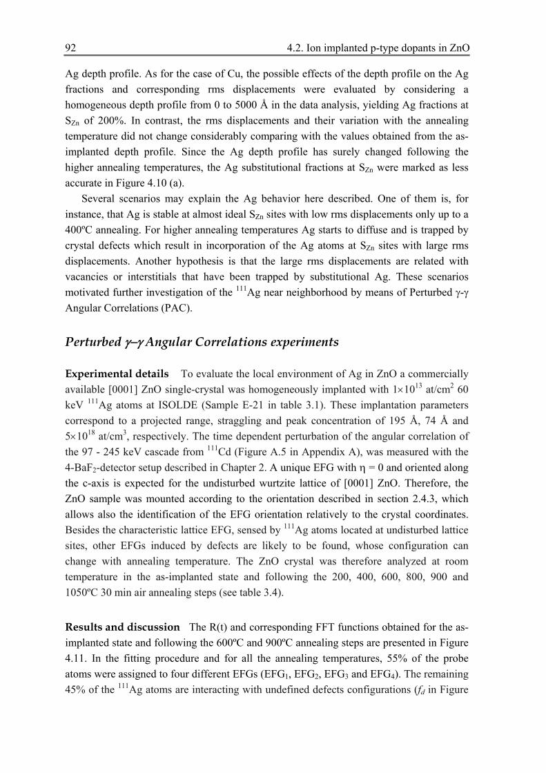
92 4.2. Ion implanted p-type dopants in ZnO
Ag depth profile. As for the case of Cu, the possible effects of the depth profile on the Ag fractions and corresponding rms displacements were evaluated by considering a homogeneous depth profile from 0 to 5000 Å in the data analysis, yielding Ag fractions at SZn of 200%. In contrast, the rms displacements and their variation with the annealing temperature did not change considerably comparing with the values obtained from the as-implanted depth profile. Since the Ag depth profile has surely changed following the higher annealing temperatures, the Ag substitutional fractions at SZn were marked as less accurate in Figure 4.10 (a).
Several scenarios may explain the Ag behavior here described. One of them is, for instance, that Ag is stable at almost ideal SZn sites with low rms displacements only up to a 400ºC annealing. For higher annealing temperatures Ag starts to diffuse and is trapped by crystal defects which result in incorporation of the Ag atoms at SZn sites with large rms displacements. Another hypothesis is that the large rms displacements are related with vacancies or interstitials that have been trapped by substitutional Ag. These scenarios motivated further investigation of the 111Ag near neighborhood by means of Perturbed γ-γ Angular Correlations (PAC).
Perturbed γ−γ Angular Correlations experiments Experimental details To evaluate the local environment of Ag in ZnO a commercially available [0001] ZnO single-crystal was homogeneously implanted with 1×10¹³ at/cm2 60 keV 111Ag atoms at ISOLDE (Sample E-21 in table 3.1). These implantation parameters correspond to a projected range, straggling and peak concentration of 195 Å, 74 Å and 5×10¹⁸ at/cm3, respectively. The time dependent perturbation of the angular correlation of the 97 - 245 keV cascade from 111Cd (Figure A.5 in Appendix A), was measured with the 4-BaF2-detector setup described in Chapter 2. A unique EFG with η = 0 and oriented along the c-axis is expected for the undisturbed wurtzite lattice of [0001] ZnO. Therefore, the ZnO sample was mounted according to the orientation described in section 2.4.3, which allows also the identification of the EFG orientation relatively to the crystal coordinates. Besides the characteristic lattice EFG, sensed by 111Ag atoms located at undisturbed lattice sites, other EFGs induced by defects are likely to be found, whose configuration can change with annealing temperature. The ZnO crystal was therefore analyzed at room temperature in the as-implanted state and following the 200, 400, 600, 800, 900 and 1050ºC 30 min air annealing steps (see table 3.4).
Results and discussion The R(t) and corresponding FFT functions obtained for the as-implanted state and following the 600ºC and 900ºC annealing steps are presented in Figure 4.11. In the fitting procedure and for all the annealing temperatures, 55% of the probe atoms were assigned to four different EFGs (EFG1, EFG2, EFG3 and EFG4). The remaining 45% of the 111Ag atoms are interacting with undefined defects configurations (fd in Figure
4.2.1 Group Ib elements – Cu and Ag 93
4.12 b)), which instigate a large EFG distribution that leads to an observed reduced amplitude of the R(t) function.
-0,04
-0,02
0,00
0,02
0,04
-0,04
-0,02
0,00
0,02
0,040
1
2
3
0
1
2
3
0 50 100 150 200 250 300 350 400
-0,04
-0,02
0,00
0,02
0,04
0 100 200 300 4000
1
2
3e)
d)c)
b)
R(t)
As-Implanted
R(t)
600ºC/air/30´
EFG3
EFG4EFG2
EFG1
F(W)
As-Implanted
EFG4
EFG3EFG2
EFG1
F(W)
600ºC/air/30'
f)
900ºC/air/30´
R(t)
Time (ns)
a)
EFG4
EFG3EFG2
EFG1
F(W)
W (Mrad/s)
900ºC/air/30'
Figure 4.11 – R(t) functions and FFT for the (a, b) as-implanted state and following the (c, d) 600ºC and (e, f) 900ºC air annealing steps. The best fitted functions are also depicted.
Through Figure 4.11 it is possible to evaluate for each EFG the temperature dependence of νQ, η, the 111Ag fractions (f) and the attenuation δ related with the distribution of EFGs. The results indicate that in the as-implanted state 42% of the 111Ag atoms were located at defect-free SZn sites, experiencing the lattice symmetry EFG1 characterized by νQ(1)~32 MHz, η(1) = 0 and oriented along the [0001] direction (θ = 0º and ϕ = 45º). In spite that at this point νQ(1) was still attenuated by δ1 ~ 11 %, with increasing annealing temperature this parameter decreased to the minimum value of 0.02 % (Figure 4.12 b)). This situation took place already after the 800ºC annealing suggesting a local lattice recovery. Moreover, f1 did not change considerably with the annealing procedure which, together with the values obtained for this fraction, is in close agreement with the EC results, presented earlier in this section, where 30% of the 111Ag atoms were found to be stably located at SZn sites.

94 4.2. Ion implanted p-type dopants in ZnO
20406080
100120140160180
νQ (3) νQ (4)
η
ν Q (M
Hz)
νQ (1) νQ (2)
0 200 400 600 800 10000,0
0,2
0,4
0,6
0,8
1,0
a)
η3 η4
TA (ºC)
η1 η2
01020304050
f 4 f d Undef. def. config.
δ(%)
f (%
) f1 f2 f3
0 200 400 600 800 10000
5
10
15
b)
TA (ºC)
δ1 δ2 δ3 δ4
Figure 4.12 – Annealing temperature dependence of a) νQ and η and b) of the 111Ag fractions f and attenuation δ. Above 900ºC, the quoted fractions were equally normalized to account for 23% of 111Ag out-diffusion, except for f5, as from this fraction only 7% out-diffused.

4.2.1 Group Ib elements – Cu and Ag 95
As referred previously, the results evidenced the presence of three more EFGs with high η and fractions ranging from 3% to 13%, which were assigned to defects. These fractions proved to be quite stable throughout the annealing process, but no EFG orientation could be inferred from the fitting procedure. Notice that while the asymmetry parameter η remained high with the annealings, the attenuation δ had a general tendency to decrease (Figure 4.12).
One of the most interesting aspects of the analysis lays in the EFG2 parameters following the 200ºC and 400ºC annealings. Indeed, the νQ(2)~32 MHz, close to the νQ(1) value, and the large η2 ~ 0.53-0.61, suggests the presence of 111Ag atoms at SZn site seeing a specific defect. Up to the 400ºC annealing, EFG3 and EFG4 are characterized by νQ(3)~117 MHz and νQ(4)~162 MHz. However, the configuration of the three defects was altered by the 600ºC annealing, as can be inferred from the new values found for the coupling constants νQ(2) ~ 52 MHz, νQ(3) ~ 134 MHz and νQ(4) ~ 182 MHz. Furthermore, the EFG2 disappearance following the 1050ºC annealing and the simultaneous f1 increase point out that the 111Ag atoms formerly associated to EFG2 were incorporated in defect-free SZn lattice sites. In contrast, EFG3 and EFG4 have resisted to this final annealing step, suggesting the inherent difficulty to completely eliminate local defect configurations associated to implanted Ag in ZnO.
Approximately 30% of the Ag atoms out-diffused with the 900ºC annealing. One would be tempted to conclude that the lost 111Ag atoms were the ones in undefined defect configurations (fd), since they could more easily escape from the crystal. This hypothesis can be evaluated by comparing the observable effective amplitude of the R(t) functions for the 800ºC and 900ºC annealing steps. If this value increased, the above referred assumption is confirmed. In fact, such an increase took place, but only by 7 %. This means that from the 30% Ag atoms that out-diffused, only 7% belonged to fraction fd (undefined defects configuration). Therefore, the remaining 23% came from the other 111Ag fractions (defect-free SZn sites + 3 defect configurations). From the experimental data and fitting procedure it was not possible to assign univocally these 23% to a specific fraction, for which in Figure 4.12 b) the quoted fractions above 900ºC were equally normalized to account for this loss. Nevertheless, it is important to mention that the higher temperature annealing at 1050ºC did not induce further 111Ag out-diffusion which is a strong indicator that at 900ºC only those atoms in a specific lattice/defect configuration, with well-defined activation energy, have escaped.
Conclusions
From the EC and PAC results important conclusions can be inferred. First of all, a small percentage (30% - 45%) of the Ag atoms was found to be located at defect-free SZn sites and this fraction did not change significantly with the annealing procedure. Moreover, three highly stable defects associated to Ag implanted in single-crystalline ZnO were

96 4.2. Ion implanted p-type dopants in ZnO
detected in small fractions ranging from 3% to 13%. Both techniques revealed that 600ºC is a key annealing temperature in terms of modification of these defects configuration, though they were still present after the high temperature annealing at 1050ºC. Out-diffusion of Ag starts already at 800ºC.
The findings here described strongly suggest that the difficulty in achieving p-type doped ZnO by means of the Ib dopant Ag is related with the low percentage of Ag atoms substitutional at defect-free SZn sites together with the association of this element with highly stable defects that might act as compensating mechanisms. Moreover, the amphoteric behavior of Ag suggested by other authors [20] was not confirmed by the experiments here presented, since no evidences were found for Ag at other regular, in particular, well-defined interstitial sites.
4.2.2. Group V elements - As
As referred earlier, As is one of the most promising p-type dopants for ZnO. In spite of the reported successful cases of As p-type doped ZnO [3-8], the mechanism behind it is not clear. The relevance of knowing the lattice site location of this group-V element is evident from what was exposed in Chapter 1. However, until now, no experimental method was able to provide reliable knowledge on the lattice site of As in ZnO, what has motivated the EC experiments with the 73As isotope here presented.
Experimental details The lattice site location of As in ZnO was investigated by means of the EC technique following implantation of a [0001] commercially available ZnO single-crystal with 60 keV 73As atoms up to a dose of 2×10¹³ at/cm2 (Sample E-O15 on table 3.1). These implantation parameters yield a projected range and straggling of 234 Å and 100 Å, respectively. The experimental procedure consisted of measuring the angular distribution of the 42.3 keV and 52.1 keV conversion electrons emitted from the 73As → 73Ge electron capture decay (t1/2 = 80.3 d, Figure A.5 in Appendix A) around the four symmetry directions of the crystal. These measurements were carried out for the as-implanted state and following 10 min in-situ vacuum annealing steps at 300ºC, 600ºC and 900ºC (see table 3.4). Since what is actually measured is the 73Ge lattice site location, due to the fact that 73As decays to an excited state of 73mGe (t1/2 = 2.95 μs) which subsequently decays to the ground state emitting the above referred conversion electrons, it is important to clarify a few points before moving forward. A nuclear recoil energy of only 0.54 eV is transferred to the 73Ge atom during the 73As decay, which is considerably smaller than the atomic displacement energy of 0.57 eV reported for ZnO [21]. This means that 73mGe inherits the 73As lattice site, same is to say, we are truly evaluating the 73As lattice site.
The lattice location of As was determined by comparing the experimental patterns with theoretical ones, according to the fitting procedure described in section 2.3.5. Several

4.2.2 Group V elements – As 97
theoretical emission patterns were considered to fit the data, namely, patterns resulting from the emitter at substitutional Zn (SZn) and O (SO) sites with varying rms displacements, the main interstitial sites and a diversity of interstitial sites with displacements along or basal to the c axis (see Figure 2.12 in Chapter 2).
Results and discussion In Figure 4.13 the experimental emission patterns obtained following the 300ºC and 900ºC annealing steps are depicted, together with the best fits, for each symmetry direction of the ZnO crystal.
Figure 4.13 – Angular distributions of conversion electrons from 73As in ZnO around the four symmetry directions [0001], [1102], [1101] and [2113] (patterns (a) - (d)), following the 10 min vacuum annealing steps at A) 300ºC and B) 900ºC. The corresponding theoretical patterns that best fitted the experimental ones are also presented (patterns (e) - (h)).
The best fits for the 300ºC annealing step (Figure 4.13 A)) were obtained by
considering only two fractions of As atoms, namely, substitutional at SZn site with low rms displacements and at random sites. As referred previously, the random sites either have very low crystal symmetry or are located in heavily damaged surroundings, contributing thus with an isotropic emission yield. In terms of the substitutional fractions, 94%, 83%, 98% and 91% of the As atoms were found at SZn site along the [0001], [1102], [1101] and
-2
-1
0
1
2
-2 -1 0 1 2(a)
(0110)
experiment-2 -1 0 1 2
1.10 - 1.14 1.05 - 1.10 1.01 - 1.05 0.97 - 1.01 0.92 - 0.97 0.88 - 0.92 0.83 - 0.88 0.79 - 0.83
simulation SZn sites
(e) [0001]
-2
-1
0
1
2
(1011)
(b)
(1120)
1.28 - 1.35 1.22 - 1.28 1.15 - 1.22 1.09 - 1.15 1.02 - 1.09 0.95 - 1.02 0.89 - 0.95 0.82 - 0.89
(f) [1102]
-1
0
1
2
3
(c)
(2021)
(1120)
(d)
1.21 - 1.27 1.16 - 1.21 1.10 - 1.16 1.04 - 1.10 0.99 - 1.04 0.93 - 0.99 0.88 - 0.93 0.82 - 0.88
(g) [1101]
[deg]-2 -1 0 1 2
-1
0
1
2
3
(0110)
(1120)
-2 -1 0 1 2
(h) [2113] 1.27 - 1.34 1.21 - 1.27 1.14 - 1.21 1.08 - 1.14 1.01 - 1.08 0.94 - 1.01 0.88 - 0.94 0.81 - 0.88
-2
-1
0
1
2-2 -1 0 1 2
(a)
(0110)
experiment-2 -1 0 1 2
1.08 - 1.11 1.04 - 1.08 1.00 - 1.04 0.97 - 1.00 0.94 - 0.97 0.90 - 0.94 0.87 - 0.90 0.83 - 0.87
simulation SZn +T sites
(e) [0001]
-2
-1
0
1
2
(1011)
(b)
(1120)
1.18 - 1.23 1.13 - 1.18 1.08 - 1.13 1.03 - 1.08 0.99 - 1.03 0.94 - 0.99 0.89 - 0.94 0.84 - 0.89
(f) [1102]
-2
-1
0
1
2
(c)
(2021)
(1120)
(d)
1.11 - 1.15 1.08 - 1.11 1.04 - 1.08 1.00 - 1.04 0.97 - 1.00 0.93 - 0.97 0.90 - 0.93 0.86 - 0.90
(g) [1101]
[deg]-2 -1 0 1 2-2
-1
0
1
2
(0110)
(1120)
-2 -1 0 1 2
(h) [2113] 1.12 - 1.15 1.08 - 1.12 1.05 - 1.08 1.01 - 1.05 0.98 - 1.01 0.95 - 0.98 0.91 - 0.95 0.88 - 0.91
TA = 300ºC A)
TA = 900ºC B)

98 4.2. Ion implanted p-type dopants in ZnO
[2113] directions, respectively, and the corresponding rms displacements perpendicular to these directions were 0.13 Å, 0.11 Å, 0.13 Å and 0.11 Å. Moreover, no evidence was found for As located at other lattice sites. The theoretical channeling patterns from emitter atoms on substitutional O sites (SO) and tetrahedral interstitial T sites were tested to fit the experimental data, but yielded inferior results. Indeed, a simple visualization of these theoretical patterns (Figure 4.14) reveals that they are clearly incompatible with the experimental ones (Figure 4.13 A)). All these facts lead to the conclusion that following the 300ºC annealing 90(8) % of the As atoms occupied substitutional SZn sites with rms displacements of 0.11-0.13 Å and the remaining emitter atoms were located at random sites.
-2 -1 0 1 2(a)
simulations for SO sites
1.25 - 1.31 1.18 - 1.25 1.12 - 1.18 1.05 - 1.12 0.99 - 1.05 0.93 - 0.99 0.86 - 0.93 0.80 - 0.86
-2 -1 0 1 2simulations for T sites
(d) [1102] 1.15 - 1.21 1.10 - 1.15 1.05 - 1.10 0.99 - 1.05 0.94 - 0.99 0.88 - 0.94 0.83 - 0.88 0.77 - 0.83
1.23 - 1.29 1.17 - 1.23 1.12 - 1.17 1.06 - 1.12 1.00 - 1.06 0.95 - 1.00 0.89 - 0.95 0.83 - 0.89
(b) 1.15 - 1.20 1.10 - 1.15 1.05 - 1.10 1.00 - 1.05 0.96 - 1.00 0.91 - 0.96 0.86 - 0.91 0.81 - 0.86
(e) [1101]
-2 -1 0 1 2
1.51 - 1.60 1.42 - 1.51 1.33 - 1.42 1.24 - 1.33 1.14 - 1.24 1.05 - 1.14 0.96 - 1.05 0.87 - 0.96
(c)
-2 -1 0 1 2
1.23 - 1.29 1.17 - 1.23 1.12 - 1.17 1.06 - 1.12 1.00 - 1.06 0.95 - 1.00 0.89 - 0.95 0.83 - 0.89
(f) [2113]
[deg] Figure 4.14 – Theoretical emission channelling patterns for 100% of emitter atoms located at substitutional SO sites (patterns (a)-(c)) and 100% on tetrahedral T sites (patterns (d)-(f). Notice that no patterns are depicted for [0001] because these sites cannot be distinguished along this direction (they are identical to the patterns for SZn).
Important alterations took place with the 900ºC annealing. The experimental emission patterns show that the As lattice site location has changed (Figure 4.13 B)). Indeed, an anisotropy decrease was observed along the four directions, much more pronounced for [1102], [1101] and [2113], suggesting that some fraction of the emitter atoms no longer occupied the SZn sites. The fit results confirmed this suspicion, since now only 83% of the As atoms were found at SZn along [0001]. The results are even more interesting for the other three directions, along which other sites can be distinguished. The introduction of an additional fraction of emitter atoms at or within a distance of 0.4 Å from interstitial T sites improved the χ2 fit for the [1102], [1101] and [2113] patterns by 13%, 12%, and 55%,

4.2.2 Group V elements – As 99
respectively. The best fits were thus obtained for 62(4) % of emitter atoms on substitutional Zn sites and 28(3) % at or close to interstitial T sites.
Figure 4.15 resumes the variation of the 73As fractions at SZn and T sites as a function of the annealing temperature. In the as-implanted state 73% of the emitter atoms were already found at SZn and there are evidences that a fraction of the remaining emitter atoms were located on interstitial sites out of the c-axis. However, from the results it was not possible to identify the specific interstitial site. While the 300ºC annealing maximized the 73As fraction at SZn, reaching the highest value of 90(8) %, a progressive decrease of this fraction was observed with the subsequent annealing steps at 600ºC and 900ºC, after which only 62(4) % of the emitter atoms were at SZn sites. The 73As fraction at T sites remained always quite low throughout the annealing procedure, except following the last annealing step. As referred above, at 900ºC ~30% of the emitter atoms were found at tetrahedral T sites. It is also important to mention that the rms displacements from ideal substitutional Zn sites were always in the range 0.07 – 0.17 Å, which is somewhat larger than the thermal vibration amplitude of the Zn atoms u1(Zn) = 0.080 Å.
0 100 200 300 400 500 600 700 800 9000.00.10.20.30.40.50.60.70.80.91.0
substitutional Zn sites SZn
interstitial T sites sum of SZn and T sites73
As f
ract
ion
annealing temperature [°C] Figure 4.15 – Fractions of 73As atoms at SZn and tetrahedral interstitial T sites as a function of 10 min vacuum annealing steps. The sum of both fractions is also shown.
Conclusions The most important conclusion that can be drawn from the results here presented is that the majority of implanted As atoms do not occupy substitutional O sites. As predicted by theory [10, 22], As acts as an “anti-site” impurity in ZnO. This result provides thus a clear proof that impurities in semiconductors may occupy sites which are different from what one would expect only from their chemical properties. This finding is particularly useful for understanding and modeling of new semiconductor properties, since it is very rare to find clearly reported cases in the literature of direct evidence of “anti-site” impurities. As suggested by Ref. [2], the As behavior can be explained by the considerable

100 4.2. Ion implanted p-type dopants in ZnO
mismatch between the ionic radii of As3- (2.22 Å) and O2- (1.38 Å) which results in a low solubility of As substituting for O in ZnO.
In terms of the mechanism behind the p-type character of As doped ZnO, the results here described contradict the idea that this type of conductivity is due to the formation of simple chemical AsO acceptors. In contrast, they are rather compatible with the complex model suggested by Ref. [22] that As would be located at SZn site surrounded by two Zn vancacies (AsZn -2VZn). The EC technique is not particularly sensitive to the direct surroundings of the probe atoms, for which the presence of VZn close to 73As would not be noticed unless it caused a significant displacement of the daughter nucleus 73mGe. From Ref. [22] two structures were proposed for this complex. If the complex is triply negatively charged, As should be 4-fold O-coordinated and remain relatively close to the ideal SZn position. On the other hand, in a neutral complex, As should be 5-fold O-coordinated and relax along the c axis, around 0.4-0.5 Å or halfway from the ideal Zn position towards the anti-bonding Zn site (AZ-c in Fig. 2.12 in Chapter 2). Although the AsZn-2VZn complexes should favorably form under O-rich growth conditions, it seems possible that they are also produced under O-poorer conditions, such as ion implantation and vacuum annealing in the case here presented. Since the EC results yielded low rms displacements of As atoms from the SZn site (0.07 -0.17 Å) one would be tempted to suggest that the correct structure for the As-2VZn complex is the first one proposed above (complex triply negatively charged). This would be true up to a 600ºC vacuum annealing. With the 900ºC annealing step a significant part of the As atoms moved to T sites, which could point out that the As-2VZn complex configuration changed to a neutral complex. However, the distance from the SZn to the T site is 1.6 Å, considerably larger than the relaxation predicted by Ref. [22]. Still, it is important to draw attention to the fact that the lattice location experiments take place when the 73As probe atoms have decayed to 73mGe, which can cause a change in the atomic structure of the complex, being thus slightly different from the one proposed by Ref. [22].
4.2.3 Co-doping with In and As In this section the author addresses the co-doping problematic in single-crystalline ZnO
co-implanted with In and As, according to the motivations exposed in Chapter 1. The EC and PAC techniques were used in this evaluation as they can provide relevant information about the dopant lattice sites and their local environments. It is important to point out that these are preliminary studies. To perform all the desirable and required experiments more beam time and “man power” are needed. Still, the findings that will be presented might well serve as guidelines for future experiments and studies within the scope of a PhD or Pos-Doc work.
The study starts with the analysis of 111In implanted in as-grown ZnO. The results of 73As implanted in ZnO were already described in section 4.2.2. These separate studies are

4.2.3 Co-doping with In and As 101
important as reference guides to the In + As co-doping experiments that will be presented in what follows.
4.2.3.1 111In implanted in ZnO
The lattice site location and local environment of 111In implanted in ZnO were
evaluated as a function of annealing temperature by means of the EC and PAC techniques.
Emission channeling experiments
Experimental details The 111In isotope was implanted on a [0001] ZnO single-crystal at a fluence of 1x10¹³ at/cm2 with 60 keV energy. The 111In implantation took place at Göttingen according to the parameters resumed in table 3.1 (sample ZnOInImp). With a 2.8 d half-life, 111In decays to 111Cd by electron capture emitting conversion electrons with energies of 171.28 keV and 245.4 keV, used to perform the EC experiments (Figure A.6 in Appendix A). The angular distributions of these electrons around the [0001], [1102], [1101] and [2113] directions were measured for the as-implanted state and following 10 min in-situ vacuum annealing steps at 200ºC, 400ºC, 600ºC and 800ºC. A final annealing in O2 atmosphere was performed at 900ºC for 10 min (see table 3.4) with no significant improvement of results in terms of electron channeling, as can be seen in what follows.
The experimental data was analyzed by comparing the experimental emission patterns with theoretical ones using the fitting procedure outlined in section 2.3.5. Theoretical patterns for In at substitutional Zn (SZn) and O (SO) sites with varying root mean square (rms) displacement as well as several interstitial sites with displacements along or basal to the c-axis were used to fit the data.
Results and discussion Figure 4.16 A) depicts the experimental emission patterns and corresponding best fits following the 200ºC annealing, which are essentially the same as the ones measured in the as-implanted state. Only two fractions were needed to obtain the best fits of the experimental patterns, namely In substitutional at Zn sites (SZn) and in random sites. In the as-implanted state ~100% of the 111In atoms were found at SZn with relatively low rms displacements of 0.05 Å, 0.10 Å, 0.12 Å and 0.07 Å perpendicular to the [0001], [1102], [1101] and [2113] directions, respectively. These values proved to be quite stable throughout the annealing procedure as can be seen in Figure 4.17 (b).

102 4.2. Ion implanted p-type dopants in ZnO
Figure 4.16 – Angular distributions of conversion electrons from 111In in ZnO around the four symmetry directions [0001], [1102], [1101] and [2113] (patterns (a) - (d)), following the 10 min vacuum annealing steps at A) 200ºC and B) 800ºC. The corresponding theoretical patterns that best fitted the experimental ones are also presented (patterns (e) - (h)).
An overview of the 111In substitutional fraction at SZn with the corresponding rms
displacements as a function of the annealing temperature is represented in the graphs from Figure 4.17. While the rms displacements from ideal SZn site did not vary significantly during the entire annealing procedure, the substitutional fraction at this site started to decrease already at 600ºC. This was even more pronounced following the 800ºC annealing temperature, reaching the minimum value of 47% of In atoms at SZn. From Figure 4.16 B) it is clear that the anisotropy decreases following the 800ºC annealing step. It is also important to mention that the last annealing at 900ºC under O2 (1 bar) atmosphere further led to a higher anisotropy decrease that made impossible the data fitting. It is possible that considerable 111In diffusion occurred at this temperature which would degrade the emission channeling patterns. Since no relevant decrease of the count rate at the detectors was observed, the hypothesis of in- or out-diffusion of In is improbable. Most probably In atoms segregated to the surface and sited in sites with low symmetry (random sites).
-2
-1
0
1
2-2 -1 0 1 2
(a)
(0110)
experiment-2 -1 0 1 2
1.33 -- 1.40 1.26 -- 1.33 1.20 -- 1.26 1.13 -- 1.20 1.06 -- 1.13 0.99 -- 1.06 0.92 -- 0.99 0.86 -- 0.92
simulation for SZn sites
(e) [0001]
-2
-1
0
1
2
(1011)
(b)
(1120)
1.33 -- 1.40 1.26 -- 1.33 1.19 -- 1.26 1.12 -- 1.19 1.06 -- 1.12 0.98 -- 1.06 0.91 -- 0.98 0.85 -- 0.91
(f) [1102]
-2
-1
0
1
2(c)
(2021)
(1120)
(d)
1.19 -- 1.25 1.14 -- 1.19 1.08 -- 1.14 1.02 -- 1.08 0.96 -- 1.02 0.91 -- 0.96 0.85 -- 0.91 0.80 -- 0.85
(g) [1101]
[deg]-2 -1 0 1 2-2
-1
0
1
2
(0110)
(1120)
-2 -1 0 1 2
(h) [2113] 1.29 -- 1.35 1.23 -- 1.29 1.16 -- 1.23 1.10 -- 1.16 1.04 -- 1.10 0.97 -- 1.04 0.91 -- 0.97 0.85 -- 0.91
TA = 200ºC A)
-2
-1
0
1
2-2 -1 0 1 2
(a)
(0110)
experiment-2 -1 0 1 2
1.23 -- 1.28 1.17 -- 1.23 1.12 -- 1.17 1.07 -- 1.12 1.01 -- 1.07 0.95 -- 1.01 0.90 -- 0.95 0.85 -- 0.90
simulation for SZn sites
(e) [0001]
-2
-1
0
1
2
(1011)
(b)
(1120)
1.33 -- 1.40 1.26 -- 1.33 1.19 -- 1.26 1.12 -- 1.19 1.06 -- 1.12 0.98 -- 1.06 0.91 -- 0.98 0.85 -- 0.91
(f) [1102]
-2
-1
0
1
2
(c)(2021)
(1120)
(d)
1.33 -- 1.40 1.26 -- 1.33 1.19 -- 1.26 1.12 -- 1.19 1.06 -- 1.12 0.98 -- 1.06 0.91 -- 0.98 0.85 -- 0.91
(g) [1101]
[deg]-2 -1 0 1 2-2
-1
0
1
2
(0110)
(1120)
-2 -1 0 1 2
(h) [2113] 1.25 -- 1.30 1.20 -- 1.25 1.15 -- 1.20 1.10 -- 1.15 1.05 -- 1.10 1.00 -- 1.05 0.95 -- 1.00 0.90 -- 0.95
TA = 800ºC B)

4.2.3 Co-doping with In and As 103
0,40,60,81,0
substitutional fraction
(a)fr
actio
n of
111 In
on
S Zn
0 200 400 600 800
0,050,100,150,20
⊥ [1102]
⊥ [1101] ⊥ [2113](b)
annealing temperature TA [°C]
rms d
ispla
cem
ents
u 1 [Å]
⊥ [0001]
Figure 4.17 – (a) Fraction of 111In atoms at SZn sites and (b) their rms displacements u1 perpendicular to the four symmetry crystal directions as a function of 10 min vacuum annealing steps. The dash and dotted lines represent the thermal vibration amplitudes of the Zn and O atoms, respectively.
The results indicate that the behavior of the rms displacements perpendicular to [0001]
and [2113] with the annealing temperature was somewhat different than for the other two directions. More precisely, they were generally below the thermal vibration amplitudes of the Zn and O atoms which could suggest a preferred displacement direction of the 111In atoms. In this sense several other sites were tested to fit the data, namely, sites that are shifted along the c-axis or along the basal bonding and anti-bonding directions. However, no considerable improvements of the fits were obtained by using these sites for which it was not possible to relate the rms displacement behavior with a possible second lattice site. Moreover, no evidences were found for 111In at interstitial sites.
Perturbed γ−γ Angular Correlation experiments
Experimental details The local environment of In in ZnO was evaluated by means of PAC. With this purpose, a [0001] ZnO single-crystal was implanted with 1x1012 cm-2 of 111In atoms at 60 keV energy. Like the sample studied by EC, this sample was also implanted at Göttingen (see table 3.1 for implantation details – sample ZnOInImp2).
The PAC measurements were performed in the isomeric level 5/2+ of 111Cd (see Figure A.6 in Appendix A). The angular correlations between the emission of the two photons γ1 = 171 keV and γ2 = 245 keV of this cascade were measured with the 4-BaF2-detector setup described in Chapter 2. As explained in section 2.4.1, for I = 5/2+ three observable

104 4.2. Ion implanted p-type dopants in ZnO
frequencies will show up in the experimental PAC function R(t). By fitting R(t) the coupling constant νQ and the asymmetry parameter η can be determined providing information about the EFG experienced by the probe. Besides the EFG resulting from the ZnO lattice symmetry (η = 0 and oriented along [0001]) other electric field gradients are expected induced by defects in the near neighborhood of the 111In atoms.
The measurements were carried out at room temperature in the as-implanted state and following 10 min vacuum annealing steps at 200ºC, 400ºC, 600ºC, 800ºC, 900ºC and 1050ºC (see table 3.4).
Results and discussion The best fits of the R(t) and FFT functions are depicted in Figures 4.18 (A) and (B) for the as-implanted state and following each of the 10 min vacuum annealing steps (see table 3.4). The variation with annealing temperature of the coupling constant νQ and of the asymmetry parameter η is depicted in Figure 4.19 a) while the 111In atom fractions f and the frequency distributions σ are represented in Figure 4.19 b). Given the variety of EFGs found in this sample a nomenclature with “prime indices” is used to distinguish similar but NOT equal EFGs. This is the case of EFG3 and EFG3’ which are comparable in terms of νQ.
The low amplitude of the as-implanted R(t) spectrum reflects the lattice damage caused by the 111In ion implantation as it results from the 111In atoms interaction with undefined defect distributions. Nevertheless, 40% of the 111In atoms are sitting at SZn sites experiencing EFG1, resulting from the ZnO lattice symmetry, with parameters νQ(1) ~ 32 MHz and η1 = 0. As expected, the VZZ component of this EFG is oriented along the [0001] direction with angle fitting parameters of θ = 0º and ϕ = 45º (see Figures 2.17 and 2.18 in Chapter 2). These parameters did not change significantly with the annealing procedure, except for the frequency distribution σ1 parameter, which decreased progressively reaching the minimum value of 0.39 MHz following the 900ºC annealing step. This lattice recovery reflects also in the fraction of 111In atoms under the influence of EFG1, as it increased progressively with the annealing treatments attaining the maximum percentage of 74% following the 800ºC annealing step. Annealing at higher temperatures resulted in a decrease of this fraction which could be related with the formation of additional defects. Indeed, new EFGs were derived from the experimental data which were attributed to local defect configurations. If these defects result from the annealing treatments itself, it is possible that they are actually related with VZn and/or VO. Indeed, annealing under vacuum might have driven out of the crystal Zn and/or O atoms.
Already in the as-implanted state 60% of the 111In atoms are interacting with a defect configuration responsible for EFG2 with a coupling constant of νQ(2) ~ 43.4 MHz. Though this value is very close to the one of EFG1, this EFG distinguishes by the larger asymmetric charge distribution revealed by η2 = 0.34 and also a larger frequency distribution characterized by σ2 = 9.27 MHz. The defect configuration responsible for EFG2 is present up to the 400ºC annealing step and no specific orientation of the EFG2 principal axis coordinates could be derived from the fitting procedure.

4.2.3 Co-doping with In and As 105
(A)
-0,10
-0,05
0,00
0,05
0,10
0
2
4
6
0 100 200 300 400 500-0,10
-0,05
0,00
0,05
0,10
0 100 200 300 400 5000
2
4
6
-0,10
-0,05
0,00
0,05
0,10
0
2
4
6
-0,10
-0,05
0,00
0,05
0,10
0
2
4
6
a)
R(t)
As-Implanted
EFG2
F(w)
F(w)
b)
EFG1
EFG1
F(w)
As-Implanted
g)
R(t)
TA = 600°C
Time (ns) W (Mrad/s)
EFG4
EFG3
F(w)
TA = 600°C
c)
R(t)
TA = 200°C
EFG2
h)
EFG1d)
EFG3
TA = 200°C
e)
R(t)
TA = 400°C
EFG2EFG1 f)
EFG3
TA = 400°C

106 4.2. Ion implanted p-type dopants in ZnO
(B)
-0,10
-0,05
0,00
0,05
0,10
0
2
4
6
-0,10
-0,05
0,00
0,05
0,10
0
2
4
6
0 100 200 300 400 5000
2
4
6
0 100 200 300 400 500-0,10
-0,05
0,00
0,05
0,10
k)
R(t)
TA = 900°C
EFG5
F(w)
F(w)
EFG1
F(w)
TA = 900°C
i)
R(t)
TA = 800°C
n)
l)
EFG1 j)
EFG3
TA = 800°C
EFG3'EFG6
EFG1
W (Mrad/s)
TA = 1050°Cm)
R(t)
Time (ns)
TA = 1050°C
Figure 4.18 – Experimental R(t) and FFT functions for 111In implanted in ZnO for the (A) as-implanted state and following the 200ºC, 400ºC, 600ºC, (B) 800ºC, 900ºC and 1050ºC annealing steps, in vacuum for 10 min. All measurements were carried out at room-temperature. The best fits obtained for the R(t) and FFT functions are represented by the red lines.

4.2.3 Co-doping with In and As 107
40
80
120
160
200
νQ (6)
νQ (5)νQ(4)
νQ(3)'
νQ (1) νQ (2) νQ (3)
η
ν Q
(MH
z)
0 200 400 600 800 10000,0
0,2
0,4
0,6
0,8
1,0
η6
η5
η3'
a)
η 1 η 2 η 3
TA (ºC)
η4
0
20
40
60
80
100
f 6f 5
f4 f 3'
b) f 1 f 2 f 3
σ(M
Hz)
f (%
)
0 200 400 600 800 10000
10
20
30
40
σ 6
σ 5
σ 3'
σ 1 σ 2 σ 3
TA (ºC)
σ 4
Figure 4.19 – Annealing temperature dependence of a) νQ and η and b) of the 111In fractions f and the frequencies distribution σ. The main changes took place at 600ºC, 800ºC and 900ºC, as described in the text.

108 4.2. Ion implanted p-type dopants in ZnO
From 200ºC to 800ºC annealing temperature 3 - 17% of the 111In atoms experienced a third EFG. We are referring to EFG3 which is characterized by νQ(3) ~ 170-185 MHz and axially symmetric charge distribution η3 = 0. With an initial frequency distribution of σ3 = 9.27 MHz it decreased to 1.9 MHz following 800ºC. The 1050ºC annealing step gave rise to a new defect configuration responsible for EFG3’. With parameters νQ(3)’ ~ 194 MHz and η3’ = 0.679 this EFG3’ was sensed by approximately 20% of the In atoms. As depicted in the graphs of Figure 4.19, three more EFGs were determined at different annealing temperatures, namely, EFG4 (at 600ºC), EFG5 (at 900ºC) and EFG6 (at 1050ºC).
With exception of EFG1, no specific orientation of the VZZ, VXX and/or VYY components could be determined from the fitting procedure for the other electric field gradients EFG (2 - 6) present in this sample. For some of them, the best fits were obtained for concrete VZZ, VXX and/or VYY orientations with well defined θ and ϕ fitting angles. In such cases, two partial non-equivalent 3-detector combination R(t) spectra were extracted and fitted to refine/confirm the angles of the fit (see Chapter 2, section 2.4.3). If these orientations were true then the angles “seen” by one detector configuration would be complementary to the ones “seen” by the other. However, this was not the case. Moreover, a pure “polycrystalline” fraction in the fitting procedure for these EFGs also did not improve the quality of the fit except for EFG3. It is therefore suggested that the axial components of the EFGs associated to the defect complexes above described had more than one specific orientation inside the ZnO lattice that could not be uniquely inferred from the experimental data. Physically, this means that the defects responsible for such EFGs have different orientations inside the crystalline ZnO sample.
The PAC results just presented revealed not only that the annealing procedure led to the recovery of defects in the In neighborhood, but also that this is not a trivial process as it involves the formation of several intermediate In-defect complexes. In terms of location of the In atoms at defect-free SZn sites the PAC results point out 800ºC as being the best annealing temperature, in spite that the lattice recovery has not yet achieved its optimum state (reached only at 900ºC).
Conclusions
The results obtained by means of EC revealed that in the as-implanted state around 100% of the implanted 111In atoms were located at substitutional SZn sites. These results were further refined by PAC which indicated that in fact only 31% of the In atoms were located at near defect-free SZn sites in the as-implanted state and experiencing the EFG resulting from the ZnO lattice symmetry (EFG1). The remaining 60% look as also being at SZn but still short range interacting with undefined defect configurations revealed by the strongly damped EFG2. With the 800ºC annealing the maximum fraction of In atoms at SZn was attained (74%), in spite that utmost lattice recovery took place only at 900ºC. It is curious to notice that from EC the 800ºC 10 min vacuum annealing resulted in a decrease

4.2.3 Co-doping with In and As 109
of the 111In fraction at SZn while PAC seems to indicate precisely the opposite. This suggests a possible in-diffusion of In following the 800ºC annealing. One should remember that EC is very sensitive to the probe depth due to electrons dechanneling in their way out of the crystal. If with the 800ºC annealing the 111In atoms diffused deeper into the crystal a considerable fraction of the conversion electrons would be dechanneled and the EC signal would be worse. Thus, the measured fraction at SZn could be smaller than it actually was. Inversely, γ−γ PAC is not sensitive to the probes depth.
Several defect configurations were found throughout the annealing procedure, evidenced by the different EFGs resulting from the PAC data fitting. We give special relevance to the small fraction of In atoms interacting with the defect responsible for EFG3, which is present from the 200ºC to the 800ºC annealing step and has an axially symmetric charge distribution (η3 ∼ 0). It is possible that these defects configurations are VZn or VO-related, since the annealings were performed in vacuum. Partial detector combination R(t) spectra were extracted from the PAC results to assign possible orientations of the EFGs VZZ, VXX and VYY components. As expected, the VZZ component of EFG1 (ZnO lattice symmetry) was oriented along the [0001] direction. Nevertheless, it was not possible to assign a specific orientation to the VZZ, VXX and VYY components of the defect-related EFGs. Also, the fits indicated that these defects do not have a random orientation distribution (polycrystalline fit-like). Instead, it is suggested that for each of these EFGs the VZZ component has more than one specific orientation but these could not be discerned from the fitting procedure of the present data.
The rms displacements of In from the ideal SZn site, as measured by EC, were low for all annealing temperatures, with slight variations, for which no specific defect orientation could be derived by combination with the above referred PAC results.
4.2.3.2. 111In and 73As co-doping
Following the isolated study of In and As ion implanted in ZnO, presented earlier, the effects of the coexistence of these elements was investigated, also by means of EC and PAC.
Experimental details The implantation doses and energies were defined according to the limitations of the analyzing techniques, the co-doping pre-requisites and the projected mean distance between In and As once inside the ZnO single-crystal, as will be described in what follows. According to well succeeded cases of p-type doping via the co-doping method, the acceptor concentration should be 10 times higher than the one of the donor [3]. It is believed that in this way the benefits of the donor presence are achieved (Madelung energy reduction with subsequent higher stability of the acceptor) but charge passivation is still prevented. In terms of the In-As distance, ideally the dopants should be close enough so that the presence of one is “felt” by the other, but at the same time they cannot be too close to prevent the In-As “pair” formation. In the InAs semiconductor, the
110 4.2. Ion implanted p-type dopants in ZnO
length of the In-As bond is 2.623 Å, so we guess that the distance between these two elements in ZnO should be higher than this value. Moreover, it was important to take into account that for EC measurements the implantation doses should not be too high to prevent considerable lattice damage that would result in dechanneling of the emitted particles. By means of SRIM simulations it was possible to define the optimum implantation energies and doses for each dopant so that the implantation profiles would overlap and the above referred pre-requisites would be satisfied. The implantation parameters can be found in Table 3.3 (Chapter 3). It is important to refer that with these implantation parameters the predicted In-As distance for a homogeneous distribution of the implanted species is ~31Å. It is possible that this value is still too high in terms of the required co-doping interaction. However, it was not possible to delineate a better experimental scenario. Important to remark that, in terms of the possible In-As interaction, this high distance underlines the importance of the In or As diffusion onset.
Two [0001] ZnO single crystals were implanted with stable In and As isotopes at ITN in Portugal. More precisely, Crystal 1 was firstly implanted with stable In and Crystal 2 with stable As. Subsequently, they were sub-divided in smaller samples and implanted at CERN/ISOLDE with radioactive 73As (Crystal 1) and with 111In (Crystal 2), which served simultaneously as co-dopants and probes for the EC and PAC techniques. In detail, two samples were implanted for EC measurements: sample E-C2 (Crystal 1) implanted with 1x1014 cm-2 of 73As at 30 keV and sample E-C6 (Crystal 2) implanted with 1x1013 cm-2 of 111In atoms at 40 keV. For PAC, sample E-C5 (Crystal 2) was implanted with 1x1013 cm-2 of 111In atoms at 40 keV. The In:As implantation ratio was 1:10 in both crystals. See Table 3.3 in Chapter 3 for the complete implantation details.
Following the implantations, the 111In and 73As lattice site location, the lattice recovery in the probe atom neighborhood and the point defect evolution were studied as a function of vacuum annealings at 200°C, 400°C, 600°C, 800°C, 900°C and 1050°C (see table 3.6) by means of EC and PAC. As usual, the EC measurements were carried out around the four major symmetry directions [0001], [1102], [1101] and [2113] of the crystal. The 111In implanted samples intended for PAC were mounted on the 4-BaF2-detector setup according to the geometry described in section 2.4.2. The experimental data of both techniques were subsequently analyzed by means of the fitting procedures described in Chapter 2. The 73As and 111In nuclear decays can be found in Figures A.5 and A.6, respectively, in Appendix A.
Results and discussion
Perturbed γ-γ Angular Correlations – Sample E-C5 This sample was implanted with stable As and radioactive 111In which acts simultaneously as a co-dopant and as a probe for PAC experiments. The best fits of the R(t) and FFT functions can be found at Figures 4.20 (A) and (B) while the variation of the fitting parameters with the annealing temperature are depicted at Figures 4.21 a) and b).

4.2.3 Co-doping with In and As 111
(A)
-0,10
-0,05
0,00
0,05
0,10
0
2
4
6
0 100 200 300 400
-0,10
-0,05
0,00
0,05
0,10
0 100 200 300 400 5000
2
4
6
-0,10
-0,05
0,00
0,05
0,10
-0,10
-0,05
0,00
0,05
0,100
2
4
6
0
2
4
6
R(t)
As-Implanted
EFG4'
old - EFG2
F (W)
old - EFG1
F (W)
As-Implanted
R(t)
TA = 600°C
W (Mrad/s)
Defect distribution
F (W)
old - EFG3
old - EFG1
F (W)
TA = 600°C
R(t)
TA = 200°C
R(t)
TA = 400°C
EFG4'
EFG2'
old - EFG1
TA = 200°C
Channel
EFG5'
old - EFG3
old - EFG1
TA = 400°C

112 4.2. Ion implanted p-type dopants in ZnO
(B)
-0,10
-0,05
0,00
0,05
0,10
0
2
4
6
-0,10
-0,05
0,00
0,05
0,10
0
2
4
6
-0,10
-0,05
0,00
0,05
0,10
0
2
4
6
0 100 200 300 400
-0,10
-0,05
0,00
0,05
0,10
0 100 200 300 400 5000
2
4
6
R(t)
TA = 900°C
EFG5'old - EFG1
F (W)
F (W)
EFG3''
F (W)
TA = 900°C
R(t)
TA = 700°C
Defects distribution
old - EFG1
F (W)
TA = 700°C
R(t)
TA = 800°C
old - EFG1
Defects distribution
TA = 800°C
R(t)
Channel
TA = 1050°C
old - EFG5
EFG3''old - EFG1
W (Mrad/s)
TA = 1050°C
Figure 4.20 – 111In R(t) and FFT functions obtained for sample E-C5 (Crystal 2 - co-implanted with 1x10¹⁴ at/cm2 of stable As) for the (A) as-implanted state and after the 200ºC, 400ºC, 600ºC, (B) 700ºC, 800ºC, 900ºC and 1050ºC 30 min vacuum annealing steps. The red solid line represents the functions that best fitted the experimental data. All measurements were carried out at room temperature.

4.2.3 Co-doping with In and As 113
40
80
120
160
200old - νQ (3)
old - ν Q
(2)
old - νQ (1)
νQ (4' )
oldνQ (5)
νQ (5)'νQ (5)'
νQ (p)
νQ (2)'
a)
η
ν Q (M
Hz)
0 200 400 600 800 10000,0
0,2
0,4
0,6
0,8
1,0
old - η 3
old - η
2
old - η 1
Defectsdistribution
Defectsdistribution
η 4'
η p
oldη 5
η 5'η 5'
η 2'
TA (ºC)
0
20
40
60
80
100
Defectsdistribution
f 4'old - f 3
old - f 2
old - f 1
oldf5f 5'
f 5'
fp
f 2'
b)
σ (MH
z)
f (%
)
0 200 400 600 800 10000
20
40
60115
120
Defectsdistribution
old - σ 3old - σ 2
σ 4'
σp
σ 5'
σ 5' oldσ 5
σ 2'
TA (ºC)
Figure 4.21 – Annealing temperature dependence of a) νQ and η and b) of the 111In fractions f and frequency distribution σ obtained for sample E-C5 (Crystal 2 - co-implanted with 1x10¹⁴ at/cm2 of stable As).

114 4.2. Ion implanted p-type dopants in ZnO
The fitting procedure evidenced the presence of several EFGs in this sample for different annealing temperatures. Some of them are similar, in terms of νQ and η, to the ones encountered in the undoped ZnO crystal implanted only with 111In (section 4.2.3.1), suggesting that these are purely In-related or intrinsic-defect-related. These EFGs are depicted in Figures 4.20 and 4.21 as old – EFG#. For instance, as expected, the EFG resulting from the wurtzite hexagonal ZnO lattice (old - EFG1) is present for all annealing temperatures with parameters νQ(1) ~ 32 MHz, η1 = 0 and VZZ component oriented along the [0001] direction (fit parameters θ = 0º and ϕ = 45º, see Chapter 2). In the as-implanted state already 63% of the In atoms were located at SZn site in a defect-free local region. Still, as can be seen in the spectrum, there is frequency attenuation due to the long range effects of the implantation defects on the EFG. This fraction changed only with the 600ºC annealing step, after which it started to decrease reaching the minimum value of 7% after 900ºC. The frequency distribution associated to EFG1 was always quite low having a tendency to decrease progressively with the annealing temperature.
Three more old-EFGs were found in this crystal, namely, old-EFG2, old-EFG3 and old-EFG5 (Figures 4.20 and 4.21). As explained earlier for the undoped ZnO sample implanted only with 111In, these EFGs are attributed to defect configurations that could be VZn and/or VO-related. The most interesting of them is old-EFG3 with parameters old-νQ(3) = 168 MHz, old - η3 = 0.05 and with a frequency distribution close to null. 17% of the 111In atoms were sensing this EFG after the 600ºC annealing step, though it could be already present at 400ºC at a much smaller degree (3.2%). Similarly to the undoped 111In implanted ZnO crystal, old - EFG3 was better fitted in the R(t) and FFT functions by considering a “polycrystalline-like” configuration of the defect associated to this electric field gradient. This suggests that old - EFG3 might have multiple orientations inside the crystal leading to spectra looking as “polycrystalline-like”. This could be already predicted by simple inspection of the FFT transform presented in Figure 4.20 for the 600ºC annealing temperature, where three observable frequencies are clearly distinguished. Still, there are a few sets of θ, ϕ and ρ angle configurations that could result in similar amplitudes of the three frequencies in the data analysis. To test these combinations the R(t) spectra corresponding to two different three-detector configurations were extracted from the experimental data and afterwards fitted with the fitting program according to the procedure explained in Chapter 2. However, it was not possible again to attribute to old - EFG3 a unique angle configuration that would yield consistently good results for the two different partial R(t) spectra. Though a polycrystalline orientation of the old-EFG3 VZZ component is not an ideal solution, this was, nevertheless, considered to fit the data.
An inspection of Figure 4.21 reveals that for different annealing temperatures, new defect-related EFGs were encountered. Again, a “prime” notation was used to distinguish between EFGs with similar νQ. These new EFGs were not presented in the crystal implanted only with 111In, suggesting that their presence is somewhat As-related or else, that they result from defects caused by the higher implantation doses (111In + As). Also, for most of them either the fractions were very low and/or the frequency distributions were

4.2.3 Co-doping with In and As 115
considerably high. This situation is patent in the R(t) and FFT functions, especially up to the 900ºC annealing temperature. For this reason, up to 900ºC, it is quite difficult to uniquely derive from the experimental data the fitting parameters and orientations of the EFGs axial components, for which a clear definition of the defects associated to these new EFGs could not be delineated. This situation is more prominent in the 600ºC-800ºC annealing temperature region. Indeed, the defect-related EFG parameters were particularly difficult to extract for these annealing temperatures and a close inspection of the fitting results suggests that this annealing range demarks a “transformation zone” where previous defect-related EFGs disappear and new ones arise on these samples.
A significant change occurred following the 900ºC annealing step. Not only the fraction of 111In atoms at SZn in a defect-free region decreased considerably (~10%), but also a new EFG with the principal axis orientation near to the lattice symmetry axis is clearly present (Figure 4.20). We are referring to EFGp which was sensed by approximately 80% of the 111In atoms. With parameters νQ(p) = 180 MHz and ηp = 0.33 this EFG is still present after the 1050ºC annealing though to a smaller extent (~ 40%). Since it was not detected in the undoped ZnO sample implanted only with 111In (section 4.2.3.1) the defect responsible for this new EFG is most probably As - related.
The EC experiments presented earlier with 111In (section 4.2.3.1.) and 73As (section 4.2.2.) in undoped ZnO crystals suggested that In diffused at 800ºC and As at 900ºC. This is important information given the fact that the predicted distance between the implanted atoms of In and As is of 31.32 Å, which is quite high. This means that after the 900ºC annealing step both In and As could have already diffused, increasing thus the probability that they would encounter each other. Also, looking back at the EC and PAC results of these undoped ZnO samples, at this annealing temperature both In and As were mainly located at substitutional Zn sites. All these information suggest then that the new EFGp found in this As co-doped sample is related with a In-As “pairing” with In and As sitting at SZn sites. As explained earlier in Chapter 1, the “pair” formation should be interpreted more as a “close interaction” between the In and As atoms. One is not sure that a real bond would form between these two dopant atoms inside the ZnO lattice. But they could be interacting with each other in a configuration that would lead to charge passivation.
There are several possible configurations for this InZn-AsZn association inside the ZnO lattice. Since the VZZ component of EFGp is oriented along the [0001] direction (θ = 0º and ϕ = 45º) it is possible that the “pair” is formed along the c-axis, with an O atom in-between them (Figure 4.22 a), Config. A). The formation of such In-O-As or In-VO-As “pairing” could have trigonal symmetry, with η = 0. However, the PAC results yielded an asymmetry of the charge distribution with ηp = 0.33 which could be justified by a displacement of the In and/or As atoms from the ideal SZn site. This will be confirmed later on with the 111In and 73As EC results. Moreover, the large σp = 21.8 MHz could be attributed to a vibration dynamic effect of the In-O-As or In-VO-As “pairing”. A way to disentangle the origin of this large attenuation (static or dynamic) would be to perform, in the future, temperature dependent PAC measurements from low temperature up to 900ºC,

116 4.2. Ion implanted p-type dopants in ZnO
in order to draw a σ3 (T) dependence graph. Another aspect should also be evaluated: the formation of such In-O-As or In-VO-As would depend first of all on the As ionic state at the Zn site (As3-, As3+ or neutral As). This is particularly important if its ionic state is neutral or As3-, since in this way, as described earlier in section 4.2.2., As could be located at SZn surrounded by two Zn vacancies. This could be another reason for the asymmetric charge distribution associated to EFGp. However, from the preliminary experiments here presented it is not clear that the As-related defect complex would still be formed when In atoms are present.
There is one more scenario to discuss. In the c-axis In-O-As or In-VO-As configuration the In-As distance is of 5.21 Å, which is not the minimum Zn-Zn distance inside the ZnO lattice. One is thus tempted to suggest that In and As could substitute first neighbor Zn atoms as they are closer to each other (3.21 Å; Figure 4.22, Config. B). Nevertheless, this configuration makes sense only if As is negatively charged (As3-) or else there would be no reason for In and As to attract each other. If so, this would give at least 12 possible combinations for the InZn-AsZn association, all of them off the c-axis. However, remember that the PAC fitting procedure points towards a VZZ orientation along [0001]. This suggests that the principal axis of symmetry of the charge distribution induced by this off c-axis “pairing” configuration has still the c crystalline direction. Then, a question remains: is the observable EFGp, in the R(t) and fitting procedure, the result of several off c-axis InZn-AsZn configurations? More, would this effect “sum” in such a way that would result in a “cheat” [0001] EFG orientation? These questions can be properly answered only via theoretical EFG calculations and a more thorough fitting of the PAC data, considering the different InZn-AsZn off c-axis configurations and the As-related defect complex with two Zn vacancies. It was not possible to undertake these tasks still in the scope of this PhD, but the author reinforces that they should be considered as important steps in a future evaluation of these preliminary data.

4.2.3 Co-doping with In and As 117
Figure 4.22 – Schematic representation of the ZnO lattice a) perpendicular and b) along the [0001] direction with indication of two proposed configurations (A and B) for the In-As “pair”. In both representations the In and As atoms occupy Zn sites. Notice that these are only a few of the possible InZn-AsZn combinations (in the b) case there are 12 possible In-As combinations) since the In and As positions could be switched.
The EC fit results, presented and discussed in what follows, can bring more insight into
the In and As lattice site locations in these co-doped ZnO single-crystals and the possible In-As association.
Emission Channelling 111In : ZnO(As) The 111In lattice site location was evaluated in sample E-C6, from Crystal 2 (co-implanted with stable As) via the EC experiments described in the Experimental details. The experimental patterns and corresponding best fits are presented in Figure 4.23 following the 200ºC and 900ºC 10 min vacuum annealing steps. The fitting results revealed that throughout the annealing process only two 111In fractions were needed, namely, one substitutional at SZn site and the other in random sites. There were no evidences of further lattice site locations.
3.21 Å Config. B
ab
c
Zn
In In
As
As
Along [0001]
b)
ab
c
Zn
O
In
As
[0001]
5.21
Å
Con
fig. A
a)
3.21 Å Config. B
In
As

118 4.2. Ion implanted p-type dopants in ZnO
Figure 4.23 – EC patterns from 111In in ZnO (sample E-C6 from Crystal 2) around the four symmetry directions [0001], [1102], [1101] and [2113] (patterns (a) - (d)), following the 10 min vacuum annealing steps at A) 200ºC and B) 900ºC. The corresponding theoretical patterns that best fitted the experimental ones are also presented (patterns (e) - (h)). For the 900ºC annealing step only two directions were measured.
In the as-implanted state already ~ 67% of the 111In atoms were located at SZn with rms displacements perpendicular to the crystalline directions of 0.15-0.16 Å, larger than the thermal vibration amplitudes of the Zn (0.082 Å) and O (0.085 Å) atoms. This lattice site proved to be stable up to the 800ºC 10 min vacuum annealing step (Figure 4.24). Also, it is curious to notice that the rms displacements perpendicular to the four directions were always higher than the vibration amplitudes of the Zn and O atoms belonging to the lattice. This contrasts to the results obtained in section 4.2.4.1. for 111In in undoped ZnO where the u1 values perpendicular to [0001] were generally close to the thermal vibration amplitudes of the lattice atoms. This discrepancy could be related with the presence of As, which might difficult the incorporation of In at SZn, yielding higher rms displacement values, or with the much higher lattice damage in this sample caused by the implantation of the two dopants.
-2
-1
0
1
2-2 -1 0 1 2
(a)
(0110)
experiment-2 -1 0 1 2
1.29 -- 1.35 1.23 -- 1.29 1.16 -- 1.23 1.10 -- 1.16 1.04 -- 1.10 0.97 -- 1.04 0.91 -- 0.97 0.85 -- 0.91
simulation for SZn sites
(e) [0001]
-2
-1
0
1
2
(1011)
(b)
(1120)
1.29 -- 1.36 1.22 -- 1.29 1.15 -- 1.22 1.08 -- 1.15 1.01 -- 1.08 0.94 -- 1.01 0.87 -- 0.94 0.80 -- 0.87
(f) [1102]
-2
-1
0
1
2(c)
(2021)
(1120)
(d)
1.24 -- 1.30 1.17 -- 1.24 1.11 -- 1.17 1.05 -- 1.11 0.98 -- 1.05 0.92 -- 0.98 0.86 -- 0.92 0.80 -- 0.86
(g) [1101]
[deg]-2 -1 0 1 2
-3
-2
-1
0
1
(0110)
(1120)
-2 -1 0 1 2
(h) [2113]
1.28 -- 1.35 1.21 -- 1.28 1.14 -- 1.21 1.08 -- 1.14 1.01 -- 1.08 0.93 -- 1.01 0.86 -- 0.93 0.80 -- 0.86
TA = 200ºC A)
-2
-1
0
1
2
-2 -1 0 1 2
(b)
(a)
(0110)
experiment-2 -1 0 1 2
1.10 -- 1.12 1.07 -- 1.10 1.05 -- 1.07 1.02 -- 1.05 1.00 -- 1.02 0.97 -- 1.00 0.95 -- 0.97 0.93 -- 0.95
simulation for SZn sites
(c) [0001]
-2 -1 0 1 2
-2
-1
0
1
2(0110)
(1120)
-2 -1 0 1 2
(d) [2113] 1.06 -- 1.08 1.04 -- 1.06 1.02 -- 1.04 1.00 -- 1.02 0.98 -- 1.00 0.96 -- 0.98 0.94 -- 0.96 0.93 -- 0.94
TA = 900ºC B)

4.2.3 Co-doping with In and As 119
0,4
0,6
0,8
1,0
substitutional fraction
(a)fra
ctio
n of
111 In
on
S Zn
0 200 400 600 800
0,050,100,150,200,250,300,35 ⊥ [1102]
⊥ [1101] ⊥ [2113](b)
annealing temperature TA [°C]
rms d
ispl
acem
ents
u1 [Å
]
⊥ [0001]
Figure 4.24 – 111In lattice site location results for sample E-C6 from Crystal 2 (co-implanted with 1x10¹⁴ at/cm2 of stable As). (a) Fraction of 111In atoms at SZn sites and (b) their rms displacements u1 perpendicular to the four symmetry crystalline directions as a function of 10 min vacuum annealing steps. The dash and dotted lines represent the thermal vibration amplitudes of the Zn and O atoms, respectively.
The 900ºC annealing step resulted in a degradation of the channeling effect, as can be
seen from the patterns in Figure 4.23 (B). A similar but even worse scenario was registered in the undoped ZnO single-crystal implanted only with 111In (section 4.2.3.1.). In spite that only two measurements were performed, along the [0001] and [2113] directions, it is clear from the results in Figure 4.24 that this last annealing step induced a significant decrease of the 111In fraction at SZn (35%) accompanied by an increase of the corresponding rms displacements (0.32 Å and 0.34 Å, respectively). There are no evidences of 111In located at other lattice sites. Comparing with the PAC results presented earlier, it is interesting to notice that at this annealing temperature a considerable decrease of the 111In fraction located at defect-free SZn sites was also observed (~10%).
The high rms displacements at 900ºC could reflect a more interesting scenario. At this annealing temperature the PAC results raised up a possible In-As “pair” formation, with ~80% of In sitting at SZn sites and nearby As atoms also located at SZn. Several InZn-AsZn configurations were proposed at the time. However, for all of them, it is possible that the In atoms participating in this “pair” would be somewhat displaced from the ideal SZn site due to the As presence. If so, this would reflect a higher rms displacement, which is precisely what the EC results indicate following the 900ºC annealing. As referred earlier, this displacement could also be another reason for the high charge distribution asymmetry of the In-As - related EFG (ηp = 0.33). Since only two directions were measured by EC at this annealing temperature, it is difficult to attribute a preferred direction for the In atom displacements, for which it is not wise to select a preferential InZn-AsZn configuration from

120 4.2. Ion implanted p-type dopants in ZnO
the ones specified above (Figure 4.22). The In fraction resulting from EC results is lower than the one derived from PAC (35% Vs 80%) but this can be explained by In in-diffusing at 900ºC which would result in an higher electron dechanneling and, therefore, in a lower effective In fraction measured by EC.
One should be cautious and inspect first the 73As lattice site location in these co-doped crystals before drawing further conclusions. It is nevertheless important to remember that at maximum the In:As concentration is 1:10. This means that approximately only 10% of the As atoms would be affected by pair formation and, therefore, one cannot expect too much pronounced effects on the As lattice site location.
73As : ZnO (In) The lattice site location of 73As in ZnO co-doped with In was inspected in sample E-C2, from Crystal 1 (see table 3.3 and table 3.6, Chapter 3), according to the experimental procedure described earlier in this section. As usual, the experimental data was analyzed by comparison with theoretical emission patterns calculated assuming an amorphous depth profile and sigma = 2 (related with the angular resolution). However, the experimental data was not well reproduced by any of the fits resulting from this procedure. This could be related with the implantation parameters. One should remember that this 73As implantation was performed at 30 keV. At this low energy the sensitivity regarding the implantation depth profile is considerably higher and there is no full knowledge of its shape. Also, the low implantation energy worsens the beam focusing during implantation, for which the implantation beam spot could be actually larger than 1 mm. After a few tests it became clear that the best fits were obtained using theoretical patterns resulting from a planar channeling implantation and with sigma = 3 (worse angular resolution).
The experimental emission patterns and corresponding best fits along the four symmetry directions are depicted in Figure 4.25 following the 200ºC and 900ºC 10 min vacuum annealing steps. Three fractions were needed to fit the data, namely, substitutional at SZn site, at tetrahedral T sites and at random sites which contribute with an isotropic emission yield. With exception of the 900ºC annealing step, which will be discussed later, there were no consistent evidences for other 73As lattice site locations for all annealing temperatures.

4.2.3 Co-doping with In and As 121
Figure 4.25 – EC patterns from 73As in ZnO (sample E-C2 from Crystal 1) around the four symmetry directions [0001], [1102], [1101] and [2113] (patterns (a) - (d)), following the 10 min vacuum annealing steps at A) 200ºC and B) 900ºC. The corresponding theoretical patterns that best fitted the experimental ones are also presented (patterns (e) - (h)).
In the as-implanted state already 86% of the As atoms were located at SZn with low rms displacements perpendicular to the [0001], [1102], [1101] and [2113] directions of 0.09 Å, 0.13 Å, 0.11 Å and 0.07 Å, respectively. Similar results were attained for the undoped ZnO crystal implanted with 73As (section 4.2.2.). Inspection of the graphs in Figure 4.26 reveals that the substitutional fractions were stable up to the 400ºC annealing step, after which a progressive decrease was observed. The rms displacements remained quite low until the 600ºC annealing. Annealing at higher temperatures resulted on an increase of these values and on a degradation of the channeling effect, as can be seen from the patterns in Figure 4.25 B) following the 900ºC annealing. This could be attributed to lattice degradation or As in-diffusion.
-2
-1
0
1
2
-2 -1 0 1 2(a)
(0110)
experiment-2 -1 0 1 2
1.21 -- 1.25 1.16 -- 1.21 1.12 -- 1.16 1.08 -- 1.12 1.03 -- 1.08 0.98 -- 1.03 0.94 -- 0.98 0.90 -- 0.94
simulation for SZn sites
(e) [0001]
-2
-1
0
1
2
(1011)
(b)
(1120)
1.30 -- 1.36 1.23 -- 1.30 1.17 -- 1.23 1.11 -- 1.17 1.04 -- 1.11 0.97 -- 1.04 0.91 -- 0.97 0.85 -- 0.91
(f) [1102]
-2
-1
0
1
2
(c)(2021)
(1120)
(d)
1.28 -- 1.35 1.21 -- 1.28 1.14 -- 1.21 1.08 -- 1.14 1.01 -- 1.08 0.94 -- 1.01 0.86 -- 0.93 0.80 -- 0.86
(g) [1101]
[deg]-2 -1 0 1 2
-2
-1
0
1
2
(0110)
(1120)
-2 -1 0 1 2
(h) [2113] 1.28 -- 1.35 1.21 -- 1.28 1.14 -- 1.21 1.08 -- 1.14 1.01 -- 1.08 0.93 -- 1.01 0.86 -- 0.93 0.80 -- 0.86
-2
-1
0
1
2-2 -1 0 1 2
(a)
(0110)
experiment-2 -1 0 1 2
1.05 -- 1.06 1.04 -- 1.05 1.03 -- 1.04 1.02 -- 1.03 1.01 -- 1.02 1.00 -- 1.01 0.99 -- 1.00 0.98 -- 0.99
simulation for SZn + T sites
(e) [0001]
-2
-1
0
1
2
(1011)
(b)
(1120)
1.08 -- 1.10 1.06 -- 1.08 1.04 -- 1.06 1.01 -- 1.04 0.99 -- 1.01 0.97 -- 0.99 0.95 -- 0.97 0.93 -- 0.95
(f) [1102]
-2
-1
0
1
2
(c)(2021)
(1120)
(d)
1.08 -- 1.10 1.06 -- 1.08 1.04 -- 1.06 1.01 -- 1.04 0.99 -- 1.01 0.97 -- 0.99 0.95 -- 0.97 0.93 -- 0.95
(g) [1101]
[deg]-2 -1 0 1 2
-2
-1
0
1
2
(0110)
(1120)
-2 -1 0 1 2
(h) [2113] 1.05 -- 1.07 1.04 -- 1.05 1.02 -- 1.04 1.00 -- 1.02 0.98 -- 1.00 0.97 -- 0.98 0.95 -- 0.97 0.94 -- 0.95
TA = 200ºC A)
TA = 900ºC B)

122 4.2. Ion implanted p-type dopants in ZnO
0,00,20,40,60,81,0
f(AsT)
f(AsZn)
(a)fra
ctio
n of
73A
s
0 200 400 600 800 10000,050,100,150,200,25
⊥ [1102]
⊥ [1101]⊥ [2113]
(b)
annealing temperature TA [°C]
rms d
ispla
cem
ents
u1 [Å
]
⊥ [0001]
Figure 4.26 – 73As lattice site location results for sample E-C2 from Crystal 1 (co-implanted with 1x10¹³ at/cm2 of stable In). (a) represents the fraction of 73As atoms at SZn sites and at tetrahedral T sites; (b) rms displacements (u1) from ideal SZn sites perpendicular to the four symmetry directions as a function of 10 min vacuum annealing steps. The dash and dotted lines represent the thermal vibration amplitudes of the Zn and O atoms in the lattice, respectively.
Although the rms displacements of the 73As atoms from the SZn site remained
unchanged with the 600ºC annealing it is also true that at this temperature the 73As fraction at SZn site decreased by roughly 10%. One should remember that at this annealing temperature the 111In PAC results revealed a possible In-related defect configuration with no specific orientation determined. It is thus possible that some of the 73As atoms moved away from SZn due to the formation of this hypothetically In-related defect. Since no specific lattice site was found for the displaced 73As atoms, the purely In-related defect scenario remains as the most plausible explanation for the EFG induced by the 600ºC annealing step.
The 900ºC annealing step is a key annealing temperature given the previous PAC results that suggest a possible In-As “pair” formation. In Figure 4.22, presented earlier, several configurations were proposed, all of them with In and As atoms sitting at SZn sites. The In lattice site location at this annealing temperature was already confirmed from EC experiments as being mainly SZn with large rms displacements. In what concerns As, the EC results here presented reveal that at 900ºC around 33% of the 73As atoms are located at Zn sites, which corresponds to approximately 5x10¹³ at/cm2 of 73As atoms. From PAC around ~70% (equivalent to 0.7x10¹³ at/cm2) of the 111In atoms were experiencing the EFG possibly related with the In-As “pair”. The As fraction is higher than the one determined by PAC for In but this was already expected since there are 10 times more As than In atoms in the sample. Also for this reason one would not expect a significant effect from EC measurements related with the possible InZn-AsZn “pair” formation. In spite that an increase

4.2.3 Co-doping with In and As 123
of the As rms displacements from ideal SZn site perpendicular to the four symmetry directions was observed following the 900ºC annealing, this cannot be attributed ONLY to the In-As pair formation. But it does not exclude this hypothesis either. It only means that As is not interacting ONLY with In, but also possibly with intrinsic or implantation-related defects. Possibly, the large rms displacement is also due to the As-related defect complex involving two Zn vacancies (exposed earlier) together with lattice degradation and As diffusion.
A very small fraction of As atoms was found to be located at tetrahedral T sites up to the 600ºC annealing step. It increased though with the 900ºC annealing reaching ~11%. A small percentage of As atoms was also found at this lattice site location in the nominally undoped ZnO single-crystal implanted with 73As (section 4.2.3.) for the entire annealing process. Nevertheless it was at all times higher than in the co-doped sample here presented. It increased also with the 900ºC annealing reaching ~30%. Another important aspect is that at this annealing temperature the As fraction at SZn was equivalent in both samples (undoped Vs In co-doped). This leads to the conclusion that, for 900ºC, the fraction of As atoms located at random sites is higher in the co-doped sample, since in this sample there is a lower As fraction at T sites. However, once again, these differences cannot be uniquely attributed to the In presence as they are most probably related to the fact that in the co-implanted crystal the As dose and the implantation damage are considerably higher.
The As presence at tetrahedral T sites brings up another possible In-As pair configuration with In located at SZn and As at T site following the 900ºC annealing. This configuration would be in agreement to the VZZ orientation determined by PAC for the In-As – related EFG (along the [0001] direction). However, not only the As fraction at T-site is very small (only 11%) but also it is smaller than in the undoped ZnO crystal. If the location of As at T site would be related to the In-As pair, then one would expect this fraction to be higher in the In co-implanted crystal. This was not the case for which this hypothetical configuration should be discarded, being InZn-AsZn the most probable arrangement for the In-As association at 900ºC. However, from these EC results, none of the InZn-AsZn configuration proposed earlier seems to be favored. Conclusions The results revealed that up to 800ºC annealing temperature the majority of In and As atoms in the co-doped samples were located at defect-free SZn sites with low rms displacements. This same behavior had already been registered for the studies of nominally undoped ZnO single-crystals implanted separately with 111In and 73As. There are evidences for the presence of several defect configurations throughout the vacuum annealing procedure. Two of them have particularly detached, namely, following the 600ºC and 900ºC annealing steps.
The first one, at 600ºC, resulted in an EFG characterized by νQ(3) = 168 MHz with η3 = 0.05. This EFG was sensed by ~17% of the 111In atoms. A comparison of results obtained with both techniques for the co-doped samples and for the nominally undoped crystals lead to the conclusion that most probably this EFG is purely In-related. Following

124 4.2. Ion implanted p-type dopants in ZnO
several PAC fitting procedures it is suggested that the VZZ axial component of this EFG has more then one specific orientation inside the ZnO crystal. Nevertheless, these could not be discerned, for which no concrete configuration of this defect could be delineated.
A decrease of the In and As fractions placed at SZn sites was observed following the 900ºC annealing. This was accompanied of a rms displacement increase. From the PAC findings ~80% of the 111In atoms were experiencing a new EFG with lattice symmetry (VZZ component oriented along [0001]) and characterized by νQ(p) ~ 180 MHz and ηp = 0.33. Given the fact that no records were found in the literature for this EFG and that it was not presented in the undoped ZnO crystal implanted only with 111In, it was considered as being related to the simultaneous presence of In and As in ZnO. From the 111In and 73As lattice site location experiments performed in the co-doped ZnO crystals, at this annealing temperature the majority of the In and As atoms are located at substitutional SZn sites. Given these facts it is then proposed that the observed EFG following the 900ºC annealing is related with the formation of In-As “pairs” with both In and As sitting at substitutional Zn sites. Two main configurations were proposed: one along the c-axis with an O atom or a VO in-between both dopant atoms (In-O-As or In-VO-As) and another with In and As occupying first neighbor Zn atoms (oriented off the c-axis). By symmetry reasons, the PAC fitting procedure would favor the c-axis configuration. Still, there could be a “sum” effect of several InZn-AsZn off c-axis configurations that would lead to a “deceive” c-axis orientation of the principal symmetry axis in the observable EFGp. Moreover, from the EC measurements none of the proposed configurations was favored. We should stress that the formation of both configurations strongly depends on the As ionic state at SZn site and on its possible association with two Zn vacancies. Nevertheless, from the preliminary studies here presented it was not possible to gather information regarding these two limiting factors. The confirmation and clarification of the proposed scenarios is highly desirable as the In-As pairing could enhance the stability of the charge passivation phenomena on co-doped samples. Further EC and PAC experiments are needed, along with EFG theoretical calculations considering the different InZn-AsZn configurations here proposed. Also, RBS measurements should be performed, to evaluate the implantation damage, lattice recovery and dopants diffusion.
It is important to emphasize that the studies above presented are preliminary, as they arose in a later stage of the PhD. Nevertheless, the author would like to stress the importance of these findings which could serve as guidelines for future and more profound studies of the problematic behind the co-doping method.
4.3.1 Er implanted in ZnO 125
4.3 Lattice location and Photoluminescent properties of RE implanted in ZnO
In this section the author addresses key information regarding the effects and behavior of Rare-Earths (RE) ion implanted in single-crystalline ZnO. More precisely, the results of the RE lattice site location, RE optical activation and implantation damage annealing studies are presented and discussed. The section starts with the investigation of Er implanted in ZnO and resumes with the RE Tm. In both cases, the EC, RBS and PL techniques were used and the measurements were carried out as a function of annealing temperature.
4.3.1 Er implanted in ZnO
This section refers to the studies performed on ZnO single-crystals implanted with Er
isotopes. The measurements were carried out as a function of annealing temperature to evaluate the damage annealing, the Er lattice site location, Er diffusion and optical activation.
4.3.1.1 Er lattice site location
The investigation of the Er lattice site location in ZnO is envisaged since the optical
effects of this RE are highly influenced by its location. The study that is presented in what follows was carried out as a function of annealing temperature and by means of the EC technique.
Experimental details To investigate the lattice site location of the radioactive 167mEr (t1/2 = 2.27 s) in ZnO, a [0001] single-crystal was implanted with 1.3x10¹³ at/cm2
of the precursor 167Tm (t1/2 = 9.25 d) according to the parameters described in chapter 3 (see table 3.2- Sample ZnO#173). The recoil energy of the 167Tm → 167mEr decay (Figure A.7 in Appendix A) is 0.7 – 0.9 eV, indicating that 167mEr inherits the 167Tm lattice site, i.e., there is no re-implantation during the decay. The crystal was then submitted to in-situ isochronal (10 min) vacuum annealings from 100°C up to 900°C in steps of 100°C (see table 3.5). The angular emission patterns of the conversion electrons (150, 199 and 206 keV) emitted by 167mEr were measured after each annealing step around the [0001], [1102], [1101] and [2113] crystallographic symmetry directions.
As described in section 2.3.5., the data was analyzed by comparing the experimental emission patterns with theoretical ones for 167mEr at substitutional Zn sites (SZn) and O sites (SO) with varying root mean square (rms) displacement. From this comparison, both the 167mEr lattice site and the percentage of atoms at that site were determined.

126 4.3. Lattice location and Photoluminescent properties of RE implanted in ZnO
Results and discussion Figure 4.27 depicts some of the experimental emission patterns and the corresponding best fitted simulated patterns.
Figure 4.27 – Experimental angular distribution patterns for the conversion electrons emitted by 167mEr for different directions and annealing temperatures (since there were no significant changes up to the 700°C annealing, the patterns here presented refer to several annealing temperatures) (a) [0001] 300°C, (b) [1102] 600°C, (c) [1101] 200°C and (d) [2113] 400°C. The corresponding theoretical patterns for SZn sites (e) – (h) that best fitted the experimental ones are also presented.
The results indicate that 90% of the 167mEr atoms were substitutional at the SZn site already in the as-implanted state and that this fraction did not change considerably with the annealings up to 700°C (Figure 4.28 (a)). For higher annealing temperatures the substitutional Er fraction decreased considerably, reaching values as low as 40 % after 900°C. Figure 4.28 (b) represents the rms displacements (u1) of Er atoms from ideal substitutional Zn sites as a function of the annealing temperature. From this graph it is clear that the Er atoms were not located at perfect SZn sites, since the rms displacements are larger than those of Zn and O atoms (associated to room-temperature thermal vibration). The rms displacements decreased progressively with increasing annealing temperature up to 700°C, indicating a lattice recovery from the implantation damage and, subsequently, a better incorporation of the 167mEr atoms at SZn sites. However, an rms increase was registered for annealing temperatures ≥ 800°C.
-2
-1
0
1
2
-2 -1 0 1 2(d)
(0110)
experiment-2 -1 0 1 2
1.80 - 1.96 1.64 - 1.80 1.49 - 1.64 1.33 - 1.49 1.17 - 1.33 1.01 - 1.17 0.86 - 1.01 0.70 - 0.86
simulation for SZn sites
(h) [2113]
-2
-1
0
1
2
(1011)
(c)
(1120)
1.92 - 2.10 1.75 - 1.92 1.57 - 1.75 1.40 - 1.57 1.22 - 1.40 1.05 - 1.22 0.88 - 1.05 0.70 - 0.88
(g) [1101]
-2
-1
0
1
2(b)
(2021)
(1120)
(a)
2.21 - 2.43 2.00 - 2.21 1.78 - 2.00 1.56 - 1.78 1.34 - 1.56 1.12 - 1.34 0.91 - 1.12 0.69 - 0.91
(f) [1102]
[deg]-2 -1 0 1 2
-2
-1
0
1
2
(0110)
(1120)
-2 -1 0 1 2
(e) [0001] 1.48 - 1.60 1.35 - 1.48 1.23 - 1.35 1.11 - 1.23 0.98 - 1.11 0.86 - 0.98 0.73 - 0.86 0.61 - 0.73

4.3.1 Er implanted in ZnO 127
Figure 4.28 – (a) Fraction of 167mEr atoms substitutional at SZn sites and (b) rms displacements perpendicular to the indicated crystal directions as a function of the annealing temperature. The dashed and dotted lines represent the room temperature rms displacements of Zn and O atoms. Conclusions The results just presented indicate that the majority (~90%) of the implanted Er atoms are stable at SZn site up to a 700ºC 10 min vacuum annealing. The minimum values for the Er rms displacements from ideal Zn site were attained at this annealing temperature, pointing towards an optimum incorporation of Er at SZn. Er diffusion is suggested for annealing temperatures at or above 800ºC since there was a rms displacement increase and a decrease of the Er fraction at regular SZn sites. An evaluation of the RBS measurements performed on Er implanted ZnO single-crystals can bring further insight to this hypothesis. 4.3.1.2 Er diffusion and damage annealing
The lattice site location results presented in 4.3.1.1 suggest Er diffusion for annealing
temperatures above 700ºC. This issue can be further investigated by means of RBS which allows also the evaluation of the implantation damage annealing as a function of annealing temperature. The results from this study are presented in what follows.
Experimental details Two ZnO single-crystals, samples ZNOER1 and ZNOER2, were implanted with 150 keV stable Er at fluences of 5x10¹⁵ at/cm2 and 5x10¹⁶ Er+/cm2, respectively (see table 3.2). The lower sensibility of the technique explains the higher implanted dose relatively to the one used for EC experiments. From previous RBS experiments, discussed in section 4.1, a better ZnO lattice recovery is attained following air annealings. In this sense, both samples were subjected to 30 min air annealings. However, while sample ZNOER1 was annealed at 600°C, 800°C and 1050°C, ZNOER2 was annealed at 800°C, 950°C and 1050°C (see table 3.5). For both cases the random and
0 .40 .60 .81 .0
sa m p le A sa m p le B
(a)
frac
tion
of E
r on
SZ
n
0 2 0 0 4 0 0 6 0 0 8 0 0 1 0 0 0
0 .1 00 .1 50 .2 00 .2 50 .3 0(b )
an n ealin g tem p eratu re T A [° C ]
u 1(167mE r)
rms
disp
lace
men
ts u
1 [Å
]
⊥ [0 0 0 1 ] ⊥ [1 1 0 2 ] ⊥ [2 1 1 3 ] ⊥ [1 1 0 1 ]
ZNO #173
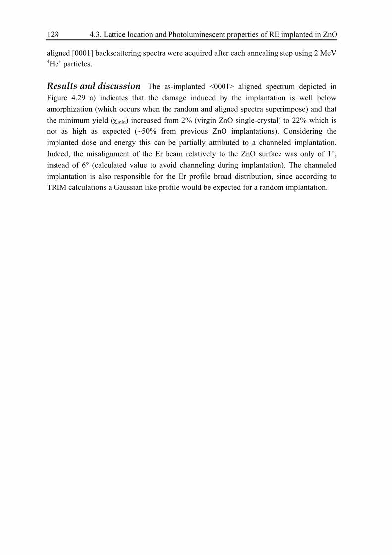
128 4.3. Lattice location and Photoluminescent properties of RE implanted in ZnO
aligned [0001] backscattering spectra were acquired after each annealing step using 2 MeV 4He+ particles. Results and discussion The as-implanted <0001> aligned spectrum depicted in Figure 4.29 a) indicates that the damage induced by the implantation is well below amorphization (which occurs when the random and aligned spectra superimpose) and that the minimum yield (χmin) increased from 2% (virgin ZnO single-crystal) to 22% which is not as high as expected (~50% from previous ZnO implantations). Considering the implanted dose and energy this can be partially attributed to a channeled implantation. Indeed, the misalignment of the Er beam relatively to the ZnO surface was only of 1°, instead of 6° (calculated value to avoid channeling during implantation). The channeled implantation is also responsible for the Er profile broad distribution, since according to TRIM calculations a Gaussian like profile would be expected for a random implantation.

4.3.1 Er implanted in ZnO 129
Figure 4.29 – Random and <0001>-aligned RBS spectra of a ZnO single-crystal implanted with 5x10¹⁵ Er+/cm2 (sample ZNOER1) for a) the as-implanted state and after a 800°C 30 min air annealing. Figure b) represents the spectra following the 1050°C annealing, from which the lattice recovery and Er surface segregation are evident. In both graphs the Er profile was 5x magnified.
While annealing at 600°C had little effect on the implantation damage, the 800°C air annealing induced already a considerable degree of lattice recovery (Figure 4.29 a)), as well as a slight Er surface segregation, which could explain the EC results obtained for temperatures above 800°C. Complete lattice recovery occurs following the 1050°C annealing (Figure 4.29 b)) yielding a χmin of only 4%. This effect is accompanied by a considerable Er diffusion towards the surface resulting in a surface peak and in the loss of approximately 50% of the implanted Er, possibly due to the formation of a volatile compound or to the Er in-diffusion to a depth beyond the RBS analyzing limits.
Figures 4.30 a) and b) show detailed angular scans performed along the [0001] direction. For these measurements the Zn window was set from 5 to 80 nm, incorporating
300 450 600 750 9000
1
2
3
4
5
6 Random <0001> axis as implanted <0001> ann. 800oC
a)
Er(x5)
Zn
Cou
nts(
/103 )
300 450 600 750 9000
1
2
3
4
5
6 Random <0001> axis ann. 1050oC <0001> axis virgin
b)
Channel
Er(x5)
Zn
Cou
nts(
/103 )

130 4.3. Lattice location and Photoluminescent properties of RE implanted in ZnO
thus the entire Er implanted depth region. In the as-implanted state (Figure 4.30 a)) the Er and Zn curves almost overlap, indicating that Er experienced exactly the same disorder caused by the implantation as the Zn sub-lattice. The 1050°C annealing resulted in a wider Zn angular scan, confirming the complete lattice recovery achieved at this temperature (Figure 4.30 b)).
Figure 4.30– a) Angular scan along the [0001] direction measured directly following implantation of 5x10¹⁵ Er+/cm2 (sample ZNOER1). Both Er and Zn atoms experience the same lattice disorder caused by the implantation and around 90% of Er is at substitutional sites along the c-axis. b) After the 1050°C annealing this fraction decreased to 25%, but the wider Zn curve and decrease of the minimum yield indicate a lattice recovery.
Moreover, the angular scans reveal that immediately after implantation 90% of the Er
atoms are located at sites within the c-axis. This value was estimated with equation (1- χEr) / (1- χZn). The Er regular fraction remaining at the implanted region decreased to 65% following the 800°C annealing and to 25 % after 1050°C (Figure 4.31).
-3 -2 -1 0 1 2 30,0
0,2
0,4
0,6
0,8
1,0
1,2
1,4a)
Nor
mal
ized
yie
ld
-3 -2 -1 0 1 2 30,0
0,2
0,4
0,6
0,8
1,0
1,2
1,4b)
Er Zn
Nor
mal
ized
Yie
ld
Angle(deg)
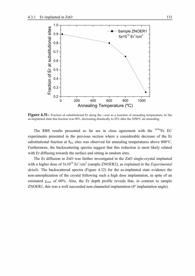
4.3.1 Er implanted in ZnO 131
0 200 400 600 800 10000.2
0.3
0.4
0.5
0.6
0.7
0.8
0.9
1.0
Frac
tion
of E
r at s
ubst
itutio
nal s
ites
Annealing Temperature (ºC)
Sample ZNOER1 5x10¹⁵ Er+/cm2
Figure 4.31– Fraction of substitutional Er along the c-axis as a function of annealing temperature. In the as-implanted state this fraction was 90%, decreasing drastically to 25% after the 1050°C air annealing.
The RBS results presented so far are in close agreement with the 167mEr EC experiments presented in the previous section where a considerable decrease of the Er substitutional fraction at SZn sites was observed for annealing temperatures above 800°C. Furthermore, the backscattering spectra suggest that this reduction is most likely related with Er diffusing towards the surface and sitting in random sites.
The Er diffusion in ZnO was further investigated in the ZnO single-crystal implanted with a higher dose of 5x10¹⁶ Er+/cm2 (sample ZNOER2), as explained in the Experimental details. The backscattered spectra (Figure 4.32) for the as-implanted state evidence the non-amorphization of the crystal following such a high dose implantation, in spite of an estimated χmin of 60%. Also, the Er depth profile reveals that, in contrast to sample ZNOER1, this was a well succeeded non-channeled implantation (6º implantation angle).

132 4.3. Lattice location and Photoluminescent properties of RE implanted in ZnO
300 450 600 7500
300
600
900
1200
1500
1800Sample ZNOER2 - 5x10¹⁶ Er+/cm2
O
Er
Zn
Cou
nts
Channel
Random As-implanted <0001> As-implanted <0001> 950ºC/air/30' Random 1050ºC/air/30' <0001> 1050ºC/air/30'
Figure 4.32 – Random and <0001>-aligned RBS spectra for crystal ZNOER2 implanted with 5x10¹⁶ Er+/cm2, for the as-implanted state and after 30 min air annealings at 950°C and 1050°C.
In contrast to the lower Er dose implanted crystal (ZNOER1), annealing in air at 950°C and 1050°C didn’t induce a considerable damage recovery nor a significant alteration of the Er depth profile. These results suggest that lattice recrystallization is closely related with Er segregation. For a lower implantation dose the lattice recrystallization drives out the implanted Er atoms, which was already reported by other authors [1] and can be attributed to the low solubility limit of rare-earths (RE) in ZnO. For the higher implantation dose the Er atoms are retained in the implanted region, which could be the reason for the inhibition of the recrystalization process. The Er atoms are randomly distributed and the formation of a new compound in the implanted region, that would prevent the lattice recovery from occurring, could not be ruled out. Previous PL and EC studies performed on Er doped Si revealed that this RE tends to form numerous Er-O complexes (clusters) [23]. Moreover, RBS studies on GaN co-implanted with O [24] revealed that for high Er implantation doses the RE was retained in the implanted region even after a 1000ºC annealing step and the lattice recovery was very slow. Inversely, a considerable Er surface segregation and better implantation damage annealing was observed on GaN samples without co-implanted O. Given these facts and since in ZnO the element O is naturally present at large concentrations, the formation of such Er-O complexes is likely to occur retaining thus the Er atoms in the implanted region. As a consequence, the lattice recovery from the implantation damage is hindered.
Conclusions The studies just described reinforce the fact that ZnO is highly resistant to implantation damage. Indeed, even for the high dose implanted crystal no amorphization

4.3.1 Er implanted in ZnO 133
was attained. Complete lattice recovery is achieved with the 1050ºC air annealing step, though it starts significantly at 800ºC. Along with the damage annealing, a progressive decrease of the substitutional Er fraction at Zn site is observed accompanied of Er segregation to the surface, indicating that all these processes are closely related. Indeed, in the single-crystal with high Er dose a low degree of damage annealing was registered as well as a small percentage of Er atoms surface segregation. It is suggested that the formation of Er-related compounds, such as Er-O clusters, inhibits the ZnO lattice from recovering and thus, diminishes the Er surface segregation. One is thus tempted to assume a correlation between the implantation dose and the diffusion process of implanted Er atoms, for the same annealing temperature. More precisely, once Er gets mobile and starts to diffuse it segregates to the surface in low implanted samples while for the high-dose implanted ones it forms Er-related clusters in the implanted region. All these findings suggest that a relatively high Er diffusion must have occurred in the ZnO crystal analyzed by EC after the 900°C annealing, explaining the considerable decrease of the Er fraction at SZn sites (section 4.3.1.1). 4.3.1.3 Er optical activation
The study of Er implanted in ZnO wouldn’t be complete without the evaluation of its
optical emission, given the promising application for optoelectronic devices. The Er lattice site location and the implantation damage can significantly influence the RE optical activation. Given the information gathered in the previous sections regarding these two issues, we are now in position to evaluate the Er optical emission as a function of annealing temperature.
Experimental details The single-crystals analyzed by RBS (ZNOER1 and ZNOER2) were furthermore studied with Photoluminescence (PL), to investigate the optical activation of the Er atoms after the annealing procedures. A third crystal (ZNOER3 – see table 3.3) implanted with only 5x10¹⁴ at/cm2 of stable Er was also studied, for the as-implanted state and following two 30 min air annealings at 600°C+1050°C (see table 3.5). This crystal was moreover investigated by RBS, but with such a low implantation dose no conclusions could be inferred from the experimental data in terms of Er segregation and lattice recovery. Notice that the pos-annealing PL measurements were done only after all the annealing steps. Results and discussion The PL emission spectra obtained at 77 K with below band-gap excitation for the low dose implantation samples (5x10¹⁴ at/cm2 and 5x10¹⁵ at/cm2) are represented in Figure 4.33. The fingerprint 1.54 μm emission band related with the 4I13/2 → 4I15/2 transition of Er3+ atoms was observed in both crystals only for the as-implanted state. The two air annealing treatments (600ºC+1050ºC) performed in these crystals eliminated the Er characteristic emission, indicating that the optically active Er-

134 4.3. Lattice location and Photoluminescent properties of RE implanted in ZnO
related centers were no longer present in ZnO. This might be related with the Er out-diffusion observed by RBS and the subsequent non-location of Er at SZn site (observed with EC). We reinforce that the PL measurements were undertaken only at the end of the annealing procedure (all annealing steps had been already performed).
Figure 4.33 – PL emission spectra obtained at 77 K with below band-gap excitation for as-implanted ZnO single-crystals with (a) 5x10¹⁵ Er+/cm2 (sample ZNOER1) and (b) 5x10¹⁴ Er+/cm2 (sample ZNOER3). The 1.54 μm emission band characteristic of Er+ atoms is clearly visible in the as-implanted state. The inset represents the PL obtained with above band-gap excitation for a virgin ZnO crystal, for the sample implanted with 5x10¹⁴ Er+/cm2 in the (1) as-implanted state and (2) after the two 30 min air annealing steps at 600°C + 1050°C and (3) for the crystal implanted with 5x10¹⁵ Er+/cm2 following two 30 min annealing steps at 600°C + 1050°C. [25]
The inset in Figure 4.33 represents the visible PL obtained with above band-gap excitation at room temperature. These measurements revealed that the spectra for the virgin and as-implanted crystals are dominated by two near band edge transitions (at 378 nm and 398 nm) and by a deep-level related green emission band peaked near 500 nm. With annealing procedures the near band edge emission disappears and a low energy shift of the green band to 520 nm is clearly observed. These results are in close agreement with similar studies performed with Cu atoms, where the different green PL mechanism in annealed and non-annealed crystals was explained by donor-to-acceptor (DAP) recombination processes [15] involving Cu+ (singly ionized acceptor) and Cu++ (neutral acceptor).
For the crystal implanted with higher dose (5x10¹⁶ Er+/cm2) the 1.54 μm Er band emission is also present in the as-implanted state. However, in contrast to the lower dose implanted samples, this band emission can still be observed after a 30 min air annealing at 800°C (Figure 4.34). This is most likely attributed to the non-diffusion of Er at this high

4.3.1 Er implanted in ZnO 135
implantation dose. Indeed, as observed from RBS, the Er depth profile did not suffer significant changes even after the high temperature annealing at 1050°C.
0.70 0.72 0.74 0.76 0.78 0.80 0.821E-4
1E-3
0.01
0.1
1
10
0.69 0.70 0.71 0.72
Ni3+
Cu2+
Er3+
PL in
tens
ity (a
.u)
Photon energy (eV)
Cu2+
0.706
0.709 0.711
0.74 0.75 0.76
Ni3+
0.7429
0.7549 0.7556
0.7564
0.76 0.78 0.80 0.82 0.84 0.86
Er3+0.8000.805
Figure 4.34 – PL infrared emission spectra obtained at 7 K using a 514.5 nm excitation for the ZnO single-crystal implanted with 5x10¹⁶ Er+/cm2 (sample ZNOER2) and annealed in air for 30 min at 800°C. Similar spectra were obtained for the as-implanted state. [26]
It is curious to notice that the Er3+ recombination is not the most intense emission in the studied spectral region. In fact, while for the lower dose samples no other recombination centres were detected, the infrared emission for the high dose sample indicates the presence of multiple deep level emissions (Figure 4.34). These could be attributed to an unintentionally grown contaminated crystal and/or to defects resulting from the implantation and annealing processes (such as Er-O clusters). From the literature it is well known that transition metal ions could act as efficient deep traps for free carriers due to their ability to occupy different charge states. In this sense, and according to previous reported data, the 0.711 eV recombination is tentatively assigned to the 2E → 2T2 intra-d shell transition of the Cu2+ (3d9) ion [27] and the 0.75 eV optical centre to the 4T2 → 4A2 transition of the Ni3+ (3d7) [28].
In the visible spectral region a few more optical centres were detected as can be seen from Figure 4.35. Namely, a 4S3/2 → 4I15/2 Er-related emission was observed (Figure 4.35 (b)) and the presence of Ni2+ was moreover confirmed by its 3T1(P) absorption band (1.879, 1.884 eV and 1.896 eV) [29] [30] presented in Figure 4.35 (c). The Fe3+ luminescence was also detected in the same spectral region with below band gap excitation [31] [32] (Figure 4.35 (d)).

136 4.3. Lattice location and Photoluminescent properties of RE implanted in ZnO
Figure 4.35 – (a) PL visible emission spectra obtained at 7 K with He-Cd excitation for the ZnO single-crystal implanted with 5x10¹⁶ Er+/cm2 (sample ZNOER2) and annealed in air for 30 min at 800°C. The (b) Er-related transition 4S3/2 → 4I15/2 can be clearly observed as well as the (c) self-absorption of intraionic Ni2+. Moreover, the (d) intraionic Fe3+ emission was detected with below band-gap excitation. [33] Conclusions The PL results presented above suggest that the 1.54 μm emission band associated with the 4I13/2 → 4I15/2 transition of Er3+ atoms is closely related with the diffusion of the Er atoms following annealing treatments. Indeed, this emission band was observed only in samples and/or annealing temperatures for which no Er diffusion took place (information extracted from RBS experiments). This phenomenon could be explained by the fact that Er diffusion induces a decrease of the substitutional fraction at Zn site, leading thus to the disappearance of the fingerprint Er emission band.
In the single-crystal implanted with higher dose of Er atoms a 4S3/2 → 4I15/2 Er-related emission was observed in the visible region of the emission spectrum. Moreover, several recombination centers were detected in this sample, both in the infrared and visible spectral regions. From the literature it was possible to assign these centers to the presence of transition metals, namely, Cu2+ and Ni3+ (infrared emission) and Ni2+ and Fe3+ (visible emission). The contamination of the ZnO single-crystal with these metals could have occurred during the growth process.
4.3.2 Tm implanted in ZnO
In this section the results obtained for Tm implanted in ZnO are presented. Although these studies are similar to the ones of Er, presented in the previous section, a more

4.3.2 Tm implanted in ZnO 137
thorough evaluation of the Tm behavior in ZnO was performed as a function of annealing temperature, resulting in interesting and important findings. The section starts with the results of the Tm lattice site location experiments and continues with the RBS and optical activation studies.
4.3.2.1 Tm lattice site location
Experimental details The lattice site location of implanted Tm in ZnO was investigated by means of EC, making use of the radioactive decay 169Yb ⎯→⎯32d 169Tm*
⎯⎯ →⎯ μs 0.66 169Tm (Figure A.8 in Appendix A). The recoil energy in the 169Yb → 169Tm* nuclear decay is less than 1.1 eV for which it is most likely that the 169Tm* atoms inherited the 169Yb lattice site. The subsequent nuclear decay 169Tm* → 169Tm is accompanied by conversion electron emission which was used in the EC measurements here presented.
To carry out this investigation a ZnO [0001] single-crystal grown by SCVT, O face, was implanted at CERN/ISOLDE with 3x10¹³ at/cm2 of the precursor 169Yb at 60 keV. Further implantation parameters can be found in table 3.1, sample ZNOEO9 (see table 3.3). The angular distributions of the conversion electrons emitted by 169Tm*, with energies of 100, 109, 118, 121, 139, 188, 248 and 198 keV, were recorded in the as-implanted state and following 10 min in-situ vacuum annealings at 300°C and 600°C and a 10 min ex-situ annealing in flowing O2 at 800°C (see table 3.5) to evaluate a possible lattice recovery improvement. As usual, the emission channeling patterns were measured around the [0001], [1102], [1101] and [2113] directions in order to achieve unambiguous information about the emitter lattice site. The experimental data was analyzed according to the procedure described in section 2.3.5., by comparing the experimental emission patterns with theoretical ones for 169Tm* at substitutional Zn sites (SZn) and O sites (SO) with varying root mean square displacement.
Results and discussion The experimental patterns and corresponding two-fraction fits of the theoretical yields are depicted in Figure 4.36 following the 300°C annealing. For this temperature around 95% of the Tm atoms were substitutional at the SZn site with rms displacements of 0.12-0.16 Å.

138 4.3. Lattice location and Photoluminescent properties of RE implanted in ZnO
-2
-1
0
1
2
-2 -1 0 1 2(a)
(0110)
experiment-2 -1 0 1 2
1.72 - 1.89 1.55 - 1.72 1.38 - 1.55 1.21 - 1.38 1.04 - 1.21 0.87 - 1.04 0.70 - 0.87 0.53 - 0.70
simulation for SZn sites
(e) [0001]
-2
-1
0
1
2
(1011)
(b)
(1120)
2.40 - 2.65 2.15 - 2.40 1.91 - 2.15 1.66 - 1.91 1.41 - 1.66 1.17 - 1.41 0.92 - 1.17 0.67 - 0.92
(f) [1102]
-2
-1
0
1
2(c)
(2021)
(1120)
(d)
2.15 - 2.37 1.94 - 2.15 1.72 - 1.94 1.50 - 1.72 1.29 - 1.50 1.07 - 1.29 0.86 - 1.07 0.64 - 0.86
(g) [1101]
[deg]-3 -2 -1 0 1-2
-1
0
1
2
(0110)
(1120)
-3 -2 -1 0 1
(h) [2113] 2.15 - 2.37 1.94 - 2.15 1.72 - 1.94 1.50 - 1.72 1.29 - 1.50 1.07 - 1.29 0.86 - 1.07 0.64 - 0.86
Figure 4.36 – Experimental emission channeling patterns of the 169Tm* conversion electrons around the (a) [0001], (b) [1102], (c) [1101] and (d) [2113] directions following the 300°C vacuum annealing. The theoretical patterns (e) to (h) that best fitted the experimental data indicate that approximately 95% of the Tm atoms were located at SZn with rms displacements ranging from 0.12 Å to 0.16 Å.
For all annealing temperatures the best fits were attained considering simply two fractions, namely, substitutional at SZn site and a random fraction responsible for an isotropic emission yield. There was no evidence of other regular lattice sites. Figures 4.37 (a) and (b) represent the average fraction of Tm atoms at SZn and the rms displacements from this site perpendicular to each direction as a function of the annealing temperature, respectively. The results reveal that up to the 600°C annealing temperature 95% of the Tm atoms were substitutional at non-ideal SZn sites and that this fraction decreased to 75% following the 800°C O2 annealing.
The rms displacements perpendicular to the symmetry directions decreased progressively up to the 600°C annealing temperature reaching values as low as the Zn and O atoms thermal vibrations. This indicates a progressive lattice recovery and a better Tm

4.3.2 Tm implanted in ZnO 139
incorporation at SZn sites. Nevertheless, the rms displacement values were raised by the 800°C O2 annealing.
0,6
0,8
1,0
O2 annealedvacuum annealed
(a)fra
ctio
n of
169*
Tm o
n S Zn
0 200 400 600 800
0,050,100,150,200,25(b)
annealing temperature TA [°C]
rms d
ispl
acem
ents
u1 [Å
]
⊥ [0001] ⊥ [1102] ⊥ [2113] ⊥ [1101]
Figure 4.37 – (a) Average fraction of Tm atoms substitutional at SZn site and (b) corresponding rms displacement perpendicular to each of the four symmetry directions as a function of the annealing temperature. Notice that the last annealing step at 800°C was performed in flowing O2.
Some illations can be extracted from the presented results. The Tm fraction decrease at SZn and corresponding rms displacement increase following the 800°C annealing might be related with Tm out-diffusion, as observed for Er implanted ZnO for temperatures at or above 800°C. Moreover, the fact that no annealing is necessary to incorporate Tm at the SZn site (95% of Tm at SZn in the as-implanted state) could be a consequence of both the low implanted dose and the high resistance of ZnO against the formation of defects by irradiation. Still, a better incorporation at SZn is achieved after 600°C, which could be related with the annealing of some structural defects in the Tm neighborhood. These questions were addressed via RBS studies that will be presented in the next sub-section.
To finalize, it is important to refer that these results are quite similar to the ones obtained for the rare-earth 167mEr. Indeed, for this isotope 75-90% of the Er atoms were substitutional at SZn up to the 700°C annealing temperature. The rms displacement values were of the same order of magnitude of the ones measured for Tm and a progressive decrease was observed up to 700°C. In the same way, the 800°C vacuum annealing resulted in a decrease of the Er fraction at SZn (to 75%) and an rms displacement increase. This suggests that substituting the 800°C vacuum annealing by a flowing O2 annealing does not result in significant changes in terms of the lattice site location and lattice recovery.

140 4.3. Lattice location and Photoluminescent properties of RE implanted in ZnO
Conclusions In the as-implanted state 95% of the Tm atoms were located at substitutional Zn site with rms displacement. This lattice site proved to be stable up to a 600ºC vacuum annealing, with progressive better incorporation of the RE at SZn. Annealing at 800ºC resulted in reduction of the Tm substitutional fraction (75%) along with an increase of the rms displacements from ideal SZn. This behavior was also observed in the Er implanted studies and could be related with Tm diffusion which, like Er, might start at this annealing temperature. The RBS experiments can bring further insight into this hypothesis. 4.3.2.2 Tm diffusion and damage annealing
The EC results previously presented motivated the Tm study in ZnO with respect to the investigation of Tm diffusion in this semiconductor and the lattice recovery from the implantation damage. These key subjects were evaluated with RBS not only as a function of the annealing temperature but also of the annealing duration. Further scenarios were considered in this evaluation, namely, direct annealing Vs successive annealing of the same sample, high temperature implantation, channeled implantation and different implantation doses.
Annealing temperature The effects of annealing temperature were evaluated in a [0001] ZnO single-crystal implanted at RT with 150 keV 5x10¹⁵ at/cm2 Tm ions according to the parameters presented in Table 3.3 (Implantation 1). The single-crystal was then sub-divided in four smaller samples (ZNOTM1, ZNOTM2, ZNOTM3 and ZNOTM4) which were air annealed for 30 min at different temperatures ranging from 800°C to 1050°C (see table 3.5). The RBS analysis was performed with a 2 MeV 4He+ collimated beam for the as-implanted state and following each of the annealing steps. The corresponding random and <0001> aligned backscattering spectra are shown in Figure 4.38.

4.3.2 Tm implanted in ZnO 141
300 450 600 7500
100
200
300
400
500
600Implantation 1 - 5x10¹⁵ Tm3+/cm2
O
Zn
Tm (x5)
Channel
Random <0001> As-Implanted <0001> 800ºC/air <0001> 950ºC/air <0001> 1050ºC/air
Figure 4.38 – Random and <0001>-aligned RBS spectra for ZnO single-crystals from Implantation 1 implanted with 5x10¹⁵ Tm3+/cm2, for the as-implanted state and after a single 30 min air annealing at 800°C, 950°C and 1050°C. The Tm signal was multiplied by 5 for better visualization.
The damaged region resulting from Tm implantation can be clearly distinguished in the
as-implanted aligned spectrum yielding a χmin of 43%. Though this value is far from amorphization, it is considerably higher than the usual 2% found for a virgin ZnO single-crystal. A defect density of 7x1016 cm-2 displaced Zn atoms was determined from the spectrum using the procedure described in Chapter 2. Annealing in air at 800°C did not induce a considerable lattice recovery, since a χmin of 32% and a defect density of 5x1016 cm-2 was still determined. However, the 950°C annealing resulted in a considerable decrease of the implantation damage, yielding a χmin of only 9% and a defect density of 0.9x1016 cm-2. The complete lattice recovery occurs at 1050°C with a χmin = 3%.
It is also important to remark that the Tm depth profile changed with increasing annealing temperature. Indeed, Tm diffusion towards the surface starts already at 800°C, but it is more pronounced following the 1050°C, after which 27% of the Tm atoms have segregated. For this temperature, similar results were found for the Er implanted ZnO single-crystals previously presented. Moreover these results confirm the hypothesis raised by the EC results: the decrease of the Tm fraction at regular SZn sites and the rms displacement increase following the 800°C O2 annealing could be related with Tm out-diffusion occurring already at this temperature.
The detailed angular scans performed along the [0001] direction indicate that following implantation Tm experiences the same disorder as the Zn sub-lattice (Figure 4.39 (a)), since the Tm and Zn curves overlap. The minimum yields found for both elements were χTm = 40% and χZn = 36%, which leads to 94% of Tm ions substitutional at the Zn site

142 4.3. Lattice location and Photoluminescent properties of RE implanted in ZnO
(SZn) along the c-axis (the equation (1-χTm) / (1-χZn) was used). This fraction decreased considerably to 30% after the 800°C annealing, which is a much lower value than the one determined from EC for the same temperature (75%). The fact that a much lower Tm dose was used in the EC experiments may explain this difference. Angular scans performed along the [0001] and [-1101] directions for the higher temperature (1050ºC) annealed sample revealed that, in spite of the Tm segregation, the fraction of Tm ions substitutional at Zn sites remained constant at 30% (the same as after the 800ºC annealing), as can be seen from Figure 4.39 (b) along the [0001] direction. The remaining Tm fraction is considered to be located in random sites. Moreover, it was found that in the surface segregation region of the 1050ºC air annealed crystal, only 15% of Tm is located at SZn sites (Figure 4.39 (b)). These angular scans confirmed furthermore the lattice recovery from the implantation damage, evident from the wider Zn curve.
-3 -2 -1 0 1 2 30,0
0,2
0,4
0,6
0,8
1,0
1,2
1,4(a)
Nor
mal
ized
Yie
ld
TmZn
-3 -2 -1 0 1 2 30,0
0,2
0,4
0,6
0,8
1,0
1,2
1,4
Surf.peak (Tm)
(b)
Nor
mal
ized
Yie
ld
Angle(deg)
TmZn
Figure 4.39 – a) Angular scans along the [0001] direction measured (a) following implantation of 5x10¹⁵ Tm3+/cm2 (Implantation 1) and (b) after the 1050°C air annealing.

4.3.2 Tm implanted in ZnO 143
The lattice recovery results suggest that an annealing temperature lower than 1050°C would be sufficient to recover the lattice without a significant Tm segregation. For this reason, a second ZnO single-crystal was implanted with the same dose of Tm ions (Implantation 4 in table 3.3) to evaluate the annealing temperature range 750°C-1050°C in greater detail. The crystal was afterwards cut in smaller samples that were annealed in air for 30 min at different temperatures.
The backscattering spectra obtained for the as-implanted state revealed that this implantation induced a higher damage in the ZnO crystal (Figure 4.40). Indeed a χmin of 53% was found versus the 43% determined for the crystal from Implantation 1. This could be attributed to a higher fluence used during Implantation 4, since the virgin ZnO single-crystals were of equivalent quality.
300 450 600 7500
100
200
300
400
500
600
O
Implantation 4 - 5x10¹⁵ Tm 3+ /cm2
Zn
Tm (x5)
Cou
nts
Channel
Random <0001> As-Implanted <0001> 750ºC/air/30 min <0001> 850ºC/air/30 min <0001> 900ºC/air/30 min <0001> 950ºC/air/30 min
Figure 4.40 – Random and <0001>-aligned RBS spectra for ZnO single-crystals from Implantation 4 implanted with 5x10¹⁵ Tm3+/cm2, for the as-implanted state and after a single 30 min air annealing at 750°C, 850°C, 900°C and 950°C. The Tm signal was multiplied by 5 for better visualization.
In spite that the implantation conditions were not the same as for Implantation 1, there
are still some remarks that can be drawn in terms of lattice recovery. More precisely, the spectra in Figure 4.40 evidence that the lattice starts to recover already at 750°C (χmin of 29 % and defect density of 3.4x10¹⁶ at/cm2) and that no significant changes occur up to the 950°C annealing.
However, Tm segregation was observed only after the 900°C annealing, instead of 800°C detected in Implantation 1. This could be attributed to the higher implantation damage present in the Implantation 4 crystal which prevented Tm from segregating to the
144 4.3. Lattice location and Photoluminescent properties of RE implanted in ZnO
surface at lower temperatures. This segregation increased further with the 950°C annealing, reaching 21% Vs the 14% registered for the Implantation 1 sample annealed at the same temperature. This difference is curious if one notices that in fact for this annealing temperature the single-crystal from Implantation 1 suffered a higher lattice recovery than the one of Implantation 4 for the same temperature: χmin (Imp1) = 7% Vs χmin (Imp.4) = 22%. These results point towards a faulty temperature control of the 950ºC annealing step performed in Implantation 1 which was most probably done at a higher temperature (possibly around 1000ºC).
Annealing duration The influence of annealing duration for a same temperature was investigated in two samples from Implantation 1, namely, the samples annealed at 950°C and 1050°C. These samples were thus subjected to a second air annealing at the same temperature but for a period of 60 min (isothermal annealing) (see table 3.5).
The <0001>-aligned RBS spectra depicted in Figure 4.41 (a) and (b) reveal no modifications in terms of lattice recovery. Indeed, the calculations based on the spectra yielded for the 950°C annelings χmin (30’) = 7% Vs χmin (60’) = 6.8%. In the same way, for the 1050°C annealings the values obtained were χmin (30’) = 3% Vs χmin (60’) = 4%. These results confirm that temperature is the important factor in implantation damage annealing and not the annealing duration. Nevertheless the same statement is not true for the Tm segregation dynamics. Whereas the second 950°C annealing did not induce further Tm segregation to the surface, the 60 min 1050°C annealing step resulted in an increase of this fraction from 27% to 81%. This points out to the following: for Tm out-diffusion not only the annealing temperature is important, but also the duration of the annealing treatment. It is also interesting to point out that none of the second step annealings here presented resulted in crystal degradation.
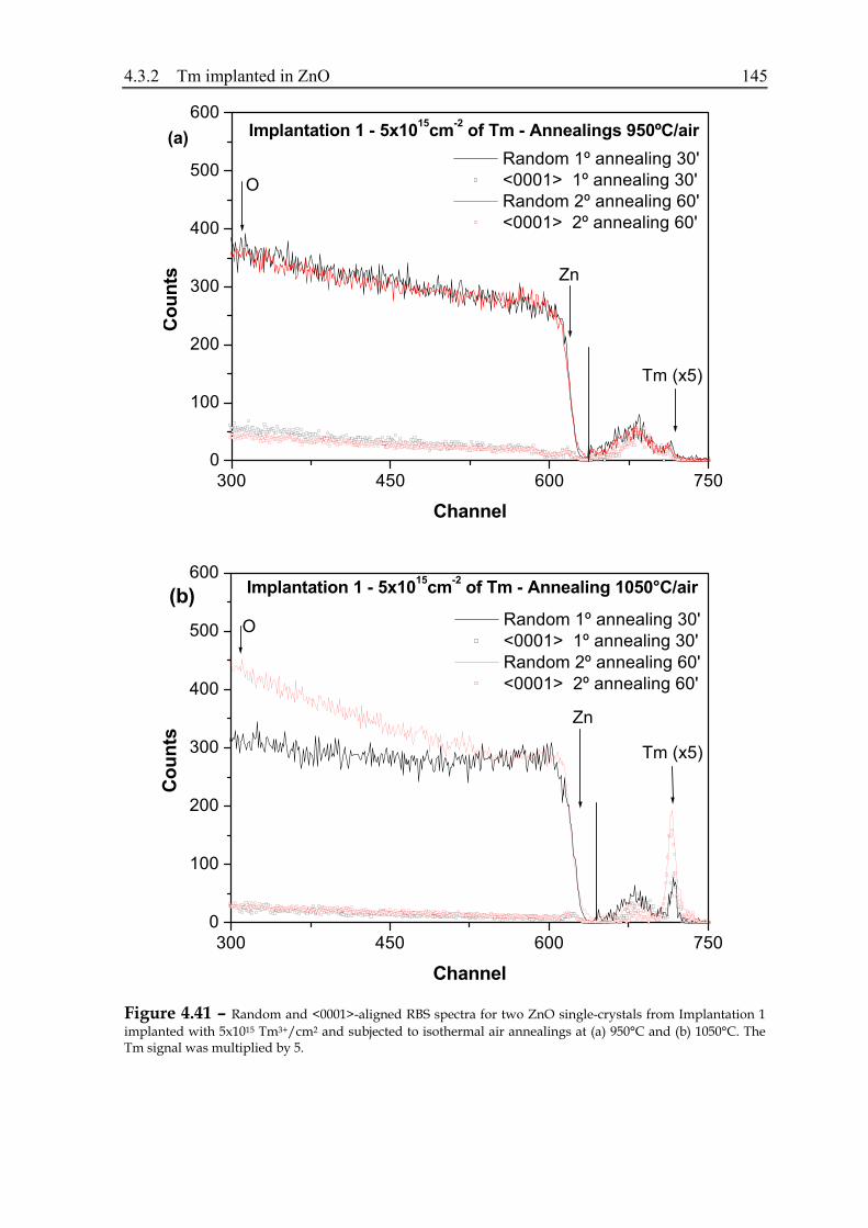
4.3.2 Tm implanted in ZnO 145
300 450 600 7500
100
200
300
400
500
600(a)
O
Implantation 1 - 5x1015cm-2 of Tm - Annealings 950ºC/air
Zn
Tm (x5)
Cou
nts
Channel
Random 1º annealing 30' <0001> 1º annealing 30' Random 2º annealing 60' <0001> 2º annealing 60'
300 450 600 7500
100
200
300
400
500
600(b)
O
Implantation 1 - 5x1015cm-2 of Tm - Annealing 1050°C/air
Zn
Tm (x5)
Cou
nts
Channel
Random 1º annealing 30' <0001> 1º annealing 30' Random 2º annealing 60' <0001> 2º annealing 60'
Figure 4.41 – Random and <0001>-aligned RBS spectra for two ZnO single-crystals from Implantation 1 implanted with 5x10¹⁵ Tm3+/cm2 and subjected to isothermal air annealings at (a) 950°C and (b) 1050°C. The Tm signal was multiplied by 5.
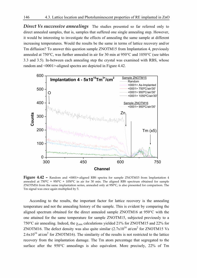
146 4.3. Lattice location and Photoluminescent properties of RE implanted in ZnO
Direct Vs successive annealings The studies presented so far referred only to direct annealed samples, that is, samples that suffered one single annealing step. However, it would be interesting to investigate the effects of annealing the same sample at different increasing temperatures. Would the results be the same in terms of lattice recovery and/or Tm diffusion? To answer this question sample ZNOTM15 from Implantation 4, previously annealed at 750°C, was further annealed in air for 30 min at 950°C and 1050°C (see tables 3.3 and 3.5). In-between each annealing step the crystal was examined with RBS, whose random and <0001>-aligned spectra are depicted in Figure 4.42.
300 450 600 7500
100
200
300
400
500
600
O
Implantation 4 - 5x10¹⁵Tm3+/cm2
Zn
Tm (x5)
Cou
nts
Channel
Sample ZNOTM15 Random <0001> As-Implanted <0001> 750ºC/air/30' <0001> 950ºC/air/30' <0001> 1050ºC/air/30'
Sample ZNOTM16
<0001> 950ºC/air/30'
Figure 4.42 – Random and <0001>-aligned RBS spectra for sample ZNOTM15 from Implantation 4 annealed at 750°C + 950°C + 1050°C in air for 30 min. The aligned RBS spectrum obtained for sample ZNOTM16 from the same implantation series, annealed only at 950°C, is also presented for comparison. The Tm signal was once again multiplied by 5.
According to the results, the important factor for lattice recovery is the annealing temperature and not the annealing history of the sample. This is evident by comparing the aligned spectrum obtained for the direct annealed sample ZNOTM16 at 950°C with the one attained for the same temperature for sample ZNOTM15, subjected previously to a 750°C air annealing. Indeed, the χmin calculations yielded 21% for ZNOTM15 and 22% for ZNOTM16. The defect density was also quite similar (2.7x10¹⁶ at/cm2 for ZNOTM15 Vs 2.6x10¹⁶ at/cm2 for ZNOTM16). The similarity of the results is not restricted to the lattice recovery from the implantation damage. The Tm atom percentage that segregated to the surface after the 950°C annealings is also equivalent. More precisely, 22% of Tm

4.3.2 Tm implanted in ZnO 147
segregated in sample ZNOTM15, annealed at 750°C+950°C, and 21% in sample ZNOTM16, annealed directly at 950°C.
Analogous conclusions can be delineated for the final 1050°C annealing temperature, reinforcing the above statements. Though there isn’t any sample from Implantation 4 annealed directly at 1050°C, the results for sample ZNOTM15 following the final 1050°C annealing step can still be compared to some extent to the Implantation 1 sample annealed directly at 1050°C. It is important to remember that the Tm implanted dose was the same in both implantation series. In fact, the χmin determined from the <0001>-aligned spectra yielded 3% for the Implantation 1 sample annealed only at 1050°C, and 6% for sample ZNOTM15, annealed at 750°C + 950°C + 1050°C. Moreover, 27% of the Tm atoms segregated to the surface in the Implantation 1 sample versus 35% found for sample ZNOTM15.
Given these results it seems reasonable to conclude that in terms of lattice recovery from the implantation damage and Tm surface segregation it is equivalent to anneal a ZnO single-crystal directly to a given temperature or to anneal it at progressively increasing annealing temperatures. The effects are therefore independent of the sample’s annealing temperature history. High temperature implantation The effects of high temperature implantation were evaluated on a ZnO single-crystal implanted at 450°C with a nominal dose of 5x10¹⁵ at/cm2 of Tm3+ ions at 150 keV (Implantation 2 in table 3.3). The as-implanted random spectrum from Figure 4.43 indicates firstly that the Tm implanted dose was not exactly 5x10¹⁵ at/cm2, as intended, but 8x10¹⁵ at/cm2. This was attributed to a miscarried implantation where the fluence was not accurately controlled. This means that care is needed when comparing these results with the ones presented previously for samples implanted with 5x10¹⁵ at/cm2.
Nevertheless, some remarkable findings can still be extracted from these experiments. For instance, if we take into account the fact that this crystal was implanted with a Tm dose superior to the one of Implantation 4 it is interesting to notice that the damage induced by both implantations is practically the same, since a χmin of 53% was determined for Implantation 4 in the as-implanted state and 51% for the Implantation 2 crystal. Given the higher implanted dose of Implantation 2, this suggests that the 450°C implantation temperature was beneficial for implantation damage reduction, as a higher χmin was expected for this implantation dose.

148 4.3. Lattice location and Photoluminescent properties of RE implanted in ZnO
300 450 600 7500
100
200
300
400
500
600
O
Zn
Tm (x5)
Implantation 2 - 8x10¹⁵ Tm3+/cm2 (Timpl = 450ºC)C
ount
s
Channel
Random <0001> As-Implanted
Figure 4.43 – Random and <0001>-aligned RBS spectra for a ZnO single-crystal implanted with 8x10¹⁵ at/cm2 of Tm3+ ions. The Tm signal was once again multiplied by 5.
This sample was further annealed at 800°C in air for 30 min, but only Photoluminescence studies were performed which will be presented at a later stage.
Channeled implantation When an implantation is carried out a Gaussian like depth profile of the implanted atoms is usually highly desirable, since it is easier to modulate for future data analysis. This is achieved by applying a misalignment of around 6° between the implantation atoms beam and the normal surface of the crystal. In this work, though, a different problematic was investigated. More precisely, the implantation damage resulting from a non-Gaussian implantation depth profile was evaluated following a channeled Tm implantation in ZnO. A ZnO single-crystal was thus implanted with 5x10¹⁵ at/cm2 at RT and 150 keV with a misalignment of less than 1° (Implantation 3 in table 3.2).
The results obtained for the as-implanted state revealed a drastic reduction of the implantation damage when compared with random implantations for the same dose (Figure 4.44). A χmin of only 20% and a defect density of 1.8x1016 cm-2 displaced Zn atoms were found. Moreover, as expected, the implanted atoms are distributed deeper into the sample and within a broader region.

4.3.2 Tm implanted in ZnO 149
300 450 600 7500
100
200
300
400
500
600
O
Zn
Tm (x5)
Implantation 3 - 5x10¹⁵ Tm3+/cm2 - As-Implanted
Cou
nts
Channel
Random (Random implantation) <0001> (Random implantation)
Random (Channeled Implantation) <0001> (Channeled implantation)
Figure 4.44 – RBS spectra for random and <0001>-aligned implantations of two ZnO single-crystals implanted with 5x10¹⁵ at/cm2 of Tm3+ ions. The Tm signal was multiplied by 5.
Dose effects (high implantation dose) The results presented so far referred to a Tm implantation dose of 5x10¹⁵ at/cm2. With the aim of searching for possible dose effects, the Tm diffusion and lattice recovery were furthermore investigated on a higher dose implanted ZnO single-crystal. The Tm dose implanted to carry out this study was 5x10¹⁶ at/cm2 at 150 keV (Implantation 5 in table 3.2). The crystal was subsequently divided in smaller samples and each of them subjected to a single 30 min air annealing step at 800°C, 900°C and 950°C.
The higher dose implantation induced a higher defect density than the lower dose implantations performed previously (Figure 4.45). Also, the surface defect peak is quite high, evidencing the considerably elevated implantation damage.

150 4.3. Lattice location and Photoluminescent properties of RE implanted in ZnO
300 450 600 7500
100
200
300
400
500
600
O
Zn
Tm
Implantation 5 - 5x10¹⁶ Tm3+/cm2
Cou
nts
Channel
Random <0001> As-Implanted <0001> 800ºC/air/30' <0001> 900ºC/air/30' <0001> 950ºC/air/30'
Figure 4.45 – RBS spectra for a ZnO single-crystal implanted with 5x10¹⁶ at/cm2 of Tm3+ ions and annealed in air for 30 min at 800°C, 900°C and 950°C.
In the as-implanted state a χmin of 60% and 1.1x10¹⁷ at/cm2 of displaced Zn atoms were found (Vs 43% and 7.1x10¹⁵ at/cm2, respectively, for the 5x10¹⁵ Tm3+/cm2 implanted samples). The 800°C and 900°C air annealings did not produce a considerable lattice recovery, except for the surface defect peak. This behavior was also observed in the 5x10¹⁵ Tm3+/cm2 implanted crystals. The 950°C annealing resulted in a higher damage decrease yielding a χmin of 38% and 4.3x10¹⁶ at/cm2 of displaced Zn atoms. Still, this recovery was not as pronounced as the registered at the same temperature for the Implantation 1 sample (χmin = 9%). Actually, the results are closer to Implantation 4 for this temperature (χmin = 22%), being the difference attributed to the lower implanted dose. As referred earlier, this points out once again for a possible problem in controlling the 950°C annealing temperature performed on the Implantation 1 crystal. It is possible that in fact this crystal was annealed at a higher temperature, since all crystals used in the experiments here reported were of equivalent quality.
An interesting aspect of this experiment is the non-segregation of Tm at least up to the 950°C annealing temperature. This same behavior was registered for Er implanted ZnO single-crystals, for the same dose (section 4.3.1.2). As exposed earlier for the case of Er, this was attributed to the possible formation of Er-O clusters [23] [24] that inhibit the RE segregation and, therefore, the lattice recovery from the implantation damage. Since Tm

4.3.2 Tm implanted in ZnO 151
and Er are chemically similar the formation of Tm-O clusters is suggested in these higher dose implanted crystals.
A comparison of the results for the two different implanted doses is possibly easier by analyzing the graphs in Figure 4.46 (a) and (b). As is clearly seen, the χmin obtained for the samples implanted with 5x10¹⁶ Tm3+/cm2 is always higher than the corresponding values determined for the lower dose implanted samples. This was already expected, since the defects density produced by the implantation was considerably higher in the as-implanted state. Nevertheless, the χmin variation with the increasing annealing temperature is quite similar for both implantation doses. Once again, it is important to reinforce that the 950°C air annealing carried out in Implantation 1 might have occurred at a higher temperature, since it does not follow the same trend registered for the other Implantations. These same comments are valid for the defect density representation.

152 4.3. Lattice location and Photoluminescent properties of RE implanted in ZnO
0 700 800 900 1000 11000.0
0.2
0.4
0.6
0.8(a)
30' annealings5x1016 at/cm2
5x10¹⁵ at/cm2
Impl.4 - 30' annealings Impl.4 - Sample ZNOTM15
(750ºC+950°C+1050°C)
χ min
Annealing Temperature (ºC)
Impl.1 - 30' annealings Impl.1 - 60' annealings
0 700 800 900 10000,0
2,0
4,0
6,0
8,0
10,0
12,0(b)
30' annealings5x1016 at/cm2
5x10¹⁵ at/cm2 Impl.1 - 60' annealings Impl.4 - 30' annealings Impl.4 - Sample ZNOTM15
(750ºC+950°C+1050°C)
Dde
fect
s (x1
016 a
t/cm
2 )
Annealing Temperature (ºC)
Impl.1 - 30' annealings
Figure 4.46 – (a) Minimum yield χmin and (b) defect density Ddefects as a function of the annealing temperature for the RT random Tm implantations performed on ZnO single-crystals with doses of 5x10¹⁵ at/cm2 and 5x10¹⁶ at/cm2.
Conclusions The RBS studies discussed above confirm the high resistance of the ZnO crystal to implantation damage. Indeed, no amorphization of the crystal was detected, even

4.3.2 Tm implanted in ZnO 153
following high dose implantations. Air annealing induces a progressive lattice recovery with increasing temperature. Complete damage annealing was achieved after the 1050ºC annealing step only in samples with low implantation Tm doses. For higher implantation doses no significant lattice recovery was observed up to this temperature.
The lattice recovery is accompanied by Tm segregation towards the surface, starting already at 800ºC annealing temperature. This explains the EC results presented earlier in this section, where the Tm diffusion at 800ºC was proposed. No Tm segregation was observed in the samples implanted with higher dose of Tm, indicating that lattice recovery and RE segregation are closely related. More precisely, it is proposed that the formation of Tm-O clusters in this high Tm dose implanted crystal retains the Tm atoms at the implanted region and, therefore, reduces the lattice recovery.
Isothermal annealings revealed that the important factor for lattice recovery is the annealing temperature rather than the annealing duration. The same is not true in terms of Tm segregation: the longer the annealing, the higher the percentage of Tm atoms that segregate to the surface. Also, these two processes (lattice recovery and Tm segregation) are independent of the sample’s annealing history. Moreover, the damage induced by implantation can be considerably reduced via a channeled implantation and/or implanting at a temperature above RT (450ºC, for instance).
4.3.2.3 Tm optical activation
The photoluminescent properties of Tm implanted ZnO single-crystals were investigated by means of PL in some of the samples referred in the previous section, from both implantation doses (5x10¹⁵ at/cm2 and 5x10¹⁶ at/cm2). Within the ZnO band-gap, the Tm3+ ion has a ground state manifold 3H6 and excited manifold states 3F4, 3H5, 3H4, 3F3, 3F2 and 1G4. For GaN, a semiconductor with structure and band-gap similar to ZnO, the intraionic Tm3+-related emission has been attributed to the 1G4→3H6, 1G4→3F4 and 3H4→3H6 transitions, in the blue, red and near infrared, respectively [34-37].
Low implantation dose (5x10¹⁵ at/cm2) Tm optical activation was firstly investigated in the Implantation 1 samples (see table 3.2), for the as-implanted state and following 30 min air annealings at 800°C, 950°C and 1050°C. The 13 K PL spectra obtained under He-Cd excitation revealed that no luminescence was present in the as-implanted sample, suggesting that for this fluence and implantation temperature thermal annealings are needed to reduce the lattice damage and promote the rare-earth ion’s optical activation. Indeed, following the 800°C annealing, the partial damage recovery is evident by the presence of the typical near band edge (NBE) emission in ZnO (Figure 4.47). Moreover, this spectral region presents notorious differences in comparison to the virgin sample PL.

154 4.3. Lattice location and Photoluminescent properties of RE implanted in ZnO
Figure 4.47 – 13K PL spectra obtained with He-Cd excitation for (a) a virgin ZnO single-crystal and (b) samples implanted at RT with 5x10¹⁵ Tm3+/cm2 and annealed for 30 min in air at 800°C (ZNOTM1), 950°C (ZNOTM2) and 1050°C (ZNOTM3). The red rectangle demarks the Tm3+ intraionic-related emission 3H4→3H6 observed for the 800°C annealed sample. It can be better seen in Figure 4.47. The green rectangle denotes the laser line. [33]
Despite the partial damage recovery, a green band at ~2.45 eV and a red band ~1.8 eV are clearly present for some of the air annealed samples. The green band can be observed already in the virgin sample and is nearly suppressed by the lower dose Tm implantation and air annealing at 800°C. Though it was recently suggested that this green band is VO related [38] [39], other authors suggest that it might be Zni related. The above referred intensity decrease of the 2.45 eV green band could thus be related with a predominant clustering of VO and/or Zni resulting from the implantation. A structured green band at 2.43 eV, possibly related with Cu impurities [40] [41] or to VZn [42], is observed for the higher annealing temperatures at 950°C and 1050°C. This suggests that the transition metal ions intrinsically present in the virgin single-crystal assume an important role following these annealing procedures.
Simultaneously, a broad red band ~1.8 eV is identified already after the 800°C annealing. Broad bands in the red spectral region were reported previously and correlated with Zn deficiency [39]. More recently it was associated with the migration of host atom interstitials [43]. Since following implantation and low temperature annealing a high defect density of displaced Zn atoms is observed (from RBS measurements), it is likely to assume that the 1.8 eV red band originates on Zn-related defects induced by implantation. This band is enhanced with the 950°C air annealing whereas the Tm3+- related emission vanishes, which could be attributed to an increase of non-radiative paths or a decrease on the efficiency of the excitation processes. Moreover, since the VO and/or Zni related green band emission is not observed after this annealing temperature, it is reasonable to point out
ZNOTM1
ZNOTM2
ZNOTM3
Energy (eV) Energy (eV)
Virgin Sample Tm implanted Samples

4.3.2 Tm implanted in ZnO 155
to their participation in the formation of a defect complex responsible for the 1.8 eV red band.
Tm optical activation is promoted by the 800°C air annealing. The intraionic Tm-related emission is dominated by the 3H4 → 3H6 near infrared transition at 1.56 eV (Figure 4.48 – sample ZNOTM1). The blue intraionic emission 1G4→3H6, typically observed in Tm doped GaN, was not detected in this ZnO sample. The well-resolved multi-lines are due to the weak crystal field splitting of the spin-orbit multiplets. Assuming that, at 13 K, only the excited multiplet lowest level is populated, 9 ground state transitions are expected if the ion is under a hexagonal crystalline field, 10 for a tetragonal field and 13 for a lower symmetry [44]. Although the fine structure of the PL spectra in Figure 4.48 gives evidence of Tm incorporation in regular crystalline surroundings, the number of observed fluorescence lines cannot account for a single Tm-related optical centre, suggesting the presence of multi Tm-related optical centers. A similar behavior was found for RE doped GaN [34-37, 45, 46].
Figure 4.48 – 13K Tm-related PL spectra observed for samples implanted at (a) RT (ZNOTM1) and (b) 450°C (ZNOTM11), with 5x10¹⁵ Tm3+/cm2. Both samples were air annealed at 800°C.
In spite of the high intensity observed after the 800°C air annealing, the Tm optical activation quenches with increasing annealing temperature (Figure 4.47 (b)). This could be attributed to the prominent Tm out-diffusion observed from RBS analysis for annealing temperatures above 950°C. However, RBS results have also shown that, independently of the Tm segregation percentage, a constant fraction of approximately 30% of Tm ions remain incorporated in SZn sites for all samples in Figure 4.47 (air annealed at 800°C, 950°C and 1050°C). Two main aspects must then be thought through to find the cause for the Tm intraionic-emission. Firstly, if the emission truly arises from Tm3+ ions at SZn sites then changes in the ions surroundings must occur with increasing annealing temperature,
ZNOTM11
ZNOTM1

156 4.3. Lattice location and Photoluminescent properties of RE implanted in ZnO
such as, loss of charge compensation mechanisms that would result in the observed emission quenching. Secondly, since only 30% of Tm ions are located at SZn sites one cannot exclude that the intraionic-emission results from Tm ions incorporated at random sites within high defect density regions, which change with the increasing annealing temperature. Taking into account that the well-defined Tm-related lines are typically from ions placed at regular lattice sites, the first hypothesis seems more plausible. That is, it is suggested that the emission is due to Tm ions placed at SZn sites in close vicinity to a defect/impurity region that would be responsible for both the ion accommodation and charge compensation mechanisms. Then, if with increasing annealing temperature this defect/impurity region changes, the lattice will lose its ability for ion accommodation, promoting the surface segregation and affecting the charge compensation mechanisms. Nevertheless, it is clear that defect/impurity regions and a partial damage recovery play an important role on Tm optical activation.
The Tm optical activation was furthermore investigated in the sample implanted at 450°C with 5x10¹⁵ Tm3+/cm2 and annealed at 800°C (Figure 4.48 – Sample ZNOTM11). The Tm3+-related emission is also present in this crystal with high intensity and again the 2.45 eV VO/Zni – related green band is absent (see Figure 4.51 ahead). Instead, a broad emission at 2.3 eV is clearly identified. This was recently found in Zn-annealed ZnO samples and it is assumed to be related with the presence of deep donors that are commonly observed in electrical measurements [41]. Other authors suggest that this band corresponds to a spin-dependent electron capture process involving the shallow donor and a positively charged VO [43].
This sample was also evaluated with low temperature time-resolved PL together with a virgin ZnO single-crystal (Figure 4.49). The intention was to observe a distant donor-acceptor pair (DAP) recombination at 3.22 eV, which is one of the main transitions observed at low temperature. The spectra in Figure 4.49 were obtained with above band-gap excitation performed after a time delay A within a time window B of the pulse lamp.

4.3.2 Tm implanted in ZnO 157
Figure 4.49 – Steady state (SS) PL and time resolved spectra obtained with above band-gap excitation for a virgin ZnO single crystal and sample ZNOTM11 (implanted at 450°C with 5x10¹⁵ Tm3+/cm2 and annealed at 800°C/air/30 min).
While for the virgin sample the peak position of the distant pair recombination is
difficult to observe due to the DAP overlap with a slow emission band at 3 eV [47], for the sample implanted at 450°C, where this slow emission is absent, the distant pair recombination can be clearly identified at 3.12 eV. With this data it is possible to locate the acceptor level responsible for this emission 250 meV above the valence band, assuming that the donor-acceptor level is 67 meV below the conduction band [47]. This donor level was accepted because the shallowest H-related donor level is presumably absent after annealing procedures [48].
One of the main aspects arising from the PL studies exposed so far is that Tm optical activation occurs in RT and 450°C low fluence implanted samples after annealing at 800°C. Moreover, different optical Tm-related centers occur in both samples. This feature is further evident from the temperature dependence of the different PL lines that correspond to the different optical centers. Inspection of the results presented in Figure 4.50 reveals that intraionic Tm-related luminescence was detected up to almost room temperature. More precisely, two highest intensity lines at 1.556 and 1.541 eV are visible in the sample implanted at RT (ZNOTM1). Minor intensity lines can also be resolved for 1.562 eV, 1.561 eV, 1.560 eV, 1.559 eV, 1.558 eV, 1.557 eV, 1.554 eV, 1.552 eV, 1.551 eV, 1.547 eV, 1.545 eV, 1.535 eV, 1.532 eV and 1.529 eV. Other unresolved lines could also be observed. For the 450°C implanted sample (ZNOTM11) some of the observed lines present a larger full width half maximum than the ones detected for ZNOTM1. Nevertheless, the highest intensity lines occur similarly at 1.559 and 1.544 eV. Minor lines were observed at energies of 1.577 eV, 1.574 eV, 1.567 eV, 1.562 eV, 1.561 eV, 1.560 eV, 1.558 eV and 1.547 eV. At least six of the observed lines are coincident in both samples, suggesting that the same optical centre is present in both cases. Furthermore, the spectral
ZNOTM11 SS

158 4.3. Lattice location and Photoluminescent properties of RE implanted in ZnO
analysis and evolution of the peak lines with temperature indicate that at least two optical-related centers must be present.
Figure 4.50 – Temperature dependence of PL spectra for samples ZNOTM1 (full line) and ZNOTM11 (dashed line) implanted at RT and 450°C, respectively, with 5x10¹⁵ Tm3+/cm2 and annealed at 800°C/air/30 min. [49].
High implantation dose (5x10¹⁶ at/cm2) In contrast to the low dose Tm implanted samples, the acquired PL spectra revealed that the 1.8 eV red band was not present in any of the higher dose implanted and annealed crystals. However, the 2.45 eV VO/Zni-related green band was detected in the 800°C annealed sample (ZNOTM6), reinforcing the possible participation of these intrinsic defects in the complex defect formation responsible for the 1.8 eV red band (Figure 4.51). The green structured Cu-related emission (2.43 eV) was not detected as well.

4.3.2 Tm implanted in ZnO 159
Figure 4.51 – 14K steady state PL spectra for ZnO samples implanted at RT with 5x10¹⁶ Tm3+/cm2 and annealed in air for 30 min at 800°C (ZNOTM6), 900°C (ZNOTM7) and 950°C (ZNOTM8). Sample ZNOTM11 was implanted at 450°C with 5x10¹⁵ Tm3+/cm2 and annealed at 800°C. [33]
With increasing annealing temperature (900°C and 950°C) a broad violet band is
observed at 3.15 eV, which has been tentatively attributed to be VZn – related and/or to a doubly positively charged Vo++ [48]. Since in the 800°C annealed sample, for which the 2.45 eV VO – related green band is present, the 3.15 eV violet band is absent, the explanation for the later is mostly related with VZn rather than with VO
++. Moreover, the absence of the violet band for this annealing temperature clearly indicates that the zero-phonon line of the 2.45 eV band occurs nearby the conduction band, in contrast to the one corresponding to the structured Cu-related green band. This was also observed by other authors [50].
Contrary to the low Tm dose implanted samples, Tm optical activation is achieved already in the as-implanted state (Figure 4.52) for samples implanted with 5x10¹⁶ Tm3+/cm2. However, the emission is several orders of magnitude lower, which could be attributed to the presence of non-radiative paths introduced by the implantation damage. Upon annealing at 800°C, 900°C and 950°C new optical Tm-related centres appear, the luminescence intensity being maximal after 800°C and decreasing progressively for the higher annealing temperatures. This behaviour was also observed for the low fluence Tm implanted crystals which were also the ones to register the highest Tm luminescence intensity.
ZNOTM11
ZNOTM6
ZNOTM7
ZNOTM8
Virgin sample

160 4.3. Lattice location and Photoluminescent properties of RE implanted in ZnO
Figure 4.52 – 13K Tm-related PL spectra with above band-gap excitation for ZnO single-crystals implanted at RT with 5x10¹⁶ Tm3+/cm2 for the as-implanted state (ZNOTM9) following 30 min air annealings at 800°C (ZNOTM6), 900°C (ZNOTM7) and 950°C (ZNOTM8).
In the low fluence implanted samples, the Tm-related emission after 800°C annealing and the subsequent intensity decrease were attributed either to Tm atoms placed at random positions or to Tm ions at regular SZn sites with different environments promoted by the annealing. A similar scenario can be drawn for the crystals implanted with 5x10¹⁶ Tm3+/cm2, since following the annealing steps several of the Tm-related lines observed in the as-implanted state are no longer present. With the used excitation conditions and in this particular spectral region the Tm intraionic luminescence is expected to be dominated by the 3H4→3H6 transition. The observation of different spectral features after the annealing treatments suggests that either the Tm ion environment has changed or that the emission arises from new Tm complexes.
Conclusions In the ZnO single-crystals implanted with 5x10¹⁵ Tm3+/cm2 the Tm optical activation occurs after the 800ºC air annealing and decreases progressively with the subsequent annealing procedures. In contrast, for the higher dose implanted samples, Tm optical emission is observed already in the as-implanted state, but is enhanced also by the 800ºC annealing. For both implantation doses, Tm-related emission is dominated by the 3H4→3H6 transition. This was attributed to Tm atoms substitutional at Zn site with defect configurations in the near neighborhood that change with the annealing procedure, resulting in the different Tm-related optical centers observed in the PL measurements. From the behavior of the green (2.45 eV) and red (1.8 eV) bands as a function of annealing temperature it is proposed that the VO and/or Zni intrinsic defects (responsible for the green band) play an important role in the defect complexes responsible for the red band.
Inte
nsity
(a.u
.)
ZNOTM9
ZNOTM 8
ZNOTM 6
ZNOTM 7
1.54 1.56 Energy (eV)
x 100

4.3.2 Tm implanted in ZnO 161
4.3.3 Resume of the RE results
The studies performed in ZnO single-crystals implanted with the rare-earth optical dopants Tm and Er revealed similar behaviour of these two atoms with respect to structural methods (EC, RBS), while some interesting differences were found in their optical properties. All these will be briefly resumed in what follows:
- From EC measurements it is clear that in both cases 90%-95% of the Tm and Er atoms are substitutional at the SZn site in the as-implanted state with rms displacements from the ideal substitutional site of 0.10 – 0.20 Å. This fraction did not change with increasing 10 min vacuum annealing temperatures up to 700°C. Simultaneously, an rms displacement decrease was registered, indicating a better incorporation of the rare-earth atoms at SZn. For annealing temperatures higher than 800°C the substitutional fraction decreased to values as low as 40% and an rms displacement increase was registered. These variations were attributed to Tm and Er diffusion for annealing temperatures above 800°C, which was indeed confirmed by RBS measurements.
- Low dose implanted single-crystals (5x10¹⁵ at/cm2) with Er or Tm atoms present no amorphization in the as-implanted state. In spite of the considerable implantation damage produced, a minimum yield χmin of ~ 45% and a defect density of displaced Zn atoms of ~ 7x10¹⁶ at/cm2 were determined. With increasing annealing temperature, in air for 30 min, a progressive lattice recovery is observed. Complete damage annealing occurs at 1050°C. The lattice recovery is accompanied by Tm and Er surface segregation, starting already at 800°C. Around 50% of the Er atoms and 30% of the Tm atoms diffused to the surface after the 1050°C annealing.
- For the higher dose implanted single-crystals (5x10¹⁶ at/cm2) no significant lattice recovery nor Tm or Er surface segregation were observed for annealing temperatures up to 1050°C. A similar behaviour was observed by other authors on RE implanted GaN co-implanted with O [24]. It is then proposed the formation of RE-O clusters in these high dose implanted samples that would retain the RE at the implanted region and, thus, hinder the lattice recovery from the implantation damage.
- The effects of different annealing procedures, channeled implantation and high
temperature implantation were evaluated in low dose Tm implanted crystals. Isothermal annealings revealed that in terms of lattice recovery the important factor is the annealing temperature and not its duration. The same is not true,
162 4.3. Lattice location and Photoluminescent properties of RE implanted in ZnO
however, for Tm segregation following high annealing temperatures, since annealing at 1050°C in air for an additional 60 min increased this fraction from 30% to 81%. Moreover, lattice recovery and Tm segregation are independent of the sample’s annealing history. Channeled implantation reduces considerably the damage implantation (χmin = ~20%), as well as, implanting at 450°C (instead of the usual RT).
- Photoluminescence measurements revealed that Er optical activation is achieved already in the as-implanted state and is dominated by the 1.54 μm emission band related with the 4I13/2 → 4I15/2 transition of Er3+ atoms. This emission vanishes with the annealing procedures. However, for the higher dose implanted samples the Er-related emission is still visible after 800°C. Taking into account that in the high dose implanted samples there is a deficient lattice recovery from the implantation damage, it is suggested that the Er PL emission is closely related with defects and/or impurities in its close vicinity which change with annealing procedure and are present at a higher percentage in the high dose Er implanted samples.
- Tm optical activation occurs only at 800°C and it decreases progressively with
increasing annealing temperature. For the higher dose implanted samples the Tm-related emission can be observed already in the as-implanted state, though with low luminescent intensity and this is enhanced by the 800ºC air annealing. This intensity decreases again following the higher temperature annealing procedures and new optical centers can be observed. The Tm-related emission is dominated by the 3H4→3H6 transition and it was attributed to Tm atoms located at regular SZn sites in close vicinity to a defect/impurity region that changes with the annealing procedures, resulting in the observation of different Tm-related optical centers and luminescence decrease. This scenario is true for both low and high dose implanted crystals.
- The presence and/or absence of green (2.45 eV) and red (1.8 eV) bands in the studied samples lead to the assumption that the VO/Zni intrinsic defects associated to the green band play also an important role in the formation of defect complexes responsible for the red band. These bands were observed mainly for the low dose implanted Tm crystals. The higher dose samples revealed furthermore the presence of a violet band (3.15 eV) for annealing temperatures above 900°C which was attributed to VZn intrinsic defects.

Bibliography [1] – E. Sonder, R.A. Zuhr and R. E. Valiga, J. Appl. Phys. 64, 1140 (1988) [2] – S.J. Pearton, D.P. Norton, K. Ip, Y.W. Heo and T. Steiner, J. Vac. Sci. Technol. B 22,
932 (2004) [3] – Y.R. Ryu, S. Zhu, D.C. Look, J.M. Wrobel, H.M. Jeong and H.W. White, J. Cryst.
Growth 216, 330 (2000) [4] – Y.R. Ryu, T.S. Lee and H.W. White, Appl. Phys. Lett. 83, 87 (2003) [5] – Y.R. Ryu, T.S. Lee, J.H. Leem and H.W. White, Appl. Phys. Lett. 83, 4032 (2003) [6] – D.C. Look, G.M. Renlund, R.H. Burgener II and J.R. Sizelove, Appl. Phys. Lett. 85,
5269 (2004) [7] – W. Lee, M. Jeong and J. Myoung, Appl. Phys. Lett. 85, 6167 (2004) [8] – V. Vaithianathan, B. Lee and S. S. Kim, Appl. Phys. Lett. 86, 62101 (2005) [9] – T. Aoki, Y. Shimizu, A. Miyake, A. Nakamura, Y. Nakanishi and Y. Hatanaka, Phys.
Status Solidi B 229, 911 (2002) [10] – C.H. Park, S.B. Zhang and Su-Huai Wei, Phys. Rev. B 66, 73202 (2002) [11] – S.B. Zhang, J. Phys. Condens. Matter 14, R881 (2002) [12] – T. Yamamoto and H.K. Yoshida, Jpn. J. Appl. Phys. 38, L166 (1999) [13] – T. Yamamoto and H.K. Yoshida, Physica B 302-303, 155 (2001) [14] – T. Yamamoto, Phys. Status Solidi A 193, 423 (2002) [15] – N.Y. Garces, L. Wang, L. Bai, N.C. Giles, L.E. Halliburton and G. Cantwell, Appl.
Phys. Lett. 81, 622 (2002) [16] – S.J. Han, J.W. Song, C.H. Yang, S.H. Park, J.H. Park, Y.H. Yeong and K.W. Rhie,
Appl. Phys. Lett. 81, 4212 (2002)

164 Bibliography
[17] – A. Yoshiasa, K. Koto, H. Maeda and T. Ishii, Jpn. J. Appl. Phys. 36, 781 (1997) [18] – G. Müller and R. Helbig, J. Phys. Chem. Solids 32, 1971 (1971) [19] – M. Deicher and The ISOLDE Collaboration, Physica B 389, 51 (2007) [20] – J. Fan and R. Freer, J. Appl. Phys. 77(9), 4795 (1995) [21] – J. M. Meese, IEEE Trans. Nucl. Sci. 19, 237 (1972) [22] – S. Limpijumnong, S. B. Zhang, S. H. Wei and C. H. Park, Phys. Rev. Lett. 92,
155504 (2004) [23] – U. Wahl, Hyp. Inter. 139, 349 (2000) [24] – E. Alves, T. Monteiro, J. Soares, L. Santos, M.F. da Silva, J.C. Soares, W.
Lojkowski, D. Kolesnikov, R. Vianden and J.G. Correia, Mater. Sci. and Eng. B 81, 132 (2001)
[25] – E. Alves, E. Rita, U. Wahl, J.G. Correia, T. Monteiro, J. Soares and C. Boemare,
Nucl. Inst. Meth. B 206, 1047 (2003) [26] – E. Rita, E. Alves, U. Wahl, J.G. Correia, T. Monteiro, M.J. Soares, A. Neves and M.
Peres, Nucl. Inst. Meth. B 242, 580 (2006) [27] – B.M. Kimpel and H.J. Schulz, Phys. Rev. B 43, 9938 (1991) [28] – H.J. Schulz and M. Thiede, Phys. Rev. B 35, 18 (1987) [29] – R.S. Anderson, Phys. Rev 164, 398 (1967) [30] – U.G. Kaufmann, P. Koidl, J. Phys.C: Solid St. Phys. 7, 791 (1974) [31] – T. Monteiro, C. Boemare, M.J. Soares, E. Rita and E. Alves, J. Appl. Phys. 93 11,
8995 (2003) [32] – R. Heitz, A. Hoffmann and I. Broser, Phys. Rev. B 45, 8977 (1992) [33] – T. Monteiro, A.J. Neves, M.C. Carmo, M.J. Soares, M. Peres, E. Alves, E. Rita and
U. Wahl, Superl. Micr. 39, 202 (2006) [34] – A.J. Steckl, M. Garter, D.S. Lee, J. Heikenfeld and R. Birkhahn, Appl. Phys. Lett.
75, 2184 (1999) [35] – H.J. Lozykowski, W.M. Jadwisienczak and I. Brown, Appl. Phys. Lett. 74, 1129
(1999) [36] – K. Lorenz, E. Alves, U. Wahl, T. Monteiro, S. Dalmasso, R.W. Martin, K.P.
O`Donnell and R. Vianden, Mater. Sci. and Eng. B 105, 97 (2003)

Bibliography 165
[37] – U. Hömmerich, Ei Ei Nyein, D.S. Lee, J. Heikenfeld, A.J. Steckl and J.M. Zavada, Mater. Sci. and Eng. B 105, 91 (2003)
[38] – F. Leiter, H. Alves, A. Hofsaetter, D. M. Hofmann and B. K. Meyer, Phys. Stat.
Sol.(b) 226, R4 (2001) [39] – S.A. Studenikin, N. Golego and M. Cocivera, J. Appl. Phys. 84, 2287 (1998) [40] – R. Dingle, Phys. Rev. Lett. 23, 579 (1969) [41] – I. Broser and R. K. F. Germer, Solid St. Electronics 21, 1597 (1978) [42] – M. Deicher and The ISOLDE Collaboration, Physica B 389, 51 (2007) [43] – L. S. Vlasenko and G. D. Watkins, Phys. Rev. B 71, 125210 (2005) [44] – B.G. Wybourne, Spectroscopic Properties of Rare Earths, Interscience Publishers,
1965 [45] – U. Wahl, E. Alves, K. Lorenz, J.G. Correia, T. Monteiro, B. De Vries, A.
Vantomme and R. Vianden, Mater. Sci. And Eng. B 105, 132 (2003) [46] – T. Monteiro, C. Boemare, M.J. Soares, R.A. Sá Ferreira, L.D. Carlos, K. Lorenz, R.
Vianden and E. Alves, Physica B 308, 22 (2001) [47] – T. Monteiro, A. J. Neves, M. C. Carmo, M. J. Soares, M. Peres, J. Wang, E. Alves,
E. Rita and U. Wahl, J. Appl. Phys. 98, 13502 (2005) [48] – J. K. Lee, M. Nastasi, D.W. Hamby, D. A. Lucca, Appl. Phys. Lett. 86, 171102
(2005) [49] – M. Peres, J. Wang, M.J. Soares, A. Neves, T. Monteiro, E. Rita, U. Wahl, J.G.
Correia, E. Alves, Superl. Micr. 36, 747 (2004) [50] – A.N. Gergobiani, M.B. Kotlyarevskii, V.V. Kidalov, L.S. Lepnev and I.V. Rogozin,
Inorg. Mat. 37, 1095 (2001)


Chapter 5
Final Conclusions and Perspectives
P-type and rare-earth doping of the II-VI semiconductor ZnO are two of the main topics being studied in the past few years by the scientific community that has been working with this semiconductor. The potential applications of such doped ZnO single-crystals drive the researchers in the quest for a deeper understanding of dopants behavior and doping processes in ZnO. In spite of the thorough studies reported in the literature they are mostly concentrated in the development of doping techniques, finding a recipe that would lead to the desired effect induced by the dopant’s presence. However, some goals were not attained and there are many questions without an answer, for which there is an urge for a better understanding of the dopant behavior at an atomic level.
In the present work, the combination of the nuclear techniques (EC, PAC and RBS) with the PL technique proved to be extremely useful to address the issues referred in Chapter 1. These techniques provided valuable information regarding the local environment of the dopants inside ZnO, their lattice site location and optical activation, which can greatly contribute in the resolution of some of the enigmas related with p-type and rare-earth doping. The main conclusions attained for each subject are resumed in what follows.
Implantation damage annealing
In all the studies here presented, the dopants were introduced in ZnO single-crystals via ion implantation. This process results in damage of the implanted region of the crystal. Since defects can play an important role in the doping effects, it was important to evaluate how the ZnO lattice recovers from the implantation damage as a function of annealing treatments. The RBS studies performed after ion implantation of stable Fe in ZnO revealed that annealing in air is more efficient than in vacuum, for the same annealing temperature. A possible explanation could be that air annealing introduces oxygen atoms into the ZnO
168 Final Conclusions and Perspectives
lattice contributing thus for the easier lattice recovery. Though significant damage annealing is observed already at 800ºC, the maximum lattice recovery is attained with the 1050ºC annealing. Indeed, the experiments revealed that at this annealing temperature the lattice recovered to a stage close to the one of virgin single-crystals. Further experiments were performed with the Zn isoelectronic elements Sr and Ca. More precisely, lattice site location investigation (with EC technique) of implanted 89Sr and 45Ca in ZnO confirmed the above referred statements. In spite that 900ºC was the maximum annealing temperature attained in these last studies, performed in vacuum, the findings confirm that for annealing temperatures at or above 800ºC a significant lattice recovery takes place.
These results are particularly important to interpret the outcome of the subsequent studies. Indeed, they gave clear evidence that for annealing temperatures above 800ºC the lattice defects resulting from ion implantation are no longer a problem. Therefore, the responsibility of possible effects arising following higher annealing temperatures should not be attributed to them.
Ion implanted p-type dopants in ZnO
The group-I and group-V elements are the most attractive p-type dopants for ZnO. Theoreticians suggest that successful p-type conductivity can be attained if the group-I elements are located at Zn site and the group-V elements are at O site. To date, only a few cases of p-type doped ZnO have been reported and even for these the way through which the dopant acts as an acceptor is not well understood. The inherent difficulty in achieving p-type doping of ZnO has been attributed to the non-location of dopants at a proper lattice site and/or to the presence of compensating defects (intrinsic or not).
Two group-Ib elements were studied, namely, Ag and Cu, and they yielded contrasting
results. More precisely, while most of the Cu atoms (70%-95%) were found to be located at substitutional Zn sites (SZn) only 30%-45% of the Ag atoms were located at SZn. The most important conclusion suggested by these results is that the non-incorporation of Cu at Zn site cannot be accounted for the unsuccessful p-type Cu doped ZnO. This not only contrasts with theoretical predictions, as mentioned above, but also can serve as an important guideline for future investigations of this problematic. Other justifications should be considered for this element behavior, most probably related with Cu interacting with intrinsic compensating defects. Before moving forward, another important conclusion should be pointed out still regarding Cu in ZnO. Though this is not directly related with the p-type doping, it is imperative to refer that the PL results presented in Chapter 4 reinforce the already existing hypothesis that the characteristic green band of ZnO is not related with the location of Cu at Zn site.
The reasoning presented for Cu is not valid for Ag, i.e., the main difficulty inherent to the ZnO p-type doping with this element might be due to its low solubility substituting for Zn. Also, there were no evidences for Ag being located at other regular lattice sites. This is

Final Conclusions and Perspectives 169 in contrast with other authors’ predictions where Ag was pointed out as having an amphoteric behavior (located both at Zn and O sites). Moreover, the local environment evaluation performed with PAC revealed the presence of highly stable defects near Ag up to a 1050ºC annealing temperature, which are probably acting as charge compensating mechanisms.
The group-V p-type dopant studied in this PhD work was As. Though successful As p-
type doped ZnO has been already attained, the mechanisms through which it acts as an acceptor are not clear. More precisely, As would act as an acceptor if located at O sites. However, theoretical calculations indicate that As would be more stable at the Zn site, that is, it would act as an “anti-site” impurity in ZnO. Until now no experimental technique was able to provide reliable knowledge of the precise lattice site location of As in ZnO. This motivated the lattice site location experiments presented earlier whose results constitute a clear proof for the “anti-site” behavior of As in ZnO. Indeed, 60% - 90% of the As atoms (depending on the annealing temperature) were found to be substitutional at the Zn site. Moreover, there were no evidences for As at O sites. Instead, following the 900ºC annealing, 30% of the As atoms were placed at tetrahedral interstitial T sites. These findings are extremely important as they reinforce the hypothesis presented by some authors that As would act as an acceptor in ZnO due to the formation of the complex AsZn -2VZn. In this complex, As is located at the Zn site surrounded by two vacancies. Though from the EC experimental results it is not possible to have information regarding the VZn, it is clear that As is located mostly at the Zn site. In this way, the author envisages that the findings just described can positively contribute for future developments to attain a more efficient As p-type doped ZnO.
To overcome the difficulty in achieving p-type doped ZnO, theoreticians have
proposed a co-doping method. This consists in doping ZnO simultaneously with an acceptor and a donor. It is believed that the donor’s presence results in a higher stability of the lattice and of the acceptor at a proper lattice site. This is an innovative method with already a few successful practical results, but there is still a lack of experimental information to better understand the mechanisms behind it.
In this thesis the co-implantation of ZnO with the donor In and the acceptor As was studied. Following ion implantation, the lattice site location and local environment of the dopants was evaluated as a function of annealing temperature. In spite that the study here presented is preliminary, interesting conclusions can be drawn. In terms of lattice site location of the dopants it was found that the majority of the In and As atoms were located at substitutional Zn sites up to 800ºC annealing temperature. This is similar to previous studies, also described in Chapter 4, where In and As were evaluated separately in undoped ZnO single-crystals. For higher annealing temperatures the substitutional Zn fractions start to decrease and for the specific case of As around 11% of the atoms were found at T sites.

170 Final Conclusions and Perspectives
The PAC results are even more interesting. They revealed the presence of a defect configuration following the 600ºC annealing temperature arranged in a form that could not be identified, but locally has not the lattice symmetry. It is proposed that this defect has more than one orientation inside the crystal and these could not be discerned from the experimental data. A defect with similar characteristics was found in the separate study of In in undoped ZnO. For this reason the author suggests that it would be purely In-related, i.e., independent of the As presence. With the 900ºC annealing temperature a new defect configuration arises with lattice symmetry (EFG main component oriented along [0001]), sensed by approximately 80% of the In probe atoms. This was not detected in the 111In undoped ZnO crystal, for which it is most probably In and As related. Moreover, the 111In and 73As lattice site location experiments performed in the co-doped ZnO crystals revealed that at this annealing temperature the majority of the In and As atoms are located at substitutional SZn sites. It is then proposed that the EFG observed at 900ºC is due to the In-As “pair” formation, with both In and As sitting at SZn. Two configurations were proposed for this “pair”, namely, one along the c-axis with an O atom or a VO in-between both dopant atoms (In-O-As or In-VO-As) and another with In and As occupying first neighbor Zn atoms (oriented off the c-axis). With the available experimental data, and more importantly, without EFG theoretical calculations, it was not possible to uniquely select one of these configurations. However, the confirmation and clarification of the proposed scenarios is highly desirable, as the In-As pairing could enhance the stability of the charge passivation phenomena on co-doped samples and, thus, inhibit the ZnO p-type doping. Further experiments are needed, such as, PAC with 73As and RBS to evaluate implantation damage annealing and As and In diffusion. Also, EFG theoretical calculations are envisaged, considering the different InZn-AsZn configurations proposed. Nevertheless, the results attained with this preliminary study are motivating for their continuation and could constitute important guidelines for future experiments within the scope of another PhD or a Pos-Doc.
Lattice location and photoluminescent properties of RE implanted ZnO
Rare-earth doping of ZnO is appealing for its applications in optoelectronic devices.
The rare-earths are well known as highly luminescent elements, especially in wide band-gap semiconductors. In this thesis the behavior and optical activation of Tm and Er ion implanted in ZnO were evaluated.
The results revealed that for low dose implanted samples 90%-95% of the Tm and Er atoms were located at substitutional Zn sites up to 700ºC air annealing. For higher annealing temperatures a considerable fraction of both Tm and Er atoms segregate to the crystal’s surface. In terms of luminescence, while Er is optically active already in the as-implanted state and vanishes with the annealing procedures, Tm optical activation occurs

Final Conclusions and Perspectives 171 only after the 800ºC annealing. It then vanishes also with the subsequent annealing treatments, possibly due to Tm diffusion. This suggests that for both Er and Tm optical activation the key factor is not only the RE location at Zn site, but also, the presence of defects that positively influence the luminescence of the RE. The difference is that while for Er this defect contribution is present already in the as-implanted state, for Tm it is available only after the 800ºC annealing. One should remember that complete lattice recovery occurs only at 1050ºC. As expected, the Er emission is dominated by the 4I13/2 → 4I15/2 transition and the Tm emission by the 3H4→3H6 transition. Moreover, both Tm- and Er-related optical centers were identified in the PL emission spectra.
The effects of different annealing procedures were evaluated for the Tm implanted ZnO samples. The results of isothermal annealings indicate that in terms of lattice recovery the key factor is the annealing temperature and not its duration. The same is not true in terms of Tm diffusion. The longer the annealing the higher the dose of Tm atoms that segregates to the surface.
Dose effects were also evaluated in stable Tm and Er ion implanted ZnO single-crystals, yielding interesting findings. More precisely, for high dose implanted samples the lattice recovery is not completely attained even after the 1050ºC annealing and only a small percentage of RE atoms segregate to the surface. It is then proposed the formation of RE-related clusters (possibly RE-O clusters) in the high dose implanted crystals within the implanted region that inhibit both the lattice recovery and RE segregation to the surface. In terms of PL of these crystals, though the Tm-related emission is present already in the as-implanted state, it is enhanced by the 800ºC annealing, similarly to the lower dose implanted crystals.
These conclusions are important to better understand the RE behavior in ZnO, particularly if they are introduced by ion implantation.
The most relevant achievements attained with the PhD work that this dissertation refers
to were thus presented. The author hopes not only that they will help in understanding the atomic and sub-atomic world of semiconductors, in particular of ZnO, but also that they could motivate students and scientists for further studies related with this II-VI semiconductor. There are still many questions to be answered and all contributions are precious.


Appendix A
Nuclear decay schemes In what follows the nuclear decay schemes, for the radioactive isotopes used in the
experiments presented in Chapter 4, are depicted. These schemes were extracted from the Table of Nuclear Isotopes, Eighth Ed., Richard B. Firestone, version 1.0 from March 1996.
A.1. 89Sr → 89Y decay
Figure A.1 – β- decay of 89Sr to 89Y used in the EC experiments presented in section 4.1.2.

174 Appendix A
A.2. 45Ca → 45Sc decay
Figure A.2 – β- decay of 45Ca to 45Sc used in the EC experiments presented in section 4.1.2.
A.3. 67Cu → 67Zn decay
Figure A.3 – β- decay of 67Cu to 67Zn used in the EC experiments presented in section 4.2.1.1.
A.4. 111Ag →111Cd decay
The 111Ag isotope was used for EC and PAC measurements. This isotope decays to 111Cd by β- emission with a half-life of 7.45 d (Figure A.5). The β- particles with end-point energy of 1.036 MeV were used for the EC experiments.

Appendix A 175
Figure A.4 – β- decay of 111Ag to 111Cd with indication of the PAC cascade used to perform the measurements presented in section 4.2.1.2.
For PAC experiments, the angular correlation of the 97 - 245 keV cascade from 111Cd
was measured (Figure A.4). The perturbation results from the interaction between the quadrupole moment (Q) of the cascade’s intermediate state (245 keV, t1/2 = 85 ns, I = 5/2+) and the EFG at the probe site. A.5. 73As → 73Ge decay
Figure A.5 – EC decay of 73As to 73Ge. The conversion electrons emitted in this decay were used in the EC experiments presented in sections 4.2.2 and 4.2.3.2.
Intermediate level where the PAC measurement is
performed
γ1 = 96.73 keV
γ2 = 245.42 keV

176 Appendix A
A.6. 111In →111Cd decay
111In decays by Electronic Capture to 111Cd with a half life of 2.8 d (Figure A.6). The conversion electrons emitted in this decay were used for the EC measurements.
Figure A.6 – 111In decay to 111Cd by Electronic Capture with indication of the PAC cascade used to perform the measurements presented in sections 4.2.3.1 and 4.2.3.2.
The PAC measurements were performed in the isomeric level 5/2+ (245 keV, t1/2 = 85 ns) of 111Cd. The angular correlation between the emission of the two photons γ1 = 171 keV and γ2 = 245 keV of this cascade was measured with the intention of evaluating the Electric Quadrupole Interaction between the quadrupole moment Q of the intermediate state and the EFG at the probe site.
Intermediate level where the PAC measurement is
performed
γ1 = 171.28 keV
γ2 = 245.42 keV

Appendix A 177
A.7. 167Tm →167mEr decay
Figure A.7 – 167Tm decay to 167Er by Electronic Capture. The conversion electrons emitted in this decay were used in the EC experiments presented in section 4.3.1.1. A.8. 169Yb →169Tm decay
Figure A.8 – 169Yb decay to 169Tm by Electronic Capture. The conversion electrons emitted in this decay were used in the EC experiments presented in section 4.3.2.1.