progress in reactive co-evaporation on ibad · 2011-04-27 · advanced cables and conductors...
TRANSCRIPT

Advanced Cables and Conductors Program Peer Review - June 30, 2010 - Alexandria, VA 1
Progress in Reactive Co-Evaporation on IBAD
Vladimir Matias, Yehyun Jung, Chris Sheehan
Superconductivity Technology Center
Los Alamos National Laboratory
LANL FY10 Funding: RCE R&D 2.1: $150K; 0.3 FTE
Project Goal: Explore processes and architectures to reduce cost and
improve performance of coated conductors
Our project addresses the OE HTS wire goals through significant
improvements in price performance ratio for HTS wire.

Advanced Cables and Conductors Program Peer Review - June 30, 2010 - Alexandria, VA 2
Superconducting power applications require low-cost HTS wire: $10/kA•m
Navigant Consulting market study (2006)
In the near-term, Navigant says cost of HTS wire is a barrier to commercialization of superconducting grid applications
For 2012 and beyond, Navigant study states DOE CC goals should be $10/kA•m, 77 K, SF, and $20/kA•m, 65 K, 2 T
These costs can only be achieved in large volume: > 10,000 km/yr
We need processes that can deposit > 2 tons of YBCO per year or ~ 1 kg per hour efficiently and produce high performance HTS coatings

Advanced Cables and Conductors Program Peer Review - June 30, 2010 - Alexandria, VA 3
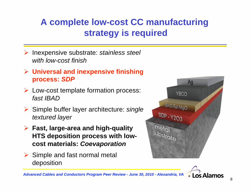
A complete low-cost CC manufacturing strategy is required
Inexpensive substrate: stainless steel
with low-cost finish
Universal and inexpensive finishing process: SDP
Low-cost template formation process: fast IBAD
Simple buffer layer architecture: single
textured layer
Fast, large-area and high-quality HTS deposition process with low-cost materials: Coevaporation
Simple and fast normal metal deposition

Advanced Cables and Conductors Program Peer Review - June 30, 2010 - Alexandria, VA 4
A process to transfer HTS materials efficiently at high rate needed: Co-evaporation
Co-evaporation of individual elements
Elemental sources inherently least expensive
Very high deposition rate can be used
Multi-hundred kW systems evaporating kg/hr exist in industry
Scalable to large deposition area
Thick film potential
Yttrium Barium Copper
Y Ba Cu

Advanced Cables and Conductors Program Peer Review - June 30, 2010 - Alexandria, VA 5
One Approach: RCE-CDR (Reactive Co-Evaporation by Cyclic Deposition and Reaction)
Stability of YBCO in the p-T diagram
O2 pocket
Deposition rate
dp ( 4Å)
Average rate
RCE-CDR
Pulsed deposition at low O2 pressure followed by reaction in high O2
Very high instantaneous deposition rates possible
Lower average rate: required for kinetics of growth
In situ growth

Advanced Cables and Conductors Program Peer Review - June 30, 2010 - Alexandria, VA 6
A Different Approach: Co-evaporation at low temperature followed by reaction at high T in O2
O2 pocket
2-step: Deposit precursor coating then process (ex situ)
R. Hammond (Stanford U), D. Christen (ORNL), and J. Storer (LANL) studied this process (2001-2006)
Several deposition methods were used
Precursor coating was stable (no fluorine) – deposited at low T and low O2 (glassy phase)
Liquid-assisted growth at high T
Very fast reaction and growth rate (>1000 Å/s)
Pinning centers hard to add; nearly defect-free
Jc’s were not consistent (some >3 MA/cm2; others 1 MA/cm2)
Liquid
TEM Section ORNL

Advanced Cables and Conductors Program Peer Review - June 30, 2010 - Alexandria, VA 7
Use IBAD-MgO templates (SuNAM fabricates templates up to 2 km in length)
SuNAM HTS growth process is fast ( 1 minute)
RCE-DR
Large deposition area
Large process margin
Typical > 250 A/cm, max ~ 500 A/cm (1.1 m)
0.6 m thick film ~ 600 m/hr.,
1.5 m thick film ~ 300 m/hr. (4 mm width equiv.)
SUNAM
An example of the 2-step process: Presently used by SuNAM in Korea
Advanced Cables and Conductors Program Peer Review - June 30, 2010 - Alexandria, VA 8
A complete low-cost CC manufacturing strategy is required
Inexpensive substrate: stainless steel
with low-cost finish
Universal and inexpensive finishing process: SDP
Low-cost template formation process: fast IBAD
Simple buffer layer architecture: single
textured layer
Fast, large-area and high-quality HTS deposition process with low-cost materials: Coevaporation
Simple and fast normal metal deposition

Advanced Cables and Conductors Program Peer Review - June 30, 2010 - Alexandria, VA 9
Solution Deposition Planarization (SDP) is a promising method for substrate finishing and eliminating defects
For more details see LANL presentation in the Strategic Research session
TEM: Terry Holesinger
Y2O3 SDP
MgO
YBCO
IBAD-MgO is extremely fast, but needs an inexpensive and fast process to produce smooth substrates for IBAD
Solution deposited layer encapsulates metal tape (prevents metal interdiffusion) and smooths out the surface
After solution deposition the substrate is IBAD-ready with an Y2O3 bed layer
Process developed by Los Alamos and Sandia National Laboratories
0
2
4
6
8
10
12
0 2 4 6 8 10
FW
HM
Mg
O T
ext
ure
(°)
RMS Roughness 5 x 5 m (nm)
in-plane alignment in MgO
out-of-plane alignment in MgO
Required RMS roughness

Advanced Cables and Conductors Program Peer Review - June 30, 2010 - Alexandria, VA 10
Solution Deposition Planarization eliminates three steps in present CC manufacturing
Current Manufacturing Process for HTS CC
Simplified SDP Process for HTS CC
Polished, expensive metal substrate
Superconductor
Barrier layer
Bed layer
IBAD
Superconductor
SDP
IBAD
SDP combines electropolishing, barrier and bed layer deposition
into one process step for IBAD CC
Additionally it broadens the range of substrates that can be used
Unpolished, inexpensive metal substrate

Advanced Cables and Conductors Program Peer Review - June 30, 2010 - Alexandria, VA 11
In FY2010 LANL built a scaled-up system for SDP
New deposition system allows for longer and wider tape coating
Previous system only allowed 3 meter coatings
New system capable of coating 100 meter lengths
Higher throughput by doing three SDP coatings in series, as well as 10-cm wide tape
Significant improvements included in the design of the new system:
Continuous flow of solution with filtering
In-line tape cleaning
Laminar air flow
Automated process control
Materials to be provided to our industrial partners
NEW SYSTEM

Advanced Cables and Conductors Program Peer Review - June 30, 2010 - Alexandria, VA 12
In FY2010 introduced multiple-molarity coatings resulting in lowest roughnesses: less than 1 nm RMS
Unpolished RMS (5x5 m): 26 nm
15-20 SDP coatings (5x5 m): 0.5 nm
Rq = 0.56 nm Ra = 0.45 nm
Rq = 25.6 nm Ra = 20.5 nm
UNPOLISHED SUBSTRATE
1
10
0 5 10 15 20 25 30
0.4 M
0.08 M
Rq (
nm
)
Number of SDP coatings
0.4 M coats
0.08 M coats
SDP-coated SUBSTRATE

Advanced Cables and Conductors Program Peer Review - June 30, 2010 - Alexandria, VA 13
High Jc achieved by Reactive Co-Evaporation on SDP-prepared substrate
YBCO deposited by LANL RCE on MgO template grown on SDP Y-Al-O
Simplified buffer structure
YBCO deposited on 30 nm MgO; Jc not yet optimized
MgO texture: = 4.6°, = 1.5°
1.0 m YBCO film
-50 0 50 100 150 200 250 300 350
Inte
nsity
Phi (degrees)
YBCO pole figure 4.1 MA/cm2, LN2, sf = 2.4°, = 0.9°
YBCO
Unpolished metal tape
SDP
Matias et al, Super. Sci. Tech., 23, 014018 (2010)
TEM Terry Holesinger
0H (T)
1
10
Jc (
MA
cm-2
)
0.1

Advanced Cables and Conductors Program Peer Review - June 30, 2010 - Alexandria, VA 14
Best RCE Critical Current Results at LANL
permanent magnets
• Best Self Field results to date:
– 3.0 MA/cm2 in a 1.2 m film
– 2.5 MA/cm2 in a 2.0 m film
– 950 A/cm-width in 6 m
– 4.1 MA/cm2 in 1.0 m 1000 A/cm
PLD YBCO
75.5 K
YBCO thickness ( m)
RCE-CDR
New result since PR09
• Measure full 1-cm width coated conductor in magnetic field
• Scale SF result from bridge
On stainless substrate

Advanced Cables and Conductors Program Peer Review - June 30, 2010 - Alexandria, VA 15
0
0.5
1
1.5
2
0 200 400 600 800 1000
HastelloyS316LYBCOreduced YBCO
Therm
al e
xpansi
on (
%)
Temperature (°C)
HTS coatings on stainless steel substrates often exhibit delamination
Stainless steel 316L substrates studied as a substrate for CC
Have obtained some good (high Ic) results
Very often, however, the YBCO films delaminate
Proposed mechanism is buckling-driven delamination under compressive stress from thermal expansion differences between S316L and YBCO
Delaminated YBCO/Ag coating
> 0.5 %

Advanced Cables and Conductors Program Peer Review - June 30, 2010 - Alexandria, VA 16
Several approaches to obtain 1000 A/cm in Coated Conductors
1000 A/cm
LANL PLD results PR09
Conventional approach is to attain higher currents by making thicker films: 5–10 m HTS films have been shown by several methods to yield close to 1000 A/cm
A harder way is to increase Jc in thicker films
Demonstrated at LANL by PLD: 2 m, 5 MA/cm2
Not easy; perhaps also not practical in manufacturing
A third way is to double the 500 A/cm film
Much easier to achieve 500 A/cm in 2-3 m
Reset the crystalline structure with a second IBAD layer and then grow a second HTS layer
SDP/IBAD YBCO1
YBCO2
SDP/IBAD
2x

Advanced Cables and Conductors Program Peer Review - June 30, 2010 - Alexandria, VA 17
YBCO
YBCO
SDP allows for ‘Stacked’ Coated Conductor layer structure with multiple SDP/IBAD/HTS layers
Je in a Coated Conductor is dominated
by the thickness of the substrate
Thus, doubling Ic effectively doubles Je
SDP enables one to grow a second
YBCO layer on top of a YBCO layer
SDP allows for stacks of HTS layers on
both sides of the metal tape
Can increase Ic and Je several fold by
using the same coating process used
for one HTS layer repeatedly on the CC
Of particular interest in applications
requiring high Je
METAL TAPE
SDP/IBAD YBCO
YBCO
YBCO SDP/IBAD
METAL SUBSTRATE

Advanced Cables and Conductors Program Peer Review - June 30, 2010 - Alexandria, VA 18
2-Layer HTS Stack preliminary result demonstrates feasibility: 700 A
SDP1: 1 m
YBCO1 by RCE: 2 m
pole figure: =2.7°
540 A/cm (SF value extrapolated from magnetic field measurement)
Ag/YBCO surface > 100 nm RMS roughness
SDP2: 1 m, RMS 2 nm
IBAD MgO2 deposited
pole figure =7.9°
YBCO2 by RCE: 2 m
pole figure =4.9°
185 A/cm (SF measured directly)
Total current 700 A
More work is under way
YBCO2
SDP/IBAD YBCO1
SDP/IBAD
MgO2 = 7.9°
Advanced Cables and Conductors Program Peer Review - June 30, 2010 - Alexandria, VA 19
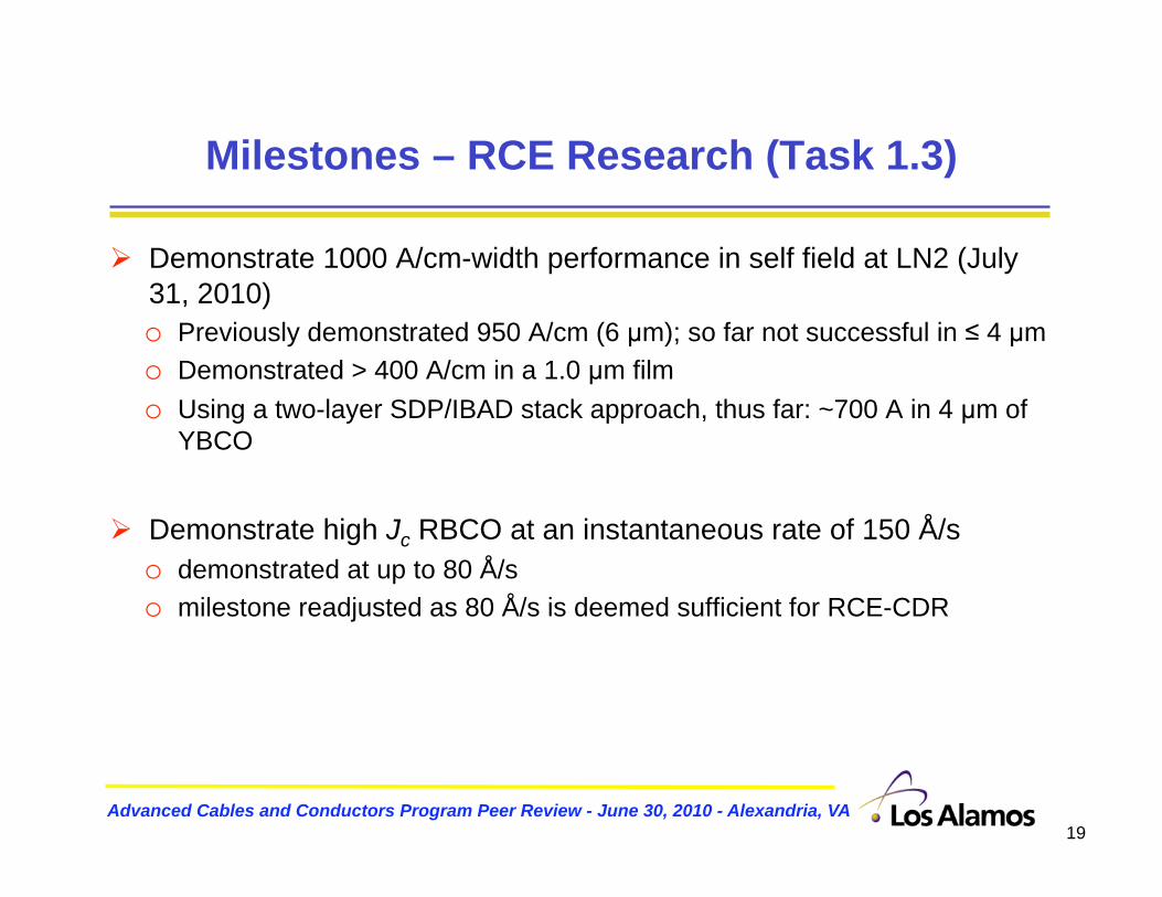
Milestones – RCE Research (Task 1.3)
Demonstrate 1000 A/cm-width performance in self field at LN2 (July 31, 2010) o Previously demonstrated 950 A/cm (6 m); so far not successful in 4 m
o Demonstrated > 400 A/cm in a 1.0 m film
o Using a two-layer SDP/IBAD stack approach, thus far: ~700 A in 4 m of YBCO
Demonstrate high Jc RBCO at an instantaneous rate of 150 Å/s
o demonstrated at up to 80 Å/s
o milestone readjusted as 80 Å/s is deemed sufficient for RCE-CDR

Advanced Cables and Conductors Program Peer Review - June 30, 2010 - Alexandria, VA 20
Technology transfer, collaborations and partnerships
Close collaboration, a number of visits and sample exchanges between LANL and Sandia on the SDP process
Numerous discussions with R. Hammond (Stanford University) regarding HTS deposition
Joint LANL/SNL R&D 100 Award Entry for SDP process
2 conference presentations (one invited talk) and 1 journal article
SDP system
R&D100

Advanced Cables and Conductors Program Peer Review - June 30, 2010 - Alexandria, VA 21
Plans for FY11
Optimize stack of YBCO layers for total Ic > 1000 A; coat both sides of substrate and several layers per side
LANL plans ot work with Stanford to explore new routes to low-cost coevaporation – (revisiting Hammond’s Path B)
Furnace
Potential for a high throughput, extremely high rate process
One pass (two-step) process

Advanced Cables and Conductors Program Peer Review - June 30, 2010 - Alexandria, VA 22
Summary
LANL demonstrated 4.1 MA/cm2, LN2 SF, in 1 m film on IBAD template by RCE-CDR
LANL introduced a new architecture using stacks of SDP/IBAD/HTS layers; first result appears promising: 700 A/cm
LANL proposes revisiting research on the 2-step co-evaporation process as a viable route to low-cost CC manufacturing