progress energy distinguished university professor jay baliga … · 2019-04-18 · process...
TRANSCRIPT

Progress Energy Distinguished University Professor Jay Baliga
April 11, 2019
1
Acknowledgements
Outline
SiC Power MOSFET Breakthroughs achieved at NCSU
PRESiCE: SiC Power Device Manufacturing Technology
SiC Power MOSFETs: Inversion Channel & Accumulation
Channel
The JBSFET: SiC MOSFET with Integrated Schottky Diode
Split-Gate (SG) MOSFET: Improved HF-FOM
Buffered-Gate (BG) MOSFET: Further Improved HF-FOM
The OCTFET: A New Cell Topology with Superior High
Frequency Figures-of-Merit
The BiDFET: A Monolithic Bi-Directional Field Effect
Transistor
2

3
Outline
SiC Power MOSFET Breakthroughs achieved at NCSU
PRESiCE: SiC Power Device Manufacturing Technology
SiC Power MOSFETs: Inversion Channel & Accumulation
Channel
The JBSFET: SiC MOSFET with Integrated Schottky Diode
Split-Gate (SG) MOSFET: Improved HF-FOM
Buffered-Gate (BG) MOSFET: Further Improved HF-FOM
The OCTFET: A New Cell Topology with Superior High
Frequency Figures-of-Merit
The BiDFET: A Monolithic Bi-Directional Field Effect
Transistor

4
SiC Power Electronic-Devices
PRESiCE: PRocess Engineered for manufacturing SiC Electronic-Devices
B.J. Baliga, et al, "PRESiCETM: Process Engineered for manufacturing SiC Electronic-Devices", Int. Conf. on Silicon Carbide and Related Materials, Paper MO.CP.10, September 18, 2017.

5
PRESiCE: PRocess Engineered for manufacturing SiC Electronic-Devices
Qualification Procedure:(1) Define Process Flow (NCSU) for Manufacturing SiC Power MOSFETs,
JBSFETs, and JBS Rectifiers at X-Fab.(2) Design a Mask Set (NCSU) for Manufacturing SiC Power MOSFETs,
JBSFETs, and JBS Rectifiers at X-Fab for Qualifying the process.(3) Fabricated Three Process Lots at X-Fab.(4) Obtained Statistical Data (NCSU) on device parameters to confirm
tight distribution of parameters from within each wafer, from wafer-to-wafer within each process lot, and from lot-to-lot.
Data Acquisition Equipment:(1) New Semi-Automated Signatone
Wafer Prober.- 6 inch wafer capability- 3 kV chuck isolation- High Temp (300 oC)
(2) New Keysight Test Equipment.- Maximum Voltage = 3 kV- Maximum Current = 20 A

Process Qualification using Three Lots at X-Fab
Device #2: JBS Rectifier with Nickel Schottky Contact
Active Area = 0.046 cm2
1.2 kV JBS Rectifier Process Qualification
6 inch SiC wafer fabricated at X-Fab
W. Sung, K. Han and B.J. Baliga, "Design and Manufacturing of 1200 V SiC JBS Diodes with Low On-State Voltage Drop and Reverse Blocking Leakage Current", Int. Conf. on Silicon Carbide and Related Materials, Paper WE.DP.9, September 20, 2017.

7
On-state Voltage Drop [V] @ If = 5A
Average = 2.00 V
Lot-3-W3-#2
Std. Dev. : 0.05
Average = 2.05 V
Lot-3-W6-#2
Std. Dev. : 0.06
JBS Rectifier with Nickel Schottky Contact (Within Lot Variation)

8
Lot-3-W3-#2 Lot-3-W6-#2
Yield : 98.7%Yield : 95.3%
Leakage Current (IL) [nA] @ Vd=1000 V, RT
Yield based on allowable maximum leakage current of 100 µA
JBS Rectifier with Nickel Schottky Contact (Within Lot Variation)

On-state Voltage Drop [V] @ if = 5A, RT
Average = 2.00 V
Lot-3-W3-#2 Lot-4-W3-#2
Average = 1.94 V
Lot-5-W3-#2
Average = 2.06 V
Std. Dev. : 0.05 Std. Dev. : 0.03 Std. Dev. : 0.07
JBS Rectifier with Nickel Schottky Contact (Lot-to-Lot Variation)

1010
Lot-5-W3-#2Lot-4-W3-#2Lot-3-W3-#2
Yield : 98.7% Yield : 96.7%Yield : 94.7%
Leakage Current (IL) [nA] @ Vd=1000 V, RT
Yield based on allowable maximum leakage current of 100 µA
JBS Rectifier with Nickel Schottky Contact (Lot-to-Lot Variation)

Process Qualification using Three Process Lots at X-Fab
Device #5: Accumulation Channel MOSFET (ACCUFET) with
JFET Implant
Active Area = 0.045 cm2
Accumulation Channel MOSFET (ACCUFET)
Technical Note:
The Rds,on values in the Wafer Maps and Statistical Data plots include 35 mΩof parasitic probe (~ 1 mΩ-cm2) and substrate (~ 1 mΩ-cm2) resistance.
The Cgd values in Wafer Maps and Statistical data include 0.5 pF of parasitic
probe capacitance.
W. Sung, K. Han and B.J. Baliga, "A Comparative Study of Channel Designs for SiC MOSFETs: Accumulation-Mode Channel vs Inversion-Mode Channel", IEEE Int. Symp. On Power Semiconductor Devices and ICs, Paper SiC-P9, pp. 375-378, June 2017, Sapporo, Japan.

12
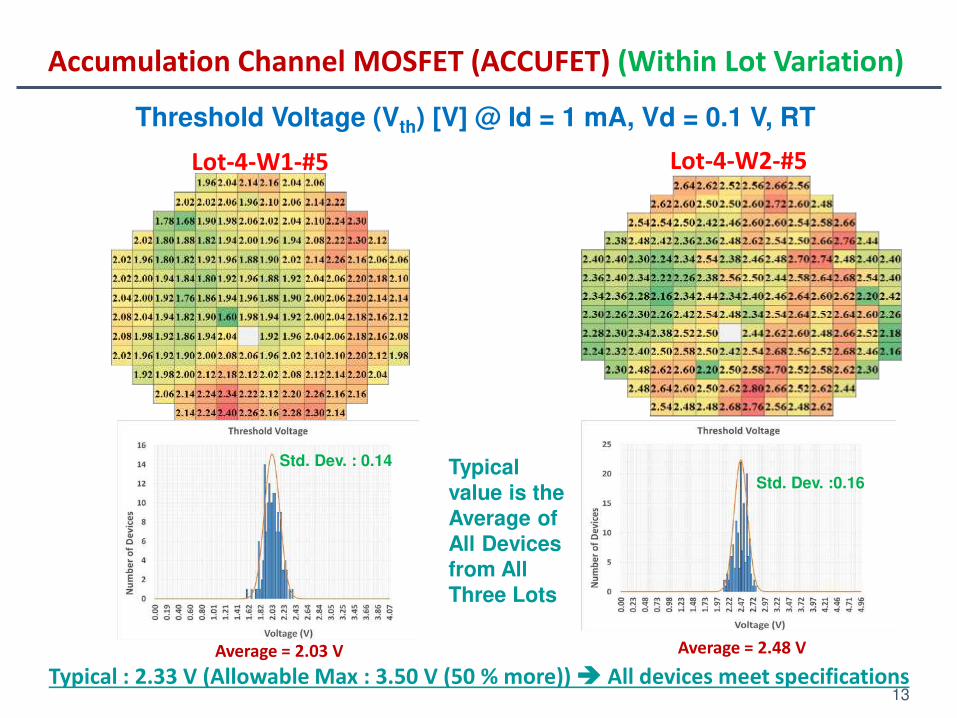
Accumulation Channel MOSFET (ACCUFET) (Within Lot Variation)
Average = 137 mΩ
Lot-4-W1-#5 Lot-4-W2-#5
Std. Dev. : 3.29
Average = 139 mΩ
On-Resistance (Ron) [mΩ] @ Id=1A, Vg=25V, RT - 6.5 mΩ-cm2
Damaged during
the BV test w/o Flourinert
Std. Dev. : 5.57
Typical: 144 mΩ (Allowable Max : 187 mΩ (30 % more)) All devices meet specifications
Typical value is the Average of All Devices from All Three Lots
13
Threshold Voltage (Vth) [V] @ Id = 1 mA, Vd = 0.1 V, RT
Lot-4-W1-#5
Average = 2.03 V
Lot-4-W2-#5
Average = 2.48 V
Std. Dev. : 0.14
Std. Dev. :0.16
Typical : 2.33 V (Allowable Max : 3.50 V (50 % more)) All devices meet specifications
Typical value is the Average of All Devices from All Three Lots
Accumulation Channel MOSFET (ACCUFET) (Within Lot Variation)
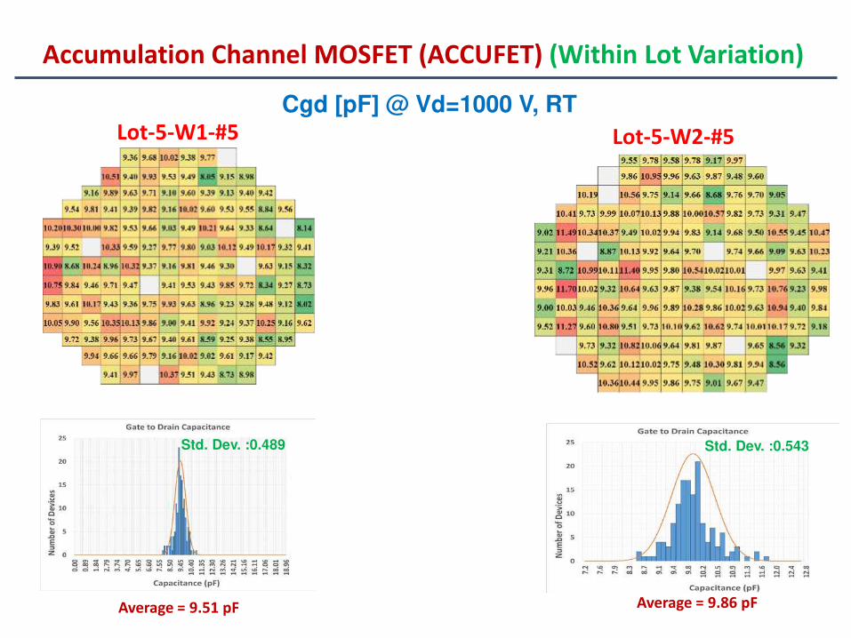
Lot-5-W1-#5
Std. Dev. :0.489
Average = 9.51 pF
Lot-5-W2-#5
Average = 9.86 pF
Std. Dev. :0.543
Cgd [pF] @ Vd=1000 V, RT
Accumulation Channel MOSFET (ACCUFET) (Within Lot Variation)

15
Leakage Current (IL) [nA] @ Vd=1000 V, RT
Lot-4-W1-#5
Yield : 95.3%
Lot-4-W2-#5
Yield : 92.7%
Yield based on allowable maximum leakage current of 100 µA
Accumulation Channel MOSFET (ACCUFET) (Within Lot Variation)

16
Lot-3-W1-#5
Average = 149 mΩ
On-Resistance (Ron) [mΩ] @ Id=1A, Vg=25V, RT
Lot-4-W1-#5
Average = 139 mΩ
Lot-5-W1-#5
Average = 150 mΩ
Std. Dev. : 2.75
Typical : 144 mΩ (Allowable Max : 187 mΩ (30 % more)) All devices meet specifications
Std. Dev. : 5.57 Std. Dev. : 3.60
Damaged during the BV test w/o Flourinert
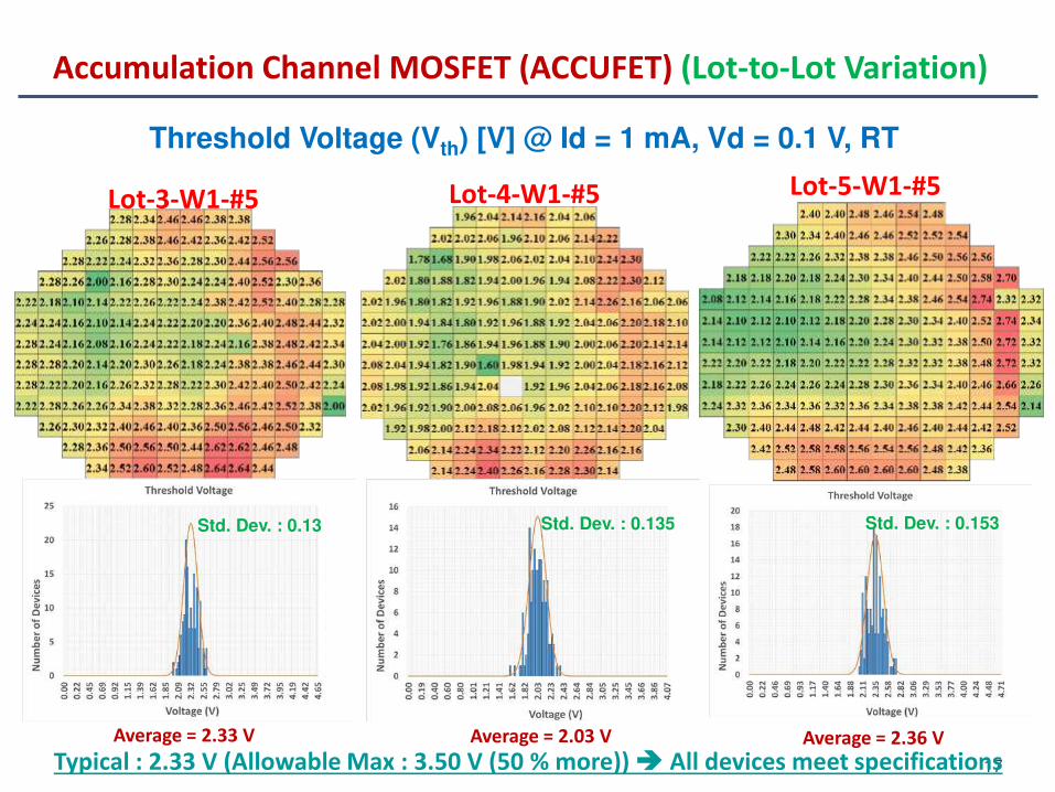
Accumulation Channel MOSFET (ACCUFET) (Lot-to-Lot Variation)
17
Lot-3-W1-#5
Threshold Voltage (Vth) [V] @ Id = 1 mA, Vd = 0.1 V, RT
Lot-4-W1-#5 Lot-5-W1-#5
Average = 2.33 V Average = 2.36 V
Std. Dev. : 0.153
Typical : 2.33 V (Allowable Max : 3.50 V (50 % more)) All devices meet specifications
Std. Dev. : 0.13 Std. Dev. : 0.135
Accumulation Channel MOSFET (ACCUFET) (Lot-to-Lot Variation)
Average = 2.03 V

18
Lot-4-W1-#5 Lot-5-W1-#5
Average = 9.64 pF
Std. Dev. :0.49
Average = 9.51 pF
Lot-3-W1-#5
Average = 10.73 pF
Std. Dev. :0.21 Std. Dev. :0.25
Damaged during the BV test w/o Flourinert
Cgd [pF] @ Vd=1000 V, RT
Accumulation Channel MOSFET (ACCUFET) (Lot-to-Lot Variation)

19
Lot-3-W1-#5 Lot-5-W1-#5Lot-4-W1-#5
Yield : 93.3 % Yield : 95.3% Yield : 96%
Leakage Current (IL) [nA] @ Vd=1000 V, RT
Yield based on allowable maximum leakage current of 100 µA
Accumulation Channel MOSFET (ACCUFET) (Lot-to-Lot Variation)
20
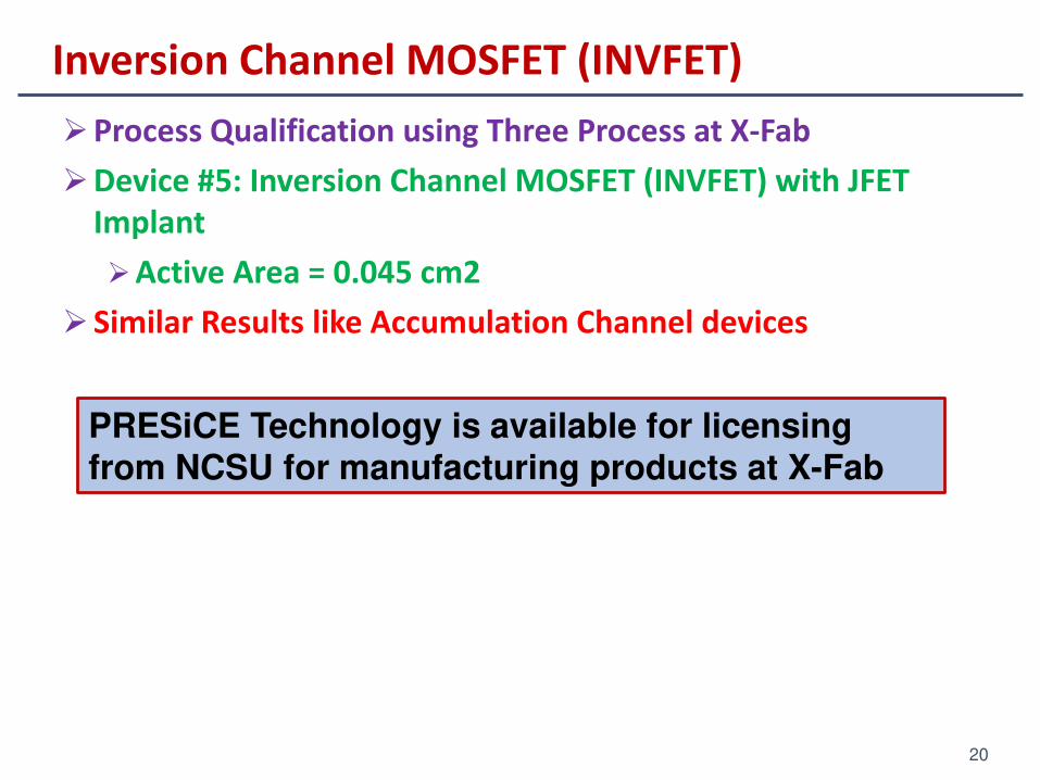
Process Qualification using Three Process at X-Fab
Device #5: Inversion Channel MOSFET (INVFET) with JFET
Implant
Active Area = 0.045 cm2
Similar Results like Accumulation Channel devices
Inversion Channel MOSFET (INVFET)
PRESiCE Technology is available for licensing from NCSU for manufacturing products at X-Fab
Outline
SiC Power MOSFET Breakthroughs achieved at NCSU
PRESiCE: SiC Power Device Manufacturing Technology
SiC Power MOSFETs: Inversion Channel & Accumulation
Channel
The JBSFET: SiC MOSFET with Integrated Schottky Diode
Split-Gate (SG) MOSFET: Improved HF-FOM
Buffered-Gate (BG) MOSFET: Further Improved HF-FOM
The OCTFET: A New Cell Topology with Superior High
Frequency Figures-of-Merit
The BiDFET: A Monolithic Bi-Directional Field Effect
Transistor
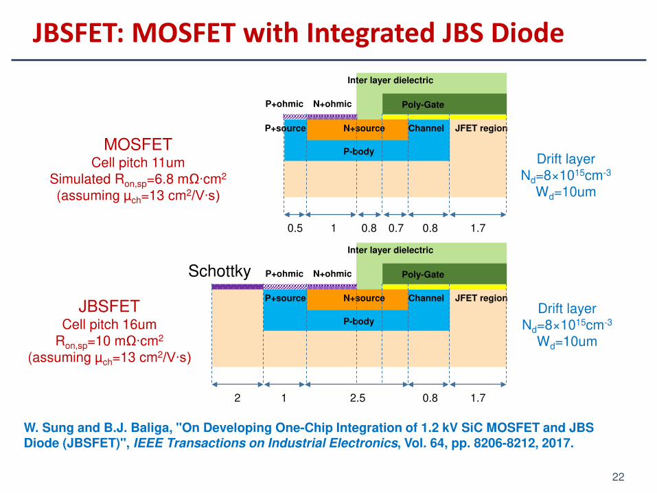
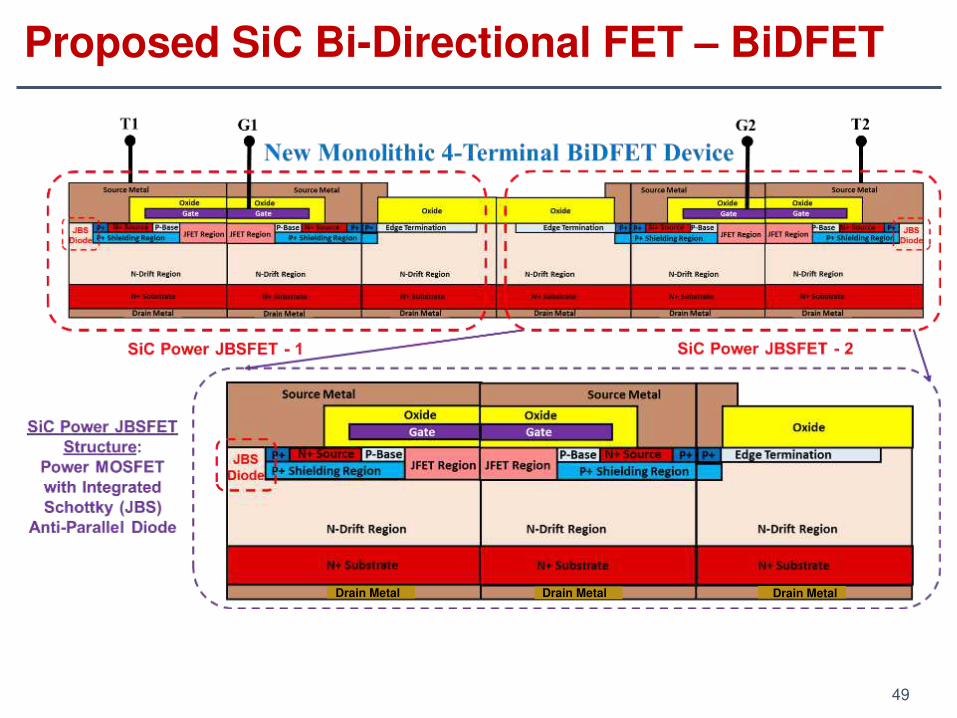
JBSFET: MOSFET with Integrated JBS Diode
22
P+ohmic N+ohmic
Inter layer dielectric
Poly-Gate
P-body
N+sourceP+source Channel JFET region
0.8 1.70.5
MOSFETCell pitch 11um
Simulated Ron,sp=6.8 mΩ∙cm2
(assuming µch=13 cm2/V∙s)
1 0.70.8
Drift layerNd=8×1015cm-3
Wd=10um
JBSFETCell pitch 16um
Ron,sp=10 mΩ∙cm2
(assuming µch=13 cm2/V∙s)
Schottky P+ohmic N+ohmic
Inter layer dielectric
Poly-Gate
P-body
N+sourceP+source Channel JFET region
2.5 0.8 1.712
Drift layerNd=8×1015cm-3
Wd=10um
W. Sung and B.J. Baliga, "On Developing One-Chip Integration of 1.2 kV SiC MOSFET and JBS Diode (JBSFET)", IEEE Transactions on Industrial Electronics, Vol. 64, pp. 8206-8212, 2017.

JBSFET Area Savings Analysis
23
Layout comparison for 1.2 kV, 5.7 A Devices
ApproachesActive area
(cm2)Edge termination
And peripheryTotal area
(cm2)
Previous approach
+0.0212 (MOSFET)
0.0263 (JBS)0.0110 (MOSFET)
0.0122 (JBS)
0.0322+0.0385 =0.0707
PA approach 1
JBSEFET10.0284
(5.72A MOSFET*)0.0126 0.041
PA approach 2
JBSFET20.0281 0.0126 0.0407
PA approach 3
JBSFET30.0475 0.016 0.0635
JBSFET
Pure MOSFET
JBSFET
Pure JBS
Pure JBS
Pure MOSFET
Assumptions:
• Edge termination design : 10 floating field rings – 3um wide, total spacing is about 20um, which gives about 50um total width for edge termination
• Periphery : Edge termination to C/S implant – 20um, dicing lane 70um per side, C/S to dicing 30um-> total 120um
• *Comparison with a 5.72A pure MOSFET : 0.0242 active + 0.0117 periphery = 0.036 cm2

24
JBSFET Area Savings Analysis
Conclusion: Area Savings of about 40 % can be achieved with the JBSFET Approach
Other Benefits: Cuts package count in half.Reduces switching loss by 40% at elevated temperatures.
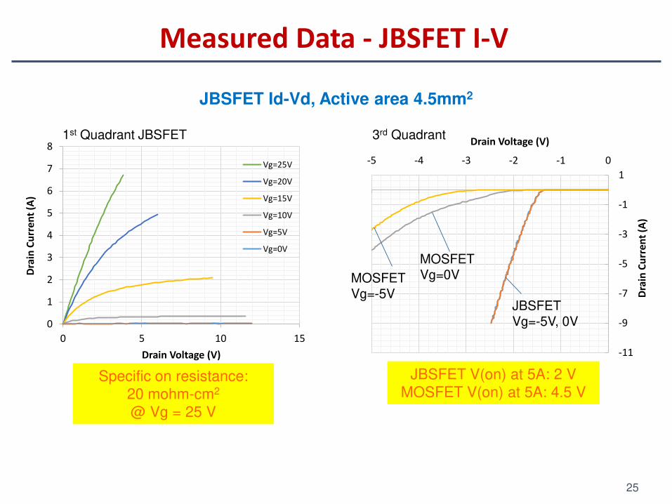
Measured Data - JBSFET I-V
25
JBSFET Id-Vd, Active area 4.5mm2
0
1
2
3
4
5
6
7
8
0 5 10 15
Dra
in C
urr
en
t (A
)
Drain Voltage (V)
Vg=25V
Vg=20V
Vg=15V
Vg=10V
Vg=5V
Vg=0V
-11
-9
-7
-5
-3
-1
1
-5 -4 -3 -2 -1 0
Dra
in C
urr
en
t (A
)
Drain Voltage (V)
JBSFETVg=-5V, 0V
MOSFETVg=-5V
MOSFETVg=0V
1st Quadrant JBSFET 3rd Quadrant
Specific on resistance:
20 mohm-cm2
@ Vg = 25 V
JBSFET V(on) at 5A: 2 V
MOSFET V(on) at 5A: 4.5 V

2626
Process Qualification using Three Process Lots at X-Fab
Device #7: Accumulation Channel JBSFET with JFET Implant
Active Area = 0.045 cm2
Accumulation Channel JBSFET
Schottky P+ohmic N+ohmic
Inter layer dielectric
Poly-Gate
P-body
N+sourceP+source Channel JFET region
2.5 0.8 1.712
Technical Note:
The Rds,on values in the Wafer Maps and Statistical Data plots include 35 mΩof parasitic probe (~ 1 mΩ-cm2) and substrate (~ 1 mΩ-cm2) resistance.
The Cgd values in Wafer Maps and Statistical data include 0.5 pF of parasitic
probe capacitance.
W. Sung and B.J. Baliga, "Monolithically Integrated 4H-SiC MOSFET and JBS Diode (JBSFET) using a Single Ohmic/SchottkyProcess Scheme", IEEE Electron Device Letters, Vol. 37, pp. 1605-1608, 2016.

27
Accumulation Channel JBSFET (Lot-to-Lot Variation)
Lot-3-W3-#7
Average = 250 mΩ
Lot-4-W3-#7
Average = 232 mΩ
Lot-5-W3-#7
Average = 268 mΩ
On-Resistance (Ron) [mΩ] @ Id=1A, Vg=25V, RT – 11 mΩ-cm2
Typical : 250 mΩ (Allowable Max : 325 mΩ (30 % more)) All devices meet specifications
Std. Dev. : 11.73 Std. Dev. : 16.6Std. Dev. : 7.05

28
Lot-3-W3-#7 Lot-4-W3-#7 Lot-5-W3-#7
Average = 2.43 V Average = 2.31 V
Std. Dev. : 0.11 Std. Dev. : 0.11Std. Dev. : 0.10
Threshold Voltage (Vth) [V] @ Id = 1 mA, Vd = 0.1 V, RT
Typical : 2.41 V (Allowable Max : 3.62 V (50 % more)) All devices meet specifications
Average = 2.50 V
Accumulation Channel JBSFET (Lot-to-Lot Variation)

29
Lot-3-W3-#7 Lot-4-W3-#7 Lot-5-W3-#7
3rd Quadrant (Vf) [V]@ If = 5A, RT
Average = 2.21 VAverage = 2.25 V Average = 2.33 V
Std. Dev. : 0.032Std. Dev. : 0.048 Std. Dev. : 0.072
Accumulation Channel JBSFET (Lot-to-Lot Variation)
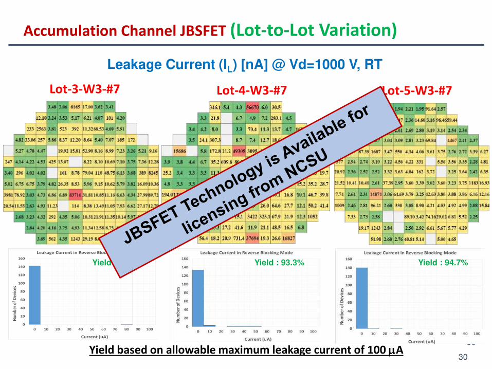
30
30
Lot-3-W3-#7 Lot-4-W3-#7 Lot-5-W3-#7
Yield : 95.3% Yield : 94.7%Yield : 93.3%
Leakage Current (IL) [nA] @ Vd=1000 V, RT
Yield based on allowable maximum leakage current of 100 µA
Accumulation Channel JBSFET (Lot-to-Lot Variation)
31
Outline
SiC Power MOSFET Breakthroughs achieved at NCSU
PRESiCE: SiC Power Device Manufacturing Technology
SiC Power MOSFETs: Inversion Channel & Accumulation
Channel
The JBSFET: SiC MOSFET with Integrated Schottky Diode
Split-Gate (SG) MOSFET: Improved HF-FOM
Buffered-Gate (BG) MOSFET: Further Improved HF-FOM
The OCTFET: A New Cell Topology with Superior High
Frequency Figures-of-Merit
The BiDFET: A Monolithic Bi-Directional Field Effect
Transistor

32
Split-Gate (SG) SiC Power MOSFET
Conventional Split-Gate
The Split-Gate SiC Power MOSFET can be fabricated with the same process as used for the Conventional MOSFET.
Gate Design is different during device layout.

33
Split-Gate (SG) SiC Power MOSFET
Conventional MOSFET
Optimum X is 0.3 µm based on alignment tolerances

34
Split-Gate (SG) SiC Power MOSFET: Experimental Results
Cgd

35
TABLE I
SUMMARY OF EXPERIMENTAL RESULTS
FOR CONVENTIONAL MOSFET AND SG-MOSFET
MOSFET SG-MOSFET
Breakdown voltage [V] 1634 1626
Threshold voltage [V] 2.00 2.08
Ron,sp [mΩ-cm2] 6.35 6.30
Cgd,sp [pF/cm2] (@Vd=0V) 15890 2620
Cgd,sp [pF/cm2] (@Vd=1kV) 110 82
Qgd,sp [nC/cm2] 351 149
FOM <R×C (@Vd=0V)> [mΩ-pF] 100890 16520
FOM <R×C (@Vd=1kV)> [mΩ-pF] 766 589
FOM <R×Q> [mΩ-nC] 2230 938
2.4x Improvement
1.3x Improvement
Split-Gate (SG) SiC Power MOSFET: Experimental Results
K. Han, B.J. Baliga, and W. Sung, "Split-Gate 1.2 kV 4H-SiC MOSFET: Analysis and Experimental Validation", IEEE Electron Device Letters, Vol. 38, pp. 1437-1440, October 2017.

36
Outline
SiC Power MOSFET Breakthroughs achieved at NCSU
PRESiCE: SiC Power Device Manufacturing Technology
SiC Power MOSFETs: Inversion Channel & Accumulation
Channel
The JBSFET: SiC MOSFET with Integrated Schottky Diode
Split-Gate (SG) MOSFET: Improved HF-FOM
Buffered-Gate (BG) MOSFET: Further Improved HF-FOM
The OCTFET: A New Cell Topology with Superior High
Frequency Figures-of-Merit
The BiDFET: A Monolithic Bi-Directional Field Effect
Transistor

37
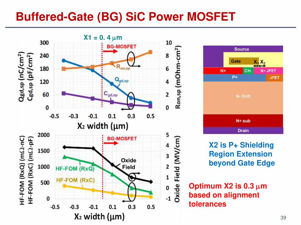
Buffered-Gate (BG) SiC Power MOSFET
Conventional Split-Gate Buffered-Gate
The Buffered-Gate SiC Power MOSFET can be fabricated with one additional (N+ JFET) Step compared with the Conventional MOSFET.
Gate Design is different during device layout.

38
0
2
4
6
8
10
12
0
4
8
12
16
20
24
0 2E+17 4E+17 6E+17 8E+17 1E+18
Oxid
e F
ield
(M
V/c
m)
Ro
n,s
p(m
Oh
m-c
m2)
Doping concentration (cm-3)
Inv. BG-MOSFET
Accu. BG-MOSFET
X1 = 0.4 µm, X2 = 0.1 µm
Optimum
Buffered-Gate (BG) SiC Power MOSFET
Optimization of N+ JFET Doping Concentration3E17 cm-3 is Optimum to: Reduce Specific On-Resistance Maintain Low Gate Oxide Electric Field
39
Buffered-Gate (BG) SiC Power MOSFET
X2 is P+ Shielding Region Extension beyond Gate Edge
X1 = 0. 4 µm
Optimum X2 is 0.3 µm based on alignment tolerances

40
Buffered-Gate (BG) SiC Power MOSFET: Experimental Results

41
Buffered-Gate (BG) SiC Power MOSFET: Experimental Results
TABLE I
SUMMARY OF EXPERIMENTAL RESULTS
FOR C-MOSFET, SG-MOSFET, AND BG-MOSFETS
C-
MOSFET
SG-
MOSFET
BG-
MOSFET_L
BG-
MOSFET_H
Cell pitch [µm] 5.6 5.6 7.0 7.0
BV [V] 1689 1688 1623 1617
Vth [V] 1.84 1.80 1.72 2.04
Ron,sp [mΩ-cm2] 5.78 5.96 10.73 8.39
Cgd,sp [pF/cm2] 121 68 21 23
Qgd,sp [nC/cm2] 347 216 56 60
FOM <Ron×Cgd>
[mΩ-pF] 698 406 229 194
FOM <Ron×Qgd>
[mΩ-nC] 2006 1287 596 503
4.0x Improvement
3.6x Improvement
K. Han, B.J. Baliga, and W. Sung, "A Novel 1.2 kV 4H-SiC Buffered-Gate (BG) MOSFET: Analysis and Experimental Validation", IEEE Electron Device Letters, Vol. 39, pp. 248-251, February 2018.

42
Outline
SiC Power MOSFET Breakthroughs achieved at NCSU
PRESiCE: SiC Power Device Manufacturing Technology
SiC Power MOSFETs: Inversion Channel & Accumulation
Channel
The JBSFET: SiC MOSFET with Integrated Schottky Diode
Split-Gate (SG) MOSFET: Improved HF-FOM
Buffered-Gate (BG) MOSFET: Further Improved HF-FOM
The OCTFET: A New Cell Topology with Superior High
Frequency Figures-of-Merit
The BiDFET: A Monolithic Bi-Directional Field Effect
Transistor
43
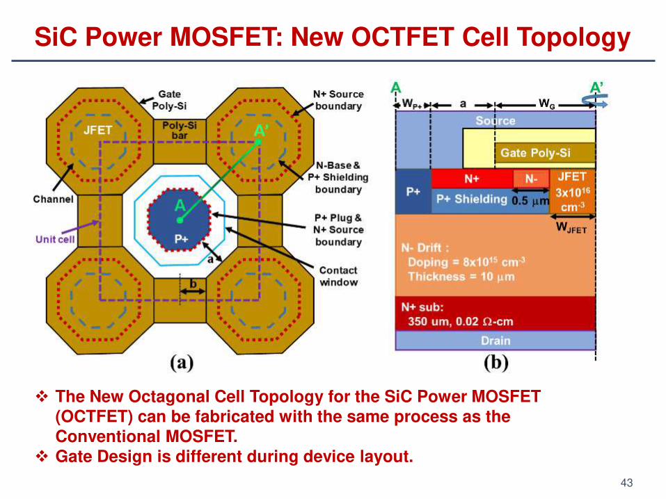
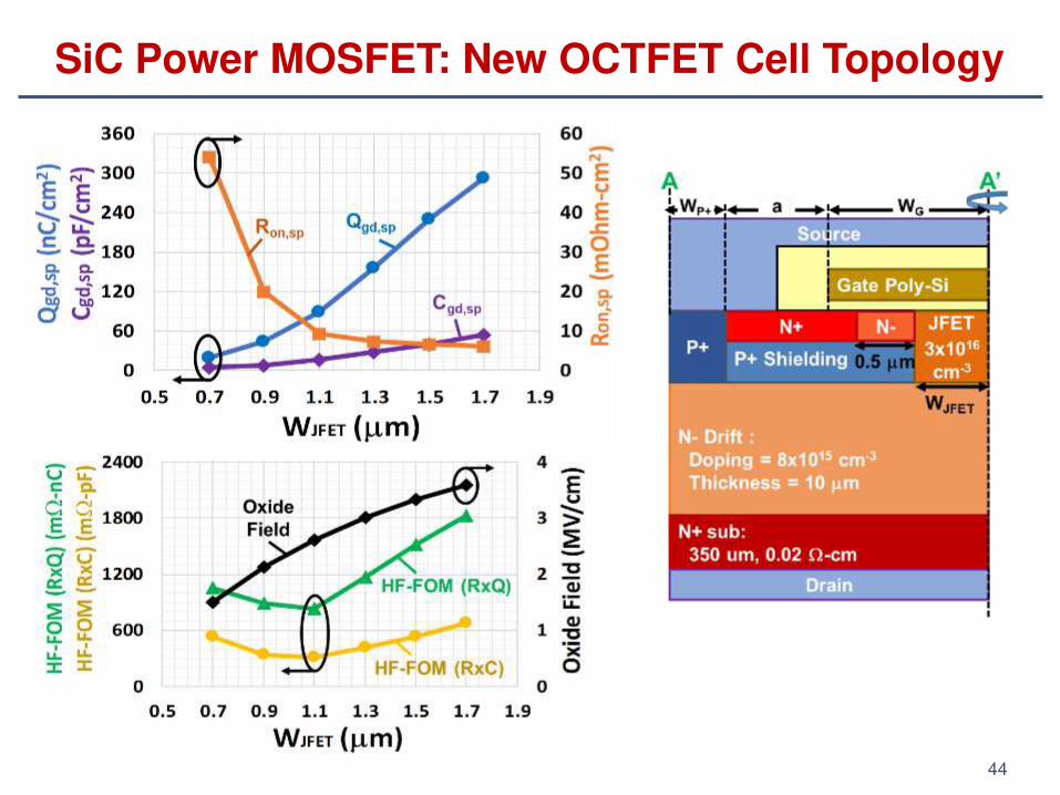
SiC Power MOSFET: New OCTFET Cell Topology
Conventional Split-Gate Buffered-Gate
The New Octagonal Cell Topology for the SiC Power MOSFET (OCTFET) can be fabricated with the same process as the Conventional MOSFET.
Gate Design is different during device layout.
44
SiC Power MOSFET: New OCTFET Cell Topology

1.2kV SiC Power OCTFET: Experimental ResultsMeasured Performance of Devices fabricated at X-Fab Foundry
45

46
SiC Power MOSFET: New OCTFET Cell Topology
TABLE I
SUMMARY OF EXPERIMENTAL RESULTS
FOR THE OCTFETS AND THE CONVENTIONAL LINEAR MOSFET
linear_J0.7 O_J0.9 O_J1.1 O_J1.3 O_J1.5 O_J1.1_C CH. density
[µm-1] 0.357 0.258 0.259 0.258 0.256 0.377
JFET density 0.250 0.075 0.098 0.121 0.144 0.143
BV [V] 1628 1639 1605 1630 1607 1605
Vth [V] 1.96 2.04 2.02 2.06 2.12 2.12
*Ron,sp [mΩ-cm2] 5.61 25.52 12.82 9.72 8.38 8.47
Cgd,sp [pF/cm2] 106 21 28 53 72 34
Qgd,sp [nC/cm2] 311 67 113 160 233 144
FOM (Ron×Cgd) [mΩ-pF] 595 536 359 515 603 288
FOM (Ron×Qgd) [mΩ-nC] 1745 1710 1449 1555 1953 1220
* includes Rsub (~0.7 mΩ-cm2)
1.4x Improvement
2.1x Improvement
K. Han and B.J. Baliga, “The 1.2 kV 4H-SiC OCTFET: A New Cell Topology with Improved High-Frequency Figures-of-Merit", IEEE Electron Device Letters, Vol. 40, pp. 299-302, February 2019.

47
Outline
SiC Power MOSFET Breakthroughs achieved at NCSU
PRESiCE: SiC Power Device Manufacturing Technology
SiC Power MOSFETs: Inversion Channel & Accumulation
Channel
The JBSFET: SiC MOSFET with Integrated Schottky Diode
Split-Gate (SG) MOSFET: Improved HF-FOM
Buffered-Gate (BG) MOSFET: Further Improved HF-FOM
The OCTFET: A New Cell Topology with Superior High
Frequency Figures-of-Merit
The BiDFET: A Monolithic Bi-Directional Field Effect
Transistor

48
BiDFET: Monolithic Bi-Directional FET
49
Proposed SiC Bi-Directional FET – BiDFET
Drain Metal Drain Metal Drain Metal

50
BiDFET: Experimental Results

51
BiDFET: Experimental Results
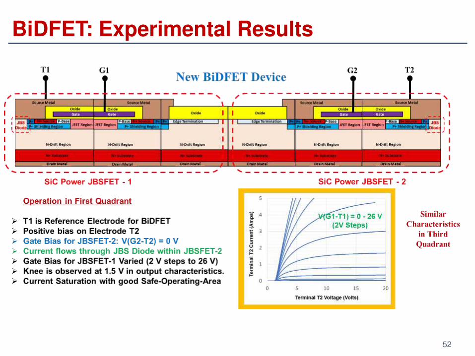
52
BiDFET: Experimental Results

53
BiDFET: Comparison with Prior Art
Assumptions: Si Diode On-State Voltage Drop = 1.5 V Si Asymmetric IGBT On-State Voltage Drop = 2.0 V Si Symmetric (RB) IGBT On-State Voltage Drop = 2.5 V SiC Diode On-State Voltage Drop = 1.5 V SiC MOSFET On-State Voltage Drop = 0.25 V

54
BiDFET: Monolithic Bi-Directional FET
B.J. Baliga and K. Han, "Monolithic SiC Bi-Directional Field Effect Transistor (BiDFET): Concept, Implementation, and Electrical Characteristics ", GOMACTech 2018, Paper 3.2, pp. 32-35, March 13, 2018.

55
Conclusion
SiC Power MOSFET Breakthroughs achieved at NCSU
PRESiCE: SiC Power Device Manufacturing Technology
SiC Power MOSFETs: Inversion Channel & Accumulation
Channel
The JBSFET: SiC MOSFET with Integrated Schottky Diode
Split-Gate (SG) MOSFET: Improved HF-FOM
Buffered-Gate (BG) MOSFET: Further Improved HF-FOM
The OCTFET: A New Cell Topology with Superior High
Frequency Figures-of-Merit
The BiDFET: A Monolithic Bi-Directional Field Effect
Transistor