programme essderc sponsors - yuminaka lab.133.8.16.23/analog/essderc_esscirc_programme.pdf ·...
TRANSCRIPT
P R O G R A M M E E S S D E R C
www.essderc2005 .com
35th European Solid-State Device Research Conference12 - 16 September 2005 - Grenoble, France
Organized by
Technical Co-Sponsorship
CNRS-INPG-UJF
SPONSORSThank you to our generous sponsors:
Soitec
SAMSUNG ADVANCEDINSTITUTE OF TECHNOLOGY
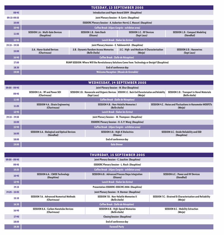
TUESDAY, 13 SEPTEMBER 200508:45
Coffee Break (Alpes Congrès - exhibtion area)
SESSION 1.A. : Multi-Gate Devices (Dauphine)
Introduction and Paper Award 2004 (Dauphine)
11:05
09:15-09:55 Joint Plenary Session - R. Cavin (Dauphine)
10:00 ESSDERC Plenary Session - A. Auberton-Hervé, C. Mazuré (Dauphine)
10:40
SESSION 1.B. : Gate Stack (Oisans)
SESSION 1.C. : RF Devices (Sept Laux)
SESSION 1.D. : Compact Modeling (Stendhal)
Lunch Break (Salon les Ecrins)
14:15 - 14:55
12:45
Joint Plenary Session - E. Yablonovitch (Dauphine)
2.A. : Nano-Scaled Devices(Chartreuse)15:00 2.B. : Dynamic Random Access Memories
(Belle Etoile)2.C. : High- and Medium-K Characterisation
(Meije)SESSION 2.D. : Nanowires
(Sept Laux)
Coffee Break (Salle de Réception)
17:00
16:40
RUMP SESSION: Where Will the Revolutionary Solutions Come from: Technology or Design? (Dauphine)
18:30 End of conference day
Welcome Reception (Musée de Grenoble)19:00
WEDNESDAY, 14 SEPTEMBER 200509:00 - 09:40
Coffee Break (Salle de Réception)
SESSION 4.A. : Strain Engineering(Chartreuse)
Joint Plenary Session - M. Shur (Dauphine)
11:25
11:05
18:00 End of conference day
Gala Dinner19:00
SESSION 3.A. : RF and Power SOI(Chartreuse)09:45 SESSION 3.B. : Nanoscale and Organic Devices
(Sept Laux)SESSION 3.C. : Back-End Characterisation and Reliability
(Meije)SESSION 3.D. : Transport in Novel Materials
(Belle étoile)
Lunch Break (Salon les Ecrins)12:45
14:15 - 14:55 Joint Plenary Session - M. Thompson (Dauphine)
15:00 ESSDERC Plenary Session - H.-S. P. Wong (Dauphine)
Coffee Break (Alpes Congrès - exhibtion area)15:40
SESSION 5.A. : Biological and Optical Devices(Stendhal)16:00
THURSDAY, 15 SEPTEMBER 200509:00 - 09:40
Coffee Break (Alpes Congrès - exhibtion area)
SESSION 6.A. : CMOS Technology(Dauphine)
Joint Plenary Session - C. Joachim (Dauphine)
10:45
10:25
18:00 End of conference day
Farewell Party19:30
Lunch Break (Salon les Ecrins)12:45
14:15 Presentation ESSDERC-ESSCIRC 2006 (Dauphine)
14:25 - 15:05 Joint Plenary Session - H. Stormer (Dauphine)
SESSION 8.A. : Carbon Nanotube Devices(Chartreuse)16:40
09:45 ESSDERC Plenary Session - L. Risch (Dauphine)
17:40 Closing Session (Dauphine)
Coffee Break (Salle de Réception)16:30
SESSION 7.A. : Advanced Numerical Methods(Chartreuse)15:10
SESSION 4.B. : Non-Volatile Memories I(Belle étoile)
SESSION 4.C. : Noise and Fluctuations in Nanometer MOSFETs(Meije)
SESSION 5.B. : High-K Dielectrics(Oisans)
SESSION 5.C. : Oxide Reliability and ESD(Dauphine)
SESSION 6.B. : Advanced Process Steps Integration(Oisans)
SESSION 6.C. : Power and HV Devices(Stendhal)
SESSION 7.B. : Non-Volatile Memories II(Belle étoile)
SESSION 7.C. : Strained Si Characterisation and Reliability(Meije)
SESSION 8.B. : High-Speed Memories(Belle étoile)
SESSION 8.C. : Mobility Extraction(Meije)
1
The 35th European Solid-State Device Research Conference takes place inGrenoble from Tuesday 13 September to Thursday 15 September 2005. Theaim of the conference is to provide an annual European forum for thepresentation and discussion of recent advances in semiconductor devices andtechnologies. ESSDERC 2005 is jointly organized with the 31st European Solid-State Circuits Conference (ESSCIRC). The initiative to merge the two sisterconferences was started in 2002, as an incentive to foster the necessaryinteraction among technologists, device experts, and circuit & system designers.While keeping separate Technical Programme Committees, ESSDERC andESSCIRC are governed by a single Steering Committee and share plenarykeynote presentations, tutorials (September 12) and satellite workshops(September 16) bridging both communities. Participants registered for eitherconference are encouraged to attend any of the scheduled parallel sessions.
ESSDERC-ESSCIRC is the largest and best quality European meeting related tomicro and nano electronics. In order to guarantee the excellence of the scientificlevel, the Steering Committee has abolished posters and half-timepresentations, while imposing a very strict acceptance rate (40%). The evaluationof submitted papers has been improved: enlarged Technical ProgrammeCommittee, redesigned sub-committee topics, increased number of reportsper paper, new functionalities enabled in the web submission system. A totalnumber of 308 papers were submitted to ESSDERC, representing a tremendousincrease (+ 85 papers) compared to 2004 and a record for the last decade.More than 30 countries, from all continents, were represented with substantialparticipations from Europe, USA, Japan and Korea. Most of the papers originatedfrom strong national (55%) and international (16%) co-operations. Only 123contributions could be included in the final programme of ESSDERC 2005which also features outstanding plenary and session invited talks. ESSDERC'05will especially focus on advanced device concepts, revolutionary transistorarchitectures, new technologies and process steps related to ITRS road blocks,nanotechnologies, quantum and molecular devices, sensors and displays, etc.
Several innovations are tested or reintroduced this year: a joint panel session,session invited talks, an exhibit, a farewell party and technical visits (FridaySeptember 16). Our conference has a new logo. A Special Issue of Solid-StateElectronics will contain selected full-length papers. Grenoble will not miss theopportunity to preserve and develop the tradition of a warm Social Programme:the Welcome Reception at the Museum of Grenoble (Tuesday evening), theGala Dinner and Show on Wednesday evening and, finally, the Farewell Party(Thursday evening) at the scenic Bastille location which overlooks Grenoblearea and mountains. The accompanying persons will enjoy several excursions.Grenoble is a high-tech city, with wonderful surroundings in the heart of theAlps, offering attractive opportunities for an extended stay over the weekend.
We would like to thank the authors for their contributions, the members ofthe Technical Programme Committee, Steering Committee and Local OrganizingCommittee for their hard work, Mrs Iris Mazuré our omnipresent conferencesecretary, and our generous sponsors.
We are looking forward to a successful conference, with exciting scientificcontents and rich human interactions. We warmly welcome you and yourcolleagues to Grenoble.
Sorin Cristoloveanu, Conference ChairMichel Brillouët, Conference Co-ChairThomas Skotnicki, ESSDERC Technical Programme Chair
WELCOME
2
TABLE OF CONTENTS ESSDERC
CONFERENCE ORGANISATION
COMMITTEES
GENERAL INFORMATION
CONFERENCE SITE
MAP CONFERENCE FACILITIES
CONFERENCE REGISTRATION
CONFERENCE INFORMATION
SOCIAL PROGRAMME
ACCOMPANYING PERSONS PROGRAMME
ESSDERC-ESSCIRC JOINT PLENARY TALKS
ESSDERC-INVITED PLENARY TALKS
EXHIBITORS
MONDAY, 12 SEPTEMBER SHORT COURSES
TUESDAY, 13 SEPTEMBER SCIENTIFIC PROGRAMME
WEDNESDAY, 14 SEPTEMBER SCIENTIFIC PROGRAMME
THURSDAY, 15 SEPTEMBER SCIENTIFIC PROGRAMME
FRIDAY, 16 SEPTEMBER WORKSHOPS
FRIDAY, 16 SEPTEMBER TECHNICAL VISITS
page(s)
3
4 - 6
7 - 8
9 - 10
11 - 12
13 - 14
15
16
17
18
19 - 20
21 - 22
23 - 24
25 - 31
32 - 39
40 - 47
47
48
ESRF in Grenoble.
3
CONFERENCE ORGANISATIONChairs
Sorin CristoloveanuGeneral [email protected]. +33 (0) 476 85 60 40
Michel BrillouëtCo-General [email protected]. +33 (0) 438 78 43 02
Thomas SkotnickiESSDERC Technical Programme [email protected]. +33 (0) 476 92 68 29
Further information
For further information about the conference please contact the conferencesecretariat:
Iris Mazuré EspejoIMEP/ENSERG23 rue des Martyrs, BP 257,38016 Grenoble cedex 1, [email protected]. +33 (0) 476 85 60 76Fax +33 (0) 476 85 60 70
Or visit the web page: http://www.essderc2005.com
2005 mm silicon wafers.

4
Technical programme committee
G.A.J. Amaratunga Cambridge University (UK)Franck Arnaud STMicroelectronics Crolles (F)Asen Asenov University of Glasgow (UK)Peter Ashburn University of Southampton (UK)Emmanuel Augendre IMEC (B)Jean-Luc Autran Université d'Aix-Marseille (F)Giorgio Baccarani University of Bologna (I)Livio Baldi STMicroelectronics Agrate (I)Francis Balestra IMEP (F)Anton Bauer FhG, Erlangen (D)Romuald Beck Warsaw University of Technology (PL)Stefan Bengtsson Chalmers University (S)Roberto Bez STMicroelectronics Agrate (I)Josef Boeck Infineon (D)Frederic Boeuf STMicroelectronics Crolles (F)Ingo Bork Synopsys (US)Ralf Brederlow Infineon (D)Hugues Brut STMicroelectronics Crolles (F)Joachim Burghartz DIMES (NL)Eugenio Cantatore Philips Leuven (B)Alain Chantre STMicroelectronics Crolles (F)Cesare Clementi STMicroelectronics Agrate (I)Raphael Clerc IMEP (F)Philippe Coronel STMicroelectronics Crolles (F)Gilles Dambrine IEMN (F)An De Keersgieter IMEC (B)Kristin De Meyer IMEC (B)Christian De Prost Atmel (F)Barbara De Salvo CEA-LETI (F)Stefaan Decoutere IMEC (B)Simon Deleonibus CEA-LETI (F)Emmanuel Dubois IEMN (F)Ignaz Eisele Universität der Bundeswehr München (D)Olof Engström Chalmers University (SE)Thomas Ernst CEA-LETI (F)Pietro Erratico STMicroelectronics Agrate (I)Denis Flandre University Catholique de Louvain (B)Francisco Gamiz University of Granada (SP)Jacques Gautier CEA-LETI (F)Gérard Ghibaudo IMEP (F)John Grant Freescale Crolles (US)Guido Groeseneken IMEC (B)Steven Hall University of Liverpool (UK)Paul Heremans IMEC (B)Jacob Hooker Philips Leuven (B)Giuseppe Iannacconne University of Pisa (I)Adrian Ionescu EPFL (CH) - TPC Vice-Chair
COMMITTEES

5
Ryoichi Ishihara Tu Delft (NL)Kazunari Ishimaru Toshiba (JP)Hiroshi Ishiwara Tokyo Institute of Technology (JP)Hiroshi Iwai Tokyo Institute of Technology (JP)Hervé Jaouen STMicroelectronics Crolles (F)Casper Juffermans Philips Leuven (B)Malgorzata Jurczak IMEC (B)Erich Kasper University of Stuttgart (D)Steven J. Koester IBM (US)Heinrich Kurz RWTH Aachen/ AMO (D)Andrea Lacaita University of Milano (I)William Lane Analog Devices (IR)Gilles Le Blevennec CEA (F)Gilles Le Carval CEA-LETI (F)Jürgen Lorenz FhG, IISB (D)Lidia Lukasiak Warsaw University of Technology (PL)Massimo Macucci University of Pisa (I)Pascal Masson Université d'Aix-Marseille (F)Alfonso Maurelli STMicroelectronics Agrate (I)Carlos Mazuré SOITEC (F)Kevin McCarthy University College Cork (IR)Bernd Meinerzhagen TU Braunschweig (D)Robert Mertens IMEC (B)Bunji Mizuno Ultimate Junction Technology Lab, (JP)André Montree Philips Leuven (B)Judith Mueller Freescale Crolles (USA)Malgorzata Napieralski University of Technology Lodz (PL)Alexiei Nazarov University of Kiev (UA)Olivier Noblanc STMicroelectronics Crolles (F)Serguei Okhonin Innovative Silicon (CH)Mikael Östling KTH (S)Alain Poncet INSA Lyon (F)Henryk Przewlocki ITE Warsow (PL)Lothar Risch Infineon (D)Massimo Rudan University of Bologna (I)Adrian Rusu Techical University of Bucharest (Ro)Paulius Sakalas University of Technology Dresden (D),
Semiconductor Physics Institute, LithuaniaJean-Michel Sallese EPFL (CH)Enrico Sangiorgi University of Bologna (I)Marc Sanquer CEA (F)Andreas Schenk Integrated Systems Laboratory (CH)Jurriaan Schmitz University of Twente (NL)Wim Schoenmaker MAGWEL (B)Hermann Schumacher Universität Ulm (D)Siegfried Selberherr TU Wien, (A)Luca Selmi University of Udine (I)Michael Stoisiek University of Erlangen (D)Peter Stolk Philips Crolles (F)
COMMITTEES

6
Eiichi Suzuki National Institute of AdvancedIndustrial Science and Technology (JP)
Roland Thewes Infineon (D)Dimitris Tsoukalas IMEL/NCRS (GR)Mateo Valenza University of Montpellier (F)Jan Van Houdt IMEC (B)Marc Van Rossum IMEC (B)Günter Weimann (FhG / IAF Freiburg (D)Terence Whall Warwick University (UK)Andreas Wild Freescale (USA)Hans-Dieter Wohlmuth Infineon (D)Reinout Woltjer Philips Leuven (NL)Jason Woo UCLA (US)Katsunobu Yoshimura NEC Electronics Corporation (JP)Bin Yu NASA (US)Alex Zaslavsky Brown University (USA)
ESSDERC-ESSCIRC Steering committee
Werner Weber (Chair) Infineon Corporate Research (D)Giorgio Baccarani (Vice-Chair) University of Bologna (I)Peter Ashburn University of Southampton (UK)Cor Claeys IMEC (B)Sorin Cristoloveanu IMEP (F)Franz Dielacher Infineon Technologies Austria (A)Christian Enz CSEM (CH)José Epifanio da Franca Chipidea Microelectrónica (POR)Ernesto Perea STMicroelectronics (F)Hans-Jörg Pfleiderer University of Ulm (D)William Redman-White Philips Semiconductors (UK)Christer Svensson University of Lingköping (S)Reinout Woltjer Philips Research (NL)
ESSDERC-ESSCIRC Local organising committee
Raphaël Clerc IMEP-INPG (F)Simon Deleonibus CEA LETI (F)Denis Duret CEA LETI (F)Laurent Fesquet TIMA - INPG (F)Gérard Ghibaudo IMEP - INPG (F)Jalal Jomaah IMEP - INPG (F)Laurent Montes IMEP - INPG (F)Mehdi Moussavi CEA LETI (F)Frédéric Petrot TIMA/SLS - INPG (F)Marc Renaudin TIMA - INPG (F)Thomas Repellin AEPI (F)Patrice Senn France Telecom R&D (F)Gilles Sicard TIMA - INPG (F)
COMMITTEES
7
GRENOBLE - An Attractive DestinationGrenoble is the capital of the French Alpes, located in a valley surrounded bybeautiful mountains. On the touristic side, Grenoble is famous for alpinelandscapes, sunshine and snow. Stendhal once wrote that “...there was amountain at the end of each Grenoble street: Belledonne, Vercors andChartreuse...”
On the scientific side, Grenoble is often referred to as the place where theSilicon and SOI Valleys merge. Stendhal would certainly write today that“…there is research lab or high-tech place at the corner of each mountain”.
A number of advanced R&D centres and leading semiconductor fabs arescattered around Grenoble. Application oriented research is blooming, itsroots being the dense network of laboratories dedicated to basic research.World class institutes (European Synchrotron Radiation Facility, CEA, CNRS,High Magnetic Field Laboratory, Neutron ILL reactor, etc) are surrounded bynumerous smaller, yet outstanding University and CNRS laboratories.
Grenoble is one of the major university towns in France: over 60 000 studentsrepresenting about 10% of the population of the greater Grenoble area.Grenoble is understandably proud of its academic and scientific environment,with a long tradition of partnership between research and industry.
ClimateSeptember is usually a sunny month with an average temperature of 20 - 24°C.Since rain showers are possible, light clothing and a raincoat are recommended.However, the organisers have negotiated perfect weather conditions...
Time ZoneCentral European summer time (GMT + 2).
ElectricityStandard European type 2 pin round sockets with 220 Volts, 50Hz are used.
Currency and Value Added Tax (VAT)The French national currency is the Euro. France has a Value Added Tax calledT.V.A (19.6 %) that is included in the price of all goods and services. Visitorsare entitled to claim this tax back on purchases made over a certain amount,upon or after leaving the country.
Tips
Tips in restaurants, hotels and taxis are not usual; they are included in the cost.
GENERAL INFORMATION

8
Banks
Banks are usually open from Monday to Friday from 09h00-16h00. Some banksare closed on Monday and some are open on Saturday.
Emergency calls
In case of emergency, dial 18 for Fire/accident and 15 for Medical Help (SAMU).
Visa Requirements
All foreign participants must have a valid passport, except the European Unioncitizens, who need only an identification card. According to the citizenship,the duration and purpose of the stay in France, a visa may be required.For more information http://www.diplomatie.fr/venir/visas/
Invitation letters to apply for a visa will be sent by the organisers upon request.We advise you to forward your request before 15 July 2005 to:
clearly indicating the dates of arrival and departure.
Hotel Reservation
ESSDERC-ESSCIRC'05 has blocked hotel rooms for the participants until August1, 2005. Please note that September is high season for business travellers. Itis therefore strongly recommended to complete the reservation of your hotelroom as soon as possible.
An updated hotel list is available on:
http://www.essderc2005.com or http://www.esscirc2005.com
Please contact the hotel of your choice and make the reservation directly,mentioning the name of the conference.
GENERAL INFORMATION

9
Gare SNCF
Mairie
CentreCommercial
Patinoire
ALPEXPOsortie n° 6
Rocade Sud
Av. Edmond Esmonin
Avenue Jean Perrot
Av. de L’Europe
Avenue Marcellin Berthelot
Boulevard Jean Pain
Av. Marie Raynoard
Rue Paul Verlaine
LyonParis
La Bastille
Téléphérique
GenèveChambèry
L’Isère
L’Isère
Le D
rac
SisteronMarseille
Auto
rout
e A4
80
Tram ligne A
Tram ligne B
Cour
s de
La L
ibér
atio
n et
du
Géné
ral D
e Ga
ulle
Tram ligne A
ALPES CONGRES
ALPEXPO
Av. d’Innsbruck
Rue Henri Barbusse
Rue Le Corbusier
Av. R
. Cha
nas
Downtown
Le D
rac
The conferences will be held at:
How to get to the conference site
From downtown / Grenoble train station:
y Tramway line A, direction Echirolles : Denis Papin, Stop : Pôle Sud.
y By car:Take Rocade Sud (coming from A48 Lyon-Grenoble or A41 Genève-Chambery-Grenoble), exit number 6: Alpexpo-Grand Place. There is alarge car park in front of the Alpes Congrès - Alpexpo conference centre.
CONFERENCE SITE
Alpes Congres - AlpexpoAvenue d’Innsbruck - BP 2408
38034 GRENOBLE - France
Tel. +33 (0) 476 39 66 00
10
By plane:
y Lyon-St. Exupéry airport www.lyon.aeroport.fr : 1 hour drive.Taxi cost : approx. 130 - 140 EUR - Tel. + 33 (0) 826 800 826.
y Airport shuttle bus SATOBUS www.satobus.com (every hourhh.30 from 7.30 am to 21.30 pm direction Grenoble, every hourhh.00 from 5.00 am to 20.00 pm direction Lyon-St. Exupéry) -Tel. + 33 (0) 472 68 72 17
y Airport Genève-Cointrin www.gva.ch : 1.5 - 2 hours drive.Taxi costs : approx. 220 EUR - Tel. + 41 (0) 22 798 20 00
By train:
y High Speed Train (TGV)Grenoble-Paris 3 hours - 7 trains every day(other TGV from Lille, Nantes)
Grenoble Gare SNCF :Tel. + 33 (0)8.92.35.35.35. (reservations) - www.sncf.fr
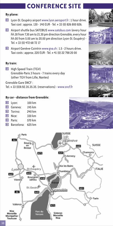
By car - distance from Grenoble:
y Lyon: 100 kmy Geneva: 145 kmy Torino: 240 kmy Nice: 330 kmy Paris: 570 kmy Barcelona: 625 km
CONFERENCE SITE

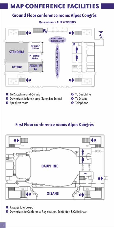
MAP CONFERENCE FACILITIES
11
Alpes Congres and Alpexpo are connected by an inner passage.
First Floor conference rooms Alpexpo
BELLE-ETOILE
SEPTLAUX
CHARTREUSE
MEIJE
LESBANS
SALLE DE RECEPTION(Coffee Break)
EntranceALPEXPO
Passage toconference rooms
ALPES CONGRES
Passage to conference roomsALPES CONGRES
PELVOUX
12
MAP CONFERENCE FACILITIESGround Floor conference rooms Alpes Congrès
STENDHAL
LESDIGUIERES
INTERNETAREA
BERLIOZ(Office)
BAYARD
To Dauphine and Oisans To Dauphine Downstairs to lunch area (Salon Les Ecrins) To Oisans Speakers room Telephone
CONFERENCEREGISTRATION
Main entrance ALPES CONGRES
EXHI
BITI
ON
AN
D Co
ffee
BRE
AKS
First Floor conference rooms Alpes Congrès
DAUPHINE
Bar
OISANS
Passage to Alpexpo Downstairs to Conference Registration, Exhibition & Coffe Break
13
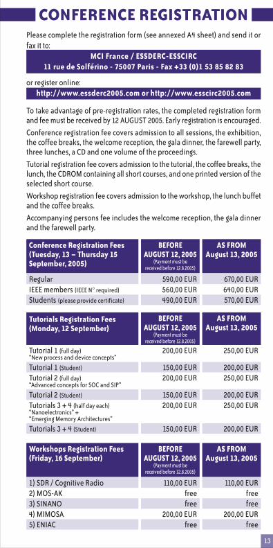
Please complete the registration form (see annexed A4 sheet) and send it orfax it to:
MCI France / ESSDERC-ESSCIRC11 rue de Solférino - 75007 Paris - Fax +33 (0)1 53 85 82 83
or register online:http://www.essderc2005.com or http://www.esscirc2005.com
To take advantage of pre-registration rates, the completed registration formand fee must be received by 12 AUGUST 2005. Early registration is encouraged.Conference registration fee covers admission to all sessions, the exhibition,the coffee breaks, the welcome reception, the gala dinner, the farewell party,three lunches, a CD and one volume of the proceedings.Tutorial registration fee covers admission to the tutorial, the coffee breaks, thelunch, the CDROM containing all short courses, and one printed version of theselected short course.Workshop registration fee covers admission to the workshop, the lunch buffetand the coffee breaks.Accompanying persons fee includes the welcome reception, the gala dinnerand the farewell party.
CONFERENCE REGISTRATION
Conference Registration Fees(Tuesday, 13 – Thursday 15September, 2005)
BEFOREAUGUST 12, 2005
(Payment must bereceived before 12.8.2005)
AS FROMAugust 13, 2005
RegularIEEE members (IEEE N° required)
Students (please provide certificate)
590,00 EUR560,00 EUR490,00 EUR
670,00 EUR640,00 EUR570,00 EUR
Tutorials Registration Fees(Monday, 12 September)
Tutorial 1 (full day)“New process and device concepts”
Tutorial 1 (Student)
Tutorial 2 (full day)“Advanced concepts for SOC and SIP”
Tutorial 2 (Student)
Tutorials 3 + 4 (half day each)“Nanoelectronics” +“Emerging Memory Architectures”
Tutorials 3 + 4 (Student)
200,00 EUR
150,00 EUR200,00 EUR
150,00 EUR200,00 EUR
150,00 EUR
BEFOREAUGUST 12, 2005
(Payment must bereceived before 12.8.2005)
AS FROMAugust 13, 2005
250,00 EUR
200,00 EUR250,00 EUR
200,00 EUR250,00 EUR
200,00 EUR
Workshops Registration Fees(Friday, 16 September)
BEFOREAUGUST 12, 2005
(Payment must bereceived before 12.8.2005)
AS FROMAugust 13, 2005
1) SDR / Cognitive Radio2) MOS-AK3) SINANO4) MIMOSA5) ENIAC
110,00 EURfreefree
200,00 EURfree
110,00 EURfreefree
200,00 EURfree
14
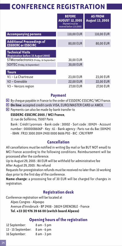
Paymenty By cheque payable in France to the order of ESSDERC-ESSCIRC/ MCI France.y On line: accepted credit cards VISA, EURO/MASTER CARD or AMEX.y Payments can also be made by bank transfer to
ESSDERC-ESSCIRC 2005 / MCI France,11 rue de Solférino, 75007 ParisBank : Crédit Lyonnais - Bank code : 30002 - Sort code : 00424 - Accountnumber : 0000008606P - Key : 61 - Bank agency : Paris rue du Bac (00424)- IBAN : FR33 3000 2004 2400 0000 8606 P93 - BIC : CRLYFRPP
CancellationAll cancellations must be notified in writing (by mail or fax BUT NOT email) toMCI France according to the following conditions. Reimbursement will beprocessed after the conference.Up to August 29, 2005 : 80 EUR will be withheld for administrative feeAfter August 29, 2005 : No refundRequests for preregistration refunds must be received no later than 10 workingdays prior to the first day of the conference.Name change: a processing fee of 30 EUR will be charged for changes inregistration.
Registration deskConference registration will be located at
Alpes Congres - AlpexpoAvenue d'Innsbruck - BP 2408 - 38034 GRENOBLE - FranceTel. +33 (0) 476 39 66 00 (switch board Alpexo)
Opening hours of the registration12 September: 8 am - 5 pm13 - 15 September: 8 am - 6 pm16 September: 8 am - 3 pm
BEFOREAUGUST 12, 2005
(Payment must bereceived before 12.8.2005)
AS FROMAugust 13, 2005
Accompanying persons 110,00 EUR
Additional Proceedings ofESSDERC or ESSCIRC 80,00 EUR
Technical Visits(Registration before 15 August 2005)STMicroelectronics (Friday, 16 September)
SOITEC (Friday, 16 September)
30,00 EUR30,00 EUR
ToursV1 – La ChartreuseV2 – GrenobleV3 – Vercors region
23,00 EUR22,00 EUR27,00 EUR
23,00 EUR22,00 EUR27,00 EUR
110,00 EUR
80,00 EUR
CONFERENCE REGISTRATION

15
Internet servicesComputer terminals with internet access will be available for free on the site of theconference during the opening hours.It will also be possible to use the WIFI network (10 Mbytes/s) of the conferencecenter using your personal laptop. WiFi cards can be purchased at the conferencecenter (2 hours = 9.5 EUR, 24 hours = 29 EUR, 7 days = 99 EUR).
Conference languageThe working language for the conference will be English to be used for allpresentations and printed material.
Insurance disclaimerPlease arrange your own travel and health care insurance. The organizers will notbe held liable for accidents, theft and property damage, nor for delays or anymodification of the programme.
Speakers briefingAuthors should meet their chairperson in the session room 20 minutes prior to thebeginning of their respective sessions.
Guidelines for PresentationsTo ensure a successful presentation, without software compatibility problems,please note the following guidelines:
t Your presentation will take 20 minutes including your introduction by thesession chair and a few minutes for questions from the audience.
t Electronic projection will be used for all presentations (no transparenciesor 35mm slides).
t Your presentation has to be in PDF or PPT format on IBM PC versions ONLY.t Your presentation has to be saved using a file name with the pattern
“S_author_n.pdf”(or .ppt) where S is the session number (see the conferenceprogramme), author is the last name of the first author and n is the versionnumber of your file. Example: 1A1_Einstein_17.ppt.
t Please prepare a SHORT vita (5 lines) so that the chairman can introduceyou.
t The deadline for submission of your presentation is: September, 2nd 2005.Details regarding the exact procedure of submissions will be available onthe ESSDERC & ESSCIRC web site at the beginning of July.
t No correction of your presentation will be possible after September 2.t Computers will be available in the Speaker Preparation Room to review
your file (not to make changes).t Please bring a backup CD or USB key with your presentation just in case.t Despite the fact that the content of electronic presentations is assumed to
be placed in the public domain at the time of the conference, ESSDERC-ESSCIRC'05 will not publish or distribute the presentation files.
Conference proceedingsAll participants will receive a copy of either the ESSDERC or the ESSCIRC Proceedingsand a CDROM with both ESSDERC and ESSCIRC accepted papers.
Best paper awardESSDERC/ESSCIRC offers a “Best Paper” award (for contributed papers only) anda “Young Scientist” award, for the best paper presented by a speaker of less than28 years old. The recipient will be the speaker himself. The selection is based on:(i) evaluation by the audience and (ii) paper ratings.
CONFERENCE INFORMATION

16
SOCIAL PROGRAMMETuesday, 13 September at 7 pm
A welcome reception will be offered by the Mayor of Grenoble, MichelDESTOT, at the “Musée de Grenoble”, 5, place de Lavalette.
City center, tramway stop “Nôtre Dame - Musée”.Shuttle busses from Alpexpo will be arranged at 6:40 pm for the participantsat the Panel Session.
Wednesday, 14 September at 7:30 pmThe Gala dinner will take place at the PRISME Seyssins (89 avenue de Grenoble,38180 Seyssins).
The shuttle buses will leave from Alpexpo at 7 pm.
A cocktail reception before the dinner will be offered by the Mayor ofSeyssins, Didier Migaud.
The morning session on Thursday still starts at 9 am !
Thursday, 15 September at 7:30 pm
Farewell party at the Restaurant du Téléférique, Fort de la Bastille, Grenoble.
To join the restaurant, please take the cable car, the organiser will provide freetickets.Departure : Téléférique Grenoble-Bastille, Quai Stéphane JayThe Farewell evening is sponsored by

17
All tours will be conducted in English.They will depart and return from andto the Conference Center. Theorganisers reserve the right to canceltours with less than 25 participants.Since the excursions have a limitednumber of participants, pleaseregister as soon as possible. Reservations will be made in order ofarrival; on-site availability cannot be guaranteed.
V1 - “La Chartreuse”Tuesday, 13 September 2005 - 1:30pm-6:30pmCost: 23 EUR
This is a land of calm with small and prettyvillages, peaceful forests, mountain passescrossed by winding roads overhanging torrents.Saint Bruno found refuge here more than 900 years ago to meditateand found the famous Grande Chartreuse Monastery. The monasteryis still dedicated to prayer and meditation and part of it can be visited.The tour includes the visit of the distillery in the greatest caves as wellas the tasting of the famous Chartreuse liquor.
ACCOMPANYING PERSONSPROGRAMME
V2 - “Grenoble”Wednesday, 14 September 2005 - 09:00am-01:00pmCost: 22 EUR
This tour is designed to reveal the city's architectural and culturaltreasures such as Saint-André, Notre-Dame and Grenette squares, thepalace of justice, Stendhal's home, the city gardens and old privatemansions from the 15 and 16 centuries so typical with their Renaissancespiral vaulted stairways. Riding the cable car, you will get to the fortifiedsite of the Bastille to admire an astonishing panorama overlookingGrenoble and the surrounding mountains. In clear days Mont Blanccomes nearby!
V3 - “Vercors region”Thursday, 15 September 2005 - 08:30am-01h30pmCost: 27 EUR
The Vercors seems to be an islandsurrounded by land. Water has cut deepgorges, magestic cirques, caves andswallow-holes, among the most famousin the Solar System.Visit of the unforgettable Choranche Caveswith its thousands of spaghetti-likestalactites reflected in the inner mountainlake. The sound and light show is
spectacular. Stop at Pont-en-Royans at the end of the Bournes Gorges:dominated by rocky edges, this very, very old village is suspendedabove the bed of the torrent. Picturesque houses overhang the void.

18
ESSDERC-ESSCIRCJOINT PLENARY TALKS
For details, see Programme ESSCIRC, pages 9-12.
Horst Stormer“Silicon Forever! Really?”
Eli Yablonovitch“Silicon Nano-Photonics: Where the Photons Meet the Electrons”
Michael Shur“Terahertz Electronics: Devices, Circuits, and Applications”
Ralph Cavin“Limits of CMOS Devices and Circuits”
Mike Thompson“Future of CMOS Technology, Manufacturing and Products”
Christian Joachim“Towards a Molecule - Computer? ”
MINATEC - Under construction.
19
ESSDERC-INVITEDPLENARY TALKS
Carlos Mazuré and André-Jacques Auberton-Hervé“Engineering Wafers for the Nanotechnology Era ”
Nanotechnology starts at the substrate level. Substrate engineering is one of themost important innovations of the nanotechnology era driven by the vanishingboundary between substrate design and device architecture. SOI substrates, the firstengineered substrates of its kind, have made possible an efficient optimization ofMOSFET current drive while minimizing the leakage and reducing parasitic elements,thus enhancing the overall IC performance. Strained silicon, hybrid orientation SOI,germanium on insulator have added new handles to traditional scaling to furtherimprove device and IC performance. An overview of the advances in Smart Cutengineered substrates and the impact on device performance will be given.
Biographies
André-Jacques Auberton-Hervé co-founded Soitec with Jean-Michel Lamure in1992, and currently serves as President and CEO, overseeing the strategic,operational and financial activities of the company. Prior to founding Soitec, Dr.Auberton-Hervé managed joint development programs between LETI andThomson-CSF, the ultimate target of which was the technological transfer fromR&D to production. These programs included the transfer of 1.2 µm and 0.8 µmSOI CMOS for space applications. He was also in charge of several projects, whichapplied SOI to 3D integration, VLSI and ULSI. In 1999, he received the EuropeanSEMI Award in recognition of his work on the Smart Cut technology and hiscontribution to the semiconductor industry. Dr. Auberton-Hervé is a member ofthe Electrochemical Society and the IEEE. Dr. Auberton-Hervé has a Ph.D. insemiconductor physics and an M.S. in materials science from Ecole Centrale deLyon (France).Since 2001, Carlos Mazuré, Chief Technology Officer, has managed Soitecs's strategicAdvanced Technology Development organization. He is tasked with identifyingthe best new breed of engineered substrates and its applications to help definethe future business directions for the company. He works closely with Soitec'scustomers to help support and open new applications for Soitec's Smart Cuttechnology. Prior to Soitec, Mazuré served as director of business developmentat Infineon Technologies AG, and was involved with the IBM/Siemens DRAMDevelopment Alliance. His experience also includes work on SOI and BiCMOShigh performance devices and technology development at Motorola Corp. CarlosMazuré holds two doctorates in physics, one from the University of Grenoble,France, and the other from the Technical University of Munich, Germany. CarlosMazuré is the author of more than 150 technical papers and holds more than 70patents worldwide.
Lothar Risch“Pushing CMOS beyond the Roadmap”
The end of CMOS and of Moore's law was already discussed at feature sizes ofabout 1µm in the eighties. Today, the 90 nm generation is in production and inspite of many roadblocks, the latest ITRS expects that CMOS can be scaled at leastdown to the 22 nm node with minimum gate lengths of 9 nm. However, forconventional bulk CMOS serious challenges are evident and new transistors withbetter electrostatic channel control, lower off currents and higher on currents willbe needed. Among them multi-gate devices with very thin silicon channels aremost promising. Several architectures like FinFET, wafer bonded double-gate and

20
ESSDERC-INVITEDSON have been demonstrated with good electrical characteristics at gate lengthsof 25-10 nm. From quantum mechanical simulations with idealized source draindoping profiles it is predicted that silicon MOSFETs will be functional down to 2nm gate length with off currents in the µA/µm range. Multi-gate transistors havealso been implemented in high density Flash memory cells down to 20 nm. Theyachieve large Vt shifts, suitable for multi-level storage. Even single electrons can bedetected on the storage node. To summarize, it seems very realistic that the deviceroadmap will not end at the 22 nm node. Provided that manufacturing and costissues can be fulfilled, CMOS will dominate also in the nanoelectronics era.
BiographyLothar Risch received the diploma degree in physics from the Technical Universityof Berlin in 1974 and the doctor degree from the Technical University of Karlsruhein 1976. He joined Siemens Corporate Research in Munich in 1977. Since then, hehas been engaged in Silicon microelectronics especially in DRAM memory celldevelopment from 4 to 256 Mbit, CMOS logic, and Silicon based nanoelectronics.In 1999 he moved to Infineon Technologies, the former Siemens SemiconductorGroup. Now, he is a senior director of the department Corporate Research NanoDevices with the main activity on 30 to 10nm CMOS and memory cells. He filedmore than 50 patents and he is also a member of several advisory boards andtechnical program committees.
H.-S. Philip Wong“Nanoelectronics: Nanotubes, Nanowires, Molecules and Novel Concepts”As device sizes approach the nanoscale, new opportunities arise from harnessingthe physical and chemical properties at the nanoscale. Chemical synthesis, self-assembly, and templated self-assembly promise the precise fabrication of devicestructures or even the entire functional entity. Quantum phenomena and one-dimensional transport may lead to new functional devices with very differentpower/performance tradeoffs. New materials with novel electronic, optical, andmechanical properties emerge as a result of the ability to manipulate matter ona nanoscale. It is now feasible to contemplate new nanoelectronic systems basedon new devices with completely new system architectures. This paper will givean overview of the materials, technology, and device opportunities in the nanoscaleera. The focus of discussion will be on nanotubes, nanowires, molecular devices,and novel device concepts for nanoelectronics.
BiographyH.-S. Philip Wong joined the IBM T. J. Watson Research Center, Yorktown Heights,New York, in 1988. In September, 2004, he joined Stanford University as Professorof Electrical Engineering. While at IBM, he was Senior Manager of the 60-memberDepartment of Nanoscale Materials, Processes, and Devices. He has theresponsibility of shaping and executing IBM's strategy on nanoscale science andtechnology. Prior to this appointment, he was Senior Manager of the ExploratoryDevices and Integration Technology Department. His 54-member department wasresponsible for defining and executing IBM's exploratory devices and technologyroadmap for silicon technology. His research interests are in nanoscale scienceand technology, semiconductor technology, solid state devices, and electronicimaging. He is interested in exploring new materials, novel fabrication techniques,and novel device concepts for future nanoelectronics systems. Novel devices oftenrequire new concepts in circuit and system designs. His research also includesexplorations into circuits and systems that are device-driven. He is a Fellow of theIEEE. He is a member of the Emerging Research Devices Working Group of theInternational Technology Roadmap for Semiconductors (ITRS).

21
Cambridge University Press is the printing and publishing house of theUniversity of Cambridge. Visit our stand and receive a 20% discount on alldisplayed titles.
Taylor Hobson is an ultra-precision technology company operating at thehighest levels of accuracy within the field of surface and form metrology. Weprovide contact and non-contact measurement solutions to the most demandingapplications on a global basis, with a worldwide infrastructure to support ourclients, wherever they may be.
Silvaco delivers to semiconductor technologists TCAD products to developand optimize their semiconductor processes; to IC designers CAD products todesign and simulate analog circuits and “field solvers” products for accurateparasitics extraction. Interaction between manufacturing and design dependson accurately extracted device models and reliable simulation.
Keithley Instruments provides leading and cost effective solutions for DC toRF test and measurements for high tech industries in semiconductor, wirelesstelecom and nanotechnology domains. For more than 50 years, we havedemonstrated our excellence in electrical characterization of materials,reliability test, failure analysis, data acquisition and process control.
Agilent Advanced Design System (ADS) is the industry leader in high-frequencydesign. It supports system and RF design engineers developing all types of RFdesigns, from simple to the most complex, from RF/microwave modules tointegrated MMICs for communications and aerospace/defense applications.
John Wiley & Sons Ltd are a leading international publisher of print andelectronic products, specialising in scientific and technical books and journals.Visit our stand at ESSDERC-ESSCIRC'05 and view our latest range of circuits &devices publications. All books on display are available at a special conferencediscount. Alternatively view our publications online: www.wiley.com
The exhibition includes major scientific publishers as well as suppliers ofequipments for characterisation, CAD software, test tools and equipment, etc.Opening hours:Tuesday 13 September: 12 am - 5 pmWednesday 14 September: 9 am - 5 pmThursday 15 September: 9 am - 3 pm
EXHIBITORS
22
Welcome to the new Springer!Since the merger of Kluwer Academic Publisher and Springer-Verlag the productrange includes more than 1,200 journals and 3,500 new book titles each year,making Springer the world's second largest supplier of scientific literature.For a comprehensive overview of the Springer publishing program, pleasevisit http://www.springeronline.com
Elsevier is the world's leading publisher of scientific, medical & technicalinformation. Our publications are written and edited by internationallyrenowned scholars with excellent technical and scientific credentials and wideresearch and teaching experience in their fields. Please feel free to visit ourstand and sample some of the journal content for yourself!
CIRCUIT EXHIBITIONAn exhibition of integrated circuits is organised during all the Conference.Three categories of circuits are considered: education, research, industry.All circuits have been fabricated, through different manufacturing services.The circuit exhibition is sponsored by CMP.
Plots of the circuits as well as information on the circuits (function, origin, etc.)are on display on Tuesday, Wednesday and Thursday at the exhibition area.The authors will be present at their posters for discussions and demonstrationsduring the Coffee Breaks on Tuesday. A catalogue is available.
For more information, please contact:Bernard Courtois [email protected] Delori [email protected]
FRINGE MEETINGS
Lunch and Learn Seminar: Pulsed Characterization ofAdvanced CMOS Technologies
Date: Wednesday, 14 September, 12:45-14:15 (and 18:00 – 19:00)Room: BayardOrganised by:KeithleyFor more information please come to our booth at the exhibition area.
Other Fringe Meetings:The topic and location of the fringe meetings will be announced at theconference site.
23
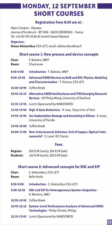
MONDAY, 12 SEPTEMBERSHORT COURSESRegistration from 8:00 am at :
Alpes Congres - AlpexpoAvenue d'Innsbruck - BP 2408 - 38034 GRENOBLE - FranceTel. +33 (0) 476 39 66 00 (switch board Alpexo)
Organiser:Simon Deleonibus CEA-LETI, email: [email protected]
Short course 1: New process and device conceptsChair: F. Balestra, IMEPRoom: Chartreuse
8:50-9:00 Introduction - F. Balestra, IMEP
9:00-10:30 Advanced CMOS Devices on Bulk and SOI: Physics, Modelingand Characterisation - T. Poiroux, CEA LETI
10:30-10:45 Coffee Break
10:45-12:15 Alternative CMOS Architectures and ITRS Emerging ResearchDevices - HS Philip-Wong, University of Stanford
12:15-13:45 Lunch (Sponsored by NANOCMOS)
13:45-14:45 High-K Gate Dielectrics - H. Iwai, Tokyo Inst. of Tech
14:45-15:45 Ion Implantation Damage and Annealing in Silicon - K. Jones,University of Florida
15:45-16:00 Coffee Break
16:00-17:00 New Interconnects Schemes: End of Copper, Optical Inter-connects? - S. Laval, IEF, France
Fees:
Regular: 200 EUR (early), 250 EUR (late)Students: 150 EUR (early), 200 EUR (late)
Short course 2: Advanced concepts for SOC and SIPChair: S. Deleonibus, CEA-LETIRoom: Belle étoile
8:50-9:00 Introduction - S. Deleonibus CEA-LETI
9:00-10:30 SOC and SIP for Heterogeneous System Integration -R. Mertens, IMEC
10:30-10:45 Coffee Break
10:45-12:15 System-Level Performance Analysis of Advanced CMOSTechnologies - Philip Christie, Philips
12:15-13:45 Lunch (Sponsored by NANOCMOS)
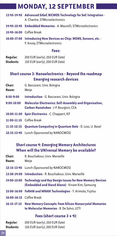
24
MONDAY, 12 SEPTEMBER13:45-14:45 Advanced SiGeC BICMOS Technology for SoC Integration -
A. Chantre, STMicroelectronics
14:45-15:45 Embedded Memories - A. Maurelli, STMicroelectronics
15:45-16:00 Coffee Break
16:00-17:00 Introducing New Devices on Chip: MEMS, Sensors, etc. -P. Ancey, STMicroelectronics
Fees:Regular: 200 EUR (early), 250 EUR (late)Students: 150 EUR (early), 200 EUR (late)
Short course 3: Nanoelectronics - Beyond the roadmapEmerging research devices
Chair: G. Baccarani, Univ. BolognaRoom: Meije
8:50-9:00 Introduction - G. Baccarani, Univ. Bologna
9:00-10:00 Molecular Electronics: Self-Assembly and Organisation,Carbon Nanotubes - J-P. Bourgoin, CEA
10:00-11:00 Spin Electronics - C. Chappert, IEF
11:00-11:15 Coffee Break
11:15-12:15 Quantum Computing in Quantum Dots - D. Loss, U. Basel
12:15-13:45 Lunch (Sponsored by NANOCMOS)
Short course 4: Emerging Memory ArchitecturesWhen will the UNIversal Memory be available?
Chair: R. Bouchakour, Univ. MarseilleRoom: Meije
12:15-13:45 Lunch (Sponsored by NANOCMOS)
13:50-14:00 Introduction - R. Bouchakour, Univ. Marseille
14:00-15:00 Technology and Key Design Issues for New Memory Devices(Embedded and Stand Alone) - Kinam Kim, Samsung
15:00-16:00 FeRAM and MRAM Technologies - Y. Arimoto, Fujitsu
16:00-16:15 Coffee Break
16:15-17:15 New Memory Concepts: from Silicon Nanocrystal Memoriesto Molecular Memories - B. De Salvo, LETI
Fees (short course 3 + 4):Regular: 200 EUR (early), 250 EUR (late)Students: 150 EUR (early), 200 EUR (late)
25
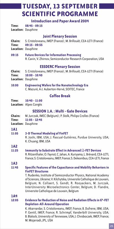
TUESDAY, 13 SEPTEMBERSCIENTIFIC PROGRAMME
Introduction and Paper Award 2004Time: 08:45 - 09:15Location: Dauphine
Joint Plenary SessionChairs: S. Cristoloveanu, IMEP (France) ; M. Brillouët, CEA-LETI (France)Time: 09:15 - 09:55Location: Dauphine
09:15 Future Devices for Information ProcessingR. Cavin, V. Zhirnov, Semiconductor Research Corporation, USA
ESSDERC Plenary SessionChairs: S. Cristoloveanu, IMEP (France) ; M. Brillouët, CEA-LETI (France)Time: 10:00 - 10:40Location: Dauphine
10:00 Engineering Wafers for the Nanotechnology EraC. Mazuré, A-J. Auberton-Hervé, SOITEC, France
Coffee BreakTime: 10:40 - 11:00Location: Alpes Congès
SESSION 1.A. : Multi - Gate DevicesChairs: M. Jurczak, IMEC (Belgium) ; P. Stolk, Philips Crolles (France)Time: 11:05 - 12:45Location: Dauphine
1A111:05 3-D Thermal Modeling of FinFET
R. Joshi, IBM, USA; J. Pascual-Gutiérrez, Purdue University, USA;K. Chuang, IBM, USA
1A211:25 Immunity to Substrate Effect in Advanced Ω-FET Devices
R. Ritzenthaler, O. Faynot, C. Jahan, A. Kuriyama, L. Brévard, CEA-LETI,France; S. Cristoloveanu, IMEP, France; S. Deleonibus, CEA-LETI, France
1A311:45 Specific Features of the Capacitance and Mobility Behaviors in
FinFET StructuresT. Rudenko, Institute of Semiconductor Physics, National Academyof Sciences, Ukraine; V. Kilchytska, Universite Catholique de Louvain,Belgium; N. Collaert, S. Gendt, R. Rooyackers, M. Jurczak,InterUniversity Microelectronics Center, Belgium; D. Flandre,Universite Catholique de Louvain, Belgium
1A412:05 Evidence for Reduction of Noise and Radiation Effects in G4-FET
Depletion-All-Around OperationK. Akarvardar, S. Cristoloveanu, IMEP, France; B. Dufrene, IBM, USA;P. Gentil, IMEP, France; R. Schrimpf, Vanderbilt University, USA;B. Blalock, University of Tennessee, USA; J. Chroboczek, IMEP, France;M. Mojarradi, JPL, USA

26
TUESDAY, 13 SEPTEMBER1A512:25 Tunneling and Intersubband Coupling in Ultra-Thin Body
Double-Gate MOSFETsV. Sverdlov, Institute for Microelectronics, TU Vienna, Austria;A. Gehring, AMD Saxony LLC & Co. KG, Germany; H. Kosina,S. Selberherr, Institute for Microelectronics, TU Vienna, Austria
SESSION 1.B. : Gate StackChairs: J. Hooker, Philips Leuven (Belgium) ; R. Beck, Warsaw University of
Technology (Poland)Time: 11:05 - 12:45Location: Oisans
1B111:05 Germanium/HfO2/TiN Gate Stacks for Advanced Nodes:
Influence of Surface Preparation on MOS CapacitorCharacteristicsC. Le Royer, X. Garros, C. Tabone, L. Clavelier, CEA-LETI, France;Y. Morand, STMicroelectronics, France; J. Hartmann, CEA-LETI, France;Y. Campidelli, O. Kermarrec, ST Microelectronics, France; V. Loup,E. Martinez, O. Renault, B. Guigues, CEA-LETI, France; V. Cosnier, STMicroelectronics, France; S. Deleonibus, CEA-LETI, France
1B211:25 The Effect of Metal Thickness, Overlayer and High-k Surface
Treatment on the Effective Work Function of Metal ElectrodeK. Choi, H. Wen, SEMATECH, USA; H. Alshareef, TI, SEMATECH, USA;R. Harris, P. Lysaght, H. Luan, P. Majhi, B. Lee, SEMATECH, USA
1B311:45 Mixed-Signal and Noise Properties of nMOSFETs with
HfSiON/TaN Gate StacksC. Rittersma, Philips Research Leuven, Belgium; E. Simoen,P. Srinivasan, IMEC, Belgium; M. Vertregt, Philips Research, TheNetherlands; C. Claeys, IMEC, Belgium
1B412:05 Work Function Control of Metal Gates by Interdiffused Ni-Ta with
High Thermal StabilityT. Matsukawa, Y. Liu, M. Masahara, K. Endo, K. Ishii, H. Yamauchi,E. Sugimata, H. Takashima, E. Suzuki, S. Kanemaru, NanoeletronicsReseach Inst., AIST, Japan
1B512:25 PLAsma Doping for S/D Extensions: Device Integration, Gate
Oxide Reliability and Dynamic BehaviorB. Dumont, STMicroelectronics, France; A. Pouydebasque, PhilipsSemiconductors, France; F. Lallement, D. Lenoble, G. Ribes, J. Roux,STMicroelectronics, France; S. Vanbergue, Philips Semiconductors,France; T. Skotnicki, STMicroelectronics, France
SESSION 1.C. : RF DevicesChairs: P. Ashburn, University of Southampton (United Kingdom) ;
S. Decoutere, IMEC (Belgium)Time: 11:05 - 12:45Location: Sept Laux
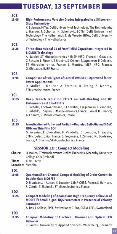
27
TUESDAY, 13 SEPTEMBER1C111:05 High-Performance Varactor Diodes Integrated in a Silicon-on-
Glass TechnologyK. Buisman, HiTec, Delft University of Technology, The Netherlands;L. Nanver, T. Scholtes, H. Schellevis, ECTM, Delft University ofTechnology, The Netherlands; L. de Vreede, HiTec, Delft Universityof Technology, The Netherlands
1C211:25 Three-dimensional 35 nF/mm2 MIM Capacitors Integrated in
BiCMOS TechnologyA. Bajolet, ST Microelectronics / IMEP-INPG, France; J. Giraudin,C. Rossato, L. Pinzelli, S. Bruyère, S. Crémer, T. Jagueneau, P. Delpech,ST Microelectronics, France; L. Montès, IMEP-INPG, France;G. Ghibaudo, IMEP, France
1C311:45 Comparison of two Types of Lateral DMOSFET Optimized for RF
Power ApplicationsD. Muller, J. Mourier, A. Perrotin, B. Szelag, A. Monroy,STMicroelectronics, France
1C412:05 Deep Trench Isolation Effect on Self-Heating and RF
Performances of SiGeC HBTsB. Barbalat, T. Schwartzmann, P. Chevalier, T. Jagueneau, B. Vandelle,L. Rubaldo, F. Saguin, STMicroelectronics, France; F. Aniel, IEF, France;A. Chantre, STMicroelectronics, France
1C512:25 Investigation of Fully- and Partially-Depleted Self-Aligned SiGeC
HBTs on Thin Film SOIG. Avenier, P. Chevalier, B. Vandelle, D. Lenoble, F. Saguin,STMicroelectronics, France; S. Frégonese, T. Zimmer, IXL Bordeaux,France; A. Chantre, STMicroelectronics, France
SESSION 1.D. : Compact ModelingChairs: H. Jaouen, STMicroelectronics Crolles (France) ; K. McCarthy, University
College Cork (Ireland)Time: 11:05 - 12:45Location: Stendhal
1D111:05 Quantum Short-Channel Compact Modeling of Drain-Current in
Double-Gate MOSFETD. Munteanu, J. Autran, X. Loussier, L2MP-CNRS, France; S. Harrison,R. Cerutti, T. Skotnicki, ST Microelectronics, France
1D211:25 Compact Modeling of Anomalous High Frequency Behavior of
MOSFET's Small-Signal NQS Parameters in Presence of VelocitySaturationA. Roy, J. Sallese, EPFL, Switzerland; C. Enz, CSEM, EPFL, Switzerland
1D311:45 Compact Modeling of Electrical, Thermal and Optical LED
BehaviorP. Baureis, University of Applied Sciences, Wuerzburg, Germany
28
TUESDAY, 13 SEPTEMBER1D412:05 A Closed-Form Charge-Based Expression for Drain Current in
Symmetric and Asymmetric Double Gate MOSFETA. Roy, EPFL, Switzerland; J. Sallese, EFPL, Switzerland; C. Enz,CSEM,EPFL, Switzerland
1D512:25 Base-Collector Junction Charge Investigation of Si/SiGe HBT on
Thin Film SOIS. Frégonese, IXL, France; G. Avenier, STMicroelectronics, France;C. Maneux, IXL, France; A. Chantre, STMicroelectronics, France;T. Zimmer, IXL, France
LunchTime: 12:45 - 14:10Location: Les Ecrins
Joint Plenary SessionChairs: M. Steyaert, Katholieke Universiteit Leuven (Belgium) ; W. Redman-
White, Philips Semiconductors (UK)Time: 14:15 - 14:55Location: Dauphine
14:15 Silicon Nano-Photonics: Where the Photons Meet the ElectronsE. Yablonovitch, Electrical Engineering Department, University ofCalifornia, USA
SESSION 2.A. : Nano-Scaled DevicesChairs: G. Iannacconne, University of Pisa (Italy) ; L. Risch, Infineon (Germany)Time: 15:00 - 16:40Location: Chartreuse
2A115:00 Nanotechnology: Potential Challenger to Silicon CMOS? (Invited)
B. Yu, NASA Ames Reserach Center, USA; M. Meyyappan, NASA AmesResearch Center, USA
2A215:20 Quantum-Mechanical Analysis of the Electrostatics in Silicon-
Nanowire and Carbon-Nanotube FETsE. Gnani, A. Marchi, S. Reggiani, M. Rudan, G. Baccarani, ARCES -University of Bologna, Italy
2A315:40 Trade-off between Electron Velocity and Density of States in
Ballistic Nano-MOSFETsM. De Michielis, D. Esseni, F. Driussi, DIEGM, Univ. of Udine, Italy
2A416:00 Monte Carlo Simulations of Sub-100 nm InGaAs MOSFETs for
Digital ApplicationsK. Kalna, University of Glasgow, UK; L. Yang, Cadence Ltd., China; A.Asenov, University of Glasgow, UK

29
TUESDAY, 13 SEPTEMBER2A516:20 The 65nm Tunneling Field Effect Transistor (TFET) 0.68 µm2 6T
Memory Cell and Multi-Vth DeviceT. Nirschl, Infineon Technologies, Germany; S. Henzler, J. Fischer,A. Bargagli-Stoffi, M. Fulde, M. Sterkel, Technical University Munich,Germany; U. Schaper, G. Georgakos, Infineon Technologies, Germany;D. Schmitt-Landsiedel, Technical University Munich, Germany
SESSION 2.B. : Dynamic Random Access MemoriesChairs: P. Erratico, STMicroelectronics Agrate (Italy) ; S. Okhonin, Innovative
Silicon (Switzerland)Time: 15:00 - 16:40Location: Belle étoile
2B115:00 High-Density Low-Power-Operating DRAM Device Adopting 6F2
Cell Scheme with Novel S-RCAT Structure on 80nm Feature SizeH. Oh, J. Kim, J. Kim, S. Park, D. Kim, S. Kim, D. Woo, Y. Lee, G. Ha, J.Park, N. Kang, H. Kim, Y. Hwang, B. Kim, D. Kim, Y. Choi, J. Choi, B. Lee,S. Kim, M. Cho, Y. Kim, J. Choi, D. Shin, M. Shim, W. Choi, G. Lee, Y.Park, W. Lee, B. Ryu, Samsung Electronics Co, Korea
2B215:20 Advanced Memory Concepts for DRAM and Nonvolatile
Memories (Invited)F. Horiguchi, Toyo University, Japan
2B315:40 Data Retention Analysis on Individual Cells of 256Mb DRAM in
110nm TechnologyA. Weber, Infineon Technologies / TU Harburg, Germany; A. Birner,Infineon Technologies, Germany; W. Krautschneider, TU Harburg,Germany
2B416:00 Enhancement of Data Retention Time in DRAM using Step gaTed
AsymmetRic (STAR) Cell TransistorsM. Jang, M. Seo, Y. Kim, S. Cha, S. Park, S. Pyi, J. Jeong, S. Hong, S. Park,Hynix Semiconductor Inc., Korea
2B516:20 Analysis of the NAND-type DRAM-on-SGT for High-Density and
Low-Voltage MemoryH. Nakamura, I. Pesic, H. Sakuraba, F. Masuoka, Research Institute ofElectrical Communication, Tohoku University, Japan
SESSION 2.C. : High- and Medium-K CharacterisationChairs: S. Bengtsson, Chalmers University (Sweden) ; G. Groeseneken, IMEC
(Belgium)Time: 15:00 - 16:20Location: Meije

30
TUESDAY, 13 SEPTEMBER2C115:00 Polarity Dependence of Bias Temperature Instabilities in
Hf(x)Si (1-x) ON/TaN Gate StacksM. Aoulaiche, M. Houssa, R. Degraeve, G. Groeseneken, S. De Gendt,M. Heyns, IMEC, Belgium
2C215:20 The Role of Nitrogen Incorporation in Hf-based High-k Dielectrics:
Reduction in Electron Charge TrapsN. Umezawa, National Institute for Materials Science, Japan;K. Shiraishi, Univ. of Tsukuba, Japan; K. Torii, Semiconductor LeadingEdge Technology Inc., Japan; T. Chikyow, National Institute forMaterials Science, Japan; H. Watanabe, Osaka Univ., Japan; K. Yamabe,Univ. of Tsukuba, Japan; T. Ohno, Institute for Materials Science,Japan; K. Yamada, Waseda Univ., Japan; Y. Nara, SemiconductorLeading Edge Technology Inc., Japan; M. Boero, Univ. of Tsukuba,Japan
2C315:40 Effects of Plasma Nitridation on the Electrical Properties of
Nitrided Oxide Gate Dielectric for DRAM ApplicationJ. Heo, D. Kim, B. Koo, J. Kim, C. Kim, Y. Noh, S. Baek, Y. Shin, U. Chung,Samsung Electronics Co., Korea
2C416:00 A New Method Based on Charge Pumping Technique to Extract
the Lateral Profiles of Localized Charge Trapping in NitrideH. Pang, L. Pan, L. Sun, Y. Zeng, Z. Zhang, J. Zhu, Institute ofMicroelectronics, Tsinghua University, China
SESSION 2.D. : NanowiresChairs: M. Sanquer, CEA (France) ; O. Engström, Chalmers University (Sweden)Time: 15:00 - 16:40Location: Sept Laux
2D115:00 Analytical Model for Nanowire and Nanotube Transistors
Covering both Dissipative and Ballistic TransportG. Mugnaini, G. Iannaccone, University of Pisa, Italy
2D215:20 High Performance ZnO Nanowire Field Effect Transistor
S. Cha, J. Jang, Y. Choi, G. Ho, D. Kang, D. Hasko, M. Welland, G.Amaratunga, University of Cambridge, UK
2D315:40 Impact of Point Defect Location in Nanowire Silicon MOSFETs
M. Bescond, University of Glasgow, UK; N. Cavassilas, K. Nehari, J.Autran, M. Lannoo, L2MP UMR CNRS 6137, France; A. Asenov,University of Glasgow, UK
2D416:00 Detection of Individual Traps in Silicon Nanowire Transistors
M. Hofheinz, X. Jehl, M. Sanquer, G. Molas, M. Vinet, S. Deleonibus,CEA Grenoble, France
31
TUESDAY, 13 SEPTEMBER
Welcome Reception at the “Musée de Grenoble”
Time: 19:00
2D516:20 Influence of Band-Structure on Electron Ballistic Transport in
Silicon Nanowire MOSFET's: an Atomistic StudyK. Nehari, N. Cavassilas, J. Autran, L2MP-CNRS, France; M. Bescond,University of Glasgow, UK; D. Munteanu, M. Lannoo, L2MP-CNRS,France
Coffee BreakTime: 16:40 - 17:00Location: Salle de Réception
RUMP SESSION: Where will the revolutionary solutionscome from: technology or design?
Time: 17:00 - 18:30Location: Dauphine
Moderators : T. Skotnicki (STMicroelectronics, France) , A. Kaiser (IEMN, France)
ESSDERC Panelists : Hiroshi IWAI (Tokyo Institute of Technology, Japan) Rainer WASER (RWTH-Aachen, Germany) Kazunari ISHIMARU (SoC R&D Center, TOSHIBA Corp., Japan) Peter ZEITZOFF (SEMATECH, USA)
ESSCIRC Panelists: Clive BITTLESTONE (Texas Instruments, USA) Georges GIELEN (K.U. Leuven, Belgium) Sreedhar NATARAJAN (Emerging Memory Technologies, Canada) Yannis TSIVIDIS (Columbia University, USA)
This rump session brings together eight international experts intechnology/devices and advanced design. Each panelist represents adifferent area of the technology or design: from CMOS manufacturing andadvanced Si devices to nanoelectronics beyond CMOS, from analog & RFto memory and CAD. Short presentations are given to stimulate questionsand comments from the audience. What are the bottlenecks? What are theperspectives for breakthrough solutions? Will they come from thetechnology/device side, from the design side, or from both?

32
WEDNESDAY, 14 SEPTEMBERSCIENTIFIC PROGRAMME
Joint Plenary SessionChairs: C. Enz, CSEM (Switzerland) ; E. Perea, STMicroelectronics (France)Time: 09:00 - 09:40Location: Dauphine
09:00 Terahertz Technology: Devices and ApplicationsM. Shur, ECSE Department and Broadband Center, RensselaerPolytechnic Institute, USA
SESSION 3.A. : RF and Power SOIChairs: M. Östling, KTH (Sweden) ; J. Burghartz, DIMES (The Netherlands)Time: 09:45 - 11:05Location: Chartreuse
3A109:45 Efficient Crosstalk Reduction Using Very Low Resistivity SOI
SubstrateJ. Ankarcrona, L. Vestling, K. Eklund, J. Olsson, Uppsala University,Sweden
3A210:05 SOA Improvement of P-Channel High-Voltage SOI Devices
S. Schwantes, M. Graf, V. Dudek, Atmel Germany, Germany
3A310:25 SOI CMOS Technology for RF/Analog Applications -
Active/Passive Devices and New Crosstalk Isolation Technology(Invited)R. Huang, G. Zhang, H. Liao, L. Yang, T. Yan, Y. Zhou, X. Zhang, Y. Wang,Institute of Microelectronics, Peking University, China
3A410:45 Temperature Dependence of Avalanche Multiplication in
Submicron Silicon DevicesD. Massey, J. David, G. Rees, Department of Electronic and ElectricalEngineering, University of Sheffield, UK
SESSION 3.B. : Nanoscale and Organic DevicesChairs: P. Heremans, IMEC (Belgium) ; E. Cantatore, Philips Leuven (Belgium)Time: 09:45 - 11:05Location: Sept Laux
3B109:45 Digital Logic Using Magnetic Nanostructures (Invited)
R. Cowburn, Imperial College London, Blackett Physics Laboratory,UK
3B210:05 Modelling of Polymer Schottky Diodes for Real Device
ApplicationsM. Raja, N. Sedghi, B. Eccleston, S. Badriya, S. Higgins, University ofLiverpool, UK; G. Lloyd, Merck Chemicals Ltd, UK

33
WEDNESDAY, 14 SEPTEMBER3B310:25 High-Speed InP-based Resonant Tunnelling Diode on Silicon
SubstrateW. Prost, V. Khorenko, University Duisburg-Essen, Germany; A. Mofor,A. Bakin, Technical University Braunschweig, Germany; E. Khorenko,S. Ehrich, University Duisburg-Essen, Germany; H. Wehmann, A.Schlachetzki, Technical University Braunschweig, Germany; F. Tegude,University Duisburg-Essen, Germany
3B410:45 Organic CuTCNQ Non-Volatile Memories for Integration in the
CMOS Backend-of-Line: Preparation from Gas/Solid Reactionand Downscaling to an Area of 0.25 µm2
R. Müller, S. De Jonge, K. Myny, D. Wouters, J. Genoe, P. Heremans,IMEC, Belgium
SESSION 3.C. : Back-End Characterisation and ReliabilityChairs: G. Ghibaudo, IMEP (France) ; J-L. Autran, Université d'Aix-Marseille
(France)Time: 09:45 - 11:05Location: Meije
3C109:45 Characterization and Modeling of Al2O3 MIM Capacitors:
Temperature and Electrical Field EffectsS. Bécu, S. Crémer, O. Noblanc, ST Microelectronics, France; J. Autran,L2MP, UMR CNRS 6137, France; P. Delpech, ST Microelectronics, France
3C210:05 Precise Analogue Characterization of MIM Capacitors Using an
Improved Charge-Based Capacitance Measurement (CBCM)TechniqueZ. Ning, H. Delecourt, L. De Schepper, R. Gillon, M. Tack, AMISemiconductor, Belgium
3C310:25 Distinction of Intrinsic and Extrinsic Breakdown Failure Modes
of Cu/Low-k InterconnectsN. Hwang, Institute of Microelectronics, Singapore; T. Tan, C. Gan,Nanyang Technological University, Singapore
3C410:45 Magnetic Sensing as Signal Integrity Monitoring in Integrated
CircuitsE. Gutierrez INAOE / INTEL, Mexico; E. Torres, R. Torres, INAOE, Mexico
SESSION 3.D. : Transport in Novel MaterialsChairs: E. Sangiorgi, University of Bologna (Italy) ; G. Le Carval, CEA-LETI
(France)Time: 09:45 - 11:05Location: Belle étoile
34
3D109:45 Strained Si/SiGe MOSFET Capacitance Modeling Based on Band
Structure AnalysisF. Gilibert, STMicroelectronics/L2MP, France; D. Rideau,STMicroelectronics, France; F. Payet, STMicroelectronics/L2MP, France;F. Boeuf, E. Batail, M. Minondo, STMicroelectronics, France; R.Bouchakour, L2MP, France; T. Skotnicki, H. Jaouen, STMicroelectronics,France
3D210:05 Physics and Modeling of Ge-On-Insulator MOSFETs (Invited)
A. Chin, H. Kao, Y. Tseng, D. Yu, C. Chen, National Chiao-Tung Univ.,Taiwan; S. McAlister, National Research Council of Canada, Canada;C. Chi, National Tsing Hua Univ., Taiwan
3D310:25 Variations of Hole Mass in p-MOSFETs under Process-Induced
Mechanical StressT. Guillaume, M. Mouis, IMEP, France
3D410:45 A Semi-Empirical Surface Scattering Model for Quantum
Corrected Monte Carlo Simulation of Strained Si-nMOSFETsA. Pham, C. Nguyen, C. Jungemann, B. Meinerzhagen, NST, TU-Braunschweig, Germany
Coffee Break (Sponsored by Mentor Graphics)Time: 11:05 - 11:25Location: Salle de Réception
SESSION 4.A. : Strain EngineeringChairs: K. Ishimaru, Toshiba (Japan) ; S. Koester, IBM (USA)Time: 11:25 - 12:45Location: Chartreuse
4A111:25 In-Depth Study of Strained SGOI nMOSFETs down to 30nm Gate
LengthF. Andrieu, T. Ernst, O. Faynot, O. Rozeau, CEA-LETI, France;Y. Bogumilowicz, STMicroelectronics, France; J. Hartmann, L. Brévard,A. Toffoli, D. Lafond, H. Dansas, CEA-LETI, France; B. Ghyselen, SOITEC,France; F. Fournel, CEA-LETI, France; G. Ghibaudo, IMEP, France; S.Deleonibus, CEA-LETI, France
4A211:45 On the Scalability of Source/Drain Current Enhancement in Thin
Film sSOIE. Augendre, G. Eneman, A. De Keersgieter, V. Simons, I. De Wolf,J. Ramos, IMEC, Belgium; B. Pawlak, Philips Research Leuven, Belgium;L. Fei, MEMC, USA; M. Goodwin, Texas Instruments, USA; S. Brus,S. Severi, F. Leys, E. Sleeckx, S. Locorotondo, M. Ercken, J. de Marneffe,IMEC, Belgium; M. Seacrist, B. Kellerman, MEMC, USA; M. Goodwin,Texas Instruments, USA; K. De Meyer, M. Jurczak, S. Biesemans, IMEC,Belgium
WEDNESDAY, 14 SEPTEMBER
35
WEDNESDAY, 14 SEPTEMBER4A312:05 A Highly Robust SiGe Source Drain Technology Realized by
Disposable Sidewall Spacer (DSW) for 65nm Node and BeyondY. Kim, T. Mori, Y. Hayami, T. Yamamoto, H. Morioka, H. Kokura,K. Kawamura, Y. Shimamune, A. Katakami, A. Hatada, M. Shima,N. Tamura, H. Ohta, T. Sakuma, M. Kojima, M. Nakaishi, T. Sugii,M. Miyajima, Fujitsu Limited, Japan
4A412:25 High Performance Device Utilizing Ultra-Thick-Strained-Si (UTSS)
Grown on Relaxed SiGeS. Lee, Y. Kim, Y. Lee, J. Lee, I. Jung, D. Lee, Y. Shin, U. Chung, J. Moon,Samsung Electronics, Korea
SESSION 4.B. : Non-Volatile Memories IChairs: S. Hall, University of Liverpool (UK) ; A. Schenk, Integrated Systems
Laboratory (Switzerland)Time: 11:25 - 12:45Location: Belle étoile
4B111:25 µ Trench Phase-Change Memory Cell Engineering and
OptimizationA. Pirovano, F. Pellizzer, A. Redaelli, I. Tortorelli, E. Varesi, F. Ottogalli,T. Marangon, A. Lacaita, R. Bez, STMicroelectronics, Italy; M. Tosi,P. Besana, R. Cecchini, R. Piva, M. Magistretti, M. Scaravaggi, G. Mazzone,P. Petruzza, F. Bedeschi, A. Modelli, ST Microelectronics, Italy; D. Ielmini,DEI, Politecnico di Milano, Italy
4B211:45 Gate Current in Stacked Dielectrics for Advanced FLASH EEPROM
cellsF. Driussi, S. Marcuzzi, P. Palestri, L. Selmi, University of Udine, Italy
4B312:05 Anomalous Charge Loss of Reference Cell in MLC Flash Memory
Due to Process-Induced Mobile IonS. Sim, W. Kwon, H. Lee, J. Han, S. Jeon, B. Lee, J. Kim, J. Han, B. Yoon,W. Lee, C. Park, K. Kim, Samsung Electronics, Korea
4B412:25 High Work-Function Metal Gate and High-K Dielectrics for Charge
Trap Flash Memory Device ApplicationsS. Jeon, J. Han, J. Lee, C. Choi, Samsung Advanced Institute ofTechnology, Korea; S. Choi, H. Hwang, Gwangju Institute of Scienceand Technology, Korea; C. Kim, Samsung Advanced Institute ofTechnology, Korea
SESSION 4.C. : Noise and Fluctuations in Nanometer MOSFETsChairs: A. De Keersgieter, IMEC (Belgium) ; M. Rudan, University of Bologna
(Italy)Time: 11:25 - 12:45Location: Meije

36
4C111:25 Do Hot Electrons Produce Excess Noise?
C. Jungemann, B. Meinerzhagen, NST, TU Braunschweig, Germany
4C211:45 A Physics-Based Low Frequency Noise Model for MOSFETs under
Periodic Large Signal ExcitationR. Brederlow, Infineon, Germany; J. Koh, Samsung, Korea; R. Thewes,Infineon, Germany
4C312:05 Simulation of Combined Sources of Intrinsic Parameter
Fluctuations in a 'Real' 35 nm MOSFETG. Roy, F. Adamu-Lema, A. Brown, S. Roy, A. Asenov, GlasgowUniversity, UK
4C412:25 Convergence of the Legendre Polynomial Expansion of the
Boltzmann Equation for Nanoscale DevicesC. Jungemann, NST, TU Braunschweig, Germany; M. Bollhoefer, TUBerlin, Germany; B. Meinerzhagen, NST, TU Braunschweig, Germany
LunchTime: 12:45 - 14:10Location: Les Ecrins
Joint Plenary SessionChairs: H. Iwai, Tokyo Institute of Technology (Japan) ; F. Balestra, IMEP
(France)Time: 14:15 - 14:55Location: Dauphine
14:15 Future of CMOS Technology, Manufacturing and ProductsM. Thompson, STMicroelectronics, France
ESSDERC Plenary SessionChairs: H. Iwai, Tokyo Institute of Technology (Japan) ; F. Balestra, IMEP
(France)Time: 15:00 - 15:40Location: Dauphine
15:00 Nanoelectronics: Nanotubes, Nanowires, Molecules, and NovelConceptsH.-S. P. Wong, Center for Integrated Systems and Department ofElectrical Engineering, Stanford University, USA
Coffee Break (Sponsored by Mentor Graphics)Time: 15:40 - 16:00Location: Alpes Congrès
SESSION 5.A. : Biological and Optical DevicesChairs: R. Thewes, Infineon (Germany) ; R. Mertens, IMEC (Belgium)Time: 16:00 - 17:40Location: Stendhal
WEDNESDAY, 14 SEPTEMBER
37
WEDNESDAY, 14 SEPTEMBER5A116:00 BioMEMS in Medicine: Diagnostic and Therapeutic Systems
(Invited)K. Cheung, P. Renaud, EPFL, Switzerland
5A216:20 Genetically-Engineered Whole-Cell Bioreporters on Integrated
Circuits for Very Low-Level Chemical SensingS. Islam, B. Weathers, M. Zhang, B. Blalock, S. Ripp, G. Sayler, S. Terry,S. Caylor, University of Tennessee, USA
5A316:40 Large-Area Avalanche Diodes for Picosecond Time-Correlated
Photon CountingA. Gulinatti, I. Rech, Politecnico di Milano, Dipartimento di Elettronicae Informazione, Italy; P. Maccagnani, IMM-CNR, Italy; M. Ghioni,S. Cova, Politecnico di Milano, Dipartimento di Elettronica eInformazione, Italy
5A417:00 The Effect of Dislocation Loops on the Light Emission of Silicon
LEDsT. Hoang, P. Leminh, J. Holleman, J. Schmitz, University of Twente, TheNetherlands
5A517:20 Detection of THz Electromagnetic Radiation with Si/SiGe HFET
S. Richard, N. Zerounian, P. Boucaud, IEF, Université Paris-Sud 11,France; J. Ortega, LURE, Université Paris-Sud 11, France; T. Hackbarth,H. Herzog, DaimlerChrysler Research Center, Germany; F. Aniel, IEF,Université Paris-Sud 11, France
SESSION 5.B. : High-K DielectricsChairs: A. Bauer, FhG, Erlangen (Germany) ; E. Augendre, IMEC (Belgium)Time: 16:00 - 18:00Location: Oisans
5B116:00 Mobility Enhancement of High-k Gate Stacks through Reduced
Transient ChargingP. Kirsch, J. Sim, S. Song, S. Krishnan, J. Peterson, H. Li, M. Quevedo-Lopez, C. Young, R. Choi, N. Moumen, P. Majhi, SEMATECH, USA;Q. Wang, J. Ekerdt, The University of Texas, USA; G. Bersuker, B. Lee,SEMATECH, USA
5B216:20 Investigation on the Compositionally Graded HfxAlyOz Films for
TiN Based DRAM CapacitorD. Kil, K. Hong, S. Yeom, H. Song, K. Park, J. Roh, N. Kwak, H. Sohn, J.Kim, S. Park, Hynix, Korea
5B316:40 Scalability and Reliability of TaN/HfN/HfO2 Gate Stacks
Fabricated by a High Temperature ProcessJ. Kang, Peking University, China; H. Yu, IMEC, Belgium; C. Ren, NationalUniversity of Singapore, Singapore; H. Yang, N. Sa, X. Liu, R. Han,Peking University, China; M. Li, D. Chan, National University ofSingapore, Singapore; D. Kwong, The University of Texas, USA
38
5B417:00 Accurate Investigation of the High-k Soft Phonon Scattering
Mechanism in Metal Gate MOSFETsO. Weber, M. Cassé, L. Thévenod, CEA-LETI, France; F. Ducroquet,CEA-LETI/CNRS, France; T. Ernst, CEA-LETI, France; B. Guillaumot,STMicroelectronics, France; S. Deleonibus, CEA-LETI, France
5B517:20 Suppression of Chemical Phase Separation in High-k
Zirconium an Hafnium Nitro-Silicate and Alumino-SilicateAlloys for CMOS ApplicationsG. Lucovsky, NC State University, USA; J. Phillips, Rutgers University,USA; J. Whitten, NC State University, USA
5B617:40 The Effect of Y2O3 Buffer Layer for La2O3 Gate Dielectric Film
K. Nakagawa, K. Miyauchi, K. Kakushima, T. Hattori, FrontierCollaborative Research Center, Tokyo Institute of Technology, Japan;K. Tsutsui, Interdisciplinary Graduate School of Sci, and Eng., TokyoInstitute of Technology, Japan; H. Iwai, Frontier Collaborative ResearchCenter, Tokyo Institute of Technology, Japan
SESSION 5.C. : Oxide Reliability and ESDChairs: R. Woltjer, Philips Leuven (The Netherlands) ; J. Schmitz, University
of Twente (The Netherlands)Time: 16:00 - 18:00Location: Dauphine
5C116:00 MOS Gate Current Characteristics and their Implications for
Lifetime Area ScalingS. Kleff, R. Bottini, G. Ghidini, STMicroelectronics, Italy
5C216:20 Effect of Hot Carrier Stress on the Performance, Trap Densities
and Transient Behavior of SLS ELA TFTsD. Kouvatsos, Institute of Microelectronics, NCSR Demokritos, Greece;G. Papaioannou, M. Exarchos, L. Michalas, Solid State Section, PhysicsDepartment, University of Athens, Greece; A. Voutsas, LCD ProcessTechnology Laboratory, Sharp Labs, USA
5C316:40 New Perspectives on NBTI in Advanced Technologies: Modelling
and CharacterizationM. Denais, STMicroelectronics, France; V. Huard, PhilipsSemiconductors , France; C . Part hasarat hy, G. Ribes,STMicroelectronics, France; F. Perrier, Philips semiconductors, France;D. Roy, STMicroelectronics, France; A. Bravaix, L2MP-ISEM, France
5C417:00 Modeling MOSFET and Circuit Degradation through SPICE
A. Cester, S. Gerardin, A. Paccagnella, University of Padova, Italy; G.Ghidini, ST Microelectronics, Agrate Brianza, Italy
WEDNESDAY, 14 SEPTEMBER
39
Gala dinner at the PRISME Seyssins
Time: 19:30
(Bus departure from Alpexpo at 19:00)
WEDNESDAY, 14 SEPTEMBER
Nodules-based memory for tomorrow…
5C517:20 Charge Trapping Effects and Interface State Generation in a 40V
Lateral Resurf pDMOS TransistorP. Moens, AMI Semiconductor BVBA, Belgium; G. Van den Bosch, IMEC,Belgium; D. Wojciechowski, F. Bauwens, AMI Semiconductor, Belgium;H. De Vleeschouwer, AMI Semiconductor, Bhutan; F. De Pestel, AMISemiconductor, Belgium
5C617:40 Predictive Device Simulation for ESD Protection Structures
Validated with Transient Interferometric Thermal-MappingExperimentsS. Reggiani, E. Gnani, M. Rudan, G. Baccarani, ARCES University ofBologna, Italy; S. Bychikhin, J. Kuzmik, D. Pogany, E. Gornik, Inst. forSolid State Electronics- TU Vienna, Austria; M. Denison, N. Jensen,Infineon Technologies AG, Germany; G. Groos, Univ. of the FederalArmed Forces Munich, Germany; M. Stecher, Infineon TechnologiesAG, Germany
40
Joint Plenary SessionChairs: T. Skotnicki, STMicroelectronics (France) ; A. Ionescu, EPFL
(Switzerland)Time: 09:00 - 09:40Location: Dauphine
09:00 Towards a Molecule - Computer? Resources and Technologiesto Compute within a Single MoleculeC. Joachim, NanoSciences Group, CEMES/CNRS, France
ESSDERC Plenary SessionChairs: T. Skotnicki, STMicroelectronics (France) ; A. Ionescu, EPFL
(Switzerland)Time: 09:45 - 10:25Location: Dauphine
09:45 Pushing CMOS beyond the RoadmapL. Risch, Infineon Technologies, Germany
Coffee BreakTime: 10:25 - 10:45Location: Alpes Congrès
SESSION 6.A. : CMOS TechnologyChairs: T. Ernst, CEA-LETI (France) ; E. Dubois, IEMN (France)Time: 10:45 - 12:45Location: Dauphine
6A110:45 Interaction of Middle-of-Line (MOL) Temperature and
Mechanical Stress on 90nm High-Speed Device Performanceand ReliabilityK. Lim, Chartered Semiconductor Manufacturing Ltd, Singapore; V.Chan, R. Rengarajan, H. Lee, N. Rovedo, IBM, USA; E. Lim, CharteredSemiconductor Manufacturing Ltd, Singapore; S. Yang, F. Jamin, P.Nguyen, IBM, USA; W. Lin, C. Lai, Y. Teh, J. Lee, L. Kim, CharteredSemiconductor Manufacturing Ltd, Singapore; Z. Luo, H. Ng, IBM, USA;J. Sudijono, Chartered Semiconductor Manufacturing Ltd, Singapore;C. Wann, IBM, USA; I. Yang, IBM, Singapore
THURSDAY, 15 SEPTEMBERSCIENTIFIC PROGRAMME
41
6A211:05 CMOS Integration of Solid Phase Epitaxy for sub-50nm Devices
A. Pouydebasque, Philips Semiconductors, France; B. Dumont,STMicroelectronics, France; R. El-Farhane, Philips Semiconductors,France; A. Halimaoui, STMicroelectronics, France; C. Laviron, CEA-LETI, France; D. Lenoble, C. Rossato, N. Cassanova, STMicroelectronics,France; V. Carron, CEA-LETI, France; S. Pokrant, Philips Semiconductors,France; T. Skotnicki, STMicroelectronics, France
6A311:25 65nm LP/GP Mix Low Cost Platform for Multi-Media Wireless
and Consumer ApplicationsB. Tavel, B. Duriez, Philips Semiconductors, France; R. Gwoziecki, CEA-LETI, France; et al
6A411:45 Silicidation Induced Strain Phenomena in TOtally SIlicided (TOSI)
Gate transistorsA. Mondot, STMicroelectronics, France; M. Müller, PhilipsSemiconductor, France; D. Aimé, B. Froment, F. Cacho, A. Talbot,F. Leverd, M. Rivoire, Y. Morand, STMicroelectronics, France;S. Descombes, P. Besson, A. Toffoli, CEA-LETI, France; S. Pokrant,T. Skotnicki, STMicroelectronics, France
6A512:05 Demonstration of High Performance Transistors with PVD Metal
GateH. Harris, AMD, USA; H. Wen, K. Choi, SEMATECH, USA; H. Alshareef,TI, USA; H. Luan, Infineon, USA; Y. Senzaki, C. Young, S. Song,SEMATECH, USA; Z. Zhang, TI, USA; G. Bersuker, P. Majhi, B. Lee,Sematech, USA
6A612:25 Insight on Physics of Hf-based Dielectrics Reliability
G. Ribes, M. Denais, S. Bruyère, D. Roy, F. Monsieur, V. Huard,C. Parthasarathy, STMicroelectronics, France; M. Müller, Philips, France;T. Skotnicki, STMicroelectronics, France; G. Ghibaudo, IMEP, France
SESSION 6.B. : Advanced Process Steps IntegrationChairs: F. Arnaud, STMicroelectronics Crolles (France) ; S. Deleonibus, CEA-
LETI (France)Time: 10:45 - 12:45Location: Oisans
6B110:45 Intrinsic Limitations for CMOS with High-k Gate Dielectrics:
Electrically-Active Grain Boundary and Oxygen Atom DefectStates (Invited)G. Lucovsky, NC State University, USA; J. Lüning, Stanford SynchrotronResearch Center, USA
6B211:05 Minimization of the MuGFET Contact Resistance by Integration
of NiSi Contacts on Epitaxially Raised Source/Drain RegionsA. Dixit, R. Rooyackers, F. Leys, IMEC, Belgium; M. Kaiser, R. Weemaes,Philips, The Netherlands; I. Ferain, A. De Keersgieter, N. Collaert, K.Anil, IMEC, Belgium; R. Surdeanu, Philips, Belgium; M. Goodwin, TexasInstruments, USA; P. Zimmermann, Intel, USA; R. Loo, M. Caymax, M.Jurczak, S. Biesemans, K. De Meyer, K.U. Leuven, IMEC, Belgium
THURSDAY, 15 SEPTEMBER
42
6B311:25 Scalability of Strained Nitride Capping Layers for Future CMOS
GenerationsG. Eneman, M. Jurczak, P. Verheyen, T. Hoffmann, A. De Keersgieter,K. De Meyer, IMEC, Belgium
6B411:45 CMP-Less Integration of 40nm-Gate TOtally SIlicided (TOSI) Bulk
Transistors Using Selective S/D Si Epitaxy and Ultra-Low GatesM. Müller, Philips Semiconductors, France; A. Mondot, D. Aimé, B.Froment, A. Talbot, J. Roux, G. Ribes, Y. Morand, T. Skotnicki, S.Descombes, P. Gouraud, F. Leverd, STMicroelectronics, France; A.Toffoli, CEA-LETI, France; S. Pokrant, Philips Semiconductors, France
6B512:05 Schottky Barrier Height Modulation Using Dopant Segregation
in Schottky-Barrier SOI-MOSFETsM. Zhang, J. Knoch, Q. Zhao, S. Lenk, Institute of Thin Films andInterfaces, ISG-1 IT, Research Center Juelich, Germany; U. Breuer,Zentralabteilung fuer Chemische Analysen, Research Center Juelich,Germany; S. Mantl, Institute of Thin Films and Interfaces, ISG-1 IT,Research Center Juelich, Germany
6B612:25 Base-Contact Proximity Effects in Bipolar Transistors with Nitride-
Spacer TechnologyH. van Zeijl, L. Nanver, DIMES, The Netherlands
SESSION 6.C. : Power and HV DevicesChairs: M. Stoisiek, University of Erlangen (Germany) ; O. Noblanc,
STMicroelectronics Crolles (France)Time: 10:45 - 12:45Location: Stendhal
6C110:45 Characterization of Dynamic SOA of Power MOSFETs Limited by
Electrothermal BreakdownG. Van en Bosch, IMEC, Belgium; D. Wojciechowski, AMISemiconductor Belgium, Belgium; B. Elattari, IMEC, Belgium; P. Moens,AMI Semiconductor Belgium, Belgium; G. Groeseneken, IMEC, Belgium
6C211:05 LDMOS Modeling for Analog and RF Circuit Design
A. Canepari , STMicroelectronics, France; G. Bertrand,STMicroelecronics, France; A. Giry, M. Minondo, F. Blanchet, H. Jaouen,B. Reynard, N. Jourdan, STMicroelectronics, France; J. Chante, CEGELY,INSA, France
6C311:25 Monolithic Bidirectional Switch (MBS) - A Novel MOS-Based
Power DeviceM. Baus, M. Ali, O. Winkler, B. Spangenberg, Institut fuerHalbleitertechnik, RWTH Aachen University, Germany; M. Lemme,AMICA, AMO GmbH, Germany; H. Kurz, Institut fuer Halbleitertechnik,RWTH Aachen University, Germany
THURSDAY, 15 SEPTEMBER
43
6C411:45 Low Switching Losses Devices Architectures for Power
Management Applications Integrated in a Low Cost 0.13µmCMOS technologyC. Grelu, ST Crolles/INSA LPM, France; N. Baboux, INSA LPM, France;R. Bianchi, ST Crolles, France; C. Plossu, INSA LPM, France
6C512:05 The Impact of Channel Engineering on the Performance and
Reliability of LDMOS TransistorsN. Mohapatra, K. Ehwald, R. Barth, H. Ruecker, D. Bolze, P. Schley, D.Schmidt, H. Wulf, IHP, Germany
6C612:25 Integration of Substrate-Isolated High Voltage Devices in Junction
Isolated TechnologiesS. Pendharkar, Texas Instruments Inc, USA
LunchTime: 12:45 - 14:10Location: Les Ecrins
Presentation ESSDERC-ESSCIRC 2006Time: 14:15 - 14:25Location: Dauphine
Joint Plenary SessionChairs: A. Kaiser, IEMN-ISEN (France) ; A. Wild, Freescale (USA)Time: 14:25 - 15:05Location: Dauphine
14:25 Silicon Forever! Really?H. Stormer, Department of Physics and Department of Applied Physicsand Applied Mathematics, Columbia University and Bell Labs, LucentTechnologies, USA
SESSION 7.A. : Advanced Numerical MethodsChairs: R. Clerc, IMEP (France) ; T. Grasser, TU Wien (Austria)Time: 15:10 - 16:30Location: Chartreuse
7A115:10 A New Method to Calculate Leakage Current and its Applications
for sub-45nm MOSFETsG. Lujan, W. Magnus, B. Sorée, IMEC, Belgium; M. Pourghaderi, IMEC,KU Leuven, Belgium; A. Veloso, IMEC, Belgium; M. van Dal, PhilipsResearch LEuven, Belgium; A. Lauwers, S. Kubicek, IMEC, Belgium; S.De Gendt, IMEC, KU Leuven, Belgium; M. Heyns, IMEC, Belgium; K. DeMeyer, IMEC, KU Leuven, Belgium
THURSDAY, 15 SEPTEMBER
44
7A215:30 Finite Element Simulation of Thermomechanical Stress Evolution
in Cu/Low-k Interconnects during Manufacturing andSubsequent Thermal CyclingN. Chérault, Centre des Matériaux - ENSMP / STMicroelectronics,France; J. Besson, Centre des Matériaux - ENSMP, France; C. Goldberg,Freescale Semiconductor, France; N. Casanova, STMicroelectronics,France; M. Berger, Centre des Matériaux - ENSMP, France
7A315:50 Simulation and Characterization of High-Frequency
Performances of Advanced MIM CapacitorsJ. Piquet, LAHC, France; O. Cueto, CEA, France; F. Charlet, SILVACO,France; M. Thomas, STMicroelectronics, France; C. Bermond, LAHC,France; A. Farcy, J. Torres, STMicroelectronics, France; B. Flechet, LAHC,France
7A416:10 Wavelet-Based Adaptive Mesh Generation for Device Simulation
L. De Marchi, F. Franze', DEIS-University of Bologna, Italy; E. Baravelli,ARCES-University of Bologna, Italy; N. Speciale, DEIS-University ofBologna, Italy
SESSION 7.B. : Non-Volatile Memories IIChairs: G. Baccarani, University of Bologna (Italy) ; R. Bez, STMicroelectronics
Agrate (Italy)Time: 15:10 - 16:30Location: Belle étoile
7B115:10 AC-SONOS: A Single-Poly, Assist-Charge Induced Source-Side-
Injection SONOS Low Power Nonvolatile MemoryM. Lee, J. Wu, Macronix International Co.,Ltd., Taiwan; M. Kuo, MacronixInternational Co.,Ltd., Togo; T. Hsu, H. Lung, Macronix InternationalCo.,Ltd., Taiwan; T. Huang, National Chiao Tung University, Taiwan; R.Liu, Macronix International Co.,Ltd., Sudan; C. Lu, MacronixInternational Co.,Ltd., Taiwan
7B215:30 Experimental and Theoretical Study of Layered Tunnel Barriers
for Nonvolatile MemoriesJ. Buckley, B. De Salvo, G. Molas, M. Gély, S. Deleonibus, CEA/LETI,France
7B315:50 Advanced Ring Type Contact Technology for High Density Phase
Change MemoryY. Song, J. Park, S. Lee, J. Park, Y. Hwang, S. Lee, K. Ryoo, S. Ahn, C.Jeong, J. Shin, W. Jeong, K. Koh, G. Jeong, H. Jeong, K. Kim, SamsungElectronics, Korea
7B416:10 Improvement of the Current-Voltage Characteristics of a
Tunneling Dielectric by Barrier Engineering by Adopting anAtomic-Layer-Deposited SiN Layer for Flash Memor yApplicationsS. Hong, J. Jang, T. Park, D. Jeong, M. Kim, C. Hwang, School of MaterialsScience and Engineering, Seoul National University, Korea
THURSDAY, 15 SEPTEMBER
45
SESSION 7.C. : Strained Si Characterisation and ReliabilityChairs: J. Mueller, Freescale Crolles (USA) ; H. Brut, STMicroelectronics Crolles
(France)Time: 15:10 - 16:30Location: Meije
7C115:10 Extraction of Physical Parameters of Strained-Silicon MOSFETs
from C-V MeasurementK. Chandrasekaran, X. Zhou, S. Chiah, W. Shangguan, G. See, NanyangTechnological University, Singapore; L. Bera, N. Balasubramanian, S.Rustagi, Institute of Microelectronics, Singapore
7C215:30 Low Temperature Characterization of Effective Mobility in
Uniaxially and Biaxially Strained N-MOSFETsF. Lime, IMEP, France; F. Andrieu, LETI-CEA, France; J. Derix, G.Ghibaudo, IMEP, France; F. Boeuf, T. Skotnicki, ST, France
7C315:50 Impact of Strain and Strain-Relaxation on the Low-Frequency
Noise of SRB Silicon n-MOSFETsE. Simoen, G. Eneman, C. Claeys, P. Verheyen, R. Delhougne, R. Loo,K. De Meyer, IMEC, Belgium
7C416:10 STI-Induced Damage and Hot-Carrier Reliability in the Narrow
Width Short Channel NMOSFET Fabricated Using Global Strained-Si TechnologyW. Phua, National University of Singapore, Singapore; D. Ang, NanyangTechnological University, Singapore; C. Ling, K. Chui, NationalUniversity of Singapore, Singapore
Coffee BreakTime: 16:30 - 16:40Location: Salle de réception
SESSION 8.A. : Carbon Nanotube DevicesChairs: M. Macucci, University of Pisa (Italy) ; G. Le Blevennec, CEA (France)Time: 16:40 - 17:40Location: Chartreuse
8A116:40 Three-Dimensional Atomistic Simulation of Carbon Nanotube
FETs with Realistic GeometryG. Fiori, G. Iannaccone, University of Pisa, Italy; M. Lundstrom, G.Klimeck, Purdue University, USA
8A217:00 Improving DC and AC Characteristics of Ohmic Contact Carbon
Nanotube Field Effect TransistorsM. Pourfath, H. Kosina, Institute for Microelectronics, TU-Vienna,Austria; B. Cheong, CSE Lab, SAIT, Korea; W. Park, Materials and DevicesLab, SAIT, Korea; S. Selberherr, Institute for Microelectronics, TU-Vienna, Austria
THURSDAY, 15 SEPTEMBER

46
8A317:20 Nanoscale Capacitors Base on Metal-Insulator-Carbon
Nanotube-Metal (MICNM) StructuresJ. Jang, S. Cha, Y. Choi, D. Kang, D. Hasko, G. Amaratunga, Universityof Cambridge, UK
SESSION 8.B. : High-Speed MemoriesChairs: R. Brederlow, Infineon (Germany) ; H. Ishiwara, Tokyo Institute of
Technology (Japan)Time: 16:40 - 17:40Location: Belle étoile
8B116:40 65nm High Performance SRAM Technology with 25F2, 0.16µm2
S3 (Stacked Single-Crystal Si) SRAM Cell, and Stacked PeripheralSSTFT for Ultra High Density and High Speed ApplicationsH. Lim, S. Jung, Y. Rah, T. Ha, H. Park, C. Chang, W. Cho, J. Park, B. Son,J. Jeong, H. Cho, B. Choi, K. Kim, Samsung Electronics Co. Ltd., Korea
8B217:00 UTB SOI SRAM Cell Stability under the Influence of Intrinsic
Parameter FluctuationK. Samsudin, B. Cheng, A. R. Brown, S. Roy, A. Asenov, GlasgowUniversity, UK
8B317:20 A SrRuO3/IrO2 Top Electrode FeRAM with Cu BEOL Process for
Embedded Memory of 130nm Generation and BeyondY. Kumura, T. Ozaki, I. Kunishima, A. Nitayama, H. Kanaya, O. Hidaka,Y. Shimojo, S. Shuto, Y. Yamada, K. Tomioka, K. Yamakawa, S. Yamazaki,D. Takashima, T. Miyakawa, S. Shiratake, Semiconductor Company,Toshiba Corporation, Japan; S. Ohtsuki, Toshiba MicroelectronicsCorporation, Japan
SESSION 8.C. : Mobility ExtractionChairs: H. Przewlocki, ITE Warsow (Poland) ; L. Selmi, University of Udine
(Italy)Time: 16:40 - 17:40Location: Meije
8C116:40 Influence of Ballistic and Pocket Effects on Electron Mobility in
Si MOSFETsJ. Lusakowski, W. Knap, Y. Meziani, J. Cesso, A. El Fatimy, R. Tauk, N.Dyakonova, Université Montpellier, France; G. Ghibaudo, IMEP,ENSERG, France; F. Boef, ST Microelectronics, France; T. Skotnicki,STMicroelectronics, France
8C217:00 Experimental Validation of a New Analytical Model for the
Position-Dependent Hall Voltage in Semiconductor DevicesM. Rudan, S. Reggiani, E. Gnani, G. Baccarani, ARCES - University ofBologna, Italy; C. Corvasce, D. Barlini, M. Ciappa, W. Fichtner, IntegratedSystems Laboratory ETHZ - Zurich, Switzerland; M. Denison, N. Jensen,M. Stecher, Infineon Technologies, Germany; G. Groos, Univ. of theFederal Armed Forces Munich, Germany
THURSDAY, 15 SEPTEMBER
47
Farewell party at the Bastille
Time: 19:30
DECON 2005 ECS Satellite Symposium“Crystalline Defects and Contamination: Their Impact and Control in
Device Manufacturing IV”Thursday, 15 September, 2pm & Friday, 16 September, 9am - 5pmRoom: Sept-LauxFor more information, see Programme ESSCIRC, pages 40-41 - Friday, 16September.
8C317:20 Magnetoresistance Technique for Mobility Extraction in Short
Channel FDSOI TransistorsW. Chaisantikulwat, M. Mouis, G. Ghibaudo, IMEP, France; C. Gallon,C. Fenouillet-Beranger, STMicroelectronics, France; D. Maude,Grenoble High Magnetic Field Laboratory, France; T. Skotnicki,STMicroelectronics, France; S. Cristoloveanu, IMEP, France
Closing SessionTime: 17:40 - 18:00Location: Dauphine
FRIDAY, 16 SEPTEMBERWORKSHOPS
See Programme ESSCIRC, pages 40-47.
DECON 2005 ECS Satellite Symposium“Crystalline Defects and Contamination:Their Impact and Control in Device Manufacturing IV”
SINANO Workshop“Nanoscale CMOS and Emerging Post-CMOS Logic and Memory Nanodevices”
MOS-AK Workshop“Principles and Practice of the Compact Modeling and its Standardisation”
SDR/Cognitive Radio:“Software Defined Radio : Theory, Design and Applications”
MIMOSA Workshop“Invisible Electronics for Ambient Intelligence Applications”
ENIAC Workshop“Nanoelectronics Technologies 2020: a European Strategic Research Agenda”
THURSDAY, 15 SEPTEMBER
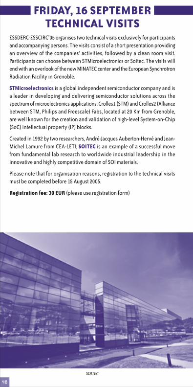
48
FRIDAY, 16 SEPTEMBERTECHNICAL VISITS
ESSDERC-ESSCIRC’05 organises two technical visits exclusively for participantsand accompanying persons. The visits consist of a short presentation providingan overview of the companies' activities, followed by a clean room visit.Participants can choose between STMicroelectronics or Soitec. The visits willend with an overlook of the new MINATEC center and the European SynchrotronRadiation Facility in Grenoble.
STMicroelectronics is a global independent semiconductor company and isa leader in developing and delivering semiconductor solutions across thespectrum of microelectronics applications. Crolles1 (STM) and Crolles2 (Alliancebetween STM, Philips and Freescale) Fabs, located at 20 Km from Grenoble,are well known for the creation and validation of high-level System-on-Chip(SoC) intellectual property (IP) blocks.
Created in 1992 by two researchers, André-Jacques Auberton-Hervé and Jean-Michel Lamure from CEA-LETI, SOITEC is an example of a successful movefrom fundamental lab research to worldwide industrial leadership in theinnovative and highly competitive domain of SOI materials.
Please note that for organisation reasons, registration to the technical visitsmust be completed before 15 August 2005.
Registration fee: 30 EUR (please use registration form)
SOITEC
P R O G R A M M E E S S C I R C
www.esscirc2005.com
31sh European Solid-State Circuits Conference12 - 16 September 2005 - Grenoble, France
Organized by
Technical Co-Sponsorship
CNRS-INPG-UJF
IEEE SOLID-STATECIRCUITS SOCIETY
SPONSORSThank you to our generous sponsors:
Soitec
SAMSUNG ADVANCEDINSTITUTE OF TECHNOLOGY

TUESDAY, 13 SEPTEMBER 200508:45
Coffee Break (Salle de Réception)
SESSION 2.E. : Analog Signal Processing(Chartreuse)
Introduction and Paper Award 2004 (Dauphine)
11:25
09:15 - 09:55 Joint Plenary Session - R. Cavin (Dauphine)
11:00
Lunch Break (Salon les Ecrins)
15:00
12:45
ESSCIRC Plenary Session - L. Larson (Dauphine)
SESSION 3.E. : High Resolution Data Converters(Dauphine)16:00
Coffee Break (Alpes Congrès - exhibtion area)
17:00
15:40
RUMP SESSION: Where will the Revolutionary Solutions come from: Technology or Design? (Dauphine)
18:30 End of conference day
Welcome Reception (Musée de Grenoble)19:00
WEDNESDAY, 14 SEPTEMBER 200509:00 - 09:40
Coffee Break (Alpes Congrès - exhibtion area)
SESSION 4.E. : DSP Building Blocks(Dauphine)
Joint Plenary Session - M. Shur (Dauphine)
10:45
10:25
18:00 End of conference day
Gala Dinner19:00
Lunch Break (Salon les Ecrins)12:45
14:15 - 14:55 Joint Plenary Session - M. Thompson (Dauphine)
Coffee Break (Salle de Réception)16:00
SESSION 6.E. : Continuous Time Filters(Chartreuse)16:20
THURSDAY, 15 SEPTEMBER 200509:00 - 09:40
Coffee Break (Salle de Réception)
SESSION 8.E. : High Speed Optical Interfaces(Chartreuse)
Joint Plenary Session - C. Joachim (Dauphine)
11:05
10:45
18:00 End of conference day
Farewell Party19:30
Lunch Break (Salon les Ecrins)12:45
14:15 Presentation ESSDERC-ESSCIRC 2006 (Dauphine)
15:10 ESSCIRC Plenary Session - B. Gammel, S. Rüping (Dauphine)
SESSION 9.E. : Analog Circuits(Dauphine)16:10
17:40 Closing Session (Dauphine)
Coffee Break (Alpes Congrès - exhibtion area)15:50
SESSION 1.E. : DC/DC Converters(Chartreuse)10:00
14:15 - 14:55 Joint Plenary Session - E. Yablonovitch (Dauphine)
SESSION 1.F. :Amplifiers beyond 10 GHz(Belle étoile)
SESSION 1.G. : Synthesizer Building Blocks(Meije)
SESSION 2.F. : Short Range Communications(Belle étoile)
SESSION 2.G. : Low Power and High Performance Digital Circuits(Meije)
SESSION 3.F. : PLLs(Oisans)
SESSION 3.G. : Clocking and Synchronisation(Stendhal)
09:45 ESSCIRC Plenary Session - B. Nauta (Dauphine)
SESSION 5.E. : Ultra Wide Band(Chartreuse)15:00
SESSION 4.F. : RF Circuits(Oisans)
SESSION 4.G. : Amplifiers(Stendhal)
SESSION 5.F. : Sensor Interfaces(Belle étoile)
SESSION 5.G. : Test of Digital Circuits and Memory(Meije)
SESSION 5.H. : Linear High Voltage Circuits(Sept Laux)
SESSION 6.F. : Sensor Integration(Belle étoile)
SESSION 6.G. : Memory Circuits(Meije)
14:25 - 15:05 Joint Plenary Session - H. Stormer (Dauphine)
SESSION 7.E. : Analogue Circuits for Communications(Chartreuse)09:45 SESSION 7.F. : VCOs
(Belle étoile)SESSION 7.G. : Crypto Systems
(Meije)SESSION 7.H. : Imagers 1
(Sept Laux)
SESSION 8.F. : Oversampled Data Converters(Belle étoile)
SESSION 8.G. : Digital Power Supply & Wiring(Meije)
SESSION 8.H. : Imagers 2(Sept Laux)
SESSION 9.F. : Cellular Communications(Oisans)
SESSION 9.G. : High Speed ADCs(Stendhal)
1
The 31st European Solid-State Circuits Conference takes place in Grenoblefrom Tuesday 13 September to Thursday 15 September 2005. The aim of theconference is to provide an annual European forum for the presentation anddiscussion of recent advances in solid-state circuit design and integration.ESSCIRC 2005 is jointly organized with the 35th European Solid-State DeviceResearch Conference (ESSDERC). The initiative to merge the two sisterconferences was started in 2002, as an incentive to foster the necessaryinteraction among technologists, device experts, and circuit & system designers.
While keeping separate Technical Programme Committees, ESSDERC andESSCIRC are governed by a single Steering Committee and share plenarykeynote presentations, tutorials (September 12) and satellite workshops(September 16) bridging both communities. Participants registered for eitherconference are encouraged to attend any of the scheduled parallel sessions.
ESSDERC-ESSCIRC is the largest and best quality European meeting related tomicro and nano electronics. In order to guarantee the excellence of the scientificlevel, the Steering Committee has imposed a very strict acceptance rate (40%).The evaluation of submitted papers has also been improved and newfunctionalities enabled in the web submission system. A total number of 288papers were submitted to ESSCIRC, representing a positive trend. More than30 countries, from all continents, were represented with substantialparticipations from Europe, USA, Japan and Korea. The final programme ofESSCIRC 2005 includes 119 contributions with outstanding plenary and sessioninvited talks. ESSCIRC 2005 covers all areas of integrated circuit design: analogand RF circuits, data converters, digital circuits, DSP and memories, mixed-signal circuits, imagers, sensors, systems-on-chip, advanced design conceptsand revolutionary architectures.
Several innovations are introduced this year in Grenoble: a joint panel session,session invited talks, paper exchange with DATE, an exhibit and technical visits(Friday September 16). Our conference has a new logo. A Special Issue of theJournal of Solid-State Circuits will contain selected full-length papers. Grenoblewill not miss the opportunity to preserve and develop the tradition of a warmSocial Programme: the Welcome Reception at the Museum of Grenoble (Tuesdayevening), the Gala Dinner and Show on Wednesday evening and, finally, theFarewell Party (Thursday evening) at the scenic Bastille location which overlooksGrenoble area and mountains. The accompanying persons will enjoy severalexcursions. Grenoble is a high-tech city, with wonderful surroundings in theheart of the Alps, offering attractive opportunities for an extended stay overthe weekend.
We would like to thank the authors for their contributions, the members ofthe Technical Programme Committee, Steering Committee and Local OrganizingCommittee for their hard work, Mrs Iris Mazuré our omnipresent conferencesecretary, and our generous sponsors.
We are looking forward to a successful conference, with exciting scientificcontents and rich human interactions. We warmly welcome you and yourcolleagues in Grenoble.
Sorin Cristoloveanu, Conference ChairMichel Brillouët, Conference Co-ChairAndreas Kaiser, ESSCIRC Technical Programme Chair
WELCOME

2
CONFERENCE ORGANISATION
COMMITTEES
GENERAL INFORMATION
CONFERENCE SITE
CONFERENCE REGISTRATION
CONFERENCE INFORMATION
SOCIAL PROGRAMME
ACCOMPANYING PERSONS PROGRAMME
EXHIBITORS
TECHNICAL VISITS
MAP CONFERENCE FACILITIES
ESSDERC-ESSCIRC JOINT PLENARY TALKS
MONDAY, 12 SEPTEMBER SHORT COURSES
TUESDAY, 13 SEPTEMBER SCIENTIFIC PROGRAMME
WEDNESDAY, 14 SEPTEMBER SCIENTIFIC PROGRAMME
THURSDAY, 15 SEPTEMBER SCIENTIFIC PROGRAMME
FRIDAY, 16 SEPTEMBER WORKSHOPS
NOTES
page(s)
3
4 - 5
6
6
6
6
6
6
6
6
7 - 8
9 - 14
15 - 16
17 - 23
24 - 31
32 - 39
40 - 47
48
TABLE OF CONTENTS
3
09Giant C2005 nanotubes in Grenoble.
CONFERENCE ORGANISATIONChairs
Sorin CristoloveanuGeneral [email protected]. +33 (0) 476 85 60 40
Michel BrillouëtCo-General [email protected]. +33 (0) 438 78 43 02
Andreas KaiserESSCIRC Technical Programme [email protected]. +33 (0) 320 30 40 43
Further information
For further information about the conference please contact the conferencesecretariat:
Iris Mazuré EspejoIMEP/ENSERG23 rue des Martyrs, BP 257,38016 Grenoble cedex 1, [email protected]. +33 (0) 476 85 60 76Fax +33 (0) 476 85 60 70
Or visit the web page: http://www.esscirc2005.com

4
Technical programme committeeAndrea Baschirotto University of Lecce (I)Eric Belhaire IEF - CNRS - University of Paris Sud (F)Didier Belot ST Microelectronics (F)Ivo Bolsens Xilinx SJ (USA)Werner Brockherde Fraunhofer IMS (D)Erik Bruun Technical University of Denmark (DK)Klaas Bult Broadcom Netherlands (NL)Herman Casier AMIS (B)Rinaldo Castello University of Pavia (I)Andreia Cathelin ST Microelectronics (F)Sudipto Chakraborty Texas Instruments (USA)Anantha Chandrakasan Massachusetts Institute of Technology (USA)Jan Crols AnSem (B)Wim Dehaene Katholieke Universiteit Leuven (B)Yann Deval IXL - University of Bordeaux (F)Stephane Donnay IMEC (B)Christian Enz CSEM (CH) - TPC Vice-ChairGeorges Gielen Katholieke Universiteit Leuven (B)Guiseppe Gramegna ST Microelectronics (I)Herbert Grünbacher Vienna Univ. of Technology (A)Christoph Hagleitner IBM Research - Zürich Research Laboratory (CH)Kari Halonen Helsinki Univ. of Technology (FIN)Ralph Hasholzner Freescale (D)Luis Hernandez Universidad Carlos III de Madrid (E)Qiuting Huang ETH Zurich (CH)David Johns University of Toronto (CDN)Volker Kempe Sensor Dynamics AG (A)Heinrich Klar Universität Berlin (D)Masaru Kokubo Hitachi (JP)Wieslaw Kuzmicz Warswa University of Technology (PL)Per Larsson-Edefors Chalmers University of Technology (CTH), Gothenburg (S)Domine Leenaerts Philips Research Laboratories (NL)John Long Technical University of Delft (NL)Damien Macq AMIS (B)Piero Malcovati University of Pavia (I)Franco Maloberti University of Pavia (I)Yiannos Manoli University of Freiburg (D)Sven Mattisson Ericsson Mobile (S)Peter Mole INTERSIL / Elantec Semiconductor (UK)Dominique Morche CEA/LETI (F)Michael Moyal Consultant (D)Sreedhar Natarajan Emerging Memory Technologies (CDN)Bram Nauta University of Twente (NL)Tobias Noll University of Technology RWTH Aachen (D)Olivier Nys Advanced Silicon SA (CH)Hakan Olsson Royal Institute of Technology (S)Yannis Papananos National Technical University of Athens (GR)Wolfgang Pribyl Austria Mikro Systeme International(A)Marcel Profirescu EDIL Microelectronics R&D Center (R)Manfred Punzenberger Infineon Technologies Austria AG (A)Ulrich Ramacher Infineon Technologies (D)
COMMITTEES
5
Bill Redman-White Philips Semiconductors /Southampton University (UK)Marc Renaudin TIMA - INPG Grenoble (F)Michel Rivier IBM France (F)Angel Rodriguez-Vazquez University of Sevilla (E)Arthur van Roermund Eindhoven University of Technology (NL)Albrecht Rothermel Universität Ulm (D)Stefan Rusu Intel Corporation (USA)Willy Sansen Katholieke Universiteit Leuven (B)Doris Schmitt-Landsiedel Technical University Munich (D)Patrice Senn France Telecom R&D (F)Joannes Sevenhans Consultant (B)Tadashi Shibata The University of Tokyo (JP)Werner Simbuerger Infineon Technologies (D)Michiel Steyaert Katholieke Universiteit Leuven (B)Stanislaw Szczepanski Gdansk University of Technology (PL)Hannu Tenhunen Royal Institute of Technology (S)Albert Theuwissen Dalsa (NL)Marc Tiebout Infineon Technologies (D)Janez Trontelj University of Ljubljana (SLO)Harry Veendrick Philips Research Laboratories (NL)Andreas Wiesbauer Infineon Technologies Austria AG (A)Horst Zimmermann TU Wien (A)
ESSDERC-ESSCIRC Steering committeeWerner Weber (Chair) Infineon Corporate Research (D)Giorgio Baccarani (Vice-Chair) University of Bologna (I)Peter Ashburn University of Southampton (UK)Cor Claeys IMEC (B)Sorin Cristoloveanu IMEP (F)Franz Dielacher Infineon Technologies Austria (A)Christian Enz CSEM (CH)José Epifanio da Franca Chipidea Microelectrónica (POR)Ernesto Perea STMicroelectronics (F)Hans-Jörg Pfleiderer University of Ulm (D)William Redman-White Philips Semiconductors (UK)Christer Svensson University of Lingköping (S)Reinout Woltjer Philips Research (NL)
ESSDERC-ESSCIRC Local organising committeeRaphaël Clerc IMEP-INPG (F)Simon Deleonibus CEA LETI (F)Denis Duret CEA LETI (F)Laurent Fesquet TIMA - INPG (F)Gérard Ghibaudo IMEP - INPG (F)Jalal Jomaah IMEP - INPG (F)Iris Mazurè IMEP - INPG (F)Laurent Montes IMEP - INPG (F)Mehdi Moussavi CEA LETI (F)Frédéric Petrot TIMA/SLS - INPG (F)Marc Renaudin TIMA - INPG (F)Thomas Repellin AEPI (F)Patrice Senn France Telecom R&D (F)
COMMITTEES
6
The Exhibition includes major scientific publishers and suppliers ofequipment/software.See Programme ESSDERC, page 21 and 22
EXHIBITORS
Three tours available ...See Programme ESSDERC, page 17
ACCOMPANYING PERSONSPROGRAMME
Not to be missed ...See Programme ESSDERC, page 16
SOCIAL PROGRAMME
Guidelines for oral presentations, web service, ...See Programme ESSDERC, page 15
CONFERENCE INFORMATION
Fees for the Conference, Tutorials, Workshops, Tours, ...See Programme ESSDERC, page 13 and 14
CONFERENCE REGISTRATION
How to get there ...See Programme ESSDERC, page 9 and 10
CONFERENCE SITE
About Grenoble, hotels, visa, ...See Programme ESSDERC, page 7 and 8
GENERAL INFORMATION
Friday, 16 september: STMicroelectronics or SOITEC, MINATEC, etcSee Programme ESSDERC, page 48
TECHNICAL VISITS
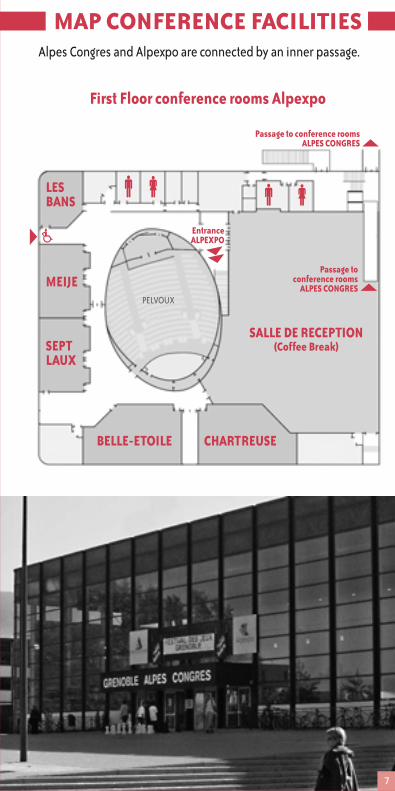
MAP CONFERENCE FACILITIESAlpes Congres and Alpexpo are connected by an inner passage.
First Floor conference rooms Alpexpo
BELLE-ETOILE
SEPTLAUX
CHARTREUSE
MEIJE
LESBANS
SALLE DE RECEPTION(Coffee Break)
EntranceALPEXPO
Passage toconference rooms
ALPES CONGRES
Passage to conference roomsALPES CONGRES
PELVOUX
7

8
MAP CONFERENCE FACILITIESGround Floor conference rooms Alpes Congrès
STENDHALINTERNET
AREA
BERLIOZ(Office)
BAYARD
To Dauphine and Oisans To Daupine Downstairs to lunch area (Salon Les Ecrins) To Oisans Speakers room Telephone
CONFERENCEREGISTRATION
Main entrance ALPES CONGRES
EXHI
BITI
ON
AN
D Co
ffee
BRE
AKS
First Floor conference rooms Alpes Congrès
DAUPHINE
Bar
OISANS
Passage to Alpexpo Downstairs to Conference Registration, Exhibition & Coffe Break
LESDIGUIERES
ESSDERC-ESSCIRCJOINT PLENARY TALKS
9
Horst Stormer“Silicon Forever! Really?”
With certainty scaling in silicon is going to hit a wall, technologically oreconomically. While we don't know exactly when this is going to happen,"approximately a decade from now" is a pretty common guess. Hence it isprudent to imagine and investigate alternative ways to create electronic systemsthat may have a chance to lead us "beyond silicon". At present there is no clearpath at all. Only open-minded and imaginative research has a chance toovercome the foreseeable impasse. One of these "crazy ideas" may just panout; just like using semiconductors instead of vacuum tubes or the printing ofinterconnects instead of using copper wires.
Biography
Horst Stormer received his Ph.D. in 1977 from the University of Stuttgart andjoined Bell Labs as a postdoc shortly after. From 1983 to 1992 he headed theSemiconductor Physics Research Department and became the Director of thePhysical Research Laboratory of AT&T Bell Labs in 1992. In 1997 Stormer movedto Adjunct Physics Director at Bell Labs and became a Professor in the Physicsand the Applied Physics Department of Columbia University in New York.Stormer has worked extensively on the properties of lower-dimensionalelectron systems and is one of the Scientific Directors of the Columbia NSFNano Center. H. Stormer received the Nobel Prize in Physics in 1998.
Eli Yablonovitch“Silicon Nano-Photonics: Where the Photons Meet the Electrons”
It has become apparent that silicon technology can provide many of therequirements for nanophotonic integration, including many of the commondiscrete opto-electronic components. Some of these components are based onphotonic crystal designs, but generally electromagnetic design becomes themain research requirement in nano-photonics. The question has always beenwhat is the exact structure that should be fabricated? The era of purely intuitivedesign may be obsolete.
We must now concentrate more on design software, rational design, and thenumerical solution of inverse problems. There are a number of inverse algorithms,including genetic algorithms, the errorpropagation method, and simulatedannealing that can contribute to future progress in nanophotonic design.
Biography
Eli Yablonovitch graduated with the Ph.D. degree in Applied Physics from HarvardUniversity in 1972. He worked for two years at Bell Telephone Laboratories, andthen became a Professor of Applied Physics at Harvard. In 1979 he joined Exxonto do research on photovoltaic solar energy. Then in 1984, he joined Bell
10
ESSDERC-ESSCIRCJOINT PLENARY TALKS
Communications Research, where he was a Distinguished Member of Staff, andalso Director of Solid-State Physics Research. In 1992 he joined the Universityof California, Los Angeles, where he is Professor of Electrical Engineering. He isa Fellow of the Institute of Electrical and Electronic Engineers, the Optical Societyof America, and the American Physical Society. Yablonovitch is a Life Memberof Eta Kappa Nu, and a Member of the National Academy of Engineering andthe National Academy of Sciences.
Michael Shur“Terahertz Electronics: Devices, Circuits, and Applications”
Transistors with nanometer critical feature sizes, such as HBTs and HEMTs, relyingon ballistic transport in semiconductors with small electron effective massesand on innovative designs minimizing parasitics, are penetrating the subterahertzrange, still being dominated by two terminal devices. New ideas of using plasmaresonances for tunable detection and emission of terahertz radiation are beingexplored. Plasma effects in polarization-induced electrons and holes in 2D and1D pyroelectric heterostructures hold promise of an active THz medium. Thedevelopment of tunable solid state monolithically integrated THz sources anddetectors based on these approaches will enable many applications rangingfrom detection of biological hazardous agents and explosives to medicaldiagnostics, contactless in-situ testing of integrated circuits, and applications inspectroscopy, radioastronomy and environmental control.
Biography
Michael Shur received his M. S. E. E. degree (with honors) from LETI in 1965, Ph.D. in Physics from A. F. Ioffe Institute in 1967 and Doctor of Science degree fromA. F. Ioffe in 1992. He is now Patricia W. and C. Sheldon Roberts'48 Professor ofSolid State Electronics, Professor of Physics, and Director of Broadband DataTransport Center at Rensselaer Polytechnic Institute. He is a Fellow of IEEE, ofAmerican Physical Society, and of ECS and a member of Eta Kappa Nu, Sigma Xi,Tau Beta Pi, ASEE, and Humboldt Society of America. Dr. Shur is Editor-in-Chiefof IJHSES and of the book series on Special Topics in Electronics and Systems.
Ralph Cavin“Limits of CMOS Devices and Circuits”
Current CMOS devices operate at about six orders of magnitude above thekTln(2) joules/bit switching limit imposed by physics. Nevertheless, it can beshown that continued scaling of device features that are then densely packedand operated at attainable frequencies will result in the generation of thermalloads that cannot be managed by any known heat removal technology. Wediscuss possible successor/complementary logic devices that reduce the level
11
ESSDERC-ESSCIRCJOINT PLENARY TALKS
of heat generation and we especially focus on new non-volatile memorytechniques that could radically impact information processing architecturesand hence the performance requirements for logic devices.
Biography
Dr. Cavin received his BSEE (1961) and MSEE (1962) from Mississippi StateUniversity and his PhD in Electrical Engineering from Auburn University in 1968.He served as a Senior Engineer at the Martin-Marietta Company in Orlando,Florida from 1962 -1965. At Martin, Dr. Cavin was involved in the design andmanufacture of missile guidance and control systems. After taking his Ph.D., Dr.Cavin joined the Department of Electrical Engineering at Texas A & M Universitywhere he obtained the rank of Full Professor and also served the departmentas Assistant Head for Research. In 1983, he joined the Semiconductor ResearchCorporation where he served as Director of Design Sciences research programsuntil 1989. He became Head of the Department of Electrical and ComputerEngineering at North Carolina State University from 1989 - 1994 and was Deanof Engineering at North Carolina State University from 1994 - 1995. He is currentlyVice President for Research Operations at the Semiconductor ResearchCorporation.
Mike Thompson“Future of CMOS Technology, Manufacturing and Products”
Over the last couple of years, there has been a shift away from the traditionalsituation where CMOS IC designs and their applications were being limited intheir scope by the capability of the available manufacturing technology. Thejump to 300mm manufacturing at 90nm and below seems to be turning thisphenomenon on its head by offering staggering integration densities andmassive production capacities that are becoming much more difficult fordesigners to exploit due to the shear complexity of the product and applicationdevelopments. In this talk, we will review some of the likely adaptations ofthe present design and manufacturing approaches that will allow the gap tobe closed.
Biography
Mike Thompson was born in Glasgow, Scotland, in 1957. After graduating fromthe University of Glasgow with a Bsc Hons in Astronomy with AdvancedMathematics, he started working in 1980 at General Instrument Microelectronicsat Glenrothes (Scotland) as a Photolithography Engineer. In 1982, he joinedInmos Ltd at Newport (South Wales, UK), a 100mm wafer fab specialising inhigh performance memories and microprocessors, that was acquired in 1989to become SGS-THOMSON Ltd, where he worked until 1991 as ProcessDevelopment Manager and Engineering Manager. Then in 1991, he left the UK

12
ESSDERC-ESSCIRCJOINT PLENARY TALKS
for France, to work at STMicroelectronics Crolles, ST's first 200 mm wafer fab,where he was appointed Operations Director. Mike Thompson was involvedin the first process technology development collaboration betweenSTMicroelectronics and Philips from its start in 1992, as well as in the creationof the STMicroelectronics-France Telecom-CEA/Leti Centre Commun. Today,he has the double responsibility of managing the 200mm wafer fab andcontributing to the start-up of Crolles 2, the new 300mm state-of-the-art facility,specialising in high performance technologies for system-on-chip.
Christian Joachim“Towards a Molecule - Computer? ”
There is another world down where miniature machines do not result from aminiaturisation process but from the monumentalisation of the molecularstructure. What about assembling machines atom by atom, and stopping atthe minimum number of atoms required for the machine to compute, carry,and communicate...? We will present the design of the first prototype of uni-molecular moleculemachines like a wheelbarrow, a Morse manipulator, aWheatstone bridge, an OR and AND intramolecular logic gate and an atomicwire mould. Some experimental results will be given. Then, we discuss thenext step: the design of very complex machines like a full computing unitintegrated inside a single molecule.
Biography
Dr. Christian Joachim is Director of Research at CNRS and head of the molecularNanoscience and Picotechnology group in CEMES/CNRS, Toulouse. His recentaccomplishments are the theory of atomic and molecular manipulation withthe STM, the discovery of long range tunnel processes through a molecule, thefabrication of metal-insulator-metal planar nanojunctions for the planarimplementation of molecular devices and the discovery of the first molecularrotor. More recently, he introduced the concept of mono-molecular electronics,of tunnel wired molecular nano-robots with the design of the first molecularwheelbarrow and is now developing atomic scale technology. He is the authorof more than 170 scientific publications and has presented more than 180talks. Dr. Joachim received the 1988 French Chemical Physics Prize for his workon electron transfer theory, the 1991 IBM France Prize for his work on tunnellingthrough a molecule and the 1997 Feynman Prize "experimental" for his workon molecular manipulation. In 1999, he received the French NanotechnologyPrize for his work on nanoscale science and the Share University ResearchAward of IBM for his work on intramolecular circuits. In 2002, he received fromthe CNRS, the Silver Medal in Chemistry for his work on molecular nanosciences.
13
ESSCIRC-INVITEDPLENARY TALKS
Lawrence E. Larson“Digital control of RF power amplifiers for next generation wireless
communications”
Future generations of wireless communications are expected to place increasingburdens on the efficiency and linearity of power amplifiers, due to the use ofmore complex waveforms and OFDM. This has implications for the design oftransmitters in portable/mobile devices as well as base stations and accesspoints. Although semiconductor device technology has made rapid progress infundamental power amplifier transistor performance, the use of digital signalprocessing techniques to optimize the linearity and efficiency provides enormouspotential for further improvement (especially on the handset side). This paperwill summarize the digital techniques that can be employed to improve theperformance of wireless power amplifiers.
Biography
Lawrence E. Larson is currently Director of the UCSD Center for WirelessCommunications and the Communications Industry Professor of Electrical andComputer Engineering at the University of California, San Diego. He is therecipient or co-recipient of numerous awards including the 1996 Lawrence A.Hyland Patent Award of Hughes Electronics, for his work on low-noisemillimeterwave HEMTs, and the 1999 IBM Microelectronics Excellence Awardfor his work in Si/SiGe HBT technology. He has published over 200 papers, co-authored three books, has received 27 US patents, and is a Fellow of the IEEE.
Bram Nauta“Analog/RF circuit design techniques for nanometerscale IC technologies”
CMOS evolution introduces several problems in analog design. Gate-leakagemismatch exceeds conventional matching tolerances requiring active cancellationtechniques or alternative architectures. One strategy to deal with the use oflower supply voltages is to operate critical parts at higher supply voltages, byexploiting combinations of thin- and thick-oxide transistors. Alternatively lowvoltage circuit techniques are successfully developed. In order to benefit fromnanometer scale CMOS technology, more functionality is shifted to the digitaldomain, including parts of the RF circuits.
Biography
Bram Nauta received the M.Sc degree (1987) and the Ph.D. degree (1991) inelectrical engineering from the University of Twente, Enschede, The Netherlands.In 1991 he joined the Mixed-Signal Circuits and Systems Department of PhilipsResearch, Eindhoven the Netherlands, where he worked on various analogbaseband circuits. In 1998 he returned to the University of Twente, as fullprofessor heading the IC Design group in the MESA+ Research Institute anddept. of Electrical Engineering. His current research interest is high speed analogCMOS circuits for transceivers.
14
ESSCIRC-INVITEDPLENARY TALKS
Stefan Rüping and Berndt Gammel“SmartCards inside”
Today's SmartCard- and Security-IC's are not only phone cards anymore, theyare embedded cryptographic security processors and have to face specialchallenges concerning architecture, design, methodology and technology. Therequirements for power and performance are extremely contradictory. On theone hand, embedded Java capability needs the high performance computingpower of a 32bit core including caches. On the other hand the contactlessoperation mode requires ultra low power ability. SmartCard IC's have specificco-processors for efficient cryptographic execution and a bunch of peripheralsto enable a flexible use of the controller for many kinds of applications. SecurityIC's are subject to attacks. An overview of invasive and non-invasive attacksand also examples for appropriate countermeasures will be given. Exciting futuretrends will be presented furthermore.
Biographies
Stefan Rüping obtained his Dipl.-Ing. and his Dr.-Ing. in electrical engineeringfrom Dortmund University/Germany. From 1995 to 2000, he was a senior engineerat the Heinz Nixdorf Institute, Paderborn/Germany, doing research on conceptsand ASICs for decentralized intelligent systems and artificial neural networks.Since November 2000 he is working on innovations and concepts for high securitysystem and hardware solutions within the Secure Mobile Solutions (SMS)department of Infineon. He is head of the concept engineering group responsiblefor 8/16 bit smartcard controllers.
Berndt M. Gammel obtained his Dipl. Phys. and his Dr. rer. nat. from TechnischeUniversität München. Since 1998 he is working on microprocessor architectures,concepts and innovations for high security system and hardware solutionswithin the Security and Chip Card ICs department of Infineon Technologies AG.He is the head of the concept engineering group responsible for the 32 bitsmartcard controller family.
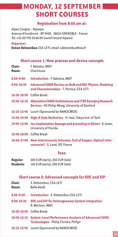
15
MONDAY, 12 SEPTEMBERSHORT COURSESRegistration from 8:00 am at :
Alpes Congres - AlpexpoAvenue d'Innsbruck - BP 2408 - 38034 GRENOBLE - FranceTel. +33 (0) 476 39 66 00 (switch board Alpexo)
Organiser:Simon Deleonibus CEA-LETI, email: [email protected]
Short course 1: New process and device conceptsChair: F. Balestra, IMEPRoom: Chartreuse
8:50-9:00 Introduction - F. Balestra, IMEP
9:00-10:30 Advanced CMOS Devices on Bulk and SOI: Physics, Modelingand Characterisation - T. Poiroux, CEA LETI
10:30-10:45 Coffee Break
10:45-12:15 Alternative CMOS Architectures and ITRS Emerging ResearchDevices - HS Philip-Wong, University of Stanford
12:15-13:45 Lunch (Sponsored by NANOCMOS)
13:45-14:45 High-K Gate Dielectrics - H. Iwai, Tokyo Inst. of Tech
14:45-15:45 Ion Implantation Damage and Annealing in Silicon - K. Jones,University of Florida
15:45-16:00 Coffee Break
16:00-17:00 New Interconnects Schemes: End of Copper, Optical Inter-connects? - S. Laval, IEF, France
Fees:
Regular: 200 EUR (early), 250 EUR (late)Students: 150 EUR (early), 200 EUR (late)
Short course 2: Advanced concepts for SOC and SIPChair: S. Deleonibus, CEA-LETIRoom: Belle étoile
8:50-9:00 Introduction - S. Deleonibus CEA-LETI
9:00-10:30 SOC and SIP for Heterogeneous System Integration -R. Mertens, IMEC
10:30-10:45 Coffee Break
10:45-12:15 System-Level Performance Analysis of Advanced CMOSTechnologies - Philip Christie, Philips
12:15-13:45 Lunch (Sponsored by NANOCMOS)

16
MONDAY, 12 SEPTEMBER13:45-14:45 Advanced SiGeC BICMOS Technology for SoC Integration -
A. Chantre, STMicroelectronics
14:45-15:45 Embedded Memories - A. Maurelli, STMicroelectronics
15:45-16:00 Coffee Break
16:00-17:00 Introducing New Devices on Chip: MEMS, Sensors, etc. -P. Ancey, STMicroelectronics
Fees:Regular: 200 EUR (early), 250 EUR (late)Students: 150 EUR (early), 200 EUR (late)
Short course 3: Nanoelectronics - Beyond the roadmapEmerging research devices
Chair: G. Baccarani, Univ. BolognaRoom: Meije
8:50-9:00 Introduction - G. Baccarani, Univ. Bologna
9:00-10:00 Molecular Electronics: Self-Assembly and Organisation,Carbon Nanotubes - J-P. Bourgoin, CEA
10:00-11:00 Spin Electronics - C. Chappert, IEF
11:00-11:15 Coffee Break
11:15-12:15 Quantum Computing in Quantum Dots - D. Loss, U. Basel
12:15-13:45 Lunch (Sponsored by NANOCMOS)
Short course 4: Emerging Memory ArchitecturesWhen will the UNIversal Memory be available?
Chair: R. Bouchakour, Univ. MarseilleRoom: Meije
12:15-13:45 Lunch (Sponsored by NANOCMOS)
13:50-14:00 Introduction - R. Bouchakour, Univ. Marseille
14:00-15:00 Technology and Key Design Issues for New Memory Devices(Embedded and Stand Alone) - Kinam Kim, Samsung
15:00-16:00 FeRAM and MRAM Technologies - Y. Arimoto, Fujitsu
16:00-16:15 Coffee Break
16:15-17:15 New Memory Concepts: from Silicon Nanocrystal Memoriesto Molecular Memories - B. De Salvo, LETI
Fees (short course 3 + 4):Regular: 200 EUR (early), 250 EUR (late)Students: 150 EUR (early), 200 EUR (late)

17
TUESDAY, 13 SEPTEMBERSCIENTIFIC PROGRAMME
Introduction and Paper Award 2004Time: 08:45 - 09:15Location: Dauphine
Joint Plenary SessionChairs: S. Cristoloveanu, IMEP (France) ; M. Brillouët, CEA-LETI (France)Time: 09:15 - 09:55Location: Dauphine
09:15 Future Devices for Information ProcessingR. Cavin, V. Zhirnov, Semiconductor Research Corporation, USA
SESSION 1.E. : DC/DC ConvertersChairs: H. Casier, AMIS (Belgium) ; M. Moyal, Consultant (Germany)Time: 10:00 - 11:00Location: Chartreuse
1E110:00 A PMOS-Switch Based Charge Pump Allowing Low Cost
Implementation on a CMOS Standard ProcessE. Racape, J. Daga, Atmel, France
1E210:20 A PWM Dual-Output DC/DC Boost Converter in a 0.13um CMOS
Technology for Cellular-Phone Backlight ApplicationS. Kuok Hoon, N. Culp, Texas Instruments, USA; J. Chen, AdvancedAnalogic Tech, USA; F. Maloberti, University of Pavia, Italy
1E310:40 A New Integrated Charge Pump Architecture Using Dynamic
Biasing of Pass TransistorsL. Mensi, L. Colalongo, A. Richelli, Z. Kovacs, University of Brescia,Italy
SESSION 1.F.: Amplifiers beyond 10 GHzChairs: Y. Papananos, National Technical University of Athens (Greece);
S. Chakraborty, Texas Instruments (USA)Time: 10:00 - 11:00Location: Belle étoile
1F110:00 24 GHz LNA in 90nm RF-CMOS with High-Q Above-IC Inductors
O. Dupuis, X. Sun, G. Carchon, P. Soussan, IMEC, Belgium; M. Frendahl,Chalmers University of Technology, Sweden; S. Decoutrer, W. DeRaedt, IMEC, Belgium

18
TUESDAY, 13 SEPTEMBER1F210:20 A 28.5GHz Monolithic Cascode LNA with 70GHz fT SiGe HBTs
F. Fortes, J. Freire, Instituto de Telecomunicações, Portugal;D. Leenaerts, Philips Research, The Netherlands; R. Mahmoudi,A. Roermund, Technische Universiteit Eindhoven, The Netherlands
1F310:40 A 12.5GHz SiGe BICMOS Limiting Amplifier Using a Dual Offset
Cancellation LoopA. Maxim, Maxim, USA; D. Antrik, University of Texas at Austin, USA
SESSION 1.G. : Synthesizer Building BlocksChairs: M. Tiebout, Infineon Technologies (Germany) ; J. Crols, AnSem
(Belgium)Time: 10:00 - 11:00Location: Meije
1G110:00 GMSK Modulation of Subharmonic Injection Locked Oscillators
T. Finateu, STMicroelectronics, France; Y. Deval, IXL, France; F. Badets,STMicroelectronics, France; J. Begueret, IXL, France
1G210:20 Phase Noise Degradation of LC-tank VCOs Due to Substrate
Noise and Package CouplingM. Méndez, D. Mateo, X. Aragonès, J. González, Electronic EngineeringDepartment, UPC, Spain
1G310:40 A 34GHz/1V Prescaler in 90nm CMOS SOI
M. Sanduleanu, Philips Research Eindhoven, The Netherlands;R. Ionita, Institut Superieur d'Electronique de Paris - ISEP, France;A. Vladimirescu, University of California at Berkeley, BWRC, USA
Coffee BreakTime: 11:00 - 11:20Location: Salle de Réception
SESSION 2.E. : Analog Signal ProcessingChairs: H. Grünbacher, Vienna Univ. of Technology (Austria) ; S. Donnay,
IMEC (Belgium)Time: 11:25 - 12:45Location: Chartreuse
2E111:25 Continuous-Time DSPs, Analog/Digital Computers and Other
Mixed-Domain Circuits (Invited)Y. Tsividis, G. Cowan, Y. Li, K. Shepard, CISL, Department of ElectricalEngineering, Columbia University, USA
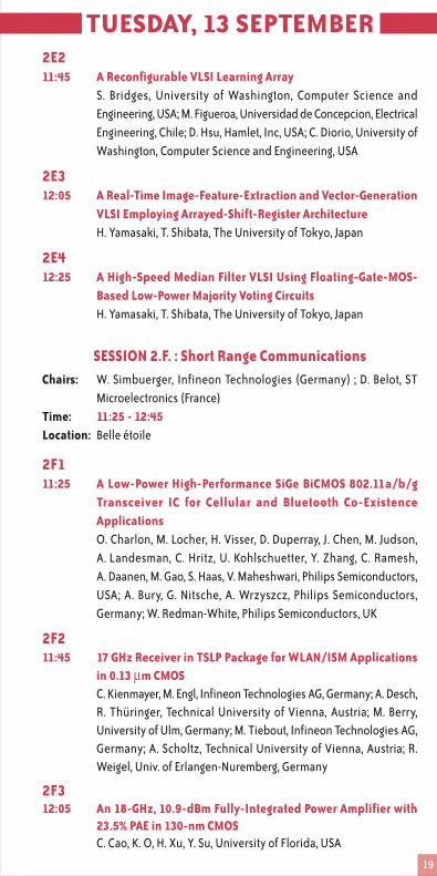
19
TUESDAY, 13 SEPTEMBER2E211:45 A Reconfigurable VLSI Learning Array
S. Bridges, University of Washington, Computer Science andEngineering, USA; M. Figueroa, Universidad de Concepcion, ElectricalEngineering, Chile; D. Hsu, Hamlet, Inc, USA; C. Diorio, University ofWashington, Computer Science and Engineering, USA
2E312:05 A Real-Time Image-Feature-Extraction and Vector-Generation
VLSI Employing Arrayed-Shift-Register ArchitectureH. Yamasaki, T. Shibata, The University of Tokyo, Japan
2E412:25 A High-Speed Median Filter VLSI Using Floating-Gate-MOS-
Based Low-Power Majority Voting CircuitsH. Yamasaki, T. Shibata, The University of Tokyo, Japan
SESSION 2.F. : Short Range CommunicationsChairs: W. Simbuerger, Infineon Technologies (Germany) ; D. Belot, ST
Microelectronics (France)Time: 11:25 - 12:45Location: Belle étoile
2F111:25 A Low-Power High-Performance SiGe BiCMOS 802.11a/b/g
Transceiver IC for Cellular and Bluetooth Co-ExistenceApplicationsO. Charlon, M. Locher, H. Visser, D. Duperray, J. Chen, M. Judson,A. Landesman, C. Hritz, U. Kohlschuetter, Y. Zhang, C. Ramesh,A. Daanen, M. Gao, S. Haas, V. Maheshwari, Philips Semiconductors,USA; A. Bury, G. Nitsche, A. Wrzyszcz, Philips Semiconductors,Germany; W. Redman-White, Philips Semiconductors, UK
2F211:45 17 GHz Receiver in TSLP Package for WLAN/ISM Applications
in 0.13 µm CMOSC. Kienmayer, M. Engl, Infineon Technologies AG, Germany; A. Desch,R. Thüringer, Technical University of Vienna, Austria; M. Berry,University of Ulm, Germany; M. Tiebout, Infineon Technologies AG,Germany; A. Scholtz, Technical University of Vienna, Austria; R.Weigel, Univ. of Erlangen-Nuremberg, Germany
2F312:05 An 18-GHz, 10.9-dBm Fully-Integrated Power Amplifier with
23.5% PAE in 130-nm CMOSC. Cao, K. O, H. Xu, Y. Su, University of Florida, USA
20
TUESDAY, 13 SEPTEMBER2F412:25 SiGe Transformer Matched Power Amplifier for Operation at
Millimeter-Wave FrequenciesU. Pfeiffer, IBM T.J. Watson Research Center, USA; D. Goren, IBM,Israel; B. Floyd, S. Reynolds, IBM T.J. Watson Research Center, USA
SESSION 2.G. :Low Power and High Performance Digital Circuits
Chairs: S. Rusu, Intel Corporation (USA) ; P. Larsson-Edefors, ChalmersUniversity of Technology (Sweden)
Time: 11:25 - 12:45Location: Meije
2G111:25 Dynamic State-Retention FlipFlop for Fine-Grained Sleep
Transistor Scheme
S. Henzler, Technical University of Munich, Germany; T. Nirschl,C. Pacha, Infineon Technologies, Germany; P. Teichmann, M. Eireiner,J. Fischer, Technical University of Munich, Germany; G. Georgakos,J. Berthold, Infineon Technologies, Germany; D. Schmitt-Landsiedel,P. Spindler, M. Fulde, T. Fischer, Technical University of Munich,Germany
2G211:45 Isodelay Output Driver Design using Step-wise Charging for
Low PowerA. Katoch, H. Veendrick, Philips Research Laboratories, TheNetherlands
2G312:05 Low Leakage Design Techniques for LUT-based FPGAs
A. Lodi, L. Ciccarelli, D. Loparco, University of Bologna, Italy; R.Canegallo, STMicroelectronics, Italy; R. Guerrieri, University ofBologna, Italy
2G412:25 An On-Chip Jitter Measurement Circuit with Sub-picosecond
ResolutionK. Jenkins, IBM T.J. Watson Research Center, USA; A. Jose, ColumbiaUniversity, USA; D. Heidel, IBM T.J. Watson Research Center, USA
LunchTime: 12:45 - 14:10Location: Les Ecrins

21
TUESDAY, 13 SEPTEMBERJoint Plenary Session
Chairs: M. Steyaert, Katholieke Universiteit Leuven (Belgium); W. Redman-White, Philips Semiconductors (UK)
Time: 14:15 - 14:55Location: Dauphine
14:15 Silicon Nano-Photonics: Where the Photons Meet the ElectronsE. Yablonovitch, Electrical Engineering Department, University ofCalifornia, USA
ESSCIRC Plenary SessionChairs: M. Steyaert, Katholieke Universiteit Leuven (Belgium); W. Redman-
White, Philips Semiconductors (UK)Time: 15:00 - 15:40Location: Dauphine
15:00 Digital Control of RF Power Amplifiers for Next-GenerationWireless CommunicationsL. Larson, P. Asbeck, D. Kimba, Center for Wireless Communications,University of California, USA
Coffee BreakTime: 15:40 - 16:00Location: Alpes Congrès
SESSION 3.E. : High Resolution Data ConvertersChairs: D. Macq, AMIS (Belgium) ; D. Johns, University of Toronto (Canada)Time: 16:00 - 17:00Location: Dauphine
3E116:00 A 15-bit 30 MS/s 145 mW Three-step ADC for Imaging
ApplicationsH. van der Ploeg, M. Vertregt, Philips Research, The Netherlands;M. Lammers, Philips ICLab, France
3E216:20 A 220mW 14b 40MSPS Gain Calibrated Pipelined ADC
J. Bjørnsen, Norwegian University of Science and Technology,Norway; Ø. Moldsvor, T. Sæther, Nordic Semiconductor ASA, Norway;T. Ytterdal, Norwegian University of Science and Technology, Norway
3E316:40 An On-chip Self-calibration Method for Current Mismatch in
D/A ConvertersG. Radulov, Eindhoven University of Technology, The Netherlands;P. Quinn, Xilinx, Ireland; H. Hegt, A. van Roermund, EindhovenUniversity of Technology, The Netherlands

22
TUESDAY, 13 SEPTEMBERSESSION 3.F. : PLLs
Chairs: J. Long, Technical University of Delft (The Netherlands) ; Q. Huang,ETH Zurich (Switzerland)
Time: 16:00 - 17:00Location: Oisans
3F116:00 A fast-hopping single-PLL 3-band UWB
R. van de Beek, D. Leenaerts, G. van der Weide, Philips Research,The Netherlands
3F216:20 Multi-Standard Carrier Generation System for Quad-band GSM
/ WCDMA (FDD-TDD) / WLAN (802.11 a-b-g) radioA. Koukab, Y. Lei, M. Declercq, Ecole Polytechnique Fédérale deLausanne (EPFL), Switzerland
3F316:40 Fast AFC Technique Using a Code Estimation and Binary Search
Algorithm for Wideband Frequency SynthesisK. Lee, E. Sung, I. Hwang, B. Park, Samsung Electronics, Korea
SESSION 3.G. : Clocking and SynchronisationChairs: W. Dehaene, Katholieke Universiteit Leuven (Belgium);
R. Hasholzner, Freescale (Germany)Time: 16:00 - 17:00Location: Stendhal
3G116:00 A Novel 40-GHz Flip-Flop-Based Frequency Divider in 0.18 µm
CMOSR. Mohanavelu, Intel, USA; P. Heydari, University of California, Irvine,USA
3G216:20 A Fast-Lock Mixed-Mode DLL with Wide-Range Operation and
Multiphase OutputsK. Cheng, Y. Lo, National Central University, Taiwan
3G316:40 A Multichannel 3.5mW/Gbps/Ch Gated Oscillator Based CDR
in a 0.18 µm Digital CMOS TechnologyA. Tajalli, EE dept, Sharif U of T, Iran; P. Muller, LSM, EPFL, Lausanne,Switzerland; M. Atarodi, EE dept, Sharif U of T, Iran; Y. Leblebici,LSM, EPFL, Lausanne, Switzerland
23
TUESDAY, 13 SEPTEMBER
Welcome Reception at the “Musée de Grenoble”
Time: 19:00
RUMP SESSION: Where will the revolutionary solutionscome from: technology or design?
Time: 17:00 - 18:30Location: Dauphine
Moderators : T. Skotnicki (STMicroelectronics, France) , A. Kaiser (IEMN, France)
ESSDERC Panelists : Hiroshi IWAI (Tokyo Institute of Technology, Japan) Rainer WASER (RWTH-Aachen, Germany) Kazunari ISHIMARU (SoC R&D Center, TOSHIBA Corp., Japan) Peter ZEITZOFF (SEMATECH, USA)
ESSCIRC Panelists: Clive BITTLESTONE (Texas Instruments, USA) Georges GIELEN (K.U. Leuven, Belgium) Sreedhar NATARAJAN (Emerging Memory Technologies, Canada) Yannis TSIVIDIS (Columbia University, USA)
This rump session brings together eight international experts intechnology/devices and advanced design. Each panelist represents adifferent area of the technology or design: from CMOS manufacturing andadvanced Si devices to nanoelectronics beyond CMOS, from analog & RFto memory and CAD. Short presentations are given to stimulate questionsand comments from the audience. What are the bottlenecks? What are theperspectives for breakthrough solutions? Will they come from thetechnology/device side, from the design side, or from both?
Grenoble & CMOS interconnects
24
WEDNESDAY, 14 SEPTEMBERSCIENTIFIC PROGRAMME
Joint Plenary SessionChairs: C. Enz, CSEM (Switzerland) ; E. Perea, STMicroelectronics (France)Time: 09:00 - 09:40Location: Dauphine
09:00 Terahertz Technology: Devices and ApplicationsM. Shur, ECSE Department and Broadband Center, RensselaerPolytechnic Institute, USA
ESSCIRC Plenary SessionChairs: C. Enz, CSEM (Switzerland) ; E. Perea, STMicroelectronics (France)Time: 09:45 - 10:25Location: Dauphine
09:45 Analog/RF Circuit Design Techniques for Nanometerscale ICTechnologiesB. Nauta, A. Annema, University of Twente, The Netherlands
Coffee Break (Sponsored by Mentor Graphics)
Time: 10:25 - 10:45Location: Alpes Congrès
SESSION 4.E. : DSP Building BlocksChairs: T. Noll, University of Technology RWTH Aachen (Germany) ;
M. Renaudin, TIMA - INPG Grenoble (France)Time: 10:45 - 12:45Location: Dauphine
4E110:45 Design for Manufacturing in the Nanoscale Era (Invited)
C. Bittlestone, Texas Instruments, USA
4E211:05 A 2GHz 13.6mW 12x9b Multiplier for Energy Efficient FFT
AcceleratorsS. Hsu, Intel Corporation, USA; V. Venkatraman, University ofMassachusetts, USA; S. Mathew, H. Kaul, M. Anders, S. Dighe, IntelCorporation, USA; W. Burleson, University of Massachusetts, USA;R. Krishnamurthy, Intel Corporation, USA
4E311:25 The Vector Fixed Point Unit of the Synergistic Processor Element
of the Cell Architecture ProcessorN. Mäding, IBM Entwicklung GmbH, Böblingen, Germany; J. Leenstra,J. Pille, R. Sautter, S. Büttner, S. Ehrenreich, W. Haller, IBM EntwicklungGmbH, Böblingen, Germany
25
WEDNESDAY, 14 SEPTEMBER4E411:45 A Fixed-Point Multimedia Co-Processor with 50Mvertices/s
Programmable SIMD Vertex Shader for Mobile ApplicationsJ. Sohn, J. Woo, KAIST, Korea; R. Woo, Texas Instruments Inc., Korea;H. You, KAIST, Korea
4E512:05 A 3.33Gb/s (1200,720) Low-Density Parity Check Code Decoder
C. Lin, K. Lin, H. Chang, C. Lee, DEE, National Chiao Tung University,Taiwan
4E612:25 ASIC Implementation of a MIMO-OFDM Transceiver for 192
Mbps WLANsD. Perels, S. Haene, P. Luethi, A. Burg, W. Fichtner, Integrated SystemsLaboratory, ETH Zurich, Switzerland; H. Bölcskei, CommunicationTechnology Laboratory, ETH Zurich, Switzerland; N. Felber, IntegratedSystems Laboratory, ETH Zurich, Switzerland
SESSION 4.F. : RF CircuitsChairs: D. Leenaerts, Philips Research Laboratories (The Netherlands); G.
Gramegna, ST Microelectronics (Italy)Time: 10:45 - 12:45Location: Oisans
4F110:45 ESD-protected CMOS 3-5 GHz Wideband LNA+PGA Design for
UWBR. Salerno, Infineon Technologies, Austria; M. Tiebout, H. Paule,M. Streibl, Infineon Technologies, Germany; C. Sandner, InfineonTechnologies, France; K. Kropf, Infineon Technologies, Germany
4F211:05 A 5-GHz BiCMOS Variable-Gain Low Noise Amplifier with
Inductorless Low-Gain BranchM. Liu, J. Craninckx, IMEC vzw, Belgium
4F311:25 A Cellular-Band CDMA 0.25 µm CMOS LNA Linearized using
Active Post-DistortionN. Kim, V. Aparin, K. Barnett, C. Persico, Qualcomm, USA
4F411:45 IP2 Calibrator Using Common Mode Feedback circuitry
W. Kim, S. Yang, Y. Moon, J. Yu, H. Shin, W. Choo, B. Park, SamsungElectronics, Korea
4F512:05 A Modified LMS Adaptive Filter Architecture with Improved
Stability at RFV. Aparin, Qualcomm Inc., USA
26
WEDNESDAY, 14 SEPTEMBER4F612:25 Antenna and Input Stages of a 470-710 MHz Silicon TV Tuner
for Portable ApplicationsV. Rambeau, H. Brekelmans, M. Notten, Philips Research, TheNetherlands; K. Boyle, Philips Research, UK; J. Van Sinderen, PhilipsSemiconductors, France
SESSION 4.G. : AmplifiersChairs: P. Mole, INTERSIL / Elantec Semiconductor (United Kingdom) ;
E. Bruun, Technical University of Denmark (Denmark)Time: 10:45 - 12:45Location: Stendhal
4G110:45 CAFFEINE: Template-Free Symbolic Model Generation of Analog
Circuits via Canonical Form Functions and Genetic Programming(invited from DATE)T. McConaghy, T. Eeckelaert, G. Gielen, K.U. Leuven, ESAT-MICAS,Belgium
4G211:05 A 0.6V 100dB 5.2MHz Transconductance Amplifier Realized in
a Multi-VT ProcessA. Bargagli-Stoffi, Technical University of Munich, Germany;J. Sauerbrey, R. Thewes, Infineon Technologies AG, CorporateResearch, Munich, Germany; D. Schmitt-Landsiedel, TechnicalUniversity of Munich, Germany
4G311:25 120nm CMOS OPAMP with 690 MHz fT and 128 dB DC gain
F. Schlögl, H. Zimmermann, Vienna University of Technology, Austria
4G411:45 A 1 Watt Audio Amplifier in a Standard Digital 90-nm CMOS
TechnologyR. Becker, W. Groeneweg, Philips Semiconductors, Switzerland
4G512:05 100-MS/s 14-b Track-and-Hold Amplifier in 0.18-µm CMOS
D. Vecchi, C. Azzolini, A. Boni, Dip. di Ingegneria dell'Informazione,University of Parma, Italy; F. Chaahoub, L. Crespi, Conexant Systems,Inc, USA
4G612:25 A Low-Power, 10Gs/s Track-and-Hold Amplifier in SiGe BiCMOS
TechnologyY. Borokhovych, H. Gustat, B. Tillack, B. Heinemann, IHP, Germany;Y. Lu, W. Kuo, X. Li, J. Cressler, R. Krithivasan, School of ECE, USA
27
WEDNESDAY, 14 SEPTEMBERLunch
Time: 12:45 - 14:10Location: Les Ecrins
Joint Plenary SessionChairs: H. Iwai, Tokyo Institute of Technology (Japan) ; F. Balestra, IMEP
(France)Time: 14:15 - 14:55Location: Dauphine
14:15 Future of CMOS Technology, Manufacturing and ProductsM. Thompson, STMicroelectronics, France
SESSION 5.E. : Ultra Wide BandChairs: M. Kokubo, Hitachi (Japan) ; W. Simbuerger, Infineon Technologies
(Germany)Time: 15:00 - 16:00Location: Chartreuse
5E115:00 A Novel UWB Impulse-Radio Transmitter with All-Digitally-
Controlled Pulse GeneratorT. Norimatsu, R. Fujiwara, M. Kokubo, M. Miyazaki, Hitachi Ltd.,Japan; Y. Ookuma, M. Hayakawa, S. Kobayashi, N. Koshizuka, K.Sakamura, YRP Ubiquitous Networking Lab., Japan
5E215:20 Single-Chip CMOS Pulse Generator for UWB Systems
L. Smaini, C. Tinella, D. Helal, C. Stoecklin, L. Chabert, C. Devaucelle,R. Cattenoz, D. Belot, STMicroelectronics, France
5E315:40 15-27 GHz Pseudo-Noise UWB Transmitter for Short-Range
Automotive Radar in a Production SiGe TechnologyH. Veenstra, E. van der Heijden, D. van Goor, Philips Research, TheNetherlands
SESSION 5.F. : Sensor InterfacesChairs: A. Cathelin, ST Microelectronics (France) ; M. Punzenberger, Infineon
Technologies Austria AG (Austria)Time: 15:00 - 16:00Location: Belle étoile
5F115:00 A 5.1-µW UHF RFID Tag Chip Integrated with Sensors for
Wireless Environmental MonitoringN. Cho, S. Song, S. Kim, KAIST, Korea; S. Kim, Chungbook NationalUniversity, Korea; H. Yoo, KAIST, Korea

28
WEDNESDAY, 14 SEPTEMBER5F215:20 A High Accurate Logarithmic Amplifier System with Wide Input
Range and Extreme Low Temperature CoefficientS. Groiß, M. Köberle, Infineon Technologies Austria AG, Austria
5F315:40 A BiCMOS Ultrasound Front End Signal Processor for High
Temperature ApplicationsO. Vermesan, L. Blystad, R. Bahr, M. Hjelstuen, SINTEF, Norway; L.Beneteau, Schlumberger, USA; B. Froelich, Schlumberger, France
SESSION 5.G. : Test of Digital Circuits and MemoryChairs: B. Courtois, TIMA - INPG Grenoble (France) ; G. Gielen, Katholieke
Universiteit Leuven (Belgium)Time: 15:00 - 16:00Location: Meije
5G115:00 Implementing Multi-Gigahertz Test Systems Using CMOS FPGAs
and PECL Components (Invited from DATE)D. Keezer, C. Gray, A. Majid, N. Taher, Georgia Institute of Technology,School of Electrical and Computer Engineering, USA
5G215:20 An On-Chip Multi-Channel Waveform Monitor for Mixed Signal
VLSI Diagnostics (Invited from DATE)K. Noguchi, M. Nagata, Department of Computer and SystemsEngineering, Kobe University, Japan
5G315:40 Memory Testing Improvements through Different Stress
Conditions (Invited from DATE)A. Majhi, M. Azimane, G. Gronthoud, M. Lousberg, Philips Research,The Netherlands; S. Eichenberger, Philips Semiconductors, TheNetherlands; F. Bowen, Philips Semiconductors, USA
SESSION 5.H. : Linear High Voltage CircuitsChairs: M. Moyal, Consultant (Germany) ; M. Steyaert, Katholieke Universiteit
Leuven (Belgium)Time: 15:00 - 16:00Location: Sept Laux
5H115:00 A 5.5V SOPA Line Driver in a Standard 1.2V 0.13um CMOS
TechnologyB. Serneels, M. Steyaert, W. Dehaene, ESAT-MICAS, Belgium

29
WEDNESDAY, 14 SEPTEMBER5H215:20 Silicon Bipolar Circuits for Wideband FM CATV Transmission
R. Rosales, M. Jackson, University of British Columbia, Canada
5H315:40 SOI Four-Gate Transistor (G4-FET) for High Voltage Analog
ApplicationsS. Chen, J. Vandersand, B. Blalock, University of Tennessee, USA;K. Akarvardar, S. Cristoloveanu, IMEP, France; M. Mojarradi, JPL,NASA, USA
Coffee Break (Sponsored by Mentor Graphics)
Time: 16:00 - 16:20Location: Salle de Réception
SESSION 6.E. : Continuous Time FiltersChairs: B. Nauta, University of Twente (The Netherlands) ; W. Redman-
White, Philips Semiconductors /Southampton (United Kingdom)Time: 16:20 - 18:00Location: Chartreuse
6E116:20 A 1.2V-21dBm OIP3 4th-order Active-gm-RC Reconfigurable
(UMTS/WLAN) Filter with On-chip Tuning Designed with anAutomatic ToolS. D'Amico, V. Giannini, A. Baschirotto, University of Lecce, Italy
6E216:40 A 43dB ACR Low-Pass Filter with Automatic Tuning for Low-IF
Conversion DAB/T-DMB Tuner ICS. Kim, B. Kim, M. Jeong, Y. Cho, T. Kim, B. Kim, J. Lee, IntegrantTechnologies Inc., Korea
6E317:00 Ultra Low-Power Analog Morlet Wavelet Filter in 0.18 µm
BiCMOS TechnologyS. Haddad, TUDelft, The Netherlands; J. Karel, R. Peeters, R. Westra,University of Maastricht, The Netherlands; W. Serdijn, TUDelft, TheNetherlands
6E417:20 A 1.2-V CMOS Complex Bandpass Filter with a Tunable Center
FrequencyH. Majima, H. Ishikuro, K. Agawa, M. Hamada, Toshiba Corp., Japan
6E517:40 A Low-Frequency Sub 1.5-V Micropower Gm-C Filter Based on
Subthreshold MIFG MOS TransistorsA. El Mourabit, G. Lu, P. Pittet, LENAC - University Lyon 1, France

30
WEDNESDAY, 14 SEPTEMBERSESSION 6.F. : Sensor Integration
Chairs: C. Hagleitner, IBM Research - Zürich Research Laboratory(Switzerland) ; J. Trontelj, University of Ljubljana (Slovenia)
Time: 16:20 - 18:00Location: Belle étoile
6F116:20 CMOS Microelectrode Array for Bidirectional Interaction with
Neuronal NetworksF. Heer, S. Hafizovic, W. Franks, ETH Zurich, Switzerland; T.Ugniwenko, A. Blau, C. Ziegler, TU Kaiserslautern, Germany; A.Hierlemann, ETH Zurich, Switzerland
6F216:40 All CMOS Low Power Platfrom for Dielectrophoresis Bio-Analysis
A. Enteshari, G. Jullien, O. Yadid-Pecht, K. Kaler, University of Calgary,Canada
6F317:00 A CMOS-Based Sensor Array System for Chemical and
Biochemical ApplicationsM. Zimmermann, T. Volden, K. Kirstein, S. Hafizovic, J. Lichtenberg,A. Hierlemann, ETH Zurich, Switzerland
6F417:20 Electrical Measurement of Alignment for 3D Stacked Chips
R. Canegallo, STMicroelectronics, Italy; M. Mirandola, A. Fazzi, L.Magagni, R. Guerrieri, ARCES-University of Bologna, Italy; K. Kaschlun,Fraunhofer IZM, Germany
6F517:40 A 0.1% Accuracy 100 Ohm-20 MOhm Dynamic Range Integrated
Gas Sensor Interface Circuit with 13+4 Bit Digital OutputM. Grassi, P. Malcovati, University of Pavia, Italy; A. Baschirotto,University of Lecce, Italy
SESSION 6.G. : Memory CircuitsChairs: D. Schmitt-Landsiedel, Technical University Munich (Germany); S.
Natarajan, Emerging Memory Technologies (Canada)Time: 16:20 - 18:00Location: Meije
6G116:20 A 10Mbit, 15GBytes/sec Bandwidth 1T DRAM Chip with Planar
MOS Storage Capacitor in an Unmodified 150nm Logic Processfor High-Density On-Chip Memory ApplicationsD. Somasekhar, S. Lu, B. Bloechel, G. Dermer, B. Shekhar, V. De, K.Lai, Intel Corp, USA

31
Gala dinner at the PRISME Seyssins
Time: 7:30
(Bus departure from Alpexpo at 7 pm)
WEDNESDAY, 14 SEPTEMBER6G216:40 A 8Kb Domino Read SRAM with Hit Logic and Parity Checker
A. Pelella, A. Tuminaro, R. Freese, Y. Chan, Systems & TechnologyGroup, IBM, USA
6G317:00 Analyzing Static Noise Margin for Sub-Threshold SRAM in 65nm
CMOSB. Calhoun, A. Chandrakasan, MIT, USA
6G417:20 A Precision High Voltage Wave-Shaper for Multi-Gbit Source
Side Injection MLC NOR Flash MemoryH. Tran, W. Saiki, J. Frayer, T. Vu, A. Ly, S. Nguyen, H. Nguyen, D. Lee,M. Briner, Silicon Storage Technologies, USA
6G517:40 A Novel Circuit Topology for Generating and Validating Digitally
Sense Amplifier Differentials for Bulk and SOIR. Joshi, Y. Chan, IBM, USA
32
Joint Plenary SessionChairs: T. Skotnicki, STMicroelectronics (France) ; A. Ionescu, EPFL
(Switzerland)Time: 09:00 - 09:40Location: Dauphine
09:00 Towards a Molecule - Computer? Resources and Technologiesto Compute within a Single Molecule
C. Joachim, NanoSciences Group, CEMES/CNRS, France
SESSION 7.E. : Analogue Circuits for CommunicationsApplications
Chairs: M. Punzenberger, Infineon Technologies Austria AG (Austria) ;A. Cathelin, ST Microelectronics (France)
Time: 09:45 - 10:45Location: Chartreuse
7E109:45 A 0.18 µm CMOS Switched Capacitor Voltage Modulator
K. Cornelissens, P. Reynaert, M. Steyaert, KU Leuven, Belgium
7E210:05 A 1.2V CMOS Multiplier for 10 Gbit/s Equalization
J. Abbott, C. Plett, J. Rogers, Carleton University, Canada
7E310:25 Realization of a Simple High-Value Grounded Linear Resistance
in CMOS TechnologyP. Langlois, University College London, UK; J. Taylor, Bath University,UK; A. Demosthenous, University College London, UK
SESSION 7.F. : VCOsChairs: Y. Deval, IXL - University of Bordeaux (France) ; S. Mattisson, Ericsson
Mobile (Sweden)Time: 09:45 - 10:45Location: Belle étoile
7F109:45 A 100 µW, 1.9GHz Oscillator with Fully Digital Frequency Tuning
N. Pletcher, J. Rabaey, University of California, Berkeley, USA
7F210:05 Phase Noise Analysis and Design of a 3-GHz Bipolar Differential
Colpitts VCOX. Wang, Infineon Technologies AG, Germany; A. Fard, MälardalenUniversity, Sweden; P. Andreani, Technical University of Denmark,Denmark
THURSDAY, 15 SEPTEMBERSCIENTIFIC PROGRAMME

33
7F310:25 A Low-Power 5 GHz CMOS LC-VCO Optimized for High-
Resistivity SOI SubstratesP. Delatte, G. Picún, L. Demeûs, CISSOID S.A., Belgium; P. Simon, UCLMicrowave Lab, Belgium; D. Flandre, UCL Microelectronics Lab,Belgium
SESSION 7.G. : Crypto SystemsChairs: A. Rothermel, Universität Ulm (Germany) ; T. Shibata, The University
of Tokyo (Japan)Time: 09:45 - 10:45Location: Meije
7G109:45 Physical Random Number Generators for Cryptographic
Application in Mobile DevicesS. Yasuda, T. Tanamoto, R. Ohba, K. Abe, H. Nozaki, S. Fujita, ToshibaCorporation, Japan
7G210:05 A Clock-less Low-Voltage AES Crypto-Processor
G. Bouesse, M. Renaudin, A. Witon, TIMA Laboratory, France;F. Germain, SGDN/DCSSI, France
7G310:25 Improving DPA Security by Using Globally-Asynchronous
Locally-Synchronous SystemsF. Gürkaynak, S. Oetiker, Integrated Systems Laboratory, ETH Zurich,Switzerland; H. Kaeslin, Microelectronics Design Center, ETH Zurich,Switzerland; N. Felber, W. Fichtner, Integrated Systems Laboratory,ETH Zurich, Switzerland
SESSION 7.H. : Imagers 1Chairs: W. Brockherde, Fraunhofer IMS (Germany) ; E. Belhaire, IEF - CNRS
- University of Paris Sud (France)Time: 09:45 - 10:45Location: Sept Laux
7H109:45 A Cyclic A/D Converter with Pixel Noise and Column-Wise Offset
Canceling for CMOS Image SensorsM. Furuta, S. Kawahito, The Research Institute of Electronics,Shizuoka Univ., Japan; T. Inoue, Photron Ltd., Japan; Y. Nishikawa,The Research Institute of Electronics, Shizuoka Univ., Japan
7H210:05 A High Dynamic Range, High Linearity CMOS Current-Mode
Image Sensor for Computed TomographyR. Steadman, G. Vogtmeier, Philips Research GmbH, Germany; A.Kemna, S. Ibnou Quossai, B. Hosticka, Fraunhofer Institute - IMS,Germany
THURSDAY, 15 SEPTEMBER

34
THURSDAY, 15 SEPTEMBER7H310:25 A 35nW/pixel CMOS 2D Visual Motion Sensor
G. Zhang, H. Lee, J. Liu, University of Texas at Dallas, USA
Coffee BreakTime: 10:45 - 11:05Location: Salle de Réception
SESSION 8.E. : High Speed Optical InterfacesChairs: W. Pribyl, Austria Mikro Systeme International(Austria) ; H. Casier,
AMIS (Belgium)Time: 11:05 - 12:45Location: Chartreuse
8E111:05 Digital Communication Systems: the Problem of Analog
Interface Circuits (Invited)M. Steyaert, F. Gobert, C. Hermans, P. Reynaert, B. Serneels,ESATMICAS, KULeuven, Belgium
8E211:25 A 10Gb/s, 3.3V, Laser/Modulator Driver with High Power
EfficiencyM. Sanduleanu, E. Stikvoort, Philips Research Eindhoven, TheNetherlands
8E311:45 A 3.5Gbit/s Post-Amplifier in 0.18 µm CMOS
C. Hermans, M. Steyaert, ESAT-MICAS, KULeuven, Belgium
8E412:05 An Integrated Optical Receiver with Wide-Range Timing
Discrimination CharacteristicsS. Kurtti, J. Kostamovaara, University of Oulu, Finland
8E512:25 A Programmable OEIC for Laser Applications in the Range from
405nm to 780nmC. Seidl, TU-Vienna, Austria; H. Schatzmayer, J. Sturm, M. Leifhelm,S. Groiss, D. Spitzer, H. Schaunig, Infineon Technologies Austria,Austria; H. Zimmermann, TU-Vienna, Austria
SESSION 8.F. : Oversampled Data ConvertersChairs: A. Baschirotto, University of Lecce (Italy) ; A. Wiesbauer, Infineon
Technologies Austria AG (Austria)Time: 11:05 - 12:45Location: Belle etoile
35
THURSDAY, 15 SEPTEMBER8F111:05 A Low-Power 22-bit Incremental ADC with 4 ppm INL, 2 ppm
Gain Error and 2 µV DC OffsetV. Quiquempoix, P. Deval, A. Barreto, G. Bellini, J. Collings, MicrochipTechnology Inc., USA; J. Markus, J. Silva, G. Temes, Oregon StateUniversity, USA
8F211:25 A Time-Interleaved Continuous-Time D-S Modulator with
20MHz Signal BandwidthT. Caldwell, D. Johns, University of Toronto, Canada
8F311:45 A 10mW 81dB Cascaded Multibit Quadrature Sigma-Delta ADC
with a Dynamic Element Matching SchemeR. Maurino, Analog Devices, UK; C. Papavassiliou, Imperial College,UK
8F412:05 A 75dB Image Rejection IF-Input Quadrature Sampling SC SD
ModulatorW. Cheng, K. Pun, C. Choy, C. Chan, Chinese University of Hong Kong,Hong Kong
8F512:25 An Audio FIR-DAC in a BCD Process for High Power Class-D
AmplifiersT. Doorn, Philips Research, The Netherlands; E. van Tuijl, Universityof Twente / Philips Research, The Netherlands; D. Schinkel, A.Annema, University of Twente, The Netherlands; M. Berkhout,Philips Semiconductors, The Netherlands; B. Nauta, University ofTwente, The Netherlands
SESSION 8.G. : Digital Power Supply & WiringChairs: S. Donnay, IMEC (Belgium) ; Marcel Profirescu, EDIL Microelectronics
R&D Center (Romania)Time: 11:05 - 12:45Location: Meije
8G111:05 Scalable Circuits for Supply Noise Measurement
V. Abramzon, E. Alon, B. Nezamfar, M. Horowitz, Stanford University,USA
8G211:25 Autonomous di/dt Noise Control Scheme for Margin Aware
OperationT. Nakura, M. Ikeda, K. Asada, University of Tokyo, Japan
36
THURSDAY, 15 SEPTEMBER8G311:45 A Built In IDDQ Testing Circuit
S. Matakias, University of Athens, Greece; Y. Tsiatouhas, Universityof Ioannina, Greece; A. Arapoyanni, University of Athens, Greece;T. Haniotakis, Southern Illinois University, USA; G. Prenat, S. Mir,TIMA Laboratory, France
8G412:05 Optimally-Placed Twists in Global On-Chip Differential
InterconnectsE. Mensink, D. Schinkel, E. Klumperink, E. van Tuijl, B. Nauta,University of Twente, The Netherlands
8G512:25 Analysis of Low Noise Three-Phase Asynchronous Data
TransmissionN. Li, M. Ikeda, K. Asada, University of Tokyo, Japan
SESSION 8.H. : Imagers 2Chairs: W. Brockherde, Fraunhofer IMS (Germany) ; E. Belhaire, IEF - CNRS
- University of Paris Sud (France)Time: 11:05 - 12:05Location: Sept Laux
8H111:05 Differential Image Sensor with High Common Mode Rejection
M. Innocent, G. Meynants, Cypress semiconductor (FillFactory),Belgium
8H211:25 A Single-Photon-Avalanche-Diode 3D Imager
D. Stoppa, ITC-irst, Centre for Scientific and Technological Research,Italy; L. Pancheri, Department of Information and CommunicationTechnologies, Italy; M. Scandiuzzo, M. Malfatti, G. Pedretti, L. Gonzo,ITC-irst, Centre for Scientific and Technological Research, Italy
8H311:45 Correlating PIN-Photodetector with Novel Difference-Integrator
Concept for Range-Finding ApplicationsA. Nemecek, K. Oberhauser, H. Zimmermann, Institute of ElectricalMeasurements and Circuit Design, Vienna University of Technology,Austria
LunchTime: 12:45 - 14:10Location: Les Ecrins
Presentation ESSDERC-ESSCIRC 2006Time: 14:15 - 14:25Location: Dauphine
37
THURSDAY, 15 SEPTEMBERJoint Plenary Session
Chairs: A. Kaiser, IEMN-ISEN (France) ; A. Wild, Freescale (USA)Time: 14:25 - 15:05Location: Dauphine
14:25 Silicon Forever! Really?H. Stormer, Department of Physics and Department of AppliedPhysics and Applied Mathematics, Columbia University and BellLabs, Lucent Technologies, USA
ESSCIRC Plenary SessionChairs: A. Kaiser, IEMN-ISEN (France) ; A. Wild, Freescale (USA)Time: 15:10 - 15:50Location: Dauphine
15:10 Smart Cards InsideB. Gammel, S. Rüping, Infineon Technologies AG, Germany
Coffee BreakTime: 15:50 - 16:10Location: Alpes Congrès
SESSION 9.E. : Analog CircuitsChairs: W. Sansen, Katholieke Universiteit Leuven (Belgium) ; W. Kuzmicz,
Warsaw University of Technology (Poland)Time: 16:10 - 17:30Location: Dauphine
9E116:10 A Novel Current-Mode Very Low Power Analog CMOS Four
Quadrant MultiplierM. Gravati, M. Valle, DIBE - University of Genova, Italy; G. Ferri, N.Guerrini, DIE - Universita dell'Aquila, Italy; L. Reyes, Universidadde la Republica, Uruguay
9E216:30 A Novel Four-Quadrant Analog Multiplier Using SOI Four-Gate
Transistors (G4-FETs)K. Akarvardar, IMEP, France; S. Chen, B. Blalock, University ofTennessee, USA; S. Cristoloveanu, P. Gentil, IMEP, France; M.Mojarradi, JPL, USA
9E316:50 A 1 V, 26 µW Extended Temperature Range Band-gap Reference
in 130-nm CMOS TechnologyA. Cabrini, University of Pavia, Italy; G. De Sandre, STMicroelectronics,Italy; L. Gobbi, P. Malcovati, University of Pavia, Italy; M. Pasotti,M. Poles, STMicroelectronics, Italy; F. Rigoni, G. Torelli, Universityof Pavia, Italy

38
THURSDAY, 15 SEPTEMBER9E417:10 A Low-Power 2-GSample/s Comparator in 120 nm CMOS
TechnologyB. Goll, H. Zimmermann, Vienna University of Technology, Austria
SESSION 9.F. : Cellular CommunicationsChairs: D. Belot, ST Microelectronics (France) ; M. Kokubo, Hitachi (Japan)Time: 16:10 - 17:10Location: Oisans
9F116:10 Variable Gain Amplifier in Polar Loop Modulation Transmitter
for EDGEM. Ito, T. Yamawaki, Central Research Laboratory, Hitachi, Ltd., Japan;M. Kasahara, Renesas Technology Corp., Japan; S. Williams, TTPComLimited, UK
9F216:30 WCDMA Multicarrier Receiver for Base-Station Applications
J. Ryynanen, M. Hotti, V. Saari, ECDL/HUT, Finland; J. Jussila, Nokia,Finland; A. Malinen, L. Sumanen, Texas Instruments, Finland; T.Tikka, K. Halonen, ECDL/HUT, Finland
9F316:50 Fully-Integrated WCDMA SiGeC BiCMOS Transceiver
B. Pellat, D. Belot, STMicroelectronics SA, France; J. Blanc, F. Goussin,D. Thevenet, S. Majcherczak, F. Reaute, P. Garcia, P. Persechini,STMicroelectronics, France; P. Cerisier, P. Conti, STMicroelectronics,Switzerland; P. Level, M. Kraemer, STMicroelectronics, France;A. Granata, STMicroelectronics, Italy
SESSION 9.G. : High Speed ADCsChairs: K. Bult, Broadcom Netherlands (The Netherlands) ; A. Van
Roermund, Eindhoven University of Technology (The Netherlands)Time: 16:10 - 17:30Location: Stendhal
9G116:10 A 10BIT 30MSPS CMOS A/D Converter For High Performance
Video ApplicationsJ. Li, J. Zhang, B. Shen, X. Zeng, Fudan University, China; Y. Guo,Shanghai MicroScience Integrated Circuits Co., Ltd, China; T. Tang,Fudan University, China
9G216:30 55-mW 200-MSPS 10-bit Pipeline ADCs for Wireless Receivers
D. Kurose, T. Ito, T. Ueno, T. Yamaji, T. Itakura, Toshiba Corporation,Japan

39
Farewell party at the Bastille
Time: 19:30
THURSDAY, 15 SEPTEMBER9G316:50 Offset and Dynamic Gain-Mismatch Reduction Techniques for
10b 200MS/s Parallel Pipeline ADCsS. Lee, K. Kim, J. Kwon, J. Kim, Electronics and TelecommunicationsResearch Institue (ETRI), Korea; S. Lee, Sogang University, Korea
9G417:10 A 9-b 400 Msample/s Pipelined Analog-to-Digital Converter
in 90nm CMOSC. Peach, University of Washington, USA; A. Ravi, R. Bishop, K.Soumyanath, Intel Corporation, USA; D. Allstot, University ofWashington, USA
Closing SessionTime: 17:40 - 18:00Location: Dauphine
40
On-site registration for all worshops:Alpexpo, Avenue d'Innsbruck - BP 2408 - 38034 GRENOBLE - France
DECON 2005 ECS Satellite Symposium
“Crystalline Defects and Contamination:Their Impact and Control in Device Manufacturing IV”
Thursday, 15 September, 2pm & Friday, 16 September, 9am - 5pmRoom: Sept-Laux
Symposium DescriptionDECON covers recent developments in science and technology ofmicroelectronic materials regarding defects, impurities and contaminationand their impact and control in device manufacturing. It encloses 9 invitedand 9 contributed papers organized in four sessions.
Sessions and invited speakers:1. Crystalline defects in Si, strained Si, SiGe and Ge crystals and films
E. Tomzig (Siltronic AG)A. Sakai (Nagoya University)G. Rozgonyi (North Carolina State University)A. Satta (IMEC)
2. Impurities and contaminationH. Habuka (Yokohama National University)
3. Characterization techniquesS. Kishino (Fukui University of Technology)W. Grogger (FELMI, TU Graz)
4. Device aspects of defects and impuritiesJ. Lyding (University of Illinois)L. Pantisano (IMEC)
A Proceedings Volume will be available at the symposium containing allinvited and contributed papers.
Symposium Fee and Registration (for details see homepage below).Advance registration payment on the bank account given in the form until15 August, 2005.
On-site Registration on Thursday, 15 September, 2005 from 10.00 a.m.Payment in cash or by Eurocheque; no credit cards.
Fee DECON 2005 in advance on-siteECS member/ESSDERC participant 80 EUR 100 EURNonmember 100 EUR 125 EURStudent 30 EUR 35 EUR
The fee includes coffee and beverages.
FRIDAY, 16 SEPTEMBERWORKSHOPS

41
Organising CommitteeProf. Bernd O. Kolbesen (J.W. Goethe-Universität, Germany)Prof. Cor Claeys (IMEC, Belgium)Dr. Laszlo Fabry (Wacker AG, Germany)Dr. Francois Tardif (CEA/LETI, France)
Contact Address for Symposium AffairsProf. Dr. Bernd O. KolbesenInstitut für Anorganische Chemie/ Analytische ChemieJ.W. Goethe-UniversitätMarie-Curie-Str. 1160439 Frankfurt am Main, GermanyFax: +49 69 798 29235 / Phone: +49 69 798 29154e-mail: [email protected]
General Information and registration form available under:http://www.anorg.chemie.uni-frankfurt.de/AK_Kolbesen/conferences/DECON.html
MOS-AK Workshop“Principles and Practice of the Compact Modeling
and its Standardisation”
Friday, 16 September, 9am - 5pmRoom: Les BansWorkshop ChairDr. W. Grabinski - E-mail: [email protected] Program CoordinatorProf. H. Iwai - E-mail: [email protected]
MOS-AK Workshop on compact modeling, integral part of the ESSDERC-ESSCIRCconference, aims to establish a network and discussion forum among expertsin the field, create an open platform for information exchange related tocompact/Spice modeling, bring people in the compact modeling field together,as well as obtain feedback from technology developers, circuit designers, andCAD tool vendors. The topics cover all important aspects of compact modeldevelopment, implementation, deployment and standardisation within themain theme - compact models for mainstream CMOS circuit simulation. Thespecific workshop goal will be to classify the most important directions forthe future development of the compact models and to clearly identify areasthat need further research.
This workshop is designed for device process engineers (CMOS, SOI, BiCMOS,SiGe) who are interested in device modeling, ICs designers (RF/IF/Analog/Mixed-Signal/SoC) as well as device characterisation, modeling and parameterextraction engineers. The content will be beneficial for anyone who needs tolearn what is really behind IC simulation in modern device models. Thetechnical program of MOS-AK Workshop consists of one day of tutorials givenby noted academic and industry experts; also a posters session is foreseenwith contributions by TU Tokyo, EPFL Lausanne, KUL Leuven, ITE Warsaw,Ansoft, Mentor Graphics, Cascade, STM.
FRIDAY, 16 SEPTEMBERWORKSHOPS
42
Workshop Programme
Mixed-Mode Device/Circuit SimulationTibor Grasser, Institute for Microelectronics, Technical University Vienna,Austria
An Overview of the PSP MOSFET ModelR. van Langevelde1, A.J. Scholten1, G.D.J. Smit1, D.B.M. Klaassen1, G. Gildenblat2,X. Li2, H. Wang2 and W. Wu2
1Philips Research Laboratories, Eindhoven, The Netherlands, 2Department ofElectrical Engineering, The Pennsylvania State University, University Park, USA
EKV3.0 - A Design-Oriented Compact MOST Model for Advanced CMOSMatthias Bucher, Technical University of Crete, Greece
A Physically Based, Scalable MOS Varactor Model and ExtractionMethodology for RF ApplicationsJames Victory1, Zhixin Yan1, Gennady Gildenblat2, Colin McAndrew3, Jie Zheng1
1Jazz Semiconductor, Newport Beach, CA, 2Pennsylvania State University, StateCollege, PA, 3Freescale Semiconductor, Tempe, AZ, USA
Compact Model for Nanoscale MOSFETs in an Intermediate RegimeBetween Ballistic and Diffusive TransportGiorgio Mugnaini, Giuseppe Iannaccone, Università di Pisa, Italy
Challenges and Strategies for the SPICE Model Extraction and Simulationof the PD-SOI TechnologyJung-Suk Goo, Advanced Micro Devices, Sunnyvale, CA, USA
Asymmetrical Double Gate (DG) MOSFET Compact ModelingO. Rozeau, M. Reyboz, T. Poiroux, P. Martin, LETI-CEA, Grenoble, France
Circuit Modeling of Non-Volatile Memory DevicesMike Sadd, Rajesh Rao and Ramachandran Muralidhar, FreescaleSemiconductor, Austin, TX, USA
Analog/HV Characterization for 0.35µm High Voltage TechnologyEhrenfried Seebacher, austriamicrosystems AG, Premstätten, Austria
Table Based ModelsVictor Bourenkov1 and Kevin G. McCarthy2,1Tyndall Nat. Inst, 2UCC, Cork, Ireland
Acknowledgements:It is a pleasure to acknowledge with gratitude the financial support of Ansoft,Cascade, Freescale, Mentor Graphics, Philips and STMicroelectronics, whichmade organization of the MOS-AK workshop possible.
No registration fee.
FRIDAY, 16 SEPTEMBERWORKSHOPS
43
SDR/Cognitive Radio:“Software Defined Radio : Theory, Design and Applications”Friday, 16 September, 9am - 5pmRoom: Belle étoile
Organized by:Didier BELOT (ST Microelectronics, FRANCE) and Yann DEVAL (IXL Lab, FRANCE)
Abstract:Nowadays, a total integration of RF capabilities is required for any kind ofelectronics system, assuming such a system is supposed to communicate withothers - which, actually, is true for virtually each operational system.
As so many communication standards are available at this time, a compliantRF system is expected to address any of these standards on demand, adaptingitself to either the frequency of operation or the modulation scheme imposedby the standard, or anything else. Providing such an accommodating behaviorto a telecommunication system is a very challenge, and it obviously relies ondedicated embedded software in order to provide the desirable flexibility.Such an approach is known as 'Software Defined Radio' or 'Cognitive Radio',and it appears to be the way RF systems will be designed in the years to come.
Of course, relying on software will make the system both flexible and user-friendly since it will allow the addition of some novel Quality of Serviceproposal for free - or almost for free…
On the other hand, developing such a paradigm leads to quite complete asystem architecture revolution, associated with new design constraints - thelatter being driven by specific PHY layer definitions which, in return, will allowthe hardware to be able to fulfill specifications which were not even definedat the time the system was established!
Thus Software Defined Radio is still a dream to come but, as a strong researcheffort is pursued on a worldwide basis, it is expected to bring some very goodnews in the years to come - if not even earlier!
In order to present SDR concept, the theory, design and applications will beaddressed in this workshop. While theory will be addressed by academicspeakers, design will be presented by semiconductor experts and applicationswill be presented by industrial fellows working in various domains ofapplications such as network management, automotive electronics and cellularphone designs. For the presentations to illustrate as worldwide a vision offuture SDR systems as possible, speakers from Europe as well as America willhave the opportunity to present their visions during this workshop.
Sampled analog signal processing versus digital signal processing, CMOS versusBiCMOS technologies and SDR oriented RF system architectures versus classicaltopologies will be addressed and discussed, for the attendees to be able todecide of their own concerning what will really be needed by themicroelectronics market in the years to come in order to be able to completethe market requirements in a not-so-far-away future.
Registration fee: 110 EUR
FRIDAY, 16 SEPTEMBERWORKSHOPS

44
SINANO Workshop“Nanoscale CMOS and Emerging Post-CMOS Logic and
Memory Nanodevices”16 September, 9am - 5pmRoom : ChartreuseOrganizer:Francis Balestra, IMEP (CNRS-INPG-UJF), Grenoble, [email protected]
Abstract:This Workshop is sponsored by the Network of Excellence SINANO (Silicon-based Nanodevices) founded by the European Commission for the 6thFramework Progarmme (EC Contract n° 506844).
Over the next quarter century, considerable challenges exist to push the limitsof silicon integration down to nanometric dimensions and to enhance deviceperformance in order to meet the ever increasing demands of communicationsand computing. The aim of this Workshop is to present the status and trendsof CMOS and post-CMOS nanodevices for terascale ICs.
In the first part of the Workshop, advanced and ultimate CMOS devices willbe presented. The talks will focus on recent advances in strained silicon andSOI structures, metallic source/drain engineering, carrier transport in ultra-thin SOI and FinFETs devices. The best modelling approaches will also bediscussed. During the second part, an overview of beyond-CMOS approacheswill be shown. Recent prospects in tunneling FETs, hybrid CMOS-nanowires,nanodots, molecular and carbon nanotube devices will be outlined.
Programme:
9:00 Transport in Ultra-Thin SOI Devices - K. Uchida, Toshiba
9:30 Modeling Approaches for Decananometer MOSFETs withinSINANO - Luca Selmi, Univ. Udine
10:00 Advancing Strained Silicon - A. O'Niell, Newcastle Univ., P-E.Helstroem, M. Ostling, KTH, K. Lyutovich, E. Kasper, Stuttgart Univ.
10:30 Coffee Break
11:00 Novel Virtual Substrates for Strained SOI - Siegfried Mantl,Forschungszentrum Juelich
11:30 FinFET: a Mature Multi-Gate MOS Technology ? A WidebandTransistor Simulation and Characterisation Approach - Jean-PierreRaskin, UCL, Abhisek Dixit, Nadine Collaert, IMEC, Tamara Rudenko,ISP Kiev, Tsung Ming Chung, Valeria Kilchytska, Dimitri Lederer, UCL
12:00 Recent Advances in Metallic Source/Drain Engineering - J. Knoch,Forschungszentrum Juelich, E. Dubois, G. Larrieu, IEMN, N. Reckinger,X. Tang, V. Bayot, UCL
FRIDAY, 16 SEPTEMBERWORKSHOPS
45
12:30 Lunch
14:00 Current Status and Trends of Nanoelectronic Devices - Yoshio Nishi,Stanford University
14:30 Molecular/Carbon Nanotube Electronics - Jimmy Xu, BrownUniversity
15:00 Hybrid CMOS-Nanowire Circuit Architectures for Digital andAnalog Applications - A. Ionescu, EPFL
15:30 Coffee Break
16:00 Complementary Tunneling-Transistors (TFET): Fabrication andApplication down to the 65nm CMOS-Node - M. Sterkel, T. Nirschl,M. Fulde, P.-F. Wang, D. Schmitt-Landsiede and W. Hansch, TechnicalUniv. Munich
16:30 Post-CMOS Generation: the Different Modeling ApproachesDeveloped within SINANO for Nanotubes, Nanodots and ResonantTunneling Devices - Philippe Dollfus, IEF
17:00 End of the Workshop
No registration fee.
MIMOSA Workshop“Invisible Electronics for Ambient Intelligence Applications”16 September, 9am - 5pmRoom : Meije
Contact:[email protected], [email protected]
This workshop is organised by the European Integrated Project MIMOSA(Microsystem Platform for Mobile Services and Applications:http://www.mimosa-fp6.com/), which aims at making Ambient Intelligence(AmI) a reality by developing a mobile-phone centric open technology platform.MIMOSA extends the area of telecommunication business to ambientintelligence and thus further supports the strong competitive edge of Europeanindustry.
The MIMOSA consortium has a balanced partnership including: key Europeanindustry among which world leaders in telecommunications andmicroelectronics: NOKIA and ST Microelectronics, but also some potential end-users like LEGRAND and key European research institutes: CEA LETI, FraunhoferISIT, LAAS-CNRS, VTT, CSEM, a technical University: EPFL, and active Europeancompanies: SONION, SUUNTO, Alma Consulting Group, including SMEs:CARDIPLUS, ÅMIC, MAS.
FRIDAY, 16 SEPTEMBERWORKSHOPS

46
In the MIMOSA vision, the personal mobile phone is chosen as the trustedintelligent user interface to Ambient Intelligence and a gateway between thesensors, the network of sensors, the public network and the Internet. MIMOSAdevelops an open technology platform for implementing ambient intelligencein different application areas. The well-defined platform allows a fast andfocused development of both basic technology solutions and system-levelapplications and services. MIMOSA focuses to develop micro- and nanosystemsin several areas of a selected open platform. Examples of micro andnanosystems developments by MIMOSA are (environment domain) wirelessremote-powered and autonomous sensors exploiting RFID, low-power radiosexploiting RFMEMS, (user domain) microsystem-based intuitive user interfaces,MEMS based user-activity and physiological sensors, (phone domain) MEMS-based inertial, magnetic and audio sensors.
Mimosa workshop is organized as a one-day workshop including aninternational invited speaker session (9:00-12:00), dealing with state-of-the-art in the field of microsystem technologies and low power circuit designfor ambient intelligence (invisible electronics) and a MIMOSA project speakersession (13:30-15:45) that will present the detailed technical advances obtainedby the consortium, as well as the established roadmap and vision for neededmicrosystem technologies and applications. The workshop will end with apanel session (16:00-17:00) in which all the invited and MIMOSA speakerswill interact with the audience and present their vision on the field.
More information about the detailed programme and workshop registrationis available on: http://mimosa2005.epfl.ch
MIMOSA Workshop secretariat:Isabelle Buzzi and Marie HalmEPFL STI IMM LEG, ELB 339 (Bâtiment ELB)Station 11, CH-1015 Lausanne, SwitzerlandEmail: [email protected]: +41 21 693 3975, Fax: +41 21 693 3640
Registration fee: 200 EUR
ENIAC Workshop“Nanoelectronics Technologies 2020: a European
Strategic Research Agenda"16 September, 9am - 3pmRoom: Oisans
Organised by:ENIAC (European Nanoelectronics Initiative Advisory Council)
FRIDAY, 16 SEPTEMBERWORKSHOPS
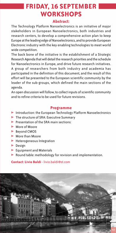
47
Abstract:The Technology Platform Nanoelectronics is an initiative of majorstakeholders in European Nanoelectronics, both industries andresearch centers, to develop a comprehensive action plan to keepEurope at the leading edge of Nanoelectronics, and to provide EuropeanElectronic industry with the key enabling technologies to meet worldwide competition.The back bone of the initiative is the establishment of a StrategicResearch Agenda that will detail the research priorities and the schedulefor Nanoelectronics in Europe, and drive future research initiatives.A group of researchers from both industry and academia hasparticipated in the definition of this document, and the result of thiseffort will be presented to the European scientific community by theleader of the sub-groups, which defined the main sections of theagenda.An open discussion will follow, to collect inputs of scientific communityand to refine criteria to be used for future revisions.
Programmet Introduction: the European Technology Platform Nanoelectronicst The structure of SRA: Executive Summaryt Presentation of the SRA main sections:t More of Mooret Beyond CMOSt More than Mooret Heterogeneous Integrationt Designt Equipment and Materialst Round table: methodology for revision and implementation.
Contact: Livio Baldi - [email protected]
FRIDAY, 16 SEPTEMBERWORKSHOPS

48
NOTES