prof. r. s. gamad
TRANSCRIPT

Prof. R. S. GAMAD
1. Personal Information
(i) Name Dr. R. S. Gamad
(ii) Qualification Ph. D.
(iii)
Designation Professor & Head
(iv) Email-id [email protected]/[email protected]
(v) Employee No.
3300293
(Vi) Department Electronics & Instrumentation Engineering
(vii) Experience 24 ear
2. Educational Qualification
No. Degree/Exam. Branch/ specialization Year of passing University/
Institute/
Board
1. 10+2/Higher
Secondary
Higher Maths 1991 M.P. Board, Bhopal
2. B.E.
Electronics Engineering 1995 Govt. Engineering
College Ujjain(M.P.) India
3. M.E.
Digital Techniques and
Instrumentation
2003 Shri G.S. Institute of
Technology and Science,
Indore//RGPV Technical
University, Bhopal
4. Ph.D.
E&I/ Testing of an A/D
Converter
2010 Shri G.S. Institute of
Technology and Science,
Indore /RGPV Technical
University, Bhopal

3. Research Interests
Analog & Mixed signal VLSI Design, ADC Design and Testing, Memory design, Wireless communication
4. Research Publications
(i) Book Chapter published:-
Dr. R. S. Gamad, chapter published in book “Advance in Electronics and
Communication Engineering” by AkiNik Publication,ISBN:978-93-90322-61-9,E-Book
ISBN:978-93-90322-62-6, in year 2020.
(II) Research Papers Published
(i) International Journal
S.No. Title of Research
Paper
Name of Journal and
Year/Issue No.
Publication as main
author or co-author
Remarks,
if any
Publications in 2009 as main author & Co-author
1. R. S. Gamad and D. K. Mishra, “Gain error, offset error and ENOB estimation of an A/D Converter using
histogram technique”, Published in Elsevier, International Journal of Measurement, Science direct
publication, Vol.42, No. 4, pp 570 – 576, May 2009. ISSN: 0263-2241. Impact Factor: 0.846.
2. R. S. Gamad and D. K. Mishra, “Determination of error in nonlinearity estimation in an A/D Converter with
triangular wave input”, Published in International Journal of Electronics, Taylor & Francis publications,
Vol. 96, No. 12, pp. 1237-1247, December 2009. ISSN: 0020-7217 Print/ISSN: 1362-3060 online. Impact
Factor: 1.257.
3. R. S. Gamad and D. K. Mishra, “Effects of Overdrive, Frequency, Sample and Error in Code Transition levels
on Computation on ENOB of an A/D Converter”, Published in International Journal of Electronics
Engineering Research ( IJEER), Research India publication, Vol. 1, No. 4, pp 3357 – 3365, 2009. ISSN:
0975-6450.
4. Namrata prasad, R. S. Gamad and C. B. Kushwah, "Design of a 2.2-4.0 GHz low phase noise and low power
LC VCO", Published in International Journal of Computer Network and Security (IJCNS), Malaysia,
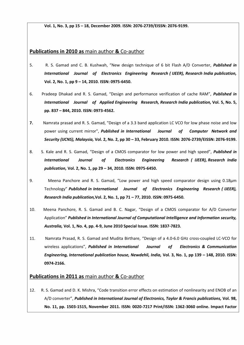
Vol. 1, No. 3, pp 15 – 18, December 2009. ISSN: 2076-2739/EISSN: 2076-9199.
Publications in 2010 as main author & Co-author
5. R. S. Gamad and C. B. Kushwah, “New design technique of 6 bit Flash A/D Converter, Published in
International Journal of Electronics Engineering Research ( IJEER), Research India publication,
Vol. 2, No. 1, pp 9 – 14, 2010. ISSN: 0975-6450.
6. Pradeep Dhakad and R. S. Gamad, “Design and performance verification of cache RAM”, Published in
International Journal of Applied Engineering Research, Research India publication, Vol. 5, No. 5,
pp. 837 – 844, 2010. ISSN: 0973-4562.
7. Namrata prasad and R. S. Gamad, "Design of a 3.3 band application LC VCO for low phase noise and low
power using current mirror", Published in International Journal of Computer Network and
Security (IJCNS), Malaysia, Vol. 2, No. 2, pp 30 – 33, February 2010. ISSN: 2076-2739/EISSN: 2076-9199.
8. S. Kale and R. S. Gamad, “Design of a CMOS comparator for low power and high speed”, Published in
International Journal of Electronics Engineering Research ( IJEER), Research India
publication, Vol. 2, No. 1, pp 29 – 34, 2010. ISSN: 0975-6450.
9. Meena Panchore and R. S. Gamad, “Low power and high speed comparator design using 0.18μm
Technology” Published in International Journal of Electronics Engineering Research ( IJEER),
Research India publication,Vol. 2, No. 1, pp 71 – 77, 2010. ISSN: 0975-6450.
10. Meena Panchore, R. S. Gamad and B. C. Nagar, “Design of a CMOS comparator for A/D Converter
Application” Published in International Journal of Computational Intelligence and Information security,
Australia, Vol. 1, No. 4, pp. 4-9, June 2010 Special Issue. ISSN: 1837-7823.
11. Namrata Prasad, R. S. Gamad and Mudita Birthare, “Design of a 4.0-6.0 GHz cross-coupled LC-VCO for
wireless applications”, Published in International Journal of Electronics & Communication
Engineering, International publication house, Newdehli, India, Vol. 3, No. 1, pp 139 – 148, 2010. ISSN:
0974-2166.
Publications in 2011 as main author & Co-author
12. R. S. Gamad and D. K. Mishra, “Code transition error effects on estimation of nonlinearity and ENOB of an
A/D converter”, Published in International Journal of Electronics, Taylor & Francis publications, Vol. 98,
No. 11, pp. 1503-1515, November 2011. ISSN: 0020-7217 Print/ISSN: 1362-3060 online. Impact Factor

1.257.
13. R. S. Gamad and N. Prasad, “layout design of LC VCO with current mirror using 0.18μm Technology”,
Published in International Journal of Wireless Engineering and Technology, Scientific Research
publishing, Inc., USA, Vol. 2, No. 2, pp. 102-106, April 2011, ISSN: 2152-2294.
14. R. S. Gamad and D. K. Mishra, “Computation of error in estimation of nonlinearity in ADC using Histogram
technique”, Published in International Journal of Engineering, Scientific Research publishing, Inc., USA,
Vol. 3, No. 6, pp. 583-587, June 2011, ISSN: 1947-3931.
15. Ankit Gupta and R. S. Gamad, “Design of a single stage source coupled CMOS VCO using 180 nm
Technology”, Published in International Journal of Engineering Research and Application, Vol. 1, No. 2,
pp. 122-124, July 2011. ISSN: 2248-9922.
16. Shubhara Yewale and R. S. Gamad, “ Analysis and design of a high gain low power fully differential gain
boosted folded-cascode op-amp with settling time optimization”, Published in International Journal of
Engineering Research and Application, Vol. 1, No. 3, pp. 666-670, 2011. ISSN: 2248-9922.
Publications in 2012 as main author & Co-author
17. Neha Bakawale, Manish Jain and R. S. Gamad “Design and performance verification of current conveyor
based pipeline A/D Converter using 180 nm Technology” Published in International Journal of
European Scientific Journal” Published by European Scientific Institute, PP 118-131, Vol. 8, No.27, Nov.
2012, ISSN: 1857-7881. Impact Factor 1.2875.
18. Shubhara Yewale and Radheshyam Gamad, “Design of low power and high speed CMOS comparator for
A/D converter application”, Published in International Journal of Wireless Engineering and Technology,
Scientific Research publishing, Inc., USA, Vol. 3, No. 3, pp. 90-95, April 2012. ISSN: 2152-2294.
19. Priyanka Dubey and R. S. Gamad, “Layout design of large bandwidth CMOS inverter based positive second
generation current conveyor”, Published in International Journal of Electronics Engineering
Research ( IJEER), Research India publication, Vol. 4, No. 2, pp 123 – 131, May 2012. ISSN: 0975-6450.
Publications in 2013 as main author & Co-author
20. Ajay shukla, R. S. Gamad and Rohan Raikwar, “Design of a CMOS optical Receiver front-end Using 0.18 µm
Technology” Published in International Journal of Wireless Engineering and Technology, Scientific
Research publisher, USA, PP 46-53, Vol. 4, January 2013. USA. ISSN: 2152-2294.
21. Rajani Gupta, P. Bansod and R. S. Gamad, “Quality Measure of the Compressed ECHO, X-Ray and CT
Images” Published in International Journal of Images and graphics, world scientific publishing

company, PP. 01-29, Vol. 13, No. 1, April 2013.
22. Vinod Kumar and R. S. Gamad, “ Design of a ring oscillator using CS-CMOS for mixed signal SOCs,”
Published in International Journal of Electrical and Electronics Engineering, PP. 21-26, Vol. 2, No. 2,
May 2013, ISSN 2278-9944 (Print), Impact Factor: 1.685
23. Vikas Kumar and R. S. Gamad, “ Design of a UHF band LNA using active inductor with FFP noise cancelling
technique”, Published in International Journal of Electronics and Communication Engineering &
Technology, PP. 124-131, Vol. 4, No. 3, May-June 2013, ISSN 0976-6464 (Print), Impact Factor: 5.8896
(by GISI).
24. Vaishali Naik, R. S. Gamad and P. P. Bansod, “Carotid Artery Segmentation in Ultrasound Images and
Measurement of Intima-Media Thickness,” Published in BioMed Research International Journal,
Hindawi publication, PP. 1-10, Vol. 2013, June 2013. Impact Factor: 2.880
25. Manish Jain and R. S. Gamad, “ Rlative techniques with Histogram technique for estimation of different
testing strategy of ADC,” Published in International Journal of Advanced research in computer science
and software Engineering,PP. 1379-1382, Vol. 3, No. 10, Oct. 2013, ISSN 2277-128X
2014-15
26. Dr. R.S. Gamad presented paper on “Design of a CMOS Optical Receiver Front end using 0.18µm
Technology”in Wireless Engg. And Technology(Scientific Research) 2013,Vol.4 Page No. 46-53.
27. Dr. R.S. Gamad presented paper on “Design and Performance Verification of Current Conveyor based
Pipeline ADC using 180nm Technology in Europeon Scientific Journal Nov.2013 Vol.8,ISSN:1857-7881.
28. Dr. R.S. Gamad presented paper on “Design of Ring Oscillator using CS-CMOS for Mixed Signal SoCs”in
IJEEE,Vol.2,Issue 2,May 2013,ISSN:2278-9944.
2015-16
29. Nivedita Jaiswal and Dr.R.S. Gamad Presented paper on “Design of a New Serializer and Deserializer
Architecture for OnchipSerDesTransceivers” in Circuits and systems,2015,6.
30. Ajay Agrawal and Dr.R.S. Gamad Presented paper on “Design of A Low power 1.65GBPS Data Channel for
HDMI Transmitter” in International Journal of VLSI Design and Communication system (VLSICS) Vol. 6
No. 6 ,Dec. 2015,DOI: 10.5121/vlsic.2015.6603.
2016-17
31. Alpana A. Deshmukh, Dr. R. S. Gamad and Dr. D. K. Mishra presented paper on “BIST Implementation
for Testing Analog Circuit in Mixed Signal Environment”in IJIRMF ,Vol. 2, Issue-10,ISSN:2455-0620, Oct-
2016.

32. Pushpendra Singh and Dr.R.S. Gamad presented paper on “A Bulk-Driven CMOS OTA with self -Biasing”
in IJESC 2016.Vol 6,Issue 9.
33. YudhishthirRaut, Dr. R.S. Gamad and Dr. P.P. Bansod presented paper on “Objective analysis of HEVC
(h.265) compressed FMRI Images”in IJCTA, 9(41), 2016, pp. 199-206, ISSN: 0974-5572.
34. AkhileshRajak and Dr. R.S. Gamad presented paper on “Design of a CMOS Differential difference
Amplifier” in JI of Instru. Soc of India, Vol. 46 Issue 2, june 2016.
2017-18
35. YudhishtirRaut,Dr. R. S. Gamadand Dr. P. P. Bansod presented paper on “Objective analysis and bit rate
analysis of HEVC compressed 4D-fMRI images” in International Journal of Imaging Systems and
Technology, DOI: 10.1002/ima.22315, March-2018.
36. Manish Sahajwani, Dr.Alok Jain and Dr.R.S. Gamad presented paper on “An Efficient Diversity
Achievement by Opportunistic Relaying in Amplify and Decode and Forward using ZF and MMSE
Equalizers” in IJDACR ,ISSN: 2319-4863, Vol:5 Issue 7 ,Feb. 2017.
37. Manish Sahajwani, Dr.Alok Jain and Dr.R.S. Gamad presented paper on “Performance Analysis of
Adaptive Modulation using Spatio Temporal Coding and Cooperative Communication ” in IJPAM .Vol114
Issue 9.2017,423-435,ISSN: 1311-8080.
2018-19
38. Shiv Ram Mansore, RadheshyamGamad and Dr. D. K. Mishra presented paper on “A single-ended
read disturb-free PPN based 9T SRAM cell”, Revue roumaine des sciences techniques
SerieElectrotechnique et Energetique, Vol. 63, No. 3,pp. 295-299,Dec. 2018. ISSN:0035-4066.
39. Alpana A. Deshmukh, Dr. R. S. Gamad and Dr. D. K. Mishra presented paper on “Modelling and
Simulation of Hilbert Transform Phase Detector Based on All Digital Phase Locked Loop” in
International Journal of Electronics Engineering, Volume 10 , Issue 2, ISSN: 0973-7383, pp. 648-664,
Dec-2018.
40. Alpana Amit Deshmukh, Dr.RadheshyamGamad and Dr.Deepak kumar Mishra presented paper on
“Implementation of Phase Locked Loop for FM Demodulator Circuit” in International Journal of
Engineering & Technology, Volume 7 (4) (2018), ISSN:6519-6522, doi: 10.14419/ijet.v7i4.28025, pp.
6519-6522.
41. Nidhi Khanna Renu Mehta and Dr. R. S. Gamad presented paper on “Low Power design of 4-bits
counter at circuit and system level of abstraction” in International Journal of Advanced Research,
Ideas and Innovations in Technology, Volume-4, Issue-5, ISSN:2454-132X, pp.249-251,Sep-2018.
42. ShivramMansore and Dr.RadheshyamGamad presented paper on “A data-aware write-assist 10T
SRAM cell with bit-interleaving capability” Turkish Journal of Electrical Engineering & Computer
Sciences, Vol.26,No. 5, sept.2018,ISSN:1300-0632.
43. S.R. Mansore, Dr. R. S. Gamad and Dr. D. K. Mishra presented paper on “Schmitt-Trigger Based
12T SRAM Cell with Enhanced Stability” in Journal of Semiconductor Devices and Circuits,
ISSN:2455-3379(Online), Volume 5, Issue 1,2018.
2019-20
44. S. R. Mansore, Dr. R.S. Gamad and Dr. D. K. Mishra presented paper on “A 32nm Read Disturb-

free 11T SRAM Cell with Improved write ability” in Journal of Circuits,Systems and Computers(world
scientific) ,Vol 29, Issue 05,ISSN:2050067, in 2020.
45. Mr. Virendra K. Verma, Dr. D. K. Mishra and Dr. R.S. Gamad presented paper on “Modelling and
Simulation of frequency Synthesizer based on Phase Locked Loop for RF Application” in Journal of
Engineering Services, Vol 11, Issue 02,ISSN:0377-9254,Feb-2020.
46. Pradeep Rajput, Mr. R. C. Gurjar and Dr. R. S. Gamad presented paper on “Low Phase Noise wide
Tuning Range LC Oscillator for RF Application using Varactor Bank” in Journal of
Telecommunication, Electronics and Computer Engineering (JTEC), Volume 11,Issue-3, ISSN:2180-
1843, E-ISSN:2289-8131, July-Sep. 2019.
47. Shubham Nigam, Dr. D. K. Mishra and Dr. R.S. Gamad presented paper on “Image Compression by
Wavelet Transform Using VHDL” in Journal of Applied Science and Computations (JASC), Volume VI,
Issue VI, JUNE/2019,ISSN NO:1076-5131, Page No:3060.
48. Mr. Virendra K. Verma, Dr. D. K. Mishra and Dr. R.S. Gamad presented paper on “Design of Low
Power Delay Cell for Wide Tuning Voltage Controlled Oscillator for Frequency Synthesis
Applications” in International Journal of Recent Technology and Engineering (IJRTE), Volume-7 Issue-
5, ISSN: 2277-3878,pp- 255-259,Jan-2019.
(ii) National Journal
Publications in 2003 as main author
49. R. S. Gamad, Mrs Anjana Jain and Mr. Shekhar Sharma, “Software implementation for error detecting
and correcting using Linear Block code in digital communication”, Published in Technical Journal,
Military College of Telecommunication Engineering, Mhow, India, pp. 109-121, January 2003.
Publications in 2007 as main author
50. R. S. Gamad and D. K. Mishra, “Estimation of variance for Gain and offset error of an ADC using
cumulative Histogram Technique”, Published in Engineering and Environmental Sciences Journal India,
Vol. 1, No. 3, pp 10-15, Jan.– June 2007. ISSN: 0972-9693.
Publications in 2010 as main author
51. R. S. Gamad and D. K. Mishra, “Comparative Evaluation of dynamic testing of A/D Converter using
Histogram Technique” Published in Research Journal of Institute of Engineers (IE)-ET, India, Vol. 90, pp.
17- 20, January 2010.
Publications in 2011 as main author
52. R. S. Gamad and N. Prasad, “Design of an LC VCO for low phase noise and low power consumption”,
Published in Research Journal of Institute of Engineers IE(I) Journal-EL, India, Vol. 91, pp. 18- 21,
March, 2011.

iii) International Conference
S. No. Title of Paper Name of Conference Place/Date
Organizing
Society/
Institute
Remarks,
if any
53. D. K. Mishra and R. S. Gamad, “ Dynamic Testing of and ADC for Real Application input” Published in IEEE AutoTestcon International Conference, Baltimore, MD, USA, September 12-15, 2011, PP. 354-359.
54. Balchand Nagar and R. S. Gamad, “Comparative Evaluation of Flash ADC Design” Published in International Conference on MEMS & Optoelectronics Technologies, Jan. 22-23, 2010, pp. 229- 234.
55. R. S. Gamad & D. K. Mishra, “Estimation of error in nonlinearity in ADC using standard histogram technique” International conf. on circuits and systems (WCECS), San Francisco, USA 22- 24 oct. 2008. pp-185-188.
56. R. S. Gamad & D. K. Mishra, “Determination of non linearity and effective resolution of an A/D converter for arbitrary Application input” International conf. on Circuits and systems, San Francisco USA 24-26 Oct. 2007. pp 220-223.
57. R. S. Gamad and D. K. Mishra, “Determination of Gain error & Offset error using Histogram Technique” International conf. on ICSCIS-07 J.E.C. Jabalpur, INDIA 27-29, Dec.2007, pp 186-191.
58. R. S. Gamad, D. K. Mishra and Sunny Gupta, ''Computation of Some A/D Converter Parameters Based on Error Estimation using Histogram Test Method'' International conf. SPIT-IEEE Colloquium 07, Mumbai, India, 4-5 Feb. Vol. 2 pp 183 - 189, 2008.
59. R.S. Gamad, D. K. Mishra and Sunny Gupta "Error Estimation in Code Transition Levels and in INL of an ADCs using Histogram Test Technique" international conf. on VLSI design and embedded system(ICVLSI- 08), pp 139 - 144,14 - 16 Feb. 2008, Chennai, India.
60. Manish Jain, Sunny Gupta & R. S. Gamad "FPGA based network on chip (NOC) implementation of scalable router" international conf. on VLSI design and embedded system(ICVLSI- 08), pp 209 - 212,14 - 16 Feb. 2008, Chennai, India.
61. Anand Sevda, Arun Sunaniya & R. S.Gamad “Design and optimization of noise, power consumption and slew rate of a two stage CMOS op amp" International Conf. on advances in computing (ICAC-08),

21-22 Feb. 2008, Chikhli, India.
62. R.S.Gamad & Mahendra Singh, A Switched Opamp with rail to rail common mode input range, International conf. (IEEE, RACE Bikaner 24-25 march 2007.
63. R.S. Gamad & K. Samadhiya, Advanced high Performance bus arbiter, International conf. (IEEE, RACE Bikaner 24-25 march 2007.
64. R.S.Gamad & Hemant Saxena, FIFO controller Design techniques in JPEG 2000 encoder, International Conf. on Modeling & Simulation Coimbatore, 27-29 August 2007.
65. R. S. Gamad & Hemant Saxena, Arbiter design Technique with first come first served priority scheme, National Conf. on VLSI and Comm. Engg.16-17 march 2007, pp. 35-37.
66. R. S. Gamad & K. Samadhiya, Advanced high Performance bus arbiter, 4th Level National Technical Symposium Feb. 2007 Bhopal.
67. R. S. Gamad & A. Sujalpurkar, Implementation of E-Primer data rate 2.048 Mbps Technology through VHDL Coding, National Conference on Information Technology (ITEEPP-07), April 06-07, 2007 Thapar University Patiala, India.
68. R. S. Gamad & M. Singh, A Switched Op-amp with rail to rail common mode input range, National Conference on Information Technology (ITEEPP-07), April 06-07, 2007 Thapar University Patiala, India.
69. Sunny Gupta, R.S.Gamad & Manish Jain " op-amp design for 12 bit ADC with fast settling time and higher bandwidth" National Conf. on challenges of power sector in 21st century, pp 122-125, 13-14 Nov. 2007, Jabalpur, India.
70. Sunny Gupta, A. Shujalpurkar & R.S.Gamad " Fault testing of telephone block modem through atrenta's spyglass tool " National Conf. on challenges of power sector in 21st century, pp 116-119, 13-14 Nov. 2007, Jabalpur, India.
71. Anand sevda, Arun sunaniya , R.S. Gamad & Manish Jain "Design & Optimization of Noise & Power Consumption of a Two-stage CMOS OP-AMP " National level conf. SGSITS, Indore, India, Page 402-406, 18-20 Dec. 2007.

5. List of Conferences/Workshops/STTP/FDP/Seminars Organized
S.No. Details of scientific EVENT Year Sponsored Agency
1. Recent Trends in VLSI Design( 5 day STC at SGSITS Indore) Apr-18 TEQIP-III
2. Advancement in Microelectronics and VLSI Design(5 days STTP at SGSITS Indore) March-19 TEQIP-III
3. VLSI Design and Test(International Symposiom, collobration with IIT Indore)
Jul-19 TEQIP-III, VLSI Society of India
4.
Design and development of system on Chip using Low power VLSI(6 days STTP at SGSITS Indore) Nov-19 AICTE
5.
Mixed Signal and Radio Frequency VLSI Design
Nov. 23 -28, 2020
AICTE
6.
Mixed Signal and Radio Frequency VLSI Design(3 STTPs online organized by E & I Engg. SGSITS Indore )
Dec. 07 – 12, 2020
AICTE
7.
Mixed Signal and Radio Frequency VLSI Design(3 STTPs online organized by E & I Engg. SGSITS Indore )
Dec. 14 – 19,
2020
AICTE
6. Invited Lectures/Expert Talks/Chairmanships at Conferences
1. Dr. R.S. Gamad Professor, delivered an online expert lecture on “Research
objective and challenges in Mixed Signal and RF VLSI Design” at AICTE
sponsored STTP (Short Term Training Program) on “ Mixed Signal and Radio
Frequency VLSI Design” on 23/11/2020, 7/12/2020 and 15/12/2020.
2. Dr. R.S. Gamad Professor, delivered an online expert lecture on "How to start
Research and Research Paper Writing" at B.M. Institute of Technology

and Science, Indore on 29th June 2020.
3. Dr. R.S. Gamad Professor, delivered an online expert lecture on "How to start
Research and Research Proposal Writing" at Mandsaur University, Indore on
15th September 2020.
4. Dr. R.S. Gamad Professor, delivered an expert lecture on "How to start
Research and Research Paper Writing" at B.M. Institute of Technology and
Science, Indore on 16th September 2017.
5. Dr. R.S. Gamad Professor, delivered an online expert lecture on "Importance
of ADC in Wireless Communication" at B.M. Institute of Technology and
Science, Indore on 17th February 2018.
10. Invited Lectures/Talks Delivered
(i) Expert Lecture on Data converter, 20/06/2009 at MIT, Ujjain.
(ii) Expert lecture on VLSI design, 17/07/2010 at MIT, Ujjain
(iii) Invited talk on testing techniques of ADC, National level techno-management
ELECTRIC 2011 at MIT, Mandsuar.
(iv) Expert lecture on Analog design and process modeling, 12/03/2011 at MIT, Ujjain.
(v) Session chair in National level conf. At Sanghavi Inst. 2012, Indore.
(vi) Expert lecture on VLSI design and testing, 20/10/2012 at MITS, Ujjain.
(vii) Session chair in National level conf. 19/12/2013 at Prestige Institute, Indore.
(viii) Session Chair in National level Conf. 15-16 march 2013 at SVCE, Indore.
(ix) Session chair in National level Techno- Management FEST, Chameli Devi. Institute,
Indore 12/03/2014.
(x) Expert lecture on DSP and its applications, 08/02/2014 at MIT Ujjain.
(xi) Keynote Speaker in National level Conf. on recent trends and issues in Engg. Tech.,
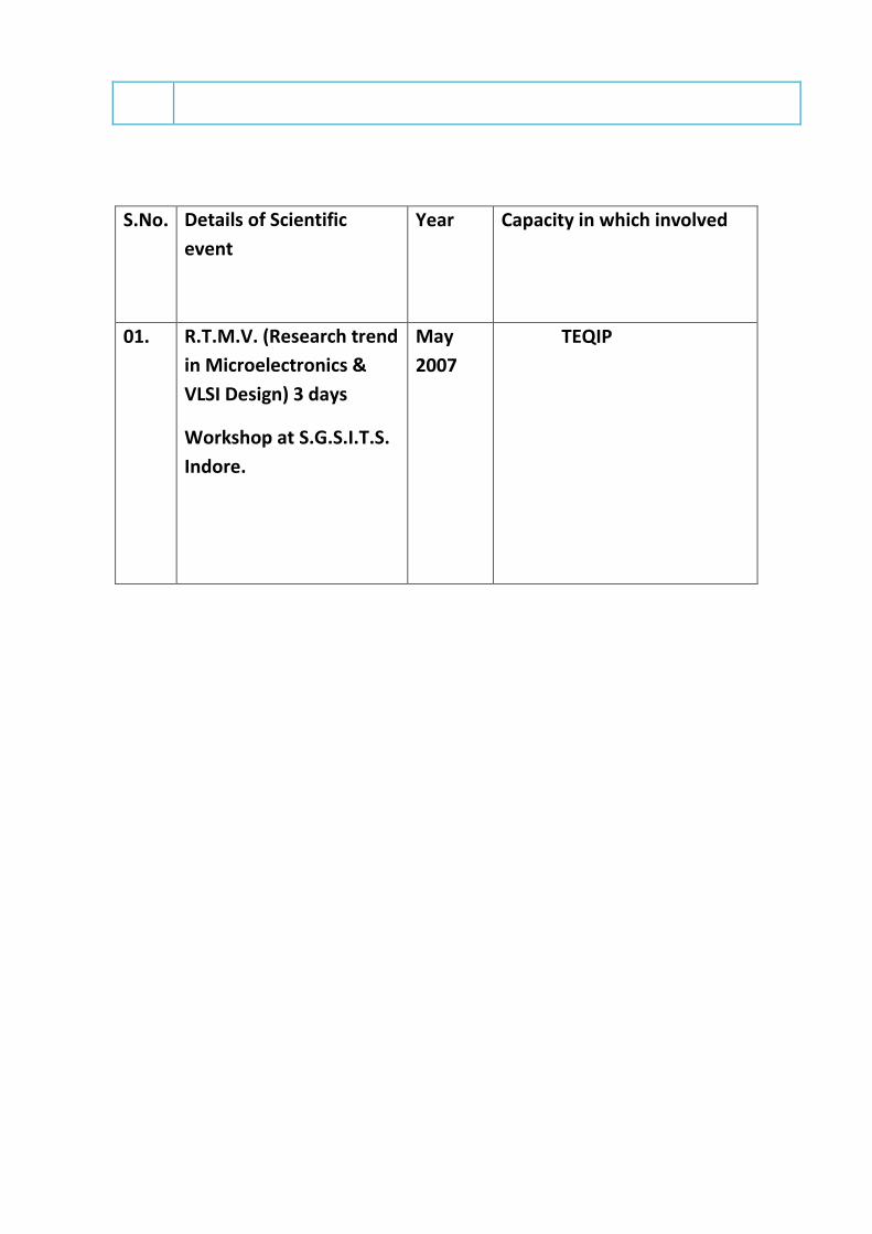
S.No. Details of Scientific
event
Year Capacity in which involved
01. R.T.M.V. (Research trend
in Microelectronics &
VLSI Design) 3 days
Workshop at S.G.S.I.T.S.
Indore.
May
2007
TEQIP