process improvement projects may 2006 dr. lynn fuller improvement projects 2006 ... solvent stripper...
TRANSCRIPT

© August 29, 2006 Dr. Lynn Fuller
Process Improvement Projects 2006
Page 1
Rochester Institute of TechnologyMicroelectronic Engineering
ROCHESTER INSTITUTE OF TECHNOLOGYMICROELECTRONIC ENGINEERING
Process Improvement Projects May 2006
Dr. Lynn Fuller Microelectronic Engineering
Rochester Institute of Technology 82 Lomb Memorial Drive Rochester, NY 14623-5604 Tel (585) 475-2035 Fax (585) 475-5041
Dr. Fuller’s Webpage: http://www.rit.edu/~lffeee Email: [email protected]
Dept Webpage: http://www.microe.rit.edu
8-29-2006 projects2006.ppt

© August 29, 2006 Dr. Lynn Fuller
Process Improvement Projects 2006
Page 2
Rochester Institute of TechnologyMicroelectronic Engineering
OUTLINE
Selective STI CMP Process Using Ceria SlurryResist Removal After Chlorine Plasma EtchTi Deposition in Perkin Elmer 2400Ti Deposition in CVC EvaporatorImproved SPCImproved CMOS TestingUse of Drytek Quad as Backup for Lam 490

© August 29, 2006 Dr. Lynn Fuller
Process Improvement Projects 2006
Page 3
Rochester Institute of TechnologyMicroelectronic Engineering
PROCESS IMPROVEMENT FOR STI CMP
Peng Xie and Mike Aquilino
Motivation: Past attempts at doing CMP for shallow trench (STI)using a generic oxide slurry (silica and high pH slurry) gave unsatisfactory results. Uniformity was especially poor. Wafer edge always over polished and wafer center was incomplete. The rate of removal of TEOS trench fill was low and the selectivity was low, ie. rate of polish of densified TEOS trench fill and rate of polish of nitride polish stop seemed to be equal.
A new slurry (Rodel Corp., CeO2, KOH, ph=10) made especially for STI was investigated. Excellent results were obtained and a new process was developed.

© August 29, 2006 Dr. Lynn Fuller
Process Improvement Projects 2006
Page 4
Rochester Institute of TechnologyMicroelectronic Engineering
PROCESS FLOW
§ Grow 500A Pad Oxide (thermal)§ Deposit 1500A Si3N4 by LPCVD
§ Level 1 Lithography to protect Active areas with photoresist
§ STI Trench Etch§ RIE in Drytek Quad§ Target: 4000A Si Trench
Peng Xie and Mike Aquilino

© August 29, 2006 Dr. Lynn Fuller
Process Improvement Projects 2006
Page 5
Rochester Institute of TechnologyMicroelectronic Engineering
PROCESS FLOW
§ Remove photoresist§ Grow 500A Liner Oxide (thermal)§ Repair damage to sidewalls
§ Deposit 6500A TEOS SiO2 by PECVD in Applied Materials P5000
§ CMP TEOS with Westech 372§ Nitride is stopping layer
Peng Xie and Mike Aquilino
© August 29, 2006 Dr. Lynn Fuller
Process Improvement Projects 2006
Page 6
Rochester Institute of TechnologyMicroelectronic Engineering
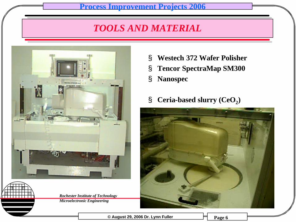
TOOLS AND MATERIAL
§ Westech 372 Wafer Polisher§ Tencor SpectraMap SM300§ Nanospec
§ Ceria-based slurry (CeO2)

© August 29, 2006 Dr. Lynn Fuller
Process Improvement Projects 2006
Page 7
Rochester Institute of TechnologyMicroelectronic Engineering
PROCESS VARIABLES (TOOL SETTINGS)
§ Slurry (Rodel Corp., CeO2, KOH, ph=10)§ Slurry flow rate (60 mL/min)§ Back pressure§ Carrier speed§ Platen Speed§ Down force§ Temperature (80°C)§ Polish time (2 min)§ Pad conditioning (1min per 4 wafers)
8100301.5470100
Down Force (PSI)
Platen Speed (RPM)
Carrier Speed (RPM)
Back Pressure (PSI)
P.S. Down Force/Wafer Pressure is controlled by gauge on side of tool. 80 PSI on gauge is 500 lbs of down force distributed over the area of 6” wafer (28.26 sq. in.) Thus Wafer Pressure = 0.2211 * Gauge Pressure
Peng Xie and Mike Aquilino
© August 29, 2006 Dr. Lynn Fuller
Process Improvement Projects 2006
Page 8
Rochester Institute of TechnologyMicroelectronic Engineering
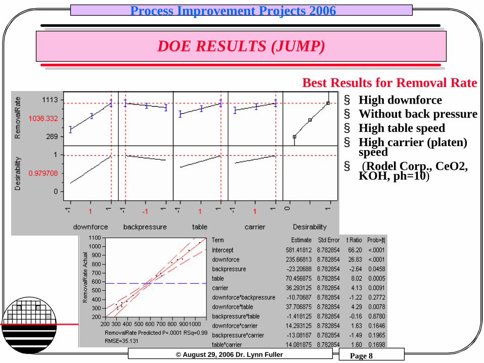
DOE RESULTS (JUMP)
§ High downforce§ Without back pressure§ High table speed§ High carrier (platen)
speed§ (Rodel Corp., CeO2,
KOH, ph=10)
Best Results for Removal Rate

© August 29, 2006 Dr. Lynn Fuller
Process Improvement Projects 2006
Page 9
Rochester Institute of TechnologyMicroelectronic Engineering
BLANK WAFER RESULTS USING BEST TOOL SETTINGS
§ Carrier speed: 30 RPM§ Platen speed: 100 RPM§ Without back pressure§ 8 PSI down force§ Slurry (Rodel Corp., CeO2, KOH, ph=10)§ Slurry flow rate (60 mL/min)
§ Oxide etch rate: 1040 A/min§ Nitride etch rate: 192 A/min§ Giving selectivity of 5.4:1§ Edge etches slower than the center!§ Poor uniformity (46%)
Tool Settings
Results
Peng Xie and Mike Aquilino

© August 29, 2006 Dr. Lynn Fuller
Process Improvement Projects 2006
Page 10
Rochester Institute of TechnologyMicroelectronic Engineering
ACTUAL FACTORY WAFER F050905
F050905 (oxide thickness = 6542 A)CMP for 2 min 30secSlurry (Rodel Corp., CeO2, KOH, ph=10)Slurry flow rate (60 mL/min)Clear all the dies except at the very edge two diesNitride etch rate: 170 A/minOxide etch rate: >3271 A/minSelectivity: >19:1Small dishing: 4493 A at 2 minObservation: Higher selectivity and etch rate observed on patterned
wafers (because effective down pressure is higher) CMP is highly pattern related!!!
Peng Xie and Mike Aquilino

© August 29, 2006 Dr. Lynn Fuller
Process Improvement Projects 2006
Page 11
Rochester Institute of TechnologyMicroelectronic Engineering
ACTUAL FACTORY WAFER F051010
F051010 (oxide thickness = 5286 A)CMP for 2 min 15secSlurry (Rodel Corp., CeO2, KOH, ph=10)Slurry flow rate (60 mL/min)Clear almost every die even at the edge Nitride etch rate: 170 A/minOxide etch rate: >2350 A/minSelectivity: >14:1Small dishing: 3800 A at 2 min 30secObservation: Higher selectivity and etch rate observed on patterned
wafers (because effective down pressure is higher) CMP is highly pattern related!!!
Peng Xie and Mike Aquilino
© August 29, 2006 Dr. Lynn Fuller
Process Improvement Projects 2006
Page 12
Rochester Institute of TechnologyMicroelectronic Engineering
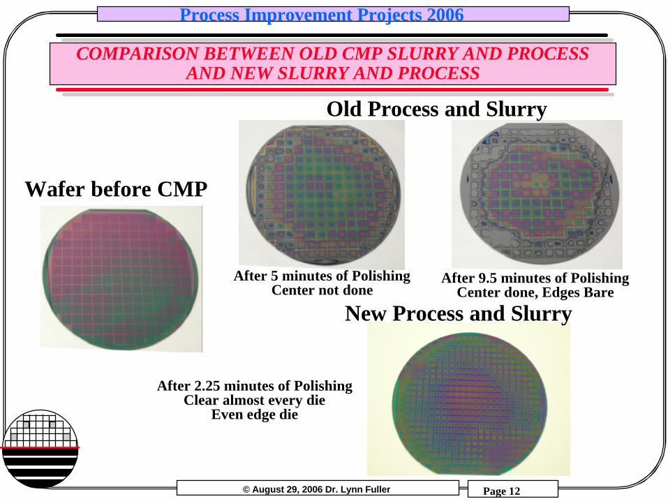
COMPARISON BETWEEN OLD CMP SLURRY AND PROCESS AND NEW SLURRY AND PROCESS
Wafer before CMP
Old Process and Slurry
After 9.5 minutes of PolishingCenter done, Edges Bare
After 5 minutes of PolishingCenter not done
After 2.25 minutes of PolishingClear almost every die
Even edge die
New Process and Slurry

© August 29, 2006 Dr. Lynn Fuller
Process Improvement Projects 2006
Page 13
Rochester Institute of TechnologyMicroelectronic Engineering
NEW FACTORY STI PROCESS (FACTSTI)
§ Carrier speed: 30 RPM§ Platen speed: 100 RPM§ Without back pressure§ 8 PSI down force (36 PSI on the gauge)§ Slurry (Rodel Corp., CeO2, KOH, ph=10)§ Slurry flow rate (60 mL/min)§ Pad conditioning: before every run§ Temperature: 80°C§ Polishing time: 2min 30 sec for 6500A oxide
Peng Xie and Mike Aquilino

© August 29, 2006 Dr. Lynn Fuller
Process Improvement Projects 2006
Page 14
Rochester Institute of TechnologyMicroelectronic Engineering
CMP SLURRY
Eminess Technologies, Inc.1620 West fountainhead Pkwy, Suite 510Tempe, AZ 85282Tel (408)505-3409, 888-899-1942, fax (480)951-3842
Darlene [email protected]
1/05/06 Order:N-2350-P Nalco 2350, 5 gal pail $166 each, Mfg by Rohm and Haas,
Silica, 70-100nm particle size, weight % 28, KOH, pH 11.4-12.4
R-10027556 Klebosol 1501-50 Colloidal Silica 5 gal pail $255 each, Mfg AZ Electronic Materials, Clariant’s Klebosol line of silica slurrys,50nm particles, KOH pH 10.9 50% solids
R-10087555 EXP CELEXIS CX94S Single Component Slurry, 20Liter pail $235 each, Mfg by Rohm and Haas Ceria 20nm particles, STI, pH ~7
http://www.EMINESS.comhttp://www.electronicmaterials.rohmhaas.com

© August 29, 2006 Dr. Lynn Fuller
Process Improvement Projects 2006
Page 15
Rochester Institute of TechnologyMicroelectronic Engineering
RESIST REMOVAL POST CHLORINE RIE ALUMINUM ETCH
Germain Fenger
Problem: Photoresist is hardened (and chemically changed) in Chlorine RIE during Aluminum etch and ashing is ineffective in removing the resist.
Solution: Use a Solvent based photoresist stripper process. (similar to Baselinc CMOS process at U of California at Berkeley)
Picture of aluminum wafers post chlorine RIE and after ashing. Note resist remaining on aluminum. Even very long ashing (60 min.) does not remove residue.

© August 29, 2006 Dr. Lynn Fuller
Process Improvement Projects 2006
Page 16
Rochester Institute of TechnologyMicroelectronic Engineering
MORE PICTURES OF RESIST SCUM PROBLEM
Pictures on left show resist residue after ashing. Pictures on right show effectiveness of ACT 935 solvent strip process.
From: [ACT-CMI Data Sheet]

© August 29, 2006 Dr. Lynn Fuller
Process Improvement Projects 2006
Page 17
Rochester Institute of TechnologyMicroelectronic Engineering
EXPERIMENT
Germain FengerDeposit TEOSDeposit AluminumMetal LithoMetal EtchResist Strip
ACT-CMI, 75C for 15 or 30 minor PRS2000, 90C for 30 min
Plasma Ash6” Factory Recipeor 6” Descum Recipe

© August 29, 2006 Dr. Lynn Fuller
Process Improvement Projects 2006
Page 18
Rochester Institute of TechnologyMicroelectronic Engineering
RESULTS FOR ACT CMI 75C for 15 or 30 min
Longer time did not make a difference
Germain Fenger

© August 29, 2006 Dr. Lynn Fuller
Process Improvement Projects 2006
Page 19
Rochester Institute of TechnologyMicroelectronic Engineering
RESULTS for Post Solvent Strip PLUS 6” Factory Plasma Ash
No photoresist was found on wafers
Germain Fenger

© August 29, 2006 Dr. Lynn Fuller
Process Improvement Projects 2006
Page 20
Rochester Institute of TechnologyMicroelectronic Engineering
RESULTS FOR PRS2000 90C for 30min
Much less photoresist on wafers then the ACT-CMI process
Germain Fenger
© August 29, 2006 Dr. Lynn Fuller
Process Improvement Projects 2006
Page 21
Rochester Institute of TechnologyMicroelectronic Engineering
RECOMMENDATIONS
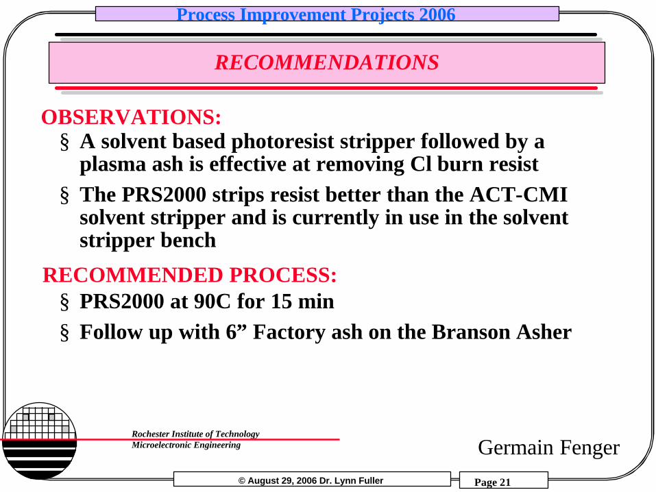
§ A solvent based photoresist stripper followed by a plasma ash is effective at removing Cl burn resist
§ The PRS2000 strips resist better than the ACT-CMI solvent stripper and is currently in use in the solvent stripper bench
§ PRS2000 at 90C for 15 min§ Follow up with 6” Factory ash on the Branson Asher
Germain Fenger
RECOMMENDED PROCESS:
OBSERVATIONS:

© August 29, 2006 Dr. Lynn Fuller
Process Improvement Projects 2006
Page 22
Rochester Institute of TechnologyMicroelectronic Engineering
Ti DEPOSITION USING P&E 2400B
ShrinivasShrinivas J J PandharpurePandharpure
OBJECTIVE
To develop a Ti Deposition process using Perkin Elmer 2400B sputtering tool (a factory backup process for CVC 601 tool)

© August 29, 2006 Dr. Lynn Fuller
Process Improvement Projects 2006
Page 23
Rochester Institute of TechnologyMicroelectronic Engineering
Ti DEPOSITION USING P&E 2400B
§ Sputtering Power: 500 W for 158 Å/min§ Base Pressure: < 5 x 10⁻⁶ Torr§ Sputtering Pressure: 8 mTorr (Argon flow:15 sccm)§ Deposition Time: 380 Seconds to get 1000Å Thickness§ Thickness standard deviation 4% (30 Å)§ Pre-Sputtering: 5 minutes same power
RESULTS
ShrinivasShrinivas J J PandharpurePandharpure

© August 29, 2006 Dr. Lynn Fuller
Process Improvement Projects 2006
Page 24
Rochester Institute of TechnologyMicroelectronic Engineering
Ti DEPOSITION USING CVC EVAPORATOR
Jirachai Getpreecharsawas
OBJECTIVETo develop a Ti Deposition process using CVC Evaporator
(a factory backup process for CVC 601 tool)
Current
Tungsten Basket
Ti Pellet
CVC 601
Waferf = m
4d π h2
f = film thicknessd = densityh = heightm = mass

© August 29, 2006 Dr. Lynn Fuller
Process Improvement Projects 2006
Page 25
Rochester Institute of TechnologyMicroelectronic Engineering
PHYSICAL PROPERTIES OF TI AND W
§ Titanium (Ti) : Melting point, Tmelt = 1675 °C
§ Tungsten (W): Melting point , Tmelt = 3410 °C
106710-8
123510-6
145310-4
Tvapor (°C)Vapor Pressure (Torr)1/8?
1/8?
Note: Ti sublimes since Tvapor < Tmelt
99.995% pure0.108 gram/pellet
Jirachai Getpreecharsawas

© August 29, 2006 Dr. Lynn Fuller
Process Improvement Projects 2006
Page 26
Rochester Institute of TechnologyMicroelectronic Engineering
Ti DEPOSITION USING CVC EVAPORATOR
Load wafer, 1 or 2 pellets of Ti in a tungsten boatPump ~60 min to reach base pressure <2E-6TStart deposition with shutter closed
(open after filament is hot)Evaporate at Variac setting of ~245Wait 5 min.Turn down Variac to zeroShut off filament power.Remove waferMeasure thickness on
Tencore alpha step 200
163.581366.6784.84340.001.6 × 10-6
138.48469.44176.16321.673.4 × 10-6
STDMean (Å)STDMean (Å)2 Pellets of Ti1 Pellet of TiPressure
(Torr)
Kapton TapeJirachai Getpreecharsawas
© August 29, 2006 Dr. Lynn Fuller
Process Improvement Projects 2006
Page 27
Rochester Institute of TechnologyMicroelectronic Engineering
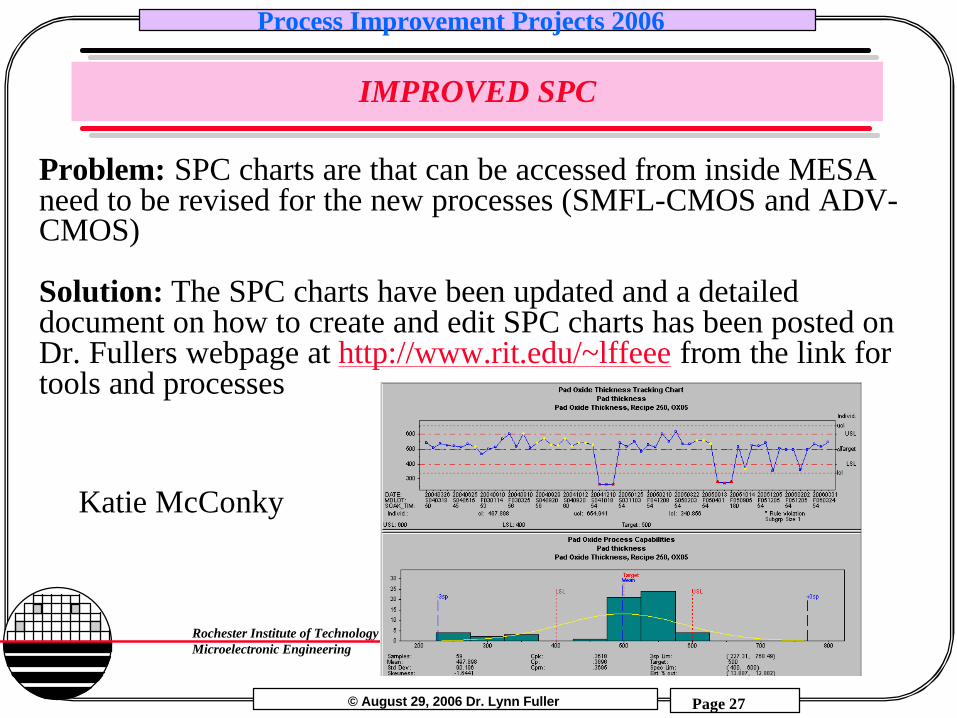
IMPROVED SPC
Problem: SPC charts are that can be accessed from inside MESA need to be revised for the new processes (SMFL-CMOS and ADV-CMOS)
Solution: The SPC charts have been updated and a detailed document on how to create and edit SPC charts has been posted onDr. Fullers webpage at http://www.rit.edu/~lffeee from the link for tools and processes
Katie McConky

© August 29, 2006 Dr. Lynn Fuller
Process Improvement Projects 2006
Page 28
Rochester Institute of TechnologyMicroelectronic Engineering
IMPROVED CMOS TESTING
Problem: Documentation for wafer testing of completed CMOS devices is inadequate.
Solution: A complete, very detailed, set of instructions have been developed for basic testing of CMOS wafers. This document is available on Dr. Fullers webpage at http://www.rit.edu/~lffeee from the link for tools and processes
David Pawlik

© August 29, 2006 Dr. Lynn Fuller
Process Improvement Projects 2006
Page 29
Rochester Institute of TechnologyMicroelectronic Engineering
USING THE DRYTEC QUAD AS A BACKUP FOR LAM 490
Problem: When the Lam490 is down wafers can be etched in the Drytech Quad however etch recipes giving similar etch rates and selectivity's need to be developed.
Drytech Quad

© August 29, 2006 Dr. Lynn Fuller
Process Improvement Projects 2006
Page 30
Rochester Institute of TechnologyMicroelectronic Engineering
USING THE DRYTEC QUAD AS A BACKUP FOR LAM 490
Solution: Recipes have been developed and have been published in a document (Quad_recipes.ppt). This document is available on Dr. Fullers webpage at http://www.rit.edu/~lffeee from the link for tools and processes