printed dipole antenna design for wireless...
TRANSCRIPT

Printed Dipole Antenna Design For Wireless Communications
Chun Yiu Chu
Department of Electrical & Computer Engineering McG ill University Montreal, Canada
July 2005
Design Techniques and Improvement on the Popular Printed Dipole Antenna.
© 2005 Chun Yiu Chu
2005/01/26

1+1 Library and Archives Canada
Bibliothèque et Archives Canada
Published Heritage Branch
Direction du Patrimoine de l'édition
395 Wellington Street Ottawa ON K1A ON4 Canada
395, rue Wellington Ottawa ON K1A ON4 Canada
NOTICE: The author has granted a nonexclusive license allowing Library and Archives Canada to reproduce, publish, archive, preserve, conserve, communicate to the public by telecommunication or on the Internet, loan, distribute and sell theses worldwide, for commercial or noncommercial purposes, in microform, paper, electronic and/or any other formats.
The author retains copyright ownership and moral rights in this thesis. Neither the thesis nor substantial extracts from it may be printed or otherwise reproduced without the author's permission.
ln compliance with the Canadian Privacy Act some supporting forms may have been removed from this thesis.
While these forms may be included in the document page cou nt, their removal does not represent any loss of content from the thesis.
• •• Canada
AVIS:
Your file Votre référence ISBN: 978-0-494-22639-1 Our file Notre référence ISBN: 978-0-494-22639-1
L'auteur a accordé une licence non exclusive permettant à la Bibliothèque et Archives Canada de reproduire, publier, archiver, sauvegarder, conserver, transmettre au public par télécommunication ou par l'Internet, prêter, distribuer et vendre des thèses partout dans le monde, à des fins commerciales ou autres, sur support microforme, papier, électronique et/ou autres formats.
L'auteur conserve la propriété du droit d'auteur et des droits moraux qui protège cette thèse. Ni la thèse ni des extraits substantiels de celle-ci ne doivent être imprimés ou autrement reproduits sans son autorisation.
Conformément à la loi canadienne sur la protection de la vie privée, quelques formulaires secondaires ont été enlevés de cette thèse.
Bien que ces formulaires aient inclus dans la pagination, il n'y aura aucun contenu manquant.

Abstract
With their planar structure and compatibility with the printed circuit fabrication tech
niques, printed dipole antennas present one of the best options for future wireless networks.
Although they have existed for a long time, printed dipole antennas are not vastly in use due
to their relatively large size. In this thesis, new design techniques are proposed to mini atur
ize these antennas. Other major improvements such as pattern correction and bandwidth
enhancement are also presented. The resulting antenna is then integrated with an IEEE
802.15.4 wireless transceiver on the same printed circuit board to show its functionality in
future wireless networks.

ii
Abrégé
Avec leur structure planaire et leur compatibilité avec les techniques de fabrication de
circuits imprimés, les antennes imprimées de dipôle offrent une des meilleures solutions pour
les futurs réseaux sans fil. Bien qu'elles existent depuis longtemps, les antennes imprimées
de dipôle ne sont pas énormément en service dû à leur relativement grande taille. Dans cette
thèse, on propose de nouvelles techniques de conception pour miniaturiser ces antennes.
D'autres améliorations principales telles que la correction de la diagramme de rayonnement
et l'augmentation de la bande passante sont également présentées. L'antenne modifiée est
alors intgrée avec un émetteur récepteur de protocoles IEEE 802.15.4 sur la même carte
électronique pour montrer sa fonction dans les futurs réseaux sans fil.

iii
Acknowledgments
If you asked me if l had thought about studying electrical engineering when l was a little
child, my answer would be NO. If you asked me if l had thought about studying electrical
engineering when l was a teenager (yes, l am too old to be called that now) , my answer
would still be NO. So, why am l doing what l am doing? It is a mystery for me. It still is.
It is also a miracle to me that l have gone this far. From my heart, l know that l could
not do it without the help of the following people. l owe them a lot and l am very grateful
for that.
First of aIl, l have to thank my supervisor Professor Milica Popovié for her insight and
valuable advice for the past two years. The whole journey would have been much more
difficult without her help. She is a great mentor and l enjoy very much being her student.
l also need to thank Professor Zeljko Zilié for his suggestions and new ideas on the papers
and the projects. He always shows me that there is space for improvement in anything. l
also want to thank him for allowing me to use the computer in the MACS lab (That Xilinx
machine really rocks!).
Sinee no soldier can fight alone, l have to thank my project partner and fellow comrade
Jean-Samuel Chenard for his help on everything. From measurements to test set-ups, his
enormous knowledge (1 am not exaggerating) on circuits and equipment (and anything
related to electrical engineering) continues to fascinate me. l learned much from him and
wish him aIl the best in the future.
l also need to thank Professor Ken Fraser and Professor Tho Le-N goc for letting me
do sorne of the measurements in the High Frequency Lab and the Telecommunications and
Signal Proeessing labo The paper will be not be complete without these data.

iv
Contents
1 Introduction 1
2 Momentum and HFSS: the differences between the two EM simulators 4
3 Preliminary designs 6
3.1 Broadband printed dipole antenna
with J-shaped integrated balun .. . . . . . . . . . . . . . . . . . . . . 6
3.1.1 Concept of the J-shaped bal un. . . . . . . . . . . . . . . . . . . 6
3.1.2 Simulation of the printed dipole with J-shaped integrated balun 10
3.2 Broadband printed dipole antenna
with via-hole integrated balun . . . . . . . . . . . . . . . . . . . . . . . 12
3.2.1 Concept of the via-hole balun . . . . . . . . . . . . . . . . . . . 12
3.2.2 Simulation of the printed dipole with via-hole integrated balun . 1:3
4 Miniaturization
4.1 Design concept for the miniaturized
"end-loaded" dipole antenna ....
16
16
4.2 Removal of the unnecessary ground plane. 17
4.3 Simulation of the miniaturized "end-loaded" dipole antenna 19
4.4 Comparison between the miniaturized "end-Ioaded" dipole antenna and the
preliminary design ............................... 19
5 Bandwidth Enhancement
5.1 Usage of tapered dipole arms
22
22
5.2 Combination of two techniques: Parasitic elements and Tapered dipole arms 25

Co~e~s v
5.2.1 Alternative design: Parasitic elements on opposite side of the tapered
arms ............... .
5.3 Summary of the results from aIl designs.
6 Pattern correction
6.1 Usage of bent dipole arms
6.2 Usage of asymmetrical coplanar strips .
6.2.1 Disadvantages of the asymmetrical coplanar strips .
7 Integration of antenna units within wireless networks
7.1 Requirements ................ .
7.1.1 Operating frequency and bandwidth
7.1.2 Impedance mat ching ........ .
7.1.3 Selection of the dielectric substrate material
7.2 Design methodology overview ........... .
7.2.1 Development of simplified model for fast simulation
7.2.2 Simulation results of the simplified model ... .
7.3 Effects of the PCB on the antenna performance ... .
7.3.1 Reduction of parallel-plate mode using via-holes
28
:31
32
32
33
34
38
38
39
~)9
39
40
41
42
4:3
45
7.3.2 Change in radiation patterns. . . . . . . . . . . 45
7.3.3 Comparison between the simplified model and the integrated antenna 47
7.4 Measurement and results
7.4.1 Return loss ...
7.4.2 Radiation patterns
8 Balanced antennas and microwave bal uns
8.1 Design of the balanced dipole antenna ..
8.1.1 Simulation setup and results ....
8.1.2 Disadvantage and alternative design.
8.2 Testing the balanced antenna ....... .
8.2.1 Design of the testing balun for the balanced antenna
47
47
49
50
50
51
53
56
56
8.2.2 Improved Marchand balun for testing . . . . . . . . . .58
8.2.3 Simulation results of the testing balun . . . . . . . . 60
8.2.4 Simulation results of the testing balun with the differential antenna 62

Contents -------------
8.3 Improving the balun performance at high frequency
8.3.1 Design configuration of the microwave balun
8.3.2 Simulation results for the microwave balun .
vi
64
66
67
8.4 Simulation results of the microwave balun with the unbalanced antenna 69
9 Conclusion 73
A Basic Thansmission Line Theory 75
A.1 Equations for the characteristic impedance of the microstrip line . . . . . 75
A.2 Theory behind the coupled Hne: Even-mode and Odd-mode propagation 75
References 78

List of Figures
3.1 Dipole antenna with a J-shaped integrated balun [1] printed on 0.OI7mm
thick Rogers R04350B substrate. The darker color indicates the top layer,
consisting of a microstrip line and the integrated J-shaped balun. The dipole
vii
structure is printed on the bottom layer. . . . . . . . . . . . . . . . . . .. 7
3.2 The integrated J-shaped balun is composed of a microstrip line, an open-
circuited stub, and coplanar strips. .................... 7
3.3 Coaxial-balun structure proposed in [2, 3]. Figure taken from [1]. ..... 8
3.4 Equivalent circuit of the coaxial-balun structure. Figure taken from [1]. 8
3.5 Simulated 811 for the broadband printed dipole antenna with J-shaped in-
tegrated balun of Figure 3.1. . . . . . . . . . . . . . . . . . . . . . . . . .. 11
3.6 Simulated E-plane and H-plane radiation patterns for the broadband printed
dipole antenna with J-shaped integrated balun of Figure 3.1. . . . . . . .. 11
3.7 Simulated cross-polarization level of the two printed dipole antennas (Figures
3.1 and 3.8) at 2.4GHz. . . . . . . . . . . . . . . . . . . . . . . . . . . . .. 12
3.8 Broadband dipole antenna with a via-hole integrated balun [4, 5] printed on
O.017mm-thick Rogers R04350B substrate. . . . . . . . . . . . . . . . . .. 13
3.9 Simulated 811 for the broadband printed dipole antenna with integrated via-
hole balun of Figure 3.8. . . . . . . . . . . . . . . . . . . . . . . . . . . .. 14
3.10 Simulated E-plane and H-plane radiation pattern for the broadband printed
dipole antenna with via-hole integrated balun of Figure 3.8. 15
4.1 Layout of the "end-Ioaded" miniaturized dipole antenna (modification of the
design of Figure 3.8). . . . . . . . . . . . . . . . . . . . . . . . . . . . . .. 18
4.2 Current distribution of the large printed dipole antenna with the integrated
via-hole balun shown in Figure 3.8. . . . . . . . . . . . . . . . . . . . . .. 18

List of viii
4.3 Simulated Sn for the miniaturized "end-loaded" printed dipole antenna of
Figure 4.1. . . . . . . . . . . . . . . . . . . . . . . . . . . . . . . . . . . .. 20
4.4 Simulated E-plane and H-plane radiation patterns for the miniaturized "end-
loaded" printed dipole antenna of Figure 4.1. . . . . . . . . . . . . . . . .. 20
4.5 Co/Cross polarization level for the miniaturized "end-loaded" printed dipole
antenna of Figure 4.1. ............................. 21
5.1 Layout for the "end-loaded" printed dipole antenna with tapered arms for
bandwidth enhancement. . . . . . . . . . . . . . . . . . . . . . . . . . . .. 23
5.2 Simulated Sn for the "end-loaded" printed dipole antenna with tapered arms
(Figure 5.1) for bandwidth enhancement. . . . . . . . . . . . . . . . . . .. 24
5.3 Simulated E-plane and H-plane radiation patterns for the "end-loaded" printed
dipole antenna with tapered arms of Figure 5.1. . . . . . . . . . . . . . .. 24
5.4 Co/Cross polarization level for the "end-loaded" printed dipole antenna with
tapered arms (Figure 5.1) for bandwidth enhancement. . . . . . . . . . .. 25
5.5 Layout for the "end-loaded" printed dipole antenna with tapered arms and
parasitic elements for bandwidth enhancement. ............... 26
5.6 Simulated Sn for the "end-loaded" printed dipole antenna of Figure 5.5 with
tapered arms and parasitic elements for bandwidth enhancement. ..... 27
5.7 Simulated E-plane and H-plane radiation patterns for the "end-loaded" printed
dipole antenna with tapered arms and parasitic elements of Figure 5.5. .. 27
5.8 Co/Cross polarization level for the "end-loaded" printed dipole antenna with
tapered arms and parasitic elements (Figure 5.5) for bandwidth enhancement. 28
5.9 Alternative design of Figure 5.5 with parasitic elements on opposite side of
the tapered arms. . . . . . . . . . . . . . . . . . . . . . . . . . . . . . . .. 29
5.10 Simulated Sn for the design of Figure 5.9 with parasitic elements on opposite
si de of the tapered arms. . . . . . . . . . . . . . . . . . . . . . . . . . . .. 29
5.11 Simulated E-plane and H-plane radiation patterns for the design of Figure
5.9 with parasitic elements on opposite side of the tapered arms. . . . . .. 30
5.12 Co/Cross polarization level for the design of Figure 5.9 with parasitic ele-
ments on opposite side of the tapered arms. ................. 30
6.1 Modified design of "end-loaded" dipole antenna of Figure 4.1 with arms
bending inward by 30 o. . . . . . . . . . . . . . . . . . . . . . . . . . . . .. 33

List of Figures ix
6.2 Null cancelation on the E-plane pattern due to the usage of 30 0 bent dipole
arms (Figure 6.1). . . . . . . . . . . . . . . . . . . . . . . . . . . . . . . .. ~34
6.3 Modified design of the antenna in Figure 6.1 with asymmetrical copI anar
strips and 20 0 bent arms . . . . . . . . . . . . . . . . . . . . . . . . . . .. 35
6.4 Current distribution of the antenna of Figure 6.3 with asymmetrical copI anar
strips. Strong current concentration on the 20 0 bent right arm cancels the
null at 90 0 on the E-plane. . . . . . . . . . . . . . . . . . . . . . . . . . .. :35
6.5 Simulated E-plane and H-plane radiation patterns for the "end-loaded" di-
pole antenna with asymmetrical coplanar strips and 20 0 bent arms for pat-
tern correction (Figure 6.3). . . . . . . . . . . . . .. . . . . . . . . . . .. 36
6.6 Simulated E-plane radiation pattern for the antenna with asymmetrical
coplanar strips (Figure 6.3) at different frequencies. The pattern is changing
with frequency. . . . . . . . . . . . . . . . . . . . . . . . . . . . . . . . " 37
7.1 Design flow of the integrated antenna. The full arrows show the order of the
design process. The dashed arrows designate the optional cycles that are
performed if there is significant mismatch between the lab results and the
simulation model. . . . . . . . . . . . . . . . . . . . . . . . . . . . . . . .. 42
7.2 Simplified model for fast simulation: Layout of the "end-loaded" miniatur-
ized dipole antenna with large ground plane that sums up the effect of nearby
objects on PCB (modification of the design in Figure 4.1). . . . . . . . .. 43
7.3 Simulated 8 11 for the simplified model with large PCB ground plane of Figure
7.2. Measurement of the real antenna is also shown for comparison. . . .. 44
7.4 Simulated E-plane and H-plane radiation patterns for for the simplified
model with large PCB ground plane of Figure 7.2. . . . . . 44
7.5 Complete PCB model with the integrated dipole antenna.
7.6 Return loss (811 ) of the integrated antenna of Figure 7.5 ..
7.7 Normalized E-plane and H-plane radiation patterns for the integrated an-
tenna of Figure 7.5 ............. .
46
48
48 7.8 The radiation pattern measurement setup. . . . . . . . . . . . . . . . . .. 49
8.1 Balanced dipole antenna based on the center-fed thin-wire dipole antenna. 52
8.2 The simulated return loss (811 ) of the balanced dipole antenna of Figure 8.1. 53

List of Figures x
8.3 Simulated E-plane and H-plane radiation patterns for the balanced dipole
antenna of Figure 8.1. 54
8.4 Miniaturized "end-loaded" balanced dipole antenna (modification of the de-
sign of Figure 8.1). . . . . . . . . . . . . . . . . . . . . . . . . . . . . . .. .54
8.5 The simulated return loss (S11) of the "end-loaded" balanced dipole antenna
of Figure 8.4. The results of the original antenna (Figure 8.1) with longer
arms are also shown for comparison. ..................... 55
8.6 Simulated E-plane and H-plane radiation patterns for the "end-loaded" bal-
anced dipole antenna of Figure 8.4. . . . . . . . . . . . . . . . . . . . . .. 55
8.7 Coaxial configuration of the Marchand balun and its equivalent planar struc-
ture (Figure taken from [6]). . . . . . . . . . . . . . . . . . . . . . . . . .. 57
8.8 Improved Marchand balun using tuning septum made by the reverse U-
shaped ground plane and an additional metal plate. . . . . . . . . . . . .. 60
8.9 Simulated return loss (S11 and S22) for the Marchand balun of Figure 8.8.. 61
8.10 Simulated insertion loss (S12 and S2d for the Marchand balun of Figure 8.8. 6~j
8.11 "End-loaded" differential dipole antenna of Figure 8.4 is attached to the
balun of Figure 8.8 before testing. . . . . . . . . . . . . . . . . . . . . . .. 64
8.12 Simulated return loss (S11) of the 'end-loaded" balanced dipole antenna with
the balun of Figure 8.11. . . . . . . . . . . . . . . . . . . . . . . . . . . .. 65
8.13 Simulated E-plane and H-plane radiation patterns for the "end-loaded" bal
anced dipole antenna with the testing balun (Figure 8.11). Patterns for the
same antenna without balun (Figure 8.4) are also shown for comparison .. 65
8.14 Layout of the microwave balun based on the folded Marchand balun. ... 66
8.15 Simulated return loss (S11 and S22) for the microwave balun of Figure 8.14. 68
8.16 Simulated insertion loss (S12 and S21) for the microwave balun of Figure 8.14. 68
8.17 Layout of the unbalanced "end-loaded" dipole antenna with the microwave
balun. . . . . . . . . . . . . . . . . . . . . . . . . . . . . . . . . . . . . .. 70
8.18 Simulated return loss (S11) of the unbalanced "end-loaded" dipole antenna
with the microwave balun of Figure 8.17. . . . . . . . . . . . . . . . . . .. 70
8.19 Simulated E-plane and H-plane radiation patterns for the unbalanced "end-
loaded" dipole antenna with the microwave balun of Figure 8.17. . . . . .. 71

List of Figures
A.l The coupled-line model and its equivalent capacitive network. C11 and C22
are the capacitance between each line and the ground. C12 is the mutual
xi
capacitance between the two lines (Figure taken from [7]). ......... 77
A.2 Even-mode excitation on a coupled line and its resulting equivalent capaci-
tance networks (Figure taken from [7]). . . . . . . . . . . . . . . . . . . .. 77
A.3 Odd-mode excitation on a coupled line and its resulting equivalent capaci-
tance networks (Figure taken from [7]). . . . . . . . . . . . . . . . . . . .. 77

xii
List of Tables
3.1 Summary of the antenna performance of the printed dipole antennas. . .. 15
4.1 Parameters used to control the resonant frequency of the antenna shown in
Figure 4.1. . . . . . . . . . . . . . . . . . . . . . . . . . . . . . . . . . . .. 17
4.2 Comparison between the miniaturized "end-Ioaded" dipole antenna (Figure
4.1) and its larger version (Figure 3.8). . . . . . . . . . . . . . . . . . . .. 21
5.1 Results of the antennas using different bandwidth enhancement techniques 31
6.1 Results of the antennas with different bending angles . . . . . . . . . . .. 33
6.2 Results of the antenna with asymmetrical coplanar strips and 20 0 bent arms
(Figure 6.3). . . . . . . . . . . . . . . . . . . . . . . . . . . . . . . . . . .. 36
7.1 PCB materials electric properties 40
8.1 Effects of the balun on the antenna performance of the "end-loaded" bal-
anced dipole antenna. . . . . . . . . . . . . . . . . . . . . . . . . . . . . .. 63
8.2 Comparison between the "end-loaded" dipole antenna (Figure 4.1) and the
same antenna with the microwave balun (Figure 8.17). ........... 71

1
Chapter 1
Introduction
Future wireless devices will require integration of antenna units with the rest of electronics
to reduce size and manufacturing cost. Among different types of antennas, printed antennas
are the ideal candidates for these applications due to their planar structure and compatibil
ity with the printed circuit fabrication techniques [8]. Printed antennas have diverse design
configurations, the most common ones are microstrip patch antennas [9], printed dipole
antennas [1], printed monopole antennas and their variants (e.g. the inverted-F) [10, 11].
Microstrip patch antennas might be the most popular printed antennas because of
their "low-profile, low-weight, low-cost, easy integrability into arrays or with microwave
integrated circuits, or polarization diversity" [9]. The major disadvantage is their narrow
bandwidth, which prevents their use in many applications. Extensive studies have been
do ne to solve this problem. Solutions include usage of parasitic elements [12], aperture
coupling [13], stacked patch configuration [14], etc.
Similar to the traditional monopole antennas, printed monopole antennas (including the
printed inverted-F and the printed inverted-L antennas) are fed against a ground plane. Ac
cording to the principles of Image Theory, the monopole and its image on the ground plane
will form a dipole antenna [8]. The printed monopole antennas are flexible for impedance
matching and can achieve moderate to wide bandwidth (300MHz to 1GHz) [10, 11], there
fore, they have recently been widely adopted in wireless communication systems. However,
since the antennas are installed on a finite ground plane, its size and shape can affect the
performance of the antennas [15].
Printed dipole antennas are the main foeus of this thesis. These antennas are ehosen
2005/07/26

1 Introduction 2
because they are simple and yet have potential for future improvement. Unlike the straight
wire di pole antennas, the radiating elements (i.e. the dipole arms) of the printed dipole
antennas are on a dielectric substrate. Therefore, the selection of the substrate material will
affect the performance of the antennas. It nevertheless makes the design of the antennas
more flexible. The major disadvantage of the printed dipole antennas is their relatively
large size. This is a major problem especially for applications at low frequency (less than
IGHz). However, as the operating frequency increases beyond the low-GHz range, this
problem will no longer prevail.
Most existing printed dipole antennas are based on the popular printed dipole design
first proposed in [1] in 1987. Unlike the traditional dipole antennas, this printed dipole
antenna has an integrated balun and can be fed by a 50-[2 single-ended microstrip line.
A voiding differential input facilitates the testing pro cess because most vector network an
alyzers (VNA) only have single-ended ports that cannot directly measure differential pa
rameters [16]. The characteristics of this antenna are studied in Chapter 3. In later work,
the same design was modified by replacing the quarter-wave open-circuited stub with a
via-hole balun [4, 5]. In this way, the bandwidth is increased; the undesired radiation and
coupling from the stub will be canceled out. The printed dipole antenna designs proposed
in this thesis are aIl based on this modified design. Major improvement techniques, includ
ing miniaturization, bandwidth enhancement, and pattern correction, have been studied
and presented in Chapter 4, Chapter 5, and Chapter 6, respectively.
AlI antenna designs presented here are simulated using two Electromagnetic (EM) sim
ulators. Momentum is a 2.5-D simulator based on Method of Moments (MoM) [17]. It is
ideal for printed antenna design but it does not support full-wave 3-D simulation. HFSS
is based on the finite-element method (FEM). It can solve 3-D electromagnetic problems
at the expense of higher cost in computation time and resources. To facilitate the design
process, Momentum is employed in the first stage of design. Then, HFSS is used to validate
the performance of the designs. The difference between the two simulators will be discussed
in Chapter 2.
Successful designs are fabricated and tested ta show the difference between simulation
models and fabricated real products. To examine the functionality of the proposed antenna
designs in wireless networks, one of them is integrated with an IEEE 802.15.4 (Zigbee)
wireless transceiver on a single printed circuit board (PCB). The Zigbee system is chosen
because it provides low-power wireless communications using the unlicensed 2.4-GHz band.

1 Introduction 3
The design methodology and analysis of the integration will be discussed in Chapter 7.
Since any additional device (including the balun network) introduces losses into the
system, it is worthwhile to study a complete differential RF front-end with a balanced
antenna. In Chapter 8, the design of a balanced dipole antenna is presented. The difficulties
of the differential measurement are also discussed. Finally, a new microwave balun is
proposed to improve the antenna performance in the higher frequency range.
The major challenge of this thesis is to design a printed dipole that is compact enough for
wireless applications without compromising the good characteristics (e.g. wide bandwidth,
omnidirectional radiation pattern, simple configuration, etc) of the traditional large-sized
dipole antennas. Thus, it is necessary to research new design techniques and configurations
to tackle this problem. Generally, different applications will have diverse requirements for
antennas. It is shown in this thesis that a few simple design techniques can make the
same printed dipole antenna satisfy different requirements. In addition, this thesis tries to
fill the gap between traditional circuit design and antenna design by showing a detailed
methodology for the integration of a dipole antenna within a wireless transceiver unit. The
me rit of the proposed methodology is that it is applicable to other antenna families. The
ultimate goal of this thesis is to serve as a starting point for anyone who is interested in
further exploring wireless antenna design.

4
Chapter 2
Momentum and HFSS: the
differences between the two EM
simulators
AIl antenna designs in this thesis are simulated using the following electromagnetic (EM)
simulators:
1. Momentum (Agilent Advanced Design System 2003A, [17]);
2. HFSS v.9.2.1 (Ansoft Corporation, [18]).
The main difference between the two simulators is how they calculate the effects of the
substrate layer. In the 2.5-D simulator Momentum, the dielectric substrate is extended
to infinity in space [17]. Infinite substrate simplifies the calculation and allows the reuse
of the substrate data, resulting in a much shorter simulation time. However, any abrupt
transition from substrate to air in the real antennas will be ignored. Therefore, any surface
wave bounced back from the edges will not be considered, thus introducing errors in the
calculation of the resonant frequency [19, 20]. Even though a waveguide or a box can be
used to set a finite-size substrate in Momentum, it is not applicable in the printed dipole
design because the antenna is not surrounded by metal sidewalls. The infinite substrate
layer also forbids simulation of the nearby components in the near-field. Another limitation
of the infinite substrate is the incorrect modeling of the radiation pattern in the far field
along the dielectric plane.
2005/07/26

2 Momentum and HFSS: the differences between the two EM simulators 5
In contrast, in the 3-D simulator HFSS, users can set both thickness and dimension
of the substrate. Thus, the effects of the surface wave bounced back from the edges are
considered within the simulation. This implies a doser match between the simulations and
measurement. Field strength measured along the dielectric plane on the fabricated antenna
was eventually found to dosely match the results of the 3-D HFSS simulations.
The accuracy of the HFSS tool is increased with respect to the accuracy level of Mo
mentum at the cost in computation time and resources. A typical simulation can last more
than 20 minutes on average. To reduce the simulation time, the conductive structure (such
as the microstrip li ne and the ground plane) could be drawn as a perfectly conducting
plane. This approach will reduce the simulation time, but also the accuracy level of the
obtained results. Since the conducting material has no thickness and infinite conductivity,
the metal effects will be ignored. Generally, the effect of the thin metal is not significant
at low to mid frequencies « IGHz). At higher frequency (or with a thick metal), the skin
effect starts to emerge and this approach is no longer applicable.
Due to these limitations, Momentum is ideal only in the early stage of the project. Once
a successful model is designed and tested in Momentum, more rigorous simulation using
HFSS is needed to validate its performance.

6
Chapter 3
Preliminary designs
Most existing printed dipole antennas are based on the popular printed dipole design first
proposed in [1] in 1987. For completeness, we first study the characteristic of this antenna
design.
3.1 Broadband printed dipole antenna
with J-shaped integrated balun
The antenna has a simple structure and has an integrated balun that allows the use of a
50-0 single-ended microstrip feed line. It is built on two metallic strip layers on opposite
sides of a dielectric substrate. The microstrip feed Hne, with the integrated J-shaped balun,
is on the top strip layer, whereas the dipole structure is printed on the bottom strip layer
(Figure 3.1).
3.1.1 Concept of the J-shaped balun
The integrated J-shaped balun is composed of 3 parts (Figure 3.2):
1. Quarter-wave microstrip line with characteristic impedance Zao
2. Quarter-wave open-circuited stub formed by a transmission line with characteristic
impedance Zb'
3. Quarter-wave short-circuited stub formed by coplanar strips (i.e. balanced line) with
characteristic impedance Zab'
2005/07/26

3 Preliminary designs
, 23 !iHll "'"~~~~,,~--------'""-'''~,;;' r----------------------,
Bottom
Top
.T- ml<ll) ell \);a!Ull
ltln,
Fig. 3.1 Dipole antenna with a J-shaped integrated balun [1] printed on O.OI7mm-thick Rogers R04350B substrate. The darker color indicates the top layer, consisting of a micros trip line and the integrated J-shaped balun. The dipole structure is printed on the bottom layer.
+ +
1 Copl:mol' stl'i)Js
ot.tll-ril'nlit." slll11
Fig. 3.2 The integrated J-shaped balun is composed of a microstrip line, an open-circuited stub, and coplanar strips.
7
3 Preliminary designs 8
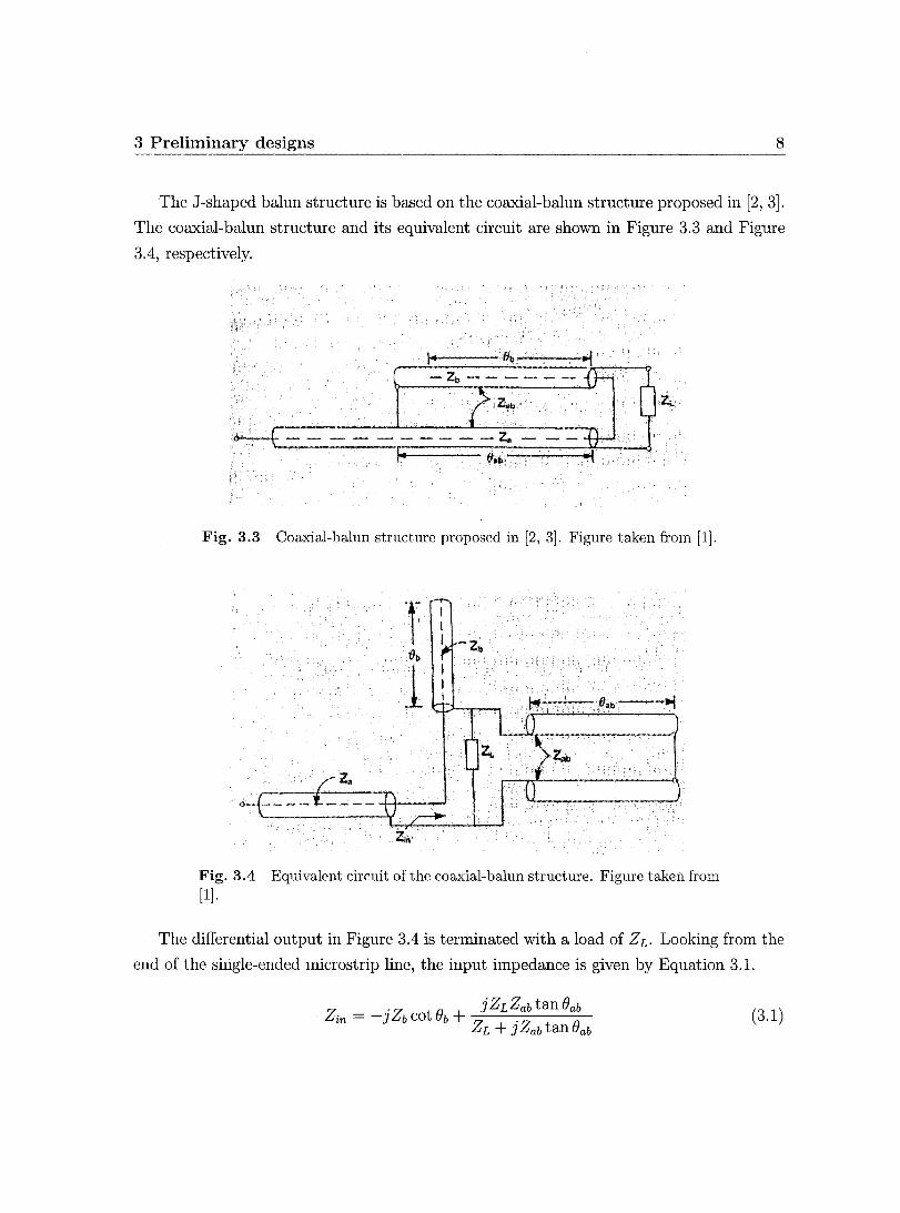
The J-shaped balun structure is based on the coaxial-balun structure proposed in [2, 3].
The coaxial-balun structure and its equivalent circuit are shown in Figure 3.3 and Figure
3.4, respectively.
- Zt, - - - - - -.
--+----------Za (J""
Fig. 3.3 Coaxial-balun structure proposed in [2, 3]. Figure taken from [1].
Fig. 3.4 Equivalent circuit of t.he coaxial-balun structure. Figure taken from [1].
The differential output in Figure 3.4 is terminated with a load of ZL' Looking from the
end of the single-ended microstrip line, the input impedance is given by Equation 3.1.
(3.1)

3 Preliminary designs 9
The first term in Equation 3.1 is the impedance of the open-circuited stub. The second
term is the impedance of the short-circuited stub in parallel with the load ZL. Notice
that the input impedance Zin will be simplified to ZL if the lengths of the stubs are both
equal to quarter-wavelength (i.e. eab = eb = 90°). When the balun is integrated with the
printed dipole antenna, the load ZL is equal to the input impedance of the dipole antenna.
The latter can be accurately determined by using a simple dipole model in EM simulators.
To facilitate the testing process, the microstrip line is used as a quarter-wave impedance
transformer, which matches the input impedance of the antenna (Zin) to the 50-0 port of
the VNA. The characteristic impedance Za of the microstrip line is determined as:
(3.2)
From this characteristic impedance, the dimension of the the microstrip line can be
determined using the equations given in the Appendix. Many GAD tools also use the
noted equations to calculate characteristic impedance of a microstrip line. The program
LineGal from the Agilent Advanced Design System (ADS) software package [17] is one
of them and is used for this calculation. Note that the equations in the Appendix are
applicable only if the width of the ground plane is at least three times wider than the
microstrip line [1]. Therefore, the width of the coplanar strips under the microstrip line is
set by this rule because the coplanar strips are served as the ground plane for the microstrip
line. Following this rule will simplify the design pro cess , but it is not mandat ory because
in certain cases, the width of the copI anar strips is no longer three times wider than the
micros trip line after optimization using the EM simulators.
Besides the width of the transmission lines in the balun, the lengths of the stubs can
be modified to improve the bandwidth of the balun. For example, the lengths eab and eb
deviate slightly from quarter-wavelength to widen the bandwidth [1]. Same result can be
achieved by designing the copI anar strips with a characteristic impedance Zab much higher
than the load impedance ZL. In that case, the second term in Equation 3.1 will be simplified
to ZL, independent of the length of the coplanar strips (Bab). Notice that the characteristic
impedance of the copI anar strips is dependent on the width of the lines, the space between
the lines, and the dielectric constant and thickness of the substrate material. Using GAD
tools to optimize these parameters, the bandwidth of the resulting antenna with an VSWR
of 2 or lower can be more than 40% [1].

3 Preliminary designs 10
3.1.2 Simulation of the printed dipole with J-shaped integrated balun
The design in Figure 3.1 is simulated using the 2.5-D simulator Momentum and validated
using the 3-D simulator HFSS. The antenna layout was drawn on two 0.017mm-thick copper
strip layers in between a dielectric substrate of Rogers HF material R04350B. The latter
has a thickness of 0.762mm, a dielectric constant (cr) of 3.48 and a loss tangent of 0.003l.
As mentioned previously, the dipole arm length, the microstrip feed line, and the open
circuited stub are aIl approximately quarter-wavelength long at the resonant frequency
(in this thesis, the chosen frequency is 2.4GHz). The exact dimension is then optimized
using both simulators. The antenna layout is best tested in Momentum in range 1-3 GHz,
resolving the short est effective wavelength of the model with at least 30 cells of the numerical
model mesh. The same antenna is then re-simulated using HFSS. To increase the solution's
precision, an adaptive analysis is applied in HFSS to refine the mesh iteratively in regions
where the error is high [18]. The iterative pro cess repeats until the convergence criteria set
by the user is met or the requested number of refinement cycles is completed. In HFSS, the
convergence criteria is the maximum relative change in the magnitude of the S-parameters
from consecutive passes (also known as maximum Delta S in HFSS). The antenna is best
tested in range 1-3 GHz with 3 mesh refinement cycles. The maximum relative change
between the S-parameters generated from consecutive passes is set to be less than 0.0l.
The simulation results are given from Figure 3.5 to Figure 3.7. The broadband char
acteristic of the antenna is shown in Figure 3.5. The results from HFSS show a return
loss (S11) less than -10dB from 2.2GHz to 2.9GHz, resulting in a bandwidth of 700MHz.
The bandwidth given by Momentum is slightly less than that obtained by HFSS, since
Momentum ignores surface wave bounced back from the edges of the substrate.
The patterns from both simulators practicaIlY overlap, therefore, only the HFSS results
are shown in Figures 3.6 and 3.7. The antenna has a gain of 2.86dB and efficiency of 85%.
The far-field radiation patterns resemble the ones of the typical half-wave dipole antennas,
which are omnidirectional on the H-plane (Figure 3.6). Since the dipole antenna is linearly
polarized, the cross-polarization level should be low. The simulated cross-polarization level
is less then -16.39dB on the H-plane at 2.4GHz (Figure 3.7).

3 Preliminary designs
-5
-10
00 ;- -15
en
-20
-25
_30L---~----~----L----L----~--~~---L----~--~~--~ 1 1.2 1.4 1.6 1.8 2 2.2 2.4 2.6 2.8 3
Frequency (GHz)
Fig. 3.5 Simulated Su for the broadband printed dipole antenna with Jshaped integrated balun of Figure 3.1.
s
330 30
270 f-+-I--Ic---8l*~E-t-+f+-I--+- 90 270 1--I--f--I--I----l-...:::;?oII,::...--I---l---+--l---1-
210 150
180 180
Fig. 3.6 Sirnulated E-plane and H-plane radiation patterns for the broadband printecl dipole antenna with J-shaped integrated balun of Figure 3.1.
Il
90

3 Preliminary designs
-10
-20 iil ~ c o
~ -25 co ë5 c.
~ u
-30
-35
_40L-____ J_ ____ -L ____ ~ ______ L_ ____ J_ ____ _L ____ ~_
o 150 200 250 300 350 Thela (deg)
Fig. 3.7 Simulated cross-polarization level of the two printed dipole antennas (Figures 3.1 and 3.8) at 2.4GHz.
3.2 Broadband printed dipole antenna
with via-hole integrated balun
12
A modified version of the broadband printed dipole antenna of Figure 3.1 was proposed in
2001 by replacing the quarter-wave open-circuited stub in the J-shaped balun with a via
hole balun [4, 5J (Figure 3.8). Avoiding the open-circuited stub can increase the bandwidth
of the antenna [5J. Most importantly, undesired radiation, coupling effect, and power los ses
from the stub will be canceled out [4J. AlI designs proposed in this thesis will be based
on this antenna with a via-hole balun. Rence, we outline the basic functioning of this
configuration.
3.2.1 Concept of the via-hole balun
The via-hole in Figure 3.8 connects the microstrip li ne on the top layer to the right dipole
arm on the bottom layer. This dipole arm will now have the same phase as the microstrip
line. Similar to the printed dipole with the J-shaped balun, the coplanar strips serve as the
ground plane for the microstrip line. The phase difference between the coplanar strips and

3 Preliminary designs 13
the microstrip line is 180 0• Since the left dipole arm is connected to the coplanar strips,
the phase difference between the two dipole arms will also be 180 0• The two dipole arms
together thus form a half-wave dipole antenna.
The only disadvantage of this design is that the right-side of the coplanar strips is
"exposed" without the open-circuited stub, which may cause coupling to nearby objects
and generate undesired radiation that results into higher level of cross-polarization in the
far-field. Applying this new design scheme, the antenna has a VSWR 2:1 bandwidth of
28% and a cross-polarization level of less than -15dB from 2.2GHz to 2.9GHz [4].
37 mm
Bottom Layer
Top Layer
Fig. 3.8 Broadband dipole antenna with a via-hole integrated balun [4, 5] printed on O.017mm-thick Rogers R04350B substrate.
3.2.2 Simulation of the printed dipole with via-hole integrated balun
The design in Figure 3.8 is simulated using the two EM simulators. The simulation setup
is the same as the printed dipole antenna with J-shaped balun (section 3.1.2). The antenna
layout is drawn on two 0.017mm-thick copper strip layers in between the same Rogers HF
material R04350B. The dipole arm length and the microstrip feed line are approximately
quarter-wavelength at the resonant frequency. The dimension is then optimized using the
software as described in the previous sections.

3 Preliminary designs 14
The simulation results are shown in Figures 3.9 and 3.10. The return loss of the antenna
is below -10dB from 2.16GHz to 2.86GHz, resulting in a bandwidth of 700MHz. The far
field radiation patterns still resemble the ones of the typical half-wave dipole antennas,
which are omnidirectional on the H-plane. The antenna has a gain of 2.84dB and efficiency
of 86%.
As mentioned previously, avoiding the open-circuited stub might increase the undesired
cross-polarization level. The latter is depicted in Figure 3.7. The antenna with the via-hole
balun (which does not have the stub) has a cross polarization levelless than -13.85dB on the
H-plane at 2.4GHz, which is slightly higher than the one of the antenna with the J-shaped
balun (which is equipped with the open-circuited stub). Further comparison between the
two printed dipole antennas is summarized in Table 3.1. Except for the cross-polarization
level, the two antennas have comparable performance.
-5
-10
-15
m-"0
::- -20 (ij
-25
-30
-35
-40 '--_--'-----_-'--_----L_----''--_-'--_-'-_----'-_--' __ -'--_-' 1 1.2 1.4 1.6 1.8 2 2.2 2.4 2.6 2.8 3
Frequency (GHz)
Fig. 3.9 Sirnulated S11 for the broadband printed dipole antenna with integrated via-hole balun of Figure :3.8.

3 Preliminary designs
330 30
270 I-+-++-+~~~+-+-H!'-+-j---j 90 270 f-++--+--+--+--+-"i.~+--+--I--I---++--1 90
210 150
180 180
Fig. 3.10 Simulated E-plane and H-plane radiation pattern for the broadband printed dipole antenna with via-hole integrated balun of Figure 3.8.
Table 3.1 Summary of the antenna performance of the printed dipole antennas.
Antenna Performance 1 Dipolc with J-shaped balun 1 Dipolc \Vith via-hole balun
Gain 2.86dB 2.84dB Efficiency Cross-polarization level
Bandwidth
85% -16.39dB
700MHz
86% -13.85dB
700MHz
15

16
Chapter 4
Miniaturization
The major shortcoming of the two antennas in the last chapter is their relatively large
size (37mm x 47mm), which makes them difficult to integrate in most wireless hand-held
devices. Since the cost of printed antennas is primarily determined by the board area that
they occupy, the antennas should be made as small as possible. This requires a study of
miniaturization techniques.
A possible approach to mitigate this problem is to opt for antenna substrate with a
higher dielectric constant (Er). This will reduce the effective wavelength (>,), which, in
turn, will result in a shorter dipole arm length (which is proportional to À/Fr.). How
ever, the high dielectric constant has the "drawbacks of easily excited surface waves, lower
bandwidth, and degraded radiation efficiency" [21, 22J.
4.1 Design concept for the miniaturized
"end-Ioaded" dipole antenna
An alternate solution to the large-di pole problem is to replace the large rectangular di
pole arms by two thin lines with metal plates attached to their ends (Figure 4.1). As
mentioned previously, the dipole arm length and the microstrip feed line are roughly
quarter-wavelength long at the resonant frequency. Since the microstrip line is used as a
quarter-wave impedance transformer, variations in its dimension (both width and length)
are restricted. In contrast, the size of the dipole arms is more flexible. The design con
cept is inspired by the capacitor-plate antenna. According to [8], the input impedance of
2005/07/26

4 Miniaturization 17
the dipole antenna has a small inductive reactance when its overall length is about half
wavelength long. As the arm length decreases, this reactance becomes capacitive. The
capacitor met al plates then serve as shunt capacitors to ground that add inductance in
series with the dipole arms. Consequently, the inductance provided by the plates cancel
the extra capacitance that accompanies the size reduction. By changing the dimensions of
the plates (i.e. the inductance), the resonant frequency can be tuned to the desired value.
The flexibility of the design is reflected in two possible ways of resonant frequency tuning:
either by changing the dimensions of the thin lines or by varying the size of the plates.
Table 4.1 summarizes the techniques that can be utilized to control the resonant frequency
Jo (Refer to Figure 4.1). Application of the tabulated techniques yielded the overall size
reduction of 60% (19mm x 39mm).
Table 4.1 Parameters used to control the resonant frequency of the antenna shown in Figure 4.1.
Tuning h l2 gl g2 W1 W2 Effect
parameters of Jo / - / - - - ~
/ / - - - - ~ Modification - - - - / - /
- - - ~ - / ~
- / ~ - - - / Min. (mm) 11 3 5 6 0.2 1 2GHz
Max. (mm) 18 10 12 17 6 12 3GHz
Legend: /Increase ~ Decrease - Unchanged
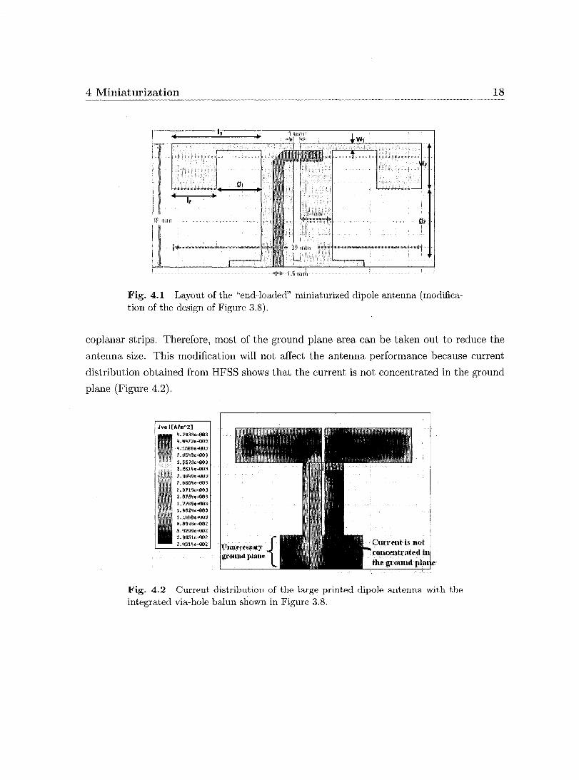
4.2 Removal of the unnecessary ground plane
Note that the large ground plane at the input of the microstrip line in Figure 3.8 is no
longer present in Figure 4.1. Since the dipole structure acts as the ground plane for the
microstrip feed line, there is no need to have a large ground plane at the end of the coplanar
strips in Figure 4.1. As mentioned in section 3.1.1, the quarter-wave coplanar strips form a
short-circuited stub. The ground plane only serves as a return path for the current on the
4 Miniaturization
Iz
19
41*!1>' 15 mm
Fig. 4.1 Layont of the "end-Ioaded" miniaturized dipole antenna (modification of the design of Figure 3.8).
18
coplanar strips. Therefore, most of the ground plane area can be taken out to reduce the
antenna size. This modification will not affect the antenna performance because current
distribution obtained from HFSS shows that the current is not concentrated in the ground
plane (Figure 4.2).
JYol[Mm~2]
1f.71t3SuOOa 4. ~~73".OO~ 4.1.!ia8e.OOS 3.1154$ •• <00$ 3. SSJa •• <oos 3.111114 ... <00$ 2.9649 •• <00$ 2. 8664 •• <0011 Z. 1171 9".<OOS 2 ,11154 •• <00" 1. 716\1<1.<003 L ~S24 •• <OO$ 1 •. 16!a~.'<OO$ a.M4$MOOZ 5.\1299 •• 002 2.9651e·d31Z12 2.4914.-002
UIUll'ttSSlU'V {
gl'olllul pianI'
Fig. 4.2 Current distribution of the large printed dipole antmma with the
integrated via-hole balnn shawn in Figure 3.8.

4 Miniaturization 19 ------_._- --------------
4.3 Simulation of the miniaturized "end-Ioaded" dipole antenna
The design in Figure 4.1 is simulated using Momentum and HFSS. The simulation setup is
almost the same as in section 3.1.2, except that in HFSS, the number of mesh refinement
cycles is increased from 3 to 5 to generate more accurate results. The antenna layout is
again drawn on two 0.017mm-thick copper strip layers in between the same Rogers HF
material R04350B. The length of the microstrip feed line and the coplanar strips (i.e. W2
+ 92) are approximately quarter-wavelength at the resonant frequency. The length of the
dipole arms (h) is less than quarter-wavelength. h can be further reduced by using larger
met al plates (i.e. increasing W2 and l2). The parameters in Figure 4.1 are then optimized
using the simulators (Table 4.1).
The simulation results are shown from Figure 4.3 to Figure 4.5. The return loss of the
antenna is below -lOdB from 2.32GHz to 2.57GHz, resulting in a bandwidth of 250MHz
(Figure 4.3). The far-field radiation pattern is only roughly omnidirectional on the H-plane
(Figure 4.4). The antenna has a slightly higher gain towards the direction of the arms. The
front-to-back ratio is 0.57dB. The pattern modification is due to the usage of "end-loaded"
dipole arms that concentrate more current towards the direction of the arms. In contrast,
the pattern is perfectly omnidirectional in the preliminary designs (Figures 3.1 and 3.8)
because the current is distributed more evenly in the rectangular dipole arms. The antenna
has a peak gain of 2.85dB and efficiency of 99.4%. The cross-polarization level is less than
-25dB on the H-plane at 2.4GHz (Figure 4.5).
4.4 Comparison between the miniaturized "end-Ioaded" dipole
antenna and the preliminary design
The antenna performance of the miniaturized "end-loaded" dipole antenna (Figure 4.1) and
its larger counterpart (Figure 3.8) is summarized in Table 4.2. The miniaturized version is
60% smaller than but with performance comparable to the original printed dipole antenna
with via-hole balun. Its gain is the same and the efficiency is 13% higher than the larger
version. The radiation pattern is not perfectly omnidirectional but is still acceptable. The
cross-polarization level is also much lower, resulting in a more linearly-polarized antenna.
The only major disadvantage is the decrease in bandwidth. This drop is expected because
generally, "the thicker the dipole, the wider is its bandwidth" [8].

4 Miniaturization 20 -------------_._----_ .. _---_._---------------------------------
-5
-10
ai' :s-U;
-15
-20
-25L---~----~----~----~--~----~----~----~----L---~
1 1.2 1.4 1.6 1.8 2 2.2 2.4 2.6 2.8 3 Frequency (GHz)
Fig. 4.3 Simulated 5'11 for the miniaturized "end-loaded" printed dipole antenna of Figure 4.1.
330 30
90
210 150
180
-Towards the dipole arms o
330 30
270 f--Hf-+--+--+-~::-+---+--+-I--+----1 90
210 150
180
Fig. 4.4 Simulated E-plane and H-plane radiation patterns for the miniaturized "end-loaded" printed dipole antenna of Figure 4.1.

4 Miniaturization
iD ~ Q)
o
-10
-20
:a -30 'ë 0> ., ::;
-40
-50
-150 -100 -50 0 50 100 150 200 Theta (deg)
Fig. 4.5 Co/Cross polarization level for the miniaturized "end-Ioaded" printed dipole antenna of Figure 4.1.
Table 4.2 Comparison between the miniaturized "end-Ioaded" dipole antenna (Figure 4.1) and its larger version (Figure 3.8).
21
Antenna Performance Miniaturized "end-Ioaded" dipole Large dipole with via-hole balun
Gain 2.85dB Efficiency 99.4% Cross-polarization level -25.~}5dB
Bandwidth 250MHz Dimension 7.41cm2
2.84dB
86.0% -1~}.85dB
700MHz 17.39cm2

22 -_ .. _---------_._--------------------
Chapter 5
Bandwidth Enhancement
Although the miniaturized "end-loaded" dipole antenna has performance comparable to
the large preliminary designs, the latter's broadband characteristic is lost in the compact
version. The bandwidth has dropped from 700MHz (for the original design with large dipole
arms in Figure 3.8) to 250MHz (for the compact design in Figure 4.1). As mentioned in
Section 4.4, this decrease is somewhat expected, since the bandwidth is proportional to
the width of the dipole arms [8]. Although the 250-MHz bandwidth is sufficient for many
applications (e.g. the Zigbee transceiver that is used for testing in later sections just
requires a lOO-MHz bandwidth), it willlimit its use for large bandwidth applications. We
hence discuss possibilities of bandwidth improvement next.
Modifying the shape of the radiating elements of dipole antennas to obtain wider band
width has been studied in the pasto Examples include tapered elements, bunny-ear ele
ments, and bow-tie antennas [23, 24]. However, many solutions require a drastic change
of the whole antenna structure. Further, the usage of the irregularly shaped structure
(e.g. bunny-ear) not only increases the complexity of the design, but also increases the
overall design size. The solutions proposed here use only regular shaped elements without
significant modification of the overall antenna structure.
5.1 Usage of tapered dipole arms
The first technique for bandwidth enhancement resorts to the use of tapered dipole arms
as the radiators. Modifying the shape of the radiating elements to obtain wider bandwidth
has been reported in the literature to date. Examples include bunny-ear elements [25]
2005/07/26

5 Bandwidth Enhancement 23
and bow-tie antennas [24J. In the work presented here, the tapered arms are created by
inserting triangular elements between the plates and the coplanar strips (Figure 5.1).
Tapered anns create b y Îll ~el·tioll of ' tI'iangular eleme'llts
19 mm
Omm
'mm
Fig. 5.1 Layout for the "end-loaded" printed dipole antenna with tapered arrns for bandwidth enhancernent.
The usage of tapered arms will increase the resonant frequency Jo of the antenna.
Increasing the dipole arm lengths can revoke this effect at expense of larger antenna size.
An alternative solution is to widen the tapered arms. Referring to Table 4.1 in Section
4.4, widening the met al plates (i.e. increasing W2 in Figure 4.1) can increase Jo without
changing the overall size of the antenna..
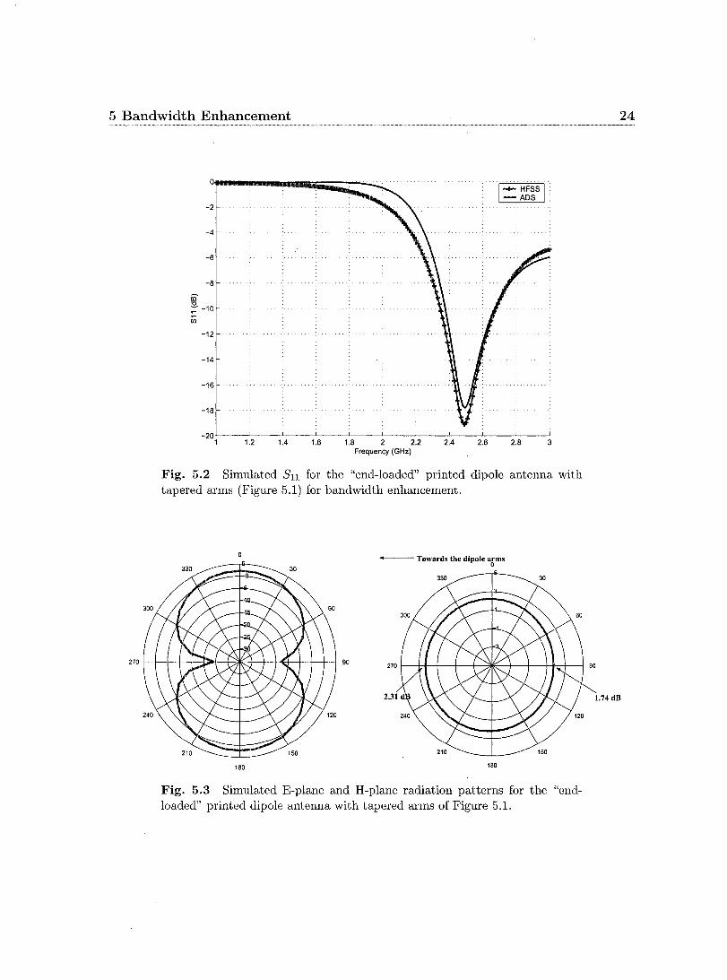
The design in Figure 5.1 is simulated using Momentum and HFSS. The simulation setup
is almost the same as in section 3.1.2, except that in HFSS, the number of mesh refinement
cycles is increased from 3 to 8 to generate more accurate results. The simulation results
are shown from Figure 5.2 to Figure 5.4. The return loss of the antenna is below -lOdB
from 2.35GHz to 2.67GHz, resulting in a bandwidth of 320MHz (Figure 5.2). Similar to the
"end-loaded" dipole antenna, the far-field radiation pattern is only roughly omnidirectional
on the H-plane (Figure 5.3). The antenna has a slightly higher gain towards the direction
of the arms. The front-to-back ratio is O.57dB. The antenna has a maximum gain of 2.91dB
and efficiency of 99%. The cross-polarization level is less than -25.79dB on the H-plane at
2.4GHz (Figure 5.4).
5 Bandwidth Enhancement
-2
-4
-6
-8
âl :!?. ~
-10
Cii -12
-14
-16
-18
-20 1 1.2 1.4 1.6 1.8 2 2.2 2.4 2.6 2.8 3
Frequency (GHz)
Fig. 5.2 Simulated 8 u for the "end-loaded" printed dipole antenna with tapered arms (Figure .5.1) for bandwidth enhancement.
--Towards the dipole a~ms
330 30
270 1-11-1--t-t--,t;ilII*-+,,*o-t--+--t-<E+--t--t-+-1 90
180 180
Fig. 5.3 Simulated E-plane and H-plane radiation patterns for the "endloaded" printed dipole antenna with tapered anus of Figure 5.1.
24

5 Bandwidth Enhancement
-50 0 50 100 150 200 Theta (deg)
Fig. 5.4 Co/Cross polarization level for the "end-loaded" printed dipole antenna with tapered arms (Figure 5.1) for bandwidth enhancement.
5.2 Combination of two techniques: Parasitic elements and
Tapered dipole arms
25
The technique of the previous section can increase the bandwidth by 70MHz (to approxi
mately 320MHz). A wider bandwidth of approximately 500MHz can be achieved by ad ding
parasitic elements to the tapered dipole arms introduced in the last section. The concept
is inspired by the design in [26] in which a rectangular parasitic element is placed near the
dipole arms. The latter's electric field is cou pIed to the parasitic element, which becomes
a radiator itself. This parasitic element is designed to have a length slightly different from
the dipole arms to create extra resonance that increases the bandwidth of the antenna.
Applying the same concept here, two thin lines (which act as parasitic elements) are
added along the edges of the tapered arms (Figure 5.5). These lines and the dipole arms are
placed on the same side of the substrate. The width of the gap between the dipole arms and
the thin lines is used to control the coupling effect. A narrow gap generates more coupling
but it raises difficulty of the manufacturing process. Optimization using Momentum and
HFSS shows that a gap of O.4mm presents a good compromise. The length of these thin lines

5 Bandwidth Enhancement 26
can be used to control the second resonant frequency. Such modifications are illustrated in
the design of Figure 5.5.
Fig. 5.5 Layout for the "end-loaded" printed dipole antenna with tapered arms and parasitic elements for bandwidth enhancement.
The simulated return loss for this antenna with increased bandwidth is shown in Figure
5.6. The return loss of the antenna is below -10dB from 2.3GHz to 2.8GHz, resulting in a
bandwidth of approximately 500MHz. Notice that the resultsfrom the two EM simulators
are slightly different from each other. The first resonant frequency given by HFSS is about
70MHz lower than the one obtained from ADS. As mentioned in Chapter 2, due to the
usage of infinite substrate in calculations in ADS, any surface wave bounced back from the
edges will not be considered, thus introducing errors into the calculation of the resonant
frequency [19, 20].
Similar to the design with the tapered arms only, the far-field radiation pattern of
this antenna is roughly omnidirectional on the H-plane (Figure 5.7). The antenna has a
slightly higher gain towards the direction of the arms. The front-to-back ratio is increased
to 1.11dB. This modification in the pattern is expected due to the presence of the two
thin lines (parasitic elements) and the wide tapered arms, which cause uneven current
distribution near the front side of the antenna. The antenna has a maximum gain of
2.84dB and efficiency of 99.4%. The cross-polarization level is less than -22.3dB on the
H-plane at 2.4GHz (Figure 5.8).

5 Bandwidth Enhancement
-5
-10
Cil ~
èii -15
-20
-25~--~----~--~L----L----~--~----~----~--~----~
1 1.2 1.4 1.6 1.8 2 2.2 2.4 2.6 2.8 3 Frequency (GHz)
Fig. 5.6 Sirnulated S11 for the "end-loaded" printed dipole antenna of Figure 5.5 with tapered arrns and parasitic elements for bandwidth enhancement.
270 f-+--+--+--BiIfit-~~f--*+-+--t--I 90
210 150
180
- Towad. the dipole arm. o
330
210
180
30
150
Fig. 5.7' Sirnulated E-plane and H-plane radiation patterns for the "endloaded" printed dipole antenna with tapered arms and parasitic elernents of Figure 5.5.
27

5 Bandwidth Enhancement
-150 -100 -50 0 50 100 150 200 Theta (deg)
Fig. 5.8 Co/Cross polarization level for the "end-Ioaded" printed dipole antenna with tapered arms and parasitic elements (Figure 5.5) for bandwidth enhanc:ement.
5.2.1 Alternative design: Parasitic elements on opposite side of the tapered
arms
28
An alternative version of the design of Figure 5.5 is shown in Figure 5.9. Triangles are
still inserted between the copi anar strips and the metal plates to form tapered arms. How
ever, the parasitic elements along the edges of the tapered arms are printed on the di
electric surface opposite to that of the antenna structure, facilitating for a more compact,
space-saving design. Current experiments suggest that additional overlap on the opposing
substrate sides will decrease the second resonant frequency, which demonstrates additional
flexibility of the design. The final bandwidth obtained by this alternative design is still
approximately 500MHz (Figure 5.10), which is the same as the design of Figure 5.5. The
antenna has a maximum gain of 2.96dB and efficiency of 99.4%. The cross-polarization
level is less than -19.8dB on the H-plane at 2.4GHz (Figure 5.8), which is almost 2.5dB
higher than the design in Figure 5.5.

5 Bandwidth Enhancement -------_. __ ._---_ .. _-----_ .... _--------_ ...... -
mm
Fig. 5.9 Alternative design of Figure 5.5 with parasitic elements on opposite side of the tapered arms.
-5
-10
iil "0 ;: -15
èii
-20
-25
_30L-__ ~ ____ ~ ____ ~ __ _L ____ ~ __ ~ ____ _L ____ ~ __ ~ ____ ~
1 1.2 1.4 1.6 1.8 2 2.2 2.4 2.6 2.8 3 Frequency (GHz)
Fig. 5.10 Sirnulated 8 11 for the design of Figure 5.9 with parasitic elements on opposite side of the tapered anns.
29

5 Bandwidth Enhancement
--Towards Jhe dipole arms
90 270 1-----H1--+--+--f--'::lI!E--+--+--+i-+_---1
180 180
Fig. 5.11 Simulated E-plane and II-plane radiation patterns for the design of Figure 5.9 with parasitic elements on opposite side of the tapered arms.
00 :s CI)
o
-10
-20
~ -30 '2 Cl
'" ::;:
-40
-50
-150 -50 a Theta (deg)
50 100 150 200
Fig. 5.12 Co/Cross polarization level for the design of Figure 5.9 with parasitic elements on opposite side of the tapered anns.
30
90

5 Bandwidth Enhancement
5.3 Summary of the results from aIl designs
Table 5.1 Results of the antennas using different bandwidth enhancement techniques
Antenna Broadband Miniaturized Dipole Dipole with Dipole with
Performance dipole with "end-loaded" with tapered anns tapered arms
via-hole dipole tapered and parasitic and parasitic
balun (Fig 4.1) arms elements elements on (Fig ~).8) (Fig 5.1) (Fig 5.5) opposite si des
of substrate
(Fig 5.9)
Gain 2.84dB 2.85dB 2.91dB 2.84dB 2.96dB
Efficiency 86.0% 99.4% 99.0% 99.4% 99.4%
Cross-polar. -13.85dB -25.~~,5dB -25.79dB -22.:3dB -19.8dB
Bandwidth 700MHz 250MHz 320MHz 500MHz 500MHz
31

32 -------
Chapter 6
Pattern correction
In addition to the bandwidth, the radiation pattern of an antenna is also important for
most wireless applications. The miniaturized "end-Ioaded" dipole antenna (Figure 4.1) has
the typical "doughnut" shaped 3-D polar pattern of an ideal dipole antenna (i.e. omnidi
rectional pattern on the H-plane). This omnidirectional pattern (Figure 4.4) is desirable
because the antenna can emit or receive the same amount of power at an directions on an
horizontal plane (H-plane). The disadvantage is that the gain is only moderate and the
E-plane pattern has two nuns along the direction of the dipole arms. Simulation results
show a difference of approximately 30dB between the peak gain and those at the nuns
(Figure 4.4).
6.1 Usage of bent dipole arms
In real applications, the nuns are undesirable because they create blind spots. Several
simple design techniques have been used to cancel these nulls. They include the usage
of "broken arrow" shaped radiators or bending the tip of the dipole arms inward by 45 0
[27]. Applying the same techniques to the miniaturized "end-Ioaded" dipole antenna, the
thin lines and the met al plates are bent inward to cancel the nuns at 90 0 and 270 0 on the
E-plane (see Figure 6.1). The bending angle is optimized using the two EM simulators.
Experiments show that a larger bending angle can increase the gain further at the nuns
in exchange of slightly narrower bandwidth and lower peak gain. A bending angle of 30 0
presents a good compromise here.
The design of Figure 6.1 is simulated using Momentum and HFSS. The simulation setup
2005/07/26

6 Pattern correction 33
is almost the same as in section 3.1.2, except that in HFSS, the number of mesh refinement
cycles is increased to 8 to generate more accurate results. The effects of the bent dipole
arms on the nulls are clearly shown in the E-plane radiation pattern (Figure 6.2). The
gain at the null at 90 0 is increased from -15.7dB to -9.3dB. The gain at the second null at
270 0 is increased from -34.3dB to -12.3dB. To illustrate the effects of the bent arms on the
overall antenna performance, the results of two antennas with different bending angles are
summarized in Table 6.1, with results of the original "end-loaded" dipole for comparison.
: 19 nm
Fig. 6.1 Modified design of "end-loaded" dipole antenna of Figure 4.1 with arms bending inward by 30 o.
Table 6.1 Results of the antennas with different bending angles
Antenna "End-loaded" dipole 1 Dipole with 20 0 1 Dipole with 30 0
Performance without bent arms bent arms bent arms
Max. Gain 2.85dB 2.76dB 2.67dB Efficiency 99.4% 99.3% 99.2% Cross-polar. -25.35B -16.97dB -14.58dB Bandwidth 250MHz 240MHz 220MHz Gain at nulls -15.69dB -12.28dB -9.33dB (90 0 and 270°) -34.30clB -16.46dB -12.28dB
6.2 Usage of asymmetrical coplanar strips
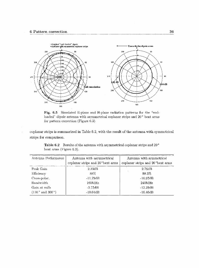
The gain at the nulls can be further increased by using asymmetrical coplanar strips (Figure
6.3). Symmetrical coplanar strips are not mandatory but they facilitate the design process,

6 Pattern correction
o + With bent dipole arms - Without bent dipole arms 30
270 r-t-t--jf-~±::~~~T++~=-*-j--t---j 90
180
Fig. 6.2 Null cancelation on the E-plane pattern due to the usage of 30 0
bent dipole arms (Figure 6.1).
34
especially for the antenna with the J-shaped balun (Figure 3J). In that design, sin ce the
coplanar strips serve as the ground plane for the microstrip line and the open-circuited
stub, their width is dependent on those two elements.
Using the via-hole balun, the open-circuited stub is avoided and the right part of the
coplanar strips in Figure 6.3 can be partially removed. The narrower strip on the right
si de now acts as a current choke that forces more current into the right dipole arm and
eventually increases the gain at the null at 90 0• The strong current concentration on the
right arm is clearly depicted in Figure 6.4. The resulting radiation patterns are shown in
Figure 6.5. With the asymmetrical strips, the E-plane pattern is slightly tilted such that
the nulls (i.e. minimum gain) occur at 110 0 and 300 0• The gain at these nulls is now
increased to -5.75dB and -10.04dB, respectively.
6.2.1 Disadvantages of the asymmetrical coplanar strips
Null cancelation is obtained at the expense of narrower bandwidth, lower efficiency, higher
cross-polarization level, and lower peak gain. In addition, the radiation pattern changes
slightly with frequency (Figure 6.6). The performance of the antenna with asymmetrical

6 Pattern correction
Fig. 6.3 Modified design of the antenna in Figure 6.1 with asymmetrical coplanar strips and 20 0 bent anns
Jsurf[M,,]
11 .. 51118+001 ;t.416!36~1
~ _m~ !:~~~;:= .1.1337",..001 1,(f39"t~~1
,).'iW!h~~
a.S€i66~~
7.56$$lf~_
1S.619ge~
$.aj'ailte~
't,7329g~
$. 7:l39ltl!4000 2.81tSgt;tOO)
L'302'1te+BOO 9 • .5893e'-OO1
1.S1j.39e-002
Fig. 6.4 Curront distribution of the antenna of Figure 6.3 with asymmetrical eoplanar strips. Strong current concentration on the 20 0 bent right arm cancels the null at 90 0 on the E-plane.
35
6 Pattern correction 36
-Original "cml-loaded" dipole +Antenna 'Oith a.ymmctric coplanar .trips Toward~ the dipole arms
330 30
270 f----+-:-H-+--+---"~_+_-f----+-__+__I 90
210 150
180 180
Fig. 6.5 Sirnulated E-plane and H-plane radiation patterns for the "endloaded" dipole antenna with asyrnrnetrical coplanar strips and 20 0 bent arms for pattern correction (Figure 6.3).
coplanar strips is summarized in Table 6.2, with the result of the antenna with symmetrical
strips for comparison.
Table 6.2 Results of the antenna with asyrnmetrical coplanar strips and 20 ° bent arrns (Figure 6.3).
Antenna Performance 1 Antenna with asymrnetrical coplanar strips and 20 °bent arms
Peak Gain Efficiency Cross-polar. Bandwidth Gain at nulls (110 0 and 300°)
2.33dB
88% -11.79dB
160MHz
-5.75dB -1O.04dB
Antenna with symmetrical coplanar strips and 20 0 bent anns
2.76dB
99.3%
-16.97dB
240MHz
-12.28dB
-16.46dB

6 Pattern correction
o
330 30 - 2.40 GHz + 2.44 GHz -0- 2.48 GHz
270 f--t--CJ'I4"'-t--t--:1)C--t--t--F-l-+--G-t---l 90
210
180
Fig. 6.6 Simulated E-plane radiation pattern for the antenna with asymmetrieal eoplanar strips (Figure 6.3) at different frequeneies. The pattern is ehanging with frequeney.
37

Chapter 7
Integration of antenna units within
wireless networks
38
The characteristics of the printed dipole antennas are discussed in Chapter 3. Several
improvement techniques on the antennas are presented in Chapt ers 4, 5, and 6. In this
chapter, one of the proposed antenna designs is integrated with a Chipcon IEEE 802.15.4
(Zigbee) wireless transceiver [28] on the same PCB to examine its functionality in wireless
networks. The methodology for the integration and the related issues will be discussed.
The effects of the feeding network on the antenna performance will also be studied.
External antennas are often fragile and they increase the complexity and manufacturing
costs of wireless devices. Recent advances in CMOS integrated circuits have allowed the
integration of an RF front-end onto the same die as the digital demodulation and media
access control components. Since printed microstrip antennas are compatible with the
printed circuit fabrication techniques [8], they can be used to replace the external antennas
at the expense of sorne PCB area. Subsequent to the integration, the antenna performance
may be impaired by nearby components in the circuits. Careful design methodology that
avoids interference with the rest of the system is therefore necessary.
7.1 Requirements
The following sections summarize the requirements of the antenna for the operation of the
IEEE 802.15.4 (Zigbee) wireless transceiver [28].
2005/07/26

7 Integration of antenna units within wireless networks 39
7.1.1 Operating frequency and bandwidth
Similar to most wireless applications, the Zigbee wireless transceiver uses the instrumen
tation, scientific and medical (ISM) frequency bands that do not require the band-usage
license. This band has a center frequency Je at 2.45GHz and spans frequencies from iL =2.4GHz to lu =2.5GHz. The bandwidth of the integrated antenna must at least coyer this
frequency range, but not overly exceed it, to avoid the consequent noise. In the standpoint
of Electromagnetic Compatibility (EMC), using a resonant antenna (e.g. printed dipole
antenna) with an adequate bandwidth will reject the interference coming from the rest of
the system and will not exacerbate the EMC emissions present in other parts as long as the
system clocks on the board are in frequency far from the center frequency le. Indeed, this
is the case in practice, where common microcontrollers run at clock rates that are orders
of magnitude lower.
7.1.2 Impedance mat ching
From the data sheet of the Zigbee transceivers [28], the RF input/output port is differential
with an optimum differentialload of 115+j180 D. The simplest configuration is to connect a
differential (i.e. balanced) antenna directly to this port. However, as mentioned previously,
most vector network analyzers (VNA) are incapable of differential measurement [16J. Thus,
a balun circuit implemented with low-cost dis crete inductors and capacitors is used to
convert the differential RF port to a single-ended 50-D port (This balun is given by the
data sheet of the transceiver [28]). In this way, single-ended (i.e. unbalanced) antenna can
be used. The input impedance of the antenna must be matched to the 50-D port to ensure
optimal power transfer to/from the transceiver. Power efficiency is important because most
wireless devices are powered by small batteries; an efficient antenna can extend the battery
life by reduced energy emission for the same distance.
7.1.3 Selection of the dielectric substrate material
The dielectric constant Cr (Le. permittivity), the 10ss tangent tan 6, and the thickness of
the dielectric substrate aIl have noticeable impact on the integrated antenna. Generally,
using a thicker substrate will widen the bandwidth of the antenna (p.158, [21]). However,
if the thickness is larger than 180' there will be more spurious radiation and surface wave
excitation, which will eventually decrease the efficiency. In contrast, employing a substrate

7 Integration of antenna units within wireless networks 40
with a high dielectric constant Cr will give a narrower bandwidth. Although the higher
dielectric constant has the advantages of size reduction and higher quality factor (Q), it
also has the "drawbacks of easily excited surface waves, lower bandwidth, and degraded
radiation efficiency" [21, 22]. Lastly, the dielectric loss tangent tan 0 primarily affects the
antenna efficiency. High values of tan 0 imply that sorne power will be lost in the dielectric,
reducing the gain of the antenna. Experiments imply that the Rogers HF material R04350B
shows a good compromise of aU mentioned parameters and is chosen for the substrate
material. It has a thickness of 0.762mm, a dielectric constant (cr) of 3.48 and a loss
tangent of 0.0031.
We note that many PCBs are printed on the inexpensive fiberglass-based FR4 material
to reduce the manufacturing cost, especiaUy for low-volume applications. It is therefore
beneficial to study the option of using FR4 material for the substrate.
Table 7.1 peB materials electric properties
Material 1 thickness (mm) 1 tan 6 1 Cr 1 Cr tolerance
FR4 1 0.762 R04~{50B 1.5748
1
0.013 1 4.2-4.8 1 13.f.i% o.oo~n 3.48 2.8%
Major differences between the two materials are summarized in Table 7.1. FR4 material
is more than two times thicker than the Rogers RF material. The former also has a loss
tangent that is four times larger. These differences will affect the performance of the new
design. The advantage of using a thick dielectric is that the bandwidth of the antenna
is increased [21]. Since the IEEE 802.15.4 standard is not a wideband application (only
100MHz), this enhanced bandwidth is not necessary. In contrast, higher loss tangent and
higher Cr tolerance of the FR4 material are undesirable because they contribute to energy
loss and inaccuracy of the simulation models.
7.2 Design methodology overview
The design flow of the integrated antenna is depicted in Figure 7.1. Based on the require
ments mentioned in the last section, the miniaturized "end-loaded" printed dipole antenna
(Figure 4.1) is chosen due to its adequate bandwidth (250MHz), high efficiency (99.4%),
omnidirectional pattern, linear polarization, and flexibility in frequency tuning.

7 Integration of antenna units within wireless networks 41
7.2.1 Development of simplified model for fast simulation
To refiect the changes of the antenna performance subsequent to the integration, the "end
loaded" dipole in Figure 4.1 must be modified. At this stage of the design, accurate
modeling of the rest of the board is not yet required. Hence, all the details of the electronics
are removed, except for the bot tom ground plane required for modeling its effect on the
antenna (Figure 7.2). The presence of the long PCB ground plane su ms up the undesired
coupling effects from all components near the antenna. It is unnecessary to model the
whole ground plane because current density drops significantly in area far from the antenna.
Thus, only part of the ground plane (lOmm) is attached to the input of the antenna to
reduce simulation time. This simplified model is simulated using the 2.5-D EM simulator
Momentum, in which the parameters (gl, g2, W1, W2, h, l2) in Figure 7.2 are optimized
according to Table 4.l.
When simulations confirm the validity of the antenna, a PCB is etched using rapid
prototyping methods. Etching accuracy is not too important as an inaccuracy of O.5mm
in the length of the half wave dipole will translate in a frequency shift of rv17MHz. PCB
processes can achieve much higher accuracy.
Lab measurement is next performed on the test antenna to ensure that all the modeling
is correct and that no unexplained mismatch exists between the lab results and simulation
model. The microstrip feed line is extended to reach the edges of the board such that an
end-Iaunch SMA connector can be mounted as a test port. The latter is connected to an
HP vector network analyzer to measure the return loss (S11) across the operating frequency
range. The use of specialized RF laminates (e.g. Rogers HF material R04350B) in general
shows excellent correlation between lab results and simulation models, but this step is
critical if the material like FR4 is used to ensure a good fit with the simulation. When
there is significant mismatch, the initial antenna design will be modified, re-simulated, and
retested again, until it satisfies all the requirements. At that point, the PCB layout for
the rest of the board can include the simplified antenna model in the PCB database. The
antenna is at this stage given as a PCB route and plane obstruct zone constraint, to be
replaced later with the final model.
As the PCB layout is nearing completion, it is extracted and prepared for a full 3-D
EM simulation, yielding in a more precise analysis. At this point, battery and enclosure
models may be inserted into the 3-D model to ensure that their presence in the design does

7 Integration of antenna units within wireless networks 42
not "de-tune" the antenna and to characterize their effect on the radiation pattern. Wh en
the peE model is imported in the 3-D EM simulator HFSS with the integrated antenna,
digitallines and other non-RF signaIs can be removed since they do not affect the antenna;
doing so will significantly speed up the simulation. On the other hand, the extraction must
preserve the via connections that link the top and bottom planes near the antenna and
feed line.
L_
Initial Antenna Selection Based on Bandwidth. Center Frequency and Polarization
SizeBasiestructute
2.50sirnliÏlà1îons Ràâiatio.n.p.m AOàlysis
Test AntennaFabtication Lab Measurerhents {S11)
PCBLayout Reserve Antehna Arêas
LocateLarge Elements.Away from An~enn~
LilY àùFEleC1r ...... ;I;t~fI~verJs~.~,ound
Via ConneètTop~BQttom
Extracf PCSMol.1el Importîn 3D RF.~b:rl1.;1lator
•.... .Sil11plity Oigit.~lGWéûit .. . ' M(jdel Làr:-ge CPl11ponè~l§Ind Enclosure
Check ~EtSonnant I!=requency ~lleckJ:\ntenna p~~ef:!l and'ÊfJfClI@i,1dY •
PCB Manufacturing and Test
Fig. 7.1 Design flow of the integrated antenna. The full arrows show the order of the design process. The dashed arrows designate the optional cycles that are perforrned if there is significant mismatch between the lab results and the simulation model.
7.2.2 Simulation results of the simplified model
The simplified model of Figure 7.2 is simulated using Momentum and HFSS. The simulation
setup is almost the same as in section 3.1.2, except that in HFSS, the number of mesh

7 Integration of antenna units within wireless networks
1 18 mm!
l 10 mm
GI'o:mu11lmlt t!l~t ~llm, UI)
tfft'ds of ail nelu'by 0 jtcts
Fig. 7.2 Simplified mode! for fast simulation: Layout of the "end-Ioaded" miniaturized dipole antenna with large ground plane that surns up the effect of nearby abjects on peB (modification of the design in Figure 4.1).
43
refinement cycles is increased from 3 to 9 to generate more accurate results. The results
are shown in Figure 7.3 and Figure 7.4. Simulation results show that the the bandwidth is
reduced to 150MHz with the addition of the PCB ground plane. In addition, the radiation
patterns of the antenna are no longer omnidirectionaL According to the Image Theory, the
si de facing the ground plane (i.e. towards the dipole arms) will have stronger field due to
the reflection from the ground plane [8]. This is clearly shown in the radiation patterns in
Figure 7.4. The front-to-back ratio is almost 12.23dB.
7.3 Effects of the PCB on the antenna performance
Although the performance of the simplified model is slightly degraded due to the presence
of the PCB ground plane, it is still acceptable for the Zigbee application. The next step
is to etch the antenna structure of Figure 7.2 on a PCB using rapid prototyping methods.
The resulting antenna is tested and the measurement result is shown in Figure 7.3. The
difference between the resonant frequencies of the real antenna and the simulation model
is less than 1% (20MHz). Since there is no significant mismatch between the test antenna
and the simulation model, the next step is to integrate this antenna into the complete PCB
model of the Zigbee transceiver unit. The latter is exported from the Mentor Expedition
PCB tool set ta the 3-D EM simulator HFSS. The 3-D PCB model with the integrated

7 Integration of antenna units within wireless networks
t
Or-----~-----,-----,,_----,_----_r----_.------._----,
-10
-20
co ::- -30
èii
-40
-50
2.25 2.3 2.35 2.4 2.45 2.5 2.55 2.6 Frequency (GHz)
Fig. 7.3 Simulated Su for the simplified model with large PCB ground plane of Figure 7.2. Measurernent of the real antenna is also shown for cornparison.
5.76 dB 0
330 30
-Towards the dipole arm o
Towards the dip 300
270 1-1-1-1-1-P"-kHI!E:-I-I-k"-I-I-I-H 90 270 1--7--t--t---+-~;;,-ft--t--+-t---j 90
210 150 210 150
180 180
Fig. 7.4 Sirnulated E-plane and H-plane radiation patterns for for the simplified model with large PCB ground plane of Figure 7.2.
44

7 Integration of antenna units within wireless networks 45
antenna is shown in Figure 7.5.
7.3.1 Reduction of parallel-plate mode using via-holes
Since the "end-Ioaded" printed dipole antenna is extended directly from the Zigbee trans
ceiver board, the latter will certainly affect the antenna performance. In addition, the
ground plane of the board has a direct effect on the antenna because the coplanar strips
and the di pole arms are extended from the ground.
To fulfill the routing requirements, the Zigbee transceiver is built on a two-Iayered PCB
(the Chipcon transceiver data sheet even recommends a four-Iayered PCB layout [28]). The
top layer is used for signal and power routing. The bot tom layer is used as the ground
plane. Like most multi-Iayered boards, these two layers act as a microstrip patch antenna
and generate undesired radiations [20, 29, 30]. To avoid this problem, the open areas of the
top layer are filled with vias connected to the ground (Figure 7.5). These vias are necessary
to suppress the parallel mode that may exist between the two layers. Without the vias,
part of the power fed to the antenna is launched into the parallel mode. This will result
into extra resonances that distort the passing band of the antenna [10]. AIso, the radiation
pattern will be affected.
The effectiveness of the vias depends greatly on their placements on the PCE. Since the
parallel-plate mode and the fringing field of the patch antenna are both excited near the
edges of the two conducting layers, the vias must be placed near these edges to suppress the
mode [20]. Moreover, the vias should be placed as close together as possible to be effective.
The general rule suggests that the spacing between any two vias should be less than half
wavelength to avoid the resonance of the parallel-plate mode [30]. Applying this rule, the
extra resonances of the parallel-plate mode disappear from the passing band.
7.3.2 Change in radiation patterns
The design of Figure 7.5 is simulated using HFSS. The simulation setup is the same as in
section 3.1.2. The results are shown in Figures 7.6 and 7.7. The return loss is less than
-lOdB from 2.32GHz to 2.49GHz, resulting in a l70-MHz bandwidth. This is close to the
bandwidth predicted by the simplified model.
The most notable effect of the PCB's presence is the change in gain and radiation
patterns. The patterns of the integrated antenna are no longer omnidirectional (Figure

7 Integration of antenna units within wireless networks 46
Fig. 7.5 Complete PCB model with the integrated dipole antenna.

7 Integration of antenna units within wireless networks 47
7.7). The H-plane pattern shows that the radiation on the side of the antenna dominates
in power over that on the the PCB side. This can be quantified by the front-to-back (i.e.
antenna-side to PCB-side) ratio of 2dB. Further, we note two low-Ievel points (-4.5dB) at
120 0 and 240 0 (see Figure 7.7). As mentioned previously, the PCB ground plane acts as
a refiector, distorting the overall radiation pattern, as is predicted by the Image Theory of
antenna radiation in the vicinity of a perfectly conductive ground plane [8]. Consequently,
the received and the transmitted power will also peak in the direction on the antenna
side (rv3.6dB). The main advantage of the described scenario is the increase in peak gain.
Further gain increase can be achieved by distorting the ground plane to the shape of a
corner refiector or bending the metal plates and the thin lines inwards by 30 o.
7.3.3 Comparison between the simplified mode} and the integrated antenna
Comparing the results of the simplified model (Figure 7.2) and the integrated antenna
(Figure 7.5), the former model generally predicts correctly the behavior of the integrated
antenna. The major difference between the two models is their radiation patterns. Though
both designs predict non-omnidirectional patterns, the simplified model has a large front
to-back ratio (12.23dB) whereas the complete PCB model (with the integrated antenna)
only has a ratio of 2dB. This huge difference is due to the in complete PCB ground plane of
the simplified model. The incomplete ground plane is used to save simulation time in the
early stage of the design. Thus, once the performance of the simplified model is validated,
it is necessary to simulate the complete PCB model (with the integrated antenna) to obtain
the correct radiation patterns.
7.4 Measurement and results
7.4.1 Return 10ss
The last stage is to fabricate the Zigbee board with the integrated antenna on Rogers HF
material R04350B. The return loss of the antenna is measured using an HP 8593E Vector
Network Analyzer through a SMA connectoI. The close match between measurement and
the HFSS simulation results is shown in Figure 7.6. The return loss is less than -10dB
from 2.275GHz to 2.475GHz, resulting in a bandwidth of 200MHz. Since the operating
frequency range of the transceiver is from 2.4 to 2.485GHz, the resonant frequency of the

7 Integration of antenna units within wireless networks
1 Towou',ls t1 .. anttmlll
-5
-10
iD ~ -15 èij
-20
-25
-30 2L--2-,'.I,-----::2'=.2-~2.3:----::2L.4-~2.=-5 ---:2:':.6--:'2.=-7 ---:2:':.8-----::'2.'="9----'
Frequency (GHz)
Fig. 7.6 Return 108s (S11) of the integrated antenna of Figure 7.5.
+ Simulllted
- l\IellSUI'NI 1 Tow .. 'ds the nnttluUl
Z70 f-+--+-+.:,;p+-+-'*'----)-+---HPII---1---1 80
'80 180
+ Simuhlted
- l\lcllsured
Fig. 7.7 Normalized E-plane and H-plane radiation patterns for the integrated antenna of Figure 7.5.
48

7 Integration of antenna units within wireless networks 49
antenna must be tuned slightly by cutting small part of the metal plates to completely
coyer that range.
7.4.2 Radiation patterns
Generally, radiation patterns are measured in an anechoic chamber. However, to show the
antenna patterns in a typical room environment, a different setup is chosen (Figure 7.8).
The emitted power from port 1 of the spectrum analyzer is transmitted by a standard
dipole antenna and is received by the integrated antenna, which connects to port 2 of the
analyzer. The return power received from different angles formulates the antenna pattern.
The normalized measured patterns (E-plane and H-plane) match closely to the simulated
ones (Figure 7.7). The slight discrepancy is due to the undesired scattering caused by the
turntable and various metallic structures in the room.
81) ertrum Allal:y·zer
Port 1 Port 2
Standard Dipole Anten:n.a.
Antenlla lImler test
Turntable
Fig. 7.8 The radiation pattern measurement setup.

50
Chapter 8
Balanced antennas and microwave
baluns
.In Chapter 7, we discuss the integration of the "end-loaded" dipole antenna with the Zigbee
wireless transceiver on the same PCB. As mentioned in Section 7.1.2, the RF input/output
port is differential (i.e. balaneed) with an optimum differentialload of 115+jI80 n. Renee,
a balun is needed to conne ct this differential RF port to the 50-n single-ended (i.e. un
balanced) port of the antenna. Sinee any additional deviee (including the balun network)
introduces losses into the system, it is worthwhile to study a complete differential setup
with the balun being removed and the single-ended antenna being replaeed by its differen
tial counterpart. In this chapter, the design of a balaneed dipole antenna is presented. The
difficulties of the differential measurement are also discussed. Finally, a new microwave
balun composed of transmission lines is proposed to improve the antenna performance in
the higher frequency range.
8.1 Design of the balanced dipole antenna
An antenna is balaneed if it can be fed directly by a differential port. The latter consists
of a pair of physical terminaIs that are fed with two signaIs with the same amplitude
but the opposite polarity (180 0 phase differenee). According to the data sheet of the
Chipcon CC2420 Zigbee RF transceiver [28], if a balanced antenna is used, no balun network
is needed. Sinee the balun network provided by the transeeiver is composed of discrete
inductors and capacitors, removing them will eertainly reduce the size and the fabrication
2005/07/26

8 Balanced antennas and microwave bal uns 51
cost of the final product. In addition, most discrete components are imperfect (especially
at high frequencies) and introduce losses and uncertainty into the system; removing them
will improve the power transfer efficiency from the transceiver to the antenna. Generally,
balanced devices are considered more immune to noise than their unbalanced counterparts
because noise cornes from the same source will have zero phase difference and appears as
common-mode signaIs. These signaIs will be blocked by differential devices that operate in
the differential mode [16].
With all the mentioned advantages, balanced antennas seem to be the ideal choice for
this project. However, designing a balanced antenna involves issues that must be first solved
to make a feasible design. Unlike single-ended devices that have standard impedances such
as 50-0, 75-0 or 300-0, differential components have no standard impedance value [16].
That means the antenna components must be custom-made in most cases. The lack of stan
dard port impedance also makes it difficult to calibrate the measurement plane of the VNA,
resulting in discrepancies in measurement. Lastly, measuring a 2-port balanced antenna
is more complex than measuring a simple single-port unbalanced antenna. Measurement
often requires software tools or physical baluns to obtain the differential S-parameters for
all ports. These issues will be discussed in the following sections.
To achieve maximum power transfer, the input impedance of the antenna should be
conjugately matched to the output impedance of the differential RF port. Thus, the ide al
input impedance of the antenna is the same as the optimum differential load given by the
data sheet of the transceiver, which is 115+j180 O. The reactance of this load is inductive.
According to the graphs of the calculated input impedance of the center-fed thin-wire dipole
antenna in [8], the reactive part becomes inductive when the total arm length is longer than
a half-wavelength. Further examination of the graphs implies that an arm length of 0.55>'
results in an input impedance close to the idealload impedance. Therefore, the first design
is based on the printed version of the thin-wire antenna (Figure 8.1).
8.1.1 Simulation setup and results
The design of Figure 8.1 is simulated using Momentum and HFSS. The simulation setup is
different from the previous chapters. In Momentum, instead of using the InternaI Port, a
pair of DifferentiaI Ports are connected to the two dipole arms of the antenna. In the Port
Editor, these ports must be set to associate with each other. The last step is important to

8 Balanced antennas and microwave baluns
25,41nm
71nln
Fig. 8.1 Balanced dipole antenna based on the center-fed thin-wire dipole antenna.
52
ensure a differential signal (with a phase difference of 180°) feeding into the antenna. The
port impedance is set to be 115-j180 D instead of 115+j180 D because the port must be
conjugately matched to the load impedance (i.e. 115+j180 D) in Momentum.
In HFSS, the Lumped-Port impedance is set directly to the load impedance (i.e. 115+j180
D), which is the opposite of the Momentum setup. In addition, the differential signal is
set by drawing a terminal line from one dipole arm to the other (See Figure 8.1). In a
single-ended design, the terminal line is normally drawn from the ground reference to the
conductor.
The antenna layout is drawn again on the 0.017-mm copper strip layer on top of the
dielectric substrate of Rogers HF material R04350B. The rest of the simulation setup is
almost the same as described in section 3.1.2, except that in HFSS, the number of mesh
refinement cycles is increased from 3 to 8 to generate more accurate results. The simulation
results are given in Figures 8.2 and 8.3.
The return loss generated by the two EM simulators are slightly different from each
other. Although the resonant frequencies are the same, the result given by HFSS has a
positive return loss (> OdB) from IGHz to 1.9GHz and beyond 3.1GHz (not shown in Figure
8.2). Generally, a positive return loss designates an unstable system that oscillates at that
frequency range. In this case, the positive return loss is due to the non-propagating mode
(also known as reactive or evanescent mode) of the virtual waveguide feeding the antenna
in HFSS simulation. This mode might be excited if the magnitude of the reactance is set
to be larger than the resistance of the input impedance [18]. The return loss is correct (i.e.

8 Balanced antennas and microwave baluns 53
< OdB) from 1.9GHz to 3.1GHz because this range is far from the cutoff frequency of the
virtual waveguide. The same problem does not exist in Momentum because Momentum uses
a different feeding method in simulation. Since the operating frequency of the transceiver
is outside the uncertain region, this will not be a problem for the Zigbee application.
The antenna has a return loss of less than -10dB from 2.3GHz to 2.7GHz and a cross
polarization less than -30dB. The efficiency is closed to 85% and its gain is about 2.0dB.
The gain is lower than the one of the unbalanced "end-Ioaded" dipole antenna with an
integrated balun (Figure 4.1) because the far-field radiation pattern is almost perfectly
omnidirectional on the H-plane (Figure 8.3). Except the lower (but still acceptable) gain,
this antenna satisfies aIl the requirements for the application and provides a complete
differential RF front-end.
5
0r-----------~--~~
-5
âl -10 :3-
Cii -15
-20
-25
-30
-35 '--_--'--_---'---_---'-__ '-----_-'--_-'--_----'-_--''----_-'--_....J
1 1.2 1.4 1.6 1.8 2 2.2 2.4 2.6 2.8 3 Frequency (GHz)
Fig. 8.2 The sirnu1ated return 10ss (Bn) of the ba1anced dipo1e antenna of Figure 8.1.
8.1.2 Disadvantage and alternative design
The only disadvantage of the antenna of Figure 8.1 is its relatively long dipole length
(52.8mm). This is set by the input impedance which requires a dipole length more than

8 Balanced antennas and microwave bal uns
330 30 330 30
270 1-+-+---t--+-+-:::;e!IIoi--3ll(E~a--t-+-I-t-+-t 90 270 1--I-+--+-+--+---3lI!E--+----t----t--!+---i 90
210 150
180 180
Fig. 8.3 Simulated E-plane and I-I-plane radiation patterns for the balanced dipole antenna of Figure 8.1.
54
half-wavelength long to remain inductive. To reduce the dipole length, the concept of "end
loaded" dipole is applied again. As mentioned in Section 4.1, the capacitor metal plates
serve as shunt capacitors to ground that add inductance in series with the dipole arms. This
extra inductance compensates for the inductance lost due to the reduction of the dipole
length. The new design loaded with small conducting planes at its ends is depicted in
Figure 8.4. This approach can reduce the dipole length by 20% to 41mm without changing
the antenna performance. The simulation results show that performance of this sm aller
antenna remains closely to the original design (Figures 8.5 and 8.6).
- 20 mm • ~ Q6mln ~
6mml 1 T
13 mm r- 4- 8.6lnln
1
" 6 min -~
lin ~
III III
Fig. 8.4 Miniaturized "end-loaded" balanced dipole antenna (modification of the design of Figure 8.1).

8 Balanced antennas and microwave baluns
15
10
5
0
-5
00 u -;:: -10
èii
-15
-20
-25
-30
-35 1
Frequency (GHz)
Fig.8.5 The simulated return loss (Su) of the "end-loaded" balanced dipole antenna of Figure 8.4. The results of the original antenna (Figure 8.1) with longer arms are also shown for comparison.
330 30 330 30
270 1--+--+--+-t:3I--+-~:-l-E+--+--+-t--I 90 270 I---+-+-+--+-+-~;:-+--+--I-+-t--I 90
210 150 210 150
180 180
Fig. 8.6 Simulated E-plane and H-plane radiation patterns for the "endloaded" balanced dipole antenna of Figure 8.4.
55

8 Balanced antennas and microwave bal uns 56
8.2 Testing the balanced antenna
Since the design of Figure 8.4 is a balanced antenna, the testing procedures involve differ
ential measurement. As mentioned previously, the return loss of the antenna is measured
using an HP 8593E vector network analyzer (VNA). However, like most VNA, it only has
two unbalanced ports that cannot measure differential parameters. The ideal solution is
to measure the antenna using an expensive 4-port differential VNA, which is not available
in most labs. A low-cost alternative is the calculated mixed-mode S-parameter technique.
The setup is similar to the standard single-ended return loss measurement that can be per
formed using a typical 2-port VNA. The obtained single-ended data is then converted by a
mathematical transform to differential parameters [16]. The calculation is mostly done by
software that is commercially available for a few hundred dollars [16, 31].
The simplest and the most inexpensive solution is to use a physical balun as an interface
between the balanced antenna and the unbalanced port of the 2-port VNA. Although this
method has various disadvantages (which will be discussed later) and the accuracy of the
results depends highly on the characteristics of the balun, it is worthwhile to experiment
it in the early stage of the design process. One of the reasons is that it is inexpensive to
pro duce the balun circuit using transmission lines and microwave components. Moreover,
the same methodology can be adopted to design a microwave balun that improves the
antenna performance at high frequency. We hence discuss the design of the testing balun
in the next section.
8.2.1 Design of the testing balun for the balanced antenna
The balun used for testing is based on the Marchand balun which was first proposed in the
1940's [32]. Since then, extensive research has been conducted on this topic. Marchand
baluns can be composed of coupled microstrip lines [6], spiral transmission lines [33], or
interdigital couplers [34], etc. Their planar structure is ideal for monolithic microwave
integrated circuits (MMIC). For simplicity, the Marchand balun presented here is composed
of coupled microstrip lines.
The concept of Marchand balun is similar to the J-shaped balun presented in Section
3.1.1. The coaxial configuration and its equivalent planar structure are shown in Figure
8.7.
Note the similarities between Figures 3.3, 3.4, and 8.7. The only difference between

8 Balanced antennas and microwave baluns
open ...,.,--_______ ..,...-,.
- Zr
(a)
output (b)
Fig. 8.7 Coaxial configuration of the Marchand balun and its equivalent planar structure (Figure taken frorn [6]).
57
them is that the coplanar strips in the J-shaped balun are replaced by two quarter-wave
coupled microstrip lines in the Marchand balun. The first quarter-wave coupled line (with
the characteristic impedance ZSl) aets as an impedance transformer that matches the
single-ended input impedance to the impedance ZAB acrosspoint A and B. ZAB can be
described by Equation 8.1 [6]. The first term in Equation 8.1 is the impedance of the
top right transmission line with one end conneeted to Point A and the other end open
circuited. The second term in the equation is the impedance of the load ZL in parallel
with the short-circuited stub, which is formed by the two bottom transmission lines with
one end connected to ZL and the other end shorted-circuited to ground. Again, note the
similarities between Equations 3.1 and 8.1.
(8.1)
Since both coupled lines are quarter-wavelength long at the resonant frequency, () in
Equation 8.1 becomes 90 0• Renee, the output impedanee ZAB in Equation 8.1 can be sim
plified to ZL (i.e. the antenna impedance). To obtain a wider bandwidth, the characteristic

8 Balanced antennas and microwave bal uns 58
impedance Zs (which is dependent on the characteristic impedances ZSI and ZS2 of both
coupled lines) is designed to be much larger than ZL [6]. The characteristic impedance Zs is
dependent on the even-mode and odd-mode impedances (ZOe and Zoo) of the coupled lines
[35]. Their definitions are given in the Appendix; their relationship is best summarized in
Equation A.2, which is restated in Equation 8.2.
Zs = JZOe· Zoo (8.2)
According to Equation 8.2, increasing the even-mode impedance ZOe results in a larger
characteristic impedance Zs, hence a wider bandwidth. A large ZOe can also block the
undesired common-mode (i.e. even-mode) excitation in a differential device [36, 37]. In
contrast, small odd-mode impedance Zoo is necessary for the differential operation and the
wide-band characteristic [38]. These requirements (high ZOe and the low Zoo) set the design
constraints of the cou pIed lines in the balun. They can be achieved at once by decreasing the
gap between the top and bottom transmission lines of the cou pIed lines [7]. This approach
improves the balun performance but also raises the difficulty of the manufacturing process.
Solutions to the narrow-gap problem include usage of multi-section coupled lines [37], in
parallel coupled lines [38], and broadside coupled lines [39], etc. Recently, a simpler design
technique that involves the use of patterned ground plane was proposed [36]. The balun
used for testing is based on this improved design.
8.2.2 Improved Marchand balun for testing
According to [36, 37], the two major requirements of the Marchand balun design (high
Zoe and the low Zoo) can be fulfilled by putting slots (as known as tuning septums) on the
ground plane underneath the area surrounding the coupled-lines (See Figure 8.8). Referring
to Equation A.3 in the Appendix, ZOe is inversely proportional to the effective capacitance
Ce between the coupled lines and the ground plane. This effective capacitance can be
reduced by increasing the distance d between the ground plane and the coupled lines
according ta the equatian of the parallel plate capacitor (C= r::: ). Theoretically, removing
the whole ground plane (i.e. the distance d becomes infinite) will give an infinite ZOe, but it
is unfeasible because the single-ended input of the balun needs a ground reference. Hence,
only part of the ground plane underneath the cou pIed lines are removed to obtain a large
even-mode impedance ZOe. The new ground plane has the shape of a reverse "U" (Figure

8 Balanced antennas and microwave baluns 59
8.8).
With the new ground plane, the odd-mode impedance Zao will also be increased, though
at a rate slower than ZOe [36]. As explained in Section A.2 in the Appendix, there is coupling
between the two transmission lines when they are operating in the odd mode. Thus, the
odd-mode effective capacitance Co not only depends on the distance between the lines and
the ground plane, it is also strongly dependent on the line width and the gap between them.
Therefore, the removed ground plane has less effect on Co (hence, Zoo) than Ce and Co is
only slightly decreased by this technique [37]. Nevertheless, any decrease in Co will degrade
the balun performance because it will increase Zoo. In [36], two separate metal plates are
added underneath the two coupled lines to cancel this effect. In the design proposed here,
only one plate is added underneath both coupled lines to compensate for the lost Co (The
reason will be explained in the next section). The slot between the additional plate and
the ground plane forms a tuning septum that is used to control Zoo and ZOe. The width
of the met al plate should barely cover the two transmission lines to keep Ce at a low level.
The high ZOe and the low Zao can be mutually achieved through slot width optimization
using the EM simulators.
Impedance mat ching using the improved Marchand balun
The resulting balun design is shown in Figure 8.8. The bottom strip layer (in light color)
contains the reverse U-shaped ground plane and the additional metal plate. The top strip
layer (in darker color) contains the two coupled microstrip lines. The two via-holes are
used to short the ends of the coupled lines to ground. The balun has a 50-0 single-ended
port and a 115-j180-0 differential port. The latter is conjugately matched to the input
impedance of the "end-loaded" balanced dipole antenna designed in Section 8.1.2 (Figure
8.4). Since the balanced and the unbalanced ports have different impedances, the balun
also serves as an impedance transformer between them. The impedance of the differential
port is complex and has a 115-0 resistance (which is larger than the 50-0 singled-ended
port), the extended section of the coupled lines thus has a narrower width to create the
larger resistance. To obtain the capacitive reactance of the differential port (-j180 0),
the concept of the open-circuited discontinuity in coplanar waveguide (CPW) is applied.
Referring to Figure 8.8, the reverse U-shaped ground plane and the metal plate roughly
form an open-circuited CPW on the bottom layer and can provide the -j180-0 capacitive
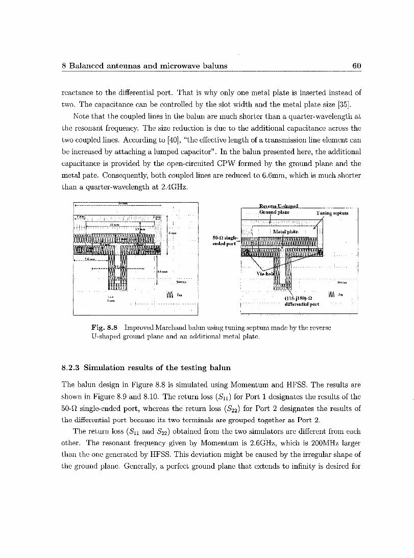
8 Balanced antennas and microwave baluns 60
reactance to the differential port. That is why only one met al plate is inserted instead of
two. The capacitance can be controlled by the slot width and the met al plate size [35].
Note that the coupled lines in the balun are much shorter than a quarter-wavelength at
the resonant frequency. The size reduction is due to the additional capacitance across the
two coupled lines. According to [40], "the effective length of a transmission line element can
be increased by attaching a lumped capacitor". In the balun presented here, the additional
capacitance is provided by the open-circuited CPW formed by the ground plane and the
metal pate. Consequently, both coupled lines are reduced to 6.6mm, which is much shorter
than a quarter-wavelength at 2.4GHz.
50-!l. single,.:..-~~œa ellded port .
EottOlD
To.
Il'U" differelltial port
Fig. 8.8 Improved Marchand balun using tuning septum made by the reverse U-shaped ground plane and an additional metal plate.
8.2.3 Simulation results of the testing balun
septum
Bottom
T,,!>
The balun design in Figure 8.8 is simulated using Momentum and HFSS. The results are
shown in Figure 8.9 and 8.10. The return loss (S11) for Port 1 designates the results of the
50-0 single-ended port, whereas the return loss (S22) for Port 2 designates the results of
the differential port because its two terminals are grouped together as Port 2.
The return loss (S11 and S22) obtained from the two simulators are different from each
other. The resonant frequency given by Momentum is 2.6GHz, which is 200MHz larger
than the one generated by HFSS. This deviation might be caused by the irregular shape of
the ground plane. Generally, a perfect ground plane that extends to infinity is desired for

8 Balanced antennas and microwave baluns 61
Momentum simulations because aH ports can be referenced to the same ground. However,
the perfect ground plane is not suit able for the balun design because slots are inserted in
between the ground plane and the additional met al plate to improve the balun performance.
In addition, when using DifferentiaI Port in Momentum, it is assumed that no ground plane
is present in the system and the two terminaIs in the DifferentiaI Port serve as ground for
each other [17] (A typical example is the simulation of the differential dipole antenna in
Section 8.1.1). In contrast, when there is no perfect ground plane in the system, a ground
reference is needed for the InternaI Port or Single Port, which is the case for the single
ended port in the balun design. Due to these conflicting requirements, errors might be
occurred during simulation because there are two separate ground references in the system.
Nevertheless, sin ce the bandwidth given by the two simulators is large enough to cover the
operating frequency of the balanced dipole antenna, this might not be a problem because
the balun is only for testing. Measurement is needed to confirm this assumption.
-5
-10
-15
iD ~ -20
"' -25
-30
-35
10_ ...... ..:
-5
~ -10
81 00-15
-20
-25
-30
1.-.. HFSS 1 -ADS
-401:-----:,7.2 ----:,:7.4 -,:7.6 -:'::1..--:-2 --::':2.2::--72.4::---:'2.=-6 --::2.7-. ----: -35 '-------'--"-----'---'----'----'-------'--'--'----' 1 U U U U 2 U U U U
Frequency (GHz) Frequency (GHz)
Fig. 8.9 Simulated return 1088 (811 and 822) for the Marchand balun of Figure 8.8.
The simulated insertion loss (812 and 821 ) for the balun is shown in Figure 8.10. A
perfect balun has a OdB insertion loss when the two ports are not coupled to each other.
Again, the insertion loss values generated by Momentum and HFSS are different from each
other. Fortunately, they are both within the acceptable limit « -2.5dB) from 2.1GHz to
3GHz, which covers the operating frequency range. This insertion-loss level is close to the
-3dB insertion loss reported in [40].

8 Balanced antennas and microwave bal uns 62
Limitations of the EM simulators
The imperfect simulation results of the testing balun show the limitations of the two EM
simulators. In Momentum, "Single Port" or "InternaI Port" with a perfect ground plane
will give the most accurate results. However, a perfect ground plane is not suit able in
many designs (including the dipole antennas we studied in this thesis). The problem will
be further complicated by the mixture of differential port and single-ended port in the
balun design. When a "DifferentiaI Port" is used in Momentum, the program assumes that
there is no ground plane in the system. In contrast, a ground reference is always needed for
"Single Port" or "InternaI Port" in Momentum. These confiicting requirements may result
in errors in the simulation results for the balun design. The same problem do es not exist
in the antenna designs of the previous chapt ers because there is no mixture of differential
port and single-ended port.
Although the ground reference problem do es not exist in HFSS, ports with complex
impedance may generate the undesired positive return loss. Since the ports are fed with
a virtual waveguide in HFSS, the results are most accurate if the ports have a purely
resistive impedance (e.g. standard 50-0 impedance). Inaccurate positive return loss might
be obtained if the resistance is lower than the reactance in the impedance setting. This
is due to the excitation of the "non-propagating" mode of the waveguide in regions far
from the operating frequency. Sinee the positive return loss creates uncertain spots in the
frequency domain, measurement is needed to characterize the real balun behavior at those
frequencies.
8.2.4 Simulation results of the testing balun with the differential antenna
Though the results given by the two EM simulators are imperfect, they still show that the
balun satisfies an the testing requirements in the operating frequency range of the antenna
(2.4GHz to 2.5GHz). Hence, the testing balun can be used as an interface between the
balanced antenna and the unbalanced port of the 2-port VNA. The next step is to attach
the "end-loaded" balanced dipole antenna of Figure 8.4 to the the balun of Figure 8.8
and examine the effects of the balun on the antenna performance (see Figure 8.11). The
simulated results are shown in Figures 8.12 and 8.13. The results of the antenna without
the balun are also shown for comparison.
After the insertion of the balun, the resonant frequency of the antenna is shifted from

8 Balanced antennas and microwave baluns 63
-2 .
1 ...... HFSS 1 -ADS
-20
-25 '------'---'------'---'------'---'-----'-----'-----,"'--------' 1 1.2 1.4 1.6 1.8 2 2.2 2.4 2.6 2.8
_20'---------'---_-'---------'--_-'------'-_---'-----'"-,------L...---,L-----' 1 U U 2 U U U U
Frequency (GHz) Frequency (GHz)
Fig. 8.10 Simu1ated insertion 10ss (812 and 821 ) for the Marchand ba1un of Figure 8.8.
2.44GHz to 2.41GHz. The return loss (S11) is below -IOdB from 2.3GHz to 2.5GHz, re
sulting in a bandwidth of 200MHz. Comparing to the 300-MHz bandwidth of the original
antenna (without the balun), the bandwidth is reduced by IOOMHz. In addition, the balun
ait ers the radiation patterns of the antenna. Although the H-plane pattern remains the
same, the null at 270 0 in the E-plane pattern is canceled when the balun is attached to the
antenna. Further comparison between the two antennas is summarized in Table 8.1.
Table 8.1 Effects of the ba1un on the antenna performance of the "endloaded" ba1anced dipole antenna.
Antenna Performance 1 Antenna without balun 1 Antenna with the testing balun
Gain 2.0dB 2.2dB Efficiency 85% 85% Bandwidth 300MHz 200MHz Resonant frequency 2.44MHz 2.41MHz
From these results, we see that testing the balanced antenna through a physical balun
only gives a rough estimate of the antenna performance. The balun affects the resonant
frequency, the bandwidth, the radiation patterns, and the gain of the antenna. Although
in most cases, these modifications do not disturb the antenna in the operating frequency
range, the antenna performance becomes highly dependent on the balun characteristics,
which is undesirable. Therefore, using a physical balun for differential measurement can be

8 Balanced antennas and microwave baluns 64
considered as a Pass/Fail test for the preliminary antenna design. Once a successful model
is fabricated, more accurate measurement using 4-port VNA or the calculated mixed-mode
S-parameter technique are needed to accurately characterize the balanced antenna. Due
to the complexity of the differential testing, the differential dipole antenna is less popular
than its single-ended counterpart with the integrated balun.
50-il singleended port
buiU tes tin g
Fig. 8.11 "End-loaded" differential dipole antenna of Figure 8.4 is attached to the balun of Figure 8.8 before testing.
8.3 Improving the balun performance at high frequency
As mentioned in the previous sections, the RF port of the transceiver is differential and
requires a balun if an unbalanced antenna is used. Employing a balanced antenna can help
avoid the balun but also raises the difficulty of testing. In fact, many existing antennas are
unbalanced and still need the bal uns to operate correctly in a differential system. One of
the merits of the testing balun design is that the same design methodology can be adopted
to design a microwave balun that improves the performance of the unbalanced antenna
system at high frequency. Although the lumped-component balun network provided by
the transceiver data sheet can still be used in the low-GHz range, as frequency increases,
these components have size comparable to the free-space wavelength and no longer behave
as perfect RLC components. Thus, balun design using lumped (or dis crete ) components
is not suit able for high-frequency applications. In those cases, baluns based on microwave
components, microstrip or copI anar couplers are more appropriate [6, 41]. In this section, we
discuss the possibility of replacing the existing balun using microstrip lines and microwave
components.

8 Balanced antennas and microwave baluns
1.2 1.4 1.6 1.8 2 2.2 2.4 2.6 2.8 3 Frequency (GHz)
Fig. 8.12 Simulated return loss (S11) of the 'end-Ioaded" balanced dipole antenna with the balun of Figure 8.11.
Anteuull ttitbout baluu
+ Antenna \\itll baltm o
270 1---1---+f-+--+~Ijo-*---1E:+--fIoo-t---I---I
210 1!iO
180
90
- Al1telUlll witllollt bahm
+ Antt'IlUll with Imhm o
270 t---+++-f--t---+-*:-t--t---+-..-t----1
180
Fig. 8.13 Simula.ted E-plane and II-plane radiation patterns for the "endloaded" balanced dipole antenna with the testing balun (Figure 8.11). Patterns for the same antenna without balun (Figure 8.4) are also shown for cornparison
65
90

8 Balanced antennas and microwave baluns 66
8.3.1 Design configuration of the microwave balun
The design concept of the microwave balun is similar to the testing balun. The new balun
still has a singled-ended port and a differential port. The only difference is that the single
end port is connected to an unbalanced antenna, whereas the differential port is connected
to the RF port of the transceiver. The single-ended port has the standard 50-D impedance.
The differentiaI-port impedance should be equal to the ideal differentialload (115+j180 D)
because the balun becomes the load for the transceiver. Since the reactance of this load is
inductive, the testing balun of Figure 8.8 cannot be used because it has capacitive tuning
septum. Nevertheless, the design methodology is the same as shown in the last section
and the balun is still based on the Marchand balun. The layout of the microwave balun is
shown in Figure 8.14.
50-0 siuglt-
Diffel'eutiai RF-I)OIt + TxiR.\: llort (bia~'iug)
Fig. 8.14 Layout of the microwave balun based on the folded Marchand baluIl.
The configuration in Figure 8.14 is a folded Marchand balun, which is the same as the
J-shaped balun in Chapter 3. The theory can be found in Section 3.1.1. The top layer
(in darker color) contains the microstrip line inductor, the triangular "fan-Ioad" capacitor
(which will be discussed later), and the J-shaped microstrip line. The latter has one end
open-circuited (forming the open-circuited stub) and the other end connected to the 50-0

8 Balanced antennas and microwave bal uns 67
single-ended port. The bottom layer (in light color) contains the copi anar strips and the
differential port. The coplanar strips are about quarter-wavelength long. One of its ends is
shorted together to form the short-circuited stub. The other end extends into two narrow
lines to create the high resistance (115 D) for the differential port. In microwave engineering,
inductors can be realized using high-impedance microstrip lines or spiral conductors [35].
Applying the same concept, the required inductance (j180 D) can be obtained by adding
a narrow microstrip line across the two terminaIs of the differential port. To achieve the
high inductance, the width of the micros trip line is made narrow « 2mm) and the ground
below the line is removed.
For biasing purposes, the microstrip-line inductor is also connected to the TX/RX port
(which is in-between the two terminaIs of the RF port in Figure 8.14). Besides the inductor,
a shunt biasing capacitor is also connected to the same port. Together with the inductor,
the shunt capacitor provide the DC-bias for the low-noise amplifier and power amplifier
(LNA and PA) input/output in the transceiver [28]. This biasing capacitor is formed by a
triangular "fan-load" capacitor (as known as a microstrip radial stub) in Figure 8.14.
8.3.2 Simulation results for the microwave balun
The design in Figure 8.14 is simulated using Momentum and HFSS. The setup is the same
as the testing balun in Section 8.2.3. The results are shown in Figures 8.15 and 8.16. The
return loss (8n ) for Port 1 designates the results of the 50-D single-ended port, whereas
the return loss (822 ) for Port 2 designates the results of the differential port because its
two terminaIs are grouped together as Port 2.
Similar to the testing balun, the results given by Momentum and HFSS are different
from each other. Although the resonant frequencies generated by the two simulators are
close to each other (rv2.45GHz), the return loss (822 ) for Port 2 and the insertion loss (821
and 812 ) given by Momentum are 5dB higher than the ones given by HFSS. As explained
in Section 8.2.3, these deviations may be due to the imperfect ground plane, the mixture of
"DifferentiaI Port" and "InternaI Port" in Momentum, and the complex port impedance in
HFSS. Measurement is needed to characterize the real performance of the balun. Nervethe
less, the return loss for both ports (8n and 822 ) is below -15dB and the insertion loss (821
and 812 ) is less than -4dB in the operating frequency range (2.4 to 2.5GHz) of the Zigbee
transceiver, which are still within the acceptable range.

8 Balanced antennas and microwave baluns
-4
-6
iD -8
" <ii -10
-12
-14
-16
-5
l'~ HFSS 1 -+- ADS
Fig. 8.15 Simu1ated retum 10ss (811 and 822) for the microwave ba1un of Figure 8.14.
1 HFSS 1 -t- ADS
I-HFssl -+- ADS
-5
1.2 1.4 1.6 1.8 2 2.2 2.4 2.6 2.8 1.2 1.4 1.6 1.8 2 2.2 2.4 2.6 Fraquency (GHz) Frequency (GHz)
Fig. 8.16 Simu1ated insertion 1088 (812 and 821) for the rnicrowave ba1un of Figure 8.14.
68

8 Balanced antennas and microwave bal uns 69 -------------
8.4 Simulation results of the microwave balun with the
unbalanced antenna
Though the simulation results given by the two simulators are different from each other,
both of them show that the balun satisfies all the requirements of the Zigbee transceiver
in the operating frequency range (2.4GHz to 2.5GHz). Thus, the microwave balun can still
be used to replace the lumped-component balun. The next step is to attach a single-ended
(i.e unbalanced) antenna to the single-ended port the the microwave balun of Figure 8.14
and examine the effects of the balun on the antenna performance (see Figure 8.17). The
differential port of the balun will be connected to the RF port of the transceiver in the
complete setup.
The layout of the microwave balun with the unbalanced antenna is shown in Figure 8.17.
The unbalanced "end-Ioaded" dipole antenna (Figure 4.1) is selected because it is also used
for the PCB integration with the Zigbee transceiver in Chapter 7. In theory, any unbalanced
antenna can be used with the microwave balun. The design in Figure 8.17 is simulated
using Momentum and HFSS. The setup is almost the same as the balun simulation in
Section 8.2.3, except that only the differential port is present because the single-ended port
is connected to the input of the "end-loaded" unbalanced dipole antenna. The simulated
results are shown in Figures 8.18 and 8.19.
Similar to the results of the testing balun and the microwave balun, the return loss given
by Momentum and HFSS are different from each other. The major discrepancy is found
in regions far from the operating frequency range (i.e. f< 2.2GHz and f>2.6GHz). From
2.2GHz to 2.6GHz, the two curves have similar behavior. As explained in Section 8.2.3, the
difference is mainly due to the imperfect ground plane in Momentum and the complex port
impedance in HFSS. Neverthele~s, the results in the operating range (2.4GHz to 2.5GHz)
are still acceptable for the Zigbee application. The return loss is less than -10dB from
2.3GHz to 2.7GHz, resulting in a 400-MHz bandwidth. The radiation patterns are still
roughly omnidirectional. The presence of the microwave balun increases the front-to-end
(dipole arms to microwave balun) ratio to O.84dB, which is still acceptable when comparing
to the O.57dB front-to-end ratio of the original "end-Ioaded" dipole antenna of Figure 4.l.
Further comparison between the "end-loaded" dipole antenna alone and the same antenna
with the microwave balun is summarized in Table 8.2.
The results in Table 8.2 show that the the microwave balun degrades slightly the an-

8 Balanced antennas and rnicrowave baluns
l\lltl'Owan BIIlIll\
{Tub, mlcNI "ell,ll<m,1e11" dip.o mlttlUHl
Fig. 8.17 Layont of the unbalanced "end-loaded" dipole antenna with the mic:rowave balnn.
5
0.,.._-..
-10
-15
âl u ;:: -20
èiï
-40
_45L-__ ~ ____ -L ____ ~ ____ L-__ ~ ____ -L ____ -L __ ~~ ____ L-__ ~
1 1.2 1.4 1.6 1.8 2 2.2 2.4 2.6 2.8 3 Frequency (GHz)
Fig. 8.18 Simlllated return 1088 (S11) of the unbalanced "end-loaded" dipole antenna with the mic:rowave balun of Figure 8.17.
70

8 Balanced antennas and microwave baluns
-- Towards the dipole arms o
330 30
270 f---_t__f__-+~i""'-+_*_+E::t-+___t__f_____1 90 270 I-----HI--I---+---j-*--l--!--++-+_-I 90
180 180
Fig. 8.19 Simulated E-plalle and II-plane radiation patterns for the unbalanced "end-loaded" dipole antenna with the microwave balun of Figure 8.17.
Table 8.2 Comparison between the "end-Ioaded" dipole antenna (Figure 4.1) and the same antenna with the microwave balun (Figure 8.17).
Antenna Performance "End-Ioaded" dipole antenna "End-loaded" dipole antenna without the microwave balun with the microwave bahm
(Figure 4.1) (Figure 8.17)
Peak Gain 2.85dB 2.42dB Efficiency 99.4% 87.9% Cross-polarization level -25.35dB -17.50dB Bandwidth 250MIIz 400l\"IIIz
71

8 Balanced antennas and microwave baluns 72
tenna performance, but overall, the resulting antenna is still acceptable for the Zigbee
application. Most importantly, since the microwave balun is composed of transmission
lines without lumped components, it is readily functional in high-frequency applications.
Replacing the lumped-component balun with the microwave balun can also reduce the fab
rication co st of the device. Although the size of the microwave balun is comparable to the
lumped-component balun at 2.4GHz, as the operating frequency increases, the size of the
transmission lines will be decreased, resulting in a more compact microwave balun design.

73
Chapter 9
Conclusion
In this thesis, we studied popular printed dipole antennas. The major disadvantage of these
antennas is their relatively large size. Miniaturization technique inspired by the capacitor
plate antenna can reduce the antenna size by 60%. The finished design is compact and
flexible in frequency tuning. The lost bandwidth resulting from miniaturization can be
recovered by using tapered arms and parasitic elements around the edges of the dipole
arms. A combinat ion of both techniques results in a 500-MHz bandwidth. Like most
omnidirectional antennas, our designs have two nulls along the dipole arms on the E-plane
radiation pattern. Using bent arms and asymmetrical copI anar strip can cancel these nulls.
To prove the functionality of the proposed antenna designs in future wireless networks,
one of them was integrated with an IEEE 802.15.4 (Zigbee) transceiver on the same PCB.
The design methodology involving the integration and related issues were presented. Care
fuI selection of dielectric substrate material and antenna type facilitates the design pro cess
and reduces the number of board returns. Experiments showed good agreement between
the simulation model and the real integrated antenna.
To improve the antenna performance, a complete differential RF front-end with a bal
anced antenna was studied. The major obstacle relies on the difficulties of the differential
measurement, which was demonstrated by the imperfect results of the testing bal un. Fi
nally, to improve the antenna performance at high frequency, the lumped-component balun
was replaced by a new microwave balun composed of transmission lines and microwave com
ponents. Due to the limitations of the EM simulators, measurement is needed to confirm
the simulation results in the future.
2005/07/26

9 Conclusion 74
Since aH antennas proposed here were designed for the unlicensed 2.4-GHz ISM band,
future work includes modifying the antenna designs for other frequencies. The possibility of
building the antennas on inexpensive dielectric substrate (e.g FR4 material) holds potential
for future investigations. Most importantly, the design methodology proposed in this thesis
is universal and can be applied in other printed antenna designs. Experiments with other
antenna types are needed to confirm this assumption.

75
Appendix A
Basic Transmission Line Theory
A.l Equations for the characteristic impedance of the microstrip
Hne
{
...QQ...ln (8d + W) z- Fe W 4d o - 12011"
Fe[W/d+1.393+0.6671n(W/d+1.444)]
for W Id ::; 1
for W/d ~ 1 (A.1)
Notice that W is the width of the microstrip line and d is the thickness of the dielectic
substrate. However, Eq.(A.1) is valid only if the ground plane is at least 3 times wider
than the width of the microstrip line.
A.2 Theory behind the coupled Hne: Even-mode and Odd-mode
propagation
A coupled line consists of two parallel transmission lines placed in close proximity on
top of a dielectric substrate. Due to the coupling of the electromagnetic field between the
parallellines, the coupled line can support two propagation modes. Even-mode propagation
implies two signaIs of the same amplitude and zero phase difference passing through the
coupled line. In contrast, odd-mode operation denotes the propagation of two signaIs of the
same amplitude but 180 0 phase difference. Due to the inhomogeneous dielectric medium
(air + substrate), the two modes have different effective dielectric constants and phase
velocities that degrade the performance of the cou pIed lines [35]. When operating different
2005/07/26

A Basic Transmission Line Theory 76
modes, the effective capacitance between the two transmission lin es and the ground plane
is different and contribute to two impedances: even-mode and odd-mode impedances (ZOe
and Zoo). The characteristic impedance of the coupled line is dependent on ZOe and Zoo;
their relationship is summarized in Equation A.2 [35].
ZS2 = JZOe· Zoo (A.2)
According to [7], the characteristic impedance of the coupled line can be determined
from the propagation velo city on the line (v) and the effective capacitance between the
transmission lines. The even-mode and the odd-mode impedance ZOe and Zoo can be
obtained using Equations A.3 and A.4, respectively. Note that the effective capacitances
Ce and Ce for different modes are different from each other. The equivalent capacitive
network for a coupled li ne is shown in Figure A.l. When operating in the even mode, no
current fiows between the two transmission lines and C12 is open-circuited. The effective
capacitance Ce is given by Equation A.5. The resulting network for even-mode is depicted
in Figure A.2.
When operating in the odd mode, the two transmission lines are cou pIed to each other,
resulting in a finite C12 • There is also a virtual ground in between the two lines. The
equivalent network for the odd mode is shown in Figure A.3. The effective capacitance Co
is given by Equation A.6.
Z _ {g_ y'LCe __ 1_
Oe - - -Ce Ce vCe
(A.3)
(A.4)
(A.5)
(A.6)

A Basic Transmission Line Theory
uu Fig. A.l The coupled-line model and its equivalent capacitive network. C11 and C22 are the capacitance between each line and the ground. C12 is the mutual capacitance between the two lines (Figure taken from [7]).
CIl 1-- --le T'------<~p---T 22
Fig. A.2 Even-mode excitation on a coupled line and its resulting equivalent capacitance networks (Figure taken from [7]).
+'/1/ / I-v
\fLk[ jj (l~t\
,''''~'''~'''''''''', 1 1 E-wall
Fig. A.3 Odd-mode excitation on a coupled line and its resulting equivalent capacitance networks (Figure taken from [7]).
77

78
References
[1] D. Edward and D. Rees, "A broadband printed di pole with integrated balun," Microwave Journal, pp. 339-344, May 1987.
[2] W. K. Roberts, "A new wide band balun," Proceedings of the IRE, vol. 45, pp. 1628-1631, Dec. 1957.
[3] G. Oltman, "The compensated balun," IEEE Trans. Microwave Theory Tech., vol. 14, pp. 1628-1631, Mar. 1966.
[4] H.-R. Chuang and L.-C. Kuo, "3-D FDTD design analysis of a 2.4-ghz polarizationdiversity printed dipole antenna with integrated balun and polarization-switching circuit for WLAN and wireless communication applications," IEEE Trans. Microwave Theory Tech., vol. 51, no. 2, Feb. 2003.
[5] M. Scott, "A printed dipole for wide-scanning array application," in 2001 Eleventh International Conference on Antennas and Propagation) (IEE Conf. Publ. No. 480), vol. 1, Apr. 17-20, 2001, pp. 37-40.
[6] E. Valletta, L. de Vreede, and J. Burghartz, "Design of planar marchand balun for mmic applications," in Proceedings of SAPE 2002, Veldhoven, Netherlands, Nov. 27-28, 2002. [Online]. Available: http://www.stw.nl/safe/proc-2002/valletta.pdf
[7] D. M. Pozar, Microwave Engineering. Addison-Wesley Publishing Company, Inc, 1990.
[8] W. L. Stutzman and G. A. Thiele, Antenna Theory and Design, 2nd ed. Wiley, 1997.
[9] D. M. Pozar, "Microstrip antennas," Proceedings of the IEEE, vol. 80, pp. 79-91, Jan. 1992.
[10] C. Soras, M. Karaboikis, G. Tsachtsiris, and V. Mikios, "Analysis and design of an inverted-F antenna printed on a PCMCIA card for the 2.4GHz ISM card," IEEE Antennas Propagat. Mag., vol. 44, pp. 37-44, Feb. 2002.

References 79
[1l] Y. Coulibaly, T. A. Denidni, L. Talbi, and A. R. Sebak, "A new single layer broadband cpw fed-printed monopole antenna for wireless applications," in 2004 Canadian Conference on Electrical and Computer Engineering, vol. 3, May 2-5,2004, pp. 1541-1544.
[12] K. Rambabu, M. Alam, J. Bornernann, and M. A. Stuchly, "Compact wideband dualpolarized microstrip patch antenna," in 2004 IEEE Antennas and Propagation Society Symposium, vol. 2, June 20-25, 2004, pp. 1955-1958.
[13] S. Targonski and D. M. Pozar, "Design of wideband circularly polarized aperturecoupled micros trip antennas," IEEE Trans. Antennas Propagat., vol. 41, pp. 214-220, Feb. 1993.
[14] B. Lee and T. Yang, "A novel wide bandwidth cp stacked microstrip patch antenna," in 2000 IEEE Antennas and Propagation Society International Symposium, vol. 2, July 16-21, 2000, pp. 1004-1007.
[15] N. Michishita and H. Arai, "FDTD analysis of printed monopole antenna," in 2001 Eleventh International Conference on Antennas and Propagation, (IEE Conf. Publ. No. 480), vol. 2, ApL 17-20,2001, pp. 728-731.
[16] Agilent, "Multiport and balanced device measurement application notes series - concept in balanced device measurements application note 1373-2," Agilent Technologies," Application note, 2002.
[17] --, "Advanced design system 2003a documentation," Agilent Technologies," Product Documentation, 2003.
[18] Ansoft HFSS. [Online]. Available: http:j jwww.ansoft.comjproductsjhfjhfssj
[19] M. Gimersky and J. Bornemann, "A modified method-of-moments technique for the full-wave analysis of imperfect conductors on lossy and finite-extent substrates," in Microwave Symposium Digest, 1996, IEEE MTT-S International, vol. 2, June 17-21, 1996, pp. 715-718.
[20] W. H. Haydl, "On the use of vias in conductor-backed coplanar circuits," IEEE Trans. Microwave Theory Tech., vol. 50, pp. 1571-1577, June 2002.
[21] D. M. Pozar and D. H. Schaubert, Microstrip antennas: The analysis of design of microstrip antennas and arrays. Wiley-IEEE Press, 1995.
[22] M. Abdel-Aziz, H. Ghali, H. Ragaie, H. Haddara, E. Larique, B. Guillon, and P. Pons, "Design, implementation and measurement of 26.6 ghz patch antenna using me ms technology," in 2003 IEEE International Symposium on Antennas and Propagation, vol. 1, June 22-27, 2003, pp. 399-402.

References 80
[23] R. Chu, A. Wang, and K. Lee, "Analysis of wideband tapered element phased array antennas," in 1994 Antennas and Propagation Society International Symposium, APS. Digest., vol. 1, June 20-24, 1994, pp. 498-50l.
[24] S.-G. Mao, C.-H. Chan, C.-I. Hsu, and D.-C. Chang, "A series-fed printed-bowtie antenna with broadband characteristics and end-fire radiation," in 2001 Asia-Pacific Microwave Conference, APMC'2001, vol. 2, Dec. 3-6, 2001, pp. 926-929.
[25] J. Lee and S. Livingston, "Wide band bunny-ear radiating element," in 1993 Antennas and Propagation Society International Symposium, (AP-S). Digest, vol. 3, JunejJuly 1993, pp. 1604-1607.
[26] K. Chang, H. Kim, K. S. Hwang, S. H. Sim, S. J. Yoon, and Y. J. Yoon, "A wideband dual frequency printed dipole antenna using a parasitic element," in 2003 IEEE Topical Conference on Wireless Communication Technology, Oct. 15-17, 2003, pp. 346-347.
[27] Freescale, "Compact, integrated antennas: Designs and applications for the mc13191 and mc13192 (an2731 rev. 1.2)," Freescale Semiconductor," Application note, 2004.
[28] Chipcon, "Smart RF CC2420 preliminary datasheet (rev 1.2)," Chipcon AS, Gaustadalléen 21 NO-0349, Oslo, NORWAY, Datasheet, 2004.
[29] X. Ye, D. M. Hockanson, M. Li, Y. Ren, W. Cui, J. L. Drewniak, and R. E. DuBroff, "EMI Mitigation with multilayer power-bus stacks and via stitching of reference planes," IEEE Trans. Electromagn. Compat., vol. 43, pp. 538-548, Nov. 200l.
[30] F. Xiao, K. Murano, and Y. Kami, "The use of via holes for controlling the crosstalk of non-parallel microstrip lines on PCBs," in 2002 IEEE International Symposium on Electromagnetic Compatibility, vol. 2, Aug. 19-23, 2002, pp. 633-638.
[31] D. D. Henkes, "Ordinary vector network analyzers get differential port measurement capability," High Frequency Electronics, vol. 2, no. 6, pp. 54-62, Nov. 2003.
[32] N. Marchand, "Transmission line conversion transformers," Electronics, vol. 17, p. 142, Dec. 1944.
[3:3] Y. J. Yoon, Y. Lu, R. C. Frye, M. Y. Lau, P. R. Smith, L. Ahlquist, and D. P. Kossives, "Design and characterization of multilayer spiral transmission-line baluns," IEEE Trans. Microwave TheoTy Tech., vol. 47, pp. 1841-1847, Sept. 1999.
[34] M. Tsai, "A new compact wideband balun," in 1993 IEEE Microwave and MillimeterWave Monolithic Circuits Symposium, 1993. Digest of Papers, June 14-15, 1993, pp. 123-125.

References 81
[35] K. Gupta, R. Garg, I. Bahl, and P. Bhartia, Microstrip Lines and Slotlines, 2nd ed. 685 Canton Street, Norwood, MA 02062: Artecg House Publishers, 1996.
[36] Z. Zhang, Y.-X. Guo, L. C. Ong, and M. Y. W. Chia, "Improved planar marchand balun using a patterned ground plane," International Journal of RF and Microwave Computer-Aided Engineering, vol. 15, pp. 307-316, Mar. 2005.
[~H] K. S. Ang, Y. C. Leong, and C. H. Lee, "Multisection impedance-transforming coupledli ne baluns," IEEE Trans. Microwave Theory Tech., vol. 51, pp. 536-541, Feb. 2003.
[38] M. Shimozawa, K. Itoh, Y. Sasaki, y. I. Hazime Kawano, and O. Ishida, "A parallel connected marchand balun using spiral shaped equal length coupled lines," in 1999 IEEE International Microwave Symposium Digest, IEEE MTT-S, vol. 4, June 13-19, 1999, pp. 1737-1740.
[39] A. M. Pavio and A. Kikel, "A monolithic or hybrid broadband compensated balun," in 1990 IEEE International Microwave Symposium Digest, IEEE MTT-S, May 8-10, 1990, pp. 483-486.
[40] S. Ojha, G. R. Branner, and B. P. Kumar, "A miniaturized lumped-distributed balun for modern wireless communication systems," in 1996 IEEE 39th Midwest symposium on Circuits and Systems, vol. 3, Aug. 18-21, 1996, p. 13471350.
[41] T.-H. Chen, K. Chang, S. Bui, H. Wang, G. Dow, L. Liu, T. Lin, and W. Titus, "Broadband monolithic passive baluns and mono lit hic double-balanced mixer," IEEE Trans. Microwave Theory Tech., vol. 39, pp. 1980-1986, Dec. 1991.