presentation of the national institute for research and physico-chemical analysis inrap pr. najoua...
TRANSCRIPT
PRESENTATION OF THE NATIONAL
INSTITUTE FOR RESEARCH AND
PHYSICO-CHEMICAL ANALYSIS
INRAP
PR. NAJOUA KAMOUN TURKIGENERAL DIRECTOR
Institut National de Recherche et d’Analyse Physicochimique
e-age December 12-13/2013
PR NAJOUA KAMOUN TURKI GENERAL DIRECTOR OF INRAP
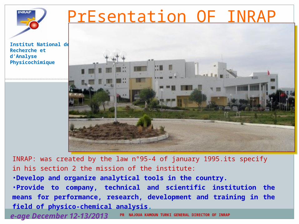
PrEsentation OF INRAP
Institut National de Recherche et d’Analyse Physicochimique
INRAP: was created by the law n°95-4 of january 1995.its specify in his section 2 the mission of the institute:•Develop and organize analytical tools in the country. •Provide to company, technical and scientific institution the means for performance, research, development and training in the field of physico-chemical analysis.
e-age December 12-13/2013

• A documentation center in terms of physico-chemical analysis.
•A technical service center: maintain and repair scientific equipement
used by INRAP,assistance to other agencies, implementation of specific
arrangements.
•An institute of research and development
•A training center
INRAP : was designed to be
INRAP constitutive
Analysis Researche
DocumentationMaintenanceTraining
e-age December 12-13/2013
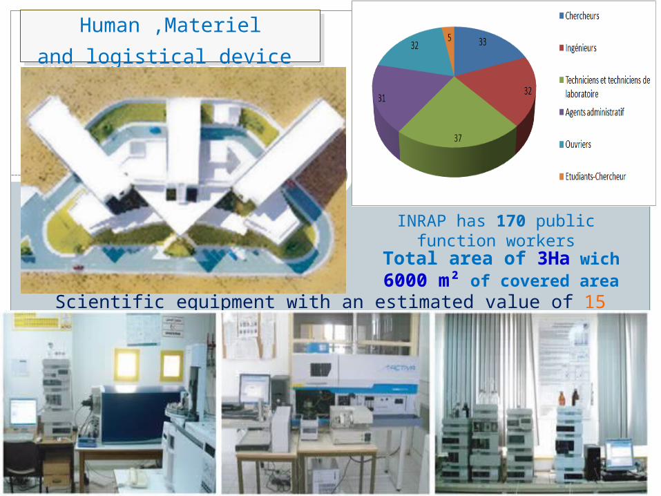
Human ,Materiel
and logistical device
Human ,Materiel
and logistical device
Scientific equipment with an estimated value of 15 MD
INRAP has 170 public function workers
Total area of 3Ha wich 6000 m² of covered area
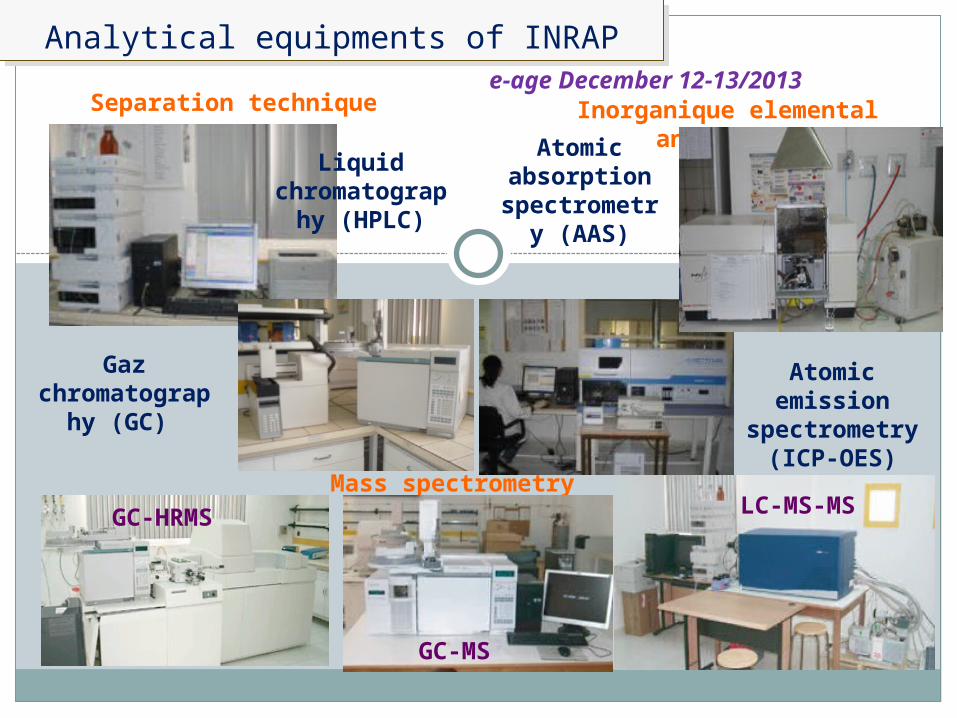
Analytical equipments of INRAPAnalytical equipments of INRAP
Separation technique
Liquid chromatography
(HPLC)
Gaz chromatography
(GC)
Inorganique elemental analysis
Atomic absorption
spectrometry (AAS)
Atomic emission spectrometry
(ICP-OES)
Mass spectrometryGC-HRMS
GC-MS
LC-MS-MS
e-age December 12-13/2013

Analytical equipments of
INRAP
Analytical equipments of
INRAPInfrared Fourrier transform
environnemental scaning electron microscopy
UV-Visible spectroscopy X fluoressence
Thermal analysis ATD ATG DSC
e-age December 12-13/2013
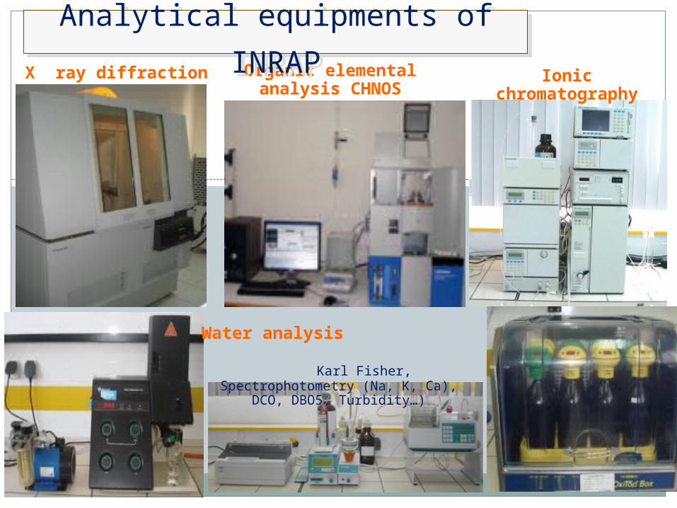
X ray diffraction Organic elemental analysis CHNOS
Ionic chromatography
Water analysis Karl Fisher, Spectrophotometry (Na, K, Ca), DCO,
DBO5, Turbidity…)
Analytical equipments of
INRAP
Analytical equipments of
INRAP

GC-MS-MS
LC-MS-MS
NMR 500 MHz
Analytical equipments of
INRAP
Analytical equipments of
INRAP
e-age December 12-
13/2013

P1 Watch Normative
P2 MétrologyMétrology
Active contribution to the adoption of international standards and
adapt to national needs
- Establishing a connection string pH measurement and a
primary reference bench pH measurement.
- Certification of buffer solution
P3 Tools and methods of analysisTools and methods of analysis
LMTA: Laboratory of Analytical and technical LMTA: Laboratory of Analytical and technical methodmethod Research projectResearch project
e-age December 12-13/2013
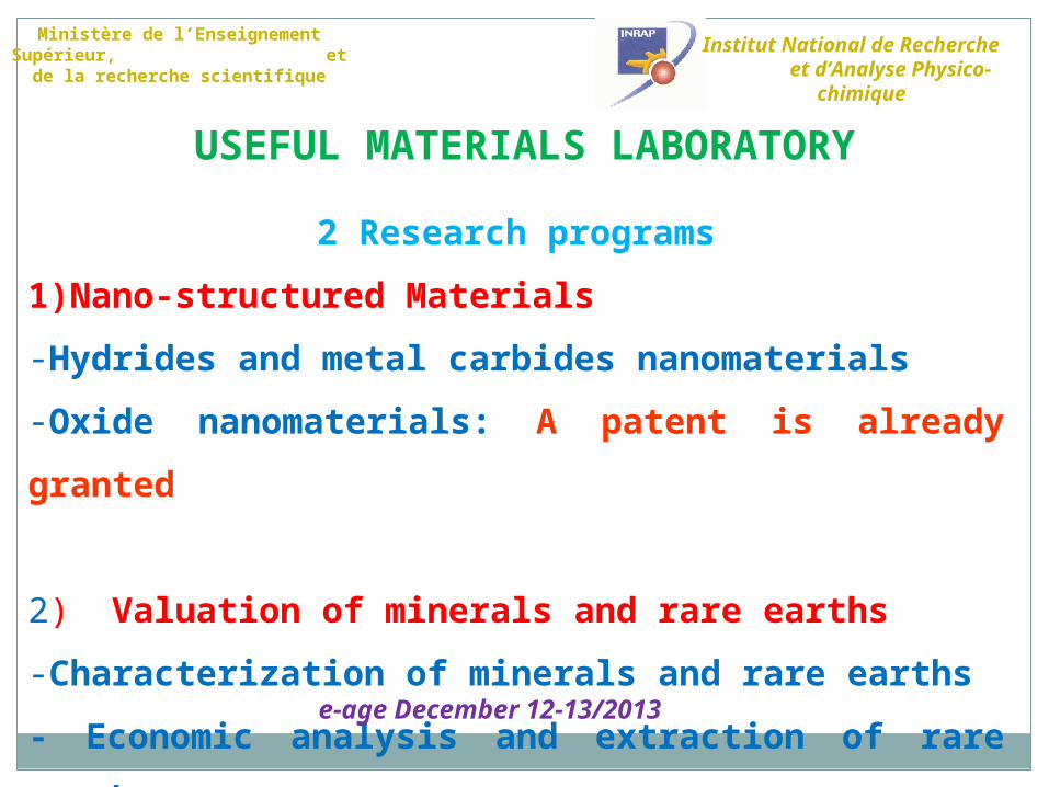
USEFUL MATERIALS LABORATORY
Ministère de l’Enseignement Supérieur, et de la
recherche scientifique
Institut National de Recherche et
d’Analyse Physico-chimique
2 Research programs
1)Nano-structured Materials
-Hydrides and metal carbides nanomaterials
-Oxide nanomaterials: A patent is already
granted
2) Valuation of minerals and rare earths
-Characterization of minerals and rare earths
- Economic analysis and extraction of rare earths e-age December 12-13/2013
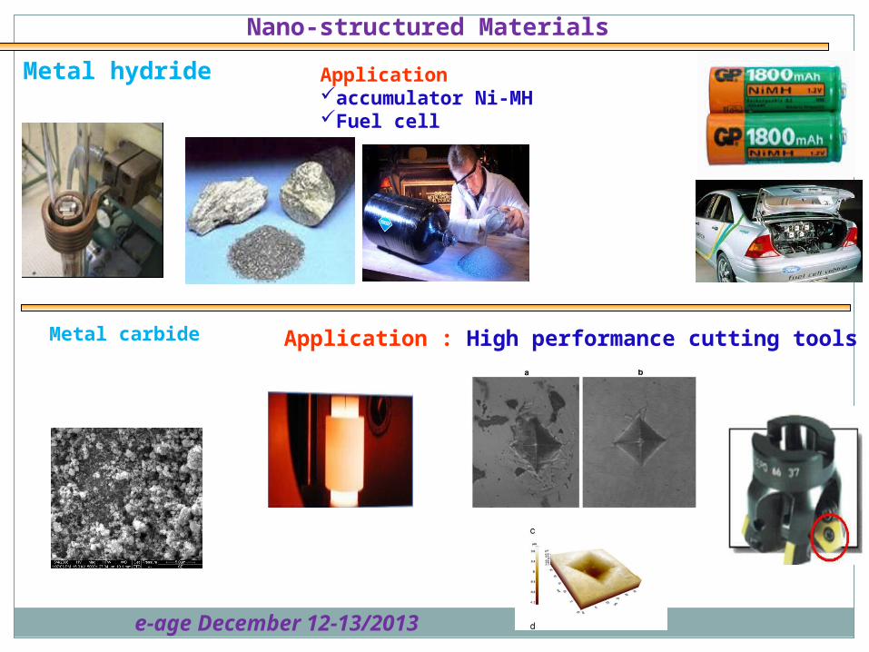
Nano-structured Materials
Applicationaccumulator Ni-MHFuel cell
Metal hydride
Metal carbide Application : High performance cutting tools
e-age December 12-13/2013
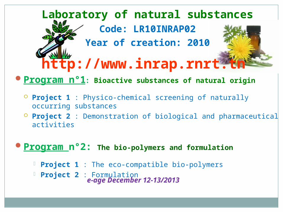
Program n°1: Bioactive substances of natural origin
Project 1 : Physico-chemical screening of naturally occurring substances
Project 2 : Demonstration of biological and pharmaceutical activities
Program n°2: The bio-polymers and formulation
Project 1 : The eco-compatible bio-polymers Project 2 : Formulation
Laboratory of natural substancesCode: LR10INRAP02
Year of creation: 2010
e-age December 12-13/2013
http://www.inrap.rnrt.tn
Synthesis and characterzation of low cost nanomaterials Synthesis and characterzation of low cost nanomaterials
used in photovoltaic devicesused in photovoltaic devices
Pr N. Kamoun Turki Director of Physics Condensed Matter
e-age December 12-13/2013

Geothermal
The waterfalls
The wind
Plant growth
Photovoltaic solar energy
Introduction: Renewable energies
14
e-age
December 12-13/2013

15
CBD: In2S3, ZnS, PbS, SnS, Cu2S : 5 Cot. Th,
2 CMCU: 03-09; AUF 2011-2012
Reagents and preparation of solution
Growth
mode
Atom-by-atom
Aglomeration clusters
Combinaison mécanisms
Deposition solution
Water bathThermometer
Agitator magnetic heating
Substrat
Nature of substrat+
Experimental Conditions
e-age December 12-13/2013

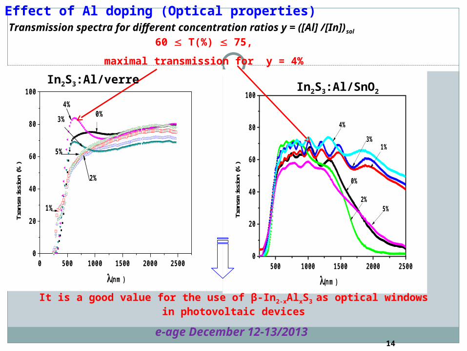
Effect of aluminum doping on the physical properties of thin films In2S3
16
e-age December 12-13/2013
500 1000 1500 2000 25000
20
40
60
80
100
Tran
smiss
ion
(%)
(nm)
0%
4%
3%1%
5%2%
Effect of Al doping (Optical properties)
14
Transmission spectra for different concentration ratios y = ([Al] /[In])sol
60 T(%) 75,
maximal transmission for y = 4%
It is a good value for the use of β-In2-xAlxS3 as optical windows in photovoltaic devices
0 500 1000 1500 2000 25000
20
40
60
80
100
Tran
smis
sion
(%)
(nm)
4%0%
1%
5%
2%
3%
In2S3:Al/verreIn2S3:Al/SnO2
e-age December 12-13/2013

Effect of tin doping on the physical properties of thin films In2S3
18
e-age December 12-13/2013
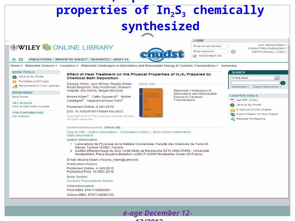
Influence of heat treatment on structural, optical and electrical properties of In2S3 chemically synthesized
19
e-age
December 12-13/2013
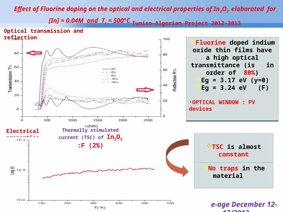
Effect of Fluorine doping on the optical and electrical properties of In2O3 elaborated for [In] =
0.04M and Ts = 500°C Tuniso-Algerian Project 2012-2013
Optical transmission and reflection
Fluorine doped indium oxide thin films have a high optical transmittance (is in order of
80%)Eg = 3.17 eV (y=0)Eg = 3.24 eV (F)
•OPTICAL WINDOW : PV devices
Fluorine doped indium oxide thin films have a high optical transmittance (is in order of
80%)Eg = 3.17 eV (y=0)Eg = 3.24 eV (F)
•OPTICAL WINDOW : PV devices
Electrical properties Thermally stimulated current
(TSC) of In2O3 :F (2%)TSC is almost constantTSC is almost constant
No traps in the material No traps in the material
e-age
December 12-13/2013
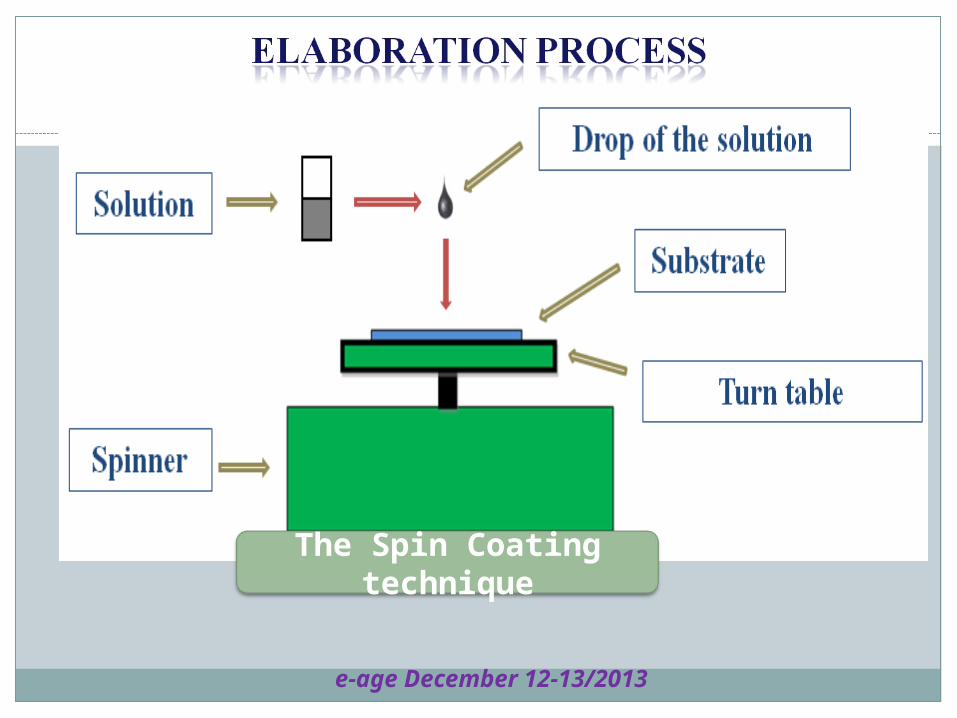
The Spin Coating technique
e-age December 12-13/2013
0 500 1000 1500 2000 2500
20
40
60
80
100
R (%)
T (%)
C = 1 g/l C = 2 g/l C = 3 g/l
0 500 1000 1500 2000 2500
20
40
60
80
R (%)
C = 1 g/l C = 2 g/l C = 3 g/l
T (%)
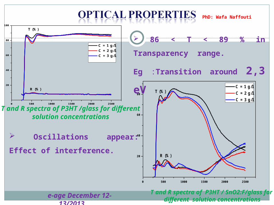
Oscillations appear: Effect of
interference.
86 < T < 89 % in Transparency
range.
Eg :Transition around 2,3 eV
T and R spectra of P3HT / SnO2:F/glass for different solution concentrations
T and R spectra of P3HT /glass for different solution concentrations
PhD: Wafa Naffouti
e-age
December 12-13/2013

EEFECT OF Ga INCORPORATION ON
PHYSICAL PROPERTIES OF CuInS2 THIN FILMS SUNTHESIZED BY CHEMICAL SPRAY
PYROLYSIS
PhD Mejda Ajili
23
e-age
December 12-13/2013

24
Chemical Spray pyrolysis
a nozzle fixed on a one-dimentional moving support allowing it to pulverize the whole isothermal zone containing the cleaned substrates placed on to heated system. The nitrogen was used as a carrier gas that serves to the pulverization of fine droplets of aqueous solution.
e-age December 12-13/2013
25
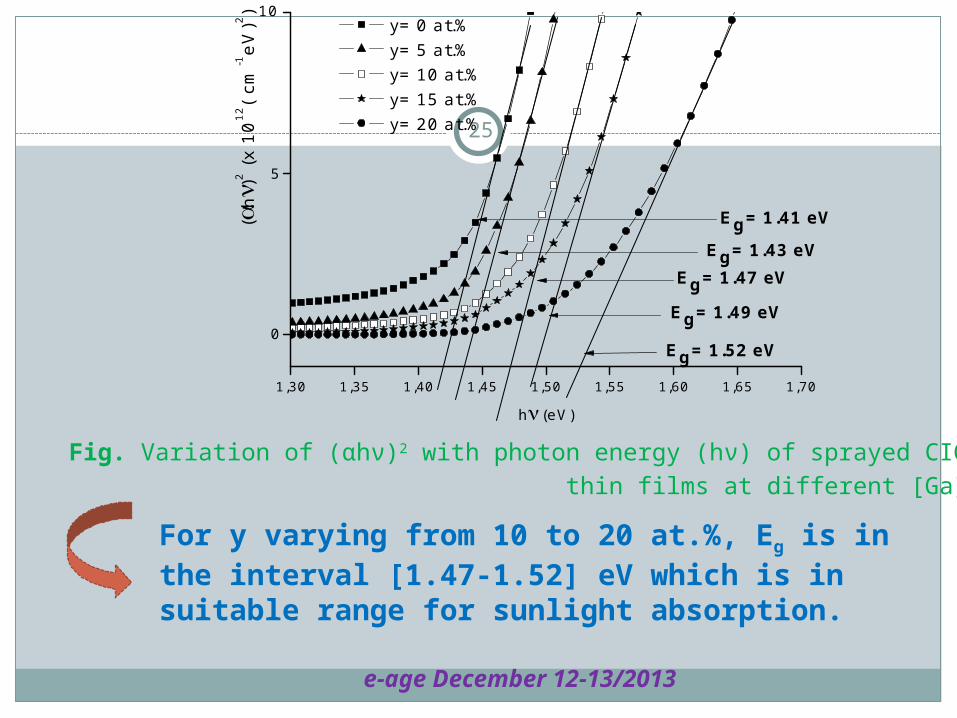
1,30 1,35 1,40 1,45 1,50 1,55 1,60 1,65 1,70
y= 0 at.% y= 5 at.% y= 10 at.% y= 15 at.% y= 20 at.%
Eg= 1.41 eV
Eg= 1.43 eVEg= 1.47 eV
Eg= 1.49 eV
(h
)2 (x
1012
( cm
-1eV
)2 )
h (eV)
0
5
10
Eg= 1.52 eV
Fig. Variation of (αhν)2 with photon energy (hν) of sprayed CIGS thin films at different [Ga].
For y varying from 10 to 20 at.%, Eg is in the interval [1.47-1.52] eV which is in suitable range for sunlight absorption.
e-age December 12-13/2013

30 40 50 60 70 80
(220)
(220)
(112)
(112)
Inte
nsity
u.a
.
°)
Ts = 280 °C
Ts = 240 °C
Ts = 200 °C
(112)
(220)
*
* CuxS
EFFECT OF SUBSTRATE TEMPERTURE Ts ON THE STRUCTURE OF Cu2ZnSnS4 : CZTS Spray
The spectra indicate a kesterite structure of CZTS. All films are found to
contain a very small peack (*) corresponding to CuxS secondary phase
The best cristallinity : Ts = 280 °C
The spectra indicate a kesterite structure of CZTS. All films are found to
contain a very small peack (*) corresponding to CuxS secondary phase
The best cristallinity : Ts = 280 °C
26
The band gap energy of CZTS grown at 280 °C is in the order of 1.53 eV.
Z. Seboui, Y. Cuminal and N. Kamoun J. Renewable and Sustainable Energy, 5 (2013).

27[1] Meriem Reghima, Anis Akkari, Michel Castagné and Najoua Kamoun-Turki, journal of the Renewable and Sustainable energy, 4, 011602 (2012)
zinc blende structure
[1]
Eg SnS:In [1] Eg undoped SnS [2] Increase of cristallite size
transparency region
weak interference
fringes
uniform thickness as well
as smooth surfaces
[2] A. Akkari, C. Guasch, N. Kamoun-Turki; Journal of Alloys and Compounds 490 (2010) 180–183
e-age
December 12-13/2013
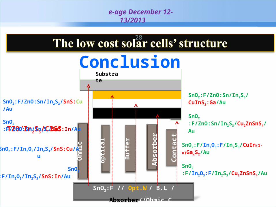
Substrate
SnO2:F // Opt.W / B.L / Absorber//Ohmic.C
opti
cal
win
dow
Oh
mic
con
tact
Ab
sorb
er
Con
tact
28
Bu
ffer
laye
rTZO/In2S3/CIGS
SnO2:F/ZnO:Sn/In2S3/SnS:Cu/Au
SnO2 :F/ZnO:Sn/In2S3/SnS:In/Au
SnO2:F/ZnO:Sn/In2S3/CuInS2:Ga/Au
SnO2 :F/ZnO:Sn/In2S3/Cu2ZnSnS4/Au
SnO2:F/In2O3/In2S3/SnS:Cu/Au
SnO2 :F/In2O3/In2S3/SnS:In/Au
SnO2:F/In2O3:F/In2S3/CuIn(1-x)GaxS2/Au
SnO2 :F/In2O3:F/In2S3/Cu2ZnSnS4/Au
Conclusion
e-age
December 12-13/2013

29
e-age December 12-13/2013