prathyusha - · pdf fileec2303 / computer architecture and organization 1 prathyusha institute...
TRANSCRIPT

EC2303 / Computer Architecture and Organization 1
PRATHYUSHAINSTITUTE OF TECHNOLOGY AND MANAGEMENT
DEPARTMENT OF INFORMATION TECHNOLOGY
Staff Name: Prof. S. Athinarayanan Branch: ECE / V SemUNIT – IV
PART – A
1. Define Memory Access Time and Memory Cycle Time.Ans:
Memory Access Time – is the time interval between the initiation and completion of Read or
Write Operation
Memory Cycle Time – is the minimum Time interval required between initiation of Two
successive memory operation.
2. Define Latency and bandwidth.Ans:
Latency – is the time interval, it takes to transfer a word of data from the memory
Bandwidth – is the amount of bytes of data transferred in one second.
3. Compare Static RAM and Dynamic RAM.Ans:
PARAMETER STATIC RAM DYNAMIC RAM
1. Cell Type Flip Flop Cell Capacitor Storage Cell
2. Speed Fast Slow
3. Refreshing Not Required Required
4. Density Less More
5. Cost More Less
4. What is the maximum size of the address space generated in a processor with has 32 bitaddress?
Ans:
The maximum size of the address space generated in a processor with has 32 bit
address = 232 = 4 Giga Locations.
5. What will be the number of address and data lines required for a 512K X 8 memorysystem?
Ans:
No. of address lines = 19
No. of data lines = 8

EC2303 / Computer Architecture and Organization 2
6. How many 128 X 4 RAM memory chips are required to build RAM memory system of1K bytes?
Ans:
Total No. of Chips = Total Memory Bits / Memory Bits per chip
No. of Chips Required = (1024 X 8) / (128 X 4) = 16
7. How many memory chips are required to construct 8M X 32 memory using 512K X 8chip?
Ans:
No. of Memory Chips required = (8M X 32) / (512 X 8) = 64
8. How many 128 X 8 RAM chips are needed to provide a memory capacity of 4K bytes?Ans:
No. of Memory Chips required = (4096 X 8) / (128 X 8) = 32
9. An application program in a computer with cache uses 1400 instruction fetch fromcache and 100 from main memory. What is hit ratio?
Ans:
Hit Ratio = No. of Instruction fetch from cache / Total no. of instructions
= 1400 / 1500 = 93.333%
10. Show how the virtual address translation divides the 32bit address with page size 16K.Ans:
Page size = 16K No. of address bits = 14
No. of bits for page numbers = 32 – 14 = 18 bits
Page Number Page offset
18 14
11. Explain the two possible address assignment for bytes with a word of 32bits.Ans:
Big-endian: The lower address is assigned to the most significant part of the word.
Little-endian: The Lower address is assigned to the least significant part of the word.
Big-endian Arrangement Little-endian ArrangementWord address Byte address Word address Byte address
0 0 1 2 3
4 4 5 6 7
.
.
.
2k-4 2k-4 2k-3 2k-2 2k-1
0 3 2 1 0
4 7 6 5 4
.
.
.
2k-4 2k-1 2k-2 2k-3 2k-4

EC2303 / Computer Architecture and Organization 3
12. Consider a two level cache with access time 5 nsec and 80 nsec respectively. If the hit
ratio are 95% and 75% respectively in the two caches and main memory access time is
250 nsec. What is the effective access time?
Ans:
Access Time = H1T1 + H2 (1 – H1)T2 + (1 – H1)(1 – H2)T3
= .95(5) + (1 - .95).75 X 80 -> (1-.95) (1-.75)250
= 4.75 + 3.00 + 3.125 = 10.875 nsec
13. Define Locality of Reference.Ans:
The locality of reference can be grouped into two types:
i) Spatial locality
Instruction in close proximity to the recently executed
instruction is likely to be executed soon
ii) Temporal locality
Recently an executed instruction is likely to be executed
again very soon.
14. What are the cache write protocols? Briefly explain.Ans:
There are two types of cache write protocols
i) Write Thru:
The Cache locations and the main memory location are
updated simultaneously.
ii) Write Back:
Here the cache location is updated and it is marked dirty. The
main memory location is updated later when the block is marked
dirty is to be removed from the cache to make room for a new block.
15. What are the cache mapping algorithms?Ans:
1. Direct Mapping
2. Associative Cache
3. Set Associative Cache
16. Give the expression for average access time for a memory system with cache.Ans:
The effective access time Tav = hc + (1 – h)M
where c be the access time to cacheM be the access time of Main memoryh be the hit ratio
EC2303 / Computer Architecture and Organization 4
17. What are memory interleaving and its advantage?
Ans:
In Memory interleaving the successive address are located in successive modules. i.e.
the low order address select the module, the high order address select the word within the
block. This results in faster transfer of Block of Data. This method is called Interleaving.
18. Compute the number of external pins required for 1K X 1 memory chip.
Ans:
No. of external pins required = 15 (Address Lines – 10, Data Line – 1, Control Line –
2[R/W & CS], power and ground – 2)
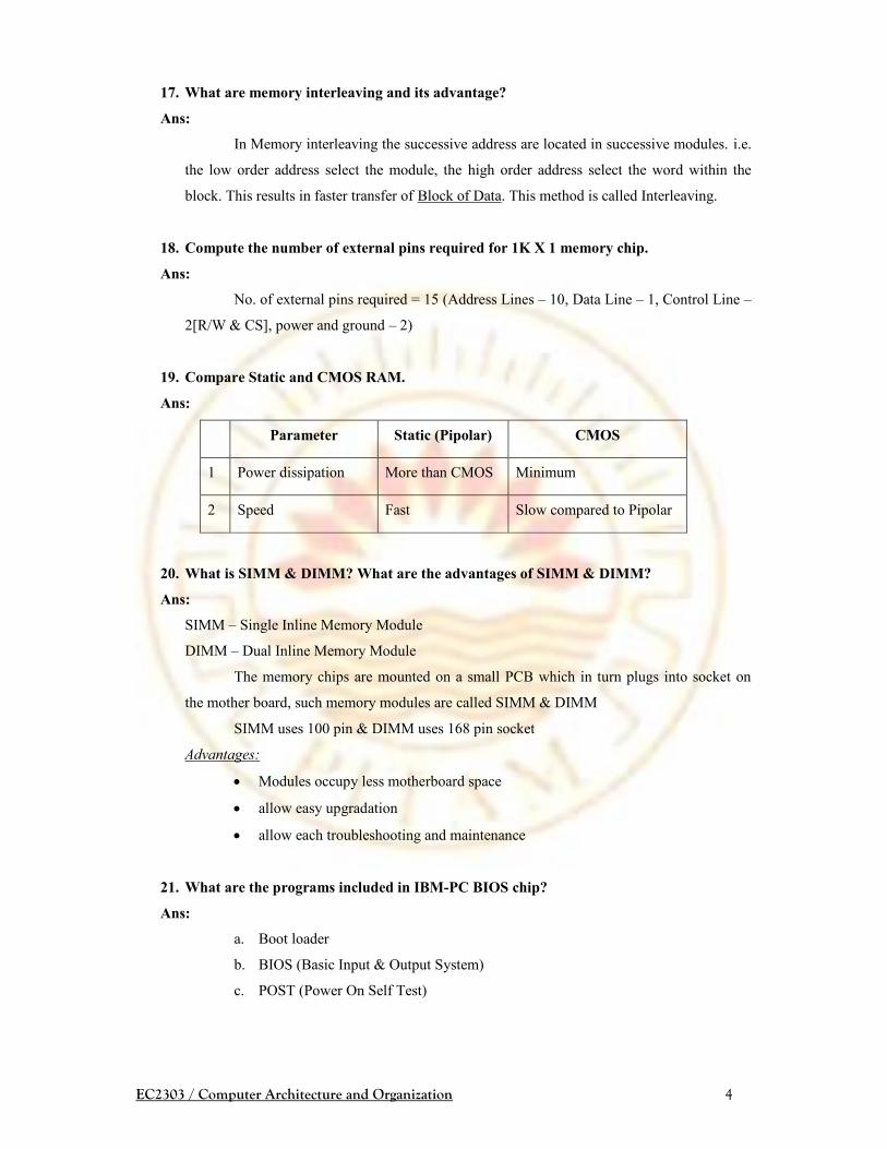
19. Compare Static and CMOS RAM.
Ans:
Parameter Static (Pipolar) CMOS
1 Power dissipation More than CMOS Minimum
2 Speed Fast Slow compared to Pipolar
20. What is SIMM & DIMM? What are the advantages of SIMM & DIMM?
Ans:
SIMM – Single Inline Memory Module
DIMM – Dual Inline Memory Module
The memory chips are mounted on a small PCB which in turn plugs into socket on
the mother board, such memory modules are called SIMM & DIMM
SIMM uses 100 pin & DIMM uses 168 pin socket
Advantages:
Modules occupy less motherboard space
allow easy upgradation
allow each troubleshooting and maintenance
21. What are the programs included in IBM-PC BIOS chip?
Ans:
a. Boot loader
b. BIOS (Basic Input & Output System)
c. POST (Power On Self Test)
EC2303 / Computer Architecture and Organization 5
22. Compare SRAM, DRAM and hard disk Technology with respect to Speed, Size andCost.
Ans:Comparison of SRAM, DRAM and Hard Disk Technology
Technology Speed Size Cost
SRAM Fast MemoryLarge memory impractical
only small
Costly due to 6Transistor
cell
DRAM Slow Compared To SRAMModerately large memory
can be built
Cost less due to
1Transistor cell
HARD DISKMuch slower due to
rotational access time
A huge memory can be
built
Lower cost compared to
semi conductor memory
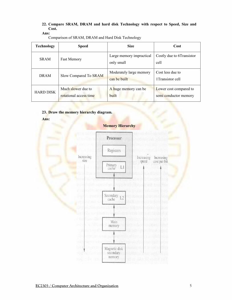
23. Draw the memory hierarchy diagram.
Ans:
Memory Hierarchy

EC2303 / Computer Architecture and Organization 6
24. Draw the SRAM & DRAM cell diagram.
Ans:
Bipolar Static RAM
CMOS STATIC RAM
Asynchronous Dynamic RAM (DRAM)

EC2303 / Computer Architecture and Organization 7
25. What are Cache replacement algorithms?
Ans:
Cache Replacement Algorithms
1. first in first out
2. Least Recently used
3. Random Replacement
26. What is RAM & Serial Access Memory?
Ans:
In Random Access Memory (RAM) any location can be accessed for a Read or Write
operation in some fixed time that is independent of location’s address.
In Serial Access Memory the access time depends on the address or position of the
data.
EC2303 / Computer Architecture and Organization 8
PART – B
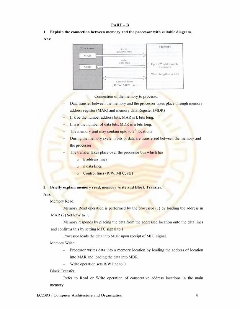
1. Explain the connection between memory and the processor with suitable diagram.
Ans:
Connection of the memory to processor
- Data transfer between the memory and the processor takes place through memory
address register (MAR) and memory data Register (MDR)
- If k be the number address bits, MAR is k bits long.
- If n is the number of data bits, MDR is n bits long.
- The memory unit may contain upto to 2K locations
- During the memory cycle, n bits of data are transferred between the memory and
the processor
- The transfer takes place over the processor bus which has
o k address lines
o n data lines
o Control lines (R/W, MFC, etc)
2. Briefly explain memory read, memory write and Block Transfer.
Ans:
Memory Read:
Memory Read operation is performed by the processor (1) by loading the address in
MAR (2) Set R/W to 1.
Memory responds by placing the data from the addressed location onto the data lines
and confirms this by setting MFC signal to 1.
Processor loads the data into MDR upon receipt of MFC signal.
Memory Write:
- Processor writes data into a memory location by loading the address of location
into MAR and loading the data into MDR
- Write operation sets R/W line to 0.
Block Transfer:
Refer to Read or Write operation of consecutive address locations in the main
memory.

EC2303 / Computer Architecture and Organization 9
3. Explain internal organization of 16 X 8 memory chip with suitable diagram.
Ans:
Fig gives the internal organization of a small memory chip consisting of 16 words of 8 bit
each.
Each row of cells constitute a memory word
All cells of a row are connected to a common line known as word line which is driven by
address decoder
Every column of cells are connected to sense / write circuit by two lines.
The sense / write circuit is connected to data input / output lines of the chip.
During Read, the information stored in the cells selected by the word line transmits this
information to the output lines
During write operation the sense / write circuit receive input information and store it in
the cells selected by word line
Internal Orgranisation of 16 X 8 memory chip
EC2303 / Computer Architecture and Organization 10
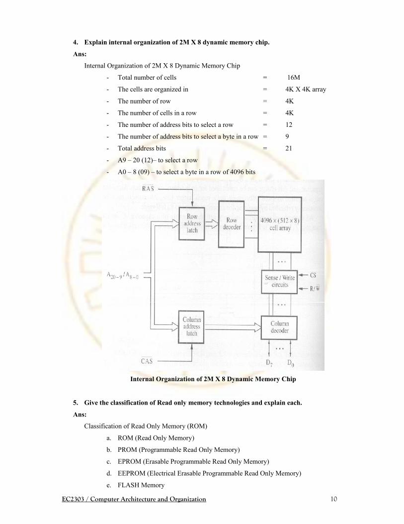
4. Explain internal organization of 2M X 8 dynamic memory chip.
Ans:
Internal Organization of 2M X 8 Dynamic Memory Chip
- Total number of cells = 16M
- The cells are organized in = 4K X 4K array
- The number of row = 4K
- The number of cells in a row = 4K
- The number of address bits to select a row = 12
- The number of address bits to select a byte in a row = 9
- Total address bits = 21
- A9 – 20 (12)– to select a row
- A0 – 8 (09) – to select a byte in a row of 4096 bits
Internal Organization of 2M X 8 Dynamic Memory Chip
5. Give the classification of Read only memory technologies and explain each.
Ans:
Classification of Read Only Memory (ROM)
a. ROM (Read Only Memory)
b. PROM (Programmable Read Only Memory)
c. EPROM (Erasable Programmable Read Only Memory)
d. EEPROM (Electrical Erasable Programmable Read Only Memory)
e. FLASH Memory

EC2303 / Computer Architecture and Organization 11
a. ROM (Read Only Memory)
Read Only Memory CELL
- ROM Cell used only one transistor and storage element
- The Logic ‘0’ is stored, if storage element is shorted
- The logic ‘1’ is stored, if storage element is open
- Read operation is done by activating word line
- Write operation is performed during manufacturing
Advantage:
Less costly for large volume production
Disadvantage:
Not programmable
b. PROM (Programmable Read Only Memory)
- This allows data to be written by user
- Programmability is achieved by inserting a fuse at point P
- Before programming, the memory contain all 0’s and user can insert 1 by burning
the fuse by high current
Advantage:
Programmable by user
Disadvantage:
Once programmed, chip content can not be altered, i.e. can not be reprogrammed
c. EPROM (Erasable Programmable Read Only Memory)
- Here stored data can be erased and new data can be written
- The fuse in the PROM is replace by a special Transistor (which can act as a open
switch or closed switch)
- Here data can be written by injecting current pulse like PROM (0 to 1)
- The memory content can be erased by exposing to ultraviolet. During erasing
trapped charge dissipate and cell becomes 0.
- Hence EPROM chip are mounted with transparent window.
Advantage:
Reprogramming makes flexible for development

EC2303 / Computer Architecture and Organization 12
Disadvantage:
Erasure need chip to remove from the board and exposure to UV light.
d. EEPROM
- Here both programming and erasing is done with electric pulse
- The voltages needed for erasing, writing and reading are different
Advantage:
Reprogramming can be done on board (new version of program can be loaded online)
Disadvantage:
Costly compared to EPROM
Different voltage for Erasing and Writing & Erasing
e. FLASH
This is similar to EEPROM except
- In EEPROM, it is possible to read and write the content of a single cell
- In flash, it is possible to read the content of a single cell but it is possible to write
entire block of cells.
- Before writing, the previous contents of the block are erased.
Advantage:
- has higher density which leads to higher capacity and lower cost per bit than
EEPROM
- Reprogramming on board
- Low power consumption hence used in battery operated device
Disadvantage:
A single cell can not be written, only entire block can be written.
Examples 1. Flash cards / Pen Drives, Flash drives
6. What is cache memory and explain the various mapping algorithms.
Ans:
A small, fast memory introduced between the processor and the main memory is
called cache memory which improves the effective speed of the memory.
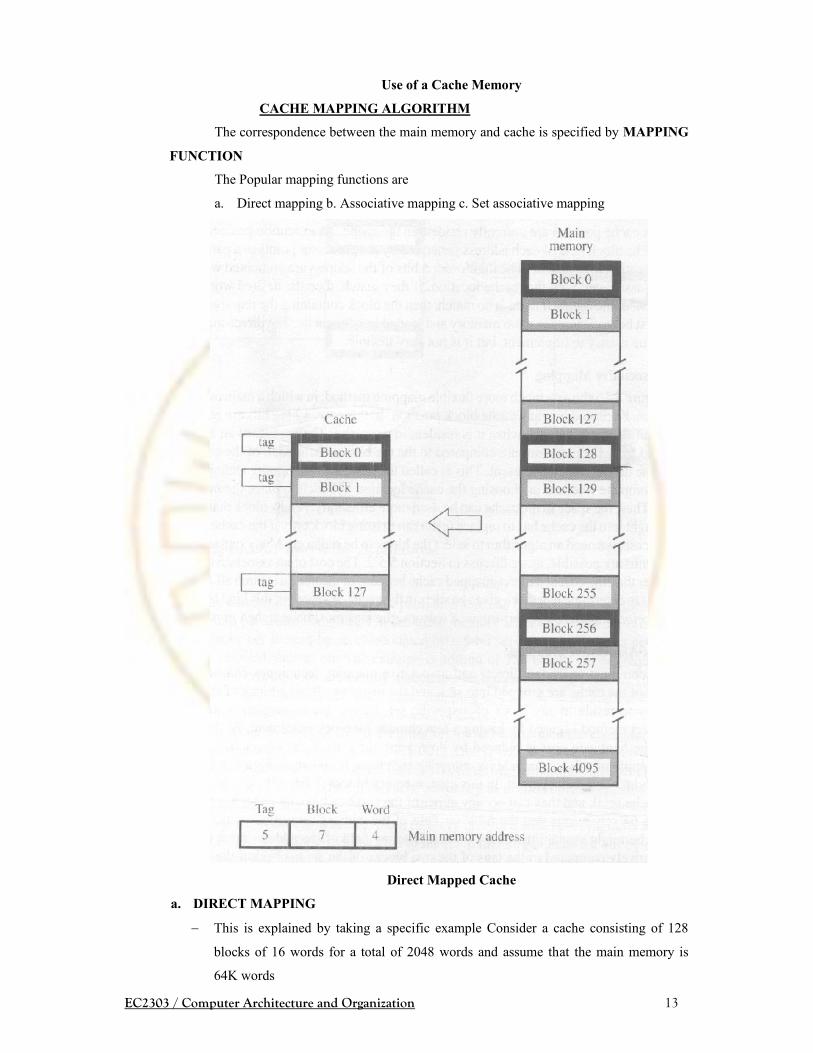
EC2303 / Computer Architecture and Organization 13
Use of a Cache Memory
CACHE MAPPING ALGORITHM
The correspondence between the main memory and cache is specified by MAPPING
FUNCTION
The Popular mapping functions are
a. Direct mapping b. Associative mapping c. Set associative mapping
Direct Mapped Cache
a. DIRECT MAPPING
This is explained by taking a specific example Consider a cache consisting of 128
blocks of 16 words for a total of 2048 words and assume that the main memory is
64K words

EC2303 / Computer Architecture and Organization 14
Both main memory and cache memory is divided into blocks of size equal to 16
words
Here block j of main memory maps to (block j mod 128) of cache.
Main memory blocks 0, 128, 256 … loaded into cache block 0
Main memory blocks 1, 129, 257 … loaded into cache block 1 and so on
Placement of a block in the cache is determined from memory address
Memory address is divided into three fields as shown in figure
Lower order 4 bit select one of 16 words within a block
Next 7 bits select cache block
Next 5 bit decides block from which segment is mapped to cache.
During processing higher order 5 bits are compared with tag bits of cache block
pointed by 7 bit cache block field
If match – desired word is in the block
– Cache Hit
If not – desired word is brought from main memory and loaded to cache
– Cache Miss
Advantages:
It is easy to implement.
Disadvantages:
Contention
b. ASSOCIATIVE MAPPING

EC2303 / Computer Architecture and Organization 15
Associative Mapping
- Here any main memory block can be loaded into any cache block
- which block of main memory is loaded in each cache block is indicated by Tag
bits – (12 bits)
- During operation the Tag bits of the address received will be compared to the Tag
bits of each block of the cache to see the desired block is in cache
- This is called Associative Mapping Technique
- The new block has to be brought into the cache has to replace the existing block
only if the cache is full and we use Replacement algorithm
c. SET ASSOCIATIVE MAPPING
Set Associative Mapping
This mapping is the combination of direct mapping and associative mapping
technique. The same cache size 2K words organized into two blocks per set.
Block j of main block is mapped into (j mod 64) of cache block
- memory blocks 0, 64, 128 … mapped to cache set 0 and they can occupy either of
two blocks position within the set
- memory blocks 1, 65, 129 … mapped to cache set 1 and so on
During operation 6 bit set field give the set which contain the data and 6 bit Tag of
address is associatively compared to the tags of the two blocks of the set to check the desired
data is in cache.

EC2303 / Computer Architecture and Organization 16
- The number of blocks per set is a parameter that can be selected to suit the
requirement of a particular computer
- A cache that has K blocks per set is referred as a K way set associative cache.
7. What is virtual memory and explain the virtual memory address translation.
Ans:
In a Computer system (without virtual storage) the program size is limited by the physical
memory available in the system.
However the virtual memory system extends the apparent size of the physical memory equal
to the address space of the processor.
The address translation from the virtual address to the physical address is carried out by a unit
called Memory Management Unit (MMU) as shown in diagram below.
Virtual Memory Organisation
EC2303 / Computer Architecture and Organization 17
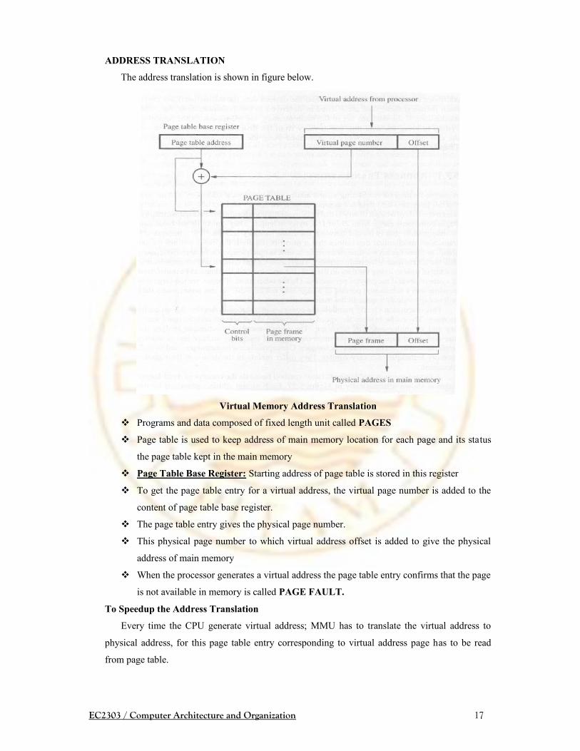
ADDRESS TRANSLATION
The address translation is shown in figure below.
Virtual Memory Address Translation
Programs and data composed of fixed length unit called PAGES
Page table is used to keep address of main memory location for each page and its status
the page table kept in the main memory
Page Table Base Register: Starting address of page table is stored in this register
To get the page table entry for a virtual address, the virtual page number is added to the
content of page table base register.
The page table entry gives the physical page number.
This physical page number to which virtual address offset is added to give the physical
address of main memory
When the processor generates a virtual address the page table entry confirms that the page
is not available in memory is called PAGE FAULT.
To Speedup the Address Translation
Every time the CPU generate virtual address; MMU has to translate the virtual address to
physical address, for this page table entry corresponding to virtual address page has to be read
from page table.

EC2303 / Computer Architecture and Organization 18
Use of an associative mapped TLB
To avoid this access time and degradation of performance, recently translated virtual page and
its corresponding physical page is kept in a buffer and this buffer is called Translation Look
aside Buffer (TLB)
When a processor i.e. MMU finds the page table entries in TLB, it does not have to access the
page table and saves substantial access time.
8. List three secondary storage devices and briefly explain Magnetic Hard Disk.
Ans:
Secondary Storage Devices
- A huge amount of cost effective storage is provided by secondary storage
devices.
- Popular secondary storage devices.
o Magnetic Hard Disk
o Magnetic Tape
o Optical Disks

EC2303 / Computer Architecture and Organization 19
i) Magnetic Hard Disk
Medium:
The storage medium in a magnetic disk consists of one or more disk mounted on a
common spindle.
A thin magnetic film is deposited on each disk usually on both sides
The common spindle is connected to a rotary drive so that magnetic surface is in
close proximity to read / write head
- Digital information is stored on the magnetic film by applying current pulse
- Read / Write head must be maintained at a very small distance in order to achieve
high density and reliable read / write operation.
- During reading the change in magnetic field caused by the film movement induce
the voltage in the coil.
Winchester Technology:
In modern disk units, the disk and the read / write are placed in a sealed air filtered
enclosure. This approach is called Winchester Technology.
- In this approach Read / Write heads can be more closer to the surface
- Since the head are closer, data density can be more.
EC2303 / Computer Architecture and Organization 20
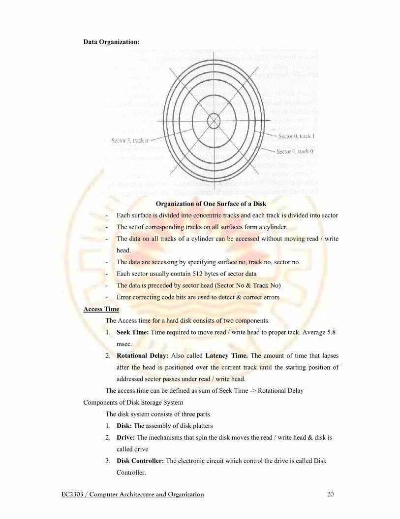
Data Organization:
Organization of One Surface of a Disk
- Each surface is divided into concentric tracks and each track is divided into sector
- The set of corresponding tracks on all surfaces form a cylinder.
- The data on all tracks of a cylinder can be accessed without moving read / write
head.
- The data are accessing by specifying surface no, track no, sector no.
- Each sector usually contain 512 bytes of sector data
- The data is preceded by sector head (Sector No & Track No)
- Error correcting code bits are used to detect & correct errors
Access Time
The Access time for a hard disk consists of two components.
1. Seek Time: Time required to move read / write head to proper tack. Average 5.8
msec.
2. Rotational Delay: Also called Latency Time. The amount of time that lapses
after the head is positioned over the current track until the starting position of
addressed sector passes under read / write head.
The access time can be defined as sum of Seek Time -> Rotational Delay
Components of Disk Storage System
The disk system consists of three parts
1. Disk: The assembly of disk platters
2. Drive: The mechanisms that spin the disk moves the read / write head & disk is
called drive
3. Disk Controller: The electronic circuit which control the drive is called Disk
Controller.
EC2303 / Computer Architecture and Organization 21
9. Briefly Explain about Optical Drives.
Ans:
The popular Optical Storage Devices are
a. CD Technology
b. DVD Technology
c. Blue Ray Technology
a. CD Technology (Compact Disk ROM)
- CD Technology is based on Laser source (infra red laser)
- The Laser beam is directed onto the surface of spinning disk
- Physical indentation in the surface are arranged along the track of disk
- The reflect the focused beam towards a photo detector which detects stored
binary pattern
Physical Description
- CD is 120mm in diameter and thickness is 1.2mm
- Bottom layer is polycarbonate plastic
- The surface of plastic is made bit & lands (to reflect data)
- A thin layer of aluminum is placed on the top of programmed disk
- The laser source and photo detector is place below polycarbonate plastic
- when the laser encounts pits & lands get reflected and bright beam
- When the laser encounter transistion pit to land or land to pit the reflected light is
180* out of phase and cancel each other and hence dark beam
- Actual data of 8bit is converted to 14bit for recording on CD.
Data Recording
- The data is recorded on spiral tracks
- The space between tracks 1.6 Micron
- Pits are .5micron wide and .8 to 3 micron long
- Data is organized in the form of sectors
Speed
CD operate at different speed
- At basic speed 1x, 75 sectors per second
- The data rate is 150 Kbytes
- CD is designed for 75 minutes of music and storage capacity of 650 Mbytes
- 40x CD has a transfer rate 40 times higher than 1x CDROM
Advantage:
- Small size
- Low cost
- Portable

EC2303 / Computer Architecture and Organization 22
Disadvantage:
- 1x data rate is lower
- seek time is more
CDROM
- data is recorded during its manufacturing
CD Recordable – (CD – R)
- This can be burned / written with data
Disadvantage – can not be rewritten
CD Rewritable (CD – R / W)
- This can be used to write multiple times
Advantage – can be used for taking backup
b. DVD Technology (Digital Versatile Disk)
- Physical media is identical to CDROM
- Capacity
o Single Side = 4.7G Bytes
o Single Side Double Layer = 8.5 G Bytes
o Double Side Single Layer = 9.4 G Bytes
o Double Side Double Layer = 17 G Bytes
DVD – ROM, DVD – R, DVD – R/W are identical to CD – ROM, CD –R, CD – R/W
c. Blue Ray Technology
- Physical media is identical to CDROM
- Capacity – 25 G Bytes
- Uses Blue – Violet Lasers (405 nanometers)

EC2303 / Computer Architecture and Organization 23
10. Design 2M X 32 memory system using 512K X 8 static memory chips and draw the
diagram.
Ans:
The no. of chips required = 2M X 32 / 512K X 8 = 16. These chips are arranged in
four rows and four columns as shown in diagram.
Arrangement of memory system 2M X 32 using 512K X 8 static memory chips

EC2303 / Computer Architecture and Organization 24
11. Explain with diagram about associative memory.
Ans:
Associative Memory
Associative memory is one in which any stored item can be accessed directly by
using the content of the item generally some specified subfield as an address.
Associative memory is also called Content Addressable Memory (CAM)
The subfield to address the memory is called Key
Organization of Associative Memory
Structure of Associative memory
The figure shows the structure of an associative memory
Each unit of stored information is a fixed length word
Any subfield of the word can be chosen as the key
The desired key is specified by a mask Register whose content identify the bit
position that define the key (need not be adjacent)

EC2303 / Computer Architecture and Organization 25
The current key is compared simultaneously with all stored words, those that match
the key output a match signal which enters a select circuit.
The select circuit enables the data field to be accessed
Since all words in the memory are required to compare their keys with input key
simultaneously each needs its own match circuit
The match and select circuits make associative memories more complex and
expensive than conventional memories.
VLSI Technology makes this associative memory feasible and still costly.
Associative Memory Cell
The logic circuit of 1 bit Associative memory is shown in diagram. This comprises
The cell is D Flip Flop for data storage
The match circuit (exclusive Nor gate) for comparing the F/F content to an external
data bit D
Circuit for reading (Select)
Circuit for writing (WE & Select)
The results of comparison appears on match output M when M = 1 denotes match and
M = 0 denotes no match.
The cell is select4ed by addressed for both read and write operation by setting select
line S = 1
New data is written into the cell by setting WE = 1 which in turn enables D F/F clock
input
The stored data can be read out via Q line
The mask control line MK is activated (MK = 1) to force the match line M to 0
independent of the data stored in the D F/F
MK also disables the input circuit of F/F by forcing CK = 1
Disadvantages
o The cell of this type needs about 10 transistors for more than single transistor
required for dynamic ram.
o Hence the associative memory is costly, large associative memory are rarely used
outside cache.