practical design techniques for sensor signal conditioning ... · sensor signal conditioning 1...
TRANSCRIPT

a 9.0
PRACTICAL DESIGN TECHNIQUES FORSENSOR SIGNAL CONDITIONING
1 Introduction
2 Bridge Circuits
3 Amplifiers for Signal Conditioning
4 Strain, Force, Pressure, and Flow Measurements
5 High Impedance Sensors
6 Position and Motion Sensors
7 Temperature Sensors
8 ADCs for Signal Conditioning
n 9 Smart Sensors
10 Hardware Design Techniques
a 9.1
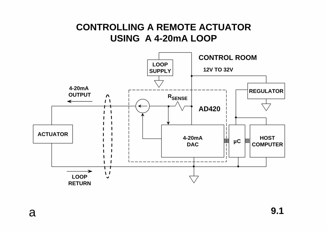
CONTROLLING A REMOTE ACTUATORUSING A 4-20mA LOOP
4-20mADAC
µCHOST
COMPUTER
REGULATOR
LOOPSUPPLY
RSENSE
CONTROL ROOM
4-20mA OUTPUT
ACTUATOR
AD420
12V TO 32V
LOOPRETURN

a 9.2
4-20mA LOOP POWERED SMART SENSORS
EN
SO
R
ADC µC4-20mA
DAC
RSENSE
AD421
ICOMMON < 4.00mA
ADC µCHOST
COMPUTER
REGULATORLOOP
SUPPLY
RSENSE
3.3V / 5V
AD7714/AD7715
IAD421 < 0.75mA
CONTROL ROOMDMOS FET
DMOS FET: Supertex DN2535 Siliconix ND2020L or ND2410L
4-20mA RETURN
LOOPPOWER
I µC+SENSOR < 2.75mA
I AD7714/AD7715 < 0.50mA
ICOMMON

a 9.3
HART INTELLIGENT REMOTE TRANSMITTERUSING AD421 LOOP-POWERED 4-20mA DAC
SE
NS
OR
ADC µC4-20mA
DACAD421
HARTMODEM
BELL 202
WAVEFORMSHAPER
BANDPASSFILTER
LOOP POWER
LOOP RETURN
CC
HT20C12 / 20C15 (Symbios Logic)
HART DIGITAL SIGNAL: 1200Hz, 2200Hz FREQUENCY SHIFT KEYING (FSK)

a 9.4
INDUSTRIAL NETWORKING
NODEFIELD NETWORK NODEN
OD
EBRANCHN
OD
ES
MA
RT
SE
NS
OR
SM
AR
T S
EN
SO
R
DE
VIC
E N
ET
WO
RK
SMART SENSOR
SMART SENSOR
a 9.5
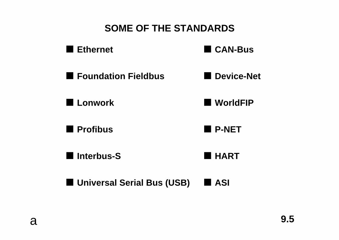
SOME OF THE STANDARDS
n Ethernet
n Foundation Fieldbus
n Lonwork
n Profibus
n Interbus-S
n Universal Serial Bus (USB)
n CAN-Bus
n Device-Net
n WorldFIP
n P-NET
n HART
n ASI

a 9.6
THE IEEE 1451.2 SENSOR INTERFACE STANDARD
NCAP FIELD NETWORK - OR - DEVICE NETWORK
TII
ST
IM
TEDS
Sensoror
Actuator
n NCAP = Network Capable ApplicationProcessor
n TII = Transducer IndependentInterface
n TEDS = Transducer Electronic Datasheet
n STIM = Smart Transducer InterfaceModule
a 9.7
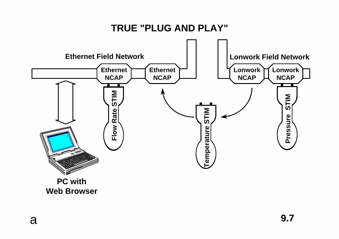
TRUE "PLUG AND PLAY"
LonworkNCAP
EthernetNCAP
EthernetNCAP
PC withWeb Browser
LonworkNCAP
Ethernet Field Network Lonwork Field Network
Flo
w R
ate
ST
IM
Tem
per
atu
re S
TIM
Pre
ssu
re S
TIM

a 9.8
THE SMART SENSOR
Precision Amplifier
High Resolution ADC
Microcontroller Sensor
Pressure Sensor,RTD, Thermocouple,Strain Gage,etc.
a 9.9
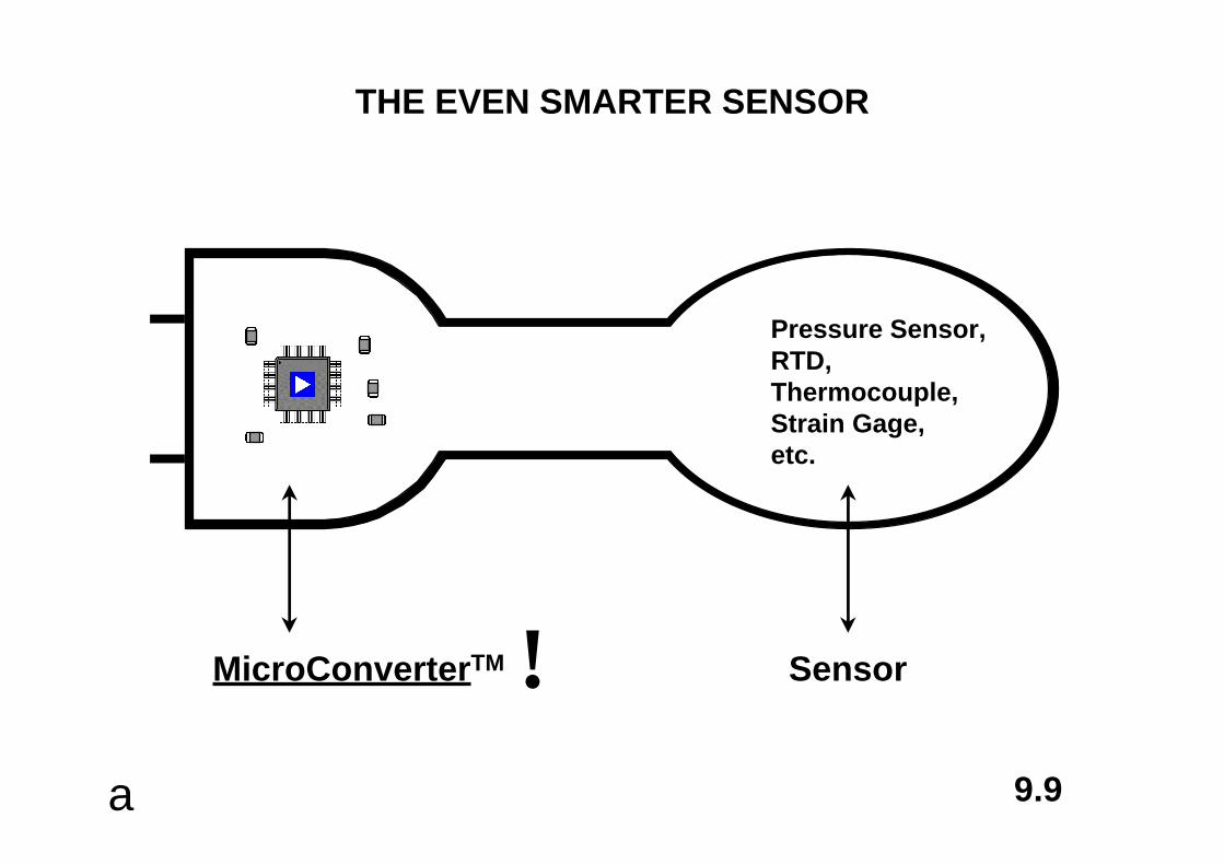
THE EVEN SMARTER SENSOR
SensorMicroConverterTM !
Pressure Sensor,RTD, Thermocouple,Strain Gage,etc.

a 9.10
THE MicroConverter™
High Performance Analog I/O
+
On-Chip FLASH Memory
+
On-Chip Microcontroller
1
2
3
=
MicroConverter™

a 9.11
ANALOG I/O 1
n Dual Σ∆Σ∆ ADCu >16 bitu >100dB SNR (p-p)u Differential Inputsu Prog. Gain Ampu Self-Calibration
n 12bit V-Out DACu < ½ LSB DNL
n Voltage Reference
n Temperature Sensor
n 8 chan SAR ADCu 10 bitu < ½ LSB INL
n 12bit V-Out DACu < ½ LSB DNL
n Voltage Reference
n Temperature Sensor
n 8 chan SAR ADCu 12 bit, 5µsu < ½ LSB INLu DMA modeu Self-Calibration
n Dual 12bit V-Out DACu < ½ LSB DNL
n Voltage Reference
n Temperature Sensor
ADuC816 ADuC812 ADuC810

a 9.12
ON-CHIP FLASH MEMORY 2
n 8K bytes Nonvolatile FLASH Program Memoryu Stores Program and Fixed Lookup Tablesu In-Circuit Serial Programmable or External Parallel Programmableu Read-Only to Microprocessor Core
n 640 bytes Nonvolatile FLASH Data Memoryu User “Scratch Pad” for Storing Data During Program Executionu Simple Read / Write Access Through SFR Space
n Programming Voltage (VPP) Generated On-Chip
ADuC816 ; ADuC812 ; ADuC810

a 9.13
ON-CHIP MICROCONTROLLER 3
n Industry Standard 8052 Coreu 12 Clock Machine Cycle w/ up to 16MHz Clocku 32 Digital I/O Pinsu Three 16bit Counter/Timersu Universal Asynchronous Receiver/Transmitter
(UART) Serial Port
n ...Plus Some Useful Extrasu SPI or I2C Compatible Serial Interfaceu WatchDog Timeru Power Supply Monitoru Timer Interval Counter (ADuC816/810)
ADuC816 ; ADuC812 ; ADuC810

a 9.14
ADuC816 FUNCTIONAL BLOCK DIAGRAM
AINMUX
AINMUX
buf pga Σ∆Σ∆ ADC
ADCcontrol
andcalibration
Σ∆ Σ∆ ADC
ADCcontrol
andcalibration
TEMPsensor
2.5Vbandgapreference
VREFdetect
8K x 8programFLASH
EEPROM
640 x 8user FLASH
synchronousserial interface(SPI or I2C)
8052micro-
controllercore
256 x 8user RAM
watchdogtimer
power supplymonitor
asynchronousserial port(UART)
16 bitcountertimers
timerintervalcounter
OSC &PLL
DACcontrol
DAC1buf
buf
AV
DD
AG
ND
DV
DD
DG
ND
SC
LK
SD
AT
A/
MO
SI
MIS
OS
S
AL
E
PS
EN
EA
RE
SE
T
RxD
TxD
XT
AL
1
XT
AL
2
(primary channel)
(auxilliary channel)
AIN1
AIN2
AIN3
AIN4
VREFIN+
VREFIN–
IEXC1
IEXC2
DAC
T0
T1T2
T2EX
INT0
INT1
–3.5mV/°C
ADuC816
5 6 20 34 47 21 35 48 26 27 14 13 42 41 40 15 16 17 32 33
43 44 45 46 49 50 51 52 1 2 3 4 9 10 11 12 28 29 30 31 36 37 38 39 16 17 18 19 22 23 24 25
910
1112
8
7
3
4
10
22
23
1
2
18
19
P0.
0P
0.1
P0.
2P
0.3
P0.
4P
0.5
P0.
6P
0.7
P1.
0P
1.1
P1.
2P
1.3
P1.
4P
1.5
P1.
6P
1.7
P2.
0P
2.1
P2.
2P
2.3
P2.
4P
2.5
P2.
6P
2.7
P3.
0P
3.1
P3.
2P
3.3
P3.
4P
3.5
P3.
6P
3.7

a 9.15
ADuC816 - PRIMARY SPECIFICATIONS
n ADC : INL - ± 30ppmSNR (p-p) - >102dB (17 Noise Free Bits)Input Range - ± 20mV to ± 2.56VConv. Rate - 5.4Hz to 105Hz
n DAC : DNL - ± ½LSBOutput Range - 0 to VREF -or- 0 to VDDSettling Time - <4µs
n Power : Specified for 3V or 5V Operation5V 3V
Normal 7mA 3mAIdle 4.5mA 1.5mAPowerdown <20µA <20µA
a 9.16
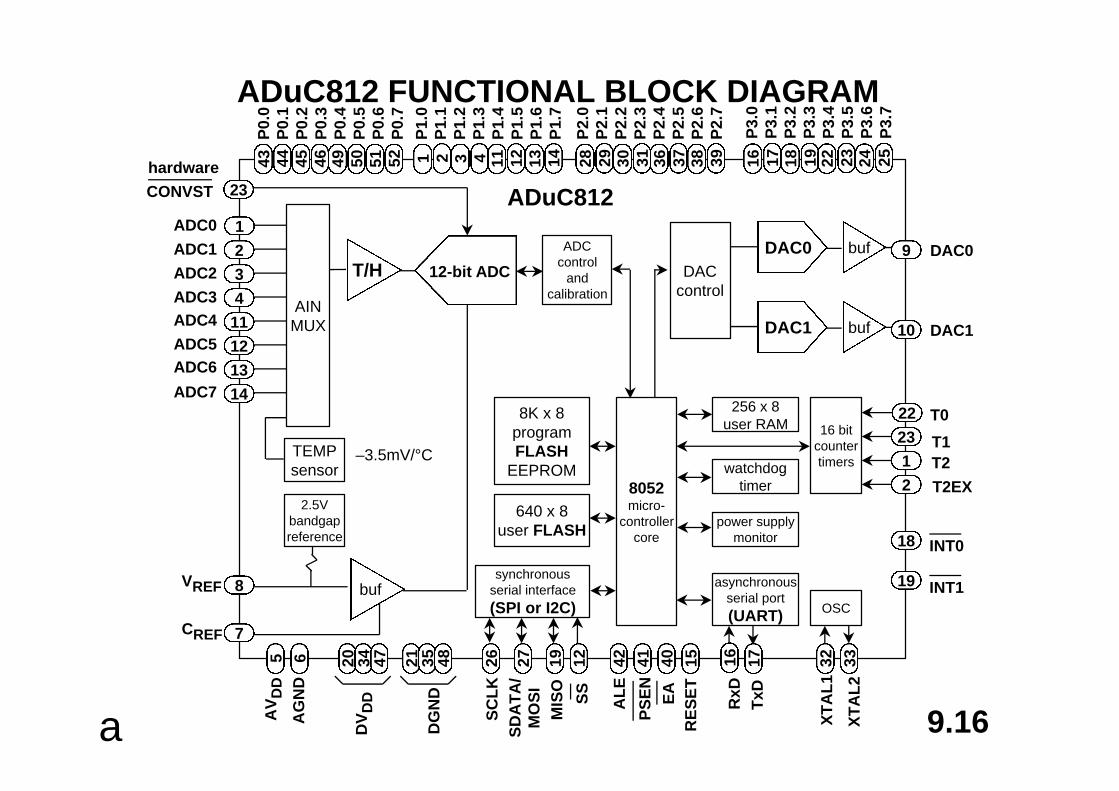
ADuC812 FUNCTIONAL BLOCK DIAGRAM
AINMUX
T/H 12-bit ADC ADC
controland
calibration
TEMPsensor
2.5Vbandgapreference
8K x 8programFLASH
EEPROM
640 x 8user FLASH
synchronousserial interface(SPI or I2C)
8052micro-
controllercore
256 x 8user RAM
watchdogtimer
power supplymonitor
asynchronousserial port(UART)
16 bitcountertimers
OSC
DACcontrol
DAC1 buf
AV
DD
AG
ND
SC
LK
SD
AT
A/
MO
SI
MIS
O
SS
AL
E
PS
EN
EA
RE
SE
T
RxD
TxD
XT
AL
1
XT
AL
2
ADC0
ADC1
ADC3ADC4
VREF
DAC1
T0
T1T2
T2EX
INT0
INT1
–3.5mV/°C
ADuC812
ADC2
ADC5ADC6
ADC7
CREF
DAC0 buf DAC0
buf
CONVST
hardware 43 44 45 46 49 50 51 52 1 2 3 4 11 12 13 14 28 29 30 31 36 37 38 39 16 17 18 19 22 23 24 25
23
5
1
2
3
4
11
12
13
14
8
7
6 20 34 47 21 35 48 26 27 19 12 42 41 40 15 16 17 32 33
9
10
22
23
1
2
18
19
P0.
0P
0.1
P0.
2P
0.3
P0.
4P
0.5
P0.
6P
0.7
P1.
0P
1.1
P1.
2P
1.3
P1.
4P
1.5
P1.
6P
1.7
P2.
0P
2.1
P2.
2P
2.3
P2.
4P
2.5
P2.
6P
2.7
P3.
0P
3.1
P3.
2P
3.3
P3.
4P
3.5
P3.
6P
3.7
DV
DD
DG
ND

a 9.17
ADuC812 - PRIMARY SPECIFICATIONS
n ADC : INL - ± ½LSBSNR (p-p) - >70dBInput Range - 0 to VREFConv. Time - <5µs (200kSPS)
n DAC : DNL - ± ½LSBOutput Range - 0 to VREF -or- 0 to VDDSettling Time - <4µs
n Power : Specified for 3V or 5V Operation5V 3V
Normal 18mA 12mAIdle 10mA 6mAPowerdown <50µA <50µA

a 9.18
MicroConverter™ DESIGN SUPPORT
MicroConverterTM
Web Site
QuickStartTM
Development Kit
Third PartyDevelopment Tools
1
2
3
a 9.19
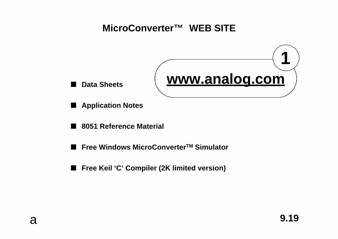
MicroConverter™ WEB SITE
www.analog.com1
n Data Sheets
n Application Notes
n 8051 Reference Material
n Free Windows MicroConverterTM Simulator
n Free Keil ‘C’ Compiler (2K limited version)

a 9.20
MicroConverter™ - QuickStart™ DEVELOPMENT KIT
n Documentationu User’s Guideu Datasheetu Tools Tutorialu Quick Reference Guide
n Evaluation Boardu RS-232 Serial Commsu 32K External SRAMu Buffered Analog I/O
n Regulated Power Supply
n Serial Port Cable
n Software
u Metalink Assembleru ‘C’ Compiler (Limited 2K)u Windows Simulatoru Serial Downloaderu Windows Debuggeru Example Code
QuickStartTM
2

a 9.21
MicroConverter™ - THIRD PARTY DEVELOPMENT TOOLS
n Keil Compileru A full function windows based ‘C’ compiler environment featuring
a simulator for source and assembly level debugging.
n MetaLink Emulatoru A high end in circuit emulation system offering a complete
windows based environment for in-system debug sessions.
Power Tools3
All tools will fully integrate with each MicroConverter product
The First Two of Many ThirdParty Tools to Fully SupportMicroConverterTM Products:
a 9.22
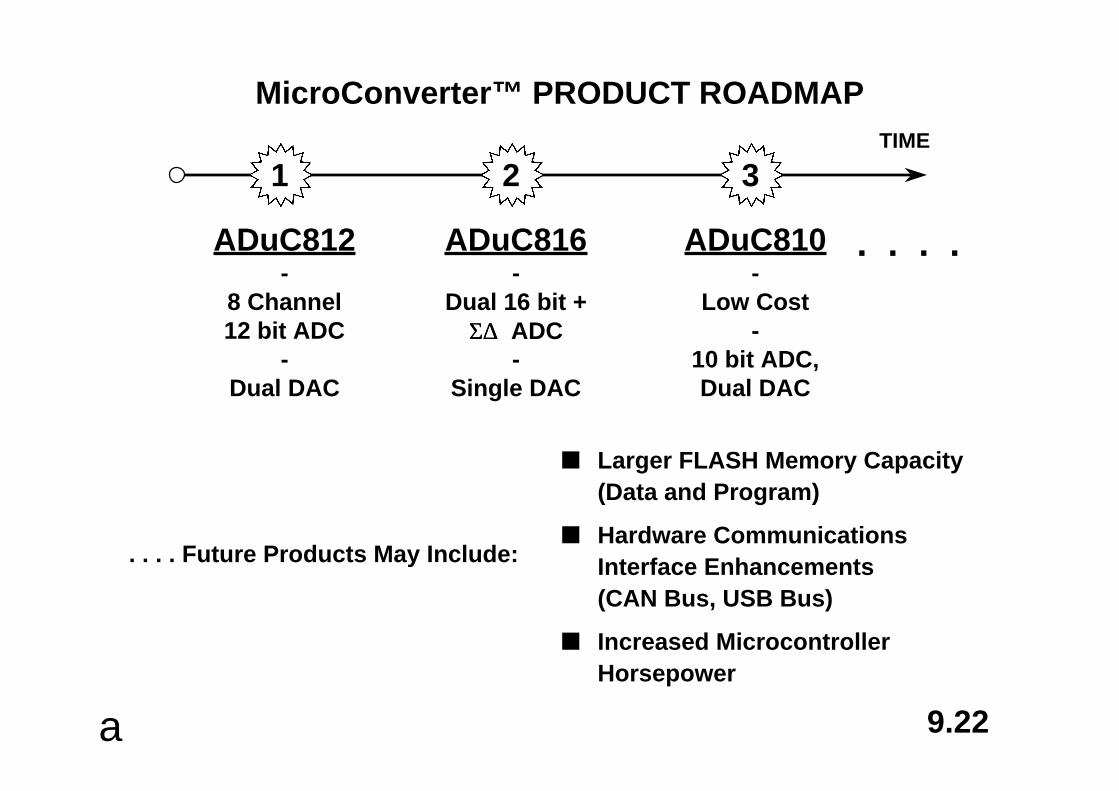
MicroConverter™ PRODUCT ROADMAP
n Larger FLASH Memory Capacity(Data and Program)
n Hardware CommunicationsInterface Enhancements(CAN Bus, USB Bus)
n Increased MicrocontrollerHorsepower
TIME
1
ADuC812-
8 Channel12 bit ADC
-Dual DAC
3
ADuC810-
Low Cost-
10 bit ADC,Dual DAC
2
ADuC816-
Dual 16 bit +Σ∆Σ∆ ADC
-Single DAC
. . . . Future Products May Include:
. . . .