pp read-only memory (rom) keyboard (input) address bus data bus iowc mwtc iorc mrdc read-write...
Post on 21-Dec-2015
251 views
TRANSCRIPT

P
Read-OnlyMemory(ROM)
Keyboard(Input)
Address bus
Data bus
IOWC
MWTC
IORC
MRDC
Read-WriteMemory(RAM)
Printer(Output)

I/O• Any microprocessor need to be interfaced with I/O
devices.
• The I/O address is 16 bit.

Modes of I/O Instructions• Direct I/O – the port address is one of the operands.
– Address must be 00-FFh.• IN AL, 27h
– Data flows through the accumulator • MOV AX, BX
• OUT 26h, AX ; move 16-bit data from AX to port ; 26h (AL to 26h and AH to 27h)
• Indirect I/O – the port address is preloaded into DX– Address can be 0000-FFFFh
• String I/O – allows data to pass directly to or from a memory location.

80x86 I/O InstructionsType Instruction Description
Direct IN AL, port input data to accumulatorIN AX, port port must be in range 00-FFhIN EAX, port
OUT port, AL output data from accumulatorOUT port, AX port must be in range 00-FFhOUT port, EAX
Indirect IN AL, DX input data to accumulatorIN AX, DX port address in DX must be in range 0000-FFFFhIN EAX, DX
OUT DX, AL output data from accumulatorOUT DX, AX port address in DX must be in range 0000-FFFFhOUT DX, EAX
String INSB input data to memory location DS:SI or DS:ESIINSW port address in DX must be in range 0000-FFFFhINSD
OUTSB output data from memory location DS:SI or DS:ESIOUTSW port address in DX must be in range 0000-FFFFhOUTSD
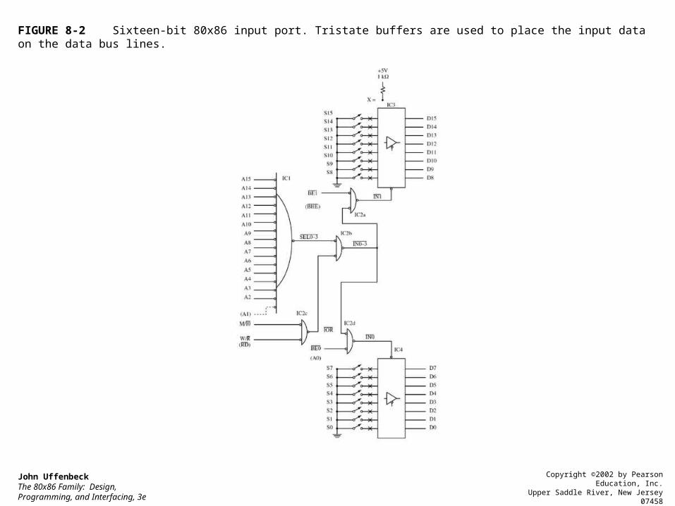
FIGURE 8-2 Sixteen-bit 80x86 input port. Tristate buffers are used to place the input data on the data bus lines.
John UffenbeckThe 80x86 Family: Design, Programming, and Interfacing, 3e
Copyright ©2002 by Pearson Education, Inc.Upper Saddle River, New Jersey 07458
All rights reserved.

FIGURE 8-4 Eight-bit 80x86 output port. Eight latches are required to store the output data.
John UffenbeckThe 80x86 Family: Design, Programming, and Interfacing, 3e
Copyright ©2002 by Pearson Education, Inc.Upper Saddle River, New Jersey 07458
All rights reserved.

FIGURE 8-6 Using device-select pulses to control a relay. An IN AL,0 instruction will turn the relay on; an OUT 0,AL instruction will turn it off.
John UffenbeckThe 80x86 Family: Design, Programming, and Interfacing, 3e
Copyright ©2002 by Pearson Education, Inc.Upper Saddle River, New Jersey 07458
All rights reserved.
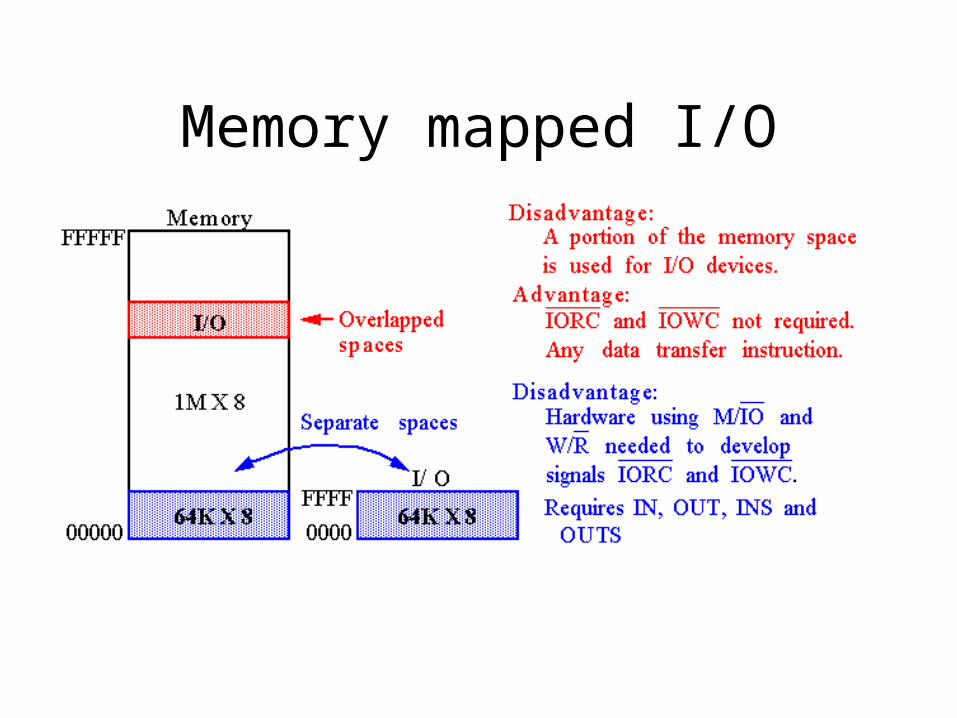
Memory mapped I/O

I/O Map

Programmed I/O

Parallel Printer Interface example

Parallel Printer Interface example

Parallel Printer Interface examplePolling loop
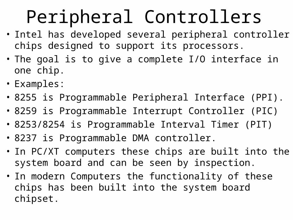
Peripheral Controllers• Intel has developed several peripheral controller chips
designed to support its processors.• The goal is to give a complete I/O interface in one chip. • Examples: • 8255 is Programmable Peripheral Interface (PPI).• 8259 is Programmable Interrupt Controller (PIC)• 8253/8254 is Programmable Interval Timer (PIT)• 8237 is Programmable DMA controller.• In PC/XT computers these chips are built into the system
board and can be seen by inspection.• In modern Computers the functionality of these chips has
been built into the system board chipset.
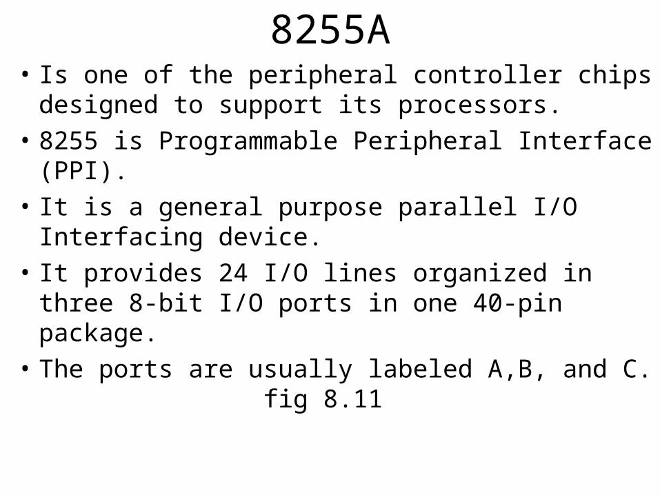
8255A• Is one of the peripheral controller chips designed to
support its processors.
• 8255 is Programmable Peripheral Interface (PPI).
• It is a general purpose parallel I/O Interfacing device.
• It provides 24 I/O lines organized in three 8-bit I/O ports in one 40-pin package.
• The ports are usually labeled A,B, and C. fig 8.11

Size of ports
• Ports A and B can be programmed as an 8-bit input or output port.
• In port C each nipple (four bits) can be programmed separately to be a 4-bit input or output port.
• Only the above size of ports (byte or nipple) can be programmed. For Example, individual bit in a port cannot be programmed.
• However, what make 8254 a versatile devise is its programming modes
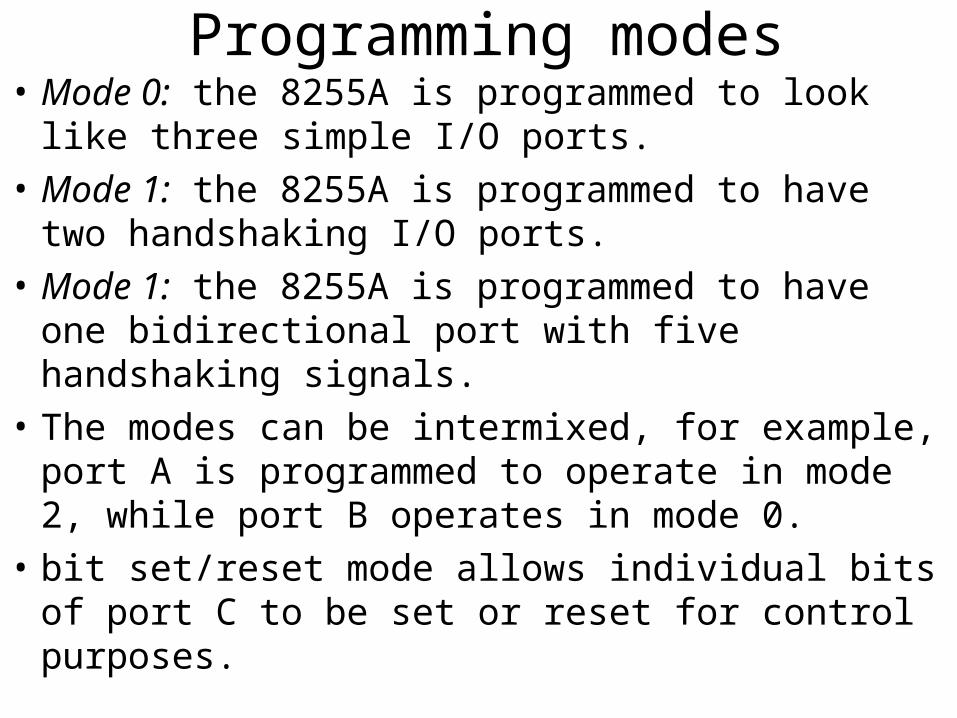
Programming modes• Mode 0: the 8255A is programmed to look like
three simple I/O ports.
• Mode 1: the 8255A is programmed to have two handshaking I/O ports.
• Mode 1: the 8255A is programmed to have one bidirectional port with five handshaking signals.
• The modes can be intermixed, for example, port A is programmed to operate in mode 2, while port B operates in mode 0.
• bit set/reset mode allows individual bits of port C to be set or reset for control purposes.

FIGURE 8-11 8255 programmable peripheral interface (PPI). Twenty-four I/O pins are provided grouped as three 8-bit I/O ports. There is one 8-bit control port. (Courtesy of Intel Corporation.)
John UffenbeckThe 80x86 Family: Design, Programming, and Interfacing, 3e
Copyright ©2002 by Pearson Education, Inc.Upper Saddle River, New Jersey 07458
All rights reserved.

FIGURE 8-12 Interfacing the 8255 to the 386/486 processors. The four PPI ports are mapped to addresses 0, 4, 8, and C.
John UffenbeckThe 80x86 Family: Design, Programming, and Interfacing, 3e
Copyright ©2002 by Pearson Education, Inc.Upper Saddle River, New Jersey 07458
All rights reserved.

8255
A1 A0 RD WR CS Direction0 0 0 1 0 PORT A to data bus0 1 0 1 0 PORT B to data bus1 0 0 1 0 PORT C to data bus
0 0 1 0 0 data bus to PORT A0 1 1 0 0 data bus to PORT B1 0 1 0 0 data bus to PORT C1 1 1 0 0 data bus to control
x x x x 1 data bus in 3rd state1 1 0 1 0 illegal conditionx x 1 1 0 data bus in 3rd state
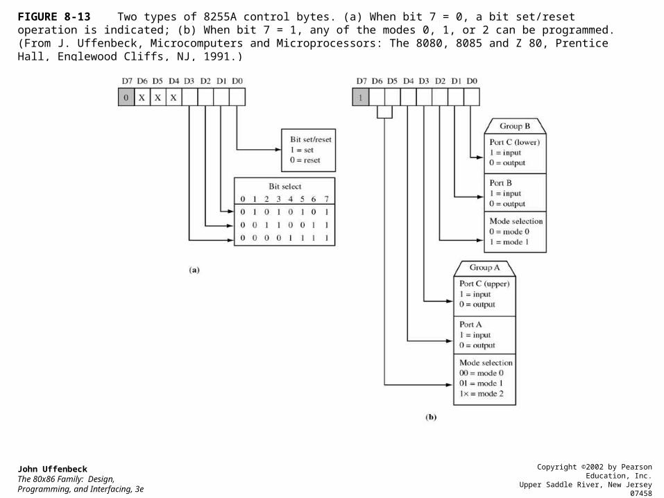
FIGURE 8-13 Two types of 8255A control bytes. (a) When bit 7 = 0, a bit set/reset operation is indicated; (b) When bit 7 = 1, any of the modes 0, 1, or 2 can be programmed. (From J. Uffenbeck, Microcomputers and Microprocessors: The 8080, 8085 and Z 80, Prentice Hall, Englewood Cliffs, NJ, 1991.)
John UffenbeckThe 80x86 Family: Design, Programming, and Interfacing, 3e
Copyright ©2002 by Pearson Education, Inc.Upper Saddle River, New Jersey 07458
All rights reserved.

FIGURE 8-14 Interfacing a 16-key switch matrix to the 8255A (assumed interfaced to the 386/486 circuit shown in Figure 8-12). Port A is programmed as a mode 0 input port and port C (upper) as a mode 0 output port.
John UffenbeckThe 80x86 Family: Design, Programming, and Interfacing, 3e
Copyright ©2002 by Pearson Education, Inc.Upper Saddle River, New Jersey 07458
All rights reserved.
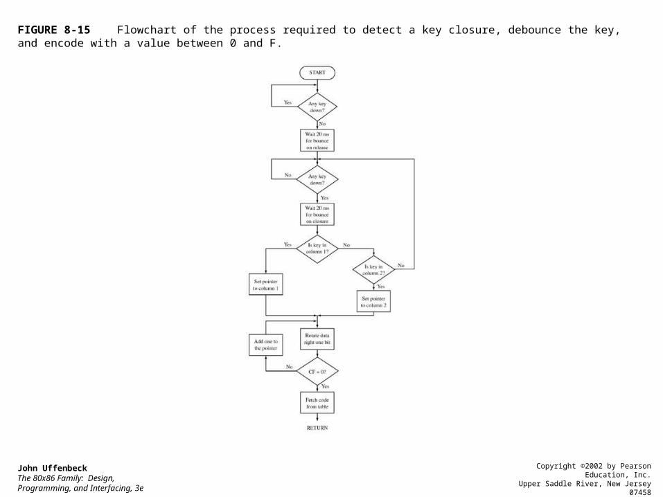
FIGURE 8-15 Flowchart of the process required to detect a key closure, debounce the key, and encode with a value between 0 and F.
John UffenbeckThe 80x86 Family: Design, Programming, and Interfacing, 3e
Copyright ©2002 by Pearson Education, Inc.Upper Saddle River, New Jersey 07458
All rights reserved.

FIGURE 8-17 Block diagram and pin descriptions for the 8254 programmable interval timer. Three separate timers/counters are provided. (Courtesy of Intel Corporation.)
John UffenbeckThe 80x86 Family: Design, Programming, and Interfacing, 3e
Copyright ©2002 by Pearson Education, Inc.Upper Saddle River, New Jersey 07458
All rights reserved.

FIGURE 8-18 Interfacing the 8254 to the three-bus architecture of the 8088 processor. Four I/O ports are required. The port addresses and connections shown correspond to those used in the IBM PC.
John UffenbeckThe 80x86 Family: Design, Programming, and Interfacing, 3e
Copyright ©2002 by Pearson Education, Inc.Upper Saddle River, New Jersey 07458
All rights reserved.

FIGURE 8-19 8254 control word. The standard form is used to specify the operating mode. The counter latch and read-back commands are used when the present count or status is to be read.
John UffenbeckThe 80x86 Family: Design, Programming, and Interfacing, 3e
Copyright ©2002 by Pearson Education, Inc.Upper Saddle River, New Jersey 07458
All rights reserved.

FIGURE 8-22 The 8254 has six different operating modes (mode 0-5). If not shown the GATE (G) input is assumed high to enable the counter.
John UffenbeckThe 80x86 Family: Design, Programming, and Interfacing, 3e
Copyright ©2002 by Pearson Education, Inc.Upper Saddle River, New Jersey 07458
All rights reserved.

• Mode 0: – Event counter (example: timer for interrupt)– When the counter initiated it will start decrement count
from the next T.– Out is low for time of count: (n+1)T.– Gate should be high for the counter to decrement.
• Mode 1: – Hardware initiated counter using Gate (positive pulse).– When the counter initiated it will start decrement count.– Out is low for time of count: nT.

• Mode 2: – The counter will generate a series of continuous pulses.– Out will pulse low for one period low at the end of the
count.– f= clk/n duty cycle=(n-1)/n– Gate should be high.
• Mode 3: – Square wave generator.– Like mode2– Half of the count, out is high and low in the other half.
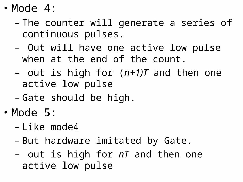
• Mode 4: – The counter will generate a series of continuous pulses.– Out will have one active low pulse when at the end of
the count.– out is high for (n+1)T and then one active low pulse– Gate should be high.
• Mode 5: – Like mode4– But hardware imitated by Gate.– out is high for nT and then one active low pulse