power stage design and implementation of a …etd.lib.metu.edu.tr/upload/12614058/index.pdf ·...
TRANSCRIPT

POWER STAGE DESIGN AND IMPLEMENTATION OF A DEPLOYMENT MECHANISM DRIVER FOR SPACE APPLICATIONS
A THESIS SUBMITTED TO THE GRADUATE SCHOOL OF NATURAL AND APPLIED SCIENCES
OF MIDDLE EAST TECHNICAL UNIVERSITY
BY
BAŞAK GONCA ÖZDEMĐR
IN PARTIAL FULFILLMENT OF THE REQUIREMENTS FOR
THE DEGREE OF MASTER OF SCIENCE IN
ELECTRICAL AND ELECTRONICS ENGINEERING
FEBRUARY 2012

Approval of the thesis:
POWER STAGE DESIGN AND IMPLEMENTATION OF A DEPLOYMENT
MECHANISM DRIVER FOR SPACE APPLICATIONS
submitted by BAŞAK GONCA ÖZDEMĐR in partial fulfillment of the requirements for
the degree of Master of Science in Electrical and Electronics Engineering, Middle East
Technical University by,
Prof. Dr. Canan Özgen __________________
Dean, Graduate School of Natural and Applied Sciences
Prof. Dr. Đsmet Erkmen __________________
Head of Department, Electrical and Electronics Engineering
Prof. Dr. Mirzahan Hızal __________________
Supervisor, Electrical and Electronics Engineering Dept., METU
Examining Committee Members
Prof. Dr. Ahmet Rumeli __________________
Electrical and Electronics Engineering Dept., METU
Prof. Dr. Mirzahan Hızal __________________
Electrical and Electronics Engineering Dept., METU
Prof. Dr. Muammer Ermiş __________________
Electrical and Electronics Engineering Dept., METU
Prof. Dr. Osman Sevaioğlu __________________
Electrical and Electronics Engineering Dept., METU
M.Sc. Hasan Özkaya __________________
TÜBĐTAK UZAY
Date: 10.02.2012

iii
I hereby declare that all information in this document has been obtained and presented in accordance with academic rules and ethical conduct. I also declare that, as required by these rules and conduct, I have fully cited and referenced all material and results that are not original to this work.
Name, Last name : Başak Gonca Özdemir
Signature :

iv
ABSTRACT
POWER STAGE DESIGN AND IMPLEMENTATION OF A DEPLOYMENT
MECHANISM DRIVER FOR SPACE APPLICATIONS
Özdemir, Başak Gonca
M.Sc., Department of Electrical and Electronics Engineering
Supervisor: Prof. Dr. Mirzahan Hızal
February 2012, 136 pages
With the developments in space technology, the capabilities of spacecrafts have been
increased considerably which in turn have entailed the development of more efficient
spacecrafts in terms of cost, mass, size and power. One way to achieve such a development
is the replacement of body mounted appendages with the deployable ones, which greatly
reduces the size, mass and cost of the spacecraft especially when large appendages are
considered. In order to obtain these deployable structures, deployment mechanisms and
deployment mechanism drivers are used. A deployment mechanism is a combination of
electrical and/or mechanical structures which hold the appendages in the stowed position
before launch and deploys them after the launch with the power and commands supplied by
the deployment mechanism driver. This necessary power of the deployment mechanism
driver is produced by the Power Stage of the deployment mechanism driver and the
necessary commands required by the deployment mechanism are supplied by the Control
Stage of the deployment mechanism driver. In this thesis, the power stage of a deployment
mechanism driver will be designed and implemented taking into account of the
requirements for Low Earth Orbit Satellites such as temperature tolerance, reliability and
radiation limits. In order to acquire a cost, mass and size efficient Power Stage, different
deployment mechanism topologies will be studied and the most convenient one among
these topologies will be chosen as the deployment mechanism driver load and the design
will be performed accordingly.
Keywords: deployment mechanism driver, space applications.

v
ÖZ
UZAY UYGULAMALARINDA KULLANILAN BĐR AÇILMA MEKANĐZMASI
SÜRÜCÜSÜNÜN GÜÇ AŞAMASININ TASARIMI VE GERÇEKLEŞTĐRĐLMESĐ
Özdemir, Başak Gonca
Yüksek Lisans, Elektrik-Elektronik Mühendisliği Bölümü
Tez Yöneticisi: Prof. Dr. Mirzahan Hızal
Şubat 2012, 136 pages
Uzay teknolojisindeki gelişmeler ile birlikte uzay araçlarının yetenekleri önemli ölçüde
artmış, bu durum da maliyet, ağırlık, boyut ve güç açısından daha verimli uzay araçlarının
geliştirilmesini gerektirmiştir. Bu gelişmeyi sağlayan yollardan birisi, gövdeye monteli
uzay aracı uzantı modüllerinin açılabilir olanlar ile değiştirilmesidir. Bu sayede özellikle
büyük modüller söz konusu olduğunda boyut, ağırlık ve maliyet önemli ölçüde
azalmaktadır. Açılabilir modüllerin elde edilmesi amacıyla açılma mekanizmaları ve açılma
mekanizması sürücüleri kullanılmaktadır. Elektriksel ve/veya mekanik yapıların birleşimi
olan açılma mekanizması, fırlatma öncesinde ilgili modülleri kapalı konumda tutan ve
fırlatma sonrasında açılma mekanizması sürücüsü tarafından gönderilen elektriksel güç ve
kontrol komutları doğrultusunda bu modülleri açan bir mekanizmadır. Açılma mekanizması
tarafından ihtiyaç duyulan bu elektriksel güç, açılma mekanizması sürücüsünün Güç
Aşaması tarafından üretilmekte ve açılma mekanisması tarafından ihtiyaç duyulan kontrol
komutları da açılma mekanizması sürücüsünün Kontrol Aşaması tarafından sağlanmaktadır.
Bu tezde, alçak irtifa uyduları için belirlenmiş olan sıcaklık dayanımı, güvenilirlik ve
radyasyon limiti gibi gereksinimler göz önünde bulundurularak bir açılma mekanizması
sürücüsünün Güç Aşaması tasarlanacak ve gerçekleştirilecektir. Maliyet, ağırlık ve boyut
açısından verimli bir Güç Aşaması elde edebilmek amacıyla değişik açılma mekanizmaları
topolojileri incelenecek ve bu topolojiler arasından en uygun olanı açılma mekanizması
sürücüsü yükü olarak seçilerek tasarım bu doğrultuda yapılacaktır.
Anahtar Kelimeler: açılma mekanizması sürücüsü, uzay uygulamaları

vi
To My Family

vii
ACKNOWLEDGMENTS
I would like to express my gratitude and deep appreciation to my supervisor Prof. Dr.
Mirzahan Hızal for his guidance, support and valuable suggestions.
I would also like to express my thanks to my parents Nebahat Özdemir and Ekrem
Özdemir, my sister Sevda Özdemir Aksoy, my nephew Hasan Poyraz Aksoy and my
brother in law Arif Yavuz Aksoy.
Finally, I would like to thank my colleagues at TÜBĐTAK UZAY, especially Power
Conversion and Analogue Systems Group Leader; Hasan Özkaya, for their help and support
during my studies.

viii
TABLE OF CONTENTS
ABSTRACT ................................................................................................................... IV
ÖZ .................................................................................................................................... V
ACKNOWLEDGMENTS .............................................................................................. VII
TABLE OF CONTENTS .............................................................................................. VIII
LIST OF TABLES .......................................................................................................... XI
LIST OF FIGURES ....................................................................................................... XII
CHAPTERS .......................................................................................................................1
1. INTRODUCTION ..................................................................................................1
1.1 Related Work .................................................................................................7
1.1.1 Deployment Mechanism Actuators ......................................................7
1.1.2 DeploymentMechanismDriver ........................................................... 11
1.2 Scope ........................................................................................................... 13
1.3 Outline ......................................................................................................... 13
2. POWER STAGE OF A DEPLOYMENT MECHANISM DRIVER ...................... 15
2.1 Selection of the Deployment Mechanism Actuator ....................................... 17
2.2 Configuration of the Deployment Mechanism Power Stage .......................... 19
2.3 Voltage Regulator ........................................................................................ 21
2.3.1 Linear Regulators ............................................................................. 22
2.3.2 Switch Mode Regulators ................................................................... 24
2.4 Step-Down (Buck) Converter ....................................................................... 27
2.4.1 Basic Logic of the Power Stage ........................................................ 28
2.4.2 Conduction Modes of the Buck Converter ........................................ 30
2.4.3 Buck Converter Operation Analysis .................................................. 32

ix
2.4.4 Selection of the Components in the Power Stage ............................... 34
2.4.4.1 Inductor ............................................................................ 34
2.4.4.2 Capacitor ........................................................................... 38
2.4.4.3 Power Switch .................................................................... 42
2.4.4.4 Diode ................................................................................ 44
2.5 Control Methods in Step-Down (Buck) Converter ........................................ 46
2.5.1 Control Stage of the Buck Converter................................................. 46
2.5.2 Control Methods ............................................................................... 49
2.5.2.1 Voltage Mode Control ....................................................... 49
2.5.2.2 Current Mode Control ....................................................... 50
2.5.2.3 Types of Current Mode Control ......................................... 52
2.5.3 Average Current Mode Control ......................................................... 56
2.5.3.1 State Space Averaged Model of the Buck Converter with
. ACMC .............................................................................. 57
2.5.3.2 Design of the Current Compensator .................................... 60
2.5.3.3 Design of the Voltage Loop ................................................ 62
3. PROPOSED SYSTEM ......................................................................................... 65
3.1 Introduction ................................................................................................. 65
3.2 Hardware Implementation ............................................................................ 66
3.2.1 Implementation Details of the Buck Converter .................................. 66
3.2.2 Implementation Details of Control Loop ........................................... 73
3.2.3 Implementation Details of the ACMC IC .......................................... 78
3.2.3.1 General Considerations...................................................... 79
3.2.3.2 Adjusting the Oscillator ..................................................... 81
3.2.3.3 Average Current Mode Control Block ............................... 83
3.2.3.4 Voltage Amplifier ............................................................. 83
3.2.3.5 Current Sense Amplifier .................................................... 84
3.2.3.6 Current Amplifier and PWM ............................................. 86

x
3.2.3.7 Soft Starting of UC3886D .................................................. 87
3.2.3.8 Driving the MOSFET Switch with UC3886D ..................... 88
4. EXPERIMENTS .................................................................................................. 92
4.1 Simulations .................................................................................................. 92
4.2 Test Procedure and Test Results ................................................................. 100
4.2.1 Power Stage Tests .......................................................................... 102
4.2.2 Control Stage Tests......................................................................... 105
4.2.3 Overall System Tests ...................................................................... 107
5. CONCLUSIONS ................................................................................................ 115
5.1 Summary .................................................................................................. 115
5.2 Discussions ............................................................................................... 116
5.3 Future Work .............................................................................................. 118
REFERENCES .............................................................................................................. 120
APPENDICES
A. BASICS OF DEPLOYMENT MECHANISM ACTUATORS............................. 125
B. INPUT CURRENT LIMITER ............................................................................ 133

xi
LIST OF TABLES
TABLES
Table 1 Advantages and Disadvantages of Commonly Used Actuators ............................. 18
Table 2 Thermal Knife (MHRM) Electrical Characteristics .............................................. 20
Table 3 Commonly Used Switching Regulator Topologies ............................................... 25
Table 4 Buck Converter Parameters ................................................................................. 67
Table 5 7445920 POWER-CHOKE WE-PD 3 Properties ................................................. 68
Table 6 CTC21E Properties .............................................................................................. 70
Table 7 Si4484EY Electrical Characteristics [69] ............................................................ 71
Table 8 Test Equipments ................................................................................................ 100
Table 9 Electrical Characteristics of Some Commonly Used Actuators ........................... 129

xii
LIST OF FIGURES
FIGURES
Figure 1 Deployment Mechanism Driver Main Blocks ..................................................... 15
Figure 2 Power Stage Main Blocks ................................................................................... 20
Figure 3 Linear Regulator ................................................................................................ 22
Figure 4 Series Linear Regulator ...................................................................................... 22
Figure 5 Linear Regulator with Feedback ......................................................................... 23
Figure 6 Switch Mode Regulator ...................................................................................... 24
Figure 7 Buck Converter Power Stage .............................................................................. 27
Figure 8 Buck Converter Basic Logic ............................................................................... 28
Figure 9 ON State ............................................................................................................ 29
Figure 10 OFF State ......................................................................................................... 29
Figure 11 Waveform for Vs.............................................................................................. 30
Figure 12 Waveform for VL ............................................................................................. 30
Figure 13 Waveform for Vout .......................................................................................... 30
Figure 14 Waveforms in Continuous Conduction Mode.................................................... 31
Figure 15 Waveforms in discontinuous conduction mode ................................................. 32
Figure 16 Inductor Voltage VL and Inductor Current IL during CCM Operation ................. 33
Figure 17 Inductor Current Waveform .............................................................................. 35
Figure 18 Optimization Chart for Setting “r” [11] ............................................................. 38
Figure 19 Buck Converter Output Voltage Ripple ............................................................ 39
Figure 20 Control Stage of the Buck Converter ................................................................ 46
Figure 21 PWM Pulses ..................................................................................................... 47
Figure 22 Voltage Mode Control ...................................................................................... 49
Figure 23 Current Mode Control ...................................................................................... 50
Figure 24 Slope Compensation in Current Mode Control .................................................. 51
Figure 25 For D < 50%, disturbances die out with each cycle ........................................... 51
Figure 26 For D > 50%, disturbances grow with each cycle and sub-harmonic oscillations
are observed ........................................................................................................ 52
Figure 27 With Slope Compensation Disturbances Die Out with each cycle and for any D52

xiii
Figure 28 Peak Current Mode Control .............................................................................. 53
Figure 29 Valley Current Mode Control ........................................................................... 53
Figure 30 Average Current Mode Control ........................................................................ 56
Figure 31 Block Diagram of State Space Averaged Converter Model [62] ........................ 57
Figure 32 Current Loop Block Diagram ........................................................................... 58
Figure 33 Current Compensator........................................................................................ 60
Figure 34 PWM Pulses and Control Voltage Waveforms .................................................. 62
Figure 35 Voltage Controller ............................................................................................ 63
Figure 36 Block Diagram of the Proposed System ............................................................ 65
Figure 37 Output Characteristics [69] ............................................................................... 72
Figure 38 On-Resistance vs. Drain Current [69] ............................................................... 72
Figure 39 Bode Plot for Tc(s), Gca(s) and Gpcl(s) ............................................................ 76
Figure 40 Bode Plot for Toc(s) ......................................................................................... 77
Figure 41 Bode Plot for Toc(s), Tv(s) and Gva(s) ............................................................. 78
Figure 42 Block Diagram of UC3886 [70] ........................................................................ 79
Figure 43 Power Distribution Blocks within UC3886 [70] ................................................ 80
Figure 44 UC3886 Oscillator Waveform [24] ................................................................... 81
Figure 45 UC3886 ACMC Blocks [24] ............................................................................ 83
Figure 46 Setting VCOMMAND [24] .............................................................................. 84
Figure 47 Current Sense Amplifer Configuration [24] ...................................................... 85
Figure 48 Current Sense Amplifer with Voltage Divider Network .................................... 85
Figure 49 Current Compensator, Voltage Controller and PWM configuration ................... 86
Figure 50 Soft Start of UC3886 [24] ................................................................................. 87
Figure 51 Bootstrap Driving ............................................................................................. 89
Figure 52 Buck Converter Schematic ............................................................................... 93
Figure 53 Vout for Vin=28V and Rout=20Ohm ................................................................... 93
Figure 54 Settling Time for Vout for Vin=28V and Rout=20Ohm ........................................ 94
Figure 55 Output Voltage Ripple ...................................................................................... 94
Figure 56 PWM Output (R8.V) ........................................................................................ 95
Figure 57 Voltage Waveforms for SW1 and Dfw via VM2.V (Green Line) and VM3.V(Red
Line) respectively ................................................................................................ 95
Figure 58 Output Current (Red Line) during Output Load Change (Blue Line) ................. 96
Figure 59 Zoomed View for Output Current (Red Line) during Output Load Change (Blue
Line) ................................................................................................................... 97

xiv
Figure 60 Input Voltage Change (Blue Line) and Output Voltage Response (Red Line) .... 98
Figure 61 Input Voltage Change from 28V to 25V (Blue Line) and Output Voltage
Response (Red Line) ........................................................................................... 98
Figure 62 Input Voltage Change from 25V to 33V (Blue Line) and Output Voltage
Response (Red Line) ........................................................................................... 99
Figure 63 Output Voltage Ripple at Vin=25V ................................................................... 99
Figure 64 Output Voltage Ripple at Vin=33V ................................................................. 100
Figure 65 Experimental Test Set-up ............................................................................... 101
Figure 66 Power Stage Circuitry Top and Bottom Views Respectively ........................... 101
Figure 67 PWM Pulses (CH1-Yellow), LO (CH2-Blue) and HO (CH3-Purple) Outputs . 102
Figure 68 LO (CH2-Blue) and HO (CH3-Purple) Outputs with Rgate=12Ohm ................. 103
Figure 69 Closer View for LO (CH2-Blue) and HO (CH3-Purple) Outputs with
Rgate=12Ohm...................................................................................................... 103
Figure 70 Freewheeling Diode Waveform ...................................................................... 104
Figure 71 Output Voltage Waveform (20V) for Vin=28V ............................................... 104
Figure 72 Sawtooth Voltage Waveform (CH3-Purple) .................................................... 105
Figure 73 PWM pulses (CH4-Green) for VSENSE=1.922V ........................................... 106
Figure 74 PWM pulses (CH4-Green) for VSENSE=1.945V ........................................... 106
Figure 75 PWM pulses (CH4-Green) for VSENSE=1.963V ........................................... 107
Figure 76 PWM pulses (CH4-Green) for VSENSE=1.972V ........................................... 107
Figure 77 Output Voltage for Vin=28V and Rout=200Ohm ............................................ 108
Figure 78 PWM waveform (CH4-Green) for Vin=28V and Vout=20Ohm ...................... 109
Figure 79 Zoomed View for the Ringing in the PWM waveform (CH4-Green) ............... 109
Figure 80 Waveform of the Freewheeling Diode (CH4-Green) ....................................... 110
Figure 81 Zoomed View for the Ringing in the Freewheeling Diode (CH4-Green) ......... 110
Figure 82 Delay between High Side (CH4-Green) and Low Side (CH1-Yellow) Switch
Drive Pulses ...................................................................................................... 111
Figure 83 Delay between Low Side (CH1-Yellow) and High Side (CH4-Green) Switch
Drive Pulses ...................................................................................................... 111
Figure 84 Output Voltage (CH3-Purple) Rise from 0V to 20V and Output Current (CH1-
Yellow) Rise from 0A to 200mA ....................................................................... 112
Figure 85 Output Voltage (CH3-Purple) Rise from and Output Current (CH1-Yellow) Rise
.......................................................................................................................... 112

xv
Figure 86 Output Voltage (CH4-Green) and Current (CH1-Yellow) Waveforms for Rout
Change from 200Ohm to 20Ohm ....................................................................... 113
Figure 87 Output Voltage (CH3-Purple) and Current Waveforms (CH1-Yellow) for Rout
Change from 22Ohm to 12Ohm ......................................................................... 114
Figure 88 Pyrotechnic Cutter .......................................................................................... 126
Figure 89 HOP Pin Pusher [20] ...................................................................................... 126
Figure 90 SMA Hinge [45, 55] ....................................................................................... 127
Figure 91 Thermal Knife ................................................................................................ 128
Figure 92 Fold-back Current Limiting ............................................................................ 133
Figure 93 Fold-back Current Limiter with External Turn On/Off Control ....................... 134
Figure 94 Foldback Current Limiter Top and Bottom View ............................................ 135
Figure 95 MOSFET Switch Turn Off during an overload ............................................... 135

1
CHAPTER 1
1. INTRODUCTION
Following the launch of first artificial satellite, Sputnik 1, by the Soviet Union in 1957,
there has been a great competition and progress in the field of space applications. Space
applications mainly consist of artificial satellites, space planes, space stations and several of
other structures which can be named under a general term, “spacecraft”. Each spacecraft is
designed according to its mission. General mission types can be given as navigation,
communications, meteorology, earth observation, planetary exploration and human and
cargo transportation. Within time and with the developments in sciences that take part in
these applications, capability of spacecrafts has greatly increased which in turn has resulted
in an increase in the power need, cost and mass of the spacecrafts. In order to meet the
power demand of the spacecrafts via the solar panels, the solar array area has been
increased. However, in the case of the body mounted solar panels, this increment is limited
to the total outer area of the spacecraft that can be used for solar panels. Even if the whole
area is covered with high efficiency solar cells, power demand may be met but in this case
the spacecraft cost will increase dramatically. Also, as the capability of the spacecrafts has
increased, several other devices have been developed and integrated onto the spacecraft
depending on the mission type. Some of these devices are mounted directly on the outer
surface of the spacecrafts which causes a great increase in the volume of the spacecraft. In
addition to these, it is possible that these devices can be damaged easily during the launch.
So, either due to the bigger and larger solar panels or due to the mounting of other devices
such as antennas, magnetometer booms, etc, the volume that the spacecraft covers in the
launch vehicle also rises. As a result, launch vehicle expanses which can be the biggest
amount of the total project price in some cases, increases dramatically. In order to keep the
volume and mass of the spacecraft in acceptable levels and decrease the cost, deployment
mechanisms have been developed.
CHAPTERS

2
Deployment mechanisms are used for keeping the devices that cover big volumes stowed
during the launch and releasing them during the different phases of the mission. Some of
these devices are solar panels, antennas, magnetometer booms, solar sail booms, etc. As
mentioned above, with the use of the deployment mechanisms it is possible to use single
panel flip out solar panel configurations or multi-panel deployable solar panel systems
instead of the body mounted solar panels, hence larger solar panel area is achieved after the
deployment. Also, this helps to reduce the cost of the solar panels by using cheaper low
efficiency solar cells over a large surface which in turn meets the required power demand
with decreased cost. And by the use of the deployment mechanisms, other devices such as
antennas or magnetometer booms are protected against the crashes during the launch and
the volume that they occupy within the launch vehicle and hence the launch expanses are
reduced.
Stowing of the deployable structures before the launch and releasing them when required,
as mentioned in the above, can be named as the hold down and release operation. In order
to perform hold down and release operation, deployment mechanisms use actuators.
Deployment mechanism actuators are electrically activated devices which performs
deployment by giving initial movement to the mechanical structure of the deployment
mechanism such as the springs, hinges etc. The initial movement can be generated by either
cutting or releasing the hold down interface which holds the deployable structure in the
stowed position. Although deployment mechanism actuators have various types and each
day new actuators are introduced to the market, commonly used actuators can be classified
as explosive actuators (pyrotechnic actuators) and the non explosive actuators. Explosive
actuators have been widely used since 1950s due to their capability to produce high output
force/power within a small volume [39]. However, they produce high mechanical and
functional shocks which may result in failure of electronic subsystems close to the shock
load source. Also, they are susceptible to unintentional functioning due to in rush currents
since they contain explosive compounds. Due to their high risk level which have been
published in several documents by NASA and ESA [20], non explosive actuator concept
has gained importance. Non explosive actuators usually depend on heating of different
materials to produce force by volumetric-pressure change (High Output Paraffin Actuators-
HOP Actuators), to perform the movement by shape change of memory alloys (Shape
Memory Alloy Actuators– SMA Actuators) or to cut and release the hold down cable by
heater elements (Thermal Knife Actuator). Although non explosive actuators have low
shock profiles and safer due to not using any explosives, depending on their operational

3
requirements they have different advantages and disadvantages. HOP actuators and SMA
actuators require high current ratings up to 10A in order to be activated [20]. Also their
operational temperature range is narrow when compared with the thermal knife structures.
HOP actuators need extra safety circuitries for power termination due to high pressure
produced in them. Otherwise, actuator itself and the nearby circuitries can be destroyed.
SMA actuators on the other hand contain the risk of forgetfulness since their operation is
based on shape memory of the alloys. Also they contribute to EMI due to high input current
pulses. Thermal knife actuators do not have any of the risks mentioned above since their
operation depends on thermal degradation of the hold down cable by heating ceramic
blades with a lower current rating. Also, thermal knife actuators are insensitive to
disturbances so there is no risk of unintentional release of the actuator. Although thermal
knife is not suitable for simultaneous and instantaneous deployment operations, it is the
prominent actuator type when safety, reliability and cost of the overall system are
considered.
In addition to actuator, each deployment mechanism needs a driver to supply necessary
power to the actuator and to control its operation. Power can be supplied to the actuators
either from the battery block or from the power distribution switches of the power
subsystem. Battery block is the main energy supply of the spacecraft in addition to the solar
panels. It is charged by the solar panels and supplies necessary power to whole spacecraft
during eclipse periods where solar panels do not produce power. Battery block produces
unregulated power usually in the range of 28V±5V DC. Power produced by the battery
block is not directly fed to subsystems or circuitries; it is distributed by the 28V Power
Distribution Switches as the spacecraft bus voltage. These switches can be used to switch
on and switch off a subsystem or module by sending necessary telecommands; hence a
controlled power on sequence is achieved. Also, these switches have protection function
which is obtained by automatic switch off function in case of a overload or short circuit.
Although actuators use different operating voltages and current ratings, depending on their
power need and the output force that is required, main rule for the input supply of the
actuator to be a well regulated DC supply which produces controllable DC voltage and
current within the limits of the actuator. So, deployment mechanism driver includes a
Power Stage which regulates either the battery block power or the power distribution switch
power according to the input voltage and current demand of the actuator. Although it is
simpler to directly feed an actuator through the power distribution switches or through the
battery block in terms of additional mass, volume, complexity and work load that a

4
specially designed power stage brings on the system, such a power stage for the deployment
mechanism driver is needed in order to guarantee a safe operation and obtain the different
voltage and current ranges that the actuators require. The need for a specially designed
deployment mechanism power stage has many reasons.
First of all, for the actuators which depend on heating for a certain duration to operate (such
as the non explosive actuators), variation of the supply voltage causes the heating power to
change too. Variations in the heating power cause the actuator operation to deviate from the
expected. This deviation can result in a shorter/longer operation duration which creates a
risk for the operations where timing is critical such as the simultaneous operations. Also,
variations in the input power cause the lives of the actuators to shorten. Even if the
actuators are supposed to be used only once in the orbit, several on ground functional tests
have to performed with the actual driver of the battery before the launch. And due to
constantly changing voltage and current levels during these tests wear out of the actuators
and its supply becomes faster which endangers the operation of the actuators in the orbit.
Apart from the timing and lifetime constraints, feeding the actuators with a variable supply
can cause malfunctioning of the actuators. HOP actuators, for example, produces high
pressure as a result of heating. In case poorly controlled power is supplied to HOP
Actuators, it becomes difficult to control the pressure build up and in turn the possible
damages due the pressure. Same assumption is also true for other actuators where too long
heating with too high power can cause overheating of the constituting elements of the
actuator and as a result damage or destroy them.
Secondly, changes in the supply current or voltage may cause a decrease in the operation
capability of the actuators and the interface elements such as the connectors or the wires.
Exceeding the limits or supplying them with variable voltage or current levels cause these
elements to derate or to be damaged. Derating the capability of the interface elements may
result in open or short circuit conditions either case of which is highly risky. In case of an
open circuit due to the derating or wear out of the connectors or wires, actuators cannot be
supplied and hence deployment cannot be carried out. As a result, critical structures such as
the solar panels are not deployed and so the spacecraft continues to operate only until the
stored energy of the spacecraft is finished since it is not possible to charge the batteries
enough if the solar panels are not deployed. In case of a short circuit on the connecting
elements, the current track will be damaged and again it will not be possible to supply the

5
actuators or more worse than actuators will be supplied well above their limits resulting in
damage on themselves, on the nearby circuitries and even on the critical subsystems.
Another possible consequence of supplying the actuators with a poorly regulated supply
with varying voltage and current levels are the undervoltage or undercurrent cases.
Supplying an actuator below its limits prolongs the deployment duration which is not
acceptable for operations such as simultaneous or instantaneous operations where timing
has great importance. Far worse than this, less voltage or current can cause an uncompleted
deployment operation For example, in the case of thermal knife, less power causes the
heater knives to be heated less and as a result melting of the hold down cable may not
completed. Even worse, trying to melt the hold down cable below the required temperature
may result in gluing of the hold down cable on to the heaters. If this situation occurs during
the mission, it may not be possible to continue and complete the deployment operation and
so the spacecraft may be lost due to losing critical appendages. If this situation is
encountered during the ground tests, heater blades have to be changed with new ones. The
number of changes is limited to increase the reliability of the actuator and hence if these
limits are exceeded, thermal knife becomes completely unusable and have to be replaced
totally with a new one which brings additional cost. The situation is same with the other
actuators too. In case deployment is uncompleted and critical appendages such as solar
panels or antennas are not deployed spacecraft may be lost either due to power loss or due
to communication loss.
Depending on the above discussions, although using battery block directly as the power
stage of the deployment mechanism driver without specially designed additional regulator
and protection circuitries eliminates the additional weight, volume and cost and complexity
that such a circuitry brings, it is obvious that direct feeding from battery block increases the
risk of malfunctioning or damage of the actuators and hence the risk of unsuccessful
deployment or loss of mission to an unacceptable level. In case of direct feeding of the
actuators without an additional deployment mechanism driver power stage by using 28V
Power Distribution Switches a relatively controlled power on-off sequence can be obtained.
Hence additional protection circuitries may be eliminated. However, in case of using
pyrotechnical or SMA actuators which require very high current ratings as high as 10A
makes the power input to these actuators greatly increase. Such an increase in the input
power, even for a short duration, brings the risk of malfunctioning or short circuiting of the
Power Distribution Switches due to heat dissipation. Since Power Distribution Switches

6
which feed the whole spacecraft systems are located in the same module together, taking
such a risk endangers the whole spacecraft bus and so the systems. So, even if usage of a
separate regulator may be eliminated with direct feeding of actuators through Power
Distribution Switches, additional line and load protection circuitries must be included to
increase the reliability and to guarantee a safe operation. Also, if any actuator with input
voltage range different from 28V is to be used, using a regulator circuitry is a must for a
direct feeding either with the battery block or with the Power Distribution Switches.
As a result, a specially designed and highly reliable Power Stage with an efficient and well
controlled regulator shall be designed which supplies a well regulated DC voltage and
current for the actuators in order to eliminate or decrease the highly possible
failure/malfunctioning cases due to using battery blocks or the power distribution switches
as the power stage itself as explained above. Designing such a power stage increases the
reliability and decreases the risk of unsuccessful deployment phases, damage of the
actuators themselves or the nearby systems due to uncontrolled power input. Usage of
different external safety circuitries in addition to the power stage itself, are also used in
order to increase the reliability level even higher, enable redundancy and hence eliminate
the risk of single point of failure. These external circuitries include input current limiters
between the input of the power stage of the deployment mechanism driver and battery
block/spacecraft power bus, and output activation switches between the deployment
mechanism actuators and the power stage output. Using input current limiter not only
protect the battery or the spacecraft power bus in case of a failure but also disconnect the
power stage and hence the actuators from power. In the same way, output activation
switches can be used to increase the control on activation of the deployment mechanism
actuators and hence in case of a failure, actuators and the power stage are supposed to be
protected and any failure on system level are avoided.
Hence, using a specially designed power stage for the deployment mechanism driver with a
controllable output power provides protection for not only the actuators or the deployment
itself but also for the whole spacecraft and the mission by decreasing the risk level and
increasing the reliability. In order to increase reliability and safety even more, in addition to
power stage, different protection circuitries for the spacecraft power bus and the
deployment mechanism actuators can also be used.

7
1.1 Related Work
The main concern that determines the design of a deployment mechanism and in turn the
deployment mechanism driver is the mission of the spacecraft. According to the mission
requirements, the appendages that will be deployed by the deployment mechanism gain
special characteristics. For example, in the case of the solar panels, the power need of the
spacecraft is one of the determinant factors. According to this need, the size, weight and
configuration (body mounted, single panel flip out or multi panel deployable systems) of
the solar panels are determined. Then, considering the orbit that the spacecraft will be
launched to and the launch vehicle characteristics, other factors such as the required
duration for the deployment, shock load limits, radiation and temperature levels are
criticized. Taking into account of all the related factors, deployment mechanisms and
actuator mechanisms are evaluated. Throughout this evaluation, different deployment
schemes including the configuration of the actuator mechanisms with the necessary
mechanical elements such as coil or torsion springs, hinges, support brackets etc. should be
criticized. Also, deployment mechanism driver choices are considered in terms of
complexity, controllability, reliability, mass, etc. since each actuator mechanism has special
electrical supply characteristics. Later, a suitable actuator mechanism or an initial release
mechanism [19] and a suitable deployment mechanism driver configuration are chosen
according to the above mentioned requirements.
In order to evaluate the deployment mechanism drivers and the power stage related with
them, first of all most commonly used deployment mechanism actuators will be reviewed in
Subsection 1.2.1. Afterwards, literature survey on the deployment mechanism drivers and
their power stage will be given in Subsection 1.2.2.
1.1.1 Deployment Mechanism Actuators
As can be understood from its name, actuator mechanisms are used for initiating the
deployment of the appendage and deployment mechanism drivers are designed according to
the actuator type chosen. Usage of deployment mechanisms and so the actuators go back to
late 1950s. One type of such an actuator is the “Pyrotechnic Actuators”. Pyrotechnic
actuators are the devices which perform several mechanical functions such as switching,
cutting, releasing and ignition by the utilization of self contained energy sources which are
namely explosives, propellants and pyrotechnic compositions [20]. Pyrotechnic devices
have been used in many space programs and have an old history which goes back to the

8
Project Mercury, which was the first human spaceflight program of the United States
conducted from 1959 to 1963. In the Mercury Project a total of 46 pyrotechnic devices
were used [39]. In the Apollo Program which ran after Mercury and Gemini projects by
NASA between 1961 and 1972, 314 pyrotechnic devices were used [39]. Mars Pathfinder
of NASA, launched in December 1996, used 42 pyro devices during its mission for
atmospheric entry and landing [35]. In the twin GRACE (Gravity Recovery and Climate
Experiment) Satellites which have been launched on March 2002 as a joint mission of
NASA and German Space Agency, pyrotechnic actuators were used in addition to pusher
drives in order to perform separation of the satellites from the launch vehicle [33]. Despite
of its advantages such as high output power, mass and volume efficiency and instantaneous
operation, the main drawbacks for the pyrotechnical devices are the high levels of explosive
(pyroshocks) and mechanical shocks which may result in failure in the electronic
components, creation of vibration on the spacecraft structure and endangerment of other
spacecrafts during the launch phase due to the possibility of unintentional firing. Although
there is not enough data on the failure of electronic components/systems due to pyroshocks,
C.J. Moening [20] mentions in his paper named “Pyrotechnic Shock Flight Failures” in
1985 that through 1984, in approximately 600 launches, 83 pyroshock related failures had
occurred over 50 of which had resulted in loss of mission. In 1988, L.J. Bement, conducted
a survey about pyrotechnic device failures on NASA centers, and in his paper named
"Pyrotechnic System Failures: Causes and Prevention” it is mentioned that throughout a
period of 23 years, 84 failures occurred due to pyrotechnics [40]. Of the 84 failures, 12 of
which occurred during the flight, approximately 35 (42% of the 84 failures) of them were
due to the lack of understanding of the pyrotechnic devices; 24 of the failures
(approximately 28%) were due to inadequate design and misapplication of the related
hardware; 22 failures (%26) were due to the poor manufacturing processes and inadequate
quality controls. 3 of the failures (%3.5) were due to wrong specifications and poor test
procedures of the program managers [40]. An example of pyrotechnic device failure is the
explosion of LANDSAT 6 in 1993. Due to rapture in the pyrovalve, satellite attitude control
is lost and the mission failed [34]. In the same manner TELSTAR 402 (a 200 million dollar
project of AT&T) launched in 1994 was lost due to a leakage in the pyrovalve [34]. Due to
the high failure rates and the cost of these failures, NASA Program Management Council
(PMC) conducted a survey and prepared a report named “Report on Alternative Devices to
Pyrotechnics on Spacecraft” in 1996, about the Non Explosively Actuated (NEA) devices as

9
the alternatives to pyrotechnics. In this report various NEA device types which had already
been used or had been planned to used on the spacecrafts have been studied.
One type of NEA is the HOP (High Output Paraffin) Actuators. HOP actuator was
developed by Maus Technologies (now Starsys Research or Sierra Nevada Corporation) in
1985 [41]. The paraffin/wax in the actuator is heated to obtain a volumetric change and
hence high pressure level to perform movement. One example of the missions where HOP
Actuators from SNC have been used is LYRA which is a scientific instrument on PROBA-2
project that has been launched in 2009. HOP actuators are flight proven, highly reliable and
low shock actuators. However, due to using heaters with high currents, these actuators have
a risk of heater failure. One example of the heater supply failure is the one encountered
during the acceptance testing of the CLEMENTINE (Deep Space Program Science
Experiment (DSPSE)) Spacecraft launched in 1994. Due to supplying the driver with high
voltage and because of high temperature, heater failure occurred during the tests. The
problem was solved by properly adjusting the supply voltage [43].
SMA (Shape Memory Alloy) devices are another type of NEA devices. Although shape
memory effect has been known since early 1930’s, with the development of nickel-titanium
(NiTi) alloy family in 1960s, it has become a serious area for application and research [20].
There are many SMA based deployment mechanisms and deployment types. A detailed
description of these mechanisms and deployment types are given by Weimin Huang in a
PhD Thesis named “Shape Memory Alloys and their Application to Actuators for
Deployable Structures” in 1998. Many companies including Lockheed Martin Astronautics
and Boeing Defense and Space Group have developed SMA actuated NEA devices such as
separation nuts, pin pullers, cable release mechanisms, rotary actuators, etc. Also, there are
many space projects where SMA actuated devices are used. Some examples are; Hubble
Space Telescope (USA, 1990) and CLEMENTINE Spacecraft (USA, 1994) solar panels,
SELENE Lunar Explorer (Japan, 2007) high gain antenna, MESSENGER (USA, 2004)
instrument cover door.
Another type of the NEA is the Thermal Knife based hold down and release mechanisms.
Thermal Knife mechanism performs releasing by thermal degradation/cutting of the hold
down cable. The hold down cable is made in the form of fibers and mostly aramid has been
used in its construction. In 1999, Jos Cremers et al, proposed a new thermal knife structure
which is called the MHRM (Multipurpose Hold down and Release Mechanism). MHRM is
developed around the present thermal knife models of Fokker Space. In the MHRM, the

10
aramid cable which has a melting point around 700oC is replaced by a Dyneema bundle ( a
super fiber) with a melting point around 150oC and a cable element named “Reel” is used
to connect the MHRM itself to the deployable structure [47]. MHRM has been used on
PROBA-2 for solar panel deployments in 2009 and in many other projects up today. It can
be used almost for every deployable appendage of the spacecraft. The SAX (Satellite per
Astronomia X) lunched in 1996, uses thermal knife structures for solar panel deployment
and concentrator shutter [37]. Similary, SOHO APM, ASAR HRM and Sciamachy Radiant
Cooler are some of the structures which uses thermal knives for deployment [36]. The
MetOp Satellite (polar orbiting meteorological satellites launched in 2006) which is
operated by the European Organization for the Exploitation of Meteorological Satellites
uses thermal knives for solar panel deployment [38].
Detailed explanation on the above mentioned actuators is given in APPENDIX A.
Electric motors are also used as the main or aiding element for releasing the appendages of
the spacecraft. As a simple mechanism, the deployable appendage is stowed by a rope and a
cable winch is turned by a stepper motor in order to release the rope and deploy the
appendage. In [19], a patented mechanism where electric motor is used for deceleration of
spring actuated and rope synchronized deployment mechanism is given. In this mechanism,
panels are attached to the traction drive of the motor and the motor torque can be used for
adjusting the deployment speed. In other deployment types such as Lanyard Deployment
and Canister Deployment, deployment is performed by boom mechanisms and electric
motors are used to adjust the deployment speed or to retract the deployable appendage. The
latter method is generally used for deploying solar panels as long as hundreds of meters. As
an example of the combination for electric motors and NEA devices, the method applied in
ENVISAT (launched in 2002) can be given. ENVISAT solar array have been planned to
produce 6500W (at end of life of the satellite) with 14 rigid solar panels each having a
dimension of 1m x 5m [48]. Due to the large area, solar panels have been folded on each
other and then stowed to the satellite. To deploy the solar array fully, first the stowed solar
panel package is deployed by the motorized hinges. After it is completed, folded solar
panels are deployed with the use of thermal knives. Electric motors enable a reliable,
controllable and retractable deployment. Deployment can be performed in steps in case
breaks are needed. Also, it is possible to perform complex and flexible deployment schemes
and deployments with large torques. However, electric motors have a large mass and
volume and also they require additional energy and control circuitries. In cases, where

11
linear motors are used, transmission to rotational movement and in return, additional
components are required. Although usage of electric motors is out of the scope of this thesis
due to having quite different driver characteristics, basic information on the electric motors
in deployment application is presented here.
1.1.2 Deployment Mechanism Driver
Every actuator or deployment initiator needs a mechanism that triggers and starts the
deployment. In the case of electric motors, this mechanism is used for supplying the
necessary power for the motor mechanism to operate. When pyrotechnic actuators, HOP
actuators and SMA devices are considered, this mechanism is not used for a direct power
source; rather it is used for producing the necessary heat to start the chemical processes
which will initiate the deployment. Similarly, in order to trigger the deployment for the
thermal knife, a power source is needed for heating the ceramic blades which will cut the
fiber hold down cable when the necessary temperature is reached.
In addition to producing or supplying the electrical power, this mechanism can also include
the control mechanism in order to check each stage of deployment. For example, if electric
motor is used for deployment, a complex control mechanism may be needed to be used for
controlling both the motor operation itself and the deployment stages. In case HOP
Actuators are used, additional control circuitries should be used to terminate the heating of
the actuator in order to avoid extreme pressure levels after the actuator rod completes its
movement or its movement is terminated due to an obstacle. In the case of other actuators
such as thermal knife, control mechanism will mainly be used for checking the deployment
stages since these actuators do not need a specific control circuitry in order to operate. So,
the control mechanism will be rather simpler when compared to other actuators. In the basic
manner, a deployment mechanism driver can be thought of having two stages; a power
stage which will supply the necessary power, current and voltage requirements of the
deployment mechanism actuators and the control stage which will monitor and control the
power stage and the deployment phase. So, the main issue for designing the deployment
mechanism driver and its power stage in return is to have knowledge on the electrical and
operational demands of the actuators. Determining the power stage requirements of the
deployment mechanism driver which supplies the required power so that the actuator can
operate successfully, also depends on the power subsystem characteristics of the spacecraft.
I.e. if the Power Distribution Unit (PDU) of the spacecraft has switches which can supply
currents as high as 10A for the required operation time and power, this switch might be

12
used as the power stage of the actuator type SMA Pin Puller P100-STD which has a current
range of 2.75A- 8.75A [51]. However, using only the power switches of the PDU is not
possible for most of the cases. First of all, spacecraft bus voltage is usually regulated at 28V
or higher (50V i.e.), that’s why without an intermediate voltage regulation; it is not possible
to directly feed the actuators such as thermal knife or quicknuts the nominal voltage range
of which is 20V. Also, some actuators require a constant voltage at the beginning of the
firing phase and then they require constant current in order to perform the deployment due
to the output load resistance changes. In addition to that, protection functions of the
switches will be inadequate for providing a reliable operation for actuators with high risk
ratio. That’s why an appropriate power stage which constitutes at least the necessary
current limiter circuitry for protecting the spacecraft bus and the actuator device and a
regulation circuitry between the spacecraft main bus and the deployment mechanism
actuator is necessary for a reliable and safe operation of the deployment mechanism
actuators. In High Power Command Module from MDA (MacDonald, Dettwiler and
Associates Ltd) a similar principle is applied. In this module, there are separate drivers
which are assigned for the thermal knives and frangibolt or quicknut actuation devices [53].
The 6 drivers for the thermal knives supply 20V at 1A for 60 sec and 4 quicknut or
frangibolt drivers supply 20V at 4.5A for 35msec for quicknuts and 28V at 4A for 60 sec
for frangibolts [53]. Since the module itself has an input voltage range of 28V-50V a
separate driver is used to obtain the 20V supply for the thermal knife or for the quicknuts.
A similar concept has also been used in XXM-Newton which has been launched in 1999. In
the satellite, there is a PRU (Pyrotechnic Release Unit) which is connected to the
unregulated bus of the satellite battery [54]. After conditioning of the battery voltage,
necessary power is supplied to the thermal knives and the Electro-Explosive Devices.
In some cases, where the actuators on the market are over ranged for the spacecraft, simple
but effective solutions emerge due to necessity. One such case is the antenna deployment
mechanism of the Delfi-C3 Nano Satellite launched in 2008 and constructed by Delft
University of Technology in Netherlands. Due to the antennas of the satellite being longer
than the spacecraft body, they should be folded during the launch and then deployed
afterwards. On the time of the satellite construction, thermal knives with low power ranges
were not present on the market, two redundant 1/8W resistors are used to produce 2W of
heat and melt the Dyneema wire holding the antenna deployment mechanism [56]. The idea
is just the same with the thermal knife mechanism and it is simple and efficient. A similar
method has also been used for the antenna deployment mechanism of a standard 1U

13
CubeSat (10cmx10cmx10cm) within the Xatcobeo Project which is expected to be lunched
in January 2012 [57] .
As mentioned above, apart from the power stage of the deployment mechanism driver a
control stage should also be used in order to enable a safe and reliable operation throughout
the deployment. Usually, the control stage performs control and monitoring of the power
stage (i.e. whether the necessary voltage and current levels are reached within the power
stage) and the deployment mechanism actuator (i.e. firing the actuators by sending ON
command to power stage output switches or controlling whether the actuator is operating
within the predefined voltage and current levels and the temperature range). In case of a
problem, operation of the power stage can be terminated either automatically or by the
commands sent from the Ground Station. In MDA control stage is implemented on the I/O
Control FPGA block and this block is responsible from commanding, timing and driver
interface functions [53]. In XXM-Newton, timing and telecommand/telemetry applications
are achieved via timing and serial telecommand-telemetry interfaces [54].
1.2 Scope
This thesis presents the power stage of a deployment mechanism driver design and
implementation, which provides a well controlled and well regulated DC voltage and
current input for the deployment mechanism actuators with the aim of providing safety and
reliability of the spacecraft battery/power bus, deployment mechanism actuators,
deployment operation itself and hence the overall spacecraft mission.
Analysis, design and implementation of the power stage are based on Step Down DC/DC
Converter with Average Current Mode Control method. During this study, Thermal Knife
(MHRM) actuator is selected as the power stage load and the study is performed according
to its characteristics.
1.3 Outline
This thesis contains five chapters. Chapter 2 introduces the deployment mechanism driver
power stage. This chapter provides information on the characteristics of a deployment
mechanism driver power stage and discussion on different voltage regulator topologies for
the power stage is given. Chapter 2 also includes a discussion on different deployment
mechanism actuator types based on advantage/disadvantage comparison and it introduces

14
the selected actuator type for the design of the power stage of the deployment mechanism
driver.
In Chapter 3, proposed system for the implementation of the power stage is given.
Implementation details, component selection and control loop stability analysis are
introduced.
In Chapter 4, simulation and test results of the designed and implemented system are
introduced. Simulation and test results are compared and necessary explanations are given
within each subsection.
Finally, Chapter 5 summarizes the design, implementation and test results of the power
stage of a deployment mechanism driver. Performance and compatibility of the designed
system are discussed in comparison with the pre-defined requirements and the
characteristics of the selected actuator. Then, possible improvements for the designed
system and the overall deployment operation are introduced.
In APPENDIX A, detailed explanation of the deployment mechanism actuators is given.
Their operation principles with the pros and cons are given.
In APPENDIX B, one of the possible input current limiter topologies is introduced as a
follow up of the future work for system level improvements. Fundamental operational
principle of the current limiter is given with basic test results.

15
CHAPTER 2
2. POWER STAGE OF A DEPLOYMENT MECHANISM
DRIVER
As mentioned in Subsection 1.1.2, a deployment mechanism driver has two basic stages;
power stage and the control stage. In Figure 1, main blocks of a deployment mechanism
driver are given.
Figure 1 Deployment Mechanism Driver Main Blocks
Control Stage is responsible from the control and monitoring of the power stage. It is also
used for monitoring the status of the deployment mechanism actuators before, during and
after the deployment in order to check the present status of the actuators. Control stage of

16
the deployment mechanism driver has interfaces with the spacecraft On Board Computer
(OBC), power stage of the deployment mechanism driver and the deployment mechanism
actuators. Control stage can be used to control and monitor many steps during the operation
of the driver. These are; controlling the voltage and current levels at the input of the power
stage and terminating the bus voltage in case of a fault, activating the power stage if bus
voltage is within the limits to produce necessary power for the actuators, terminating the
operation of the power stage in case of a failure such as overvoltage, undervoltage or
current level out of limits, activating the switches (if used) at the output of the power stage
to fire the actuators, monitoring the actuator thermal status and situation of the deployment
after firing. Since design of the control stage is out of the scope of this thesis, it is only
mentioned where it is necessary.
Duty of the Power Stage is to supply the necessary voltage and current to the deployment
mechanism actuator within its predefined limits in a reliable and safe way according to the
commands sent from the Control Stage. While determining the topology of the power stage,
capabilities of the spacecraft power subsystem and the operational requirements of the
mission shall be taken into account. This is important for two reasons; first power
capabilities of the power subsystem may introduce a limit on the actuator selection or may
bring additional requirements on the power stage of the deployment mechanism driver.
Secondly, operational requirements of the mission may introduce simultaneous or several
deployment phases, hence timing and power efficiency of the power stage gain more
importance.
Power stage of a deployment mechanism driver can be supplied by the Power Distribution
Switches of the power subsystem or by the battery block of the spacecraft. Battery Block
has an unregulated voltage output which is 28V±5V for a 28V bus voltage requirement and
28V Power Distribution Switches supplies the battery block voltage in a controlled and
protected manner to whole spacecraft. Due to the variable output of the battery block, it is
possible to encounter with wear out of the actuators and their electrical interfaces as a result
of continuously changing voltage and current levels. Also, change in heating power results
a change in the initiation and operation duration of the actuators and hence the deployment,
which is too risky for operations where timing is critical. In addition to these, uncontrolled
input power may result in undervoltage/current and overvoltage/current cases which
introduce a great risk for the deployment, actuators and the whole mission. In case of using
28V Power Distribution Switches which distributes a controlled 28V bus voltage, a

17
controlled power stage may be obtained but in this case, whole spacecraft power bus is
endangered in case of a fault, which is quite possible for actuators with high current rating.
A detailed explanation of the possible fault conditions are given in Chapter 1. Hence, power
stage of the deployment mechanism driver is to be able to produce a well regulated DC
power in a well controlled manner according to the actuator requirements.
This chapter deals with the design of the power stage of a deployment mechanism driver
and its constituting blocks. First, selection of a deployment mechanism actuator is
performed in order to define the requirements of the power stage. Then general structure of
the power stage is determined based on the MHRM choice as the actuator. Later voltage
regulator topologies are investigated for constructing an efficient power stage. Finally, Step
Down converter and its control methods are studied in detail as the main focus of the power
stage.
2.1 Selection of the Deployment Mechanism Actuator
Making a choice between different types of actuators is quite difficult even if the general
characteristics and behaviors of actuator types are known and an advantage/disadvantage
comparison is presented. Then, manufacturer data on the actuator flight history and
qualification test results are evaluated to decrease the number of alternatives in terms of
reliability and safety. Procurement and delivery easiness are also the determinant factors,
especially for the actuators with ITAR restrictions. This restriction is usually applied by US
manufacturers, which causes difficulty for finding an allowed launch vehicle for spacecrafts
using components with ITAR. So, even this issue can be the selective factor for an actuator.
Among the remaining alternatives, usually, familiarity with the actuator type based on
previous applications performed becomes the determinant factor [41].
Having knowledge on the operation principle and the general characteristics of the
actuators as given in Subsection 1.1.1 and APPENDIX A, it is possible to make a
comparison among the advantages and disadvantages of the actuators. Advantages and
disadvantages of the above discussed actuators can be listed as given in Table 1.

18
Table 1 Advantages and Disadvantages of Commonly Used Actuators
Actuator
Family Advantages Disadvantages
Pyrotechnic
Actuators
• Mature technology
• Flight proven
• High mass and volume efficiency
• Long storage time
• Short operation time
• Instantaneous operation
• Simultaneous operation
• High levels of pyroshocks and
mechanical shocks
• Endangerment of subsystems or the
spacecraft itself due to explosives
• High current ratings
• Need for extra circuitries such as Safe
and Arm
• Risk of ignition due to surge currents
• Non reusable or partially reusable
HOP
Actuators
• Insensitive to EMI/RFI
• Reusable
• Mature technology
• Flight proven
• Low functional shock profile
• Long operation time
• Unsuitable for simultaneous operation
• Need for additional external control
circuitries for power supply termination
• High current rating
• Need for thermal isolation
• High temperature operating constraint
SMA
Actuators
• Flight proven
• Low shock profile
• Mass and volume saving
• Noiseless operation
• Design flexibility
• Refurbishable or manually
resettable
• Risk of forgetfulness
• High current rating
• Long overall operation time
• EMI due to high current pulses
• High temperature operating constraint
• High power demand
Thermal
Knife
• Flight proven
• Overall system cost saving
• Insensitivity to electro-magnetic
disturbances
• No possibility of spontaneous
release
• Low shock profile
• Manually resettable
• Unsuitable for simultaneous operation
• Unsuitable for instantaneous operation
• Volume and mass constraints

19
Since pyrotechnic actuators have high shock profile and a risk of ignition due to surge
currents which endangers the nearby subsystems and even the whole mission of the
satellite, NEA actuators become more preferable for safety. Among the NEAs, HOP
actuators require additional external circuitries for safety reasons just as the safe-arm
mechanism of pyrotechnic actuators. So, thermal knife and SMA actuators can be evaluated
as more reliable without the need of extra protection mechanisms. SMAs high current
rating and EMI emission possibility, introduce complexity to the nearby subsystem
circuitries as well as the driver. Also, they have high operational constraints. On the other
hand, from previous experiences, it is known that thermal knife mechanism has high
reliability, deployment shock levels are quite low and it operates well for a temperature
range of -60oC/+60oC. In addition to these, there is no risk of spontaneous release so use of
external protection devices is eliminated.
Since having knowledge on the thermal knife operation principle due to previous projects,
flight proven and highly reliable MHRM can be chosen as the deployment mechanism
actuator if it is accepted that no simultaneous or instant operation is required and the
temperature levels faced during the mission are within the qualified ranges of the actuator.
So, from now on in this thesis, deployment mechanism driver load namely the actuator, will
be accepted as MHRM. Theoretical work and hardware design of the deployment
mechanism power stage will be conducted according to this acception.
2.2 Configuration of the Deployment Mechanism Power Stage
In Subsection 2.1, thermal knife (MHRM) is chosen as the deployment mechanism
actuator. MHRM operation is based on heating of the ceramic blades for cutting the hold
down cable. Resistance of the ceramic blades increases from approximately 10 Ohm to 20
Ohm during heating. Hence, in order to limit any over current case and high input power
demand at the beginning of the deployment, current input of the thermal knife is limited to
nominal 1A. As the heating goes on, resistance is increased and after approximately 20
Ohm, 1A current limiting is moved and voltage limiting at 20 V is required for avoiding
high power input and heating power. Electrical characteristics of MHRM are given in Table
2.

20
Table 2 Thermal Knife (MHRM) Electrical Characteristics
Voltage (V)
(R > 20 Ohm)
Current (A)
(R < 20 Ohm) Power (W)
Operation Duration
(sec)
Min Max Nominal Nominal Max
18.5 21.5 1 15 60
For MHRM, designed power stage shall be able to supply 20V regulated output for load
resistance greater than 20V. In addition to the voltage regulation, current level of the
converter is also to be kept in the necessary ranges. When the load resistance is smaller than
20 Ohm, power stage no more performs voltage regulation but it tries to keep its output at
constant current of 1A. The current level and hence the voltage level at the input of the
converter is critical and in any fault due to high current levels can be catastrophic.
The basic topology of the power stage can be given as in Figure 2.
Figure 2 Power Stage Main Blocks
Power stage design is to be performed to achieve high efficiency. Although, deployment
duration of thermal knife is max 60 sec. when the whole operation duration including the
delays between the initial switching of the power stage and the initiation of the actuators is
considered, this duration can be as long as several minutes. In other actuators such as the
HOP actuators, deployment duration for one actuator can be as long as 6 minutes, which
makes the overall operation duration for one deployment phase as long as several tenths of
minutes. In multi-deployment phases, several actuators are deployed simultaneously or one
by one which extends the operation duration even more. So, power stage is to have a very
high power efficiency to keep the power consumption in an acceptable level.

21
As the input voltage, power stage of the deployment mechanism driver uses either the
battery blocks unregulated voltage or the spacecraft bus voltage which is distributed by the
power distribution unit of the spacecraft. The usual bus voltage for many satellites is 28V
or higher and the unregulated battery voltage or the spacecraft bus voltage are also in the
same range. From the electrical characteristics of the MHRM, it can be seen that the input
voltage for the actuator is between 18.5V-21.5V. In addition to the MHRM, usual actuator
voltage range is between 28V- 5V. So, it is obvious that power stage of the driver should be
able to regulate its input voltage to a lower voltage level for the actuators.
2.3 Voltage Regulator
Voltage regulators are required in nearly every digital and analog circuit where different
voltage levels and polarities are needed. The voltage supplied by the regulator is within a
specified limit and depending on the type of the regulator can have tolerance for the
changes either in the output load or in the input voltage level. Voltage regulators are used
for regulating both the AC and DC voltages. However, in space applications except for the
space stations and some spacecrafts which uses an AC power, the main bus voltage is DC.
Yet, it is already stated in the above chapters that the driver and the actuator use DC supply
voltages. So, from now on it is accepted that “voltage regulator” means a “DC voltage
regulator”.
Voltage regulators use unregulated or regulated DC voltage for the input and produce a
regulated DC voltage for the output. As well as regulation, noise characteristics, response
time to load changes and efficiency are the main characteristics for evaluating different
voltage regulator types depending on the applications for which they are supposed to be
used. But nearly in all applications including the ones for space, a good regulation and
noise immunity, fast response time and high efficiency are required. In addition to these,
reliability of a voltage regulator becomes one of the major characteristics for space
applications. In most cases the major concern, in the design of power supplies for space
applications, is to obtain a very high reliability level [2].
There are mainly two types of voltage regulators when the conversion method is
considered; Linear Regulators and Switch Mode Regulators.

22
2.3.1 Linear Regulators
In the basic manner, Linear Regulators can be modeled as voltage controlled current
sources which create a fixed output voltage. Basic circuitry for a linear regulator can be
given as in Figure 3.
Figure 3 Linear Regulator
Desired output voltage level can be adjusted by use of either passive devices such as Zener
diodes in their breakdown region or active devices such as BJTs or MOSFETs in their
linear region [3]. Using only Zener diode is a simple solution for low power circuits where
it is guaranteed that the load is always connected. Also, such kind of a regulation is not well
since the Zener voltage and current change with the input voltage and output current. In
order to increase regulation active and passive devices can be used together. Such kind of a
circuit is the series regulator; emitter follower stage is added to the Zener diode as given in
Figure 4.
Figure 4 Series Linear Regulator

23
In this configuration, transistor supplies the load current as well as the Zener load current
through its base. So, the variation on the Zener voltage is reduced but not completely
eliminated. In order to improve the regulation more, a feedback circuitry is usually added as
given in Figure 5. The feedback circuitry and its compensation network are usually present
in linear regulator ICs. In this type of circuit, the output voltage is sensed by feedback
voltage divider network and compared with a reference voltage at the input of an error
amplifier. Output of the error amplifier is used to regulate the current within in the
regulating device. So, output voltage is continuously monitored and held at the desired
value.
Figure 5 Linear Regulator with Feedback
The main drawback of a linear regulator is its low efficiency. The overall efficiency of most
linear converters is between 30%-60% [4] which is an undesirable situation for long
deployment phases. Also, the remaining power is turned to heat and as the difference
between input voltage and output voltage increases more heat is produced. As the
dissipated heat increases, the amount and size of the cooling devices also increase making
the regulator heavier and bulkier. In turn, cost of the device increases due to using
oversized components. This fact generates a restriction of using linear regulators for low
power applications.
For the linear regulators with passive devices such as diodes, the main drawback in addition
to low efficiency is the poor regulation. This is because of the regulation device
characteristics which depend on the line and load variations. As in the case of simple
regulator with Zener diode, regulator is susceptible to line and load variations due to the
change in the Zener voltage and current because of these variations. Also, in applications
where the output voltage shall be greater than the input voltage, it is impossible to use a

24
linear regulator since linear regulators always regulate the output to a lower voltage level
than the input.
2.3.2 Switch Mode Regulators
In switched mode regulators which are also called switch mode converters, desired output
voltage level is obtained by switching solid state devices such as transistors. Differently
from the linear regulators, transistors are not used in their active region so they behave like
an on-off switch with little or no resistance, which reduces the power loss dissipated as heat
and greatly increases the efficiency above 80% for most applications.
Figure 6 Switch Mode Regulator
As shown in Figure 6, the main circuitry for a switched mode converter includes a power
stage composed of solid state devices used as switches and energy storage and filtering
components such as inductors and capacitors. A control stage creates necessary Pulse
Width Modulation (PWM) signals to open and close the switches in order to get the desired
output level. Control stage is similar to that of the linear regulator; a reference voltage is
compared with the feedback voltage at an error amplifier, then the output of the error
amplifier is compared with a sawtooth waveform to produce the PWM signals. Apart from
the linear regulators, it is possible to obtain lower and higher output voltage levels than the
input voltage in switch mode converters/regulators. Even in some topologies, it is possible
to obtain both a lower and a higher output voltage than the input. Some switching
regulators are also used to obtain reverse polarity output voltages.
It is possible to classify these topologies as two main classes; isolated converters and non
isolated converters. Non isolated converters have no electrical isolation between the input

25
and output. Input and output share a common connection. If there is no risk of short
circuiting the input supply to the load or if there is a dielectric barrier in some other place
within the system [13], non isolated topologies can be used safely. However, if output
should be completely isolated from the input then isolated converters which use
transformers to perform this isolation should be used in the system. Among the non isolated
converters, the most popular and mostly used topologies are buck converter, boost
converter and buck-boost converter. Buck converter or step down converter regulates the
input voltage to a lower output voltage level. Boost converter or the step up converter
regulates the input voltage to a higher output voltage level. Buck – Boost converter is a
combination of the two separate converter topologies. This converter can produce either a
lower or a higher output voltage level than the input voltage and usually the output voltage
has a reverse polarity.
The most popular types of the isolated converters are one switch converter topologies
(Flyback converter, Forward converter) and two switch converter topologies (Half bridge
converter, Push pull converter). There is also a four switch topology namely the Full bridge
converter. A list of commonly used switching regulator topologies and their comparison are
given in Table 3 [13, 59]. In the table, D is the Duty Ratio which controls the on-off
duration of the switches, Np and Ns are the transformers primary and secondary windings
respectively. V1 is the input voltage and V2 is the output voltage. In Table 3, efficiency
figures are given as an approximation and can be higher or lower depending on different
parameters such as the component selection and circuit design.
Table 3 Commonly Used Switching Regulator Topologies
Non Isolated Converters
Type Typical Input
Voltage (V)
Input to Output
Voltage Relation
Typical
Efficiency
Power
(W)
Buck Converter 5.0 – 1000 0 ≤ Out ≤ In
V2=DV1
80–90% 0 – 1000
Boost Converter 5.0 – 600 Out ≥ In =
70% 0 – 150
Buck-Boost
Converter
5.0 – 600 Out ≤ 0 = −
78% 0 – 150
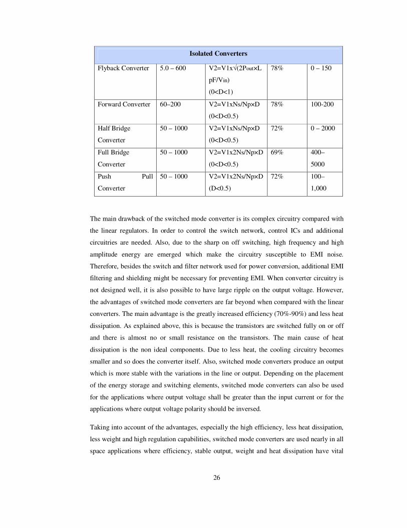
26
Isolated Converters
Flyback Converter 5.0 – 600 V2=V1x√(2Pout×L
pF/Vin)
(0<D<1)
78% 0 – 150
Forward Converter 60–200 V2=V1xNs/Np×D
(0<D<0.5)
78% 100-200
Half Bridge
Converter
50 – 1000 V2=V1xNs/Np×D
(0<D<0.5)
72% 0 – 2000
Full Bridge
Converter
50 – 1000 V2=V1x2Ns/Np×D
(0<D<0.5)
69% 400–
5000
Push Pull
Converter
50 – 1000 V2=V1x2Ns/Np×D
(D<0.5)
72% 100–
1,000
The main drawback of the switched mode converter is its complex circuitry compared with
the linear regulators. In order to control the switch network, control ICs and additional
circuitries are needed. Also, due to the sharp on off switching, high frequency and high
amplitude energy are emerged which make the circuitry susceptible to EMI noise.
Therefore, besides the switch and filter network used for power conversion, additional EMI
filtering and shielding might be necessary for preventing EMI. When converter circuitry is
not designed well, it is also possible to have large ripple on the output voltage. However,
the advantages of switched mode converters are far beyond when compared with the linear
converters. The main advantage is the greatly increased efficiency (70%-90%) and less heat
dissipation. As explained above, this is because the transistors are switched fully on or off
and there is almost no or small resistance on the transistors. The main cause of heat
dissipation is the non ideal components. Due to less heat, the cooling circuitry becomes
smaller and so does the converter itself. Also, switched mode converters produce an output
which is more stable with the variations in the line or output. Depending on the placement
of the energy storage and switching elements, switched mode converters can also be used
for the applications where output voltage shall be greater than the input current or for the
applications where output voltage polarity should be inversed.
Taking into account of the advantages, especially the high efficiency, less heat dissipation,
less weight and high regulation capabilities, switched mode converters are used nearly in all
space applications where efficiency, stable output, weight and heat dissipation have vital

27
importance. In applications such as deployment mechanism drivers, where a well regulated
and controllable output is required the usage of switched mode converters are inevitable.
Power Stage of the driver is supposed to have many external protection circuitries which
disconnect the output load from the main bus voltage in case of a fault. That’s why use of
an isolated converter is not a necessity and in fact due to using transformer isolated
converter has a more complex circuitry to analyze and design. In addition to that, isolated
converters usually contain more components due to need of complex control circuitries.
That’s why isolated converters tend to be heavier and bigger which increases their cost.
Non isolated converters on the other hand have higher efficiency, they have a compact
design and their design and control is relatively simple.
Among the non-isolated converters, buck converter topology is the suitable one for the
power stage of the driver since a voltage step down is required between the bus voltage of
the spacecraft and the thermal knife (MHRM). Also, buck converter is easier to analyze and
implement hence circuit complexity and reduction in reliability is minimized.
2.4 Step-Down (Buck) Converter
As presented in the previous sections, buck converter step downs or chops the input voltage
in order to obtain a lower voltage at the output.
A buck converter mainly consists of two stages; power stage and the feedback control
stage. In the power stage, with the help of two switches, input voltage is turned into pulses
and with the help of a filter the voltage from the switches is filtered and regulated.
In Figure 7, the basic power stage circuitry of Buck Converter is given.
Figure 7 Buck Converter Power Stage

28
The switches of the power stage can be either one controlled (i.e. transistor) and one
uncontrolled (i.e. diode) switch or two controlled switches (in this case the buck converter
is called a synchronous buck converter) [6]. The signals for the switches are obtained from
the control stage. In the control stage, output voltage is measured and then it is compared
with a reference to produce a feedback and then processed to produce the necessary control
signals, namely the PWM signals. With the PWM, the necessary on/off time of the switches
in the power stage are determined in order to hold the output voltage in the desired level.
Detailed description of the control stage and PWM will be given in Section 2.5.
2.4.1 Basic Logic of the Power Stage
In Figure 8, the power stage of a buck converter is given. In this Buck Converter, one
controlled switch, namely a transistor is used. The other switch is a diode.
Figure 8 Buck Converter Basic Logic
The two switches operate such that if one is on the other will be off. Buck Converter has
two states according to these states of the switches. When the high sides switch, Switch 1,
(transistor) is in conduction and low side switch, Switch 2(diode) is reverse biased and
hence it is off, Vin is directly fed to the circuit. So this state is called the ON State. In the
OFF State, SW1 is off and the remaining circuit is completed through the diode, so SW2 is
in conduction.

29
Figure 9 ON State
During the ON State, inductor is fed by the input voltage and inductor stores energy within
its core which results in an increase in inductor current iL and a lower output voltage than
Vin. Inductor voltage is as given in (1).
= + (1)
So, the diode is reversed biased and Switch 2 is Off . In this state, output voltage ripple is
absorbed by the capacitor C.
Figure 10 OFF State
When SW1 is off, SW2 becomes conductive so inductor current continues to flow through
the load. In the OFF State, inductor current decreases linearly and a negative voltage drop
occurs on the inductor (2).
= − (2)

30
Again, by the help of the capacitor, the fluctuations in the output voltage are eliminated. In
Figure 11, Figure 12 and Figure 13, the waveforms during the ON and OFF period for low
side switch voltage Vs, inductor voltage VL and Vout are given.
Figure 11 Waveform for Vs
Figure 12 Waveform for VL
Figure 13 Waveform for Vout
2.4.2 Conduction Modes of the Buck Converter
As mentioned in the above subsection, inductor stores energy and therefore its current
increases during the ON State. During the OFF State, inductor current decreases linearly
until the converter is in the ON State again. During the decrease of the inductor current, the

31
current value may not reach to zero or it may reach to zero and stay there for the rest of the
OFF period.
In the Continuous Conduction Mode, inductor current never falls to zero and it continues to
flow during the whole switching cycle as given in Figure 14.
Figure 14 Waveforms in Continuous Conduction Mode
In the discontinuous conduction mode, the energy need of the load is small enough to be
supplied by the inductor in a duration shorter than the whole off time. So, when this energy
is supplied inductor current reaches to zero and since it cannot be negative, it stays there for
the rest of the toff. During this period when the inductor current stays at zero, SW2 or the
diode becomes reverse biased. So, neither SW1 nor SW2 is in conduction during the rest of
the toff period. When On period starts again, inductor current begins to increase linearly
from zero to its peak value at the end of the On period. Waveforms related to this mode are
given in Figure 15.

32
Figure 15 Waveforms in discontinuous conduction mode
Usually, maximum output power is obtained in the continuous conduction mode so, the
overall performance of the converter is better when compared with the discontinuous
conduction mode [5].In applications where load should be removed or where light loads are
used, DCM are fairly encountered [8]. So, the design of the converter shall be handled
accordingly.
2.4.3 Buck Converter Operation Analysis
The main aim of this section is to derive the output voltage equation in terms of the input
voltage and see the relationship between them. The whole analysis will be done for the
Buck Converter steady state operation in continuous conduction mode. By steady state, it is
assumed that input voltage, output voltage and current are stable or fixed.
Steady state operation implies that the change in inductor current ∆iL is zero which means
that iL has the same value at the begining of the switching cyle and at the end of the
switching cyle. Also, as given in Figure 16, the waveform of inductor voltage vL in one
switching cyle repeats itself in the next cyle.
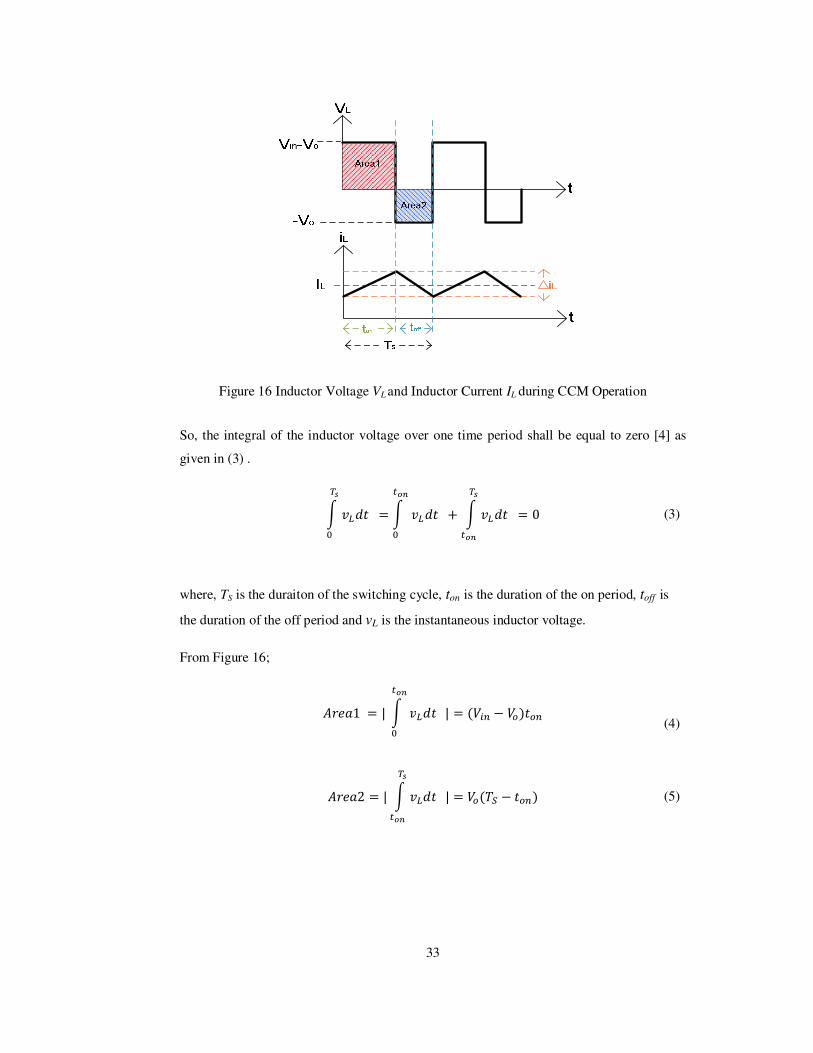
33
Figure 16 Inductor Voltage VL and Inductor Current IL during CCM Operation
So, the integral of the inductor voltage over one time period shall be equal to zero [4] as
given in (3) .
= + = 0
(3)
where, TS is the duraiton of the switching cycle, ton is the duration of the on period, toff is
the duration of the off period and vL is the instantaneous inductor voltage.
From Figure 16;
1 = | | = ( − )
(4)
2 = |
| = ($% − ) (5)

34
where, Vo is the DC value of the output voltage and Vin is the input voltage.
Since Area1 must be equal to Area2 in order to keep the inductor current ripple at zero;
( − ) = ($% − ) (6)
Arranging this equation;
& = $% = ' (7)
In (7), the parameter “D” refers to the duty ratio. It is the ratio that determines the on time,
ton, in one switching cycle, TS. Duty ratio is a number that is between 0 and 1. As can be
seen from (7), output voltage of the converter is dependent only on the input voltage and
the duty ratio. So, output voltage can be adjusted by simply setting an appropriate value for
the duty ratio, D. Since D is between 0 and 1, output voltage is always smaller than the
input voltage, which creates the specific feature of the step-down (buck) converter.
2.4.4 Selection of the Components in the Power Stage
2.4.4.1 Inductor
Inductor in a buck converter is used both for storing the necessary energy that will be
transmitted to the load and for limiting the current ripple in addition to the in rush current
which arises due to the switching of the transistor.The main factors for determining the
inductor size are the current ripple that must be achieved and the peak current that the
inductor has to tolerate. Also, inductor value shall be chosen according to the mode
(continuous or discontinuous) that the converter will operate.
There are many off the shelf products for inductors, however some analysis shall be
conducted to see if the converter requirements are in line with the selected product. A
realistic and detailed analysis is given in [11]. According to this analysis, the current
waveform of the inductor can be divided into its components and these componenets can be
used to calculate the necessary inductor parameters.

35
Figure 17 Inductor Current Waveform
As can be seen from Figure 17, instantaneous inductor current iL has AC and DC
components on it. IDC is the average or DC value of the inductor current. IDC is also equal to
the load current Iout. Ipeak is the peak value of the inductor current and given as in (8).
()*+, = (- + ∆//2 (8)
Ithrough is the constant residual current on the inductor. This current depends on the load and
changes according to the converter being in the continuous or discontinuous mode and is
given as in (9).
(1231 = (- − ∆//2 (9)
And from (8) and (9), the peak to peak current ripple ∆/ is
∆/ =()*+, −(1231 (10)
Defining the ratio of AC to DC components of iL as the current ripple ratio “r” at maximum
load current [11];
= ∆/( (11)
“r” is defined for the continuous conduction mode and for the specific converter
application. The upper limit of “r” before transition to discontinuous mode of operation is
given as “2” [11]. This is because, if the load is reduced, ripple current stays the same but
the DC current is reduced also and at the boundary of the continuous to discontinuous mode
transition, IDC is ∆//2 .

36
From “r” and the basic equation for the inductor voltage, required inductance L can be
calculated as given in [11].
= 4 /
(12)
During the ON duration,
= −56 − (13)
/ = ∆/ (14)
= 78 = ' × $: = '/; (15)
where D is the duty cycle, Ts is the switching cycle and f is the switching frequency.
So by implementing (13),(14) and (15) into (12);
−56 − = 4 ∆/'/; (16)
Combining equations (11) and (16), r can be expressed as ;
= (−56 − ) × '4 × ; × ( (17)
Knowing that;
' = 7</8 (18) And including the voltage drops on the switch Vsw and diode Vd , (18) becomes;
& + = += − 56 = ' (19)
So,“r” can be written as
= (−56 − ) × (& + =)( += − 56) × 4 × ; ×( (20)

37
From this equation L can be found as;
4 = (−56 − ) × (& + =)( += − 56) × × ; ×( (21)
As seen from (21), L can be determined by the ripple ratio “r”, switching frequency “f”,
maximum load current Iout and the necessary voltage values for the buck converter that
will be designed.
When an inductor is saturated, the effective inductance is dropped by a specific amount and
it behaves as a short circuit under DC current. This is because inductor core core can not
store any more magnetic energy. This causes an increase in the inductor, transistor and
diode temperatures in addition to a decrease in the converter efficiency [12]. So, the
inductor shall be chosen such that it can withstand the peak current without becoming
saturated. This is determined by the energy handling capability “e” of the inductor [11].
= 12 × 4 × ()*+, (22)
From (8) and (22), it seems that reducing the inductance may result in a higher ripple in
current (∆i?) and in turn the energy handling capacity will increase. However, as stated in
[11], the situation is exactly the opposite. Energy handling capacity can be rearranged in
terms of “r” as given in (23).
= ( × @8 × B × (2 + 1)C DE (23)
Where Et is the multiplication of the voltage applied to the inductor winding and the
duration of this voltage application in µsecs. So;
@ = × ∆ = 4 × ∆(D:F (24)
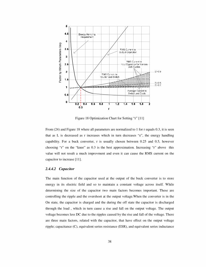
38
Figure 18 Optimization Chart for Setting “r” [11]
From (24) and Figure 18 where all parameters are normalized to 1 for r equals 0.3, it is seen
that as L is decreased as r increases which in turn decreases “e”, the energy handling
capability. For a buck converter, r is usually chosen between 0.25 and 0.5, however
choosing “r” on the “knee” as 0.3 is the best approximation. Increasing “r” above this
value will not result a much improvment and even it can cause the RMS current on the
capacitor to increase [11].
2.4.4.2 Capacitor
The main function of the capacitor used at the output of the buck converter is to store
energy in its electric field and so to maintain a constant voltage across itself. While
determining the size of the capacitor two main factors becomes important. These are
controlling the ripple and the overshoot at the output voltage.When the converter is in the
On state, the capacitor is charged and the during the off state the capacitor is discharged
through the load , which in turn cause a rise and fall on the output voltage. The output
voltage becomes less DC due to the ripples caused by the rise and fall of the voltage. There
are three main factors, related with the capacitor, that have effect on the output voltage
ripple; capacitance (C), equivalent series resistance (ESR), and equivalent series inductance

39
(ESL). Capacitance and ESR value requiered for an acceptable ripple will be calculated
below.
In the continuous conduction mode of operation and assuming that all the ripple component
of the inductor current iL flows through the capacitor, the shaded area given in Figure 19
represents the additional charge on the capacitor [4]. So, the peak to peak output voltage
ripple,∆ , can be written in terms of the additional charge on the capacitor,∆G, and the
capacitance C as given in (25) Where ∆( is the inductor current ripple and $% is the
switching period.
∆ =∆GH = 1H × 12 × ∆(2 × $%2 (25)
Figure 19 Buck Converter Output Voltage Ripple
As it is seen from (25) and (26), a larger capacitor will reduce the ripple voltage. If (26) is
written in terms of the inductance value L, then;
∆( = 4 × (1 − ') × $% (26)

40
Substituting ∆( from (26) into (25);
∆ = $%8H × 4 × (1 − ') × $% (27)
∆ = 18 × $%(1 − ')4H = I2 × (1 − ') × J;K;5L (28)
where ;5 is the switching frequency as given in (29);
;5 = 1$5 (29)
and ;K is the corner frequency of the output LC filter as given in (30);
;K = 12I√4H (30)
If the corner frequencyof the output LC filter is chosen such that fc << fs, then the output
voltage ripple can also be decreased.
In addition to the capacitor value, ESR is one of the factors affecting the voltage ripple. In
fact, ESR dominates the effect of the capacitance on the voltage ripple. If the capacitor
value is selected such that its effect on the ripple can be ignored, than the ESR value can be
arranged according to the desired ripple level as in (31) since Vripple = I ripple x ESR;
@NO ≤ ∆∆( (31)
Usually, the capacitor value which meets the specified ESR value will be greater than
needed, so selected ESR shall be a reasonable value. Besides, if ESR is too high, the output
voltage ripple will increase dramatically and the power loss on the capacitor due to the ESR
and ripple current will be higher.
Q=55 = (2))R* × @NO (32)

41
Power dissipation causes heat which shortens the expected life of the capacitor. Also,
capacitors have ripple current rating which shall not be exceeded. The RMS value of the
ripple current flowing on the capacitor can be given as in (33) and this rating shall be taken
into account while choosing the capacitor.
(-ST% = ∆( × √36 = ∆( × (0.289) (33)
ESL is another factor that affects the ripple voltage. However, it is not usually specified in
the manufacturers’ datasheets. Generally, ESL becomes effective for the switching
frequencies above 1MHz. For such applications, ESL value shall be learned from the
manufacturer. Usually, for all applications, choosing a low ESL capacitor, limiting the lead
length of the capacitor and PCB traces and using smaller components in parallel overcomes
this problem.
Another issue on which the output capacitor has effect is the overvoltage problem.When the
full load is suddenly removed, output voltage overshoots its regulated value due to the
launched inductor energy at the output. This energy causes the output voltage to be above
the specified maximum level. So, the output capacitance shall be high enough to prevent
the voltage overshoot. Output voltage overshoot can be calculated as given in (34) , [12].
∆Y*251 = Z[\] + 4 ^(_+` +∆(2 a
H_+` bcd − (34)
where Cfgh is the maximum output capacitance and ∆Vjklmnojjp is the maximum output
voltage overshoot. So the capacitor value to overcome this problem is;
H_+` = 4 ^(_+` +∆(2 a(∆Y*251 + )− (35)
For selecting the output capacitor for the specific application, the requirements for ripple
and overvoltage on the output shall be taken into account.

42
2.4.4.3 Power Switch
The aim of the power switch in a converter is to connect the input supply to the output
voltage. Switch is used to conduct current to the inductor when it is on and to block the
input supply completely when it is off. So, the switch shall be able to turn on and off
quickly in order to reduce the power dissipations during the switching transitions. In
addition, the switch shall be able to withstand the voltage spikes produced by the inductor.
Power switch for the converter is usually selected by the converter parameters such as cost,
switching frequency, load current and the off-state voltage handling needs for the switch.
There are three main choices that can be used as a power switch for the converters [13].
Bipolar Junction Transistor (BJT), Power MOSFET and Integrated Gate Bipolar Transistor
(IGBT).
BJTs are current controlled devices which require a considerable amount of base current as
a portion of the collector current. This makes the control of BJTs harder than the other
switches. Also, due to their switching characteristics BJTs are used for applications with
switching frequencies less than 80-100 KHz [13]. However, BJTs are advantageous due to
their cost and still preferred for high power applications with low switching frequencies.
MOSFETs are voltage controlled devices. It is easier to turn on and off the MOSFETs since
their gate current need is small. So, MOSFETs are easier to control when compared with
the BJTs. The most important characteristic of MOSFETs is that they can operate at higher
switching frequencies. They can be used for applications where operating frequency is
above 200 KHz. But, since they have a large on resistance which increases dramatically
with the raise of MOSFETs’ breakdown voltage, they are usually preferred for applications
with voltage rating smaller than 500V.
IGBTs are typically a transition between the BJTs and the MOSFETs. IGBTs are used for
high voltage and high power applications. They can be used for the operating ranges above
1000V due to their high breakdown voltages. Like MOSFETs, IGBTs also have an easy
control mechanism due to its low power drive characteristics. However, IGBTs can only be
used for operating frequencies below 100 KHz [14].
Considering the ease of control, simplicity of the drive circuitry and the ability to operate at
high switching frequencies MOSFETs are preferred for various converter applications. So

43
the details of MOSFET selection criteria according to the specific application that it will be
used as a switch will be given hereafter.
In order to decide on the MOSFET to be used, voltage and current characteristics as well as
the power dissipation on the switch shall be considered with respect to the converter
requirements.
One of the basic parameters for a MOSFET is the on time resistance of the switch, RDSon.
RDSon is the cause of the on time power dissipation on the switch. Also, RDSon changes with
temperature and its value shall be evaluated accordingly for power dissipation calculations.
If the value of RDSon for the required temperature range can not be found in the datasheets,
(37) can be used for an approximation [15].
O%(q&) = O%(%rs-) ∙ u1 + 0.005 ∙ ($w(q&) −$w(%rs-))x (36)
where RDSon(SPEC) is the specified RDSon value corresponding to the junction temperature
Tj(SPEC), and RDSon(HOT) is the calculated RDSon value at the operating temperature Tj(HOT).The
on time power dissipation on the MOSFET can be calculated as in (37) where QS% is the
power dissipation due to RDSon and RDSon(HOT)is calculated as given in (37).
QS% = × (_+` × O%(&y)q& (37)
If the input voltage varies, then power dissipation shall be calculated both for _ and _+`. At_, power dissipation will be higher due to the factor Vout/Vin of (37).
Another factor contributing the power dissipation is the switching losses. A rough
approximation for switching losses is given in [15] as;
Q56K13 = zHS%% × × ;56 × ((|s (38)
where HS%% is usually specified in the MOSFET’s datasheet and it is the MOSFET's
reverse-transfer capacitance, (|s is the MOSFET gate-driver's sink/source current at

44
MOSFET's turn-on threshold and ;56 is the switching frequency. Again, if Vin varies, then
switching losses should be calculated for _+`due to the term in (38).
Usually, on time power dissipation and the switching power dissipation can be chosen as
equal for minimizing the power losses. A larger MOSFET will have a smaller RDSon and a
smaller resistive power loss but switching losses will increase in turn. This is because as the
MOSFET gets larger the gate capacitance increases which affects the turn on and turn off
times of the MOSFET. A smaller MOSFET on the other hand, will have smaller switching
losses due to having a smaller gate capacitance and so being faster, but this will increase the
resistive power losses as a consequence. So, as stated in [12] and [15], a good balance
between the resistive and switching losses (usually equality or resistive losses being the
60% of the total power losses) should be considered.
In addition to power losses, voltage and current ratings shall also be considered during the
selection of the power switch. For this, the maximum drain current, ID(Max) and the
maximum drain-to-source breakdown voltage, V(BR)DSS, shall be evaluated. As a general rule
and as stated in [7], the V(BR)DSS rating of the selected MOSFET should be greater than the
maximum input voltage with the necessary margins added for transients and spikes. Also,
the ID(Max) rating of the MOSFET should have a value of at least two times the maximum
output current of the power stage.
Another parameter for selecting MOSFET is the junction temperature. This temperature is a
specified maximum value for the MOSFET to operate reliably. So, junction temperature
should be calculated in order to guarantee that it is not exceeded.
$~ = $ + Q × O~ (39)
Where, TA is the ambient or heatsink temperature, PD is the total power dissipation on the
MOSFET and O~ is the thermal resistance from the MOSFET chip to the ambient air or
heatsink [7].
2.4.4.4 Diode
In converters where one switch is active and the other one is passive, usually diode is used
as the passive switch. The aim of using the diode is to create a current path for the inductor
when the power switch (transistor) is off. When the power switch is on again, diode

45
becomes reverse biased and the current from input source flows through the inductor. So,
the diode enables a path for the inductor to deliver its stored energy to the load.
Key elements for choosing a suitable diode are the power dissipation (related with the
forward voltage drop of the diode), fast switching, current rating and breakdown voltage.
Adding some margin for the spikes and the transients, the breakdown voltage (maximum
reverse voltage, VR or the reverse repetitive maximum voltage, VRRM) of the diode should
be greater than the maximum input voltage. Also, the maximum average forward current
rating of the diode (IFAV) shall be at least two times the maximum current of the power
stage.
As in the power switch case, power dissipation is maybe the main factor that affects the
diode selection. Since diode is conducting only during the Off period and the power losses
due to switching losses are very small, power dissipation on the diode can be calculated as
in (40), [7].
Q==* = (1 − ') × × ( (40)
Where Q==* the power dissipation on the diode, D is is the duty cycle, is the forward
voltage of the diode and ( is the maximum output current during the period while diode
is conducting. If the input voltage is varying then, D should be calculated for _+`. Since D is as given in (7) the parameter (1-D) in (40) will take the maximum value at Vfgh. So, power dissipation for the worst case can be calculated. In order to guarantee a
reliable operation and a long life time for the diode, the junction temperature limits should
not be exceeded also. (39) can be used to see if the limits are exceeded.
During the selection of a diode, it is important to keep the power dissipation low in order to
increase the converter efficiency. Power dissipation of the diode can be lowered by
selecting a diode with low forward voltage drop. Silicon diodes have a forward voltage
drop of 0.7V, where Schottky diodes have a forward voltage drop of 0.3V. Usually
Schottky diodes are used in converter applications where the remaining factors mentioned
above are met. In some applications such as synchronous buck converters, the diode is
replaced by a transistor in order to further reduce the power dissipation. With low RDSon the
power dissipation on the transistor will be much less than that on the diode, especially for
the low duty cycles. However, using a second transistor causes complexity in the control
circuitry. Diode turns itself on and off according to the power switch transistor, but if a

46
transistor is used instead of the diode, then this transistor needs to be turn and off
synchronously with the power switch transistor by a complementary-output switch driver in
order to have a continuous current flow. So, choosing between a diode and the transistor
depends on the application needs, cost and the complexity that can be handled.
2.5 Control Methods in Step-Down (Buck) Converter
2.5.1 Control Stage of the Buck Converter
As mentioned in Section 2.4, buck converter uses one or two controlled switches (one
transistor and diode for the non synchronous buck converter and two transistors for the
synchronous buck converter) in order to get the desired output voltage by turning on and off
these switches by the help of the control stage. PWM (Pulse Width Modulation) is used for
controlling the switches. In PWM, the switching frequency and in turn, the switching
period (Ts = ton + toff) is fixed. So, the duty cycle is arranged according to the feedback
obtained from the output so that switches stay “ON” to provide the desired output voltage.
Figure 20 Control Stage of the Buck Converter
In order to obtain the PWM signals that control the switch, the difference between the
actual output voltage and the desired output voltage is amplified and compared with a
repetitive waveform as shown in Figure 20 and Figure 21. Repetitive waveform is usually a
sawtooth or a triangular waveform and its frequency determines the switching frequency of
the converter. The value of the amplified error signal varies slowly within time [4]. When

47
s222_) >% , switch is turned on to decrease the error amplifier output by increasing
the output voltage. When s222_) < % , switch is turned off.
Figure 21 PWM Pulses
One of the main challenges while designing a DC/DC converter is the control stage (or the
feedback control system) which will met the steady state and the transient response
requirements of the converter. The basic demand for the feedback control system is that it
will enable the DC/DC converter to reject any disturbances due to the various sources of
noise, input and output line variations so that the converter will have a well regulated
output. The optimum feedback loop that is used for producing the PWM should respond
neither too fast nor too slow [16]. If the feedback loop is too fast and the duty cycle is
changed suddenly in large amounts, output voltage may be over corrected before the
control loop realizes the situation. So, output voltage will be higher or lower than the
reference voltage (or the desired voltage). In this case, control loop will react to correct this
situation but again, since the change in the duty cycle is fast and large, output voltage will
be over corrected once more. The process will go on like this and there will be “ringing” in
the output voltage. “Ringing” can die after some switching cycles or it may continue
forever in the worst-case. In the latter case, converter will become fully unstable with
oscillations. If the feedback loop is too slow duty cycle will be changed slowly and
gradually. When the desired output voltage level is reached, controller stage will react to
keep it but due to being slow, there will be “overshoot” or “undershoot” at the output. So,
control loop analysis should be carried out to see the effect of any disturbance and obtain an
overall system which is stable with the control loop added, which means perturbations

48
introduced to the overall system eventually die out and hence output voltage regulation is
kept. A stable system is considered to have a good steady state and dynamic response.
Steady state response is related to the power stage and usually handled by determining the
parameters of the power stage properly. Dynamic response on the other hand depends on
the control stage design. In order to obtain a stable system in the sense of steady state and
dynamic responses, open-loop and closed-loop transfer functions of the overall system are
studied. Open-loop gain is the total gain around the feedback loop and shows how much
output error results due to any disturbance at any point in the loop compared to the situation
when the loop is open. Closed loop gain, on the other hand, gives a definition on the output
to control input relationship.
Characteristics of the open loop transfer function,$&(:), for a stable system can be given
as below [4];
• Crossover frequency wc of $&(:) should be as high as possible since this is the
frequency at which the gain of $&(:) falls to 1. However, wc should be an order of
magnitude below the switching frequency so that overall system can respond the
transients quickly.
• Phase margin of the system is supposed to be in a range of 45o-60o for a good
transient response to load and line variations. Phase margin, which is a positive
quantity, can be determined as;
Qℎ:/8 = ∅& + 180H (41)
• In order to minimize the steady state error in the output and have a tight voltage
regulation, gain of T?(s) should be high at low frequencies.
• To prevent a large overshoot at turn on and during transients, mid-frequency gain
should be greater than zero.
It is easier to perform the above mentioned analyses on the linear systems. However, the
pulse width modulator and the power stage of the converter is not perfectly linear.
Assuming that the disturbances are small enough, a linear model of the power stage
including the output filter can be linearized around a steady state DC operating point [4].
This technique is called “State-Space Averaging” and introduced by R. D. Middlebrook at
Power Electronics Group - California Institute of Technology, USA. Using this technique,
each block given in [4]can be linearized and the feedback loop analysis can be performed
accordingly.

49
2.5.2 Control Methods
2.5.2.1 Voltage Mode Control
Voltage mode control is the oldest technique used for the design of the first regulators.
Since then it is widely used in the industry due to its simplicity. In voltage mode control,
the output voltage of the converter is measured and it is compared with a reference voltage
in an error amplifier where the error is compensated according to the stability needs of the
system. Then the output of the error amplifier is fed to a comparator with a ramp waveform
where the necessary PWM signals are produced. Basic blocks for the voltage mode control
is given in Figure 22
Figure 22 Voltage Mode Control
Since voltage mode control is based on a single feedback loop, it is usually easy to design
and implement. Also, using a large amplitude ramp waveform enables a good noise margin
for stable operation conditions. However, due to the use of the output voltage as feedback,
any change in input voltage cannot be immediately sensed. First, this change should be
transferred to the output so that the control loop can sense it. The same situation is also
valid for any load change. That’s why voltage mode control has a slow response to any line
or load change. Also, since the input voltage is the main factor for the loop gain, any
change in input voltage varies the loop gain, which makes the compensation to become
complicated. Input voltage feed forward circuitries can be used to overcome this problem.

50
2.5.2.2 Current Mode Control
In current mode control, an additional current loop is implemented into the voltage control
loop. This inner current loop senses the inductor current and turns the inductor into a
voltage controlled current source. So, for dc and low frequency, the inductor is removed
from the outer voltage control loop [21] which in turn results in a simpler compensation
circuitry as well as increased gain bandwidth with respect to a comparable voltage mode
controller.
Figure 23 Current Mode Control
Since inductor current is directly used for feedback purposes and its slope is changing with
Vin-Vo, current mode control has a fast response for line and load variations and gain
variation according to the input voltage is not a case in the current mode control. Despite of
its many advantages, current mode control also have its own problems. First of all, since
two feedback loops are used, analysis and implementation of these circuitries are difficult.
Using the inductor current for feedback causes resonances produced in the power stage may
insert noise into the control loop. Noise immunity is also worse due to using a shallower
ramp signal compared to a voltage mode controller. But, the most important problem of the
current mode control is the open loop instability which is caused by the difference between
the sampled inductor current value and the average inductor current value for duty cycles
above 50%. Above this level, sub harmonic oscillations occur since the inductor current
ripple does not return to its initial value by the start of the next cycle [21] and the control
loop becomes open loop unstable. In order to overcome this, a compensation ramp is added
to the circuitry.

51
Figure 24 Slope Compensation in Current Mode Control
The corrective ramp as shown in Figure 24, can be added to the control loop by either
adding it to the sensed inductor current or subtract is from the control voltage. The slope of
the compensation ramp is equal to or greater than one half of the inductor current’s down-
slope. By this slope, the level at which the loop becomes unstable and disturbances are
magnified can be lowered. With slope compensation, line changes can be rejected in a great
amount depending on the slope of the line added. However, the response to sudden load
changes may degrade.
Figure 25 For D < 50%, disturbances die out with each cycle

52
Figure 26 For D > 50%, disturbances grow with each cycle and sub-harmonic oscillations
are observed
Figure 27 With Slope Compensation Disturbances Die Out with each cycle and for any D
2.5.2.3 Types of Current Mode Control
There are several types of current mode control and the mostly used ones are the Peak
Current Mode Control (PCMC), the Valley Current Mode Control (VCMC), the Emulated
Current Mode Control (ECMC), the Hysteresis Current Mode Control (HCMC) and the
Average Current Mode Control (ACMC). PCMC, VCMC, ECMC and ACMC are used for
fixed frequency operations whereas HCMC is used for operations with varying frequency.
In Peak Current Mode Control (PCMC), the peak inductor current is sensed when the
switch is on and the switch is turned off if its value is greater than the output of the error
amplifier. Such a control on the “turn off” of the switch is named as "trailing edge
modulation".
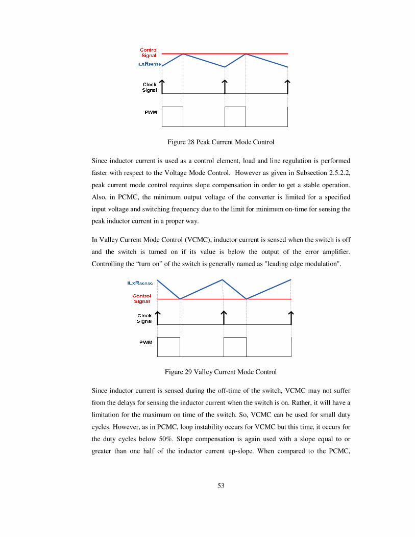
53
Figure 28 Peak Current Mode Control
Since inductor current is used as a control element, load and line regulation is performed
faster with respect to the Voltage Mode Control. However as given in Subsection 2.5.2.2,
peak current mode control requires slope compensation in order to get a stable operation.
Also, in PCMC, the minimum output voltage of the converter is limited for a specified
input voltage and switching frequency due to the limit for minimum on-time for sensing the
peak inductor current in a proper way.
In Valley Current Mode Control (VCMC), inductor current is sensed when the switch is off
and the switch is turned on if its value is below the output of the error amplifier.
Controlling the “turn on” of the switch is generally named as "leading edge modulation".
Figure 29 Valley Current Mode Control
Since inductor current is sensed during the off-time of the switch, VCMC may not suffer
from the delays for sensing the inductor current when the switch is on. Rather, it will have a
limitation for the maximum on time of the switch. So, VCMC can be used for small duty
cycles. However, as in PCMC, loop instability occurs for VCMC but this time, it occurs for
the duty cycles below 50%. Slope compensation is again used with a slope equal to or
greater than one half of the inductor current up-slope. When compared to the PCMC,

54
VCMC has a slower response to the line changes, but a better response for the load changes
due to the need for delay to sense the inductor current in PCMC.
Emulated Current Mode Control (ECMC) can be thought as a combination of the PCMC
and the VCMC. In PCMC, the inductor current ramp is sensed and turned into voltage for
comparison with the output of the error amplifier. However as mentioned in PCMC, such a
measurement method has a very limited time range for gathering the actual current ramp
value during the on time of the switch. So, especially for high input and low output
applications where very small on-times are needed ECMC can be used. In ECMC, the ramp
is emulated by use of a capacitor for the on-time. When this ramp is greater than the output
of the error amplifier, the switch turns off. During the off time, the inductor current is
sensed and compared with the error amplifier output. So, when the switch is turned on
again, the valley current of the inductor becomes the beginning value of the emulated
current ramp. In other words, the valley current of the inductor is sampled on the down
slope of the inductor current and used as a starting point for emulating the inductor current
up-slope. ECMC has the advantage of operating at low duty cycles as VCMC since no on-
time current sense is performed. This also removes the need for a high side current sense
amplifier, which simplifies the design. Besides, ECMC has the advantage of fast response
to load and line changes. However, as mentioned in the previous CMC methods, ECMC
also suffers from sub-harmonic oscillation and slope compensation must be added with a
slope greater than half of the sum of the inductor up-slope and down-slope to overcome the
oscillation.
Due to the limitations of constant-frequency operations in CMC, alternative methods such
as Hysteresis Current Mode Control (HCMC) are developed. In HCMC, inductor current is
sensed by a differential current sense amplifier and its output is used to drive two
comparators for the peak and valley values of the inductor current. With a reference that is
used in the input of these comparators’ input, a hysteresis band is obtained. When peak
current of the inductor exceeds the upper limit of the band, the switch is turned off and
when the valley current reaches the lower limit of the band, the switch is turned on.When
input voltage is changed, the on time of the switch is also changed according to the desired
output voltage. However, hysteresis band and the slope of the discharge current are constant
and therefore switching frequency changes in return. One of the results of this situation is
that inductor current peak and average current difference does not change as in the case of
the constant frequency control [22]. Advantages of HCMC are ease of loop stability, no sub

55
harmonic oscillations, no limitations on the minimum and maximum on-times, superior
response to line and load variations. However, the applications where HCMC can be used
are limited and HCMC cannot be used for any applications that need to synchronize the
supply's switching frequency with some external clock [22].
Average Current Mode Control is another methodology for controlling the converter. In
ACMC, inductor current’s average value is used as a control parameter and it is
compensated dynamically by a high gain current compensator circuitry within the current
loop. As in the other current mode control methods, desired current level is set by the outer
voltage loop. Desired current level and the actual inductor current sensed and amplified
through a current sense amplifier are fed into the current compensator. The difference
between them is compared to a large amplitude sawtooth waveform at the PWM to generate
the necessary duty cycles. Average current mode control does not require slope
compensation as in the other CMC techniques since the average value of the inductor
current and the sampled inductor current are the same, so and it has excellent noise
immunity during switching. In average current mode control, since the sensed current is
compensated by a high gain current compensator, the current ramp is higher than that is in
the other current mode control topologies. Hence, current ramp is not easily affected by the
noise spikes such as the one that is generated during the switching. Hence, average current
mode control has better noise immunity than the other current control methods. Also,
ACMC has an excellent accuracy while tracking the current that is desired since the sensed
and the sampled inductor current are the same. So, ACMC enables the converter to behave
as an ideal current source and this control method becomes preferable especially for
applications where a constant current source is required.
Due to the need of a constant current source during the specified operation periods of the
Thermal Knife Actuator and due to its ability to track and control the desired current level
excellently, ACMC becomes preferable as the control methodology for the buck converter.
Besides, ACMC has low switching noise and better noise immunity which are critical
features due to the strict specifications of the space applications on noise characteristics.
Also, it is easier to put a current limit on the converter which is one of the requirements of
the power stage that is designed. Because of its advantages when compared with other
methodologies and because of the requirements of the Thermal Knife Actuator, ACMC is
chosen as the control topology.

56
2.5.3 Average Current Mode Control
In Figure 30, a general circuit for the ACMC is given. In ACMC, inductor current is sensed
by the resistor Rs and it is converted into voltage by the current sense amplifier. Output of
the current sense amplifier can be written as vl(t)=Ri iL(t). Ri is the total current sense gain
and it is equal to the product of the current sense resistor Rs and the gain of the current
sense amplifier, ACL.
Figure 30 Average Current Mode Control
Output of the current sense amplifier, vl(t), is compared with the output of the voltage loop
controller, vva(t), which represents the required average inductor current. The difference of
the vl(t) and vva(t) are processed in the current compensator and compared with the PWM
oscillator signal vm at PWM comparator. The output of PWM comparator is fed to the
switches.
A buck converter using ACMC can be divided into functional blocks which are namely the
power stage, current compensator, voltage loop controller and the modulator. Each block
can be modeled separately and studied in terms of small signal analysis in order to design
the control loop and to obtain a complete model of the buck converter with ACMC.

57
In order to study, design and examine the average current mode controlled switch mode
converters state space averaging technique can be used. With this technique the complexity
of the small signal analysis where large signal analysis is omitted and complexity is
increased due to sampling effect of the current mode controlled converters. In order to
study the DC operating point of the buck converter with ACMC, determined the stability,
loop gain and transient response of the converter, state space averaged model of the
converter is derived.
2.5.3.1 State Space Averaged Model of the Buck Converter with ACMC
A state spaced averaged model for the buck converter with ACMC is given in Figure 31.
Here, each stage of the converter is represented by constructing blocks.
Figure 31 Block Diagram of State Space Averaged Converter Model [62]
In [62], the proposed state space averaged model is performed by modeling the power stage
of the converter and the modulator separately and then obtained results are combined with
the current compensator and voltage controller.
In order to model the power state with the state space averaging technique in continuous
conduction mode, linear circuit is described for each circuit state (on state and the off state)
in terms of state variable x.
= + </8ℎOnState→. $5 (42)
= + </8ℎOffState→(1-). $5 (43)

58
In the above equations, consists of the inductor current and the capacitor voltage. and are state matrices and and are vectors. Averaging and time weighing the
following circuit states together, an averaged model of the power stage is written as in (44)
[4].
= +(1 − ) + + (1 − ) (44)
In [62], the averaged model of the power stage is given using a matrix of transfer functions
and Laplace transform taking into account that small signal behaviour is of interest.
-(:)((:) = B Y(:) =Y(:) K(:) =K(:)C 3(:)'¡(:) (45)
Here, =K(:) is the duty ratio to inductor current transfer function and =Y(:) is duty ratio
to capacitor voltage transfer function.
From the state space averaged model of the buck converter =K(:) and =Y(:) can be
written as;
F(:) = 1 + (O + K)H:O + (4 + OHK): + (O4H + K4H): (46)
(:) = 1 + KH:O + (4 + OHK): + (O4H + K4H):
(47)
d iL viLvcr vcl
Figure 32 Current Loop Block Diagram

59
Giving the block diagram of the current loop as in Figure 32 [68], “Current loop gain” Tc
can be derived as
$F(:) = O¢_ F(:) F(:) (48)
where F is the current compensator transfer function as given in (53). ¢_ is the transfer
function of the PWM modulator and ¢£ = 1/£ where £ is the peak to peak voltage of
the oscillator ramp. O is the total current sense gain multiplied by the sense resistor as
given in Subsection 2.5.3.
The product O¢_ F(:) can be named as the power stage for the current loop and shown
as;
¤F¥(:) = O¢_ F(:) (49)
From (48) and (53), Tc can be written as;
$F(:) =O¢_ 1 + (O + K)H: F(:)O + (4 + OHK): + (O4H + K4H):
Main design criteria for the construction of Tc are to obtain enough gain bandwidth and
phase margin. Crossover frequency for Tc is recommended to be as high as possible but at
least one decade below the switching frequency of the converter to let enough time for the
control loop to response sudden changes [4]. Usually, a crossover frequency between one
sixth and one tenth of the switching frequency is a good compromise. At the crossover
frequency of the current loop, the phase margin the recommended value is between 45o and
60o to obtain a well damped and stable system. Considering other criteria for the stability,
general considerations mentioned in Subsection 2.5.3.2 and Subsection 2.5.3.3 are to be
taken into account. In order to obtain the desired Tc, current compensator design should be
studied such that location of the poles and zero and the value of the current compensator
gain are adjusted with respect to the rules defined in Section 2.5.3.2 and as a result, the
desired gain bandwidth and the phase margin for Tc are obtained.
In the same manner with Tc, control to inductor current transfer function Tic with current
loop closed can be written. Expressing the output signal KR(:) of the current compensator
with respect to the inputs of the compensator (50) can be obtained.

60
KR(:) = K(:) + ¦K(:)uK(:) − O((:)x (50)
Where
¦F = 1 + F (51)
According to this equation control to inductor current transfer function Tic can be written
as [62];
$K = ((:)K(:) = ¢_¦F(:) + 1 F(:)$F(:) + 1 (52)
2.5.3.2 Design of the Current Compensator
Figure 33 Current Compensator
A general approach for the construction of the current compensation circuitry is to use a PI
controller with an additional high frequency pole. This scheme is given in Figure 33 and it
is usually named as “Type 2 Compensation”. Transfer function of this scheme can be
written as;
F(:) = ¢F 1 + : §¨K+©:(1 + : §)K+© ) (53)
where;
¢F = 1OR(Hª) + Hª¨) (54)

61
§¨K+ = 1OªHª¨ (55)
§)K+ = Hª¨ + Hª)OªHª¨Hª) (56)
As can be seen from the transfer function, Gca(s), the compensation network consists of a
pole at the origin which pushes the DC gain and the low-frequency gain of the current loop
to infinity. However, this pole causes a 90 degrees of phase drop which is compensated by
the zero, §¨K+ . This zero is also needed to extend the crossover frequency of the current
loop. By §¨K+ , the phase margin is brought to the desired level as mentioned in Subsection
2.5.3.1 and the low frequency gain is boosted, so current loop can answer the demand of the
outer voltage loop in a fast and accurate manner. A general rule for setting the value of §¨K+ is to place it between the one third and half of the power stage resonant frequency w0
in order to extend the current loop crossover frequency [62, 61]. Another approach is to
place §¨K+ at least one decade before half the switching frequency [63]. According to the
stability needs, a suitable value for §¨K+ can be chosen according to these approaches.
The high frequency pole, §)K+, is used to eliminate the switching noise and the ripple. With
the zero, §¨K+ and the pole, §)K+, phase margin at the cross over frequency can be settled at
a suitable level. While settling the value for §)K+, it should be placed as close as possible
to the switching frequency in order to obtain sufficient filtering for the switching ripple. A
lower limit for placing this pole can be after half the switching frequency [63].
The DC gain, Kca, of the compensation network shall also be adjusted carefully. This is
because, if the slopes of the waveforms at the two inputs of the PWM comparator are not
properly adjusted, sub harmonic oscillations will occur. This situation is solved by slope-
compensation in other current mode control methodologies as mentioned in Subsection
2.5.2.2. In ACMC, oscillator (sawtooth waveform) ramp has enough slope compensation.
However, the down slope of the output of the current compensator, which is the other input
of the PWM comparator, is amplified and inverted during the Off-Time of the switch as
shown in Figure 34.

62
Figure 34 PWM Pulses and Control Voltage Waveforms
So, the upslope of the waveform at the current compensator output shall not exceed the
oscillator ramp slope in order to avoid subharmonic oscillations [64]. In [64], it is advised
to set the value of the upslope of the current compensator during the Off-Time equal to the
slope of the oscillator ramp, Vm. However, in practical designs, the ripple amplitude vd at
the output of the current compensator may be high and it will be clipped when it reaches the
lower limit of the current amplifier [62]. This will also cause switching instability
especially at low duty ratios, since the modified slope of vd can be higher than the oscillator
ramp when the clipping is removed. So, as the method in [62] suggests, a limit for the DC
can be set at switching frequency by limiting the ripple amplitude of vd.
Since the DC gain can be approximated as equal to Rf/Rl at switching frequency, this limit
can be written as;
OªOR ≤ £/8 2_4;5(3,_+` − )O5 , _4;5O5 (57)
This limit will ensure that switching ripple will be avoided both for the high and low input
voltages.
2.5.3.3 Design of the Voltage Loop
Considering the block diagram of the ACMC, open loop transfer function of the voltage
loop Tv can be obtained as;
$Y(:) = ¬ Y+(:)$K(:) (58)

63
where ¬ is the ratio of the voltage divider network at the output of the power stage, Y+(:)
is the transfer function of the voltage controller and $K(:) is the control to output transfer
function when the current loop is closed.
As given in Figure 35, compensation type of the voltage controller will be a Type 2 just
same with the current compensator.
Figure 35 Voltage Controller
As a result, transfer function of Y+(:) can be written as;
(:) = ¢ 1 + : §¨Y+©:(1 + : §)Y+© ) (59)
where;
¢ = 1ORY(Hª)Y + Hª¨Y) (60)
§¨Y+ = 1OªYHª¨Y (61)
§)Y+ = Hª¨Y + Hª)YOªYHª¨YHª)Y (62)
Also, control to output transfer function, $K(:), can be written as in (63) as described in
[62].

64
$K(:) = (:)K(:) = ¢_1 + KH:¦F(:) + 1 (:)$F(:) + 1
(63)
While designing the voltage controller, Y+(:) should be designed such that $Y(:)
provides the same stability criteria with Tc(s) as described in Subsection 2.5.3.1. So, after
designing the current compensator, gain and phase plot of $K(:) can be used for choosing
the suitable zero and pole locations of Y+(:) such that the desired gain bandwidth and
phase margin are obtained for the $Y(:).

65
CHAPTER 3
3. PROPOSED SYSTEM
4.
This chapter describes the implemented model of the Power Stage of the Deployment
Mechanism Driver. The chapter opens with the introduction section where an overview of
the designed system is given. Design details of each block that belong the power stage of
the deployment mechanism driver is explained through the following sections.
3.1 Introduction
According to the chosen deployment mechanism load, which is the thermal knife, the block
diagram of the power stage of the required deployment mechanism driver is given in Figure
36.
Figure 36 Block Diagram of the Proposed System
The proposed power stage consists of a Step Down Converter with Average Current Mode
Control. In the Step Down Converter with ACMC, power stage of the converter can be
accepted as the voltage regulation block and the ACMC circuitry of the converter can be
accepted as the current limiting block. Hence, step down converter regulates the spacecraft

66
bus voltage or the battery block voltage to 20V as the input of the thermal knife (MHRM)
actuator for load resistances greater than 20 Ohm. Average Current Mode Control circuitry
is mainly responsible for producing 1A constant current for load resistances smaller than 20
Ohm. Also with ACMC, 20V output voltage is controlled and adjusted for different input
voltages and load resistances. So the power stage successfully provides the necessary
voltage and current in accordance with the operational requirements of the thermal knife
actuator.
3.2 Hardware Implementation
3.2.1 Implementation Details of the Buck Converter
Theory of operation and the working principles of a Buck Converter are given in detail in
the previous chapter. According to these, design details of the Buck Converter power stage
and the control stage needed for the specified Thermal Knife Actuator will be given in this
subsection. Considering the input and output specifications, basic parameters of the buck
converter are determined and the component selection is presented. During component
selection derating application is performed. By derating, operational ratings are decreased
to reduce stress levels on the components and hence extend their life expectancy. Derating
for space components is handled according to ECSS-Q-ST-30-11C standard [32].
Output requirements and the operation principle of the buck converter are specified
according to the specific actuator which is the thermal knife. In order to model the thermal
knife characteristics Multipurpose Hold-down and Release Mechanism (MHRM) from
Dutch Space is used. The details of this MHRM are given in Section 2.1 and Section 2.2.
The input voltage range of MHRM is 19V-21.5V, nominal current is 1A and the inrush
current is 2.5A. At the beginning of the deployment phase, MHRM is fed with a constant
current of 1A. The heating coil of the MHRM is heated up until its resistance causes the
buck converter to change into constant voltage mode. In this phase buck converter feeds the
MHRM with a constant voltage of 20V and the current supplied is proportional to the
resistance of the heating coil in the MHRM.
So, the following input and output parameters for the buck converter can be settled down as
given in Table 4. Switching frequency of the converter is selected to be 250 KHz based on
the compromise between efficiency and component sizing.

67
Table 4 Buck Converter Parameters
Buck Converter Voltage (V) Current (A)
Min Max Nominal Max
Input 25 33
Output 19.5 21 1.2 2
According to (7), the duty cycle D of the buck converter is set using the nominal input
voltage as 28V.
' = & = 2028 = 0.714 (64)
For the Inductor value, (20) can be used with Vin =28V, Vsw= 1.5V, Vout=20V, Vd= 1.5V
(or 0.8V for the diode loss in the non-synchronous converter), Iout=1A and f=250Khz.
Selection of “r” is given in Subsection 2.4.4.1 and it is set to be 0.3. then;
4 = (28 − 1.5 − 20) × (20 + 1.5)(28 + 1.5 − 1.5) × 0.3 × 250000 × 1 ≅ 55D¦ (65)
In this equation, Vin is taken as the nominal input voltage. However, in case Vin goes
through its maximum value which is 33V, the given inductance may not be adequate for the
operation. So recalculating (20) with Vin=33V inductor value is found as;
4 = (33 − 1.5 − 20) × (20 + 1.5)(33 + 1.5 − 1.5) × 0.3 × 250000 × 1 ≅ 99.89D¦ (66)
So, L can be set as 100D¦.
An important parameter for the indutor is the inductor’s peak operating current, Ipeak.
()*+, = (_+` + ∆(2 (67)
And

68
∆( = × (_+` ≅ (_+` − ) × _+` × 1; × 14 (68)
Then ∆( = 0.3 × 1.5= 0.45A with r=0.3 and (_+`=1.5A and
()*+, = (_+` + ∆(2 = 1.5 + 0.225 = 1.725 (69)
Choosing a saturation current rating which is 20% above the calculated value will be
enough. In this case a saturation current of about 2.1A will be enough for compensating the
tolerances.
According to these parameters, a power inductor (7445920-POWER-CHOKE WE-PD 3)
from Würth Elektronik is chosen. Datasheet parameters of the selected inductor is given as
in Table 5 below [30].
Table 5 7445920 POWER-CHOKE WE-PD 3 Properties
Properties Test Conditions Value Unit Tolerance
Inductance L 100 kHz / 0,1V 100,0 µH ± 20%
DC Resistance RDC typ @ 20°C 0,151 Ω typ.
DC Resistance RDC max @ 20°C 0,207 Ω max
Rated Current IDC ∆T= 40 K 1,70 A max.
Saturation Current ISAT |∆L/L|< 20% 2,40 A typ.
Self-res.Frequency SRF 7,0 MHz typ.
Base Material Ferrite
Base UL94-V0
Operating Temperature: -40°C -+125°C
In order to determine the value of the output capacitor, relationship of output ripple voltage
and capacitance given in (25) is used. With the calculated value of ∆I? as 0.45A in the
previous subsection and taking the output voltage ripple ∆Vj±p as 200mV (1% of output
voltage of 20V) ;

69
C ≥ 0.458 × 250000 × 0.2 = 1.125μF (70)
This is the minimum capacitance needed for the elimination of the output voltage ripples.
For overcoming the voltage overshoot, a minimum capacitance value should also be
calculated with respect to (71).
H_+` = 4 ^(_+` +∆(2 a(∆Y*251 + )− (71)
For a maximum voltage overshoot (∆Y*251) of 200mV, Cmax can be calculated as
H_+` =100 × 10µ(1.5 + 0.225)(0.2 + 20) − 20 = 37μF (72)
Choosing a capacitance greater than the calculated value will reduce the output voltage
overshoot. Also choosing a larger capacitance will reduce the ESR value which also has a
dominant effect on the output voltage ripple.
Due to the capacitor alone, there will be a 0.00157V of output voltage ripple according to
(27).Total output voltage ripple is set as 0.2V. So, the output voltage ripple due to the ESR
of the capacitor will be approximately 0.198V. Remembering that the voltage ripple due to
the ESR is;
∆s%S =∆( × @NO
(73)
Then the allowable maximum ESR value is found as 0.44 ohm. Choosing a capacitor with
a lower ESR than the specified value is needed and a reasonable choice can be made
according to the needs of the control loop. Another factor to be taken into account is the
ripple current of the capacitor. From (33), (-ST% which shall not be exceeded is found as
0.13A.
Three 33uF tantalum capacitors of 63V operating voltage from CTC21E series of
FIRADEC are selected. Three capacitors are used in parallel to reduce ESR. During this
selection, derating according to ECSS-Q-ST-30-11C is taken into account. Reducing the

70
operating voltage by 60%, operating voltage of approximately 38V is obtained which is
well above the 20V output voltage. Related datasheet parameters of the selected capacitor
are given in Table 6 [31].
Table 6 CTC21E Properties
Rated
Capacitance Max Leakage Current Max ESR Max Irms
1 kHz
@+20°C @+20°C @+85°C @+125°C
500 kHz
@+20°C
1 kHz
@+20°C
500 kHz
@+20°C
33 uF 20.8 uA 208 uA 260 uA 100 mΩ 1.5 A 2.1 A
In Subsection 2.4.4.3, a detailed comparison of various switching elements such as BJTs,
MOSFETs and IGBTs are given. According to the comparison, MOSFET is chosen as the
switching element due to the high operating frequency (250KHz), ease of control and the
need for a simpler drive circuitry. The most important selection criteria of the MOSFET is
the maximum drain-to-source breakdown voltage, V(BR)DSS , the maximum drain current,
ID(Max) , and the on time resistance of the switch, RDSon .
The V(BR)DSS rating of the selected MOSFET should be greater than the maximum input
voltage with the necessary margins added for transients and spikes. Taking the maximum
input voltage as 33V, V(BR)DSS rating will be at least 40V. Also, according to derating
analysis, V(BR)DSS of the selected Mosfet is reduced to 80% . So a MOSFET with a V(BR)DSS
voltage which is equal to 50V or above this value shall be used. Also, VGS value shall be
reduced by 75% for the MOSFET that is preffered.
The maximum drain current, ID(Max) shall be at least two times the maximum output current.
Taking the maximum output current as 1.5A , ID(Max) shall have a rating of at least 3A for
usual applications For space applications, this value shall also be derated for the selected
MOSFET and derating is applied as 75%, hence ID(Max) value for the selected MOSFET
shall be at least 4A.
Evaluating MOSFETs, Si4484EY from Vishay electronics is selected. This is an N-
Channel Power MOSFET which is optimized for PWM.

71
Table 7 Si4484EY Electrical Characteristics [69]
Parameter Value
VDS Drain-to-Source Breakdown Voltage 100V
ID
Continuous Drain Current at VGS = 10V and TC = 25°C for 10sec 6.9A
Continuous Drain Current at VGS = 10V and TC = 85°C for 10sec 5.4A
IDM Pulsed Drain Current 30A
RDS(on)_MAX
Static Drain-to-Source On-Resistance at VGS = 10V, ID = 6.9A 34mΩ
Static Drain-to-Source On-Resistance at VGS = 6V, ID = 6.4A 40 mΩ
VGS(th)_Min Gate Threshold Voltage at VDS = VGS and ID = 250µA 2V
VGS Gate-to-Source Voltage ± 20V
Qg max Total Gate Charge at ID = 6.9A, VDS = 50V and VGS = 10V 30nC
Qgs Gate-to-Source Charge at ID = 6.9A, VDS = 50V and VGS = 10V 7.6nC
Qgd Gate-to-Drain Charge at ID = 6.9A, VDS = 50V and VGS = 10V 5.4nC
trmax Rise Time at VDD = 50V, ID = 1A, RGATE = 6Ω 20ns
td(on)max Turn-on Delay Time at VDD = 50V, ID = 1A, RGATE = 6Ω 30ns
tfmax Fall Time at VDD = 50V, ID = 1A, RGATE = 6Ω 40ns
td(off) Turn-off Delay Time VDD = 50V, ID = 1A, RGATE = 6Ω 70ns
IS Continuous Source Current (Body Diode) 3.1A
VSDmax Diode Forward Voltage at IS = 3.1A, VGS = 10V 1.2V
trr_MAX Reverse Recovery Time at IF = 3.1A and di/dt = 100A/µs 80ns
VGS voltage range has an effect on the ID. Threshold voltage above which the MOSFET
starts operating is 2V, however in order to obtain a stable ID current VGS should has a certain
value which can be determined from Figure 37 for 25oC;

72
Figure 37 Output Characteristics [69]
From Figure 37, it can be seen that VGS should has a value above 6V so that ID is not
affected from VGS. So a value of VGS between 6V to 10V will guarantee a stable ID.
As can be seen from Figure 38, maximum RDSon is given as 40 mΩ for VGS = 6V, ID = 6.4A
at 25°C. RDSon has a dependency on the VGS as in the case of ID and the change can be seen
from at 25°C ;
Figure 38 On-Resistance vs. Drain Current [69]
RDSon also changes with temperature and for an approximate junction temperature of 85°C,
it can be approximated from (36);
O%(q&) = 0.04 ∙ 1 + 0.005 ∙ (85 − 25) = 0.052Ω (74)

73
For this junction temperature the on time power dissipation on the MOSFET can be
calculated using;
QS% = × (_+` × O%(&y)q& = 2028 × 1.5 × 0.052 = 0.084· (75)
In this case, is taken as 28V and in case _drops to 25V,QS% will be 0.0936W at
most approximately.
3.2.2 Implementation Details of Control Loop
In order to determine the parameters of the control loop, transfer functions given in
Subsection 2.5.3 are used. As explained, current loop and voltage loop parameters are
found using the stability criteria for open-loop transfer functions of the related loops.
Current compensator is a PI controller with a high frequency pole added and it has a
transfer function as given in (53).
Open loop transfer function of the current loop,$F(:) as in (48), is the product of power
stage for the current loop ¤F¥(:), (49), and the current compansator F(:),(99). In [25]
and [64], it is stated that a minimum and maximum crossover frequency for $F(:) can be
set by using equations for Vinmax=33V and Vinmin=25V;
§K_+` = _+` × O5 × 2I × 4 × F × F: = 2.97 × 10¸/: (76)
and
§K_ = _ × O5 × 2I × 4 × F × F: = 2.25 × 10¸/: (77)
So; setting §K as 2.61 × 10¸/: also satisfies the recommendation of having the
crossover frequency more than one sixth of the switching frequency.
For R=20Ohm, L=100 uH, C=100 uF, rc=0.07Ohm ,Ri=0.45, Km=0.56 and Vin=28V, ¤F¥(:) is found as;

74
¤F¥(:) = 0.01405: + 7(2.007 × 10¹): + (2.4 × 10º): + 20 (78)
Gain of ¤F¥(:) at the crossover frequency §K is approximately -11.4dB. Hence F(:)
should have a gain of 11.4dB at §K . In [62] and [64], it is suggested to place the zero,§¨K+, for F(:) at or below §K and the pole §)K+, at or above half the switching freqency.
Hence,
§¨K+ = 1.1 × 10¸/: (79)
§)K+ = 7.85 × 10¸/:
(80)
Another critical issue for the current loop is the slope matching criteria; the upslope of the
waveform at the current compensator output shall not exceed the oscillator ramp slope in
order to avoid subharmonic oscillations. So, ramp slope of the oscillator and the amplified
current down slope at the PWM comparator inputs should be calculated.The ramp slope of
the oscillator is given in (81).
»:F/¥¥7£¤:¥7¤ = 2+_)$5 − $ = 1.84D: − 0.05D: ≅ 0.456/D: (81)
Inductor current downslope during the OFF period is;
( 7§8:¥7¤ = / = _+` + ==*4 = 20.5 + 0.55100D¦ = 0.21/D: (82)
This is seen at the output of the Current Sense Amplifier as
(8<F7 = / × O5*5* × -% = 0.21 × 0.05 × 9 ≅ 95£/D: (83)
Then, GCAmax from slope criteria can be found as

75
»:F/¥¥7£¤:¥7¤ ≥ - × (8<F7 (84)
So - at fs can be found as
- ≤ 4.8 (85)
Making a reduction of approximately 25% due to Inductor and oscillator variations and
ESR ;
-_+` ≤ 3.6
Since DC gain of the current loop is determinde by Rf and Rl
OªOR = - = 3.6 → O; = 22¼»ℎ£8O¥ = 6¼»ℎ£ (86)
Gain-Bandwidth Product of the UC3886D’s current amplifier is 3.5Mhz and with the
calculated values of Rf and Rl, the GCA gain becomes 3.548. So, at 250kHz the gain is
within the gain bandwidth limits of the device. And using above equations, Hª¨ , Hª) and ¢F are found from (54), (55) and (56) as;
Hª¨ = 1Oª§¨K+ ≅ 360¤½ (87)
Hª) = Hª¨§)K+OªHª¨ − 1 ≅ 68¤½
(88)
¢F = 1OR(Hª) + Hª¨) ≅ 391000 (89)
As seen from Figure 39, Tc(s) has a magnitude of -0.124dB at 2.61 × 10¸/: which is
the §K and its phase margin at §K is approximately 49o. Hence the results are consistent
with the calculations and the requirements at Subsection 2.5.3.1 and Subsection 2.5.3.2.

76
Figure 39 Bode Plot for Tc(s), Gca(s) and Gpcl(s)
Parameter calculation for the voltage loop is handeled in the same manner. Open loop
transfer function $Y(s) of the voltage loop is given in (58). $Y(s) has two main components
which are the $K (s) control to output transfer function when the current loop is closed and
the Y+(:) transfer function of the voltage controller.

77
Figure 40 Bode Plot for Toc(s)
From Figure 39, it is seen that for the desired crossover frequency, $K(s)has a gain of -
32dB which means that Y+(s)should have 32dB gain at the crossover frequency. Also the
low frequency gain of $Y(s)is very low, hence adding a low frequency zero will boost the
gain. A mid frequency pole will help to keep the DC gain within the limits of the voltage
amplifier and will help to obtain enough phase margin at §K . So, §¨Y+ is set as 450/:, §)Y+ is set as 10 × 10¾/: and ¢ as 400000. In Figure 41, bode plots for $Y(s), $K(s)and Y+(s)are given for calculated values.

78
Figure 41 Bode Plot for Toc(s), Tv(s) and Gva(s)
As seen in Figure 41, $Y(s) has a crossover frequency of 2.33 × 10¸/:and at this
frequency it has a phase margin of 58o. Low frequency gain of Tv(s) is high enough. Then,
it is expected to have a stable operation with a fast dynamic response.
3.2.3 Implementation Details of the ACMC IC
One way of implementing ACMC is to implement the voltage loop and current
compensation blocks using discrete elements such as op-amps, oscillators and logic gates.
This solution is more complex and is more prone to mistakes. Considering that there are
many off the shelf products which are specially designed for any control method used in
buck converters, a single IC is chosen for the control purposes. Selected IC is UC3886D

79
Average Current Mode PWM Controller from Texas Instruments. UC3886 has many
advantages over the controller ICs which performs ACMC. These are; high gain bandwidth
product (3.5MHz) of voltage and current amplifiers, high operating frequency of the
oscillator (400 KHz max and 300 KHz typical), high current totem pole output (1.5A) and
Undervoltage Lockout (UVLO) protection with self biased low output of the gate drive.
Apart from all the prominent feature of this IC is that it has an integrated current sense
amplifier, current amplifier and voltage amplifier for each control loop and hence the need
for using additional external amplifiers is eliminated.
Block diagram of UC3886D is given by Figure 42 . Explanation of the main circuits and the
components used for configuring the IC for the specified buck converter is given detailed in
the following subsections.
Figure 42 Block Diagram of UC3886 [70]
3.2.3.1 General Considerations
UC3886D has input supply voltage (VCC) between 10.3V and 20V. Besides, this IC is
optimized to work with a VCC voltage of 12V. How the supply voltage is distributed
within the IC can be seen as given in Figure 43.

80
Figure 43 Power Distribution Blocks within UC3886 [70]
During the gate pulses, buck converter inductor blocks the high current gate pulses and as a
result gate pulses exit through the MOSFET drain. Using a low ESR decoupling capacitor
between the VCC and PGND (Power Ground Pin) creates a path for these pulses. So, gate
pulses exiting the MOSFET drain are decoupled to the ground and from there to the
decoupling capacitor between the VCC and PGND, hence the loop is completed for the gate
pulses [24].
In the same manner, VCC should be decoupled to SGND (Signal Ground Pin) where the
SGND is used as the reference voltage for all the internal circuitries in the IC (except the
output stage). So, a 0.01uF or 0.1uF monolithic ceramic capacitors for high frequency
signal decoupling and SGND should not be grounded at the PGND to PWM and it should
have a direct connection to the buck converter power stage ground [24]. In addition to the
decoupling capacitor between VCC and SGND, an additional 0.01uF or 0.1uF monolithic
ceramic decoupling capacitor should be placed between VREF and SGND located closely
to the IC [24].
UC3886D has a under voltage protection which enables a controlled operation while the
power is up and down. Typical value for the Undervoltage Lockout circuitry is 10.3V for
power up and 10.05V for power down. During UVLO, when the supply voltage is below
the threshold level, PWM logic, oscillator and gate drive circuit is disabled and hold at this
state until the internally generated monitoring signal which is created through the Vref, is
high. When UVLO occurs, gate driver output is held “low” since gate driver output cannot
be left to float “high” due to the possibility of MOSFET switch unintentional operation. So,
the gate driver output is self biased to stay at “low” with the power from the MOSFET gate

81
trying to rise. This property of the UC3886D removes the need for an additional bias
resistance between the gate and the source of the MOSFET to hold it “low” [24].
In order to overcome any unintended ringing at the gate circuit due to the high di/dt
characteristics of the gate drive and the additional high value parasitic inductance caused by
the PCB track inductance, Schottky diodes with low forward voltage drop (less than 0.3V at
0.2A) are needed to be used between GATE to VCC pins and PGND to GATE pins [24].
Texas Instruments recommends the use of 1N5821 with 3A forward current and 30V
maximum repetitive reverse voltage. This Schottky diode or a counterpart will be used as
clamping diodes in the hardware implementation.
3.2.3.2 Adjusting the Oscillator
Setting the duty cycle for the PWM operation and programming of the switching frequency
are performed by the oscillator section of the UC3886D. As can be seen from Figure 44,
oscillator section is externally programmed by the RT resistor and the CT capacitance.
Figure 44 UC3886 Oscillator Waveform [24]
Oscillator output has a 1V offset voltage and it charges up to 2.8V and discharges to 1V,
which gives a peak to peak 1.8V sawtooth signal at the desired switching frequency to the
PWM input. The on and off times where the on time is the duration to charge CT to 2.8V

82
and off time is the duration to discharge CT to 1V respectively are determined by adjusting
the values of the RT and CT. In order to set the required duty cycle and frequency by the
oscillator, the following equations can be used;
= H × 1.82/O (90)
ªª = H × 1.84£ − (2 O© ) (91)
Since D=ton + toff;
'_+` = + ªª = 1 − 2O × 4£ (92)
Here it must be noted that oscillator is programmed according to the maximum duty cycle.
This is required since buck converter inductor will require more current due to a large load
transient. So setting oscillator duty cycle just to its nominal value may cause a poor circuit
in terms of load transient responses. As given in [24], Dmax should be programmed to be
between 90% and 100%. In the proposed buck converter, at Vinmin =25V and Vout=20V, the
duty cycle will be at most 0.8. So for a maximum duty cycle of 98%;
'_+` = 1 − 2O × 4£ = 0.98 → O = 25¼Ω (93)
and the oscillator frequency or the switching frequency can be programmed as;
;5 = 2 × (4£ × O) − 2H × 1.8 × O × 4£ (94)
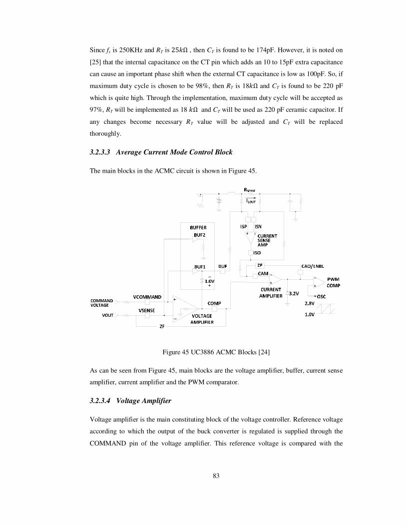
83
Since fs is 250KHz and RT is 25¼Ω , then CT is found to be 174pF. However, it is noted on
[25] that the internal capacitance on the CT pin which adds an 10 to 15pF extra capacitance
can cause an important phase shift when the external CT capacitance is low as 100pF. So, if
maximum duty cycle is chosen to be 98%, then RT is 18¼Ω and CT is found to be 220 pF
which is quite high. Through the implementation, maximum duty cycle will be accepted as
97%, RT will be implemented as 18 ¼Ω and CT will be used as 220 pF ceramic capacitor. If
any changes become necessary RT value will be adjusted and CT will be replaced
thoroughly.
3.2.3.3 Average Current Mode Control Block
The main blocks in the ACMC circuit is shown in Figure 45.
Figure 45 UC3886 ACMC Blocks [24]
As can be seen from Figure 45, main blocks are the voltage amplifier, buffer, current sense
amplifier, current amplifier and the PWM comparator.
3.2.3.4 Voltage Amplifier
Voltage amplifier is the main constituting block of the voltage controller. Reference voltage
according to which the output of the buck converter is regulated is supplied through the
COMMAND pin of the voltage amplifier. This reference voltage is compared with the

84
voltage of the voltage divider network at the output of the buck regulator through the
VSENSE pin. Voltage amplifier has 3.5MHz gain bandwidth and an open loop gain of
85dB. Accuracy of the voltage amplifier is optimized with an offset voltage as low as
±2mV and offset input current as low as ±0.01µA.
Voltage at the input of the COMMAND pin can be set using the VREF pin as shown in
Figure 46, since VREF pin has a 5V trimmed reference voltage produced by the IC itself.
Figure 46 Setting VCOMMAND [24]
The common mode voltage of the voltage amplifier is given as 3.0V. That’s why both the
VCOMMAND voltage and the VSENSE voltage are set to this voltage range. Considering
a small margin between these voltages, voltage at the COMMAND pin is adjusted to 3.1V
by setting R2 as 2.5¼Ω and R1 as 1.5¼Ω.
Controller network for the voltage loop will be build around this voltage amplifier using the
VSENSE and COMP pins. As mentioned above, VSENSE pin is the inverting input pin and
the COMP pin is the output of the voltage amplifier and it is also the non-inverting input of
the current amplifier. Basic implementation of the voltage controller network is as given in
Figure 35. Selection of the resistors and the capacitors constituting the voltage controller
are as given in Section 3.2.2.
3.2.3.5 Current Sense Amplifier
In order to measure and compare the inductor current with a reference, a measuring
resistance RSENSE is placed just after the inductor in series with it. Current measured
through the RSENSE resistor on the buck converter is measured and amplified by the
current sense amplifier in UC3886D. This current sense amplifier is placed in a differential
amplifier configuration so that only the difference voltage across the RSENSE is measured.
Configuration of the Current Sense Amplifier with the RSENSE is given in Figure 47.

85
Figure 47 Current Sense Amplifer Configuration [24]
In Figure 47, VISO is the output of the current sense amplifier and related with the buffer
voltage ,VBUF, and the voltage on the RSENSE resistor, VSENSE, as in (95).
¿%& = ÀÁÂ + JO2O1L%sy%s (95)
Ratio of R2 to R1 gives the gain of the current sense amplifier, GCSA. Current sense
amplifier has a common mode input voltage range of 0V-4.5V. Considering the fact that the
input voltage range of the specified buck converter is 25V-33V and the output voltage is
about 20V, then a voltage divider circuit will be built using R1 and R3 resistors. So, the
voltage level at ISP and ISN pins are held in the specified common voltage range of the
current sense amplifier.
Figure 48 Current Sense Amplifer with Voltage Divider Network

86
Assuming a voltage as high as 33V in the worst case around RSENSE, then the ratio of
R1/R3 is approximately 6. So, setting R3 as 5KΩ, R1 will be 30KΩ. Gain of the current
sense amplifier is adjusted by the ratio of R2/R1. Minimum gain of the amplifier is 5 and
the maximum gain is given as ;
GCSA_MAX=2.5MHz/fs and since fs is 250KHz for our application, GCSA_MAX equals
to 10 for this application. Considering the equation for the short circuit current;
-% × O%sy%s × (%- = 1 (96)
If the short circuit current (%- is set as 2 A, then -% × O%sy%s is found to be 0.5Ω. Setting -% as 6, O%sy%s is found to be 0.084Ω . Considering the power dissipation on the
RSENSE at nominal and short circuit conditions, these are found to be as 0.1W for Inom of
1.1A and 0.33W for Isc of 2A.
Then R2 is found from -% = R2/R1 which is approximately 180K.
3.2.3.6 Current Amplifier and PWM
Current Amplifier is the main block of the current compensation network. Necessary
compensation network elements are placed according to Subsection 3.2.2. Current amplifier
of the UC3886D has a 3.5MHz Gain Bandwidth and an open loop gain of 85dB. Current
amplifier compares the output of the voltage amplifier (COMP) and the output of the
current sense amplifier (ISO) in order to create a current voltage error.
Figure 49 Current Compensator, Voltage Controller and PWM configuration
In Figure 49, basic connections of the current amplifier and the PWM are given. Output of
the current amplifier (CAO/ENBL) is compared with the oscillator signal (OSC) which is in

87
the range of 1V-2.8V. According to this comparison, necessary PWM signals are produced
to turn on/off the MOSFET switch. Output of the current amplifier is clamped at 3.2V by
an internal Zener diode so that a fast transient response can be achieved during large
transient signal conditions.
3.2.3.7 Soft Starting of UC3886D
When a power supply is started up, initially the output voltage is zero. That’s why the error
on the voltage controller is at its largest value. So, the input switch MOSFET is driven at its
maximum rating until the output voltage is at its desired level. If the input supply has a
current limit, high current levels needed during the start up will result the input voltage to
decrease and the output voltage level will not be reached. In this condition, more current
will be tried to be driven by the MOSFET to compensate the low output voltage and as a
result in a latch condition at the input. In the same manner, if the output load is capacitive,
then large transient currents are required to charge the load and as a result high stress on the
MOSFET switch or on the driver section will cause a failure of the converter. Even if any
of the above cases are not encountered, a destructive overshoot and ringing at the output are
usually encountered if the supply is turned on suddenly.
In order to overcome these problems, power supply is needed to be turned on at a slower
rate in a controlled manner. This type of startup is called “soft starting”. With soft starting
output of the supply is raised slowly and so the initial error from the voltage controller is
decreased. As a result, need for high drive currents and the overall system stress is reduced.
Soft starting via UC3886D can be achieved by a capacitor connected to the COMMAND
pin. With this capacitor, the reference voltage (on the COMMAND pin) for the voltage
controller is not raised immediately but slowly. So, the error through the voltage controller
will be less and hence output voltage will be turned on at a slower rate. Addition of the soft
start capacitor is given in Figure 50.
Figure 50 Soft Start of UC3886 [24]

88
Resistor values for R1 and R2 have been chosen in Subsection 3.2.3.4. Adjusting the soft
start period for 50ms, the time constant τSS will be 10ms from (97) and (98).
Ã%% = H%% O1 × O2O1 + O2 (97)
:7;:/£ = 5 × Ã%% (98)
Since R2 is chosen as 2.5¼Ω and R1 as 1.5¼Ω, CSS is approximately 10µF for the specified
soft start period.
3.2.3.8 Driving the MOSFET Switch with UC3886D
UC3886D has a direct gate drive property to drive the high side N-Channel MOSFET
switch. In order to analyze the capability of the direct gate drive, circuit parameters such as
VIN, VCC, UVLO, the UC3886 totem-pole gate voltage and ringing voltages on the Gate
and Source nodes as well as the MOSFET Switch parameters such as VGSmin, VGSmax,
RDSon vs VGS should be evaluated [24]. Gate to Source voltage that the IC can supply is 7V
and the range for the gate to source voltage of the MOSFET Switch Si4484E is between
6V-10V. Also RDSon value of the Si4484E changes with the VGS value and it has a lower
value for VGS equal to 10V. Turn on time for the Si4484EY is also specified at a VGS value
for 10V and driving the MOSFET with a lower value will cause a delayed turn on of the
MOSFET.
More important than the above issues is the driving the N-MOS in a high side
configuration. When driving an N-MOS, gate voltage of the MOSFET should be at least
10V-15V higher than the drain voltage [26]. However, drain of the MOSFET is directly
connected to the input voltage in a high side configuration and input voltage is the highest
voltage of the overall system. Gate voltage of the IC is referenced to ground, however, in
the high side configuration the source of the MOSFET swings between two rails of the
system and hence the reference of the gate voltage from the IC shall be adjusted [26].In
order to drive an N-Channel MOSFET on the high side, bootstrap technique can be used.
This technique is used for the specially designed driver ICs and an example can be seen as
given in Figure 51 [27].

89
Figure 51 Bootstrap Driving
An external capacitor CBS and an external diode DBS are used to form the bootstrap circuit.
When the low side switch (either a MOSFET or a diode) is on and the high side MOSFET
is off, CBS is charged through the DBS from the input supply (VCC) and the source voltage
of the high side switch is pulled down to ground. When the PWM signal goes high, high
side MOSFET begins to turn on using the charge on the CBS. Then the source of the high
side switch rises up to the logic input voltage level of the IC and as a result enough gate to
source voltage is kept on the switch. For the bootstrap circuit selection of the capacitor and
diode are the key features.
The bootstrap capacitor shall have a voltage rating that is able to handle the maximum input
voltage plus a margin of at least 5V. So, for the designed circuit the capacitor shall have a
voltage rating of at least 50V. The minimum capacitance of the CBS can be determined
using the formula;
HÀ% = G+R∆À% (99)
Where QTotal is the total gate charge composed of Qg, ICbs (leak), Iqbs(max) and Qls where
Qg is the gate charge of high-side FET, ICbs (leak) is the bootstrap capacitor leakage
current (only for the electrolytic capacitor), Iqbs (max) is the maximum VBS quiescent
current and Qls is the level shift charge required per cycle. In (105), ∆À% is the voltage
drop allowed on the high side MOSFET.

90
G+R = 2 × (2 × G3 + GR5 + (-Ä5(R*+,) + (ÅÄ5;56 )∆À%
(100)
In the same manner, the bootstrap diode should be able to block the voltage at the supply
line of the converter and its current rating is equal to the switching frequency multiplied by
the gate charge of the MOSFET. Also, it should have a fast recovery time (<100ns) to
reduce the amount of charge that is fed back from the bootstrap capacitor into the supply
So driving the MOSFET Switch, Si4484EY, directly by the UC3886D is not possible.
That’s why the gate drive output of the IC will be used as an input for an additional gate
drive IC. LM5104 HV Floating MOS-Gate Driver IC from National Semiconductor is
selected for synchronous buck operation.
LM5104 is capable of driving both the high side and low side MOSFET switches, which
makes it suitable for synchronous buck converter applications. It has a single input and a
bootstrap supply voltage range up to 118V. It has a maximum gate drive voltage of 12V
which is within the limits of the Si4484E requested gate voltage. The recommended supply
voltage (VDD) range of the IC is 9V-14V.
Output from the GATE pin of the UC3886D is fed to LM5104 via a voltage divider since
the output and input voltage ranges of the two ICs are different. Output voltage levels for
UC3886D are given as maximum 2.2V for output low voltage and minimum 9V for output
high voltage. Input voltage threshold level for the LM5104 is 0.8V for low level and 2.2V
for high level. So, using a 1/3 voltage divider network ensures that the output voltage levels
of UC3886D is suitable for LM5104. Also, bootstrap component values are calculated
according to (99) and (105) for 250 KHz switching frequency and;
Qg =30nC for Si4484E (101)
ICbs (leak) = 0 due to using a ceramic capacitor (102)
Iqbs (max) = 0.2mA for LM5104 (103)
Qls = 5nC for LM5104 (104)

91
∆VBS =0.1V (105)
Then G+R is found to be approximately as 1.3uF. So using a ceramic capacitor of 1.5uF
with a voltage rating of at least 5V to 10V more than the maximum supply voltage is
suitable. For the bootstrap diode, the minimum DC block voltage is 33V and the current
rating is 7.5mA from the product of the total gate charge on the MOSFET and the switching
frequency. As the bootstrap diode 50SQ100 from International Rectifer is used with 100V
DC block voltage and forward voltage drop of 0.52V.

92
CHAPTER 4
5. EXPERIMENTS
In this chapter, simulation results, test procedure and test results of the experiments that
have been conducted on the hardware are explained. Firstly, simulation results of the
proposed system are introduced and necessary discussions on these results are given.
Following this, test procedure for the power stage is explained. Next, test set-up including
the hardware manufacturing details is given. Then test results obtained throughout the tests
are demonstrated.
4.1 Simulations
Simulations of the buck regulator which is the main constituting block of the power stage
have been conducted using Simplorer Simulation Center 7.0. In Figure 52, schematic
representation of the buck converter is given.
In the schematic, main blocks for the ACMC are constructed using separate op-amp
configurations taking into account of the UC3886D configuration. Also, buck converter
configuration is simulated as non-synchronous since main aim is to obtain a stable
converter with the desired regulation and there is no difference between a non-synchronous
and synchronous converter during the simulation in terms of stability and regulation.
During the simulations, current sense amplifier is simulated using the current on Rsense and
multiplying its value by the gain block. This multiplication is fed to the Gca, the current
amplifier. In order to simulate the soft start function of the ACMC IC, VCOMMAND is adjusted
by the DATAPAIRS1 and it reaches the reference value of 2V after 1msec. Soft start
duration is set at a lower value than that of the calculated value to have a fast simulation.

93
Figure 52 Buck Converter Schematic
Power stage component values are given in Figure 52 and control loop parameters are given
in Subsection 3.2.3.4 and Subsection 3.2.3.5. In Figure 52, output voltage of the converter
is given for Vin=28V and Rout=20Ohm.
Figure 53 Vout for Vin=28V and Rout=20Ohm

94
Figure 54 Settling Time for Vout for Vin=28V and Rout=20Ohm
From Figure 53 and Figure 54 it is seen that the converter is able to produce 20V output
voltage. Settling time for the output voltage is approximately 10msec. Also, there is a slight
voltage overshoot of 30mV. It is possible to speed up the control loop by increasing the
bandwidth. However, in this case, there is a risk of losing stability due to oscillations.
Since, stability is the determinant factor and the transient response of the control loop is
fairly enough, there is no need for bandwidth extension.
Figure 55 Output Voltage Ripple

95
In Figure 55, output voltage ripple for Vout is shown. Output voltage ripple is
approximately 20mV peak to peak, which is smaller than 0.1%.
Figure 56 PWM Output (R8.V)
Figure 56 shows the waveform on R8 which is the PWM controller output. Duty cycle is
approximately 0.722 which is very close to the calculated value of 0.714 for Vin=28V and
Vout =20V.
Figure 57 Voltage Waveforms for SW1 and Dfw via VM2.V (Green Line) and VM3.V(Red
Line) respectively

96
Figure 57 shows the voltage waveforms on SW1 and Dfw. Since MOSFET is simulated
using a body diode, waveforms are offset at 0.8V for SW1 and 0.3V for Dfw. It is seen that
SW1 and Dfw are on at the same time for a short duration. This issue should be handled
implementing a delay in the gate driver, LM5104, in order not to cause shoot-through in the
hardware where freewheeling diode is replaced with a MOSFET for synchronous operation.
Otherwise, driver will try to open both switches at the same time resulting in a over current
condition.
In Figure 58, Thermal Knife resistance during firing is simulated and load current is
observed. Load resistance is changed between 20 Ohm and 12 Ohm with 1 Ohm steps
within 0.2 msec. In the figure, load resistance, DATAPAIRS3, is scaled to 1/10 for best
representation.
Figure 58 Output Current (Red Line) during Output Load Change (Blue Line)
During firing, the converter is supposed to supply 1A current to the Thermal Knife the
resistance of which changes approximately between 20 Ohm and 11.5 Ohm.

97
Figure 59 Zoomed View for Output Current (Red Line) during Output Load Change (Blue
Line)
As seen from Figure 59, load resistance is scaled to 0.7 and output current is at 1.01A.
There is a current rise of approximately 0.065A during the step load changes. It can be
possible to speed up the controller a bit more but this is not necessary since the change is
small and recovery is fast.
Another test parameter is the input voltage change. In Figure 60, change of input voltage
from 28V to 25V and to 33V is represented. Voltage change is performed within 1msec and
in Figure 60, input voltage is represented as DATAPAIRS2. As seen from the figure, there is
no visible change in the output voltage and it is well regulated at 20V. Same result is
obtained from Figure 61 and Figure 62; change in the output voltage is almost invisible.
This situation is the characteristic of current mode control. Since any change in the input
voltage is tracked through the average inductor current by the current loop, it can be
compensated before it is introduced to the output voltage. So, a very fast transient response
is obtained in terms of input voltage change.

98
Figure 60 Input Voltage Change (Blue Line) and Output Voltage Response (Red Line)
Figure 61 Input Voltage Change from 28V to 25V (Blue Line) and Output Voltage
Response (Red Line)

99
Figure 62 Input Voltage Change from 25V to 33V (Blue Line) and Output Voltage
Response (Red Line)
Stability of the converter at different output voltages are viewed in Figure 63and Figure 64.
When two waveforms are compared, it is seen that output voltage at 25V input voltage
begins to lose regular form and it contains sub harmonic oscillations. This is due to the
increasing duty cycle and excess phase shift in the PWM controller due to increasing gain
of the control loop.
Figure 63 Output Voltage Ripple at Vin=25V

100
Figure 64 Output Voltage Ripple at Vin=33V
Adding slope compensating solves the subharmonic oscillation problem and the converter
stability increases. However, subharmonic oscillations at 25V input voltage is not excessive
and the supply of the converter is a well regulated 28V of the PDU of the spacecraft. So,
slope compensation is not needed in this case.
4.2 Test Procedure and Test Results
During the hardware testing of the buck converter, power stage circuit of the converter and
the control stage of the converter are tested separately at the beginning. After necessary
adjustments performed on each stage two circuits are connected together and an overall
performance test is performed.
The test equipments used are given in Table 8.
Table 8 Test Equipments
Name-Model Specifications
Power Supply- Amrel SPD120-3-KDE-1 Dual Output, 120V-3A-360W
Digital Load- HP 6050A Dual Output 1800 Watt
Function Generator –HP 33120A 15Mhz, 0.8 Duty cycle

101
Digital Load- Amrel LPL 600-120-60 120V-60A-600W
Oscilloscope Textronix TDS 5104
Figure 65 Experimental Test Set-up
Top and bottom views of the implemented power stage circuitry are given in Figure 66
respectively.
Figure 66 Power Stage Circuitry Top and Bottom Views Respectively

102
4.2.1 Power Stage Tests
Power stage tests have been conducted with the power supplies from Agilent Technologies.
Input voltage is adjusted at 28V and the source voltage for the LM5104 is adjusted as 12V.
In order to observe gate drive pulses of the LM5104, a function generator is used as PWM
controller. Output of the function generator is connected to the IN pin of the driver.
Frequency of PWM pulses are adjusted to 250 kHz and the voltage level is set to 5V peak
to peak. Duty cycle is set at 0.72 to obtain 20V output.
In Figure 67, timing of the output high and output low pins of the driver are shown. CH1
shows the PWM input from the function generator, CH2 shows the low side output,LO, and
CH3 shows the high side output, HO. As can be seen from the waveforms, there is a delay
between the rising of the PWM pulses and the rising of the high side gate pulse. Also same
delay occurs between the low side gate drive pulse rise and the falling edge of the PWM
pulse. This delay is necessary to overcome shoot-through of the MOSFETs. However,
MOSFET capacitances do not charge and discharge fast enough and eventually they stay
open at the same time during the switching.
Figure 67 PWM Pulses (CH1-Yellow), LO (CH2-Blue) and HO (CH3-Purple) Outputs
In order to overcome the shoot-through problem, gate resistances of the MOSFETs are
changed from 24ohm to 12 ohm. Resulting waveforms are given in Figure 68.

103
Figure 68 LO (CH2-Blue) and HO (CH3-Purple) Outputs with Rgate=12Ohm
Figure 69 Closer View for LO (CH2-Blue) and HO (CH3-Purple) Outputs with
Rgate=12Ohm
As seen in Figure 68 and Figure 69, changing the gate resistances have eliminated the
shoot-through problem. There is approximately a delay of 128 ns between the gate drive
pulses.

104
Figure 70 Freewheeling Diode Waveform
In Figure 70, voltage waveform on the freewheeling diode is given. It is seen that there is
some noise on the waveform due to the PCB layout and soldering.
In Figure 71, output voltage waveform is given. It is seen that output voltage is in the range
of 20V as simulated with CH3 Volt/div set at 10V.
Figure 71 Output Voltage Waveform (20V) for Vin=28V

105
With the open-loop test of the power stage it is observed that the designed converter has an
output regulation for 20V as desired. There is no shoot-through with smaller gate resistance
values and no remarkable voltage drop due to components.
4.2.2 Control Stage Tests
For the control stage test of the buck converter, UC3886 ACMC IC is supplied via 12V and
its GATE pin waveform is observed. Since this pin is the actual PWM input for the
LM5104 gate driver, it is important to obtain variable PWM pulses within the specified
voltage limit of the driver.
First of all sawtooth waveform from the oscillator output of the UC338D is observed to see
if it is between the set limits. Observed waveform is given in Figure 72.
Figure 72 Sawtooth Voltage Waveform (CH3-Purple)
As seen from Figure 72, sawtooth waveform has a maximum voltage of 2.8V and 0.88mV.
In the datasheet of UC3886D, the voltage range is given as 2.8V-1.0V and the difference is
due to the measurement of the oscilloscope which is prone to noise.
From Figure 73 to Figure 76, PWM pulses generated by the UC3886D are observed for
different voltage levels. During this test, since the power stage is disconnected, reference
voltage fed to the IC through the SENSE pin is varied between 1.92V and 1.97V to
represent the small variations on the output voltage. Since the voltage change is performed

106
manually, duty cycle is fixed due to the absence of feedback. As seen from the following
figures, PWM output and hence the duty cycle changes between 0.85 and 0.10 for various
reference voltages. So, it is concluded that the ACMC IC is capable of producing a variable
PWM output for changing output voltages.
Figure 73 PWM pulses (CH4-Green) for VSENSE=1.922V
Figure 74 PWM pulses (CH4-Green) for VSENSE=1.945V

107
Figure 75 PWM pulses (CH4-Green) for VSENSE=1.963V
Figure 76 PWM pulses (CH4-Green) for VSENSE=1.972V
4.2.3 Overall System Tests
As mentioned at the beginning of Section 5.2, after desired results are obtained from the
individual tests of power stage and the control stage of the buck converter an overall system
test is performed to evaluate the performance of two separate system together. Overall

108
system tests are performed by connecting the power stage and the control stage together.
Output of the control stage, the PWM signals, is used to control the power stage. Since
variable PWM generation for variation in the output voltage is observed during the control
stage tests, it is expected that control stage is able to regulate the output voltage despite of
variations in the input voltage, output voltage and hence the output resistance.
In Figure 77 output voltage waveform is given for Vin=28V and Rout=200Ohm which is
the situation before firing of the thermal knife. As seen from the figure, output voltage is at
20V desired with CH4 Volt/div set at 10V.
Figure 77 Output Voltage for Vin=28V and Rout=200Ohm
In Figure 78, PWM waveform for 28V input and 20.7V output are observed with an
operating frequency of approximately 235kHz. Duty cycle is about 0.77, a little higher than
the calculated duty cycle of 0.714. This can be due to the voltage drop on the components
which are undervalued during calculations.
Also, there seems a ringing approximately 340ns after the rising edge of the PWM
waveform. A closer observation for the ringing pulse is given in Figure 79.

109
Figure 78 PWM waveform (CH4-Green) for Vin=28V and Vout=20Ohm
Figure 79 Zoomed View for the Ringing in the PWM waveform (CH4-Green)
As seen from Figure 79, ringing dies out in 160ns and it has a magnitude of approximately
2.5V. Since the ringing is not introduced on the rising edge of the PWM and it occurs after
320ns, it seems to be a reflection of noise coupling or ringing in somewhere else in the
system. The most common ringing source of the synchronous buck converters, the
MOSFETs in the power stage, are also observed. The waveform on the freewheeling diode
across low side MOSFET is given in Figure 80 and Figure 81.

110
Figure 80 Waveform of the Freewheeling Diode (CH4-Green)
Figure 81 Zoomed View for the Ringing in the Freewheeling Diode (CH4-Green)
As can be seen from Figure 80 and Figure 81, low side switch freewheeling diode has a
ringing on the rising edge of its waveform. The ringing dies out in roughly 50nsec and it
has a magnitude of 10V. This ringing is usually caused by the reverse recovery of the body
diode of the low side MOSFET [65]. Ringing on the rising edge of the high side MOSFET
is usually caused by the RLC tank circuit formed by the ESR and ESL of the input
capacitances, MOSFET capacitances and trace inductances. In order to overcome this
problem, a good PCB layout should be formed. Minimizing the node length between the
input capacitor and the high and low side MOSFETs [66] are offered for reducing the trace

111
parasitic and the loop area. Also, inserting a resistance in series with the bootstrap capacitor
is offered for filtering the ringing [65].
In Figure 82 and Figure 83 high and low side switches gate drive pulses are shown.
Figure 82 Delay between High Side (CH4-Green) and Low Side (CH1-Yellow) Switch
Drive Pulses
Figure 83 Delay between Low Side (CH1-Yellow) and High Side (CH4-Green) Switch
Drive Pulses

112
In the above figures it is seen that, there is no shoot through problem for the high and low
side gate drive pulses and in fact there is a delay of 96ns between the operations of two
switches.
The measurement for the transient response of the system for the output rise during the
initial switch on of the system is given in Figure 84 and Figure 85. CH1 represents the
output current and CH3 represents the output voltage.
Figure 84 Output Voltage (CH3-Purple) Rise from 0V to 20V and Output Current (CH1-
Yellow) Rise from 0A to 200mA
Figure 85 Output Voltage (CH3-Purple) Rise from and Output Current (CH1-Yellow) Rise

113
In the figures it is seen that Vout rises from 0V to 20V in 4msec for Vin is switched on from
0V to 28V and Rout=100Ohm. Output current reaches to 200mA in approximately
12msec.The difference between the settling times of the output voltage and current is
possibly due to using a separate current probe for current measurement.
In Figure 86, output current and voltage changes are given for Rout changing between 200
Ohm and 20 Ohm with a period of 0.1sec. As can be seen from the figure, although the
output current rises from 100mA to 1A, output voltage does not change significantly. In
fact the change in the output voltage is below 1V and since at a load resistance of 200 Ohm,
output voltage is approximately 20.7V, this slight voltage drop keeps the output voltage in
the safe limits of 18.5V-21.5V for the thermal knife.
Figure 86 Output Voltage (CH4-Green) and Current (CH1-Yellow) Waveforms for Rout
Change from 200Ohm to 20Ohm
In Figure 87, output voltage and current waveforms are observed for Rout changing
between 22 Ohm and 12 Ohm with a period of 0.2msec. It is observed that output current
rises from 900mA to 1.2A during the transition from 22 Ohm to 12 Ohm and the output
voltage is no more kept at 20V. So, step down converter begins to operate in the constant
current mode rather than the constant voltage mode which is the case for Rout greater than
20 Ohm. Efficiency of the power stage at this stage is approximately 78% for Rout equals
10 Ohm and 94% for Rout equals to 20 Ohm, hence an average of 90% of efficiency is

114
achieved. So, it is guaranteed that during firing, while the resistance of the thermal knife
changes between 10 Ohm and 20 Ohm, a nominal output current of 1A can be supplied
with high efficiency.
Figure 87 Output Voltage (CH3-Purple) and Current Waveforms (CH1-Yellow) for Rout
Change from 22Ohm to 12Ohm
Output current tends to raise a bit more as the load resistance decreased further. This is due
to the low gain of the current sense amplifier. In the calculations, gain has been calculated
as 9 and raising the gain slightly above this value will solve the problem. This is because,
when the gain is higher the current compensator input becomes higher too and hence
control loop tends to raise the output voltage less than usual. As a result, less current is
introduced to the output. Increasing the gain of the current sense amplifier may decrease the
20V output voltage when Rout is higher than 20Ohm. However, since output voltage is
slightly higher than 20V this is not a crucial issue.
115
CHAPTER 5
6. CONCLUSIONS
7.
This chapter begins with the summary of the work performed for the Power Stage of a
Deployment Mechanism Driver that is designed. In the second section of this chapter,
remarks on the experimental work and its results are given. In the last chapter, possible
improvement strategies on the design and on the component selection are discussed.
5.1 Summary
Deployment mechanism drivers enable a controlled initiation of deployment by supplying a
well regulated and controlled DC power input to deployment mechanism actuators through
its power stage and by monitoring the power stage and the actuators through its control
stage.
There are several different deployment mechanism actuator types with different current and
voltage inputs, but the main requirement for the input supply for these actuators to provide
well regulated and well controlled power. Although it is possible to supply necessary power
to the deployment mechanism actuators directly by the battery block of the spacecraft or by
the Power Distribution Switches without using a separate power stage in order to reduce the
cost, weight and complexity of the overall system, such an application introduces many
risks which decreases the reliability and safety of the system and whole spacecraft. Even,
complete mission loss can be encountered due to unsuccessful deployment phases as a
result of actuator wear out during the mission, overvoltage/overcurrent or
undercurrent/undervoltage occasions, spacecraft power system loss, etc which are the most
probable results of varying power levels at the input of the actuators. Hence, design of a
separate power stage with well controlled and regulated output is a solution to reduce the
risk level and to increase the reliability and safety of the deployment and the mission itself.

116
This thesis presents the power stage of a deployment mechanism driver which performs
voltage regulation and current control using the battery block unregulated voltage or the
spacecraft bus voltage. The designed power stage is capable of producing a well regulated
DC voltage and controlled DC current input for thermal knife actuator. Thermal knife
actuator is selected as the load of the power stage in order to be able to define and limit the
power stage design requirements. Among many actuator types, thermal knife (MHRM)
actuator is selected due to its many advantages such as overall system cost saving, low
shock profile, no risk of spontaneous operation, etc.
In the power stage, voltage regulation is performed using a Step Down DC/DC Converter.
Step down converter has high efficiency and it is easy to analyze and implement which is
important for space applications where simple and so more reliable, cost saving and
efficient solutions are preferred. For the constant current control, Average Current Mode
Control method is selected since it enables to put a limit on the output current, it has high
noise immunity and stability which are also important to obtain a well regulated output.
Hence, using a Step Down Converter with Average Current Mode Control, a compact and
yet simple, efficient power stage is obtained to provide well regulated and well controlled
voltage and current according to the requirements of the thermal knife. Yet, it is possible to
modify the designed power system according to the needs of other actuators since step
down converter with ACMC method is easy to adapt for different voltage and current
ratings.
5.2 Discussions
In this thesis, a step down converter with average current mode control method is designed
and implemented as the power stage of a deployment mechanism driver. Output voltage
regulation and current limiting capability are tested and verified using simulations and tests.
Power stage is designed and tested for an input voltage range of 28V±5V which is the
general voltage range of a spacecraft battery of 28V nominal output. Voltage regulation to
20V is tested for load resistance greater than 20 Ohm and current limiting to 1A is tested
for load resistance smaller than 20 Ohm. Such a load resistance change is a characteristic of
thermal knife actuator the resistance of which increases from approximately 10 Ohm to 22
Ohm due to heating during deployment. Power stage of the step down converter and the
control stage of the step down converter are tested separately and then an overall system

117
test is performed connecting two stages together. The power stage works successfully and it
has a well voltage regulation and current limiting in line with the operational requirements.
During the power stage tests that are given in Subsection 4.2.1, the major problem that is
encountered is the shoot through problem of the high side and low side MOSFET switches
of the power stage. Shoot through problem occurs due to synchronous operation of the
power stage using these two MOSFET switches. In normal operation of the synchronous
step down converter, while one of the switches is in conduction the other one stays off and
the off switch does not begin conduction until the other one completely turns off. Despite
the fact that MOSFET gate driver IC, LM5104 is implemented introducing a delay between
the switch turn on and turn off periods, during the tests it is seen that both switches are in
conduction for a approximately 300ns and this duration is high enough to cause failure of
the driver, LM5104 or if such a failure is not the case, then efficiency and regulation of the
converter is greatly reduced. In order to overcome this problem, gate resistances of the
MOSFETs are reduced from 24 Ohm to 12 Ohm in order to speed up the charge and
discharge of the MOSFET capacitances. Performing the tests once more with new gate
resistances, it is seen that enough delay between operation of the switches are obtained.
Delay time is approximately 128ns which eliminates the shoot through problem. Apart from
the shoot through problem, it is observed that power stage of the step down converter
performs 20 output voltage regulation perfectly for the given input voltage range.
While performing the control stage tests, the major difficulty that is encountered is to obtain
a variable duty cycle from the output of the ACMC IC, UC3886D. In order that the power
stage of the deployment mechanism driver performs voltage regulation to 20 V for different
input voltages, controller of the step down converter is to be able to produce the necessary
duty cycle according to the supplied input voltage level. During the tests, it is seen that duty
cycle of the controller IC is fixed at 0.97 so, it is not possible to obtain a 20V output voltage
for even a 28V input. A possible reason of such an incident is due to exceeding the gain
bandwidth product of the amplifiers for the set gain and switching frequency. To overcome
this problem, gain and stability analysis of the converter is performed once more.
Afterwards new component values for the control loop are obtained and tests are performed
and variable duty cycle characteristic is obtained successfully. So, it is important to perform
a careful design on the current loop so that controller IC requirements and calculated
component parameters match.

118
After obtaining the desired results from each stage separately, power stage and the control
stage of the step down converter are connected together and an overall test is performed.
The apparent problem during the overall system tests, is the ripple/ringing seen on the
MOSFET switches rising edges and on the PWM pulses of the ACMC IC output. The
ringing on the PWM has a reflected type characteristic, but since it dies out immediately
and does not have a significant magnitude it is not a major problem. Also, since MOSFET
switches have a high voltage rating the ripple during turn on is not a critical issue. Placing
power stage components such as the output and input capacitors and the inductor closer and
minimizing the trace lengths between the input capacitors and the MOSFET switches help
to reduce the problem. Since such an improvement requires new PCB design and
manufacturing it is left as a future work.
As a result, it is observed that for a load resistance greater than 20 Ohm, step down
converter with ACMC is able to produce a well regulated 20V output for 28V±5V input
voltage. When the load resistance is smaller than 20 Ohm, step down regulator performs
current limiting successfully approximately at 1A±200mA. Such a margin is quite
acceptable for the 1A nominal operation voltage of the thermal knife..Also, designed power
stage has an efficiency of approximately 90% which shows that the designed power stage is
successful when efficiency requirement is considered.
5.3 Future Work
PCB layout design can be reworked in order to reduce or eliminate any issue related with
ripples or noises during the system operation. Also, after the prototype work for the
designed system is completed, PCBs for engineering and flight models shall be
manufactured according to space qualification standards by qualified manufacturers. This
help to improve system performance and increase reliability and safety.
In order to increase the reliability and reduce the risk of single point of failure, external
protection circuitries such as input current limiters for spacecraft bus power protection and
output activation switches for actuator protection can be included. One type for the possible
solution of the input current limiter is given in APPENDIX B as basic information.
Detailed analysis and design for the current limiter and output activation switches shall be
performed to obtain a reliable and safe operation.
Any failure on the power stage results in unsuccessful deployment and hence spacecraft
mission is endangered. In order to increase the reliability level and avoid single point of

119
failure, redundancy design can be performed. For reliability, either critical components can
be placed as redundant or the whole power stage of the deployment mechanism driver can
have full redundancy. Such a reliability work will be conducted for engineering and flight
models.
Current limiting capability of the designed circuitry can be improved by using more
sensitive current sense resistors. Since the gain of the current sense amplifier is limited due
to the voltage divider network constructed around the current loop to keep the common
mode operating voltage within the limits, increasing the current sense resistor value in
small portions can help to adjust the limitation. Such resistor values are hard to obtain
among the off the shelf products. So, for engineering or flight model manufacturing, these
resistors can be ordered in various values with enough manufacturing and delivery time.

120
8. REFERENCES
[1–29] [30–32] [33–70]
[1] R. W. Erickson, “DC–DC power converters,” Wiley Encyclopedia of Electrical and
Electronics Engineering, 1998.
[2] M. Santos, H. Ribeiro, M. Martins, and J. Guilherme, “Switch Mode Power Supply Design Constraints for Space Applications,” ConfTele2007, pp. 157–160, 2008.
[3] “Linear regulator - Wikipedia, the free encyclopedia.” [Online]. Available: http://en.wikipedia.org/wiki/Linear_regulator. [Accessed: 20-Nov-2011].
[4] N. Mohan, T. M. Undeland, and W. P. Robbins, Power Electronics: Converters,
Applications, and Design. John Wiley & Sons, Inc., 2003, p. 824.
[5] M. S. Rahman, “Buck Converter Design Issues,” Division of Electronic Devices
Linkopings University, 2007.
[6] “Analysis of Buck Converter.” [Online]. Available: http://encon.fke.utm.my/nikd/SEM4413/AnalysisConverter-buck.pdf. [Accessed: 15-Jun-2011].
[7] T. Texas Instruments, “Understanding Buck Power Stages in Switchmode Power Supplies Application Report,” 1999.
[8] R. W. Erickson, Fundamentals of Power Electronics. Kluwer Academic Publishers, 2002, p. 900.
[9] C. Ellison, “Simple Synchronous Buck Converter Design - MCP1612,” Microchip
Technology Inc. Application Note, pp. 1-6, 2005.
[10] “Designing A Buck Converter from Scratch Part 1.” [Online]. Available: http://www.s4wsbox.com/?q=node/40. [Accessed: 14-Feb-2007].
[11] S. Maniktala, “Selecting Inductors for Buck Converters,” Texas Instruments,
Application Note, 2002.
[12] D. Schelle and J. Castorena, “Buck-Converter Design Demystified,” Power
Electronics Technology, no. June, 2006.
[13] On Semiconductor, “Switch Mode Power Supply Reference Manual,” 2002.
[14] On Semiconductor, “Switched Mode Power Supply Reference Manual and Design Guide,” 1999.

121
[15] Maxim Integrated Products, “Power Supply Engineer ’ s Guide to Calculate Dissipation for MOSFETs in High-Power Supplies,” Application Note, no. 1, 2002.
[16] S. Maniktala, Switching Power Supplies A to Z. Newnes, 2006, p. 528.
[17] “Spacecraft Bus Subsystems.” [Online]. Available: http://lr.tudelft.nl/index.php?id=29328&L=1. [Accessed: 10-Jun-2011].
[18] P. A. Jones and B. R. Spence, “Spacecraft Solar Array Technology Trends,” in Aerospace Conference, Proceedings., IEEE, 1998, vol. 1, pp. 141–152.
[19] P. Höhn, “Design, Construction and Validation of an Articulated Solar Panel for CubeSats,” Department of Space Sciences,Lulea University of Technology, p. 69, 2010.
[20] M. H. Lucy, R. C. Hardy, E. H. Kist, J. J. Watson, and S. A. Wise, “Report on Alternative Devices to Pyrotechnics on Spacecraft,” NASA Langley Technical
Report Server, 1996.
[21] R. Sheehan, “A New Way to Model Current-Mode Control,” Power Electronics
Technology Magazine, no. June, pp. 14–20, 2007.
[22] G. Levin and K. O’Malley, “Designing with hysteretic current-mode control,” EDN,vol 39, p. 95(6)-101, 1994.
[23] J. Klein, “Synchronous buck MOSFET loss calculations with Excel model,” Fairchild Semiconductor Application Notes AN-6005, pp. 1-7, 2006.
[24] L. Spaziani, “The UC3886 PWM Controller Uses Average Current Mode Control to Meet Transient Regulation Performance of High End Processors,” Texas
Instruments, Application Note U-156, 1999.
[25] L. Spaziani, “Fueling the megaprocessor-a dc/dc converter design review featuring the UC3886 and UC3910,” Texas Instruments, Application Note U-157, 1999.
[26] “HV floating MOS-gate driver ICs,” International Rectifier Application Note
AN978-b, no. International Rectifier Co., El Segundo,CA, 2003.
[27] “Application Note for LDIP-IPM,” Cyntec CO.,LTD, no. 46.
[28] M. Patel, Spacecraft Power Systems. CRC, 2005.
[29] A. Hyder, R. Wiley, G. Halpert, D. Flood, and S. Sabripour, Spacecraft Power
Technologies. London:Imperial College Press, 2000.
[30] S. We-pd and A. M. Abmessungen, “7445920-WE-PD-3 Choke,” Elektronik, no. 0. Datasheet, Würth Elektronik, pp. 1-3, 2004.
[31] C. Electriques, E. T. Climatiques, and C. Characteristics, “CTC21E Tantalum Capacitor Series,” Notes. Datasheet, FIRADEC, pp. 9-12.

122
[32] ECSS, “Space product assurance,” ECSS_Q_ST_30_11C_rev1, no. October, pp. 1-71, 2011.
[33] K. Köble, “Satellite Structures,” Small Satellite Design, 2003.
[34] J. Murray, A. Mignon, C. Promper, R. Stalmans, and R. Lanfranconi, “A Shape Memory Alloy Actuated Satellite Isolation Valve,” Proceedings of the 4th
International Spacecraft Propulsion Conference (ESA SP-555). 2-9 June, 2004,
Chia Laguna (Cagliari), Sardinia, Italy, p. 67.1.
[35] “Chapter 11-Typical Onboard Systems,” Basics of Space Flight Section II. [Online]. Available: http://www2.jpl.nasa.gov/basics/bsf11-4.php. [Accessed: 30-Dec-2011].
[36] “Thermal Knife,” Dutch Space. [Online]. Available: http://www.dutchspace.nl/pages/products/content.asp?LangType=1033&id=258. [Accessed: 20-Dec-2011].
[37] “SAX:Structure Subsystem.” [Online]. Available: http://www.iasfbo.inaf.it/extras/Research/SAX/Mission/subsy_str.html. [Accessed: 02-Jan-2012].
[38] F. Spoto et al., “Preparing MetOp for work-launch, early operations and commissioning,” ESA bulletin, vol. 127, pp. 24–30, 2006.
[39] E. Filippi and H. Attouman, “PYROSHOCK SIMULATION USING THE ALCATEL ETCA TEST FACILITY.,” Launch Vehicle Vibrations. First European
Conference.CNES Toulouse, Dec. 14-16, 99, pp. 1-12.
[40] Bement Laurance J, “Pyrotechnic System Failures: Causes and Prevention,” NASA
TM 10063.
[41] J. Cuttino, D. Newman, J. Gershenson, and D. Schinstock, “A structured method for the classification and selection of actuators for space deployment mechanisms,” Journal of Engineering Design, vol. 11, no. 1, pp. 31–53, 2000.
[42] T. R. McBriney, “Mechanical Actuator Assembly,” U.S. Patent US6192684.
[43] W. Shapiro, F. Murray, R. Howarth, and R. Fusaro, “Space Mechanisms Lessons Learned Study Volume I-Summary,” NASA Technical Memorandum 107046,
National Aeronautics and Space Administration, 1995.
[44] “Shape Memory Alloys,” TiniAerospace,Inc. [Online]. Available: http://www.tiniaerospace.com/sma.html. [Accessed: 02-Jan-2012].
[45] W. Huang, “Shape memory alloys and their application to actuators for deployable structures,” Diss. University of Cambridge, 1998.
[46] T. Konink and G. Kester, “MULTIPURPOSE HOLDDOWN AND RELEASE MECHANISM (MHRM),” The 13th European Space Mechanisms and Tribology
Symposium ,ESTMAS, vol. 2009, no. September.

123
[47] J. Cremers, E. Gooijer, and G. Kester, “MULTIPURPOSE HOLDDOWN AND RELEASE MECHANISM (MHRM),” in ESA-SP, Vol 438, 1999, p. 329.
[48] R. Zwanenburg, “The qualification test programme of the ENVISAT solar array mechanism,” in Sixth European Space Mechanisms and Tribology Symposium,
Proceedings of the conference held 4-6 October, 1995 in Zürich, Switzerland.
Edited by W.R. Burke. ESA SP-374. European Space Agency, 1995., p.65.
[49] “1/4" SN9423-2 Series,” Datasheet,Hi-Shear Technology Corp., 2006.
[50] “SP-5025 HOP Actuator,” Datasheet, STARSYS Research.
[51] “TiNi Standard Pinpuller Selection Guide,” TiNi Aerospace,Inc. [Online]. Available: http://www.tiniaerospace.com/pps/ppstandard.html. [Accessed: 02-Jan-2012].
[52] “MHRM Multipurpose Hold-down and Release Mechanism,” Productsheet, Dutch
Space.
[53] “High Power Command Card.” [Online]. Available: http://sm.mdacorporation.com/pdf/hpcc.pdf [Accessed: 15-Jan-2012].
[54] B. Jackson, “XMM’s Electrical Power Subsystem,” ESA Bulletin, vol. 100, pp. 59-63, 1999.
[55] V. A. Likhachev, A. I. Razov, A. G. Cherniavsky, Y. Kravchenko, and S. N. Trusov, “Truss Mounting in Space by Shape Memory Alloys,” in Proceedings of the First
International Conference on Shape Memory and Superelastic Technologies,
California, USA,, 1994, pp. 245-248.
[56] J. Bouwmeester, G. Aalbers, and W. Ubbels, “Preliminary mission results and project evaluation of the Delfi-C3 nano-satellite,” in Proceedings of 4S Symposium, 2008, no. 1.
[57] J. Miguel et al., “Xatcobeo: Small Mechanisms for CubeSat Satellites–Antenna and Solar Array Deployment,” in 40th Aerospace Mechanisms Symposium, 2010, pp. 415–430.
[58] “Hold-Down and Separation Systems.” [Online]. Available: http://www.esa.int/TEC/mechanisms/SEM9T0DR5GG_0.html. [Accessed: 05-Jan-2012]
[59] “Switched-mode power supply.” [Online]. Available: http://en.wikipedia.org/wiki/Switched-mode_power_supply. [Accessed: 01-Feb-2012]
[60] L. H. Dixon, “Control loop cookbook,” in Unitrode Power Supply Design Seminar
Manual SEM-1100, 1996, no. 1, pp. 5–20.

124
[61] L. H. Dixon, “Control Loop Design.” Topic 7, Power Supply Design Seminar, SEM800, Unitrode Corp. (sEP. 1991).
[62] J. Sun and R. Bass, “Modeling and practical design issues for average current control,” in Applied Power Electronics Conference and Exposition, 1999. APEC’99.
Fourteenth Annual, 1999, vol. 2, pp. 980–986.
[63] W. Tang, F. C. Lee, and R. B. Ridley, “Small-signal modeling of average current-mode control,” Power Electronics, IEEE Transactions on, vol. 8, no. 2, pp. 112–119, 1993.
[64] L. Dixon, “Average current mode control of switching power supplies,” in Unitrode
Power Supply Design Seminar Manual SEM700, 1990.
[65] S. Kariyadan, “How to Control Phase Voltage Ringing in Synchronous Buck Converters,” How2Power Today, June 2010.
[66] D. Jauregui, “Reducing ringing through PCB layout techniques,” SLPA005, June, no. June, pp. 1-7, 2009.
[67] G. Garcera, M. Pascual, and E. Figueres, “Robust average current mode control of DC-DC PWM converters based on a three controller scheme,” in Industrial
Electronics, 1999. ISIE’99. Proceedings of the IEEE International Symposium on, 1999, vol. 2, pp. 596–600.
[68] P. Chrin, S. Trakuldit, S. Polmai, and C. Bunlaksananusorn, “Improvement of output dynamic performance of an Average Current Mode Controlled buck converter with a parallel controller,” Power Electronics Conference (IPEC), 2010
International, vol. 3, pp. 1916-1922, 2010.
[69] Si4484EY, “PRODUCT SUMMARY,” Current, no. V. Datasheet Siliconix, Vishay, 2002.
[70] “UC3886D Average Current Mode PWM Controller IC,” Packaging (Boston,
Mass.), no. June. Datasheet Texas Instruments, 1998.

125
APPENDIX A
A. BASICS OF DEPLOYMENT MECHANISM ACTUATORS
B.
With the developed technology, more and more actuator types are introduced to the market.
Even though the mechanism design and critical operation requirements such as the mass
and volume of the deployable appendage, shock capabilities, force requirement etc are set,
there is still many actuator alternatives left [41]. On the other hand, design of the
deployment mechanism driver depends on its load, namely the deployment mechanism
actuator. Although the general design of the driver is similar for all actuators, a detailed
design should be conducted for a specific type of actuator. In order to select which actuator
to use as the load among many alternatives, operation basics and general characteristics of
the actuators should be well known in order to reduce the choices and to perform a more
logical selection.
As mentioned in Subsection 1.2.1 of this thesis, one of the oldest actuators is the
pyrotechnic actuators. In addition to deployment of booms, parachutes and solar panels
especially the ones with heavy and large release bolts, pyrotechnic actuators are used for
performing release of the spacecraft from the launch vehicle and controlling the fluid flow
in pressurization and propulsion systems of the satellites [35]. Pyrotechnic actuators create
a high output power by igniting the explosives or propellants with high current pulses or
heating elements such as hot wires. In the hot wire system, heating a high resistance
bridgewire initiates the propellants and then high pressure that occurs as a result of the
explosion of the propellants, triggers the deployment; i.e. the high pressure can be used to
move a piston or the cutter blade in order to separate the deployable appendage from the
spacecraft. Basic Mechanism of a pyrotechnic cutter is given in Figure 88.

126
Figure 88 Pyrotechnic Cutter
Flight proven and widely used pyrotechnic actuators have many advantages; they have high
mass and volume efficiency as well as a high output power. Their power demand is limited.
They have a long storage time and they can be used for simultaneous operations. However,
they are non reusable and they create high functional shock levels which may cause fault on
the nearby electronic circuits.
HOP actuators on the other hand, benefit from the volume change of the materials used in
them while these materials are changing their phases. HOP actuator can be thought to be
made from two chambers separated by a piston as given in Figure 89.
Figure 89 HOP Pin Pusher [20]
One room is filled with paraffin and a counteracting spring is placed into the other [20].
When the paraffin is heated at its transition temperature, its volume expanses. So,
volumetric expansion is turned into high hydrostatic pressure and output rod is moved via

127
the hydrostatic pressure [20] to perform deployment. HOP actuators are reusable and they
are able to produce high output forces. They are insensitive to unintended releases due to
EMI, EMP and RFI. Nonetheless, HOP actuators have a high input power demand. They
have a long functioning time and simultaneous operations cannot be performed. Also, HOP
Actuators need additional circuitries/control mechanisms which enable a feedback in order
to terminate the heating of the actuator. Otherwise, high pressure will destroy the actuator
and even the nearby mechanisms [42]. So, a fast and reliable control mechanism is
necessary to terminate the heating of the HOP actuator fast and reliable enough.
SMA actuators, being another type of NEA Actuator family, uses a special alloy which has
the ability to memory its shape and return to this shape after it is heated above its
transformation temperature. Below its transformation temperature, SMA can take other
shapes with little force [44]. Before the launch, structures can be folded and stowed with
the ability of SMA to be deformed in large amounts with relatively little forces since SMA is
below its transformation temperature. During the deployment phase, SMA is heated above
its transformation temperature and SMA returns to its parental shape. With SMA both one
shot and reversible deployment can be achieved depending on the configuration and
combination of SMA sets. An example of SMA deployment mechanism based on NiTi wire
and hinge has been given by Weimin Huang in his PhD Thesis in 1998 according to the
study of Likhachev et al. in 1994 [45,55]. This mechanism is given in Figure 90.
Figure 90 SMA Hinge [45, 55]

128
SMA devices have silent operation and low shock functional shock. Their driving
mechanism is usually simple since direct heating can be performed. They provide mass and
volume savings [45]. In addition to their advantages SMA devices have disadvantages such
as electromagnetic interference due to high current pulses, long operation time, and high
power demand due to thermal and environmental needs [20].
Thermal Knife actuators are one of the most common used deployment actuators especially
by the European countries [20]. Thermal knife consists of a hold down mechanism one side
of which is connected to spacecraft and other side is connected to the deployable structure
by the hold down cable as given in Figure 91.
Figure 91 Thermal Knife
Thermal knives are made from ceramic and by heating these knives, the hold down cable is
heated in return and then it is cut and the deployment is performed. Thermal knife
mechanism is simple, flight proven and has a very low shock profile due to the low energy
release and gradually decreasing tension of the hold down cable during deployment. Mass
and cost of the thermal knife structure are relatively low and it is insensitive to electro-
magnetic disturbances which prevents unintentional actuation of the device. However,
thermal knives are one shot devices and hold down cables should be renewed for another
deployment. Also, thermal knife is unsuitable for simultaneous deployments where timing
is a critical issue [20].
It is difficult to set out the exact characteristics of the actuator families since these
characteristics vary due to lots of factors like the mission requirements, the mechanical
properties of the deployment phase (such as deployment distance, output force required,

129
etc), etc. However, general behavior of the actuator families can still be studied in the light
of some example types and keeping in mind that these characteristics should also be
evaluated for determinant conditions. All of the actuator mechanisms mentioned here,
require a DC voltage and DC current applied for a certain duration. With large variety of
products, power supply requirements of each actuator also vary. In Table 9, general
electrical characteristics of some actuator types are given as an example [49, 50, 51, 52].
Table 9 Electrical Characteristics of Some Commonly Used Actuators
Actuator
Type Name
Voltage&
Current Power
Operation
Duration
Manufactur
er
Pyrotechnic
Separation
Nut
1/4" SN9423-
2 Series
28V
5A 10kJ <10msec
Hi-Shear
Technology
Corp
HOP
Actuator
SP-5025
HOP
Actuator
22V-34V
(28V nominal) 15W <360 sec
Starsys
Research EH-3525
HOP
Actuator
28V 5W -
SMA Pin
Puller
P5-STD 0.5A-1.5A 1.9W at
0.5A
On the
order of
tenths of
msec.
TiNi
Aerospace,
Inc. P100-STD 2.75A- 8.75A 27.2W at
2.75A
Thermal
Knife MHRM
18.5V - 21.5V
1A (nominal)
15W
nominal <60sec Dutch Space
Pyrotechnic actuators require high input voltage and current levels, however; since their
operation duration is on the order of tenths of millisecond they have low total energy.
Similarly, SMA pin puller type actuators require very high current levels and their power
consumption can be considered in acceptable levels since the operation duration is short.
Nonetheless, supplying such high currents even for very low operation duration might not
be preferred since high voltage and current levels bring extra stress on electronic
components in the circuits which supply and use these voltages and currents. Also, in case
of a failure other modules of the spacecraft face a higher risk when compared to a failure

130
with lower voltage and current levels. In order to prevent any failure due to high stress
levels on the electronic components, components with higher ratings should be used. In this
case, the mass and the volume of the related circuits (such as the deployment mechanism
driver power stage and the switches on the power distribution unit, which supply the
actuator itself or the deployment mechanism driver) increase. Also, due to heating during
the operation, extra precautions should be taken into account which results in additional
components/circuitries and in return, mass, volume and cost increase.
Another issue for the pyrotechnical actuator is the necessity of a Safe-Arm Device. This
device is used for many military and aerospace applications where explosives are used.
Purpose of using this device can be thought as terminating the connection between the
deployment mechanism driver and the pyrotechnical actuator. In the Safe mode there is no
connection between the actuator and the driver. This mode is usually used during ground
operations before the launch. In the Arm mode, connection between the actuator and the
driver is enabled and the actuator becomes ready for firing. Adding such a precaution is
must in order to guarantee a reliable operation however it increases the complexity, mass,
volume and cost of the design.
HOP actuators have long operation time when compared with other actuators due to the
need of high temperature ranges in order to. This long operation duration also cause
additional stress on the electronic components of the related circuits. While designing the
deployment mechanism driver for HOP actuators, component selection and thermal design
should be done so that no failure will occur due to the high stress and heat production. As in
the case of the pyrotechnical actuators, this may cause heavier, bigger and complex
circuitries. Another factor that should be accounted for is the precautions that should be
taken due to the operation nature of the HOP actuators. As mentioned in Subsection 1.1.1,
HOP actuators operate based on the volume expansion by heating. The volume expansion
causes high pressure and in order to avoid the pressure level to become excessive and
damage the actuator or the nearby circuits, heating of the actuator should be terminated by
removing the input power supply. If paraffin heating is continued after the actuator output
rod has reached its immovable final position, the pressure in the actuator will continue to
increase and it will damage the actuator [42]. In some cases, where an end switch is used to
sense the movement of the actuator rod and terminate power after the rod reaches its final
position, obstacles that stops the movement of the rod causes the power to be applied since
the end switch will not be able send any feedback. In this case, actuator will be destroyed

131
due to high pressure as a result of continuous heating. So, if the actuator itself is not
designed to overcome the pressure buildup either by mechanically or by electrically, a well
designed, highly reliable and fast control circuitry should be implemented. Also, the power
stage should be designed according to highly rigid constraints to guarantee that no failure
will cause any unintended heating and the power input to actuators will be terminated fast
enough. Thermal Knife, on the other hand, has more specific characteristics. Although there
are some similar methods [56, 57] or similar mechanisms, MHRM is the generally used
thermal knife. MHRM uses the principle of heating a ceramic blade and cutting a Dyneema
hold down cable. Since there are no pyrotechnic explosives or paraffin wax involved in the
process, need for high current and power levels is eliminated. That’s why the stress levels
on the electronic components due to current, voltage levels and the temperature buildup are
considerably reduced. This enables the driver to be designed lighter, smaller and cheaper.
Operation duration of the thermal knife can be assumed to be longer than the pyrotechnical
actuators or the SMA pin pullers as given in Table 9, although there is a large variety of
pyrotechnical or SMA devices and their operation duration may vary according to the
deployment type, characteristics of the deployable appendage and the mechanical structure
used during the deployment. Nonetheless, the above assumption about the deployment
duration will not be totally wrong when considering the usage of different actuators on the
same deployment.
Thermal conditions that the actuator has to face with is one of the key elements while
deciding on the actuator type is the. These conditions are determined by the mission type,
orbit and the location of the deployment mechanism actuators. Deployment mechanism
actuators usually located on the outside of the spacecraft and hence, they have to face a
large temperature range; typically -100oC/+120oC [58]. HOP actuators and SMA actuators
operation depends greatly on the temperature due to their nature and their temperature
range are usually out of the above limits. i.e. EH-3525 HOP Actuator has an operating and
non operating temperature range of -60oC/+80oC. SP-5025 HOP Actuator has a similar
operating temperature range, but it is able to survive at temperatures as low as -195oC.
Pyrotechnic actuators and HOP actuators should be thermally isolated to work as expected
during extreme temperature changes. Thermal knife MHRM, on the other hand, has an
operation temperature range of -60oC/+60oC and a survival temperature range of -
100oC/+100oC [52]. So, MHRM can be considered to withstand larger survival temperature
ranges when compared with the example actuators.

132
Functional shock levels caused by the operation of the actuator are another determinant
factor for the actuator selection. Pyrotechnic actuators have high shock levels (pyroshock)
which can result in catastrophic failures and even the loss of the mission. NEA devices
have quite low shock levels when compared to pyrotechnics. In fact, there are many NEA
actuators on the market which are produced as low shock or no shock units.

133
APPENDIX B
C.INPUT CURRENT LIMITER
Current limiter constitutes a protection between the main bus supply or the battery block of
the spacecraft and the Power Stage. As might be expected from its name, the current limiter
performs this protection by introducing a limit on the input current of the Power Stage.
Hence, power stage is protected against any over current issue and in return in case of a
failure on the power stage such as a short circuit, spacecraft power bus and the battery
block are also protected.
One of the commonly used current limiting methods for space applications is the fold back
current limiting circuitries. In fold back current limiting, if an overload or short circuit
situation exists, the output voltage and the output current are reduced to safe levels. Fold
back current limiting enables a better protection due to reducing the power dissipation
which can reach dangerous levels with constant current limiting in case of a short circuit.
So, the strain on the spacecraft battery block or the voltage bus is reduced during an
overload case.
Figure 92 Fold-back Current Limiting

134
Application of such a fold back current limiter between the battery block/spacecraft power
bus and the power stage of the deployment mechanism driver can be performed with a
control on the turn on and turn off of the limiter circuitry. If the current limiter circuitry is
not switched on by an external command, then no power is transmitted to the power stage
of the deployment mechanism driver. In the same manner, if the current limiter is turned off
by an external command, then power supply of the power stage is cut off. Hence, in
addition to current limiting, switch on and switch off sequence of the power stage of the
deployment mechanism driver is controlled and thereby, an additional protection is
achieved.
Basic block diagram of such a fold back current limiting circuitry constructed around a FET
Switch is given in Figure 93.
Figure 93 Fold-back Current Limiter with External Turn On/Off Control
Here, current limiting circuitry is fed by the spacecraft battery block or the bus voltage.
Unless turn on command is sent to the MOSFET switch, output of the current limiter stays
low and no current is supplied to the power stage. When the turn on command is sent to the
MOSFET switch, MOSFET switch begins conduction and hence power stage of the
deployment mechanism driver is fed by necessary voltage and current. Current that flows
through the limiter circuitry is sensed and monitored and in case of an over load or short
circuit, turn off command is sent to the MOSFET switch. So, MOSFET switch turns off,
decreasing the voltage as well as the current. Such a current limiter is designed so that even
if the overload condition is removed MOSFET switch is not turn on without sending the
necessary commands. This characteristic of the current limiter enables to have full control
on supplied stage, namely the power stage in this case.

135
A prototype circuitry for such a current limiter is implemented and tested. Current limit is
adjusted to approximately 1.2A which leaves enough margin for the power stage of the
deployment mechanism driver to operate. Top and bottom views of the implemented
circuitry are given in Figure 94.
Figure 94 Foldback Current Limiter Top and Bottom View
In Figure 95, MOSFET Switch turn off is seen for an overload situation where the output
current tries to increase above the limit.
Figure 95 MOSFET Switch Turn Off during an overload

136
In the figure, CH3 represents the gate of the MOSFET Switch and CH2 represents the drain
of the switch. Before the overload gate of the switch is approximately 18V which is 10V
below the source that is connected to 28V input. Hence, the switch is conducted and its
drain and so the output voltage is at 28V. During the overload gate voltage increases
therefore switch is turned off and the output voltage decreases down to zero which in turn
decreases the output current. Ripples on the waveforms are due to the PCB layout and can
be easily improved with a qualified PCB production.