pmm8920 power management module device …pmm8920 power management module device specification...
TRANSCRIPT

Qualcomm Technologies, Inc.
© 2015 - 2016 Qualcomm Technologies, Inc. All rights reserved
Qualcomm Snapdragon is a product of Qualcomm Technologies, Inc. Other Qualcomm products referenced herein are products of Qualcomm Technologies, Inc. or its other subsidiaries.
DragonBoard, Qualcomm, and Snapdragon are trademarks of Qualcomm Incorporated, registered in the United States and other countries. Other product and brand names may be trademarks or registered trademarks of their respective owners.
This technical data may be subject to U.S. and international export, re-export, or transfer (“export”) laws. Diversion contrary to U.S. and international law is strictly prohibited.
Use of this document is subject to the license set forth In Exhibit 1.
Qualcomm Technologies, Inc.5775 Morehouse DriveSan Diego, CA 92121
U.S.A.
LM80-P0598-4 Rev. B
PMM8920 Power Management Module
Device Specification
LM80-P0598-4 Rev. B
September 2016
LM80-P0598-4 Rev. B MAY CONTAIN U.S. AND INTERNATIONAL EXPORT CONTROLLED INFORMATION 2
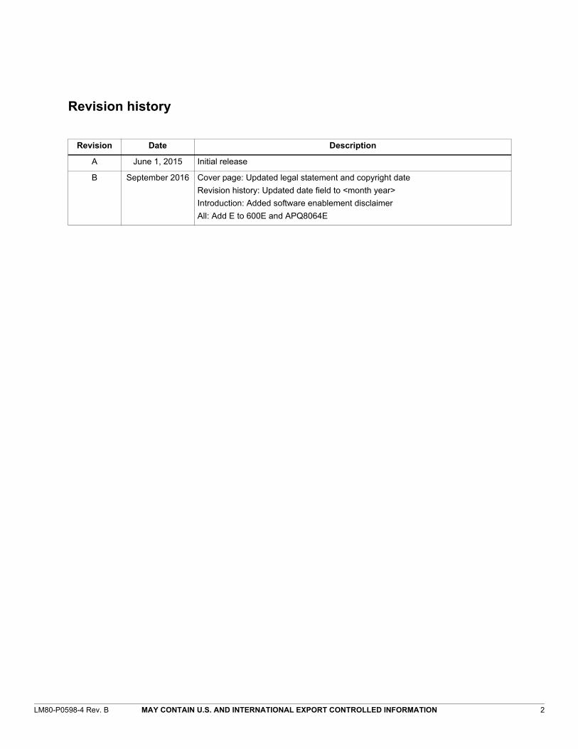
Revision history
Revision Date Description
A June 1, 2015 Initial release
B September 2016 Cover page: Updated legal statement and copyright date
Revision history: Updated date field to <month year>
Introduction: Added software enablement disclaimer
All: Add E to 600E and APQ8064E
LM80-P0598-4 Rev. B MAY CONTAIN U.S. AND INTERNATIONAL EXPORT CONTROLLED INFORMATION 3
Contents
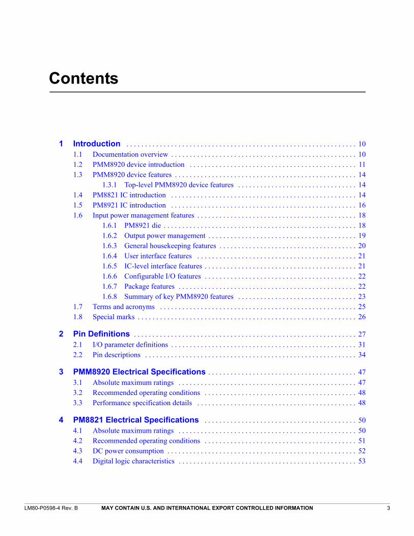
1 Introduction . . . . . . . . . . . . . . . . . . . . . . . . . . . . . . . . . . . . . . . . . . . . . . . . . . . . . . . . . . . . . . 10
1.1 Documentation overview . . . . . . . . . . . . . . . . . . . . . . . . . . . . . . . . . . . . . . . . . . . . . . . . . . 101.2 PMM8920 device introduction . . . . . . . . . . . . . . . . . . . . . . . . . . . . . . . . . . . . . . . . . . . . . 111.3 PMM8920 device features . . . . . . . . . . . . . . . . . . . . . . . . . . . . . . . . . . . . . . . . . . . . . . . . . 14
1.3.1 Top-level PMM8920 device features . . . . . . . . . . . . . . . . . . . . . . . . . . . . . . . . 141.4 PM8821 IC introduction . . . . . . . . . . . . . . . . . . . . . . . . . . . . . . . . . . . . . . . . . . . . . . . . . . 141.5 PM8921 IC introduction . . . . . . . . . . . . . . . . . . . . . . . . . . . . . . . . . . . . . . . . . . . . . . . . . . 161.6 Input power management features . . . . . . . . . . . . . . . . . . . . . . . . . . . . . . . . . . . . . . . . . . . 18
1.6.1 PM8921 die . . . . . . . . . . . . . . . . . . . . . . . . . . . . . . . . . . . . . . . . . . . . . . . . . . . . 181.6.2 Output power management . . . . . . . . . . . . . . . . . . . . . . . . . . . . . . . . . . . . . . . . 191.6.3 General housekeeping features . . . . . . . . . . . . . . . . . . . . . . . . . . . . . . . . . . . . . 201.6.4 User interface features . . . . . . . . . . . . . . . . . . . . . . . . . . . . . . . . . . . . . . . . . . . 211.6.5 IC-level interface features . . . . . . . . . . . . . . . . . . . . . . . . . . . . . . . . . . . . . . . . . 211.6.6 Configurable I/O features . . . . . . . . . . . . . . . . . . . . . . . . . . . . . . . . . . . . . . . . . 221.6.7 Package features . . . . . . . . . . . . . . . . . . . . . . . . . . . . . . . . . . . . . . . . . . . . . . . . 221.6.8 Summary of key PMM8920 features . . . . . . . . . . . . . . . . . . . . . . . . . . . . . . . . 23
1.7 Terms and acronyms . . . . . . . . . . . . . . . . . . . . . . . . . . . . . . . . . . . . . . . . . . . . . . . . . . . . . 251.8 Special marks . . . . . . . . . . . . . . . . . . . . . . . . . . . . . . . . . . . . . . . . . . . . . . . . . . . . . . . . . . . 26
2 Pin Definitions . . . . . . . . . . . . . . . . . . . . . . . . . . . . . . . . . . . . . . . . . . . . . . . . . . . . . . . . . . . . 27
2.1 I/O parameter definitions . . . . . . . . . . . . . . . . . . . . . . . . . . . . . . . . . . . . . . . . . . . . . . . . . . 312.2 Pin descriptions . . . . . . . . . . . . . . . . . . . . . . . . . . . . . . . . . . . . . . . . . . . . . . . . . . . . . . . . . 34
3 PMM8920 Electrical Specifications . . . . . . . . . . . . . . . . . . . . . . . . . . . . . . . . . . . . . . . . 47
3.1 Absolute maximum ratings . . . . . . . . . . . . . . . . . . . . . . . . . . . . . . . . . . . . . . . . . . . . . . . . 473.2 Recommended operating conditions . . . . . . . . . . . . . . . . . . . . . . . . . . . . . . . . . . . . . . . . . 483.3 Performance specification details . . . . . . . . . . . . . . . . . . . . . . . . . . . . . . . . . . . . . . . . . . . 48
4 PM8821 Electrical Specifications . . . . . . . . . . . . . . . . . . . . . . . . . . . . . . . . . . . . . . . . . 50
4.1 Absolute maximum ratings . . . . . . . . . . . . . . . . . . . . . . . . . . . . . . . . . . . . . . . . . . . . . . . . 504.2 Recommended operating conditions . . . . . . . . . . . . . . . . . . . . . . . . . . . . . . . . . . . . . . . . . 514.3 DC power consumption . . . . . . . . . . . . . . . . . . . . . . . . . . . . . . . . . . . . . . . . . . . . . . . . . . . 524.4 Digital logic characteristics . . . . . . . . . . . . . . . . . . . . . . . . . . . . . . . . . . . . . . . . . . . . . . . . 53

PMM8920 Power Management Module Device Specification Contents
LM80-P0598-4 Rev. B MAY CONTAIN U.S. AND INTERNATIONAL EXPORT CONTROLLED INFORMATION 4
4.5 Output power management . . . . . . . . . . . . . . . . . . . . . . . . . . . . . . . . . . . . . . . . . . . . . . . . 544.5.1 Reference circuit . . . . . . . . . . . . . . . . . . . . . . . . . . . . . . . . . . . . . . . . . . . . . . . . 554.5.2 Buck switched-mode power supplies . . . . . . . . . . . . . . . . . . . . . . . . . . . . . . . . 554.5.3 Linear regulators . . . . . . . . . . . . . . . . . . . . . . . . . . . . . . . . . . . . . . . . . . . . . . . . 57
4.6 General housekeeping . . . . . . . . . . . . . . . . . . . . . . . . . . . . . . . . . . . . . . . . . . . . . . . . . . . . 594.6.1 19.2 MHz clock . . . . . . . . . . . . . . . . . . . . . . . . . . . . . . . . . . . . . . . . . . . . . . . . . 594.6.2 Overtemperature protection (smart thermal control) . . . . . . . . . . . . . . . . . . . . 59
4.7 User interfaces . . . . . . . . . . . . . . . . . . . . . . . . . . . . . . . . . . . . . . . . . . . . . . . . . . . . . . . . . . 604.7.1 MPP pin specifications . . . . . . . . . . . . . . . . . . . . . . . . . . . . . . . . . . . . . . . . . . . 604.7.2 Digital control output . . . . . . . . . . . . . . . . . . . . . . . . . . . . . . . . . . . . . . . . . . . . 61
4.8 IC-level interfaces . . . . . . . . . . . . . . . . . . . . . . . . . . . . . . . . . . . . . . . . . . . . . . . . . . . . . . . 614.8.1 Poweron circuits and the power sequences . . . . . . . . . . . . . . . . . . . . . . . . . . . . 614.8.2 SSBI and the interrupt manager . . . . . . . . . . . . . . . . . . . . . . . . . . . . . . . . . . . . 61
5 PM8921 Electrical Specifications . . . . . . . . . . . . . . . . . . . . . . . . . . . . . . . . . . . . . . . . . 62
5.1 Absolute maximum ratings . . . . . . . . . . . . . . . . . . . . . . . . . . . . . . . . . . . . . . . . . . . . . . . . 625.2 Recommended operating conditions . . . . . . . . . . . . . . . . . . . . . . . . . . . . . . . . . . . . . . . . . 635.3 DC power consumption . . . . . . . . . . . . . . . . . . . . . . . . . . . . . . . . . . . . . . . . . . . . . . . . . . . 645.4 Digital logic characteristics . . . . . . . . . . . . . . . . . . . . . . . . . . . . . . . . . . . . . . . . . . . . . . . . 655.5 Input power management . . . . . . . . . . . . . . . . . . . . . . . . . . . . . . . . . . . . . . . . . . . . . . . . . . 65
5.5.1 Wall charging over-voltage protection . . . . . . . . . . . . . . . . . . . . . . . . . . . . . . . 655.5.2 External supply detection . . . . . . . . . . . . . . . . . . . . . . . . . . . . . . . . . . . . . . . . . 665.5.3 SMBC . . . . . . . . . . . . . . . . . . . . . . . . . . . . . . . . . . . . . . . . . . . . . . . . . . . . . . . . 685.5.4 Battery monitoring system . . . . . . . . . . . . . . . . . . . . . . . . . . . . . . . . . . . . . . . . 745.5.5 Coincell charging . . . . . . . . . . . . . . . . . . . . . . . . . . . . . . . . . . . . . . . . . . . . . . . 79
5.6 Output power management . . . . . . . . . . . . . . . . . . . . . . . . . . . . . . . . . . . . . . . . . . . . . . . . 805.6.1 Reference circuit . . . . . . . . . . . . . . . . . . . . . . . . . . . . . . . . . . . . . . . . . . . . . . . . 835.6.2 Buck SMPS . . . . . . . . . . . . . . . . . . . . . . . . . . . . . . . . . . . . . . . . . . . . . . . . . . . . 845.6.3 Linear regulators . . . . . . . . . . . . . . . . . . . . . . . . . . . . . . . . . . . . . . . . . . . . . . . . 915.6.4 PMOS LDO . . . . . . . . . . . . . . . . . . . . . . . . . . . . . . . . . . . . . . . . . . . . . . . . . . . . 935.6.5 NMOS LDO . . . . . . . . . . . . . . . . . . . . . . . . . . . . . . . . . . . . . . . . . . . . . . . . . . . 965.6.6 NCP . . . . . . . . . . . . . . . . . . . . . . . . . . . . . . . . . . . . . . . . . . . . . . . . . . . . . . . . . . 985.6.7 Voltage switches . . . . . . . . . . . . . . . . . . . . . . . . . . . . . . . . . . . . . . . . . . . . . . . . 995.6.8 Internal voltage-regulator connections . . . . . . . . . . . . . . . . . . . . . . . . . . . . . . 101
5.7 General housekeeping . . . . . . . . . . . . . . . . . . . . . . . . . . . . . . . . . . . . . . . . . . . . . . . . . . . 1015.7.1 Analog multiplexer and scaling circuits . . . . . . . . . . . . . . . . . . . . . . . . . . . . . 1025.7.2 HK/XO ADC circuit . . . . . . . . . . . . . . . . . . . . . . . . . . . . . . . . . . . . . . . . . . . . 1055.7.3 System clocks . . . . . . . . . . . . . . . . . . . . . . . . . . . . . . . . . . . . . . . . . . . . . . . . . 1085.7.4 Realtime clock . . . . . . . . . . . . . . . . . . . . . . . . . . . . . . . . . . . . . . . . . . . . . . . . . 1135.7.5 Overtemperature protection (smart thermal control) . . . . . . . . . . . . . . . . . . . 114
PMM8920 Power Management Module Device Specification Contents
LM80-P0598-4 Rev. B MAY CONTAIN U.S. AND INTERNATIONAL EXPORT CONTROLLED INFORMATION 5
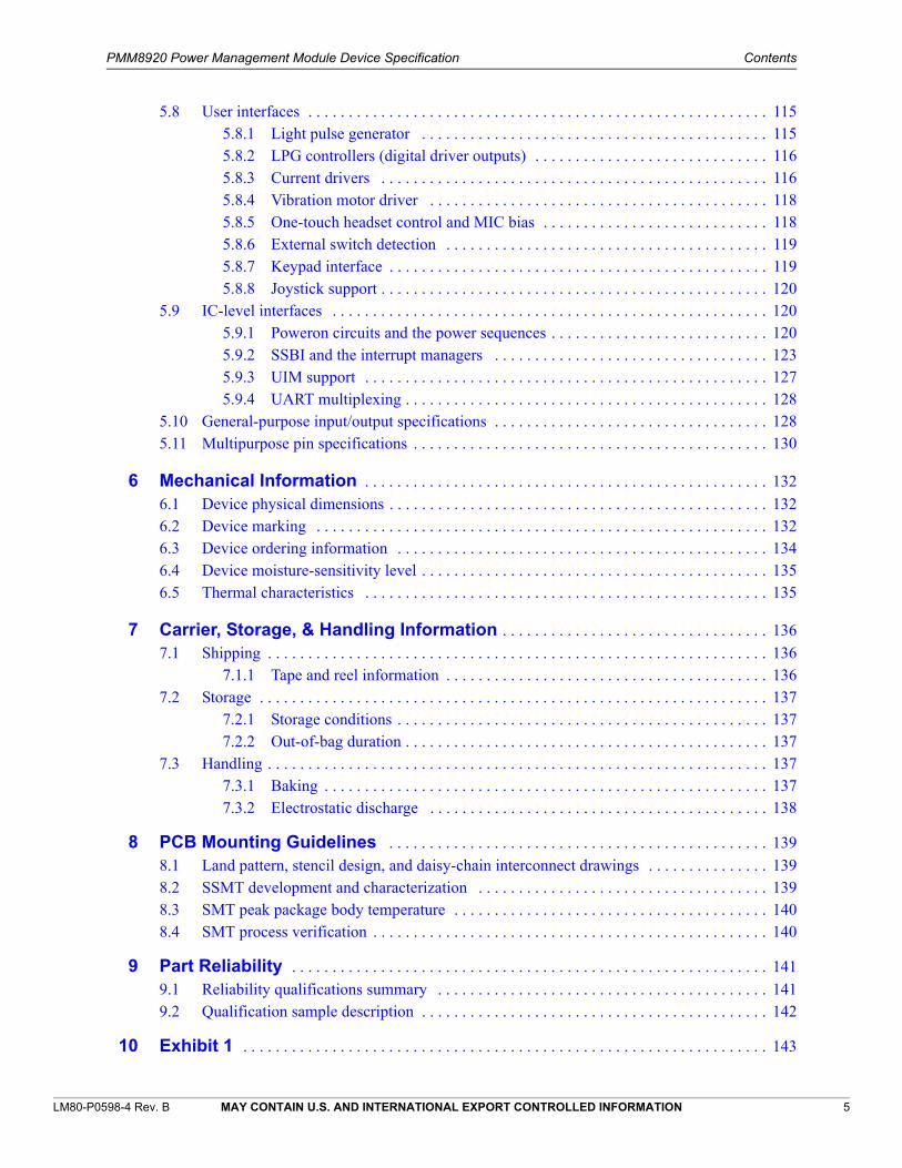
5.8 User interfaces . . . . . . . . . . . . . . . . . . . . . . . . . . . . . . . . . . . . . . . . . . . . . . . . . . . . . . . . . 1155.8.1 Light pulse generator . . . . . . . . . . . . . . . . . . . . . . . . . . . . . . . . . . . . . . . . . . . 1155.8.2 LPG controllers (digital driver outputs) . . . . . . . . . . . . . . . . . . . . . . . . . . . . . 1165.8.3 Current drivers . . . . . . . . . . . . . . . . . . . . . . . . . . . . . . . . . . . . . . . . . . . . . . . . 1165.8.4 Vibration motor driver . . . . . . . . . . . . . . . . . . . . . . . . . . . . . . . . . . . . . . . . . . 1185.8.5 One-touch headset control and MIC bias . . . . . . . . . . . . . . . . . . . . . . . . . . . . 1185.8.6 External switch detection . . . . . . . . . . . . . . . . . . . . . . . . . . . . . . . . . . . . . . . . 1195.8.7 Keypad interface . . . . . . . . . . . . . . . . . . . . . . . . . . . . . . . . . . . . . . . . . . . . . . . 1195.8.8 Joystick support . . . . . . . . . . . . . . . . . . . . . . . . . . . . . . . . . . . . . . . . . . . . . . . . 120
5.9 IC-level interfaces . . . . . . . . . . . . . . . . . . . . . . . . . . . . . . . . . . . . . . . . . . . . . . . . . . . . . . 1205.9.1 Poweron circuits and the power sequences . . . . . . . . . . . . . . . . . . . . . . . . . . . 1205.9.2 SSBI and the interrupt managers . . . . . . . . . . . . . . . . . . . . . . . . . . . . . . . . . . 1235.9.3 UIM support . . . . . . . . . . . . . . . . . . . . . . . . . . . . . . . . . . . . . . . . . . . . . . . . . . 1275.9.4 UART multiplexing . . . . . . . . . . . . . . . . . . . . . . . . . . . . . . . . . . . . . . . . . . . . . 128
5.10 General-purpose input/output specifications . . . . . . . . . . . . . . . . . . . . . . . . . . . . . . . . . . 1285.11 Multipurpose pin specifications . . . . . . . . . . . . . . . . . . . . . . . . . . . . . . . . . . . . . . . . . . . . 130
6 Mechanical Information . . . . . . . . . . . . . . . . . . . . . . . . . . . . . . . . . . . . . . . . . . . . . . . . . . 132
6.1 Device physical dimensions . . . . . . . . . . . . . . . . . . . . . . . . . . . . . . . . . . . . . . . . . . . . . . . 1326.2 Device marking . . . . . . . . . . . . . . . . . . . . . . . . . . . . . . . . . . . . . . . . . . . . . . . . . . . . . . . . 1326.3 Device ordering information . . . . . . . . . . . . . . . . . . . . . . . . . . . . . . . . . . . . . . . . . . . . . . 1346.4 Device moisture-sensitivity level . . . . . . . . . . . . . . . . . . . . . . . . . . . . . . . . . . . . . . . . . . . 1356.5 Thermal characteristics . . . . . . . . . . . . . . . . . . . . . . . . . . . . . . . . . . . . . . . . . . . . . . . . . . 135
7 Carrier, Storage, & Handling Information . . . . . . . . . . . . . . . . . . . . . . . . . . . . . . . . . 136
7.1 Shipping . . . . . . . . . . . . . . . . . . . . . . . . . . . . . . . . . . . . . . . . . . . . . . . . . . . . . . . . . . . . . . 1367.1.1 Tape and reel information . . . . . . . . . . . . . . . . . . . . . . . . . . . . . . . . . . . . . . . . 136
7.2 Storage . . . . . . . . . . . . . . . . . . . . . . . . . . . . . . . . . . . . . . . . . . . . . . . . . . . . . . . . . . . . . . . 1377.2.1 Storage conditions . . . . . . . . . . . . . . . . . . . . . . . . . . . . . . . . . . . . . . . . . . . . . . 1377.2.2 Out-of-bag duration . . . . . . . . . . . . . . . . . . . . . . . . . . . . . . . . . . . . . . . . . . . . . 137
7.3 Handling . . . . . . . . . . . . . . . . . . . . . . . . . . . . . . . . . . . . . . . . . . . . . . . . . . . . . . . . . . . . . . 1377.3.1 Baking . . . . . . . . . . . . . . . . . . . . . . . . . . . . . . . . . . . . . . . . . . . . . . . . . . . . . . . 1377.3.2 Electrostatic discharge . . . . . . . . . . . . . . . . . . . . . . . . . . . . . . . . . . . . . . . . . . 138
8 PCB Mounting Guidelines . . . . . . . . . . . . . . . . . . . . . . . . . . . . . . . . . . . . . . . . . . . . . . . 139
8.1 Land pattern, stencil design, and daisy-chain interconnect drawings . . . . . . . . . . . . . . . 1398.2 SSMT development and characterization . . . . . . . . . . . . . . . . . . . . . . . . . . . . . . . . . . . . 1398.3 SMT peak package body temperature . . . . . . . . . . . . . . . . . . . . . . . . . . . . . . . . . . . . . . . 1408.4 SMT process verification . . . . . . . . . . . . . . . . . . . . . . . . . . . . . . . . . . . . . . . . . . . . . . . . . 140
9 Part Reliability . . . . . . . . . . . . . . . . . . . . . . . . . . . . . . . . . . . . . . . . . . . . . . . . . . . . . . . . . . . 141
9.1 Reliability qualifications summary . . . . . . . . . . . . . . . . . . . . . . . . . . . . . . . . . . . . . . . . . 1419.2 Qualification sample description . . . . . . . . . . . . . . . . . . . . . . . . . . . . . . . . . . . . . . . . . . . 142
10 Exhibit 1 . . . . . . . . . . . . . . . . . . . . . . . . . . . . . . . . . . . . . . . . . . . . . . . . . . . . . . . . . . . . . . . . . 143

PMM8920 Power Management Module Device Specification Contents
LM80-P0598-4 Rev. B MAY CONTAIN U.S. AND INTERNATIONAL EXPORT CONTROLLED INFORMATION 6
Figures
Figure 1-1 High-level PMM8920 functional block diagram . . . . . . . . . . . . . . . . . . . . . . . . . . . . 13Figure 1-2 High-level PM8821 IC functional block diagram . . . . . . . . . . . . . . . . . . . . . . . . . . . 15Figure 1-3 High-level PM8921 IC functional block diagram . . . . . . . . . . . . . . . . . . . . . . . . . . . 17Figure 2-1 PMM8920 module pin assignments (top view) . . . . . . . . . . . . . . . . . . . . . . . . . . . . . 28Figure 2-2 Pin assignments – left half . . . . . . . . . . . . . . . . . . . . . . . . . . . . . . . . . . . . . . . . . . . . . 29Figure 2-3 Pin assignments – right half . . . . . . . . . . . . . . . . . . . . . . . . . . . . . . . . . . . . . . . . . . . . 30Figure 4-1 FT SMPS efficiency . . . . . . . . . . . . . . . . . . . . . . . . . . . . . . . . . . . . . . . . . . . . . . . . . . 57Figure 5-1 Charging flow diagram . . . . . . . . . . . . . . . . . . . . . . . . . . . . . . . . . . . . . . . . . . . . . . . 71Figure 5-2 BTM diagram . . . . . . . . . . . . . . . . . . . . . . . . . . . . . . . . . . . . . . . . . . . . . . . . . . . . . . . 78Figure 5-3 S1 PWM mode . . . . . . . . . . . . . . . . . . . . . . . . . . . . . . . . . . . . . . . . . . . . . . . . . . . . . . 87Figure 5-4 S2 PWM mode . . . . . . . . . . . . . . . . . . . . . . . . . . . . . . . . . . . . . . . . . . . . . . . . . . . . . . 87Figure 5-5 S3 PWM mode . . . . . . . . . . . . . . . . . . . . . . . . . . . . . . . . . . . . . . . . . . . . . . . . . . . . . . 88Figure 5-6 S4 PWM mode . . . . . . . . . . . . . . . . . . . . . . . . . . . . . . . . . . . . . . . . . . . . . . . . . . . . . . 88Figure 5-7 S5 - FT SMPS . . . . . . . . . . . . . . . . . . . . . . . . . . . . . . . . . . . . . . . . . . . . . . . . . . . . . . 89Figure 5-8 S6 - FT SMPS . . . . . . . . . . . . . . . . . . . . . . . . . . . . . . . . . . . . . . . . . . . . . . . . . . . . . . 89Figure 5-9 S7 PWM mode . . . . . . . . . . . . . . . . . . . . . . . . . . . . . . . . . . . . . . . . . . . . . . . . . . . . . . 90Figure 5-10 S8 PWM mode . . . . . . . . . . . . . . . . . . . . . . . . . . . . . . . . . . . . . . . . . . . . . . . . . . . . . 90Figure 5-11 Multiplexer offset and gain errors . . . . . . . . . . . . . . . . . . . . . . . . . . . . . . . . . . . . . 104Figure 5-12 Analog multiplexer load condition for settling time specification . . . . . . . . . . . . 104Figure 5-13 KPD_DRV chart . . . . . . . . . . . . . . . . . . . . . . . . . . . . . . . . . . . . . . . . . . . . . . . . . . 117Figure 5-14 Example high-level power sequence timing diagram for PM8921 IC when paired with APQ8064E IC (OPT1 = VDD, OPT2 = Hi-Z, OPT3 = VDD) . . . . . . . . . . . . . . . . . . . . . 122Figure 6-1 PMM8920 device marking (top view – not to scale) . . . . . . . . . . . . . . . . . . . . . . . . 132Figure 6-2 Device identification code . . . . . . . . . . . . . . . . . . . . . . . . . . . . . . . . . . . . . . . . . . . . 134Figure 7-1 Carrier tape drawing with part orientation . . . . . . . . . . . . . . . . . . . . . . . . . . . . . . . . 136Figure 7-2 Tape handling . . . . . . . . . . . . . . . . . . . . . . . . . . . . . . . . . . . . . . . . . . . . . . . . . . . . . 137
PMM8920 Power Management Module Device Specification Contents
LM80-P0598-4 Rev. B MAY CONTAIN U.S. AND INTERNATIONAL EXPORT CONTROLLED INFORMATION 7
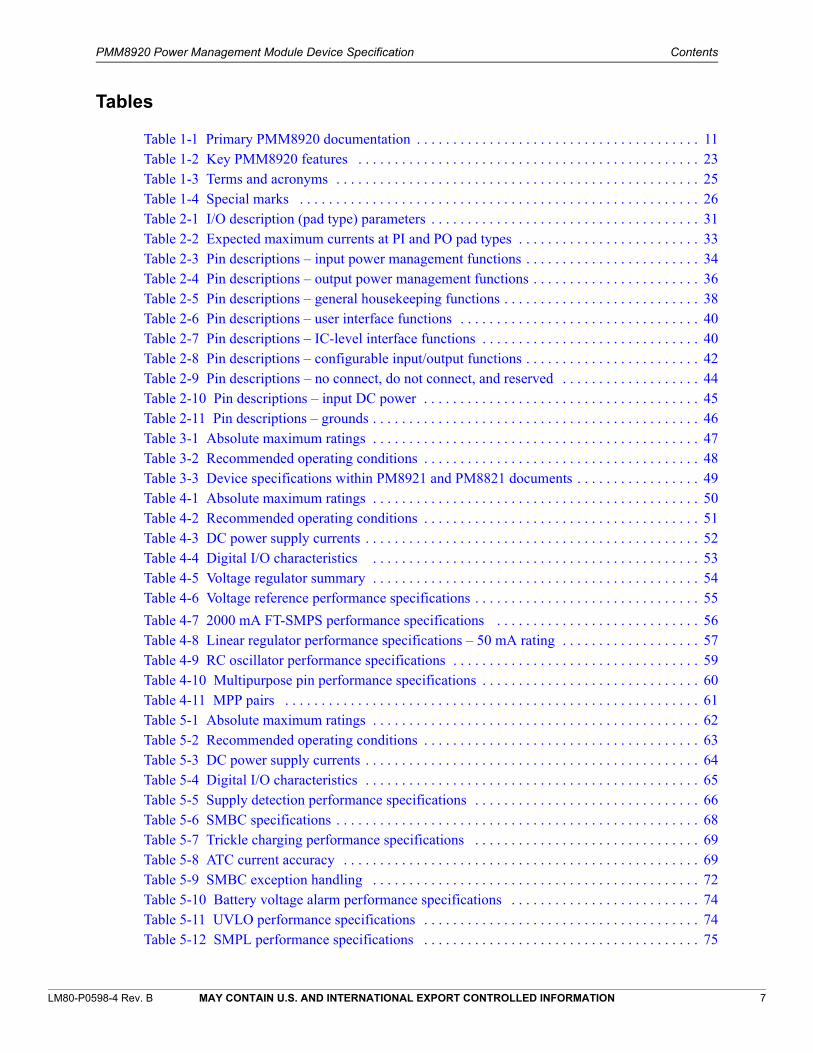
Tables
Table 1-1 Primary PMM8920 documentation . . . . . . . . . . . . . . . . . . . . . . . . . . . . . . . . . . . . . . . 11Table 1-2 Key PMM8920 features . . . . . . . . . . . . . . . . . . . . . . . . . . . . . . . . . . . . . . . . . . . . . . . 23Table 1-3 Terms and acronyms . . . . . . . . . . . . . . . . . . . . . . . . . . . . . . . . . . . . . . . . . . . . . . . . . . 25Table 1-4 Special marks . . . . . . . . . . . . . . . . . . . . . . . . . . . . . . . . . . . . . . . . . . . . . . . . . . . . . . . 26Table 2-1 I/O description (pad type) parameters . . . . . . . . . . . . . . . . . . . . . . . . . . . . . . . . . . . . . 31Table 2-2 Expected maximum currents at PI and PO pad types . . . . . . . . . . . . . . . . . . . . . . . . . 33Table 2-3 Pin descriptions – input power management functions . . . . . . . . . . . . . . . . . . . . . . . . 34Table 2-4 Pin descriptions – output power management functions . . . . . . . . . . . . . . . . . . . . . . . 36Table 2-5 Pin descriptions – general housekeeping functions . . . . . . . . . . . . . . . . . . . . . . . . . . . 38Table 2-6 Pin descriptions – user interface functions . . . . . . . . . . . . . . . . . . . . . . . . . . . . . . . . . 40Table 2-7 Pin descriptions – IC-level interface functions . . . . . . . . . . . . . . . . . . . . . . . . . . . . . . 40Table 2-8 Pin descriptions – configurable input/output functions . . . . . . . . . . . . . . . . . . . . . . . . 42Table 2-9 Pin descriptions – no connect, do not connect, and reserved . . . . . . . . . . . . . . . . . . . 44Table 2-10 Pin descriptions – input DC power . . . . . . . . . . . . . . . . . . . . . . . . . . . . . . . . . . . . . . 45Table 2-11 Pin descriptions – grounds . . . . . . . . . . . . . . . . . . . . . . . . . . . . . . . . . . . . . . . . . . . . . 46Table 3-1 Absolute maximum ratings . . . . . . . . . . . . . . . . . . . . . . . . . . . . . . . . . . . . . . . . . . . . . 47Table 3-2 Recommended operating conditions . . . . . . . . . . . . . . . . . . . . . . . . . . . . . . . . . . . . . . 48Table 3-3 Device specifications within PM8921 and PM8821 documents . . . . . . . . . . . . . . . . . 49Table 4-1 Absolute maximum ratings . . . . . . . . . . . . . . . . . . . . . . . . . . . . . . . . . . . . . . . . . . . . . 50Table 4-2 Recommended operating conditions . . . . . . . . . . . . . . . . . . . . . . . . . . . . . . . . . . . . . . 51Table 4-3 DC power supply currents . . . . . . . . . . . . . . . . . . . . . . . . . . . . . . . . . . . . . . . . . . . . . . 52Table 4-4 Digital I/O characteristics . . . . . . . . . . . . . . . . . . . . . . . . . . . . . . . . . . . . . . . . . . . . . 53Table 4-5 Voltage regulator summary . . . . . . . . . . . . . . . . . . . . . . . . . . . . . . . . . . . . . . . . . . . . . 54Table 4-6 Voltage reference performance specifications . . . . . . . . . . . . . . . . . . . . . . . . . . . . . . . 55
Table 4-7 2000 mA FT-SMPS performance specifications . . . . . . . . . . . . . . . . . . . . . . . . . . . . 56Table 4-8 Linear regulator performance specifications – 50 mA rating . . . . . . . . . . . . . . . . . . . 57Table 4-9 RC oscillator performance specifications . . . . . . . . . . . . . . . . . . . . . . . . . . . . . . . . . . 59Table 4-10 Multipurpose pin performance specifications . . . . . . . . . . . . . . . . . . . . . . . . . . . . . . 60Table 4-11 MPP pairs . . . . . . . . . . . . . . . . . . . . . . . . . . . . . . . . . . . . . . . . . . . . . . . . . . . . . . . . . 61Table 5-1 Absolute maximum ratings . . . . . . . . . . . . . . . . . . . . . . . . . . . . . . . . . . . . . . . . . . . . . 62Table 5-2 Recommended operating conditions . . . . . . . . . . . . . . . . . . . . . . . . . . . . . . . . . . . . . . 63Table 5-3 DC power supply currents . . . . . . . . . . . . . . . . . . . . . . . . . . . . . . . . . . . . . . . . . . . . . . 64Table 5-4 Digital I/O characteristics . . . . . . . . . . . . . . . . . . . . . . . . . . . . . . . . . . . . . . . . . . . . . . 65Table 5-5 Supply detection performance specifications . . . . . . . . . . . . . . . . . . . . . . . . . . . . . . . 66Table 5-6 SMBC specifications . . . . . . . . . . . . . . . . . . . . . . . . . . . . . . . . . . . . . . . . . . . . . . . . . . 68Table 5-7 Trickle charging performance specifications . . . . . . . . . . . . . . . . . . . . . . . . . . . . . . . 69Table 5-8 ATC current accuracy . . . . . . . . . . . . . . . . . . . . . . . . . . . . . . . . . . . . . . . . . . . . . . . . . 69Table 5-9 SMBC exception handling . . . . . . . . . . . . . . . . . . . . . . . . . . . . . . . . . . . . . . . . . . . . . 72Table 5-10 Battery voltage alarm performance specifications . . . . . . . . . . . . . . . . . . . . . . . . . . 74Table 5-11 UVLO performance specifications . . . . . . . . . . . . . . . . . . . . . . . . . . . . . . . . . . . . . . 74Table 5-12 SMPL performance specifications . . . . . . . . . . . . . . . . . . . . . . . . . . . . . . . . . . . . . . 75

PMM8920 Power Management Module Device Specification Contents
LM80-P0598-4 Rev. B MAY CONTAIN U.S. AND INTERNATIONAL EXPORT CONTROLLED INFORMATION 8
Table 5-13 External battery P-channel MOSFET specifications . . . . . . . . . . . . . . . . . . . . . . . . . 75Table 5-14 External MOSFET driver specifications . . . . . . . . . . . . . . . . . . . . . . . . . . . . . . . . . . 76Table 5-15 Battery fuel gauge specifications . . . . . . . . . . . . . . . . . . . . . . . . . . . . . . . . . . . . . . . 76Table 5-16 Sensed current accuracy . . . . . . . . . . . . . . . . . . . . . . . . . . . . . . . . . . . . . . . . . . . . . . 76Table 5-17 VDD collapse protection performance specifications . . . . . . . . . . . . . . . . . . . . . . . . 77Table 5-18 Battery interface specifications . . . . . . . . . . . . . . . . . . . . . . . . . . . . . . . . . . . . . . . . . 77Table 5-19 BTM calculations . . . . . . . . . . . . . . . . . . . . . . . . . . . . . . . . . . . . . . . . . . . . . . . . . . . 79Table 5-20 Coincell charging performance specifications . . . . . . . . . . . . . . . . . . . . . . . . . . . . . 79Table 5-21 Output power management summary . . . . . . . . . . . . . . . . . . . . . . . . . . . . . . . . . . . . 80Table 5-22 Voltage reference performance specifications . . . . . . . . . . . . . . . . . . . . . . . . . . . . . . 83Table 5-23 HF-SMPS performance specifications . . . . . . . . . . . . . . . . . . . . . . . . . . . . . . . . . . . 84Table 5-24 2000 mA FT-SMPS performance specifications . . . . . . . . . . . . . . . . . . . . . . . . . . . . 86Table 5-25 Linear regulator performance specifications – 1200 mA rating . . . . . . . . . . . . . . . . 91Table 5-26 LDO regulator specifications . . . . . . . . . . . . . . . . . . . . . . . . . . . . . . . . . . . . . . . . . . 93Table 5-27 LDO regulator typical specifications . . . . . . . . . . . . . . . . . . . . . . . . . . . . . . . . . . . . 95Table 5-28 LDO regulator specifications for VREG_XO and VREG_RFCLK . . . . . . . . . . . . . 95Table 5-29 Linear regulator performance specifications – 150 mA rating . . . . . . . . . . . . . . . . . 96Table 5-30 LDO regulator typical specifications . . . . . . . . . . . . . . . . . . . . . . . . . . . . . . . . . . . . 97Table 5-31 NCP regulator performance specifications . . . . . . . . . . . . . . . . . . . . . . . . . . . . . . . . 98Table 5-32 100 mA low-voltage switch specifications . . . . . . . . . . . . . . . . . . . . . . . . . . . . . . . . 99Table 5-33 300 mA low-voltage switch specifications . . . . . . . . . . . . . . . . . . . . . . . . . . . . . . . . 99Table 5-34 65 mA MVS (HDMI) switch specifications . . . . . . . . . . . . . . . . . . . . . . . . . . . . . . 100Table 5-35 500 mA MVS (OTG) switch specifications . . . . . . . . . . . . . . . . . . . . . . . . . . . . . . 100Table 5-36 Internal voltage-regulator connections . . . . . . . . . . . . . . . . . . . . . . . . . . . . . . . . . . 101Table 5-37 Analog multiplexer and scaling functions . . . . . . . . . . . . . . . . . . . . . . . . . . . . . . . . 102Table 5-38 Analog multiplexer performance specifications . . . . . . . . . . . . . . . . . . . . . . . . . . . 103Table 5-39 HK/XO ADC performance specifications . . . . . . . . . . . . . . . . . . . . . . . . . . . . . . . . 105Table 5-40 AMUX input to ADC output end-to-end accuracy specifications . . . . . . . . . . . . . 106Table 5-41 Specifications for XO_OUT_D0 and XO_OUT_D1 . . . . . . . . . . . . . . . . . . . . . . . 109Table 5-42 Typical 19.2 MHz crystal specifications (2520 size) . . . . . . . . . . . . . . . . . . . . . . . 110Table 5-43 Specifications for XO_OUT_A0, XO_OUT_A1, and XO_OUT_A2 . . . . . . . . . . 111Table 5-44 Typical 32 kHz crystal specification . . . . . . . . . . . . . . . . . . . . . . . . . . . . . . . . . . . . 112Table 5-45 RC oscillator performance specifications . . . . . . . . . . . . . . . . . . . . . . . . . . . . . . . . 113Table 5-46 RTC performance specs when using Cal RC, XO/586 and 32 kHz oscillator . . . . 114Table 5-47 Current driver performance specifications . . . . . . . . . . . . . . . . . . . . . . . . . . . . . . . 116Table 5-48 Vibration motor driver performance specifications . . . . . . . . . . . . . . . . . . . . . . . . . 118Table 5-49 HSED and MIC bias performance specifications . . . . . . . . . . . . . . . . . . . . . . . . . . 119Table 5-50 Keypad interface performance specifications . . . . . . . . . . . . . . . . . . . . . . . . . . . . . 119Table 5-51 Poweron circuit performance specifications . . . . . . . . . . . . . . . . . . . . . . . . . . . . . . 121Table 5-52 PM8921 interrupt list . . . . . . . . . . . . . . . . . . . . . . . . . . . . . . . . . . . . . . . . . . . . . . . . 123Table 5-53 UIM signal paths . . . . . . . . . . . . . . . . . . . . . . . . . . . . . . . . . . . . . . . . . . . . . . . . . . . 127Table 5-54 PM8921 UART functions . . . . . . . . . . . . . . . . . . . . . . . . . . . . . . . . . . . . . . . . . . . . 128Table 5-55 Programmable GPIO configurations . . . . . . . . . . . . . . . . . . . . . . . . . . . . . . . . . . . . 128
PMM8920 Power Management Module Device Specification Contents
LM80-P0598-4 Rev. B MAY CONTAIN U.S. AND INTERNATIONAL EXPORT CONTROLLED INFORMATION 9
Table 5-56 Special GPIO default states . . . . . . . . . . . . . . . . . . . . . . . . . . . . . . . . . . . . . . . . . . . 129Table 5-57 VOL and VOH for different driver strengths . . . . . . . . . . . . . . . . . . . . . . . . . . . . . 129Table 5-58 Multipurpose pin performance specifications . . . . . . . . . . . . . . . . . . . . . . . . . . . . . 130Table 5-59 MPP pairs . . . . . . . . . . . . . . . . . . . . . . . . . . . . . . . . . . . . . . . . . . . . . . . . . . . . . . . . 131Table 6-1 Part marking line descriptions . . . . . . . . . . . . . . . . . . . . . . . . . . . . . . . . . . . . . . . . . . 132Table 6-2 Device identification code/ordering information details . . . . . . . . . . . . . . . . . . . . . . 134Table 6-3 Device thermal resistance . . . . . . . . . . . . . . . . . . . . . . . . . . . . . . . . . . . . . . . . . . . . . 135Table 8-1 Typical SMT reflow profile conditions (for reference only) . . . . . . . . . . . . . . . . . . . 140Table 9-1 PMM8160 IC reliability evaluation . . . . . . . . . . . . . . . . . . . . . . . . . . . . . . . . . . . . . 141
LM80-P0598-4 Rev. B MAY CONTAIN U.S. AND INTERNATIONAL EXPORT CONTROLLED INFORMATION 10
1 Introduction
This document describes the features and functionality of the PMM8920 Power Management Module on Qualcomm® Snapdragon™ 600E (APQ8064E) processor. Qualcomm processors for embedded computing are dedicated to support embedded device OEMs in several ways:
Longevity beyond lifecycle of mobile chipsets through 2020
Detailed documentation for developers
Availability of development kits/community board for early access
Multiple OS support including mainline Linux support
Availability of several computing module partners for customization for your individualprojects and products
Snapdragon 600E processors deliver high-performance computing, low-power consumption, and a rich multimedia experience for embedded devices.
It is an ideal solution for any application that requires computing horsepower and integrated Wi-Fi/Bluetooth connectivity, such as:
Smart Home
Industrial Appliances
Digital Media and TV dongles
Smart Surveillance
Robotics
Snapdragon supports a clear deployment path for embedded device OEMs and developers – starting with single-board computers and development kits, and scaling up to customer solutions, integration services, and production-ready, customizable computing modules.
This document provides a description of chipset capabilities. Not all features are available, nor are all features supported in the software.
NOTE Enabling some features may require additional licensing fees.
1.1 Documentation overview
Technical information for the PMM8920 power management module is primarily covered by the documents listed in Table 1-1. Each is a self-contained document, but a thorough understanding of the device and its applications requires familiarization with all of them. The device description in Section 1.2 is a good place to start.
PMM8920 Power Management Module Device Specification Introduction
LM80-P0598-4 Rev. B MAY CONTAIN U.S. AND INTERNATIONAL EXPORT CONTROLLED INFORMATION 11
This PMM8920 device specification is organized as follows:
Chapter 1 Provides an overview of the PMM8920 documentation, gives a high-level functional block diagram of the device, lists the device features, and defines marking conventions, terms, and acronyms used throughout this document.
Chapter 2 Defines the device pin assignments.
Chapter 3 Defines PMM8920 absolute maximum ratings and recommended operating conditions.
Chapter 4 Defines PM8821 electrical performance.
Chapter 5 Defines PM8921 electrical performance.
Chapter 6 Provides module mechanical information, including dimensions, markings, ordering information, moisture sensitivity, and thermal characteristics.
Chapter 7 Discusses shipping, storage, and handling of PMM8920 devices.
Chapter 8 Presents procedures and specifications for mounting the PMM8920 device onto PCBs.
Chapter 9 Presents PMM8920 device reliability data, including a definition of the qualification samples and a summary of qualification test results.
Chapter 10 Provides the details of the licensing agreement.
1.2 PMM8920 device introduction
The PMM8920 device is a module that integrates two power management die (PM8921 and PM8821 die) into a single package. Like the individual PMICs, the PMM8920 device functionality (Figure 1-1) is partitioned into five major blocks to simplify discussion:
Input power management
Output power management
General housekeeping
Table 1-1 Primary PMM8920 documentation
Title Description
PMM8920 Power Management Module Device Specification
(this document)
Introduces the PMM8920 device that integrates two power management (PM) die (PM8921 and PM8821 die) into a single module, and then defines: its pin assignments; composite (PM8921 + PM8821 IC) electrical specifications; mechanical packaging; shipping, storage, and handling instructions; printed circuit board (PCB) mounting guidelines; and part reliability. This document can be used by company purchasing departments to facilitate procurement.
Qualcomm Snapdragon 600E Processor
(APQ8064E) Chipset Data Sheet
Detailed functional and interface descriptions for all chipset ICs:
RF transceiver; WGR7640 IC for GPS
Power management: PMM8920 IC
WLAN and FM radio: QCA6234 IC
Audio codec: WCD9311 IC

PMM8920 Power Management Module Device Specification Introduction
LM80-P0598-4 Rev. B MAY CONTAIN U.S. AND INTERNATIONAL EXPORT CONTROLLED INFORMATION 12
User interfaces
IC interfaces
Most of the information contained in this device specification is organized accordingly – including the circuit groupings within the block diagram (Figure 1-1), pin descriptions (Chapter 2), and detailed electrical specifications (Chapter 3).
The module also has several pins that can be configured to support the five major blocks – general-purpose input/output (GPIO) pins and multipurpose pins (MPPs). The two mixed-signal BiCMOS die are integrated into a 255-pin nano-scale package (255 FBGA) that includes several ground pins for electrical ground and thermal relief.

PMM8920 Power Management Module Device Specification Introduction
LM80-P0598-4 Rev. B MAY CONTAIN U.S. AND INTERNATIONAL EXPORT CONTROLLED INFORMATION 13
Figure 1-1 High-level PMM8920 functional block diagram
PMM8920 module
= PM8821 die
= PM8921 dieOver-voltageprotection 1
USBconn
BatteryMOSFET
VPH
_PW
R
Vib motordriver
User Interfaces
JoystickI/F
Currentdrivers
LPGdrivers
Joystick
coincell
Vibrationmotor
Input PowerManagement
to USBPHY
OVPFETs
DC_IN
Over-voltageprotection 2DC
jack
BatteryModule
source 1
source 2
Generalhousekeeping
19.2 MRCO
VREF_OUT
VREF
from IPM circuits
SMPL
other internal nodes
HK/XO ADC& controllerM
UX
Sleep clockoutputs
MP3_CLK
XOs
32 KXO
SMPSclocks
XO_THERM
AMUX &scaling
Switchesanalog inputsto MPPs
19.2 MXO
19.2 MRCO
Buffers/controls
SinewaveXO outputs
SquarewaveXO outputs
Enables
DIV
DIV
Die temp
SMPSclocks
SSBI_CLK
Internalclocks
32kRCO
VREF FT-SMPS
(x2)LC
networks
RegulatedV_OUTs (2)
Linear LDOs(x20)
Caps
RegulatedV_OUTs (20)
VREF
FT-SMPSS1, S2
LCnetworks
RegulatedV_OUTsLinear regs
L1
V switches
LVS (x7)MVS (x2)
switched LV_OUTs (7)
HF-SMPS(x5)
LCnetworks
RegulatedV_OUTs (5)
Output PowerManagement
IC interfaces
Serial bus
Lvl shift, detect,& A-mux inputs
UIM levelshifters
modem IC-side
UART = 3:1
analog inputs
SSBI_8921
Interrupts_8921
Poweroncircuits PON_RST_N_8921
PS_HOLDCBL_PWR
other inputs
Identitymodule
digital inputs
P-on
RESIN_N
Poweroncircuits
Serial bus
PM_INT_N_8821
SSBI_8821
PON_RST_N_8821
OPT control
ALT_SSBI_CLK
LV inputs (7)
switched MV_OUTs (2)MV inputs (2)
VIN_5VSVREG_S4VREG_S4
UARTMUX
UIM det
Interruptmanager
Interruptmanager
Vcoincharger Ba
ttery
mon
itorin
gsy
stem
(BM
S)–
incl
udes
fuel
gaug
e Vbat
Switc
hed-
mod
eba
ttery
char
ger
Vdd
Vchg
On PM8821 & PM8921 die: 3 MPPs, 27 GPIOs & 12 MPPsOff-die: 32 kHz crystal, VREF bypass caps, some input
bypass caps, some regulator load caps

PMM8920 Power Management Module Device Specification Introduction
LM80-P0598-4 Rev. B MAY CONTAIN U.S. AND INTERNATIONAL EXPORT CONTROLLED INFORMATION 14
1.3 PMM8920 device features
1.3.1 Top-level PMM8920 device features
Integrates two power management die into a single package (13.9 × 12.3 × 1.29 mm)
PM8921 IC (7.8 × 7.8 × 1.0 mm)
PM8821 IC (2.8 × 2.4 × 0.55 mm)
Integrates some discrete components
Reduces board area
Simplifies board layout with in-package interconnections
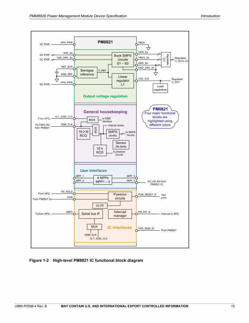
1.4 PM8821 IC introduction
The PM8821 IC is a companion device that supplements a primary PM8921 IC.
The PM8821 IC extends the PM8921 power management capabilities:
Two fast-transient switched mode power supply (FT-SMPS) circuits for powering high-performance application processor cores that exhibit highly dynamic load changes
One internal use low-dropout (LDO) linear regulator
Four configurable multipurpose pins (MPPs) for expanding the digital and analog I/O connections
The PM8821 functionality (Figure 1-1) is partitioned into four major blocks to simplify discussion:
Output voltage regulation
General housekeeping
User interfaces
IC interfaces
Most of the information contained in this device specification is organized accordingly – including the circuit groupings within the block diagram (Figure 1-2) and detailed electrical specifications (Chapter 4).
This mixed-signal BiCMOS device is available in the 42-pin wafer-level nanoscale package (42 WLNSP) that includes several ground pins for electrical ground and thermal relief.
PMM8920 Power Management Module Device Specification Introduction
LM80-P0598-4 Rev. B MAY CONTAIN U.S. AND INTERNATIONAL EXPORT CONTROLLED INFORMATION 15
Figure 1-2 High-level PM8821 IC functional block diagram
PM8821Four major functional
blocks are highlighted using different colors
PM8821
Output voltage regulation
Bandgap reference
V_REF
Buck SMPScircuitsS1 – S2
LCne
twor
ks
Regulated V_OUTs (2)
Linear regulator
L1 Loadcapacitors
Regulated V_OUT
General housekeeping
19.2 M RCO
to SMPS circuits
IC interfaces
Serial bus IF Interrupt manager
4 MPPs MPP1 – 4
19.2 MHz XO from PM8921
Interrupt to APQ
Poweroncircuits
PON_RESET_NPS_HOLD
Internal clocks
PON
SMPSclocks
Sensordie temp
User interfaces
To/from APQ
REF_BYP
VSW_Sx
VREG_Sx
VDD_DIG
SSBI_CLK
SBDT PM_INT_N
Test point
VDD_Sx
VPH_PWR
GND_REF
GND_Sx
VDD_DRV_Sx
VDD_MSM_IO
From APQ
From PM8921 IC
GNDsVPH_PWRDC PWR
DC PWR
DC PWR
DC PWR
From PM8921
ALT_SSBI_CLK
GND_DRV_Sx
MUX
MPP_1
MPP_2
MPP_3
MPP_4
ULVO
XO_D0_EN from PM8921 IC
SSBI_CLK
ALT_SSBI_CLK
MU
X
From APQ MUX to SSBI interface
32 k RCO to poweron
circuits
PMM8920 Power Management Module Device Specification Introduction
LM80-P0598-4 Rev. B MAY CONTAIN U.S. AND INTERNATIONAL EXPORT CONTROLLED INFORMATION 16
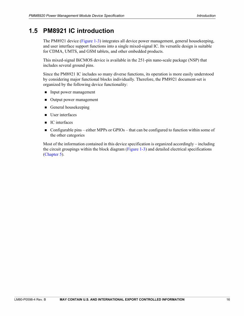
1.5 PM8921 IC introduction
The PM8921 device (Figure 1-3) integrates all device power management, general housekeeping, and user interface support functions into a single mixed-signal IC. Its versatile design is suitable for CDMA, UMTS, and GSM tablets, and other embedded products.
This mixed-signal BiCMOS device is available in the 251-pin nano-scale package (NSP) that includes several ground pins.
Since the PM8921 IC includes so many diverse functions, its operation is more easily understood by considering major functional blocks individually. Therefore, the PM8921 document-set is organized by the following device functionality:
Input power management
Output power management
General housekeeping
User interfaces
IC interfaces
Configurable pins – either MPPs or GPIOs – that can be configured to function within some of the other categories
Most of the information contained in this device specification is organized accordingly – including the circuit groupings within the block diagram (Figure 1-3) and detailed electrical specifications (Chapter 5).
PMM8920 Power Management Module Device Specification Introduction
LM80-P0598-4 Rev. B MAY CONTAIN U.S. AND INTERNATIONAL EXPORT CONTROLLED INFORMATION 17
Figure 1-3 High-level PM8921 IC functional block diagram
Over-voltageprotection 1
USBconnector
BatteryMOSFET
VPH_PWR
Negativechg pump
BandgapVREF V_REF
HF-SMPS(x6) LC
netw
orks
RegulatedV_OUTs
RegulatedV_NEG
Linear LDOs(x28)
LoadCs
RegulatedV_OUTs
LVS (x7) +MVS (x 2) Switched V_OUTs
from IPMcircuits
VREF_OUT
SMPL
Analog inputs toMulti-Purpose Pins
GeneralHousekeeping
Switches
Anal
ogm
ultip
lexe
r&
scal
ing
circ
uits
die temp & otherinternal nodes
VREF
MU
X
19.2 MRCO
MU
X
toSM
PSci
rcui
ts
Sleep clockoutputs
RTC
Vibrationmotordriver
User Interfaces
HSED &MIC biasJoystick
I/F
8 x 18Keypad
I/F
Currentdrivers Li
ghtp
ulse
gene
rato
rLPGdrivers
3 LPGoutputs
5 currentsink outputs
Joystick
Drive
Sense
IC Interfaces
Serial bus IF
UIM
Det
ect
Interruptmanager
12 multi-purposepins
44 generalpurpose I/O pins
Leveltranslators &multiplexingemergency
boot signals
to/from MSM
UART multiplexer UART = 3:1
FCLK
Interrupts
Power-oncircuits
coincell
Identitymodule
Vibrationmotor
ATC, LEDs, backlights, flash
Headset
19.2 MXO
MP3_CLK
Buffers /Controllers
PMIC XOs
XO outputs
SquarewaveXO outputs
Enables
DIV
32 KXO
SMPSclocks
Out
putP
ower
Man
agem
ent
SMPS enableother inputs
power-onbutton
PON_RESET_N
PS_HOLDRESIN_N
HK / XO ADC& controller
MU
X
XO_THERM
T_SN
S
Input PowerManagement
Switc
hed-
mod
eba
ttery
char
ger
Batte
rym
onito
ring
syst
em(B
MS)
–in
clud
esfu
elga
uge
to USB PHY
OVPFETs
DC_IN
Over-voltageprotection 2DC jack
BatteryModule
Coin cellcharger
source 1
source 2
FT-SMPS(x2) LC
netw
orks
RegulatedV_OUTs
SSBI
Lvl shift, detect, &A-mux inputs
digital inputs
analog inputs
DIV
PM8921Five major functional
blocks are shownhighlighted usingdifferent colors
Analog inputs directto multiplexer

PMM8920 Power Management Module Device Specification Introduction
LM80-P0598-4 Rev. B MAY CONTAIN U.S. AND INTERNATIONAL EXPORT CONTROLLED INFORMATION 18
1.6 Input power management features
1.6.1 PM8921 die
Dual-charger support
Fully integrated 30 V USB over-voltage protection
30 V wall charger OVP (external OVP FET required)
Valid external supply attachment and removal detection
SMBC for better efficiency than linear charging
Four regulation control loops: USB input current, DC_IN input voltage, VPH_PWR output voltage, and battery current
Supports lithium-ion and lithium-ion polymer
Automated charging modes that allow PMIC battery charging with less software intervention
Trickle, constant current, and constant voltage charging of the main battery
ATC LED supply; supplements ATC current driver
An expanded battery monitoring system (BMS) that includes a battery fuel gauge for accurate management of battery resources
External battery MOSFET is optional
Supports coin cell backup battery or keep-alive capacitor (including charging)
Battery voltage alarms with programmable thresholds
VDD collapse protection
Under-voltage lockout (UVLO) protection
Automated recovery from sudden momentary power loss (SMPL)

PMM8920 Power Management Module Device Specification Introduction
LM80-P0598-4 Rev. B MAY CONTAIN U.S. AND INTERNATIONAL EXPORT CONTROLLED INFORMATION 19
1.6.2 Output power management
1.6.2.1 PM8921 die
Seven buck (step-down) switched-mode power supply circuits
Five high-frequency (HF-SMPS) circuits rated for 1.5 A each
Two fast transient (FT-SMPS) circuits rated for 2 A each
20 low-dropout regulator circuits with programmable output voltages, supporting a wide range of current ratings: 1.2 A (5), 600 mA (2), 300 mA (4), 150 mA (7), and 50 mA (2); in addition, there are two low-noise low-dropout (LDO) regulators for the clock system of which one is internal only.
Seven low-voltage switches and two medium voltage switches for power supply gating to external circuits
Soft-start feature reduces in-rush current and avoids voltage drops at the source regulator
Over-current protection
Supports dynamic voltage scaling (DVS) on key regulators
Regulators can be individually enabled/disabled for power savings
Low-power mode available on all regulators
All regulated outputs are derived from a common bandgap reference and trimmed for ±1% accuracy
1.6.2.2 PM8821 die
Two FT-SMPS circuits; rated for 2000 mA each
Static voltage scaling (SVS) – APQ open-loop control of FT-SMPS output voltage
Adaptive voltage scaling (AVS) – APQ closed-loop control of FT-SMPS output voltage to optimize processor supply voltage for power consumption vs. performance trade-offs
SMPS step control (SSC) – algorithm that manages voltage transitions between AVS set points to ensure a smooth, controlled ramp
One internal low dropout regulator circuit to power up internal voltages; 50 mA
Low-power mode available on regulator
All regulated outputs are derived from a common bandgap reference and trimmed for ±1% accuracy

PMM8920 Power Management Module Device Specification Introduction
LM80-P0598-4 Rev. B MAY CONTAIN U.S. AND INTERNATIONAL EXPORT CONTROLLED INFORMATION 20
1.6.3 General housekeeping features
1.6.3.1 PM8921 die
ADC input switches and analog multiplexing selects from several possible inputs (including MPPs)
Input scaling increases the effective ADC resolution
Dedicated on-chip HK/XO ADC for monitoring XO temperature and other housekeeping (HK) functions
ADC arbiter to handle multiple simultaneous conversion requests
19.2 MHz XO circuitry and algorithms
Five 19.2 MHz XO outputs with independent controllers
Three low-noise outputs; two low-power outputs
Enables XO warm-up, synchronization, deglitching, and buffering
HS-USB support with 19.2 MHz reference clock output
MP3 support with 2.4 MHz clock output in a low-power mode
32.768 kHz sleep crystal support
Optional elimination of the 32.768 kHz XTAL
On-chip RC oscillator for backup; oscillator detectors and automated switch-over
One dedicated sleep clock output plus two configurable GPIOs for two more
Real-time clock for tracking time and generating associated alarms
On-chip adjustments minimize crystal oscillator frequency errors
Multistage over-temperature protection (smart thermal control)
Buffered reference voltage outputs via configurable MPPs
1.6.3.2 PM8821 die
19.2 MHz oscillator input from PM8921 or from on-chip RC oscillator for SSBI communication
Multistage over-temperature protection (smart thermal control)
PMM8920 Power Management Module Device Specification Introduction
LM80-P0598-4 Rev. B MAY CONTAIN U.S. AND INTERNATIONAL EXPORT CONTROLLED INFORMATION 21
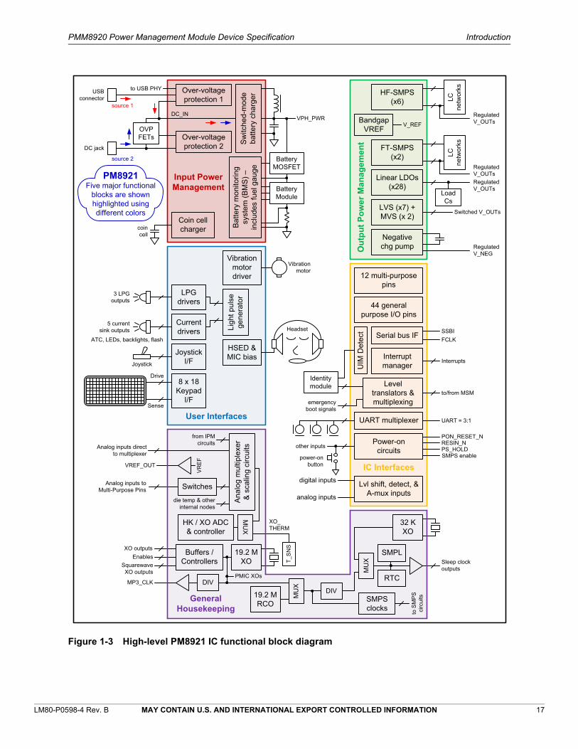
1.6.4 User interface features
1.6.4.1 PM8921 die
One programmable, 5 V-tolerant LED drivers (up to 40 mA)
One 5 mA automatic trickle charging (ATC) indicator
One LPG control for external drivers (GPIOs)
Vibration motor driver programmable from 1.2 to 3.1 V in 100 mV increments
External switch detection (supporting headset and flip switches)
Joystick support
1.6.4.2 PM8821 die
Four multipurpose pins that can be configured as digital inputs or outputs; or level-translating bidirectional I/Os
1.6.5 IC-level interface features
1.6.5.1 PM8921 die
SSBI 2.0 for efficient initialization, status, and control
Three internal interrupt managers (secure and user)
Many functions monitored and reported through realtime and interrupt status signals
Dedicated circuits for controlled power sequencing
Several events continuously monitored for triggering power-on/power-off sequences
Dedicated control settings for selecting optional PMIC hardware configurations
SSBI clock input from the APQ device allows communications even when the PMIC XO is off
Supports and orchestrates soft resets
External controls (via GPIOs) for enabling external regulators
3:1 UART multiplexer (via GPIOs)
UIM detection (via GPIO) and UIM level translators (via MPPs and GPIOs) enable modem IC interfacing with external modules

PMM8920 Power Management Module Device Specification Introduction
LM80-P0598-4 Rev. B MAY CONTAIN U.S. AND INTERNATIONAL EXPORT CONTROLLED INFORMATION 22
1.6.5.2 PM8821 die
Single-wire serial bus interface (SSBI) for efficient initialization, status, and control With backwards compatible SSBI1.0 mode (default at power-up)
Alternate SSBI clock input from the APQ device allows communications even when XO is off
Interrupt manager with single interrupt request output to the APQ device
Dedicated circuits for power sequencing, coordinated by the PM8921
Power control inputs from external devices allows output voltages to be enabled and disabled on demand, thereby reducing quiescent current
MPP4 on the PM8821 die is internally connected to PM8920 XO_OUT_D0_EN pin
1.6.6 Configurable I/O features
1.6.6.1 PM8921 die
Twelve MPPs that can be configured as digital inputs or outputs; level-translating bidirectional I/Os; analog multiplexer inputs; or buffered VREF analog outputs
26 general purpose input/output pins that can be configured as digital inputs or outputs or level-translating I/Os; these configurable I/Os are much faster than MPPs
1.6.6.2 PM8821 die
Three MPPs that can be configured as digital inputs or outputs or level-translating bidirectional I/Os
1.6.7 Package features
Two power-management die integrated into a small package – 13.9 × 12.3 × 1.29 mm
255-pin FBGA with several ground pins for electrical ground, mechanical stability, and thermal relief
PMM8920 Power Management Module Device Specification Introduction
LM80-P0598-4 Rev. B MAY CONTAIN U.S. AND INTERNATIONAL EXPORT CONTROLLED INFORMATION 23
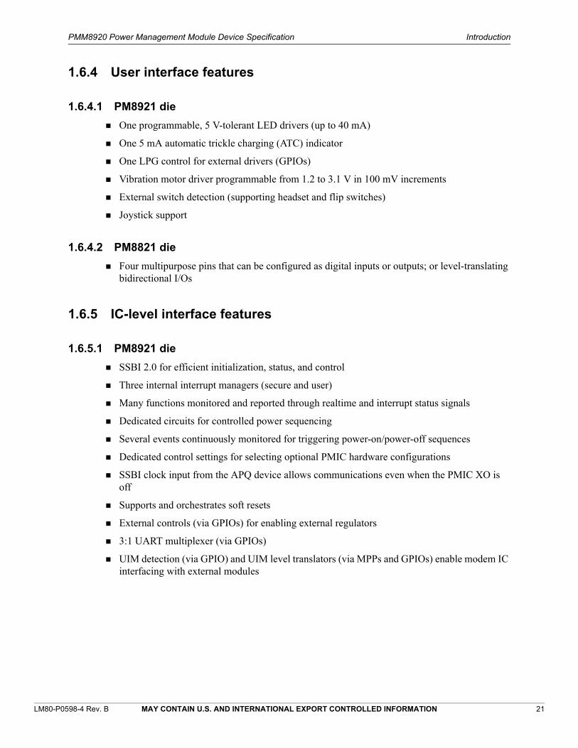
1.6.8 Summary of key PMM8920 features
Table 1-2 Key PMM8920 features
Feature PMM8920 capability
Input power management
Supported external power sources USB and/or wall charger
Over-voltage protection
USB
Wall charger
Fully integrated up to +30 V (integrated OVP FET)
Up to +30 V with external OVP FET
Supported battery technologies Lithium-ion, lithium-ion polymer
Charger regulation method Efficient switched-mode battery charger
Four control loops: USB input current
DC_IN input voltage
VPH_PWR output voltage
Battery current
Supported charging modes Trickle, constant current, and constant voltage modes
More automated for less software interaction
ATC indicator supply ATC LED supply; supplements ATC current driver
External battery MOSFET Optional
Voltage, current and thermal sensors
Internal and external nodes; reported to on-chip state machine
Battery monitoring system Including battery fuel gauge for better accuracy
Coin-cell or capacitor backup Keep-alive power source
Output power management
Buck SMPS
PM8921 die
PM8821 die
7 SMPS circuits; 5 HF-SMPS @ 1.5 A, 2 FT-SMPS @ 2.0 A
2 FT-SMPS circuits @ 2.0 A
LDOs
PM8921 die
PM8821 die
20: 5 @ 1.2 A, 2 @ 600 mA, 4 @ 300 mA; 7 @150 mA; 2 @ 50 mA
1: 50 mA on-die
Voltage switching
PM8921 die
Low-voltage
Medium-voltage
PM8821 die
Gate power to external circuits; limits in-rush current & overcurrent
7: to 1.8 V
2: to 5.0 V
none
Power control from external devices Allows Bluetooth (BT), WLAN, etc., to enable sets of regulators
External voltage-source enables Enable external SMPS circuits like a +5 V boost converter
General HK
On-chip ADC Shared HK and XO support

PMM8920 Power Management Module Device Specification Introduction
LM80-P0598-4 Rev. B MAY CONTAIN U.S. AND INTERNATIONAL EXPORT CONTROLLED INFORMATION 24
Analog multiplexing for ADC
HK inputs
XO input
Select from up several inputs including configurable MPPs
Dedicated pin (XO_THERM)
Overtemperature protection Multistage smart thermal control for each die
19.2 MHz oscillator support XO (with on-chip ADC)
XO controller and XO outputs Five sets: Three low-noise outputs and two low-power outputs
Special purpose clock outputs Two extra sleep clocks; 19.2 MHz for HS-USB; 2.4 MHz for MP3
Integrated 32 kHz clock source Sleep clock without external crystal
Buffered VREF outputs Via MPPs
Realtime clock RTC clock circuits and alarms
User interfaces
Current drivers One capable of sinking up to 40 mA; 5 V tolerant
One dedicated ATC indicator (5 mA)
Controls for external current drivers 1 LPG output
Vibration motor driver 1.2 to 3.1 V, in 100 mV increments
Extra features Joystick support
IC-level interfaces
Primary status and control SSBI for each die
Alternate clock from APQ enables SSBI even when PMIC XO is off
Interrupt managers One interrupt on the PM8891 die
Three interrupts on the PM8921 die: secure and user
Optional hardware configurations OPT bits select hardware configuration
Power sequencing Poweron, poweroff, and soft resets; coordination between two die
UIM support Level translations and UIM detection
Extra features External SMPS enable; 3:1 UART multiplexer; USB_ID detection
Configurable I/Os
MPPs
PM8921 die
PM8821 die
12: all configurable as digital inputs or outputs; level-translating bidirectional I/Os; analog multiplexer inputs; or VREF analog outputs
3: all configurable as digital inputs or outputs; level-translating bidirectional I/Os; analog multiplexer inputs; or VREF analog outputs
GPIO pins 26: configurable as digital inputs or outputs or level-translating I/Os; these configurable I/Os are much faster than MPPs
Package
Size 13.9 × 12.3 × 1.29 mm
Pin count and package type 255-pin FBGA
Table 1-2 Key PMM8920 features (cont.)
Feature PMM8920 capability

PMM8920 Power Management Module Device Specification Introduction
LM80-P0598-4 Rev. B MAY CONTAIN U.S. AND INTERNATIONAL EXPORT CONTROLLED INFORMATION 25
1.7 Terms and acronyms
Table 1-3 defines terms and acronyms used throughout this document.
Table 1-3 Terms and acronyms
Term or acronym Definition
ADC Analog-to-digital converter
AVS Adaptive voltage scaling
BT Bluetooth
DVS Dynamic voltage scaling
FT, FT-SMPS Fast transient, fast transient switched-mode power supply
GPIO General-purpose input/output
HAST Highly accelerated stress test
HDMI High-definition multimedia interface
HK Housekeeping
HS-USB High-speed USB
HTOL High-temperature operating life
ID Identification
LDO Low-dropout linear regulator
Li Lithium
LPG Light pulse generator
LSB Least significant bit
LVS Low-voltage switch
MBB Moisture barrier bag
MDM Mobile Data Modem
MPP Multipurpose pin
MSL Moisture-sensitivity level
MUX Multiplexer
MVS Medium-voltage switch
NCP Negative charge pump
OTG On-the-go
PA Power amplifier
PCB Printed circuit board
PFM Pulse-frequency modulation
PM Power management
PSRR Power-supply ripple rejection
PWM Pulse-width modulation
SBI Serial bus interface (3-wire, unless designated as SSBI)
SMPL Sudden momentary power loss

PMM8920 Power Management Module Device Specification Introduction
LM80-P0598-4 Rev. B MAY CONTAIN U.S. AND INTERNATIONAL EXPORT CONTROLLED INFORMATION 26
1.8 Special marks
Table 1-4 defines special marks used in this document.
SMPS Switched-mode power supply (DC-to-DC converter)
SMT Surface mount technology
SnPb Tin/lead
SSBI Single-wire serial bus interface
SSC SMPS step control
SVS Static voltage scaling
TCXO Temperature-compensated crystal oscillator
UART Universal asynchronous receiver-transmitter
UBM Universal Broadcast Modem
UIM User identity module
USB, USB-OTG Universal serial bus, USB on-the-go
VCTCXO Voltage-controlled temperature-compensated crystal oscillator
VPH_PWR Phone power supply (from charger or battery)
WLAN Wireless local area network
XO Crystal oscillator
Table 1-3 Terms and acronyms (cont.)
Term or acronym Definition
Table 1-4 Special marks
Mark Definition
[ ] Brackets ([ ]) sometimes follow a pin, register, or bit name. These brackets enclose a range of numbers. For example, GPIO_INT[7:0] may indicate a range that is 8 bits in length, or DATA[7:0] may refer to eight DATA pins.
_N A suffix of _N indicates an active low signal. For example, PON_RESET_N.
0x0000 Hexadecimal numbers are identified with an x in the number, for example, 0x0000. All numbers are decimal (base 10) unless otherwise specified. Non-obvious binary numbers have the term binary enclosed in parentheses at the end of the number, for example, 0011 (binary).
| A vertical bar in the outside margin of a page indicates that a change was made since the previous revision of this document.

LM80-P0598-4 Rev. B MAY CONTAIN U.S. AND INTERNATIONAL EXPORT CONTROLLED INFORMATION 27
2 Pin Definitions
The PMM8920 module is available in the 255-pin FBGA that includes several ground pins for electrical grounding, mechanical strength, and thermal continuity. See Chapter 4 for package details. A high-level view of the pin assignments is shown in Figure 2-1.

PMM8920 Power Management Module Device Specification Pin Definitions
LM80-P0598-4 Rev. B MAY CONTAIN U.S. AND INTERNATIONAL EXPORT CONTROLLED INFORMATION 28
Figure 2-1 PMM8920 module pin assignments (top view)
Since the text within Figure 2-1 is difficult to read, close-up views of the left and right halves are shown in Figure 2-2 and Figure 2-3, respectively.
1 2 3 4 5 6 7 8 9 10 11 12 13 14 15 16 17
A NC GND_8821_S2
GND_8821_S2
VDD_8821_S2
VDD_8821_S2
GND_8921_XO
VDD_8921_L10_22
VOUT_5VS_OTG
GND_8921_S1
GND_8921_S3
VDD_8921_S2
GND_8921_S2
VDD_8921_S5
VDD_8921_S5
GND_8921_S5
GND_8921_S5 NC A
B NC NC NCPON
_RST_N_8821
XTAL_32K_OUT
XTAL_32K_IN
VREG_8921_L10
VREG_8921_L22
VDD_8921_S1
GND_8921_S3
VREG_8921_S3
PON_RST_N_8921
VREG_8921_S2
VREG_8921_L18
VREG_8921_S5
OPT3_8921
ATC_LED_SRC
B
C NC NC VSW_8821_S2
VSW_8821_S2
VSW_8821_S2
VREG_8921_L1
VDD_8921_L25
VREG_8921_L25
VSW_8921_S1
VDD_8921_S3
VSW_8921_S2
VSW_8921_S2
VSW_8921_S5
VSW_8921_S5
VSW_8921_S5
CBL_PWR0_N
LED_DRV0_N C
D XO_OUT_D0_EN
VREG_8821_S2
VREG_8921_L2
VREG_8921_L12
VOUT_5VS_HDMI
RESIN_NGND_8921_REF
VREG_8921_S1
VSW_8921_S1
VSW_8921_S3
KYPD_PWR_N GPIO_07 MPP_
8921_04MPP_
8921_01 USB_IN AMUX_IN
OVP_SNS D
E MPP_8821_03
SSBI_8821 GND VIN_5VS VREG_
8921_L3 USB_ID GND_8921_XO
VDD_8921_L1_2_12_18
VDD_8921_L24
VSW_8921_S3
MPP_8921_02
MPP_8921_05
MPP_8921_03
MPP_8921_06
USB_OUT
OVP_CTL USB_IN E
F GND MPP_8821_02
VPH_PWR_8821
VREF_XO
XO_OUT_D1
VREG_XO
XO_THERM
XO_OUT_A0
XO_OUT_A1
VREG_8921_L24 GPIO_18 GPIO_19 BAT_ID PA
_THERMCBL_
PWR1_NPHY
_VBUSUSB
_OUT F
G GND NC VREG_8921_L17
VDD_8921_L5_8
_16
VREG_8921_L5
VREG_8921_L8
VDD_8921_L4_14
GND GND GND GPIO_20 GPIO_22 GPIO_33 VIB_DRV_N
GND_8921_DRV
BMS_CSN
VPH_PWR_8921
G
H MPP_8821_01 NC
VDD_ 8921_L21_23_29
VREG_8921_L9
VREG_8921_L11
VDD_8921_L9_11
VIN_8921_LVS2
VREG_8921_L16
GND_8921
_XOBUFGND GND GND GND DC_IN VREG_
8921_L14VPRE_CAP
BAT_FET_N H
JGND_8821_REF
GNDVDD
_8921_L3_15_17
XTAL_19M_OUT
XTAL_19M_IN GPIO_31 XO_OUT
_A2VREG_8921_L4 GND GND GND GND GND DC_IN VDRV_P VBAT VDD_
CDRV J
K NC VREG_8821_S1
VREG_8921_L15 GPIO_26 GPIO_28 GPIO_32 XO_OUT
_D0
VOUT_8921_LVS2
GND_CHG GPIO_23 GPIO_36 GPIO_35 GPIO_39 GPIO_44 VDRV_N BMS
_CSPVREF_
LPDDR2 K
L GND INT_N_8821
VREG_8921_L6 GPIO_29 VREG_
8921_L23
VOUT_8921_LVS3
GPIO_30 VREG_8921_L26
VDD_8921_L27
GPIO_34 GPIO_38 GPIO_42 GPIO_41 MPP_8921_08
GND_CHG_HP VCOIN VSW
_CHG L
M NC NCVDD
_8921_L26
GPIO_27VOUT_8921_LVS4
GND_8921
_XOADC
VOUT_8921_LVS5
VREG_8921_L27
VSW_8921_S7 GPIO_43 GPIO_37 GPIO_40 MPP_
8921_07MPP_
8921_09GND_
CHG_HPSSBI_8921
VSW_CHG M
N VREG_8921_L7 NC VSW_
8821_S1VSW_
8821_S1VSW_
8821_S1
VOUT_8921_LVS6
VOUT_8921_LVS1
VDD_8921_L28
VSW_8921_S7
VSW_8921_S4
VSW_8921_S4 GND VSW_
8921_S6VSW_
8921_S6VSW_
8921_S6MPP_
8921_12BAT_
THERM N
PVDD
_8921_L6_7
NC NC SLEEP_CLK0
INT_MDM_N_8921
INT_USR_N_8921
VREG_8921_S7
VOUT_8921_LVS7
VDD_8921_S7
VREF_BAT
VREG_8921_S4
INT_SEC_N _8921
PS_HOLD
MPP_8921_10
VREG_8921_S6
MPP_8921_11
GND_CHG_HP P
R NC GND_8821_S1
GND_8821_S1
VDD_8821_S1
VDD_8821_S1
VIN_8921_LVS1_3_6
VIN_8921_LVS4_5_7
VREG_8921_L28 GPIO_05 GND_
8921_S7
VDD_8921_S4
GND_8921_S4
VDD_8921_S6
VDD_8921_S6
GND_8921_S6
GND_8921_S6
GND_CHG_HP R
1 2 3 4 5 6 7 8 9 10 11 12 13 14 15 16 17
Input Power Management
Ouput Power Management
General Housekeeping User Interface IC Interface GPIO or MPP NC Power Ground

PMM8920 Power Management Module Device Specification Pin Definitions
LM80-P0598-4 Rev. B MAY CONTAIN U.S. AND INTERNATIONAL EXPORT CONTROLLED INFORMATION 29
Figure 2-2 Pin assignments – left half
1 2 3 4 5 6 7 8 9
A NC GND_8821_S2
GND_8821_S2
VDD_8821_S2
VDD_8821_S2
GND_8921_XO
VDD_8921_L10_22
VOUT_5VS_OTG
GND_8921_S1 A
B NC NC NCPON
_RST_N_8821
XTAL_32K_OUT
XTAL_32K_IN
VREG_8921_L10
VREG_8921_L22
VDD_8921_S1 B
C NC NC VSW_8821_S2
VSW_8821_S2
VSW_8821_S2
VREG_8921_L1
VDD_8921_L25
VREG_8921_L25
VSW_8921_S1 C
D XO_OUT_D0_EN
VREG_8821_S2
VREG_8921_L2
VREG_8921_L12
VOUT_5VS_HDMI
RESIN_NGND_8921_REF
VREG_8921_S1
VSW_8921_S1 D
E MPP_8821_03
SSBI_8821 GND VIN_5VS VREG_
8921_L3 USB_ID GND_8921_XO
VDD_8921_L1_2_12_18
VDD_8921_L24 E
F GND MPP_8821_02
VPH_PWR_8821
VREF_XO
XO_OUT_D1
VREG_XO
XO_THERM
XO_OUT_A0
XO_OUT_A1 F
G GND NC VREG_8921_L17
VDD_8921_L5_8
_16
VREG_8921_L5
VREG_8921_L8
VDD_8921_L4_14
GND GND G
H MPP_8821_01 NC
VDD_ 8921_L21_23_29
VREG_8921_L9
VREG_8921_L11
VDD_8921_L9_11
VIN_8921_LVS2
VREG_8921_L16
GND_8921
_XOBUFH
JGND_8821_REF
GNDVDD
_8921_L3_15_17
XTAL_19M_OUT
XTAL_19M_IN GPIO_31 XO_OUT
_A2VREG_8921_L4 GND J
K NC VREG_8821_S1
VREG_8921_L15 GPIO_26 GPIO_28 GPIO_32 XO_OUT
_D0
VOUT_8921_LVS2
GND_CHG K
L GND INT_N_8821
VREG_8921_L6 GPIO_29 VREG_
8921_L23
VOUT_8921_LVS3
GPIO_30 VREG_8921_L26
VDD_8921_L27
L
M NC NCVDD
_8921_L26
GPIO_27VOUT_8921_LVS4
GND_8921
_XOADC
VOUT_8921_LVS5
VREG_8921_L27
VSW_8921_S7 M
N VREG_8921_L7 NC VSW_
8821_S1VSW_
8821_S1VSW_
8821_S1
VOUT_8921_LVS6
VOUT_8921_LVS1
VDD_8921_L28
VSW_8921_S7 N
PVDD
_8921_L6_7
NC NC SLEEP_CLK0
INT_MDM_N_8921
INT_USR_N_8921
VREG_8921_S7
VOUT_8921_LVS7
VDD_8921_S7
P
R NC GND_8821_S1
GND_8821_S1
VDD_8821_S1
VDD_8821_S1
VIN_8921_LVS1_3_6
VIN_8921_LVS4_5_7
VREG_8921_L28 GPIO_05 R
1 2 3 4 5 6 7 8 9
Input Power Management
Ouput Power Management
General Housekeeping
User Interface
IC Interface
GPIO or MPP
NC
Power
Ground
PMM8920 Power Management Module Device Specification Pin Definitions
LM80-P0598-4 Rev. B MAY CONTAIN U.S. AND INTERNATIONAL EXPORT CONTROLLED INFORMATION 30
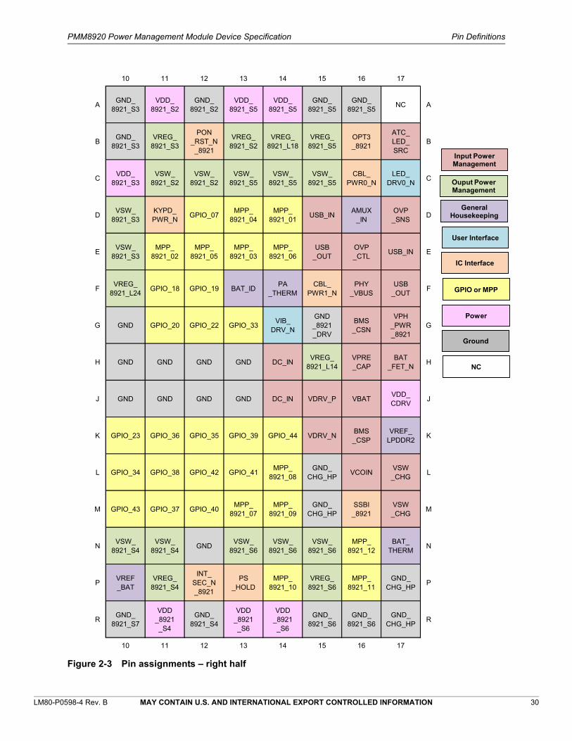
Figure 2-3 Pin assignments – right half
10 11 12 13 14 15 16 17
A GND_8921_S3
VDD_8921_S2
GND_8921_S2
VDD_8921_S5
VDD_8921_S5
GND_8921_S5
GND_8921_S5 NC A
B GND_8921_S3
VREG_8921_S3
PON_RST_N_8921
VREG_8921_S2
VREG_8921_L18
VREG_8921_S5
OPT3_8921
ATC_LED_SRC
B
C VDD_8921_S3
VSW_8921_S2
VSW_8921_S2
VSW_8921_S5
VSW_8921_S5
VSW_8921_S5
CBL_PWR0_N
LED_DRV0_N C
D VSW_8921_S3
KYPD_PWR_N GPIO_07 MPP_
8921_04MPP_
8921_01 USB_IN AMUX_IN
OVP_SNS D
E VSW_8921_S3
MPP_8921_02
MPP_8921_05
MPP_8921_03
MPP_8921_06
USB_OUT
OVP_CTL USB_IN E
F VREG_8921_L24 GPIO_18 GPIO_19 BAT_ID PA
_THERMCBL_
PWR1_NPHY
_VBUSUSB
_OUT F
G GND GPIO_20 GPIO_22 GPIO_33 VIB_DRV_N
GND_8921_DRV
BMS_CSN
VPH_PWR_8921
G
H GND GND GND GND DC_IN VREG_8921_L14
VPRE_CAP
BAT_FET_N H
J GND GND GND GND DC_IN VDRV_P VBAT VDD_CDRV J
K GPIO_23 GPIO_36 GPIO_35 GPIO_39 GPIO_44 VDRV_N BMS_CSP
VREF_LPDDR2 K
L GPIO_34 GPIO_38 GPIO_42 GPIO_41 MPP_8921_08
GND_CHG_HP VCOIN VSW
_CHG L
M GPIO_43 GPIO_37 GPIO_40 MPP_8921_07
MPP_8921_09
GND_CHG_HP
SSBI_8921
VSW_CHG M
N VSW_8921_S4
VSW_8921_S4 GND VSW_
8921_S6VSW_
8921_S6VSW_
8921_S6MPP_
8921_12BAT_
THERM N
P VREF_BAT
VREG_8921_S4
INT_SEC_N _8921
PS_HOLD
MPP_8921_10
VREG_8921_S6
MPP_8921_11
GND_CHG_HP P
R GND_8921_S7
VDD_8921_S4
GND_8921_S4
VDD_8921_S6
VDD_8921_S6
GND_8921_S6
GND_8921_S6
GND_CHG_HP R
10 11 12 13 14 15 16 17
Input Power Management
Ouput Power Management
General Housekeeping
User Interface
IC Interface
GPIO or MPP
NC
Power
Ground
PMM8920 Power Management Module Device Specification Pin Definitions
LM80-P0598-4 Rev. B MAY CONTAIN U.S. AND INTERNATIONAL EXPORT CONTROLLED INFORMATION 31
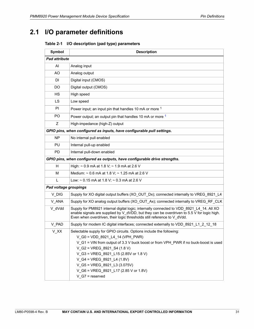
2.1 I/O parameter definitions
Table 2-1 I/O description (pad type) parameters
Symbol Description
Pad attribute
AI Analog input
AO Analog output
DI Digital input (CMOS)
DO Digital output (CMOS)
HS High speed
LS Low speed
PI Power input; an input pin that handles 10 mA or more 1
PO Power output; an output pin that handles 10 mA or more 1
Z High-impedance (high-Z) output
GPIO pins, when configured as inputs, have configurable pull settings.
NP No internal pull enabled
PU Internal pull-up enabled
PD Internal pull-down enabled
GPIO pins, when configured as outputs, have configurable drive strengths.
H High: ~ 0.9 mA at 1.8 V; ~ 1.9 mA at 2.6 V
M Medium: ~ 0.6 mA at 1.8 V; ~ 1.25 mA at 2.6 V
L Low: ~ 0.15 mA at 1.8 V; ~ 0.3 mA at 2.6 V
Pad voltage groupings
V_DIG Supply for XO digital output buffers (XO_OUT_Dx); connected internally to VREG_8921_L4
V_ANA Supply for XO analog output buffers (XO_OUT_Ax); connected internally to VREG_RF_CLK
V_dVdd Supply for PM8921 internal digital logic; internally connected to VDD_8921_L4_14. All XO enable signals are supplied by V_dVDD, but they can be overdriven to 5.5 V for logic high. Even when overdriven, their logic thresholds still reference to V_dVdd.
V_PAD Supply for modem IC digital interfaces; connected externally to VDD_8921_L1_2_12_18
V_XX Selectable supply for GPIO circuits. Options include the following:
V_G0 = VDD_8921_L4_14 (VPH_PWR)
V_G1 = VIN from output of 3.3 V buck boost or from VPH_PWR if no buck-boost is used
V_G2 = VREG_8921_S4 (1.8 V)
V_G3 = VREG_8921_L15 (2.85V or 1.8 V)
V_G4 = VREG_8921_L4 (1.8V)
V_G5 = VREG_8921_L3 (3.075V)
V_G6 = VREG_8921_L17 (2.85 V or 1.8V)
V_G7 = reserved
PMM8920 Power Management Module Device Specification Pin Definitions
LM80-P0598-4 Rev. B MAY CONTAIN U.S. AND INTERNATIONAL EXPORT CONTROLLED INFORMATION 32
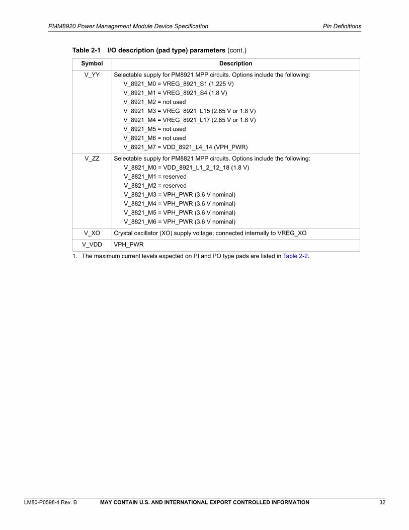
V_YY Selectable supply for PM8921 MPP circuits. Options include the following:
V_8921_M0 = VREG_8921_S1 (1.225 V)
V_8921_M1 = VREG_8921_S4 (1.8 V)
V_8921_M2 = not used
V_8921_M3 = VREG_8921_L15 (2.85 V or 1.8 V)
V_8921_M4 = VREG_8921_L17 (2.85 V or 1.8 V)
V_8921_M5 = not used
V_8921_M6 = not used
V_8921_M7 = VDD_8921_L4_14 (VPH_PWR)
V_ZZ Selectable supply for PM8821 MPP circuits. Options include the following:
V_8821_M0 = VDD_8921_L1_2_12_18 (1.8 V)
V_8821_M1 = reserved
V_8821_M2 = reserved
V_8821_M3 = VPH_PWR (3.6 V nominal)
V_8821_M4 = VPH_PWR (3.6 V nominal)
V_8821_M5 = VPH_PWR (3.6 V nominal)
V_8821_M6 = VPH_PWR (3.6 V nominal)
V_XO Crystal oscillator (XO) supply voltage; connected internally to VREG_XO
V_VDD VPH_PWR
1. The maximum current levels expected on PI and PO type pads are listed in Table 2-2.
Table 2-1 I/O description (pad type) parameters (cont.)
Symbol Description

PMM8920 Power Management Module Device Specification Pin Definitions
LM80-P0598-4 Rev. B MAY CONTAIN U.S. AND INTERNATIONAL EXPORT CONTROLLED INFORMATION 33
Table 2-2 Expected maximum currents at PI and PO pad types
Pad # Function TypeCurrent (mA) 2
2. Listed current is the expected maximum.
| Pad # Function TypeCurrent (mA) 2
C17 LED_DRV0_N PI 40 | H5 VREG_8921_L11 PO 150
N7 VOUT_8921_LVS1 PO 100 | D4 VREG_8921_L12 PO 150
K8 VOUT_8921_LVS2 PO 300 | H15 VREG_8921_L14 PO 50
L6 VOUT_8921_LVS3 PO 100 K3 VREG_8921_L15 PO 150
M5 VOUT_8921_LVS4 PO 100 | H8 VREG_8921_L16 PO 300
M7 VOUT_8921_LVS5 PO 100 | G3 VREG_8921_L17 PO 150
N6 VOUT_8921_LVS6 PO 100 | B14 VREG_8921_L18 PO 150
P8 VOUT_8921_LVS7 PO 100 | B8 VREG_8921_L22 PO 150
A8 VOUT_5VS_OTG PO 500 | L5 VREG_8921_L23 PO 150
D5 VOUT_5VS_HMDI PO 62 | F10 VREG_8921_L24 PO 1200
F6 VREG_XO PO 50 | C8 VREG_8921_L25 PO 1200
C6 VREG_8921_L1 PO 150 | L8 VREG_8921_L26 PO 1200
D3 VREG_8921_L2 PO 150 | M8 VREG_8921_L27 PO 1200
E5 VREG_8921_L3 1
1. VREG_8921_L3 is used as the USB_LDO is a conventional PMOD LDO (150 mA). VIN of this LDO is tied to VPH_PWR. Effective rated current is reduced to 50 mA to lower drop-out voltage by a factor of 3.
PO 150 | R8 VREG_8921_L28 PO 1200
J8 VREG_8921_L4 PO 50 | N3, N4, N5 VSW_8821_S1 PO 2000
G5 VREG_8921_L5 PO 300 | C3, C4, C5 VSW_8821_S2 PO 1500
L3 VREG_8921_L6 PO 600 | C9, D9 VSW_8921_S1 PO 1500
N1 VREG_8921_L7 PO 150 | C11, C12 VSW_8921_S2 PO 1500
G6 VREG_8921_L8 PO 300 | D10, E10 VSW_8921_S3 PO 1500
H4 VREG_8921_L9 PO 300 | N10, N11 VSW_8921_S4 PO 1500
B7 VREG_8921_L10 PO 600 | C13, C14, C15 VSW_8921_S5 PO 2000
| N13, N14, N15 VSW_8921_S6 PO 2000
| M9, N9 VSW_8921_S7 PO 1500
PMM8920 Power Management Module Device Specification Pin Definitions
LM80-P0598-4 Rev. B MAY CONTAIN U.S. AND INTERNATIONAL EXPORT CONTROLLED INFORMATION 34
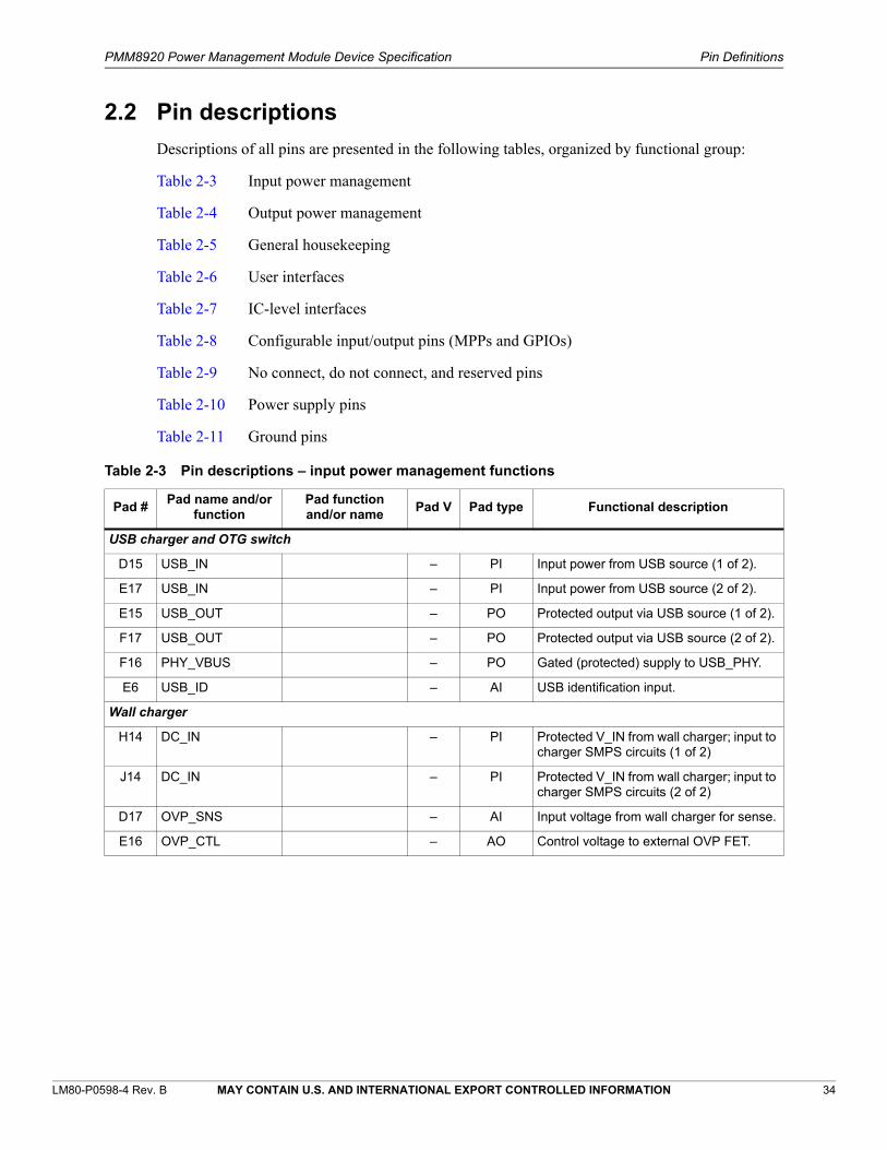
2.2 Pin descriptions
Descriptions of all pins are presented in the following tables, organized by functional group:
Table 2-3 Input power management
Table 2-4 Output power management
Table 2-5 General housekeeping
Table 2-6 User interfaces
Table 2-7 IC-level interfaces
Table 2-8 Configurable input/output pins (MPPs and GPIOs)
Table 2-9 No connect, do not connect, and reserved pins
Table 2-10 Power supply pins
Table 2-11 Ground pins
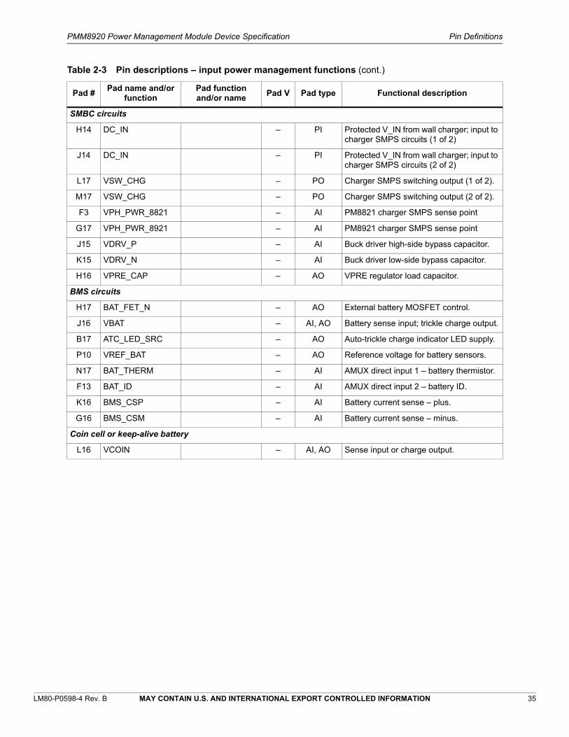
Table 2-3 Pin descriptions – input power management functions
Pad #Pad name and/or
functionPad function and/or name
Pad V Pad type Functional description
USB charger and OTG switch
D15 USB_IN – PI Input power from USB source (1 of 2).
E17 USB_IN – PI Input power from USB source (2 of 2).
E15 USB_OUT – PO Protected output via USB source (1 of 2).
F17 USB_OUT – PO Protected output via USB source (2 of 2).
F16 PHY_VBUS – PO Gated (protected) supply to USB_PHY.
E6 USB_ID – AI USB identification input.
Wall charger
H14 DC_IN – PI Protected V_IN from wall charger; input to charger SMPS circuits (1 of 2)
J14 DC_IN – PI Protected V_IN from wall charger; input to charger SMPS circuits (2 of 2)
D17 OVP_SNS – AI Input voltage from wall charger for sense.
E16 OVP_CTL – AO Control voltage to external OVP FET.
PMM8920 Power Management Module Device Specification Pin Definitions
LM80-P0598-4 Rev. B MAY CONTAIN U.S. AND INTERNATIONAL EXPORT CONTROLLED INFORMATION 35
SMBC circuits
H14 DC_IN – PI Protected V_IN from wall charger; input to charger SMPS circuits (1 of 2)
J14 DC_IN – PI Protected V_IN from wall charger; input to charger SMPS circuits (2 of 2)
L17 VSW_CHG – PO Charger SMPS switching output (1 of 2).
M17 VSW_CHG – PO Charger SMPS switching output (2 of 2).
F3 VPH_PWR_8821 – AI PM8821 charger SMPS sense point
G17 VPH_PWR_8921 – AI PM8921 charger SMPS sense point
J15 VDRV_P – AI Buck driver high-side bypass capacitor.
K15 VDRV_N – AI Buck driver low-side bypass capacitor.
H16 VPRE_CAP – AO VPRE regulator load capacitor.
BMS circuits
H17 BAT_FET_N – AO External battery MOSFET control.
J16 VBAT – AI, AO Battery sense input; trickle charge output.
B17 ATC_LED_SRC – AO Auto-trickle charge indicator LED supply.
P10 VREF_BAT – AO Reference voltage for battery sensors.
N17 BAT_THERM – AI AMUX direct input 1 – battery thermistor.
F13 BAT_ID – AI AMUX direct input 2 – battery ID.
K16 BMS_CSP – AI Battery current sense – plus.
G16 BMS_CSM – AI Battery current sense – minus.
Coin cell or keep-alive battery
L16 VCOIN – AI, AO Sense input or charge output.
Table 2-3 Pin descriptions – input power management functions (cont.)
Pad #Pad name and/or
functionPad function and/or name
Pad V Pad type Functional description
PMM8920 Power Management Module Device Specification Pin Definitions
LM80-P0598-4 Rev. B MAY CONTAIN U.S. AND INTERNATIONAL EXPORT CONTROLLED INFORMATION 36
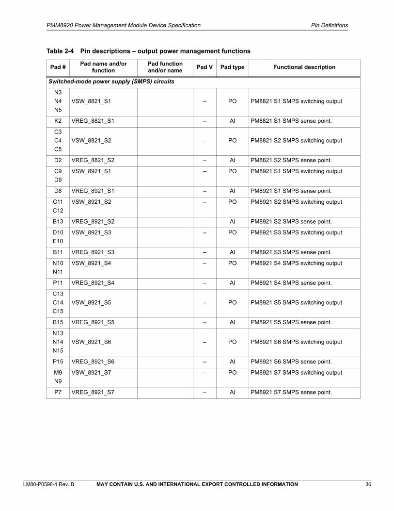
Table 2-4 Pin descriptions – output power management functions
Pad #Pad name and/or
functionPad function and/or name
Pad V Pad type Functional description
Switched-mode power supply (SMPS) circuits
N3
N4
N5
VSW_8821_S1 – PO PM8821 S1 SMPS switching output
K2 VREG_8821_S1 – AI PM8821 S1 SMPS sense point.
C3
C4
C5
VSW_8821_S2 – PO PM8821 S2 SMPS switching output
D2 VREG_8821_S2 – AI PM8821 S2 SMPS sense point.
C9
D9
VSW_8921_S1 – PO PM8921 S1 SMPS switching output
D8 VREG_8921_S1 – AI PM8921 S1 SMPS sense point.
C11
C12
VSW_8921_S2 – PO PM8921 S2 SMPS switching output
B13 VREG_8921_S2 – AI PM8921 S2 SMPS sense point.
D10
E10
VSW_8921_S3 – PO PM8921 S3 SMPS switching output
B11 VREG_8921_S3 – AI PM8921 S3 SMPS sense point.
N10
N11
VSW_8921_S4 – PO PM8921 S4 SMPS switching output
P11 VREG_8921_S4 – AI PM8921 S4 SMPS sense point.
C13
C14
C15
VSW_8921_S5 – PO PM8921 S5 SMPS switching output
B15 VREG_8921_S5 – AI PM8921 S5 SMPS sense point.
N13
N14
N15
VSW_8921_S6 – PO PM8921 S6 SMPS switching output
P15 VREG_8921_S6 – AI PM8921 S6 SMPS sense point.
M9
N9
VSW_8921_S7 – PO PM8921 S7 SMPS switching output
P7 VREG_8921_S7 – AI PM8921 S7 SMPS sense point.
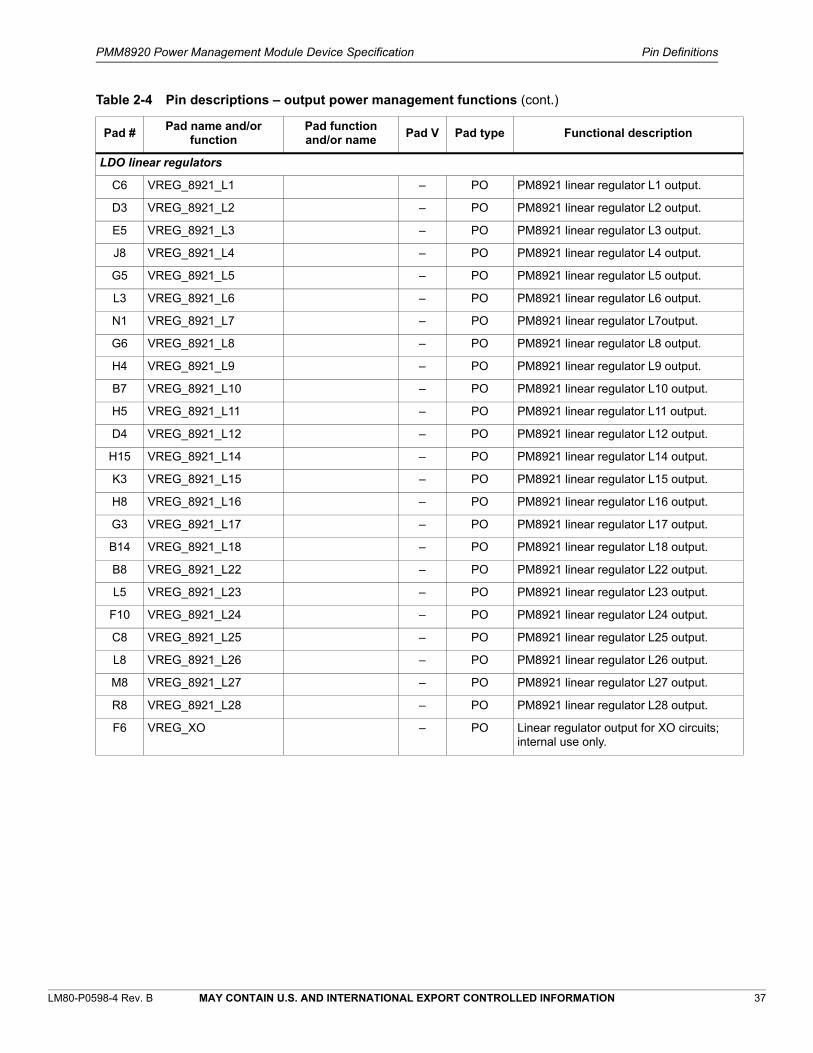
PMM8920 Power Management Module Device Specification Pin Definitions
LM80-P0598-4 Rev. B MAY CONTAIN U.S. AND INTERNATIONAL EXPORT CONTROLLED INFORMATION 37
LDO linear regulators
C6 VREG_8921_L1 – PO PM8921 linear regulator L1 output.
D3 VREG_8921_L2 – PO PM8921 linear regulator L2 output.
E5 VREG_8921_L3 – PO PM8921 linear regulator L3 output.
J8 VREG_8921_L4 – PO PM8921 linear regulator L4 output.
G5 VREG_8921_L5 – PO PM8921 linear regulator L5 output.
L3 VREG_8921_L6 – PO PM8921 linear regulator L6 output.
N1 VREG_8921_L7 – PO PM8921 linear regulator L7output.
G6 VREG_8921_L8 – PO PM8921 linear regulator L8 output.
H4 VREG_8921_L9 – PO PM8921 linear regulator L9 output.
B7 VREG_8921_L10 – PO PM8921 linear regulator L10 output.
H5 VREG_8921_L11 – PO PM8921 linear regulator L11 output.
D4 VREG_8921_L12 – PO PM8921 linear regulator L12 output.
H15 VREG_8921_L14 – PO PM8921 linear regulator L14 output.
K3 VREG_8921_L15 – PO PM8921 linear regulator L15 output.
H8 VREG_8921_L16 – PO PM8921 linear regulator L16 output.
G3 VREG_8921_L17 – PO PM8921 linear regulator L17 output.
B14 VREG_8921_L18 – PO PM8921 linear regulator L18 output.
B8 VREG_8921_L22 – PO PM8921 linear regulator L22 output.
L5 VREG_8921_L23 – PO PM8921 linear regulator L23 output.
F10 VREG_8921_L24 – PO PM8921 linear regulator L24 output.
C8 VREG_8921_L25 – PO PM8921 linear regulator L25 output.
L8 VREG_8921_L26 – PO PM8921 linear regulator L26 output.
M8 VREG_8921_L27 – PO PM8921 linear regulator L27 output.
R8 VREG_8921_L28 – PO PM8921 linear regulator L28 output.
F6 VREG_XO – PO Linear regulator output for XO circuits; internal use only.
Table 2-4 Pin descriptions – output power management functions (cont.)
Pad #Pad name and/or
functionPad function and/or name
Pad V Pad type Functional description
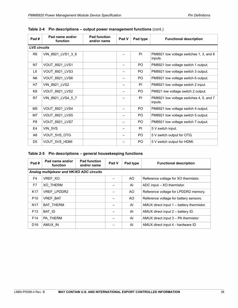
PMM8920 Power Management Module Device Specification Pin Definitions
LM80-P0598-4 Rev. B MAY CONTAIN U.S. AND INTERNATIONAL EXPORT CONTROLLED INFORMATION 38
LVS circuits
R6 VIN_8921_LVS1_3_6 – PI PM8921 low voltage switches 1, 3, and 6 inputs.
N7 VOUT_8921_LVS1 – PO PM8921 low voltage switch 1 output.
L6 VOUT_8921_LVS3 – PO PM8921 low voltage switch 3 output.
N6 VOUT_8921_LVS6 – PO PM8921 low voltage switch 6 output.
H7 VIN_8921_LVS2 – PI PM8921 low voltage switch 2 input.
K8 VOUT_8921_LVS2 – PO PM821 low voltage switch 2 output.
R7 VIN_8921_LVS4_5_7 – PI PM8921 low voltage switches 4, 5, and 7 inputs.
M5 VOUT_8921_LVS4 – PO PM8921 low voltage switch 4 output.
M7 VOUT_8921_LVS5 – PO PM8921 low voltage switch 5 output.
P8 VOUT_8921_LVS7 – PO PM8921 low voltage switch 7 output.
E4 VIN_5VS – PI 5 V switch input.
A8 VOUT_5VS_OTG – PO 5 V switch output for OTG.
D5 VOUT_5VS_HDMI – PO 5 V switch output for HDMI.
Table 2-4 Pin descriptions – output power management functions (cont.)
Pad #Pad name and/or
functionPad function and/or name
Pad V Pad type Functional description
Table 2-5 Pin descriptions – general housekeeping functions
Pad #Pad name and/or
functionPad function and/or name
Pad V Pad type Functional description
Analog multiplexer and HK/XO ADC circuits
F4 VREF_XO – AO Reference voltage for XO thermistor.
F7 XO_THERM – AI ADC input – XO thermistor.
K17 VREF_LPDDR2 – AO Reference voltage for LPDDR2 memory.
P10 VREF_BAT – AO Reference voltage for battery sensors.
N17 BAT_THERM – AI AMUX direct input 1 – battery thermistor.
F13 BAT_ID – AI AMUX direct input 2 – battery ID.
F14 PA_THERM – AI AMUX direct input 3 – PA thermistor.
D16 AMUX_IN – AI AMUX direct input 4 - hardware ID
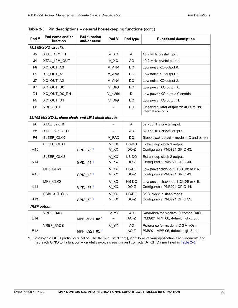
PMM8920 Power Management Module Device Specification Pin Definitions
LM80-P0598-4 Rev. B MAY CONTAIN U.S. AND INTERNATIONAL EXPORT CONTROLLED INFORMATION 39
19.2 MHz XO circuits
J5 XTAL_19M_IN V_XO AI 19.2 MHz crystal input.
J4 XTAL_19M_OUT V_XO AO 19.2 MHz crystal output.
F8 XO_OUT_A0 V_ANA DO Low noise XO output 0.
F9 XO_OUT_A1 V_ANA DO Low noise XO output 1.
J7 XO_OUT_A2 V_ANA DO Low noise XO output 2.
K7 XO_OUT_D0 V_DIG DO Low power XO output 0.
D1 XO_OUT_D0_EN V_dVdd DI Low power XO output 0 enable.
F5 XO_OUT_D1 V_DIG DO Low power XO output 1.
F6 VREG_XO – PO Linear regulator output for XO circuits; internal use only.
32.768 kHz XTAL, sleep clock, and MP3 clock circuits
B6 XTAL_32K_IN – AI 32.768 kHz crystal input.
B5 XTAL_32K_OUT – AO 32.768 kHz crystal output.
P4 SLEEP_CLK0 V_PAD DO Sleep clock output – modem IC and others.
M10
SLEEP_CLK1
GPIO_43 1V_XX
V_XX
LS-DO
DO-Z
Extra sleep clock 1 output.
Configurable PM8921 GPIO 43.
K14
SLEEP_CLK2
GPIO_44 1V_XX
V_XX
LS-DO
DO-Z
Extra sleep clock 2 output.
Configurable PM8921 GPIO 44.
M10
MP3_CLK1
GPIO_43 1V_XX
V_XX
HS-DO
DO-Z
Low power clock out; TCXO/8 or /16.
Configurable PM8921 GPIO 43.
K14
MP3_CLK2
GPIO_44 1V_XX
V_XX
HS-DO
DO-Z
Low power clock out; TCXO/8 or /16.
Configurable PM8921 GPIO 44.
K13
SSBI_ALT_CLK
GPIO_39 1V_XX
V_XX
HS-DO
DO-Z
SSBI clock in sleep mode
Configurable PM8921 GPIO 39.
VREF output
E14
VREF_DAC
MPP_8921_06 1 V_YY
–
AO
AO-Z
Reference for modem IC combo DAC.
PM8921 MPP 06; default high-Z out.
E12
VREF_PADS
MPP_8921_05 1V_YY
–
AO
AO-Z
Reference for modem IC 3 V I/Os.
PM8921 MPP 05; default high-Z out.
1. To assign a GPIO particular function (like the one listed here), identify all of your application’s requirements and map each GPIO to its function – carefully avoiding assignment conflicts. All GPIOs are listed in Table 2-8.
Table 2-5 Pin descriptions – general housekeeping functions (cont.)
Pad #Pad name and/or
functionPad function and/or name
Pad V Pad type Functional description
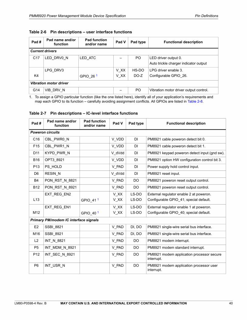
PMM8920 Power Management Module Device Specification Pin Definitions
LM80-P0598-4 Rev. B MAY CONTAIN U.S. AND INTERNATIONAL EXPORT CONTROLLED INFORMATION 40
Table 2-6 Pin descriptions – user interface functions
Pad #Pad name and/or
functionPad function and/or name
Pad V Pad type Functional description
Current drivers
C17 LED_DRV0_N LED_ATC – PO LED driver output 0.
Auto trickle charger indicator output
K4
LPG_DRV3
GPIO_26 1
1. To assign a GPIO particular function (like the one listed here), identify all of your application’s requirements and map each GPIO to its function – carefully avoiding assignment conflicts. All GPIOs are listed in Table 2-8.
V_XX
V_XX
HS-DO
DO-Z
LPG driver enable 3.
Configurable GPIO_26.
Vibration motor driver
G14 VIB_DRV_N – PO Vibration motor driver output control.
Table 2-7 Pin descriptions – IC-level interface functions
Pad #Pad name and/or
functionPad function and/or name
Pad V Pad type Functional description
Poweron circuits
C16 CBL_PWR0_N V_VDD DI PM8921 cable poweron detect bit 0.
F15 CBL_PWR1_N V_VDD DI PM8921 cable poweron detect bit 1.
D11 KYPD_PWR_N V_dVdd DI PM8921 keypad poweron detect input (gnd sw).
B16 OPT3_8921 V_VDD DI PM8921 option HW configuration control bit 3.
P13 PS_HOLD V_PAD DI Power supply hold control input.
D6 RESIN_N V_dVdd DI PM8921 reset input.
B4 PON_RST_N_8821 V_PAD DO PM8821 poweron reset output control.
B12 PON_RST_N_8921 V_PAD DO PM8921 poweron reset output control.
L13
EXT_REG_EN2
GPIO_41 1V_XX
V_XX
LS-DO
LS-DO
External regulator enable 2 at poweron.
Configurable GPIO_41; special default.
M12
EXT_REG_EN1
GPIO_40 1V_XX
V_XX
LS-DO
LS-DO
External regulator enable 1 at poweron.
Configurable GPIO_40; special default.
Primary PM/modem IC interface signals
E2 SSBI_8821 V_PAD DI, DO PM8821 single-wire serial bus interface.
M16 SSBI_8921 V_PAD DI, DO PM8921 single-wire serial bus interface.
L2 INT_N_8821 V_PAD DO PM8821 modem interrupt.
P5 INT_MDM_N_8921 V_PAD DO PM8921 modem standard interrupt.
P12 INT_SEC_N_8921 V_PAD DO PM8921 modem application processor secure interrupt.
P6 INT_USR_N V_PAD DO PM8921 modem application processor user interrupt.
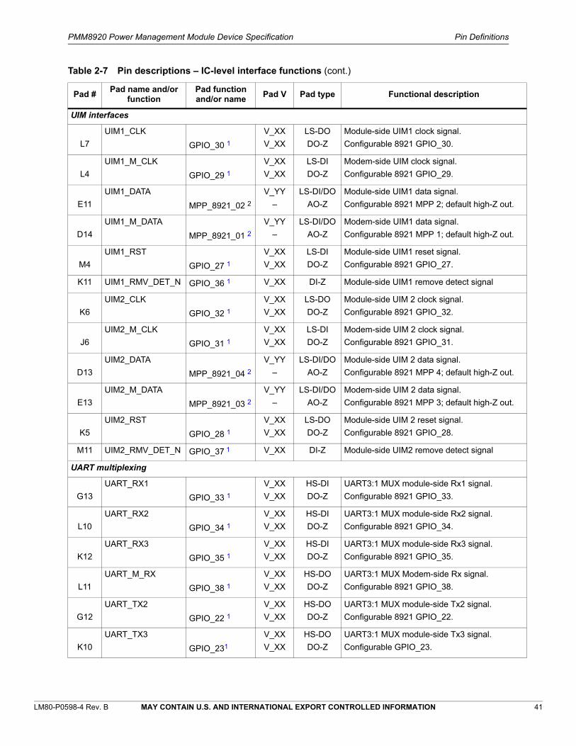
PMM8920 Power Management Module Device Specification Pin Definitions
LM80-P0598-4 Rev. B MAY CONTAIN U.S. AND INTERNATIONAL EXPORT CONTROLLED INFORMATION 41
UIM interfaces
L7
UIM1_CLK
GPIO_30 1V_XX
V_XX
LS-DO
DO-Z
Module-side UIM1 clock signal.
Configurable 8921 GPIO_30.
L4
UIM1_M_CLK
GPIO_29 1V_XX
V_XX
LS-DI
DO-Z
Modem-side UIM clock signal.
Configurable 8921 GPIO_29.
E11
UIM1_DATA
MPP_8921_02 2V_YY
–
LS-DI/DO
AO-Z
Module-side UIM1 data signal.
Configurable 8921 MPP 2; default high-Z out.
D14
UIM1_M_DATA
MPP_8921_01 2V_YY
–
LS-DI/DO
AO-Z
Modem-side UIM1 data signal.
Configurable 8921 MPP 1; default high-Z out.
M4
UIM1_RST
GPIO_27 1V_XX
V_XX
LS-DI
DO-Z
Module-side UIM1 reset signal.
Configurable 8921 GPIO_27.
K11 UIM1_RMV_DET_N GPIO_36 1 V_XX DI-Z Module-side UIM1 remove detect signal
K6
UIM2_CLK
GPIO_32 1V_XX
V_XX
LS-DO
DO-Z
Module-side UIM 2 clock signal.
Configurable 8921 GPIO_32.
J6
UIM2_M_CLK
GPIO_31 1V_XX
V_XX
LS-DI
DO-Z
Modem-side UIM 2 clock signal.
Configurable 8921 GPIO_31.
D13
UIM2_DATA
MPP_8921_04 2V_YY
–
LS-DI/DO
AO-Z
Module-side UIM 2 data signal.
Configurable 8921 MPP 4; default high-Z out.
E13
UIM2_M_DATA
MPP_8921_03 2V_YY
–
LS-DI/DO
AO-Z
Modem-side UIM 2 data signal.
Configurable 8921 MPP 3; default high-Z out.
K5
UIM2_RST
GPIO_28 1V_XX
V_XX
LS-DO
DO-Z
Module-side UIM 2 reset signal.
Configurable 8921 GPIO_28.
M11 UIM2_RMV_DET_N GPIO_37 1 V_XX DI-Z Module-side UIM2 remove detect signal
UART multiplexing
G13
UART_RX1
GPIO_33 1V_XX
V_XX
HS-DI
DO-Z
UART3:1 MUX module-side Rx1 signal.
Configurable 8921 GPIO_33.
L10
UART_RX2
GPIO_34 1V_XX
V_XX
HS-DI
DO-Z
UART3:1 MUX module-side Rx2 signal.
Configurable 8921 GPIO_34.
K12
UART_RX3
GPIO_35 1V_XX
V_XX
HS-DI
DO-Z
UART3:1 MUX module-side Rx3 signal.
Configurable 8921 GPIO_35.
L11
UART_M_RX
GPIO_38 1V_XX
V_XX
HS-DO
DO-Z
UART3:1 MUX Modem-side Rx signal.
Configurable 8921 GPIO_38.
G12
UART_TX2
GPIO_22 1V_XX
V_XX
HS-DO
DO-Z
UART3:1 MUX module-side Tx2 signal.
Configurable 8921 GPIO_22.
K10
UART_TX3
GPIO_231
V_XX
V_XX
HS-DO
DO-Z
UART3:1 MUX module-side Tx3 signal.
Configurable GPIO_23.
Table 2-7 Pin descriptions – IC-level interface functions (cont.)
Pad #Pad name and/or
functionPad function and/or name
Pad V Pad type Functional description
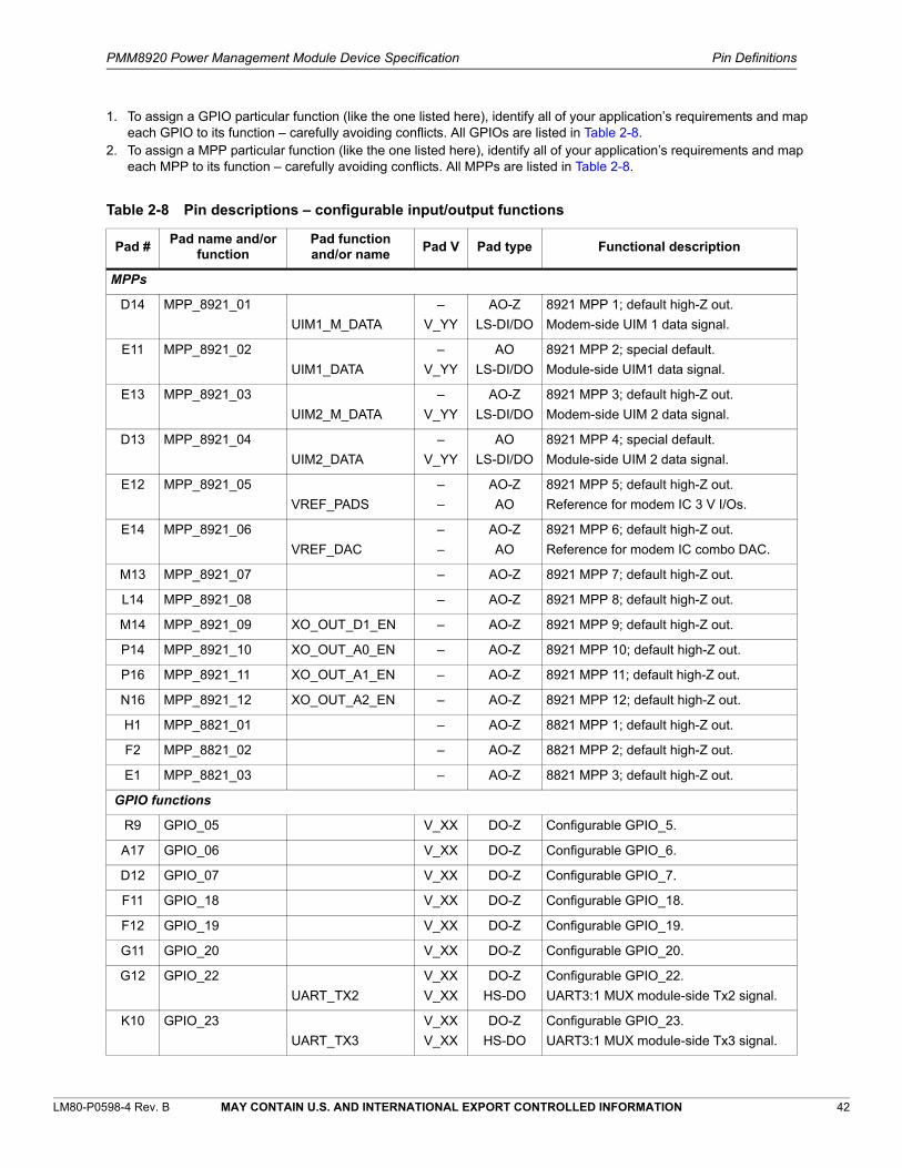
PMM8920 Power Management Module Device Specification Pin Definitions
LM80-P0598-4 Rev. B MAY CONTAIN U.S. AND INTERNATIONAL EXPORT CONTROLLED INFORMATION 42
1. To assign a GPIO particular function (like the one listed here), identify all of your application’s requirements and map each GPIO to its function – carefully avoiding conflicts. All GPIOs are listed in Table 2-8.
2. To assign a MPP particular function (like the one listed here), identify all of your application’s requirements and map each MPP to its function – carefully avoiding conflicts. All MPPs are listed in Table 2-8.
Table 2-8 Pin descriptions – configurable input/output functions
Pad #Pad name and/or
functionPad function and/or name
Pad V Pad type Functional description
MPPs
D14 MPP_8921_01
UIM1_M_DATA
–
V_YY
AO-Z
LS-DI/DO
8921 MPP 1; default high-Z out.
Modem-side UIM 1 data signal.
E11 MPP_8921_02
UIM1_DATA
–
V_YY
AO
LS-DI/DO
8921 MPP 2; special default.
Module-side UIM1 data signal.
E13 MPP_8921_03
UIM2_M_DATA
–
V_YY
AO-Z
LS-DI/DO
8921 MPP 3; default high-Z out.
Modem-side UIM 2 data signal.
D13 MPP_8921_04
UIM2_DATA
–
V_YY
AO
LS-DI/DO
8921 MPP 4; special default.
Module-side UIM 2 data signal.
E12 MPP_8921_05
VREF_PADS
–
–
AO-Z
AO
8921 MPP 5; default high-Z out.
Reference for modem IC 3 V I/Os.
E14 MPP_8921_06
VREF_DAC
–
–
AO-Z
AO
8921 MPP 6; default high-Z out.
Reference for modem IC combo DAC.
M13 MPP_8921_07 – AO-Z 8921 MPP 7; default high-Z out.
L14 MPP_8921_08 – AO-Z 8921 MPP 8; default high-Z out.
M14 MPP_8921_09 XO_OUT_D1_EN – AO-Z 8921 MPP 9; default high-Z out.
P14 MPP_8921_10 XO_OUT_A0_EN – AO-Z 8921 MPP 10; default high-Z out.
P16 MPP_8921_11 XO_OUT_A1_EN – AO-Z 8921 MPP 11; default high-Z out.
N16 MPP_8921_12 XO_OUT_A2_EN – AO-Z 8921 MPP 12; default high-Z out.
H1 MPP_8821_01 – AO-Z 8821 MPP 1; default high-Z out.
F2 MPP_8821_02 – AO-Z 8821 MPP 2; default high-Z out.
E1 MPP_8821_03 – AO-Z 8821 MPP 3; default high-Z out.
GPIO functions
R9 GPIO_05 V_XX DO-Z Configurable GPIO_5.
A17 GPIO_06 V_XX DO-Z Configurable GPIO_6.
D12 GPIO_07 V_XX DO-Z Configurable GPIO_7.
F11 GPIO_18 V_XX DO-Z Configurable GPIO_18.
F12 GPIO_19 V_XX DO-Z Configurable GPIO_19.
G11 GPIO_20 V_XX DO-Z Configurable GPIO_20.
G12 GPIO_22
UART_TX2
V_XX
V_XX
DO-Z
HS-DO
Configurable GPIO_22.
UART3:1 MUX module-side Tx2 signal.
K10 GPIO_23
UART_TX3
V_XX
V_XX
DO-Z
HS-DO
Configurable GPIO_23.
UART3:1 MUX module-side Tx3 signal.
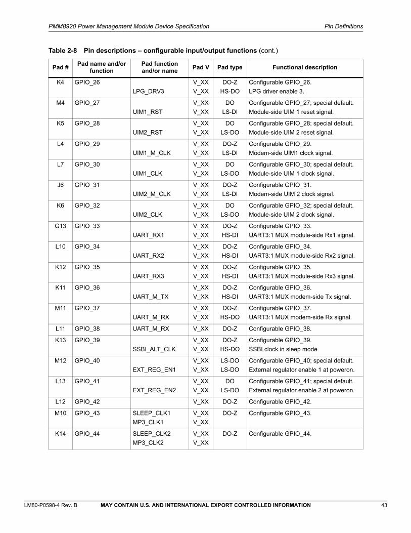
PMM8920 Power Management Module Device Specification Pin Definitions
LM80-P0598-4 Rev. B MAY CONTAIN U.S. AND INTERNATIONAL EXPORT CONTROLLED INFORMATION 43
K4 GPIO_26
LPG_DRV3
V_XX
V_XX
DO-Z
HS-DO
Configurable GPIO_26.
LPG driver enable 3.
M4 GPIO_27
UIM1_RST
V_XX
V_XX
DO
LS-DI
Configurable GPIO_27; special default.
Module-side UIM 1 reset signal.
K5 GPIO_28
UIM2_RST
V_XX
V_XX
DO
LS-DO
Configurable GPIO_28; special default.
Module-side UIM 2 reset signal.
L4 GPIO_29
UIM1_M_CLK
V_XX
V_XX
DO-Z
LS-DI
Configurable GPIO_29.
Modem-side UIM1 clock signal.
L7 GPIO_30
UIM1_CLK
V_XX
V_XX
DO
LS-DO
Configurable GPIO_30; special default.
Module-side UIM 1 clock signal.
J6 GPIO_31
UIM2_M_CLK
V_XX
V_XX
DO-Z
LS-DI
Configurable GPIO_31.
Modem-side UIM 2 clock signal.
K6 GPIO_32
UIM2_CLK
V_XX
V_XX
DO
LS-DO
Configurable GPIO_32; special default.
Module-side UIM 2 clock signal.
G13 GPIO_33
UART_RX1
V_XX
V_XX
DO-Z
HS-DI
Configurable GPIO_33.
UART3:1 MUX module-side Rx1 signal.
L10 GPIO_34
UART_RX2
V_XX
V_XX
DO-Z
HS-DI
Configurable GPIO_34.
UART3:1 MUX module-side Rx2 signal.
K12 GPIO_35
UART_RX3
V_XX
V_XX
DO-Z
HS-DI
Configurable GPIO_35.
UART3:1 MUX module-side Rx3 signal.
K11 GPIO_36
UART_M_TX
V_XX
V_XX
DO-Z
HS-DI
Configurable GPIO_36.
UART3:1 MUX modem-side Tx signal.
M11 GPIO_37
UART_M_RX
V_XX
V_XX
DO-Z
HS-DO
Configurable GPIO_37.
UART3:1 MUX modem-side Rx signal.
L11 GPIO_38 UART_M_RX V_XX DO-Z Configurable GPIO_38.
K13 GPIO_39
SSBI_ALT_CLK
V_XX
V_XX
DO-Z
HS-DO
Configurable GPIO_39.
SSBI clock in sleep mode
M12 GPIO_40
EXT_REG_EN1
V_XX
V_XX
LS-DO
LS-DO
Configurable GPIO_40; special default.
External regulator enable 1 at poweron.
L13 GPIO_41
EXT_REG_EN2
V_XX
V_XX
DO
LS-DO
Configurable GPIO_41; special default.
External regulator enable 2 at poweron.
L12 GPIO_42 V_XX DO-Z Configurable GPIO_42.
M10 GPIO_43 SLEEP_CLK1
MP3_CLK1
V_XX
V_XX
DO-Z Configurable GPIO_43.
K14 GPIO_44 SLEEP_CLK2
MP3_CLK2
V_XX
V_XX
DO-Z Configurable GPIO_44.
Table 2-8 Pin descriptions – configurable input/output functions (cont.)
Pad #Pad name and/or
functionPad function and/or name
Pad V Pad type Functional description
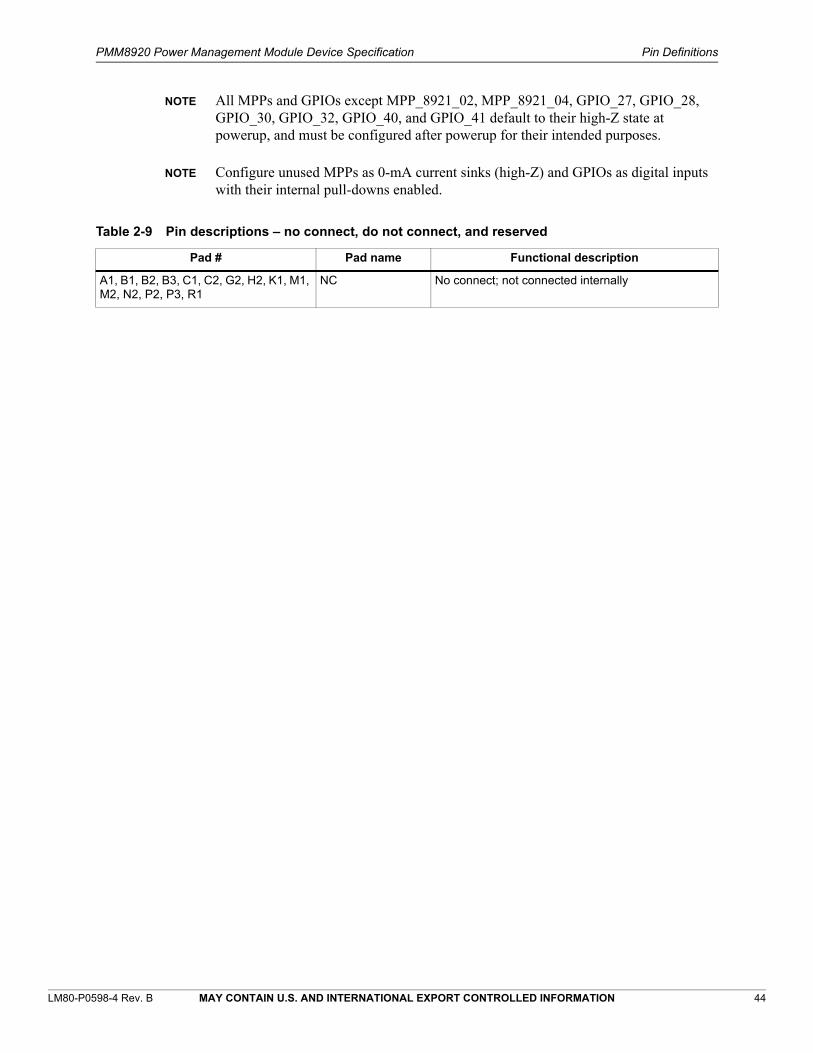
PMM8920 Power Management Module Device Specification Pin Definitions
LM80-P0598-4 Rev. B MAY CONTAIN U.S. AND INTERNATIONAL EXPORT CONTROLLED INFORMATION 44
NOTE All MPPs and GPIOs except MPP_8921_02, MPP_8921_04, GPIO_27, GPIO_28, GPIO_30, GPIO_32, GPIO_40, and GPIO_41 default to their high-Z state at powerup, and must be configured after powerup for their intended purposes.
NOTE Configure unused MPPs as 0-mA current sinks (high-Z) and GPIOs as digital inputs with their internal pull-downs enabled.
Table 2-9 Pin descriptions – no connect, do not connect, and reserved
Pad # Pad name Functional description
A1, B1, B2, B3, C1, C2, G2, H2, K1, M1, M2, N2, P2, P3, R1
NC No connect; not connected internally

PMM8920 Power Management Module Device Specification Pin Definitions
LM80-P0598-4 Rev. B MAY CONTAIN U.S. AND INTERNATIONAL EXPORT CONTROLLED INFORMATION 45
Table 2-10 Pin descriptions – input DC power
Pad # Pad name Functional description
D15, E17 USB_IN Power supply from USB charger to buck circuits.
D17 DC_IN Power supply from wall charger to buck circuits.
J17 VDD_CDRV Power supply for charger’s buck power FET driver.
E8 VDD_8921_L1_2_12_18 Power supply for PM8921 L1, L2, L12, and L18 LDO circuits; also powers digital interface pins to/from modem IC.
J3 VDD_8921_L3_15_17 Power supply for PM8921 L3, L15, and L17 LDO circuits.
G7 VDD_8921_L4_14 Power supply for PM8921 L4, L14, RF_CLK, and VREG_XO LDO circuits
G4 VDD_8921_L5_8_16 Power supply for PM8921 L5, L8, and L16 LDO circuits.
P1 VDD_8921_L6_7 Power supply for PM8921 L6 and L7 LDO circuits.
H6 VDD_8921_L9_11 Power supply for PM8921 L9 and L11 LDO circuits.
A7 VDD_8921_L10_22 Power supply for PM8921 L10 and L22 LDO circuits.
H3 VDD_8921_L21_23_29 Power supply for PM8921 L21, L23, and L29 LDO circuits.
E9 VDD_8921_L24 Power supply for PM8921 L24 LDO circuits.
C7 VDD_8921_L25 Power supply for PM8921 L25 LDO circuits.
M3 VDD_8921_L26 Power supply for PM8921 L26 LDO circuits.
L9 VDD_8921_L27 Power supply for PM8921 L27 LDO circuits.
N8 VDD_8921_L28 Power supply for PM8921 L28 LDO circuits.
B9 VDD_8921_S1 Power supply for PM8921 S1 buck converter.
A11 VDD_8921_S2 Power supply for PM8921 S2 buck converter.
C10 VDD_8921_S3 Power supply for PM8921 S3 buck converter.
R11 VDD_8921_S4 Power supply for PM8921 S4 buck converter.
A13, A14 VDD_8921_S5 Power supply for PM8921 S5 buck converter.
R13, R14 VDD_8921_S6 Power supply for PM8921 S6 buck converter.
P9 VDD_8921_S7 Power supply for PM8921 S7 buck converter.
R4, R5 VDD_8821_S1 Power supply for PM8821 S1 buck converter.
A4, A5 VDD_8821_S2 Power supply for PM8821 S1 buck converter.
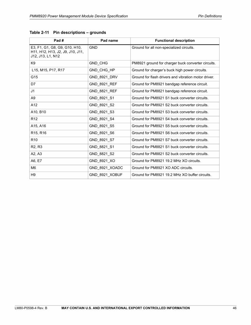
PMM8920 Power Management Module Device Specification Pin Definitions
LM80-P0598-4 Rev. B MAY CONTAIN U.S. AND INTERNATIONAL EXPORT CONTROLLED INFORMATION 46
Table 2-11 Pin descriptions – grounds
Pad # Pad name Functional description
E3, F1, G1, G8, G9, G10, H10, H11, H12, H13, J2, J9, J10, J11, J12, J13, L1, N12
GND Ground for all non-specialized circuits.
K9 GND_CHG PM8921 ground for charger buck converter circuits.
L15, M15, P17, R17 GND_CHG_HP Ground for charger’s buck high power circuits.
G15 GND_8921_DRV Ground for flash drivers and vibration motor driver.
D7 GND_8921_REF Ground for PM8921 bandgap reference circuit.
J1 GND_8821_REF Ground for PM8821 bandgap reference circuit.
A9 GND_8921_S1 Ground for PM8921 S1 buck converter circuits.
A12 GND_8921_S2 Ground for PM8921 S2 buck converter circuits.
A10, B10 GND_8921_S3 Ground for PM8921 S3 buck converter circuits.
R12 GND_8921_S4 Ground for PM8921 S4 buck converter circuits.
A15, A16 GND_8921_S5 Ground for PM8921 S5 buck converter circuits.
R15, R16 GND_8921_S6 Ground for PM8921 S6 buck converter circuits.
R10 GND_8921_S7 Ground for PM8921 S7 buck converter circuits.
R2, R3 GND_8821_S1 Ground for PM8821 S1 buck converter circuits.
A2, A3 GND_8821_S2 Ground for PM8821 S2 buck converter circuits.
A6, E7 GND_8921_XO Ground for PM8921 19.2 MHz XO circuits.
M6 GND_8921_XOADC Ground for PM8921 XO ADC circuits.
H9 GND_8921_XOBUF Ground for PM8921 19.2 MHz XO buffer circuits.

LM80-P0598-4 Rev. B MAY CONTAIN U.S. AND INTERNATIONAL EXPORT CONTROLLED INFORMATION 47
3 PMM8920 Electrical Specifications
3.1 Absolute maximum ratings
Operating the PMM8920 device under conditions beyond its absolute maximum ratings (Table 3-1) may damage the device. Absolute maximum ratings are limiting values to be considered individually when all other parameters are within their specified operating ranges. Operation and specification compliance under any absolute maximum condition, or after exposure to any of these conditions, is not guaranteed or implied. Exposure may affect device reliability.
Table 3-1 Absolute maximum ratings
Symbol Parameter Min Max Units
Power supply voltages 1
VOVP_SNS Voltage at the OVP sense pin (OVP_SNS) -2 +30 V
VDCIN External charger voltage (DCIN pins) -2 +12 V
VUSBIN External USB voltage (USB_IN pins) -2 +30
VDD Device power supply voltage (VPH_PWR and VDD_XX pins) -0.5 +6.0 V
VBAT_TRAN (< 10 ms)
Main battery voltage (VBAT pin) -0.5 +7.0 V
Signal pins 1
VLED_DRV Current driver (LED) output voltage -0.5 +6.0 V
VIN Voltage on any non-power supply pin 2 -0.5 VXX + 0.5 V
ESD protection and thermal conditions – see Section 9.1
1. Most operational pin voltages are limited by the device power supply voltage (VDD). Exceptions are listed below:• The over-voltage protection sense pin (OVP_SNS) is exposed to the full voltage from the external power supply
such as a wall charger, and the DC_IN pins are exposed to USB voltages or voltage-limited wall chargers.• The vibration motor driver output (VIB_DRV_N pin) is exposed to VDD plus the diode clamping voltage due to
inductive kickback from the motor. • The current driver outputs are capable of supporting +5 V operation.
2. VXX is the supply voltage associated with the input or output pin to which the test voltage is applied.

PMM8920 Power Management Module Device Specification PMM8920 Electrical Specifications
LM80-P0598-4 Rev. B MAY CONTAIN U.S. AND INTERNATIONAL EXPORT CONTROLLED INFORMATION 48
3.2 Recommended operating conditions
Operating conditions include parameters that are under the control of the user: power-supply voltage and ambient temperature, as listed in Table 3-2. The PMM8920 device meets all performance specifications listed within this chapter when used within the recommended operating conditions, unless otherwise noted within this chapter or those documents (provided the absolute maximum ratings have never been exceeded).
3.3 Performance specification details
Detailed electrical specifications for each die are available in the next two chapters. Chapter 4 has electrical specifications for PM8821 and Chapter 5 has electrical specifications for PM8921. Electrical specifications for the individual devices are still valid after integration into the module. Table 3-3 lists the performance specifications.
Table 3-2 Recommended operating conditions
Symbol Parameter Min Typ Max Units
Power supply voltages 1
VOVP Voltage at the over-voltage protection pin (USB_IN and OVP_SNS)
5.5 6.5 7 V
8.5 9.5 10 V
VDCIN External charger voltage (DCIN pins) 2 4.5 – 9.5 V
VUSBIN External USB voltage (USB_IN pins) 4.35 – 6.5 V
VDD Device power supply voltage (VPH_PWR and VDD_XX pins) 2.5 3 3.6 4.5 V
VBAT Main battery voltage (VBAT pin) 2.5 3 3.6 4.5 V
VCOIN Coin cell voltage (VCOIN pin) 2 3.0 3.25 V
VMSM_IO Digital I/O supply voltage 1.75 1.85 4 V
Signal pins 1
VLED_DRV Current driver (LED) output voltage 0.5 – +5.0 V
Thermal conditions
TC Operating temperature (case) -30 +25 +85 °C
1. Most operational pin voltages are limited by the device power supply voltage (VDD). Exceptions are listed below:• The over-voltage protection sense pin (OVP_SNS) is exposed to the full voltage from the external power supply
such as a wall charger, and the DC_IN pins are exposed to USB voltages or voltage-limited wall chargers.• The vibration motor driver output (VIB_DRV_N pin) is exposed to VDD plus the diode clamping voltage due to
inductive kickback from the motor. • The current driver outputs are capable of supporting +5 V operation.
2. The stated minimum value defines the threshold for the charger invalid interrupt only.3. Increased max to 4.5 V to support “High Voltage” Li batteries. Lower min to 2.5 V to support “Low Voltage” Li
batteries.4. Only 1.8 V I/O supported.

PMM8920 Power Management Module Device Specification PMM8920 Electrical Specifications
LM80-P0598-4 Rev. B MAY CONTAIN U.S. AND INTERNATIONAL EXPORT CONTROLLED INFORMATION 49
Table 3-3 Device specifications within PM8921 and PM8821 documents
FunctionPM8921 device specification
PM8821 device specification
DC power consumption X X
Digital logic characteristics X X
Input power management
Coin-cell charging
Battery voltage alarm
Undervoltage lockout
SMPL
X
X
X
X
–
–
–
–
Output power management
Voltage regulator and voltage switch summary
Voltage reference circuit
Buck switched-mode power supplies
Linear regulators 1
Voltage switches
1. PM8821 VDD_DIG is not pinned out in the PMM8920 device.
X
X
X
X
X
X
X
X
X
–
General housekeeping
Analog multiplexer and scaling circuits
HK/XO ADC circuits
19.2 MHz XO circuits
MP3 clock
32 kHz oscillator and sleep clock
19.2 MHz RC oscillator
Overtemperature protection
X
X
X
X
X
X
X
–
–
X
–
–
X
X
User interfaces
Light pulse generator
Current drivers
Vibration motor driver
External switch detections
Joystick support
User-programmable logic
X
X
X
X
X
X
–
–
–
–
–
–
IC-level interfaces
Poweron circuits and power sequences
Hardware configuration options and/or mode controls
SSBI and interrupt managers
UIM support
UART multiplexing
X
X
X
X
X
X
–
X
–
–
Configurable pins
GPIOs
MPPs
X
X
–
X
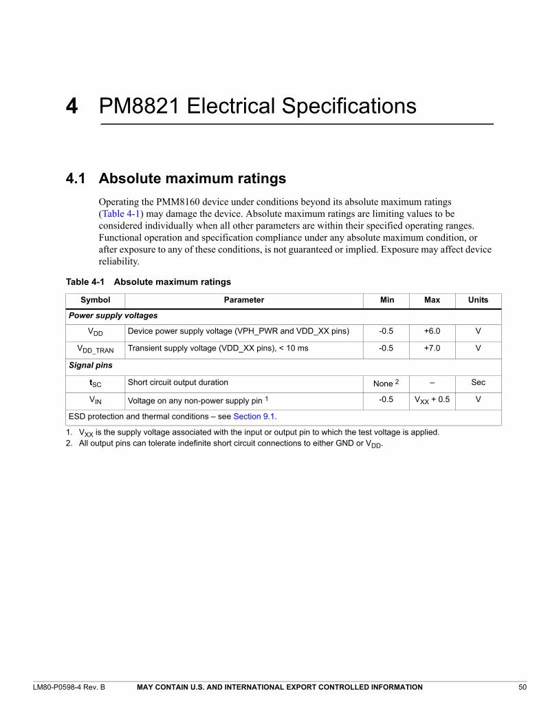
LM80-P0598-4 Rev. B MAY CONTAIN U.S. AND INTERNATIONAL EXPORT CONTROLLED INFORMATION 50
4 PM8821 Electrical Specifications
4.1 Absolute maximum ratings
Operating the PMM8160 device under conditions beyond its absolute maximum ratings (Table 4-1) may damage the device. Absolute maximum ratings are limiting values to be considered individually when all other parameters are within their specified operating ranges. Functional operation and specification compliance under any absolute maximum condition, or after exposure to any of these conditions, is not guaranteed or implied. Exposure may affect device reliability.
Table 4-1 Absolute maximum ratings
Symbol Parameter Min Max Units
Power supply voltages
VDD Device power supply voltage (VPH_PWR and VDD_XX pins) -0.5 +6.0 V
VDD_TRAN Transient supply voltage (VDD_XX pins), < 10 ms -0.5 +7.0 V
Signal pins
tSC Short circuit output duration None 2
2. All output pins can tolerate indefinite short circuit connections to either GND or VDD.
– Sec
VIN Voltage on any non-power supply pin 1
1. VXX is the supply voltage associated with the input or output pin to which the test voltage is applied.
-0.5 VXX + 0.5 V
ESD protection and thermal conditions – see Section 9.1.

PMM8920 Power Management Module Device Specification PM8821 Electrical Specifications
LM80-P0598-4 Rev. B MAY CONTAIN U.S. AND INTERNATIONAL EXPORT CONTROLLED INFORMATION 51
4.2 Recommended operating conditions
Operating conditions include parameters that are under the control of the user: power supply voltage and ambient temperature (Table 4-2). The PMM8160 device meets all performance specifications listed in Section 4.3 through Section 4.8 when used within the recommended operating conditions, unless otherwise noted in those sections (provided the absolute maximum ratings have never been exceeded).
Table 4-2 Recommended operating conditions
Symbol Parameter Min Typ Max Unit
Power supply voltages
VPH_PWR Device power supply voltage 2.5 3.6 4.5 V
VMSM_IO APQ-compatible digital I/O supply voltage 1.75 1.80 1.85 V
Signal pins
VIN Voltage on any non-power supply pin 1
1. VXX is the supply voltage associated with the input or output pin to which the test voltage is applied.
0 – VXX + 0.5 V
Thermal conditions
TC Operating temperature (case) -30 +25 +85 °C
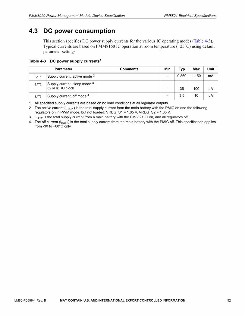
PMM8920 Power Management Module Device Specification PM8821 Electrical Specifications
LM80-P0598-4 Rev. B MAY CONTAIN U.S. AND INTERNATIONAL EXPORT CONTROLLED INFORMATION 52
4.3 DC power consumption
This section specifies DC power supply currents for the various IC operating modes (Table 4-3). Typical currents are based on PMM8160 IC operation at room temperature (+25°C) using default parameter settings.
Table 4-3 DC power supply currents1
1. All specified supply currents are based on no load conditions at all regulator outputs.
Parameter Comments Min Typ Max Unit
IBAT1 Supply current, active mode 2
2. The active current (IBAT1) is the total supply current from the main battery with the PMIC on and the following regulators on in PWM mode, but not loaded: VREG_S1 = 1.05 V, VREG_S2 = 1.05 V.
– 0.860 1.150 mA
IBAT2 Supply current, sleep mode 3 32 kHz RC clock
3. IBAT2 is the total supply current from a main battery with the PM8821 IC on, and all regulators off.
– 35 100 µA
IBAT3 Supply current, off mode 4
4. The off current (IBAT3) is the total supply current from the main battery with the PMIC off. This specification applies from -30 to +60°C only.
– 3.5 10 µA

PMM8920 Power Management Module Device Specification PM8821 Electrical Specifications
LM80-P0598-4 Rev. B MAY CONTAIN U.S. AND INTERNATIONAL EXPORT CONTROLLED INFORMATION 53
4.4 Digital logic characteristics
PMM8160 IC digital I/O characteristics such as voltage levels, current levels, and capacitance are specified in Table 4-4.
Table 4-4 Digital I/O characteristics 1
1. VIO is the supply voltage for the APQ/PM IC interface (most PMIC digital I/Os).
Parameter Comments Min Max Unit
VIH High-level input voltage 0.65·VIO VIO + 0.3 V
VIL Low-level input voltage -0.3 0.35·VIO V
VSHYS Schmitt hysteresis voltage 15 – mV
IL Input leakage current 2
2. MPP pins comply with the input leakage specification only when configured as a digital input or set to tri-state mode.
VIO = max, VIN = 0 V to VIO -0.20 +0.20 µA
VOH High-level output voltage Iout = IOH VIO - 0.45 VIO V
VOL Low-level output voltage Iout = IOL 0 0.45 V
IOH High-level output current 3
3. Output current specifications apply to all digital outputs unless specified otherwise, and are superseded by specifications for specific pins (such as MPP pins).
Vout = VOH 3 – mA
IOL Low-level output current 3 Vout = VOL – -3 mA
CIN Input capacitance 4
4. Input capacitance is guaranteed by design, but is not 100% tested.
– 5 pF

PMM8920 Power Management Module Device Specification PM8821 Electrical Specifications
LM80-P0598-4 Rev. B MAY CONTAIN U.S. AND INTERNATIONAL EXPORT CONTROLLED INFORMATION 54
4.5 Output power management
The PM8821 IC provides regulated voltages to supplement those generated by the PM8921 device. Three programmable voltage regulators are provided, and all are derived from a common bandgap reference circuit. Table 4-5 presents a high-level summary of all regulators and their intended uses.
Output voltage regulation circuits include:
Bandgap voltage reference circuit
Buck SMPS circuits
LDO linear regulator
All regulators can be set to a low power mode; as described in the following subsections.
Table 4-5 Voltage regulator summary
Type/name 1Default
conditions 3Used range 4
Low-power mode 5
Intended use
FT-SMPS – buck
S1 (2000 mA)
S2 (2000 mA)
Off, 1.050 V
Off, 1.050 V
0.500 to 1.350 V
0.500 to 1.350 V
PFM
PFM
Applications processor core #3
Applications processor core #4
Linear – 50 mA 2
VDD_DIG (PMOS) Off, 1.800 V 1.700 to 1.900 V LPM Internal PMIC Vdd
1. Each current listed in this table is its regulator's rated value – the current at which the regulator meets all its performance specifications. Higher currents are allowed, but higher input voltages may be required and some performance characteristics may become degraded. The pass transistor technology is included in this column with the PMOS linear regulator.
2. VDD_DIG is used as the Vdd source after power-up. Changing the programmed voltage or turning off VDD_DIG may have undesired consequences.
3. All regulators have default output voltage settings, even if they default to an off condition. 4. The used range includes all expected applications, plus limitations due to internal uses within the PMIC. See the
individual specification tables for the full programmable ranges.5. Indicates the type of low-power mode available. PFM = pulse frequency mode for SMPS, and LPM = low-power
bias mode for LDO regulators.

PMM8920 Power Management Module Device Specification PM8821 Electrical Specifications
LM80-P0598-4 Rev. B MAY CONTAIN U.S. AND INTERNATIONAL EXPORT CONTROLLED INFORMATION 55
4.5.1 Reference circuit
All PMIC regulator circuits and other internal circuits are driven by a common, on-chip voltage reference circuit. An on-chip series resistor supplements an off-chip 0.1 µF bypass capacitor at the REF_BYP pin to create a lowpass function that filters the reference voltage distributed throughout the device.
NOTE Do not load the REF_BYP pin. Use an MPP configured as an analog output if the reference voltage is needed off-chip.
Table 4-6 provides the applicable voltage reference performance specifications.
4.5.2 Buck switched-mode power supplies
The PM8821 buck converters are switched-mode power supplies with improved transient performance, enabling them to support applications processors that exhibit highly dynamic load conditions. The PMIC includes two fast-transient SMPS (FT-SMPS) circuits. Their normal operating mode is the fixed-frequency PWM, but they automatically switch to a frequency-varying PFM scheme for low-power operation. Table 4-7 list the buck converter performance specifications.
Table 4-6 Voltage reference performance specifications
Parameter Comments Min Typ Max Units
Nominal internal VREF At REF_BYP pin – 1.250 – V
Output voltage deviations
Normal operation
Normal operation
Sleep mode
Over temperature only, -20 to +120ºC
All operating conditions
All operating conditions
-0.32
-0.50
-1.00
–
–
–
+0.32
+0.50
+1.00
%
%
%
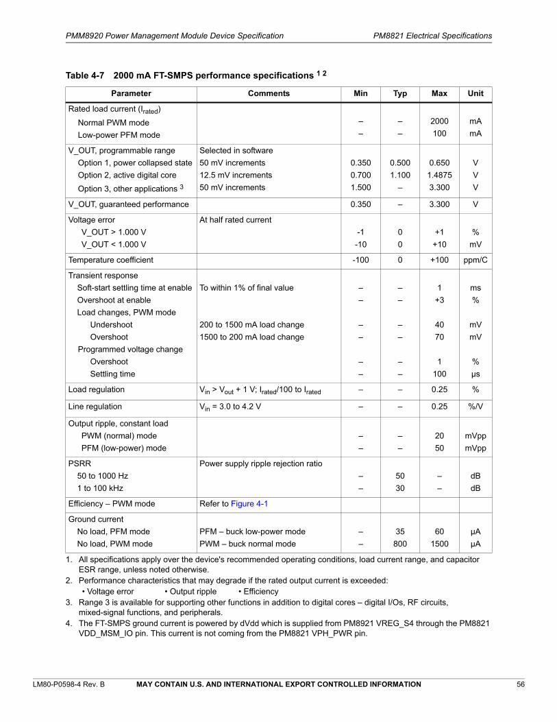
PMM8920 Power Management Module Device Specification PM8821 Electrical Specifications
LM80-P0598-4 Rev. B MAY CONTAIN U.S. AND INTERNATIONAL EXPORT CONTROLLED INFORMATION 56
Table 4-7 2000 mA FT-SMPS performance specifications 1 2
Parameter Comments Min Typ Max Unit
Rated load current (Irated)
Normal PWM mode
Low-power PFM mode
–
–
–
–
2000
100
mA
mA
V_OUT, programmable range
Option 1, power collapsed state
Option 2, active digital core
Option 3, other applications 3
Selected in software
50 mV increments
12.5 mV increments
50 mV increments
0.350
0.700
1.500
0.500
1.100
–
0.650
1.4875
3.300
V
V
V
V_OUT, guaranteed performance 0.350 – 3.300 V
Voltage error
V_OUT > 1.000 V
V_OUT < 1.000 V
At half rated current
-1
-10
0
0
+1
+10
%
mV
Temperature coefficient -100 0 +100 ppm/C
Transient response
Soft-start settling time at enable
Overshoot at enable
Load changes, PWM mode
Undershoot
Overshoot
Programmed voltage change
Overshoot
Settling time
To within 1% of final value
200 to 1500 mA load change
1500 to 200 mA load change
–
–
–
–
–
–
–
–
–
–
–
–
1
+3
40
70
1
100
ms
%
mV
mV
%
µs
Load regulation Vin > Vout + 1 V; Irated/100 to Irated – – 0.25 %
Line regulation Vin = 3.0 to 4.2 V – – 0.25 %/V
Output ripple, constant load
PWM (normal) mode
PFM (low-power) mode
–
–
–
–
20
50
mVpp
mVpp
PSRR
50 to 1000 Hz
1 to 100 kHz
Power supply ripple rejection ratio
–
–
50
30
–
–
dB
dB
Efficiency – PWM mode Refer to Figure 4-1
Ground current
No load, PFM mode
No load, PWM mode
PFM – buck low-power mode
PWM – buck normal mode
–
–
35
800
60
1500
µA
µA
1. All specifications apply over the device's recommended operating conditions, load current range, and capacitor ESR range, unless noted otherwise.
2. Performance characteristics that may degrade if the rated output current is exceeded:• Voltage error • Output ripple • Efficiency
3. Range 3 is available for supporting other functions in addition to digital cores – digital I/Os, RF circuits, mixed-signal functions, and peripherals.
4. The FT-SMPS ground current is powered by dVdd which is supplied from PM8921 VREG_S4 through the PM8821 VDD_MSM_IO pin. This current is not coming from the PM8821 VPH_PWR pin.
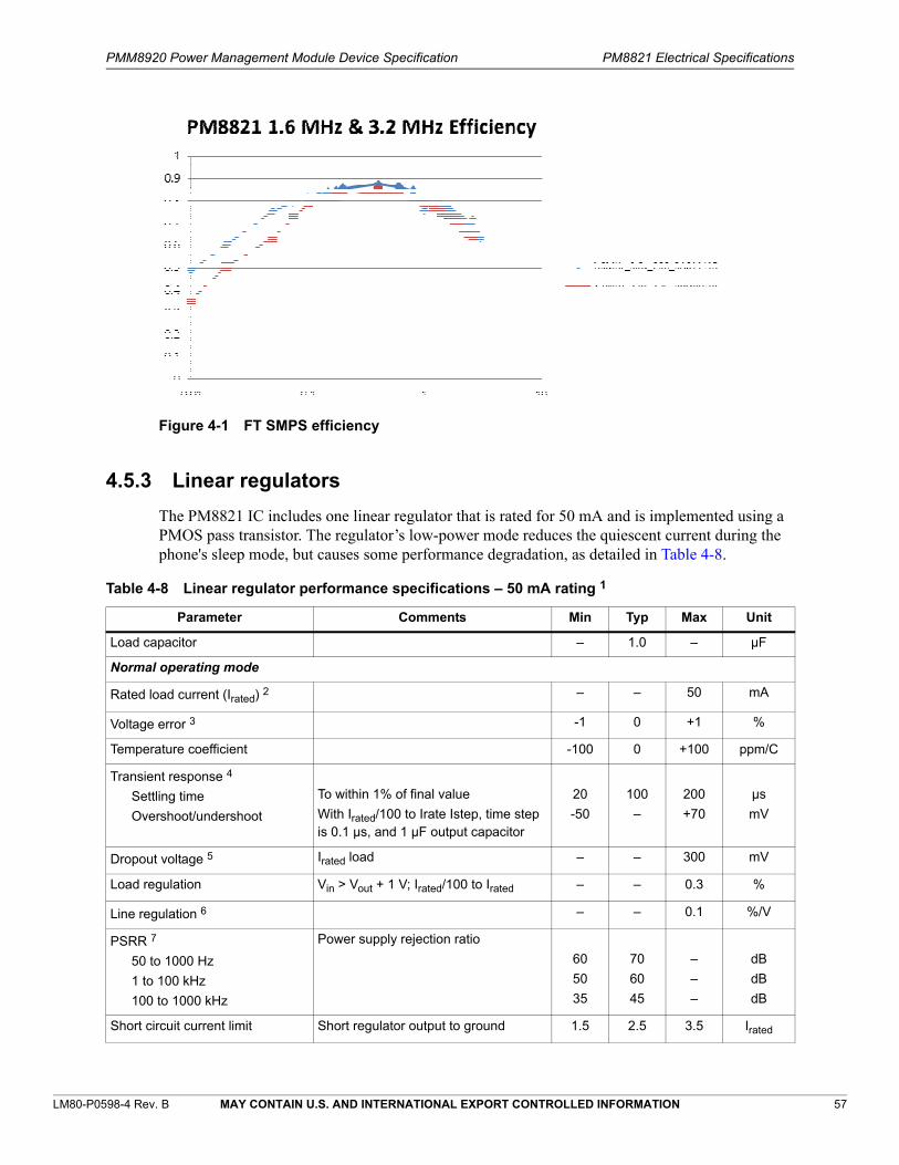
PMM8920 Power Management Module Device Specification PM8821 Electrical Specifications
LM80-P0598-4 Rev. B MAY CONTAIN U.S. AND INTERNATIONAL EXPORT CONTROLLED INFORMATION 57
Figure 4-1 FT SMPS efficiency
4.5.3 Linear regulators
The PM8821 IC includes one linear regulator that is rated for 50 mA and is implemented using a PMOS pass transistor. The regulator’s low-power mode reduces the quiescent current during the phone's sleep mode, but causes some performance degradation, as detailed in Table 4-8.
Table 4-8 Linear regulator performance specifications – 50 mA rating 1
Parameter Comments Min Typ Max Unit
Load capacitor – 1.0 – µF
Normal operating mode
Rated load current (Irated) 2 – – 50 mA
Voltage error 3 -1 0 +1 %
Temperature coefficient -100 0 +100 ppm/C
Transient response 4
Settling time
Overshoot/undershoot
To within 1% of final value
With Irated/100 to Irate Istep, time step is 0.1 μs, and 1 μF output capacitor
20
-50
100
–
200
+70
µs
mV
Dropout voltage 5 Irated load – – 300 mV
Load regulation Vin > Vout + 1 V; Irated/100 to Irated – – 0.3 %
Line regulation 6 – – 0.1 %/V
PSRR 7
50 to 1000 Hz
1 to 100 kHz
100 to 1000 kHz
Power supply rejection ratio
60
50
35
70
60
45
–
–
–
dB
dB
dB
Short circuit current limit Short regulator output to ground 1.5 2.5 3.5 Irated
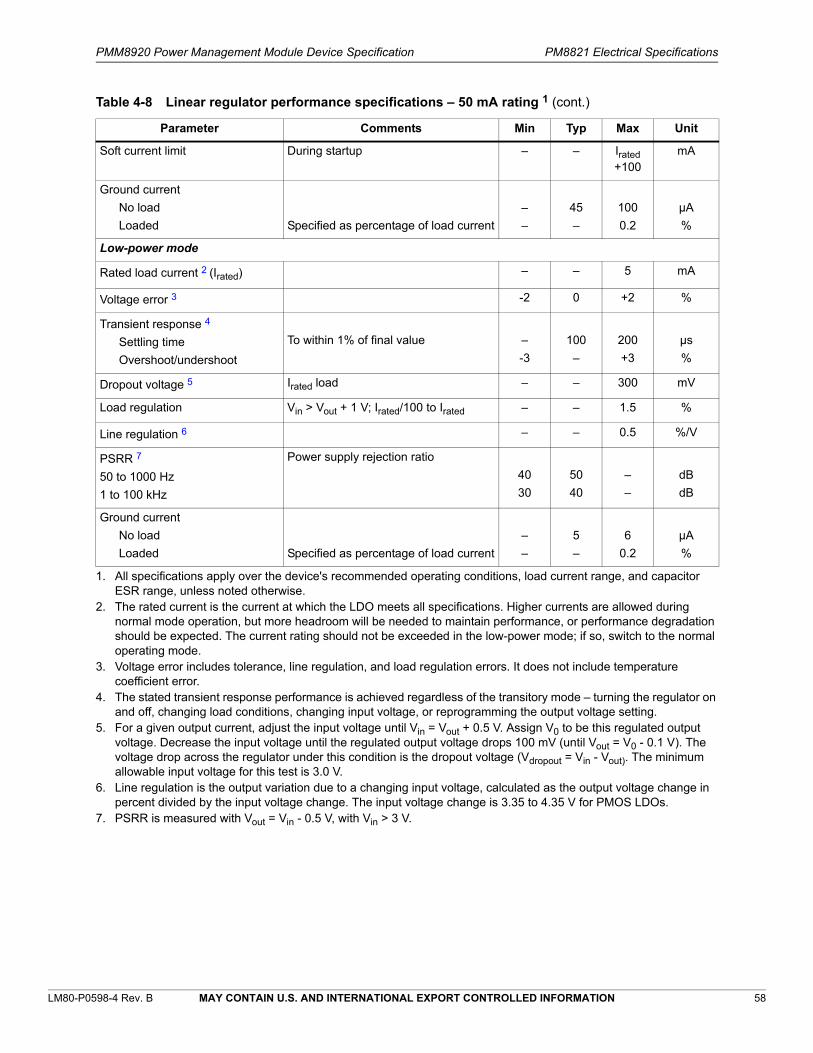
PMM8920 Power Management Module Device Specification PM8821 Electrical Specifications
LM80-P0598-4 Rev. B MAY CONTAIN U.S. AND INTERNATIONAL EXPORT CONTROLLED INFORMATION 58
Soft current limit During startup – – Irated +100
mA
Ground current
No load
Loaded Specified as percentage of load current
–
–
45
–
100
0.2
µA
%
Low-power mode
Rated load current 2 (Irated) – – 5 mA
Voltage error 3 -2 0 +2 %
Transient response 4
Settling time
Overshoot/undershoot
To within 1% of final value –
-3
100
–
200
+3
µs
%
Dropout voltage 5 Irated load – – 300 mV
Load regulation Vin > Vout + 1 V; Irated/100 to Irated – – 1.5 %
Line regulation 6 – – 0.5 %/V
PSRR 7
50 to 1000 Hz
1 to 100 kHz
Power supply rejection ratio
40
30
50
40
–
–
dB
dB
Ground current
No load
Loaded Specified as percentage of load current
–
–
5
–
6
0.2
µA
%
1. All specifications apply over the device's recommended operating conditions, load current range, and capacitor ESR range, unless noted otherwise.
2. The rated current is the current at which the LDO meets all specifications. Higher currents are allowed during normal mode operation, but more headroom will be needed to maintain performance, or performance degradation should be expected. The current rating should not be exceeded in the low-power mode; if so, switch to the normal operating mode.
3. Voltage error includes tolerance, line regulation, and load regulation errors. It does not include temperature coefficient error.
4. The stated transient response performance is achieved regardless of the transitory mode – turning the regulator on and off, changing load conditions, changing input voltage, or reprogramming the output voltage setting.
5. For a given output current, adjust the input voltage until Vin = Vout + 0.5 V. Assign V0 to be this regulated output voltage. Decrease the input voltage until the regulated output voltage drops 100 mV (until Vout = V0 - 0.1 V). The voltage drop across the regulator under this condition is the dropout voltage (Vdropout = Vin - Vout). The minimum allowable input voltage for this test is 3.0 V.
6. Line regulation is the output variation due to a changing input voltage, calculated as the output voltage change in percent divided by the input voltage change. The input voltage change is 3.35 to 4.35 V for PMOS LDOs.
7. PSRR is measured with Vout = Vin - 0.5 V, with Vin > 3 V.
Table 4-8 Linear regulator performance specifications – 50 mA rating 1 (cont.)
Parameter Comments Min Typ Max Unit
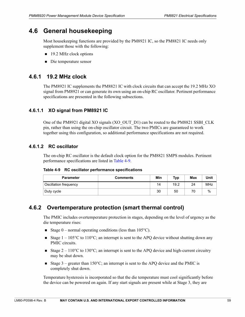
PMM8920 Power Management Module Device Specification PM8821 Electrical Specifications
LM80-P0598-4 Rev. B MAY CONTAIN U.S. AND INTERNATIONAL EXPORT CONTROLLED INFORMATION 59
4.6 General housekeeping
Most housekeeping functions are provided by the PM8921 IC, so the PM8821 IC needs only supplement those with the following:
19.2 MHz clock options
Die temperature sensor
4.6.1 19.2 MHz clock
The PM8921 IC supplements the PM8821 IC with clock circuits that can accept the 19.2 MHz XO signal from PM8921 or can generate its own using an on-chip RC oscillator. Pertinent performance specifications are presented in the following subsections.
4.6.1.1 XO signal from PM8921 IC
One of the PM8921 digital XO signals (XO_OUT_D1) can be routed to the PM8821 SSBI_CLK pin, rather than using the on-chip oscillator circuit. The two PMICs are guaranteed to work together using this configuration, so additional performance specifications are not required.
4.6.1.2 RC oscillator
The on-chip RC oscillator is the default clock option for the PM8821 SMPS modules. Pertinent performance specifications are listed in Table 4-9.
4.6.2 Overtemperature protection (smart thermal control)
The PMIC includes overtemperature protection in stages, depending on the level of urgency as the die temperature rises:
Stage 0 – normal operating conditions (less than 105°C).
Stage 1 – 105°C to 110°C; an interrupt is sent to the APQ device without shutting down any PMIC circuits.
Stage 2 – 110°C to 130°C; an interrupt is sent to the APQ device and high-current circuitry may be shut down.
Stage 3 – greater than 150°C; an interrupt is sent to the APQ device and the PMIC is completely shut down.
Temperature hysteresis is incorporated so that the die temperature must cool significantly before the device can be powered on again. If any start signals are present while at Stage 3, they are
Table 4-9 RC oscillator performance specifications
Parameter Comments Min Typ Max Unit
Oscillation frequency 14 19.2 24 MHz
Duty cycle 30 50 70 %

PMM8920 Power Management Module Device Specification PM8821 Electrical Specifications
LM80-P0598-4 Rev. B MAY CONTAIN U.S. AND INTERNATIONAL EXPORT CONTROLLED INFORMATION 60
ignored until Stage 0 is reached. When the device cools enough to reach Stage 0 and a start signal is present, the PMIC will power up immediately.
4.7 User interfaces
The PM8821 IC does not include any circuits that are dedicated to user interface functions, but the MPPs can be configured to enable such features. General MPP performance is specified in the following section, followed by additional discussion of the configurations that support user interface features.
4.7.1 MPP pin specifications
The PM8821 IC includes four MPPs that can be configured for any function specified within Table 4-10.
Table 4-10 Multipurpose pin performance specifications
Parameter Comments Min Typ Max Unit
MPP configured as digital input 1
1. VYY1 is the programmable supply voltage from which digital input thresholds are referenced; options are listed in Table 2-1. Other specifications are included in Table 4-4.
Logic high input voltage 0.65·VYY1 – – V
Logic low input voltage – – 0.35·VYY1 V
MPP configured as digital output 2
2. VYY2 is the programmable supply voltage from which digital output thresholds are referenced; options are listed in Table 2-1. Other specifications are included in Table 4-4. The input and output supply voltages can be different.
Logic high output voltage Iout = IOH VYY2 - 0.45 – VYY2 V
Logic low output voltage Iout = IOL 0 – 0.45 V
MPP configured as bidirectional I/O 3
3. MPP pairs are listed in Table 4-11.
Nominal pull-up resistance Programmable range 4
4. Pull-up resistance is programmable to values of 1 k, 10 k, 30 k, or open; if used, tolerance is ±20%.
1 – 30 k
Maximum frequency 4 – – MHz
Switch on resistance – 20 50
Power supply current – 6 7 µA
MPP configured as analog output (buffered VREF output)
Output voltage error -50 µA to +50 µA – – 12.5 mV
Temperature variation Due to buffer only; does not include VREF variation (see Table 4-6).
-0.03 – +0.03 %
Load capacitance – – 25 pF
Power supply current – 0.17 0.20 mA
MPP configured as current driver output (see Section 4.7.2)

PMM8920 Power Management Module Device Specification PM8821 Electrical Specifications
LM80-P0598-4 Rev. B MAY CONTAIN U.S. AND INTERNATIONAL EXPORT CONTROLLED INFORMATION 61
4.7.2 Digital control output
MPP performance specifications for these uses are listed in Section 4.7.1.
4.8 IC-level interfaces
The IC-level interfaces include poweron circuits; the SSBI; and an interrupt manager and its outputs. All parameters associated with these IC-level interface functions are specified in the following subsections. MPP functions can also be used as an IC-level interface, but they are specified in Section 4.7.1.
4.8.1 Poweron circuits and the power sequences
PM8821 power sequences are initiated when the PM8921 device drives PON_RESET_N high.
The PM8821 PON_RESET_N signal is not used since the PM8921 device will assert PON_RESET_N high to both the PM8821 device and the APQ/MPQ simultaneously. The PM8821 does not have any default-on regulators except for VDD_DIG, which is only used internally for PM8821. Therefore, there is no defined poweron sequence for the PM8821 device.
4.8.2 SSBI and the interrupt manager
The SSBI is a bidirectional digital signal that is used for all primary communications between the PM and APQ devices. The SSBI clock can either use the SSBI_CLK that comes from the PM8921 IC (XO_OUT_D1) or the ALT_SSBI_CLK from the APQ device. Both of these signals meet the voltage and current level requirements stated in Table 4-4.
The interrupt manager reports on numerous conditions, conveying realtime and latched status signals to the APQ device, thereby supporting its interrupt processing. The PM8821 IC uses a single interrupt line. The interrupt manager is a mostly embedded function; the interrupt output signal meet the voltage and current level requirements stated in Table 4-4.
Table 4-11 MPP pairs
MPP # Pin # MPP # Pin #
1 30 – 2 24
3 18 – 4 17

LM80-P0598-4 Rev. B MAY CONTAIN U.S. AND INTERNATIONAL EXPORT CONTROLLED INFORMATION 62
5 PM8921 Electrical Specifications
5.1 Absolute maximum ratings
Operating the PMM8160 device under conditions beyond its absolute maximum ratings (Table 5-1) may damage the device. Absolute maximum ratings are limiting values to be considered individually when all other parameters are within their specified operating ranges. Functional operation and specification compliance under any absolute maximum condition, or after exposure to any of these conditions, is not guaranteed or implied. Exposure may affect device reliability.
Table 5-1 Absolute maximum ratings
Symbol Parameter Min Max Units
Power supply voltages11
VOVP_SNS Voltage at the OVP sense pin (OVP_SNS) -2 +30 V
VDCIN External charger voltage (DCIN pins) -2 +12 V
VUSBIN External USB voltage (USB_IN pins) -2 +30 V
VDD Device power supply voltage (VPH_PWR and VDD_XX pins) -0.5 +6.0 V
VBAT_TRAN (< 10 ms) Main battery voltage (VBAT pin) -0.5 +7.0 V
Signal pins 1
VLED_DRV Current driver (LED) output voltage -0.5 +6.0 V
VIN Voltage on any non-power supply pin22 -0.5 VXX + 0.5 V
ESD protection and thermal conditions – see Section 7.1
1. Most operational pin voltages are limited by the device power supply voltage (VDD). Exceptions are listed below:• The over-voltage protection sense pin (OVP_SNS) is exposed to the full voltage from the external power supply
such as a wall charger, and the DC_IN pins are exposed to USB voltages or voltage-limited wall chargers.• The vibration motor driver output (VIB_DRV_N pin) is exposed to VDD plus the diode clamping voltage due to
inductive kickback from the motor. • The current driver outputs are capable of supporting +5 V operation.
2. VXX is the supply voltage associated with the input or output pin to which the test voltage is applied.

PMM8920 Power Management Module Device Specification PM8921 Electrical Specifications
LM80-P0598-4 Rev. B MAY CONTAIN U.S. AND INTERNATIONAL EXPORT CONTROLLED INFORMATION 63
5.2 Recommended operating conditions
Operating conditions include parameters that are under the control of the user: power supply voltage and ambient temperature (Table 5-2). The PMM8160 device meets all performance specifications listed in Section 5.3 through Section 5.11 when used within the recommended operating conditions unless otherwise noted in those sections (provided the absolute maximum ratings have never been exceeded).
Table 5-2 Recommended operating conditions
Symbol Parameter Min Typ Max Units
Power supply voltages11
1. Most operational pin voltages are limited by the device power supply voltage (VDD). Exceptions are listed below:•The over-voltage protection sense pin (OVP_SNS) is exposed to the full voltage from the external power supply
such as a wall charger, and the DC_IN pins are exposed to USB voltages or voltage-limited wall chargers.•The vibration motor driver output (VIB_DRV_N pin) is exposed to VDD plus the diode clamping voltage due to
inductive kickback from the motor. • The current driver outputs are capable of supporting +5 V operation.
VOVP Voltage at the over-voltage protection pin
USB_IN
OVP_SNS
3.3
3.3
–
–
28
28
V
V
VDCIN External charger voltage (DCIN pins)22
2. The stated minimum value defines the threshold for the charger invalid interrupt only.
4.35 – 9.5 V
VDD Device power supply voltage (VPH_PWR and VDD_XX pins)33
3. Increased maximum to 4.5 V to support “high-voltage” Li batteries. Lower min to 2.5 V to support “low-voltage” Li batteries.
2.5 3.6 4.5 V
VBAT Main battery voltage (VBAT pin) 3 2.5 3.6 4.5 V
VCOIN Coincell voltage (VCOIN pin) 2 3.0 3.25 V
VMSM_IO Digital I/O supply voltage44
4. Only 1.8 V I/O supported.
1.75 – 1.85 V
Signal pins 1
VLED_DRV Current driver (LED) output voltage 0.5 – +5.0 V
Thermal conditions
TC Operating temperature (case) -30 +25 +85 °C

PMM8920 Power Management Module Device Specification PM8921 Electrical Specifications
LM80-P0598-4 Rev. B MAY CONTAIN U.S. AND INTERNATIONAL EXPORT CONTROLLED INFORMATION 64
5.3 DC power consumption
This section specifies DC power supply currents for the various IC operating modes (Table 5-3). Typical currents are based upon PMM8160 IC operation at room temperature (+25°C) using default parameter settings.
Table 5-3 DC power supply currents
Parameter Comments Min Typ Max Unit
IBAT1 Supply current, active mode11
1. IBAT1 is the total supply current from a main battery with the PM8921 IC on, crystal oscillators on, XO_D0 on at 19.2 MHz, driving no load, and these voltage regulators on with no load at the following: VREG_S1 = 1.225 V, VREG_S3 = 1.05 V, VREG_S4 = 1.8 V, VREG_L1 = 1.05 V, VREG_L3 = 3.075 V, VREG_L4 = 1.8 V, VREG_L5 = 2.95 V, VREG_L6 = 2.95 V, VREG_L7 = 2.95 V, VREG_L24 = 1.05 V, VREG_L25 = 1.225 V (bypass mode), and MPP5 = 1.25 V.
– 5.3 6.0 mA
IBAT2 Supply current, sleep mode22
32 kHz XTAL clock
19.2 MHz XO clock
2. IBAT2 is the total supply current from a main battery with the PM8921 IC on, these voltage regulators on with no load and low-power mode enabled: VREG_S1 = 0.75 V, VREG_S3 = 0.75 V, VREG_S4 = 1.8 V, VREG_L1 = 1.05 V, VREG_L4 = 1.8 V, VREG_L5 = 2.95 V, VREG_L6 = 2.95 V, VREG_L24 = 0.75 V (bypass mode), VREG_L25 = 0.75 V (bypass mode). All other regulators are off, 19.2 MHz crystal oscillator is off, XO buffer off, and all XO_EN signals are low. MBG is in low-power mode.
–
–
160
240
240
360
µA
µA
IBAT3 Supply current, off mode33
3. IBAT3 is the total supply current from a main battery with the PM8921 IC off and the 32 kHz crystal oscillator on. This only applies when the temperature is between -30°C and 60°C.
– 5 18 µA
ICOIN Coincell supply current 44
Off mode, XTAL on
Off mode, XTAL off
Off mode, RCCAL55
4. ICOIN is the total supply current from a 3.0 V coin cell with the PM8921 IC off and the 32 kHz crystal oscillator on. This only applies when the temperature is between -30°C and 60°C.
5. This is the total supply current from a 3.0 V coin cell with the PM8921 device off, the 32 kHz crystal oscillator off, and cal RC enabled with nominal settings. This is the average current, and only applies when the temperature is between -20°C and 60°C.
–
–
–
2.5
2
5
3
2.5
8
µA
µA
µA
ICHG External supply current 66
6. ICHG is the total supply current from a charger, with the device configured into the sleep mode as specified in Note 2 above with DC_IN = 7.0 V and VMAXSEL setting = 4.2 V.
Sleep mode – 13.3 15.0 mA
IUSB USB charger supply current Suspend mode – – 1.65 mA
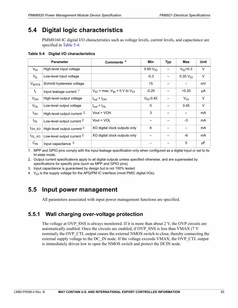
PMM8920 Power Management Module Device Specification PM8921 Electrical Specifications
LM80-P0598-4 Rev. B MAY CONTAIN U.S. AND INTERNATIONAL EXPORT CONTROLLED INFORMATION 65
5.4 Digital logic characteristics
PMM8160 IC digital I/O characteristics such as voltage levels, current levels, and capacitance are specified in Table 5-4.
5.5 Input power management
All parameters associated with input power management functions are specified.
5.5.1 Wall charging over-voltage protection
The voltage at OVP_SNS is always monitored. If it is more than about 2 V, the OVP circuits are automatically enabled. Once the circuits are enabled, if OVP_SNS is less than VMAX (7 V nominal), the OVP_CTL output causes the external NMOS switch to close, thereby connecting the external supply voltage to the DC_IN node. If the voltage exceeds VMAX, the OVP_CTL output is immediately driven low to open the NMOS switch and protect the DCIN node.
Table 5-4 Digital I/O characteristics
Parameter Comments44
4. VIO is the supply voltage for the APQ/PM IC interface (most PMIC digital I/Os).
Min Typ Max Unit
VIH High-level input voltage 0.65·VIO – VIO+0.3 V
VIL Low-level input voltage -0.3 – 0.35·VIO V
VSHYS Schmitt hysteresis voltage 15 – – mV
IL Input leakage current11
1. MPP and GPIO pins comply with the input leakage specification only when configured as a digital input or set to its tri-state mode.
VIO = max, VIN = 0 V to VIO -0.20 – +0.20 µA
VOH High-level output voltage Iout = IOH VIO-0.45 – VIO V
VOL Low-level output voltage Iout = IOL 0 – 0.45 V
IOH High-level output current22
2. Output current specifications apply to all digital outputs unless specified otherwise, and are superseded by specifications for specific pins (such as MPP and GPIO pins).
Vout = VOH 3 – – mA
IOL Low-level output current 2 Vout = VOL – – -3 mA
IOH_XO High-level output current 2 XO digital clock outputs only 6 – – mA
IOL_XO Low-level output current 2 XO digital clock outputs only – – -6 mA
CIN Input capacitance33
3. Input capacitance is guaranteed by design but is not 100% tested.
– – 5 pF
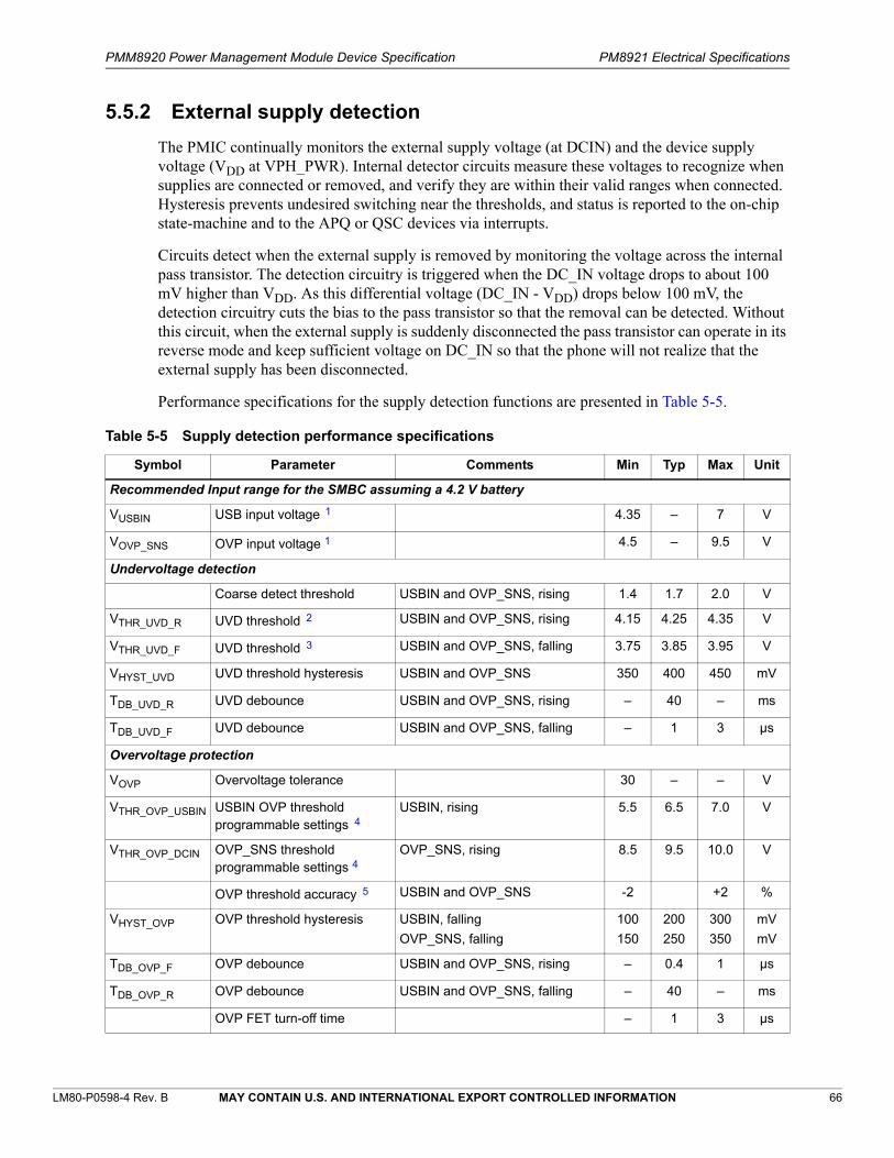
PMM8920 Power Management Module Device Specification PM8921 Electrical Specifications
LM80-P0598-4 Rev. B MAY CONTAIN U.S. AND INTERNATIONAL EXPORT CONTROLLED INFORMATION 66
5.5.2 External supply detection
The PMIC continually monitors the external supply voltage (at DCIN) and the device supply voltage (VDD at VPH_PWR). Internal detector circuits measure these voltages to recognize when supplies are connected or removed, and verify they are within their valid ranges when connected. Hysteresis prevents undesired switching near the thresholds, and status is reported to the on-chip state-machine and to the APQ or QSC devices via interrupts.
Circuits detect when the external supply is removed by monitoring the voltage across the internal pass transistor. The detection circuitry is triggered when the DC_IN voltage drops to about 100 mV higher than VDD. As this differential voltage (DC_IN - VDD) drops below 100 mV, the detection circuitry cuts the bias to the pass transistor so that the removal can be detected. Without this circuit, when the external supply is suddenly disconnected the pass transistor can operate in its reverse mode and keep sufficient voltage on DC_IN so that the phone will not realize that the external supply has been disconnected.
Performance specifications for the supply detection functions are presented in Table 5-5.
Table 5-5 Supply detection performance specifications
Symbol Parameter Comments Min Typ Max Unit
Recommended Input range for the SMBC assuming a 4.2 V battery
VUSBIN USB input voltage11 4.35 – 7 V
VOVP_SNS OVP input voltage 1 4.5 – 9.5 V
Undervoltage detection
Coarse detect threshold USBIN and OVP_SNS, rising 1.4 1.7 2.0 V
VTHR_UVD_R UVD threshold22 USBIN and OVP_SNS, rising 4.15 4.25 4.35 V
VTHR_UVD_F UVD threshold33 USBIN and OVP_SNS, falling 3.75 3.85 3.95 V
VHYST_UVD UVD threshold hysteresis USBIN and OVP_SNS 350 400 450 mV
TDB_UVD_R UVD debounce USBIN and OVP_SNS, rising – 40 – ms
TDB_UVD_F UVD debounce USBIN and OVP_SNS, falling – 1 3 µs
Overvoltage protection
VOVP Overvoltage tolerance 30 – – V
VTHR_OVP_USBIN USBIN OVP threshold programmable settings44
USBIN, rising 5.5 6.5 7.0 V
VTHR_OVP_DCIN OVP_SNS threshold programmable settings 4
OVP_SNS, rising 8.5 9.5 10.0 V
OVP threshold accuracy55 USBIN and OVP_SNS -2 +2 %
VHYST_OVP OVP threshold hysteresis USBIN, falling
OVP_SNS, falling
100
150
200
250
300
350
mV
mV
TDB_OVP_F OVP debounce USBIN and OVP_SNS, rising – 0.4 1 µs
TDB_OVP_R OVP debounce USBIN and OVP_SNS, falling – 40 – ms
OVP FET turn-off time – 1 3 µs
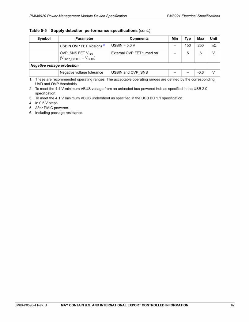
PMM8920 Power Management Module Device Specification PM8921 Electrical Specifications
LM80-P0598-4 Rev. B MAY CONTAIN U.S. AND INTERNATIONAL EXPORT CONTROLLED INFORMATION 67
USBIN OVP FET Rds(on)66 USBIN = 5.0 V – 150 250 mΩ
OVP_SNS FET VGS (VOVP_CNTRL – VCHG)
External OVP FET turned on – 5 6 V
Negative voltage protection
Negative voltage tolerance USBIN and OVP_SNS – – -0.3 V
1. These are recommended operating ranges. The acceptable operating ranges are defined by the corresponding UVD and OVP thresholds.
2. To meet the 4.4 V minimum VBUS voltage from an unloaded bus-powered hub as specified in the USB 2.0 specification.
3. To meet the 4.1 V minimum VBUS undershoot as specified in the USB BC 1.1 specification.4. In 0.5 V steps.5. After PMIC poweron.6. Including package resistance.
Table 5-5 Supply detection performance specifications (cont.)
Symbol Parameter Comments Min Typ Max Unit
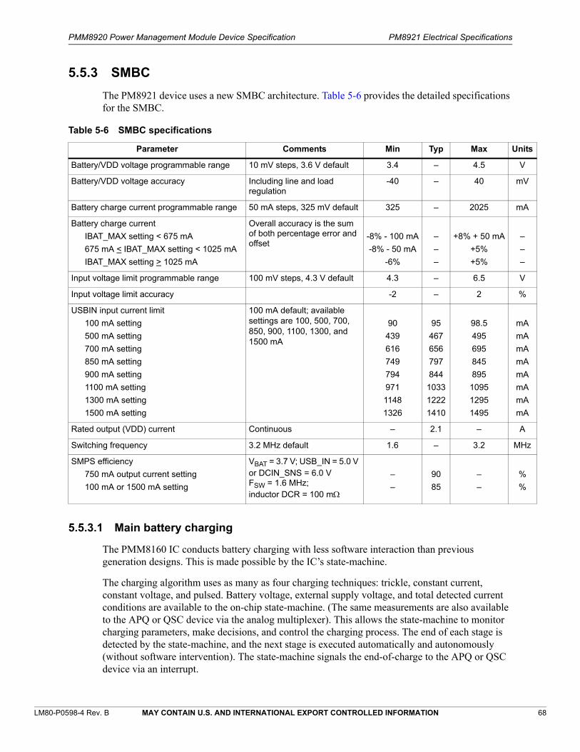
PMM8920 Power Management Module Device Specification PM8921 Electrical Specifications
LM80-P0598-4 Rev. B MAY CONTAIN U.S. AND INTERNATIONAL EXPORT CONTROLLED INFORMATION 68
5.5.3 SMBC
The PM8921 device uses a new SMBC architecture. Table 5-6 provides the detailed specifications for the SMBC.
5.5.3.1 Main battery charging
The PMM8160 IC conducts battery charging with less software interaction than previous generation designs. This is made possible by the IC’s state-machine.
The charging algorithm uses as many as four charging techniques: trickle, constant current, constant voltage, and pulsed. Battery voltage, external supply voltage, and total detected current conditions are available to the on-chip state-machine. (The same measurements are also available to the APQ or QSC device via the analog multiplexer). This allows the state-machine to monitor charging parameters, make decisions, and control the charging process. The end of each stage is detected by the state-machine, and the next stage is executed automatically and autonomously (without software intervention). The state-machine signals the end-of-charge to the APQ or QSC device via an interrupt.
Table 5-6 SMBC specifications
Parameter Comments Min Typ Max Units
Battery/VDD voltage programmable range 10 mV steps, 3.6 V default 3.4 – 4.5 V
Battery/VDD voltage accuracy Including line and load regulation
-40 – 40 mV
Battery charge current programmable range 50 mA steps, 325 mV default 325 – 2025 mA
Battery charge current
IBAT_MAX setting < 675 mA
675 mA < IBAT_MAX setting < 1025 mA
IBAT_MAX setting > 1025 mA
Overall accuracy is the sum of both percentage error and offset
-8% - 100 mA
-8% - 50 mA
-6%
–
–
–
+8% + 50 mA
+5%
+5%
–
–
–
Input voltage limit programmable range 100 mV steps, 4.3 V default 4.3 – 6.5 V
Input voltage limit accuracy -2 – 2 %
USBIN input current limit
100 mA setting
500 mA setting
700 mA setting
850 mA setting
900 mA setting
1100 mA setting
1300 mA setting
1500 mA setting
100 mA default; available settings are 100, 500, 700, 850, 900, 1100, 1300, and 1500 mA
90
439
616
749
794
971
1148
1326
95
467
656
797
844
1033
1222
1410
98.5
495
695
845
895
1095
1295
1495
mA
mA
mA
mA
mA
mA
mA
mA
Rated output (VDD) current Continuous – 2.1 – A
Switching frequency 3.2 MHz default 1.6 – 3.2 MHz
SMPS efficiency
750 mA output current setting
100 mA or 1500 mA setting
VBAT = 3.7 V; USB_IN = 5.0 V or DCIN_SNS = 6.0 VFSW = 1.6 MHz;inductor DCR = 100 m
–
–
90
85
–
–
%
%
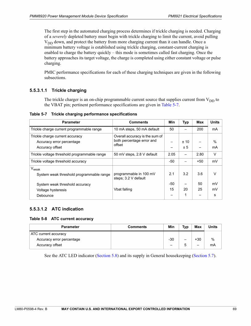
PMM8920 Power Management Module Device Specification PM8921 Electrical Specifications
LM80-P0598-4 Rev. B MAY CONTAIN U.S. AND INTERNATIONAL EXPORT CONTROLLED INFORMATION 69
The first step in the automated charging process determines if trickle charging is needed. Charging of a severely depleted battery must begin with trickle charging to limit the current, avoid pulling VDD down, and protect the battery from more charging current than it can handle. Once a minimum battery voltage is established using trickle charging, constant-current charging is enabled to charge the battery quickly – this mode is sometimes called fast charging. Once the battery approaches its target voltage, the charge is completed using either constant voltage or pulse charging.
PMIC performance specifications for each of these charging techniques are given in the following subsections.
5.5.3.1.1 Trickle charging
The trickle charger is an on-chip programmable current source that supplies current from VDD to the VBAT pin; pertinent performance specifications are given in Table 5-7.
5.5.3.1.2 ATC indication
See the ATC LED indicator (Section 5.8) and its supply in General housekeeping (Section 5.7).
Table 5-7 Trickle charging performance specifications
Parameter Comments Min Typ Max Units
Trickle charge current programmable range 10 mA steps, 50 mA default 50 – 200 mA
Trickle charge current accuracy
Accuracy error percentage
Accuracy offset
Overall accuracy is the sum of both percentage error and offset
–
–
± 10
± 5
–
–
%
mA
Trickle voltage threshold programmable range 50 mV steps, 2.8 V default 2.05 – 2.80 V
Trickle voltage threshold accuracy -50 – +50 mV
Vweak
System weak threshold programmable range
System weak threshold accuracy
Voltage hysteresis
Debounce
programmable in 100 mV steps; 3.2 V default
Vbat falling
2.1
-50
15
–
3.2
–
20
1
3.6
50
25
–
V
mV
mV
s
Table 5-8 ATC current accuracy
Parameter Comments Min Typ Max Units
ATC current accuracy
Accuracy error percentage
Accuracy offset
-30
–
–
5
+30
–
%
mA

PMM8920 Power Management Module Device Specification PM8921 Electrical Specifications
LM80-P0598-4 Rev. B MAY CONTAIN U.S. AND INTERNATIONAL EXPORT CONTROLLED INFORMATION 70
5.5.3.1.3 Constant current charging
Constant current charging uses closed-loop control of the pass transistor to regulate the total current (device electronics plus charging current) to match the programmed value (IMAXSEL). The PMIC parameters associated with constant current charging are specified in the following subsections:
External supply voltagesSection 5.5.2
Battery voltage detector Section 5.5.4.8
Charging current is a function of the external supply voltage (such as DC_IN) for a fixed battery voltage (VBAT). The charging current will be reduced significantly if DC_IN is not sufficiently larger than VBAT. An example curve showing the charging current versus DC_IN is shown with VBAT fixed at 4.1 V.
Charging current is also a function of the battery voltage for a fixed external supply voltage. Charging current drops off quickly as VBAT approaches DC_IN. An example curve showing the charging current versus VBAT is shown with DC_IN fixed at 5 V.
Additional performance specifications for constant current charging are not required.
5.5.3.1.4 Constant voltage charging
Once constant current charging of a lithium-ion battery is completed, the charging continues using constant voltage techniques. Specifications pertaining to constant voltage charging are addressed in this subsection.
PMIC support of constant voltage charging is very similar to its constant current mode: the battery MOSFET is closed and the pass transistor is closed-loop controlled. But in this case, the closed-loop control regulates the voltage at VBAT to match the programmed value VMAXSEL. This ensures the most accurate final battery voltage – lithium-ion battery manufacturers recommend a voltage accuracy of 1% or better at the end of charge.
The PM8921 IC parameters associated with constant voltage charging are specified in the following subsections:
External supply voltagesSection 5.5.2
Battery voltage detectorSection 5.5.4.8
Additional performance specifications are not required.
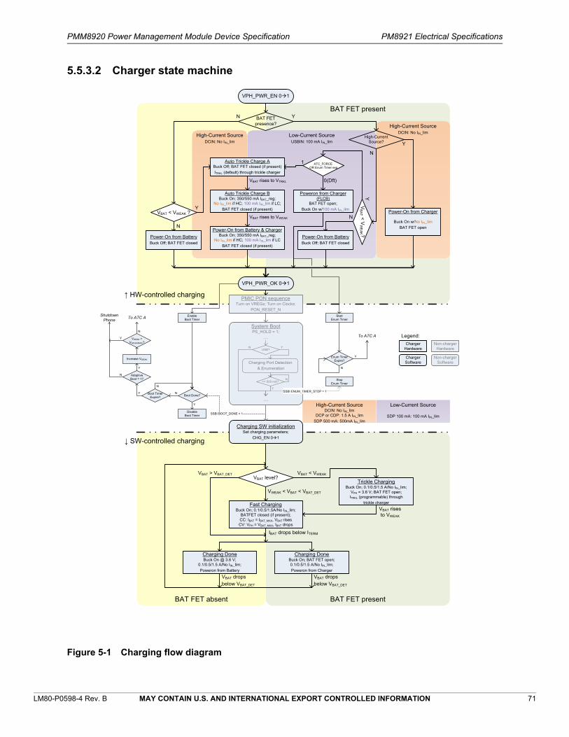
PMM8920 Power Management Module Device Specification PM8921 Electrical Specifications
LM80-P0598-4 Rev. B MAY CONTAIN U.S. AND INTERNATIONAL EXPORT CONTROLLED INFORMATION 71
5.5.3.2 Charger state machine
Figure 5-1 Charging flow diagram
High-Current SourceDCIN: No IIN_lim
DCP or CDP: 1.5 A IIN_limSDP 500 mA: 500mA IIN_lim
Low-Current Source
SDP 100 mA: 100 mA IIN_lim
System BootPS_HOLD = 1;
…
BAT FET present
BAT FET presentBAT FET absent
Low-Current SourceUSBIN: 100 mA IIN_lim
High-Current SourceDCIN: No IIN_limHigh-Current Source
DCIN: No IIN_lim
VBAT risesto VWEAK
PMIC PON sequenceTurn on VREGs; Turn on Clocks;
PON_RESET_N
VPH_PWR_EN 01
VPH_PWR_OK 01
Charging SW initializationSet charging parameters;
CHG_EN 01
BAT FETpresence?
N Y
Power-On from BatteryBuck Off; BAT FET closed
VBAT rises to VWEAK
Power-On from BatteryBuck Off; BAT FET closed
↑ HW-controlled charging
↓ SW-controlled charging
VBAT level?Trickle Charging
Buck On; 0.1/0.5/1.5 A/No IIN_lim;VPH = 3.6 V; BAT FET open;ITRKL (programmable) through
trickle chargerFast ChargingBuck On; 0.1/0.5/1.5A/No IIN_lim;
BATFET closed (if present);CC: IBAT = IBAT_MAX, VBAT risesCV: VPH = VBAT_MAX, IBAT drops
IBAT drops below ITERM
Charging DoneBuck On @ 3.6 V;
0.1/0.5/1.5 A/No IIN_lim;Poweron from Battery
Charging DoneBuck On; BAT FET open;0.1/0.5/1.5 A/No IIN_lim;Poweron from Charger
Auto Trickle Charge ABuck Off; BAT FET closed (if present)ITRKL (default) through trickle charger
VBAT rises to VTRKL
Poweron from Charger(FLCB)
BAT FET open;Buck On w/100 mA IIN_lim Power-On from Charger
Buck On w/No IIN_limBAT FET open
Auto Trickle Charge BBuck On; 350/550 mA IBAT_reg;
No IIN_lim if HC; 100 mA IIN_lim if LC;BAT FET closed (if present)
Power-On from Battery & ChargerBuck On; 350/550 mA IBAT_reg;
No IIN_lim if HC; 100 mA IIN_lim if LCBAT FET closed (if present)
1
0(Dft)
High-CurrentSource? Y
N
VBAT < VWEAK ?Y
N
VBAT <
VW
EAK ?Y
N
VBAT dropsbelow VBAT_DET
VBAT dropsbelow VBAT_DET
Charging Port Detection& Enumeration
VWEAK < VBAT < VBAT_DET
VBAT < VWEAKVBAT > VBAT_DET
Boot TimerExpire?
Increase VWEAK
VWEAK >VWEAK(MAX)?
AdaptiveBoot = 1?
Y
Boot Done?
Y
N
N
Y
N
Y
SSBI BOOT_DONE = 1
EnableBoot Timer
DisableBoot Timer
Enum TimerExpire?
StartEnum Timer
ChargerHardware
ChargerSoftware
Non-chargerHardware
Non-chargerSoftware
StopEnum Timer
USB?
>= 500 mA?
YN
…
N
YSSBI ENUM_TIMER_STOP = 1
N
Y
Legend:To ATC A
To ATC A
N
ShutdownPhone
ATC_FORCEOR Enum Timer exp
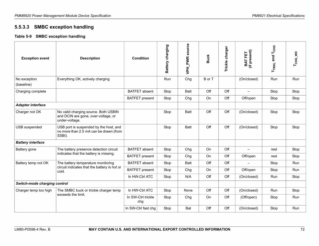
PMM8920 Power Management Module Device Specification PM8921 Electrical Specifications
LM80-P0598-4 Rev. B MAY CONTAIN U.S. AND INTERNATIONAL EXPORT CONTROLLED INFORMATION 72
5.5.3.3 SMBC exception handling
Table 5-9 SMBC exception handling
Exception event Description Condition
Ba
tter
y ch
arg
ing
VP
H_P
WR
so
urc
e
Bu
ck
Tric
kle
char
ger
BA
T F
ET
(i
f p
rese
nt)
TT
RK
L a
nd
TC
HG
TC
HG
_W
D
No exception
(baseline)
Everything OK, actively charging Run Chg B or T (On/closed) Run Run
Charging complete BATFET absent Stop Batt Off Off – Stop Stop
BATFET present Stop Chg On Off Off/open Stop Stop
Adapter interface
Charger not OK No valid charging source. Both USBIN and DCIN are gone, over-voltage, or under-voltage.
Stop Batt Off Off (On/closed) Stop Stop
USB suspended USB port is suspended by the host, and no more than 2.5 mA can be drawn (from SSBI).
Stop Batt Off Off (On/closed) Stop Stop
Battery interface
Battery gone The battery presence detection circuit indicates that the battery is missing.
BATFET absent Stop Chg On Off – rest Stop
BATFET present Stop Chg On Off Off/open rest Stop
Battery temp not OK The battery temperature monitoring circuit indicates that the battery is hot or cold.
BATFET absent Stop Batt Off Off – Stop Run
BATFET present Stop Chg On Off Off/open Stop Run
In HW-Ctrl ATC Stop N/A Off Off (On/closed) Run Stop
Switch-mode charging control
Charger temp too high The SMBC buck or trickle charger temp exceeds the limit.
In HW-Ctrl ATC Stop None Off Off (On/closed) Run Stop
In SW-Ctrl trickle chg
Stop Chg On Off (Off/open) Stop Run
In SW-Ctrl fast chg Stop Bat Off Off (On/closed) Stop Run

PMM8920 Power Management Module Device Specification PM8921 Electrical Specifications
LM80-P0598-4 Rev. B MAY CONTAIN U.S. AND INTERNATIONAL EXPORT CONTROLLED INFORMATION 73
Charging disabled SW disables charger via SSBI. BATFET absent Stop Batt Off Off – Stop & rest Stop
BATFET present Stop Chg Off Off Off/open Stop & rest Stop
Charging paused SW pauses battery charging via SSBI. BATFET absent Stop Batt Off Off – Stop Run
BATFET present Stop Chg On Off Off/open Stop Run
TTRKL expire Trickle charging timer expires. BATFET absent Stop Batt Off – Stop Stop
BATFET present Stop Chg On Off/open Stop Stop
TCHG expire Maximum charging timer expires. BATFET absent Stop Batt Off – Stop Stop
BATFET present Stop Chg On Off/open Stop Stop
TCHG_WD expire Charging SW not responding causing charger WD timer expires.
BATFET absent Stop Batt Off – Stop Stop
BATFET present Stop Chg On Off/open Stop Stop
VTRKL_FAULT VBAT rises above VTRKL_FAULT during trickle charging.
Stop Chg On Off/open Stop Stop
PMIC infrastructure Stop
VPH_PWR_EN: 1 --> 0 PON module requests the charger not to bring up VDD.
Stop Off Off Off/open Stop & rest Stop
PON not OK PON module gets stuck in the powerup sequence, or the APQ device fails to raise PS_HOLD.
Stop Chg On Off/open Stop Stop
CRIT_SHTDWN MBG not OK, or PMIC over-temperature stage 2 occurred.
In HW-Ctrl ATC Stop OFF Off/open Stop & rest Stop
Not in ATC Stop Stop
Table 5-9 SMBC exception handling (cont.)
Exception event Description Condition
Ba
tter
y ch
arg
ing
VP
H_P
WR
so
urc
e
Bu
ck
Tric
kle
char
ger
BA
T F
ET
(i
f p
rese
nt)
TT
RK
L a
nd
TC
HG
TC
HG
_W
D

PMM8920 Power Management Module Device Specification PM8921 Electrical Specifications
LM80-P0598-4 Rev. B MAY CONTAIN U.S. AND INTERNATIONAL EXPORT CONTROLLED INFORMATION 74
5.5.4 Battery monitoring system
The module provides function to monitor the battery capacity in conjunction with XOADC, which provides battery voltage information when needed.
5.5.4.1 Battery voltage alarm
A programmable window detector continuously monitors the battery voltage at VBAT. Both thresholds, upper and lower, are programmable and include voltage hysteresis to ensure stability. To prevent brief voltage transients from generating interrupts unnecessarily, the out-of-range condition must stay triggered for a certain amount of time before an interrupt is generated. This delay, referred to as time hysteresis, is also programmable. If the battery voltage returns in-range before the programmed delay, the delay timer is reset and no interrupt is generated.
Performance specifications for the battery voltage alarm circuits are given in Table 5-10.
5.5.4.2 UVLO
The device supply voltage (VDD) is monitored continuously by a UVLO circuit that automatically turns off the device at severely low VDD conditions. However, the programmable UVLO threshold is lower than the low battery threshold, described in Section 5.5.4.8.
Other than the programmable threshold, software is not involved in UVLO detection. Hysteresis and time delays are not programmable, and UVLO events do not generate interrupts. They are reported to the APQ or QSC devices via the PON_RESET_N signal. UVLO-related voltage and timing specifications are listed in Table 5-11.
Table 5-10 Battery voltage alarm performance specifications
Parameter Comments Min Typ Max Units
Programmable thresholds Programmable ranges, 25 mV steps for each and can be disabled entirely
2.800 – 5.600 V
Alarm accuracy Assuming 0.5% accuracy for 1.25 V reference -50 – +50 mV
Threshold voltage hysteresis
VBAT = 2.8 to 4.5 V
VBAT = 4.5 to 5.5 V
20
30 –
60
80
mV
mV
Time hysteresis Programmable range 0.125 – 16.0 ms
Table 5-11 UVLO performance specifications
Parameter Comments Min Typ Max Units
Threshold voltage, falling1122
1. The hardware UVLO threshold voltage of 2.7 V is set by a trim procedure.2. UVLO rising threshold = UVLO falling threshold + UVLO hysteresis. For PM8921, ULVO rising threshold = 2.7 V +
175 mV = 2.875 V.
Programmable value 1.500 2.700 3.050 V
Threshold voltage accuracy -5 – +5 %
Hysteresis 100 175 250 mV
UVLO detection interval – 1.0 – µs

PMM8920 Power Management Module Device Specification PM8921 Electrical Specifications
LM80-P0598-4 Rev. B MAY CONTAIN U.S. AND INTERNATIONAL EXPORT CONTROLLED INFORMATION 75
5.5.4.3 SMPL
The PMIC SMPL feature initiates a poweron sequence if the monitored phone voltage (VDD) drops out-of-range and then returns in-range within a programmable interval. When enabled by software, SMPL achieves immediate and automatic recovery from momentary power loss (such as a brief battery disconnect when the phone is jarred).
SMPL performance specifications are given in Table 5-12.
5.5.4.4 Battery MOSFET requirements
Battery transistor (Table 5-13) – this external P-channel MOSFET is required. Without it, depleted batteries could dangerously overheat when charging.
The specifications for the external battery MOSFET are intended for example purposes only. Device designers are encouraged to use their own choices while understanding that overall performance might be affected by an inappropriate choice.
5.5.4.5 Battery MOSFET driver
A control driver for the battery MOSFET is included within the PMIC; its drive signal is applied to the external transistor via the BAT_FET_N pin. Specifications for the battery MOSFET driver are listed in Table 5-14. Some specifications depend on suitable external components, as identified in Table 5-13 or they depend on the control mode, as identified in Table 5-14.
Table 5-12 SMPL performance specifications
Parameter Comments Min Typ Max Units
Minimum SMPL interval11 Programmable range 0.1 – 2.0 s
1. The timing accuracy of the SMPL interval is set entirely by the oscillator clocking the counters. Valid settings are: 0.5, 1.0, 1.5, and 2.0 seconds. With cal-RC disabled, these settings correspond to the external keep-alive capacitor value used at VCOIN: 1.5, 3.3, 4.7, and 6.8 F, respectively.
Table 5-13 External battery P-channel MOSFET specifications
Parameter Comments Min Typ Max Units
Example specifications based upon International Rectifier model IRF7324
Drain-source voltage – – -20 V
Continuous drain current VGS = -4.5 V, TA = +70°C – – -5.4 A
Pulsed drain current – – -40 A
Power dissipation TA = +70°C – – 1.3 W
Gate-to-source voltage -12 – +12 V
Junction temperature -55 – +150 °C
Thermal resistance Junction-to-ambient – – 62.5 °C/W
D-S on resistance Static, VGS = -2.5 V, ID = -6.0 A – – 0.026
Gate threshold voltage VDS = VGS, ID = -6.0 A -0.45 – -1.00 V
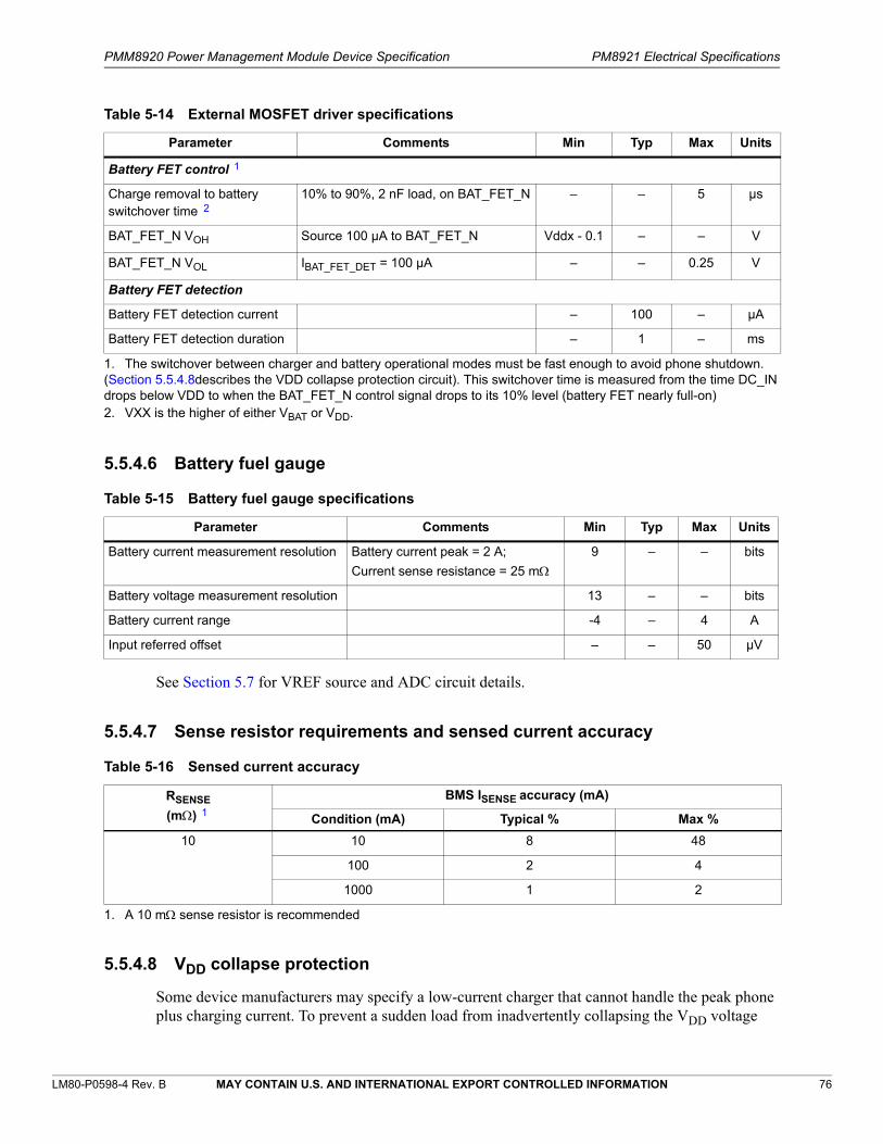
PMM8920 Power Management Module Device Specification PM8921 Electrical Specifications
LM80-P0598-4 Rev. B MAY CONTAIN U.S. AND INTERNATIONAL EXPORT CONTROLLED INFORMATION 76
5.5.4.6 Battery fuel gauge
See Section 5.7 for VREF source and ADC circuit details.
5.5.4.7 Sense resistor requirements and sensed current accuracy
5.5.4.8 VDD collapse protection
Some device manufacturers may specify a low-current charger that cannot handle the peak phone plus charging current. To prevent a sudden load from inadvertently collapsing the VDD voltage
Table 5-14 External MOSFET driver specifications
Parameter Comments Min Typ Max Units
Battery FET control11
1. The switchover between charger and battery operational modes must be fast enough to avoid phone shutdown. (Section 5.5.4.8describes the VDD collapse protection circuit). This switchover time is measured from the time DC_IN drops below VDD to when the BAT_FET_N control signal drops to its 10% level (battery FET nearly full-on)
Charge removal to battery switchover time22
2. VXX is the higher of either VBAT or VDD.
10% to 90%, 2 nF load, on BAT_FET_N – – 5 µs
BAT_FET_N VOH Source 100 µA to BAT_FET_N Vddx - 0.1 – – V
BAT_FET_N VOL IBAT_FET_DET = 100 µA – – 0.25 V
Battery FET detection
Battery FET detection current – 100 – µA
Battery FET detection duration – 1 – ms
Table 5-15 Battery fuel gauge specifications
Parameter Comments Min Typ Max Units
Battery current measurement resolution Battery current peak = 2 A;
Current sense resistance = 25 m9 – – bits
Battery voltage measurement resolution 13 – – bits
Battery current range -4 – 4 A
Input referred offset – – 50 µV
Table 5-16 Sensed current accuracy
RSENSE
(m)11
BMS ISENSE accuracy (mA)
Condition (mA) Typical % Max %
10 10 8 48
100 2 4
1000 1 2
1. A 10 m sense resistor is recommended

PMM8920 Power Management Module Device Specification PM8921 Electrical Specifications
LM80-P0598-4 Rev. B MAY CONTAIN U.S. AND INTERNATIONAL EXPORT CONTROLLED INFORMATION 77
when a low-current charger is used, the PMIC monitors the voltage across the battery MOSFET (through the VPH_PWR and VBAT pins) and automatically turns it on if VDD drops about 40 mV below VBAT.
Performance specifications related to VDD collapse protection are given in Table 5-17.
5.5.4.9 Battery temperature monitoring specifications
If the system does not use a BAT_ID pin, then the unused BAT_ID pin can be grounded.
Starting with ES2 and CS, if BATT_THERM is not needed, grounding the BATT_THERM pin is recommended, and it is necessary to disable the feature in the software.
Table 5-18 lists battery interface specifications.
Table 5-17 VDD collapse protection performance specifications
Parameter Comments Min Typ Max Units
BAT_FET_N output, 0 V differential VBAT - VPH_PWR = 0 V VDD - 0.1 – VDD V
VBAT - VPH_PWR VCP interrupt triggers 20 60 100 mV
Activation time – – 5 µs
Table 5-18 Battery interface specifications
Parameter Comments Min Typ Max Units
Battery-temperature monitoring
Cold-comparator threshold programmable settings
Fraction of VREF_BAT_THM 70 – 80 %
Cold-comparator offset -10 – 10 mV
Cold-comparator voltage hysteresis
70% setting
80% setting
VREF_BAT_THM falling (battery warming) -80
-70
–
–
-40
-35
mV
mV
Cold-comparator debounce VREF_BAT_THM rising or falling 1 – 2 s
Hot-comparator threshold programmable settings
Fraction of VREF_BAT_THM 25 – 35 %
Hot-comparator offset -10 – 10 mV
Hot-comparator voltage hysteresis
35% setting
25% setting
VREF_BAT_THM failing (battery cooling)
25
15
–
–
50
30
mV
mV
Hot-comparator debounce VREF_BAT_THM rising or falling 1 – 2 s
Battery presence detection (BPD)
BPD-comparator threshold Fraction of VREF_BAT_THM – 95 – %
BPD-comparator offset -50 – 50 mV
BPD-comparator debounce
VREF_BAT_THM rising (battery removal)
VREF_BAT_THM falling (battery insertion)
1
–
–
1
3
–
µs
s

PMM8920 Power Management Module Device Specification PM8921 Electrical Specifications
LM80-P0598-4 Rev. B MAY CONTAIN U.S. AND INTERNATIONAL EXPORT CONTROLLED INFORMATION 78
Figure 5-2 BTM diagram
Arb
iter
Battery temperature monitor
Battery presence detection
1.8 V LDO
BAT_COLD
BAT_HOT
VREG_L14
BAT_THM
SBI_ENEN CHG_EN
ADC_EN
BAT_ID
95%
AM
UX
XO/HKADC
80%
70%
35%
25%
CoolWarm
BATtemp
PM8921
BAT_GONEP
SI
BAT_ID_GONE
BAT_THM_GONE
CHG_GND
BMS_CSP
RS11%
RTHM1%
RS21%
RBID1%
RPU1%
VREF_BAT_THM 1.875V aVdd
1uF
VREG_OK
RSNS
Batterypack
BMS_CSN
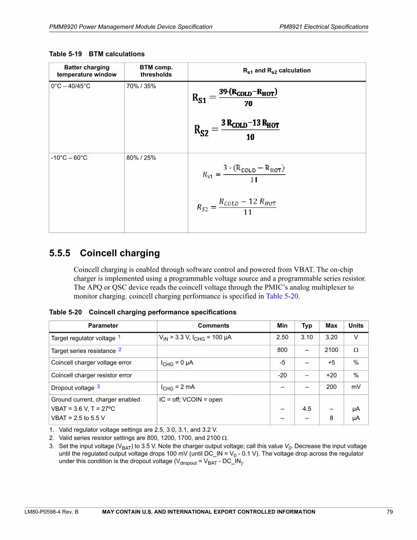
PMM8920 Power Management Module Device Specification PM8921 Electrical Specifications
LM80-P0598-4 Rev. B MAY CONTAIN U.S. AND INTERNATIONAL EXPORT CONTROLLED INFORMATION 79
5.5.5 Coincell charging
Coincell charging is enabled through software control and powered from VBAT. The on-chip charger is implemented using a programmable voltage source and a programmable series resistor. The APQ or QSC device reads the coincell voltage through the PMIC’s analog multiplexer to monitor charging. coincell charging performance is specified in Table 5-20.
Table 5-19 BTM calculations
Batter charging temperature window
BTM comp. thresholds
Rs1 and Rs2 calculation
0°C – 40/45°C 70% / 35%
-10°C – 60°C 80% / 25%
Table 5-20 Coincell charging performance specifications
Parameter Comments Min Typ Max Units
Target regulator voltage11 VIN > 3.3 V, ICHG = 100 µA 2.50 3.10 3.20 V
Target series resistance22 800 – 2100
Coincell charger voltage error ICHG = 0 µA -5 – +5 %
Coincell charger resistor error -20 – +20 %
Dropout voltage33 ICHG = 2 mA – – 200 mV
Ground current, charger enabled
VBAT = 3.6 V, T = 27ºC
VBAT = 2.5 to 5.5 V
IC = off; VCOIN = open
–
–
4.5
–
–
8
µA
µA
1. Valid regulator voltage settings are 2.5, 3.0, 3.1, and 3.2 V.2. Valid series resistor settings are 800, 1200, 1700, and 2100 .3. Set the input voltage (VBAT) to 3.5 V. Note the charger output voltage; call this value V0. Decrease the input voltage
until the regulated output voltage drops 100 mV (until DC_IN = V0 - 0.1 V). The voltage drop across the regulator under this condition is the dropout voltage (Vdropout = VBAT - DC_IN).

PMM8920 Power Management Module Device Specification PM8921 Electrical Specifications
LM80-P0598-4 Rev. B MAY CONTAIN U.S. AND INTERNATIONAL EXPORT CONTROLLED INFORMATION 80
5.6 Output power management
The PMIC includes all the regulated voltages needed for most wireless device applications. Independent regulated power sources are required for various electronic functions to avoid signal corruption between diverse circuits, support power management sequencing, and to meet different voltage level requirements. Thirty-two programmable voltage regulators are provided, and all are derived from a common bandgap reference circuit. A high-level summary of all regulators and their intended uses is presented in Table 5-21.
Table 5-21 Output power management summary
Function TypeDefault
voltage (V)44Specified range
(V)Programmable
rangeIrated(mA)
Default on
Notes/use on APQ8064E chipset
S1 Buck SMPS11 1.225 0.750 – 1.400 0.375 – 3.050 1500 Y Sub-regulation purposes
S2 Buck SMPS 1 1.300 1.000 – 1.400 0.375 – 3.050 1500 – APQ device digital core, RF power supply
S3 Buck SMPS 1 1.050 0.500 – 1.400 0.375 – 3.050 2000 Y APQ device VDD_CORE, USB
S4 Buck SMPS 1 1.800 1.700 – 1.900 0.375 – 3.050 1500 Y APQ device GP, off-chip memory, WCN3660 IC. Do not change from default.
S5 Buck SMPS 1.050 0.500 – 1.350 0.350 – 3.300 2000 – APQ device apps processor #1
S6 Buck SMPS 1.050 0.500 – 1.350 0.350 – 3.300 2000 – APQ device apps processor #2
S7 Buck SMPS 1.100 0.750 – 1.350 0.375 – 3.050 1500 – Sub-regulation purposes
S8 Buck SMPS 2.200 1.500 – 2.350 0.375 – 3.050 1500 – Codec and RF supplies
L1 NMOS LDO 1.050 1.000 – 1.450 0.750 – 1.525 150 Y APQ and multimedia XO
L2 NMOS LDO 1.200 1.100 – 1.450 0.750 – 1.525 150 – APQ device MIPI; APQ temp; audio core
L3 PMOS LDO22 3.075 3.000 – 3.300 0.750 – 4.900 150 Y USB power
L4 PMOS LDO 1.800 1.700 – 1.900 0.750 – 4.900 50 Y APQ device USB analog, PMIC clock driver. Do not change from default.
L5 PMOS LDO 2.950 2.750 – 3.000 0.750 – 4.900 400 Y eMCC
L5 is specifically characterized for a rated current of up to 400 mA.
L6 PMOS LDO33 2.950 2.750 – 3.000 0.750 – 4.900 600 Y SD/MCC
L7 PMOS LDO 2.950 2.750 – 3.000 0.750 – 4.900 150 Y VDD_P2
L8 PMOS LDO 2.800 1.800 – 3.000 0.750 – 4.900 300 – LCD1 MIPI
L9 PMOS LDO 2.850 2.600 – 3.000 0.750 – 4.900 300 – Sensors

PMM8920 Power Management Module Device Specification PM8921 Electrical Specifications
LM80-P0598-4 Rev. B MAY CONTAIN U.S. AND INTERNATIONAL EXPORT CONTROLLED INFORMATION 81
L10 PMOS LDO 2.900 2.600 – 3.300 0.750 – 4.900 600 – VDD_2P9V
L11 PMOS LDO 2.900 1.800 – 3.300 0.750 – 4.900 150 – MIPI
L12 NMOS LDO 1.200 1.100 – 1.500 0.750 – 1.525 150 – Camera MIPI
L14 PMOS LDO 1.800 1.700 – 1.900 0.750 – 4.900 50 – –
L15 PMOS LDO 2.950 1.800 – 3.300 0.750 – 4.900 150 – UIM
L16 PMOS LDO 2.800 2.600 – 3.000 0.750 – 4.900 300 – LCD2 MIPI
L17 PMOS LDO 2.950 1.800 – 3.600 0.750 – 4.900 150 – UIM
L18 NMOS LDO 1.300 1.000 – 1.500 0.750 – 1.525 150 – –
L19 – – – – – – –
L20 – – – – – – –
L21 PMOS LDO 1.900 1.700 – 2.100 0.750 – 4.900 150 – VIDEO, VDD_A2, BBRX
L22 PMOS LDO 2.600 1.700 – 2.850 0.750 – 4.900 150 – RF switches
L23 PMOS LDO 1.800 1.700 – 1.900 0.750 – 4.900 150 – PLL, HDMI, MIPI
L24 NMOS LDO 1.050 0.750 – 1.250 0.750 – 1.525 1200 Y MEM, PLL
L25 NMOS LDO 1.225 0.750 – 1.250 0.750 – 1.525 1200 Y DDR, TXADC
L26 NMOS LDO 1.050 0.750 – 1.250 0.750 – 1.525 1200 – QDSP processor
L27 NMOS LDO 1.050 0.750 – 1.250 0.750 – 1.525 1200 – QDSP processor
L28 NMOS LDO 1.050 0.750 – 1.500 0.750 – 1.525 1200 – QDSP processor
L29 PMOS LDO 1.900 1.700 – 2.200 0.750 – 4.900 150 – –
LVS1 Low V switch 1.800 – – 100 – VDD_1P8V
LVS2 Low V switch 1.200 – – 300 – VDD_MODEM
LVS3 Low V switch 1.800 – – 100 – APQ device Qfuse
LVS4 Low V switch 1.800 – – 100 – Sensors
LVS5 Low V switch 1.800 – – 100 – MIPI
LVS6 Low V switch 1.800 – – 100 – –
LVS7 Low V switch 1.800 – – 100 – Digital MIC, RFIC GPS & I/O; APQ I/O
Table 5-21 Output power management summary (cont.)
Function TypeDefault
voltage (V)44Specified range
(V)Programmable
rangeIrated(mA)
Default on
Notes/use on APQ8064E chipset
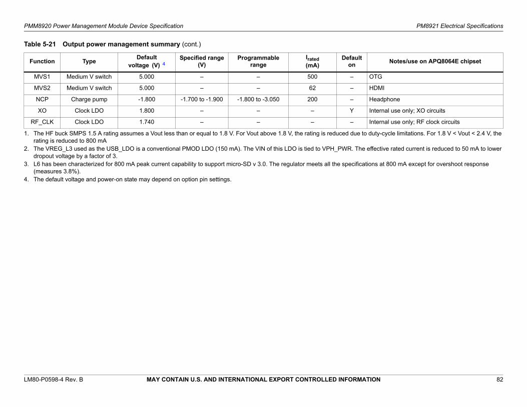
PMM8920 Power Management Module Device Specification PM8921 Electrical Specifications
LM80-P0598-4 Rev. B MAY CONTAIN U.S. AND INTERNATIONAL EXPORT CONTROLLED INFORMATION 82
MVS1 Medium V switch 5.000 – – 500 – OTG
MVS2 Medium V switch 5.000 – – 62 – HDMI
NCP Charge pump -1.800 -1.700 to -1.900 -1.800 to -3.050 200 – Headphone
XO Clock LDO 1.800 – – – Y Internal use only; XO circuits
RF_CLK Clock LDO 1.740 – – – – Internal use only; RF clock circuits
1. The HF buck SMPS 1.5 A rating assumes a Vout less than or equal to 1.8 V. For Vout above 1.8 V, the rating is reduced due to duty-cycle limitations. For 1.8 V < Vout < 2.4 V, the rating is reduced to 800 mA
2. The VREG_L3 used as the USB_LDO is a conventional PMOD LDO (150 mA). The VIN of this LDO is tied to VPH_PWR. The effective rated current is reduced to 50 mA to lower dropout voltage by a factor of 3.
3. L6 has been characterized for 800 mA peak current capability to support micro-SD v 3.0. The regulator meets all the specifications at 800 mA except for overshoot response (measures 3.8%).
4. The default voltage and power-on state may depend on option pin settings.
Table 5-21 Output power management summary (cont.)
Function TypeDefault
voltage (V)44Specified range
(V)Programmable
rangeIrated(mA)
Default on
Notes/use on APQ8064E chipset

PMM8920 Power Management Module Device Specification PM8921 Electrical Specifications
LM80-P0598-4 Rev. B MAY CONTAIN U.S. AND INTERNATIONAL EXPORT CONTROLLED INFORMATION 83
Output power management circuits include:
Bandgap voltage reference circuit
Buck SMPS circuits
LDO linear regulators
NCP
Voltage switches
All regulators can be set to a low-power mode, except VREG_NCP; the NCP output provides a negative voltage for headphone circuits. Details are provided in the following subsections.
5.6.1 Reference circuit
All PMIC regulator circuits and other internal circuits are driven by a common, on-chip voltage reference circuit. An on-chip series resistor supplements an off-chip 0.1 µF bypass capacitor at the REF_BYP pin to create a lowpass function that filters the reference voltage distributed throughout the device.
NOTE Do not load the REF_BYP pin. Use an MPP configured as an analog output if the reference voltage is needed off-chip.
Applicable voltage reference performance specifications are given in Table 5-22.
Table 5-22 Voltage reference performance specifications
Parameter Comments Min Typ Max Units
Nominal internal VREF At REF_BYP pin – 1.250 – V
Output voltage deviations
Normal operation
Normal operation
Sleep mode
Over temperature only, -20 to +120ºC
All operating conditions
All operating conditions
-0.32
-0.50
-1.00
–
–
–
+0.32
+0.50
+1.00
%
%
%
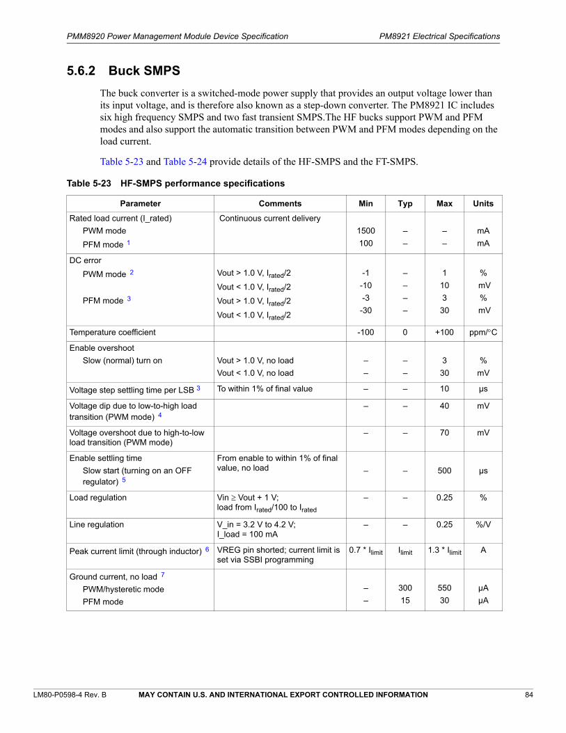
PMM8920 Power Management Module Device Specification PM8921 Electrical Specifications
LM80-P0598-4 Rev. B MAY CONTAIN U.S. AND INTERNATIONAL EXPORT CONTROLLED INFORMATION 84
5.6.2 Buck SMPS
The buck converter is a switched-mode power supply that provides an output voltage lower than its input voltage, and is therefore also known as a step-down converter. The PM8921 IC includes six high frequency SMPS and two fast transient SMPS.The HF bucks support PWM and PFM modes and also support the automatic transition between PWM and PFM modes depending on the load current.
Table 5-23 and Table 5-24 provide details of the HF-SMPS and the FT-SMPS.
Table 5-23 HF-SMPS performance specifications
Parameter Comments Min Typ Max Units
Rated load current (I_rated)
PWM mode
PFM mode11
Continuous current delivery
1500
100
–
–
–
–
mA
mA
DC error
PWM mode22
PFM mode33
Vout > 1.0 V, Irated/2
Vout < 1.0 V, Irated/2
Vout > 1.0 V, Irated/2
Vout < 1.0 V, Irated/2
-1
-10
-3
-30
–
–
–
–
1
10
3
30
%
mV
%
mV
Temperature coefficient -100 0 +100 ppm/C
Enable overshoot
Slow (normal) turn on Vout > 1.0 V, no load
Vout < 1.0 V, no load
–
–
–
–
3
30
%
mV
Voltage step settling time per LSB 3 To within 1% of final value – – 10 µs
Voltage dip due to low-to-high load transition (PWM mode)44
– – 40 mV
Voltage overshoot due to high-to-low load transition (PWM mode)
– – 70 mV
Enable settling time
Slow start (turning on an OFF regulator)55
From enable to within 1% of final value, no load – – 500 µs
Load regulation Vin Vout + 1 V; load from Irated/100 to Irated
– – 0.25 %
Line regulation V_in = 3.2 V to 4.2 V; I_load = 100 mA
– – 0.25 %/V
Peak current limit (through inductor)66 VREG pin shorted; current limit is set via SSBI programming
0.7 * Ilimit Ilimit 1.3 * Ilimit A
Ground current, no load77
PWM/hysteretic mode
PFM mode
–
–
300
15
550
30
µA
µA

PMM8920 Power Management Module Device Specification PM8921 Electrical Specifications
LM80-P0598-4 Rev. B MAY CONTAIN U.S. AND INTERNATIONAL EXPORT CONTROLLED INFORMATION 85
PWM / PFM transitions
Undershoot
Overshoot
Vout > 1.0 V, I_load = 20 mA
Vout < 1.0 V, I_load = 20 mA
Vout > 1.0 V, I_load = 20 mA
Vout < 1.0 V, I_load = 20 mA
–
–
–
–
–
–
–
–
3
40
3
40
%
mV
%
mV
Output ripple voltage
PWM pulse skipping mode88
PWM non-pulse skipping mode99
PFM mode 9
Tested at the switching frequency
40 mA load; 20 MHz measurement bandwidth
I_rated; 20 MHz measurement bw
20 mA load; 20 MHz measurement bandwidth
–
–
–
30
10
30
50
20
50
mVpp
mVpp
mVpp
Power supply ripple rejection (PSRR)
50 Hz to 1 kHz
1 kHz to 100 kHz
–
–
40
20
–
–
dB
dB
Efficiency1010
PWM mode
PFM mode
Vbat = 3.6 V
Vo = 1.8 V, Io = 300 mA
Vo = 1.8 V, Io = 10–600 mA
Vo = 1.8 V, Io = 800 mA
Vo = 1.2 V, Io = 5 mA
–
–
–
–
90
85
80
80
–
–
–
–
%
%
%
%
Output noise
F < 5 kHz
5 kHz < F < 10 kHz
10 kHz < F < 500 kHz
500 kHz < F < 1 MHz
F > 2 MHz
–
–
–
–
–
-95
-100
-100
-110
-110
–
–
–
–
–
dBm/Hz
dBm/Hz
dBm/Hz
dBm/Hz
dBm/Hz
1. Over the entire component range.2. Measured at the output capacitance at 25°C and trimmed voltage setting. The total DC error is the sum of DC error,
error due to the temperature coefficient, line regulation, and load regulation. This specification is for the default voltage setting.
3. Voltage step at 1 LSB (12.5 mV or 25 mV).4. Depending on the Imax performance over Vin/Vout/Fsw range and also depending on the values of the external L
and C used.5. Poweron soft-start: 500 µs; configurable soft-start: 100, 500 µs (fast, slow).6. This specification is for default current limit that is programmable. 7. Quiescent current (no switching). The ground current sleep current includes extra 50 µA to meet tolerance in peak
current Ilimit.8. Ripple dependent on the external components and layout.9. Ripple dependent on the external capacitor; capacitor < ESR 20 m10. Refer to Figure 3-3 to Figure 3-10 for efficiency plots.
Table 5-23 HF-SMPS performance specifications (cont.)
Parameter Comments Min Typ Max Units

PMM8920 Power Management Module Device Specification PM8921 Electrical Specifications
LM80-P0598-4 Rev. B MAY CONTAIN U.S. AND INTERNATIONAL EXPORT CONTROLLED INFORMATION 86
Table 5-24 2000 mA FT-SMPS performance specifications
Parameter Comments1122 Min Typ Max Unit
Rated load current (Irated)
Normal PWM mode
Low-power PFM mode
–
–
–
–
2000
100
mA
mA
V_OUT, programmable range
Option 1, power collapsed state
Option 2, active digital core
Option 3, other applications33
Selected in SW
50 mV increments
12.5 mV increments
50 mV increments
0.350
0.700
1.400
0.500
1.100
–
0.650
1.400
3.075
V
V
V
V_OUT, guaranteed performance 0.350 – 3.300 V
DC error44 At half rated current
V_OUT > 1.000 V
V_OUT < 1.000 V
-1
-10
0
0
+1
+10
%
mV
Temperature coefficient -100 0 +100 ppm/C
Transient response
Soft-start settling time at enable
Overshoot at enable
Load changes, PWM mode
Undershoot
Overshoot
Programmed voltage change
Overshoot
Settling time
To within 1% of final value
200 to 1500 mA load change
1500 to 200 mA load change
–
–
–
–
–
–
–
–
–
–
–
–
1
10
40
70
5
100
ms
%
mV
mV
%
s
Load regulation Vin > Vout + 1 V; Irated/100 to Irated – – 0.5 %
Line regulation Vin = 3.0 to 4.2 V – – 0.25 %/V
Output ripple, constant load
PWM (normal) mode
PFM (low-power) mode
–
–
–
–
20
50
mVpp
mVpp
PSRR
50 to 1000 Hz
1 to 100 kHz
Power supply ripple rejection ratio
–
–
50
30
–
–
dB
dB
Efficiency – PWM mode Refer to Figure 3-7 and Figure 3-8. – – –
Ground current
No load, PFM mode
No load, PWM mode
PFM – buck low-power mode
PWM – buck normal mode
–
–
35
800
60
1500
µA
µA
1. All specifications apply over the device's recommended operating conditions, load current range, and capacitor ESR range, unless noted otherwise.
2. Performance characteristics that may degrade if the rated output current is exceeded: voltage error, output ripple and efficiency
3. Range 3 is available for supporting other functions in addition to digital cores – digital I/Os, RF circuits, mixed signal functions, and peripherals.
4. Measured at the output capacitance at 25°C and trimmed voltage setting. The total DC error is the sum of DC error, error due to temperature coefficient, line regulation and load regulation.
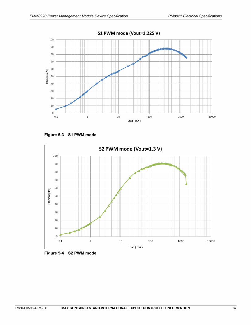
PMM8920 Power Management Module Device Specification PM8921 Electrical Specifications
LM80-P0598-4 Rev. B MAY CONTAIN U.S. AND INTERNATIONAL EXPORT CONTROLLED INFORMATION 87
Figure 5-3 S1 PWM mode
Figure 5-4 S2 PWM mode
0
10
20
30
40
50
60
70
80
90
100
0.1 1 10 100 1000 10000
Effic
ienc
y (%
)
Load ( mA )
S1 PWM mode (Vout=1.225 V)

PMM8920 Power Management Module Device Specification PM8921 Electrical Specifications
LM80-P0598-4 Rev. B MAY CONTAIN U.S. AND INTERNATIONAL EXPORT CONTROLLED INFORMATION 88
Figure 5-5 S3 PWM mode
Figure 5-6 S4 PWM mode
0
10
20
30
40
50
60
70
80
90
0.1 1 10 100 1000 10000
Effic
ienc
y (%
)
Load ( mA )
S3 PWM mode (Vout=1.05 V)
0
10
20
30
40
50
60
70
80
90
100
0.1 1 10 100 1000 10000
Effic
ienc
y (%
)
Load ( mA )
S4 PWM mode (Vout=1.8 V)
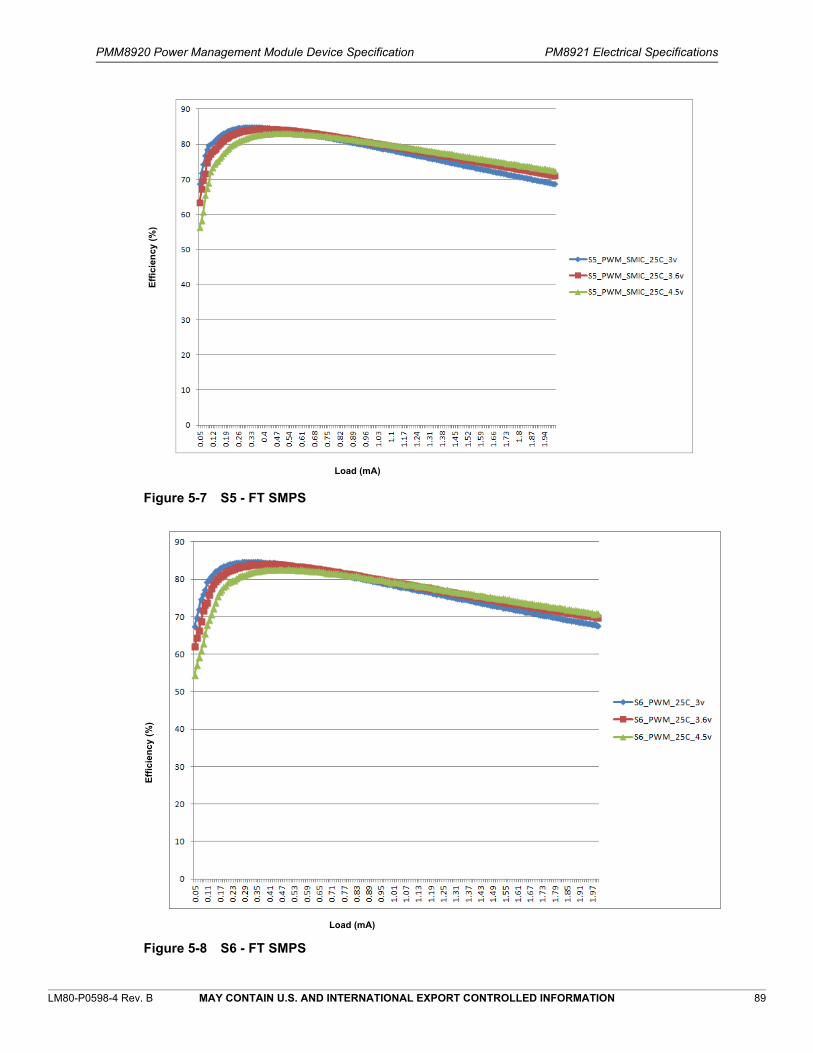
PMM8920 Power Management Module Device Specification PM8921 Electrical Specifications
LM80-P0598-4 Rev. B MAY CONTAIN U.S. AND INTERNATIONAL EXPORT CONTROLLED INFORMATION 89
Figure 5-7 S5 - FT SMPS
Figure 5-8 S6 - FT SMPS
Eff
icie
ncy
(%
)
Load (mA)
Eff
icie
nc
y (
%)
Load (mA)
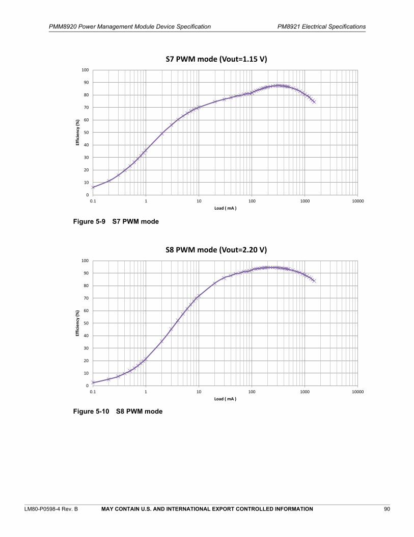
PMM8920 Power Management Module Device Specification PM8921 Electrical Specifications
LM80-P0598-4 Rev. B MAY CONTAIN U.S. AND INTERNATIONAL EXPORT CONTROLLED INFORMATION 90
Figure 5-9 S7 PWM mode
Figure 5-10 S8 PWM mode
0
10
20
30
40
50
60
70
80
90
100
0.1 1 10 100 1000 10000
Effic
ienc
y (%
)
Load ( mA )
S7 PWM mode (Vout=1.15 V)
0
10
20
30
40
50
60
70
80
90
100
0.1 1 10 100 1000 10000
Effic
ienc
y (%
)
Load ( mA )
S8 PWM mode (Vout=2.20 V)
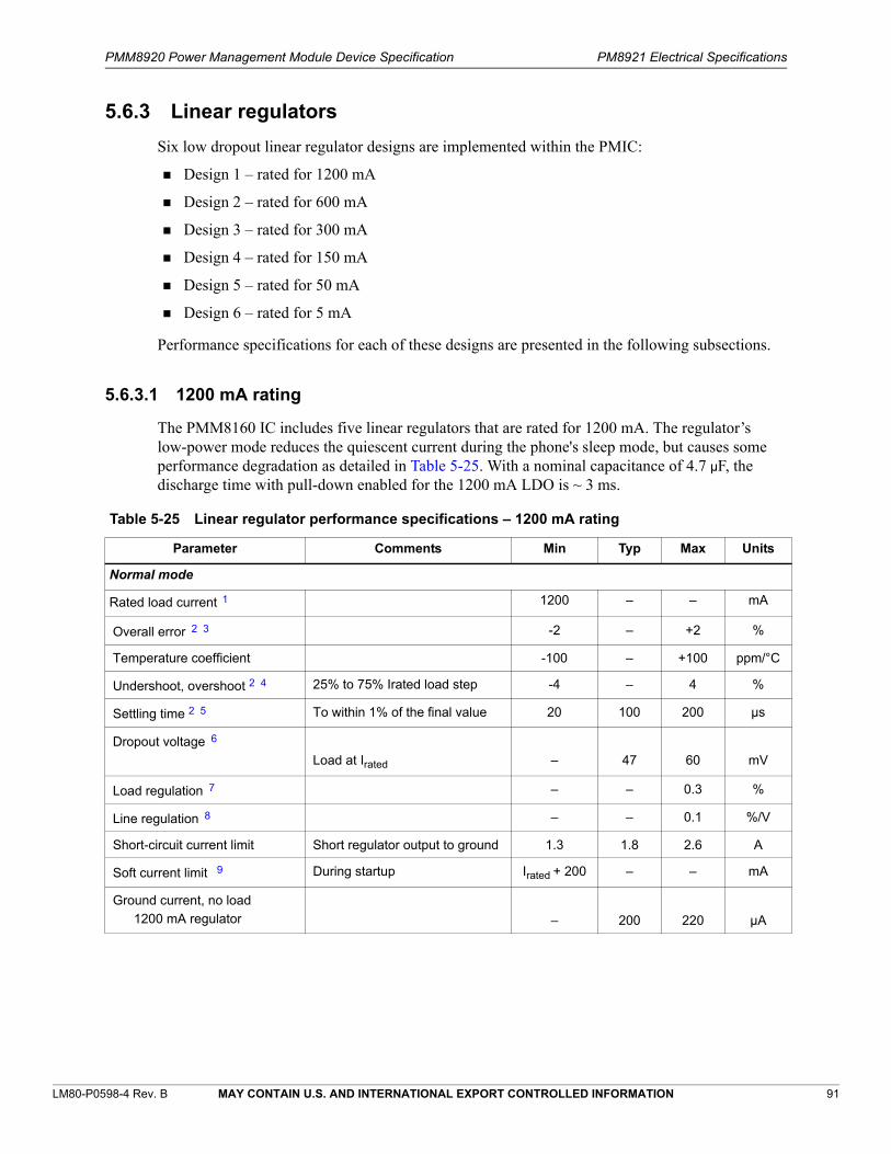
PMM8920 Power Management Module Device Specification PM8921 Electrical Specifications
LM80-P0598-4 Rev. B MAY CONTAIN U.S. AND INTERNATIONAL EXPORT CONTROLLED INFORMATION 91
5.6.3 Linear regulators
Six low dropout linear regulator designs are implemented within the PMIC:
Design 1 – rated for 1200 mA
Design 2 – rated for 600 mA
Design 3 – rated for 300 mA
Design 4 – rated for 150 mA
Design 5 – rated for 50 mA
Design 6 – rated for 5 mA
Performance specifications for each of these designs are presented in the following subsections.
5.6.3.1 1200 mA rating
The PMM8160 IC includes five linear regulators that are rated for 1200 mA. The regulator’s low-power mode reduces the quiescent current during the phone's sleep mode, but causes some performance degradation as detailed in Table 5-25. With a nominal capacitance of 4.7 µF, the discharge time with pull-down enabled for the 1200 mA LDO is ~ 3 ms.
Table 5-25 Linear regulator performance specifications – 1200 mA rating
Parameter Comments Min Typ Max Units
Normal mode
Rated load current11 1200 – – mA
Overall error2233 -2 – +2 %
Temperature coefficient -100 – +100 ppm/°C
Undershoot, overshoot 244 25% to 75% Irated load step -4 – 4 %
Settling time 255 To within 1% of the final value 20 100 200 µs
Dropout voltage66
Load at Irated – 47 60 mV
Load regulation77 – – 0.3 %
Line regulation88 – – 0.1 %/V
Short-circuit current limit Short regulator output to ground 1.3 1.8 2.6 A
Soft current limit 99 During startup Irated + 200 – – mA
Ground current, no load
1200 mA regulator – 200 220 µA

PMM8920 Power Management Module Device Specification PM8921 Electrical Specifications
LM80-P0598-4 Rev. B MAY CONTAIN U.S. AND INTERNATIONAL EXPORT CONTROLLED INFORMATION 92
Low-power mode
Rated load current 1 100 – – mA
Overall error 2 3 -4 – +4 %
Undershoot, overshoot 2 4 25% to 75% Irated load step -3 – +3 %
Dropout voltage
LV NMOS LDO (1200 mA) 6 – – 60 mV
Load regulation 7 – – 1 %
Line regulation 8 – – 0.5 %/V
Ground current, no load
1200 mA regulators – 21 25 µA
Normal mode and low-power mode
Ground current, with load – – 0.5 %
Bypass mode
Ground current – 4 5 µA
1. The rated current is the current at which the regulator meets all specifications.2. These specifications are met through the full device-operating range, load-current range, capacitor-ESR range, and
process corners, unless otherwise noted.3. The overall error is the sum of DC error, error due to temperature coefficient, line regulation, and load regulation.4. Overshoot and undershoot specifications are met with the rated load capacitance, at any of the following conditions:
startup, any load-step change, line-voltage change, program-voltage change, and transitions between normal and low-power modes. For low-power mode, only transitions between normal and low-power modes, load change (within limit), and line change apply.
5. The regulator always turns on in normal mode. The settling time is for startup, and for any voltage change with the rated load capacitance. Time will be increased with larger load capacitance.
6. Dropout voltage is defined as follows:a. Apply the specified load current.b. Set Vin = Vout + 0.5 V.c. Measure the output voltage.d. Reduce Vin until Vout is reduced by 100 mV.e. Calculate dropout voltage as Vin - Vout in this condition.
7. Load regulation is calculated as the output change in percent, when Vi > Vo + 0.5 V, with load changing from Irated/100 to Irated: (Vo2 - Vo1) / Vo1.
8. Line regulation is the output-voltage variation with respect to input-voltage variation, and can be calculated as: [(Vo2 - Vo1)/Vo1] / (Vi2 - Vi1).
9. The peak in-rush current must remain within this specification. A soft current limit is required to avoid too much instantaneous current draw from the battery, while still meeting the turn-on time requirement.
Table 5-25 Linear regulator performance specifications – 1200 mA rating (cont.)
Parameter Comments Min Typ Max Units
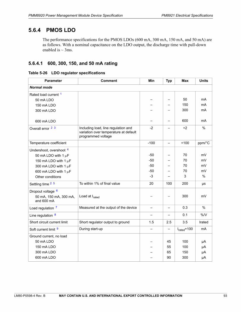
PMM8920 Power Management Module Device Specification PM8921 Electrical Specifications
LM80-P0598-4 Rev. B MAY CONTAIN U.S. AND INTERNATIONAL EXPORT CONTROLLED INFORMATION 93
5.6.4 PMOS LDO
The performance specifications for the PMOS LDOs (600 mA, 300 mA, 150 mA, and 50 mA) are as follows. With a nominal capacitance on the LDO output, the discharge time with pull-down enabled is ~ 3ms.
5.6.4.1 600, 300, 150, and 50 mA rating
Table 5-26 LDO regulator specifications
Parameter Comment Min Typ Max Units
Normal mode
Rated load current11
50 mA LDO
150 mA LDO
300 mA LDO
600 mA LDO
–
–
–
–
–
–
–
–
50
150
300
600
mA
mA
mA
mA
Overall error2233 Including load, line regulation and variation over temperature at default programmed voltage
-2 – +2 %
Temperature coefficient -100 – +100 ppm/°C
Undershoot, overshoot44
50 mA LDO with 1 F
150 mA LDO with 1 F
300 mA LDO with 1 F
600 mA LDO with 1 F
Other conditions
-50
-50
-50
-50
-3
–
–
–
–
–
70
70
70
70
3
mV
mV
mV
mV
%
Settling time 255 To within 1% of final value 20 100 200 µs
Dropout voltage66
50 mA, 150 mA, 300 mA, and 600 mA
Load at Irated – – 300 mV
Load regulation77 Measured at the output of the device – – 0.3 %
Line regulation88 – – 0.1 %/V
Short circuit current limit Short regulator output to ground 1.5 2.5 3.5 Irated
Soft current limit99 During start-up – – Irated+100 mA
Ground current, no load
50 mA LDO
150 mA LDO
300 mA LDO
600 mA LDO
–
–
–
–
45
55
65
90
100
100
150
300
µA
µA
µA
µA

PMM8920 Power Management Module Device Specification PM8921 Electrical Specifications
LM80-P0598-4 Rev. B MAY CONTAIN U.S. AND INTERNATIONAL EXPORT CONTROLLED INFORMATION 94
Low-power mode
Rated load current 1
50 mA LDO
150 mA LDO
300 mA LDO
600 mA LDO
–
–
–
–
–
–
–
–
5
10
10
10
mA
mA
mA
mA
Overall error 2 3 -4 – +4 %
Undershoot, overshoot -3 – 3 %
Dropout voltage 6
50 mA, 150 mA, 300 mA, and 600 mA
Load at Irated
– – 300 mV
Load regulation 7 – – 1.5 %
Line regulation 8 – – 0.5 %/V
Ground current, no load
50 mA LDO
150 mA LDO
300 mA LDO
600 mA LDO
–
–
–
–
5
5
5
5
6
6
6
6
µA
µA
µA
µA
Normal mode and low-power mode
Ground current, with load – – 0.2 %
1. The rated current is the current at which the regulator meets all specifications.2. These specifications are met through the full device-operating range, load-current range, capacitor-ESR range,
and process corners, unless otherwise noted.3. The overall error is the sum of DC error, error due to temperature coefficient, line regulation, and load regulation.4. PMOS LDO overshoot and undershoot specifications due to load transients are met with rated load capacitance
when Vi > Vo + 0.5 V, with load changing from Irated/100 to Irated. Overshoot and undershoot specifications due to other conditions are met with rated load capacitance when Vi > Vo + 0.5 V in the following conditions: line-voltage change by 1 V, low-power mode to normal-power mode transitions and vice-versa, and LDO startup.
5. The regulator always turns on in normal mode. The settling time is for startup, and for any voltage change with the rated load capacitance. Time will be increased with larger load capacitance.
6. Dropout voltage is defined as follows:a. Apply the specified load current.b. Set Vin = Vout + 0.5 V.c. Measure the output voltage.d. Reduce Vin until Vout is reduced by 100 mV.e. Calculate dropout voltage as Vin - Vout in this condition.
7. Load regulation is calculated as the output change in percent, when Vi > Vo + 0.5 V, with load changing from Irated/100 to Irated: (Vo2 - Vo1) / Vo1.
8. Line regulation is the output-voltage variation with respect to input-voltage variation, and can be calculated as: [(Vo2 - Vo1)/Vo1] / (Vi2 - Vi1)
9. The peak in-rush current must remain within this specification. A soft current limit is required to avoid too much instantaneous current draw from the battery, while still meeting the turn-on time requirement.
Table 5-26 LDO regulator specifications (cont.)
Parameter Comment Min Typ Max Units
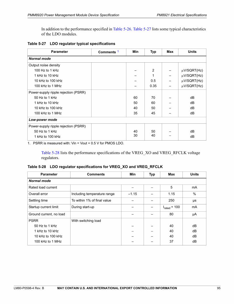
PMM8920 Power Management Module Device Specification PM8921 Electrical Specifications
LM80-P0598-4 Rev. B MAY CONTAIN U.S. AND INTERNATIONAL EXPORT CONTROLLED INFORMATION 95
In addition to the performance specified in Table 5-26, Table 5-27 lists some typical characteristics of the LDO modules.
Table 5-28 lists the performance specifications of the VREG_XO and VREG_RFCLK voltage regulators.
Table 5-27 LDO regulator typical specifications
Parameter Comments11 Min Typ Max Units
Normal mode
Output noise density
100 Hz to 1 kHz
1 kHz to 10 kHz
10 kHz to 100 kHz
100 kHz to 1 MHz
–
–
–
–
2
1
0.5
0.35
–
–
–
–
V/SQRT(Hz)
V/SQRT(Hz)
V/SQRT(Hz)
V/SQRT(Hz)
Power-supply ripple rejection (PSRR)
50 Hz to 1 kHz
1 kHz to 10 kHz
10 kHz to 100 kHz
100 kHz to 1 MHz
60
50
40
35
70
60
50
45
–
–
–
–
dB
dB
dB
dB
Low-power mode
Power-supply ripple rejection (PSRR)
50 Hz to 1 kHz
1 kHz to 100 kHz
4030
5040
––
dB
dB
1. PSRR is measured with: Vin = Vout + 0.5 V for PMOS LDO.
Table 5-28 LDO regulator specifications for VREG_XO and VREG_RFCLK
Parameter Comments Min Typ Max Units
Normal mode
Rated load current – – 5 mA
Overall error Including temperature range –1.15 – 1.15 %
Settling time To within 1% of final value – – 250 µs
Startup current limit During start-up – – Irated + 100 mA
Ground current, no load – – 80 µA
PSRR
50 Hz to 1 kHz
1 kHz to 10 kHz
10 kHz to 100 kHz
100 kHz to 1 MHz
With switching load
–
–
–
–
–
–
–
–
40
40
40
37
dB
dB
dB
dB

PMM8920 Power Management Module Device Specification PM8921 Electrical Specifications
LM80-P0598-4 Rev. B MAY CONTAIN U.S. AND INTERNATIONAL EXPORT CONTROLLED INFORMATION 96
5.6.5 NMOS LDO
The detailed specifications for the NMOS LDOs are detailed in Table 5-29.
Table 5-29 Linear regulator performance specifications – 150 mA rating
Parameter Comments Min Typ Max Units
Normal mode
Rated load current11 – – 150 mA
Overall error2233 -2 – +2 %
Temperature coefficient -100 – +100 ppm/°C
Undershoot, overshoot44 -3 – 3 %
Settling time 255 To within 1% of final value 20 100 200 µs
Dropout voltage66
NMOS LDO (150 mA, 300 mA)
Load at Irated
– – 200 mV
Load regulation77 – – 0.3 %
Line regulation88 – – 0.1 %/V
Short circuit current limit Short regulator output to gnd 2 3 4 Irated
Soft current limit99 During startup – – Irated + 100 mA
Ground current, no load – 100 150 µA
Low-power mode
Rated load current 1 – – 10 mA
Overall error 2 3 -4 – +4 %
Undershoot, overshoot 4 -3 – 3 %
Dropout voltage 6 Load at Irated – – 200 mV
Load regulation 7 – – 1.5 %
Line regulation 8 – – 0.5 %/V
Ground current, no load – 5 6 µA
Normal mode and low-power mode
Ground current, with load – – 0.5 %
Bypass mode
Ground current – – 1 µA
On resistance – – 1
1. The rated current is the current at which the regulator meets all specifications.2. These specifications are met through the full device-operating range, load-current range, capacitor-ESR range,
and process corners, unless otherwise noted.3. The overall error is the sum of DC error, error due to temperature coefficient, line regulation, and load regulation.4. NMOS LDO overshoot and undershoot specifications due to load transients are met with rated load capacitance
when Vi > Vo + 0.5 V, with load changing from Irated/100 to Irated, and at any of the following conditions: startup, any load-step change, line-voltage change, program-voltage change, and low-power mode to normal-power mode transitions (and vice-versa).
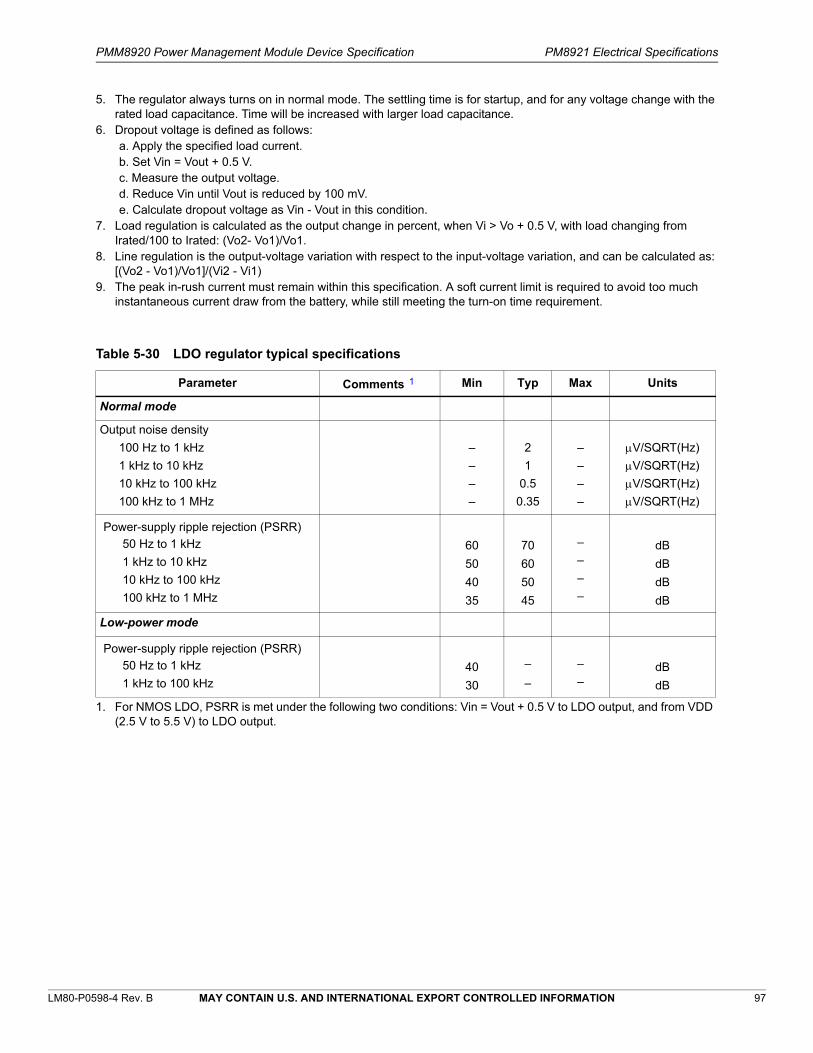
PMM8920 Power Management Module Device Specification PM8921 Electrical Specifications
LM80-P0598-4 Rev. B MAY CONTAIN U.S. AND INTERNATIONAL EXPORT CONTROLLED INFORMATION 97
5. The regulator always turns on in normal mode. The settling time is for startup, and for any voltage change with the rated load capacitance. Time will be increased with larger load capacitance.
6. Dropout voltage is defined as follows:a. Apply the specified load current.b. Set Vin = Vout + 0.5 V.c. Measure the output voltage.d. Reduce Vin until Vout is reduced by 100 mV.e. Calculate dropout voltage as Vin - Vout in this condition.
7. Load regulation is calculated as the output change in percent, when Vi > Vo + 0.5 V, with load changing from Irated/100 to Irated: (Vo2- Vo1)/Vo1.
8. Line regulation is the output-voltage variation with respect to the input-voltage variation, and can be calculated as: [(Vo2 - Vo1)/Vo1]/(Vi2 - Vi1)
9. The peak in-rush current must remain within this specification. A soft current limit is required to avoid too much instantaneous current draw from the battery, while still meeting the turn-on time requirement.
Table 5-30 LDO regulator typical specifications
Parameter Comments11 Min Typ Max Units
Normal mode
Output noise density
100 Hz to 1 kHz
1 kHz to 10 kHz
10 kHz to 100 kHz
100 kHz to 1 MHz
–
–
–
–
2
1
0.5
0.35
–
–
–
–
V/SQRT(Hz)
V/SQRT(Hz)
V/SQRT(Hz)
V/SQRT(Hz)
Power-supply ripple rejection (PSRR)
50 Hz to 1 kHz
1 kHz to 10 kHz
10 kHz to 100 kHz
100 kHz to 1 MHz
60
50
40
35
70
60
50
45
–
–
–
–
dB
dB
dB
dB
Low-power mode
Power-supply ripple rejection (PSRR)
50 Hz to 1 kHz
1 kHz to 100 kHz40
30
–
–
–
–dB
dB
1. For NMOS LDO, PSRR is met under the following two conditions: Vin = Vout + 0.5 V to LDO output, and from VDD (2.5 V to 5.5 V) to LDO output.

PMM8920 Power Management Module Device Specification PM8921 Electrical Specifications
LM80-P0598-4 Rev. B MAY CONTAIN U.S. AND INTERNATIONAL EXPORT CONTROLLED INFORMATION 98
5.6.6 NCP
The PMIC includes a capacitor-based NCP switching regulator that generates a negative 1.8 V (-1.8 V) supply for capless stereo headphone drivers. Pertinent performance specifications are listed in Table 5-31.
Table 5-31 NCP regulator performance specifications
Parameter Comments Min Typ Max Units
Switching frequency Programmable11 0.6 1.6 9.6 MHz
Output voltage Programmable 12 -2.4 -1.8 -1.5 V
Load current range 1 0 – 186 mA
Output error Zero load33 – – 50 mV
Transient overshoot -200 – 100 mV
Line regulation 3
Up to 50 mA load
Up to 186 mA load
–
–
20
25
50
65
mV/A
V/A
PSRR
at 2 kHz
at 5 kHz
at 20 kHz
pVdd to output
-15
-15
-15
-30
-30
-25
–
–
–
dB
dB
dB
Output ripple – 150 350 mV
Load regulation 3
Up to 93 mA load
Up to 150 mA load
Up to 186 mA load
–
–
–
0.1
0.1
0.1
0.2
0.3
0.4
V/A
V/A
V/A
1. All performance specifications are determined with default output voltage (-1.8 V) and frequency (1.6 MHz) settings, using 0402 X5R 2.2 µF 6.3 V capacitors from Taiyo Yuden Co., maximum load 186 mA, 2.5 V to 5.5 V unregulated input voltage, and operating in “non-sampling” mode.
2. Maximum deviation in output under a given load calculated as follows: (output error + (load regulation * load current) + (line regulation * pVdd variation)).
3. Performance specifications are not guaranteed for an output voltage beyond -1.8 V. Notable degradation in load regulation and other specifications may be observed beyond -1.8 V.

PMM8920 Power Management Module Device Specification PM8921 Electrical Specifications
LM80-P0598-4 Rev. B MAY CONTAIN U.S. AND INTERNATIONAL EXPORT CONTROLLED INFORMATION 99
5.6.7 Voltage switches
The PM8921 has seven low-voltage switches and two medium-voltage switches. The LVS are rated for 100 mA and 300 mA, while the MVS are rated for 100 mA and 500 mA and are used for gating the supply voltages to external circuits like BT, WLAN, UBM and other functions. LVS 1, 3, 4, 5, 6, and 7 are 100 mA LVS, whereas LVS 2 is a 300 mA LVS. The performance specifications for these switches are listed in Table 5-32.
Table 5-32 100 mA low-voltage switch specifications
Parameter Comments Min Typ Max Units
Load current Normal operation – – 100 mA
Input voltage range 1.0 – 1.8 V
Soft start time11 C_load < 1 μF – – 200 μs
Soft start inrush 2 C_load < 1 μF – – 200 mA
On resistance22 The on resistance of the switch – – 0.1 Ω
Ground current33
Sleep mode
Normal mode, no load
Normal mode, with load
–
–
–
–
–
–
1
30
30 + 0.03%
μA
μA
μA
1. The load cap should be less than 1μF.2. This specification is measured via the voltage drop and the load current 3. Sleep current means the quiescent current in sleep mode. Sleep mode means only switch is on and all the other
functions are disabled. This module does not provide power supply noise rejection.
Table 5-33 300 mA low-voltage switch specifications
Parameter Comments Min Typ Max Units
Rated current (Irated) Normal operation – 300 – mA
Slew rate (switch output node) Always – – 100 mV/µs
Switch output ready11 Startup 100 300 1200 µs
Input voltage range 1.2 – 1.875 V
On resistance Switch is on (fully enhanced) – – 150 m
Ground current
Sleep mode
Normal mode
–
–
–
–
1
40
µA
µA
Pull-down discharge time Switch is off – – 2 ms
1. This includes soft start time and gate full enhancement time.

PMM8920 Power Management Module Device Specification PM8921 Electrical Specifications
LM80-P0598-4 Rev. B MAY CONTAIN U.S. AND INTERNATIONAL EXPORT CONTROLLED INFORMATION 100
Table 5-34 65 mA MVS (HDMI) switch specifications
Parameter Comments Min Typ Max Units
Rated current (Irated)11 Normal operation 65 – – mA
Switch output ready22 Startup – – 200 μs
Input voltage range 4.0 – 5.5 V
On resistance – – 2000 mΩ
Ground current
Sleep mode
Normal mode
–
–
10
40
200
–
µA
µA
Pull-down discharge time – 0.5 2 ms
Steady-state reverse bias current At 5.5 V output – 20 – nA
Steady-state leakage current At 9.0 V output – 20 – nA
Leakage current at max transient At 9.0 V output – 350 – mA
1. Other rated currents may be required in the future.2. Switch output ready means that the switch is fully enhanced, which includes the time to acquire Vout_OK, plus the
time to fully enhance the switch (pull gate voltage to zero).
Table 5-35 500 mA MVS (OTG) switch specifications
Parameter Comments Min Typ Max Units
Rated current (Irated)11 Normal operation 500 – – mA
Switch output ready 22 Startup – – 200 μs
Input voltage range 4.0 – 5.5 V
On resistance – – 200 mΩ
Ground current
Sleep mode
Normal mode
–
–
10
40
200
–
μA
μA
Pull-down discharge time – 0.5 2 ms
Steady-state reverse bias current At 5.5 V output – 20 – nA
Steady-state leakage current 9.0 V output – 20 – nA
Leakage current at max transient 9.0 V output – 350 – mA
1. Other rated currents may be required in the future.2. Switch output ready means that the switch is fully enhanced, which includes the time to acquire Vout_OK, plus the
time to fully enhance the switch (pull gate voltage to zero).
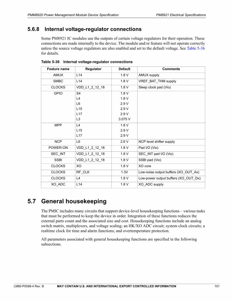
PMM8920 Power Management Module Device Specification PM8921 Electrical Specifications
LM80-P0598-4 Rev. B MAY CONTAIN U.S. AND INTERNATIONAL EXPORT CONTROLLED INFORMATION 101
5.6.8 Internal voltage-regulator connections
Some PM8921 IC modules use the outputs of certain voltage regulators for their operation. These connections are made internally to the device. The module and/or feature will not operate correctly unless the source voltage regulators are also enabled and set to the default voltage. See Table 5-36 for details.
5.7 General housekeeping
The PMIC includes many circuits that support device-level housekeeping functions – various tasks that must be performed to keep the device in order. Integration of these functions reduces the external parts count and the associated size and cost. Housekeeping functions include an analog switch matrix, multiplexers, and voltage scaling; an HK/XO ADC circuit; system clock circuits; a realtime clock for time and alarm functions; and overtemperature protection.
All parameters associated with general housekeeping functions are specified in the following subsections.
Table 5-36 Internal voltage-regulator connections
Feature name Regulator Default Comments
AMUX L14 1.8 V AMUX supply
SMBC L14 1.8 V VREF_BAT_THM supply
CLOCKS VDD_L1_2_12_18 1.8 V Sleep clock pad (Vio)
GPIO S4
L4
L6
L15
L17
L3
1.8 V
1.8 V
2.9 V
2.9 V
2.9 V
3.075 V
MPP L4
L15
L17
1.8 V
2.9 V
2.9 V
NCP L6 2.6 V NCP level shifter supply
POWER-ON VDD_L1_2_12_18 1.8 V Pad I/O (Vio)
SEC_INT VDD_L1_2_12_18 1.8 V SEC_INT pad I/O (Vio)
SSBI VDD_L1_2_12_18 1.8 V SSBI pad (Vio)
CLOCKS XO 1.8 V XO core
CLOCKS RF_CLK 1.3V Low-noise output buffers (XO_OUT_Ax)
CLOCKS L4 1.8 V Low-power output buffers (XO_OUT_Dx)
XO_ADC L14 1.8 V XO_ADC supply
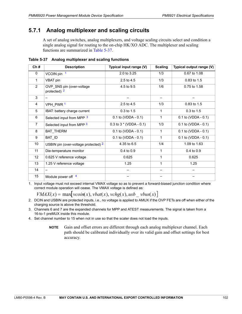
PMM8920 Power Management Module Device Specification PM8921 Electrical Specifications
LM80-P0598-4 Rev. B MAY CONTAIN U.S. AND INTERNATIONAL EXPORT CONTROLLED INFORMATION 102
5.7.1 Analog multiplexer and scaling circuits
A set of analog switches, analog multiplexers, and voltage scaling circuits select and condition a single analog signal for routing to the on-chip HK/XO ADC. The multiplexer and scaling functions are summarized in Table 5-37.
NOTE Gain and offset errors are different through each analog multiplexer channel. Each path should be calibrated individually over its valid gain and offset settings for best accuracy.
Table 5-37 Analog multiplexer and scaling functions
Ch # Description Typical input range (V) Scaling Typical output range (V)
0 VCOIN pin 11 2.0 to 3.25 1/3 0.67 to 1.08
1 VBAT pin 2.5 to 4.5 1/3 0.83 to 1.5
2 OVP_SNS pin (over-voltage protected)22
4.5 to 9.5 1/6 0.75 to 1.58
3 – – – –
4 VPH_PWR 1 2.5 to 4.5 1/3 0.83 to 1.5
5 IBAT: battery charge current 0.3 to 1.5 1 0.3 to 1.5
6 Selected input from MPP33 0.1 to (VDDA - 0.1) 1 0.1 to (VDDA - 0.1)
7 Selected input from MPP 3 0.3 to 3 * (VDDA - 0.1) 1/3 0.1 to (VDDA - 0.1)
8 BAT_THERM 0.1 to (VDDA - 0.1) 1 0.1 to (VDDA - 0.1)
9 BAT_ID 0.1 to (VDDA - 0.1) 1 0.1 to (VDDA - 0.1)
10 USBIN pin (over-voltage protected) 2 4.35 to 6.5 1/4 1.09 to 1.63
11 Die-temperature monitor 0.4 to 0.9 1 0.4 to 0.9
12 0.625 V reference voltage 0.625 1 0.625
13 1.25 V reference voltage 1.25 1 1.25
14 – – – –
15 Module power off 44 – – –
1. Input voltage must not exceed internal VMAX voltage so as to prevent a forward-biased junction condition where correct module operation will cease. The VMAX voltage is defined as:
2. DCIN and USBIN are protected inputs, i.e., no voltage is applied to AMUX if the OVP FETs are off when either of the charging source is above the threshold.
3. Channels 6 and 7 are the expanded channels for MPP and ATEST measurements. The signal is taken from a 16-to-1 preMUX inside this module.
4. Set channel number to 15 when not in use so that the scaler does not load the inputs.
)(_),(),(),(max)( xvbususbxvchgxvbatxvcoinxVMAX
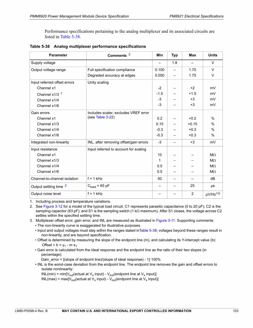
PMM8920 Power Management Module Device Specification PM8921 Electrical Specifications
LM80-P0598-4 Rev. B MAY CONTAIN U.S. AND INTERNATIONAL EXPORT CONTROLLED INFORMATION 103
Performance specifications pertaining to the analog multiplexer and its associated circuits are listed in Table 5-38.-
Table 5-38 Analog multiplexer performance specifications
Parameter Comments33 Min Typ Max Units
Supply voltage – 1.8 – V
Output voltage range Full specification compliance
Degraded accuracy at edges
0.100
0.050
–
–
1.70
1.75
V
V
Input referred offset errors
Channel x1
Channel x1/311
Channel x1/4
Channel x1/6
Unity scaling
-2
-1.5
-3
-3
–
–
–
–
+2
+1.5
+3
+3
mV
mV
mV
mV
Gain errors
Channel x1
Channel x1/3
Channel x1/4
Channel x1/6
Includes scaler; excludes VREF error (see Table 3-22) 0.2
0.15
-0.3
-0.3
–
–
–
–
+0.2
+0.15
+0.3
+0.3
%
%
%
%
Integrated non-linearity INL, after removing offset/gain errors -3 – +3 mV
Input resistance
Channel x1
Channel x1/3
Channel x1/4
Channel x1/6
Input referred to account for scaling
10
1
0.5
0.5
–
–
–
–
–
–
–
–
MMMM
Channel-to-channel isolation f = 1 kHz 50 – – dB
Output settling time22 Cload = 65 pF – – 25 µs
Output noise level f = 1 kHz – – 2 µV/Hz1/2
1. Including process and temperature variations.2. See Figure 3-12 for a model of the typical load circuit. C1 represents parasitic capacitance (0 to 20 pF); C2 is the
sampling capacitor (63 pF); and S1 is the sampling switch (1 k maximum). After S1 closes, the voltage across C2 settles within the specified settling time.
3. Multiplexer offset error, gain error, and INL are measured as illustrated in Figure 3-11. Supporting comments:• The non-linearity curve is exaggerated for illustrative purposes.• Input and output voltages must stay within the ranges stated inTable 5-38; voltages beyond these ranges result in
non-linearity, and are beyond specification.• Offset is determined by measuring the slope of the endpoint line (m), and calculating its Y-intercept value (b):
Offset = b = y1 - m·x1• Gain error is calculated from the ideal response and the endpoint line as the ratio of their two slopes (in
percentage):Gain_error = [(slope of endpoint line)/(slope of ideal response) - 1]·100%
• INL is the worst-case deviation from the endpoint line. The endpoint line removes the gain and offset errors to isolate nonlinearity:INL(min) = min[Vout(actual at Vx input) - Vout(endpoint line at Vx input)]INL(max) = max[Vout(actual at Vx input) - Vout(endpoint line at Vx input)]
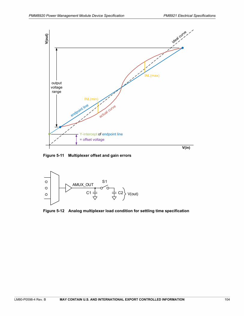
PMM8920 Power Management Module Device Specification PM8921 Electrical Specifications
LM80-P0598-4 Rev. B MAY CONTAIN U.S. AND INTERNATIONAL EXPORT CONTROLLED INFORMATION 104
Figure 5-11 Multiplexer offset and gain errors
Figure 5-12 Analog multiplexer load condition for settling time specification
output voltage range
Y-intercept of endpoint line
= offset voltage
endpoint line
actual c
urve
INL(min)
INL(max)
ideal curve
V(in)
V(o
ut)
S1AMUX_OUT
C2C1 V(out)

PMM8920 Power Management Module Device Specification PM8921 Electrical Specifications
LM80-P0598-4 Rev. B MAY CONTAIN U.S. AND INTERNATIONAL EXPORT CONTROLLED INFORMATION 105
5.7.2 HK/XO ADC circuit
The PMM8160 IC includes an analog-to-digital converter circuit that is shared by the housekeeping (HK) and 19.2 MHz crystal oscillator (XO) functions. A 2:1 analog multiplexer selects which source is applied to the ADC:
The HK source – the analog multiplexer output discussed in Section 5.7.1; or
The XO source – the thermistor network output that estimates the 19.2 MHz crystal temperature.
HK/XO ADC performance specifications are listed in Table 5-39.
AMUX input to ADC output end-to-end accuracy specifications are listed in Table 5-40.
Table 5-39 HK/XO ADC performance specifications
Parameter Comments Min Typ Max Units
Supply voltage – 1.8 – V
Resolution – – 15 bits
Analog input bandwidth – 100 – kHz
Sample rate XO/8 – 2.4 – MHz
Offset error -1 – +1 %
Gain error -1 – +1 %
INL 15 bit output -8 – +8 LSB
DNL 15 bit output -4 – +4 LSB
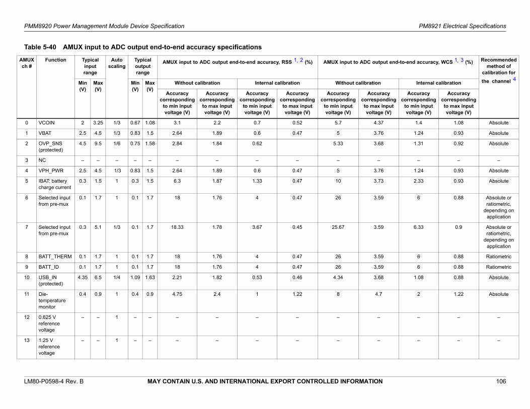
PMM8920 Power Management Module Device Specification PM8921 Electrical Specifications
LM80-P0598-4 Rev. B MAY CONTAIN U.S. AND INTERNATIONAL EXPORT CONTROLLED INFORMATION 106
Table 5-40 AMUX input to ADC output end-to-end accuracy specifications
AMUX ch #
Function Typical input range
Auto scaling
Typical output range
AMUX input to ADC output end-to-end accuracy, RSS11,22 (%) AMUX input to ADC output end-to-end accuracy, WCS 1,33 (%) Recommended method of
calibration for
the channel44Min (V)
Max (V)
Min (V)
Max (V)
Without calibration Internal calibration Without calibration Internal calibration
Accuracy corresponding
to min input voltage (V)
Accuracy corresponding to max input voltage (V)
Accuracy corresponding
to min input voltage (V)
Accuracy corresponding to max input voltage (V)
Accuracy corresponding
to min input voltage (V)
Accuracy corresponding to max input voltage (V)
Accuracy corresponding
to min input voltage (V)
Accuracy corresponding to max input voltage (V)
0 VCOIN 2 3.25 1/3 0.67 1.08 3.1 2.2 0.7 0.52 5.7 4.37 1.4 1.08 Absolute
1 VBAT 2.5 4.5 1/3 0.83 1.5 2.64 1.89 0.6 0.47 5 3.76 1.24 0.93 Absolute
2 OVP_SNS (protected)
4.5 9.5 1/6 0.75 1.58 2.84 1.84 0.62 5.33 3.68 1.31 0.92 Absolute
3 NC – – – – – – – – – – – – – –
4 VPH_PWR 2.5 4.5 1/3 0.83 1.5 2.64 1.89 0.6 0.47 5 3.76 1.24 0.93 Absolute
5 IBAT: battery charge current
0.3 1.5 1 0.3 1.5 6.3 1.87 1.33 0.47 10 3.73 2.33 0.93 Absolute
6 Selected input from pre-mux
0.1 1.7 1 0.1 1.7 18 1.76 4 0.47 26 3.59 6 0.88 Absolute or ratiometric,
depending on application
7 Selected input from pre-mux
0.3 5.1 1/3 0.1 1.7 18.33 1.78 3.67 0.45 25.67 3.59 6.33 0.9 Absolute or ratiometric,
depending on application
8 BATT_THERM 0.1 1.7 1 0.1 1.7 18 1.76 4 0.47 26 3.59 6 0.88 Ratiometric
9 BATT_ID 0.1 1.7 1 0.1 1.7 18 1.76 4 0.47 26 3.59 6 0.88 Ratiometric
10 USB_IN (protected)
4.35 6.5 1/4 1.09 1.63 2.21 1.82 0.53 0.46 4.34 3.68 1.08 0.88 Absolute
11 Die-temperature monitor
0.4 0.9 1 0.4 0.9 4.75 2.4 1 1.22 8 4.7 2 1.22 Absolute
12 0.625 V reference voltage
– – 1 – – – – – – – – – – –
13 1.25 V reference voltage
– – 1 – – – – – – – – – – –
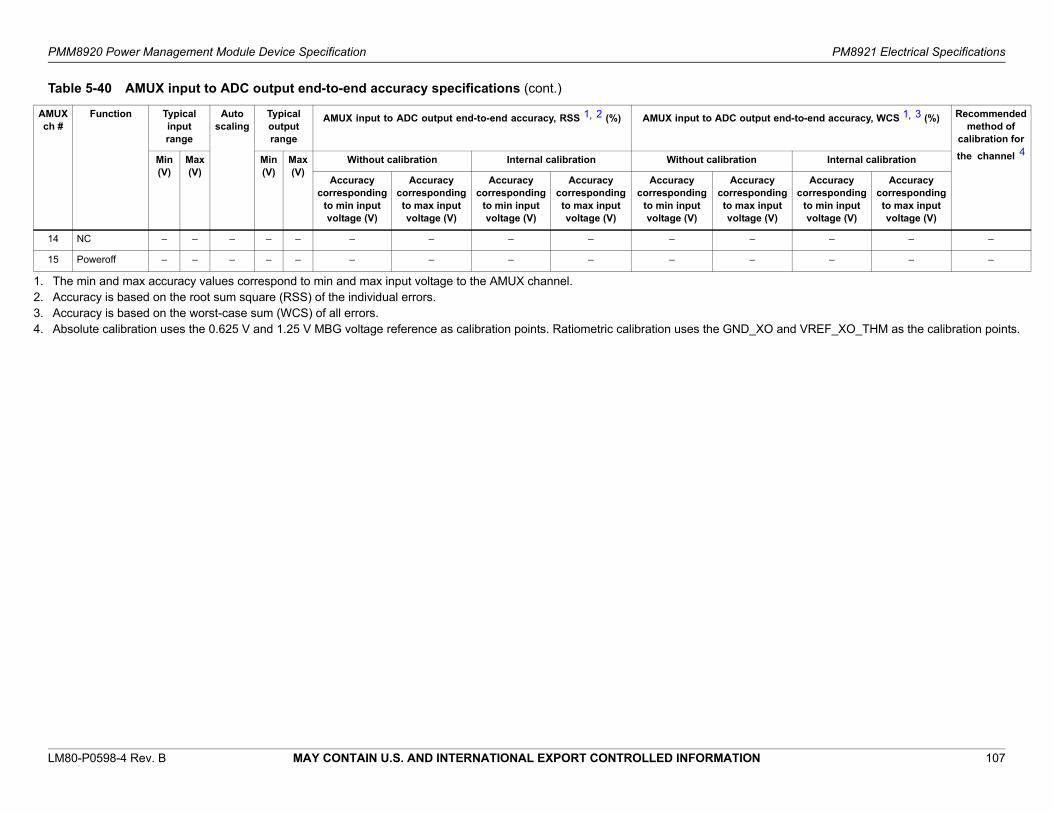
PMM8920 Power Management Module Device Specification PM8921 Electrical Specifications
LM80-P0598-4 Rev. B MAY CONTAIN U.S. AND INTERNATIONAL EXPORT CONTROLLED INFORMATION 107
14 NC – – – – – – – – – – – – – –
15 Poweroff – – – – – – – – – – – – – –
1. The min and max accuracy values correspond to min and max input voltage to the AMUX channel.2. Accuracy is based on the root sum square (RSS) of the individual errors.3. Accuracy is based on the worst-case sum (WCS) of all errors.4. Absolute calibration uses the 0.625 V and 1.25 V MBG voltage reference as calibration points. Ratiometric calibration uses the GND_XO and VREF_XO_THM as the calibration points.
Table 5-40 AMUX input to ADC output end-to-end accuracy specifications (cont.)
AMUX ch #
Function Typical input range
Auto scaling
Typical output range
AMUX input to ADC output end-to-end accuracy, RSS11,22 (%) AMUX input to ADC output end-to-end accuracy, WCS 1,33 (%) Recommended method of
calibration for
the channel44Min (V)
Max (V)
Min (V)
Max (V)
Without calibration Internal calibration Without calibration Internal calibration
Accuracy corresponding
to min input voltage (V)
Accuracy corresponding to max input voltage (V)
Accuracy corresponding
to min input voltage (V)
Accuracy corresponding to max input voltage (V)
Accuracy corresponding
to min input voltage (V)
Accuracy corresponding to max input voltage (V)
Accuracy corresponding
to min input voltage (V)
Accuracy corresponding to max input voltage (V)

PMM8920 Power Management Module Device Specification PM8921 Electrical Specifications
LM80-P0598-4 Rev. B MAY CONTAIN U.S. AND INTERNATIONAL EXPORT CONTROLLED INFORMATION 108
5.7.3 System clocks
The PMIC includes several clock circuits whose outputs are used for general housekeeping functions, and elsewhere within the device system. These circuits include a 19.2 MHz XO with multiple controllers and buffers, an MP3 clock output, 32.768 kHz crystal support, an RC oscillator, sleep clock outputs, and internal SMPL and SMPS clocks. Performance specifications for these functions are presented in the following subsections.
5.7.3.1 19.2 MHz XO circuits
An external crystal is supplemented by on-chip circuits to generate the desired 19.2 MHz reference signal. Using an external thermistor network, the on-chip ADC, and advanced temperature compensation software, the PMIC eliminates the large and expensive VCTCXO module required by previous generation chipsets. The XO circuits initialize and maintain valid pulse waveforms and measure time intervals for higher-level device functions. Multiple controllers manage the XO warmup and signal buffering, and generate the desired clock outputs (all derived from one source):
XO_OUT_A0
XO_OUT_A1
XO_OUT_A2
XO_OUT_D0
XO_OUT_D1
Since the different controllers and outputs are independent of each other, non-phone circuits can operate even while the phone’s baseband circuits are asleep and its RF circuits are powered down.
The PM8921 IC has built-in load capacitors on XTAL_19M_IN and XTAL_19M_OUT. A crystal that specifies 7 pF load caps is recommended because no external load capacitors will be required. This reduces the noise picked up from the GND plane.
The XTAL_19M_IN and XTAL_19M_OUT pins are incapable of driving a load – the oscillator will be significantly disrupted if either pin is externally loaded.
As discussed in Section 5.7.3.5, an RC oscillator is used to drive some clock circuits until the XO source is established.

PMM8920 Power Management Module Device Specification PM8921 Electrical Specifications
LM80-P0598-4 Rev. B MAY CONTAIN U.S. AND INTERNATIONAL EXPORT CONTROLLED INFORMATION 109
Table 5-41 Specifications for XO_OUT_D0 and XO_OUT_D1
Parameter Comments Min Typ Max Unit
Frequency Set by external crystal – 19.2 – MHz
Output duty cycle11 46 50 60 %
USB 2.0 jitter
0.5 MHz – 2 MHz22
> 2 MHz
Specified values are peak-to-peak period jitter –
–
–
–
50
100
ps
ps
Startup time33 – – 6 ms
Current consumption 0.94 0.98 1.0 mA
Supply voltage 1.782 1.80 1.818 V
Buffer output impedance44
at 1x drive strength
at 2x drive strength
at 3x drive strength
at 4x drive strength
54
30
21
17
80
42
30
22
122
64
44
35
Ω / mA
Ω / mA
Ω / mA
Ω / mA
1. Duty cycle is defined as the first pulse duty cycle that meets the overall duty cycle specification.2. USB period jitter can be calculated by 14 · Jitterrms based on the 10-12 BER requirement.3. When the warmup time enhancement feature is enabled, this can be reduced to 3.5 ms (to be finalized after
analysis of more characterization data).4. Output impedance at each drive strength varies 30% over corners. Current drive capabilities included to meet
VOH = 0.65 · VDD and VOL = 0.35 · VDD.
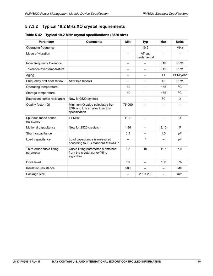
PMM8920 Power Management Module Device Specification PM8921 Electrical Specifications
LM80-P0598-4 Rev. B MAY CONTAIN U.S. AND INTERNATIONAL EXPORT CONTROLLED INFORMATION 110
5.7.3.2 Typical 19.2 MHz XO crystal requirements
Table 5-42 Typical 19.2 MHz crystal specifications (2520 size)
Parameter Comments Min Typ Max Units
Operating frequency – 19.2 – MHz
Mode of vibration – AT-cut fundamental
– –
Initial frequency tolerance – – ±10 PPM
Tolerance over temperature – – ±12 PPM
Aging – – ±1 PPM/year
Frequency drift after reflow After two reflows – – ±2 PPM
Operating temperature -30 – +85 ⁰C
Storage temperature -40 – +85 ⁰C
Equivalent series resistance New for2520 crystals – 80
Quality factor (Q) Minimum Q value calculated from ESR and L is smaller than this specification
75,000 – – –
Spurious mode series resistance
±1 MHz 1100 – –
Motional capacitance New for 2520 crystals 1.80 – 3.10 fF
Shunt capacitance 0.3 – 1.3 pF
Load capacitance Load capacitance is measured according to IEC standard #60444-7
– 7 – pF
Third-order curve fitting parameter
Curve fitting parameter is obtained from the crystal curve-fitting algorithm
8.5 10 11.5 e-5
Drive level 10 – 100 µW
Insulation resistance 500 – – M
Package size – 2.5 × 2.0 – mm

PMM8920 Power Management Module Device Specification PM8921 Electrical Specifications
LM80-P0598-4 Rev. B MAY CONTAIN U.S. AND INTERNATIONAL EXPORT CONTROLLED INFORMATION 111
Table 5-43 Specifications for XO_OUT_A0, XO_OUT_A1, and XO_OUT_A2
Parameter Comments Min Typ Max Unit
Frequency Set by external crystal – 19.2 – MHz
Duty cycle 40 50.0 60.0 %
Startup time11 – 6 – ms
Current consumption22
HPM
NPM
LPM
0.89
1.11
1.23
1.14
1.23
1.39
1.38
1.52
1.74
mA
mA
mA
Output voltage swing 1.2 – 1.8 V
Buffer output impedance33
at 1x drive strength
at 2x drive strength
at 3x drive strength
at 4x drive strength
54
30
21
17
80
42
30
22
122
64
44
35
Ω / mA
Ω / mA
Ω / mA
Ω / mA
Phase noise in LPM
at 10 Hz
at 100 Hz
at 1 kHz
at 10 kHz
at 100 kHz
at 1 MHz
–
–
–
–
–
–
–
–
–
–
–
–
-86
-110
-124
-134
-140
-137
dBc/Hz
dBc/Hz
dBc/Hz
dBc/Hz
dBc/Hz
dBc/Hz
Phase noise in NPM
at 10 Hz
at 100 Hz
at 1 kHz
at 10 kHz
at 100 kHz
at 1 MHz
–
–
–
–
–
–
–
–
–
–
–
–
-86
-116
-134
-144
-144
-144
dBc/Hz
dBc/Hz
dBc/Hz
dBc/Hz
dBc/Hz
dBc/Hz
Phase noise in HPM
at 10 Hz
at 100 Hz
at 1 kHz
at 10 kHz
at 100 kHz
at 1 MHz
–
–
–
–
–
–
–
–
–
–
–
–
-86
-116
-134
-144
-148
-150
dBc/Hz
dBc/Hz
dBc/Hz
dBc/Hz
dBc/Hz
dBc/Hz
1. The startup time corresponds to the time taken by the buffer to output the first valid pulse that meets the overall duty-cycle specification. When the warmup time enhancement feature is enabled, this can be reduced to 3.5 ms.
2. Includes 15 pF load cap, output swing = 1.8 V.3. Output impedance at each drive strength varies 30% over corners. Current drive capabilities included to meet
VOH = 0.65 · VDD and VOL = 0.35 · VDD.

PMM8920 Power Management Module Device Specification PM8921 Electrical Specifications
LM80-P0598-4 Rev. B MAY CONTAIN U.S. AND INTERNATIONAL EXPORT CONTROLLED INFORMATION 112
5.7.3.3 MP3 clock
One GPIO can be configured as a 2.4 MHz clock output to support MP3 in a low-power mode. This clock is a divided down version of the 19.2 MHz XO signal, so its most critical performance features are defined within the XO tables (Section 5.7.3.1). Output characteristics (voltage levels, drive strength, etc.) are defined in Section 5.4
5.7.3.4 32 kHz oscillator
The following are three options for implementing the 32 kHz oscillator:
Using the XO signal (19.2 MHz)
An external 32.768 kHz crystal oscillator
An external oscillator module
Whichever method is used, this oscillator signal is the primary sleep clock source. In all cases, neither the XTAL_32K_IN nor the XTAL_32K_OUT pins are capable of driving a load – the oscillator will be significantly disrupted if either pin is loaded.
The PMIC includes a circuit that continually monitors this oscillation. If the circuit is enabled but stops oscillating, the device automatically switches to the internal RC oscillator and generates an interrupt.
Performance specifications pertaining to the 32 kHz oscillator are listed in Table 5-44
Table 5-44 Typical 32 kHz crystal specification
Parameter Comments Min Typ Max Unit
Nominal oscillation frequency F – 32.768 – kHz
Load capacitance CL 7 – 12.5 pF
Frequency tolerance ΔF/F -100 100 ppm
Drive level P – 0.1 1 µW
Aging first year ΔF/F -3 – 3 ppm
Series resistance Rs – 50 80 kΩ
Motional capacitance C1 – 2.1 – fF
Static capacitance C0 – 0.9 – pF

PMM8920 Power Management Module Device Specification PM8921 Electrical Specifications
LM80-P0598-4 Rev. B MAY CONTAIN U.S. AND INTERNATIONAL EXPORT CONTROLLED INFORMATION 113
5.7.3.5 RC oscillator
As mentioned in previous sections, the PMIC includes an on-chip RC oscillator that is used during startup and as a backup to the 32 kHz oscillator. Pertinent performance specifications are listed in Table 5-45.
5.7.3.6 Sleep clock
The sleep clock is generated one of three ways:
Using the 19.2 MHz XO circuit and dividing its output by 586 to create a 32.7645 kHz signal – this method supports all normal operating modes.
Using the 32.768 kHz crystal and supporting PMIC circuits – this method supports all normal operating modes.
Using the on-chip 19.2 MHz RC oscillator and divide-by-586 to create a coarse 32 kHz signal – this method is only used during startup and if the 32.768 kHz XTAL source fails.
The PMIC sleep clock output is routed to the APQ or QSC device circuits using the SLEEP_CLK0 pin. It is also available for other applications via GPIO_43 and GPIO_44 when configured properly (as SLEEP_CLK1 and SLEEP_CLK2, respectively).
These clock outputs are derived from other sources specified earlier:
19.2 MHz XO circuits (Section 5.7.3.1)
32.768 kHz XTAL oscillator (Section 5.7.3.4)
19.2 MHz RC oscillator (Section 5.7.3.5)
Output characteristics (voltage levels, drive strength, etc.) are defined in Section 5.4.
5.7.4 Realtime clock
The realtime clock functions are implemented by a 32-bit realtime counter and one 32-bit alarm, both configurable in one-second increments. The primary input to the RTC circuits is the 32.768 kHz clock from the XTAL oscillator. Even when the phone is off, the oscillator and RTC continue to run off the main battery.
If the main battery is present and an SMPL event occurs, RTC contents are corrupted. As power is restored, the RTC pauses and skips a few seconds. The phone must reacquire system time from the network to resume the usual RTC accuracy. Similarly, if the main battery is not present and the voltage at VCOIN drops too low, RTC contents are again corrupted. In either case, the RTC reset interrupt is generated. A different interrupt is generated if the oscillator stops, also causing RTC errors.
Table 5-45 RC oscillator performance specifications
Parameter Comments Min Typ Max Units
Oscillation frequency 14 19.2 24 MHz
Duty cycle 30 50 70 %
Divider in SLEEP_CLK path – 586 – –

PMM8920 Power Management Module Device Specification PM8921 Electrical Specifications
LM80-P0598-4 Rev. B MAY CONTAIN U.S. AND INTERNATIONAL EXPORT CONTROLLED INFORMATION 114
The RTC is an entirely embedded function, without the external I/Os needing to be specified. All its controls and output data are accessed internally, and its accuracy depends entirely on the oscillator source being used – defined elsewhere. Therefore, no RTC performance parameters need to be defined here.
Table 5-46 lists RTC performance specifications.
5.7.5 Overtemperature protection (smart thermal control)
The PMIC includes overtemperature protection in stages, depending upon the level of urgency as the die temperature rises:
Stage 0 – normal operating conditions (less than 110°C).
Stage 1 – 110°C to 130°C; an interrupt is sent to the APQ or QSC device without shutting down any PMIC circuits.
Stage 2 – 130°C to 150°C; an interrupt is sent to the APQ or QSC device and high-current drivers (backlight drivers, LED drivers, etc.) are shut down.
Stage 3 – greater than 150°C; an interrupt is sent to the APQ or QSC device and the PMIC is completely shut down.
Temperature hysteresis is incorporated such that the die temperature must cool significantly before the device can be powered on again. If any start signals are present while at Stage 3, they are ignored until Stage 0 is reached. When the device cools enough to reach Stage 0 and a start signal is present, the PMIC will power up immediately.
Table 5-46 RTC performance specs when using Cal RC, XO/586 and 32 kHz oscillator
Parameter Comments23 Min Typ Max Unit
Tuning resolution With known calibrated source – 3.05 – ppm
Tuning range -192 – 192 ppm
Accuracy (phone off)
Cal RC with valid phone battery
Cal RC with qualified coin-cell or super capacitor
32 kHz XTAL11
19.2 MHz XO (Cal RC in state S4)
–
–
–
–
–
–
–
–
200
200
100
24
ppm
ppm
ppm
ppm
Accuracy (phone on)
19.2 MHz XO
32 kHz XTAL Appendix 2
–
–
–
–
24
100
ppm
ppm
SMPL
XO/586 used as SMPL source
RC/586 used as SMPL source
4.7 µF used on VCOIN
2
2
–
–
–
–
s
s
1. RTC accuracy depends on the frequency accuracy of the external 32 kHz crystal.2. Valid over the temperature range of -30 °C to 60 °C.

PMM8920 Power Management Module Device Specification PM8921 Electrical Specifications
LM80-P0598-4 Rev. B MAY CONTAIN U.S. AND INTERNATIONAL EXPORT CONTROLLED INFORMATION 115
5.8 User interfaces
In addition to housekeeping functions, the PMIC also includes these circuits in support of common device-level user interfaces: an 8-channel light pulse generator; current drivers (and control signals for external current drivers); vibration motor driver; one-touch headset controls and microphone bias outputs; external switch detectors; an 8 × 8 keypad interface; enable; joystick interface.
All parameters associated with user interface functions are specified in the following subsections.
5.8.1 Light pulse generator
The PMIC includes a light pulse generator (LPG) circuit that can be used to control fun lights to flash multiple colors in a variety of patterns – from a constant torch mode to a user-programmed pattern. The pattern timing is generated by pulse-width modulator (PWM) circuits.
Since this function is entirely embedded within the PMIC, performance specifications are not appropriate.
The LPG outputs can be used to control the on-chip current drivers, or to control external current drivers through up to three GPIOs (discussed in Section 5.8.2).
The LPG channels are assigned as follows:
Channel Usage
1 GPIO24
2 GPIO25
3 GPIO26
4 KYPD_DRV
5 LED_DRV0
6 LED_DRV1
7 LED_DRV2
8 VIB_DRV_N

PMM8920 Power Management Module Device Specification PM8921 Electrical Specifications
LM80-P0598-4 Rev. B MAY CONTAIN U.S. AND INTERNATIONAL EXPORT CONTROLLED INFORMATION 116
5.8.2 LPG controllers (digital driver outputs)
Up to three GPIOs can be configured as LPG controllers: GPIO_26 = LPG_DRV3, GPIO_25 = LPG_DRV2, and GPIO_24 = LPG_DRV1. Output characteristics (voltage levels, drive strength, etc.) were defined inSection 5.4.
The PWM frequency is
Fpwm = Fclk/((2PwmSize)*(2M)*PreDiv)
where
Fclk = 19.2 MHz, 32 kHz, or 1 kHz
PwmSize = 6 or 9
M = 0, 1,..., or 7
PreDiv = 2, 3, 5, or 6
The PWM duty cycle is (PWM value)/512 in 9-bit mode and (PWM value[5:0])/64 in 6-bit mode.
5.8.3 Current drivers
Three types of current drivers are available:
A keypad driver that can operate off +5 V with programmable settings to 300 mA
Three LED drivers to operate off VDD with programmable settings to 40 mA
One automatic trickle charging indicator that operates off VDD at a fixed 5 mA
Current driver performance specifications are listed in Table 5-47.
Table 5-47 Current driver performance specifications
Parameter Comments Min Typ Max Units
Common to all drivers
Current accuracy Any programmed value -20 – +20 %
Headroom11 Any programmed value 500 – – mV
Keypad driver
Output current Programmable in 20 mA increments 0 – 300 mA
Power supply voltage – 5.00 5.25 V
Power supply current
Normal operation
Off, from supply voltage
Off, at driver output pin
At max output current –
–
–
200
1
250
100
A
nA
nA
LED current drivers
Output current Programmable in 2 mA increments 0 – 40 mA
Power supply voltage – VDD – V

PMM8920 Power Management Module Device Specification PM8921 Electrical Specifications
LM80-P0598-4 Rev. B MAY CONTAIN U.S. AND INTERNATIONAL EXPORT CONTROLLED INFORMATION 117
Figure 5-13 KPD_DRV chart
Power supply current
Normal operation
Off, from supply voltage
Off, at driver output pin –
65
20
1
80
100
50
A
nA
nA
ATC current driver (shared with LED_DRV0_N)
Output current (fixed) – 5 – mA
Current accuracy Any programmed value -30 – +30 %
Headroom 1 Any programmed value 800 – – mV
1. Lowest output voltage while still meeting the current accuracy specification.
Table 5-47 Current driver performance specifications (cont.)
Parameter Comments Min Typ Max Units
5
55
105
155
205
255
305
355
0.1 0.15 0.2 0.25 0.3 0.4 0.5 0.6 0.7
Cur
rent
dro
p (m
A)
KPD_DRV output (V)
KPD_DRV Headroom Data at Irated = 300mA (Temp = 25C)
Device 1
Device 2
Device 3
Device 4
Device 5

PMM8920 Power Management Module Device Specification PM8921 Electrical Specifications
LM80-P0598-4 Rev. B MAY CONTAIN U.S. AND INTERNATIONAL EXPORT CONTROLLED INFORMATION 118
5.8.4 Vibration motor driver
The PMIC supports silent incoming call alarms with its vibration motor driver. The vibration driver is a programmable voltage output that is referenced to VDD; when off, its output voltage is VDD. The motor is connected between VDD and the VIB_DRV_N pin.
Performance specifications for the vibration motor driver circuit are listed in Table 5-48.
5.8.5 One-touch headset control and MIC bias
The headset send/end detect (HSED) circuits communicate the wired headset’s send/end button state to the APQ or QSC device through an interrupt. This design allows for simultaneous detection of both normally open (NO) and normally closed (NC) microphone switch types, or allows both a NO button press/release and a headset insertion/removal to be detected.
Three pins support this function: HSED_BIAS1, HSED_BIAS2, and HSED_BIAS3. In addition to the detection capabilities, each pin also provides the bias voltage for a microphone.
Pertinent performance specifications are listed in Table 5-49.
Table 5-48 Vibration motor driver performance specifications
Parameter Comments Min Typ Max Units
Output voltage (Vm) error11
Relative error
Absolute error
VDD > 3.2 V; Im = 0 to 175 mA; Vm setting = 1.2 to 3.1 V
Total error = relative + absolute
-6
-60
–
–
+6
+60
%
mV
Headroom22 Im = 175 mA – – 200 mV
Short circuit current VIB_DRV_N = VDD 225 – 600 mA
1. The vibration motor driver circuit is a low-side driver. The motor is connected directly to VDD, and the voltage across the motor is Vm = VDD - Vout, where Vout is the PMIC voltage at VIB_DRV_N.
2. Adjust the programmed voltage until the lowest motor voltage occurs while still meeting the voltage accuracy specification. This lowest motor voltage (Vm = VDD - Vout) is the headroom.
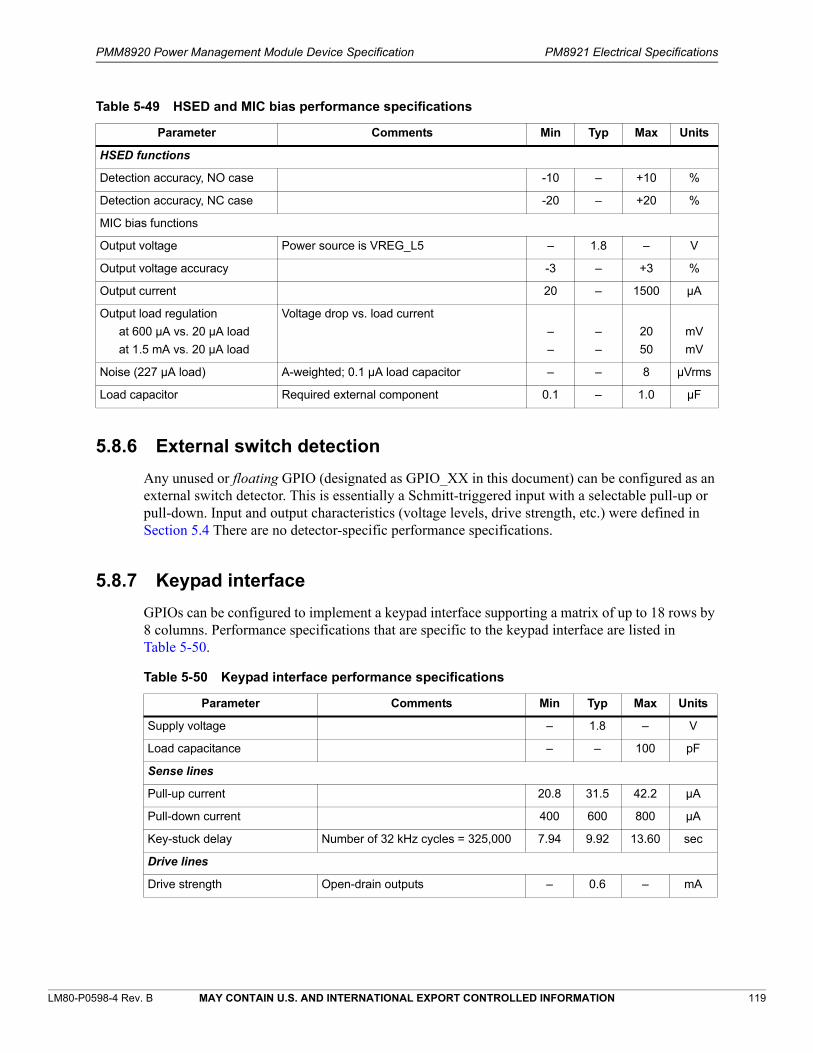
PMM8920 Power Management Module Device Specification PM8921 Electrical Specifications
LM80-P0598-4 Rev. B MAY CONTAIN U.S. AND INTERNATIONAL EXPORT CONTROLLED INFORMATION 119
5.8.6 External switch detection
Any unused or floating GPIO (designated as GPIO_XX in this document) can be configured as an external switch detector. This is essentially a Schmitt-triggered input with a selectable pull-up or pull-down. Input and output characteristics (voltage levels, drive strength, etc.) were defined in Section 5.4 There are no detector-specific performance specifications.
5.8.7 Keypad interface
GPIOs can be configured to implement a keypad interface supporting a matrix of up to 18 rows by 8 columns. Performance specifications that are specific to the keypad interface are listed in Table 5-50.
Table 5-49 HSED and MIC bias performance specifications
Parameter Comments Min Typ Max Units
HSED functions
Detection accuracy, NO case -10 – +10 %
Detection accuracy, NC case -20 – +20 %
MIC bias functions
Output voltage Power source is VREG_L5 – 1.8 – V
Output voltage accuracy -3 – +3 %
Output current 20 – 1500 µA
Output load regulation
at 600 µA vs. 20 µA load
at 1.5 mA vs. 20 µA load
Voltage drop vs. load current
–
–
–
–
20
50
mV
mV
Noise (227 µA load) A-weighted; 0.1 µA load capacitor – – 8 µVrms
Load capacitor Required external component 0.1 – 1.0 µF
Table 5-50 Keypad interface performance specifications
Parameter Comments Min Typ Max Units
Supply voltage – 1.8 – V
Load capacitance – – 100 pF
Sense lines
Pull-up current 20.8 31.5 42.2 µA
Pull-down current 400 600 800 µA
Key-stuck delay Number of 32 kHz cycles = 325,000 7.94 9.92 13.60 sec
Drive lines
Drive strength Open-drain outputs – 0.6 – mA
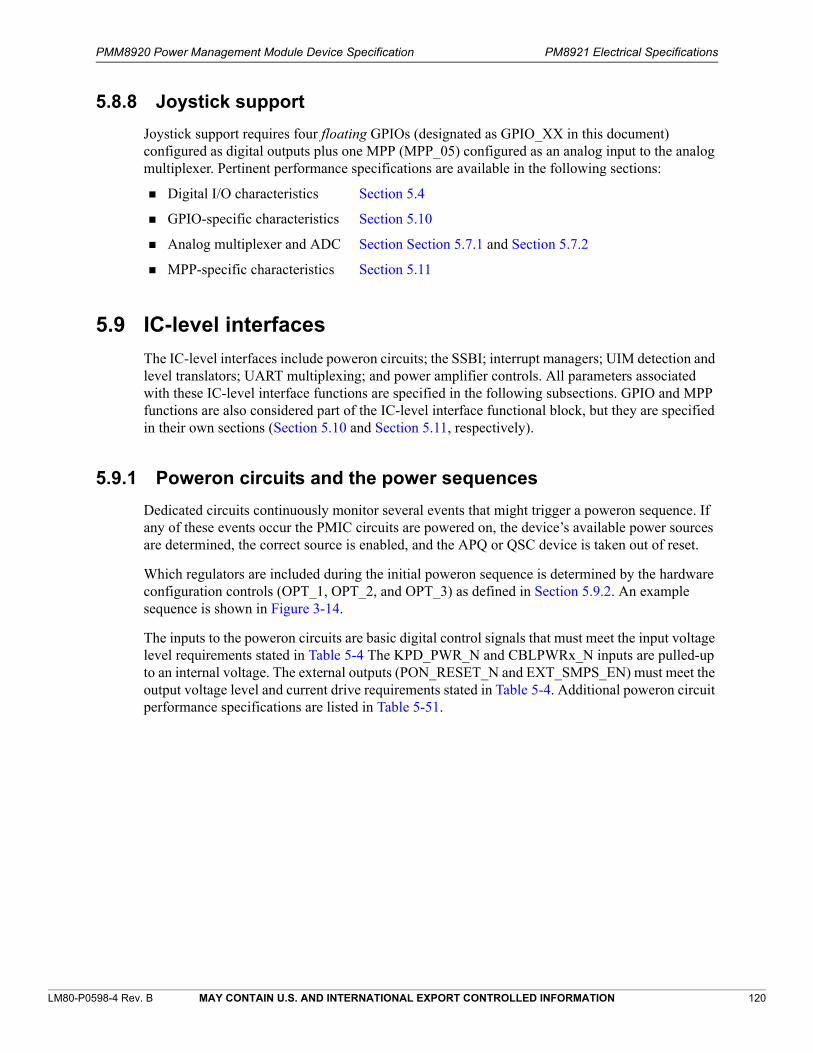
PMM8920 Power Management Module Device Specification PM8921 Electrical Specifications
LM80-P0598-4 Rev. B MAY CONTAIN U.S. AND INTERNATIONAL EXPORT CONTROLLED INFORMATION 120
5.8.8 Joystick support
Joystick support requires four floating GPIOs (designated as GPIO_XX in this document) configured as digital outputs plus one MPP (MPP_05) configured as an analog input to the analog multiplexer. Pertinent performance specifications are available in the following sections:
Digital I/O characteristics Section 5.4
GPIO-specific characteristics Section 5.10
Analog multiplexer and ADC Section Section 5.7.1 and Section 5.7.2
MPP-specific characteristics Section 5.11
5.9 IC-level interfaces
The IC-level interfaces include poweron circuits; the SSBI; interrupt managers; UIM detection and level translators; UART multiplexing; and power amplifier controls. All parameters associated with these IC-level interface functions are specified in the following subsections. GPIO and MPP functions are also considered part of the IC-level interface functional block, but they are specified in their own sections (Section 5.10 and Section 5.11, respectively).
5.9.1 Poweron circuits and the power sequences
Dedicated circuits continuously monitor several events that might trigger a poweron sequence. If any of these events occur the PMIC circuits are powered on, the device’s available power sources are determined, the correct source is enabled, and the APQ or QSC device is taken out of reset.
Which regulators are included during the initial poweron sequence is determined by the hardware configuration controls (OPT_1, OPT_2, and OPT_3) as defined in Section 5.9.2. An example sequence is shown in Figure 3-14.
The inputs to the poweron circuits are basic digital control signals that must meet the input voltage level requirements stated in Table 5-4 The KPD_PWR_N and CBLPWRx_N inputs are pulled-up to an internal voltage. The external outputs (PON_RESET_N and EXT_SMPS_EN) must meet the output voltage level and current drive requirements stated in Table 5-4. Additional poweron circuit performance specifications are listed in Table 5-51.

PMM8920 Power Management Module Device Specification PM8921 Electrical Specifications
LM80-P0598-4 Rev. B MAY CONTAIN U.S. AND INTERNATIONAL EXPORT CONTROLLED INFORMATION 121
Table 5-51 Poweron circuit performance specifications
Parameter Comments Min Typ Max Units
Internal pull-up resistor11
KPD_PWR_N and CBLPWRx_N pins
RESIN_N pin
150
32
200
40
250
48
k
k
KPDPWR_N pull up volt – 1.8 – V
CBLPWR_N pull up volt – 0.8 – V
Sequence time intervals22
t(reg1)
t(reg)
t(settle)
t(xo)
t(reset1)
t(pshold)
t(reset0)
t(reg0)
t(psholdoff)
Poweron event to first regulator on44
Time for reg to settle before next enable
Regulator settling time55
XO regulator enable to valid XO pulses
Last regulator on to PON_RESET_N = H
PS_HOLD timeout66
PON_RESET_N = L to Group 0 regulators off
Time between regulator group shutdowns
Delay from PSHOLD drop to PON_RESET_N
–
100
20
–
10
133
6.7
0.6
–
165
128
–
15
20
200
10.0
1
60
–
500
500
–
30
300
15
1.4
90
ms
µs
µs
ms
ms
ms
ms
ms
µs
Regulator accuracy To continue poweron sequence 4 7 9 %
Debounce timer33 16 – 10256 ms
1. This internal resistor is pulled up directly to an internal voltage net (dVdd).2. All time intervals are derived from the divided-down XO clock source (32.7645 kHz typical); their tolerances are set
accordingly. See Figure 3-14 for further discussion.3. This is the delay between a triggering event (such as a keypad press) and the corresponding interrupt. The value is
programmable.4. The first regulator poweron time t(reg1) depends on the bandgap reference decoupling capacitor at REF_BYP. The
specified value is based on 0.1 F. This time includes the default 16 ms keypad debounce, the 64 ms UVLO debounce timers, and 80 ms for BMS-related measurements. This is in addition to the default 6 ms of poweron delay. If these debounce timers are increased, then the t(reg1) value will also increase.
5. Each regulator will settle to within its stated regulator accuracy within the stated regulator settling time. The regulators are turned on and off in the orders illustrated in Figure 3-14. This assumes nominal capacitance on the regulator output. Increasing the capacitance on the rail will directly impact settling time.
6. This is the time range where PS_HOLD must go high or the t(pshold) timer will time out and the device will power down. It is acceptable for PS_HOLD to be high any time during the poweron sequence as long as it goes high before the t(pshold) timer expires.
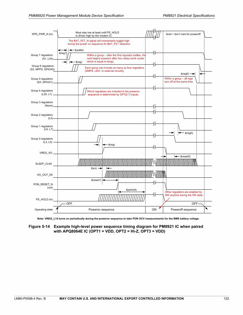
PMM8920 Power Management Module Device Specification PM8921 Electrical Specifications
LM80-P0598-4 Rev. B MAY CONTAIN U.S. AND INTERNATIONAL EXPORT CONTROLLED INFORMATION 122
Figure 5-14 Example high-level power sequence timing diagram for PM8921 IC when paired with APQ8064E IC (OPT1 = VDD, OPT2 = Hi-Z, OPT3 = VDD)
Other regulators are enabled bySW anytime during the ON state.
PON_RESET_N(out)
PS_HOLD (in)
Operating state Poweron sequence ON Poweroff sequence
Must stay low at least until PS_HOLDis driven high by the modem IC. level = don’t care for poweroff
t(reg1)
SLEEP_CLK0
XO_OUT_D0
KPD_PWR_N (in)
OFF
Group 7 regulators
Group 5 regulators
VREG_XO
t(settle)
t(reg)
t(xo)
t(reset1)
t(pshold)
t(reset0)
t(reg0)
t(reg0)
Which regulators are included in the poweronsequence is determined by OPT[3:1] inputs.
Group 4 regulators
Group 3 regulators
Group 2 regulators
Within a group – after the first regulator settles, thenext begins poweron after four sleep-clock cycleswhich is equal to t(reg).
Within a group – all regsturn off at the same time.
Group 1 regulators
Group 0 regulators
t(reg)
OFF
Group 6 regulatorsEach group can include as many as four regulators(SMPS, LDO, or external circuits).
(S1, L24)
(S3, MPP5, GPIO40)
(S4, GPIO41)
(L25, L1)
(None)
(L4)
(L6, L7)
(L3, L5)
Note: VREG_L14 turns on periodically during the poweron sequence to take PON OCV measurements for the BMS battery voltage.
The BAT_FET_N signal will momentarily toggle highduring the power on sequence for BAT_FET detection

PMM8920 Power Management Module Device Specification PM8921 Electrical Specifications
LM80-P0598-4 Rev. B MAY CONTAIN U.S. AND INTERNATIONAL EXPORT CONTROLLED INFORMATION 123
5.9.2 SSBI and the interrupt managers
The SSBI is a bidirectional digital signal that meets the voltage and current level requirements stated in Table 5-4.
Three interrupt managers support ADC and USB functions, and report on numerous conditions, conveying realtime and latched status signals to the APQ or QSC device, thereby supporting the interrupt processing of those devices. The interrupt managers are mostly embedded functions; the three interrupt outputs meet the voltage and current level requirements stated in Table 5-4. Most other control and status data are accessed via SSBI, supplemented by dedicated, realtime controls where needed.
Table 5-52 lists the PM8921 interrupts and their functions.
Table 5-52 PM8921 interrupt list
Interrupt name11 Function
Charger-related interrupts
USBIN_VALID USBIN voltage is within the valid range.
USBIN_OV USBIN > Vmax.
BATT_INSERTED Battery replaced in the system; battery thermistor monitor is disabled or VTHERM voltage is below the open circuit threshold (95%).
VBATDET_LOW VBAT < VBATDET, as measured by the VBATDET comparator.
USBIN_UV USBIN < Vmin.
VBAT_OV VBAT > VBATDET for at least 1 second.
CHGWDOG Charging watchdog timer has expired, and charging has been stopped.
VCP VDD collapse protection has been triggered.
ATCDONE Auto trickle charging is complete.
ATCFAIL Auto trickle charging has failed.
CHGDONE Autonomous charging is complete.
CHGFAIL Auto charging has failed. The max fast-charging time has been exceeded without ever reaching the termination current.
CHGSTATE The charger state machine has changed states.
LOOP_CHANGE The SMBC buck transitions between control loops (VDD/IBAT/IUSB/VIN)
FASTCHG The charger is fast charging.
TRKLCHG The linear trickle charger is on during software-controlled charging.
BATT_REMOVED The battery thermistor monitor is enabled, and the thermistor is either shorted or open.
BATTTEMP_HOT The battery thermistor monitor is enabled, and the temperature is too hot for charging (> 40°C).
CHGHOT The charger temperature exceeds a set limit.
BATTTEMP_COLD The battery thermistor monitor is enabled, and the temperature is too cold for charging (< 0°C).
CHG_GONE Charger removal has been detected.

PMM8920 Power Management Module Device Specification PM8921 Electrical Specifications
LM80-P0598-4 Rev. B MAY CONTAIN U.S. AND INTERNATIONAL EXPORT CONTROLLED INFORMATION 124
BAT_TEMP_OK The battery temperature is in the normal range.
COARSE_DET_LOW This is generated if both the DC-path and USB-path input voltages are less than the coarse-detect falling threshold (~0.7 V) for at least 1 second.
VDD_LOOP Interrupts when the SMBC buck transitions to the voltage regulation loop.
VREG_OV This is generated if the SMBC buck detects an overshoot voltage greater than 5% of the programmed VDD_MAX value.
VBAT VBAT – battery status change: 1 = battery voltage has stayed above BAT_UPR_THRESH threshold or below BAT_LWR_THRESH threshold for longer than the BAT_ALRM_HYST delay timer setting.
VBATDET VBATDET – threshold reached: 1 = VBAT has reached the top-off threshold setting (VBATDET register setting).
BATFET BATFET is closed.
OVPSNS_VALID OVPSNS is within the valid range.
OVPSNS_OV OVPSNS > Vmax.
OVPSNS_UV OVPSNS < Vmin.
Poweron/off and RTC interrupts
RTCALRM The RTC alarm has been triggered.
OSCHALT_32k The 32 kHz XTAL oscillation has stopped.
WDOG_BARK The hardware watchdog bark interrupt has occurred.
SMPL An SMPL event has occurred.
CABLE A cable poweron event has occurred.
OVERTEMP Overtemperature shutdown has occurred.
WDOG A watchdog timeout event has occurred.
KPDPWR A keypad poweron event has occurred.
Temperature and power-key interrupts
TEMPSTAT Indicates a temperature status change.
OSCHALT_19M2 19.2 MHz XO has stopped oscillating.
RTC_1Hz The RTC 1 Hz clock interrupt.
RESOUT The reset pin requests powerdown.
KPDPWRON The keypad power key has been pressed.
KPDPWROFF The keypad power key has been released.
USB_ID_INT The USB_ID state interrupt.
OTG_OCP USB OTG switch OCP has been tripped.
ADC/headset/UICC interrupts (not used on the APQ8064E chipset)
UICC1_SEQ_OFF The UICC1 has been sequenced off.
UICC2_SEQ_OFF The UICC2 has been sequenced off.
HSED_NO_2 Headset send/end detect 2 NO output.
Table 5-52 PM8921 interrupt list (cont.)
Interrupt name11 Function
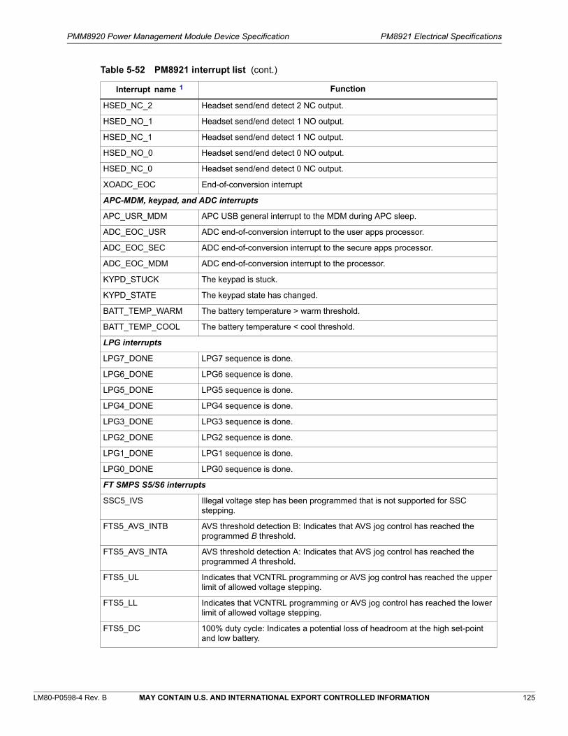
PMM8920 Power Management Module Device Specification PM8921 Electrical Specifications
LM80-P0598-4 Rev. B MAY CONTAIN U.S. AND INTERNATIONAL EXPORT CONTROLLED INFORMATION 125
HSED_NC_2 Headset send/end detect 2 NC output.
HSED_NO_1 Headset send/end detect 1 NO output.
HSED_NC_1 Headset send/end detect 1 NC output.
HSED_NO_0 Headset send/end detect 0 NO output.
HSED_NC_0 Headset send/end detect 0 NC output.
XOADC_EOC End-of-conversion interrupt
APC-MDM, keypad, and ADC interrupts
APC_USR_MDM APC USB general interrupt to the MDM during APC sleep.
ADC_EOC_USR ADC end-of-conversion interrupt to the user apps processor.
ADC_EOC_SEC ADC end-of-conversion interrupt to the secure apps processor.
ADC_EOC_MDM ADC end-of-conversion interrupt to the processor.
KYPD_STUCK The keypad is stuck.
KYPD_STATE The keypad state has changed.
BATT_TEMP_WARM The battery temperature > warm threshold.
BATT_TEMP_COOL The battery temperature < cool threshold.
LPG interrupts
LPG7_DONE LPG7 sequence is done.
LPG6_DONE LPG6 sequence is done.
LPG5_DONE LPG5 sequence is done.
LPG4_DONE LPG4 sequence is done.
LPG3_DONE LPG3 sequence is done.
LPG2_DONE LPG2 sequence is done.
LPG1_DONE LPG1 sequence is done.
LPG0_DONE LPG0 sequence is done.
FT SMPS S5/S6 interrupts
SSC5_IVS Illegal voltage step has been programmed that is not supported for SSC stepping.
FTS5_AVS_INTB AVS threshold detection B: Indicates that AVS jog control has reached the programmed B threshold.
FTS5_AVS_INTA AVS threshold detection A: Indicates that AVS jog control has reached the programmed A threshold.
FTS5_UL Indicates that VCNTRL programming or AVS jog control has reached the upper limit of allowed voltage stepping.
FTS5_LL Indicates that VCNTRL programming or AVS jog control has reached the lower limit of allowed voltage stepping.
FTS5_DC 100% duty cycle: Indicates a potential loss of headroom at the high set-point and low battery.
Table 5-52 PM8921 interrupt list (cont.)
Interrupt name11 Function

PMM8920 Power Management Module Device Specification PM8921 Electrical Specifications
LM80-P0598-4 Rev. B MAY CONTAIN U.S. AND INTERNATIONAL EXPORT CONTROLLED INFORMATION 126
FTS5_OOR Out-of-range flag: An illegal voltage set-point has been programmed that does not correspond to an available setting.
SSC6_IVS Illegal voltage step has been programmed that is not supported for SSC stepping
FTS6_AVS_INTB AVS threshold detection B: Indicates that AVS jog control has reached the programmed B threshold.
FTS6_AVS_INTA AVS threshold detection A: Indicates that AVS jog control has reached the programmed A threshold.
FTS6_UL Indicates that VCNTRL programming or AVS jog control has reached the upper limit of allowed voltage stepping.
FTS6_LL Indicates that VCNTRL programming or AVS jog control has reached the lower limit of allowed voltage stepping.
FTS6_DC 100% duty cycle: Indicates a potential loss of headroom at the high set-point and low battery.
FTS6_OOR Out-of-range flag: An illegal voltage set-point has been programmed that does not correspond to an available setting.
LVS/MVS OCP
LVS7_OCP Indicates that switch LVS7 overcurrent protection has been tripped.
LVS6_OCP Indicates that switch LVS6 overcurrent protection has been tripped.
LVS5_OCP Indicates that switch LVS5 overcurrent protection has been tripped.
LVS4_OCP Indicates that switch LVS4 overcurrent protection has been tripped.
LVS3_OCP Indicates that switch LVS3 overcurrent protection has been tripped.
LVS2_OCP Indicates that switch LVS2 overcurrent protection has been tripped.
LVS1_OCP Indicates that switch LVS1 overcurrent protection has been tripped.
HDMI_OCP Indicates that HDMI-switch overcurrent protection has been tripped.
FT/HF SMPS interrupts
VREG_OK_S8 SMPS S8 output is okay.
VREG_OK_S7 SMPS S7 output is okay.
VREG_OK_S6 SMPS S6 output is okay.
VREG_OK_S5 SMPS S5 output is okay.
VREG_OK_S4 SMPS S4 output is okay.
VREG_OK_S3 SMPS S3 output is okay.
VREG_OK_S2 SMPS S2 output is okay.
VREG_OK_S1 SMPS S1 output is okay.
BMS interrupts
BMS_SBI_WRITE_OK Module SBI register write-completion interrupt. Signal LOW when register is written, and HIGH after BMS controller has completed operation in its 32 kHz clock domain.
BMS_CC_THR Coulomb accumulator is greater than the threshold interrupt.
Table 5-52 PM8921 interrupt list (cont.)
Interrupt name11 Function
PMM8920 Power Management Module Device Specification PM8921 Electrical Specifications
LM80-P0598-4 Rev. B MAY CONTAIN U.S. AND INTERNATIONAL EXPORT CONTROLLED INFORMATION 127
5.9.3 UIM support
The PMIC includes level translators that enable an APQ or QSC device interface to the phone-level UIM/UICC connector. The three signals (data, clock, and reset) are routed using GPIOs and MPPs (Table 3-53).
All seven I/Os abide by the voltage and current specifications given in Table 5-4 Voltage translation options are listed within Table 5-4.
BMS_VSENSE_THR Vsense sample average is greater than the threshold interrupt.
BMS_VSENSE_FOR_R Vsense for resistance measurement completed interrupt.
BMS_OCV_FOR_R Open-circuit voltage for resistance measurement completed interrupt.
BMS_GOOD_OCV Last-good open-circuit voltage Vbat sample measurement completed interrupt.
BMS_VSENSE_AVG Vsense sample averaging measurement completed interrupt.
CCADC_EOC End-of-conversion interrupt.
1. In addition, there are separate interrupts for all 12 MPPs and all 44 GPIOs when they change state, when configured as digital inputs for interrupt generation.
Table 5-52 PM8921 interrupt list (cont.)
Interrupt name11 Function
Table 5-53 UIM signal paths
PM8291 IC pin Function
GPIO_27 UIM1_RST
GPIO_28 UIM2_RST
GPIO_29 UIM1_M_CLK
GPIO_30 UIM1_CLK
GPIO_31 UIM2_M_CLK
GPIO_32 UIM2_CLK
GPIO_36 UIM1_RMV_DET_N
GPIO_37 UIM2_RMV_DET_N
MPP_01 UIM1_M_DATA
MPP_02 UIM1_DATA
MPP_03 UIM2_M_DATA
MPP_04 UIM2_DATA

PMM8920 Power Management Module Device Specification PM8921 Electrical Specifications
LM80-P0598-4 Rev. B MAY CONTAIN U.S. AND INTERNATIONAL EXPORT CONTROLLED INFORMATION 128
5.9.4 UART multiplexing
The PMIC includes two 3-to-1 multiplexers for routing three phone-level UART interfaces to a single APQ or QSC device interface; one multiplexer for the Rx path and one for the Tx path. The associated I/Os are implemented using GPIOs, and they abide by the voltage and current specifications given in Table 5-4.
Table 5-54 lists the UART functions of the PM8921 device pins.
5.10 General-purpose input/output specifications
The 44 general-purpose input/output (GPIO) ports are digital I/Os that can be programmed for a variety of configurations (Table 5-55). Performance specifications for the different configurations are included in Table 5-4.
NOTE Unused GPIO pins should be configured as inputs with 10 A pull-down.
Most GPIOs have a high-Z poweron default. Before they can be used for their desired purpose they need to be configured for use. Some GPIOs have non-high Z defaults in order to support certain poweron cases. These GPIOs can then only be used for their intended purpose (unless the alternate purpose can tolerate the poweron default conditions) and are described in Table 5-56.
Table 5-54 PM8921 UART functions
PM8921 device pin Function
GPIO_21 UART_TX1
GPIO_22 UART_TX2
GPIO_23 UART_TX3
GPIO_33 UART_RX1
GPIO_34 UART_RX2
GPIO_35 UART_RX3
GPIO_8 UART_M_TX
GPIO_38 UART_M_RX
Table 5-55 Programmable GPIO configurations
Configuration type Configuration description
Input 1. No pull-up
2. Pull-up (1.5, 30, or 31.5 A)
3. Pull-down (10 µA)
4. Keeper
Output Open-drain or CMOS
Inverted or non-inverted
Programmable drive current; see Table 2-1for options
Input/output pair Requires two GPIOs. Input and output stages can use different power supplies, thereby implementing a level translator. See Table 2-1for supply options.
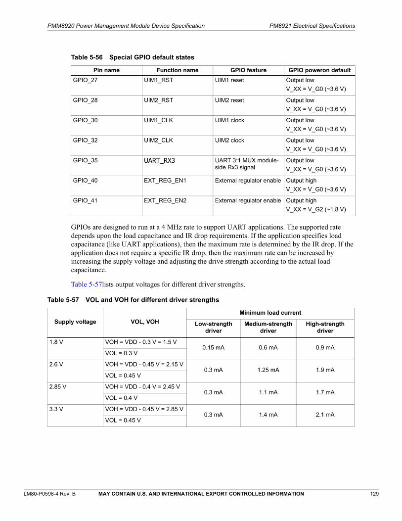
PMM8920 Power Management Module Device Specification PM8921 Electrical Specifications
LM80-P0598-4 Rev. B MAY CONTAIN U.S. AND INTERNATIONAL EXPORT CONTROLLED INFORMATION 129
GPIOs are designed to run at a 4 MHz rate to support UART applications. The supported rate depends upon the load capacitance and IR drop requirements. If the application specifies load capacitance (like UART applications), then the maximum rate is determined by the IR drop. If the application does not require a specific IR drop, then the maximum rate can be increased by increasing the supply voltage and adjusting the drive strength according to the actual load capacitance.
Table 5-57lists output voltages for different driver strengths.
Table 5-56 Special GPIO default states
Pin name Function name GPIO feature GPIO poweron default
GPIO_27 UIM1_RST UIM1 reset Output low
V_XX = V_G0 (~3.6 V)
GPIO_28 UIM2_RST UIM2 reset Output low
V_XX = V_G0 (~3.6 V)
GPIO_30 UIM1_CLK UIM1 clock Output low
V_XX = V_G0 (~3.6 V)
GPIO_32 UIM2_CLK UIM2 clock Output low
V_XX = V_G0 (~3.6 V)
GPIO_35 UART_RX3 UART 3:1 MUX module-side Rx3 signal
Output low
V_XX = V_G0 (~3.6 V)
GPIO_40 EXT_REG_EN1 External regulator enable Output high
V_XX = V_G0 (~3.6 V)
GPIO_41 EXT_REG_EN2 External regulator enable Output high
V_XX = V_G2 (~1.8 V)
Table 5-57 VOL and VOH for different driver strengths
Supply voltage VOL, VOH
Minimum load current
Low-strength driver
Medium-strength driver
High-strength driver
1.8 V VOH = VDD - 0.3 V = 1.5 V0.15 mA 0.6 mA 0.9 mA
VOL = 0.3 V
2.6 V VOH = VDD - 0.45 V = 2.15 V0.3 mA 1.25 mA 1.9 mA
VOL = 0.45 V
2.85 V VOH = VDD - 0.4 V = 2.45 V0.3 mA 1.1 mA 1.7 mA
VOL = 0.4 V
3.3 V VOH = VDD - 0.45 V = 2.85 V0.3 mA 1.4 mA 2.1 mA
VOL = 0.45 V

PMM8920 Power Management Module Device Specification PM8921 Electrical Specifications
LM80-P0598-4 Rev. B MAY CONTAIN U.S. AND INTERNATIONAL EXPORT CONTROLLED INFORMATION 130
5.11 Multipurpose pin specifications
The PMM8160 IC includes 12 multipurpose pins (MPPs), but they can be configured for any of the functions specified within Table 5-58.
All MPPs are high-Z (set as disabled current sinks) except MPP_02 and MPP_04, which are pulled low by default for use with UIM1 and UIM2. MPP_05 supplies 1.25 V from REF_BYP for the reference voltage.
Table 5-58 Multipurpose pin performance specifications
Parameter Comments Min Typ Max Units
MPP configured as digital input11
Logic high input voltage 0.65·VYY1 – – V
Logic low input voltage – – 0.35·VYY1 V
MPP configured as digital output22
Logic high output voltage Iout = IOH VYY2 - 0.45 – VYY2 V
Logic low output voltage Iout = IOL 0 – 0.45 V
MPP configured as bidirectional I/O33
Nominal pull-up resistance Programmable range44 1 – 30 k
Maximum frequency 200 – – kHz
Switch on resistance – 20 50
Power supply current – 6 7 µA
MPP configured as analog input (analog multiplexer input)
Input current – – 100 nA
Input capacitance – – 10 pF
MPP configured as analog output (buffered VREF output)
Output voltage error -50 µA to +50 µA – – 12.5 mV
Temperature variation Due to buffer only; does not include VREF variation (see Table 5-22)
-0.03 – +0.03 %
Load capacitance – – 25 pF
Power supply current – 0.17 0.20 mA
MPP configured as level translator
Maximum frequency 4 – – MHz
1. VYY1 is the programmable supply voltage from which digital input thresholds are referenced; options are listed in Table 2-1. Other specifications are included in Table 5-4.
2. VYY2 is the programmable supply voltage from which digital output thresholds are referenced; options are listed in Table 2-1. Other specifications are included in Table 5-4. The input and output supply voltages can be different.
3. MPP pairs are listed in Table 5-51.4. Pull-up resistance is programmable to values of 1 k, 10 k, 30 k, or open.
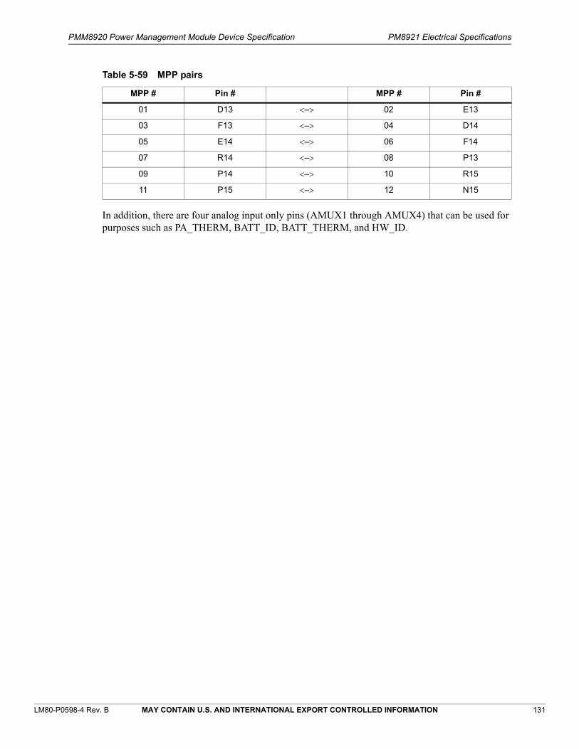
PMM8920 Power Management Module Device Specification PM8921 Electrical Specifications
LM80-P0598-4 Rev. B MAY CONTAIN U.S. AND INTERNATIONAL EXPORT CONTROLLED INFORMATION 131
In addition, there are four analog input only pins (AMUX1 through AMUX4) that can be used for purposes such as PA_THERM, BATT_ID, BATT_THERM, and HW_ID.
Table 5-59 MPP pairs
MPP # Pin # MPP # Pin #
01 D13 – 02 E13
03 F13 – 04 D14
05 E14 – 06 F14
07 R14 – 08 P13
09 P14 – 10 R15
11 P15 – 12 N15
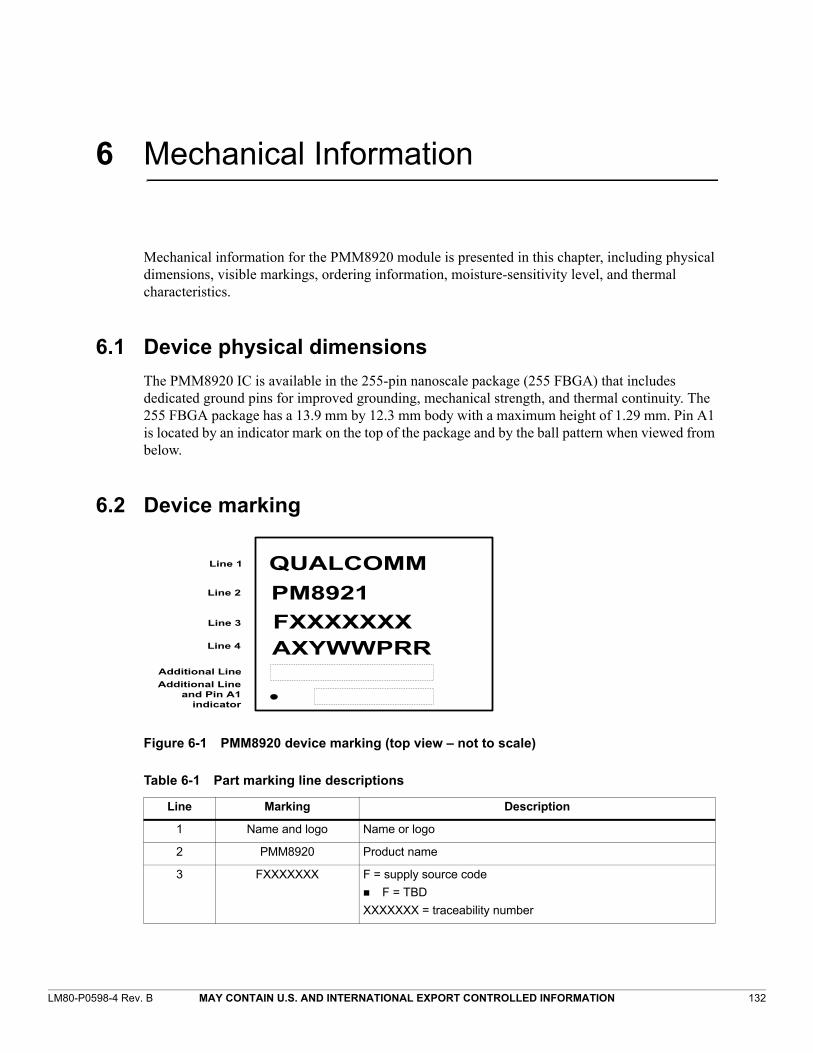
LM80-P0598-4 Rev. B MAY CONTAIN U.S. AND INTERNATIONAL EXPORT CONTROLLED INFORMATION 132
6 Mechanical Information
Mechanical information for the PMM8920 module is presented in this chapter, including physical dimensions, visible markings, ordering information, moisture-sensitivity level, and thermal characteristics.
6.1 Device physical dimensions
The PMM8920 IC is available in the 255-pin nanoscale package (255 FBGA) that includes dedicated ground pins for improved grounding, mechanical strength, and thermal continuity. The 255 FBGA package has a 13.9 mm by 12.3 mm body with a maximum height of 1.29 mm. Pin A1 is located by an indicator mark on the top of the package and by the ball pattern when viewed from below.
6.2 Device marking
Figure 6-1 PMM8920 device marking (top view – not to scale)
Table 6-1 Part marking line descriptions
Line Marking Description
1 Name and logo Name or logo
2 PMM8920 Product name
3 FXXXXXXX F = supply source code
F = TBD
XXXXXXX = traceability number
QUALCOMMPM8921FXXXXXXXAXYWWPRR
Line 1
Line 2
Line 3
Line 4
Additional LineAdditional Line
and Pin A1indicator

PMM8920 Power Management Module Device Specification Mechanical Information
LM80-P0598-4 Rev. B MAY CONTAIN U.S. AND INTERNATIONAL EXPORT CONTROLLED INFORMATION 133
4 AXYWWPRR A = assembly site code
A = TBD
X = traceability number
Y = single-digit year code
WW = work week (based on calendar year)
P = product configuration code (see Table 6-2)
RR = product revision (see Table 6-2)
Additional lines may appear on the part marking for some samples; this is manufacturing information that is only relevant to suppliers.
Table 6-1 Part marking line descriptions
Line Marking Description

PMM8920 Power Management Module Device Specification Mechanical Information
LM80-P0598-4 Rev. B MAY CONTAIN U.S. AND INTERNATIONAL EXPORT CONTROLLED INFORMATION 134
6.3 Device ordering information
This device can be ordered using the identification code shown in Figure 6-2 and explained below.
Figure 6-2 Device identification code
An example can be as follows: PMM8920-0-255FBGA-TR-02-0.
Device ordering information details for all samples available to date are summarized in Table 6-2.
Table 6-2 Device identification code/ordering information details
PMM8920 variant
Product configuration
code (P)
Product revision
(RR)
Sample type
PM8921/PM8821 combination
PMM8920 0 00 ES1 PM8921 ES2 (v2.0) + PM8821 ES1 (v1.0)
PMM8920 0 01 ES2 PM8921 CS (v3.0) + PM8821 ES1 (v1.0)
PMM8920 0 02 ES3 PM8921 CS (v3.0) + PM8821 ES2 (v2.0)
PMM8920 0 04 ES4 PM8921 CS (v3.0) + PM8821 CS (v2.1)
AA-AAAA
RR: Product revision(ex: “02” = engineering sample)
AAA-AAAA: Product name(ex: PM-8821)
P: Configuration code (ex: 0)
BBB: Number of pins (ex: 042)
DD: Packing information(ex: "TR"= tape and reel)
- P - BBB CCC - DD - RR - S
S: Source code (ex: 0)
CCC: Package type (ex: WLNSP)
PMM8920 Power Management Module Device Specification Mechanical Information
LM80-P0598-4 Rev. B MAY CONTAIN U.S. AND INTERNATIONAL EXPORT CONTROLLED INFORMATION 135
6.4 Device moisture-sensitivity level
Plastic-encapsulated surface mount packages are susceptible to damage induced by absorbed moisture and high temperature. The latest IPC/JEDEC J-STD-020 standard revision is followed for moisture-sensitivity qualification. The PMM8920 devices are classified as MSL3 at TBDºC. This is the MSL classification temperature, which is defined as the minimum temperature of moisture sensitivity testing during device qualification.
Additional MSL information is included in:
Section 7.2 – Storage
Section 7.3 – Handling
Section 9.1 – Reliability qualifications summary
6.5 Thermal characteristics
The PMM8160 device in its 255 FBGA package has typical thermal resistances as listed in Table 6-3.
Table 6-3 Device thermal resistance
Parameter Comments Typ Units
JA Thermal resistance, J-to-A Junction-to-ambient (still air)1
1. Junction-to-ambient thermal resistance (JA) is calculated based upon the maximum die junction temperature and the total package power dissipation; ambient temperature is 85°C.
TBD °C/W
JC Thermal resistance, J-to-C Junction-to-case2
2. Junction-to-case thermal resistance (JC) applies to situations in which nearly all the heat flows out the top of the package.
TBD °C/W
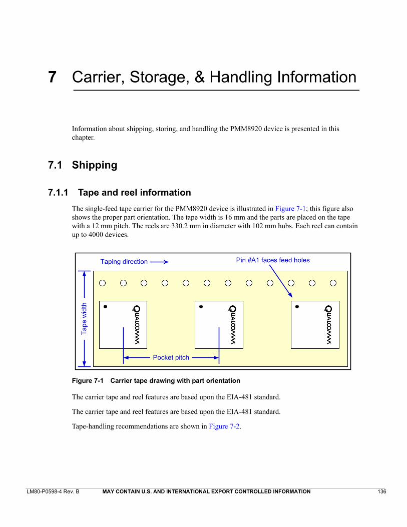
LM80-P0598-4 Rev. B MAY CONTAIN U.S. AND INTERNATIONAL EXPORT CONTROLLED INFORMATION 136
7 Carrier, Storage, & Handling Information
Information about shipping, storing, and handling the PMM8920 device is presented in this chapter.
7.1 Shipping
7.1.1 Tape and reel information
The single-feed tape carrier for the PMM8920 device is illustrated in Figure 7-1; this figure also shows the proper part orientation. The tape width is 16 mm and the parts are placed on the tape with a 12 mm pitch. The reels are 330.2 mm in diameter with 102 mm hubs. Each reel can contain up to 4000 devices.
Figure 7-1 Carrier tape drawing with part orientation
The carrier tape and reel features are based upon the EIA-481 standard.
The carrier tape and reel features are based upon the EIA-481 standard.
Tape-handling recommendations are shown in Figure 7-2.
Pin #A1 faces feed holesTaping direction
Tape
wid
th
Pocket pitch
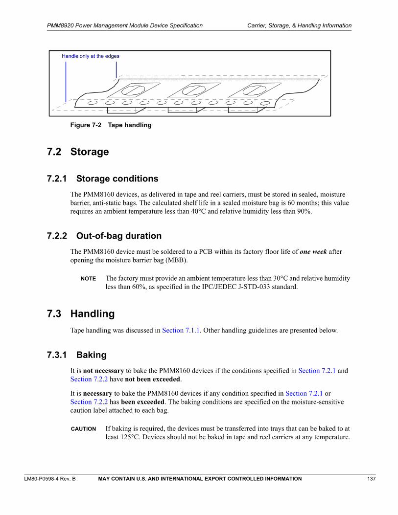
PMM8920 Power Management Module Device Specification Carrier, Storage, & Handling Information
LM80-P0598-4 Rev. B MAY CONTAIN U.S. AND INTERNATIONAL EXPORT CONTROLLED INFORMATION 137
Figure 7-2 Tape handling
7.2 Storage
7.2.1 Storage conditions
The PMM8160 devices, as delivered in tape and reel carriers, must be stored in sealed, moisture barrier, anti-static bags. The calculated shelf life in a sealed moisture bag is 60 months; this value requires an ambient temperature less than 40°C and relative humidity less than 90%.
7.2.2 Out-of-bag duration
The PMM8160 device must be soldered to a PCB within its factory floor life of one week after opening the moisture barrier bag (MBB).
NOTE The factory must provide an ambient temperature less than 30°C and relative humidity less than 60%, as specified in the IPC/JEDEC J-STD-033 standard.
7.3 Handling
Tape handling was discussed in Section 7.1.1. Other handling guidelines are presented below.
7.3.1 Baking
It is not necessary to bake the PMM8160 devices if the conditions specified in Section 7.2.1 and Section 7.2.2 have not been exceeded.
It is necessary to bake the PMM8160 devices if any condition specified in Section 7.2.1 or Section 7.2.2 has been exceeded. The baking conditions are specified on the moisture-sensitive caution label attached to each bag.
CAUTION If baking is required, the devices must be transferred into trays that can be baked to at least 125°C. Devices should not be baked in tape and reel carriers at any temperature.
Handle only at the edges

PMM8920 Power Management Module Device Specification Carrier, Storage, & Handling Information
LM80-P0598-4 Rev. B MAY CONTAIN U.S. AND INTERNATIONAL EXPORT CONTROLLED INFORMATION 138
7.3.2 Electrostatic discharge
Electrostatic discharge (ESD) occurs naturally in laboratory and factory environments. An established high-voltage potential is always at risk of discharging to a lower potential. If this discharge path is through a semiconductor device, destructive damage may result.
ESD countermeasures and handling methods must be developed and used to control the factory environment at each manufacturing site.
These products must be handled according to the ESD Association standard: ANSI/ESD S20.20-1999, Protection of Electrical and Electronic Parts, Assemblies, and Equipment.
Refer to Chapter 7 for the PMM8920 device ESD ratings.
LM80-P0598-4 Rev. B MAY CONTAIN U.S. AND INTERNATIONAL EXPORT CONTROLLED INFORMATION 139
8 PCB Mounting Guidelines
Guidelines for mounting the PMM8920 device onto a printed circuit board (PCB) are presented in this chapter, including land pad and stencil design details, surface mount technology (SMT) process characterization, and SMT process verification.
The PMM8920 device is internally and externally lead-free and RoHS-compliant. Its SnAgCu solder balls use SAC125Ni composition.
NOTE Lead-free (or Pb-free) semiconductor products are defined as having a maximum lead concentration of 1000 ppm (0.1% by weight) in raw (homogeneous) materials and end products.
8.1 Land pattern, stencil design, and daisy-chain interconnect drawings
The land pattern and stencil recommendations presented in this section are based upon characterizations for SnPb and lead-free solder pastes on a four-layer test PCB and a 127 micron-thick stencil. The PCB land pattern and stencil design for the 255 FBGA are the same whether SnPb or lead-free solder is used.
8.2 SSMT development and characterization
The information presented in this section describes board-level characterization process parameters. It is included to assist customers when starting their SMT process development; it is not intended to be a specification for customer SMT processes.
NOTE It is recommended that customers follow their solder paste vendor recommendations for the screen-printing process parameters and reflow profile conditions.
Characterization tests attempt to optimize the SMT process for the best board-level reliability possible. This is done by performing physical tests on evaluation boards, which may include:
Peel test
Bend-to-failure
Bend cycle
Tensile pull

PMM8920 Power Management Module Device Specification PCB Mounting Guidelines
LM80-P0598-4 Rev. B MAY CONTAIN U.S. AND INTERNATIONAL EXPORT CONTROLLED INFORMATION 140
Drop shock
Temperature cycling
It is recommended to characterize the land patterns according to each customer's processes, materials, equipment, stencil design, and reflow profile prior to PCB production. Review the land pattern and stencil pattern design recommendations in Section 8.1 as a guide for characterization.
Optimizing the solder stencil pattern design and print process is critical to ensure print uniformity, decrease voiding, and increase board-level reliability.
Reflow profile conditions typically used for SnPb and lead-free systems are given in Table 8-1.
8.3 SMT peak package body temperature
The following limits are recommended during the SMT board-level solder attach process:
SMT peak package body temperature of 250°C – the temperature that should not be exceeded as measured on the package body’s top surface
Maximum duration of 40 sec at this temperature
Although the solder paste manufacturers’ recommendations for optimum temperature and duration for solder reflow should be followed, the recommended limits must not be exceeded.
8.4 SMT process verification
It is recommended to verify the SMT process prior to high-volume PCB fabrication, including:
Electrical continuity
X-ray inspection of the package installation for proper alignment, solder voids, solder balls, and solder bridging
Visual inspection
Cross-section inspection of solder joints to confirm registration, fillet shape, and print volume (insufficient, acceptable, or excessive)
Table 8-1 Typical SMT reflow profile conditions (for reference only)
Profile stage DescriptionSnPb (standard) condition limits
Lead-free (high-temp) condition limits
Preheat Initial ramp 3°C/sec max 3°C/sec max
Soak Dry out and flux activation 135 to 165°C
60 to 120 sec
135 to 175°C
60 to 120 sec
Reflow Time above solder paste melting point 30 to 90 sec 40 to 90 sec
SMT peak package body temperature 230°C 245°C
Cool down Cool rate – ramp-to-ambient 6°C/sec max 6°C/sec max

LM80-P0598-4 Rev. B MAY CONTAIN U.S. AND INTERNATIONAL EXPORT CONTROLLED INFORMATION 141
9 Part Reliability
9.1 Reliability qualifications summary
Table 9-1 PMM8160 IC reliability evaluation
Tests, standards, and conditions Sample size Results
Average failure rate (AFR) in FIT () failure in billion device-hours
HTOL: JESD22-A108-C
TBD TBD
Mean time to failure (MTTF) t = 1/ in million hours
TBD TBD
ESD – human-body model (HBM) rating
JESD22-A114-E
TBD TBD
ESD – charge-device model (CDM) rating
JESD22-C101-C
TBD TBD
Latch-up: EIA/JESD78A
Temperature = 85°C
TBD TBD
Moisture resistance test (MRT): J-STD-020-C
Reflow at 260 +0/-5°C, MSL = 3
TBD TBD
Temperature cycle: JESD22-A104-C, Cond. B, 1000 cycles
Preconditioning: JESD22-A113-E
TBD TBD
Un-biased highly accelerated stress test (HAST)
JESD22-A118; time = 96 hrs
Preconditioning: JESD22-A113-E
TBD TBD
High-temperature storage life: JESD22-A103-C
Temperature = 150°C; time = 1000 hrs
TBD TBD
Flammability
UL-STD-94 (by mold-compound certification)
TBD TBD
Physical dimensions
JESD22-B100-B
TBD TBD
Solder ball shear
JESD22-B117A
TBD TBD
PMM8920 Power Management Module Device Specification Part Reliability
LM80-P0598-4 Rev. B MAY CONTAIN U.S. AND INTERNATIONAL EXPORT CONTROLLED INFORMATION 142
9.2 Qualification sample description
Device characteristics:
Device name: PMM8920
Package type: 255 FBGA
Package body size: 13.9 mm × 12.3 mm × 1.29 mm
Pad count: 255
Pad composition: Sn/Ag/Cu
Processes: 0.18 CMOS
Fab sites: TBD
Assembly sites: TBD
Solder ball pitch: 0.8 mm
LM80-P0598-4 Rev. B MAY CONTAIN U.S. AND INTERNATIONAL EXPORT CONTROLLED INFORMATION 143
10 Exhibit 1
PLEASE READ THIS LICENSE AGREEMENT (“AGREEMENT”) CAREFULLY. THIS AGREEMENT IS A BINDING LEGAL AGREEMENT ENTERED INTO BY AND BETWEEN YOU (OR IF YOU ARE ENTERING INTO THIS AGREEMENT ON BEHALF OF AN ENTITY, THEN THE ENTITY THAT YOU REPRESENT) AND QUALCOMM TECHNOLOGIES, INC. (“QTI” “WE” “OUR” OR “US”). THIS IS THE AGREEMENT THAT APPLIES TO YOUR USE OF THE DESIGNATED AND/OR ATTACHED DOCUMENTATION AND ANY UPDATES OR IMPROVEMENTS THEREOF (COLLECTIVELY, “MATERIALS”). BY USING OR COMPLETING THE INSTALLATION OF THE MATERIALS, YOU ARE ACCEPTING THIS AGREEMENT AND YOU AGREE TO BE BOUND BY ITS TERMS AND CONDITIONS. IF YOU DO NOT AGREE TO THESE TERMS, QTI IS UNWILLING TO AND DOES NOT LICENSE THE MATERIALS TO YOU. IF YOU DO NOT AGREE TO THESE TERMS YOU MUST DISCONTINUE AND YOU MAY NOT USE THE MATERIALS OR RETAIN ANY COPIES OF THE MATERIALS. ANY USE OR POSSESSION OF THE MATERIALS BY YOU IS SUBJECT TO THE TERMS AND CONDITIONS SET FORTH IN THIS AGREEMENT.
1.1 License. Subject to the terms and conditions of this Agreement, including, without limitation, the restrictions, conditions, limitations and exclusions set forth in this Agreement, Qualcomm Technologies, Inc. (“QTI”) hereby grants to you a nonexclusive, limited license under QTI’s copyrights to use the attached Materials; and to reproduce and redistribute a reasonable number of copies of the Materials. You may not use Qualcomm Technologies or its affiliates or subsidiaries name, logo or trademarks; and copyright, trademark, patent and any other notices that appear on the Materials may not be removed or obscured. QTI shall be free to use suggestions, feedback or other information received from You, without obligation of any kind to You. QTI may immediately terminate this Agreement upon your breach. Upon termination of this Agreement, Sections 1.2-4 shall survive.
1.2 Indemnification. You agree to indemnify and hold harmless QTI and its officers, directors, employees and successors and assigns against any and all third party claims, demands, causes of action, losses, liabilities, damages, costs and expenses, incurred by QTI (including but not limited to costs of defense, investigation and reasonable attorney’s fees) arising out of, resulting from or related to: (i) any breach of this Agreement by You; and (ii) your acts, omissions, products and services. If requested by QTI, You agree to defend QTI in connection with any third party claims, demands, or causes of action resulting from, arising out of or in connection with any of the foregoing.
1.3 Ownership. QTI (or its licensors) shall retain title and all ownership rights in and to the Materials and all copies thereof, and nothing herein shall be deemed to grant any right to You under any of QTI's or its affiliates’ patents. You shall not subject the Materials to any third party license terms (e.g., open source license terms). You shall not use the Materials for the purpose of identifying or providing evidence to support any potential patent infringement claim against QTI, its affiliates, or any of QTI’s or QTI’s affiliates’ suppliers and/or direct or indirect customers. QTI hereby reserves all rights not expressly granted herein.
1.4 WARRANTY DISCLAIMER. YOU EXPRESSLY ACKNOWLEDGE AND AGREE THAT THE USE OF THE MATERIALS IS AT YOUR SOLE RISK. THE MATERIALS AND TECHNICAL SUPPORT, IF ANY, ARE PROVIDED "AS IS" AND WITHOUT WARRANTY OF ANY KIND, WHETHER EXPRESS OR IMPLIED. QTI ITS LICENSORS AND AFFILIATES MAKE NO WARRANTIES, EXPRESS OR IMPLIED, WITH RESPECT TO THE MATERIALS OR ANY OTHER INFORMATION OR DOCUMENTATION PROVIDED UNDER THIS AGREEMENT, INCLUDING BUT NOT LIMITED TO ANY WARRANTY OF MERCHANTABILITY OR FITNESS FOR A PARTICULAR PURPOSE OR AGAINST INFRINGEMENT, OR ANY EXPRESS OR IMPLIED WARRANTY ARISING OUT OF TRADE USAGE OR OUT OF A COURSE OF DEALING OR COURSE OF PERFORMANCE. NOTHING CONTAINED IN THIS AGREEMENT SHALL BE CONSTRUED AS (I) A WARRANTY OR REPRESENTATION BY QTI, ITS LICENSORS OR AFFILIATES AS TO THE VALIDITY OR SCOPE OF ANY PATENT, COPYRIGHT OR OTHER INTELLECTUAL PROPERTY RIGHT OR (II) A WARRANTY OR REPRESENTATION BY QTI THAT ANY MANUFACTURE OR USE WILL BE FREE FROM INFRINGEMENT OF PATENTS, COPYRIGHTS OR OTHER INTELLECTUAL PROPERTY RIGHTS OF OTHERS, AND IT SHALL BE THE SOLE RESPONSIBILITY OF YOU TO MAKE SUCH DETERMINATION AS IS NECESSARY WITH RESPECT TO THE ACQUISITION OF LICENSES UNDER PATENTS AND OTHER INTELLECTUAL PROPERTY OF THIRD PARTIES.
1.5 LIMITATION OF LIABILITY. IN NO EVENT SHALL QTI, QTI’S AFFILIATES OR ITS LICENSORS BE LIABLE TO YOU FOR ANY INCIDENTAL, CONSEQUENTIAL OR SPECIAL DAMAGES, INCLUDING BUT NOT LIMITED TO ANY LOST PROFITS, LOST SAVINGS, OR OTHER INCIDENTAL DAMAGES, ARISING OUT OF THE USE OR INABILITY TO USE, OR THE DELIVERY OR FAILURE TO DELIVER, ANY OF THE MATERIALS, OR ANY BREACH OF ANY OBLIGATION UNDER THIS AGREEMENT, EVEN IF QTI HAS BEEN ADVISED OF THE POSSIBILITY OF SUCH DAMAGES. THE FOREGOING LIMITATION OF LIABILITY SHALL REMAIN IN FULL FORCE AND EFFECT

PMM8920 Power Management Module Device Specification Exhibit 1
LM80-P0598-4 Rev. B MAY CONTAIN U.S. AND INTERNATIONAL EXPORT CONTROLLED INFORMATION 144
REGARDLESS OF WHETHER YOUR REMEDIES HEREUNDER ARE DETERMINED TO HAVE FAILED OF THEIR ESSENTIAL PURPOSE. THE ENTIRE LIABILITY OF QTI, QTI’s AFFILIATES AND ITS LICENSORS, AND THE SOLE AND EXCLUSIVE REMEDY OF YOU, FOR ANY CLAIM OR CAUSE OF ACTION ARISING HEREUNDER (WHETHER IN CONTRACT, TORT, OR OTHERWISE) SHALL NOT EXCEED US$10.
2. COMPLIANCE WITH LAWS; APPLICABLE LAW. You agree to comply with all applicable local, international and national laws and regulations and with U.S. Export Administration Regulations, as they apply to the subject matter of this Agreement. This Agreement is governed by the laws of the State of California, excluding California’s choice of law rules.
3. CONTRACTING PARTIES. If the Materials are downloaded on any computer owned by a corporation or other legal entity, then this Agreement is formed by and between QTI and such entity. The individual accepting the terms of this Agreement represents and warrants to QTI that they have the authority to bind such entity to the terms and conditions of this Agreement.
4. MISCELLANEOUS PROVISIONS. This Agreement, together with all exhibits attached hereto, which are incorporated herein by
this reference, constitutes the entire agreement between QTI and You and supersedes all prior negotiations, representations and
agreements between the parties with respect to the subject matter hereof. No addition or modification of this Agreement shall be
effective unless made in writing and signed by the respective representatives of QTI and You. The restrictions, limitations, exclusions
and conditions set forth in this Agreement shall apply even if QTI or any of its affiliates becomes aware of or fails to act in a manner to
address any violation or failure to comply therewith. You hereby acknowledge and agree that the restrictions, limitations, conditions
and exclusions imposed in this Agreement on the rights granted in this Agreement are not a derogation of the benefits of such rights.
You further acknowledges that, in the absence of such restrictions, limitations, conditions and exclusions, QTI would not have entered
into this Agreement with You. Each party shall be responsible for and shall bear its own expenses in connection with this Agreement. If
any of the provisions of this Agreement are determined to be invalid, illegal, or otherwise unenforceable, the remaining provisions shall
remain in full force and effect. This Agreement is entered into solely in the English language, and if for any reason any other language
version is prepared by any party, it shall be solely for convenience and the English version shall govern and control all aspects. If You
are located in the province of Quebec, Canada, the following applies: The Parties hereby confirm they have requested this Agreement
and all related documents be prepared in English.