pin 1 mark single phase low noise smart … phase low noise smart motor driver 6 description the...
TRANSCRIPT
AH9485/86 Document number: DS38108 Rev. 1 - 2
1 of 12 www.diodes.com
September 2015 © Diodes Incorporated
AH9485/86
NE
W P
RO
DU
CT
SINGLE PHASE LOW NOISE SMART MOTOR DRIVER
Description The AH9485 and AH9486 are single chip solutions for driving a single phase (coil) brushless DC motors. It integrates the motor driver and the high sensitivity Hall effect sensor to simplify the system circuit and PCB design for simpler solutions. Rotor lock-detect, shutdown and auto-restart functions help to prevent the motor from over-heating when rotor is locked and restarts the motor after the lock is removed. The AH9485 and AH9486 have built-in open drain tachometer frequency generator (FG) and rotation detection (RD) outputs to allow external interface to monitor motor rotation, speed or rotor locks conditions easily. The FG provides magnetic change frequency while the RD provides the rotor status. The full bridge output stage uses “soft-switching” technique to minimize the audible switching noise (vibration and acoustic noise) and electromagnetic interference (EMI) providing a low noise solution. Over-temperature shutdown provides thermal protection for the device. An external DC voltage or a PWM (pulse-width modulation) signal on the PWM pin can be used to control the motor speed. The AH9485 and AH9486 are packaged in TSOT26F.
Features
Internal Full Bridge Driver
High Sensitivity Integrated Hall Sensor
Low and Wide Supply Voltage Range of 2V to 6V
Soft Switching for Low Noise
Rotor Lock Protection and Auto-Restart
DC Voltage or PWM Signal Speed Control
Thermal Protection
Tachometer FG Output(AH9485) or Rotor Lock Alarm RD Output
(AH9486)
Operating Temperature Range of -40ºC to +105ºC
Flat Pin TSOT26F Package
Totally Lead-Free & Fully RoHS Compliant (Notes 1 & 2)
Halogen and Antimony Free. “Green” Device (Note 3)
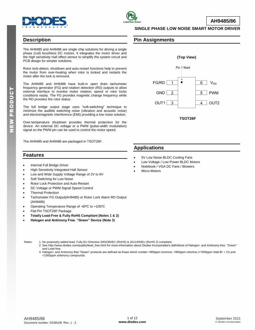
Pin Assignments
(Top View)
1
43
2 5
6
Pin 1 Mark
FG/RD
GND
OUT1 OUT2
PWM
VDD
TSOT26F
Applications
5V Low Noise BLDC Cooling Fans
Low Voltage / Low Power BLDC Motors
Notebook / VGA DC Fans / Blowers
Micro-Motors
Notes: 1. No purposely added lead. Fully EU Directive 2002/95/EC (RoHS) & 2011/65/EU (RoHS 2) compliant. 2. See http://www.diodes.com/quality/lead_free.html for more information about Diodes Incorporated’s definitions of Halogen- and Antimony-free, "Green" and Lead-free. 3. Halogen- and Antimony-free "Green” products are defined as those which contain <900ppm bromine, <900ppm chlorine (<1500ppm total Br + Cl) and <1000ppm antimony compounds.
AH9485/86 Document number: DS38108 Rev. 1 - 2
2 of 12 www.diodes.com
September 2015 © Diodes Incorporated
AH9485/86
NE
W P
RO
DU
CT
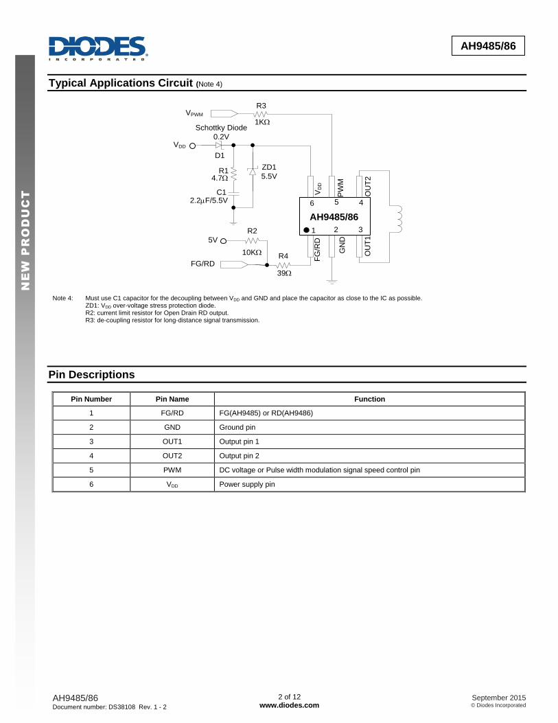
Typical Applications Circuit (Note 4)
6 5 4
OU
T2
1 2 3
OU
T1
GN
D
VD
D
PW
M
10KW
R2
5V
AH9485/86
VPWM
FG
/RD
1KW
R3
4.7W
2.2mF/5.5V
VDD
R1
C1
Schottky Diode
0.2V
ZD1
5.5V
D1
R4
39W
FG/RD
Note 4: Must use C1 capacitor for the decoupling between VDD and GND and place the capacitor as close to the IC as possible.
ZD1: VDD over-voltage stress protection diode. R2: current limit resistor for Open Drain RD output. R3: de-coupling resistor for long-distance signal transmission.
Pin Descriptions
Pin Number Pin Name Function
1 FG/RD FG(AH9485) or RD(AH9486)
2 GND Ground pin
3 OUT1 Output pin 1
4 OUT2 Output pin 2
5 PWM DC voltage or Pulse width modulation signal speed control pin
6 VDD Power supply pin
AH9485/86 Document number: DS38108 Rev. 1 - 2
3 of 12 www.diodes.com
September 2015 © Diodes Incorporated
AH9485/86
NE
W P
RO
DU
CT
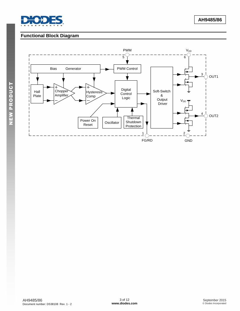
Functional Block Diagram
Hall
Plate
Chopper
AmplifierHysteresis
Comp
Digital
Control
Logic
OscillatorPower On
Reset
Thermal
Shutdown
Protection
Soft-Switch
&
Output
Driver
Bias Generator PWM Control
VDD
PWM VDD
OUT1
OUT2
GNDFG/RD
1 2
3
4
65
AH9485/86 Document number: DS38108 Rev. 1 - 2
4 of 12 www.diodes.com
September 2015 © Diodes Incorporated
AH9485/86
NE
W P
RO
DU
CT
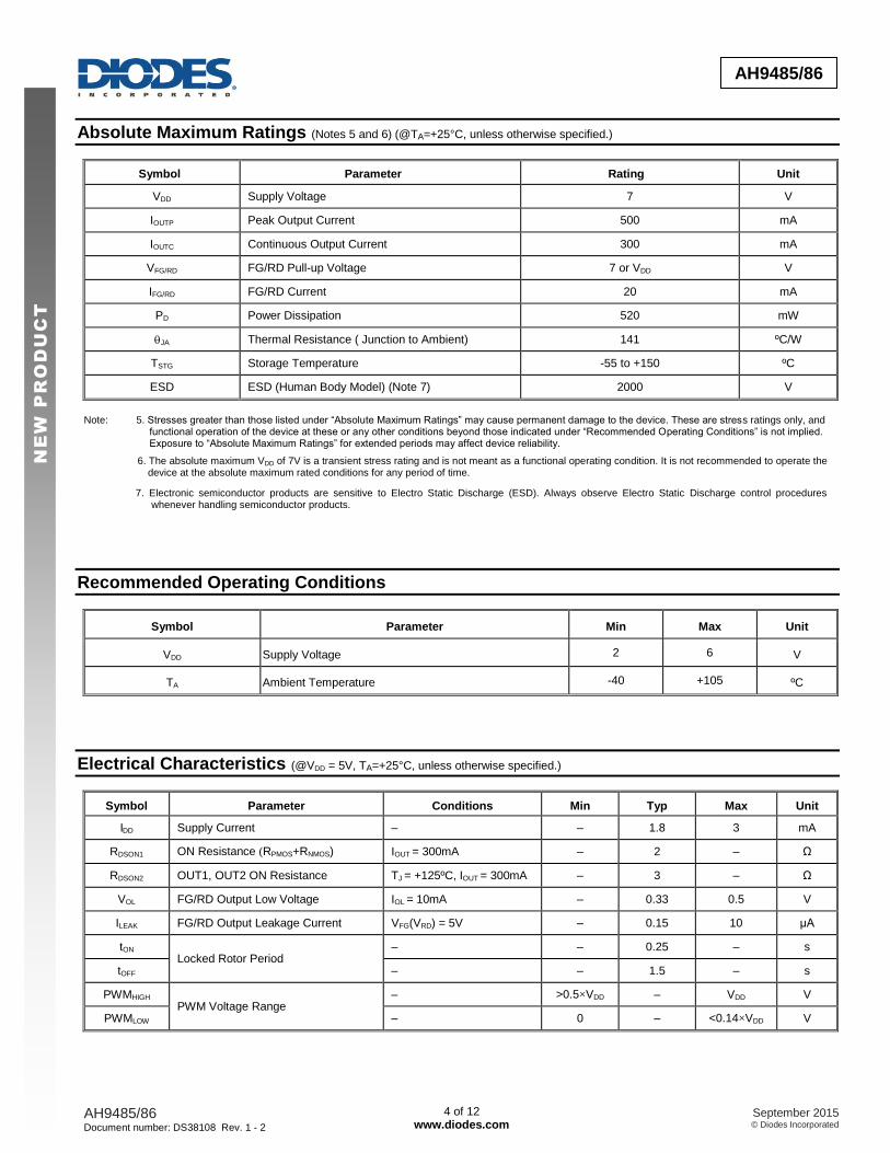
Absolute Maximum Ratings (Notes 5 and 6) (@TA=+25°C, unless otherwise specified.)
Symbol Parameter Rating Unit
VDD Supply Voltage 7 V
IOUTP Peak Output Current 500 mA
IOUTC Continuous Output Current 300 mA
VFG/RD FG/RD Pull-up Voltage 7 or VDD V
IFG/RD FG/RD Current 20 mA
PD Power Dissipation 520 mW
JA Thermal Resistance ( Junction to Ambient) 141 ºC/W
TSTG Storage Temperature -55 to +150 ºC
ESD ESD (Human Body Model) (Note 7) 2000 V
Note: 5. Stresses greater than those listed under “Absolute Maximum Ratings” may cause permanent damage to the device. These are stress ratings only, and
functional operation of the device at these or any other conditions beyond those indicated under “Recommended Operating Conditions” is not implied. Exposure to “Absolute Maximum Ratings” for extended periods may affect device reliability.
6. The absolute maximum VDD of 7V is a transient stress rating and is not meant as a functional operating condition. It is not recommended to operate the device at the absolute maximum rated conditions for any period of time.
7. Electronic semiconductor products are sensitive to Electro Static Discharge (ESD). Always observe Electro Static Discharge control procedures whenever handling semiconductor products.
Recommended Operating Conditions
Symbol Parameter Min Max Unit
VDD Supply Voltage 2 6 V
TA Ambient Temperature -40 +105 ºC
Electrical Characteristics (@VDD = 5V, TA=+25°C, unless otherwise specified.)
Symbol Parameter Conditions Min Typ Max Unit
IDD Supply Current – – 1.8 3 mA
RDSON1 ON Resistance (RPMOS+RNMOS) IOUT = 300mA – 2 – Ω
RDSON2 OUT1, OUT2 ON Resistance TJ = +125ºC, IOUT = 300mA – 3 – Ω
VOL FG/RD Output Low Voltage IOL = 10mA – 0.33 0.5 V
ILEAK FG/RD Output Leakage Current VFG(VRD) = 5V – 0.15 10 μA
tON Locked Rotor Period
– – 0.25 – s
tOFF – – 1.5 – s
PWMHIGH PWM Voltage Range
– >0.5×VDD – VDD V
PWMLOW – 0 – <0.14×VDD V
AH9485/86 Document number: DS38108 Rev. 1 - 2
5 of 12 www.diodes.com
September 2015 © Diodes Incorporated
AH9485/86
NE
W P
RO
DU
CT
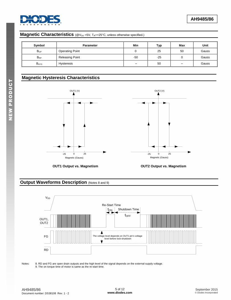
Magnetic Characteristics (@VDD =5V, TA=+25°C, unless otherwise specified.)
Symbol Parameter Min Typ Max Unit
BOP Operating Point 0 25 50 Gauss
BRP Releasing Point -50 -25 0 Gauss
BHYS Hysteresis – 50 – Gauss
Magnetic Hysteresis Characteristics
25-25
Magnetic (Gauss)
OUT1 (V)
0
25-25
Magnetic (Gauss)
OUT2 (V)
0
OUT1 Output vs. Magnetism OUT2 Output vs. Magnetism
Output Waveforms Description (Notes 8 and 9)
tON
Re-Start Time
Shutdown Time
tOFF
VDD
OUT1,
OUT2
FG The voltage level depends on OUT1 pin’s voltage
level before lock-shutdown
RD
Notes: 8. RD and FG are open drain outputs and the high level of the signal depends on the external supply voltage.
9. The on torque time of motor is same as the re-start time.
AH9485/86 Document number: DS38108 Rev. 1 - 2
6 of 12 www.diodes.com
September 2015 © Diodes Incorporated
AH9485/86
NE
W P
RO
DU
CT
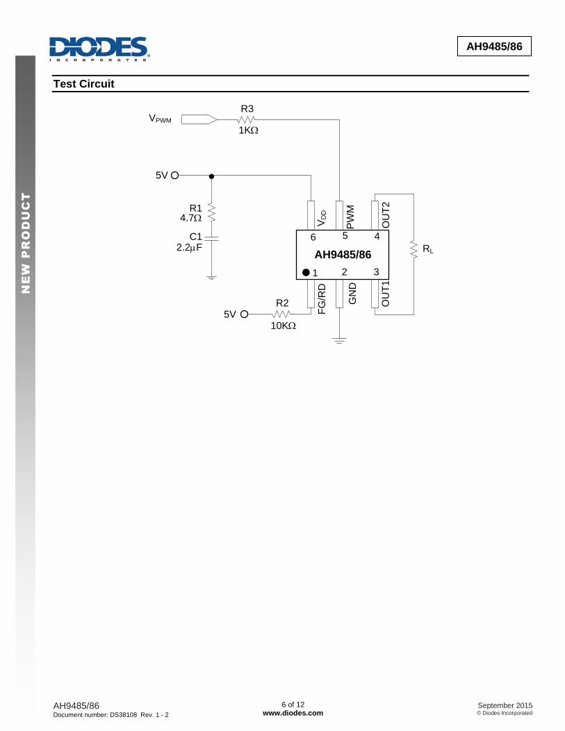
Test Circuit
6 5 4
OU
T2
1 2 3
OU
T1
GN
D
VD
D
PW
M
4.7W
2.2mF
5V
R1
C1
10KW
R25V
AH9485/86
VPWM
RL
FG
/RD
1KW
R3
AH9485/86 Document number: DS38108 Rev. 1 - 2
7 of 12 www.diodes.com
September 2015 © Diodes Incorporated
AH9485/86
NE
W P
RO
DU
CT
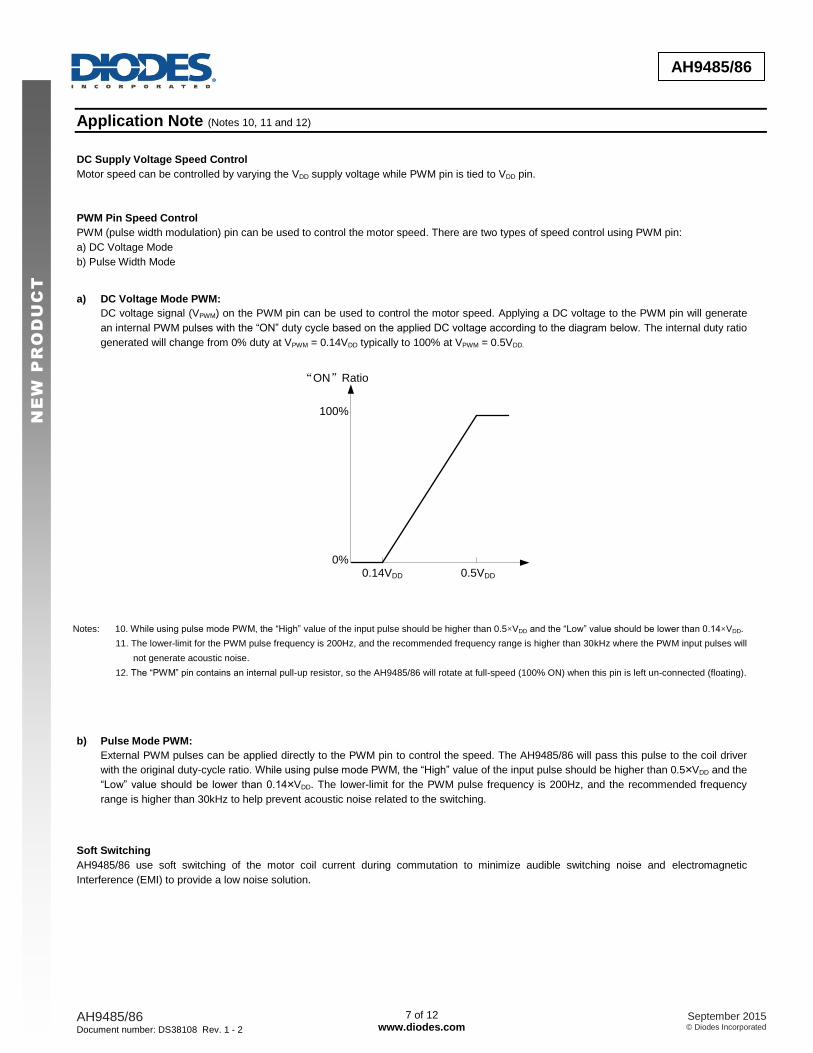
Application Note (Notes 10, 11 and 12)
DC Supply Voltage Speed Control
Motor speed can be controlled by varying the VDD supply voltage while PWM pin is tied to VDD pin.
PWM Pin Speed Control
PWM (pulse width modulation) pin can be used to control the motor speed. There are two types of speed control using PWM pin:
a) DC Voltage Mode
b) Pulse Width Mode
a) DC Voltage Mode PWM:
DC voltage signal (VPWM) on the PWM pin can be used to control the motor speed. Applying a DC voltage to the PWM pin will generate
an internal PWM pulses with the “ON” duty cycle based on the applied DC voltage according to the diagram below. The internal duty ratio
generated will change from 0% duty at VPWM = 0.14VDD typically to 100% at VPWM = 0.5VDD.
0.14VDD 0.5VDD
100%
“ON”Ratio
0%
Notes: 10. While using pulse mode PWM, the “High” value of the input pulse should be higher than 0.5×VDD and the “Low” value should be lower than 0.14×VDD.
11. The lower-limit for the PWM pulse frequency is 200Hz, and the recommended frequency range is higher than 30kHz where the PWM input pulses will
not generate acoustic noise.
12. The “PWM” pin contains an internal pull-up resistor, so the AH9485/86 will rotate at full-speed (100% ON) when this pin is left un-connected (floating).
b) Pulse Mode PWM:
External PWM pulses can be applied directly to the PWM pin to control the speed. The AH9485/86 will pass this pulse to the coil driver
with the original duty-cycle ratio. While using pulse mode PWM, the “High” value of the input pulse should be higher than 0.5×VDD and the
“Low” value should be lower than 0.14×VDD. The lower-limit for the PWM pulse frequency is 200Hz, and the recommended frequency
range is higher than 30kHz to help prevent acoustic noise related to the switching.
Soft Switching
AH9485/86 use soft switching of the motor coil current during commutation to minimize audible switching noise and electromagnetic
Interference (EMI) to provide a low noise solution.
AH9485/86 Document number: DS38108 Rev. 1 - 2
8 of 12 www.diodes.com
September 2015 © Diodes Incorporated
AH9485/86
NE
W P
RO
DU
CT
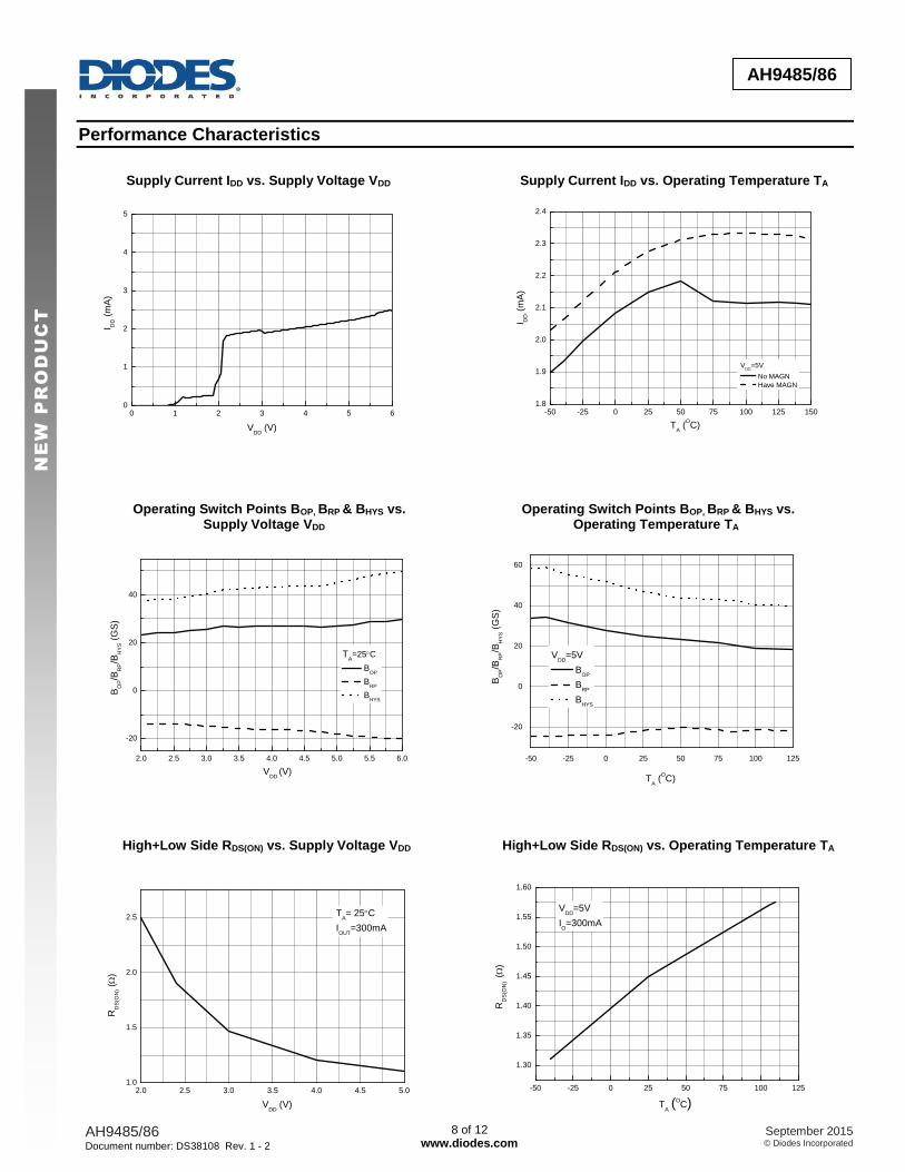
Performance Characteristics
Supply Current IDD vs. Supply Voltage VDD
Supply Current IDD vs. Operating Temperature TA
Operating Switch Points BOP, BRP & BHYS vs. Operating Switch Points BOP, BRP & BHYS vs. Supply Voltage VDD Operating Temperature TA
High+Low Side RDS(ON) vs. Supply Voltage VDD High+Low Side RDS(ON) vs. Operating Temperature TA
0 1 2 3 4 5 60
1
2
3
4
5
I DD (
mA
)
VDD
(V)
2.0 2.5 3.0 3.5 4.0 4.5 5.01.0
1.5
2.0
2.5
RD
S(O
N) (W
)
VDD
(V)
TA= 25C
IOUT
=300mA
2.0 2.5 3.0 3.5 4.0 4.5 5.0 5.5 6.0
-20
0
20
40
BO
P/B
RP/B
HY
S (
GS
)
VDD
(V)
TA=25C
BOP
BRP
BHYS
-50 -25 0 25 50 75 100 125 1501.8
1.9
2.0
2.1
2.2
2.3
2.4
I DD (
mA
)
TA (
OC)
VDD
=5V
No MAGN
Have MAGN
-50 -25 0 25 50 75 100 125
-20
0
20
40
60
BO
P/B
RP/B
HY
S (
GS
)
TA (
OC)
VDD
=5V
BOP
BRP
BHYS
-50 -25 0 25 50 75 100 125
1.30
1.35
1.40
1.45
1.50
1.55
1.60
RD
S(O
N) (
W)
TA (O
C)
VDD
=5V
IO=300mA
AH9485/86 Document number: DS38108 Rev. 1 - 2
9 of 12 www.diodes.com
September 2015 © Diodes Incorporated
AH9485/86
NE
W P
RO
DU
CT
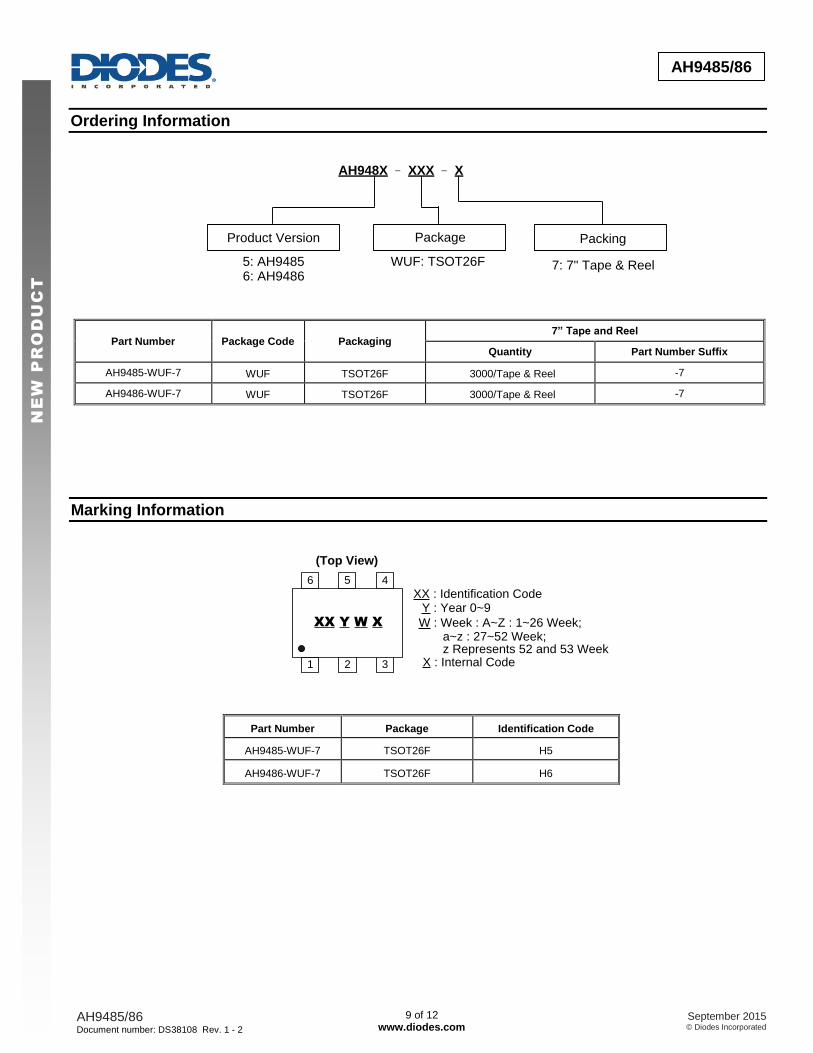
Ordering Information
Package Packing
WUF: TSOT26F
AH948X – XXX – X
Product Version
5: AH94856: AH9486
7: 7" Tape & Reel
Part Number Package Code Packaging 7” Tape and Reel
Quantity Part Number Suffix
AH9485-WUF-7 WUF TSOT26F 3000/Tape & Reel -7
AH9486-WUF-7 WUF TSOT26F 3000/Tape & Reel -7
Marking Information
1 2 3
6 74
XX Y W X
XX : Identification Code
W : Week : A~Z : 1~26 Week;
X : Internal Code
(Top View)
Y : Year 0~9
a~z : 27~52 Week; z Represents 52 and 53 Week
5
Part Number Package Identification Code
AH9485-WUF-7 TSOT26F H5
AH9486-WUF-7 TSOT26F H6
AH9485/86 Document number: DS38108 Rev. 1 - 2
10 of 12 www.diodes.com
September 2015 © Diodes Incorporated
AH9485/86
NE
W P
RO
DU
CT
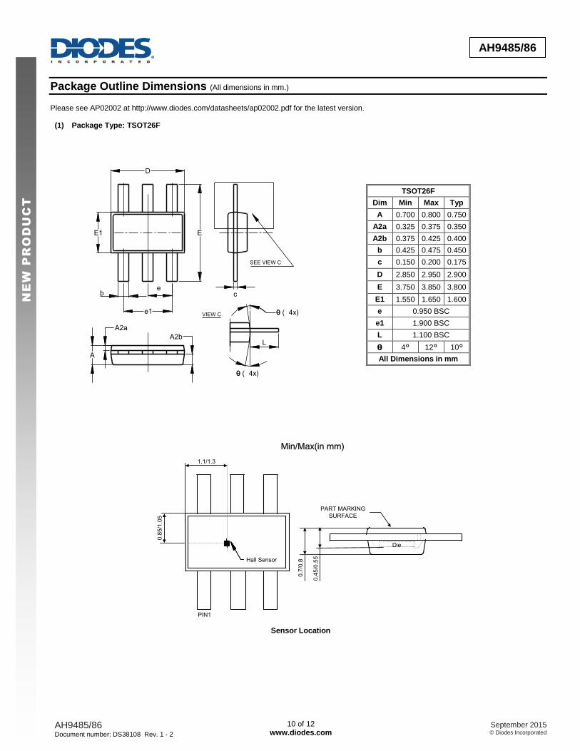
Package Outline Dimensions (All dimensions in mm.)
Please see AP02002 at http://www.diodes.com/datasheets/ap02002.pdf for the latest version. (1) Package Type: TSOT26F
0.8
5/1
.05
1.1/1.3
Hall Sensor
Min/Max(in mm)
0.4
5/0
.55
0.7
/0.8
Die
PART MARKING
SURFACE
PIN1
Sensor Location
SEE VIEW C
A
VIEW C
0 (4x)
0 (4x)e1
E
e
E1
D
b c
A2a
A2bL
TSOT26F
Dim Min Max Typ
A 0.700 0.800 0.750
A2a 0.325 0.375 0.350
A2b 0.375 0.425 0.400
b 0.425 0.475 0.450
c 0.150 0.200 0.175
D 2.850 2.950 2.900
E 3.750 3.850 3.800
E1 1.550 1.650 1.600
e 0.950 BSC
e1 1.900 BSC
L 1.100 BSC
θ 4° 12° 10°
All Dimensions in mm
AH9485/86 Document number: DS38108 Rev. 1 - 2
11 of 12 www.diodes.com
September 2015 © Diodes Incorporated
AH9485/86
NE
W P
RO
DU
CT
Mechanical Structure
Rotor
Magnet
PCB PCB
Rotor Height Vertical Heighth1 h2PCB Thickness
h3
IC Ink View
Soldering Thickness
h4
Suggested Pad Layout Please see AP02001 at http://www.diodes.com/datasheets/ap02001.pdf for the latest version. (1) Package Type: TSOT26F
Y1
C X
Y
X1
Dimensions Value
(in mm)
C 0.950
X 0.700
X1 2.600
Y 1.000
Y1 4.220
AH9485/86 Document number: DS38108 Rev. 1 - 2
12 of 12 www.diodes.com
September 2015 © Diodes Incorporated
AH9485/86
NE
W P
RO
DU
CT
IMPORTANT NOTICE DIODES INCORPORATED MAKES NO WARRANTY OF ANY KIND, EXPRESS OR IMPLIED, WITH REGARDS TO THIS DOCUMENT, INCLUDING, BUT NOT LIMITED TO, THE IMPLIED WARRANTIES OF MERCHANTABILITY AND FITNESS FOR A PARTICULAR PURPOSE (AND THEIR EQUIVALENTS UNDER THE LAWS OF ANY JURISDICTION). Diodes Incorporated and its subsidiaries reserve the right to make modifications, enhancements, improvements, corrections or other changes without further notice to this document and any product described herein. Diodes Incorporated does not assume any liability arising out of the application or use of this document or any product described herein; neither does Diodes Incorporated convey any license under its patent or trademark rights, nor the rights of others. Any Customer or user of this document or products described herein in such applications shall assume all risks of such use and will agree to hold Diodes Incorporated and all the companies whose products are represented on Diodes Incorporated website, harmless against all damages. Diodes Incorporated does not warrant or accept any liability whatsoever in respect of any products purchased through unauthorized sales channel. Should Customers purchase or use Diodes Incorporated products for any unintended or unauthorized application, Customers shall indemnify and hold Diodes Incorporated and its representatives harmless against all claims, damages, expenses, and attorney fees arising out of, directly or indirectly, any claim of personal injury or death associated with such unintended or unauthorized application. Products described herein may be covered by one or more United States, international or foreign patents pending. Product names and markings noted herein may also be covered by one or more United States, international or foreign trademarks. This document is written in English but may be translated into multiple languages for reference. Only the English version of this document is the final and determinative format released by Diodes Incorporated.
LIFE SUPPORT Diodes Incorporated products are specifically not authorized for use as critical components in life support devices or systems without the express written approval of the Chief Executive Officer of Diodes Incorporated. As used herein: A. Life support devices or systems are devices or systems which: 1. are intended to implant into the body, or
2. support or sustain life and whose failure to perform when properly used in accordance with instructions for use provided in the labeling can be reasonably expected to result in significant injury to the user.
B. A critical component is any component in a life support device or system whose failure to perform can be reasonably expected to cause the failure of the life support device or to affect its safety or effectiveness. Customers represent that they have all necessary expertise in the safety and regulatory ramifications of their life support devices or systems, and acknowledge and agree that they are solely responsible for all legal, regulatory and safety-related requirements concerning their products and any use of Diodes Incorporated products in such safety-critical, life support devices or systems, notwithstanding any devices- or systems-related information or support that may be provided by Diodes Incorporated. Further, Customers must fully indemnify Diodes Incorporated and its representatives against any damages arising out of the use of Diodes Incorporated products in such safety-critical, life support devices or systems. Copyright © 2015, Diodes Incorporated www.diodes.com