piezoresistance in silicon dr. lynn fuller - rit - … · piezoresistance in silicon dr. lynn...
TRANSCRIPT
© January 8, 2016 Dr. Lynn Fuller
Piezoresistance
Page 1
Rochester Institute of Technology
Microelectronic Engineering
ROCHESTER INSTITUTE OF TECHNOLOGY MICROELECTRONIC ENGINEERING
Piezoresistance in Silicon
Dr. Lynn Fuller Webpage: http://people.rit.edu/lffeee
Microelectronic Engineering Rochester Institute of Technology
82 Lomb Memorial Drive Rochester, NY 14623-5604
Tel (585) 475-2035 Email: [email protected]
Department webpage: http://www.microe.rit.edu
2-8-2016 Piezoresistance.ppt

© January 8, 2016 Dr. Lynn Fuller
Piezoresistance
Page 2
Rochester Institute of Technology
Microelectronic Engineering
INTRODUCTION
The piezoresistive effect was first reported in 1954 [1] and has been used in making sensors for years. The effect of strain on the mobility of electrons and holes in semiconductors is important in today's sensors and transistors.
Thickness = 10 µm Diameter 75 mm

© January 8, 2016 Dr. Lynn Fuller
Piezoresistance
Page 3
Rochester Institute of Technology
Microelectronic Engineering
STRAINED SILICON
A simple way to think about strained silicon follows: Tensile strain causes the silicon atoms to be pulled further apart making it easier for electrons to move through the silicon. On the other hand moving the atoms further apart makes it harder for holes to move because holes require bound electrons to move from a silicon atom to a neighboring silicon atom in the opposite direction, which is more difficult if they are further apart. Thus tensile strain increases mobility in n-type silicon and compressive strain increases mobility in p-type silicon (devices). Strain can be created globally or locally. Growing an epitaxial layer of silicon on a silicon/germanium substrate creates (global) biaxial tensile strain in the silicon. N-MOSFETS built on these wafers will have higher mobility. P-MOSFETS will have lower mobility. Local strain can be created for each transistor such that N-MOSFETS see tensile strain and P-MOSFETS see compressive strain improving both transistors mobility. Local strain techniques include capping layers and introducing Ge or C in the source/drain regions.

© January 8, 2016 Dr. Lynn Fuller
Piezoresistance
Page 4
Rochester Institute of Technology
Microelectronic Engineering
CHARLES SMITH 1954

© January 8, 2016 Dr. Lynn Fuller
Piezoresistance
Page 5
Rochester Institute of Technology
Microelectronic Engineering
CRYSTAL STRUCTURE
Diamond
Lattice
(Silicon)
x y
2
1
1
1 2
2
Miller Indices
(1/x,1,y,1/z)
smallest integer set
(100) plane
(111) plane
Si z
Equivalent Planes (100), (010), etc.
Directions <110>, <011>, etc.
(100) wafer
<110> direction

© January 8, 2016 Dr. Lynn Fuller
Piezoresistance
Page 6
Rochester Institute of Technology
Microelectronic Engineering
PIEZORESISTANCE
Piezoresistance is defined as the change in electrical
resistance of a solid when subjected to stress. The
piezorestivity coefficient is and a typical value may be
Ecm2/dyne.
The fractional change in resistance R/R is given by:
R/R =
where is the stress in dyne/cm2.
Hooks Law:
= E
where
E is Young’s modulus 10 dyne/cm2 = 1Pa = 1 newton/m2
© January 8, 2016 Dr. Lynn Fuller
Piezoresistance
Page 7
Rochester Institute of Technology
Microelectronic Engineering
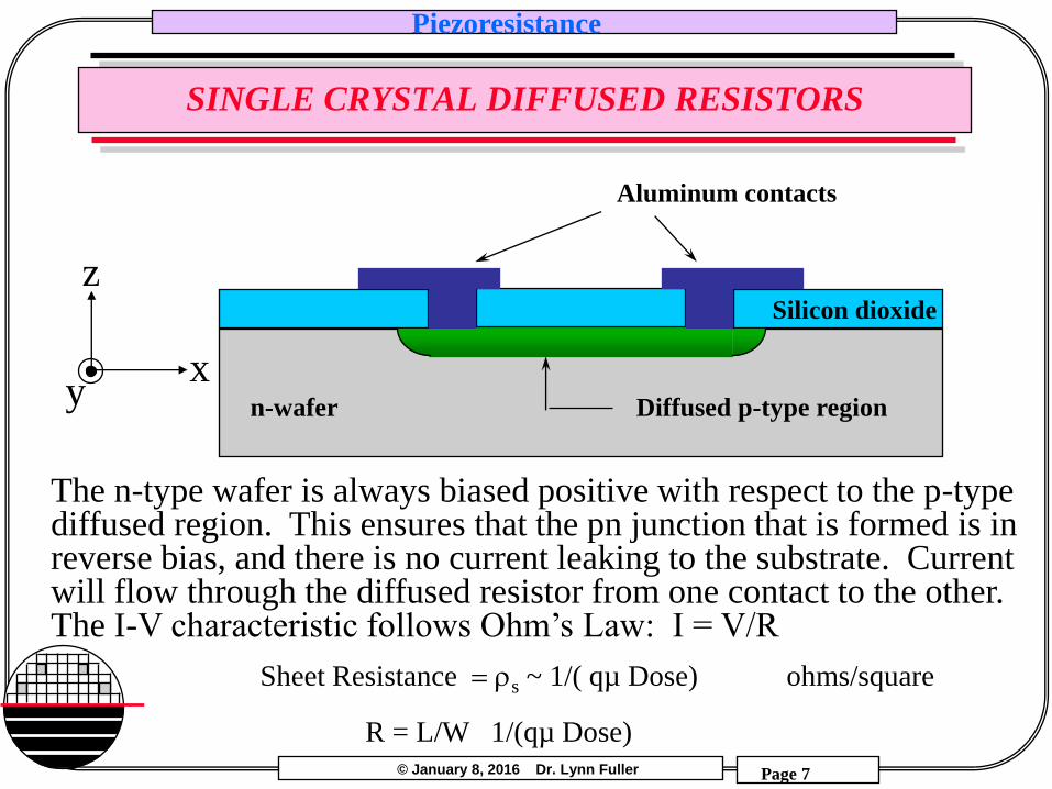
SINGLE CRYSTAL DIFFUSED RESISTORS
Aluminum contacts
The n-type wafer is always biased positive with respect to the p-type diffused region. This ensures that the pn junction that is formed is in reverse bias, and there is no current leaking to the substrate. Current will flow through the diffused resistor from one contact to the other. The I-V characteristic follows Ohm’s Law: I = V/R
n-wafer Diffused p-type region
Silicon dioxide
Sheet Resistance s ~ 1/( qµ Dose) ohms/square R = L/W 1/(qµ Dose)
x y
z

© January 8, 2016 Dr. Lynn Fuller
Piezoresistance
Page 8
Rochester Institute of Technology
Microelectronic Engineering
EXPRESSION FOR RESISTANCE
R = Ro [ 1 + pLxx + pT(yy + zz)]
Ro = (L/W)(1/(qµ(N,T) Dose))
pL is longitudinal piezoresistive coefficient
pT is transverse piezoresistive coefficient
xx is the x directed stress
yy is the y directed stress
zz is the z directed stress

© January 8, 2016 Dr. Lynn Fuller
Piezoresistance
Page 9
Rochester Institute of Technology
Microelectronic Engineering
PIEZORESISTANCE COEFFICIENTS
In the <110> direction
pL (E-11/Pa) pT (E
-11/Pa)
Electrons -31.6 -17.6
holes 71.8 -66.3
In the <100> direction
pL (E-11/Pa) pT (E
-11/Pa)
Electrons -102 53.4
holes 6.6 -1.1
Direction of Carrier Flow
Tensile strain in (100) silicon increases mobility for electrons for flow in <110> direction
Compressive strain in (100) silicon increases mobility for holes for flow in <110> direction
(100) wafer <110> directions
(100) wafer <100> directions

© January 8, 2016 Dr. Lynn Fuller
Piezoresistance
Page 10
Rochester Institute of Technology
Microelectronic Engineering
PIEZORESISTANCE COEFFICIENTS VS DIRECTION
[2]

© January 8, 2016 Dr. Lynn Fuller
Piezoresistance
Page 11
Rochester Institute of Technology
Microelectronic Engineering
PIEZORESISTANCE COEFFICIENTS VS DIRECTION
© January 8, 2016 Dr. Lynn Fuller
Piezoresistance
Page 12
Rochester Institute of Technology
Microelectronic Engineering
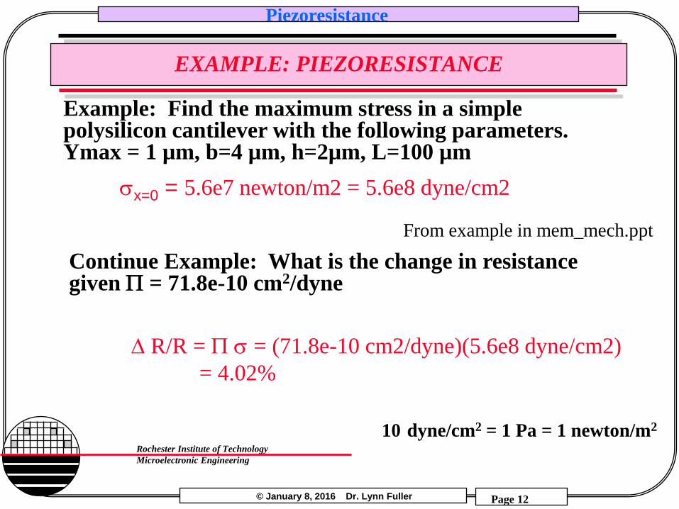
EXAMPLE: PIEZORESISTANCE
Example: Find the maximum stress in a simple polysilicon cantilever with the following parameters. Ymax = 1 µm, b=4 µm, h=2µm, L=100 µm
x=0 = 5.6e7 newton/m2 = 5.6e8 dyne/cm2
From example in mem_mech.ppt
Continue Example: What is the change in resistance given = 71.8e-10 cm2/dyne
R/R = = (71.8e-10 cm2/dyne)(5.6e8 dyne/cm2)
= 4.02%
10 dyne/cm2 = 1 Pa = 1 newton/m2
© January 8, 2016 Dr. Lynn Fuller
Piezoresistance
Page 13
Rochester Institute of Technology
Microelectronic Engineering
SUMMARY FOR MOBILITY / STRAIN
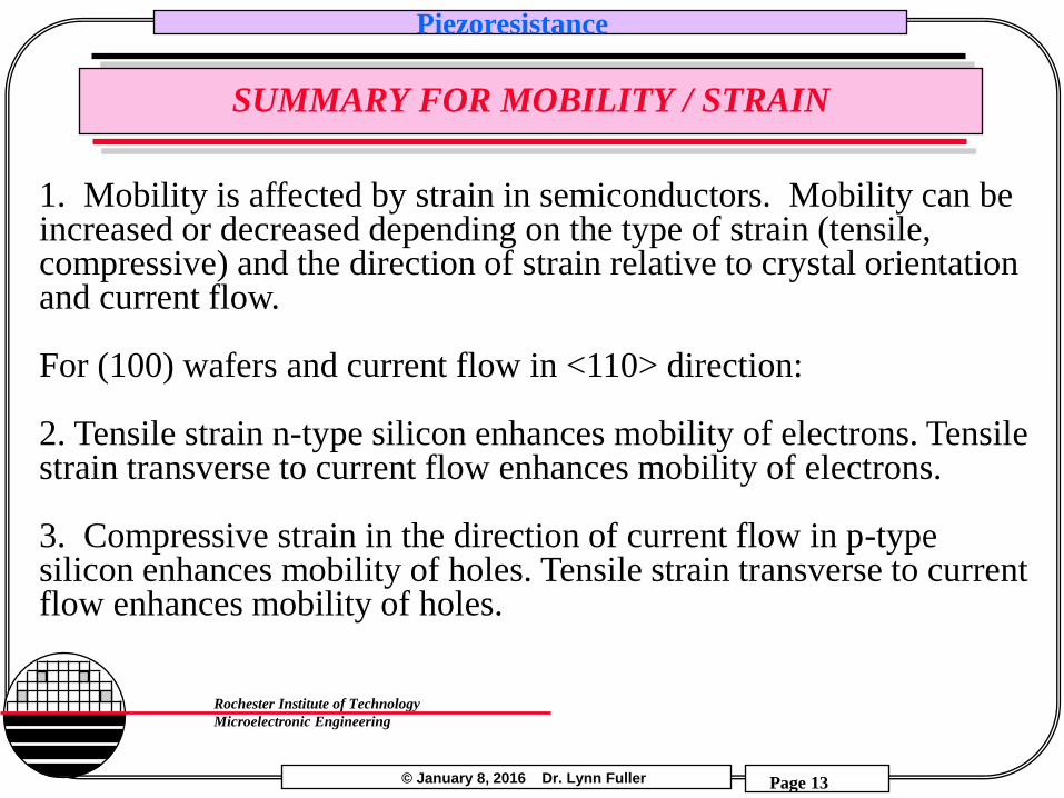
1. Mobility is affected by strain in semiconductors. Mobility can be increased or decreased depending on the type of strain (tensile, compressive) and the direction of strain relative to crystal orientation and current flow. For (100) wafers and current flow in <110> direction: 2. Tensile strain n-type silicon enhances mobility of electrons. Tensile strain transverse to current flow enhances mobility of electrons. 3. Compressive strain in the direction of current flow in p-type silicon enhances mobility of holes. Tensile strain transverse to current flow enhances mobility of holes.

© January 8, 2016 Dr. Lynn Fuller
Piezoresistance
Page 14
Rochester Institute of Technology
Microelectronic Engineering
REFERENCES
1. Charles S. Smith, “Piezoresistance Effect in Germanium and
Silicon,” Physical Review, Vol 94, No.1, April 1, 1954.
2. Y. Kanda, “A graphical representation of the piezoresistance
coefficients in silicon,” Electron Devices, IEEE Transactions on,
vol. 29, no. 1, pp. 64-70, 1982.
3. C. Mazure, and I. Cayrefourcq, "Status of device mobility
enhancement through strained silicon engineering." pp. 1-6.
4. A. A. Barlian, W. T. Park, J. R. Mallon et al., “Review:
Semiconductor Piezoresistance for Microsystems,” Proceedings of
the IEEE, vol. 97, no. 3, pp. 513-552, 2009.

© January 8, 2016 Dr. Lynn Fuller
Piezoresistance
Page 15
Rochester Institute of Technology
Microelectronic Engineering
HOMEWORK - PIEZORESISTANCE
1. If a p-type diffused resistor on a simple cantilever experiences a
tensile stress of 50 MPa what will the % change in resistance be
if the resistor is oriented with its length in the same direction as
the strain?
2. If a p-type diffused resistor on a simple cantilever experiences a
tensile stress of 50 MPa what will the % change in resistance be
if the resistor is oriented with its width in the same direction as
the strain?