pic16f870/871 data sheet
TRANSCRIPT

2003 Microchip Technology Inc. DS30569B
PIC16F870/871Data Sheet
28/40-Pin, 8-Bit CMOSFLASH Microcontrollers
Note the following details of the code protection feature on Microchip devices:
• Microchip products meet the specification contained in their particular Microchip Data Sheet.
• Microchip believes that its family of products is one of the most secure families of its kind on the market today, when used in the intended manner and under normal conditions.
• There are dishonest and possibly illegal methods used to breach the code protection feature. All of these methods, to our knowledge, require using the Microchip products in a manner outside the operating specifications contained in Microchip's Data Sheets. Most likely, the person doing so is engaged in theft of intellectual property.
• Microchip is willing to work with the customer who is concerned about the integrity of their code.
• Neither Microchip nor any other semiconductor manufacturer can guarantee the security of their code. Code protection does not mean that we are guaranteeing the product as “unbreakable.”
Code protection is constantly evolving. We at Microchip are committed to continuously improving the code protection features of ourproducts. Attempts to break microchip’s code protection feature may be a violation of the Digital Millennium Copyright Act. If such actsallow unauthorized access to your software or other copyrighted work, you may have a right to sue for relief under that Act.
Information contained in this publication regarding deviceapplications and the like is intended through suggestion onlyand may be superseded by updates. It is your responsibility toensure that your application meets with your specifications.No representation or warranty is given and no liability isassumed by Microchip Technology Incorporated with respectto the accuracy or use of such information, or infringement ofpatents or other intellectual property rights arising from suchuse or otherwise. Use of Microchip’s products as criticalcomponents in life support systems is not authorized exceptwith express written approval by Microchip. No licenses areconveyed, implicitly or otherwise, under any intellectualproperty rights.
DS30569B-page ii
Trademarks
The Microchip name and logo, the Microchip logo, KEELOQ, MPLAB, PIC, PICmicro, PICSTART, PRO MATE and PowerSmart are registered trademarks of Microchip Technology Incorporated in the U.S.A. and other countries.
FilterLab, microID, MXDEV, MXLAB, PICMASTER, SEEVAL and The Embedded Control Solutions Company are registered trademarks of Microchip Technology Incorporated in the U.S.A.
Accuron, Application Maestro, dsPIC, dsPICDEM, dsPICDEM.net, ECONOMONITOR, FanSense, FlexROM, fuzzyLAB, In-Circuit Serial Programming, ICSP, ICEPIC, microPort, Migratable Memory, MPASM, MPLIB, MPLINK, MPSIM, PICC, PICkit, PICDEM, PICDEM.net, PowerCal, PowerInfo, PowerMate, PowerTool, rfLAB, rfPIC, Select Mode, SmartSensor, SmartShunt, SmartTel and Total Endurance are trademarks of Microchip Technology Incorporated in the U.S.A. and other countries.
Serialized Quick Turn Programming (SQTP) is a service markof Microchip Technology Incorporated in the U.S.A.
All other trademarks mentioned herein are property of theirrespective companies.
© 2003, Microchip Technology Incorporated, Printed in theU.S.A., All Rights Reserved.
Printed on recycled paper.
2003 Microchip Technology Inc.
Microchip received QS-9000 quality system certification for its worldwide headquarters, design and wafer fabrication facilities in Chandler and Tempe, Arizona in July 1999 and Mountain View, California in March 2002. The Company’s quality system processes and procedures are QS-9000 compliant for its PICmicro® 8-bit MCUs, KEELOQ® code hopping devices, Serial EEPROMs, microperipherals, non-volatile memory and analog products. In addition, Microchip’s quality system for the design and manufacture of development systems is ISO 9001 certified.
PIC16F870/87128/40-Pin, 8-Bit CMOS FLASH Microcontrollers
Devices Included in this Data Sheet:
Microcontroller Core Features:
• High performance RISC CPU
• Only 35 single word instructions to learn• All single cycle instructions except for program
branches which are two-cycle• Operating speed: DC - 20 MHz clock input
DC - 200 ns instruction cycle• 2K x 14 words of FLASH Program Memory
128 x 8 bytes of Data Memory (RAM)64 x 8 bytes of EEPROM Data Memory
• Pinout compatible to the PIC16CXXX 28 and 40-pin devices
• Interrupt capability (up to 11 sources)• Eight level deep hardware stack• Direct, Indirect and Relative Addressing modes
• Power-on Reset (POR)• Power-up Timer (PWRT) and
Oscillator Start-up Timer (OST) • Watchdog Timer (WDT) with its own on-chip RC
oscillator for reliable operation• Programmable code protection• Power saving SLEEP mode
• Selectable oscillator options• Low power, high speed CMOS FLASH/EEPROM
technology• Fully static design• In-Circuit Serial Programming (ICSP) via
two pins• Single 5V In-Circuit Serial Programming capability
• In-Circuit Debugging via two pins• Processor read/write access to program memory• Wide operating voltage range: 2.0V to 5.5V
• High Sink/Source Current: 25 mA• Commercial and Industrial temperature ranges• Low power consumption:
- < 1.6 mA typical @ 5V, 4 MHz- 20 µA typical @ 3V, 32 kHz- < 1 µA typical standby current
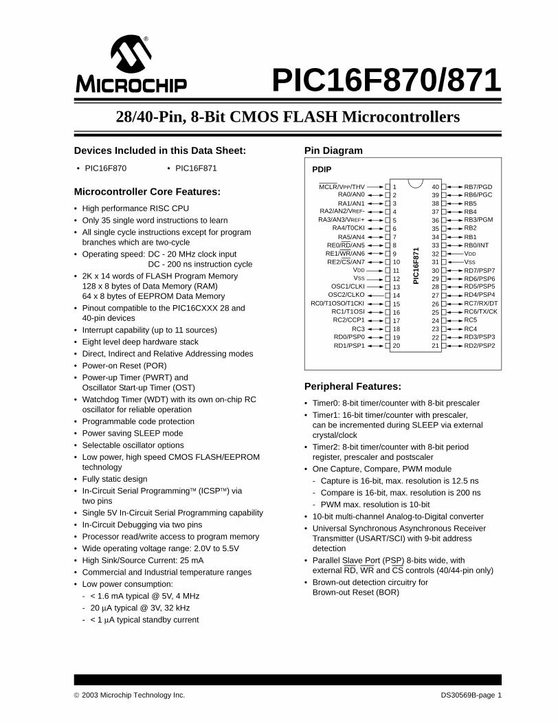
Pin Diagram
Peripheral Features:
• Timer0: 8-bit timer/counter with 8-bit prescaler
• Timer1: 16-bit timer/counter with prescaler,can be incremented during SLEEP via external crystal/clock
• Timer2: 8-bit timer/counter with 8-bit periodregister, prescaler and postscaler
• One Capture, Compare, PWM module
- Capture is 16-bit, max. resolution is 12.5 ns- Compare is 16-bit, max. resolution is 200 ns- PWM max. resolution is 10-bit
• 10-bit multi-channel Analog-to-Digital converter• Universal Synchronous Asynchronous Receiver
Transmitter (USART/SCI) with 9-bit address detection
• Parallel Slave Port (PSP) 8-bits wide, withexternal RD, WR and CS controls (40/44-pin only)
• Brown-out detection circuitry forBrown-out Reset (BOR)
• PIC16F870 • PIC16F871
RB7/PGDRB6/PGCRB5RB4RB3/PGMRB2
RB1RB0/INTVDD
VSS
RD7/PSP7RD6/PSP6RD5/PSP5RD4/PSP4RC7/RX/DTRC6/TX/CKRC5RC4RD3/PSP3RD2/PSP2
MCLR/VPP/THVRA0/AN0
RA1/AN1RA2/AN2/VREF-RA3/AN3/VREF+
RA4/T0CKI
RA5/AN4RE0/RD/AN5RE1/WR/AN6RE2/CS/AN7
VDD
VSS
OSC1/CLKIOSC2/CLKO
RC0/T1OSO/T1CKIRC1/T1OSIRC2/CCP1
RC3RD0/PSP0RD1/PSP1
1234567891011121314151617181920
4039383736353433323130292827262524232221
PIC
16F
871
PDIP
2003 Microchip Technology Inc. DS30569B-page 1
PIC16F870/871
Pin Diagrams
PIC
16F
870
1011
23456
1
87
9
121314 15
1617181920
232425
262728
2221
MCLR/VPP/THVRA0/AN0RA1/AN1
RA2/AN2/VREF-RA3/AN3/VREF+
RA4/T0CKIRA5/AN4
VSS
OSC1/CLKIOSC2/CLKO
RC0/T1OSO/T1CKIRC1/T1OSIRC2/CCP1
RC3
RB7/PGDRB6/PGCRB5RB4RB3/PGMRB2RB1RB0/INTVDD
VSS
RC7/RX/DTRC6/TX/CKRC5RC4
1011121314151617
18 19 20 21 22 23 24 25 26
44
87
6 5 4 3 2 1
27 28
293031323334353637383940414243
9
PIC16F871
RA4/T0CKIRA5/AN4
RE0/RD/AN5
OSC1/CLKIOSC2/CLKO
RC0/T1OSO/T1CK1NC
RE1/WR/AN6RE2/CS/AN7
VDDVSS
RB3/PGMRB2RB1RB0/INTVDDVSSRD7/PSP7RD6/PSP6RD5/PSP5RD4/PSP4RC7/RX/DT
RA
3/A
N3/
VR
EF+
RA
2/A
N2/
VR
EF-
RA
1/A
N1
RA
0/A
N0
MC
LR/V
PP/T
HV
NC
RB
7/P
GD
RB
6/P
GC
RB
5R
B4
NC
NC
RC
6/T
X/C
KR
C5
RC
4R
D3/
PS
P3
RD
2/P
SP
2R
D1/
PS
P1
RD
0/P
SP
0R
C3
RC
2/C
CP
1R
C1/
T1O
SI
1011
23456
1
18 19 20 21 2212 13 14 15
38
87
44 43 42 41 40 3916 17
2930313233
232425262728
36 3435
9
PIC16F871
37
RA
3/A
N3/
VR
EF+
RA
2/A
N2/
VR
EF-
RA
1/A
N1
RA
0/A
N0
MC
LR/V
PP/T
HV
NC
RB
7/P
GD
RB
6/P
GC
RB
5R
B4
NC
RC
6/T
X/C
KR
C5
RC
4R
D3/
PS
P3
RD
2/P
SP
2R
D1/
PS
P1
RD
0/P
SP
0R
C3
RC
2/C
CP
1R
C1/
T1O
SI
NC
NCRC0/T1OSO/T1CKIOSC2/CLKOOSC1/CLKIVSS
VDD
RE2/CS/AN7RE1/WR/AN6RE0/RD/AN5RA5/AN4RA4/T0CKI
RC7/RX/DTRD4/PSP4RD5/PSP5RD6/PSP6RD7/PSP7
VSS
VDD
RB0/INTRB1RB2
RB3/PGM
PLCC
TQFP
DIP, SOIC, SSOP
DS30569B-page 2 2003 Microchip Technology Inc.
PIC16F870/871
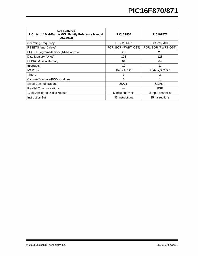
Key FeaturesPICmicroTM Mid-Range MCU Family Reference Manual
(DS33023)PIC16F870 PIC16F871
Operating Frequency DC - 20 MHz DC - 20 MHz
RESETS (and Delays) POR, BOR (PWRT, OST) POR, BOR (PWRT, OST)
FLASH Program Memory (14-bit words) 2K 2K
Data Memory (bytes) 128 128
EEPROM Data Memory 64 64
Interrupts 10 11
I/O Ports Ports A,B,C Ports A,B,C,D,E
Timers 3 3
Capture/Compare/PWM modules 1 1
Serial Communications USART USART
Parallel Communications — PSP
10-bit Analog-to-Digital Module 5 input channels 8 input channels
Instruction Set 35 Instructions 35 Instructions
2003 Microchip Technology Inc. DS30569B-page 3
PIC16F870/871
Table of Contents
1.0 Device Overview .......................................................................................................................................................................... 52.0 Memory Organization ................................................................................................................................................................. 113.0 Data EEPROM and Flash Program Memory.............................................................................................................................. 274.0 I/O Ports ..................................................................................................................................................................................... 335.0 Timer0 Module ........................................................................................................................................................................... 456.0 Timer1 Module ........................................................................................................................................................................... 497.0 Timer2 Module ........................................................................................................................................................................... 538.0 Capture/Compare/PWM Modules .............................................................................................................................................. 559.0 Addressable Universal Synchronous Asynchronous Receiver Transmitter (USART)................................................................ 6110.0 Analog-to-Digital (A/D) Converter Module.................................................................................................................................. 7911.0 Special Features of the CPU...................................................................................................................................................... 8712.0 Instruction Set Summary .......................................................................................................................................................... 10313.0 Development Support............................................................................................................................................................... 11114.0 Electrical Characteristics .......................................................................................................................................................... 11715.0 DC and AC Characteristics Graphs and Tables....................................................................................................................... 13716.0 Packaging Information.............................................................................................................................................................. 149Appendix A: Revision History............................................................................................................................................................. 157Appendix B: Device Differences......................................................................................................................................................... 157Appendix C: Conversion Considerations ........................................................................................................................................... 158Appendix D: Migration from Mid-Range to Enhanced Devices .......................................................................................................... 158Appendix E: Migration from High-End to Enhanced Devices............................................................................................................. 159Index .................................................................................................................................................................................................. 161On-Line Support................................................................................................................................................................................. 167Systems Information and Upgrade Hot Line ...................................................................................................................................... 167Reader Response .............................................................................................................................................................................. 168PIC16F870/871 Product Identification System .................................................................................................................................. 169
TO OUR VALUED CUSTOMERS
It is our intention to provide our valued customers with the best documentation possible to ensure successful use of your Microchipproducts. To this end, we will continue to improve our publications to better suit your needs. Our publications will be refined andenhanced as new volumes and updates are introduced.
If you have any questions or comments regarding this publication, please contact the Marketing Communications Department viaE-mail at [email protected] or fax the Reader Response Form in the back of this data sheet to (480) 792-4150.We welcome your feedback.
Most Current Data SheetTo obtain the most up-to-date version of this data sheet, please register at our Worldwide Web site at:
http://www.microchip.com
You can determine the version of a data sheet by examining its literature number found on the bottom outside corner of any page.The last character of the literature number is the version number, (e.g., DS30000A is version A of document DS30000).
ErrataAn errata sheet, describing minor operational differences from the data sheet and recommended workarounds, may exist for currentdevices. As device/documentation issues become known to us, we will publish an errata sheet. The errata will specify the revisionof silicon and revision of document to which it applies.
To determine if an errata sheet exists for a particular device, please check with one of the following:
• Microchip’s Worldwide Web site; http://www.microchip.com• Your local Microchip sales office (see last page)• The Microchip Corporate Literature Center; U.S. FAX: (480) 792-7277When contacting a sales office or the literature center, please specify which device, revision of silicon and data sheet (includeliterature number) you are using.
Customer Notification SystemRegister on our web site at www.microchip.com/cn to receive the most current information on all of our products.
DS30569B-page 4 2003 Microchip Technology Inc.
PIC16F870/871
1.0 DEVICE OVERVIEW
This document contains device specific information.Additional information may be found in the PICmicroTM
Mid-Range MCU Family Reference Manual(DS33023), which may be obtained from your localMicrochip Sales Representative or downloaded fromthe Microchip web site. The Reference Manual shouldbe considered a complementary document to this datasheet, and is highly recommended reading for a betterunderstanding of the device architecture and operationof the peripheral modules.
There are two devices (PIC16F870 and PIC16F871)covered by this data sheet. The PIC16F870 devicecomes in a 28-pin package and the PIC16F871 devicecomes in a 40-pin package. The 28-pin device does nothave a Parallel Slave Port implemented.
The following two figures are device block diagramssorted by pin number: 28-pin for Figure 1-1 and 40-pinfor Figure 1-2. The 28-pin and 40-pin pinouts are listedin Table 1-1 and Table 1-2, respectively.
FIGURE 1-1: PIC16F870 BLOCK DIAGRAM
FLASHProgramMemory
13 Data Bus 8
14ProgramBus
Instruction reg
Program Counter
8 Level Stack(13-bit)
RAMFile
Registers
Direct Addr 7
RAM Addr (1) 9
Addr MUX
IndirectAddr
FSR reg
STATUS reg
MUX
ALU
W reg
Power-upTimer
OscillatorStart-up Timer
Power-onReset
WatchdogTimer
InstructionDecode &
Control
TimingGeneration
OSC1/CLKIOSC2/CLKO
MCLR VDD, VSS
PORTA
PORTB
PORTC
RA4/T0CKIRA5/AN4
RB0/INT
RC0/T1OSO/T1CKIRC1/T1OSIRC2/CCP1RC3RC4RC5RC6/TX/CKRC7/RX/DT
8
8
Brown-outReset
Note 1: Higher order bits are from the STATUS register.
USARTCCP1
10-bit A/DTimer0 Timer1 Timer2
RA3/AN3/VREF+RA2/AN2/VREF-RA1/AN1RA0/AN0
8
3
Data EEPROM
RB1RB2RB3/PGMRB4RB5RB6/PGCRB7/PGD
Device Program FLASH Data Memory Data EEPROM
PIC16F870 2K 128 Bytes 64 Bytes
In-CircuitDebugger
Low-VoltageProgramming
2003 Microchip Technology Inc. DS30569B-page 5
PIC16F870/871
FIGURE 1-2: PIC16F871 BLOCK DIAGRAM
FLASH
ProgramMemory
13 Data Bus 8
14ProgramBus
Instruction reg
Program Counter
8 Level Stack(13-bit)
RAMFile
Registers
Direct Addr 7
RAM Addr (1) 9
Addr MUX
IndirectAddr
FSR reg
STATUS reg
MUX
ALU
W reg
Power-upTimer
OscillatorStart-up Timer
Power-onReset
WatchdogTimer
InstructionDecode &
Control
TimingGeneration
OSC1/CLKIOSC2/CLKO
MCLR VDD, VSS
PORTA
PORTB
PORTC
PORTD
PORTE
RA4/T0CKIRA5/AN4
RC0/T1OSO/T1CKIRC1/T1OSIRC2/CCP1RC3RC4RC5RC6/TX/CKRC7/RX/DT
RD7/PSP7:RD0/PSP0
RE0/RD/AN5
RE1/WR/AN6
RE2/CS/AN7
8
8
Brown-outReset
Note 1: Higher order bits are from the STATUS register.
USARTCCP1
10-bit A/DTimer0 Timer1 Timer2
RA3/AN3/VREF+RA2/AN2/VREF-RA1/AN1RA0/AN0
8
3
Data EEPROM
RB0/INTRB1RB2RB3/PGMRB4RB5RB6/PGCRB7/PGD
Device Program FLASH Data Memory Data EEPROM
PIC16F871 2K 128 Bytes 64 Bytes
In-CircuitDebugger
Low-VoltageProgramming
Parallel Slave Port
DS30569B-page 6 2003 Microchip Technology Inc.
PIC16F870/871
TABLE 1-1: PIC16F870 PINOUT DESCRIPTIONPin NameDIPPin#
SOICPin#
I/O/PType
BufferType
Description
OSC1/CLKI 9 9 I ST/CMOS(3) Oscillator crystal input/external clock source input.
OSC2/CLKO 10 10 O — Oscillator crystal output. Connects to crystal or resonator in Crystal Oscillator mode. In RC mode, the OSC2 pin outputs CLKO, which has 1/4 the frequency of OSC1, and denotes the instruction cycle rate.
MCLR/VPP/THV 1 1 I/P ST Master Clear (Reset) input or programming voltage input or High Voltage Test mode control. This pin is an active low RESET to the device.
PORTA is a bi-directional I/O port.
RA0/AN0 2 2 I/O TTL RA0 can also be analog input 0.
RA1/AN1 3 3 I/O TTL RA1 can also be analog input 1.
RA2/AN2/VREF- 4 4 I/O TTL RA2 can also be analog input 2 or negative analog referencevoltage.
RA3/AN3/VREF+ 5 5 I/O TTL RA3 can also be analog input 3 or positive analog referencevoltage.
RA4/T0CKI 6 6 I/O ST/OD RA4 can also be the clock input to the Timer0 module. Outputis open drain type.
RA5/AN4 7 7 I/O TTL RA5 can also be analog input 4.
PORTB is a bi-directional I/O port. PORTB can be software programmed for internal weak pull-up on all inputs.
RB0/INT 21 21 I/O TTL/ST(1) RB0 can also be the external interrupt pin.
RB1 22 22 I/O TTL
RB2 23 23 I/O TTL
RB3/PGM 24 24 I/O TTL/ST(1) RB3 can also be the low voltage programming input.
RB4 25 25 I/O TTL Interrupt-on-change pin.
RB5 26 26 I/O TTL Interrupt-on-change pin.
RB6/PGC 27 27 I/O TTL/ST(2) Interrupt-on-change pin or In-Circuit Debugger pin. Serial programming clock.
RB7/PGD 28 28 I/O TTL/ST(2) Interrupt-on-change pin or In-Circuit Debugger pin. Serial programming data.
PORTC is a bi-directional I/O port.
RC0/T1OSO/T1CKI 11 11 I/O ST RC0 can also be the Timer1 oscillator output or Timer1 clockinput.
RC1/T1OSI 12 12 I/O ST RC1 can also be the Timer1 oscillator input.
RC2/CCP1 13 13 I/O ST RC2 can also be the Capture1 input/Compare1 output/PWM1 output.
RC3 14 14 I/O ST
RC4 15 15 I/O ST
RC5 16 16 I/O ST
RC6/TX/CK 17 17 I/O ST RC6 can also be the USART Asynchronous Transmit or Synchronous Clock.
RC7/RX/DT 18 18 I/O ST RC7 can also be the USART Asynchronous Receive or Synchronous Data.
VSS 8, 19 8, 19 P — Ground reference for logic and I/O pins.
VDD 20 20 P — Positive supply for logic and I/O pins.
Legend: I = input O = output I/O = input/output P = powerOD = Open Drain — = Not used TTL = TTL input ST = Schmitt Trigger input
Note 1: This buffer is a Schmitt Trigger input when configured as the external interrupt or LVP mode.2: This buffer is a Schmitt Trigger input when used in Serial Programming mode.3: This buffer is a Schmitt Trigger input when configured in RC Oscillator mode and a CMOS input otherwise.
2003 Microchip Technology Inc. DS30569B-page 7
PIC16F870/871
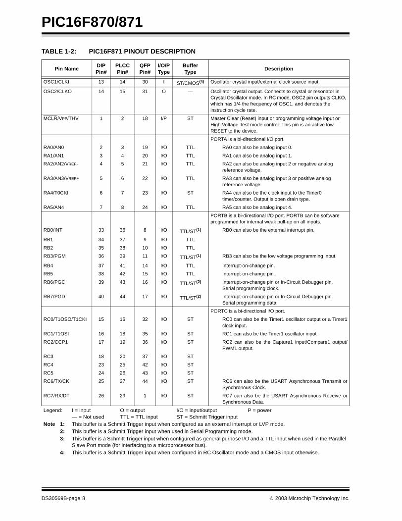
TABLE 1-2: PIC16F871 PINOUT DESCRIPTION
Pin NameDIPPin#
PLCCPin#
QFPPin#
I/O/PType
BufferType
Description
OSC1/CLKI 13 14 30 I ST/CMOS(4) Oscillator crystal input/external clock source input.
OSC2/CLKO 14 15 31 O — Oscillator crystal output. Connects to crystal or resonator in Crystal Oscillator mode. In RC mode, OSC2 pin outputs CLKO, which has 1/4 the frequency of OSC1, and denotes the instruction cycle rate.
MCLR/VPP/THV 1 2 18 I/P ST Master Clear (Reset) input or programming voltage input or High Voltage Test mode control. This pin is an active low RESET to the device.
PORTA is a bi-directional I/O port.
RA0/AN0 2 3 19 I/O TTL RA0 can also be analog input 0.
RA1/AN1 3 4 20 I/O TTL RA1 can also be analog input 1.
RA2/AN2/VREF- 4 5 21 I/O TTL RA2 can also be analog input 2 or negative analog reference voltage.
RA3/AN3/VREF+ 5 6 22 I/O TTL RA3 can also be analog input 3 or positive analog reference voltage.
RA4/T0CKI 6 7 23 I/O ST RA4 can also be the clock input to the Timer0 timer/counter. Output is open drain type.
RA5/AN4 7 8 24 I/O TTL RA5 can also be analog input 4.
PORTB is a bi-directional I/O port. PORTB can be software programmed for internal weak pull-up on all inputs.
RB0/INT 33 36 8 I/O TTL/ST(1) RB0 can also be the external interrupt pin.
RB1 34 37 9 I/O TTL
RB2 35 38 10 I/O TTL
RB3/PGM 36 39 11 I/O TTL/ST(1) RB3 can also be the low voltage programming input.
RB4 37 41 14 I/O TTL Interrupt-on-change pin.
RB5 38 42 15 I/O TTL Interrupt-on-change pin.
RB6/PGC 39 43 16 I/O TTL/ST(2) Interrupt-on-change pin or In-Circuit Debugger pin. Serial programming clock.
RB7/PGD 40 44 17 I/O TTL/ST(2) Interrupt-on-change pin or In-Circuit Debugger pin. Serial programming data.
PORTC is a bi-directional I/O port.
RC0/T1OSO/T1CKI 15 16 32 I/O ST RC0 can also be the Timer1 oscillator output or a Timer1clock input.
RC1/T1OSI 16 18 35 I/O ST RC1 can also be the Timer1 oscillator input.
RC2/CCP1 17 19 36 I/O ST RC2 can also be the Capture1 input/Compare1 output/PWM1 output.
RC3 18 20 37 I/O ST
RC4 23 25 42 I/O ST
RC5 24 26 43 I/O ST
RC6/TX/CK 25 27 44 I/O ST RC6 can also be the USART Asynchronous Transmit orSynchronous Clock.
RC7/RX/DT 26 29 1 I/O ST RC7 can also be the USART Asynchronous Receive orSynchronous Data.
Legend: I = input O = output I/O = input/output P = power— = Not used TTL = TTL input ST = Schmitt Trigger input
Note 1: This buffer is a Schmitt Trigger input when configured as an external interrupt or LVP mode.2: This buffer is a Schmitt Trigger input when used in Serial Programming mode.3: This buffer is a Schmitt Trigger input when configured as general purpose I/O and a TTL input when used in the Parallel
Slave Port mode (for interfacing to a microprocessor bus).4: This buffer is a Schmitt Trigger input when configured in RC Oscillator mode and a CMOS input otherwise.
DS30569B-page 8 2003 Microchip Technology Inc.
PIC16F870/871
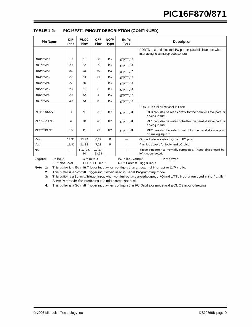
PORTD is a bi-directional I/O port or parallel slave port when interfacing to a microprocessor bus.
RD0/PSP0 19 21 38 I/O ST/TTL(3)
RD1/PSP1 20 22 39 I/O ST/TTL(3)
RD2/PSP2 21 23 40 I/O ST/TTL(3)
RD3/PSP3 22 24 41 I/O ST/TTL(3)
RD4/PSP4 27 30 2 I/O ST/TTL(3)
RD5/PSP5 28 31 3 I/O ST/TTL(3)
RD6/PSP6 29 32 4 I/O ST/TTL(3)
RD7/PSP7 30 33 5 I/O ST/TTL(3)
PORTE is a bi-directional I/O port.
RE0/RD/AN5 8 9 25 I/O ST/TTL(3) RE0 can also be read control for the parallel slave port, oranalog input 5.
RE1/WR/AN6 9 10 26 I/O ST/TTL(3) RE1 can also be write control for the parallel slave port, oranalog input 6.
RE2/CS/AN7 10 11 27 I/O ST/TTL(3) RE2 can also be select control for the parallel slave port,or analog input 7.
VSS 12,31 13,34 6,29 P — Ground reference for logic and I/O pins.
VDD 11,32 12,35 7,28 P — Positive supply for logic and I/O pins.
NC — 1,17,28,40
12,13,33,34
— These pins are not internally connected. These pins should be left unconnected.
TABLE 1-2: PIC16F871 PINOUT DESCRIPTION (CONTINUED)
Pin NameDIPPin#
PLCCPin#
QFPPin#
I/O/PType
BufferType
Description
Legend: I = input O = output I/O = input/output P = power— = Not used TTL = TTL input ST = Schmitt Trigger input
Note 1: This buffer is a Schmitt Trigger input when configured as an external interrupt or LVP mode.2: This buffer is a Schmitt Trigger input when used in Serial Programming mode.3: This buffer is a Schmitt Trigger input when configured as general purpose I/O and a TTL input when used in the Parallel
Slave Port mode (for interfacing to a microprocessor bus).4: This buffer is a Schmitt Trigger input when configured in RC Oscillator mode and a CMOS input otherwise.
2003 Microchip Technology Inc. DS30569B-page 9

PIC16F870/871
NOTES:
DS30569B-page 10 2003 Microchip Technology Inc.
PIC16F870/871
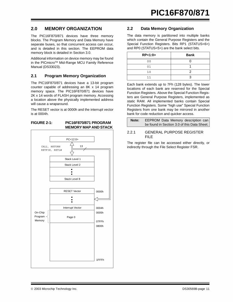
2.0 MEMORY ORGANIZATION
The PIC16F870/871 devices have three memoryblocks. The Program Memory and Data Memory haveseparate buses, so that concurrent access can occur,and is detailed in this section. The EEPROM datamemory block is detailed in Section 3.0.
Additional information on device memory may be foundin the PICmicroTM Mid-Range MCU Family ReferenceManual (DS33023).
2.1 Program Memory Organization
The PIC16F870/871 devices have a 13-bit programcounter capable of addressing an 8K x 14 programmemory space. The PIC16F870/871 devices have2K x 14 words of FLASH program memory. Accessinga location above the physically implemented addresswill cause a wraparound.
The RESET vector is at 0000h and the interrupt vectoris at 0004h.
FIGURE 2-1: PIC16F870/871 PROGRAM MEMORY MAP AND STACK
2.2 Data Memory Organization
The data memory is partitioned into multiple bankswhich contain the General Purpose Registers and theSpecial Function Registers. Bits RP1 (STATUS<6>)and RP0 (STATUS<5>) are the bank select bits.
Each bank extends up to 7Fh (128 bytes). The lowerlocations of each bank are reserved for the SpecialFunction Registers. Above the Special Function Regis-ters are General Purpose Registers, implemented asstatic RAM. All implemented banks contain SpecialFunction Registers. Some “high use” Special FunctionRegisters from one bank may be mirrored in anotherbank for code reduction and quicker access.
2.2.1 GENERAL PURPOSE REGISTER FILE
The register file can be accessed either directly, orindirectly through the File Select Register FSR.
PC<12:0>
13
0000h
0004h
0005h
Stack Level 1
Stack Level 8
RESET Vector
Interrupt Vector
On-Chip
CALL, RETURNRETFIE, RETLW
1FFFh
Stack Level 2
Program
MemoryPage 0
07FFh
0800h
RP<1:0> Bank
00 0
01 1
10 2
11 3
Note: EEPROM Data Memory description canbe found in Section 3.0 of this Data Sheet.
2003 Microchip Technology Inc. DS30569B-page 11
PIC16F870/871
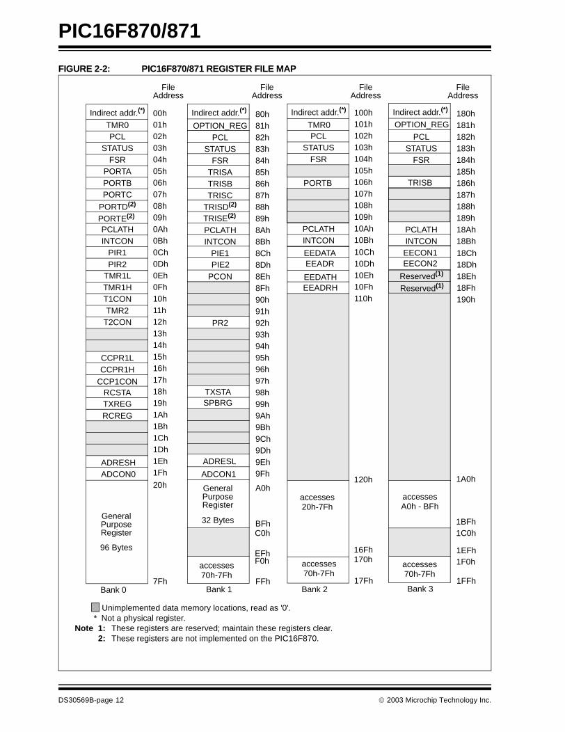
FIGURE 2-2: PIC16F870/871 REGISTER FILE MAP
Indirect addr.(*)
TMR0PCL
STATUSFSR
PORTAPORTBPORTC
PCLATHINTCON
PIR1
TMR1LTMR1HT1CONTMR2
T2CON
CCPR1LCCPR1H
RCSTA
OPTION_REGPCL
STATUSFSR
TRISATRISBTRISC
PCLATHINTCON
PIE1
PCON
PR2
00h01h02h03h04h05h06h07h08h09h0Ah0Bh0Ch0Dh0Eh0Fh10h11h12h13h14h15h16h17h18h19h1Ah1Bh1Ch1Dh1Eh1Fh
80h81h82h83h84h85h86h87h88h89h8Ah8Bh8Ch8Dh8Eh8Fh90h91h92h93h94h95h96h97h98h99h9Ah9Bh9Ch9Dh9Eh9Fh
20h A0h
7Fh FFhBank 0 Bank 1
FileAddress
Indirect addr.(*) Indirect addr.(*)
PCLSTATUS
FSR
PCLATHINTCON
PCLSTATUS
FSR
PCLATHINTCON
100h101h102h103h104h105h106h107h108h109h10Ah10Bh
180h181h182h183h184h185h186h187h188h189h18Ah18Bh
17Fh 1FFhBank 2 Bank 3
Indirect addr.(*)
ADRESL
TMR0 OPTION_REG
PIR2 PIE2
ADRESHADCON0 ADCON1
GeneralPurposeRegister
GeneralPurposeRegister
1EFh1F0h
accessesA0h - BFh
16Fh170haccesses
70h-7Fh
TRISBPORTB
96 Bytes
32 Bytes
10Ch10Dh10Eh10Fh110h
18Ch18Dh18Eh18Fh190h
EEDATAEEADR
EECON1EECON2
EEDATHEEADRH
Reserved(1)
Reserved(1)
Unimplemented data memory locations, read as '0'. * Not a physical register.
Note 1: These registers are reserved; maintain these registers clear.2: These registers are not implemented on the PIC16F870.
120h 1A0h
accesses70h-7Fh
accesses70h-7Fh
accesses20h-7Fh
C0h
EFhF0h
1C0h1BFhBFh
TXREGRCREG
CCP1CONTXSTASPBRG
PORTD(2)
PORTE(2)TRISD(2)
TRISE(2)
FileAddress
FileAddress
FileAddress
DS30569B-page 12 2003 Microchip Technology Inc.
PIC16F870/871
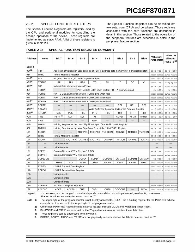
2.2.2 SPECIAL FUNCTION REGISTERS
The Special Function Registers are registers used bythe CPU and peripheral modules for controlling thedesired operation of the device. These registers areimplemented as static RAM. A list of these registers isgiven in Table 2-1.
The Special Function Registers can be classified intotwo sets: core (CPU) and peripheral. Those registersassociated with the core functions are described indetail in this section. Those related to the operation ofthe peripheral features are described in detail in theperipheral feature section.
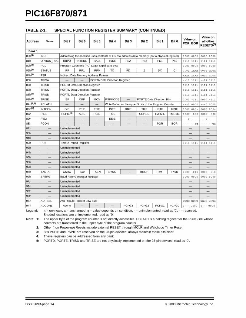
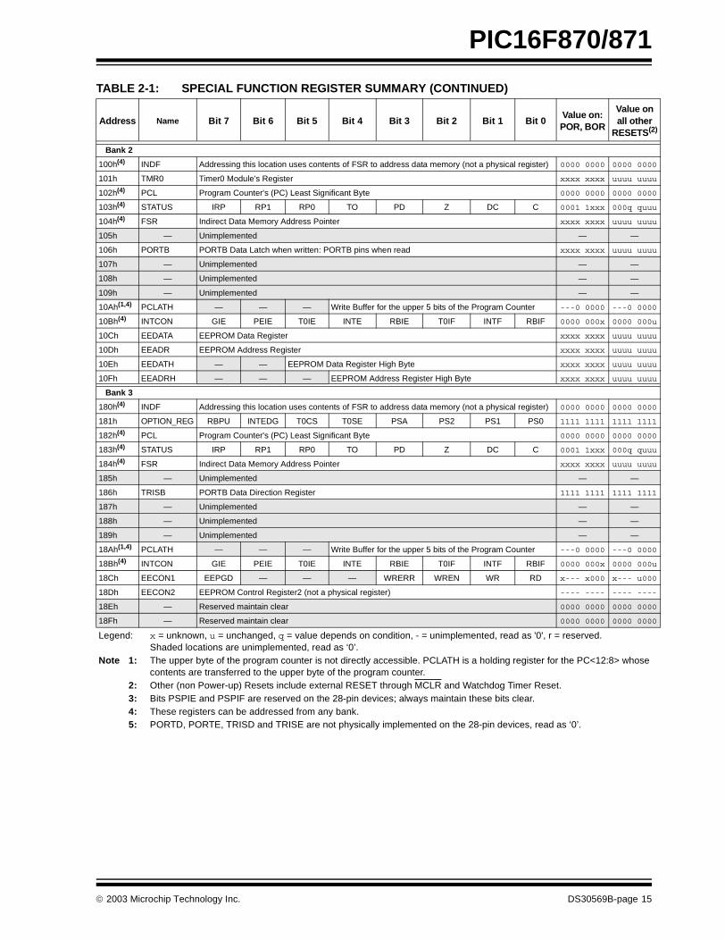
TABLE 2-1: SPECIAL FUNCTION REGISTER SUMMARY
Address Name Bit 7 Bit 6 Bit 5 Bit 4 Bit 3 Bit 2 Bit 1 Bit 0Value on:POR, BOR
Value on all other
RESETS(2)
Bank 0
00h(4) INDF Addressing this location uses contents of FSR to address data memory (not a physical register) 0000 0000 0000 0000
01h TMR0 Timer0 Module’s Register xxxx xxxx uuuu uuuu
02h(4) PCL Program Counter's (PC) Least Significant Byte 0000 0000 0000 0000
03h(4) STATUS IRP RP1 RP0 TO PD Z DC C 0001 1xxx 000q quuu
04h(4) FSR Indirect Data Memory Address Pointer xxxx xxxx uuuu uuuu
05h PORTA — — PORTA Data Latch when written: PORTA pins when read --0x 0000 --0u 0000
06h PORTB PORTB Data Latch when written: PORTB pins when read xxxx xxxx uuuu uuuu
07h PORTC PORTC Data Latch when written: PORTC pins when read xxxx xxxx uuuu uuuu
08h(5) PORTD PORTD Data Latch when written: PORTD pins when read xxxx xxxx uuuu uuuu
09h(5) PORTE — — — — — RE2 RE1 RE0 ---- -xxx ---- -uuu
0Ah(1,4) PCLATH — — — Write Buffer for the upper 5 bits of the Program Counter ---0 0000 ---0 0000
0Bh(4) INTCON GIE PEIE T0IE INTE RBIE T0IF INTF RBIF 0000 000x 0000 000u
0Ch PIR1 PSPIF(3) ADIF RCIF TXIF — CCP1IF TMR2IF TMR1IF 0000 -000 0000 -000
0Dh PIR2 — — — EEIF — — — — ---0 ---- ---0 ----
0Eh TMR1L Holding Register for the Least Significant Byte of the 16-bit TMR1 Register xxxx xxxx uuuu uuuu
0Fh TMR1H Holding Register for the Most Significant Byte of the 16-bit TMR1 Register xxxx xxxx uuuu uuuu
10h T1CON — — T1CKPS1 T1CKPS0 T1OSCEN T1SYNC TMR1CS TMR1ON --00 0000 --uu uuuu
11h TMR2 Timer2 Module’s Register 0000 0000 0000 0000
12h T2CON — TOUTPS3 TOUTPS2 TOUTPS1 TOUTPS0 TMR2ON T2CKPS1 T2CKPS0 -000 0000 -000 0000
13h — Unimplemented — —
14h — Unimplemented — —
15h CCPR1L Capture/Compare/PWM Register1 (LSB) xxxx xxxx uuuu uuuu
16h CCPR1H Capture/Compare/PWM Register1 (MSB) xxxx xxxx uuuu uuuu
17h CCP1CON — — CCP1X CCP1Y CCP1M3 CCP1M2 CCP1M1 CCP1M0 --00 0000 --00 0000
18h RCSTA SPEN RX9 SREN CREN ADDEN FERR OERR RX9D 0000 000x 0000 000x
19h TXREG USART Transmit Data Register 0000 0000 0000 0000
1Ah RCREG USART Receive Data Register 0000 0000 0000 0000
1Bh — Unimplemented — —
1Ch — Unimplemented — —
1Dh — Unimplemented — —
1Eh ADRESH A/D Result Register High Byte xxxx xxxx uuuu uuuu
1Fh ADCON0 ADCS1 ADCS0 CHS2 CHS1 CHS0 GO/DONE — ADON 0000 00-0 0000 00-0
Legend: x = unknown, u = unchanged, q = value depends on condition, - = unimplemented, read as '0', r = reserved. Shaded locations are unimplemented, read as ‘0’.
Note 1: The upper byte of the program counter is not directly accessible. PCLATH is a holding register for the PC<12:8> whose contents are transferred to the upper byte of the program counter.
2: Other (non Power-up) Resets include external RESET through MCLR and Watchdog Timer Reset.3: Bits PSPIE and PSPIF are reserved on the 28-pin devices; always maintain these bits clear.4: These registers can be addressed from any bank.5: PORTD, PORTE, TRISD and TRISE are not physically implemented on the 28-pin devices, read as ‘0’.
2003 Microchip Technology Inc. DS30569B-page 13
PIC16F870/871
Bank 1
80h(4) INDF Addressing this location uses contents of FSR to address data memory (not a physical register) 0000 0000 0000 0000
81h OPTION_REG RBPU INTEDG T0CS T0SE PSA PS2 PS1 PS0 1111 1111 1111 1111
82h(4) PCL Program Counter's (PC) Least Significant Byte 0000 0000 0000 0000
83h(4) STATUS IRP RP1 RP0 TO PD Z DC C 0001 1xxx 000q quuu
84h(4) FSR Indirect Data Memory Address Pointer xxxx xxxx uuuu uuuu
85h TRISA — — PORTA Data Direction Register --11 1111 --11 1111
86h TRISB PORTB Data Direction Register 1111 1111 1111 1111
87h TRISC PORTC Data Direction Register 1111 1111 1111 1111
88h(5) TRISD PORTD Data Direction Register 1111 1111 1111 1111
89h(5) TRISE IBF OBF IBOV PSPMODE — PORTE Data Direction Bits 0000 -111 0000 -111
8Ah(1,4) PCLATH — — — Write Buffer for the upper 5 bits of the Program Counter ---0 0000 ---0 0000
8Bh(4) INTCON GIE PEIE T0IE INTE RBIE T0IF INTF RBIF 0000 000x 0000 000u
8Ch PIE1 PSPIE(3) ADIE RCIE TXIE — CCP1IE TMR2IE TMR1IE 0000 -000 0000 -000
8Dh PIE2 — — — EEIE — — — — ---0 ---- ---0 ----
8Eh PCON — — — — — — POR BOR ---- --qq ---- --uu
8Fh — Unimplemented — —
90h — Unimplemented — —
91h — Unimplemented — —
92h PR2 Timer2 Period Register 1111 1111 1111 1111
93h — Unimplemented — —
94h — Unimplemented — —
95h — Unimplemented — —
96h — Unimplemented — —
97h — Unimplemented — —
98h TXSTA CSRC TX9 TXEN SYNC — BRGH TRMT TX9D 0000 -010 0000 -010
99h SPBRG Baud Rate Generator Register 0000 0000 0000 0000
9Ah — Unimplemented — —
9Bh — Unimplemented — —
9Ch — Unimplemented — —
9Dh — Unimplemented — —
9Eh ADRESL A/D Result Register Low Byte xxxx xxxx uuuu uuuu
9Fh ADCON1 ADFM — — — PCFG3 PCFG2 PCFG1 PCFG0 0--- 0000 0--- 0000
TABLE 2-1: SPECIAL FUNCTION REGISTER SUMMARY (CONTINUED)
Address Name Bit 7 Bit 6 Bit 5 Bit 4 Bit 3 Bit 2 Bit 1 Bit 0Value on:POR, BOR
Value on all other
RESETS(2)
Legend: x = unknown, u = unchanged, q = value depends on condition, - = unimplemented, read as '0', r = reserved. Shaded locations are unimplemented, read as ‘0’.
Note 1: The upper byte of the program counter is not directly accessible. PCLATH is a holding register for the PC<12:8> whose contents are transferred to the upper byte of the program counter.
2: Other (non Power-up) Resets include external RESET through MCLR and Watchdog Timer Reset.3: Bits PSPIE and PSPIF are reserved on the 28-pin devices; always maintain these bits clear.4: These registers can be addressed from any bank.5: PORTD, PORTE, TRISD and TRISE are not physically implemented on the 28-pin devices, read as ‘0’.
DS30569B-page 14 2003 Microchip Technology Inc.
PIC16F870/871
Bank 2
100h(4) INDF Addressing this location uses contents of FSR to address data memory (not a physical register) 0000 0000 0000 0000
101h TMR0 Timer0 Module’s Register xxxx xxxx uuuu uuuu
102h(4) PCL Program Counter's (PC) Least Significant Byte 0000 0000 0000 0000
103h(4) STATUS IRP RP1 RP0 TO PD Z DC C 0001 1xxx 000q quuu
104h(4) FSR Indirect Data Memory Address Pointer xxxx xxxx uuuu uuuu
105h — Unimplemented — —
106h PORTB PORTB Data Latch when written: PORTB pins when read xxxx xxxx uuuu uuuu
107h — Unimplemented — —
108h — Unimplemented — —
109h — Unimplemented — —
10Ah(1,4) PCLATH — — — Write Buffer for the upper 5 bits of the Program Counter ---0 0000 ---0 0000
10Bh(4) INTCON GIE PEIE T0IE INTE RBIE T0IF INTF RBIF 0000 000x 0000 000u
10Ch EEDATA EEPROM Data Register xxxx xxxx uuuu uuuu
10Dh EEADR EEPROM Address Register xxxx xxxx uuuu uuuu
10Eh EEDATH — — EEPROM Data Register High Byte xxxx xxxx uuuu uuuu
10Fh EEADRH — — — EEPROM Address Register High Byte xxxx xxxx uuuu uuuu
Bank 3
180h(4) INDF Addressing this location uses contents of FSR to address data memory (not a physical register) 0000 0000 0000 0000
181h OPTION_REG RBPU INTEDG T0CS T0SE PSA PS2 PS1 PS0 1111 1111 1111 1111
182h(4) PCL Program Counter's (PC) Least Significant Byte 0000 0000 0000 0000
183h(4) STATUS IRP RP1 RP0 TO PD Z DC C 0001 1xxx 000q quuu
184h(4) FSR Indirect Data Memory Address Pointer xxxx xxxx uuuu uuuu
185h — Unimplemented — —
186h TRISB PORTB Data Direction Register 1111 1111 1111 1111
187h — Unimplemented — —
188h — Unimplemented — —
189h — Unimplemented — —
18Ah(1,4) PCLATH — — — Write Buffer for the upper 5 bits of the Program Counter ---0 0000 ---0 0000
18Bh(4) INTCON GIE PEIE T0IE INTE RBIE T0IF INTF RBIF 0000 000x 0000 000u
18Ch EECON1 EEPGD — — — WRERR WREN WR RD x--- x000 x--- u000
18Dh EECON2 EEPROM Control Register2 (not a physical register) ---- ---- ---- ----
18Eh — Reserved maintain clear 0000 0000 0000 0000
18Fh — Reserved maintain clear 0000 0000 0000 0000
TABLE 2-1: SPECIAL FUNCTION REGISTER SUMMARY (CONTINUED)
Address Name Bit 7 Bit 6 Bit 5 Bit 4 Bit 3 Bit 2 Bit 1 Bit 0Value on:POR, BOR
Value on all other
RESETS(2)
Legend: x = unknown, u = unchanged, q = value depends on condition, - = unimplemented, read as '0', r = reserved. Shaded locations are unimplemented, read as ‘0’.
Note 1: The upper byte of the program counter is not directly accessible. PCLATH is a holding register for the PC<12:8> whose contents are transferred to the upper byte of the program counter.
2: Other (non Power-up) Resets include external RESET through MCLR and Watchdog Timer Reset.3: Bits PSPIE and PSPIF are reserved on the 28-pin devices; always maintain these bits clear.4: These registers can be addressed from any bank.5: PORTD, PORTE, TRISD and TRISE are not physically implemented on the 28-pin devices, read as ‘0’.
2003 Microchip Technology Inc. DS30569B-page 15
PIC16F870/871
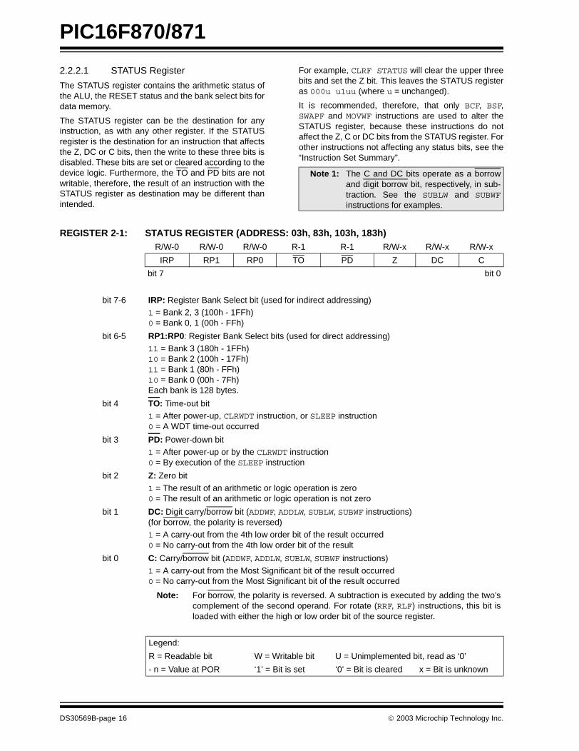
2.2.2.1 STATUS Register
The STATUS register contains the arithmetic status ofthe ALU, the RESET status and the bank select bits fordata memory.
The STATUS register can be the destination for anyinstruction, as with any other register. If the STATUSregister is the destination for an instruction that affectsthe Z, DC or C bits, then the write to these three bits isdisabled. These bits are set or cleared according to thedevice logic. Furthermore, the TO and PD bits are notwritable, therefore, the result of an instruction with theSTATUS register as destination may be different thanintended.
For example, CLRF STATUS will clear the upper threebits and set the Z bit. This leaves the STATUS registeras 000u u1uu (where u = unchanged).
It is recommended, therefore, that only BCF, BSF,SWAPF and MOVWF instructions are used to alter theSTATUS register, because these instructions do notaffect the Z, C or DC bits from the STATUS register. Forother instructions not affecting any status bits, see the“Instruction Set Summary”.
REGISTER 2-1: STATUS REGISTER (ADDRESS: 03h, 83h, 103h, 183h)
Note 1: The C and DC bits operate as a borrowand digit borrow bit, respectively, in sub-traction. See the SUBLW and SUBWFinstructions for examples.
R/W-0 R/W-0 R/W-0 R-1 R-1 R/W-x R/W-x R/W-x
IRP RP1 RP0 TO PD Z DC C
bit 7 bit 0
bit 7-6 IRP: Register Bank Select bit (used for indirect addressing)1 = Bank 2, 3 (100h - 1FFh)0 = Bank 0, 1 (00h - FFh)
bit 6-5 RP1:RP0: Register Bank Select bits (used for direct addressing)
11 = Bank 3 (180h - 1FFh)10 = Bank 2 (100h - 17Fh)11 = Bank 1 (80h - FFh)10 = Bank 0 (00h - 7Fh)Each bank is 128 bytes.
bit 4 TO: Time-out bit1 = After power-up, CLRWDT instruction, or SLEEP instruction0 = A WDT time-out occurred
bit 3 PD: Power-down bit1 = After power-up or by the CLRWDT instruction0 = By execution of the SLEEP instruction
bit 2 Z: Zero bit
1 = The result of an arithmetic or logic operation is zero0 = The result of an arithmetic or logic operation is not zero
bit 1 DC: Digit carry/borrow bit (ADDWF, ADDLW, SUBLW, SUBWF instructions)(for borrow, the polarity is reversed)1 = A carry-out from the 4th low order bit of the result occurred0 = No carry-out from the 4th low order bit of the result
bit 0 C: Carry/borrow bit (ADDWF, ADDLW, SUBLW, SUBWF instructions)
1 = A carry-out from the Most Significant bit of the result occurred0 = No carry-out from the Most Significant bit of the result occurred
Note: For borrow, the polarity is reversed. A subtraction is executed by adding the two’scomplement of the second operand. For rotate (RRF, RLF) instructions, this bit isloaded with either the high or low order bit of the source register.
Legend:
R = Readable bit W = Writable bit U = Unimplemented bit, read as ‘0’
- n = Value at POR ‘1’ = Bit is set ‘0’ = Bit is cleared x = Bit is unknown
DS30569B-page 16 2003 Microchip Technology Inc.
PIC16F870/871
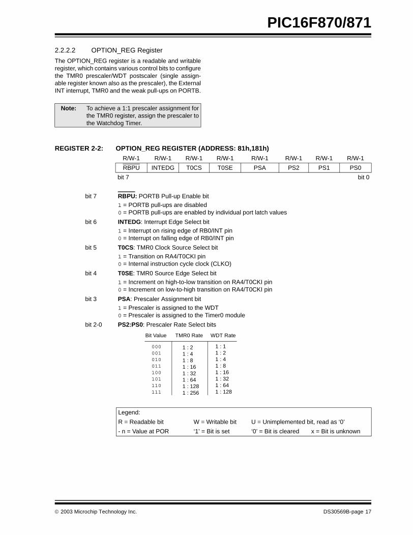
2.2.2.2 OPTION_REG Register
The OPTION_REG register is a readable and writableregister, which contains various control bits to configurethe TMR0 prescaler/WDT postscaler (single assign-able register known also as the prescaler), the ExternalINT interrupt, TMR0 and the weak pull-ups on PORTB.
REGISTER 2-2: OPTION_REG REGISTER (ADDRESS: 81h,181h)
Note: To achieve a 1:1 prescaler assignment forthe TMR0 register, assign the prescaler tothe Watchdog Timer.
R/W-1 R/W-1 R/W-1 R/W-1 R/W-1 R/W-1 R/W-1 R/W-1
RBPU INTEDG T0CS T0SE PSA PS2 PS1 PS0
bit 7 bit 0
bit 7 RBPU: PORTB Pull-up Enable bit1 = PORTB pull-ups are disabled0 = PORTB pull-ups are enabled by individual port latch values
bit 6 INTEDG: Interrupt Edge Select bit1 = Interrupt on rising edge of RB0/INT pin0 = Interrupt on falling edge of RB0/INT pin
bit 5 T0CS: TMR0 Clock Source Select bit
1 = Transition on RA4/T0CKI pin0 = Internal instruction cycle clock (CLKO)
bit 4 T0SE: TMR0 Source Edge Select bit1 = Increment on high-to-low transition on RA4/T0CKI pin0 = Increment on low-to-high transition on RA4/T0CKI pin
bit 3 PSA: Prescaler Assignment bit1 = Prescaler is assigned to the WDT0 = Prescaler is assigned to the Timer0 module
bit 2-0 PS2:PS0: Prescaler Rate Select bits
Legend:
R = Readable bit W = Writable bit U = Unimplemented bit, read as ‘0’
- n = Value at POR ‘1’ = Bit is set ‘0’ = Bit is cleared x = Bit is unknown
000001010011100101110111
1 : 21 : 41 : 81 : 161 : 321 : 641 : 1281 : 256
1 : 11 : 21 : 41 : 81 : 161 : 321 : 641 : 128
Bit Value TMR0 Rate WDT Rate
2003 Microchip Technology Inc. DS30569B-page 17
PIC16F870/871
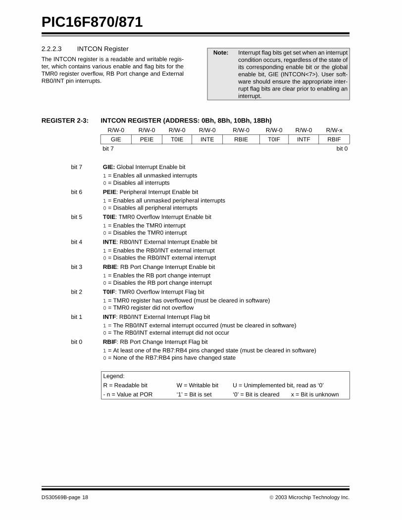
2.2.2.3 INTCON Register
The INTCON register is a readable and writable regis-ter, which contains various enable and flag bits for theTMR0 register overflow, RB Port change and ExternalRB0/INT pin interrupts.
REGISTER 2-3: INTCON REGISTER (ADDRESS: 0Bh, 8Bh, 10Bh, 18Bh)
Note: Interrupt flag bits get set when an interruptcondition occurs, regardless of the state ofits corresponding enable bit or the globalenable bit, GIE (INTCON<7>). User soft-ware should ensure the appropriate inter-rupt flag bits are clear prior to enabling aninterrupt.
R/W-0 R/W-0 R/W-0 R/W-0 R/W-0 R/W-0 R/W-0 R/W-x
GIE PEIE T0IE INTE RBIE T0IF INTF RBIF
bit 7 bit 0
bit 7 GIE: Global Interrupt Enable bit1 = Enables all unmasked interrupts0 = Disables all interrupts
bit 6 PEIE: Peripheral Interrupt Enable bit1 = Enables all unmasked peripheral interrupts0 = Disables all peripheral interrupts
bit 5 T0IE: TMR0 Overflow Interrupt Enable bit
1 = Enables the TMR0 interrupt0 = Disables the TMR0 interrupt
bit 4 INTE: RB0/INT External Interrupt Enable bit1 = Enables the RB0/INT external interrupt0 = Disables the RB0/INT external interrupt
bit 3 RBIE: RB Port Change Interrupt Enable bit1 = Enables the RB port change interrupt0 = Disables the RB port change interrupt
bit 2 T0IF: TMR0 Overflow Interrupt Flag bit
1 = TMR0 register has overflowed (must be cleared in software)0 = TMR0 register did not overflow
bit 1 INTF: RB0/INT External Interrupt Flag bit1 = The RB0/INT external interrupt occurred (must be cleared in software)0 = The RB0/INT external interrupt did not occur
bit 0 RBIF: RB Port Change Interrupt Flag bit1 = At least one of the RB7:RB4 pins changed state (must be cleared in software)0 = None of the RB7:RB4 pins have changed state
Legend:
R = Readable bit W = Writable bit U = Unimplemented bit, read as ‘0’
- n = Value at POR ‘1’ = Bit is set ‘0’ = Bit is cleared x = Bit is unknown
DS30569B-page 18 2003 Microchip Technology Inc.
PIC16F870/871
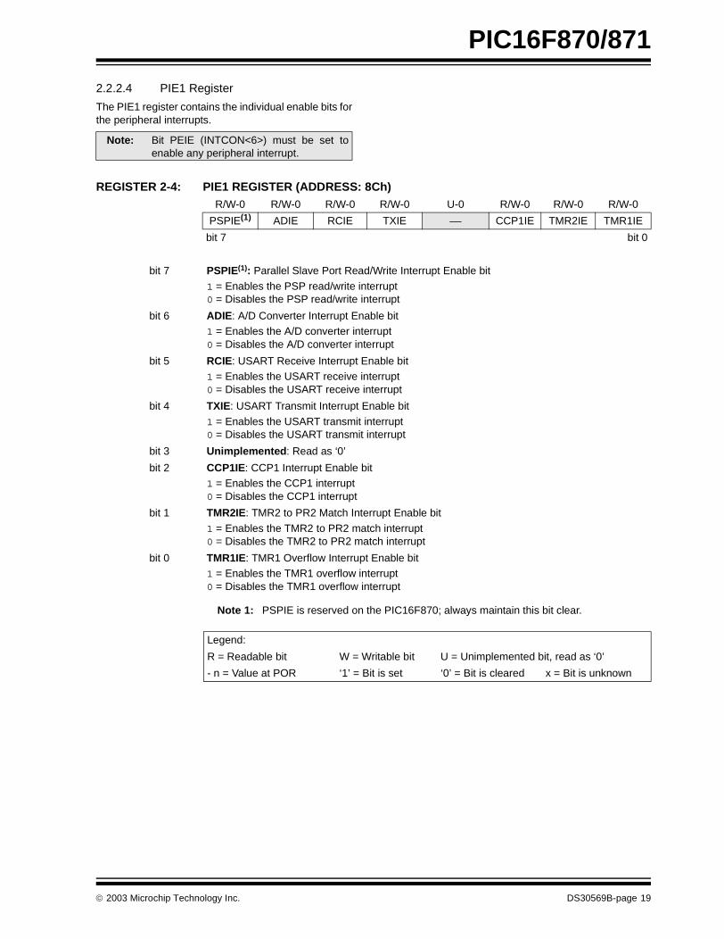
2.2.2.4 PIE1 Register
The PIE1 register contains the individual enable bits forthe peripheral interrupts.
REGISTER 2-4: PIE1 REGISTER (ADDRESS: 8Ch)
Note: Bit PEIE (INTCON<6>) must be set toenable any peripheral interrupt.
R/W-0 R/W-0 R/W-0 R/W-0 U-0 R/W-0 R/W-0 R/W-0
PSPIE(1) ADIE RCIE TXIE CCP1IE TMR2IE TMR1IE
bit 7 bit 0
bit 7 PSPIE(1): Parallel Slave Port Read/Write Interrupt Enable bit
1 = Enables the PSP read/write interrupt0 = Disables the PSP read/write interrupt
bit 6 ADIE: A/D Converter Interrupt Enable bit1 = Enables the A/D converter interrupt0 = Disables the A/D converter interrupt
bit 5 RCIE: USART Receive Interrupt Enable bit1 = Enables the USART receive interrupt0 = Disables the USART receive interrupt
bit 4 TXIE: USART Transmit Interrupt Enable bit
1 = Enables the USART transmit interrupt0 = Disables the USART transmit interrupt
bit 3 Unimplemented: Read as ‘0’
bit 2 CCP1IE: CCP1 Interrupt Enable bit1 = Enables the CCP1 interrupt0 = Disables the CCP1 interrupt
bit 1 TMR2IE: TMR2 to PR2 Match Interrupt Enable bit
1 = Enables the TMR2 to PR2 match interrupt0 = Disables the TMR2 to PR2 match interrupt
bit 0 TMR1IE: TMR1 Overflow Interrupt Enable bit1 = Enables the TMR1 overflow interrupt0 = Disables the TMR1 overflow interrupt
Note 1: PSPIE is reserved on the PIC16F870; always maintain this bit clear.
Legend:
R = Readable bit W = Writable bit U = Unimplemented bit, read as ‘0’
- n = Value at POR ‘1’ = Bit is set ‘0’ = Bit is cleared x = Bit is unknown
2003 Microchip Technology Inc. DS30569B-page 19
PIC16F870/871
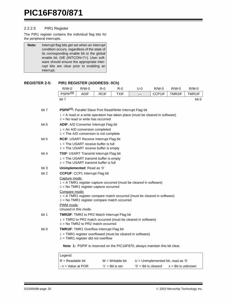
2.2.2.5 PIR1 Register
The PIR1 register contains the individual flag bits forthe peripheral interrupts.
REGISTER 2-5: PIR1 REGISTER (ADDRESS: 0Ch)
Note: Interrupt flag bits get set when an interruptcondition occurs, regardless of the state ofits corresponding enable bit or the globalenable bit, GIE (INTCON<7>). User soft-ware should ensure the appropriate inter-rupt bits are clear prior to enabling aninterrupt.
R/W-0 R/W-0 R-0 R-0 U-0 R/W-0 R/W-0 R/W-0
PSPIF(1) ADIF RCIF TXIF CCP1IF TMR2IF TMR1IF
bit 7 bit 0
bit 7 PSPIF(1): Parallel Slave Port Read/Write Interrupt Flag bit
1 = A read or a write operation has taken place (must be cleared in software)0 = No read or write has occurred
bit 6 ADIF: A/D Converter Interrupt Flag bit1 = An A/D conversion completed0 = The A/D conversion is not complete
bit 5 RCIF: USART Receive Interrupt Flag bit1 = The USART receive buffer is full0 = The USART receive buffer is empty
bit 4 TXIF: USART Transmit Interrupt Flag bit
1 = The USART transmit buffer is empty0 = The USART transmit buffer is full
bit 3 Unimplemented: Read as ‘0’
bit 2 CCP1IF: CCP1 Interrupt Flag bitCapture mode:1 = A TMR1 register capture occurred (must be cleared in software)0 = No TMR1 register capture occurred
Compare mode:1 = A TMR1 register compare match occurred (must be cleared in software)0 = No TMR1 register compare match occurredPWM mode:Unused in this mode.
bit 1 TMR2IF: TMR2 to PR2 Match Interrupt Flag bit1 = TMR2 to PR2 match occurred (must be cleared in software)0 = No TMR2 to PR2 match occurred
bit 0 TMR1IF: TMR1 Overflow Interrupt Flag bit
1 = TMR1 register overflowed (must be cleared in software)0 = TMR1 register did not overflow
Note 1: PSPIF is reserved on the PIC16F870; always maintain this bit clear.
Legend:
R = Readable bit W = Writable bit U = Unimplemented bit, read as ‘0’
- n = Value at POR ‘1’ = Bit is set ‘0’ = Bit is cleared x = Bit is unknown
DS30569B-page 20 2003 Microchip Technology Inc.
PIC16F870/871
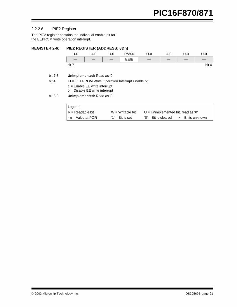
2.2.2.6 PIE2 Register
The PIE2 register contains the individual enable bit forthe EEPROM write operation interrupt.
REGISTER 2-6: PIE2 REGISTER (ADDRESS: 8Dh) U-0 U-0 U-0 R/W-0 U-0 U-0 U-0 U-0
— — — EEIE — — — —
bit 7 bit 0
bit 7-5 Unimplemented: Read as '0'
bit 4 EEIE: EEPROM Write Operation Interrupt Enable bit1 = Enable EE write interrupt0 = Disable EE write interrupt
bit 3-0 Unimplemented: Read as '0'
Legend:
R = Readable bit W = Writable bit U = Unimplemented bit, read as ‘0’
- n = Value at POR ‘1’ = Bit is set ‘0’ = Bit is cleared x = Bit is unknown
2003 Microchip Technology Inc. DS30569B-page 21
PIC16F870/871
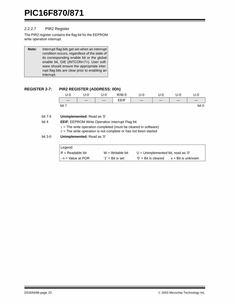
2.2.2.7 PIR2 Register
The PIR2 register contains the flag bit for the EEPROMwrite operation interrupt.
.
REGISTER 2-7: PIR2 REGISTER (ADDRESS: 0Dh)
Note: Interrupt flag bits get set when an interruptcondition occurs, regardless of the state ofits corresponding enable bit or the globalenable bit, GIE (INTCON<7>). User soft-ware should ensure the appropriate inter-rupt flag bits are clear prior to enabling aninterrupt.
U-0 U-0 U-0 R/W-0 U-0 U-0 U-0 U-0
— — — EEIF — — — —
bit 7 bit 0
bit 7-5 Unimplemented: Read as '0'
bit 4 EEIF: EEPROM Write Operation Interrupt Flag bit
1 = The write operation completed (must be cleared in software)0 = The write operation is not complete or has not been started
bit 3-0 Unimplemented: Read as '0'
Legend:
R = Readable bit W = Writable bit U = Unimplemented bit, read as ‘0’
- n = Value at POR ‘1’ = Bit is set ‘0’ = Bit is cleared x = Bit is unknown
DS30569B-page 22 2003 Microchip Technology Inc.
PIC16F870/871
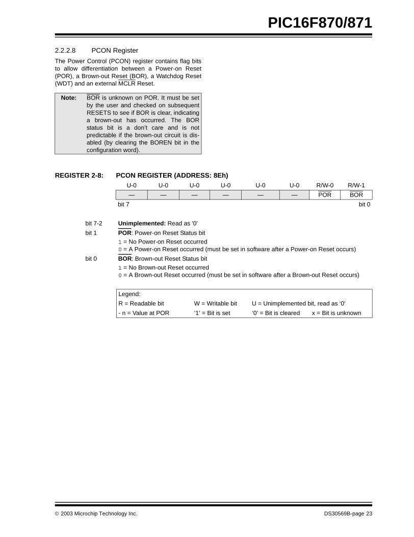
2.2.2.8 PCON Register
The Power Control (PCON) register contains flag bitsto allow differentiation between a Power-on Reset(POR), a Brown-out Reset (BOR), a Watchdog Reset(WDT) and an external MCLR Reset.
REGISTER 2-8: PCON REGISTER (ADDRESS: 8Eh)
Note: BOR is unknown on POR. It must be setby the user and checked on subsequentRESETS to see if BOR is clear, indicatinga brown-out has occurred. The BORstatus bit is a don’t care and is notpredictable if the brown-out circuit is dis-abled (by clearing the BOREN bit in theconfiguration word).
U-0 U-0 U-0 U-0 U-0 U-0 R/W-0 R/W-1
— — — — — — POR BOR
bit 7 bit 0
bit 7-2 Unimplemented: Read as '0'
bit 1 POR: Power-on Reset Status bit1 = No Power-on Reset occurred0 = A Power-on Reset occurred (must be set in software after a Power-on Reset occurs)
bit 0 BOR: Brown-out Reset Status bit
1 = No Brown-out Reset occurred0 = A Brown-out Reset occurred (must be set in software after a Brown-out Reset occurs)
Legend:
R = Readable bit W = Writable bit U = Unimplemented bit, read as ‘0’
- n = Value at POR ‘1’ = Bit is set ‘0’ = Bit is cleared x = Bit is unknown
2003 Microchip Technology Inc. DS30569B-page 23
PIC16F870/871
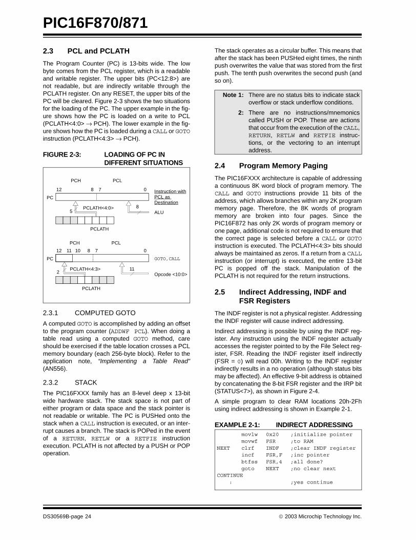
2.3 PCL and PCLATH
The Program Counter (PC) is 13-bits wide. The lowbyte comes from the PCL register, which is a readableand writable register. The upper bits (PC<12:8>) arenot readable, but are indirectly writable through thePCLATH register. On any RESET, the upper bits of thePC will be cleared. Figure 2-3 shows the two situationsfor the loading of the PC. The upper example in the fig-ure shows how the PC is loaded on a write to PCL(PCLATH<4:0> → PCH). The lower example in the fig-ure shows how the PC is loaded during a CALL or GOTOinstruction (PCLATH<4:3> → PCH).
FIGURE 2-3: LOADING OF PC IN DIFFERENT SITUATIONS
2.3.1 COMPUTED GOTO
A computed GOTO is accomplished by adding an offsetto the program counter (ADDWF PCL). When doing atable read using a computed GOTO method, careshould be exercised if the table location crosses a PCLmemory boundary (each 256-byte block). Refer to theapplication note, “Implementing a Table Read"(AN556).
2.3.2 STACK
The PIC16FXXX family has an 8-level deep x 13-bitwide hardware stack. The stack space is not part ofeither program or data space and the stack pointer isnot readable or writable. The PC is PUSHed onto thestack when a CALL instruction is executed, or an inter-rupt causes a branch. The stack is POPed in the eventof a RETURN, RETLW or a RETFIE instructionexecution. PCLATH is not affected by a PUSH or POPoperation.
The stack operates as a circular buffer. This means thatafter the stack has been PUSHed eight times, the ninthpush overwrites the value that was stored from the firstpush. The tenth push overwrites the second push (andso on).
2.4 Program Memory Paging
The PIC16FXXX architecture is capable of addressinga continuous 8K word block of program memory. TheCALL and GOTO instructions provide 11 bits of theaddress, which allows branches within any 2K programmemory page. Therefore, the 8K words of programmemory are broken into four pages. Since thePIC16F872 has only 2K words of program memory orone page, additional code is not required to ensure thatthe correct page is selected before a CALL or GOTOinstruction is executed. The PCLATH<4:3> bits shouldalways be maintained as zeros. If a return from a CALLinstruction (or interrupt) is executed, the entire 13-bitPC is popped off the stack. Manipulation of thePCLATH is not required for the return instructions.
2.5 Indirect Addressing, INDF and FSR Registers
The INDF register is not a physical register. Addressingthe INDF register will cause indirect addressing.
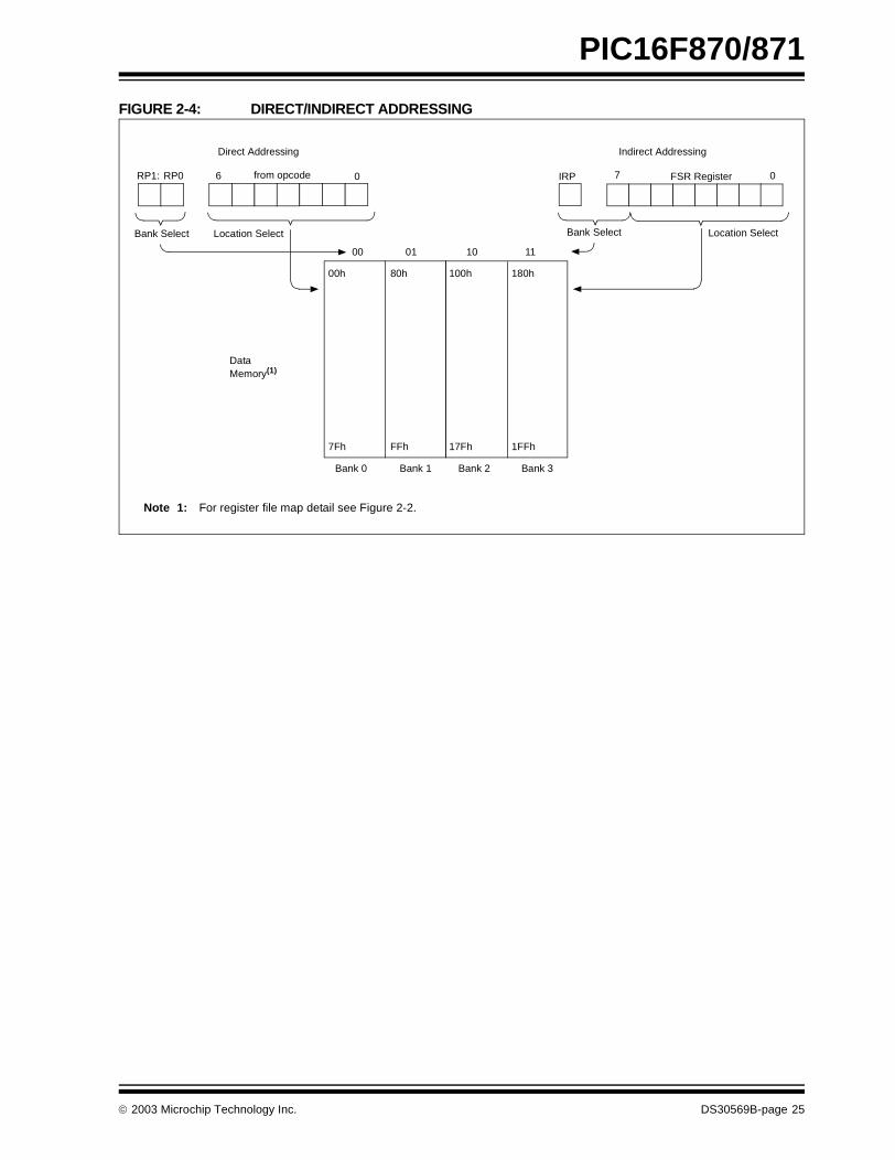
Indirect addressing is possible by using the INDF reg-ister. Any instruction using the INDF register actuallyaccesses the register pointed to by the File Select reg-ister, FSR. Reading the INDF register itself indirectly(FSR = 0) will read 00h. Writing to the INDF registerindirectly results in a no operation (although status bitsmay be affected). An effective 9-bit address is obtainedby concatenating the 8-bit FSR register and the IRP bit(STATUS<7>), as shown in Figure 2-4.
A simple program to clear RAM locations 20h-2Fhusing indirect addressing is shown in Example 2-1.
EXAMPLE 2-1: INDIRECT ADDRESSING
PC
12 8 7 0
5PCLATH<4:0>
PCLATH
Instruction with
ALU
GOTO,CALL
Opcode <10:0>
8
PC
12 11 10 0
11PCLATH<4:3>
PCH PCL
8 7
2
PCLATH
PCH PCL
PCL as Destination
Note 1: There are no status bits to indicate stackoverflow or stack underflow conditions.
2: There are no instructions/mnemonicscalled PUSH or POP. These are actionsthat occur from the execution of the CALL,RETURN, RETLW and RETFIE instruc-tions, or the vectoring to an interruptaddress.
movlw 0x20 ;initialize pointermovwf FSR ;to RAM
NEXT clrf INDF ;clear INDF registerincf FSR,F ;inc pointerbtfss FSR,4 ;all done? goto NEXT ;no clear next
CONTINUE: ;yes continue
DS30569B-page 24 2003 Microchip Technology Inc.
PIC16F870/871
FIGURE 2-4: DIRECT/INDIRECT ADDRESSING
Note 1: For register file map detail see Figure 2-2.
DataMemory(1)
Indirect AddressingDirect Addressing
Bank Select Location Select
RP1: RP0 6 0from opcode IRP FSR Register7 0
Bank Select Location Select
00 01 10 11
Bank 0 Bank 1 Bank 2 Bank 3
FFh
80h
7Fh
00h
17Fh
100h
1FFh
180h
2003 Microchip Technology Inc. DS30569B-page 25

PIC16F870/871
NOTES:
DS30569B-page 26 2003 Microchip Technology Inc.
PIC16F870/871
3.0 DATA EEPROM AND FLASH PROGRAM MEMORY
The Data EEPROM and FLASH Program Memory arereadable and writable during normal operation over theentire VDD range. A bulk erase operation may not beissued from user code (which includes removing codeprotection). The data memory is not directly mapped inthe register file space. Instead, it is indirectly addressedthrough the Special Function Registers (SFR).
There are six SFRs used to read and write the programand data EEPROM memory. These registers are:
• EECON1• EECON2
• EEDATA• EEDATH• EEADR
• EEADRH
The EEPROM data memory allows byte read and write.When interfacing to the data memory block, EEDATAholds the 8-bit data for read/write and EEADR holds theaddress of the EEPROM location being accessed. Theregisters EEDATH and EEADRH are not used for dataEEPROM access. The PIC16F870/871 devices have64 bytes of data EEPROM with an address range from0h to 3Fh.
The EEPROM data memory is rated for high erase/write cycles. The write time is controlled by an on-chiptimer. The write time will vary with voltage and temper-ature, as well as from chip-to-chip. Please refer to thespecifications for exact limits.
The program memory allows word reads and writes.Program memory access allows for checksum calcula-tion and calibration table storage. A byte or word writeautomatically erases the location and writes the newdata (erase before write). Writing to program memorywill cease operation until the write is complete. The pro-gram memory cannot be accessed during the write,therefore code cannot execute. During the write opera-tion, the oscillator continues to clock the peripherals,and therefore, they continue to operate. Interruptevents will be detected and essentially “queued” untilthe write is completed. When the write completes, thenext instruction in the pipeline is executed and thebranch to the interrupt vector address will occur.
When interfacing to the program memory block, theEEDATH:EEDATA registers form a two-byte word,which holds the 14-bit data for read/write. TheEEADRH:EEADR registers form a two-byte word,which holds the 13-bit address of the FLASH locationbeing accessed. The PIC16F870/871 devices have2K words of program FLASH with an address rangefrom 0h to 7FFh. The unused upper bits in both theEEDATH and EEDATA registers all read as ‘0’s.
The value written to program memory does not need tobe a valid instruction. Therefore, up to 14-bit numberscan be stored in memory for use as calibration param-eters, serial numbers, packed 7-bit ASCII, etc. Execut-ing a program memory location containing data thatforms an invalid instruction results in a NOP.
3.1 EEADR
The address registers can address up to a maximum of256 bytes of data EEPROM or up to a maximum of8K words of program FLASH. However, thePIC16F870/871 have 64 bytes of data EEPROM and2K words of program FLASH.
When selecting a program address value, the MSByteof the address is written to the EEADRH register andthe LSByte is written to the EEADR register. Whenselecting a data address value, only the LSByte of theaddress is written to the EEADR register.
On the PIC16F870/871 devices, the upper two bits ofthe EEADR must always be cleared to prevent inad-vertent access to the wrong location in data EEPROM.This also applies to the program memory. The upperfive MSbits of EEADRH must always be clear duringprogram FLASH access.
3.2 EECON1 and EECON2 Registers
The EECON1 register is the control register for config-uring and initiating the access. The EECON2 register isnot a physically implemented register, but is usedexclusively in the memory write sequence to preventinadvertent writes.
There are many bits used to control the read and writeoperations to EEPROM data and FLASH programmemory. The EEPGD bit determines if the access willbe a program or data memory access. When clear, anysubsequent operations will work on the EEPROM datamemory. When set, all subsequent operations willoperate in the program memory.
Read operations only use one additional bit, RD, whichinitiates the read operation from the desired memorylocation. Once this bit is set, the value of the desiredmemory location will be available in the data registers.This bit cannot be cleared by firmware. It is automati-cally cleared at the end of the read operation. ForEEPROM data memory reads, the data will be avail-able in the EEDATA register in the very next instructioncycle after the RD bit is set. For program memoryreads, the data will be loaded into theEEDATH:EEDATA registers, following the secondinstruction after the RD bit is set.
2003 Microchip Technology Inc. DS30569B-page 27
PIC16F870/871
Write operations have two control bits, WR and WREN,and two status bits, WRERR and EEIF. The WREN bitis used to enable or disable the write operation. WhenWREN is clear, the write operation will be disabled.Therefore, the WREN bit must be set before executinga write operation. The WR bit is used to initiate the writeoperation. It also is automatically cleared at the end ofthe write operation. The interrupt flag EEIF is used todetermine when the memory write completes. This flagmust be cleared in software before setting the WR bit.For EEPROM data memory, once the WREN bit andthe WR bit have been set, the desired memory addressin EEADR will be erased, followed by a write of the datain EEDATA. This operation takes place in parallel withthe microcontroller continuing to execute normally.When the write is complete, the EEIF flag bit will be set.For program memory, once the WREN bit and the WRbit have been set, the microcontroller will cease to exe-
cute instructions. The desired memory location pointedto by EEADRH:EEADR will be erased. Then, the datavalue in EEDATH:EEDATA will be programmed. Whencomplete, the EEIF flag bit will be set and themicrocontroller will continue to execute code.
The WRERR bit is used to indicate when thePIC16F870/871 devices have been reset during a writeoperation. WRERR should be cleared after Power-onReset. Thereafter, it should be checked on any otherRESET. The WRERR bit is set when a write operationis interrupted by a MCLR Reset, or a WDT Time-outReset, during normal operation. In these situations, fol-lowing a RESET, the user should check the WRERR bitand rewrite the memory location, if set. The contents ofthe data registers, address registers and EEPGD bitare not affected by either MCLR Reset, or WDTTime-out Reset, during normal operation.
REGISTER 3-1: EECON1 REGISTER (ADDRESS: 18Ch) R/W-x U-0 U-0 U-0 R/W-x R/W-0 R/S-0 R/S-0
EEPGD — — — WRERR WREN WR RD
bit 7 bit 0
bit 7 EEPGD: Program/Data EEPROM Select bit1 = Accesses program memory0 = Accesses data memory(This bit cannot be changed while a read or write operation is in progress.)
bit 6-4 Unimplemented: Read as '0'
bit 3 WRERR: EEPROM Error Flag bit1 = A write operation is prematurely terminated (any MCLR Reset or any WDT Reset during
normal operation)0 = The write operation completed
bit 2 WREN: EEPROM Write Enable bit1 = Allows write cycles0 = Inhibits write to the EEPROM
bit 1 WR: Write Control bit1 = Initiates a write cycle. (The bit is cleared by hardware once write is complete. The WR bit
can only be set (not cleared) in software.)0 = Write cycle to the EEPROM is complete
bit 0 RD: Read Control bit1 = Initiates an EEPROM read. (RD is cleared in hardware. The RD bit can only be set (not
cleared) in software.)0 = Does not initiate an EEPROM read
Legend:
R = Readable bit W = Writable bit U = Unimplemented bit, read as ‘0’
- n = Value at POR ’1’ = Bit is set ’0’ = Bit is cleared x = Bit is unknown
DS30569B-page 28 2003 Microchip Technology Inc.

PIC16F870/871
3.3 Reading the EEPROM Data Memory
Reading EEPROM data memory only requires that thedesired address to access be written to the EEADRregister and clear the EEPGD bit. After the RD bit is set,data will be available in the EEDATA register on thevery next instruction cycle. EEDATA will hold this valueuntil another read operation is initiated or until it iswritten by firmware.
The steps to reading the EEPROM data memory are:
1. Write the address to EEDATA. Make sure thatthe address is not larger than the memory sizeof the PIC16F870/871 devices.
2. Clear the EEPGD bit to point to EEPROM datamemory.
3. Set the RD bit to start the read operation.
4. Read the data from the EEDATA register.
EXAMPLE 3-1: EEPROM DATA READ
3.4 Writing to the EEPROM Data Memory
There are many steps in writing to the EEPROM datamemory. Both address and data values must be writtento the SFRs. The EEPGD bit must be cleared, and theWREN bit must be set, to enable writes. The WREN bitshould be kept clear at all times, except when writing tothe EEPROM data. The WR bit can only be set if theWREN bit was set in a previous operation (i.e., theyboth cannot be set in the same operation). The WRENbit should then be cleared by firmware after the write.Clearing the WREN bit before the write actuallycompletes will not terminate the write in progress.
Writes to EEPROM data memory must also be pref-aced with a special sequence of instructions that pre-vent inadvertent write operations. This is a sequence offive instructions that must be executed without interrup-tions. The firmware should verify that a write is not inprogress before starting another cycle.
The steps to write to EEPROM data memory are:
1. If step 10 is not implemented, check the WR bitto see if a write is in progress.
2. Write the address to EEADR. Make sure that theaddress is not larger than the memory size ofthe PIC16F870/871 devices.
3. Write the 8-bit data value to be programmed inthe EEDATA register.
4. Clear the EEPGD bit to point to EEPROM datamemory.
5. Set the WREN bit to enable program operations.6. Disable interrupts (if enabled).7. Execute the special five instruction sequence:
• Write 55h to EECON2 in two steps (first to W, then to EECON2)
• Write AAh to EECON2 in two steps (first to W, then to EECON2)
• Set the WR bit8. Enable interrupts (if using interrupts).9. Clear the WREN bit to disable program
operations.10. At the completion of the write cycle, the WR bit
is cleared and the EEIF interrupt flag bit is set.(EEIF must be cleared by firmware.) If step 1 isnot implemented, then firmware should checkfor EEIF to be set, or WR to clear, to indicate theend of the program cycle.
EXAMPLE 3-2: EEPROM DATA WRITE
BSF STATUS, RP1 ;BCF STATUS, RP0 ;Bank 2MOVF ADDR, W ;Write addressMOVWF EEADR ;to read fromBSF STATUS, RP0 ;Bank 3BCF EECON1, EEPGD ;Point to Data memoryBSF EECON1, RD ;Start read operationBCF STATUS, RP0 ;Bank 2
MOVF EEDATA, W ;W = EEDATA
BSF STATUS, RP1 ;BSF STATUS, RP0 ;Bank 3BTFSC EECON1, WR ;Wait forGOTO $-1 ;write to finishBCF STATUS, RP0 ;Bank 2MOVF ADDR, W ;Address toMOVWF EEADR ;write toMOVF VALUE, W ;Data toMOVWF EEDATA ;writeBSF STATUS, RP0 ;Bank 3BCF EECON1, EEPGD ;Point to Data memoryBSF EECON1, WREN ;Enable writes
;Only disable interruptsBCF INTCON, GIE ;if already enabled,
;otherwise discardMOVLW 0x55 ;Write 55h toMOVWF EECON2 ;EECON2MOVLW 0xAA ;Write AAh toMOVWF EECON2 ;EECON2BSF EECON1, WR ;Start write operation
;Only enable interruptsBSF INTCON, GIE ;if using interrupts,
;otherwise discardBCF EECON1, WREN ;Disable writes
2003 Microchip Technology Inc. DS30569B-page 29
PIC16F870/871
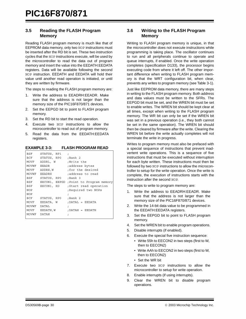
3.5 Reading the FLASH Program Memory
Reading FLASH program memory is much like that ofEEPROM data memory, only two NOP instructions mustbe inserted after the RD bit is set. These two instructioncycles that the NOP instructions execute, will be used bythe microcontroller to read the data out of programmemory and insert the value into the EEDATH:EEDATAregisters. Data will be available following the secondNOP instruction. EEDATH and EEDATA will hold theirvalue until another read operation is initiated, or untilthey are written by firmware.
The steps to reading the FLASH program memory are:
1. Write the address to EEADRH:EEADR. Makesure that the address is not larger than thememory size of the PIC16F870/871 devices.
2. Set the EEPGD bit to point to FLASH programmemory.
3. Set the RD bit to start the read operation.
4. Execute two NOP instructions to allow themicrocontroller to read out of program memory.
5. Read the data from the EEDATH:EEDATAregisters.
EXAMPLE 3-3: FLASH PROGRAM READ
3.6 Writing to the FLASH Program Memory
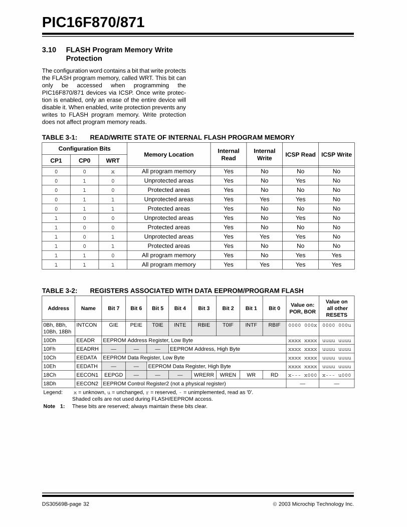
Writing to FLASH program memory is unique, in thatthe microcontroller does not execute instructions whileprogramming is taking place. The oscillator continuesto run and all peripherals continue to operate andqueue interrupts, if enabled. Once the write operationcompletes (specification D133), the processor beginsexecuting code from where it left off. The other impor-tant difference when writing to FLASH program mem-ory is that the WRT configuration bit, when clear,prevents any writes to program memory (see Table 3-1).
Just like EEPROM data memory, there are many stepsin writing to the FLASH program memory. Both addressand data values must be written to the SFRs. TheEEPGD bit must be set, and the WREN bit must be setto enable writes. The WREN bit should be kept clear atall times, except when writing to the FLASH programmemory. The WR bit can only be set if the WREN bitwas set in a previous operation (i.e., they both cannotbe set in the same operation). The WREN bit shouldthen be cleared by firmware after the write. Clearing theWREN bit before the write actually completes will notterminate the write in progress.
Writes to program memory must also be prefaced witha special sequence of instructions that prevent inad-vertent write operations. This is a sequence of fiveinstructions that must be executed without interruptionfor each byte written. These instructions must then befollowed by two NOP instructions to allow the microcon-troller to setup for the write operation. Once the write iscomplete, the execution of instructions starts with theinstruction after the second NOP.
The steps to write to program memory are:
1. Write the address to EEADRH:EEADR. Makesure that the address is not larger than thememory size of the PIC16F870/871 devices.
2. Write the 14-bit data value to be programmed inthe EEDATH:EEDATA registers.
3. Set the EEPGD bit to point to FLASH programmemory.
4. Set the WREN bit to enable program operations.5. Disable interrupts (if enabled).
6. Execute the special five instruction sequence:• Write 55h to EECON2 in two steps (first to W,
then to EECON2)• Write AAh to EECON2 in two steps (first to W,
then to EECON2)• Set the WR bit
7. Execute two NOP instructions to allow themicrocontroller to setup for write operation.
8. Enable interrupts (if using interrupts).
9. Clear the WREN bit to disable programoperations.
BSF STATUS, RP1 ;BCF STATUS, RP0 ;Bank 2MOVF ADDRL, W ;Write theMOVWF EEADR ;address bytesMOVF ADDRH,W ;for the desiredMOVWF EEADRH ;address to readBSF STATUS, RP0 ;Bank 3BSF EECON1, EEPGD ;Point to Program memoryBSF EECON1, RD ;Start read operationNOP ;Required two NOPsNOP ;BCF STATUS, RP0 ;Bank 2MOVF EEDATA, W ;DATAL = EEDATAMOVWF DATAL ;MOVF EEDATH,W ;DATAH = EEDATHMOVWF DATAH ;
DS30569B-page 30 2003 Microchip Technology Inc.
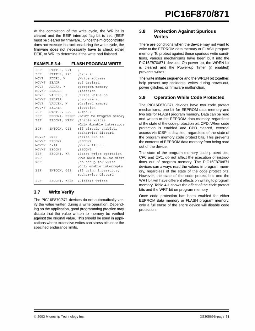
PIC16F870/871
At the completion of the write cycle, the WR bit iscleared and the EEIF interrupt flag bit is set. (EEIFmust be cleared by firmware.) Since the microcontrollerdoes not execute instructions during the write cycle, thefirmware does not necessarily have to check eitherEEIF, or WR, to determine if the write had finished.
EXAMPLE 3-4: FLASH PROGRAM WRITE
3.7 Write Verify
The PIC16F870/871 devices do not automatically ver-ify the value written during a write operation. Depend-ing on the application, good programming practice maydictate that the value written to memory be verifiedagainst the original value. This should be used in appli-cations where excessive writes can stress bits near thespecified endurance limits.
3.8 Protection Against Spurious Writes
There are conditions when the device may not want towrite to the EEPROM data memory or FLASH programmemory. To protect against these spurious write condi-tions, various mechanisms have been built into thePIC16F870/871 devices. On power-up, the WREN bitis cleared and the Power-up Timer (if enabled)prevents writes.
The write initiate sequence and the WREN bit together,help prevent any accidental writes during brown-out,power glitches, or firmware malfunction.
3.9 Operation While Code Protected
The PIC16F870/871 devices have two code protectmechanisms, one bit for EEPROM data memory andtwo bits for FLASH program memory. Data can be readand written to the EEPROM data memory, regardlessof the state of the code protection bit, CPD. When codeprotection is enabled and CPD cleared, externalaccess via ICSP is disabled, regardless of the state ofthe program memory code protect bits. This preventsthe contents of EEPROM data memory from being readout of the device.
The state of the program memory code protect bits,CP0 and CP1, do not affect the execution of instruc-tions out of program memory. The PIC16F870/871devices can always read the values in program mem-ory, regardless of the state of the code protect bits.However, the state of the code protect bits and theWRT bit will have different effects on writing to programmemory. Table 4-1 shows the effect of the code protectbits and the WRT bit on program memory.
Once code protection has been enabled for eitherEEPROM data memory or FLASH program memory,only a full erase of the entire device will disable codeprotection.
BSF STATUS, RP1 ;BCF STATUS, RP0 ;Bank 2MOVF ADDRL, W ;Write addressMOVWF EEADR ;of desiredMOVF ADDRH, W ;program memoryMOVWF EEADRH ;locationMOVF VALUEL, W ;Write value toMOVWF EEDATA ;program atMOVF VALUEH, W ;desired memoryMOVWF EEDATH ;locationBSF STATUS, RP0 ;Bank 3BSF EECON1, EEPGD ;Point to Program memoryBSF EECON1, WREN ;Enable writes ;Only disable interruptsBCF INTCON, GIE ;if already enabled, ;otherwise discardMOVLW 0x55 ;Write 55h toMOVWF EECON2 ;EECON2MOVLW 0xAA ;Write AAh toMOVWF EECON2 ;EECON2BSF EECON1, WR ;Start write operationNOP ;Two NOPs to allow microNOP ;to setup for write ;Only enable interruptsBSF INTCON, GIE ;if using interrupts, ;otherwise discard
BCF EECON1, WREN ;Disable writes
2003 Microchip Technology Inc. DS30569B-page 31
PIC16F870/871
3.10 FLASH Program Memory Write Protection
The configuration word contains a bit that write protectsthe FLASH program memory, called WRT. This bit canonly be accessed when programming thePIC16F870/871 devices via ICSP. Once write protec-tion is enabled, only an erase of the entire device willdisable it. When enabled, write protection prevents anywrites to FLASH program memory. Write protectiondoes not affect program memory reads.
TABLE 3-1: READ/WRITE STATE OF INTERNAL FLASH PROGRAM MEMORY
TABLE 3-2: REGISTERS ASSOCIATED WITH DATA EEPROM/PROGRAM FLASH
Configuration BitsMemory Location
Internal Read
Internal Write
ICSP Read ICSP WriteCP1 CP0 WRT
0 0 x All program memory Yes No No No
0 1 0 Unprotected areas Yes No Yes No
0 1 0 Protected areas Yes No No No
0 1 1 Unprotected areas Yes Yes Yes No
0 1 1 Protected areas Yes No No No
1 0 0 Unprotected areas Yes No Yes No
1 0 0 Protected areas Yes No No No
1 0 1 Unprotected areas Yes Yes Yes No
1 0 1 Protected areas Yes No No No
1 1 0 All program memory Yes No Yes Yes
1 1 1 All program memory Yes Yes Yes Yes
Address Name Bit 7 Bit 6 Bit 5 Bit 4 Bit 3 Bit 2 Bit 1 Bit 0Value on:POR, BOR
Value on all other RESETS
0Bh, 8Bh,10Bh, 18Bh
INTCON GIE PEIE T0IE INTE RBIE T0IF INTF RBIF 0000 000x 0000 000u
10Dh EEADR EEPROM Address Register, Low Byte xxxx xxxx uuuu uuuu
10Fh EEADRH — — — EEPROM Address, High Byte xxxx xxxx uuuu uuuu
10Ch EEDATA EEPROM Data Register, Low Byte xxxx xxxx uuuu uuuu
10Eh EEDATH — — EEPROM Data Register, High Byte xxxx xxxx uuuu uuuu
18Ch EECON1 EEPGD — — — WRERR WREN WR RD x--- x000 x--- u000
18Dh EECON2 EEPROM Control Register2 (not a physical register) — —
Legend: x = unknown, u = unchanged, r = reserved, - = unimplemented, read as '0'. Shaded cells are not used during FLASH/EEPROM access.
Note 1: These bits are reserved; always maintain these bits clear.
DS30569B-page 32 2003 Microchip Technology Inc.
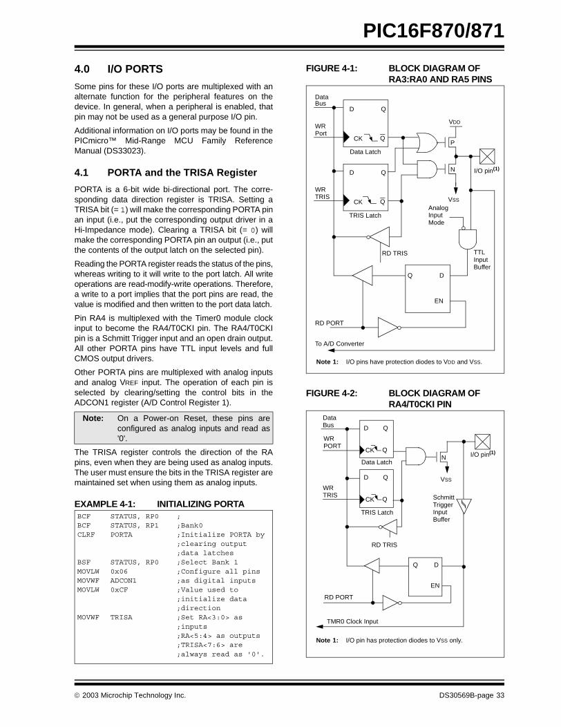
PIC16F870/871
4.0 I/O PORTS
Some pins for these I/O ports are multiplexed with analternate function for the peripheral features on thedevice. In general, when a peripheral is enabled, thatpin may not be used as a general purpose I/O pin.
Additional information on I/O ports may be found in thePICmicro™ Mid-Range MCU Family ReferenceManual (DS33023).
4.1 PORTA and the TRISA Register
PORTA is a 6-bit wide bi-directional port. The corre-sponding data direction register is TRISA. Setting aTRISA bit (= 1) will make the corresponding PORTA pinan input (i.e., put the corresponding output driver in aHi-Impedance mode). Clearing a TRISA bit (= 0) willmake the corresponding PORTA pin an output (i.e., putthe contents of the output latch on the selected pin).
Reading the PORTA register reads the status of the pins,whereas writing to it will write to the port latch. All writeoperations are read-modify-write operations. Therefore,a write to a port implies that the port pins are read, thevalue is modified and then written to the port data latch.
Pin RA4 is multiplexed with the Timer0 module clockinput to become the RA4/T0CKI pin. The RA4/T0CKIpin is a Schmitt Trigger input and an open drain output.All other PORTA pins have TTL input levels and fullCMOS output drivers.
Other PORTA pins are multiplexed with analog inputsand analog VREF input. The operation of each pin isselected by clearing/setting the control bits in theADCON1 register (A/D Control Register 1).
The TRISA register controls the direction of the RApins, even when they are being used as analog inputs.The user must ensure the bits in the TRISA register aremaintained set when using them as analog inputs.
EXAMPLE 4-1: INITIALIZING PORTA
FIGURE 4-1: BLOCK DIAGRAM OF RA3:RA0 AND RA5 PINS
FIGURE 4-2: BLOCK DIAGRAM OF RA4/T0CKI PIN
Note: On a Power-on Reset, these pins areconfigured as analog inputs and read as'0'.
BCF STATUS, RP0 ;BCF STATUS, RP1 ;Bank0CLRF PORTA ;Initialize PORTA by
;clearing output;data latches
BSF STATUS, RP0 ;Select Bank 1MOVLW 0x06 ;Configure all pinsMOVWF ADCON1 ;as digital inputsMOVLW 0xCF ;Value used to
;initialize data ;direction
MOVWF TRISA ;Set RA<3:0> as;inputs;RA<5:4> as outputs;TRISA<7:6> are;always read as '0'.
DataBus
QD
QCK
QD
QCK
Q D
EN
P
N
WRPort
WRTRIS
Data Latch
TRIS Latch
RD TRIS
RD PORT
VSS
VDD
I/O pin(1)
Note 1: I/O pins have protection diodes to VDD and VSS.
AnalogInputMode
TTLInputBuffer
To A/D Converter
DataBus
WRPORT
WRTRIS
RD PORT
Data Latch
TRIS Latch
RD TRIS
SchmittTriggerInputBuffer
N
VSS
I/O pin(1)
TMR0 Clock Input
QD
QCK
QD
QCK
EN
Q D
EN
Note 1: I/O pin has protection diodes to VSS only.
2003 Microchip Technology Inc. DS30569B-page 33
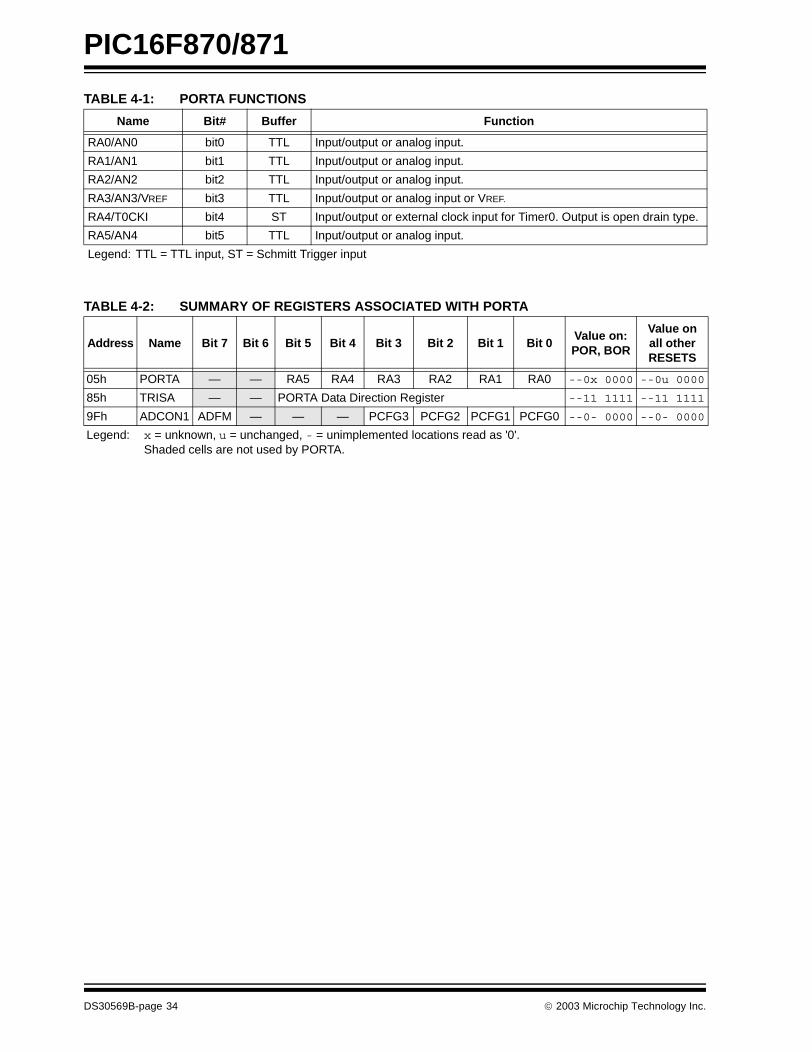
PIC16F870/871
TABLE 4-1: PORTA FUNCTIONS
TABLE 4-2: SUMMARY OF REGISTERS ASSOCIATED WITH PORTA
Name Bit# Buffer Function
RA0/AN0 bit0 TTL Input/output or analog input.
RA1/AN1 bit1 TTL Input/output or analog input.
RA2/AN2 bit2 TTL Input/output or analog input.
RA3/AN3/VREF bit3 TTL Input/output or analog input or VREF.
RA4/T0CKI bit4 ST Input/output or external clock input for Timer0. Output is open drain type.
RA5/AN4 bit5 TTL Input/output or analog input.
Legend: TTL = TTL input, ST = Schmitt Trigger input
Address Name Bit 7 Bit 6 Bit 5 Bit 4 Bit 3 Bit 2 Bit 1 Bit 0Value on: POR, BOR
Value on all other RESETS
05h PORTA — — RA5 RA4 RA3 RA2 RA1 RA0 --0x 0000 --0u 0000
85h TRISA — — PORTA Data Direction Register --11 1111 --11 1111
9Fh ADCON1 ADFM — — — PCFG3 PCFG2 PCFG1 PCFG0 --0- 0000 --0- 0000
Legend: x = unknown, u = unchanged, - = unimplemented locations read as '0'. Shaded cells are not used by PORTA.
DS30569B-page 34 2003 Microchip Technology Inc.
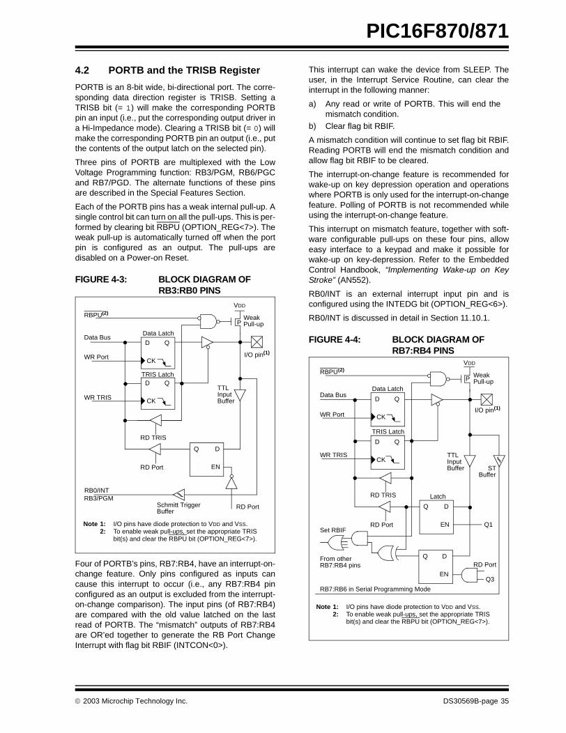
PIC16F870/871
4.2 PORTB and the TRISB Register
PORTB is an 8-bit wide, bi-directional port. The corre-sponding data direction register is TRISB. Setting aTRISB bit (= 1) will make the corresponding PORTBpin an input (i.e., put the corresponding output driver ina Hi-Impedance mode). Clearing a TRISB bit (= 0) willmake the corresponding PORTB pin an output (i.e., putthe contents of the output latch on the selected pin).
Three pins of PORTB are multiplexed with the LowVoltage Programming function: RB3/PGM, RB6/PGCand RB7/PGD. The alternate functions of these pinsare described in the Special Features Section.
Each of the PORTB pins has a weak internal pull-up. Asingle control bit can turn on all the pull-ups. This is per-formed by clearing bit RBPU (OPTION_REG<7>). Theweak pull-up is automatically turned off when the portpin is configured as an output. The pull-ups aredisabled on a Power-on Reset.
FIGURE 4-3: BLOCK DIAGRAM OF RB3:RB0 PINS
Four of PORTB’s pins, RB7:RB4, have an interrupt-on-change feature. Only pins configured as inputs cancause this interrupt to occur (i.e., any RB7:RB4 pinconfigured as an output is excluded from the interrupt-on-change comparison). The input pins (of RB7:RB4)are compared with the old value latched on the lastread of PORTB. The “mismatch” outputs of RB7:RB4are OR’ed together to generate the RB Port ChangeInterrupt with flag bit RBIF (INTCON<0>).
This interrupt can wake the device from SLEEP. Theuser, in the Interrupt Service Routine, can clear theinterrupt in the following manner:
a) Any read or write of PORTB. This will end themismatch condition.
b) Clear flag bit RBIF.
A mismatch condition will continue to set flag bit RBIF.Reading PORTB will end the mismatch condition andallow flag bit RBIF to be cleared.
The interrupt-on-change feature is recommended forwake-up on key depression operation and operationswhere PORTB is only used for the interrupt-on-changefeature. Polling of PORTB is not recommended whileusing the interrupt-on-change feature.
This interrupt on mismatch feature, together with soft-ware configurable pull-ups on these four pins, alloweasy interface to a keypad and make it possible forwake-up on key-depression. Refer to the EmbeddedControl Handbook, “Implementing Wake-up on KeyStroke” (AN552).
RB0/INT is an external interrupt input pin and isconfigured using the INTEDG bit (OPTION_REG<6>).
RB0/INT is discussed in detail in Section 11.10.1.
FIGURE 4-4: BLOCK DIAGRAM OFRB7:RB4 PINS
Data Latch
RBPU(2)
P
VDD
QD
CK
QD
CK
Q D
EN
Data Bus
WR Port
WR TRIS
RD TRIS
RD Port
WeakPull-up
RD Port
RB0/INT
I/O pin(1)
TTLInputBuffer
Schmitt TriggerBuffer
TRIS Latch
Note 1: I/O pins have diode protection to VDD and VSS.2: To enable weak pull-ups, set the appropriate TRIS
bit(s) and clear the RBPU bit (OPTION_REG<7>).
RB3/PGM
Data Latch
From other
RBPU(2)
P
VDD
I/O pin(1)
QD
CK
QD
CK
Q D
EN
Q D
EN
Data Bus
WR Port
WR TRIS
Set RBIF
TRIS Latch
RD TRIS
RD Port
RB7:RB4 pins
WeakPull-up
RD Port
Latch
TTLInputBuffer ST
Buffer
RB7:RB6 in Serial Programming Mode
Q3
Q1
Note 1: I/O pins have diode protection to VDD and VSS.2: To enable weak pull-ups, set the appropriate TRIS
bit(s) and clear the RBPU bit (OPTION_REG<7>).
2003 Microchip Technology Inc. DS30569B-page 35
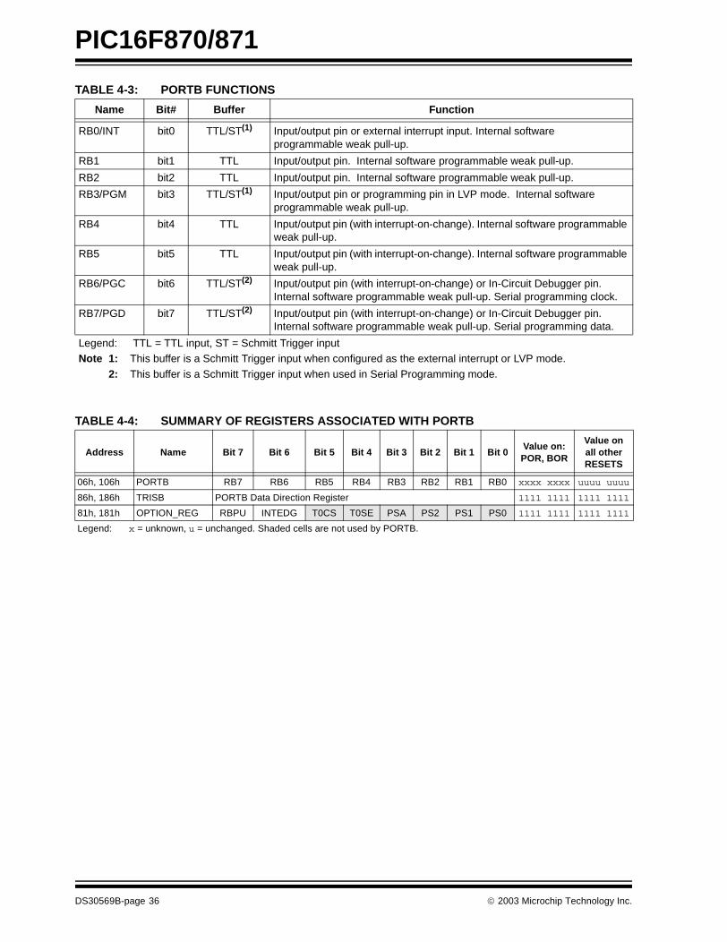
PIC16F870/871
TABLE 4-3: PORTB FUNCTIONS
TABLE 4-4: SUMMARY OF REGISTERS ASSOCIATED WITH PORTB
Name Bit# Buffer Function
RB0/INT bit0 TTL/ST(1) Input/output pin or external interrupt input. Internal software programmable weak pull-up.
RB1 bit1 TTL Input/output pin. Internal software programmable weak pull-up.
RB2 bit2 TTL Input/output pin. Internal software programmable weak pull-up.
RB3/PGM bit3 TTL/ST(1) Input/output pin or programming pin in LVP mode. Internal software programmable weak pull-up.
RB4 bit4 TTL Input/output pin (with interrupt-on-change). Internal software programmable weak pull-up.
RB5 bit5 TTL Input/output pin (with interrupt-on-change). Internal software programmable weak pull-up.
RB6/PGC bit6 TTL/ST(2) Input/output pin (with interrupt-on-change) or In-Circuit Debugger pin. Internal software programmable weak pull-up. Serial programming clock.
RB7/PGD bit7 TTL/ST(2) Input/output pin (with interrupt-on-change) or In-Circuit Debugger pin. Internal software programmable weak pull-up. Serial programming data.
Legend: TTL = TTL input, ST = Schmitt Trigger inputNote 1: This buffer is a Schmitt Trigger input when configured as the external interrupt or LVP mode.
2: This buffer is a Schmitt Trigger input when used in Serial Programming mode.
Address Name Bit 7 Bit 6 Bit 5 Bit 4 Bit 3 Bit 2 Bit 1 Bit 0Value on: POR, BOR
Value on all other RESETS
06h, 106h PORTB RB7 RB6 RB5 RB4 RB3 RB2 RB1 RB0 xxxx xxxx uuuu uuuu
86h, 186h TRISB PORTB Data Direction Register 1111 1111 1111 1111
81h, 181h OPTION_REG RBPU INTEDG T0CS T0SE PSA PS2 PS1 PS0 1111 1111 1111 1111
Legend: x = unknown, u = unchanged. Shaded cells are not used by PORTB.
DS30569B-page 36 2003 Microchip Technology Inc.
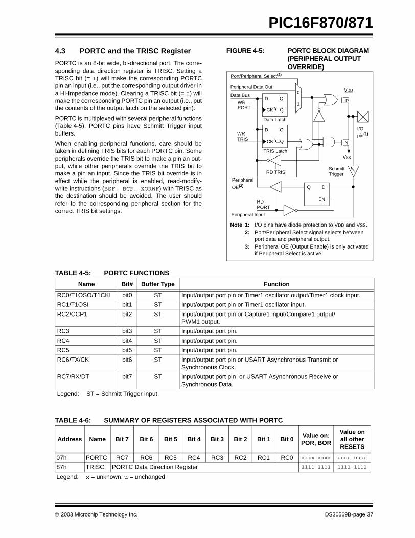
PIC16F870/871
4.3 PORTC and the TRISC Register
PORTC is an 8-bit wide, bi-directional port. The corre-sponding data direction register is TRISC. Setting aTRISC bit (= 1) will make the corresponding PORTCpin an input (i.e., put the corresponding output driver ina Hi-Impedance mode). Clearing a TRISC bit (= 0) willmake the corresponding PORTC pin an output (i.e., putthe contents of the output latch on the selected pin).
PORTC is multiplexed with several peripheral functions(Table 4-5). PORTC pins have Schmitt Trigger inputbuffers.
When enabling peripheral functions, care should betaken in defining TRIS bits for each PORTC pin. Someperipherals override the TRIS bit to make a pin an out-put, while other peripherals override the TRIS bit tomake a pin an input. Since the TRIS bit override is ineffect while the peripheral is enabled, read-modify-write instructions (BSF, BCF, XORWF) with TRISC asthe destination should be avoided. The user shouldrefer to the corresponding peripheral section for thecorrect TRIS bit settings.
FIGURE 4-5: PORTC BLOCK DIAGRAM (PERIPHERAL OUTPUT OVERRIDE)
TABLE 4-5: PORTC FUNCTIONS
TABLE 4-6: SUMMARY OF REGISTERS ASSOCIATED WITH PORTC
Port/Peripheral Select(2)
Data Bus
WRPORT
WRTRIS
RD
Data Latch
TRIS Latch
RD TRISSchmittTrigger
QD
QCK
Q D
EN
Peripheral Data Out0
1
QD
QCK
P
N
VDD
Vss
PORT
Peripheral
OE(3)
Peripheral Input
I/Opin(1)
Note 1: I/O pins have diode protection to VDD and VSS.2: Port/Peripheral Select signal selects between
port data and peripheral output.3: Peripheral OE (Output Enable) is only activated
if Peripheral Select is active.
Name Bit# Buffer Type Function
RC0/T1OSO/T1CKI bit0 ST Input/output port pin or Timer1 oscillator output/Timer1 clock input.
RC1/T1OSI bit1 ST Input/output port pin or Timer1 oscillator input.
RC2/CCP1 bit2 ST Input/output port pin or Capture1 input/Compare1 output/PWM1 output.
RC3 bit3 ST Input/output port pin.
RC4 bit4 ST Input/output port pin.
RC5 bit5 ST Input/output port pin.
RC6/TX/CK bit6 ST Input/output port pin or USART Asynchronous Transmit or Synchronous Clock.
RC7/RX/DT bit7 ST Input/output port pin or USART Asynchronous Receive or Synchronous Data.
Legend: ST = Schmitt Trigger input
Address Name Bit 7 Bit 6 Bit 5 Bit 4 Bit 3 Bit 2 Bit 1 Bit 0Value on: POR, BOR
Value on all other RESETS
07h PORTC RC7 RC6 RC5 RC4 RC3 RC2 RC1 RC0 xxxx xxxx uuuu uuuu
87h TRISC PORTC Data Direction Register 1111 1111 1111 1111
Legend: x = unknown, u = unchanged
2003 Microchip Technology Inc. DS30569B-page 37
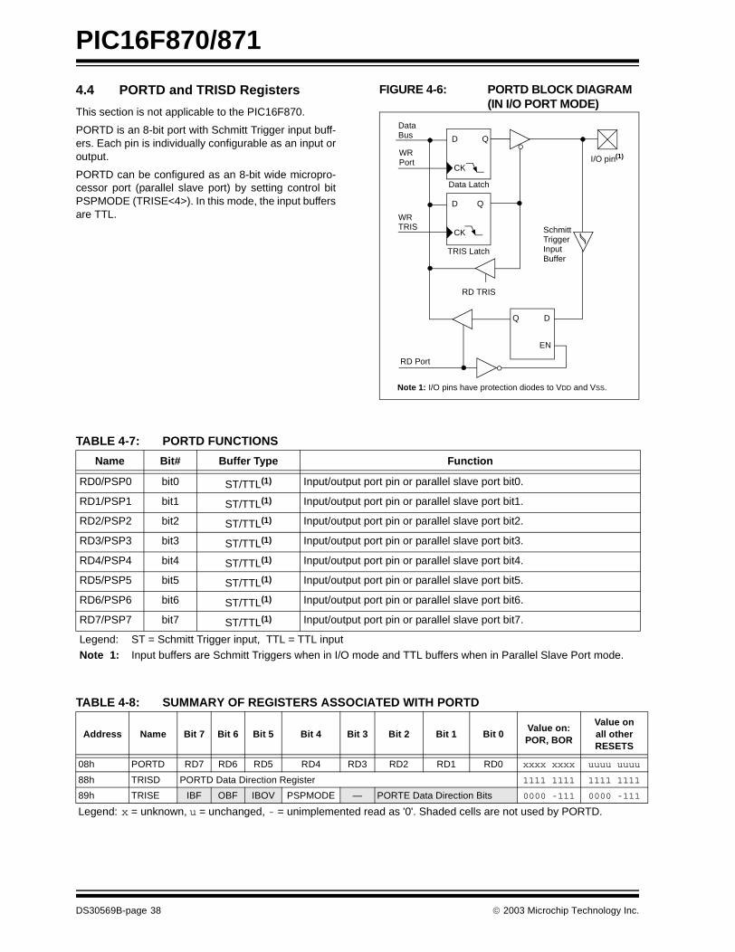
PIC16F870/871
4.4 PORTD and TRISD Registers
This section is not applicable to the PIC16F870.
PORTD is an 8-bit port with Schmitt Trigger input buff-ers. Each pin is individually configurable as an input oroutput.
PORTD can be configured as an 8-bit wide micropro-cessor port (parallel slave port) by setting control bitPSPMODE (TRISE<4>). In this mode, the input buffersare TTL.
FIGURE 4-6: PORTD BLOCK DIAGRAM (IN I/O PORT MODE)
TABLE 4-7: PORTD FUNCTIONS
TABLE 4-8: SUMMARY OF REGISTERS ASSOCIATED WITH PORTD
DataBus
WRPort
WRTRIS
RD Port
Data Latch
TRIS Latch
RD TRIS
SchmittTriggerInputBuffer
I/O pin(1)
Note 1: I/O pins have protection diodes to VDD and VSS.
QD
CK
QD
CK
EN
Q D
EN
Name Bit# Buffer Type Function
RD0/PSP0 bit0 ST/TTL(1) Input/output port pin or parallel slave port bit0.
RD1/PSP1 bit1 ST/TTL(1) Input/output port pin or parallel slave port bit1.
RD2/PSP2 bit2 ST/TTL(1) Input/output port pin or parallel slave port bit2.
RD3/PSP3 bit3 ST/TTL(1) Input/output port pin or parallel slave port bit3.
RD4/PSP4 bit4 ST/TTL(1) Input/output port pin or parallel slave port bit4.
RD5/PSP5 bit5 ST/TTL(1) Input/output port pin or parallel slave port bit5.
RD6/PSP6 bit6 ST/TTL(1) Input/output port pin or parallel slave port bit6.
RD7/PSP7 bit7 ST/TTL(1) Input/output port pin or parallel slave port bit7.
Legend: ST = Schmitt Trigger input, TTL = TTL input
Note 1: Input buffers are Schmitt Triggers when in I/O mode and TTL buffers when in Parallel Slave Port mode.
Address Name Bit 7 Bit 6 Bit 5 Bit 4 Bit 3 Bit 2 Bit 1 Bit 0Value on: POR, BOR
Value on all other RESETS
08h PORTD RD7 RD6 RD5 RD4 RD3 RD2 RD1 RD0 xxxx xxxx uuuu uuuu
88h TRISD PORTD Data Direction Register 1111 1111 1111 1111
89h TRISE IBF OBF IBOV PSPMODE — PORTE Data Direction Bits 0000 -111 0000 -111
Legend: x = unknown, u = unchanged, - = unimplemented read as '0'. Shaded cells are not used by PORTD.
DS30569B-page 38 2003 Microchip Technology Inc.
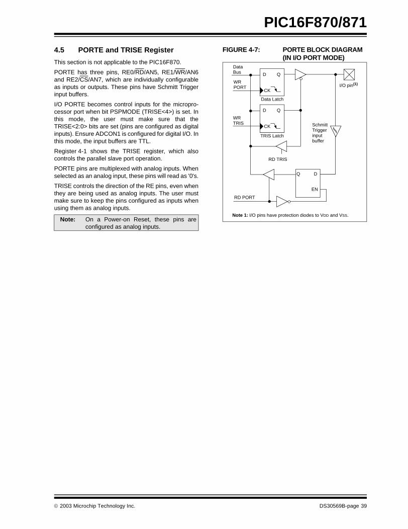
PIC16F870/871
4.5 PORTE and TRISE Register
This section is not applicable to the PIC16F870.
PORTE has three pins, RE0/RD/AN5, RE1/WR/AN6and RE2/CS/AN7, which are individually configurableas inputs or outputs. These pins have Schmitt Triggerinput buffers.
I/O PORTE becomes control inputs for the micropro-cessor port when bit PSPMODE (TRISE<4>) is set. Inthis mode, the user must make sure that theTRISE<2:0> bits are set (pins are configured as digitalinputs). Ensure ADCON1 is configured for digital I/O. Inthis mode, the input buffers are TTL.
Register 4-1 shows the TRISE register, which alsocontrols the parallel slave port operation.
PORTE pins are multiplexed with analog inputs. Whenselected as an analog input, these pins will read as '0's.
TRISE controls the direction of the RE pins, even whenthey are being used as analog inputs. The user mustmake sure to keep the pins configured as inputs whenusing them as analog inputs.
FIGURE 4-7: PORTE BLOCK DIAGRAM (IN I/O PORT MODE)
Note: On a Power-on Reset, these pins areconfigured as analog inputs.
DataBus
WRPORT
WRTRIS
RD PORT
Data Latch
TRIS Latch
RD TRIS
SchmittTriggerinputbuffer
QD
CK
QD
CK
Q D
EN
I/O pin(1)
Note 1: I/O pins have protection diodes to VDD and VSS.
2003 Microchip Technology Inc. DS30569B-page 39
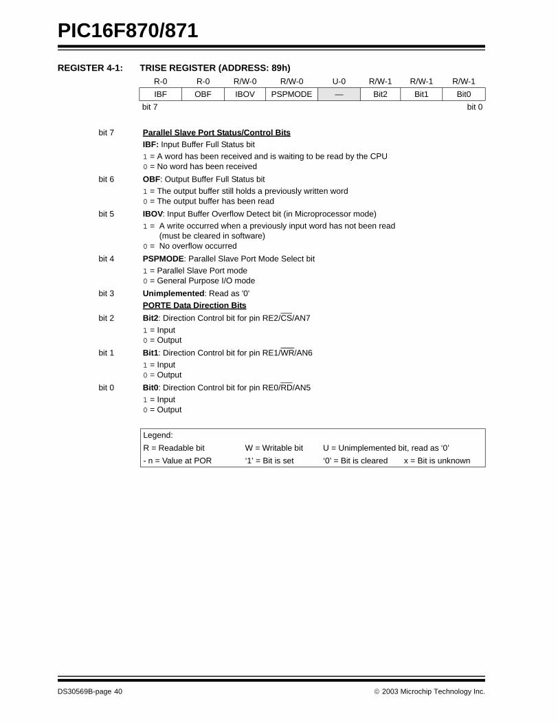
PIC16F870/871
REGISTER 4-1: TRISE REGISTER (ADDRESS: 89h) R-0 R-0 R/W-0 R/W-0 U-0 R/W-1 R/W-1 R/W-1
IBF OBF IBOV PSPMODE — Bit2 Bit1 Bit0
bit 7 bit 0
bit 7 Parallel Slave Port Status/Control BitsIBF: Input Buffer Full Status bit1 = A word has been received and is waiting to be read by the CPU0 = No word has been received
bit 6 OBF: Output Buffer Full Status bit1 = The output buffer still holds a previously written word0 = The output buffer has been read
bit 5 IBOV: Input Buffer Overflow Detect bit (in Microprocessor mode)
1 = A write occurred when a previously input word has not been read (must be cleared in software)
0 = No overflow occurred
bit 4 PSPMODE: Parallel Slave Port Mode Select bit1 = Parallel Slave Port mode0 = General Purpose I/O mode
bit 3 Unimplemented: Read as '0'
PORTE Data Direction Bits
bit 2 Bit2: Direction Control bit for pin RE2/CS/AN7
1 = Input0 = Output
bit 1 Bit1: Direction Control bit for pin RE1/WR/AN61 = Input0 = Output
bit 0 Bit0: Direction Control bit for pin RE0/RD/AN51 = Input0 = Output
Legend:
R = Readable bit W = Writable bit U = Unimplemented bit, read as ‘0’
- n = Value at POR ‘1’ = Bit is set ‘0’ = Bit is cleared x = Bit is unknown
DS30569B-page 40 2003 Microchip Technology Inc.
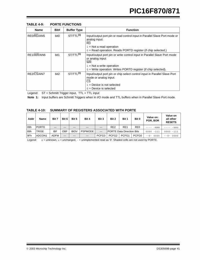
PIC16F870/871
TABLE 4-9: PORTE FUNCTIONS
TABLE 4-10: SUMMARY OF REGISTERS ASSOCIATED WITH PORTE
Name Bit# Buffer Type Function
RE0/RD/AN5 bit0 ST/TTL(1) Input/output port pin or read control input in Parallel Slave Port mode or analog input:RD1 = Not a read operation0 = Read operation. Reads PORTD register (if chip selected.)
RE1/WR/AN6 bit1 ST/TTL(1) Input/output port pin or write control input in Parallel Slave Port mode or analog input:WR1 = Not a write operation0 = Write operation. Writes PORTD register (if chip selected).
RE2/CS/AN7 bit2 ST/TTL(1) Input/output port pin or chip select control input in Parallel Slave Port mode or analog input:CS1 = Device is not selected0 = Device is selected
Legend: ST = Schmitt Trigger input, TTL = TTL input Note 1: Input buffers are Schmitt Triggers when in I/O mode and TTL buffers when in Parallel Slave Port mode.
Addr Name Bit 7 Bit 6 Bit 5 Bit 4 Bit 3 Bit 2 Bit 1 Bit 0Value on: POR, BOR
Value on all other RESETS
09h PORTE — — — — — RE2 RE1 RE0 ---- -xxx ---- -uuu
89h TRISE IBF OBF IBOV PSPMODE — PORTE Data Direction Bits 0000 -111 0000 -111
9Fh ADCON1 ADFM — — — PCFG3 PCFG2 PCFG1 PCFG0 --0- 0000 --0- 0000
Legend: x = unknown, u = unchanged, - = unimplemented read as '0'. Shaded cells are not used by PORTE.
2003 Microchip Technology Inc. DS30569B-page 41
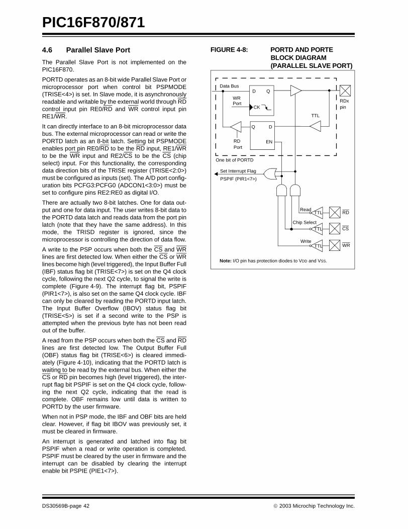
PIC16F870/871
4.6 Parallel Slave Port
The Parallel Slave Port is not implemented on thePIC16F870.
PORTD operates as an 8-bit wide Parallel Slave Port ormicroprocessor port when control bit PSPMODE(TRISE<4>) is set. In Slave mode, it is asynchronouslyreadable and writable by the external world through RDcontrol input pin RE0/RD and WR control input pinRE1/WR.
It can directly interface to an 8-bit microprocessor databus. The external microprocessor can read or write thePORTD latch as an 8-bit latch. Setting bit PSPMODEenables port pin RE0/RD to be the RD input, RE1/WRto be the WR input and RE2/CS to be the CS (chipselect) input. For this functionality, the correspondingdata direction bits of the TRISE register (TRISE<2:0>)must be configured as inputs (set). The A/D port config-uration bits PCFG3:PCFG0 (ADCON1<3:0>) must beset to configure pins RE2:RE0 as digital I/O.
There are actually two 8-bit latches. One for data out-put and one for data input. The user writes 8-bit data tothe PORTD data latch and reads data from the port pinlatch (note that they have the same address). In thismode, the TRISD register is ignored, since themicroprocessor is controlling the direction of data flow.
A write to the PSP occurs when both the CS and WRlines are first detected low. When either the CS or WRlines become high (level triggered), the Input Buffer Full(IBF) status flag bit (TRISE<7>) is set on the Q4 clockcycle, following the next Q2 cycle, to signal the write iscomplete (Figure 4-9). The interrupt flag bit, PSPIF(PIR1<7>), is also set on the same Q4 clock cycle. IBFcan only be cleared by reading the PORTD input latch.The Input Buffer Overflow (IBOV) status flag bit(TRISE<5>) is set if a second write to the PSP isattempted when the previous byte has not been readout of the buffer.
A read from the PSP occurs when both the CS and RDlines are first detected low. The Output Buffer Full(OBF) status flag bit (TRISE<6>) is cleared immedi-ately (Figure 4-10), indicating that the PORTD latch iswaiting to be read by the external bus. When either theCS or RD pin becomes high (level triggered), the inter-rupt flag bit PSPIF is set on the Q4 clock cycle, follow-ing the next Q2 cycle, indicating that the read iscomplete. OBF remains low until data is written toPORTD by the user firmware.
When not in PSP mode, the IBF and OBF bits are heldclear. However, if flag bit IBOV was previously set, itmust be cleared in firmware.
An interrupt is generated and latched into flag bitPSPIF when a read or write operation is completed.PSPIF must be cleared by the user in firmware and theinterrupt can be disabled by clearing the interruptenable bit PSPIE (PIE1<7>).
FIGURE 4-8: PORTD AND PORTE BLOCK DIAGRAM (PARALLEL SLAVE PORT)
Data Bus
WRPort
RD
RDx
QD
CK
EN
Q D
ENPort
pin
One bit of PORTD
Set Interrupt Flag
PSPIF (PIR1<7>)
Read
Chip Select
Write
RD
CS
WR
Note: I/O pin has protection diodes to VDD and VSS.
TTL
TTL
TTL
TTL
DS30569B-page 42 2003 Microchip Technology Inc.
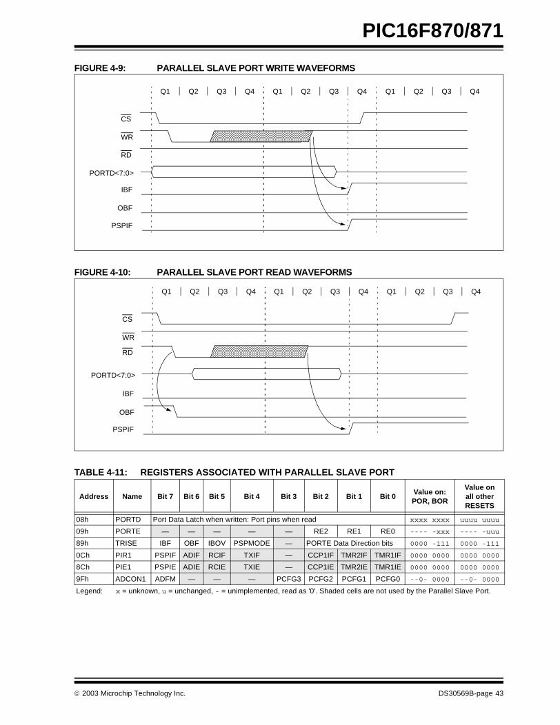
PIC16F870/871
FIGURE 4-9: PARALLEL SLAVE PORT WRITE WAVEFORMS
FIGURE 4-10: PARALLEL SLAVE PORT READ WAVEFORMS
TABLE 4-11: REGISTERS ASSOCIATED WITH PARALLEL SLAVE PORT
Address Name Bit 7 Bit 6 Bit 5 Bit 4 Bit 3 Bit 2 Bit 1 Bit 0Value on: POR, BOR
Value on all other RESETS
08h PORTD Port Data Latch when written: Port pins when read xxxx xxxx uuuu uuuu
09h PORTE — — — — — RE2 RE1 RE0 ---- -xxx ---- -uuu
89h TRISE IBF OBF IBOV PSPMODE — PORTE Data Direction bits 0000 -111 0000 -111
0Ch PIR1 PSPIF ADIF RCIF TXIF — CCP1IF TMR2IF TMR1IF 0000 0000 0000 0000
8Ch PIE1 PSPIE ADIE RCIE TXIE — CCP1IE TMR2IE TMR1IE 0000 0000 0000 0000
9Fh ADCON1 ADFM — — — PCFG3 PCFG2 PCFG1 PCFG0 --0- 0000 --0- 0000
Legend: x = unknown, u = unchanged, - = unimplemented, read as '0'. Shaded cells are not used by the Parallel Slave Port.
Q1 Q2 Q3 Q4
CS
Q1 Q2 Q3 Q4 Q1 Q2 Q3 Q4
WR
RD
IBF
OBF
PSPIF
PORTD<7:0>
Q1 Q2 Q3 Q4
CS
Q1 Q2 Q3 Q4 Q1 Q2 Q3 Q4
WR
IBF
PSPIF
RD
OBF
PORTD<7:0>
2003 Microchip Technology Inc. DS30569B-page 43
PIC16F870/871
NOTES:
DS30569B-page 44 2003 Microchip Technology Inc.
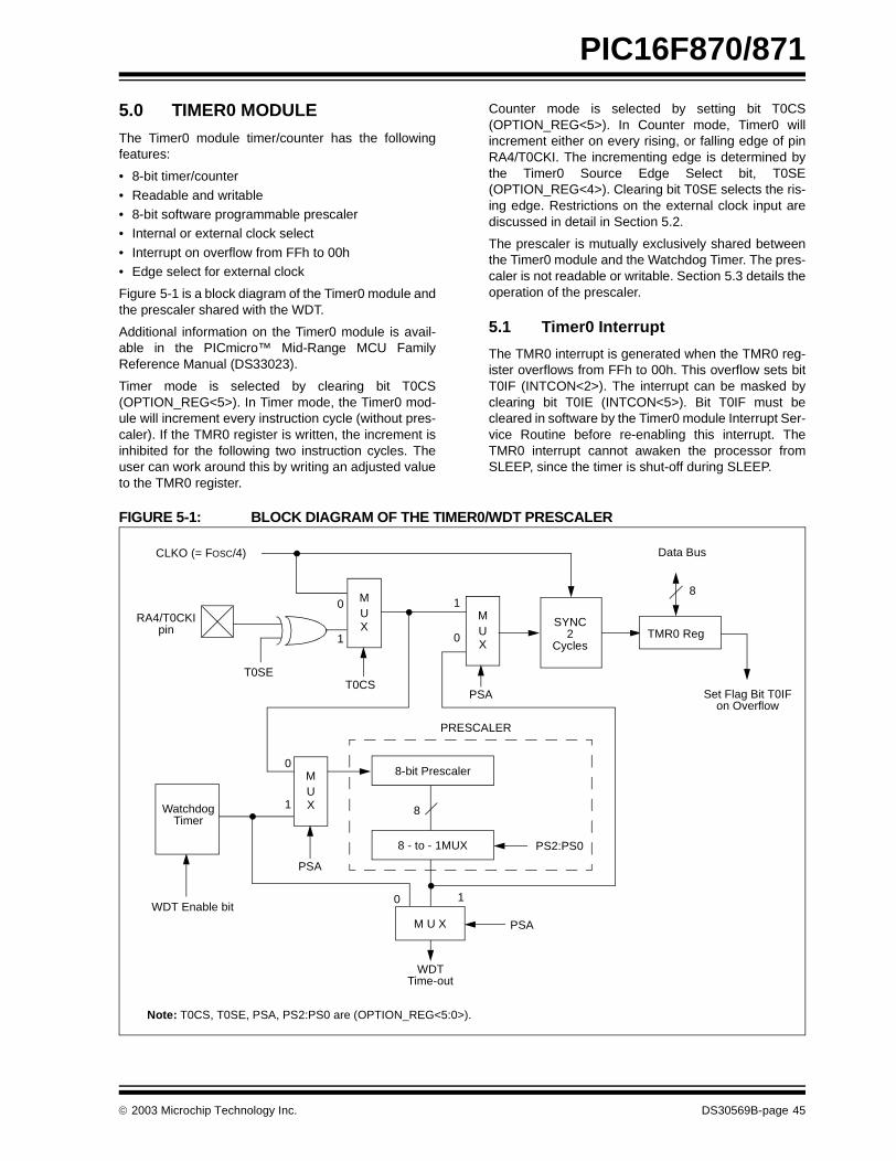
PIC16F870/871
5.0 TIMER0 MODULE
The Timer0 module timer/counter has the followingfeatures:
• 8-bit timer/counter
• Readable and writable• 8-bit software programmable prescaler• Internal or external clock select
• Interrupt on overflow from FFh to 00h• Edge select for external clock
Figure 5-1 is a block diagram of the Timer0 module andthe prescaler shared with the WDT.
Additional information on the Timer0 module is avail-able in the PICmicro™ Mid-Range MCU FamilyReference Manual (DS33023).
Timer mode is selected by clearing bit T0CS(OPTION_REG<5>). In Timer mode, the Timer0 mod-ule will increment every instruction cycle (without pres-caler). If the TMR0 register is written, the increment isinhibited for the following two instruction cycles. Theuser can work around this by writing an adjusted valueto the TMR0 register.
Counter mode is selected by setting bit T0CS(OPTION_REG<5>). In Counter mode, Timer0 willincrement either on every rising, or falling edge of pinRA4/T0CKI. The incrementing edge is determined bythe Timer0 Source Edge Select bit, T0SE(OPTION_REG<4>). Clearing bit T0SE selects the ris-ing edge. Restrictions on the external clock input arediscussed in detail in Section 5.2.
The prescaler is mutually exclusively shared betweenthe Timer0 module and the Watchdog Timer. The pres-caler is not readable or writable. Section 5.3 details theoperation of the prescaler.
5.1 Timer0 Interrupt
The TMR0 interrupt is generated when the TMR0 reg-ister overflows from FFh to 00h. This overflow sets bitT0IF (INTCON<2>). The interrupt can be masked byclearing bit T0IE (INTCON<5>). Bit T0IF must becleared in software by the Timer0 module Interrupt Ser-vice Routine before re-enabling this interrupt. TheTMR0 interrupt cannot awaken the processor fromSLEEP, since the timer is shut-off during SLEEP.
FIGURE 5-1: BLOCK DIAGRAM OF THE TIMER0/WDT PRESCALER
RA4/T0CKI
T0SE
pin
MUX
CLKO (= FOSC/4)
SYNC2
CyclesTMR0 Reg
8-bit Prescaler
8 - to - 1MUX
MUX
M U X
WatchdogTimer
PSA
0 1
0
1
WDTTime-out
PS2:PS0
8
Note: T0CS, T0SE, PSA, PS2:PS0 are (OPTION_REG<5:0>).
PSA
WDT Enable bit
MUX
0
1 0
1
Data Bus
Set Flag Bit T0IFon Overflow
8
PSAT0CS
PRESCALER
2003 Microchip Technology Inc. DS30569B-page 45
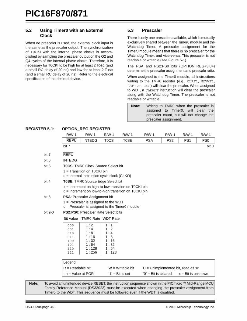
PIC16F870/871
5.2 Using Timer0 with an External Clock
When no prescaler is used, the external clock input isthe same as the prescaler output. The synchronizationof T0CKI with the internal phase clocks is accom-plished by sampling the prescaler output on the Q2 andQ4 cycles of the internal phase clocks. Therefore, it isnecessary for T0CKI to be high for at least 2 TOSC (anda small RC delay of 20 ns) and low for at least 2 TOSC
(and a small RC delay of 20 ns). Refer to the electricalspecification of the desired device.
5.3 Prescaler
There is only one prescaler available, which is mutuallyexclusively shared between the Timer0 module and theWatchdog Timer. A prescaler assignment for theTimer0 module means that there is no prescaler for theWatchdog Timer, and vice-versa. This prescaler is notreadable or writable (see Figure 5-1).
The PSA and PS2:PS0 bits (OPTION_REG<3:0>)determine the prescaler assignment and prescale ratio.
When assigned to the Timer0 module, all instructionswriting to the TMR0 register (e.g., CLRF1, MOVWF1,BSF1,x....etc.) will clear the prescaler. When assignedto WDT, a CLRWDT instruction will clear the prescaleralong with the Watchdog Timer. The prescaler is notreadable or writable.
REGISTER 5-1: OPTION_REG REGISTER
Note: Writing to TMR0 when the prescaler isassigned to Timer0, will clear theprescaler count, but will not change theprescaler assignment.
R/W-1 R/W-1 R/W-1 R/W-1 R/W-1 R/W-1 R/W-1 R/W-1
RBPU INTEDG T0CS T0SE PSA PS2 PS1 PS0
bit 7 bit 0
bit 7 RBPU
bit 6 INTEDG
bit 5 T0CS: TMR0 Clock Source Select bit1 = Transition on T0CKI pin0 = Internal instruction cycle clock (CLKO)
bit 4 T0SE: TMR0 Source Edge Select bit
1 = Increment on high-to-low transition on T0CKI pin0 = Increment on low-to-high transition on T0CKI pin
bit 3 PSA: Prescaler Assignment bit1 = Prescaler is assigned to the WDT 0 = Prescaler is assigned to the Timer0 module
bit 2-0 PS2:PS0: Prescaler Rate Select bits
Legend:
R = Readable bit W = Writable bit U = Unimplemented bit, read as ‘0’
- n = Value at POR ‘1’ = Bit is set ‘0’ = Bit is cleared x = Bit is unknown
Note: To avoid an unintended device RESET, the instruction sequence shown in the PICmicro™ Mid-Range MCUFamily Reference Manual (DS33023) must be executed when changing the prescaler assignment fromTimer0 to the WDT. This sequence must be followed even if the WDT is disabled.
000001010011100101110111
1 : 21 : 41 : 81 : 161 : 321 : 641 : 1281 : 256
1 : 11 : 21 : 41 : 81 : 161 : 321 : 641 : 128
Bit Value TMR0 Rate WDT Rate
DS30569B-page 46 2003 Microchip Technology Inc.
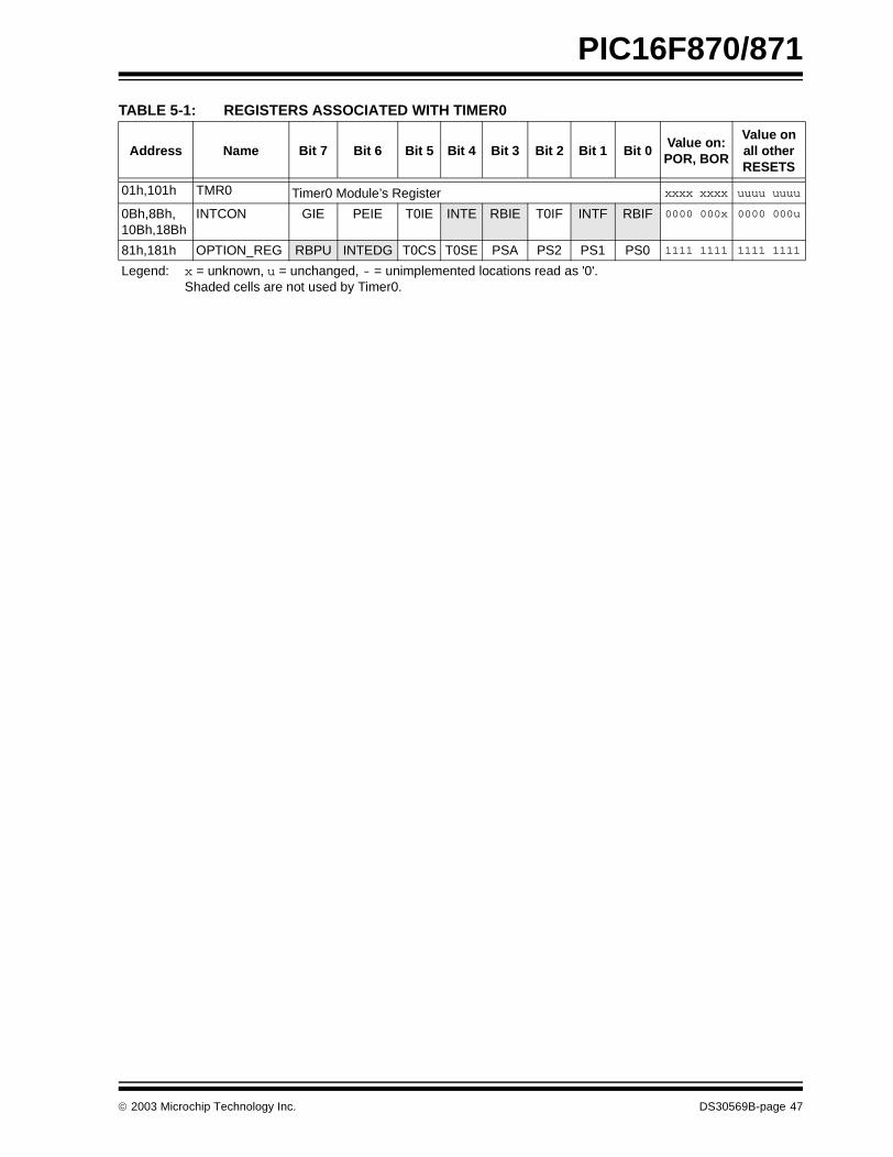
PIC16F870/871
TABLE 5-1: REGISTERS ASSOCIATED WITH TIMER0
Address Name Bit 7 Bit 6 Bit 5 Bit 4 Bit 3 Bit 2 Bit 1 Bit 0Value on: POR, BOR
Value on all other RESETS
01h,101h TMR0 Timer0 Module’s Register xxxx xxxx uuuu uuuu
0Bh,8Bh,10Bh,18Bh
INTCON GIE PEIE T0IE INTE RBIE T0IF INTF RBIF 0000 000x 0000 000u
81h,181h OPTION_REG RBPU INTEDG T0CS T0SE PSA PS2 PS1 PS0 1111 1111 1111 1111
Legend: x = unknown, u = unchanged, - = unimplemented locations read as '0'. Shaded cells are not used by Timer0.
2003 Microchip Technology Inc. DS30569B-page 47

PIC16F870/871
NOTES:
DS30569B-page 48 2003 Microchip Technology Inc.

PIC16F870/871
6.0 TIMER1 MODULE
The Timer1 module is a 16-bit timer/counter consistingof two 8-bit registers (TMR1H and TMR1L), which arereadable and writable. The TMR1 register pair(TMR1H:TMR1L) increments from 0000h to FFFFhand rolls over to 0000h. The TMR1 interrupt, if enabled,is generated on overflow, which is latched in interruptflag bit, TMR1IF (PIR1<0>). This interrupt can beenabled/disabled by setting/clearing TMR1 interruptenable bit, TMR1IE (PIE1<0>).
Timer1 can operate in one of two modes:
• As a timer• As a counter
The Operating mode is determined by the clock selectbit, TMR1CS (T1CON<1>).
In Timer mode, Timer1 increments every instructioncycle. In Counter mode, it increments on every risingedge of the external clock input.
Timer1 can be enabled/disabled by setting/clearingcontrol bit, TMR1ON (T1CON<0>).
Timer1 also has an internal “RESET input”. ThisRESET can be generated by either of the two CCPmodules (Section 8.0). Register 6-1 shows the Timer1control register.
When the Timer1 oscillator is enabled (T1OSCEN isset), the RC1/T1OSI and RC0/T1OSO/T1CKI pinsbecome inputs. That is, the TRISC<1:0> value isignored, and these pins read as ‘0’.
Additional information on timer modules is available inthe PICmicro™ Mid-Range MCU Family ReferenceManual (DS33023).
REGISTER 6-1: T1CON: TIMER1 CONTROL REGISTER (ADDRESS: 10h) U-0 U-0 R/W-0 R/W-0 R/W-0 R/W-0 R/W-0 R/W-0
— — T1CKPS1 T1CKPS0 T1OSCEN T1SYNC TMR1CS TMR1ON
bit 7 bit 0
bit 7-6 Unimplemented: Read as '0'
bit 5-4 T1CKPS1:T1CKPS0: Timer1 Input Clock Prescale Select bits
11 = 1:8 Prescale value10 = 1:4 Prescale value01 = 1:2 Prescale value00 = 1:1 Prescale value
bit 3 T1OSCEN: Timer1 Oscillator Enable Control bit
1 = Oscillator is enabled0 = Oscillator is shut-off (the oscillator inverter is turned off to eliminate power drain)
bit 2 T1SYNC: Timer1 External Clock Input Synchronization Control bitWhen TMR1CS = 1:1 = Do not synchronize external clock input0 = Synchronize external clock inputWhen TMR1CS = 0:This bit is ignored. Timer1 uses the internal clock when TMR1CS = 0.
bit 1 TMR1CS: Timer1 Clock Source Select bit
1 = External clock from pin RC0/T1OSO/T1CKI (on the rising edge)0 = Internal clock (FOSC/4)
bit 0 TMR1ON: Timer1 On bit1 = Enables Timer10 = Stops Timer1
Legend:
R = Readable bit W = Writable bit U = Unimplemented bit, read as ‘0’
- n = Value at POR ‘1’ = Bit is set ‘0’ = Bit is cleared x = Bit is unknown
2003 Microchip Technology Inc. DS30569B-page 49
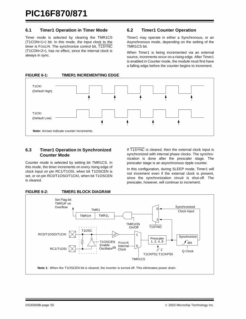
PIC16F870/871
6.1 Timer1 Operation in Timer Mode
Timer mode is selected by clearing the TMR1CS(T1CON<1>) bit. In this mode, the input clock to thetimer is FOSC/4. The synchronize control bit, T1SYNC(T1CON<2>), has no effect, since the internal clock isalways in sync.
6.2 Timer1 Counter Operation
Timer1 may operate in either a Synchronous, or anAsynchronous mode, depending on the setting of theTMR1CS bit.
When Timer1 is being incremented via an externalsource, increments occur on a rising edge. After Timer1is enabled in Counter mode, the module must first havea falling edge before the counter begins to increment.
FIGURE 6-1: TIMER1 INCREMENTING EDGE
6.3 Timer1 Operation in Synchronized Counter Mode
Counter mode is selected by setting bit TMR1CS. Inthis mode, the timer increments on every rising edge ofclock input on pin RC1/T1OSI, when bit T1OSCEN isset, or on pin RC0/T1OSO/T1CKI, when bit T1OSCENis cleared.
If T1SYNC is cleared, then the external clock input issynchronized with internal phase clocks. The synchro-nization is done after the prescaler stage. Theprescaler stage is an asynchronous ripple counter.
In this configuration, during SLEEP mode, Timer1 willnot increment even if the external clock is present,since the synchronization circuit is shut-off. Theprescaler, however, will continue to increment.
FIGURE 6-2: TIMER1 BLOCK DIAGRAM
T1CKI
(Default High)
T1CKI
(Default Low)
Note: Arrows indicate counter increments.
TMR1H TMR1L
T1OSCT1SYNC
TMR1CS
T1CKPS1:T1CKPS0Q Clock
T1OSCENEnableOscillator(1)
FOSC/4InternalClock
TMR1ONOn/Off
Prescaler1, 2, 4, 8
Synchronize
det
1
0
0
1
SynchronizedClock Input
2
RC0/T1OSO/T1CKI
RC1/T1OSI
Note 1: When the T1OSCEN bit is cleared, the inverter is turned off. This eliminates power drain.
Set Flag bitTMR1IF onOverflow
TMR1
DS30569B-page 50 2003 Microchip Technology Inc.
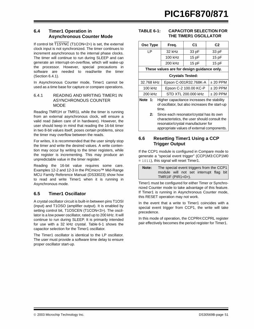
PIC16F870/871
6.4 Timer1 Operation in Asynchronous Counter Mode
If control bit T1SYNC (T1CON<2>) is set, the externalclock input is not synchronized. The timer continues toincrement asynchronous to the internal phase clocks.The timer will continue to run during SLEEP and cangenerate an interrupt-on-overflow, which will wake-upthe processor. However, special precautions insoftware are needed to read/write the timer(Section 6.4.1).
In Asynchronous Counter mode, Timer1 cannot beused as a time base for capture or compare operations.
6.4.1 READING AND WRITING TIMER1 IN ASYNCHRONOUS COUNTER MODE
Reading TMR1H or TMR1L while the timer is runningfrom an external asynchronous clock, will ensure avalid read (taken care of in hardware). However, theuser should keep in mind that reading the 16-bit timerin two 8-bit values itself, poses certain problems, sincethe timer may overflow between the reads.
For writes, it is recommended that the user simply stopthe timer and write the desired values. A write conten-tion may occur by writing to the timer registers, whilethe register is incrementing. This may produce anunpredictable value in the timer register.
Reading the 16-bit value requires some care.Examples 12-2 and 12-3 in the PICmicro™ Mid-RangeMCU Family Reference Manual (DS33023) show howto read and write Timer1 when it is running inAsynchronous mode.
6.5 Timer1 Oscillator
A crystal oscillator circuit is built-in between pins T1OSI(input) and T1OSO (amplifier output). It is enabled bysetting control bit, T1OSCEN (T1CON<3>). The oscil-lator is a low power oscillator, rated up to 200 kHz. It willcontinue to run during SLEEP. It is primarily intendedfor use with a 32 kHz crystal. Table 6-1 shows thecapacitor selection for the Timer1 oscillator.
The Timer1 oscillator is identical to the LP oscillator.The user must provide a software time delay to ensureproper oscillator start-up.
TABLE 6-1: CAPACITOR SELECTION FOR THE TIMER1 OSCILLATOR
6.6 Resetting Timer1 Using a CCP Trigger Output
If the CCP1 module is configured in Compare mode togenerate a “special event trigger” (CCP1M3:CCP1M0= 1011), this signal will reset Timer1.
Timer1 must be configured for either Timer or Synchro-nized Counter mode to take advantage of this feature.If Timer1 is running in Asynchronous Counter mode,this RESET operation may not work.
In the event that a write to Timer1 coincides with aspecial event trigger from CCP1, the write will takeprecedence.
In this mode of operation, the CCPRH:CCPRL registerpair effectively becomes the period register for Timer1.
Osc Type Freq. C1 C2
LP 32 kHz 33 pF 33 pF
100 kHz 15 pF 15 pF
200 kHz 15 pF 15 pF
These values are for design guidance only.
Crystals Tested:
32.768 kHz Epson C-001R32.768K-A ± 20 PPM
100 kHz Epson C-2 100.00 KC-P ± 20 PPM
200 kHz STD XTL 200.000 kHz ± 20 PPM
Note 1: Higher capacitance increases the stability of oscillator, but also increases the start-up time.
2: Since each resonator/crystal has its own characteristics, the user should consult the resonator/crystal manufacturer for appropriate values of external components.
Note: The special event triggers from the CCP1module will not set interrupt flag bitTMR1IF (PIR1<0>).
2003 Microchip Technology Inc. DS30569B-page 51
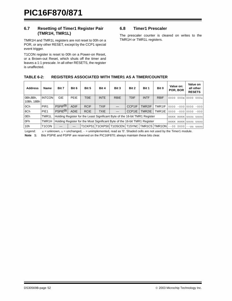
PIC16F870/871
6.7 Resetting of Timer1 Register Pair (TMR1H, TMR1L)
TMR1H and TMR1L registers are not reset to 00h on aPOR, or any other RESET, except by the CCP1 specialevent trigger.
T1CON register is reset to 00h on a Power-on Reset,or a Brown-out Reset, which shuts off the timer andleaves a 1:1 prescale. In all other RESETS, the registeris unaffected.
6.8 Timer1 Prescaler
The prescaler counter is cleared on writes to theTMR1H or TMR1L registers.
TABLE 6-2: REGISTERS ASSOCIATED WITH TIMER1 AS A TIMER/COUNTER
Address Name Bit 7 Bit 6 Bit 5 Bit 4 Bit 3 Bit 2 Bit 1 Bit 0Value on:POR, BOR
Value on all other RESETS
0Bh,8Bh,10Bh, 18Bh
INTCON GIE PEIE T0IE INTE RBIE T0IF INTF RBIF 0000 000x 0000 000u
0Ch PIR1 PSPIF(1) ADIF RCIF TXIF — CCP1IF TMR2IF TMR1IF 0000 -000 0000 -000
8Ch PIE1 PSPIE(1) ADIE RCIE TXIE — CCP1IE TMR2IE TMR1IE 0000 -000 0000 -000
0Eh TMR1L Holding Register for the Least Significant Byte of the 16-bit TMR1 Register xxxx xxxx uuuu uuuu
0Fh TMR1H Holding Register for the Most Significant Byte of the 16-bit TMR1 Register xxxx xxxx uuuu uuuu
10h T1CON — — T1CKPS1 T1CKPS0 T1OSCEN T1SYNC TMR1CS TMR1ON --00 0000 --uu uuuu
Legend: x = unknown, u = unchanged, - = unimplemented, read as '0'. Shaded cells are not used by the Timer1 module.Note 1: Bits PSPIE and PSPIF are reserved on the PIC16F870; always maintain these bits clear.
DS30569B-page 52 2003 Microchip Technology Inc.
PIC16F870/871
7.0 TIMER2 MODULE
Timer2 is an 8-bit timer with a prescaler and apostscaler. It can be used as the PWM time base for thePWM mode of the CCP module(s). The TMR2 registeris readable and writable, and is cleared on any deviceRESET.
The input clock (FOSC/4) has a prescale option of 1:1,1:4, or 1:16, selected by control bitsT2CKPS1:T2CKPS0 (T2CON<1:0>).
The Timer2 module has an 8-bit period register, PR2.Timer2 increments from 00h until it matches PR2 andthen resets to 00h on the next increment cycle. PR2 isa readable and writable register. The PR2 register isinitialized to FFh upon RESET.
The match output of TMR2 goes through a 4-bitpostscaler (which gives a 1:1 to 1:16 scaling inclusive)to generate a TMR2 interrupt (latched in flag bitTMR2IF (PIR1<1>)).
Timer2 can be shut-off by clearing control bit, TMR2ON(T2CON<2>), to minimize power consumption.
Register 7-1 shows the Timer2 control register.
Additional information on timer modules is available inthe PICmicro™ Mid-Range MCU Family ReferenceManual (DS33023).
FIGURE 7-1: TIMER2 BLOCK DIAGRAM
REGISTER 7-1: T2CON: TIMER2 CONTROL REGISTER (ADDRESS 12h)
Comparator
TMR2Sets Flag
TMR2 Reg
Output(1)
RESET
Postscaler
Prescaler
PR2 Reg
2
FOSC/4
1:1 1:16
1:1, 1:4, 1:16
EQ
4
bit TMR2IF
Note 1: TMR2 register output can be software selected by the SSP module as a baud clock.
to
T2OUTPS3:T2OUTPS0
T2CKPS1:T2CKPS0
U-0 R/W-0 R/W-0 R/W-0 R/W-0 R/W-0 R/W-0 R/W-0
— TOUTPS3 TOUTPS2 TOUTPS1 TOUTPS0 TMR2ON T2CKPS1 T2CKPS0
bit 7 bit 0
bit 7 Unimplemented: Read as '0'
bit 6-3 TOUTPS3:TOUTPS0: Timer2 Output Postscale Select bits0000 = 1:1 Postscale0001 = 1:2 Postscale0010 = 1:3 Postscale•••1111 = 1:16 Postscale
bit 2 TMR2ON: Timer2 On bit1 = Timer2 is on0 = Timer2 is off
bit 1-0 T2CKPS1:T2CKPS0: Timer2 Clock Prescale Select bits00 = Prescaler is 101 = Prescaler is 41x = Prescaler is 16
Legend:
R = Readable bit W = Writable bit U = Unimplemented bit, read as ‘0’
- n = Value at POR ‘1’ = Bit is set ‘0’ = Bit is cleared x = Bit is unknown
2003 Microchip Technology Inc. DS30569B-page 53
PIC16F870/871
7.1 Timer2 Prescaler and Postscaler
The prescaler and postscaler counters are clearedwhen any of the following occurs:
• a write to the TMR2 register• a write to the T2CON register
• any device RESET (POR, MCLR Reset, WDT Reset, or BOR)
TMR2 is not cleared when T2CON is written.
7.2 Output of TMR2
The output of TMR2 (before the postscaler) is fed to theSSP module, which optionally uses it to generate shiftclock.
TABLE 7-1: REGISTERS ASSOCIATED WITH TIMER2 AS A TIMER/COUNTER
Address Name Bit 7 Bit 6 Bit 5 Bit 4 Bit 3 Bit 2 Bit 1 Bit 0Value on:POR, BOR
Value on all other RESETS
0Bh,8Bh,10Bh,18Bh
INTCON GIE PEIE T0IE INTE RBIE T0IF INTF RBIF 0000 000x 0000 000u
0Ch PIR1 PSPIF(1) ADIF RCIF TXIF — CCP1IF TMR2IF TMR1IF 0000 -000 0000 -000
8Ch PIE1 PSPIE(1) ADIE RCIE TXIE — CCP1IE TMR2IE TMR1IE 0000 -000 0000 -000
11h TMR2 Timer2 Module’s Register 0000 0000 0000 0000
12h T2CON — TOUTPS3 TOUTPS2 TOUTPS1 TOUTPS0 TMR2ON T2CKPS1 T2CKPS0 -000 0000 -000 0000
92h PR2 Timer2 Period Register 1111 1111 1111 1111
Legend: x = unknown, u = unchanged, - = unimplemented, read as '0'. Shaded cells are not used by the Timer2 module.Note 1: Bits PSPIE and PSPIF are reserved on the PIC16F870; always maintain these bits clear.
DS30569B-page 54 2003 Microchip Technology Inc.
PIC16F870/871
8.0 CAPTURE/COMPARE/PWM MODULES
Each Capture/Compare/PWM (CCP) module containsa 16-bit register which can operate as a:
• 16-bit Capture register• 16-bit Compare register
• PWM Master/Slave Duty Cycle register
Table 8-1 shows the resources and interactions of theCCP module. In the following sections, the operation ofa CCP module is described.
8.1 CCP1 Module
Capture/Compare/PWM Register1 (CCPR1) is com-prised of two 8-bit registers: CCPR1L (low byte) andCCPR1H (high byte). The CCP1CON register controlsthe operation of CCP1. The special event trigger isgenerated by a compare match and will reset Timer1and start an A/D conversion (if the A/D module isenabled).
Additional information on CCP modules is available inthe PICmicro™ Mid-Range MCU Family ReferenceManual (DS33023) and in application note AN594,“Using the CCP Modules” (DS00594).
TABLE 8-1: CCP MODE - TIMER RESOURCES REQUIRED
REGISTER 8-1: CCP1CON REGISTER REGISTER (ADDRESS: 17h/1Dh)
CCP Mode Timer Resource
CaptureCompare
PWM
Timer1Timer1Timer2
U-0 U-0 R/W-0 R/W-0 R/W-0 R/W-0 R/W-0 R/W-0
— — CCP1X CCP1Y CCP1M3 CCP1M2 CCP1M1 CCP1M0
bit 7 bit 0
bit 7-6 Unimplemented: Read as '0'
bit 5-4 CCP1X:CCP1Y: PWM Least Significant bitsCapture mode:UnusedCompare mode:UnusedPWM mode:These bits are the two LSbs of the PWM duty cycle. The eight MSbs are found in CCPR1L.
bit 3-0 CCP1M3:CCP1M0: CCP1 Mode Select bits0000 = Capture/Compare/PWM disabled (resets CCP1 module)0100 = Capture mode, every falling edge0101 = Capture mode, every rising edge0110 = Capture mode, every 4th rising edge0111 = Capture mode, every 16th rising edge1000 = Compare mode, set output on match (CCP1IF bit is set)1001 = Compare mode, clear output on match (CCP1IF bit is set)1010 = Compare mode, generate software interrupt on match (CCP1IF bit is set, CCP1 pin is
unaffected)1011 = Compare mode, trigger special event (CCP1IF bit is set, CCP1 pin is unaffected);
CCP1resets TMR1, and starts an A/D conversion (if A/D module is enabled)11xx = PWM mode
Legend:
R = Readable bit W = Writable bit U = Unimplemented bit, read as ‘0’
- n = Value at POR ‘1’ = Bit is set ‘0’ = Bit is cleared x = Bit is unknown
2003 Microchip Technology Inc. DS30569B-page 55
PIC16F870/871
8.2 Capture Mode
In Capture mode, CCPR1H:CCPR1L captures the16-bit value of the TMR1 register when an event occurson pin RC2/CCP1. An event is defined as one of thefollowing:
• Every falling edge
• Every rising edge• Every 4th rising edge• Every 16th rising edge
The type of event is configured by control bitsCCP1M3:CCP1M0 (CCP1CON<3:0>). When a cap-ture is made, the interrupt request flag bit CCP1IF(PIR1<2>) is set. The interrupt flag must be cleared insoftware. If another capture occurs before the value inregister CCPR1 is read, the old captured value isoverwritten by the new value.
8.2.1 CCP PIN CONFIGURATION
In Capture mode, the RC2/CCP1 pin should beconfigured as an input by setting the TRISC<2> bit.
FIGURE 8-1: CAPTURE MODE OPERATION BLOCK DIAGRAM
8.2.2 TIMER1 MODE SELECTION
Timer1 must be running in Timer mode, or Synchro-nized Counter mode, for the CCP module to use thecapture feature. In Asynchronous Counter mode, thecapture operation may not work.
8.2.3 SOFTWARE INTERRUPT
When the Capture mode is changed, a false captureinterrupt may be generated. The user should keep bitCCP1IE (PIE1<2>) clear to avoid false interrupts andshould clear the flag bit, CCP1IF, following any suchchange in Operating mode.
8.2.4 CCP PRESCALER
There are four prescaler settings, specified by bitsCCP1M3:CCP1M0. Whenever the CCP module isturned off, or the CCP module is not in Capture mode,the prescaler counter is cleared. Any RESET will clearthe prescaler counter.
Switching from one capture prescaler to another maygenerate an interrupt. Also, the prescaler counter willnot be cleared, therefore, the first capture may be froma non-zero prescaler. Example 8-1 shows the recom-mended method for switching between capture pres-calers. This example also clears the prescaler counterand will not generate the “false” interrupt.
EXAMPLE 8-1: CHANGING BETWEEN CAPTURE PRESCALERS
Note: If the RC2/CCP1 pin is configured as anoutput, a write to the port can cause acapture condition.
CCPR1H CCPR1L
TMR1H TMR1L
Set Flag bit CCP1IF(PIR1<2>)
CaptureEnable
QsCCP1CON<3:0>
RC2/CCP1
Prescaler÷ 1, 4, 16
andEdge Detect
pin CLRF CCP1CON ; Turn CCP module offMOVLW NEW_CAPT_PS ; Load the W reg with
; the new prescaler; move value and CCP ON
MOVWF CCP1CON ; Load CCP1CON with this; value
DS30569B-page 56 2003 Microchip Technology Inc.

PIC16F870/871
8.3 Compare Mode
In Compare mode, the 16-bit CCPR1 register value isconstantly compared against the TMR1 register pairvalue. When a match occurs, the RC2/CCP1 pin is:
• Driven high• Driven low• Remains unchanged
The action on the pin is based on the value of controlbits, CCP1M3:CCP1M0 (CCP1CON<3:0>). At thesame time, interrupt flag bit CCP1IF is set.
FIGURE 8-2: COMPARE MODE OPERATION BLOCK DIAGRAM
8.3.1 CCP PIN CONFIGURATION
The user must configure the RC2/CCP1 pin as anoutput by clearing the TRISC<2> bit.
8.3.2 TIMER1 MODE SELECTION
Timer1 must be running in Timer mode, or Synchro-nized Counter mode, if the CCP module is using thecompare feature. In Asynchronous Counter mode, thecompare operation may not work.
8.3.3 SOFTWARE INTERRUPT MODE
When Generate Software Interrupt mode is chosen, theCCP1 pin is not affected. The CCPIF bit is set, causinga CCP interrupt (if enabled).
8.3.4 SPECIAL EVENT TRIGGER
In this mode, an internal hardware trigger is generated,which may be used to initiate an action.
The special event trigger output of CCP1 resets theTMR1 register pair, and starts an A/D conversion (if A/Dmodule is enabled). This allows the CCPR1 register toeffectively be a 16-bit programmable period register forTimer1.
Note: Clearing the CCP1CON register will forcethe RC2/CCP1 compare output latch tothe default low level. This is not thePORTC I/O data latch.
CCPR1H CCPR1L
TMR1H TMR1L
ComparatorQ S
R
OutputLogic
Special Event Trigger
Set Flag bit CCP1IF(PIR1<2>)
Match
RC2/CCP1
TRISC<2>CCP1CON<3:0>Mode Select
Output Enable
pin
Special event trigger will:reset Timer1, but not set interrupt flag bit TMR1IF (PIR1<0>),and set bit GO/DONE (ADCON0<2>).
Note: The special event trigger from the CCP1module will not set interrupt flag bitTMR1IF (PIR1<0>).
2003 Microchip Technology Inc. DS30569B-page 57

PIC16F870/871
8.4 PWM Mode (PWM)
In Pulse Width Modulation mode, the CCP1 pin pro-duces up to a 10-bit resolution PWM output. Since theCCP1 pin is multiplexed with the PORTC data latch, theTRISC<2> bit must be cleared to make the CCP1 pinan output.
Figure 8-3 shows a simplified block diagram of theCCP module in PWM mode.
For a step-by-step procedure on how to set up the CCPmodule for PWM operation, see Section 8.4.3.
FIGURE 8-3: SIMPLIFIED PWM BLOCK DIAGRAM
A PWM output (Figure 8-4) has a time base (period)and a time that the output stays high (duty cycle). Thefrequency of the PWM is the inverse of the period(1/period).
FIGURE 8-4: PWM OUTPUT
8.4.1 PWM PERIOD
The PWM period is specified by writing to the PR2register. The PWM period can be calculated using thefollowing formula:
PWM period = [(PR2) + 1] • 4 • TOSC •(TMR2 prescale value)
PWM frequency is defined as 1 / [PWM period].
When TMR2 is equal to PR2, the following three eventsoccur on the next increment cycle:
• TMR2 is cleared• The CCP1 pin is set (exception: if PWM duty
cycle = 0%, the CCP1 pin will not be set)• The PWM duty cycle is latched from CCPR1L into
CCPR1H
8.4.2 PWM DUTY CYCLE
The PWM duty cycle is specified by writing to theCCPR1L register and to the CCP1CON<5:4> bits. Upto 10-bit resolution is available. The CCPR1L containsthe eight MSbs and the CCP1CON<5:4> contains thetwo LSbs. This 10-bit value is represented byCCPR1L:CCP1CON<5:4>. The following equation isused to calculate the PWM duty cycle in time:
PWM duty cycle = (CCPR1L:CCP1CON<5:4>) • TOSC • (TMR2 prescale value)
CCPR1L and CCP1CON<5:4> can be written to at anytime, but the duty cycle value is not latched intoCCPR1H until after a match between PR2 and TMR2occurs (i.e., the period is complete). In PWM mode,CCPR1H is a read-only register.
The CCPR1H register and a 2-bit internal latch areused to double buffer the PWM duty cycle. This doublebuffering is essential for glitch-free PWM operation.
When the CCPR1H and 2-bit latch match TMR2, con-catenated with an internal 2-bit Q clock, or 2 bits of theTMR2 prescaler, the CCP1 pin is cleared.
The maximum PWM resolution (bits) for a given PWMfrequency is given by the formula:
Note: Clearing the CCP1CON register will forcethe CCP1 PWM output latch to the defaultlow level. This is not the PORTC I/O datalatch.
CCPR1L
CCPR1H (Slave)
Comparator
TMR2
Comparator
PR2
(Note 1)
R Q
S
Duty Cycle Registers CCP1CON<5:4>
Clear Timer,CCP1 pin and latch D.C.
TRISC<2>
RC2/CCP1
Note 1: The 8-bit timer is concatenated with 2-bit internal Q clock, or 2 bits of the prescaler, to create 10-bit time base.
Period
Duty Cycle
TMR2 = PR2
TMR2 = Duty Cycle
TMR2 = PR2
Note: The Timer2 postscaler (see Section 7.1) isnot used in the determination of the PWMfrequency. The postscaler could be usedto have a servo update rate at a differentfrequency than the PWM output.
Note: If the PWM duty cycle value is longer thanthe PWM period, the CCP1 pin will not becleared.
log(FPWM
log(2)
FOSC )bits=Resolution
DS30569B-page 58 2003 Microchip Technology Inc.
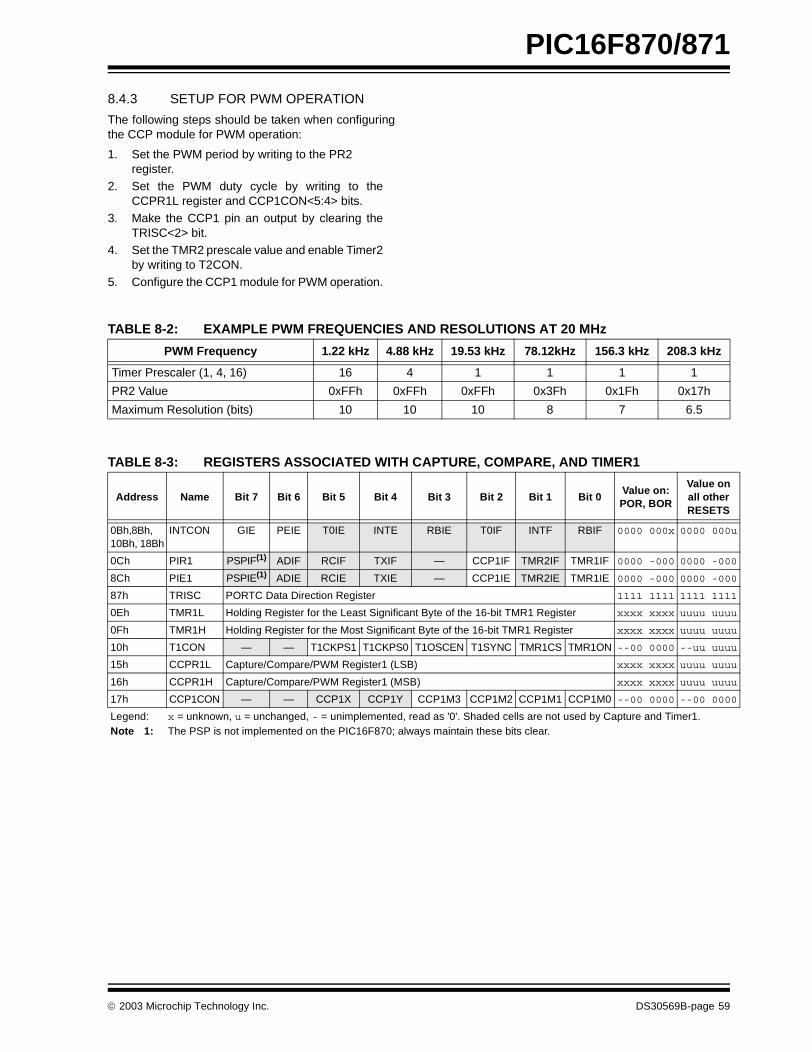
PIC16F870/871
8.4.3 SETUP FOR PWM OPERATION
The following steps should be taken when configuringthe CCP module for PWM operation:
1. Set the PWM period by writing to the PR2 register.
2. Set the PWM duty cycle by writing to theCCPR1L register and CCP1CON<5:4> bits.
3. Make the CCP1 pin an output by clearing theTRISC<2> bit.
4. Set the TMR2 prescale value and enable Timer2by writing to T2CON.
5. Configure the CCP1 module for PWM operation.
TABLE 8-2: EXAMPLE PWM FREQUENCIES AND RESOLUTIONS AT 20 MHz
TABLE 8-3: REGISTERS ASSOCIATED WITH CAPTURE, COMPARE, AND TIMER1
PWM Frequency 1.22 kHz 4.88 kHz 19.53 kHz 78.12kHz 156.3 kHz 208.3 kHz
Timer Prescaler (1, 4, 16) 16 4 1 1 1 1
PR2 Value 0xFFh 0xFFh 0xFFh 0x3Fh 0x1Fh 0x17h
Maximum Resolution (bits) 10 10 10 8 7 6.5
Address Name Bit 7 Bit 6 Bit 5 Bit 4 Bit 3 Bit 2 Bit 1 Bit 0Value on:POR, BOR
Value onall otherRESETS
0Bh,8Bh,10Bh, 18Bh
INTCON GIE PEIE T0IE INTE RBIE T0IF INTF RBIF 0000 000x 0000 000u
0Ch PIR1 PSPIF(1) ADIF RCIF TXIF — CCP1IF TMR2IF TMR1IF 0000 -000 0000 -000
8Ch PIE1 PSPIE(1) ADIE RCIE TXIE — CCP1IE TMR2IE TMR1IE 0000 -000 0000 -000
87h TRISC PORTC Data Direction Register 1111 1111 1111 1111
0Eh TMR1L Holding Register for the Least Significant Byte of the 16-bit TMR1 Register xxxx xxxx uuuu uuuu
0Fh TMR1H Holding Register for the Most Significant Byte of the 16-bit TMR1 Register xxxx xxxx uuuu uuuu
10h T1CON — — T1CKPS1 T1CKPS0 T1OSCEN T1SYNC TMR1CS TMR1ON --00 0000 --uu uuuu
15h CCPR1L Capture/Compare/PWM Register1 (LSB) xxxx xxxx uuuu uuuu
16h CCPR1H Capture/Compare/PWM Register1 (MSB) xxxx xxxx uuuu uuuu
17h CCP1CON — — CCP1X CCP1Y CCP1M3 CCP1M2 CCP1M1 CCP1M0 --00 0000 --00 0000
Legend: x = unknown, u = unchanged, - = unimplemented, read as '0'. Shaded cells are not used by Capture and Timer1.Note 1: The PSP is not implemented on the PIC16F870; always maintain these bits clear.
2003 Microchip Technology Inc. DS30569B-page 59
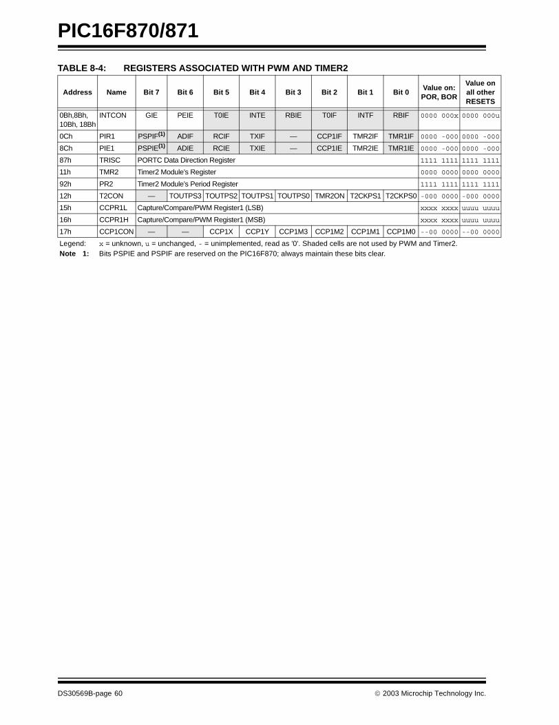
PIC16F870/871
u
0
0
1
0
1
0
u
u
0
TABLE 8-4: REGISTERS ASSOCIATED WITH PWM AND TIMER2
Address Name Bit 7 Bit 6 Bit 5 Bit 4 Bit 3 Bit 2 Bit 1 Bit 0Value on:POR, BOR
Value onall otherRESETS
0Bh,8Bh,10Bh, 18Bh
INTCON GIE PEIE T0IE INTE RBIE T0IF INTF RBIF 0000 000x 0000 000
0Ch PIR1 PSPIF(1) ADIF RCIF TXIF — CCP1IF TMR2IF TMR1IF 0000 -000 0000 -00
8Ch PIE1 PSPIE(1) ADIE RCIE TXIE — CCP1IE TMR2IE TMR1IE 0000 -000 0000 -00
87h TRISC PORTC Data Direction Register 1111 1111 1111 111
11h TMR2 Timer2 Module’s Register 0000 0000 0000 000
92h PR2 Timer2 Module’s Period Register 1111 1111 1111 111
12h T2CON — TOUTPS3 TOUTPS2 TOUTPS1 TOUTPS0 TMR2ON T2CKPS1 T2CKPS0 -000 0000 -000 000
15h CCPR1L Capture/Compare/PWM Register1 (LSB) xxxx xxxx uuuu uuu
16h CCPR1H Capture/Compare/PWM Register1 (MSB) xxxx xxxx uuuu uuu
17h CCP1CON — — CCP1X CCP1Y CCP1M3 CCP1M2 CCP1M1 CCP1M0 --00 0000 --00 000
Legend: x = unknown, u = unchanged, - = unimplemented, read as '0'. Shaded cells are not used by PWM and Timer2.Note 1: Bits PSPIE and PSPIF are reserved on the PIC16F870; always maintain these bits clear.
DS30569B-page 60 2003 Microchip Technology Inc.
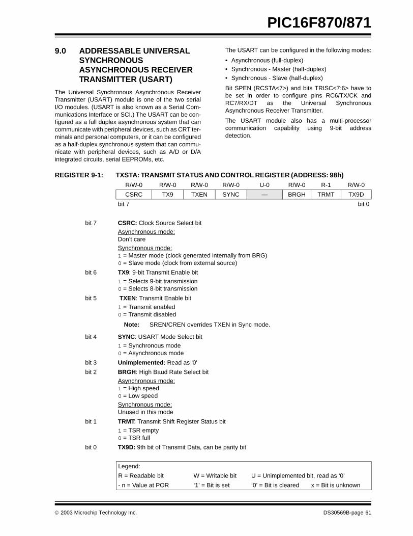
PIC16F870/871
9.0 ADDRESSABLE UNIVERSAL SYNCHRONOUS ASYNCHRONOUS RECEIVER TRANSMITTER (USART)
The Universal Synchronous Asynchronous ReceiverTransmitter (USART) module is one of the two serialI/O modules. (USART is also known as a Serial Com-munications Interface or SCI.) The USART can be con-figured as a full duplex asynchronous system that cancommunicate with peripheral devices, such as CRT ter-minals and personal computers, or it can be configuredas a half-duplex synchronous system that can commu-nicate with peripheral devices, such as A/D or D/Aintegrated circuits, serial EEPROMs, etc.
The USART can be configured in the following modes:
• Asynchronous (full-duplex)• Synchronous - Master (half-duplex)
• Synchronous - Slave (half-duplex)
Bit SPEN (RCSTA<7>) and bits TRISC<7:6> have tobe set in order to configure pins RC6/TX/CK andRC7/RX/DT as the Universal SynchronousAsynchronous Receiver Transmitter.
The USART module also has a multi-processorcommunication capability using 9-bit addressdetection.
REGISTER 9-1: TXSTA: TRANSMIT STATUS AND CONTROL REGISTER (ADDRESS: 98h) R/W-0 R/W-0 R/W-0 R/W-0 U-0 R/W-0 R-1 R/W-0
CSRC TX9 TXEN SYNC — BRGH TRMT TX9D
bit 7 bit 0
bit 7 CSRC: Clock Source Select bitAsynchronous mode:Don’t careSynchronous mode:1 = Master mode (clock generated internally from BRG)0 = Slave mode (clock from external source)
bit 6 TX9: 9-bit Transmit Enable bit
1 = Selects 9-bit transmission0 = Selects 8-bit transmission
bit 5 TXEN: Transmit Enable bit1 = Transmit enabled0 = Transmit disabled
Note: SREN/CREN overrides TXEN in Sync mode.
bit 4 SYNC: USART Mode Select bit1 = Synchronous mode0 = Asynchronous mode
bit 3 Unimplemented: Read as '0'
bit 2 BRGH: High Baud Rate Select bit
Asynchronous mode:1 = High speed0 = Low speedSynchronous mode:Unused in this mode
bit 1 TRMT: Transmit Shift Register Status bit1 = TSR empty0 = TSR full
bit 0 TX9D: 9th bit of Transmit Data, can be parity bit
Legend:
R = Readable bit W = Writable bit U = Unimplemented bit, read as ‘0’
- n = Value at POR ‘1’ = Bit is set ‘0’ = Bit is cleared x = Bit is unknown
2003 Microchip Technology Inc. DS30569B-page 61
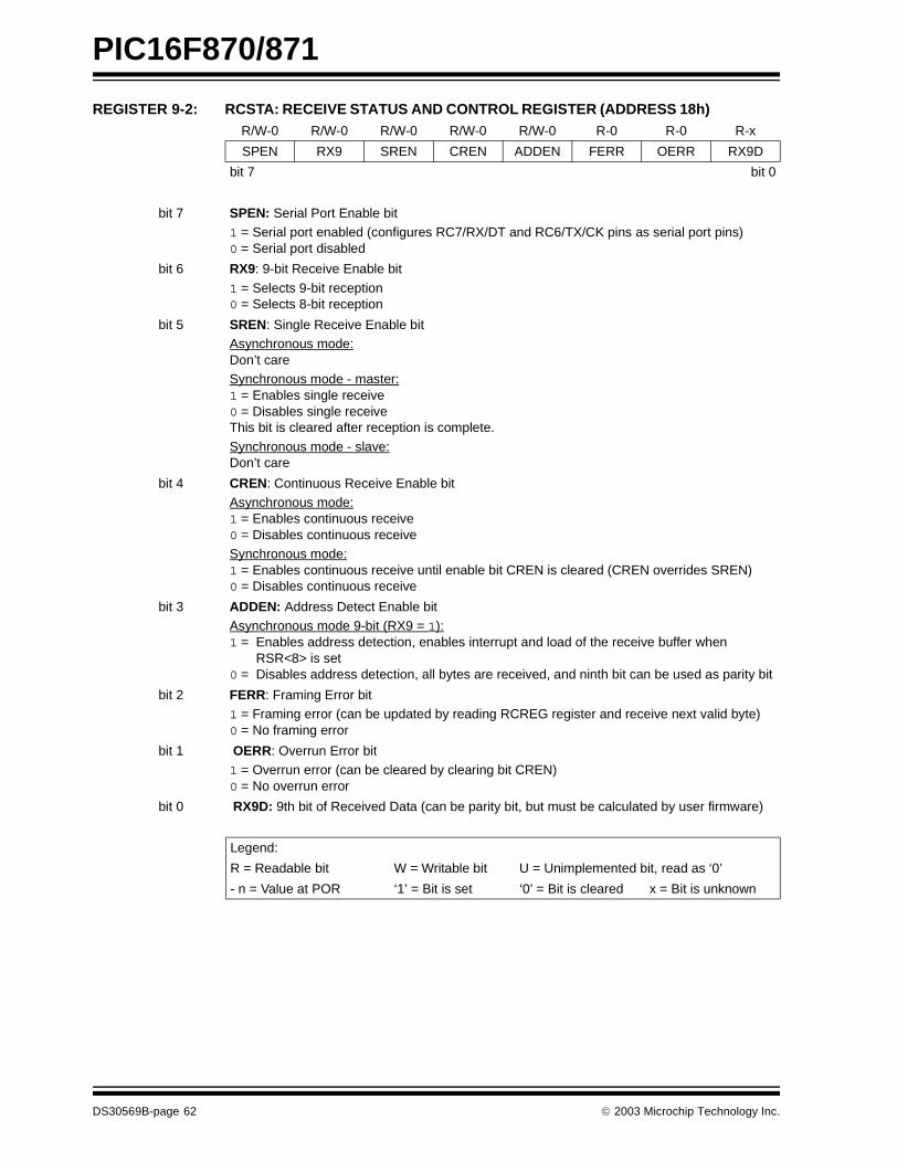
PIC16F870/871
REGISTER 9-2: RCSTA: RECEIVE STATUS AND CONTROL REGISTER (ADDRESS 18h) R/W-0 R/W-0 R/W-0 R/W-0 R/W-0 R-0 R-0 R-x
SPEN RX9 SREN CREN ADDEN FERR OERR RX9D
bit 7 bit 0
bit 7 SPEN: Serial Port Enable bit1 = Serial port enabled (configures RC7/RX/DT and RC6/TX/CK pins as serial port pins)0 = Serial port disabled
bit 6 RX9: 9-bit Receive Enable bit
1 = Selects 9-bit reception0 = Selects 8-bit reception
bit 5 SREN: Single Receive Enable bitAsynchronous mode:Don’t careSynchronous mode - master:1 = Enables single receive0 = Disables single receiveThis bit is cleared after reception is complete.
Synchronous mode - slave:Don’t care
bit 4 CREN: Continuous Receive Enable bitAsynchronous mode:1 = Enables continuous receive0 = Disables continuous receiveSynchronous mode:1 = Enables continuous receive until enable bit CREN is cleared (CREN overrides SREN)0 = Disables continuous receive
bit 3 ADDEN: Address Detect Enable bitAsynchronous mode 9-bit (RX9 = 1):1 = Enables address detection, enables interrupt and load of the receive buffer when
RSR<8> is set0 = Disables address detection, all bytes are received, and ninth bit can be used as parity bit
bit 2 FERR: Framing Error bit1 = Framing error (can be updated by reading RCREG register and receive next valid byte)0 = No framing error
bit 1 OERR: Overrun Error bit1 = Overrun error (can be cleared by clearing bit CREN)0 = No overrun error
bit 0 RX9D: 9th bit of Received Data (can be parity bit, but must be calculated by user firmware)
Legend:
R = Readable bit W = Writable bit U = Unimplemented bit, read as ‘0’
- n = Value at POR ‘1’ = Bit is set ‘0’ = Bit is cleared x = Bit is unknown
DS30569B-page 62 2003 Microchip Technology Inc.
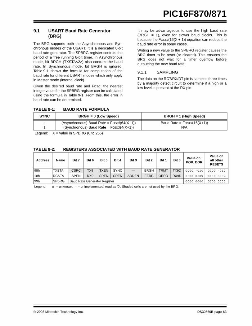
PIC16F870/871
9.1 USART Baud Rate Generator (BRG)
The BRG supports both the Asynchronous and Syn-chronous modes of the USART. It is a dedicated 8-bitbaud rate generator. The SPBRG register controls theperiod of a free running 8-bit timer. In Asynchronousmode, bit BRGH (TXSTA<2>) also controls the baudrate. In Synchronous mode, bit BRGH is ignored.Table 9-1 shows the formula for computation of thebaud rate for different USART modes which only applyin Master mode (internal clock).
Given the desired baud rate and FOSC, the nearestinteger value for the SPBRG register can be calculatedusing the formula in Table 9-1. From this, the error inbaud rate can be determined.
It may be advantageous to use the high baud rate(BRGH = 1), even for slower baud clocks. This isbecause the FOSC/(16(X + 1)) equation can reduce thebaud rate error in some cases.
Writing a new value to the SPBRG register causes theBRG timer to be reset (or cleared). This ensures theBRG does not wait for a timer overflow beforeoutputting the new baud rate.
9.1.1 SAMPLING
The data on the RC7/RX/DT pin is sampled three timesby a majority detect circuit to determine if a high or alow level is present at the RX pin.
TABLE 9-1: BAUD RATE FORMULA
TABLE 9-2: REGISTERS ASSOCIATED WITH BAUD RATE GENERATOR
SYNC BRGH = 0 (Low Speed) BRGH = 1 (High Speed)
01
(Asynchronous) Baud Rate = FOSC/(64(X+1))(Synchronous) Baud Rate = FOSC/(4(X+1))
Baud Rate = FOSC/(16(X+1))N/A
Legend: X = value in SPBRG (0 to 255)
Address Name Bit 7 Bit 6 Bit 5 Bit 4 Bit 3 Bit 2 Bit 1 Bit 0Value on: POR, BOR
Value on all other RESETS
98h TXSTA CSRC TX9 TXEN SYNC — BRGH TRMT TX9D 0000 -010 0000 -010
18h RCSTA SPEN RX9 SREN CREN ADDEN FERR OERR RX9D 0000 000x 0000 000x
99h SPBRG Baud Rate Generator Register 0000 0000 0000 0000
Legend: x = unknown, - = unimplemented, read as '0'. Shaded cells are not used by the BRG.
2003 Microchip Technology Inc. DS30569B-page 63
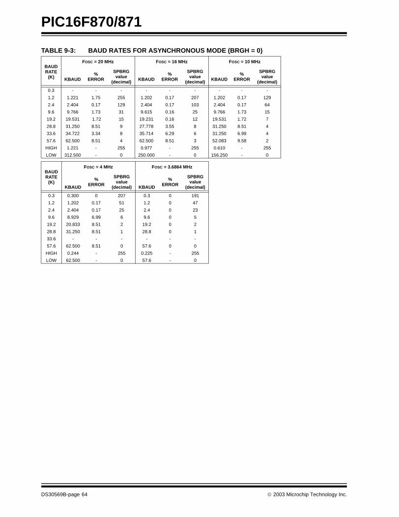
PIC16F870/871
TABLE 9-3: BAUD RATES FOR ASYNCHRONOUS MODE (BRGH = 0)
BAUDRATE
(K)
FOSC = 20 MHz FOSC = 16 MHz FOSC = 10 MHz
KBAUD%
ERROR
SPBRGvalue
(decimal) KBAUD%
ERROR
SPBRGvalue
(decimal) KBAUD%
ERROR
SPBRGvalue
(decimal)
0.3 - - - - - - - - -
1.2 1.221 1.75 255 1.202 0.17 207 1.202 0.17 129
2.4 2.404 0.17 129 2.404 0.17 103 2.404 0.17 64
9.6 9.766 1.73 31 9.615 0.16 25 9.766 1.73 15
19.2 19.531 1.72 15 19.231 0.16 12 19.531 1.72 7
28.8 31.250 8.51 9 27.778 3.55 8 31.250 8.51 4
33.6 34.722 3.34 8 35.714 6.29 6 31.250 6.99 4
57.6 62.500 8.51 4 62.500 8.51 3 52.083 9.58 2
HIGH 1.221 - 255 0.977 - 255 0.610 - 255
LOW 312.500 - 0 250.000 - 0 156.250 - 0
BAUDRATE
(K)
FOSC = 4 MHz FOSC = 3.6864 MHz
KBAUD
%ERROR
SPBRGvalue
(decimal) KBAUD
%ERROR
SPBRGvalue
(decimal)
0.3 0.300 0 207 0.3 0 191
1.2 1.202 0.17 51 1.2 0 47
2.4 2.404 0.17 25 2.4 0 23
9.6 8.929 6.99 6 9.6 0 5
19.2 20.833 8.51 2 19.2 0 2
28.8 31.250 8.51 1 28.8 0 1
33.6 - - - - - -
57.6 62.500 8.51 0 57.6 0 0
HIGH 0.244 - 255 0.225 - 255
LOW 62.500 - 0 57.6 - 0
DS30569B-page 64 2003 Microchip Technology Inc.
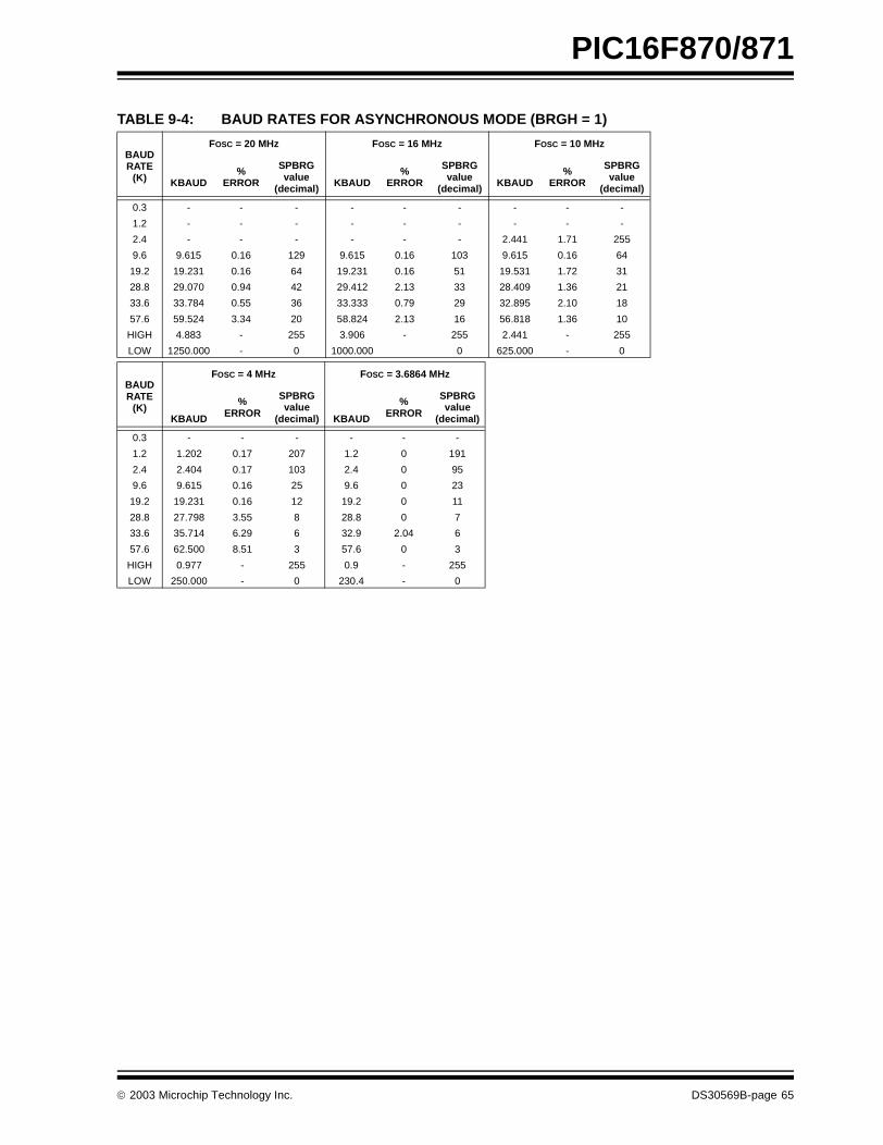
PIC16F870/871
TABLE 9-4: BAUD RATES FOR ASYNCHRONOUS MODE (BRGH = 1)
BAUDRATE
(K)
FOSC = 20 MHz FOSC = 16 MHz FOSC = 10 MHz
KBAUD%
ERROR
SPBRGvalue
(decimal) KBAUD%
ERROR
SPBRGvalue
(decimal) KBAUD%
ERROR
SPBRGvalue
(decimal)
0.3 - - - - - - - - -
1.2 - - - - - - - - -
2.4 - - - - - - 2.441 1.71 255
9.6 9.615 0.16 129 9.615 0.16 103 9.615 0.16 64
19.2 19.231 0.16 64 19.231 0.16 51 19.531 1.72 31
28.8 29.070 0.94 42 29.412 2.13 33 28.409 1.36 21
33.6 33.784 0.55 36 33.333 0.79 29 32.895 2.10 18
57.6 59.524 3.34 20 58.824 2.13 16 56.818 1.36 10
HIGH 4.883 - 255 3.906 - 255 2.441 - 255
LOW 1250.000 - 0 1000.000 0 625.000 - 0
BAUDRATE
(K)
FOSC = 4 MHz FOSC = 3.6864 MHz
KBAUD
%ERROR
SPBRGvalue
(decimal) KBAUD
%ERROR
SPBRGvalue
(decimal)
0.3 - - - - - -
1.2 1.202 0.17 207 1.2 0 191
2.4 2.404 0.17 103 2.4 0 95
9.6 9.615 0.16 25 9.6 0 23
19.2 19.231 0.16 12 19.2 0 11
28.8 27.798 3.55 8 28.8 0 7
33.6 35.714 6.29 6 32.9 2.04 6
57.6 62.500 8.51 3 57.6 0 3
HIGH 0.977 - 255 0.9 - 255
LOW 250.000 - 0 230.4 - 0
2003 Microchip Technology Inc. DS30569B-page 65
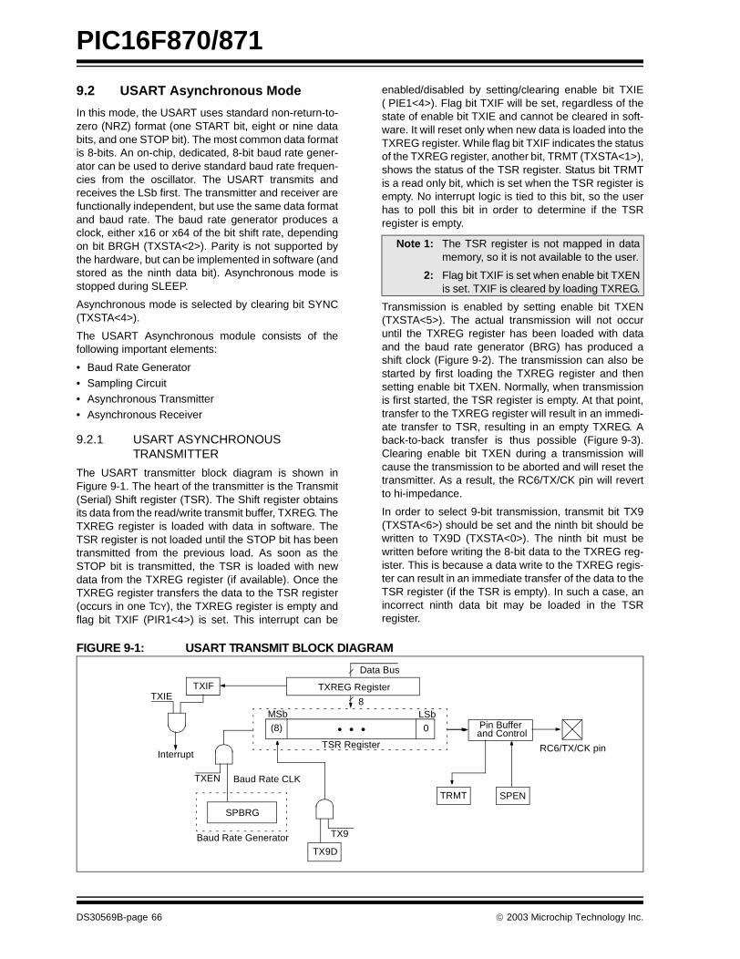
PIC16F870/871
9.2 USART Asynchronous Mode
In this mode, the USART uses standard non-return-to-zero (NRZ) format (one START bit, eight or nine databits, and one STOP bit). The most common data formatis 8-bits. An on-chip, dedicated, 8-bit baud rate gener-ator can be used to derive standard baud rate frequen-cies from the oscillator. The USART transmits andreceives the LSb first. The transmitter and receiver arefunctionally independent, but use the same data formatand baud rate. The baud rate generator produces aclock, either x16 or x64 of the bit shift rate, dependingon bit BRGH (TXSTA<2>). Parity is not supported bythe hardware, but can be implemented in software (andstored as the ninth data bit). Asynchronous mode isstopped during SLEEP.
Asynchronous mode is selected by clearing bit SYNC(TXSTA<4>).
The USART Asynchronous module consists of thefollowing important elements:
• Baud Rate Generator
• Sampling Circuit• Asynchronous Transmitter• Asynchronous Receiver
9.2.1 USART ASYNCHRONOUS TRANSMITTER
The USART transmitter block diagram is shown inFigure 9-1. The heart of the transmitter is the Transmit(Serial) Shift register (TSR). The Shift register obtainsits data from the read/write transmit buffer, TXREG. TheTXREG register is loaded with data in software. TheTSR register is not loaded until the STOP bit has beentransmitted from the previous load. As soon as theSTOP bit is transmitted, the TSR is loaded with newdata from the TXREG register (if available). Once theTXREG register transfers the data to the TSR register(occurs in one TCY), the TXREG register is empty andflag bit TXIF (PIR1<4>) is set. This interrupt can be
enabled/disabled by setting/clearing enable bit TXIE( PIE1<4>). Flag bit TXIF will be set, regardless of thestate of enable bit TXIE and cannot be cleared in soft-ware. It will reset only when new data is loaded into theTXREG register. While flag bit TXIF indicates the statusof the TXREG register, another bit, TRMT (TXSTA<1>),shows the status of the TSR register. Status bit TRMTis a read only bit, which is set when the TSR register isempty. No interrupt logic is tied to this bit, so the userhas to poll this bit in order to determine if the TSRregister is empty.
Transmission is enabled by setting enable bit TXEN(TXSTA<5>). The actual transmission will not occuruntil the TXREG register has been loaded with dataand the baud rate generator (BRG) has produced ashift clock (Figure 9-2). The transmission can also bestarted by first loading the TXREG register and thensetting enable bit TXEN. Normally, when transmissionis first started, the TSR register is empty. At that point,transfer to the TXREG register will result in an immedi-ate transfer to TSR, resulting in an empty TXREG. Aback-to-back transfer is thus possible (Figure 9-3).Clearing enable bit TXEN during a transmission willcause the transmission to be aborted and will reset thetransmitter. As a result, the RC6/TX/CK pin will revertto hi-impedance.
In order to select 9-bit transmission, transmit bit TX9(TXSTA<6>) should be set and the ninth bit should bewritten to TX9D (TXSTA<0>). The ninth bit must bewritten before writing the 8-bit data to the TXREG reg-ister. This is because a data write to the TXREG regis-ter can result in an immediate transfer of the data to theTSR register (if the TSR is empty). In such a case, anincorrect ninth data bit may be loaded in the TSRregister.
FIGURE 9-1: USART TRANSMIT BLOCK DIAGRAM
Note 1: The TSR register is not mapped in datamemory, so it is not available to the user.
2: Flag bit TXIF is set when enable bit TXENis set. TXIF is cleared by loading TXREG.
TXIFTXIE
Interrupt
TXEN Baud Rate CLK
SPBRG
Baud Rate GeneratorTX9D
MSb LSb
Data Bus
TXREG Register
TSR Register
(8) 0
TX9
TRMT SPEN
RC6/TX/CK pin
Pin Bufferand Control
8
• • •
DS30569B-page 66 2003 Microchip Technology Inc.
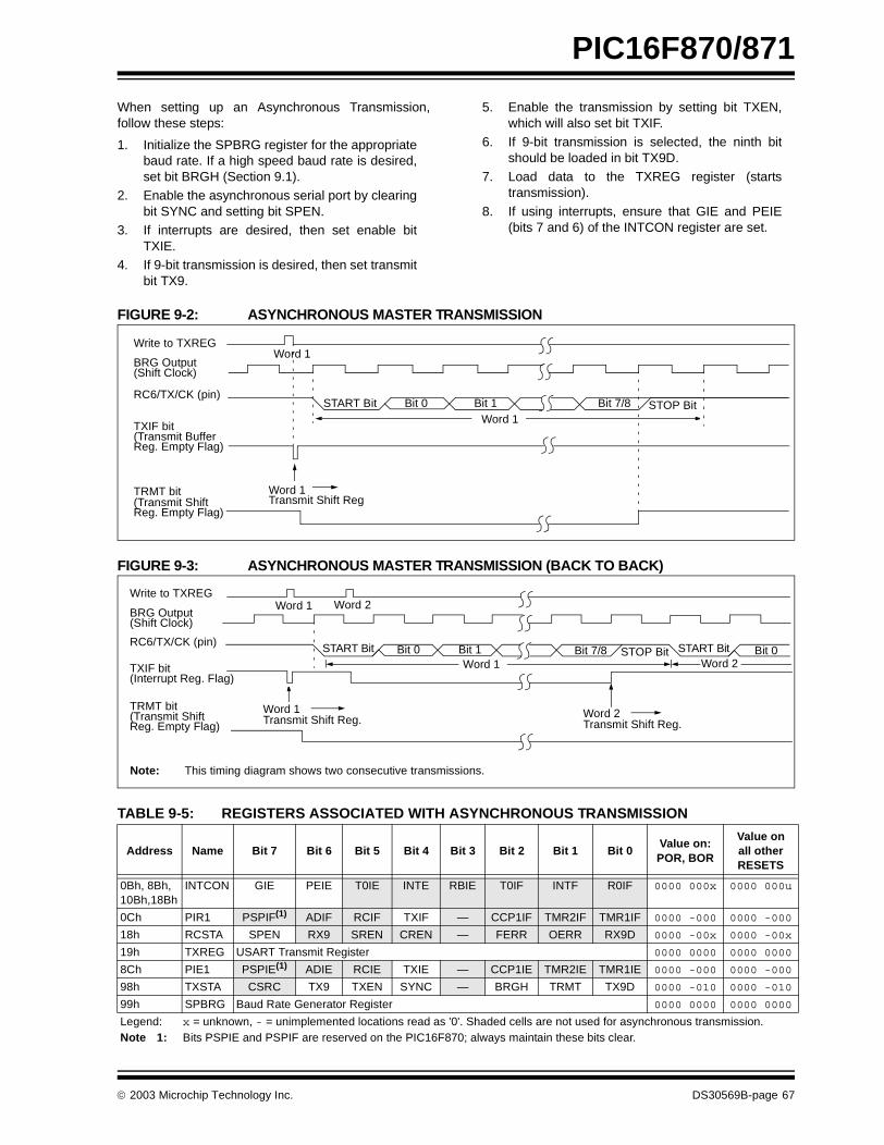
PIC16F870/871
When setting up an Asynchronous Transmission,follow these steps:
1. Initialize the SPBRG register for the appropriatebaud rate. If a high speed baud rate is desired,set bit BRGH (Section 9.1).
2. Enable the asynchronous serial port by clearingbit SYNC and setting bit SPEN.
3. If interrupts are desired, then set enable bitTXIE.
4. If 9-bit transmission is desired, then set transmitbit TX9.
5. Enable the transmission by setting bit TXEN,which will also set bit TXIF.
6. If 9-bit transmission is selected, the ninth bitshould be loaded in bit TX9D.
7. Load data to the TXREG register (startstransmission).
8. If using interrupts, ensure that GIE and PEIE(bits 7 and 6) of the INTCON register are set.
FIGURE 9-2: ASYNCHRONOUS MASTER TRANSMISSION
FIGURE 9-3: ASYNCHRONOUS MASTER TRANSMISSION (BACK TO BACK)
TABLE 9-5: REGISTERS ASSOCIATED WITH ASYNCHRONOUS TRANSMISSION
Address Name Bit 7 Bit 6 Bit 5 Bit 4 Bit 3 Bit 2 Bit 1 Bit 0Value on:POR, BOR
Value onall otherRESETS
0Bh, 8Bh, 10Bh,18Bh
INTCON GIE PEIE T0IE INTE RBIE T0IF INTF R0IF 0000 000x 0000 000u
0Ch PIR1 PSPIF(1) ADIF RCIF TXIF — CCP1IF TMR2IF TMR1IF 0000 -000 0000 -000
18h RCSTA SPEN RX9 SREN CREN — FERR OERR RX9D 0000 -00x 0000 -00x
19h TXREG USART Transmit Register 0000 0000 0000 0000
8Ch PIE1 PSPIE(1) ADIE RCIE TXIE — CCP1IE TMR2IE TMR1IE 0000 -000 0000 -000
98h TXSTA CSRC TX9 TXEN SYNC — BRGH TRMT TX9D 0000 -010 0000 -010
99h SPBRG Baud Rate Generator Register 0000 0000 0000 0000
Legend: x = unknown, - = unimplemented locations read as '0'. Shaded cells are not used for asynchronous transmission.Note 1: Bits PSPIE and PSPIF are reserved on the PIC16F870; always maintain these bits clear.
Word 1STOP Bit
Word 1Transmit Shift Reg
START Bit Bit 0 Bit 1 Bit 7/8
Write to TXREGWord 1
BRG Output(Shift Clock)
RC6/TX/CK (pin)
TXIF bit(Transmit BufferReg. Empty Flag)
TRMT bit(Transmit ShiftReg. Empty Flag)
Transmit Shift Reg.
Write to TXREG
BRG Output(Shift Clock)
RC6/TX/CK (pin)
TXIF bit(Interrupt Reg. Flag)
TRMT bit(Transmit ShiftReg. Empty Flag)
Word 1 Word 2
Word 1 Word 2
START Bit STOP Bit START Bit
Transmit Shift Reg.
Word 1 Word 2Bit 0 Bit 1 Bit 7/8 Bit 0
Note: This timing diagram shows two consecutive transmissions.
2003 Microchip Technology Inc. DS30569B-page 67
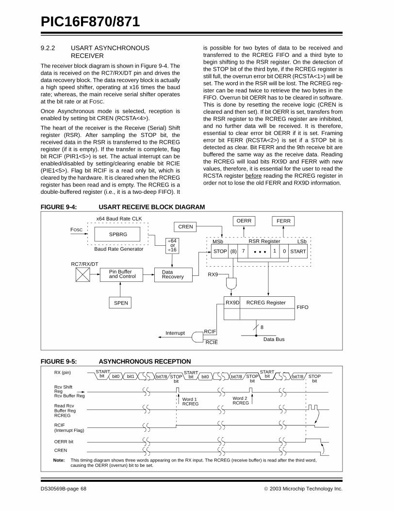
PIC16F870/871
9.2.2 USART ASYNCHRONOUS RECEIVER
The receiver block diagram is shown in Figure 9-4. Thedata is received on the RC7/RX/DT pin and drives thedata recovery block. The data recovery block is actuallya high speed shifter, operating at x16 times the baudrate; whereas, the main receive serial shifter operatesat the bit rate or at FOSC.
Once Asynchronous mode is selected, reception isenabled by setting bit CREN (RCSTA<4>).
The heart of the receiver is the Receive (Serial) Shiftregister (RSR). After sampling the STOP bit, thereceived data in the RSR is transferred to the RCREGregister (if it is empty). If the transfer is complete, flagbit RCIF (PIR1<5>) is set. The actual interrupt can beenabled/disabled by setting/clearing enable bit RCIE(PIE1<5>). Flag bit RCIF is a read only bit, which iscleared by the hardware. It is cleared when the RCREGregister has been read and is empty. The RCREG is adouble-buffered register (i.e., it is a two-deep FIFO). It
is possible for two bytes of data to be received andtransferred to the RCREG FIFO and a third byte tobegin shifting to the RSR register. On the detection ofthe STOP bit of the third byte, if the RCREG register isstill full, the overrun error bit OERR (RCSTA<1>) will beset. The word in the RSR will be lost. The RCREG reg-ister can be read twice to retrieve the two bytes in theFIFO. Overrun bit OERR has to be cleared in software.This is done by resetting the receive logic (CREN iscleared and then set). If bit OERR is set, transfers fromthe RSR register to the RCREG register are inhibited,and no further data will be received. It is therefore,essential to clear error bit OERR if it is set. Framingerror bit FERR (RCSTA<2>) is set if a STOP bit isdetected as clear. Bit FERR and the 9th receive bit arebuffered the same way as the receive data. Readingthe RCREG will load bits RX9D and FERR with newvalues, therefore, it is essential for the user to read theRCSTA register before reading the RCREG register inorder not to lose the old FERR and RX9D information.
FIGURE 9-4: USART RECEIVE BLOCK DIAGRAM
FIGURE 9-5: ASYNCHRONOUS RECEPTION
x64 Baud Rate CLK
SPBRG
Baud Rate Generator
RC7/RX/DT
Pin Bufferand Control
SPEN
DataRecovery
CRENOERR FERR
RSR RegisterMSb LSb
RX9D RCREG RegisterFIFO
Interrupt RCIF
RCIEData Bus
8
÷64
÷16or
STOP START(8) 7 1 0
RX9
• • •
FOSC
STARTbit bit7/8bit1bit0 bit7/8 bit0STOP
bit
STARTbit
STARTbitbit7/8 STOP
bit
RX (pin)
RegRcv Buffer Reg
Rcv Shift
Read RcvBuffer RegRCREG
RCIF(Interrupt Flag)
OERR bit
CREN
Word 1RCREG
Word 2RCREG
STOPbit
Note: This timing diagram shows three words appearing on the RX input. The RCREG (receive buffer) is read after the third word, causing the OERR (overrun) bit to be set.
DS30569B-page 68 2003 Microchip Technology Inc.
PIC16F870/871
When setting up an Asynchronous Reception, followthese steps:
1. Initialize the SPBRG register for the appropriatebaud rate. If a high speed baud rate is desired,set bit BRGH (Section 9.1).
2. Enable the asynchronous serial port by clearingbit SYNC and setting bit SPEN.
3. If interrupts are desired, then set enable bitRCIE.
4. If 9-bit reception is desired, then set bit RX9.
5. Enable the reception by setting bit CREN.
6. Flag bit RCIF will be set when reception is com-plete and an interrupt will be generated if enablebit RCIE is set.
7. Read the RCSTA register to get the ninth bit (ifenabled) and determine if any error occurredduring reception.
8. Read the 8-bit received data by reading theRCREG register.
9. If any error occurred, clear the error by clearingenable bit CREN.
10. If using interrupts, ensure that GIE and PEIE(bits 7 and 6) of the INTCON register are set.
TABLE 9-6: REGISTERS ASSOCIATED WITH ASYNCHRONOUS RECEPTION
Address Name Bit 7 Bit 6 Bit 5 Bit 4 Bit 3 Bit 2 Bit 1 Bit 0Value on:POR, BOR
Value onall otherRESETS
0Bh, 8Bh, 10Bh,18Bh
INTCON GIE PEIE T0IE INTE RBIE T0IF INTF R0IF 0000 000x 0000 000u
0Ch PIR1 PSPIF(1) ADIF RCIF TXIF — CCP1IF TMR2IF TMR1IF -000 0000 -000 0000
18h RCSTA SPEN RX9 SREN CREN — FERR OERR RX9D 0000 -00x 0000 -00x
1Ah RCREG USART Receive Register 0000 0000 0000 0000
8Ch PIE1 PSPIE(1) ADIE RCIE TXIE — CCP1IE TMR2IE TMR1IE 0000 -000 0000 -000
98h TXSTA CSRC TX9 TXEN SYNC — BRGH TRMT TX9D 0000 -010 0000 -010
99h SPBRG Baud Rate Generator Register 0000 0000 0000 0000
Legend: x = unknown, - = unimplemented locations read as '0'. Shaded cells are not used for asynchronous reception.Note 1: Bits PSPIE and PSPIF are reserved on the PIC16F870; always maintain these bits clear.
2003 Microchip Technology Inc. DS30569B-page 69
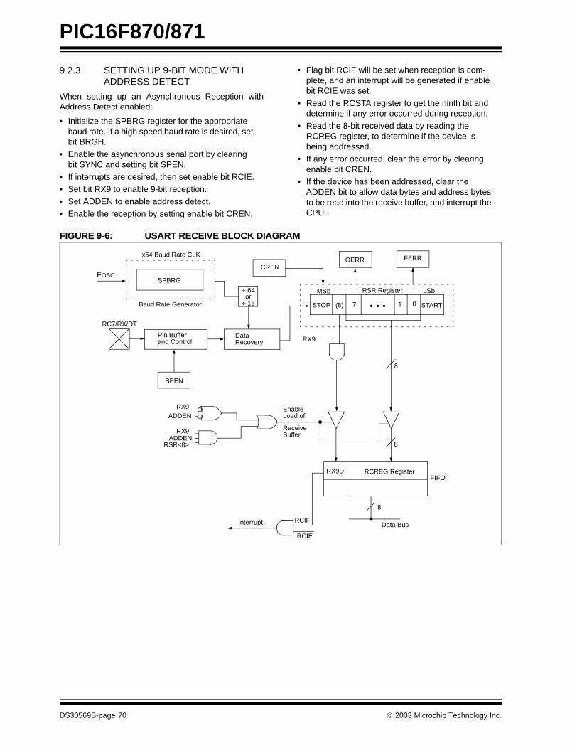
PIC16F870/871
9.2.3 SETTING UP 9-BIT MODE WITH ADDRESS DETECT
When setting up an Asynchronous Reception withAddress Detect enabled:
• Initialize the SPBRG register for the appropriate baud rate. If a high speed baud rate is desired, set bit BRGH.
• Enable the asynchronous serial port by clearing bit SYNC and setting bit SPEN.
• If interrupts are desired, then set enable bit RCIE.• Set bit RX9 to enable 9-bit reception.• Set ADDEN to enable address detect.
• Enable the reception by setting enable bit CREN.
• Flag bit RCIF will be set when reception is com-plete, and an interrupt will be generated if enable bit RCIE was set.
• Read the RCSTA register to get the ninth bit and determine if any error occurred during reception.
• Read the 8-bit received data by reading the RCREG register, to determine if the device is being addressed.
• If any error occurred, clear the error by clearing enable bit CREN.
• If the device has been addressed, clear the ADDEN bit to allow data bytes and address bytes to be read into the receive buffer, and interrupt the CPU.
FIGURE 9-6: USART RECEIVE BLOCK DIAGRAM
x64 Baud Rate CLK
SPBRG
Baud Rate Generator
RC7/RX/DT
Pin Bufferand Control
SPEN
DataRecovery
CRENOERR FERR
RSR RegisterMSb LSb
RX9D RCREG RegisterFIFO
Interrupt RCIF
RCIE
Data Bus
8
÷ 64
÷ 16or
STOP START(8) 7 1 0
RX9
• • •
RX9ADDEN
RX9ADDEN
RSR<8>
EnableLoad of
ReceiveBuffer
8
8
FOSC
DS30569B-page 70 2003 Microchip Technology Inc.
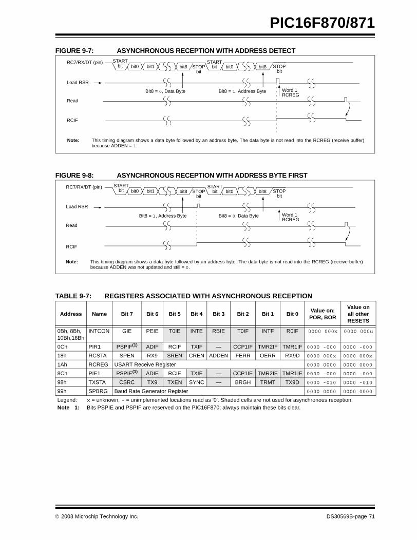
PIC16F870/871
FIGURE 9-7: ASYNCHRONOUS RECEPTION WITH ADDRESS DETECT
FIGURE 9-8: ASYNCHRONOUS RECEPTION WITH ADDRESS BYTE FIRST
TABLE 9-7: REGISTERS ASSOCIATED WITH ASYNCHRONOUS RECEPTION
STARTbit bit1bit0 bit8 bit0STOP
bit
STARTbit bit8 STOP
bit
RC7/RX/DT (pin)
Load RSR
Read
RCIF
Word 1RCREG
Bit8 = 0, Data Byte Bit8 = 1, Address Byte
Note: This timing diagram shows a data byte followed by an address byte. The data byte is not read into the RCREG (receive buffer)because ADDEN = 1.
STARTbit bit1bit0 bit8 bit0STOP
bit
STARTbit bit8 STOP
bit
RC7/RX/DT (pin)
Load RSR
Read
RCIF
Word 1RCREG
Bit8 = 1, Address Byte Bit8 = 0, Data Byte
Note: This timing diagram shows a data byte followed by an address byte. The data byte is not read into the RCREG (receive buffer)because ADDEN was not updated and still = 0.
Address Name Bit 7 Bit 6 Bit 5 Bit 4 Bit 3 Bit 2 Bit 1 Bit 0Value on:POR, BOR
Value onall otherRESETS
0Bh, 8Bh, 10Bh,18Bh
INTCON GIE PEIE T0IE INTE RBIE T0IF INTF R0IF 0000 000x 0000 000u
0Ch PIR1 PSPIF(1) ADIF RCIF TXIF — CCP1IF TMR2IF TMR1IF 0000 -000 0000 -000
18h RCSTA SPEN RX9 SREN CREN ADDEN FERR OERR RX9D 0000 000x 0000 000x
1Ah RCREG USART Receive Register 0000 0000 0000 0000
8Ch PIE1 PSPIE(1) ADIE RCIE TXIE — CCP1IE TMR2IE TMR1IE 0000 -000 0000 -000
98h TXSTA CSRC TX9 TXEN SYNC — BRGH TRMT TX9D 0000 -010 0000 -010
99h SPBRG Baud Rate Generator Register 0000 0000 0000 0000
Legend: x = unknown, - = unimplemented locations read as '0'. Shaded cells are not used for asynchronous reception.Note 1: Bits PSPIE and PSPIF are reserved on the PIC16F870; always maintain these bits clear.
2003 Microchip Technology Inc. DS30569B-page 71
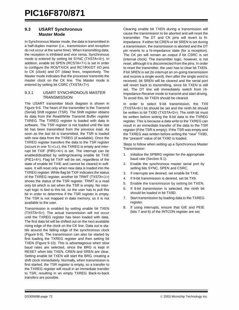
PIC16F870/871
9.3 USART Synchronous Master Mode
In Synchronous Master mode, the data is transmitted ina half-duplex manner (i.e., transmission and receptiondo not occur at the same time). When transmitting data,the reception is inhibited and vice versa. Synchronousmode is entered by setting bit SYNC (TXSTA<4>). Inaddition, enable bit SPEN (RCSTA<7>) is set in orderto configure the RC6/TX/CK and RC7/RX/DT I/O pinsto CK (clock) and DT (data) lines, respectively. TheMaster mode indicates that the processor transmits themaster clock on the CK line. The Master mode isentered by setting bit CSRC (TXSTA<7>).
9.3.1 USART SYNCHRONOUS MASTER TRANSMISSION
The USART transmitter block diagram is shown inFigure 9-6. The heart of the transmitter is the Transmit(Serial) Shift register (TSR). The Shift register obtainsits data from the Read/Write Transmit Buffer registerTXREG. The TXREG register is loaded with data insoftware. The TSR register is not loaded until the lastbit has been transmitted from the previous load. Assoon as the last bit is transmitted, the TSR is loadedwith new data from the TXREG (if available). Once theTXREG register transfers the data to the TSR register(occurs in one TCYCLE), the TXREG is empty and inter-rupt bit TXIF (PIR1<4>) is set. The interrupt can beenabled/disabled by setting/clearing enable bit TXIE(PIE1<4>). Flag bit TXIF will be set, regardless of thestate of enable bit TXIE and cannot be cleared in soft-ware. It will reset only when new data is loaded into theTXREG register. While flag bit TXIF indicates the statusof the TXREG register, another bit TRMT (TXSTA<1>)shows the status of the TSR register. TRMT is a readonly bit which is set when the TSR is empty. No inter-rupt logic is tied to this bit, so the user has to poll thisbit in order to determine if the TSR register is empty.The TSR is not mapped in data memory, so it is notavailable to the user.
Transmission is enabled by setting enable bit TXEN(TXSTA<5>). The actual transmission will not occuruntil the TXREG register has been loaded with data.The first data bit will be shifted out on the next availablerising edge of the clock on the CK line. Data out is sta-ble around the falling edge of the synchronous clock(Figure 9-9). The transmission can also be started byfirst loading the TXREG register and then setting bitTXEN (Figure 9-10). This is advantageous when slowbaud rates are selected, since the BRG is kept inRESET when bits TXEN, CREN and SREN are clear.Setting enable bit TXEN will start the BRG, creating ashift clock immediately. Normally, when transmission isfirst started, the TSR register is empty, so a transfer tothe TXREG register will result in an immediate transferto TSR, resulting in an empty TXREG. Back-to-backtransfers are possible.
Clearing enable bit TXEN during a transmission willcause the transmission to be aborted and will reset thetransmitter. The DT and CK pins will revert to hi-impedance. If either bit CREN or bit SREN is set duringa transmission, the transmission is aborted and the DTpin reverts to a hi-impedance state (for a reception).The CK pin will remain an output if bit CSRC is set(internal clock). The transmitter logic, however, is notreset, although it is disconnected from the pins. In orderto reset the transmitter, the user has to clear bit TXEN.If bit SREN is set (to interrupt an on-going transmissionand receive a single word), then after the single word isreceived, bit SREN will be cleared and the serial portwill revert back to transmitting, since bit TXEN is stillset. The DT line will immediately switch from Hi-Impedance Receive mode to transmit and start driving.To avoid this, bit TXEN should be cleared.
In order to select 9-bit transmission, the TX9(TXSTA<6>) bit should be set and the ninth bit shouldbe written to bit TX9D (TXSTA<0>). The ninth bit mustbe written before writing the 8-bit data to the TXREGregister. This is because a data write to the TXREG canresult in an immediate transfer of the data to the TSRregister (if the TSR is empty). If the TSR was empty andthe TXREG was written before writing the “new” TX9D,the “present” value of bit TX9D is loaded.
Steps to follow when setting up a Synchronous MasterTransmission:
1. Initialize the SPBRG register for the appropriatebaud rate (Section 9.1).
2. Enable the synchronous master serial port bysetting bits SYNC, SPEN and CSRC.
3. If interrupts are desired, set enable bit TXIE.4. If 9-bit transmission is desired, set bit TX9.5. Enable the transmission by setting bit TXEN.
6. If 9-bit transmission is selected, the ninth bitshould be loaded in bit TX9D.
7. Start transmission by loading data to the TXREGregister.
8. If using interrupts, ensure that GIE and PEIE(bits 7 and 6) of the INTCON register are set.
DS30569B-page 72 2003 Microchip Technology Inc.

PIC16F870/871
TABLE 9-8: REGISTERS ASSOCIATED WITH SYNCHRONOUS MASTER TRANSMISSION
FIGURE 9-9: SYNCHRONOUS TRANSMISSION
FIGURE 9-10: SYNCHRONOUS TRANSMISSION (THROUGH TXEN)
Address Name Bit 7 Bit 6 Bit 5 Bit 4 Bit 3 Bit 2 Bit 1 Bit 0Value on: POR, BOR
Value on all other RESETS
0Bh, 8Bh, 10Bh,18Bh
INTCON GIE PEIE T0IE INTE RBIE T0IF INTF R0IF 0000 000x 0000 000u
0Ch PIR1 PSPIF(1) ADIF RCIF TXIF — CCP1IF TMR2IF TMR1IF 0000 -000 0000 -000
18h RCSTA SPEN RX9 SREN CREN — FERR OERR RX9D 0000 -00x 0000 -00x
19h TXREG USART Transmit Register 0000 0000 0000 0000
8Ch PIE1 PSPIE(1) ADIE RCIE TXIE — CCP1IE TMR2IE TMR1IE 0000 -000 0000 -000
98h TXSTA CSRC TX9 TXEN SYNC — BRGH TRMT TX9D 0000 -010 0000 -010
99h SPBRG Baud Rate Generator Register 0000 0000 0000 0000
Legend: x = unknown, - = unimplemented, read as '0'. Shaded cells are not used for synchronous master transmission.Note 1: Bits PSPIE and PSPIF are reserved on the PIC16F870; always maintain these bits clear.
bit 0 bit 1 bit 7
Word 1
Q1Q2 Q3Q4 Q1 Q2Q3 Q4Q1 Q2Q3 Q4Q1 Q2Q3 Q4Q1 Q2 Q3Q4 Q3Q4 Q1Q2 Q3Q4 Q1Q2 Q3Q4 Q1Q2 Q3 Q4Q1 Q2Q3 Q4Q1 Q2Q3 Q4Q1 Q2Q3 Q4
bit 2 bit 0 bit 1 bit 7RC7/RX/DT pin
RC6/TX/CK pin
Write toTXREG reg
TXIF bit(Interrupt Flag)
TXEN bit'1' '1'
Word 2
TRMT bit
Write Word1 Write Word2
Note: Sync Master mode; SPBRG = 0. Continuous transmission of two 8-bit words.
RC7/RX/DT pin
RC6/TX/CK pin
Write toTXREG Reg
TXIF bit
TRMT bit
bit0 bit1 bit2 bit6 bit7
TXEN bit
2003 Microchip Technology Inc. DS30569B-page 73
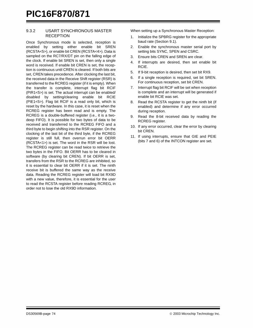
PIC16F870/871
9.3.2 USART SYNCHRONOUS MASTER RECEPTION
Once Synchronous mode is selected, reception isenabled by setting either enable bit SREN(RCSTA<5>), or enable bit CREN (RCSTA<4>). Data issampled on the RC7/RX/DT pin on the falling edge ofthe clock. If enable bit SREN is set, then only a singleword is received. If enable bit CREN is set, the recep-tion is continuous until CREN is cleared. If both bits areset, CREN takes precedence. After clocking the last bit,the received data in the Receive Shift register (RSR) istransferred to the RCREG register (if it is empty). Whenthe transfer is complete, interrupt flag bit RCIF(PIR1<5>) is set. The actual interrupt can be enabled/disabled by setting/clearing enable bit RCIE(PIE1<5>). Flag bit RCIF is a read only bit, which isreset by the hardware. In this case, it is reset when theRCREG register has been read and is empty. TheRCREG is a double-buffered register (i.e., it is a two-deep FIFO). It is possible for two bytes of data to bereceived and transferred to the RCREG FIFO and athird byte to begin shifting into the RSR register. On theclocking of the last bit of the third byte, if the RCREGregister is still full, then overrun error bit OERR(RCSTA<1>) is set. The word in the RSR will be lost.The RCREG register can be read twice to retrieve thetwo bytes in the FIFO. Bit OERR has to be cleared insoftware (by clearing bit CREN). If bit OERR is set,transfers from the RSR to the RCREG are inhibited, soit is essential to clear bit OERR if it is set. The ninthreceive bit is buffered the same way as the receivedata. Reading the RCREG register will load bit RX9Dwith a new value, therefore, it is essential for the userto read the RCSTA register before reading RCREG, inorder not to lose the old RX9D information.
When setting up a Synchronous Master Reception:
1. Initialize the SPBRG register for the appropriatebaud rate (Section 9.1).
2. Enable the synchronous master serial port bysetting bits SYNC, SPEN and CSRC.
3. Ensure bits CREN and SREN are clear.4. If interrupts are desired, then set enable bit
RCIE.5. If 9-bit reception is desired, then set bit RX9.
6. If a single reception is required, set bit SREN.For continuous reception, set bit CREN.
7. Interrupt flag bit RCIF will be set when receptionis complete and an interrupt will be generated ifenable bit RCIE was set.
8. Read the RCSTA register to get the ninth bit (ifenabled) and determine if any error occurredduring reception.
9. Read the 8-bit received data by reading theRCREG register.
10. If any error occurred, clear the error by clearingbit CREN.
11. If using interrupts, ensure that GIE and PEIE(bits 7 and 6) of the INTCON register are set.
DS30569B-page 74 2003 Microchip Technology Inc.
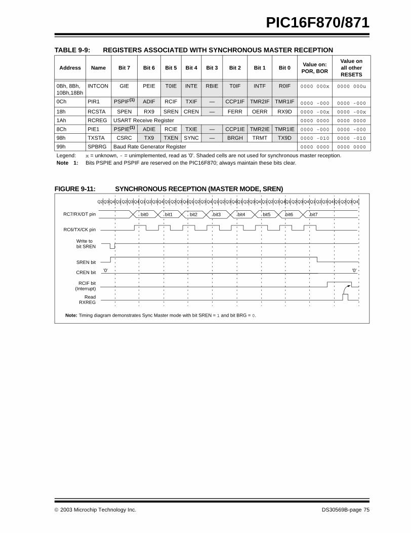
PIC16F870/871
TABLE 9-9: REGISTERS ASSOCIATED WITH SYNCHRONOUS MASTER RECEPTION
FIGURE 9-11: SYNCHRONOUS RECEPTION (MASTER MODE, SREN)
Address Name Bit 7 Bit 6 Bit 5 Bit 4 Bit 3 Bit 2 Bit 1 Bit 0Value on: POR, BOR
Value on all other RESETS
0Bh, 8Bh, 10Bh,18Bh
INTCON GIE PEIE T0IE INTE RBIE T0IF INTF R0IF 0000 000x 0000 000u
0Ch PIR1 PSPIF(1) ADIF RCIF TXIF — CCP1IF TMR2IF TMR1IF 0000 -000 0000 -000
18h RCSTA SPEN RX9 SREN CREN — FERR OERR RX9D 0000 -00x 0000 -00x
1Ah RCREG USART Receive Register 0000 0000 0000 0000
8Ch PIE1 PSPIE(1) ADIE RCIE TXIE — CCP1IE TMR2IE TMR1IE 0000 -000 0000 -000
98h TXSTA CSRC TX9 TXEN SYNC — BRGH TRMT TX9D 0000 -010 0000 -010
99h SPBRG Baud Rate Generator Register 0000 0000 0000 0000
Legend: x = unknown, - = unimplemented, read as '0'. Shaded cells are not used for synchronous master reception.Note 1: Bits PSPIE and PSPIF are reserved on the PIC16F870; always maintain these bits clear.
CREN bit
RC7/RX/DT pin
RC6/TX/CK pin
Write tobit SREN
SREN bit
RCIF bit(Interrupt)
ReadRXREG
Note: Timing diagram demonstrates Sync Master mode with bit SREN = 1 and bit BRG = 0.
Q3 Q4 Q1 Q2 Q3 Q4 Q1 Q2 Q3 Q4Q2 Q1 Q2 Q3 Q4Q1 Q2 Q3 Q4 Q1 Q2 Q3 Q4Q1 Q2 Q3 Q4 Q1 Q2 Q3 Q4Q1 Q2 Q3 Q4 Q1 Q2 Q3 Q4
'0'
bit0 bit1 bit2 bit3 bit4 bit5 bit6 bit7
'0'
Q1 Q2 Q3 Q4
2003 Microchip Technology Inc. DS30569B-page 75
PIC16F870/871
9.4 USART Synchronous Slave Mode
Synchronous Slave mode differs from the Master modein the fact that the shift clock is supplied externally atthe RC6/TX/CK pin (instead of being supplied internallyin Master mode). This allows the device to transfer orreceive data while in SLEEP mode. Slave mode isentered by clearing bit CSRC (TXSTA<7>).
9.4.1 USART SYNCHRONOUS SLAVE TRANSMIT
The operation of the Synchronous Master and Slavemodes is identical, except in the case of the SLEEP mode.
If two words are written to the TXREG and then theSLEEP instruction is executed, the following will occur:
a) The first word will immediately transfer to theTSR register and transmit.
b) The second word will remain in TXREG register. c) Flag bit TXIF will not be set.
d) When the first word has been shifted out of TSR,the TXREG register will transfer the second wordto the TSR and flag bit TXIF will now be set.
e) If enable bit TXIE is set, the interrupt will wakethe chip from SLEEP and if the global interruptis enabled, the program will branch to theinterrupt vector (0004h).
When setting up a Synchronous Slave Transmission,follow these steps:
1. Enable the synchronous slave serial port by set-ting bits SYNC and SPEN and clearing bitCSRC.
2. Clear bits CREN and SREN.
3. If interrupts are desired, then set enable bitTXIE.
4. If 9-bit transmission is desired, then set bit TX9.5. Enable the transmission by setting enable bit
TXEN.6. If 9-bit transmission is selected, the ninth bit
should be loaded in bit TX9D.7. Start transmission by loading data to the TXREG
register.8. If using interrupts, ensure that GIE and PEIE
(bits 7 and 6) of the INTCON register are set.
TABLE 9-10: REGISTERS ASSOCIATED WITH SYNCHRONOUS SLAVE TRANSMISSION
Address Name Bit 7 Bit 6 Bit 5 Bit 4 Bit 3 Bit 2 Bit 1 Bit 0Value on: POR, BOR
Value on all other RESETS
0Bh, 8Bh, 10Bh,18Bh
INTCON GIE PEIE T0IE INTE RBIE T0IF INTF R0IF 0000 000x 0000 000u
0Ch PIR1 PSPIF(1) ADIF RCIF TXIF — CCP1IF TMR2IF TMR1IF 0000 -000 0000 -000
18h RCSTA SPEN RX9 SREN CREN ADDEN FERR OERR RX9D 0000 000x 0000 000x
19h TXREG USART Transmit Register 0000 0000 0000 0000
8Ch PIE1 PSPIE(1) ADIE RCIE TXIE — CCP1IE TMR2IE TMR1IE 0000 -000 0000 -000
98h TXSTA CSRC TX9 TXEN SYNC — BRGH TRMT TX9D 0000 -010 0000 -010
99h SPBRG Baud Rate Generator Register 0000 0000 0000 0000
Legend: x = unknown, - = unimplemented, read as '0'. Shaded cells are not used for synchronous slave transmission.Note 1: Bits PSPIE and PSPIF are reserved on the PIC16F870; always maintain these bits clear.
DS30569B-page 76 2003 Microchip Technology Inc.
PIC16F870/871
9.4.2 USART SYNCHRONOUS SLAVE RECEPTION
The operation of the Synchronous Master and Slavemodes is identical, except in the case of the SLEEPmode. Bit SREN is a “don't care” in Slave mode.
If receive is enabled by setting bit CREN prior to theSLEEP instruction, then a word may be received duringSLEEP. On completely receiving the word, the RSRregister will transfer the data to the RCREG registerand if enable bit RCIE bit is set, the interrupt generatedwill wake the chip from SLEEP. If the global interrupt isenabled, the program will branch to the interrupt vector(0004h).
When setting up a Synchronous Slave Reception,follow these steps:
1. Enable the synchronous master serial port bysetting bits SYNC and SPEN and clearing bitCSRC.
2. If interrupts are desired, set enable bit RCIE.
3. If 9-bit reception is desired, set bit RX9.4. To enable reception, set enable bit CREN.5. Flag bit RCIF will be set when reception is com-
plete and an interrupt will be generated, ifenable bit RCIE was set.
6. Read the RCSTA register to get the ninth bit (ifenabled) and determine if any error occurredduring reception.
7. Read the 8-bit received data by reading theRCREG register.
8. If any error occurred, clear the error by clearingbit CREN.
9. If using interrupts, ensure that GIE and PEIE(bits 7 and 6) of the INTCON register are set.
TABLE 9-11: REGISTERS ASSOCIATED WITH SYNCHRONOUS SLAVE RECEPTION
Address Name Bit 7 Bit 6 Bit 5 Bit 4 Bit 3 Bit 2 Bit 1 Bit 0Value on: POR, BOR
Value on all other RESETS
0Bh, 8Bh, 10Bh,18Bh
INTCON GIE PEIE T0IE INTE RBIE T0IF INTF R0IF 0000 000x 0000 000u
0Ch PIR1 PSPIF(1) ADIF RCIF TXIF — CCP1IF TMR2IF TMR1IF 0000 -000 0000 -000
18h RCSTA SPEN RX9 SREN CREN ADDEN FERR OERR RX9D 0000 000x 0000 000x
1Ah RCREG USART Receive Register 0000 0000 0000 0000
8Ch PIE1 PSPIE(1) ADIE RCIE TXIE — CCP1IE TMR2IE TMR1IE 0000 -000 0000 -000
98h TXSTA CSRC TX9 TXEN SYNC — BRGH TRMT TX9D 0000 -010 0000 -010
99h SPBRG Baud Rate Generator Register 0000 0000 0000 0000
Legend: x = unknown, - = unimplemented, read as '0'. Shaded cells are not used for synchronous slave reception.Note 1: Bits PSPIE and PSPIF are reserved on the PIC16F870, always maintain these bits clear.
2003 Microchip Technology Inc. DS30569B-page 77

PIC16F870/871
NOTES:
DS30569B-page 78 2003 Microchip Technology Inc.
PIC16F870/871
10.0 ANALOG-TO-DIGITAL (A/D) CONVERTER MODULE
The Analog-to-Digital (A/D) Converter module has fiveinputs for the 28-pin devices and eight for the otherdevices.
The analog input charges a sample and hold capacitor.The output of the sample and hold capacitor is the inputinto the converter. The converter then generates a dig-ital result of this analog level via successive approxima-tion. The A/D conversion of the analog input signalresults in a corresponding 10-bit digital number. TheA/D module has high and low voltage reference inputthat is software selectable to some combination of VDD,VSS, RA2, or RA3.
The A/D converter has a unique feature of being ableto operate while the device is in SLEEP mode. To oper-ate in SLEEP, the A/D clock must be derived from theA/D’s internal RC oscillator.
The A/D module has four registers. These registersare:
• A/D Result High Register (ADRESH)• A/D Result Low Register (ADRESL)• A/D Control Register0 (ADCON0)
• A/D Control Register1 (ADCON1)
The ADCON0 register, shown in Register 10-1, con-trols the operation of the A/D module. The ADCON1register, shown in Register 10-2, configures the func-tions of the port pins. The port pins can be configuredas analog inputs (RA3 can also be the voltagereference), or as digital I/O.
Additional information on using the A/D module can befound in the PICmicro™ Mid-Range MCU FamilyReference Manual (DS33023).
REGISTER 10-1: ADCON0 REGISTER (ADDRESS: 1Fh) R/W-0 R/W-0 R/W-0 R/W-0 R/W-0 R/W-0 U-0 R/W-0
ADCS1 ADCS0 CHS2 CHS1 CHS0 GO/DONE — ADON
bit 7 bit 0
bit 7-6 ADCS1:ADCS0: A/D Conversion Clock Select bits
00 = FOSC/201 = FOSC/810 = FOSC/3211 = FRC (clock derived from the internal A/D module RC oscillator)
bit 5-3 CHS2:CHS0: Analog Channel Select bits
000 = Channel 0, (RA0/AN0)010 = Channel 2, (RA2/AN2)011 = Channel 3, (RA3/AN3)100 = Channel 4, (RA5/AN4)101 = Channel 5, (RE0/AN5)(1)
110 = Channel 6, (RE1/AN6)(1)
111 = Channel 7, (RE2/AN7)(1)
bit 2 GO/DONE: A/D Conversion Status bit
If ADON = 1:1 = A/D conversion in progress (setting this bit starts the A/D conversion)0 = A/D conversion not in progress (this bit is automatically cleared by hardware when the A/D
conversion is complete)
bit 1 Unimplemented: Read as '0'
bit 0 ADON: A/D On bit1 = A/D converter module is operating0 = A/D converter module is shut-off and consumes no operating current
Note 1: These channels are not available on the PIC16F870 device.
Legend:
R = Readable bit W = Writable bit U = Unimplemented bit, read as ‘0’
- n = Value at POR ‘1’ = Bit is set ‘0’ = Bit is cleared x = Bit is unknown
2003 Microchip Technology Inc. DS30569B-page 79
PIC16F870/871
REGISTER 10-2: ADCON1 REGISTER (ADDRESS: 9Fh)
The ADRESH:ADRESL registers contain the 10-bitresult of the A/D conversion. When the A/D conversionis complete, the result is loaded into this A/D result reg-ister pair, the GO/DONE bit (ADCON0<2>) is clearedand the A/D interrupt flag bit ADIF is set. The blockdiagram of the A/D module is shown in Figure 10-1.
After the A/D module has been configured as desired,the selected channel must be acquired before the con-version is started. The analog input channels musthave their corresponding TRIS bits selected as inputs.
To determine sample time, see Section 10.1. After thisacquisition time has elapsed, the A/D conversion canbe started.
U-0 U-0 R/W-0 U-0 R/W-0 R/W-0 R/W-0 R/W-0
ADFM — — — PCFG3 PCFG2 PCFG1 PCFG0
bit 7 bit 0
bit 7 ADFM: A/D Result Format Select bit1 = Right justified. 6 Most Significant bits of ADRESH are read as ‘0’.0 = Left justified. 6 Least Significant bits of ADRESL are read as ‘0’.
bit 6-4 Unimplemented: Read as '0'
bit 3-0 PCFG3:PCFG0: A/D Port Configuration Control bits:
Note 1: These channels are not available on the PIC16F870 device.
2: This column indicates the number of analog channels available as A/D inputs andthe number of analog channels used as voltage reference inputs.
Legend:
R = Readable bit W = Writable bit U = Unimplemented bit, read as ‘0’
- n = Value at POR ‘1’ = Bit is set ‘0’ = Bit is cleared x = Bit is unknown
A = Analog input D = Digital I/O
PCFG3:PCFG0
AN7(1)
RE2AN6(1)
RE1AN5(1)
RE0AN4RA5
AN3RA3
AN2RA2
AN1RA1
AN0RA0
VREF+ VREF-CHAN/Refs(2)
0000 A A A A A A A A VDD VSS 8/0
0001 A A A A VREF+ A A A RA3 VSS 7/1
0010 D D D A A A A A VDD VSS 5/0
0011 D D D A VREF+ A A A RA3 VSS 4/1
0100 D D D D A D A A VDD VSS 3/0
0101 D D D D VREF+ D A A RA3 VSS 2/1
011x D D D D D D D D VDD VSS 0/0
1000 A A A A VREF+ VREF- A A RA3 RA2 6/2
1001 D D A A A A A A VDD VSS 6/0
1010 D D A A VREF+ A A A RA3 VSS 5/1
1011 D D A A VREF+ VREF- A A RA3 RA2 4/2
1100 D D D A VREF+ VREF- A A RA3 RA2 3/2
1101 D D D D VREF+ VREF- A A RA3 RA2 2/2
1110 D D D D D D D A VDD VSS 1/0
1111 D D D D VREF+ VREF- D A RA3 RA2 1/2
DS30569B-page 80 2003 Microchip Technology Inc.
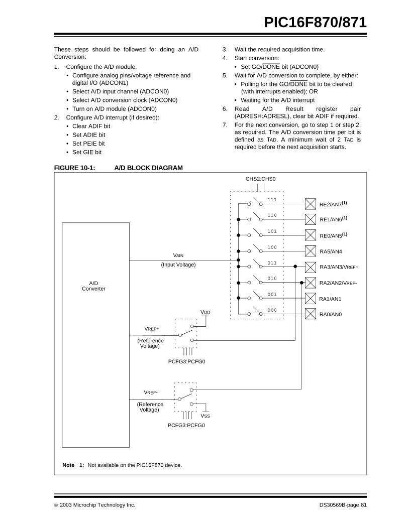
PIC16F870/871
These steps should be followed for doing an A/DConversion:
1. Configure the A/D module:• Configure analog pins/voltage reference and
digital I/O (ADCON1)• Select A/D input channel (ADCON0)• Select A/D conversion clock (ADCON0)
• Turn on A/D module (ADCON0)2. Configure A/D interrupt (if desired):
• Clear ADIF bit
• Set ADIE bit• Set PEIE bit • Set GIE bit
3. Wait the required acquisition time.4. Start conversion:
• Set GO/DONE bit (ADCON0)5. Wait for A/D conversion to complete, by either:
• Polling for the GO/DONE bit to be cleared (with interrupts enabled); OR
• Waiting for the A/D interrupt
6. Read A/D Result register pair(ADRESH:ADRESL), clear bit ADIF if required.
7. For the next conversion, go to step 1 or step 2,as required. The A/D conversion time per bit isdefined as TAD. A minimum wait of 2 TAD isrequired before the next acquisition starts.
FIGURE 10-1: A/D BLOCK DIAGRAM
(Input Voltage)
VAIN
VREF+
(ReferenceVoltage)
VDD
PCFG3:PCFG0
CHS2:CHS0
RE2/AN7(1)
RE1/AN6(1)
RE0/AN5(1)
RA5/AN4
RA3/AN3/VREF+
RA2/AN2/VREF-
RA1/AN1
RA0/AN0
111
110
101
100
011
010
001
000
A/DConverter
Note 1: Not available on the PIC16F870 device.
VREF-
(ReferenceVoltage)
VSS
PCFG3:PCFG0
2003 Microchip Technology Inc. DS30569B-page 81
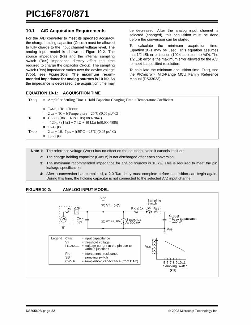
PIC16F870/871
10.1 A/D Acquisition Requirements
For the A/D converter to meet its specified accuracy,the charge holding capacitor (CHOLD) must be allowedto fully charge to the input channel voltage level. Theanalog input model is shown in Figure 10-2. Thesource impedance (RS) and the internal samplingswitch (RSS) impedance directly affect the timerequired to charge the capacitor CHOLD. The samplingswitch (RSS) impedance varies over the device voltage(VDD), see Figure 10-2. The maximum recom-mended impedance for analog sources is 10 kΩ. Asthe impedance is decreased, the acquisition time may
be decreased. After the analog input channel isselected (changed), this acquisition must be donebefore the conversion can be started.
To calculate the minimum acquisition time,Equation 10-1 may be used. This equation assumesthat 1/2 LSb error is used (1024 steps for the A/D). The1/2 LSb error is the maximum error allowed for the A/Dto meet its specified resolution.
To calculate the minimum acquisition time, TACQ, seethe PICmicro™ Mid-Range MCU Family ReferenceManual (DS33023).
EQUATION 10-1: ACQUISITION TIME
FIGURE 10-2: ANALOG INPUT MODEL
TACQ
TC
TACQ
=
=======
Amplifier Settling Time + Hold Capacitor Charging Time + Temperature Coefficient
TAMP + TC + TCOFF
2 µs + TC + [(Temperature – 25°C)(0.05 µs/°C)] CHOLD (RIC + RSS + RS) In(1/2047)- 120 pF (1 kΩ + 7 kΩ + 10 kΩ) In(0.0004885)16.47 µs2 µs + 16.47 µs + [(50°C – 25°C)(0.05 µs/°C)19.72 µs
Note 1: The reference voltage (VREF) has no effect on the equation, since it cancels itself out.
2: The charge holding capacitor (CHOLD) is not discharged after each conversion.
3: The maximum recommended impedance for analog sources is 10 kΩ. This is required to meet the pinleakage specification.
4: After a conversion has completed, a 2.0 TAD delay must complete before acquisition can begin again.During this time, the holding capacitor is not connected to the selected A/D input channel.
CPINVA
RS ANx
5 pF
VDD
VT = 0.6V
VT = 0.6V I LEAKAGE
RIC ≤ 1k
SamplingSwitchSS RSS
CHOLD= DAC capacitance
VSS
6V
Sampling Switch
5V4V3V2V
5 6 7 8 9 10 11
(kΩ)
VDD
= 120 pF± 500 nA
Legend CPIN
VTI LEAKAGE
RICSSCHOLD
= input capacitance= threshold voltage= leakage current at the pin due to
= interconnect resistance= sampling switch= sample/hold capacitance (from DAC)
various junctions
DS30569B-page 82 2003 Microchip Technology Inc.
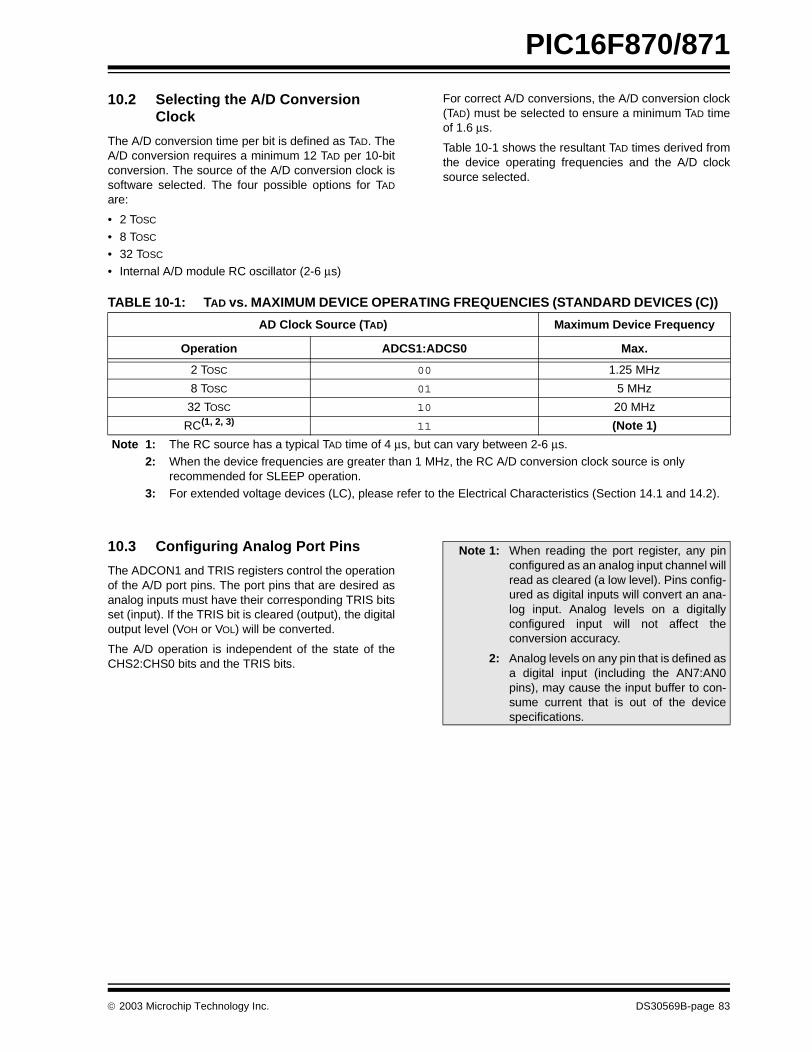
PIC16F870/871
10.2 Selecting the A/D Conversion Clock
The A/D conversion time per bit is defined as TAD. TheA/D conversion requires a minimum 12 TAD per 10-bitconversion. The source of the A/D conversion clock issoftware selected. The four possible options for TAD
are:
• 2 TOSC
• 8 TOSC
• 32 TOSC
• Internal A/D module RC oscillator (2-6 µs)
For correct A/D conversions, the A/D conversion clock(TAD) must be selected to ensure a minimum TAD timeof 1.6 µs.
Table 10-1 shows the resultant TAD times derived fromthe device operating frequencies and the A/D clocksource selected.
TABLE 10-1: TAD vs. MAXIMUM DEVICE OPERATING FREQUENCIES (STANDARD DEVICES (C))
10.3 Configuring Analog Port Pins
The ADCON1 and TRIS registers control the operationof the A/D port pins. The port pins that are desired asanalog inputs must have their corresponding TRIS bitsset (input). If the TRIS bit is cleared (output), the digitaloutput level (VOH or VOL) will be converted.
The A/D operation is independent of the state of theCHS2:CHS0 bits and the TRIS bits.
AD Clock Source (TAD) Maximum Device Frequency
Operation ADCS1:ADCS0 Max.
2 TOSC 00 1.25 MHz
8 TOSC 01 5 MHz
32 TOSC 10 20 MHz
RC(1, 2, 3) 11 (Note 1)
Note 1: The RC source has a typical TAD time of 4 µs, but can vary between 2-6 µs.2: When the device frequencies are greater than 1 MHz, the RC A/D conversion clock source is only
recommended for SLEEP operation. 3: For extended voltage devices (LC), please refer to the Electrical Characteristics (Section 14.1 and 14.2).
Note 1: When reading the port register, any pinconfigured as an analog input channel willread as cleared (a low level). Pins config-ured as digital inputs will convert an ana-log input. Analog levels on a digitallyconfigured input will not affect theconversion accuracy.
2: Analog levels on any pin that is defined asa digital input (including the AN7:AN0pins), may cause the input buffer to con-sume current that is out of the devicespecifications.
2003 Microchip Technology Inc. DS30569B-page 83
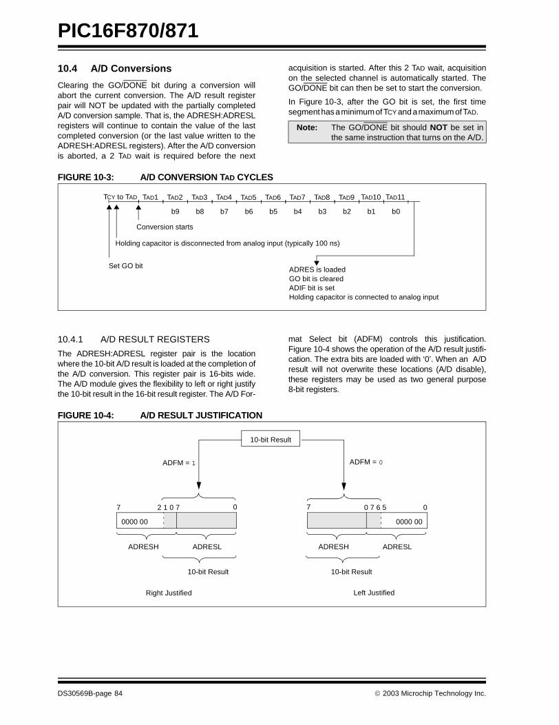
PIC16F870/871
10.4 A/D Conversions
Clearing the GO/DONE bit during a conversion willabort the current conversion. The A/D result registerpair will NOT be updated with the partially completedA/D conversion sample. That is, the ADRESH:ADRESLregisters will continue to contain the value of the lastcompleted conversion (or the last value written to theADRESH:ADRESL registers). After the A/D conversionis aborted, a 2 TAD wait is required before the next
acquisition is started. After this 2 TAD wait, acquisitionon the selected channel is automatically started. TheGO/DONE bit can then be set to start the conversion.
In Figure 10-3, after the GO bit is set, the first timesegment has a minimum of TCY and a maximum of TAD.
FIGURE 10-3: A/D CONVERSION TAD CYCLES
10.4.1 A/D RESULT REGISTERS
The ADRESH:ADRESL register pair is the locationwhere the 10-bit A/D result is loaded at the completion ofthe A/D conversion. This register pair is 16-bits wide.The A/D module gives the flexibility to left or right justifythe 10-bit result in the 16-bit result register. The A/D For-
mat Select bit (ADFM) controls this justification.Figure 10-4 shows the operation of the A/D result justifi-cation. The extra bits are loaded with ‘0’. When an A/Dresult will not overwrite these locations (A/D disable),these registers may be used as two general purpose8-bit registers.
FIGURE 10-4: A/D RESULT JUSTIFICATION
Note: The GO/DONE bit should NOT be set inthe same instruction that turns on the A/D.
TAD1 TAD2 TAD3 TAD4 TAD5 TAD6 TAD7 TAD8 TAD9
Set GO bit
Holding capacitor is disconnected from analog input (typically 100 ns)
b9 b8 b7 b6 b5 b4 b3 b2
TAD10 TAD11
b1 b0
TCY to TAD
Conversion starts
ADRES is loadedGO bit is clearedADIF bit is setHolding capacitor is connected to analog input
10-bit Result
ADRESH ADRESL
0000 00
ADFM = 0
02 1 0 77
10-bit Result
ADRESH ADRESL
10-bit Result
0000 00
7 0 7 6 5 0
ADFM = 1
Right Justified Left Justified
DS30569B-page 84 2003 Microchip Technology Inc.

PIC16F870/871
10.5 A/D Operation During SLEEP
The A/D module can operate during SLEEP mode. Thisrequires that the A/D clock source be set to RC(ADCS1:ADCS0 = 11). When the RC clock source isselected, the A/D module waits one instruction cyclebefore starting the conversion. This allows the SLEEPinstruction to be executed, which eliminates all digitalswitching noise from the conversion. When the conver-sion is completed, the GO/DONE bit will be cleared andthe result loaded into the ADRES register. If the A/Dinterrupt is enabled, the device will wake-up fromSLEEP. If the A/D interrupt is not enabled, the A/D mod-ule will then be turned off, although the ADON bit willremain set.
When the A/D clock source is another clock option (notRC), a SLEEP instruction will cause the present conver-sion to be aborted and the A/D module to be turned off,though the ADON bit will remain set.
Turning off the A/D places the A/D module in its lowestcurrent consumption state.
10.6 Effects of a RESET
A device RESET forces all registers to their RESETstate. This forces the A/D module to be turned off, andany conversion is aborted. All A/D input pins areconfigured as analog inputs.
The value that is in the ADRESH:ADRESL registers isnot modified for a Power-on Reset. TheADRESH:ADRESL registers will contain unknown dataafter a Power-on Reset.
TABLE 10-2: REGISTERS/BITS ASSOCIATED WITH A/D
Note: For the A/D module to operate in SLEEP,the A/D clock source must be set to RC(ADCS1:ADCS0 = 11). To allow the con-version to occur during SLEEP, ensure theSLEEP instruction immediately follows theinstruction that sets the GO/DONE bit.
Address Name Bit 7 Bit 6 Bit 5 Bit 4 Bit 3 Bit 2 Bit 1 Bit 0Value on
POR, BOR
Value on MCLR,WDT
0Bh,8Bh,10Bh,18Bh
INTCON GIE PEIE T0IE INTE RBIE T0IF INTF RBIF 0000 000x 0000 000u
0Ch PIR1 PSPIF(1) ADIF RCIF TXIF — CCP1IF TMR2IF TMR1IF 0000 -000 0000 -000
8Ch PIE1 PSPIE(1) ADIE RCIE TXIE — CCP1IE TMR2IE TMR1IE 0000 -000 0000 -000
1Eh ADRESH A/D Result Register High Byte xxxx xxxx uuuu uuuu
9Eh ADRESL A/D Result Register Low Byte xxxx xxxx uuuu uuuu
1Fh ADCON0 ADCS1 ADCS0 CHS2 CHS1 CHS0 GO/DONE — ADON 0000 00-0 0000 00-0
9Fh ADCON1 ADFM — — — PCFG3 PCFG2 PCFG1 PCFG0 --0- 0000 --0- 0000
85h TRISA — — PORTA Data Direction Register --11 1111 --11 1111
05h PORTA — — PORTA Data Latch when written: PORTA pins when read --0x 0000 --0u 0000
89h(1) TRISE IBF OBF IBOV PSPMODE — PORTE Data Direction bits 0000 -111 0000 -111
09h(1) PORTE — — — — — RE2 RE1 RE0 ---- -xxx ---- -uuu
Legend: x = unknown, u = unchanged, - = unimplemented, read as '0'. Shaded cells are not used for A/D conversion.Note 1: These registers/bits are not available on the 28-pin devices.
2003 Microchip Technology Inc. DS30569B-page 85

PIC16F870/871
NOTES:
DS30569B-page 86 2003 Microchip Technology Inc.
PIC16F870/871
11.0 SPECIAL FEATURES OF THE CPU
The PIC16F870/871 devices have a host of featuresintended to maximize system reliability, minimize costthrough elimination of external components, providePower Saving Operating modes and offer codeprotection. These are:
• Oscillator Selection• RESET
- Power-on Reset (POR)- Power-up Timer (PWRT)- Oscillator Start-up Timer (OST)
- Brown-out Reset (BOR)• Interrupts• Watchdog Timer (WDT)
• SLEEP• Code Protection• ID Locations
• In-Circuit Serial Programming• Low Voltage In-Circuit Serial Programming• In-Circuit Debugger
PIC16F870/871 devices have a Watchdog Timer,which can be shut-off only through configuration bits. Itruns off its own RC oscillator for added reliability.
There are two timers that offer necessary delays onpower-up. One is the Oscillator Start-up Timer (OST),intended to keep the chip in RESET until the crystaloscillator is stable. The other is the Power-up Timer(PWRT), which provides a fixed delay of 72 ms (nomi-nal) on power-up only. It is designed to keep the part inRESET while the power supply stabilizes. With thesetwo timers on-chip, most applications need no externalRESET circuitry.
SLEEP mode is designed to offer a very low currentPower-down mode. The user can wake-up fromSLEEP through external RESET, Watchdog TimerWake-up, or through an interrupt.
Several oscillator options are also made available toallow the part to fit the application. The RC oscillatoroption saves system cost while the LP crystal optionsaves power. A set of configuration bits is used toselect various options.
Additional information on special features is availablein the PICmicro™ Mid-Range MCU Family ReferenceManual (DS33023).
11.1 Configuration Bits
The configuration bits can be programmed (read as '0'),or left unprogrammed (read as '1'), to select variousdevice configurations. The erased, or unprogrammedvalue of the configuration word is 3FFFh. These bitsare mapped in program memory location 2007h.
It is important to note that address 2007h is beyond theuser program memory space, which can be accessedonly during programming.
2003 Microchip Technology Inc. DS30569B-page 87
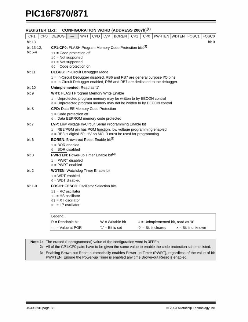
PIC16F870/871
REGISTER 11-1: CONFIGURATION WORD (ADDRESS 2007h)(1) CP1 CP0 DEBUG — WRT CPD LVP BOREN CP1 CP0 PWRTEN WDTEN FOSC1 FOSC0
bit 13 bit 0
bit 13-12,bit 5-4
CP1:CP0: FLASH Program Memory Code Protection bits(2)
11 = Code protection off10 = Not supported01 = Not supported00 = Code protection on
bit 11 DEBUG: In-Circuit Debugger Mode
1 = In-Circuit Debugger disabled, RB6 and RB7 are general purpose I/O pins0 = In-Circuit Debugger enabled, RB6 and RB7 are dedicated to the debugger
bit 10 Unimplemented: Read as ‘1’
bit 9 WRT: FLASH Program Memory Write Enable1 = Unprotected program memory may be written to by EECON control0 = Unprotected program memory may not be written to by EECON control
bit 8 CPD: Data EE Memory Code Protection
1 = Code protection off 0 = Data EEPROM memory code protected
bit 7 LVP: Low Voltage In-Circuit Serial Programming Enable bit1 = RB3/PGM pin has PGM function, low voltage programming enabled0 = RB3 is digital I/O, HV on MCLR must be used for programming
bit 6 BOREN: Brown-out Reset Enable bit(3)
1 = BOR enabled0 = BOR disabled
bit 3 PWRTEN: Power-up Timer Enable bit(3)
1 = PWRT disabled0 = PWRT enabled
bit 2 WDTEN: Watchdog Timer Enable bit1 = WDT enabled0 = WDT disabled
bit 1-0 FOSC1:FOSC0: Oscillator Selection bits11 = RC oscillator10 = HS oscillator01 = XT oscillator00 = LP oscillator
Legend:
R = Readable bit W = Writable bit U = Unimplemented bit, read as ‘0’
- n = Value at POR ‘1’ = Bit is set ‘0’ = Bit is cleared x = Bit is unknown
Note 1: The erased (unprogrammed) value of the configuration word is 3FFFh.2: All of the CP1:CP0 pairs have to be given the same value to enable the code protection scheme listed.
3: Enabling Brown-out Reset automatically enables Power-up Timer (PWRT), regardless of the value of bitPWRTEN. Ensure the Power-up Timer is enabled any time Brown-out Reset is enabled.
DS30569B-page 88 2003 Microchip Technology Inc.
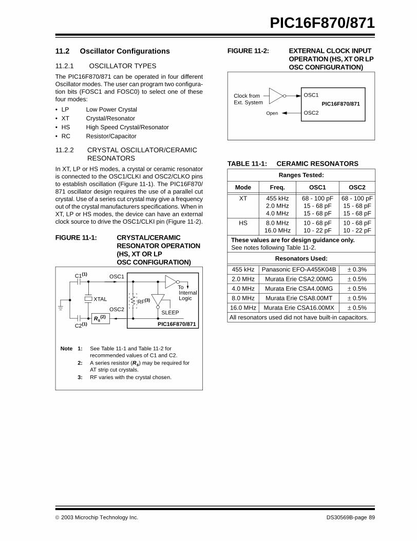
PIC16F870/871
11.2 Oscillator Configurations
11.2.1 OSCILLATOR TYPES
The PIC16F870/871 can be operated in four differentOscillator modes. The user can program two configura-tion bits (FOSC1 and FOSC0) to select one of thesefour modes:
• LP Low Power Crystal• XT Crystal/Resonator• HS High Speed Crystal/Resonator
• RC Resistor/Capacitor
11.2.2 CRYSTAL OSCILLATOR/CERAMIC RESONATORS
In XT, LP or HS modes, a crystal or ceramic resonatoris connected to the OSC1/CLKI and OSC2/CLKO pinsto establish oscillation (Figure 11-1). The PIC16F870/871 oscillator design requires the use of a parallel cutcrystal. Use of a series cut crystal may give a frequencyout of the crystal manufacturers specifications. When inXT, LP or HS modes, the device can have an externalclock source to drive the OSC1/CLKI pin (Figure 11-2).
FIGURE 11-1: CRYSTAL/CERAMIC RESONATOR OPERATION (HS, XT OR LP OSC CONFIGURATION)
FIGURE 11-2: EXTERNAL CLOCK INPUT OPERATION (HS, XT OR LP OSC CONFIGURATION)
TABLE 11-1: CERAMIC RESONATORS
Note 1: See Table 11-1 and Table 11-2 for recommended values of C1 and C2.
2: A series resistor (Rs) may be required for AT strip cut crystals.
3: RF varies with the crystal chosen.
C1(1)
C2(1)
XTAL
OSC2
OSC1
RF(3)
SLEEP
To
Logic
PIC16F870/871Rs
(2)
Internal
Ranges Tested:
Mode Freq. OSC1 OSC2
XT 455 kHz2.0 MHz4.0 MHz
68 - 100 pF15 - 68 pF15 - 68 pF
68 - 100 pF15 - 68 pF15 - 68 pF
HS 8.0 MHz16.0 MHz
10 - 68 pF10 - 22 pF
10 - 68 pF10 - 22 pF
These values are for design guidance only. See notes following Table 11-2.
Resonators Used:
455 kHz Panasonic EFO-A455K04B ± 0.3%
2.0 MHz Murata Erie CSA2.00MG ± 0.5%
4.0 MHz Murata Erie CSA4.00MG ± 0.5%
8.0 MHz Murata Erie CSA8.00MT ± 0.5%
16.0 MHz Murata Erie CSA16.00MX ± 0.5%
All resonators used did not have built-in capacitors.
OSC1
OSC2Open
Clock fromExt. System PIC16F870/871
2003 Microchip Technology Inc. DS30569B-page 89
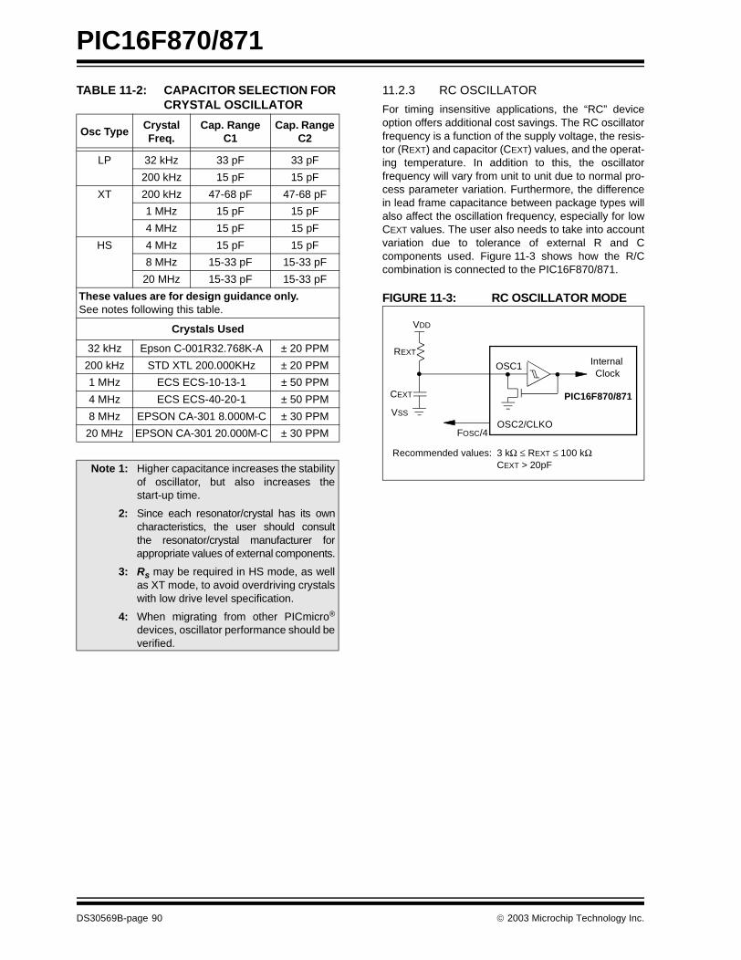
PIC16F870/871
TABLE 11-2: CAPACITOR SELECTION FOR CRYSTAL OSCILLATOR
11.2.3 RC OSCILLATOR
For timing insensitive applications, the “RC” deviceoption offers additional cost savings. The RC oscillatorfrequency is a function of the supply voltage, the resis-tor (REXT) and capacitor (CEXT) values, and the operat-ing temperature. In addition to this, the oscillatorfrequency will vary from unit to unit due to normal pro-cess parameter variation. Furthermore, the differencein lead frame capacitance between package types willalso affect the oscillation frequency, especially for lowCEXT values. The user also needs to take into accountvariation due to tolerance of external R and Ccomponents used. Figure 11-3 shows how the R/Ccombination is connected to the PIC16F870/871.
FIGURE 11-3: RC OSCILLATOR MODE
Osc TypeCrystal Freq.
Cap. Range C1
Cap. Range C2
LP 32 kHz 33 pF 33 pF
200 kHz 15 pF 15 pF
XT 200 kHz 47-68 pF 47-68 pF
1 MHz 15 pF 15 pF
4 MHz 15 pF 15 pF
HS 4 MHz 15 pF 15 pF
8 MHz 15-33 pF 15-33 pF
20 MHz 15-33 pF 15-33 pF
These values are for design guidance only. See notes following this table.
Crystals Used
32 kHz Epson C-001R32.768K-A ± 20 PPM
200 kHz STD XTL 200.000KHz ± 20 PPM
1 MHz ECS ECS-10-13-1 ± 50 PPM
4 MHz ECS ECS-40-20-1 ± 50 PPM
8 MHz EPSON CA-301 8.000M-C ± 30 PPM
20 MHz EPSON CA-301 20.000M-C ± 30 PPM
Note 1: Higher capacitance increases the stabilityof oscillator, but also increases thestart-up time.
2: Since each resonator/crystal has its owncharacteristics, the user should consultthe resonator/crystal manufacturer forappropriate values of external components.
3: Rs may be required in HS mode, as wellas XT mode, to avoid overdriving crystalswith low drive level specification.
4: When migrating from other PICmicro®
devices, oscillator performance should beverified.
OSC2/CLKO
CEXT
REXT
PIC16F870/871
OSC1
FOSC/4
InternalClock
VDD
VSS
Recommended values: 3 kΩ ≤ REXT ≤ 100 kΩCEXT > 20pF
DS30569B-page 90 2003 Microchip Technology Inc.
PIC16F870/871
11.3 RESET
The PIC16F870/871 differentiates between variouskinds of RESET:
• Power-on Reset (POR)• MCLR Reset during normal operation
• MCLR Reset during SLEEP• WDT Reset (during normal operation)• WDT Wake-up (during SLEEP)
• Brown-out Reset (BOR)
Some registers are not affected in any RESET condi-tion. Their status is unknown on POR and unchangedin any other RESET. Most other registers are reset to a“RESET state” on Power-on Reset (POR), on theMCLR and WDT Reset, on MCLR Reset during
SLEEP, and Brown-out Reset (BOR). They are notaffected by a WDT Wake-up, which is viewed as theresumption of normal operation. The TO and PD bitsare set or cleared differently in different RESET situa-tions, as indicated in Table 11-4. These bits are used insoftware to determine the nature of the RESET. SeeTable 11-6 for a full description of RESET states of allregisters.
A simplified block diagram of the On-Chip Reset Circuitis shown in Figure 11-4.
These devices have a MCLR noise filter in the MCLRReset path. The filter will detect and ignore smallpulses.
It should be noted that a WDT Reset does not driveMCLR pin low.
FIGURE 11-4: SIMPLIFIED BLOCK DIAGRAM OF ON-CHIP RESET CIRCUIT
S
R Q
ExternalRESET
MCLR
VDD
OSC1
WDTModule
VDD RiseDetect
OST/PWRT
On-chip RC OSC
WDT
Time-out
Power-on Reset
OST
10-bit Ripple Counter
PWRT
Chip_Reset
10-bit Ripple Counter
Reset
Enable OST
Enable PWRT
SLEEP
Note 1: This is a separate oscillator from the RC oscillator of the CLKI pin.
Brown-outReset BOREN
(1)
2003 Microchip Technology Inc. DS30569B-page 91
PIC16F870/871
11.4 Power-on Reset (POR)
A Power-on Reset pulse is generated on-chip whenVDD rise is detected (in the range of 1.2V - 1.7V). Totake advantage of the POR, tie the MCLR pin directly(or through a resistor) to VDD. This will eliminateexternal RC components usually needed to create aPower-on Reset. A maximum rise time for VDD isspecified. See Electrical Specifications for details.
When the device starts normal operation (exits theRESET condition), device operating parameters (volt-age, frequency, temperature,...) must be met to ensureoperation. If these conditions are not met, the devicemust be held in RESET until the operating conditionsare met. Brown-out Reset may be used to meet thestart-up conditions. For additional information, refer toApplication Note, AN007, “Power-up Trouble Shooting”(DS00007).
11.5 Power-up Timer (PWRT)
The Power-up Timer provides a fixed 72 ms nominaltime-out on power-up only from the POR. The Power-up Timer operates on an internal RC oscillator. Thechip is kept in RESET as long as the PWRT is active.The PWRT’s time delay allows VDD to rise to anacceptable level. A configuration bit is provided toenable/disable the PWRT.
The power-up time delay will vary from chip to chip dueto VDD, temperature and process variation. See DCparameters for details (TPWRT, parameter #33).
11.6 Oscillator Start-up Timer (OST)
The Oscillator Start-up Timer (OST) provides a delay of1024 oscillator cycles (from OSC1 input) after thePWRT delay is over (if PWRT is enabled). This helps toensure that the crystal oscillator or resonator hasstarted and stabilized.
The OST time-out is invoked only for XT, LP and HSmodes and only on Power-on Reset or Wake-up fromSLEEP.
11.7 Brown-out Reset (BOR)
The configuration bit, BOREN, can enable or disablethe Brown-out Reset circuit. If VDD falls below VBOR
(parameter D005, about 4V) for longer than TBOR
(parameter #35, about 100 µS), the brown-out situationwill reset the device. If VDD falls below VBOR for lessthan TBOR, a RESET may not occur.
Once the brown-out occurs, the device will remain inBrown-out Reset until VDD rises above VBOR. ThePower-up Timer then keeps the device in RESET forTPWRT (parameter #33, about 72 ms). If VDD should fallbelow VBOR during TPWRT, the Brown-out Reset pro-cess will restart when VDD rises above VBOR with thePower-up Timer Reset. The Power-up Timer is alwaysenabled when the Brown-out Reset circuit is enabled,regardless of the state of the PWRT configuration bit.
11.8 Time-out Sequence
On power-up, the time-out sequence is as follows: ThePWRT delay starts (if enabled) when a POR Resetoccurs. Then OST starts counting 1024 oscillatorcycles when PWRT ends (LP, XT, HS). When the OSTends, the device comes out of RESET.
If MCLR is kept low long enough, the time-outs willexpire. Bringing MCLR high will begin execution imme-diately. This is useful for testing purposes or to synchro-nize more than one PIC16F870/871 device operating inparallel.
Table 11-5 shows the RESET conditions for theSTATUS, PCON and PC registers, while Table 11-6shows the RESET conditions for all the registers.
11.9 Power Control/Status Register (PCON)
The Power Control/Status Register, PCON, has up totwo bits depending upon the device.
Bit0 is Brown-out Reset Status bit, BOR. Bit BOR isunknown on a Power-on Reset. It must then be set bythe user and checked on subsequent RESETS to see ifbit BOR cleared, indicating a BOR occurred. When theBrown-out Reset is disabled, the state of the BOR bit isunpredictable and is, therefore, not valid at any time.
Bit1 is POR (Power-on Reset Status bit). It is cleared ona Power-on Reset and unaffected otherwise. The usermust set this bit following a Power-on Reset.
TABLE 11-3: TIME-OUT IN VARIOUS SITUATIONS
Oscillator Configuration
Power-upBrown-out Wake-up from SLEEP
PWRTEN = 0 PWRTEN = 1
XT, HS, LP 72 ms + 1024 TOSC 1024 TOSC 72 ms + 1024 TOSC 1024 TOSC
RC 72 ms — 72 ms —
DS30569B-page 92 2003 Microchip Technology Inc.
PIC16F870/871
TABLE 11-4: STATUS BITS AND THEIR SIGNIFICANCE
TABLE 11-5: RESET CONDITION FOR SPECIAL REGISTERS
POR BOR TO PD
0 x 1 1 Power-on Reset
0 x 0 x Illegal, TO is set on POR
0 x x 0 Illegal, PD is set on POR
1 0 1 1 Brown-out Reset
1 1 0 1 WDT Reset
1 1 0 0 WDT Wake-up
1 1 u u MCLR Reset during normal operation
1 1 1 0 MCLR Reset during SLEEP or interrupt wake-up from SLEEP
Legend: x = don’t care, u = unchanged
ConditionProgramCounter
STATUSRegister
PCONRegister
Power-on Reset 000h 0001 1xxx ---- --0x
MCLR Reset during normal operation 000h 000u uuuu ---- --uu
MCLR Reset during SLEEP 000h 0001 0uuu ---- --uu
WDT Reset 000h 0000 1uuu ---- --uu
WDT Wake-up PC + 1 uuu0 0uuu ---- --uu
Brown-out Reset 000h 0001 1uuu ---- --u0
Interrupt wake-up from SLEEP PC + 1(1) uuu1 0uuu ---- --uu
Legend: u = unchanged, x = unknown, - = unimplemented bit, read as '0'Note 1: When the wake-up is due to an interrupt and the GIE bit is set, the PC is loaded with the interrupt vector (0004h).
TABLE 11-6: INITIALIZATION CONDITIONS FOR ALL REGISTERS
Register DevicesPower-on Reset,Brown-out Reset
MCLR ResetsWDT Reset
Wake-up via WDT or Interrupt
W PIC16F870 PIC16F871 xxxx xxxx uuuu uuuu uuuu uuuu
INDF PIC16F870 PIC16F871 N/A N/A N/ATMR0 PIC16F870 PIC16F871 xxxx xxxx uuuu uuuu uuuu uuuu
PCL PIC16F870 PIC16F871 0000h 0000h PC + 1(2)
STATUS PIC16F870 PIC16F871 0001 1xxx 000q quuu(3) uuuq quuu(3)
FSR PIC16F870 PIC16F871 xxxx xxxx uuuu uuuu uuuu uuuu
PORTA PIC16F870 PIC16F871 --0x 0000 --0u 0000 --uu uuuu
PORTB PIC16F870 PIC16F871 xxxx xxxx uuuu uuuu uuuu uuuu
PORTC PIC16F870 PIC16F871 xxxx xxxx uuuu uuuu uuuu uuuu
PORTD PIC16F870 PIC16F871 xxxx xxxx uuuu uuuu uuuu uuuu
PORTE PIC16F870 PIC16F871 ---- -xxx ---- -uuu ---- -uuu
PCLATH PIC16F870 PIC16F871 ---0 0000 ---0 0000 ---u uuuu
INTCON PIC16F870 PIC16F871 0000 000x 0000 000u uuuu uuuu(1)
Legend: u = unchanged, x = unknown, - = unimplemented bit, read as '0', q = value depends on condition, r = reserved, maintain clear
Note 1: One or more bits in INTCON, PIR1 and/or PIR2 will be affected (to cause wake-up).2: When the wake-up is due to an interrupt and the GIE bit is set, the PC is loaded with the interrupt vector
(0004h).3: See Table 11-5 for RESET value for specific condition.
2003 Microchip Technology Inc. DS30569B-page 93
PIC16F870/871
PIR1 PIC16F870 PIC16F871 r000 -000 r000 -000 ruuu -uuu(1)
PIC16F870 PIC16F871 0000 -000 0000 -000 uuuu -uuu(1)
PIR2 PIC16F870 PIC16F871 ---0 ---- ---0 ---- ---u ----(1)
TMR1L PIC16F870 PIC16F871 xxxx xxxx uuuu uuuu uuuu uuuu
TMR1H PIC16F870 PIC16F871 xxxx xxxx uuuu uuuu uuuu uuuu
T1CON PIC16F870 PIC16F871 --00 0000 --uu uuuu --uu uuuu
TMR2 PIC16F870 PIC16F871 0000 0000 0000 0000 uuuu uuuu
T2CON PIC16F870 PIC16F871 -000 0000 -000 0000 -uuu uuuu
CCPR1L PIC16F870 PIC16F871 xxxx xxxx uuuu uuuu uuuu uuuu
CCPR1H PIC16F870 PIC16F871 xxxx xxxx uuuu uuuu uuuu uuuu
CCP1CON PIC16F870 PIC16F871 --00 0000 --00 0000 --uu uuuu
RCSTA PIC16F870 PIC16F871 0000 000x 0000 000x uuuu uuuu
TXREG PIC16F870 PIC16F871 0000 0000 0000 0000 uuuu uuuu
RCREG PIC16F870 PIC16F871 0000 0000 0000 0000 uuuu uuuu
ADRESH PIC16F870 PIC16F871 xxxx xxxx uuuu uuuu uuuu uuuu
ADCON0 PIC16F870 PIC16F871 0000 00-0 0000 00-0 uuuu uu-u
OPTION_REG PIC16F870 PIC16F871 1111 1111 1111 1111 uuuu uuuu
TRISA PIC16F870 PIC16F871 --11 1111 --11 1111 --uu uuuu
TRISB PIC16F870 PIC16F871 1111 1111 1111 1111 uuuu uuuu
TRISC PIC16F870 PIC16F871 1111 1111 1111 1111 uuuu uuuu
TRISD PIC16F870 PIC16F871 1111 1111 1111 1111 uuuu uuuu
TRISE PIC16F870 PIC16F871 0000 -111 0000 -111 uuuu -uuu
PIE1 PIC16F870 PIC16F871 r000 -000 r000 -000 ruuu -uuu
PIC16F870 PIC16F871 0000 0000 0000 0000 uuuu uuuu
PIE2 PIC16F870 PIC16F871 ---0 ---- ---0 ---- ---u ----
PCON PIC16F870 PIC16F871 ---- --qq ---- --uu ---- --uu
PR2 PIC16F870 PIC16F871 1111 1111 1111 1111 1111 1111
TXSTA PIC16F870 PIC16F871 0000 -010 0000 -010 uuuu -uuu
SPBRG PIC16F870 PIC16F871 0000 0000 0000 0000 uuuu uuuu
ADRESL PIC16F870 PIC16F871 xxxx xxxx uuuu uuuu uuuu uuuu
ADCON1 PIC16F870 PIC16F871 0--- 0000 0--- 0000 u--- uuuu
EEDATA PIC16F870 PIC16F871 0--- 0000 0--- 0000 u--- uuuu
EEADR PIC16F870 PIC16F871 xxxx xxxx uuuu uuuu uuuu uuuu
EEDATH PIC16F870 PIC16F871 xxxx xxxx uuuu uuuu uuuu uuuu
EEADRH PIC16F870 PIC16F871 xxxx xxxx uuuu uuuu uuuu uuuu
EECON1 PIC16F870 PIC16F871 x--- x000 u--- u000 u--- uuuu
EECON2 PIC16F870 PIC16F871 ---- ---- ---- ---- ---- ----
TABLE 11-6: INITIALIZATION CONDITIONS FOR ALL REGISTERS (CONTINUED)
Register DevicesPower-on Reset,Brown-out Reset
MCLR ResetsWDT Reset
Wake-up via WDT or Interrupt
Legend: u = unchanged, x = unknown, - = unimplemented bit, read as '0', q = value depends on condition, r = reserved, maintain clear
Note 1: One or more bits in INTCON, PIR1 and/or PIR2 will be affected (to cause wake-up).2: When the wake-up is due to an interrupt and the GIE bit is set, the PC is loaded with the interrupt vector
(0004h).3: See Table 11-5 for RESET value for specific condition.
DS30569B-page 94 2003 Microchip Technology Inc.
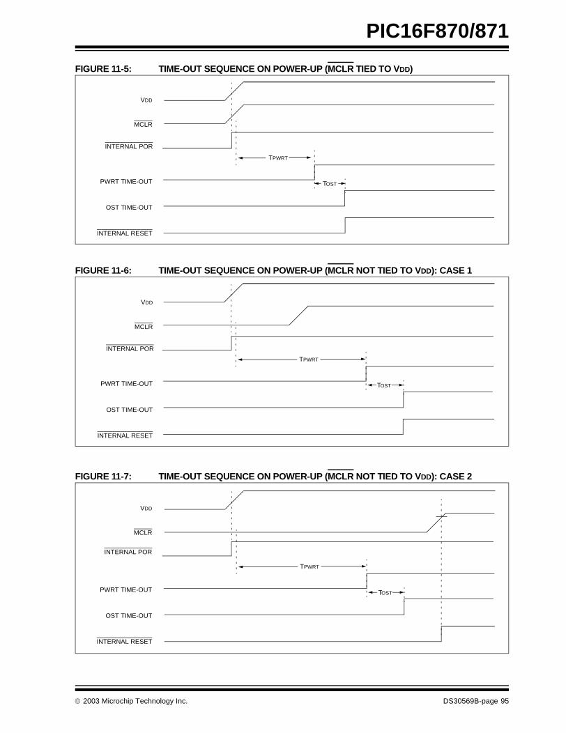
PIC16F870/871
FIGURE 11-5: TIME-OUT SEQUENCE ON POWER-UP (MCLR TIED TO VDD)
FIGURE 11-6: TIME-OUT SEQUENCE ON POWER-UP (MCLR NOT TIED TO VDD): CASE 1
FIGURE 11-7: TIME-OUT SEQUENCE ON POWER-UP (MCLR NOT TIED TO VDD): CASE 2
TPWRT
TOST
VDD
MCLR
INTERNAL POR
PWRT TIME-OUT
OST TIME-OUT
INTERNAL RESET
TPWRT
TOST
VDD
MCLR
INTERNAL POR
PWRT TIME-OUT
OST TIME-OUT
INTERNAL RESET
VDD
MCLR
INTERNAL POR
PWRT TIME-OUT
OST TIME-OUT
INTERNAL RESET
TPWRT
TOST
2003 Microchip Technology Inc. DS30569B-page 95
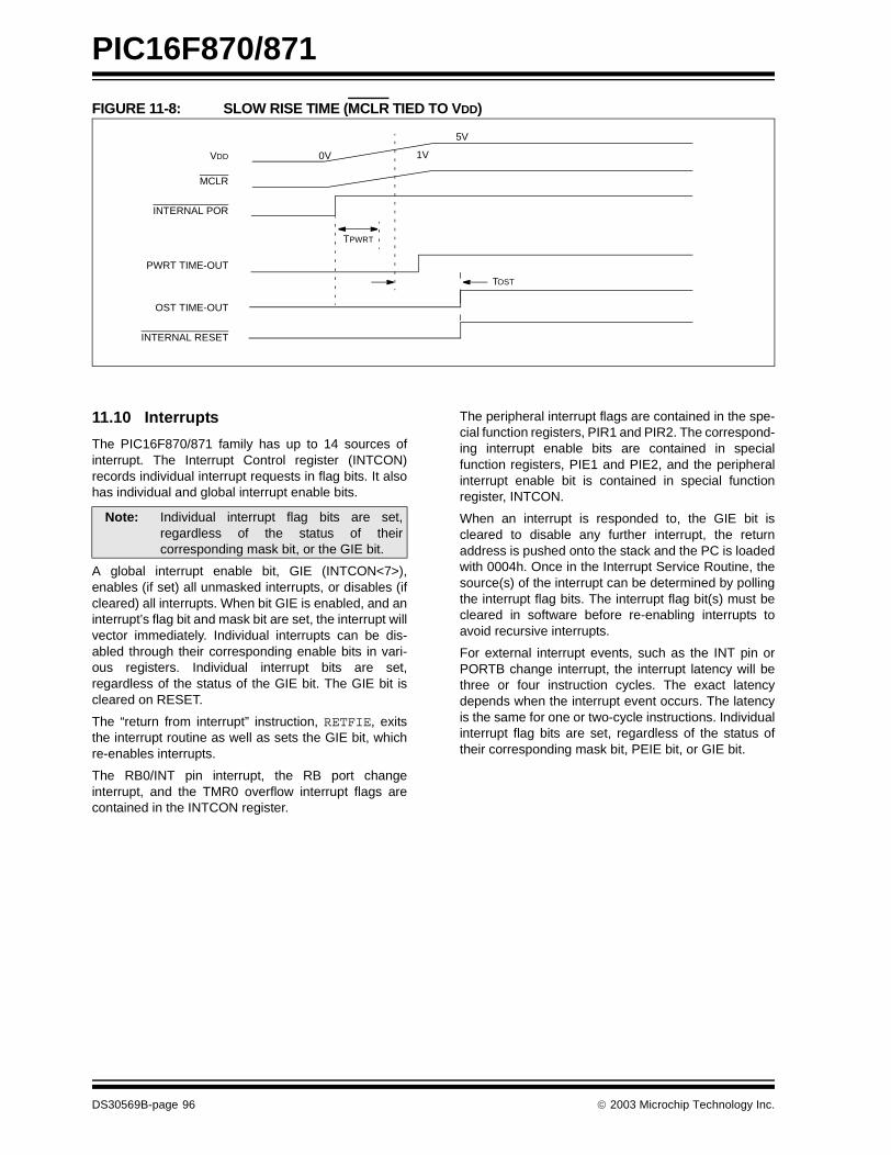
PIC16F870/871
FIGURE 11-8: SLOW RISE TIME (MCLR TIED TO VDD)
11.10 Interrupts
The PIC16F870/871 family has up to 14 sources ofinterrupt. The Interrupt Control register (INTCON)records individual interrupt requests in flag bits. It alsohas individual and global interrupt enable bits.
A global interrupt enable bit, GIE (INTCON<7>),enables (if set) all unmasked interrupts, or disables (ifcleared) all interrupts. When bit GIE is enabled, and aninterrupt’s flag bit and mask bit are set, the interrupt willvector immediately. Individual interrupts can be dis-abled through their corresponding enable bits in vari-ous registers. Individual interrupt bits are set,regardless of the status of the GIE bit. The GIE bit iscleared on RESET.
The “return from interrupt” instruction, RETFIE, exitsthe interrupt routine as well as sets the GIE bit, whichre-enables interrupts.
The RB0/INT pin interrupt, the RB port changeinterrupt, and the TMR0 overflow interrupt flags arecontained in the INTCON register.
The peripheral interrupt flags are contained in the spe-cial function registers, PIR1 and PIR2. The correspond-ing interrupt enable bits are contained in specialfunction registers, PIE1 and PIE2, and the peripheralinterrupt enable bit is contained in special functionregister, INTCON.
When an interrupt is responded to, the GIE bit iscleared to disable any further interrupt, the returnaddress is pushed onto the stack and the PC is loadedwith 0004h. Once in the Interrupt Service Routine, thesource(s) of the interrupt can be determined by pollingthe interrupt flag bits. The interrupt flag bit(s) must becleared in software before re-enabling interrupts toavoid recursive interrupts.
For external interrupt events, such as the INT pin orPORTB change interrupt, the interrupt latency will bethree or four instruction cycles. The exact latencydepends when the interrupt event occurs. The latencyis the same for one or two-cycle instructions. Individualinterrupt flag bits are set, regardless of the status oftheir corresponding mask bit, PEIE bit, or GIE bit.
VDD
MCLR
INTERNAL POR
PWRT TIME-OUT
OST TIME-OUT
INTERNAL RESET
0V 1V
5V
TPWRT
TOST
Note: Individual interrupt flag bits are set,regardless of the status of theircorresponding mask bit, or the GIE bit.
DS30569B-page 96 2003 Microchip Technology Inc.
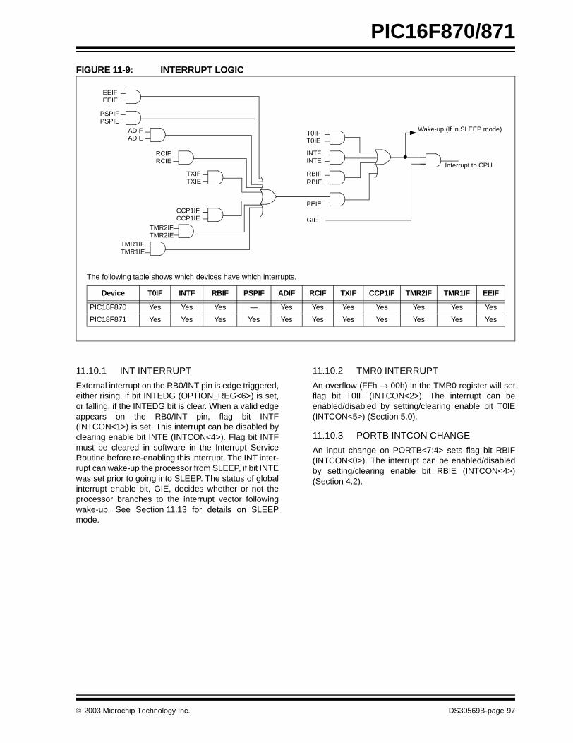
PIC16F870/871
FIGURE 11-9: INTERRUPT LOGIC
11.10.1 INT INTERRUPT
External interrupt on the RB0/INT pin is edge triggered,either rising, if bit INTEDG (OPTION_REG<6>) is set,or falling, if the INTEDG bit is clear. When a valid edgeappears on the RB0/INT pin, flag bit INTF(INTCON<1>) is set. This interrupt can be disabled byclearing enable bit INTE (INTCON<4>). Flag bit INTFmust be cleared in software in the Interrupt ServiceRoutine before re-enabling this interrupt. The INT inter-rupt can wake-up the processor from SLEEP, if bit INTEwas set prior to going into SLEEP. The status of globalinterrupt enable bit, GIE, decides whether or not theprocessor branches to the interrupt vector followingwake-up. See Section 11.13 for details on SLEEPmode.
11.10.2 TMR0 INTERRUPT
An overflow (FFh → 00h) in the TMR0 register will setflag bit T0IF (INTCON<2>). The interrupt can beenabled/disabled by setting/clearing enable bit T0IE(INTCON<5>) (Section 5.0).
11.10.3 PORTB INTCON CHANGE
An input change on PORTB<7:4> sets flag bit RBIF(INTCON<0>). The interrupt can be enabled/disabledby setting/clearing enable bit RBIE (INTCON<4>)(Section 4.2).
PSPIFPSPIE
ADIFADIE
RCIFRCIE
TXIFTXIE
CCP1IFCCP1IE
TMR2IFTMR2IE
TMR1IFTMR1IE
T0IFT0IE
INTFINTE
RBIFRBIE
GIE
PEIE
Wake-up (If in SLEEP mode)
Interrupt to CPU
The following table shows which devices have which interrupts.
Device T0IF INTF RBIF PSPIF ADIF RCIF TXIF CCP1IF TMR2IF TMR1IF EEIF
PIC18F870 Yes Yes Yes — Yes Yes Yes Yes Yes Yes Yes
PIC18F871 Yes Yes Yes Yes Yes Yes Yes Yes Yes Yes Yes
EEIFEEIE
2003 Microchip Technology Inc. DS30569B-page 97
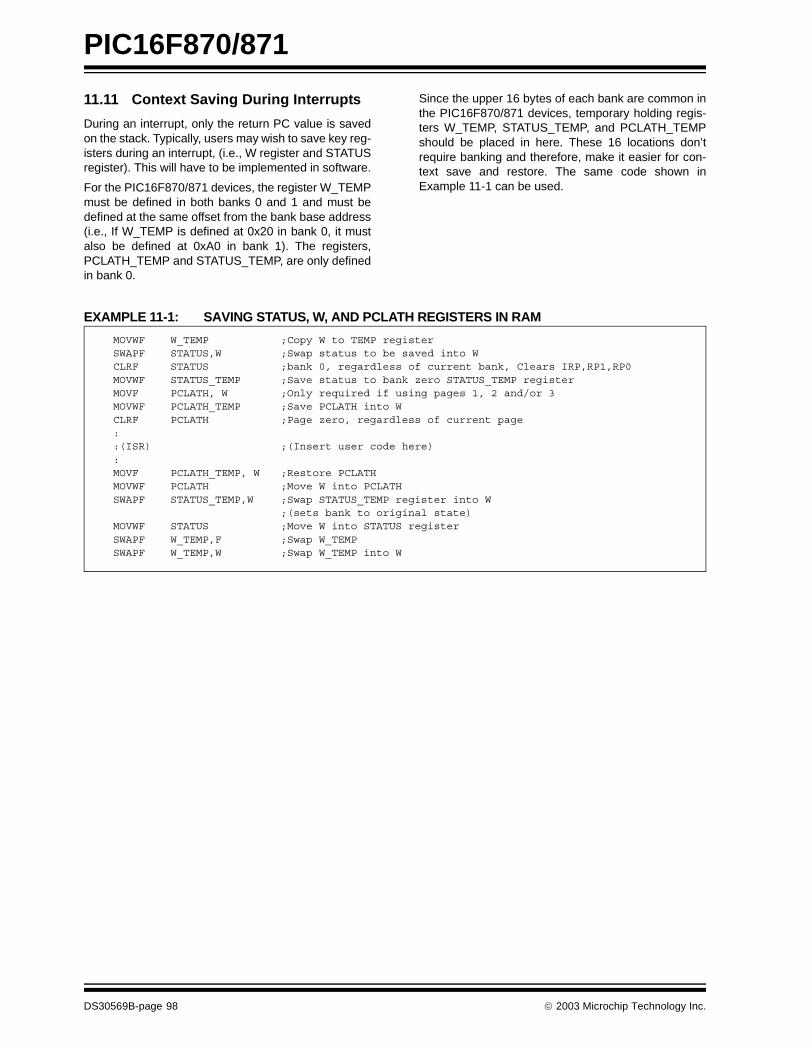
PIC16F870/871
11.11 Context Saving During Interrupts
During an interrupt, only the return PC value is savedon the stack. Typically, users may wish to save key reg-isters during an interrupt, (i.e., W register and STATUSregister). This will have to be implemented in software.
For the PIC16F870/871 devices, the register W_TEMPmust be defined in both banks 0 and 1 and must bedefined at the same offset from the bank base address(i.e., If W_TEMP is defined at 0x20 in bank 0, it mustalso be defined at 0xA0 in bank 1). The registers,PCLATH_TEMP and STATUS_TEMP, are only definedin bank 0.
Since the upper 16 bytes of each bank are common inthe PIC16F870/871 devices, temporary holding regis-ters W_TEMP, STATUS_TEMP, and PCLATH_TEMPshould be placed in here. These 16 locations don’trequire banking and therefore, make it easier for con-text save and restore. The same code shown inExample 11-1 can be used.
EXAMPLE 11-1: SAVING STATUS, W, AND PCLATH REGISTERS IN RAM
MOVWF W_TEMP ;Copy W to TEMP registerSWAPF STATUS,W ;Swap status to be saved into W CLRF STATUS ;bank 0, regardless of current bank, Clears IRP,RP1,RP0MOVWF STATUS_TEMP ;Save status to bank zero STATUS_TEMP registerMOVF PCLATH, W ;Only required if using pages 1, 2 and/or 3MOVWF PCLATH_TEMP ;Save PCLATH into WCLRF PCLATH ;Page zero, regardless of current page::(ISR) ;(Insert user code here):MOVF PCLATH_TEMP, W ;Restore PCLATHMOVWF PCLATH ;Move W into PCLATHSWAPF STATUS_TEMP,W ;Swap STATUS_TEMP register into W
;(sets bank to original state)MOVWF STATUS ;Move W into STATUS registerSWAPF W_TEMP,F ;Swap W_TEMPSWAPF W_TEMP,W ;Swap W_TEMP into W
DS30569B-page 98 2003 Microchip Technology Inc.
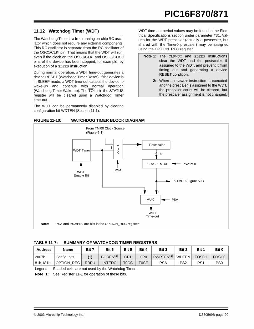
PIC16F870/871
11.12 Watchdog Timer (WDT)
The Watchdog Timer is a free running on-chip RC oscil-lator which does not require any external components.This RC oscillator is separate from the RC oscillator ofthe OSC1/CLKI pin. That means that the WDT will run,even if the clock on the OSC1/CLKI and OSC2/CLKOpins of the device has been stopped, for example, byexecution of a SLEEP instruction.
During normal operation, a WDT time-out generates adevice RESET (Watchdog Timer Reset). If the device isin SLEEP mode, a WDT time-out causes the device towake-up and continue with normal operation(Watchdog Timer Wake-up). The TO bit in the STATUSregister will be cleared upon a Watchdog Timertime-out.
The WDT can be permanently disabled by clearingconfiguration bit WDTEN (Section 11.1).
WDT time-out period values may be found in the Elec-trical Specifications section under parameter #31. Val-ues for the WDT prescaler (actually a postscaler, butshared with the Timer0 prescaler) may be assignedusing the OPTION_REG register.
FIGURE 11-10: WATCHDOG TIMER BLOCK DIAGRAM
TABLE 11-7: SUMMARY OF WATCHDOG TIMER REGISTERS
Note 1: The CLRWDT and SLEEP instructionsclear the WDT and the postscaler, ifassigned to the WDT, and prevent it fromtiming out and generating a deviceRESET condition.
2: When a CLRWDT instruction is executedand the prescaler is assigned to the WDT,the prescaler count will be cleared, butthe prescaler assignment is not changed.
From TMR0 Clock Source(Figure 5-1)
To TMR0 (Figure 5-1)
Postscaler
WDT Timer
WDT Enable Bit
0
1 MUX
PSA
8 - to - 1 MUX PS2:PS0
0 1
MUX PSA
WDTTime-out
8
Note: PSA and PS2:PS0 are bits in the OPTION_REG register.
Address Name Bit 7 Bit 6 Bit 5 Bit 4 Bit 3 Bit 2 Bit 1 Bit 0
2007h Config. bits (1) BOREN(1) CP1 CP0 PWRTEN(1) WDTEN FOSC1 FOSC0
81h,181h OPTION_REG RBPU INTEDG T0CS T0SE PSA PS2 PS1 PS0
Legend: Shaded cells are not used by the Watchdog Timer.Note 1: See Register 11-1 for operation of these bits.
2003 Microchip Technology Inc. DS30569B-page 99

PIC16F870/871
11.13 Power-down Mode (SLEEP)
Power-down mode is entered by executing a SLEEPinstruction.
If enabled, the Watchdog Timer will be cleared butkeeps running, the PD bit (STATUS<3>) is cleared, theTO (STATUS<4>) bit is set, and the oscillator driver isturned off. The I/O ports maintain the status they hadbefore the SLEEP instruction was executed (drivinghigh, low, or hi-impedance).
For lowest current consumption in this mode, place allI/O pins at either VDD or VSS, ensure no external cir-cuitry is drawing current from the I/O pin, power-downthe A/D and disable external clocks. Pull all I/O pinsthat are hi-impedance inputs, high or low externally, toavoid switching currents caused by floating inputs. TheT0CKI input should also be at VDD or VSS for lowestcurrent consumption. The contribution from on-chippull-ups on PORTB should also be considered.
The MCLR pin must be at a logic high level (VIHMC).
11.13.1 WAKE-UP FROM SLEEP
The device can wake-up from SLEEP through one ofthe following events:
1. External RESET input on MCLR pin.
2. Watchdog Timer Wake-up (if WDT wasenabled).
3. Interrupt from INT pin, RB port change orperipheral interrupt.
External MCLR Reset will cause a device RESET. Allother events are considered a continuation of programexecution and cause a “wake-up”. The TO and PD bitsin the STATUS register can be used to determine thecause of device RESET. The PD bit, which is set onpower-up, is cleared when SLEEP is invoked. The TObit is cleared if a WDT time-out occurred and causedwake-up.
The following peripheral interrupts can wake the devicefrom SLEEP:
1. PSP read or write (PIC16F874/877 only).2. TMR1 interrupt. Timer1 must be operating as an
asynchronous counter.3. CCP Capture mode interrupt.4. Special event trigger (Timer1 in Asynchronous
mode using an external clock).5. SSP (START/STOP) bit detect interrupt.
6. SSP transmit or receive in Slave mode (SPI/I2C).
7. USART RX or TX (Synchronous Slave mode).8. A/D conversion (when A/D clock source is RC).9. EEPROM write operation completion
Other peripherals cannot generate interrupts, sinceduring SLEEP, no on-chip clocks are present.
When the SLEEP instruction is being executed, the nextinstruction (PC + 1) is pre-fetched. For the device towake-up through an interrupt event, the correspondinginterrupt enable bit must be set (enabled). Wake-up isregardless of the state of the GIE bit. If the GIE bit isclear (disabled), the device continues execution at theinstruction after the SLEEP instruction. If the GIE bit isset (enabled), the device executes the instruction afterthe SLEEP instruction and then branches to the inter-rupt address (0004h). In cases where the execution ofthe instruction following SLEEP is not desirable, theuser should have a NOP after the SLEEP instruction.
11.13.2 WAKE-UP USING INTERRUPTS
When global interrupts are disabled (GIE cleared) andany interrupt source has both its interrupt enable bitand interrupt flag bit set, one of the following will occur:
• If the interrupt occurs before the execution of a SLEEP instruction, the SLEEP instruction will com-plete as a NOP. Therefore, the WDT and WDT postscaler will not be cleared, the TO bit will not be set and PD bits will not be cleared.
• If the interrupt occurs during or after the execution of a SLEEP instruction, the device will immediately wake-up from SLEEP. The SLEEP instruction will be completely executed before the wake-up. Therefore, the WDT and WDT postscaler will be cleared, the TO bit will be set and the PD bit will be cleared.
Even if the flag bits were checked before executing aSLEEP instruction, it may be possible for flag bits tobecome set before the SLEEP instruction completes. Todetermine whether a SLEEP instruction executed, testthe PD bit. If the PD bit is set, the SLEEP instructionwas executed as a NOP.
To ensure that the WDT is cleared, a CLRWDTinstruction should be executed before a SLEEPinstruction.
DS30569B-page 100 2003 Microchip Technology Inc.
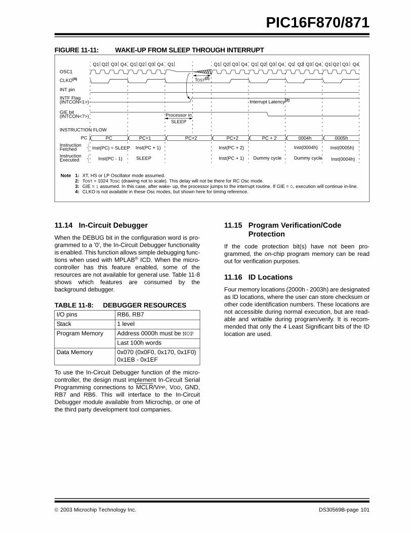
PIC16F870/871
FIGURE 11-11: WAKE-UP FROM SLEEP THROUGH INTERRUPT
11.14 In-Circuit Debugger
When the DEBUG bit in the configuration word is pro-grammed to a '0', the In-Circuit Debugger functionalityis enabled. This function allows simple debugging func-tions when used with MPLAB® ICD. When the micro-controller has this feature enabled, some of theresources are not available for general use. Table 11-8shows which features are consumed by thebackground debugger.
TABLE 11-8: DEBUGGER RESOURCES
To use the In-Circuit Debugger function of the micro-controller, the design must implement In-Circuit SerialProgramming connections to MCLR/VPP, VDD, GND,RB7 and RB6. This will interface to the In-CircuitDebugger module available from Microchip, or one ofthe third party development tool companies.
11.15 Program Verification/Code Protection
If the code protection bit(s) have not been pro-grammed, the on-chip program memory can be readout for verification purposes.
11.16 ID Locations
Four memory locations (2000h - 2003h) are designatedas ID locations, where the user can store checksum orother code identification numbers. These locations arenot accessible during normal execution, but are read-able and writable during program/verify. It is recom-mended that only the 4 Least Significant bits of the IDlocation are used.
Q1 Q2 Q3 Q4 Q1 Q2 Q3 Q4 Q1 Q1 Q2 Q3 Q4 Q1 Q2 Q3 Q4 Q1 Q2 Q3 Q4 Q1 Q2 Q3 Q4
OSC1
CLKO(4)
INT pin
INTF Flag(INTCON<1>)
GIE bit(INTCON<7>)
INSTRUCTION FLOW
PC
InstructionFetchedInstructionExecuted
PC PC+1 PC+2
Inst(PC) = SLEEP
Inst(PC - 1)
Inst(PC + 1)
SLEEP
Processor inSLEEP
Interrupt Latency(2)
Inst(PC + 2)
Inst(PC + 1)
Inst(0004h) Inst(0005h)
Inst(0004h)Dummy cycle
PC + 2 0004h 0005h
Dummy cycle
TOST(2)
PC+2
Note 1: XT, HS or LP Oscillator mode assumed.2: TOST = 1024 TOSC (drawing not to scale). This delay will not be there for RC Osc mode.3: GIE = 1 assumed. In this case, after wake- up, the processor jumps to the interrupt routine. If GIE = 0, execution will continue in-line.4: CLKO is not available in these Osc modes, but shown here for timing reference.
I/O pins RB6, RB7
Stack 1 level
Program Memory Address 0000h must be NOP
Last 100h words
Data Memory 0x070 (0x0F0, 0x170, 0x1F0)0x1EB - 0x1EF
2003 Microchip Technology Inc. DS30569B-page 101
PIC16F870/871
11.17 In-Circuit Serial Programming
PIC16F870/871 microcontrollers can be serially pro-grammed while in the end application circuit. This issimply done with two lines for clock and data and threeother lines for power, ground, and the programmingvoltage. This allows customers to manufacture boardswith unprogrammed devices, and then program themicrocontroller just before shipping the product. Thisalso allows the most recent firmware, or a customfirmware to be programmed.
When using ICSP, the part must be supplied at 4.5V to5.5V, if a bulk erase will be executed. This includesreprogramming of the code protect, both from an on-state to off-state. For all other cases of ICSP, the partmay be programmed at the normal operating voltages.This means calibration values, unique user IDs, or usercode can be reprogrammed or added.
For complete details of serial programming, pleaserefer to the EEPROM Memory ProgrammingSpecification for the PIC16F87X (DS39025).
11.18 Low Voltage ICSP Programming
The LVP bit of the configuration word enables low volt-age ICSP programming. This mode allows the micro-controller to be programmed via ICSP, using a VDD
source in the operating voltage range. This only meansthat VPP does not have to be brought to VIHH, but caninstead be left at the normal operating voltage. In thismode, the RB3/PGM pin is dedicated to the program-ming function and ceases to be a general purpose I/Opin. During programming, VDD is applied to the MCLRpin. To enter Programming mode, VDD must be appliedto the RB3/PGM pin, provided the LVP bit is set. TheLVP bit defaults to on (‘1’) from the factory.
If Low Voltage Programming mode is not used, the LVPbit can be programmed to a '0' and RB3/PGM becomesa digital I/O pin. However, the LVP bit may only be pro-grammed when programming is entered with VIHH onMCLR. The LVP bit can only be charged when usinghigh voltage on MCLR.
It should be noted, that once the LVP bit is programmedto 0, only the High Voltage Programming mode is avail-able and only High Voltage Programming mode can beused to program the device.
When using low voltage ICSP, the part must be suppliedat 4.5V to 5.5V, if a bulk erase will be executed. Thisincludes reprogramming of the code protect bits from anon-state to off-state. For all other cases of low voltageICSP, the part may be programmed at the normal oper-ating voltage. This means calibration values, uniqueuser IDs, or user code can be reprogrammed or added.
Note 1: The High Voltage Programming mode isalways available, regardless of the stateof the LVP bit, by applying VIHH to theMCLR pin.
2: While in Low Voltage ICSP mode, theRB3 pin can no longer be used as ageneral purpose I/O pin.
3: When using low voltage ICSP program-ming (LVP) and the pull-ups on PORTBare enabled, bit 3 in the TRISB registermust be cleared to disable the pull-up onRB3 and ensure the proper operation ofthe device.
4: RB3 should not be allowed to float if LVPis enabled. An external pull-down deviceshould be used to default the device tonormal Operating mode. If RB3 floatshigh, the PIC16F870/871 devices willenter Programming mode.
5: LVP mode is enabled by default on alldevices shipped from Microchip. It can bedisabled by clearing the LVP bit in theCONFIG register.
6: Disabling LVP will provide maximumcompatibility to other PIC16CXXXdevices.
DS30569B-page 102 2003 Microchip Technology Inc.
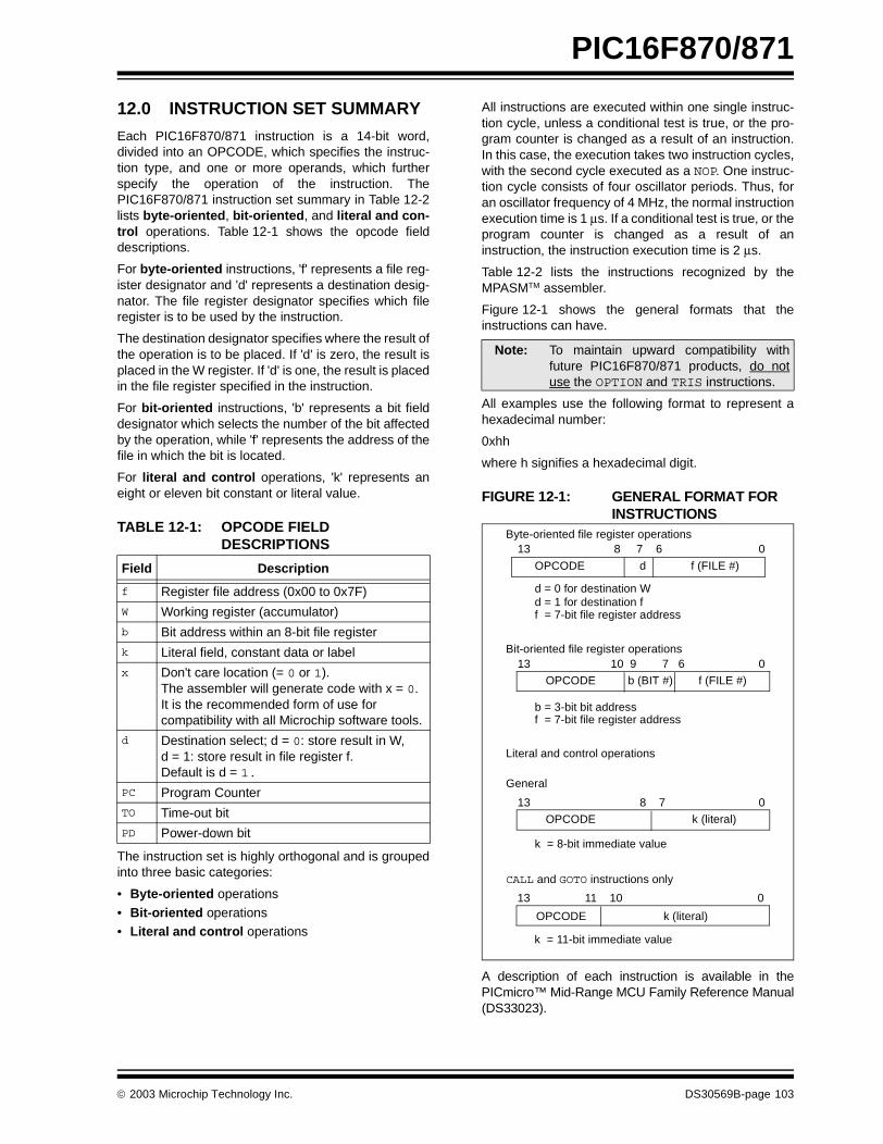
PIC16F870/871
12.0 INSTRUCTION SET SUMMARY
Each PIC16F870/871 instruction is a 14-bit word,divided into an OPCODE, which specifies the instruc-tion type, and one or more operands, which furtherspecify the operation of the instruction. ThePIC16F870/871 instruction set summary in Table 12-2lists byte-oriented, bit-oriented, and literal and con-trol operations. Table 12-1 shows the opcode fielddescriptions.
For byte-oriented instructions, 'f' represents a file reg-ister designator and 'd' represents a destination desig-nator. The file register designator specifies which fileregister is to be used by the instruction.
The destination designator specifies where the result ofthe operation is to be placed. If 'd' is zero, the result isplaced in the W register. If 'd' is one, the result is placedin the file register specified in the instruction.
For bit-oriented instructions, 'b' represents a bit fielddesignator which selects the number of the bit affectedby the operation, while 'f' represents the address of thefile in which the bit is located.
For literal and control operations, 'k' represents aneight or eleven bit constant or literal value.
TABLE 12-1: OPCODE FIELD DESCRIPTIONS
The instruction set is highly orthogonal and is groupedinto three basic categories:
• Byte-oriented operations
• Bit-oriented operations• Literal and control operations
All instructions are executed within one single instruc-tion cycle, unless a conditional test is true, or the pro-gram counter is changed as a result of an instruction.In this case, the execution takes two instruction cycles,with the second cycle executed as a NOP. One instruc-tion cycle consists of four oscillator periods. Thus, foran oscillator frequency of 4 MHz, the normal instructionexecution time is 1 µs. If a conditional test is true, or theprogram counter is changed as a result of aninstruction, the instruction execution time is 2 µs.
Table 12-2 lists the instructions recognized by theMPASMTM assembler.
Figure 12-1 shows the general formats that theinstructions can have.
All examples use the following format to represent ahexadecimal number:
0xhh
where h signifies a hexadecimal digit.
FIGURE 12-1: GENERAL FORMAT FOR INSTRUCTIONS
A description of each instruction is available in thePICmicro™ Mid-Range MCU Family Reference Manual(DS33023).
Field Description
f Register file address (0x00 to 0x7F)
W Working register (accumulator)
b Bit address within an 8-bit file register
k Literal field, constant data or label
x Don't care location (= 0 or 1). The assembler will generate code with x = 0. It is the recommended form of use for compatibility with all Microchip software tools.
d Destination select; d = 0: store result in W,d = 1: store result in file register f. Default is d = 1.
PC Program Counter
TO Time-out bit
PD Power-down bit
Note: To maintain upward compatibility withfuture PIC16F870/871 products, do notuse the OPTION and TRIS instructions.
Byte-oriented file register operations13 8 7 6 0
d = 0 for destination W
OPCODE d f (FILE #)
d = 1 for destination ff = 7-bit file register address
Bit-oriented file register operations13 10 9 7 6 0
OPCODE b (BIT #) f (FILE #)
b = 3-bit bit addressf = 7-bit file register address
Literal and control operations
13 8 7 0
OPCODE k (literal)
k = 8-bit immediate value
13 11 10 0
OPCODE k (literal)
k = 11-bit immediate value
General
CALL and GOTO instructions only
2003 Microchip Technology Inc. DS30569B-page 103
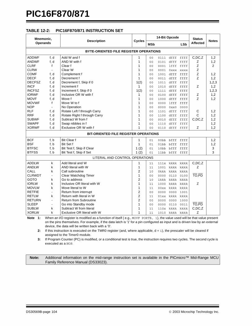
PIC16F870/871
TABLE 12-2: PIC16F870/871 INSTRUCTION SET
Mnemonic,Operands
Description Cycles14-Bit Opcode Status
AffectedNotes
MSb LSb
BYTE-ORIENTED FILE REGISTER OPERATIONS
ADDWFANDWFCLRFCLRWCOMFDECFDECFSZINCFINCFSZIORWFMOVFMOVWFNOPRLFRRFSUBWFSWAPFXORWF
f, df, d
f-
f, df, df, df, df, df, df, d
f-
f, df, df, df, df, d
Add W and fAND W with fClear fClear WComplement fDecrement fDecrement f, Skip if 0Increment fIncrement f, Skip if 0Inclusive OR W with fMove fMove W to fNo OperationRotate Left f through CarryRotate Right f through CarrySubtract W from fSwap nibbles in fExclusive OR W with f
111111
1(2)1
1(2)111111111
000000000000000000000000000000000000
011101010001000110010011101110101111010010000000000011011100001011100110
dfffdffflfff0xxxdfffdfffdfffdfffdfffdfffdffflfff0xx0dfffdfffdfffdfffdfff
ffffffffffffxxxxffffffffffffffffffffffffffffffff0000ffffffffffffffffffff
C,DC,ZZZZZZ
Z
ZZ
CC
C,DC,Z
Z
1,21,22
1,21,2
1,2,31,2
1,2,31,21,2
1,21,21,21,21,2
BIT-ORIENTED FILE REGISTER OPERATIONS
BCFBSFBTFSCBTFSS
f, bf, bf, bf, b
Bit Clear fBit Set fBit Test f, Skip if ClearBit Test f, Skip if Set
11
1 (2)1 (2)
01010101
00bb01bb10bb11bb
bfffbfffbfffbfff
ffffffffffffffff
1,21,233
LITERAL AND CONTROL OPERATIONS
ADDLWANDLWCALLCLRWDTGOTOIORLWMOVLWRETFIERETLWRETURNSLEEPSUBLWXORLW
kkk-kkk-k--kk
Add literal and WAND literal with WCall subroutineClear Watchdog TimerGo to addressInclusive OR literal with WMove literal to WReturn from interruptReturn with literal in W Return from SubroutineGo into Standby modeSubtract W from literalExclusive OR literal with W
1121211222111
11111000101111001100001111
111x10010kkk00001kkk100000xx000001xx00000000110x1010
kkkkkkkkkkkk0110kkkkkkkkkkkk0000kkkk00000110kkkkkkkk
kkkkkkkkkkkk0100kkkkkkkkkkkk1001kkkk10000011kkkkkkkk
C,DC,ZZ
TO,PD
Z
TO,PDC,DC,Z
Z
Note 1: When an I/O register is modified as a function of itself ( e.g., MOVF PORTB, 1), the value used will be that value present on the pins themselves. For example, if the data latch is '1' for a pin configured as input and is driven low by an external device, the data will be written back with a '0'.
2: If this instruction is executed on the TMR0 register (and, where applicable, d = 1), the prescaler will be cleared if assigned to the Timer0 module.
3: If Program Counter (PC) is modified, or a conditional test is true, the instruction requires two cycles. The second cycle is executed as a NOP.
Note: Additional information on the mid-range instruction set is available in the PICmicro™ Mid-Range MCUFamily Reference Manual (DS33023).
DS30569B-page 104 2003 Microchip Technology Inc.
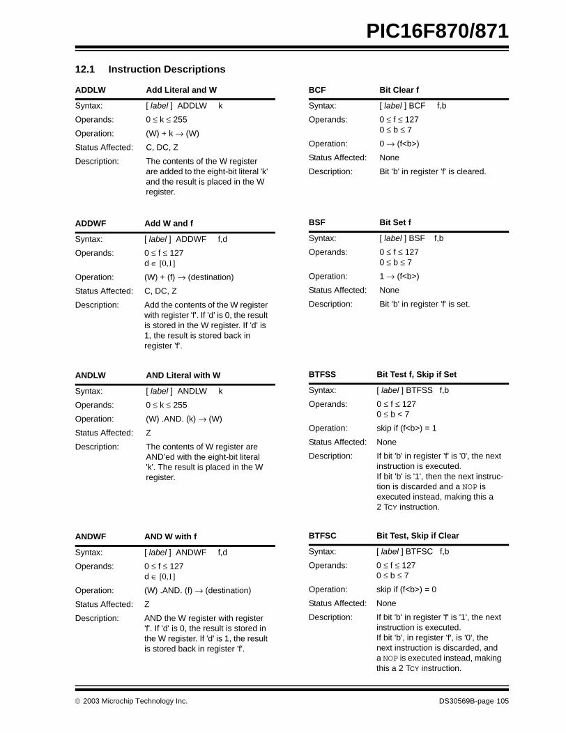
PIC16F870/871
12.1 Instruction Descriptions
ADDLW Add Literal and W
Syntax: [ label ] ADDLW k
Operands: 0 ≤ k ≤ 255
Operation: (W) + k → (W)
Status Affected: C, DC, Z
Description: The contents of the W register are added to the eight-bit literal 'k' and the result is placed in the W register.
ADDWF Add W and f
Syntax: [ label ] ADDWF f,d
Operands: 0 ≤ f ≤ 127d ∈ [0,1]
Operation: (W) + (f) → (destination)
Status Affected: C, DC, Z
Description: Add the contents of the W register with register 'f'. If 'd' is 0, the result is stored in the W register. If 'd' is 1, the result is stored back in register 'f'.
ANDLW AND Literal with W
Syntax: [ label ] ANDLW k
Operands: 0 ≤ k ≤ 255
Operation: (W) .AND. (k) → (W)
Status Affected: Z
Description: The contents of W register are AND’ed with the eight-bit literal 'k'. The result is placed in the W register.
ANDWF AND W with f
Syntax: [ label ] ANDWF f,d
Operands: 0 ≤ f ≤ 127d ∈ [0,1]
Operation: (W) .AND. (f) → (destination)
Status Affected: Z
Description: AND the W register with register 'f'. If 'd' is 0, the result is stored in the W register. If 'd' is 1, the result is stored back in register 'f'.
BCF Bit Clear f
Syntax: [ label ] BCF f,b
Operands: 0 ≤ f ≤ 1270 ≤ b ≤ 7
Operation: 0 → (f<b>)
Status Affected: None
Description: Bit 'b' in register 'f' is cleared.
BSF Bit Set f
Syntax: [ label ] BSF f,b
Operands: 0 ≤ f ≤ 1270 ≤ b ≤ 7
Operation: 1 → (f<b>)
Status Affected: None
Description: Bit 'b' in register 'f' is set.
BTFSS Bit Test f, Skip if Set
Syntax: [ label ] BTFSS f,b
Operands: 0 ≤ f ≤ 1270 ≤ b < 7
Operation: skip if (f<b>) = 1
Status Affected: None
Description: If bit 'b' in register 'f' is '0', the next instruction is executed.If bit 'b' is '1', then the next instruc-tion is discarded and a NOP is executed instead, making this a 2 TCY instruction.
BTFSC Bit Test, Skip if Clear
Syntax: [ label ] BTFSC f,b
Operands: 0 ≤ f ≤ 1270 ≤ b ≤ 7
Operation: skip if (f<b>) = 0
Status Affected: None
Description: If bit 'b' in register 'f' is '1', the next instruction is executed.If bit 'b', in register 'f', is '0', the next instruction is discarded, and a NOP is executed instead, making this a 2 TCY instruction.
2003 Microchip Technology Inc. DS30569B-page 105
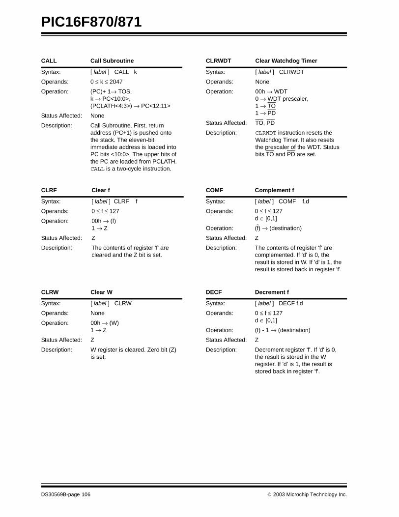
PIC16F870/871
CALL Call Subroutine
Syntax: [ label ] CALL k
Operands: 0 ≤ k ≤ 2047
Operation: (PC)+ 1→ TOS,k → PC<10:0>,(PCLATH<4:3>) → PC<12:11>
Status Affected: None
Description: Call Subroutine. First, return address (PC+1) is pushed onto the stack. The eleven-bit immediate address is loaded into PC bits <10:0>. The upper bits of the PC are loaded from PCLATH. CALL is a two-cycle instruction.
CLRF Clear f
Syntax: [ label ] CLRF f
Operands: 0 ≤ f ≤ 127
Operation: 00h → (f)1 → Z
Status Affected: Z
Description: The contents of register 'f' are cleared and the Z bit is set.
CLRW Clear W
Syntax: [ label ] CLRW
Operands: None
Operation: 00h → (W)1 → Z
Status Affected: Z
Description: W register is cleared. Zero bit (Z) is set.
CLRWDT Clear Watchdog Timer
Syntax: [ label ] CLRWDT
Operands: None
Operation: 00h → WDT0 → WDT prescaler,1 → TO1 → PD
Status Affected: TO, PD
Description: CLRWDT instruction resets the Watchdog Timer. It also resets the prescaler of the WDT. Status bits TO and PD are set.
COMF Complement f
Syntax: [ label ] COMF f,d
Operands: 0 ≤ f ≤ 127d ∈ [0,1]
Operation: (f) → (destination)
Status Affected: Z
Description: The contents of register 'f' are complemented. If 'd' is 0, the result is stored in W. If 'd' is 1, the result is stored back in register 'f'.
DECF Decrement f
Syntax: [ label ] DECF f,d
Operands: 0 ≤ f ≤ 127d ∈ [0,1]
Operation: (f) - 1 → (destination)
Status Affected: Z
Description: Decrement register 'f'. If 'd' is 0, the result is stored in the W register. If 'd' is 1, the result is stored back in register 'f'.
DS30569B-page 106 2003 Microchip Technology Inc.
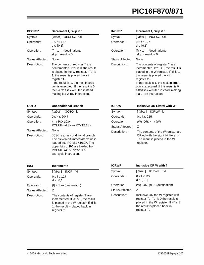
PIC16F870/871
DECFSZ Decrement f, Skip if 0
Syntax: [ label ] DECFSZ f,d
Operands: 0 ≤ f ≤ 127d ∈ [0,1]
Operation: (f) - 1 → (destination); skip if result = 0
Status Affected: None
Description: The contents of register 'f' are decremented. If 'd' is 0, the result is placed in the W register. If 'd' is 1, the result is placed back in register 'f'. If the result is 1, the next instruc-tion is executed. If the result is 0, then a NOP is executed instead making it a 2 TCY instruction.
GOTO Unconditional Branch
Syntax: [ label ] GOTO k
Operands: 0 ≤ k ≤ 2047
Operation: k → PC<10:0>PCLATH<4:3> → PC<12:11>
Status Affected: None
Description: GOTO is an unconditional branch. The eleven-bit immediate value is loaded into PC bits <10:0>. The upper bits of PC are loaded from PCLATH<4:3>. GOTO is a two-cycle instruction.
INCF Increment f
Syntax: [ label ] INCF f,d
Operands: 0 ≤ f ≤ 127d ∈ [0,1]
Operation: (f) + 1 → (destination)
Status Affected: Z
Description: The contents of register 'f' are incremented. If 'd' is 0, the result is placed in the W register. If 'd' is 1, the result is placed back in register 'f'.
INCFSZ Increment f, Skip if 0
Syntax: [ label ] INCFSZ f,d
Operands: 0 ≤ f ≤ 127d ∈ [0,1]
Operation: (f) + 1 → (destination), skip if result = 0
Status Affected: None
Description: The contents of register 'f' are incremented. If 'd' is 0, the result is placed in the W register. If 'd' is 1, the result is placed back in register 'f'.If the result is 1, the next instruc-tion is executed. If the result is 0, a NOP is executed instead, making it a 2 TCY instruction.
IORLW Inclusive OR Literal with W
Syntax: [ label ] IORLW k
Operands: 0 ≤ k ≤ 255
Operation: (W) .OR. k → (W)
Status Affected: Z
Description: The contents of the W register are OR’ed with the eight bit literal 'k'. The result is placed in the W register.
IORWF Inclusive OR W with f
Syntax: [ label ] IORWF f,d
Operands: 0 ≤ f ≤ 127d ∈ [0,1]
Operation: (W) .OR. (f) → (destination)
Status Affected: Z
Description: Inclusive OR the W register with register 'f'. If 'd' is 0 the result is placed in the W register. If 'd' is 1 the result is placed back in register 'f'.
2003 Microchip Technology Inc. DS30569B-page 107
PIC16F870/871
MOVF Move f
Syntax: [ label ] MOVF f,d
Operands: 0 ≤ f ≤ 127d ∈ [0,1]
Operation: (f) → (destination)
Status Affected: Z
Description: The contents of register f are moved to a destination dependant upon the status of d. If d = 0, destination is W register. If d = 1, the destination is file register f itself. d = 1 is useful to test a file register, since status flag Z is affected.
MOVLW Move Literal to W
Syntax: [ label ] MOVLW k
Operands: 0 ≤ k ≤ 255
Operation: k → (W)
Status Affected: None
Description: The eight-bit literal 'k' is loaded into W register. The don’t cares will assemble as 0’s.
MOVWF Move W to f
Syntax: [ label ] MOVWF f
Operands: 0 ≤ f ≤ 127
Operation: (W) → (f)
Status Affected: None
Description: Move data from W register to register 'f'.
NOP No Operation
Syntax: [ label ] NOP
Operands: None
Operation: No operation
Status Affected: None
Description: No operation.
RETFIE Return from Interrupt
Syntax: [ label ] RETFIE
Operands: None
Operation: TOS → PC,1 → GIE
Status Affected: None
RETLW Return with Literal in W
Syntax: [ label ] RETLW k
Operands: 0 ≤ k ≤ 255
Operation: k → (W); TOS → PC
Status Affected: None
Description: The W register is loaded with the eight-bit literal 'k'. The program counter is loaded from the top of the stack (the return address). This is a two-cycle instruction.
DS30569B-page 108 2003 Microchip Technology Inc.
PIC16F870/871
RLF Rotate Left f through Carry
Syntax: [ label ] RLF f,d
Operands: 0 ≤ f ≤ 127d ∈ [0,1]
Operation: See description below
Status Affected: C
Description: The contents of register 'f' are rotated one bit to the left through the Carry Flag. If 'd' is 0, the result is placed in the W register. If 'd' is 1, the result is stored back in register 'f'.
RETURN Return from Subroutine
Syntax: [ label ] RETURN
Operands: None
Operation: TOS → PC
Status Affected: None
Description: Return from subroutine. The stack is POPed and the top of the stack (TOS) is loaded into the program counter. This is a two-cycle instruction.
RRF Rotate Right f through Carry
Syntax: [ label ] RRF f,d
Operands: 0 ≤ f ≤ 127d ∈ [0,1]
Operation: See description below
Status Affected: C
Description: The contents of register 'f' are rotated one bit to the right through the Carry Flag. If 'd' is 0, the result is placed in the W register. If 'd' is 1, the result is placed back in register 'f'.
Register fC
Register fC
SLEEP
Syntax: [ label ] SLEEP
Operands: None
Operation: 00h → WDT,0 → WDT prescaler,1 → TO,0 → PD
Status Affected: TO, PD
Description: The power-down status bit, PD is cleared. Time-out status bit, TO is set. Watchdog Timer and its prescaler are cleared.The processor is put into SLEEP mode with the oscillator stopped.
SUBLW Subtract W from Literal
Syntax: [ label ] SUBLW k
Operands: 0 ≤ k ≤ 255
Operation: k - (W) → (W)
Status Affected: C, DC, Z
Description: The W register is subtracted (2’s complement method) from the eight-bit literal 'k'. The result is placed in the W register.
SUBWF Subtract W from f
Syntax: [ label ] SUBWF f,d
Operands: 0 ≤ f ≤ 127d ∈ [0,1]
Operation: (f) - (W) → (destination)
Status Affected:
C, DC, Z
Description: Subtract (2’s complement method) W register from register 'f'. If 'd' is 0, the result is stored in the W register. If 'd' is 1, the result is stored back in register 'f'.
2003 Microchip Technology Inc. DS30569B-page 109

PIC16F870/871
SWAPF Swap Nibbles in f
Syntax: [ label ] SWAPF f,d
Operands: 0 ≤ f ≤ 127d ∈ [0,1]
Operation: (f<3:0>) → (destination<7:4>),(f<7:4>) → (destination<3:0>)
Status Affected: None
Description: The upper and lower nibbles of register 'f' are exchanged. If 'd' is 0, the result is placed in the W register. If 'd' is 1, the result is placed in register 'f'.
XORLW Exclusive OR Literal with W
Syntax: [ label ] XORLW k
Operands: 0 ≤ k ≤ 255
Operation: (W) .XOR. k → (W)
Status Affected: Z
Description: The contents of the W register are XOR’ed with the eight-bit literal 'k'. The result is placed in the W register.
XORWF Exclusive OR W with f
Syntax: [ label ] XORWF f,d
Operands: 0 ≤ f ≤ 127d ∈ [0,1]
Operation: (W) .XOR. (f) → (destination)
Status Affected: Z
Description: Exclusive OR the contents of the W register with register 'f'. If 'd' is 0, the result is stored in the W register. If 'd' is 1, the result is stored back in register 'f'.
DS30569B-page 110 2003 Microchip Technology Inc.
PIC16F870/871
13.0 DEVELOPMENT SUPPORT
The PICmicro® microcontrollers are supported with afull range of hardware and software development tools:
• Integrated Development Environment
- MPLAB® IDE Software• Assemblers/Compilers/Linkers
- MPASMTM Assembler
- MPLAB C17 and MPLAB C18 C Compilers- MPLINKTM Object Linker/
MPLIBTM Object Librarian- MPLAB C30 C Compiler- MPLAB ASM30 Assembler/Linker/Library
• Simulators- MPLAB SIM Software Simulator- MPLAB dsPIC30 Software Simulator
• Emulators- MPLAB ICE 2000 In-Circuit Emulator- MPLAB ICE 4000 In-Circuit Emulator
• In-Circuit Debugger- MPLAB ICD 2
• Device Programmers
- PRO MATE® II Universal Device Programmer- PICSTART® Plus Development Programmer
• Low Cost Demonstration Boards
- PICDEMTM 1 Demonstration Board- PICDEM.netTM Demonstration Board- PICDEM 2 Plus Demonstration Board
- PICDEM 3 Demonstration Board- PICDEM 4 Demonstration Board- PICDEM 17 Demonstration Board
- PICDEM 18R Demonstration Board- PICDEM LIN Demonstration Board- PICDEM USB Demonstration Board
• Evaluation Kits- KEELOQ®
- PICDEM MSC
- microID®
- CAN- PowerSmart®
- Analog
13.1 MPLAB Integrated Development Environment Software
The MPLAB IDE software brings an ease of softwaredevelopment previously unseen in the 8/16-bit micro-controller market. The MPLAB IDE is a Windows®
based application that contains:
• An interface to debugging tools- simulator- programmer (sold separately)
- emulator (sold separately)- in-circuit debugger (sold separately)
• A full-featured editor with color coded context
• A multiple project manager• Customizable data windows with direct edit of
contents• High level source code debugging• Mouse over variable inspection
• Extensive on-line help
The MPLAB IDE allows you to:
• Edit your source files (either assembly or C)• One touch assemble (or compile) and download
to PICmicro emulator and simulator tools (automatically updates all project information)
• Debug using:- source files (assembly or C)- absolute listing file (mixed assembly and C)
- machine code
MPLAB IDE supports multiple debugging tools in asingle development paradigm, from the cost effectivesimulators, through low cost in-circuit debuggers, tofull-featured emulators. This eliminates the learningcurve when upgrading to tools with increasing flexibilityand power.
13.2 MPASM Assembler
The MPASM assembler is a full-featured, universalmacro assembler for all PICmicro MCUs.
The MPASM assembler generates relocatable objectfiles for the MPLINK object linker, Intel® standard HEXfiles, MAP files to detail memory usage and symbol ref-erence, absolute LST files that contain source lines andgenerated machine code and COFF files fordebugging.
The MPASM assembler features include:
• Integration into MPLAB IDE projects• User defined macros to streamline assembly code
• Conditional assembly for multi-purpose source files
• Directives that allow complete control over the assembly process
2003 Microchip Technology Inc. DS30569B-page 111
PIC16F870/871
13.3 MPLAB C17 and MPLAB C18 C Compilers
The MPLAB C17 and MPLAB C18 Code DevelopmentSystems are complete ANSI C compilers forMicrochip’s PIC17CXXX and PIC18CXXX family ofmicrocontrollers. These compilers provide powerfulintegration capabilities, superior code optimization andease of use not found with other compilers.
For easy source level debugging, the compilers providesymbol information that is optimized to the MPLAB IDEdebugger.
13.4 MPLINK Object Linker/MPLIB Object Librarian
The MPLINK object linker combines relocatableobjects created by the MPASM assembler and theMPLAB C17 and MPLAB C18 C compilers. It can linkrelocatable objects from pre-compiled libraries, usingdirectives from a linker script.
The MPLIB object librarian manages the creation andmodification of library files of pre-compiled code. Whena routine from a library is called from a source file, onlythe modules that contain that routine will be linked inwith the application. This allows large libraries to beused efficiently in many different applications.
The object linker/library features include:
• Efficient linking of single libraries instead of many smaller files
• Enhanced code maintainability by grouping related modules together
• Flexible creation of libraries with easy module listing, replacement, deletion and extraction
13.5 MPLAB C30 C Compiler
The MPLAB C30 C compiler is a full-featured, ANSIcompliant, optimizing compiler that translates standardANSI C programs into dsPIC30F assembly languagesource. The compiler also supports many command-line options and language extensions to take fulladvantage of the dsPIC30F device hardware capabili-ties, and afford fine control of the compiler codegenerator.
MPLAB C30 is distributed with a complete ANSI Cstandard library. All library functions have been vali-dated and conform to the ANSI C library standard. Thelibrary includes functions for string manipulation,dynamic memory allocation, data conversion, time-keeping, and math functions (trigonometric, exponen-tial and hyperbolic). The compiler provides symbolicinformation for high level source debugging with theMPLAB IDE.
13.6 MPLAB ASM30 Assembler, Linker, and Librarian
MPLAB ASM30 assembler produces relocatablemachine code from symbolic assembly language fordsPIC30F devices. MPLAB C30 compiler uses theassembler to produce it’s object file. The assemblergenerates relocatable object files that can then bearchived or linked with other relocatable object files andarchives to create an executable file. Notable featuresof the assembler include:
• Support for the entire dsPIC30F instruction set
• Support for fixed-point and floating-point data• Command line interface• Rich directive set
• Flexible macro language• MPLAB IDE compatibility
13.7 MPLAB SIM Software Simulator
The MPLAB SIM software simulator allows code devel-opment in a PC hosted environment by simulating thePICmicro series microcontrollers on an instructionlevel. On any given instruction, the data areas can beexamined or modified and stimuli can be applied froma file, or user defined key press, to any pin. The execu-tion can be performed in Single-Step, Execute UntilBreak, or Trace mode.
The MPLAB SIM simulator fully supports symbolicdebugging using the MPLAB C17 and MPLAB C18C Compilers, as well as the MPASM assembler. Thesoftware simulator offers the flexibility to develop anddebug code outside of the laboratory environment,making it an excellent, economical softwaredevelopment tool.
13.8 MPLAB SIM30 Software Simulator
The MPLAB SIM30 software simulator allows codedevelopment in a PC hosted environment by simulatingthe dsPIC30F series microcontrollers on an instructionlevel. On any given instruction, the data areas can beexamined or modified and stimuli can be applied froma file, or user defined key press, to any of the pins.
The MPLAB SIM30 simulator fully supports symbolicdebugging using the MPLAB C30 C Compiler andMPLAB ASM30 assembler. The simulator runs in eithera Command Line mode for automated tasks, or fromMPLAB IDE. This high speed simulator is designed todebug, analyze and optimize time intensive DSProutines.
DS30569B-page 112 2003 Microchip Technology Inc.
PIC16F870/871
13.9 MPLAB ICE 2000 High Performance Universal In-Circuit Emulator
The MPLAB ICE 2000 universal in-circuit emulator isintended to provide the product development engineerwith a complete microcontroller design tool set forPICmicro microcontrollers. Software control of theMPLAB ICE 2000 in-circuit emulator is advanced bythe MPLAB Integrated Development Environment,which allows editing, building, downloading and sourcedebugging from a single environment.
The MPLAB ICE 2000 is a full-featured emulator sys-tem with enhanced trace, trigger and data monitoringfeatures. Interchangeable processor modules allow thesystem to be easily reconfigured for emulation of differ-ent processors. The universal architecture of theMPLAB ICE in-circuit emulator allows expansion tosupport new PICmicro microcontrollers.
The MPLAB ICE 2000 in-circuit emulator system hasbeen designed as a real-time emulation system withadvanced features that are typically found on moreexpensive development tools. The PC platform andMicrosoft® Windows 32-bit operating system werechosen to best make these features available in asimple, unified application.
13.10 MPLAB ICE 4000 High Performance Universal In-Circuit Emulator
The MPLAB ICE 4000 universal in-circuit emulator isintended to provide the product development engineerwith a complete microcontroller design tool set for high-end PICmicro microcontrollers. Software control of theMPLAB ICE in-circuit emulator is provided by theMPLAB Integrated Development Environment, whichallows editing, building, downloading and sourcedebugging from a single environment.
The MPLAB ICD 4000 is a premium emulator system,providing the features of MPLAB ICE 2000, but withincreased emulation memory and high speed perfor-mance for dsPIC30F and PIC18XXXX devices. Itsadvanced emulator features include complex triggeringand timing, up to 2 Mb of emulation memory, and theability to view variables in real-time.
The MPLAB ICE 4000 in-circuit emulator system hasbeen designed as a real-time emulation system withadvanced features that are typically found on moreexpensive development tools. The PC platform andMicrosoft Windows 32-bit operating system were cho-sen to best make these features available in a simple,unified application.
13.11 MPLAB ICD 2 In-Circuit Debugger
Microchip’s In-Circuit Debugger, MPLAB ICD 2, is apowerful, low cost, run-time development tool,connecting to the host PC via an RS-232 or high speedUSB interface. This tool is based on the FLASHPICmicro MCUs and can be used to develop for theseand other PICmicro microcontrollers. The MPLABICD 2 utilizes the in-circuit debugging capability builtinto the FLASH devices. This feature, along withMicrochip’s In-Circuit Serial ProgrammingTM (ICSPTM)protocol, offers cost effective in-circuit FLASH debug-ging from the graphical user interface of the MPLABIntegrated Development Environment. This enables adesigner to develop and debug source code by settingbreakpoints, single-stepping and watching variables,CPU status and peripheral registers. Running at fullspeed enables testing hardware and applications inreal-time. MPLAB ICD 2 also serves as a developmentprogrammer for selected PICmicro devices.
13.12 PRO MATE II Universal Device Programmer
The PRO MATE II is a universal, CE compliant deviceprogrammer with programmable voltage verification atVDDMIN and VDDMAX for maximum reliability. It featuresan LCD display for instructions and error messagesand a modular detachable socket assembly to supportvarious package types. In Stand-Alone mode, thePRO MATE II device programmer can read, verify, andprogram PICmicro devices without a PC connection. Itcan also set code protection in this mode.
13.13 PICSTART Plus Development Programmer
The PICSTART Plus development programmer is aneasy-to-use, low cost, prototype programmer. It con-nects to the PC via a COM (RS-232) port. MPLABIntegrated Development Environment software makesusing the programmer simple and efficient. ThePICSTART Plus development programmer supportsmost PICmicro devices up to 40 pins. Larger pin countdevices, such as the PIC16C92X and PIC17C76X,may be supported with an adapter socket. ThePICSTART Plus development programmer is CEcompliant.
2003 Microchip Technology Inc. DS30569B-page 113
PIC16F870/871
13.14 PICDEM 1 PICmicroDemonstration Board
The PICDEM 1 demonstration board demonstrates thecapabilities of the PIC16C5X (PIC16C54 toPIC16C58A), PIC16C61, PIC16C62X, PIC16C71,PIC16C8X, PIC17C42, PIC17C43 and PIC17C44. Allnecessary hardware and software is included to runbasic demo programs. The sample microcontrollersprovided with the PICDEM 1 demonstration board canbe programmed with a PRO MATE II device program-mer, or a PICSTART Plus development programmer.The PICDEM 1 demonstration board can be connectedto the MPLAB ICE in-circuit emulator for testing. A pro-totype area extends the circuitry for additional applica-tion components. Features include an RS-232interface, a potentiometer for simulated analog input,push button switches and eight LEDs.
13.15 PICDEM.net Internet/Ethernet Demonstration Board
The PICDEM.net demonstration board is an Internet/Ethernet demonstration board using the PIC18F452microcontroller and TCP/IP firmware. The boardsupports any 40-pin DIP device that conforms to thestandard pinout used by the PIC16F877 orPIC18C452. This kit features a user friendly TCP/IPstack, web server with HTML, a 24L256 SerialEEPROM for Xmodem download to web pages intoSerial EEPROM, ICSP/MPLAB ICD 2 interface con-nector, an Ethernet interface, RS-232 interface, and a16 x 2 LCD display. Also included is the book andCD-ROM “TCP/IP Lean, Web Servers for EmbeddedSystems,” by Jeremy Bentham
13.16 PICDEM 2 Plus Demonstration Board
The PICDEM 2 Plus demonstration board supportsmany 18-, 28-, and 40-pin microcontrollers, includingPIC16F87X and PIC18FXX2 devices. All the neces-sary hardware and software is included to run the dem-onstration programs. The sample microcontrollersprovided with the PICDEM 2 demonstration board canbe programmed with a PRO MATE II device program-mer, PICSTART Plus development programmer, orMPLAB ICD 2 with a Universal Programmer Adapter.The MPLAB ICD 2 and MPLAB ICE in-circuit emulatorsmay also be used with the PICDEM 2 demonstrationboard to test firmware. A prototype area extends thecircuitry for additional application components. Someof the features include an RS-232 interface, a 2 x 16LCD display, a piezo speaker, an on-board temperaturesensor, four LEDs, and sample PIC18F452 andPIC16F877 FLASH microcontrollers.
13.17 PICDEM 3 PIC16C92X Demonstration Board
The PICDEM 3 demonstration board supports thePIC16C923 and PIC16C924 in the PLCC package. Allthe necessary hardware and software is included to runthe demonstration programs.
13.18 PICDEM 4 8/14/18-Pin Demonstration Board
The PICDEM 4 can be used to demonstrate the capa-bilities of the 8-, 14-, and 18-pin PIC16XXXX andPIC18XXXX MCUs, including the PIC16F818/819,PIC16F87/88, PIC16F62XA and the PIC18F1320 fam-ily of microcontrollers. PICDEM 4 is intended to show-case the many features of these low pin count parts,including LIN and Motor Control using ECCP. Specialprovisions are made for low power operation with thesupercapacitor circuit, and jumpers allow on-boardhardware to be disabled to eliminate current draw inthis mode. Included on the demo board are provisionsfor Crystal, RC or Canned Oscillator modes, a five voltregulator for use with a nine volt wall adapter or battery,DB-9 RS-232 interface, ICD connector for program-ming via ICSP and development with MPLAB ICD 2,2x16 liquid crystal display, PCB footprints for H-Bridgemotor driver, LIN transceiver and EEPROM. Alsoincluded are: header for expansion, eight LEDs, fourpotentiometers, three push buttons and a prototypingarea. Included with the kit is a PIC16F627A and aPIC18F1320. Tutorial firmware is included along withthe User’s Guide.
13.19 PICDEM 17 Demonstration Board
The PICDEM 17 demonstration board is an evaluationboard that demonstrates the capabilities of severalMicrochip microcontrollers, including PIC17C752,PIC17C756A, PIC17C762 and PIC17C766. A pro-grammed sample is included. The PRO MATE II deviceprogrammer, or the PICSTART Plus development pro-grammer, can be used to reprogram the device for usertailored application development. The PICDEM 17demonstration board supports program download andexecution from external on-board FLASH memory. Agenerous prototype area is available for user hardwareexpansion.
DS30569B-page 114 2003 Microchip Technology Inc.
PIC16F870/871
13.20 PICDEM 18R PIC18C601/801 Demonstration Board
The PICDEM 18R demonstration board serves to assistdevelopment of the PIC18C601/801 family of Microchipmicrocontrollers. It provides hardware implementationof both 8-bit Multiplexed/De-multiplexed and 16-bitMemory modes. The board includes 2 Mb externalFLASH memory and 128 Kb SRAM memory, as well asserial EEPROM, allowing access to the wide range ofmemory types supported by the PIC18C601/801.
13.21 PICDEM LIN PIC16C43X Demonstration Board
The powerful LIN hardware and software kit includes aseries of boards and three PICmicro microcontrollers.The small footprint PIC16C432 and PIC16C433 areused as slaves in the LIN communication and featureon-board LIN transceivers. A PIC16F874 FLASHmicrocontroller serves as the master. All three micro-controllers are programmed with firmware to provideLIN bus communication.
13.22 PICkitTM 1 FLASH Starter Kit
A complete "development system in a box", the PICkitFLASH Starter Kit includes a convenient multi-sectionboard for programming, evaluation, and developmentof 8/14-pin FLASH PIC® microcontrollers. Powered viaUSB, the board operates under a simple Windows GUI.The PICkit 1 Starter Kit includes the user's guide (onCD ROM), PICkit 1 tutorial software and code for vari-ous applications. Also included are MPLAB® IDE (Inte-grated Development Environment) software, softwareand hardware "Tips 'n Tricks for 8-pin FLASH PIC®
Microcontrollers" Handbook and a USB InterfaceCable. Supports all current 8/14-pin FLASH PICmicrocontrollers, as well as many future planneddevices.
13.23 PICDEM USB PIC16C7X5 Demonstration Board
The PICDEM USB Demonstration Board shows off thecapabilities of the PIC16C745 and PIC16C765 USBmicrocontrollers. This board provides the basis forfuture USB products.
13.24 Evaluation and Programming Tools
In addition to the PICDEM series of circuits, Microchiphas a line of evaluation kits and demonstration softwarefor these products.
• KEELOQ evaluation and programming tools for Microchip’s HCS Secure Data Products
• CAN developers kit for automotive network applications
• Analog design boards and filter design software
• PowerSmart battery charging evaluation/calibration kits
• IrDA® development kit• microID development and rfLabTM development
software• SEEVAL® designer kit for memory evaluation and
endurance calculations• PICDEM MSC demo boards for Switching mode
power supply, high power IR driver, delta sigma ADC, and flow rate sensor
Check the Microchip web page and the latest ProductLine Card for the complete list of demonstration andevaluation kits.
2003 Microchip Technology Inc. DS30569B-page 115

PIC16F870/871
NOTES:
DS30569B-page 116 2003 Microchip Technology Inc.
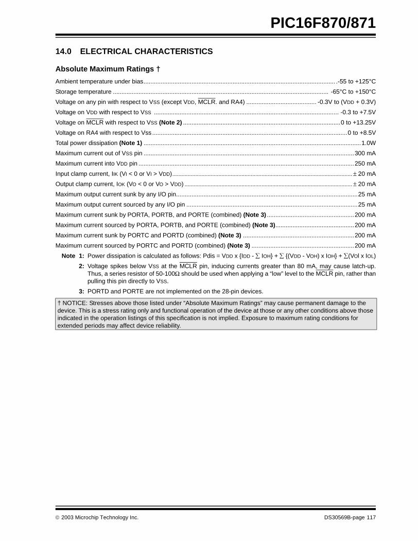
PIC16F870/871
14.0 ELECTRICAL CHARACTERISTICS
Absolute Maximum Ratings †
Ambient temperature under bias................................................................................................................ .-55 to +125°C
Storage temperature .............................................................................................................................. -65°C to +150°C
Voltage on any pin with respect to VSS (except VDD, MCLR. and RA4) ......................................... -0.3V to (VDD + 0.3V)
Voltage on VDD with respect to VSS ............................................................................................................ -0.3 to +7.5V
Voltage on MCLR with respect to VSS (Note 2) ............................................................................................0 to +13.25V
Voltage on RA4 with respect to Vss ..................................................................................................................0 to +8.5V
Total power dissipation (Note 1) ...............................................................................................................................1.0W
Maximum current out of VSS pin ...........................................................................................................................300 mA
Maximum current into VDD pin ..............................................................................................................................250 mA
Input clamp current, IIK (VI < 0 or VI > VDD)..................................................................................................................... ± 20 mA
Output clamp current, IOK (VO < 0 or VO > VDD) ............................................................................................................. ± 20 mA
Maximum output current sunk by any I/O pin..........................................................................................................25 mA
Maximum output current sourced by any I/O pin ....................................................................................................25 mA
Maximum current sunk by PORTA, PORTB, and PORTE (combined) (Note 3) ...................................................200 mA
Maximum current sourced by PORTA, PORTB, and PORTE (combined) (Note 3)..............................................200 mA
Maximum current sunk by PORTC and PORTD (combined) (Note 3) .................................................................200 mA
Maximum current sourced by PORTC and PORTD (combined) (Note 3) ............................................................200 mA
Note 1: Power dissipation is calculated as follows: Pdis = VDD x IDD - ∑ IOH + ∑ (VDD - VOH) x IOH + ∑(VOl x IOL)
2: Voltage spikes below VSS at the MCLR pin, inducing currents greater than 80 mA, may cause latch-up.Thus, a series resistor of 50-100Ω should be used when applying a “low” level to the MCLR pin, rather thanpulling this pin directly to VSS.
3: PORTD and PORTE are not implemented on the 28-pin devices.
† NOTICE: Stresses above those listed under “Absolute Maximum Ratings” may cause permanent damage to the device. This is a stress rating only and functional operation of the device at those or any other conditions above those indicated in the operation listings of this specification is not implied. Exposure to maximum rating conditions for extended periods may affect device reliability.
2003 Microchip Technology Inc. DS30569B-page 117
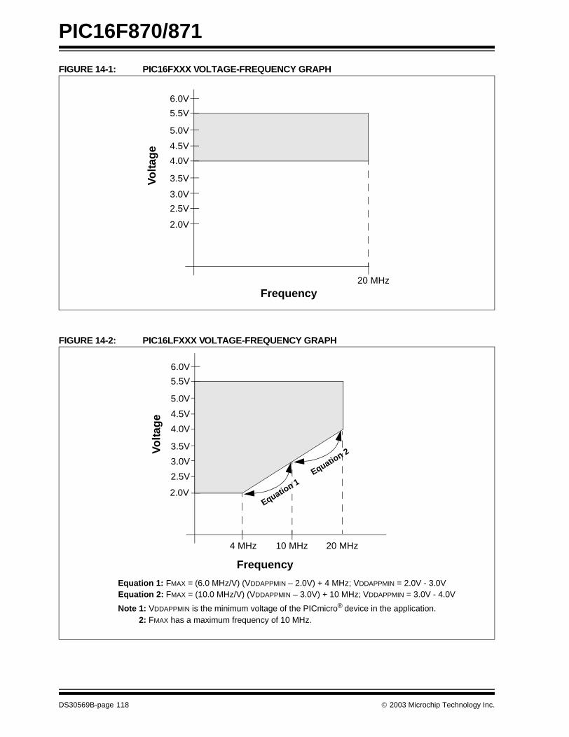
PIC16F870/871
FIGURE 14-1: PIC16FXXX VOLTAGE-FREQUENCY GRAPH
FIGURE 14-2: PIC16LFXXX VOLTAGE-FREQUENCY GRAPH
Frequency
Volta
ge
6.0V
5.5V
4.5V
4.0V
2.0V
20 MHz
5.0V
3.5V
3.0V
2.5V
Frequency
Vo
ltag
e
6.0V
5.5V
4.5V
4.0V
2.0V
5.0V
3.5V
3.0V
2.5V
Equation 1: FMAX = (6.0 MHz/V) (VDDAPPMIN – 2.0V) + 4 MHz; VDDAPPMIN = 2.0V - 3.0V
Note 1: VDDAPPMIN is the minimum voltage of the PICmicro® device in the application.
4 MHz 10 MHz
Note 2: FMAX has a maximum frequency of 10 MHz.
20 MHz
Equation 1
Equation 2
Equation 2: FMAX = (10.0 MHz/V) (VDDAPPMIN – 3.0V) + 10 MHz; VDDAPPMIN = 3.0V - 4.0V
DS30569B-page 118 2003 Microchip Technology Inc.
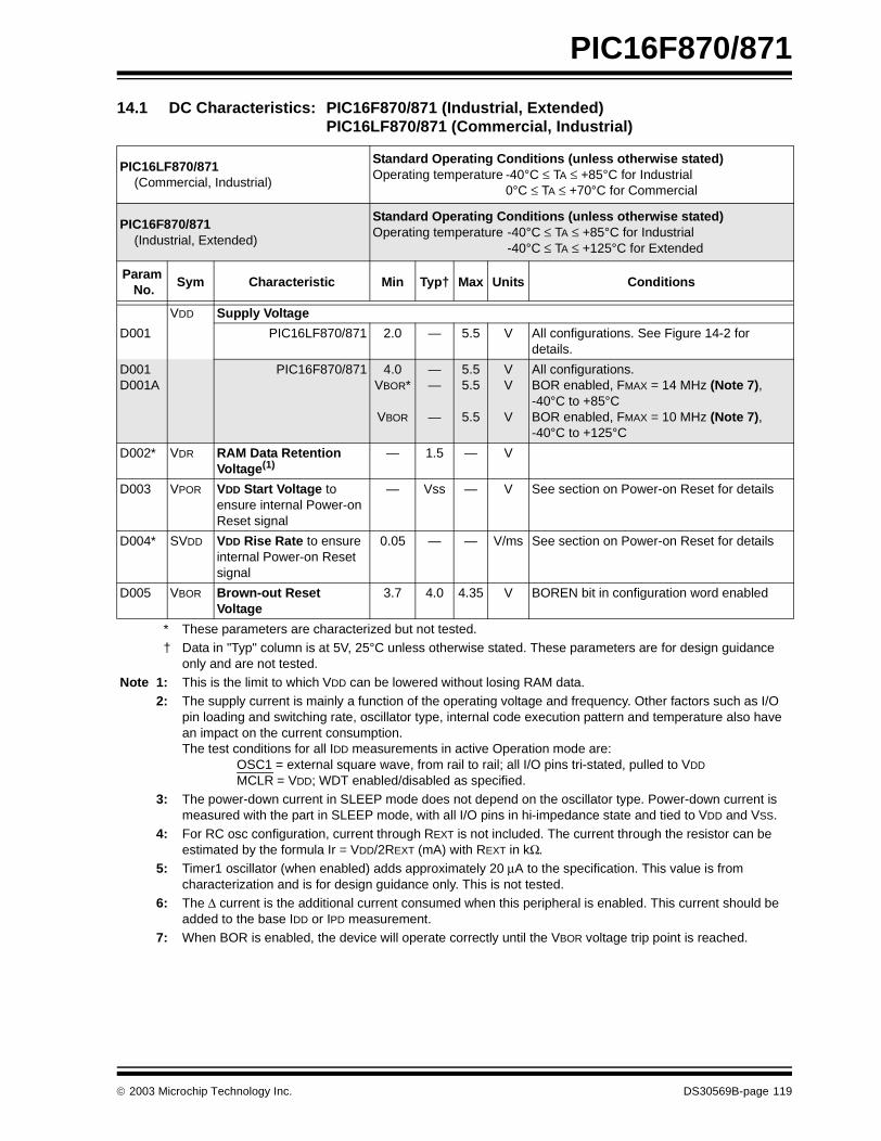
PIC16F870/871
14.1 DC Characteristics: PIC16F870/871 (Industrial, Extended)PIC16LF870/871 (Commercial, Industrial)
PIC16LF870/871 (Commercial, Industrial)
Standard Operating Conditions (unless otherwise stated)Operating temperature -40°C ≤ TA ≤ +85°C for Industrial
0°C ≤ TA ≤ +70°C for Commercial
PIC16F870/871 (Industrial, Extended)
Standard Operating Conditions (unless otherwise stated)Operating temperature -40°C ≤ TA ≤ +85°C for Industrial
-40°C ≤ TA ≤ +125°C for Extended
Param No.
Sym Characteristic Min Typ† Max Units Conditions
VDD Supply Voltage
D001 PIC16LF870/871 2.0 — 5.5 V All configurations. See Figure 14-2 for details.
D001D001A
PIC16F870/871 4.0VBOR*
VBOR
——
—
5.55.5
5.5
VV
V
All configurations.BOR enabled, FMAX = 14 MHz (Note 7), -40°C to +85°CBOR enabled, FMAX = 10 MHz (Note 7), -40°C to +125°C
D002* VDR RAM Data RetentionVoltage(1)
— 1.5 — V
D003 VPOR VDD Start Voltage toensure internal Power-on Reset signal
— Vss — V See section on Power-on Reset for details
D004* SVDD VDD Rise Rate to ensure internal Power-on Reset signal
0.05 — — V/ms See section on Power-on Reset for details
D005 VBOR Brown-out Reset Voltage
3.7 4.0 4.35 V BOREN bit in configuration word enabled
* These parameters are characterized but not tested.† Data in "Typ" column is at 5V, 25°C unless otherwise stated. These parameters are for design guidance
only and are not tested.Note 1: This is the limit to which VDD can be lowered without losing RAM data.
2: The supply current is mainly a function of the operating voltage and frequency. Other factors such as I/O pin loading and switching rate, oscillator type, internal code execution pattern and temperature also have an impact on the current consumption.The test conditions for all IDD measurements in active Operation mode are:
OSC1 = external square wave, from rail to rail; all I/O pins tri-stated, pulled to VDD MCLR = VDD; WDT enabled/disabled as specified.
3: The power-down current in SLEEP mode does not depend on the oscillator type. Power-down current is measured with the part in SLEEP mode, with all I/O pins in hi-impedance state and tied to VDD and VSS.
4: For RC osc configuration, current through REXT is not included. The current through the resistor can be estimated by the formula Ir = VDD/2REXT (mA) with REXT in kΩ.
5: Timer1 oscillator (when enabled) adds approximately 20 µA to the specification. This value is from characterization and is for design guidance only. This is not tested.
6: The ∆ current is the additional current consumed when this peripheral is enabled. This current should be added to the base IDD or IPD measurement.
7: When BOR is enabled, the device will operate correctly until the VBOR voltage trip point is reached.
2003 Microchip Technology Inc. DS30569B-page 119
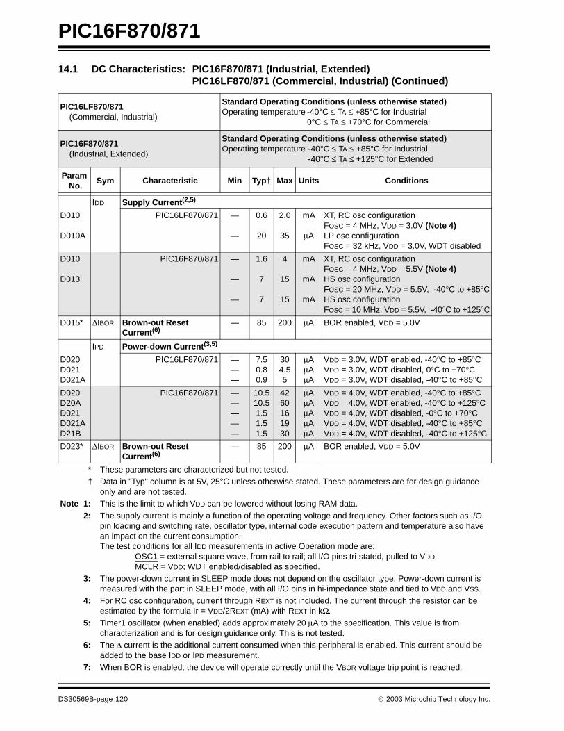
PIC16F870/871
IDD Supply Current(2,5)
D010
D010A
PIC16LF870/871 —
—
0.6
20
2.0
35
mA
µA
XT, RC osc configurationFOSC = 4 MHz, VDD = 3.0V (Note 4)LP osc configurationFOSC = 32 kHz, VDD = 3.0V, WDT disabled
D010
D013
PIC16F870/871 —
—
—
1.6
7
7
4
15
15
mA
mA
mA
XT, RC osc configuration FOSC = 4 MHz, VDD = 5.5V (Note 4)HS osc configuration FOSC = 20 MHz, VDD = 5.5V, -40°C to +85°CHS osc configuration FOSC = 10 MHz, VDD = 5.5V, -40°C to +125°C
D015* ∆IBOR Brown-out Reset Current(6)
— 85 200 µA BOR enabled, VDD = 5.0V
IPD Power-down Current(3,5)
D020D021D021A
PIC16LF870/871 ———
7.50.80.9
304.55
µAµAµA
VDD = 3.0V, WDT enabled, -40°C to +85°CVDD = 3.0V, WDT disabled, 0°C to +70°CVDD = 3.0V, WDT disabled, -40°C to +85°C
D020D20AD021D021AD21B
PIC16F870/871 —————
10.510.51.51.51.5
4260161930
µAµAµAµAµA
VDD = 4.0V, WDT enabled, -40°C to +85°CVDD = 4.0V, WDT enabled, -40°C to +125°CVDD = 4.0V, WDT disabled, -0°C to +70°CVDD = 4.0V, WDT disabled, -40°C to +85°CVDD = 4.0V, WDT disabled, -40°C to +125°C
D023* ∆IBOR Brown-out Reset Current(6)
— 85 200 µA BOR enabled, VDD = 5.0V
14.1 DC Characteristics: PIC16F870/871 (Industrial, Extended)PIC16LF870/871 (Commercial, Industrial) (Continued)
PIC16LF870/871 (Commercial, Industrial)
Standard Operating Conditions (unless otherwise stated)Operating temperature -40°C ≤ TA ≤ +85°C for Industrial
0°C ≤ TA ≤ +70°C for Commercial
PIC16F870/871 (Industrial, Extended)
Standard Operating Conditions (unless otherwise stated)Operating temperature -40°C ≤ TA ≤ +85°C for Industrial
-40°C ≤ TA ≤ +125°C for Extended
Param No.
Sym Characteristic Min Typ† Max Units Conditions
* These parameters are characterized but not tested.† Data in "Typ" column is at 5V, 25°C unless otherwise stated. These parameters are for design guidance
only and are not tested.Note 1: This is the limit to which VDD can be lowered without losing RAM data.
2: The supply current is mainly a function of the operating voltage and frequency. Other factors such as I/O pin loading and switching rate, oscillator type, internal code execution pattern and temperature also have an impact on the current consumption.The test conditions for all IDD measurements in active Operation mode are:
OSC1 = external square wave, from rail to rail; all I/O pins tri-stated, pulled to VDD MCLR = VDD; WDT enabled/disabled as specified.
3: The power-down current in SLEEP mode does not depend on the oscillator type. Power-down current is measured with the part in SLEEP mode, with all I/O pins in hi-impedance state and tied to VDD and VSS.
4: For RC osc configuration, current through REXT is not included. The current through the resistor can be estimated by the formula Ir = VDD/2REXT (mA) with REXT in kΩ.
5: Timer1 oscillator (when enabled) adds approximately 20 µA to the specification. This value is from characterization and is for design guidance only. This is not tested.
6: The ∆ current is the additional current consumed when this peripheral is enabled. This current should be added to the base IDD or IPD measurement.
7: When BOR is enabled, the device will operate correctly until the VBOR voltage trip point is reached.
DS30569B-page 120 2003 Microchip Technology Inc.
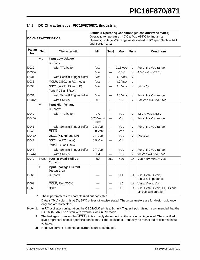
PIC16F870/871
14.2 DC Characteristics: PIC16F870/871 (Industrial)
DC CHARACTERISTICS
Standard Operating Conditions (unless otherwise stated)Operating temperature -40°C ≤ TA ≤ +85°C for IndustrialOperating voltage VDD range as described in DC spec Section 14.1 and Section 14.2.
ParamNo.
Sym Characteristic Min Typ† Max Units Conditions
VIL Input Low Voltage
I/O ports:
D030 with TTL buffer VSS — 0.15 VDD V For entire VDD range
D030A VSS — 0.8V V 4.5V ≤ VDD ≤ 5.5V
D031 with Schmitt Trigger buffer VSS — 0.2 VDD V
D032 MCLR, OSC1 (in RC mode) VSS — 0.2 VDD V
D033 OSC1 (in XT, HS and LP) VSS — 0.3 VDD V (Note 1)
Ports RC3 and RC4:
D034 with Schmitt Trigger buffer VSS — 0.3 VDD V For entire VDD range
D034A with SMBus -0.5 — 0.6 V For VDD = 4.5 to 5.5V
VIH Input High Voltage
I/O ports: —
D040 with TTL buffer 2.0 — VDD V 4.5V ≤ VDD ≤ 5.5V
D040A 0.25 VDD + 0.8V
— VDD V For entire VDD range
D041 with Schmitt Trigger buffer 0.8 VDD — VDD V For entire VDD range
D042 MCLR 0.8 VDD — VDD V
D042A OSC1 (XT, HS and LP) 0.7 VDD — VDD V (Note 1)
D043 OSC1 (in RC mode) 0.9 VDD — VDD V
Ports RC3 and RC4:
D044 with Schmitt Trigger buffer 0.7 VDD — VDD V For entire VDD range
D044A with SMBus 1.4 — 5.5 V for VDD = 4.5 to 5.5V
D070 IPURB PORTB Weak Pull-up Current
50 250 400 µA VDD = 5V, VPIN = VSS
IIL Input Leakage Current (Notes 2, 3)
D060 I/O ports — — ±1 µA Vss ≤ VPIN ≤ VDD, Pin at hi-impedance
D061 MCLR, RA4/T0CKI — — ±5 µA Vss ≤ VPIN ≤ VDD
D063 OSC1 — — ±5 µA Vss ≤ VPIN ≤ VDD, XT, HS and LP osc configuration
* These parameters are characterized but not tested.
† Data in "Typ" column is at 5V, 25°C unless otherwise stated. These parameters are for design guidanceonly and are not tested.
Note 1: In RC oscillator configuration, the OSC1/CLKI pin is a Schmitt Trigger input. It is not recommended that the PIC16F870/871 be driven with external clock in RC mode.
2: The leakage current on the MCLR pin is strongly dependent on the applied voltage level. The specified levels represent normal operating conditions. Higher leakage current may be measured at different input voltages.
3: Negative current is defined as current sourced by the pin.
2003 Microchip Technology Inc. DS30569B-page 121
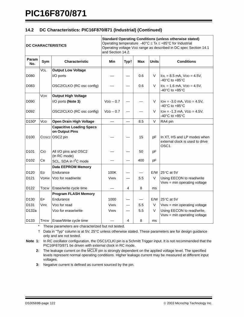
PIC16F870/871
VOL Output Low Voltage
D080 I/O ports — — 0.6 V IOL = 8.5 mA, VDD = 4.5V, -40°C to +85°C
D083 OSC2/CLKO (RC osc config) — — 0.6 V IOL = 1.6 mA, VDD = 4.5V, -40°C to +85°C
VOH Output High Voltage
D090 I/O ports (Note 3) VDD – 0.7 — — V IOH = -3.0 mA, VDD = 4.5V, -40°C to +85°C
D092 OSC2/CLKO (RC osc config) VDD – 0.7 — — V IOH = -1.3 mA, VDD = 4.5V, -40°C to +85°C
D150* VOD Open Drain High Voltage — — 8.5 V RA4 pin
Capacitive Loading Specs on Output Pins
D100 COSC2 OSC2 pin — — 15 pF In XT, HS and LP modes when external clock is used to drive OSC1.
D101
D102
CIO
CB
All I/O pins and OSC2 (in RC mode)
SCL, SDA in I2C mode
—
—
—
—
50
400
pF
pF
Data EEPROM Memory
D120 ED Endurance 100K — — E/W 25°C at 5V
D121 VDRW VDD for read/write VMIN — 5.5 V Using EECON to read/writeVMIN = min operating voltage
D122 TDEW Erase/write cycle time — 4 8 ms
Program FLASH Memory
D130 EP Endurance 1000 — — E/W 25°C at 5V
D131 VPR VDD for read VMIN — 5.5 V VMIN = min operating voltage
D132a VDD for erase/write VMIN — 5.5 V Using EECON to read/write, VMIN = min operating voltage
D133 TPEW Erase/Write cycle time — 4 8 ms
14.2 DC Characteristics: PIC16F870/871 (Industrial) (Continued)
DC CHARACTERISTICS
Standard Operating Conditions (unless otherwise stated)Operating temperature -40°C ≤ TA ≤ +85°C for IndustrialOperating voltage VDD range as described in DC spec Section 14.1 and Section 14.2.
ParamNo.
Sym Characteristic Min Typ† Max Units Conditions
* These parameters are characterized but not tested.† Data in "Typ" column is at 5V, 25°C unless otherwise stated. These parameters are for design guidance
only and are not tested.Note 1: In RC oscillator configuration, the OSC1/CLKI pin is a Schmitt Trigger input. It is not recommended that the
PIC16F870/871 be driven with external clock in RC mode.2: The leakage current on the MCLR pin is strongly dependent on the applied voltage level. The specified
levels represent normal operating conditions. Higher leakage current may be measured at different input voltages.
3: Negative current is defined as current sourced by the pin.
DS30569B-page 122 2003 Microchip Technology Inc.
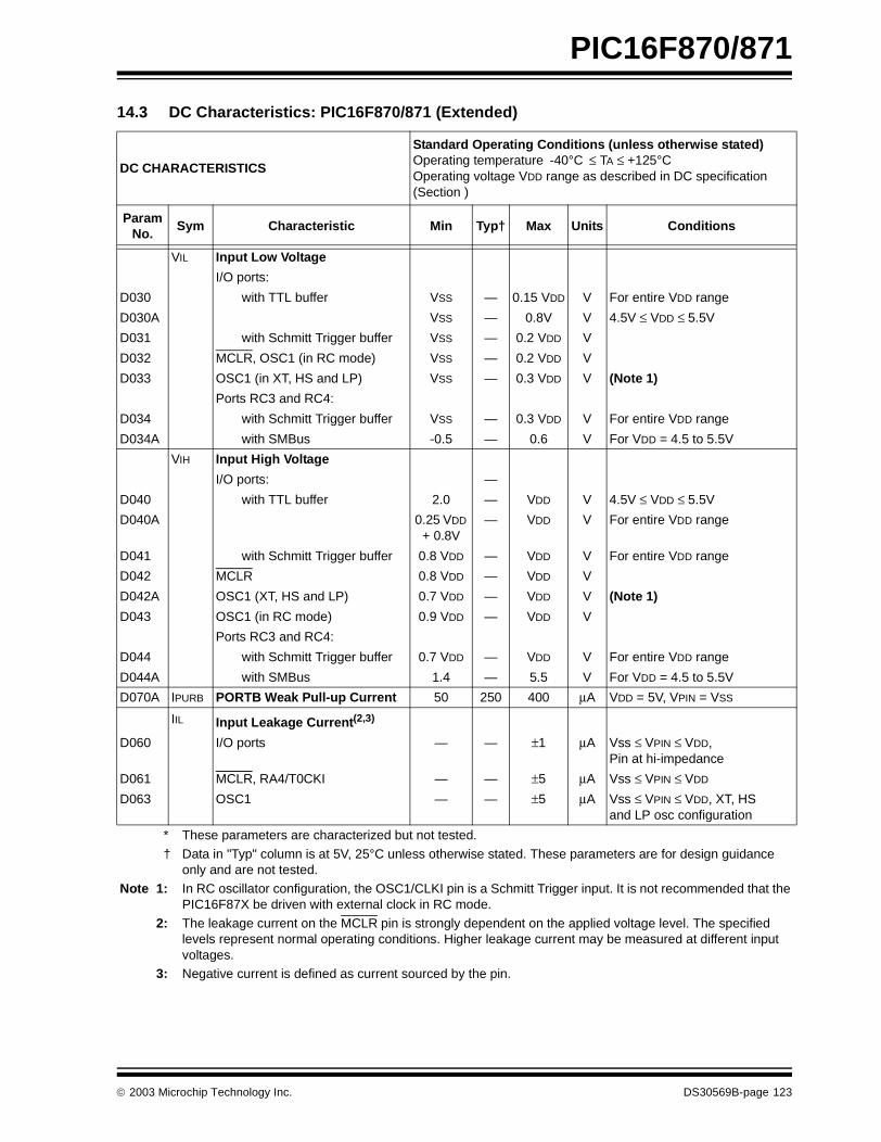
PIC16F870/871
14.3 DC Characteristics: PIC16F870/871 (Extended)
DC CHARACTERISTICS
Standard Operating Conditions (unless otherwise stated)Operating temperature -40°C ≤ TA ≤ +125°COperating voltage VDD range as described in DC specification (Section )
ParamNo.
Sym Characteristic Min Typ† Max Units Conditions
VIL Input Low Voltage
I/O ports:
D030 with TTL buffer VSS — 0.15 VDD V For entire VDD range
D030A VSS — 0.8V V 4.5V ≤ VDD ≤ 5.5V
D031 with Schmitt Trigger buffer VSS — 0.2 VDD V
D032 MCLR, OSC1 (in RC mode) VSS — 0.2 VDD V
D033 OSC1 (in XT, HS and LP) VSS — 0.3 VDD V (Note 1)
Ports RC3 and RC4:
D034 with Schmitt Trigger buffer VSS — 0.3 VDD V For entire VDD range
D034A with SMBus -0.5 — 0.6 V For VDD = 4.5 to 5.5V
VIH Input High Voltage
I/O ports: —
D040 with TTL buffer 2.0 — VDD V 4.5V ≤ VDD ≤ 5.5V
D040A 0.25 VDD + 0.8V
— VDD V For entire VDD range
D041 with Schmitt Trigger buffer 0.8 VDD — VDD V For entire VDD range
D042 MCLR 0.8 VDD — VDD V
D042A OSC1 (XT, HS and LP) 0.7 VDD — VDD V (Note 1)
D043 OSC1 (in RC mode) 0.9 VDD — VDD V
Ports RC3 and RC4:
D044 with Schmitt Trigger buffer 0.7 VDD — VDD V For entire VDD range
D044A with SMBus 1.4 — 5.5 V For VDD = 4.5 to 5.5V
D070A IPURB PORTB Weak Pull-up Current 50 250 400 µA VDD = 5V, VPIN = VSS
IIL Input Leakage Current(2,3)
D060 I/O ports — — ±1 µA Vss ≤ VPIN ≤ VDD, Pin at hi-impedance
D061 MCLR, RA4/T0CKI — — ±5 µA Vss ≤ VPIN ≤ VDD
D063 OSC1 — — ±5 µA Vss ≤ VPIN ≤ VDD, XT, HS and LP osc configuration
* These parameters are characterized but not tested.
† Data in "Typ" column is at 5V, 25°C unless otherwise stated. These parameters are for design guidanceonly and are not tested.
Note 1: In RC oscillator configuration, the OSC1/CLKI pin is a Schmitt Trigger input. It is not recommended that the PIC16F87X be driven with external clock in RC mode.
2: The leakage current on the MCLR pin is strongly dependent on the applied voltage level. The specified levels represent normal operating conditions. Higher leakage current may be measured at different input voltages.
3: Negative current is defined as current sourced by the pin.
2003 Microchip Technology Inc. DS30569B-page 123
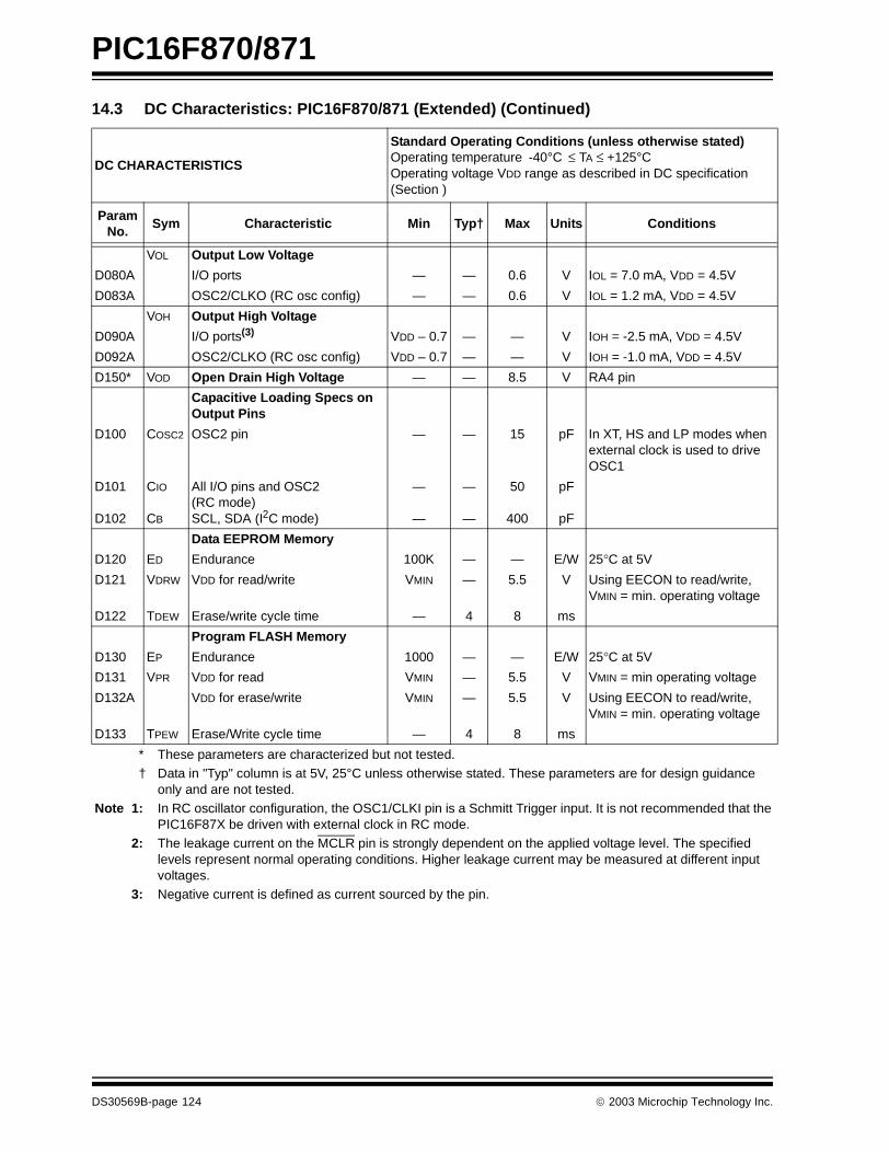
PIC16F870/871
VOL Output Low Voltage
D080A I/O ports — — 0.6 V IOL = 7.0 mA, VDD = 4.5V
D083A OSC2/CLKO (RC osc config) — — 0.6 V IOL = 1.2 mA, VDD = 4.5V
VOH Output High Voltage
D090A I/O ports(3) VDD – 0.7 — — V IOH = -2.5 mA, VDD = 4.5V
D092A OSC2/CLKO (RC osc config) VDD – 0.7 — — V IOH = -1.0 mA, VDD = 4.5V
D150* VOD Open Drain High Voltage — — 8.5 V RA4 pin
Capacitive Loading Specs on Output Pins
D100 COSC2 OSC2 pin — — 15 pF In XT, HS and LP modes when external clock is used to drive OSC1
D101
D102
CIO
CB
All I/O pins and OSC2 (RC mode) SCL, SDA (I2C mode)
—
—
—
—
50
400
pF
pF
Data EEPROM Memory
D120 ED Endurance 100K — — E/W 25°C at 5V
D121 VDRW VDD for read/write VMIN — 5.5 V Using EECON to read/write,VMIN = min. operating voltage
D122 TDEW Erase/write cycle time — 4 8 ms
Program FLASH Memory
D130 EP Endurance 1000 — — E/W 25°C at 5V
D131 VPR VDD for read VMIN — 5.5 V VMIN = min operating voltage
D132A VDD for erase/write VMIN — 5.5 V Using EECON to read/write, VMIN = min. operating voltage
D133 TPEW Erase/Write cycle time — 4 8 ms
14.3 DC Characteristics: PIC16F870/871 (Extended) (Continued)
DC CHARACTERISTICS
Standard Operating Conditions (unless otherwise stated)Operating temperature -40°C ≤ TA ≤ +125°COperating voltage VDD range as described in DC specification (Section )
ParamNo.
Sym Characteristic Min Typ† Max Units Conditions
* These parameters are characterized but not tested.† Data in "Typ" column is at 5V, 25°C unless otherwise stated. These parameters are for design guidance
only and are not tested.Note 1: In RC oscillator configuration, the OSC1/CLKI pin is a Schmitt Trigger input. It is not recommended that the
PIC16F87X be driven with external clock in RC mode.2: The leakage current on the MCLR pin is strongly dependent on the applied voltage level. The specified
levels represent normal operating conditions. Higher leakage current may be measured at different input voltages.
3: Negative current is defined as current sourced by the pin.
DS30569B-page 124 2003 Microchip Technology Inc.
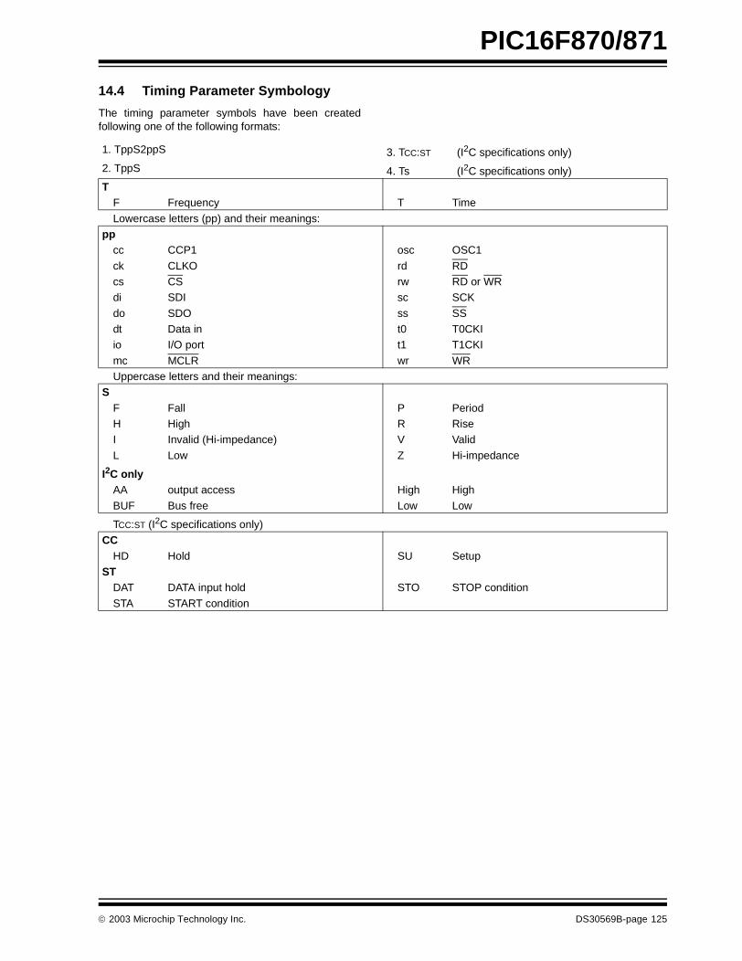
PIC16F870/871
14.4 Timing Parameter Symbology
The timing parameter symbols have been createdfollowing one of the following formats:
1. TppS2ppS 3. TCC:ST (I2C specifications only)
2. TppS 4. Ts (I2C specifications only)T
F Frequency T Time
Lowercase letters (pp) and their meanings:pp
cc CCP1 osc OSC1
ck CLKO rd RDcs CS rw RD or WRdi SDI sc SCK
do SDO ss SSdt Data in t0 T0CKIio I/O port t1 T1CKI
mc MCLR wr WRUppercase letters and their meanings:
SF Fall P PeriodH High R RiseI Invalid (Hi-impedance) V Valid
L Low Z Hi-impedance
I2C onlyAA output access High High
BUF Bus free Low Low
TCC:ST (I2C specifications only)CC
HD Hold SU SetupST
DAT DATA input hold STO STOP condition
STA START condition
2003 Microchip Technology Inc. DS30569B-page 125
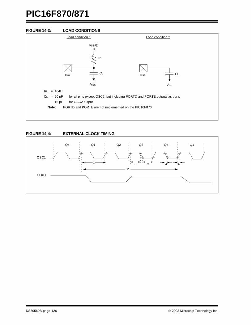
PIC16F870/871
FIGURE 14-3: LOAD CONDITIONS
FIGURE 14-4: EXTERNAL CLOCK TIMING
VDD/2
CL
RL
Pin Pin
VSS VSS
CL
RL = 464Ω
CL = 50 pF for all pins except OSC2, but including PORTD and PORTE outputs as ports
15 pF for OSC2 output
Note: PORTD and PORTE are not implemented on the PIC16F870.
Load condition 1 Load condition 2
OSC1
CLKO
Q4 Q1 Q2 Q3 Q4 Q1
1
2
3 3 4 4
DS30569B-page 126 2003 Microchip Technology Inc.
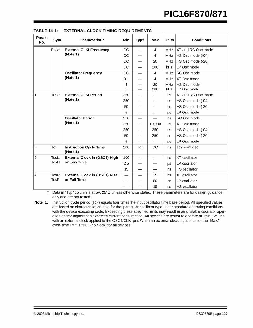
PIC16F870/871
TABLE 14-1: EXTERNAL CLOCK TIMING REQUIREMENTS
Param No.
Sym Characteristic Min Typ† Max Units Conditions
FOSC External CLKI Frequency (Note 1)
DC — 4 MHz XT and RC Osc mode
DC — 4 MHz HS Osc mode (-04)
DC — 20 MHz HS Osc mode (-20)
DC — 200 kHz LP Osc mode
Oscillator Frequency (Note 1)
DC — 4 MHz RC Osc mode
0.1 — 4 MHz XT Osc mode
45
——
20200
MHzkHz
HS Osc mode LP Osc mode
1 TOSC External CLKI Period(Note 1)
250 — — ns XT and RC Osc mode
250 — — ns HS Osc mode (-04)
50 — — ns HS Osc mode (-20)
5 — — µs LP Osc mode
Oscillator Period(Note 1)
250 — — ns RC Osc mode
250 — 10,000 ns XT Osc mode
250 — 250 ns HS Osc mode (-04)
50 — 250 ns HS Osc mode (-20)
5 — — µs LP Osc mode
2 TCY Instruction Cycle Time (Note 1)
200 TCY DC ns TCY = 4/FOSC
3 TosL,TosH
External Clock in (OSC1) High or Low Time
100 — — ns XT oscillator
2.5 — — µs LP oscillator
15 — — ns HS oscillator
4 TosR,TosF
External Clock in (OSC1) Rise or Fall Time
— — 25 ns XT oscillator
— — 50 ns LP oscillator
— — 15 ns HS oscillator
† Data in "Typ" column is at 5V, 25°C unless otherwise stated. These parameters are for design guidanceonly and are not tested.
Note 1: Instruction cycle period (TCY) equals four times the input oscillator time base period. All specified values are based on characterization data for that particular oscillator type under standard operating conditions with the device executing code. Exceeding these specified limits may result in an unstable oscillator oper-ation and/or higher than expected current consumption. All devices are tested to operate at "min." values with an external clock applied to the OSC1/CLKI pin. When an external clock input is used, the "Max." cycle time limit is "DC" (no clock) for all devices.
2003 Microchip Technology Inc. DS30569B-page 127
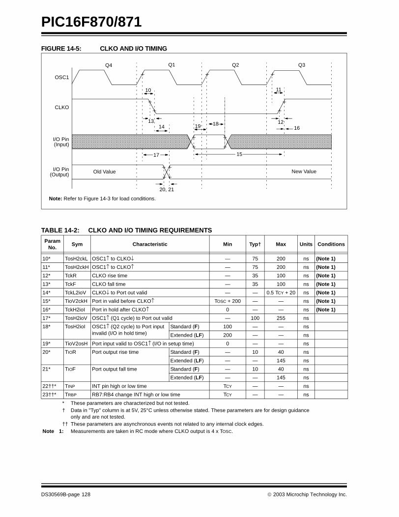
PIC16F870/871
FIGURE 14-5: CLKO AND I/O TIMING
TABLE 14-2: CLKO AND I/O TIMING REQUIREMENTS
Note: Refer to Figure 14-3 for load conditions.
OSC1
CLKO
I/O Pin(Input)
I/O Pin(Output)
Q4 Q1 Q2 Q3
10
1314
17
20, 21
19 18
15
11
1216
Old Value New Value
ParamNo.
Sym Characteristic Min Typ† Max Units Conditions
10* TosH2ckL OSC1↑ to CLKO↓ — 75 200 ns (Note 1)
11* TosH2ckH OSC1↑ to CLKO↑ — 75 200 ns (Note 1)
12* TckR CLKO rise time — 35 100 ns (Note 1)
13* TckF CLKO fall time — 35 100 ns (Note 1)
14* TckL2ioV CLKO↓ to Port out valid — — 0.5 TCY + 20 ns (Note 1)
15* TioV2ckH Port in valid before CLKO↑ TOSC + 200 — — ns (Note 1)
16* TckH2ioI Port in hold after CLKO↑ 0 — — ns (Note 1)
17* TosH2ioV OSC1↑ (Q1 cycle) to Port out valid — 100 255 ns
18* TosH2ioI OSC1↑ (Q2 cycle) to Port input invalid (I/O in hold time)
Standard (F) 100 — — ns
Extended (LF) 200 — — ns
19* TioV2osH Port input valid to OSC1↑ (I/O in setup time) 0 — — ns
20* TIOR Port output rise time Standard (F) — 10 40 ns
Extended (LF) — — 145 ns
21* TIOF Port output fall time Standard (F) — 10 40 ns
Extended (LF) — — 145 ns
22††* TINP INT pin high or low time TCY — — ns
23††* TRBP RB7:RB4 change INT high or low time TCY — — ns
* These parameters are characterized but not tested.† Data in "Typ" column is at 5V, 25°C unless otherwise stated. These parameters are for design guidance
only and are not tested.†† These parameters are asynchronous events not related to any internal clock edges.
Note 1: Measurements are taken in RC mode where CLKO output is 4 x TOSC.
DS30569B-page 128 2003 Microchip Technology Inc.
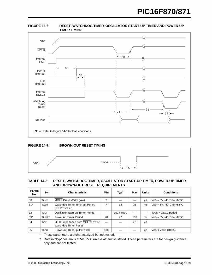
PIC16F870/871
FIGURE 14-6: RESET, WATCHDOG TIMER, OSCILLATOR START-UP TIMER AND POWER-UP TIMER TIMING
FIGURE 14-7: BROWN-OUT RESET TIMING
TABLE 14-3: RESET, WATCHDOG TIMER, OSCILLATOR START-UP TIMER, POWER-UP TIMER, AND BROWN-OUT RESET REQUIREMENTS
Param No.
Sym Characteristic Min Typ† Max Units Conditions
30 TmcL MCLR Pulse Width (low) 2 — — µs VDD = 5V, -40°C to +85°C
31* TWDT Watchdog Timer Time-out Period (No Prescaler)
7 18 33 ms VDD = 5V, -40°C to +85°C
32 TOST Oscillation Start-up Timer Period — 1024 TOSC — — TOSC = OSC1 period
33* TPWRT Power up Timer Period 28 72 132 ms VDD = 5V, -40°C to +85°C
34 TIOZ I/O Hi-impedance from MCLR Low or Watchdog Timer Reset
— — 2.1 µs
35 TBOR Brown-out Reset pulse width 100 — — µs VDD ≤ VBOR (D005)
* These parameters are characterized but not tested.† Data in "Typ" column is at 5V, 25°C unless otherwise stated. These parameters are for design guidance
only and are not tested.
VDD
MCLR
InternalPOR
PWRTTime-out
OscTime-out
InternalRESET
WatchdogTimerReset
33
32
30
3134
I/O Pins
34
Note: Refer to Figure 14-3 for load conditions.
VDD VBOR
35
2003 Microchip Technology Inc. DS30569B-page 129
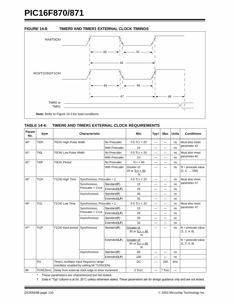
PIC16F870/871
FIGURE 14-8: TIMER0 AND TIMER1 EXTERNAL CLOCK TIMINGS
TABLE 14-4: TIMER0 AND TIMER1 EXTERNAL CLOCK REQUIREMENTS
Param No.
Sym Characteristic Min Typ† Max Units Conditions
40* Tt0H T0CKI High Pulse Width No Prescaler 0.5 TCY + 20 — — ns Must also meet parameter 42
With Prescaler 10 — — ns
41* Tt0L T0CKI Low Pulse Width No Prescaler 0.5 TCY + 20 — — ns Must also meet parameter 42 With Prescaler 10 — — ns
42* Tt0P T0CKI Period No Prescaler TCY + 40 — — ns
With Prescaler Greater of:20 or TCY + 40 N
— — ns N = prescale value (2, 4, ..., 256)
45* Tt1H T1CKI High Time Synchronous, Prescaler = 1 0.5 TCY + 20 — — ns Must also meet parameter 47 Synchronous,
Prescaler = 2,4,8Standard(F) 15 — — ns
Extended(LF) 25 — — ns
Asynchronous Standard(F) 30 — — ns
Extended(LF) 50 — — ns
46* Tt1L T1CKI Low Time Synchronous, Prescaler = 1 0.5 TCY + 20 — — ns Must also meet parameter 47 Synchronous,
Prescaler = 2,4,8Standard(F) 15 — — ns
Extended(LF) 25 — — ns
Asynchronous Standard(F) 30 — — ns
Extended(LF) 50 — — ns
47* Tt1P T1CKI input period Synchronous Standard(F) Greater of:30 or TCY + 40
N
— — ns N = prescale value (1, 2, 4, 8)
Extended(LF) Greater of:50 or TCY + 40
N
N = prescale value (1, 2, 4, 8)
Asynchronous Standard(F) 60 — — ns
Extended(LF) 100 — — ns
Ft1 Timer1 oscillator input frequency range (oscillator enabled by setting bit T1OSCEN)
DC — 200 kHz
48 TCKEZtmr1 Delay from external clock edge to timer increment 2 TOSC — 7 TOSC —
* These parameters are characterized but not tested.† Data in "Typ" column is at 5V, 25°C unless otherwise stated. These parameters are for design guidance only and are not tested.
Note: Refer to Figure 14-3 for load conditions.
46
47
45
48
41
42
40
RA4/T0CKI
RC0/T1OSO/T1CKI
TMR0 orTMR1
DS30569B-page 130 2003 Microchip Technology Inc.
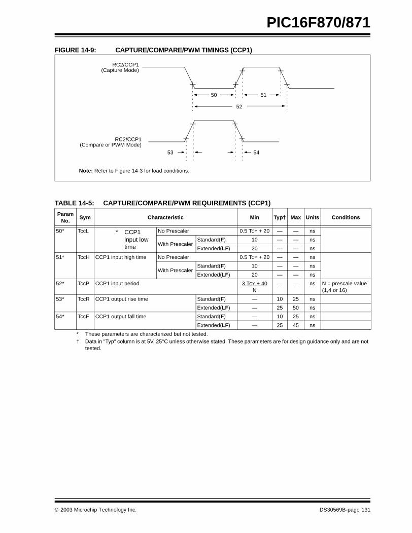
PIC16F870/871
FIGURE 14-9: CAPTURE/COMPARE/PWM TIMINGS (CCP1)
TABLE 14-5: CAPTURE/COMPARE/PWM REQUIREMENTS (CCP1)
Note: Refer to Figure 14-3 for load conditions.
RC2/CCP1(Capture Mode)
50 51
52
53 54
RC2/CCP1(Compare or PWM Mode)
Param No.
Sym Characteristic Min Typ† Max Units Conditions
50* TccL * CCP1 input low time
No Prescaler 0.5 TCY + 20 — — ns
With PrescalerStandard(F) 10 — — ns
Extended(LF) 20 — — ns
51* TccH CCP1 input high time No Prescaler 0.5 TCY + 20 — — ns
With PrescalerStandard(F) 10 — — ns
Extended(LF) 20 — — ns
52* TccP CCP1 input period 3 TCY + 40N
— — ns N = prescale value (1,4 or 16)
53* TccR CCP1 output rise time Standard(F) — 10 25 ns
Extended(LF) — 25 50 ns
54* TccF CCP1 output fall time Standard(F) — 10 25 ns
Extended(LF) — 25 45 ns
* These parameters are characterized but not tested.† Data in "Typ" column is at 5V, 25°C unless otherwise stated. These parameters are for design guidance only and are not
tested.
2003 Microchip Technology Inc. DS30569B-page 131

PIC16F870/871
FIGURE 14-10: PARALLEL SLAVE PORT TIMING (PIC16F871 ONLY)
TABLE 14-6: PARALLEL SLAVE PORT REQUIREMENTS (PIC16F871 ONLY)
Note: Refer to Figure 14-3 for load conditions.
RE2/CS
RE0/RD
RE1/WR
RD7:RD0
62
63
64
65
ParamNo.
Sym Characteristic Min Typ† Max Units Conditions
62 TdtV2wrH Data in valid before WR↑ or CS↑ (setup time) 2025
——
——
nsns Extended range only
63* TwrH2dtI WR↑ or CS↑ to data–in invalid (hold time) Standard(F) 20 — — ns
Extended(LF) 35 — — ns
64 TrdL2dtV RD↓ and CS↓ to data–out valid ——
——
8090
nsns Extended range only
65 TrdH2dtI RD↑ or CS↓ to data–out invalid 10 — 30 ns
* These parameters are characterized but not tested.† Data in "Typ" column is at 5V, 25°C unless otherwise stated. These parameters are for design guidance only and are not
tested.
DS30569B-page 132 2003 Microchip Technology Inc.
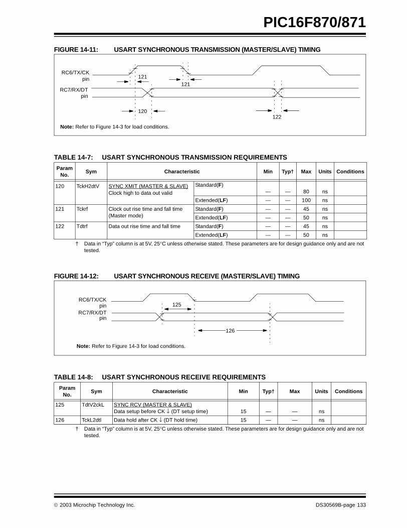
PIC16F870/871
FIGURE 14-11: USART SYNCHRONOUS TRANSMISSION (MASTER/SLAVE) TIMING
TABLE 14-7: USART SYNCHRONOUS TRANSMISSION REQUIREMENTS
FIGURE 14-12: USART SYNCHRONOUS RECEIVE (MASTER/SLAVE) TIMING
TABLE 14-8: USART SYNCHRONOUS RECEIVE REQUIREMENTS
Note: Refer to Figure 14-3 for load conditions.
121121
122
RC6/TX/CK
RC7/RX/DTpin
pin
120
ParamNo.
Sym Characteristic Min Typ† Max Units Conditions
120 TckH2dtV SYNC XMIT (MASTER & SLAVE)Clock high to data out valid
Standard(F)— — 80 ns
Extended(LF) — — 100 ns
121 Tckrf Clock out rise time and fall time (Master mode)
Standard(F) — — 45 ns
Extended(LF) — — 50 ns
122 Tdtrf Data out rise time and fall time Standard(F) — — 45 ns
Extended(LF) — — 50 ns
† Data in “Typ” column is at 5V, 25°C unless otherwise stated. These parameters are for design guidance only and are not tested.
Note: Refer to Figure 14-3 for load conditions.
125
126
RC6/TX/CK
RC7/RX/DTpin
pin
ParamNo.
Sym Characteristic Min Typ† Max Units Conditions
125 TdtV2ckL SYNC RCV (MASTER & SLAVE)Data setup before CK ↓ (DT setup time) 15 — — ns
126 TckL2dtl Data hold after CK ↓ (DT hold time) 15 — — ns
† Data in “Typ” column is at 5V, 25°C unless otherwise stated. These parameters are for design guidance only and are not tested.
2003 Microchip Technology Inc. DS30569B-page 133
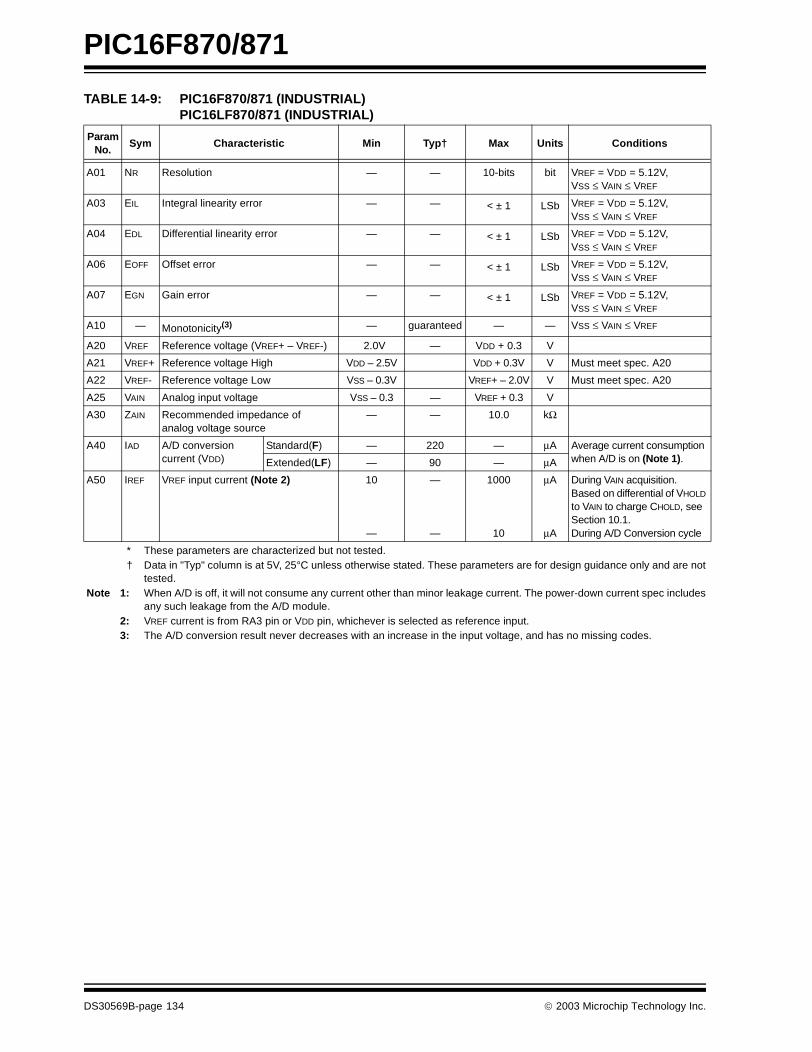
PIC16F870/871
TABLE 14-9: PIC16F870/871 (INDUSTRIAL)PIC16LF870/871 (INDUSTRIAL)
ParamNo.
Sym Characteristic Min Typ† Max Units Conditions
A01 NR Resolution — — 10-bits bit VREF = VDD = 5.12V, VSS ≤ VAIN ≤ VREF
A03 EIL Integral linearity error — — < ± 1 LSb VREF = VDD = 5.12V, VSS ≤ VAIN ≤ VREF
A04 EDL Differential linearity error — — < ± 1 LSb VREF = VDD = 5.12V, VSS ≤ VAIN ≤ VREF
A06 EOFF Offset error — — < ± 1 LSb VREF = VDD = 5.12V, VSS ≤ VAIN ≤ VREF
A07 EGN Gain error — — < ± 1 LSb VREF = VDD = 5.12V, VSS ≤ VAIN ≤ VREF
A10 — Monotonicity(3) — guaranteed — — VSS ≤ VAIN ≤ VREF
A20 VREF Reference voltage (VREF+ – VREF-) 2.0V — VDD + 0.3 V
A21 VREF+ Reference voltage High VDD – 2.5V VDD + 0.3V V Must meet spec. A20
A22 VREF- Reference voltage Low VSS – 0.3V VREF+ – 2.0V V Must meet spec. A20
A25 VAIN Analog input voltage VSS – 0.3 — VREF + 0.3 V
A30 ZAIN Recommended impedance of analog voltage source
— — 10.0 kΩ
A40 IAD A/D conversion current (VDD)
Standard(F) — 220 — µA Average current consumption when A/D is on (Note 1).Extended(LF) — 90 — µA
A50 IREF VREF input current (Note 2) 10
—
—
—
1000
10
µA
µA
During VAIN acquisition.Based on differential of VHOLD to VAIN to charge CHOLD, see Section 10.1.During A/D Conversion cycle
* These parameters are characterized but not tested.† Data in "Typ" column is at 5V, 25°C unless otherwise stated. These parameters are for design guidance only and are not
tested.Note 1: When A/D is off, it will not consume any current other than minor leakage current. The power-down current spec includes
any such leakage from the A/D module.2: VREF current is from RA3 pin or VDD pin, whichever is selected as reference input.3: The A/D conversion result never decreases with an increase in the input voltage, and has no missing codes.
DS30569B-page 134 2003 Microchip Technology Inc.
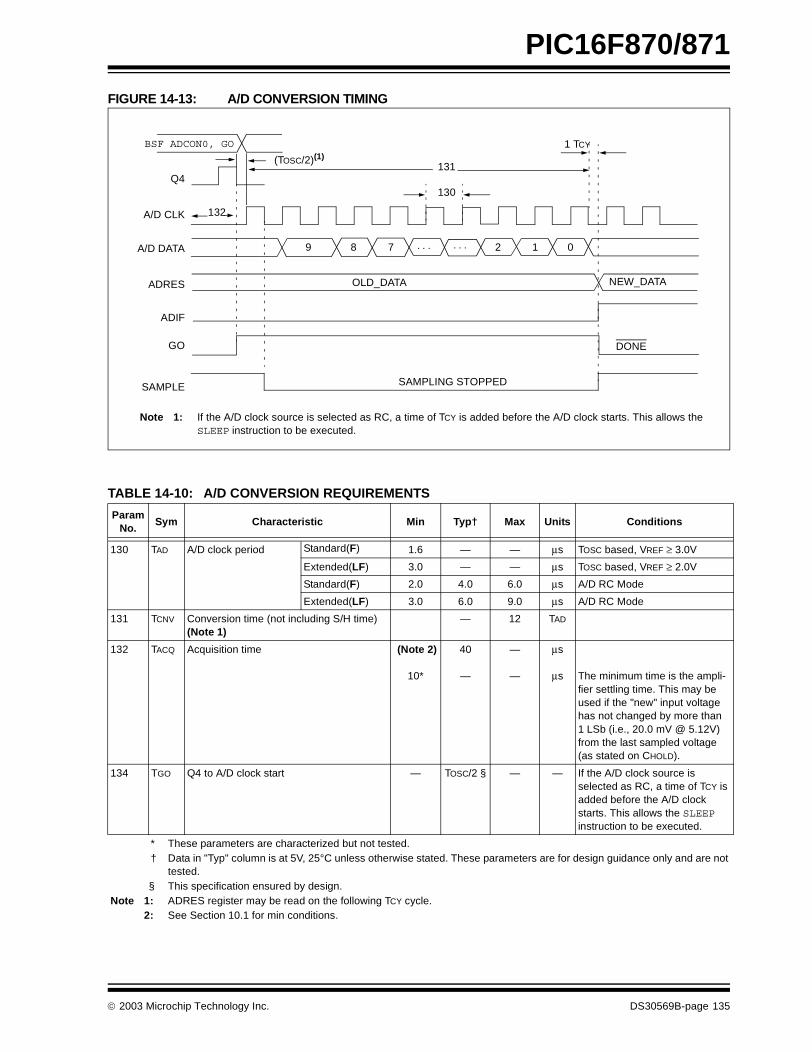
PIC16F870/871
FIGURE 14-13: A/D CONVERSION TIMING
TABLE 14-10: A/D CONVERSION REQUIREMENTS
131
130
132
BSF ADCON0, GO
Q4
A/D CLK
A/D DATA
ADRES
ADIF
GO
SAMPLE
OLD_DATA
SAMPLING STOPPED
DONE
NEW_DATA
(TOSC/2)(1)
9 8 7 2 1 0
Note 1: If the A/D clock source is selected as RC, a time of TCY is added before the A/D clock starts. This allows the SLEEP instruction to be executed.
1 TCY
. . . . . .
Param No.
Sym Characteristic Min Typ† Max Units Conditions
130 TAD A/D clock period Standard(F) 1.6 — — µs TOSC based, VREF ≥ 3.0V
Extended(LF) 3.0 — — µs TOSC based, VREF ≥ 2.0V
Standard(F) 2.0 4.0 6.0 µs A/D RC Mode
Extended(LF) 3.0 6.0 9.0 µs A/D RC Mode
131 TCNV Conversion time (not including S/H time) (Note 1)
— 12 TAD
132 TACQ Acquisition time (Note 2)
10*
40
—
—
—
µs
µs The minimum time is the ampli-fier settling time. This may be used if the "new" input voltage has not changed by more than 1 LSb (i.e., 20.0 mV @ 5.12V) from the last sampled voltage (as stated on CHOLD).
134 TGO Q4 to A/D clock start — TOSC/2 § — — If the A/D clock source is selected as RC, a time of TCY is added before the A/D clock starts. This allows the SLEEP instruction to be executed.
* These parameters are characterized but not tested.† Data in "Typ" column is at 5V, 25°C unless otherwise stated. These parameters are for design guidance only and are not
tested.§ This specification ensured by design.
Note 1: ADRES register may be read on the following TCY cycle.2: See Section 10.1 for min conditions.
2003 Microchip Technology Inc. DS30569B-page 135

PIC16F870/871
NOTES:
DS30569B-page 136 2003 Microchip Technology Inc.
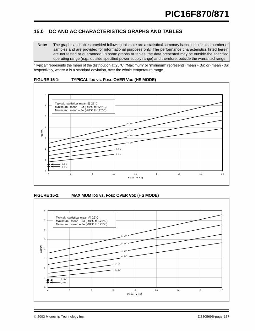
PIC16F870/871
15.0 DC AND AC CHARACTERISTICS GRAPHS AND TABLES
“Typical” represents the mean of the distribution at 25°C. “Maximum” or “minimum” represents (mean + 3σ) or (mean - 3σ)respectively, where σ is a standard deviation, over the whole temperature range.
FIGURE 15-1: TYPICAL IDD vs. FOSC OVER VDD (HS MODE)
FIGURE 15-2: MAXIMUM IDD vs. FOSC OVER VDD (HS MODE)
Note: The graphs and tables provided following this note are a statistical summary based on a limited number ofsamples and are provided for informational purposes only. The performance characteristics listed hereinare not tested or guaranteed. In some graphs or tables, the data presented may be outside the specifiedoperating range (e.g., outside specified power supply range) and therefore, outside the warranted range.
0
1
2
3
4
5
6
7
4 6 8 10 12 14 16 18 20
F O S C (M H z )
I DD
(mA
)
2 .5 V
2 .0 V
5 .5V
5 .0V
4 .5V
4 .0V
3 .5V
3 .0V
Typical: statistical mean @ 25°CMaximum: mean + 3σ (-40°C to 125°C) Minimum: mean – 3σ (-40°C to 125°C)
0
1
2
3
4
5
6
7
8
4 6 8 10 12 1 4 16 1 8 20
F O S C (M H z )
I DD
(mA
)
5 .5V
5 .0V
4 .5V
4 .0V
3 .5V
3 .0V
2 .5V
2 .0V
Typical: statistical mean @ 25°CMaximum: mean + 3σ (-40°C to 125°C) Minimum: mean – 3σ (-40°C to 125°C)
2003 Microchip Technology Inc. DS30569B-page 137

PIC16F870/871
FIGURE 15-3: TYPICAL IDD vs. FOSC OVER VDD (XT MODE)
FIGURE 15-4: MAXIMUM IDD vs. FOSC OVER VDD (LP MODE)
0.0
0.2
0.4
0.6
0.8
1.0
1.2
1.4
1.6
0.0 0.5 1.0 1.5 2.0 2.5 3.0 3.5 4.0
FOSC (MHz)
IDD
(mA
)
5.5V
5.0V
4.5V
4.0V
3.5V
2.5V
2.0V
3.0V
Typical: statistical mean @ 25°CMaximum: mean + 3σ (-40°C to 125°C) Minimum: mean – 3σ (-40°C to 125°C)
0.0
0.2
0.4
0.6
0.8
1.0
1.2
1.4
1.6
1.8
2.0
0.0 0.5 1.0 1.5 2.0 2.5 3.0 3.5 4.0
FOSC (MHz)
IDD
(mA
)
5.5V
5.0V
4.5V
4.0V
3.5V
2.5V
2.0V
3.0V
Typical: statistical mean @ 25°CMaximum: mean + 3σ (-40°C to 125°C) Minimum: mean – 3σ (-40°C to 125°C)
DS30569B-page 138 2003 Microchip Technology Inc.
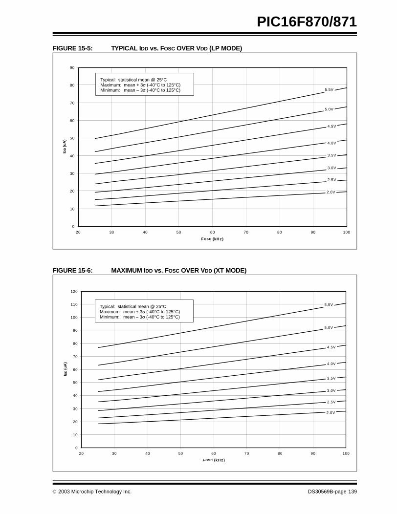
PIC16F870/871
FIGURE 15-5: TYPICAL IDD vs. FOSC OVER VDD (LP MODE)
FIGURE 15-6: MAXIMUM IDD vs. FOSC OVER VDD (XT MODE)
0
10
20
30
40
50
60
70
80
90
20 30 40 50 60 70 80 90 100
FOSC (kHz)
I DD (
uA
)
5.5V
5.0V
4.5V
4.0V
3.5V
3.0V
2.5V
2.0V
Typical: statistical mean @ 25°CMaximum: mean + 3σ (-40°C to 125°C) Minimum: mean – 3σ (-40°C to 125°C)
0
10
20
30
40
50
60
70
80
90
100
110
120
20 30 40 50 60 70 80 90 100
FOSC (kHz)
I DD (
uA
)
5.5V
5.0V
4.5V
4.0V
3.5V
3.0V
2.5V
2.0V
Typical: statistical mean @ 25°CMaximum: mean + 3σ (-40°C to 125°C) Minimum: mean – 3σ (-40°C to 125°C)
2003 Microchip Technology Inc. DS30569B-page 139
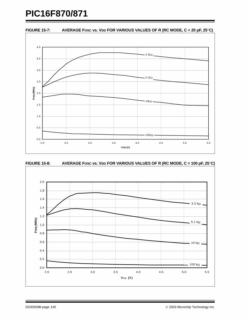
PIC16F870/871
FIGURE 15-7: AVERAGE FOSC vs. VDD FOR VARIOUS VALUES OF R (RC MODE, C = 20 pF, 25°C)
FIGURE 15-8: AVERAGE FOSC vs. VDD FOR VARIOUS VALUES OF R (RC MODE, C = 100 pF, 25°C)
0.0
0.5
1.0
1.5
2.0
2.5
3.0
3.5
4.0
2.0 2.5 3.0 3.5 4.0 4.5 5.0 5.5
VDD (V)
Fre
q (
MH
z)
3.3kΩ
5.1kΩ
10kΩ
100kΩ
0.0
0.2
0.4
0.6
0.8
1.0
1.2
1.4
1.6
1.8
2.0
2.0 2.5 3.0 3.5 4.0 4.5 5.0 5.5
V D D (V )
Fre
q (
MH
z)
3.3 kΩ
5.1 kΩ
10 kΩ
100 kΩ
DS30569B-page 140 2003 Microchip Technology Inc.
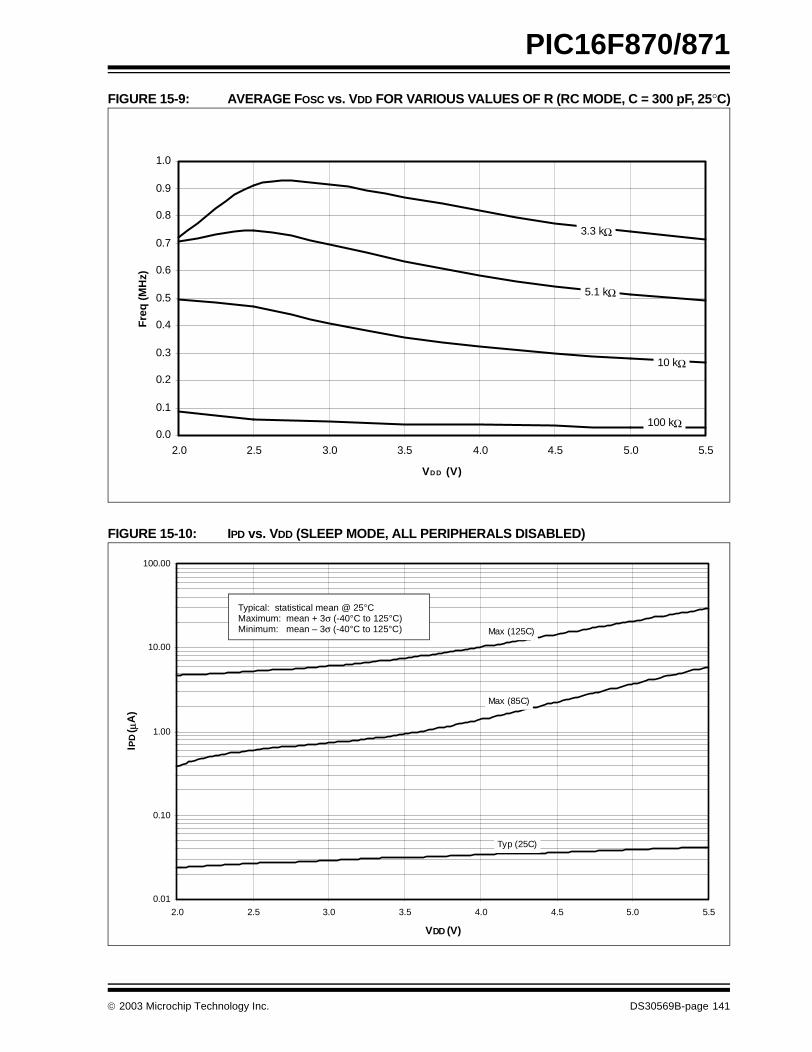
PIC16F870/871
FIGURE 15-9: AVERAGE FOSC vs. VDD FOR VARIOUS VALUES OF R (RC MODE, C = 300 pF, 25°C)
FIGURE 15-10: IPD vs. VDD (SLEEP MODE, ALL PERIPHERALS DISABLED)
0.0
0.1
0.2
0.3
0.4
0.5
0.6
0.7
0.8
0.9
1.0
2.0 2.5 3.0 3.5 4.0 4.5 5.0 5.5
VD D (V)
Fre
q (
MH
z)
3.3 kΩ
5.1 kΩ
10 kΩ
100 kΩ
0.01
0.10
1.00
10.00
100.00
2.0 2.5 3.0 3.5 4.0 4.5 5.0 5.5
VDD (V)
IPD
( µA
)
Max (125C)
Max (85C)
Typ (25C)
Typical: statistical mean @ 25°CMaximum: mean + 3σ (-40°C to 125°C) Minimum: mean – 3σ (-40°C to 125°C)
2003 Microchip Technology Inc. DS30569B-page 141
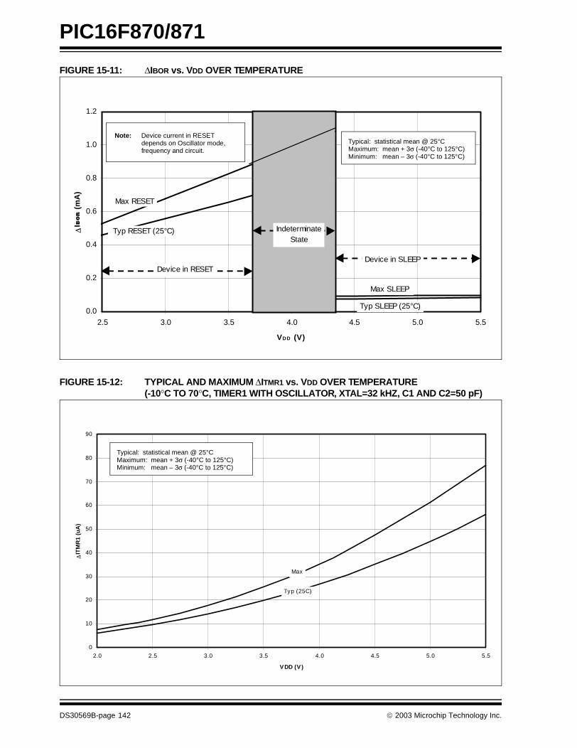
PIC16F870/871
FIGURE 15-11: ∆IBOR vs. VDD OVER TEMPERATURE
FIGURE 15-12: TYPICAL AND MAXIMUM ∆ITMR1 vs. VDD OVER TEMPERATURE (-10°C TO 70°C, TIMER1 WITH OSCILLATOR, XTAL=32 kHZ, C1 AND C2=50 pF)
0.0
0.2
0.4
0.6
0.8
1.0
1.2
2.5 3.0 3.5 4.0 4.5 5.0 5.5
VDD (V)
∆I
(m
A)
Device in SLEEPDevice in RESET
Max RESET
Typ RESET (25°C)
Max SLEEP
Typ SLEEP (25°C)
IndeterminateState
Typical: statistical mean @ 25°CMaximum: mean + 3σ (-40°C to 125°C) Minimum: mean – 3σ (-40°C to 125°C)
Note: Device current in RESET depends on Oscillator mode, frequency and circuit.
0
10
20
30
40
50
60
70
80
90
2.0 2.5 3.0 3.5 4.0 4.5 5.0 5.5
VDD (V )
∆IT
MR
1 (u
A)
Typ (25C)
Max
Typical: statistical mean @ 25°CMaximum: mean + 3σ (-40°C to 125°C) Minimum: mean – 3σ (-40°C to 125°C)
DS30569B-page 142 2003 Microchip Technology Inc.
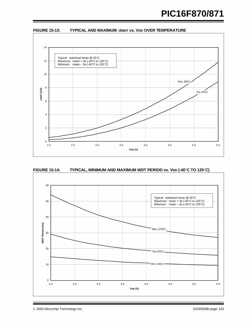
PIC16F870/871
FIGURE 15-13: TYPICAL AND MAXIMUM ∆IWDT vs. VDD OVER TEMPERATURE
FIGURE 15-14: TYPICAL, MINIMUM AND MAXIMUM WDT PERIOD vs. VDD (-40°C TO 125°C)
0
2
4
6
8
10
12
14
2.0 2.5 3.0 3.5 4.0 4.5 5.0 5.5
VDD (V)
∆I W
DT
(uA
)
Typ (25C)
Max (85C)
Typical: statistical mean @ 25°CMaximum: mean + 3σ (-40°C to 125°C) Minimum: mean – 3σ (-40°C to 125°C)
0
10
20
30
40
50
60
2.0 2.5 3.0 3.5 4.0 4.5 5.0 5.5
VDD (V)
WD
T P
erio
d (
ms)
Min (-40C)
Typ (25C)
Max (125C)
Typical: statistical mean @ 25°CMaximum: mean + 3σ (-40°C to 125°C) Minimum: mean – 3σ (-40°C to 125°C)
2003 Microchip Technology Inc. DS30569B-page 143

PIC16F870/871
FIGURE 15-15: AVERAGE WDT PERIOD vs. VDD OVER TEMPERATURE (-40°C TO 125°C)
FIGURE 15-16: TYPICAL, MINIMUM AND MAXIMUM VOH vs. IOH (VDD = 5V, -40°C TO 125°C)
0
5
10
15
20
25
30
35
40
45
50
2.0 2.5 3.0 3.5 4.0 4.5 5.0 5.5
VDD (V)
WD
T P
erio
d (
ms)
85C
125C
25C
-40C
Typical: statistical mean @ 25°CMaximum: mean + 3σ (-40°C to 125°C) Minimum: mean – 3σ (-40°C to 125°C)
2.0
2.5
3.0
3.5
4.0
4.5
5.0
0 5 10 15 20 25
IOH (-mA)
VO
H (V
)
Max (-40C)
Typ (25C)
Min (125C)
Typical: statistical mean @ 25°CMaximum: mean + 3σ (-40°C to 125°C) Minimum: mean – 3σ (-40°C to 125°C)
DS30569B-page 144 2003 Microchip Technology Inc.
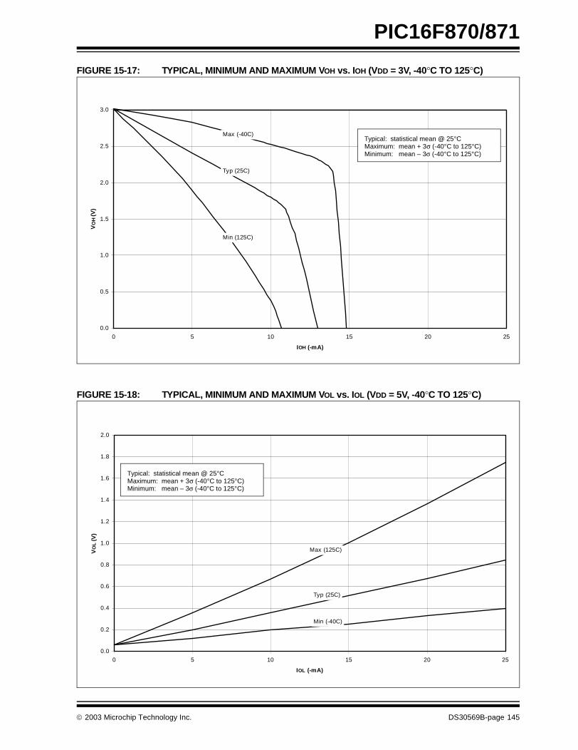
PIC16F870/871
FIGURE 15-17: TYPICAL, MINIMUM AND MAXIMUM VOH vs. IOH (VDD = 3V, -40°C TO 125°C)
FIGURE 15-18: TYPICAL, MINIMUM AND MAXIMUM VOL vs. IOL (VDD = 5V, -40°C TO 125°C)
0.0
0.5
1.0
1.5
2.0
2.5
3.0
0 5 10 15 20 25
IOH (-mA)
VO
H (
V)
Max (-40C)
Typ (25C)
Min (125C)
Typical: statistical mean @ 25°CMaximum: mean + 3σ (-40°C to 125°C) Minimum: mean – 3σ (-40°C to 125°C)
0.0
0.2
0.4
0.6
0.8
1.0
1.2
1.4
1.6
1.8
2.0
0 5 10 15 20 25
IOL (-mA)
VO
L (V
)
Max (125C)
Typ (25C)
Min (-40C)
Typical: statistical mean @ 25°CMaximum: mean + 3σ (-40°C to 125°C) Minimum: mean – 3σ (-40°C to 125°C)
2003 Microchip Technology Inc. DS30569B-page 145
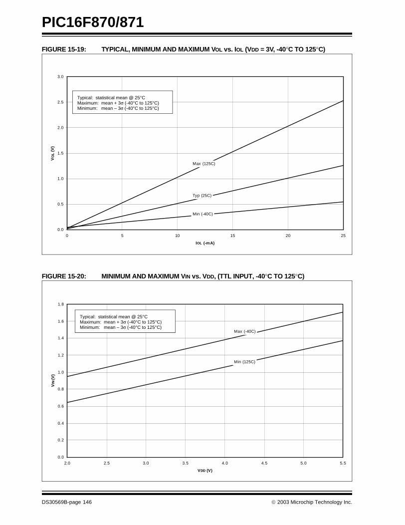
PIC16F870/871
FIGURE 15-19: TYPICAL, MINIMUM AND MAXIMUM VOL vs. IOL (VDD = 3V, -40°C TO 125°C)
FIGURE 15-20: MINIMUM AND MAXIMUM VIN vs. VDD, (TTL INPUT, -40°C TO 125°C)
0.0
0.5
1.0
1.5
2.0
2.5
3.0
0 5 10 15 20 25
IOL (-mA)
VO
L (V
)
Max (125C)
Typ (25C)
Min (-40C)
Typical: statistical mean @ 25°CMaximum: mean + 3σ (-40°C to 125°C) Minimum: mean – 3σ (-40°C to 125°C)
0.0
0.2
0.4
0.6
0.8
1.0
1.2
1.4
1.6
1.8
2.0 2.5 3.0 3.5 4.0 4.5 5.0 5.5
VDD (V)
VIN
(V
)
Max (-40C)
Min (125C)
Typical: statistical mean @ 25°CMaximum: mean + 3σ (-40°C to 125°C) Minimum: mean – 3σ (-40°C to 125°C)
DS30569B-page 146 2003 Microchip Technology Inc.
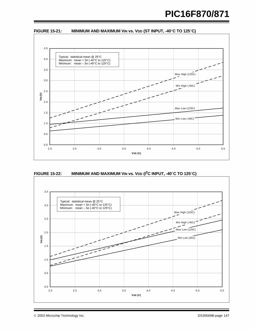
PIC16F870/871
FIGURE 15-21: MINIMUM AND MAXIMUM VIN vs. VDD (ST INPUT, -40°C TO 125°C)
FIGURE 15-22: MINIMUM AND MAXIMUM VIN vs. VDD (I2C INPUT, -40°C TO 125°C)
0.0
0.5
1.0
1.5
2.0
2.5
3.0
3.5
4.0
4.5
2.0 2.5 3.0 3.5 4.0 4.5 5.0 5.5
VDD (V)
VIN
(V
)
Max High (125C)
Max Low (125C)
Min High (-40C)
Min Low (-40C)
Typical: statistical mean @ 25°CMaximum: mean + 3σ (-40°C to 125°C) Minimum: mean – 3σ (-40°C to 125°C)
0.0
0.5
1.0
1.5
2.0
2.5
3.0
3.5
2.0 2.5 3.0 3.5 4.0 4.5 5.0 5.5
VDD (V)
VIN
(V
)
Max High (125C)
Max Low (125C)
Min High (-40C)
Min Low (25C)
Typical: statistical mean @ 25°CMaximum: mean + 3σ (-40°C to 125°C) Minimum: mean – 3σ (-40°C to 125°C)
2003 Microchip Technology Inc. DS30569B-page 147
PIC16F870/871
NOTES:
DS30569B-page 148 2003 Microchip Technology Inc.
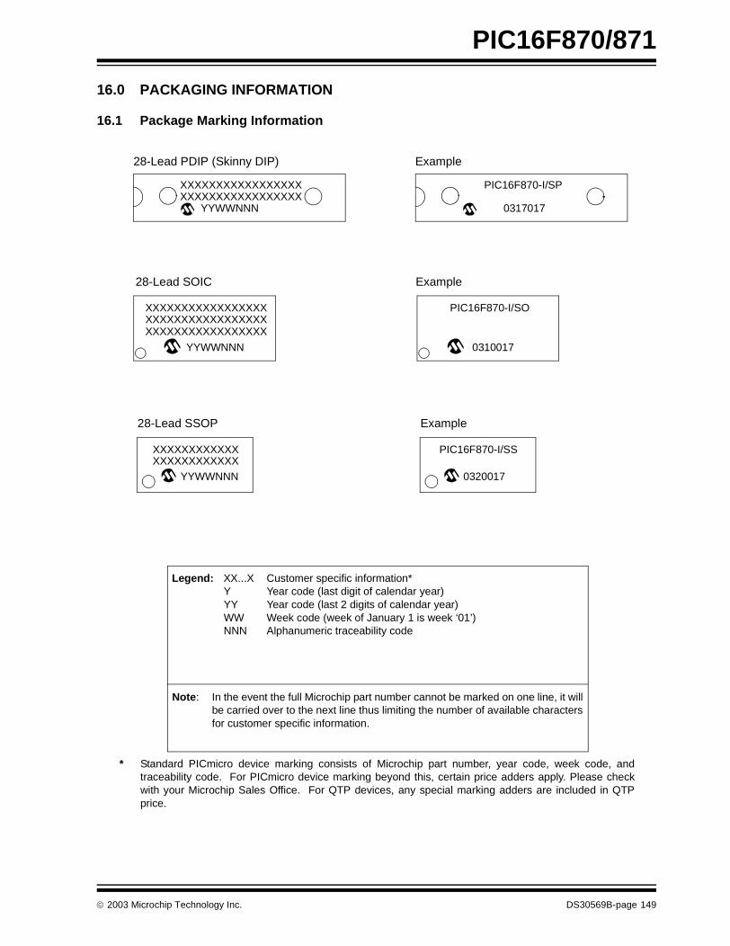
PIC16F870/871
16.0 PACKAGING INFORMATION
16.1 Package Marking Information
XXXXXXXXXXXXXXXXXYYWWNNN
28-Lead PDIP (Skinny DIP) Example
XXXXXXXXXXXXXXXXX
0317017
PIC16F870-I/SP
28-Lead SOIC
YYWWNNN
Example
XXXXXXXXXXXXXXXXXXXXXXXXXXXXXXXXXX
XXXXXXXXXXXXXXXXX
0310017
PIC16F870-I/SO
28-Lead SSOP
YYWWNNNXXXXXXXXXXXXXXXXXXXXXXXX
Example
0320017
PIC16F870-I/SS
Legend: XX...X Customer specific information*Y Year code (last digit of calendar year)YY Year code (last 2 digits of calendar year)WW Week code (week of January 1 is week ‘01’)NNN Alphanumeric traceability code
Note: In the event the full Microchip part number cannot be marked on one line, it willbe carried over to the next line thus limiting the number of available charactersfor customer specific information.
* Standard PICmicro device marking consists of Microchip part number, year code, week code, andtraceability code. For PICmicro device marking beyond this, certain price adders apply. Please checkwith your Microchip Sales Office. For QTP devices, any special marking adders are included in QTPprice.
2003 Microchip Technology Inc. DS30569B-page 149

PIC16F870/871
Package Marking Information (Cont’d)
XXXXXXXXXXXXXXXXXX
YYWWNNN
40-Lead PDIP Example
XXXXXXXXXXXXXXXXXXXXXXXXXXXXXXXXXXXX
PIC16F871-I/P
0312017
44-Lead TQFP Example
XXXXXXXXXXXXXXXXXXXXXXXXXXXXXX
YYWWNNN
PIC16F871-I/PT
0320017
44-Lead PLCC Example
XXXXXXXXXXXXXXXXXXXXXXXXXXXXXXYYWWNNN
PIC16F871-I/L
0320017
DS30569B-page 150 2003 Microchip Technology Inc.
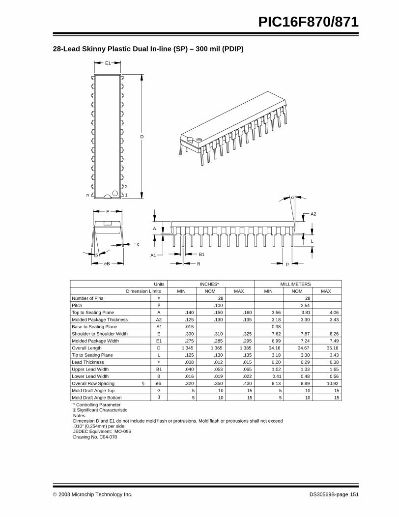
PIC16F870/871
28-Lead Skinny Plastic Dual In-line (SP) – 300 mil (PDIP)
1510515105βMold Draft Angle Bottom
1510515105αMold Draft Angle Top
10.928.898.13.430.350.320eBOverall Row Spacing §
0.560.480.41.022.019.016BLower Lead Width
1.651.331.02.065.053.040B1Upper Lead Width
0.380.290.20.015.012.008cLead Thickness
3.433.303.18.135.130.125LTip to Seating Plane
35.1834.6734.161.3851.3651.345DOverall Length
7.497.246.99.295.285.275E1Molded Package Width
8.267.877.62.325.310.300EShoulder to Shoulder Width
0.38.015A1Base to Seating Plane
3.433.303.18.135.130.125A2Molded Package Thickness
4.063.813.56.160.150.140ATop to Seating Plane
2.54.100pPitch
2828nNumber of Pins
MAXNOMMINMAXNOMMINDimension Limits
MILLIMETERSINCHES*Units
2
1
D
n
E1
c
eB
β
E
α
p
L
A2
B
B1
A
A1
Notes:
JEDEC Equivalent: MO-095Drawing No. C04-070
* Controlling Parameter
Dimension D and E1 do not include mold flash or protrusions. Mold flash or protrusions shall not exceed .010” (0.254mm) per side.
§ Significant Characteristic
2003 Microchip Technology Inc. DS30569B-page 151

PIC16F870/871
28-Lead Plastic Small Outline (SO) – Wide, 300 mil (SOIC)
Foot Angle Top φ 0 4 8 0 4 8
1512015120βMold Draft Angle Bottom1512015120αMold Draft Angle Top
0.510.420.36.020.017.014BLead Width0.330.280.23.013.011.009cLead Thickness
1.270.840.41.050.033.016LFoot Length0.740.500.25.029.020.010hChamfer Distance
18.0817.8717.65.712.704.695DOverall Length7.597.497.32.299.295.288E1Molded Package Width
10.6710.3410.01.420.407.394EOverall Width0.300.200.10.012.008.004A1Standoff §2.392.312.24.094.091.088A2Molded Package Thickness2.642.502.36.104.099.093AOverall Height
1.27.050pPitch2828nNumber of Pins
MAXNOMMINMAXNOMMINDimension LimitsMILLIMETERSINCHES*Units
21
D
p
n
B
E
E1
L
c
β
45°
h
φ
A2
α
A
A1
* Controlling Parameter
Notes:Dimensions D and E1 do not include mold flash or protrusions. Mold flash or protrusions shall not exceed .010” (0.254mm) per side.JEDEC Equivalent: MS-013Drawing No. C04-052
§ Significant Characteristic
DS30569B-page 152 2003 Microchip Technology Inc.
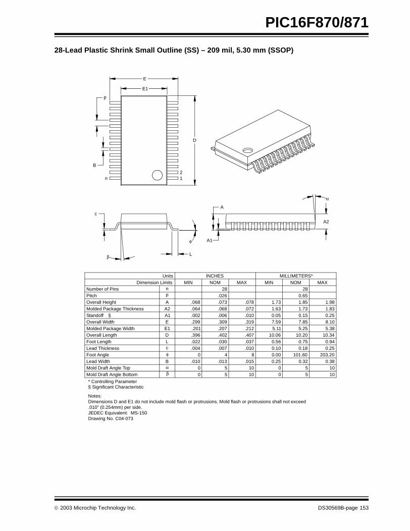
PIC16F870/871
28-Lead Plastic Shrink Small Outline (SS) – 209 mil, 5.30 mm (SSOP)
* Controlling Parameter
Notes:Dimensions D and E1 do not include mold flash or protrusions. Mold flash or protrusions shall not exceed .010” (0.254mm) per side.JEDEC Equivalent: MS-150Drawing No. C04-073
10501050Mold Draft Angle Bottom10501050αMold Draft Angle Top
0.380.320.25.015.013.010BLead Width203.20101.600.00840φFoot Angle
0.250.180.10.010.007.004cLead Thickness0.940.750.56.037.030.022LFoot Length
10.3410.2010.06.407.402.396DOverall Length5.385.255.11.212.207.201E1Molded Package Width8.107.857.59.319.309.299EOverall Width0.250.150.05.010.006.002A1Standoff §1.831.731.63.072.068.064A2Molded Package Thickness1.981.851.73.078.073.068AOverall Height
0.65.026pPitch2828nNumber of Pins
MAXNOMMINMAXNOMMINDimension LimitsMILLIMETERS*INCHESUnits
21
D
p
n
B
E1
E
Lβ
c
φ
α
A2
A1
A
β
§ Significant Characteristic
2003 Microchip Technology Inc. DS30569B-page 153
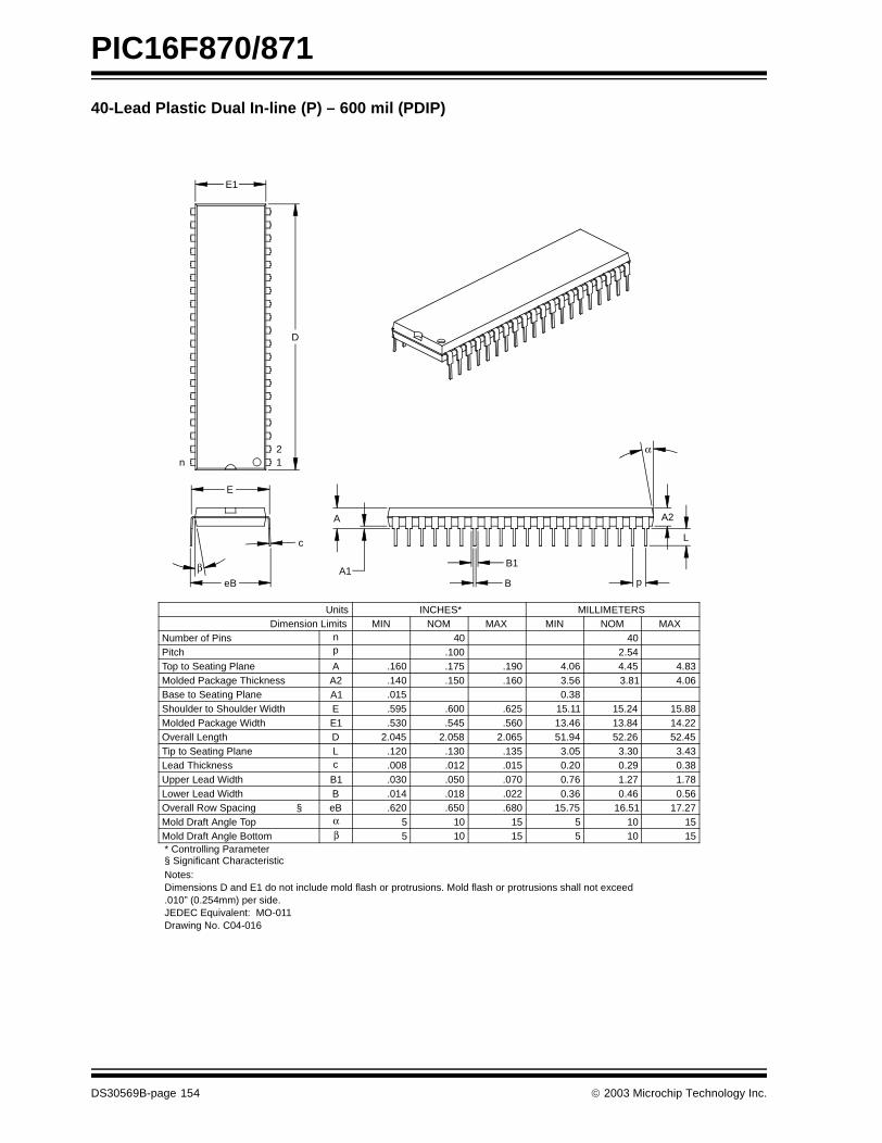
PIC16F870/871
40-Lead Plastic Dual In-line (P) – 600 mil (PDIP)
1510515105βMold Draft Angle Bottom1510515105αMold Draft Angle Top
17.2716.5115.75.680.650.620eBOverall Row Spacing §0.560.460.36.022.018.014BLower Lead Width1.781.270.76.070.050.030B1Upper Lead Width0.380.290.20.015.012.008cLead Thickness3.433.303.05.135.130.120LTip to Seating Plane
52.4552.2651.942.0652.0582.045DOverall Length14.2213.8413.46.560.545.530E1Molded Package Width15.8815.2415.11.625.600.595EShoulder to Shoulder Width
0.38.015A1Base to Seating Plane4.063.813.56.160.150.140A2Molded Package Thickness4.834.454.06.190.175.160ATop to Seating Plane
2.54.100pPitch4040nNumber of Pins
MAXNOMMINMAXNOMMINDimension LimitsMILLIMETERSINCHES*Units
A2
12
D
n
E1
c
βeB
E
α
p
L
B
B1
A
A1
* Controlling Parameter
Notes:Dimensions D and E1 do not include mold flash or protrusions. Mold flash or protrusions shall not exceed .010” (0.254mm) per side.JEDEC Equivalent: MO-011Drawing No. C04-016
§ Significant Characteristic
DS30569B-page 154 2003 Microchip Technology Inc.
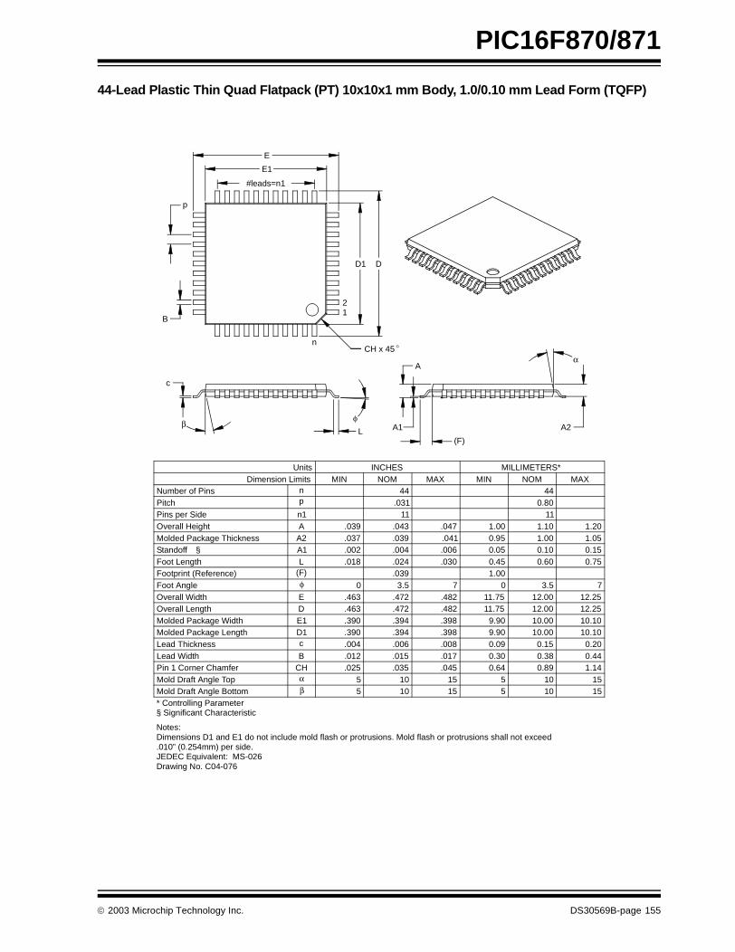
PIC16F870/871
44-Lead Plastic Thin Quad Flatpack (PT) 10x10x1 mm Body, 1.0/0.10 mm Lead Form (TQFP)
* Controlling Parameter
Notes:Dimensions D1 and E1 do not include mold flash or protrusions. Mold flash or protrusions shall not exceed .010” (0.254mm) per side.JEDEC Equivalent: MS-026Drawing No. C04-076
1.140.890.64.045.035.025CHPin 1 Corner Chamfer
1.00.039(F)Footprint (Reference)
(F)
A
A1 A2
α
E
E1
#leads=n1
p
B
D1 D
n
12
φ
c
βL
Units INCHES MILLIMETERS*Dimension Limits MIN NOM MAX MIN NOM MAX
Number of Pins n 44 44Pitch p .031 0.80
Overall Height A .039 .043 .047 1.00 1.10 1.20Molded Package Thickness A2 .037 .039 .041 0.95 1.00 1.05Standoff § A1 .002 .004 .006 0.05 0.10 0.15Foot Length L .018 .024 .030 0.45 0.60 0.75
Foot Angle φ 0 3.5 7 0 3.5 7Overall Width E .463 .472 .482 11.75 12.00 12.25Overall Length D .463 .472 .482 11.75 12.00 12.25Molded Package Width E1 .390 .394 .398 9.90 10.00 10.10Molded Package Length D1 .390 .394 .398 9.90 10.00 10.10
Pins per Side n1 11 11
Lead Thickness c .004 .006 .008 0.09 0.15 0.20Lead Width B .012 .015 .017 0.30 0.38 0.44
Mold Draft Angle Top α 5 10 15 5 10 15Mold Draft Angle Bottom β 5 10 15 5 10 15
CH x 45 °
§ Significant Characteristic
2003 Microchip Technology Inc. DS30569B-page 155
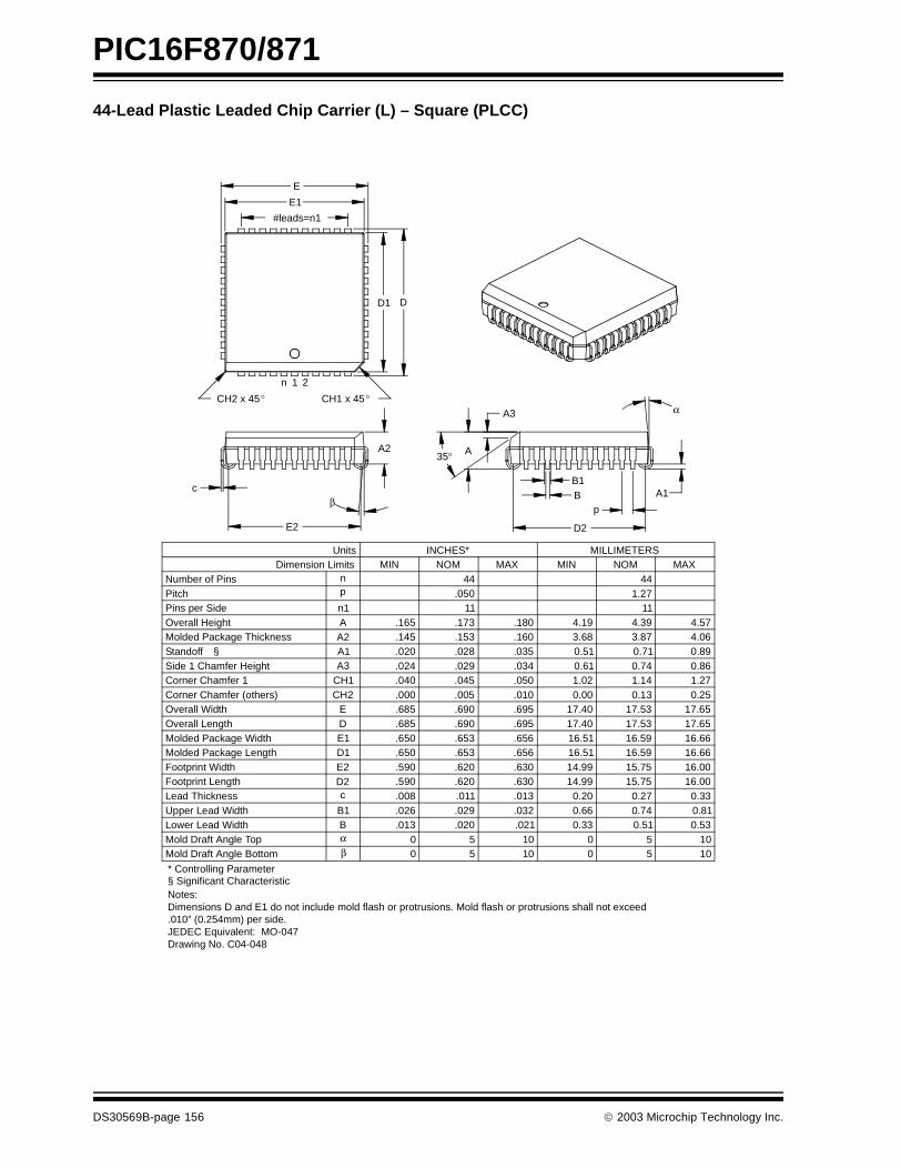
PIC16F870/871
44-Lead Plastic Leaded Chip Carrier (L) – Square (PLCC)
CH2 x 45° CH1 x 45°
10501050βMold Draft Angle Bottom10501050αMold Draft Angle Top
0.530.510.33.021.020.013B0.810.740.66.032.029.026B1Upper Lead Width0.330.270.20.013.011.008cLead Thickness
1111n1Pins per Side
16.0015.7514.99.630.620.590D2Footprint Length16.0015.7514.99.630.620.590E2Footprint Width16.6616.5916.51.656.653.650D1Molded Package Length16.6616.5916.51.656.653.650E1Molded Package Width17.6517.5317.40.695.690.685DOverall Length17.6517.5317.40.695.690.685EOverall Width
0.250.130.00.010.005.000CH2Corner Chamfer (others)1.271.141.02.050.045.040CH1Corner Chamfer 10.860.740.61.034.029.024A3Side 1 Chamfer Height
0.51.020A1Standoff §A2Molded Package Thickness
4.574.394.19.180.173.165AOverall Height
1.27.050pPitch4444nNumber of Pins
MAXNOMMINMAXNOMMINDimension LimitsMILLIMETERSINCHES*Units
β
A2
c
E2
2
DD1
n
#leads=n1
E
E1
1
α
p
A3
A35°
B1B
D2
A1
.145 .153 .160 3.68 3.87 4.06.028 .035 0.71 0.89
Lower Lead Width
* Controlling Parameter
Notes:Dimensions D and E1 do not include mold flash or protrusions. Mold flash or protrusions shall not exceed .010” (0.254mm) per side.JEDEC Equivalent: MO-047Drawing No. C04-048
§ Significant Characteristic
DS30569B-page 156 2003 Microchip Technology Inc.

PIC16F870/871
APPENDIX A: REVISION HISTORY
Revision A (December 1999)
Original data sheet for the PIC16F870/871 family.
Revision B (April 2003)
This revision includes the DC and AC CharacteristicsGraphs and Tables. The Electrical Specifications inSection 14.0 have been updated and there have beenminor corrections to the data sheet text.
APPENDIX B: DEVICE DIFFERENCES
The differences between the devices listed in this datasheet are shown in Table B-1.
TABLE B-1: DEVICE DIFFERENCES
Feature PIC16F870 PIC16F871
On-chip Program Memory (Kbytes) 2K 2K
Data Memory (bytes) 128 128
Boot Block (bytes) 2048 512
Timer1 Low Power Option Yes No
I/O Ports Ports A, B, C Ports A, B, C, D, E
A/D Channels 5 8
External Memory Interface No No
Package Types 28-pin DIP, SOIC, SSOP 40-pin PDIP, 44-pin PLCC, TQFP
2003 Microchip Technology Inc. DS30569B-page 157
PIC16F870/871
APPENDIX C: CONVERSION CONSIDERATIONS
This appendix discusses the considerations for con-verting from previous versions of a device to the oneslisted in this data sheet. Typically, these changes aredue to the differences in the process technology used.An example of this type of conversion is from aPIC17C756 to a PIC18F8720.
Not Applicable
APPENDIX D: MIGRATION FROM MID-RANGE TO ENHANCED DEVICES
A detailed discussion of the differences between themid-range MCU devices (i.e., PIC16CXXX) and theenhanced devices (i.e., PIC18FXXX) is provided inAN716, “Migrating Designs from PIC16C74A/74B toPIC18C442.” The changes discussed, while devicespecific, are generally applicable to all mid-range toenhanced device migrations.
This Application Note is available as Literature NumberDS00716.
DS30569B-page 158 2003 Microchip Technology Inc.
PIC16F870/871
APPENDIX E: MIGRATION FROM HIGH-END TO ENHANCED DEVICES
A detailed discussion of the migration pathway and dif-ferences between the high-end MCU devices (i.e.,PIC17CXXX) and the enhanced devices (i.e.,PIC18FXXXX) is provided in AN726, “PIC17CXXX toPIC18CXXX Migration.” This Application Note isavailable as Literature Number DS00726.
2003 Microchip Technology Inc. DS30569B-page 159

PIC16F870/871
NOTES:
DS30569B-page 160 2003 Microchip Technology Inc.
PIC16F870/871
INDEX
AA/D ...................................................................................... 79
Acquisition Requirements ........................................... 82ADCON0 Register....................................................... 79ADCON1 Register....................................................... 79ADIF Bit....................................................................... 80ADRESH Register....................................................... 79ADRESL Register ....................................................... 79Analog Port Pins ................................................... 41, 42Associated Registers and Bits .................................... 85Calculating Acquisition Time....................................... 82Configuring Analog Port Pins...................................... 83Configuring the Interrupt ............................................. 81Configuring the Module............................................... 81Conversion Clock........................................................ 83Conversions ................................................................ 84Delays ......................................................................... 82Effects of a RESET ..................................................... 85GO/DONE Bit.............................................................. 80Internal Sampling Switch (Rss) Impedance ................ 82Operation During SLEEP............................................ 85Result Registers.......................................................... 84Source Impedance...................................................... 82Time Delays ................................................................ 82
Absolute Maximum Ratings .............................................. 117ADCON0 Register............................................................... 13ADCON1 Register............................................................... 14ADRESH Registers ............................................................. 13ADRESL Register ............................................................... 14Analog-to-Digital Converter. See A/D.Application Notes
AN552 (Implementing Wake-up on Key Stroke) ......... 35AN556 (Implementing a Table Read) ......................... 24
AssemblerMPASM Assembler................................................... 111
Asynchronous ReceptionAssociated Registers .................................................. 69
Asynchronous Reception (9-bit Mode)Associated Registers .................................................. 71
BBanking, Data Memory ....................................................... 11Baud Rate Generator (BRG)
Associated Registers .................................................. 63Block Diagrams
A/D .............................................................................. 81Analog Input Model ..................................................... 82Capture Mode Operation ............................................ 56Compare Mode Operation .......................................... 57Interrupt Logic ............................................................. 97On-Chip RESET Circuit .............................................. 91PIC16F870.................................................................... 5PIC16F871.................................................................... 6PORTC (Peripheral Output Override) ......................... 37PORTD (In I/O Port Mode).......................................... 38PORTD and PORTE (Parallel Slave Port) .................. 42PORTE (In I/O Port Mode).......................................... 39PWM Mode ................................................................. 58RA3:RA0 and RA5 Pins .............................................. 33RA4/T0CKI Pin............................................................ 33RB3:RB0 Pins ............................................................. 35RB7:RB4 Pins ............................................................. 35Timer0/WDT Prescaler ............................................... 45
Timer1 ........................................................................ 50Timer2 ........................................................................ 53USART Asynchronous Receive.................................. 68USART Asynchronous Receive (9-bit Mode) ............. 70USART Transmit ........................................................ 66Watchdog Timer ......................................................... 99
BOR. See Brown-out Reset.BRGH Bit ............................................................................ 63Brown-out Reset (BOR).................................... 87, 91, 92, 93
BOR Status (BOR Bit) ................................................ 23
CC Compilers
MPLAB C17.............................................................. 112MPLAB C18.............................................................. 112MPLAB C30.............................................................. 112
Capture/Compare/PWM (CCP) .......................................... 55Associated Registers
Capture, Compare and Timer1........................... 59PWM and Timer2................................................ 60
Capture Mode............................................................. 56CCP1IF............................................................... 56Prescaler ............................................................ 56
CCP Timer Resources................................................ 55Compare
Special Trigger Output of CCP1......................... 57Compare Mode........................................................... 57
Software Interrupt Mode..................................... 57Special Event Trigger ......................................... 57
PWM Mode................................................................. 58Duty Cycle .......................................................... 58Example Frequencies/Resolutions (table).......... 59PWM Period ....................................................... 58Setup for PWM Operation .................................. 59
Special Event Trigger and A/D Conversions .............. 57CCP. See Capture/Compare/PWM.CCP1CON Register............................................................ 13CCP1M0 Bit ........................................................................ 55CCP1M1 Bit ........................................................................ 55CCP1M2 Bit ........................................................................ 55CCP1M3 Bit ........................................................................ 55CCP1X Bit .......................................................................... 55CCP1Y Bit .......................................................................... 55CCPR1H Register......................................................... 13, 55CCPR1L Register ......................................................... 13, 55Code Examples
Changing Between Capture Prescalers ..................... 56EEPROM Data Read.................................................. 29EEPROM Data Write .................................................. 29FLASH Program Read................................................ 30FLASH Program Write................................................ 31Indirect Addressing..................................................... 24Initializing PORTA ...................................................... 33Saving STATUS, W and PCLATH Registers
in RAM................................................................ 98Code Protected Operation
Data EEPROM and FLASH Program Memory ........... 31Code Protection.......................................................... 87, 101Computed GOTO................................................................ 24Configuration Bits ............................................................... 87Configuration Word............................................................. 88Conversion Considerations............................................... 158
2003 Microchip Technology Inc. DS30569B-page 161
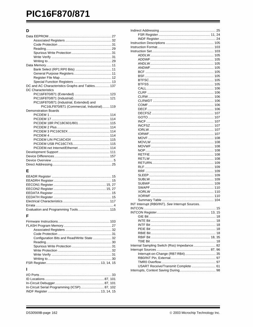
PIC16F870/871
DData EEPROM .................................................................... 27
Associated Registers .................................................. 32Code Protection .......................................................... 31Reading....................................................................... 29Spurious Write Protection ........................................... 31Write Verify ................................................................. 31Writing to ..................................................................... 29
Data Memory....................................................................... 11Bank Select (RP1:RP0 Bits) ....................................... 11General Purpose Registers......................................... 11Register File Map........................................................ 12Special Function Registers ......................................... 13
DC and AC Characteristics Graphs and Tables................ 137DC Characteristics
PIC16F870/871 (Extended) ...................................... 123PIC16F870/871 (Industrial) ....................................... 121PIC16F870/871 (Industrial, Extended) and
PIC16LF870/871 (Commercial, Industrial)........ 119Demonstration Boards
PICDEM 1 ................................................................. 114PICDEM 17 ............................................................... 114PICDEM 18R PIC18C601/801.................................. 115PICDEM 2 Plus ......................................................... 114PICDEM 3 PIC16C92X ............................................. 114PICDEM 4 ................................................................. 114PICDEM LIN PIC16C43X ......................................... 115PICDEM USB PIC16C7X5........................................ 115PICDEM.net Internet/Ethernet .................................. 114
Development Support ....................................................... 111Device Differences ............................................................ 157Device Overview ................................................................... 5Direct Addressing................................................................ 25
EEEADR Register ................................................................. 15EEADRH Register............................................................... 15EECON1 Register ......................................................... 15, 27EECON2 Register ......................................................... 15, 27EEDATA Register ............................................................... 15EEDATH Register ............................................................... 15Electrical Characteristics................................................... 117Errata .................................................................................... 4Evaluation and Programming Tools .................................. 115
FFirmware Instructions........................................................ 103FLASH Program Memory.................................................... 27
Associated Registers .................................................. 32Code Protection .......................................................... 31Configuration Bits and Read/Write State .................... 32Reading....................................................................... 30Spurious Write Protection ........................................... 31Write Protection .......................................................... 32Write Verify ................................................................. 31Writing to ..................................................................... 30
FSR Register........................................................... 13, 14, 15
II/O Ports .............................................................................. 33ID Locations ................................................................ 87, 101In-Circuit Debugger ..................................................... 87, 101In-Circuit Serial Programming (ICSP) ......................... 87, 102INDF Register ......................................................... 13, 14, 15
Indirect Addressing ............................................................. 25FSR Register ........................................................ 11, 24INDF Register ............................................................. 24
Instruction Descriptions .................................................... 105Instruction Format............................................................. 103Instruction Set................................................................... 103
ADDLW..................................................................... 105ADDWF..................................................................... 105ANDLW..................................................................... 105ANDWF..................................................................... 105BCF .......................................................................... 105BSF........................................................................... 105BTFSC...................................................................... 105BTFSS ...................................................................... 105CALL......................................................................... 106CLRF ........................................................................ 106CLRW ....................................................................... 106CLRWDT .................................................................. 106COMF ....................................................................... 106DECF........................................................................ 106DECFSZ ................................................................... 107GOTO ....................................................................... 107INCF ......................................................................... 107INCFSZ..................................................................... 107IORLW...................................................................... 107IORWF...................................................................... 107MOVF ....................................................................... 108MOVLW .................................................................... 108MOVWF.................................................................... 108NOP.......................................................................... 108RETFIE..................................................................... 108RETLW ..................................................................... 108RETURN................................................................... 109RLF........................................................................... 109RRF .......................................................................... 109SLEEP ...................................................................... 109SUBLW..................................................................... 109SUBWF..................................................................... 109SWAPF..................................................................... 110XORLW .................................................................... 110XORWF .................................................................... 110Summary Table ........................................................ 104
INT Interrupt (RB0/INT). See Interrupt Sources.INTCON .............................................................................. 15INTCON Register.......................................................... 13, 15
GIE Bit ........................................................................ 18INTE Bit ...................................................................... 18INTF Bit ...................................................................... 18PEIE Bit ...................................................................... 18RBIE Bit ...................................................................... 18RBIF Bit ................................................................ 18, 35T0IE Bit ....................................................................... 18
Internal Sampling Switch (Rss) Impedance........................ 82Interrupt Sources .......................................................... 87, 96
Interrupt-on-Change (RB7:RB4) ................................. 35RB0/INT Pin, External................................................. 97TMR0 Overflow........................................................... 97USART Receive/Transmit Complete .......................... 61
Interrupts, Context Saving During....................................... 98
DS30569B-page 162 2003 Microchip Technology Inc.
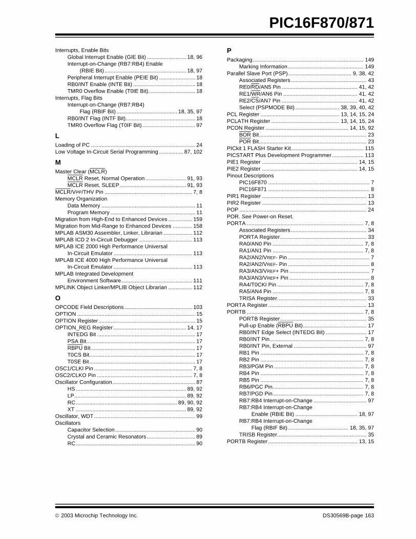
PIC16F870/871
Interrupts, Enable BitsGlobal Interrupt Enable (GIE Bit) .......................... 18, 96Interrupt-on-Change (RB7:RB4) Enable
(RBIE Bit) ...................................................... 18, 97Peripheral Interrupt Enable (PEIE Bit) ........................ 18RB0/INT Enable (INTE Bit) ......................................... 18TMR0 Overflow Enable (T0IE Bit)............................... 18
Interrupts, Flag BitsInterrupt-on-Change (RB7:RB4)
Flag (RBIF Bit) ........................................ 18, 35, 97RB0/INT Flag (INTF Bit).............................................. 18TMR0 Overflow Flag (T0IF Bit) ................................... 97
LLoading of PC ..................................................................... 24Low Voltage In-Circuit Serial Programming ................ 87, 102
MMaster Clear (MCLR)
MCLR Reset, Normal Operation ........................... 91, 93MCLR Reset, SLEEP............................................ 91, 93
MCLR/VPP/THV Pin .......................................................... 7, 8Memory Organization
Data Memory .............................................................. 11Program Memory ........................................................ 11
Migration from High-End to Enhanced Devices ................ 159Migration from Mid-Range to Enhanced Devices ............. 158MPLAB ASM30 Assembler, Linker, Librarian ................... 112MPLAB ICD 2 In-Circuit Debugger ................................... 113MPLAB ICE 2000 High Performance Universal
In-Circuit Emulator .................................................... 113MPLAB ICE 4000 High Performance Universal
In-Circuit Emulator .................................................... 113MPLAB Integrated Development
Environment Software............................................... 111MPLINK Object Linker/MPLIB Object Librarian ................ 112
OOPCODE Field Descriptions ............................................. 103OPTION .............................................................................. 15OPTION Register ................................................................ 15OPTION_REG Register ................................................ 14, 17
INTEDG Bit ................................................................. 17PSA Bit........................................................................ 17RBPU Bit..................................................................... 17T0CS Bit...................................................................... 17T0SE Bit...................................................................... 17
OSC1/CLKI Pin ................................................................. 7, 8OSC2/CLKO Pin ............................................................... 7, 8Oscillator Configuration....................................................... 87
HS......................................................................... 89, 92LP.......................................................................... 89, 92RC................................................................... 89, 90, 92XT ......................................................................... 89, 92
Oscillator, WDT................................................................... 99Oscillators
Capacitor Selection..................................................... 90Crystal and Ceramic Resonators ................................ 89RC............................................................................... 90
PPackaging......................................................................... 149
Marking Information.................................................. 149Parallel Slave Port (PSP).......................................... 9, 38, 42
Associated Registers.................................................. 43RE0/RD/AN5 Pin .................................................. 41, 42RE1/WR/AN6 Pin ................................................. 41, 42RE2/CS/AN7 Pin .................................................. 41, 42Select (PSPMODE Bit) ............................. 38, 39, 40, 42
PCL Register .................................................... 13, 14, 15, 24PCLATH Register ............................................. 13, 14, 15, 24PCON Register ....................................................... 14, 15, 92
BOR Bit....................................................................... 23POR Bit....................................................................... 23
PICkit 1 FLASH Starter Kit................................................ 115PICSTART Plus Development Programmer..................... 113PIE1 Register ............................................................... 14, 15PIE2 Register ............................................................... 14, 15Pinout Descriptions
PIC16F870 ................................................................... 7PIC16F871 ................................................................... 8
PIR1 Register ..................................................................... 13PIR2 Register ..................................................................... 13POP .................................................................................... 24POR. See Power-on Reset.PORTA ............................................................................. 7, 8
Associated Registers.................................................. 34PORTA Register......................................................... 33RA0/AN0 Pin ............................................................ 7, 8RA1/AN1 Pin ............................................................ 7, 8RA2/AN2/VREF- Pin ...................................................... 7RA2/AN2/VREF- Pin ...................................................... 8RA3/AN3/VREF+ Pin ..................................................... 7RA3/AN3/VREF+ Pin ..................................................... 8RA4/T0CKI Pin ......................................................... 7, 8RA5/AN4 Pin ............................................................ 7, 8TRISA Register........................................................... 33
PORTA Register ................................................................. 13PORTB ............................................................................. 7, 8
PORTB Register......................................................... 35Pull-up Enable (RBPU Bit).......................................... 17RB0/INT Edge Select (INTEDG Bit) ........................... 17RB0/INT Pin.............................................................. 7, 8RB0/INT Pin, External ................................................ 97RB1 Pin .................................................................... 7, 8RB2 Pin .................................................................... 7, 8RB3/PGM Pin ........................................................... 7, 8RB4 Pin .................................................................... 7, 8RB5 Pin .................................................................... 7, 8RB6/PGC Pin............................................................ 7, 8RB7/PGD Pin............................................................ 7, 8RB7:RB4 Interrupt-on-Change ................................... 97RB7:RB4 Interrupt-on-Change
Enable (RBIE Bit) ......................................... 18, 97RB7:RB4 Interrupt-on-Change
Flag (RBIF Bit)........................................ 18, 35, 97TRISB Register........................................................... 35
PORTB Register ........................................................... 13, 15
2003 Microchip Technology Inc. DS30569B-page 163
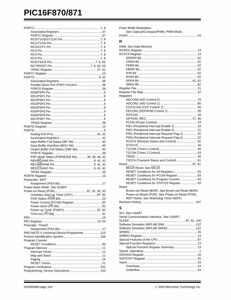
PIC16F870/871
PORTC.............................................................................. 7, 8Associated Registers .................................................. 37PORTC Register ......................................................... 37RC0/T1OSO/T1CKI Pin ............................................ 7, 8RC1/T1OSI Pin ......................................................... 7, 8RC2/CCP1 Pin .......................................................... 7, 8RC3 Pin..................................................................... 7, 8RC4 Pin..................................................................... 7, 8RC5 Pin..................................................................... 7, 8RC6/TX/CK Pin ................................................... 7, 8, 62RC7/RX/DT Pin............................................. 7, 8, 62, 63TRISC Register ..................................................... 37, 61
PORTC Register ................................................................. 13PORTD............................................................................ 9, 42
Associated Registers .................................................. 38Parallel Slave Port (PSP) Function ............................. 38PORTD Register ......................................................... 38RD0/PSP0 Pin .............................................................. 9RD1/PSP1 Pin .............................................................. 9RD2/PSP2 Pin .............................................................. 9RD3/PSP3 Pin .............................................................. 9RD4/PSP4 Pin .............................................................. 9RD5/PSP5 Pin .............................................................. 9RD6/PSP6 Pin .............................................................. 9RD7/PSP7 Pin .............................................................. 9TRISD Register ........................................................... 38
PORTD Register ................................................................. 13PORTE.................................................................................. 9
Analog Port Pins ................................................... 41, 42Associated Registers .................................................. 41Input Buffer Full Status (IBF Bit) ................................. 40Input Buffer Overflow (IBOV Bit) ................................. 40Output Buffer Full Status (OBF Bit)............................. 40PORTE Register ......................................................... 39PSP Mode Select (PSPMODE Bit) ........... 38, 39, 40, 42RE0/RD/AN5 Pin............................................... 9, 41, 42RE1/WR/AN6 Pin.............................................. 9, 41, 42RE2/CS/AN7 Pin............................................... 9, 41, 42TRISE Register ........................................................... 39
PORTE Register ................................................................. 13Postscaler, WDT
Assignment (PSA Bit) ................................................. 17Power-down Mode. See SLEEP.Power-on Reset (POR) ..................................... 87, 91, 92, 93
Oscillator Start-up Timer (OST) ............................ 87, 92POR Status (POR Bit)................................................. 23Power Control (PCON) Register ................................. 92Power-down (PD Bit) .................................................. 91Power-up Timer (PWRT) ...................................... 87, 92Time-out (TO Bit) ........................................................ 91
PR2 ..................................................................................... 15PR2 Register................................................................. 14, 53Prescaler, Timer0
Assignment (PSA Bit) ................................................. 17PRO MATE II Universal Device Programmer ................... 113Product Identification System............................................ 169Program Counter
RESET Conditions ...................................................... 93Program Memory ................................................................ 11
Interrupt Vector ........................................................... 11Map and Stack ............................................................ 11Paging......................................................................... 24RESET Vector............................................................. 11
Program Verification.......................................................... 101Programming, Device Instructions .................................... 103
Pulse Width Modulation. See Capture/Compare/PWM, PWM Mode.
PUSH.................................................................................. 24
RRAM. See Data Memory.RCREG Register ................................................................ 13RCSTA Register ................................................................. 13
ADDEN Bit .................................................................. 62CREN Bit .................................................................... 62FERR Bit..................................................................... 62OERR Bit .................................................................... 62RX9 Bit ....................................................................... 62RX9D Bit ..................................................................... 62SPEN Bit............................................................... 61, 62SREN Bit .................................................................... 62
Register File........................................................................ 11Register File Map................................................................ 12Registers
ADCON0 (A/D Control 0)............................................ 79ADCON1 (A/D Control 1)............................................ 80CCP1CON (CCP Control 1)........................................ 55EECON1 (EEPROM Control 1) .................................. 28INTCON...................................................................... 18OPTION_REG ...................................................... 17, 46PCON (Power Control) ............................................... 23PIE1 (Peripheral Interrupt Enable 1)........................... 19PIE2 (Peripheral Interrupt Enable 2)........................... 21PIR1 (Peripheral Interrupt Request Flag 1) ................ 20PIR2 (Peripheral Interrupt Request Flag 2) ................ 22RCSTA (Receive Status and Control) ........................ 62STATUS ..................................................................... 16T1CON (Timer1 Control) ............................................ 49T2CON (Timer 2 Control) ........................................... 53TRISE ......................................................................... 40TXSTA (Transmit Status and Control) ........................ 61
Reset ............................................................................ 87, 91MCLR Reset. See MCLR.RESET Conditions for All Registers ........................... 93RESET Conditions for PCON Register....................... 93RESET Conditions for Program Counter .................... 93RESET Conditions for STATUS Register ................... 93
ResetBrown-out Reset (BOR). See Brown-out Reset (BOR).Power-on Reset (POR). See Power-on Reset (POR).WDT Reset. See Watchdog Timer (WDT).
Revision History................................................................ 157
SSCI. See USARTSerial Communication Interface. See USART.SLEEP .................................................................. 87, 91, 100Software Simulator (MPLAB SIM) .................................... 112Software Simulator (MPLAB SIM30) ................................ 112SPBRG ............................................................................... 15SPBRG Register................................................................. 14Special Features of the CPU .............................................. 87Special Function Registers ................................................. 13
Special Function Register Summary .......................... 13Speed, Operating.................................................................. 1SSPADD Register............................................................... 15SSPSTAT Register ............................................................. 15Stack................................................................................... 24
Overflows.................................................................... 24Underflow ................................................................... 24
DS30569B-page 164 2003 Microchip Technology Inc.
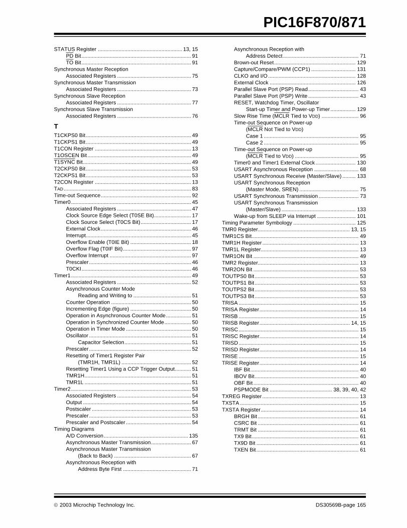
PIC16F870/871
STATUS Register ......................................................... 13, 15PD Bit.......................................................................... 91TO Bit.......................................................................... 91
Synchronous Master ReceptionAssociated Registers .................................................. 75
Synchronous Master TransmissionAssociated Registers .................................................. 73
Synchronous Slave ReceptionAssociated Registers .................................................. 77
Synchronous Slave TransmissionAssociated Registers .................................................. 76
TT1CKPS0 Bit ....................................................................... 49T1CKPS1 Bit ....................................................................... 49T1CON Register ................................................................. 13T1OSCEN Bit ...................................................................... 49T1SYNC Bit......................................................................... 49T2CKPS0 Bit ....................................................................... 53T2CKPS1 Bit ....................................................................... 53T2CON Register ................................................................. 13TAD...................................................................................... 83Time-out Sequence............................................................. 92Timer0................................................................................. 45
Associated Registers .................................................. 47Clock Source Edge Select (T0SE Bit)......................... 17Clock Source Select (T0CS Bit).................................. 17External Clock............................................................. 46Interrupt....................................................................... 45Overflow Enable (T0IE Bit) ......................................... 18Overflow Flag (T0IF Bit).............................................. 97Overflow Interrupt ....................................................... 97Prescaler..................................................................... 46T0CKI.......................................................................... 46
Timer1................................................................................. 49Associated Registers .................................................. 52Asynchronous Counter Mode
Reading and Writing to ....................................... 51Counter Operation ...................................................... 50Incrementing Edge (figure) ......................................... 50Operation in Asynchronous Counter Mode................. 51Operation in Synchronized Counter Mode.................. 50Operation in Timer Mode ............................................ 50Oscillator ..................................................................... 51
Capacitor Selection............................................. 51Prescaler..................................................................... 52Resetting of Timer1 Register Pair
(TMR1H, TMR1L) ............................................... 52Resetting Timer1 Using a CCP Trigger Output........... 51TMR1H........................................................................ 51TMR1L ........................................................................ 51
Timer2................................................................................. 53Associated Registers .................................................. 54Output ......................................................................... 54Postscaler ................................................................... 53Prescaler..................................................................... 53Prescaler and Postscaler ............................................ 54
Timing DiagramsA/D Conversion......................................................... 135Asynchronous Master Transmission........................... 67Asynchronous Master Transmission
(Back to Back) .................................................... 67Asynchronous Reception with
Address Byte First .............................................. 71
Asynchronous Reception with Address Detect ................................................... 71
Brown-out Reset....................................................... 129Capture/Compare/PWM (CCP1) .............................. 131CLKO and I/O ........................................................... 128External Clock .......................................................... 126Parallel Slave Port (PSP) Read.................................. 43Parallel Slave Port (PSP) Write .................................. 43RESET, Watchdog Timer, Oscillator
Start-up Timer and Power-up Timer ................. 129Slow Rise Time (MCLR Tied to VDD) ......................... 96Time-out Sequence on Power-up
(MCLR Not Tied to VDD)Case 1 ................................................................ 95Case 2 ................................................................ 95
Time-out Sequence on Power-up (MCLR Tied to VDD) ........................................... 95
Timer0 and Timer1 External Clock ........................... 130USART Asynchronous Reception .............................. 68USART Synchronous Receive (Master/Slave) ......... 133USART Synchronous Reception
(Master Mode, SREN) ........................................ 75USART Synchronous Transmission ........................... 73USART Synchronous Transmission
(Master/Slave) .................................................. 133Wake-up from SLEEP via Interrupt .......................... 101
Timing Parameter Symbology .......................................... 125TMR0 Register.............................................................. 13, 15TMR1CS Bit........................................................................ 49TMR1H Register ................................................................. 13TMR1L Register.................................................................. 13TMR1ON Bit ....................................................................... 49TMR2 Register.................................................................... 13TMR2ON Bit ....................................................................... 53TOUTPS0 Bit ...................................................................... 53TOUTPS1 Bit ...................................................................... 53TOUTPS2 Bit ...................................................................... 53TOUTPS3 Bit ...................................................................... 53TRISA ................................................................................. 15TRISA Register................................................................... 14TRISB ................................................................................. 15TRISB Register............................................................. 14, 15TRISC................................................................................. 15TRISC Register................................................................... 14TRISD................................................................................. 15TRISD Register................................................................... 14TRISE ................................................................................. 15TRISE Register................................................................... 14
IBF Bit......................................................................... 40IBOV Bit...................................................................... 40OBF Bit ....................................................................... 40PSPMODE Bit .......................................... 38, 39, 40, 42
TXREG Register ................................................................. 13TXSTA ................................................................................ 15TXSTA Register.................................................................. 14
BRGH Bit .................................................................... 61CSRC Bit .................................................................... 61TRMT Bit .................................................................... 61TX9 Bit........................................................................ 61TX9D Bit ..................................................................... 61TXEN Bit ..................................................................... 61
2003 Microchip Technology Inc. DS30569B-page 165
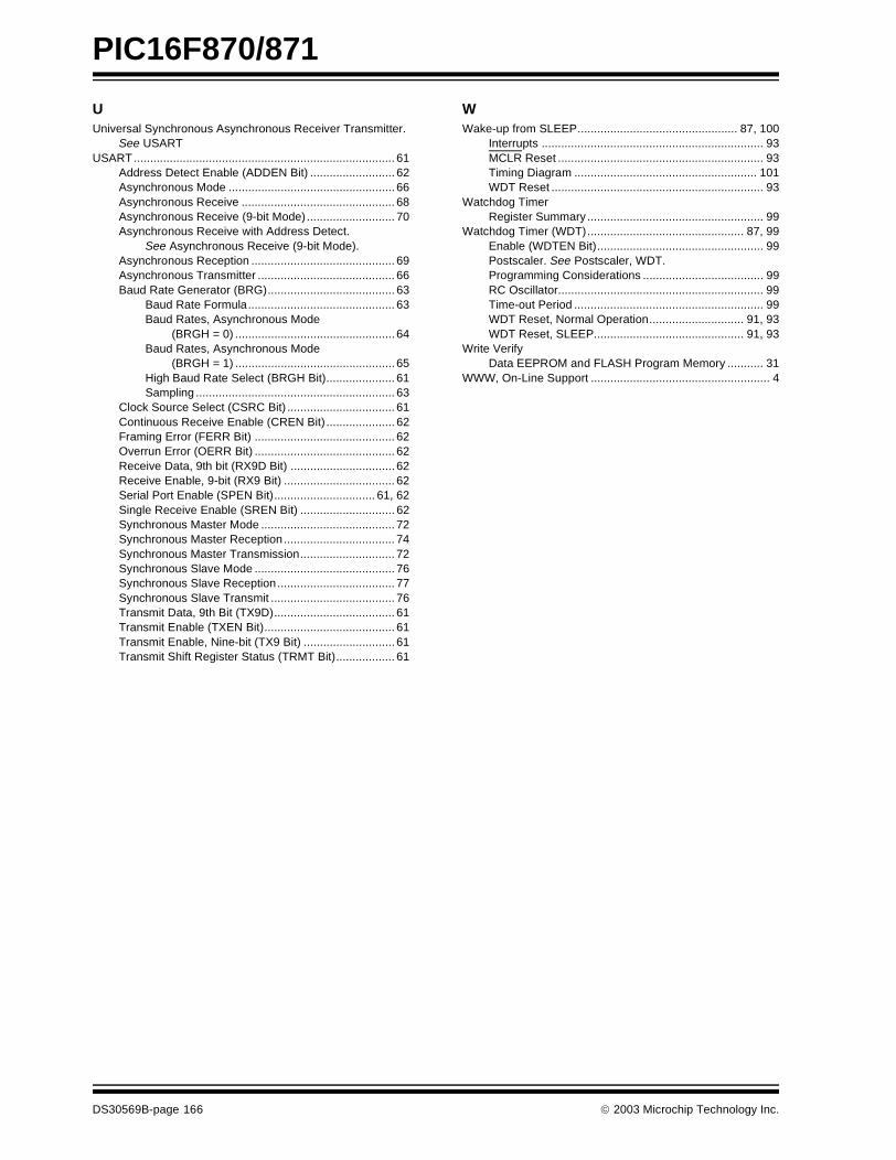
PIC16F870/871
UUniversal Synchronous Asynchronous Receiver Transmitter.
See USARTUSART................................................................................ 61
Address Detect Enable (ADDEN Bit) .......................... 62Asynchronous Mode ................................................... 66Asynchronous Receive ............................................... 68Asynchronous Receive (9-bit Mode)........................... 70Asynchronous Receive with Address Detect.
See Asynchronous Receive (9-bit Mode).Asynchronous Reception ............................................ 69Asynchronous Transmitter .......................................... 66Baud Rate Generator (BRG)....................................... 63
Baud Rate Formula............................................. 63Baud Rates, Asynchronous Mode
(BRGH = 0) ................................................. 64Baud Rates, Asynchronous Mode
(BRGH = 1) ................................................. 65High Baud Rate Select (BRGH Bit)..................... 61Sampling ............................................................. 63
Clock Source Select (CSRC Bit) ................................. 61Continuous Receive Enable (CREN Bit) ..................... 62Framing Error (FERR Bit) ........................................... 62Overrun Error (OERR Bit) ........................................... 62Receive Data, 9th bit (RX9D Bit) ................................ 62Receive Enable, 9-bit (RX9 Bit) .................................. 62Serial Port Enable (SPEN Bit)............................... 61, 62Single Receive Enable (SREN Bit) ............................. 62Synchronous Master Mode ......................................... 72Synchronous Master Reception.................................. 74Synchronous Master Transmission............................. 72Synchronous Slave Mode ........................................... 76Synchronous Slave Reception.................................... 77Synchronous Slave Transmit ...................................... 76Transmit Data, 9th Bit (TX9D)..................................... 61Transmit Enable (TXEN Bit)........................................ 61Transmit Enable, Nine-bit (TX9 Bit) ............................ 61Transmit Shift Register Status (TRMT Bit).................. 61
WWake-up from SLEEP................................................. 87, 100
Interrupts .................................................................... 93MCLR Reset ............................................................... 93Timing Diagram ........................................................ 101WDT Reset ................................................................. 93
Watchdog TimerRegister Summary ...................................................... 99
Watchdog Timer (WDT)................................................ 87, 99Enable (WDTEN Bit)................................................... 99Postscaler. See Postscaler, WDT.Programming Considerations ..................................... 99RC Oscillator............................................................... 99Time-out Period .......................................................... 99WDT Reset, Normal Operation............................. 91, 93WDT Reset, SLEEP.............................................. 91, 93
Write VerifyData EEPROM and FLASH Program Memory ........... 31
WWW, On-Line Support ....................................................... 4
DS30569B-page 166 2003 Microchip Technology Inc.

PIC16F870/871
ON-LINE SUPPORT
Microchip provides on-line support on the MicrochipWorld Wide Web site.
The web site is used by Microchip as a means to makefiles and information easily available to customers. Toview the site, the user must have access to the Internetand a web browser, such as Netscape® or Microsoft®
Internet Explorer. Files are also available for FTPdownload from our FTP site.
Connecting to the Microchip Internet Web Site
The Microchip web site is available at the followingURL:
www.microchip.com
The file transfer site is available by using an FTP ser-vice to connect to:
ftp://ftp.microchip.com
The web site and file transfer site provide a variety ofservices. Users may download files for the latestDevelopment Tools, Data Sheets, Application Notes,User's Guides, Articles and Sample Programs. A vari-ety of Microchip specific business information is alsoavailable, including listings of Microchip sales offices,distributors and factory representatives. Other dataavailable for consideration is:
• Latest Microchip Press Releases• Technical Support Section with Frequently Asked
Questions • Design Tips
• Device Errata• Job Postings• Microchip Consultant Program Member Listing
• Links to other useful web sites related to Microchip Products
• Conferences for products, Development Systems, technical information and more
• Listing of seminars and events
SYSTEMS INFORMATION AND UPGRADE HOT LINE
The Systems Information and Upgrade Line providessystem users a listing of the latest versions of all ofMicrochip's development systems software products.Plus, this line provides information on how customerscan receive the most current upgrade kits.The Hot LineNumbers are:
1-800-755-2345 for U.S. and most of Canada, and
1-480-792-7302 for the rest of the world.
042003
2003 Microchip Technology Inc. DS30569B-page 167

PIC16F870/871
READER RESPONSE
It is our intention to provide you with the best documentation possible to ensure successful use of your Microchip prod-uct. If you wish to provide your comments on organization, clarity, subject matter, and ways in which our documentationcan better serve you, please FAX your comments to the Technical Publications Manager at (480) 792-4150.
Please list the following information, and use this outline to provide us with your comments about this document.
To: Technical Publications Manager
RE: Reader Response
Total Pages Sent ________
From: Name
Company
Address
City / State / ZIP / Country
Telephone: (_______) _________ - _________
Application (optional):
Would you like a reply? Y N
Device: Literature Number:
Questions:
FAX: (______) _________ - _________
DS30569BPIC16F870/871
1. What are the best features of this document?
2. How does this document meet your hardware and software development needs?
3. Do you find the organization of this document easy to follow? If not, why?
4. What additions to the document do you think would enhance the structure and subject?
5. What deletions from the document could be made without affecting the overall usefulness?
6. Is there any incorrect or misleading information (what and where)?
7. How would you improve this document?
DS30569B-page 168 2003 Microchip Technology Inc.
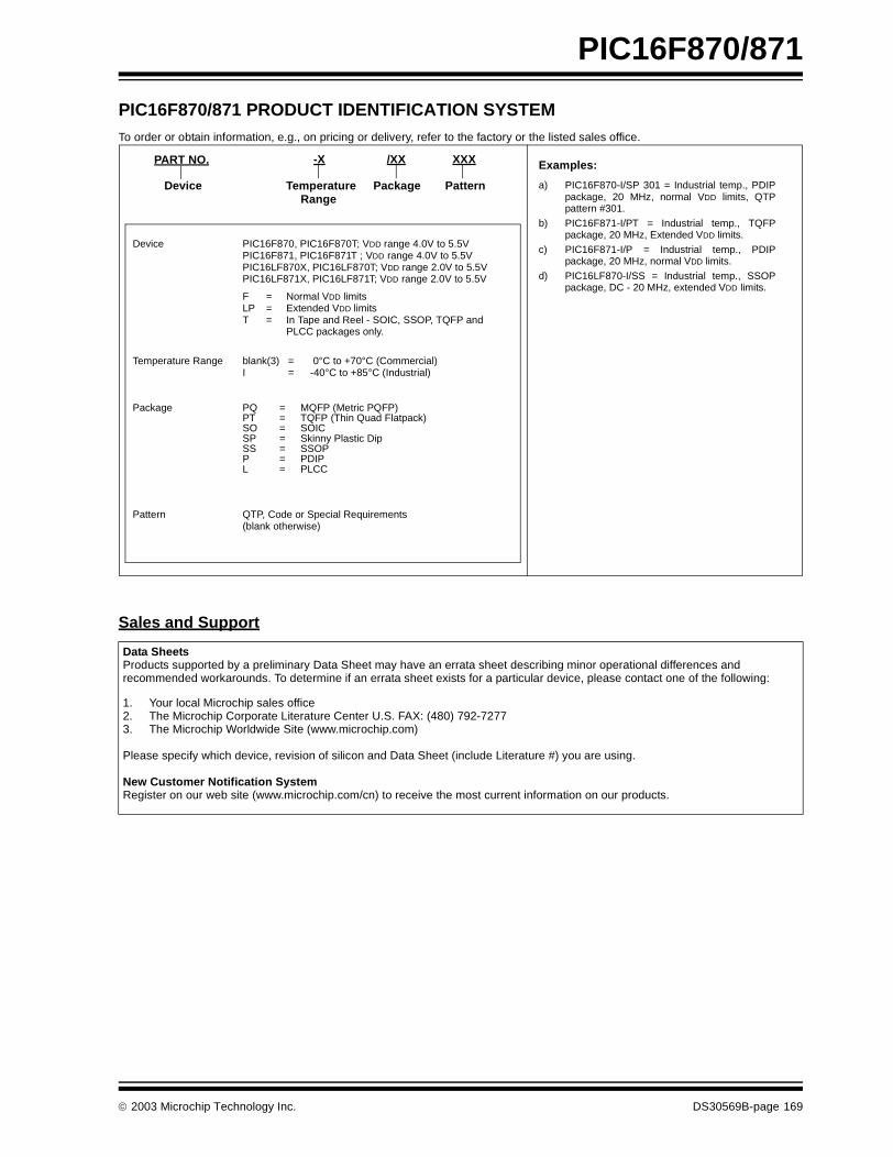
2003 Microchip Technology Inc. DS30569B-page 169
PIC16F870/871
PIC16F870/871 PRODUCT IDENTIFICATION SYSTEMTo order or obtain information, e.g., on pricing or delivery, refer to the factory or the listed sales office.
Sales and Support
Data SheetsProducts supported by a preliminary Data Sheet may have an errata sheet describing minor operational differences and recommended workarounds. To determine if an errata sheet exists for a particular device, please contact one of the following:
1. Your local Microchip sales office2. The Microchip Corporate Literature Center U.S. FAX: (480) 792-72773. The Microchip Worldwide Site (www.microchip.com)
Please specify which device, revision of silicon and Data Sheet (include Literature #) you are using.
New Customer Notification SystemRegister on our web site (www.microchip.com/cn) to receive the most current information on our products.
PART NO. -X /XX XXX
PatternPackageTemperatureRange
Device
Device PIC16F870, PIC16F870T; VDD range 4.0V to 5.5VPIC16F871, PIC16F871T ; VDD range 4.0V to 5.5VPIC16LF870X, PIC16LF870T; VDD range 2.0V to 5.5VPIC16LF871X, PIC16LF871T; VDD range 2.0V to 5.5V
F = Normal VDD limitsLP = Extended VDD limitsT = In Tape and Reel - SOIC, SSOP, TQFP and
PLCC packages only.
Temperature Range blank(3) = 0°C to +70°C (Commercial)I = -40°C to +85°C (Industrial)
Package PQ = MQFP (Metric PQFP)PT = TQFP (Thin Quad Flatpack)SO = SOICSP = Skinny Plastic DipSS = SSOPP = PDIP L = PLCC
Pattern QTP, Code or Special Requirements (blank otherwise)
Examples:
a) PIC16F870-I/SP 301 = Industrial temp., PDIPpackage, 20 MHz, normal VDD limits, QTPpattern #301.
b) PIC16F871-I/PT = Industrial temp., TQFPpackage, 20 MHz, Extended VDD limits.
c) PIC16F871-I/P = Industrial temp., PDIPpackage, 20 MHz, normal VDD limits.
d) PIC16LF870-I/SS = Industrial temp., SSOPpackage, DC - 20 MHz, extended VDD limits.
DS30569B-page 170 2003 Microchip Technology Inc.
AMERICASCorporate Office2355 West Chandler Blvd.Chandler, AZ 85224-6199Tel: 480-792-7200 Fax: 480-792-7277Technical Support: 480-792-7627Web Address: http://www.microchip.com
Atlanta3780 Mansell Road, Suite 130Alpharetta, GA 30022Tel: 770-640-0034 Fax: 770-640-0307
Boston2 Lan Drive, Suite 120Westford, MA 01886Tel: 978-692-3848 Fax: 978-692-3821
Chicago333 Pierce Road, Suite 180Itasca, IL 60143Tel: 630-285-0071 Fax: 630-285-0075
Dallas4570 Westgrove Drive, Suite 160Addison, TX 75001Tel: 972-818-7423 Fax: 972-818-2924
DetroitTri-Atria Office Building 32255 Northwestern Highway, Suite 190Farmington Hills, MI 48334Tel: 248-538-2250 Fax: 248-538-2260
Kokomo2767 S. Albright Road Kokomo, IN 46902Tel: 765-864-8360 Fax: 765-864-8387
Los Angeles18201 Von Karman, Suite 1090Irvine, CA 92612Tel: 949-263-1888 Fax: 949-263-1338
Phoenix2355 West Chandler Blvd.Chandler, AZ 85224-6199Tel: 480-792-7966 Fax: 480-792-4338
San JoseMicrochip Technology Inc.2107 North First Street, Suite 590San Jose, CA 95131Tel: 408-436-7950 Fax: 408-436-7955
Toronto6285 Northam Drive, Suite 108Mississauga, Ontario L4V 1X5, CanadaTel: 905-673-0699 Fax: 905-673-6509
ASIA/PACIFICAustraliaMicrochip Technology Australia Pty LtdMarketing Support DivisionSuite 22, 41 Rawson StreetEpping 2121, NSWAustraliaTel: 61-2-9868-6733 Fax: 61-2-9868-6755China - BeijingMicrochip Technology Consulting (Shanghai)Co., Ltd., Beijing Liaison OfficeUnit 915Bei Hai Wan Tai Bldg.No. 6 Chaoyangmen Beidajie Beijing, 100027, No. ChinaTel: 86-10-85282100 Fax: 86-10-85282104China - ChengduMicrochip Technology Consulting (Shanghai)Co., Ltd., Chengdu Liaison OfficeRm. 2401-2402, 24th Floor, Ming Xing Financial TowerNo. 88 TIDU StreetChengdu 610016, ChinaTel: 86-28-86766200 Fax: 86-28-86766599China - FuzhouMicrochip Technology Consulting (Shanghai)Co., Ltd., Fuzhou Liaison OfficeUnit 28F, World Trade PlazaNo. 71 Wusi RoadFuzhou 350001, ChinaTel: 86-591-7503506 Fax: 86-591-7503521China - Hong Kong SARMicrochip Technology Hongkong Ltd.Unit 901-6, Tower 2, Metroplaza223 Hing Fong RoadKwai Fong, N.T., Hong KongTel: 852-2401-1200 Fax: 852-2401-3431China - ShanghaiMicrochip Technology Consulting (Shanghai)Co., Ltd.Room 701, Bldg. BFar East International PlazaNo. 317 Xian Xia RoadShanghai, 200051Tel: 86-21-6275-5700 Fax: 86-21-6275-5060China - ShenzhenMicrochip Technology Consulting (Shanghai)Co., Ltd., Shenzhen Liaison OfficeRm. 1812, 18/F, Building A, United PlazaNo. 5022 Binhe Road, Futian DistrictShenzhen 518033, ChinaTel: 86-755-82901380 Fax: 86-755-82966626China - QingdaoRm. B505A, Fullhope Plaza,No. 12 Hong Kong Central Rd.Qingdao 266071, ChinaTel: 86-532-5027355 Fax: 86-532-5027205IndiaMicrochip Technology Inc.India Liaison OfficeMarketing Support DivisionDivyasree Chambers1 Floor, Wing A (A3/A4)No. 11, O’Shaugnessey RoadBangalore, 560 025, IndiaTel: 91-80-2290061 Fax: 91-80-2290062
JapanMicrochip Technology Japan K.K.Benex S-1 6F3-18-20, ShinyokohamaKohoku-Ku, Yokohama-shiKanagawa, 222-0033, JapanTel: 81-45-471- 6166 Fax: 81-45-471-6122KoreaMicrochip Technology Korea168-1, Youngbo Bldg. 3 FloorSamsung-Dong, Kangnam-KuSeoul, Korea 135-882Tel: 82-2-554-7200 Fax: 82-2-558-5934SingaporeMicrochip Technology Singapore Pte Ltd.200 Middle Road#07-02 Prime CentreSingapore, 188980Tel: 65-6334-8870 Fax: 65-6334-8850TaiwanMicrochip Technology (Barbados) Inc., Taiwan Branch11F-3, No. 207Tung Hua North RoadTaipei, 105, TaiwanTel: 886-2-2717-7175 Fax: 886-2-2545-0139
EUROPEAustriaMicrochip Technology Austria GmbHDurisolstrasse 2A-4600 WelsAustriaTel: 43-7242-2244-399Fax: 43-7242-2244-393DenmarkMicrochip Technology Nordic ApSRegus Business CentreLautrup hoj 1-3Ballerup DK-2750 DenmarkTel: 45-4420-9895 Fax: 45-4420-9910FranceMicrochip Technology SARLParc d’Activite du Moulin de Massy43 Rue du Saule TrapuBatiment A - ler Etage91300 Massy, FranceTel: 33-1-69-53-63-20 Fax: 33-1-69-30-90-79GermanyMicrochip Technology GmbHSteinheilstrasse 10D-85737 Ismaning, GermanyTel: 49-89-627-144-0 Fax: 49-89-627-144-44ItalyMicrochip Technology SRLVia Quasimodo, 1220025 Legnano (MI)Milan, Italy Tel: 39-0331-742611 Fax: 39-0331-466781United KingdomMicrochip Ltd.505 Eskdale RoadWinnersh TriangleWokingham Berkshire, England RG41 5TUTel: 44-118-921-5869 Fax: 44-118-921-5820
03/25/03
WORLDWIDE SALES AND SERVICE