datasheet.elcodis.comdatasheet.elcodis.com/pdf2/110/73/1107382/cx25870.pdf · data sheet 100381b...
TRANSCRIPT

Data Sheet 100381BSeptember 2001
CX25870/871Video Encoder with Adaptive Flicker Filtering and HDTV Output
Conexant’s CX25870/871 is specifically designed to meet TV out system requirements for the next-generation desktop PCs, notebook PCs, game consoles and set-top boxes. With pin and software-forward compatibility to the Bt868/869, manufacturers can quickly bring to market new solutions that support adaptive flicker filtering, ATSC High-Definition Television (HDTV) output, and resolutions from 320 x 200 (minimum) to 1024 x 768 (maximum).
Adaptive flicker filtering is a Conexant technology in which the encoder looks at the characteristics of the video content on a pixel-by-pixel basis and automatically determines the optimal amount of flicker filtering required. If an end-user wants to work on a spreadsheet while watching a DVD movie in a window, both the text-intensive application requiring a lot of flicker filtering and the DVD movie requiring very little flicker filtering can look their best. The amount of flicker filtering and overscan compensation is entirely flexible.
The CX25870/871 also provides a 3-wire analog RGB or YPRPB HDTV output. While the encoder is in HDTV output mode, the device will automatically insert horizontal tri-level synchronization pulses and vertical synchronization broad pulses. The CX25870/871 is compliant with the EIA770-3, SMPTE 274M/293M/296M standards and supports ATSC HDTV resolutions including 480p, 720p, and 1080i.
All worldwide standard definition outputs are supported, including NTSC-M (N. America, Taiwan), NTSC-J (Japan), PAL-B,D,G,H,I (Europe, Asia), PAL-M (Brazil), PAL-N (Uruguay, Paraguay), PAL-Nc (Argentina), PAL-60 (China) and SECAM. The CX25870 and CX25871 are functionally identical, except the CX25871 can output standard definition video with Macrovision Level 7.1.L1 copy protection capability.
Functional Block Diagram
InputDEMUX
FlickerFilter/Scaler
FIFO24
VideoEncoder
10-Bit
10-Bit
10-Bit
10-Bit
XTALOSC
PLL
DACMUX
DACA
DACB
InternalReference
COMP
FSADJUST
XTL_BFO
VREF
BIASGEN
VBIAS
P[23:0]
XTALIN
XTALOUTCLKOCLKI
SICSID
ALTADDR
HSYNC*VSYNC*BLANK*
FIELD
RESET*SLEEP
SLAVE
PAL
ColorSpace
Conversion#1
ColorSpace
Conversion#2
DACC
DACD
Timing
SerialInterface
ClockGeneration
To InternalClocks
Distinguishing Features• HDTV Output Mode (patents pending)
– Compliant with EIA770-3 and SMPTE274M/293M/296M standards
– Automatic tri-level sync generation– Component (YPRPB) or RGB HDTV
outputs– Direct YPRPB or RGB output from
progressive RGB graphics video in 1080i, 720p, 480p ATSC resolutions
• Software and register forward-compatibility with the Bt868/869
• Ability to accept many different input data formats:– 15/16/24-bit RGB multiplexed or
nonmultiplexed– 16-bit 4:2:2 and 24-bit 4:4:4 YCrCb
multiplexed or nonmultiplexed– Flexible pixel ordering with various
alternate formats• Worldwide video output support:
NTSC-M, J, 4.43, PAL-B, D, G, H, I, M, N, Nc, 60, and SECAM
• Interlaced and noninterlaced outputs• S-Video output (simultaneous with
composite NTSC, PAL, or SECAM)• SCART RGB or Y/C output for Europe
– 4th DAC is composite video– EN50-049 and IEC 933-1 compliant
• 5-Line vertical filtering scaling for overscan compensation and flicker reduction
• Adaptive Flicker Filtering for enhanced image and peaking filters for text sharpness (patents pending)
• CCIR601/ITU-RBT.601 (i.e., 480i) and CCIR656 compatible input modes
• Luma and chroma comb filtering• 4 x 10-bit DACs• Programmable power management• Master, pseudo-master or slave timing
operation• Auto detection of TV• 44 autoconfiguration modes• Wide-Screen Signaling (WSS) support
for variable clock rates– Adheres to EIAJ CPR-1024 and
ITU-R TST.1119-1 standards• Full register set readback capability• 3.3 V operation with scalable low
voltage graphic controller interface from 1.8 V to 1.1 V
• Buffered crystal clock output pin• Component YUV analog output• Colorstream TM (EIA 770.2) and Super
Colorstream TM component video outputs
• Macrovision 7.1.L1 copy protection (CX25871)
• Compact 80-pin PQFP package
Downloaded from Elcodis.com electronic components distributor

100381B Conexant
Downloaded from Elcodis.com electronic components distributor

100381B Conexant
© 2001, Conexant Systems, Inc.All Rights Reserved.
Information in this document is provided in connection with Conexant Systems, Inc. (“Conexant”) products. These materials are provided by Conexant as a service to its customers and may be used for informational purposes only. Conexant assumes no responsibility for errors or omissions in these materials. Conexant may make changes to specifications and product descriptions at any time, without notice. Conexant makes no commitment to update the information and shall have no responsibility whatsoever for conflicts or incompatibilities arising from future changes to its specifications and product descriptions.
No license, express or implied, by estoppel or otherwise, to any intellectual property rights is granted by this document. Except as provided in Conexant’s Terms and Conditions of Sale for such products, Conexant assumes no liability whatsoever.
THESE MATERIALS ARE PROVIDED “AS IS” WITHOUT WARRANTY OF ANY KIND, EITHER EXPRESS OR IMPLIED, RELATING TO SALE AND/OR USE OF CONEXANT PRODUCTS INCLUDING LIABILITY OR WARRANTIES RELATING TO FITNESS FOR A PARTICULAR PURPOSE, CONSEQUENTIAL OR INCIDENTAL DAMAGES, MERCHANTABILITY, OR INFRINGEMENT OF ANY PATENT, COPYRIGHT OR OTHER INTELLECTUAL PROPERTY RIGHT. CONEXANT FURTHER DOES NOT WARRANT THE ACCURACY OR COMPLETENESS OF THE INFORMATION, TEXT, GRAPHICS OR OTHER ITEMS CONTAINED WITHIN THESE MATERIALS. CONEXANT SHALL NOT BE LIABLE FOR ANY SPECIAL, INDIRECT, INCIDENTAL, OR CONSEQUENTIAL DAMAGES, INCLUDING WITHOUT LIMITATION, LOST REVENUES OR LOST PROFITS, WHICH MAY RESULT FROM THE USE OF THESE MATERIALS.
Conexant products are not intended for use in medical, lifesaving or life sustaining applications. Conexant customers using or selling Conexant products for use in such applications do so at their own risk and agree to fully indemnify Conexant for any damages resulting from such improper use or sale.
The following are trademarks of Conexant Systems, Inc.: Conexant™, the Conexant C symbol, and “What’s Next in Communications Technologies”™. Product names or services listed in this publication are for identification purposes only, and may be trademarks of third parties. Third-party brands and names are the property of their respective owners.
For additional disclaimer information, please consult Conexant’s Legal Information posted at www.conexant.com, which is incorporated by reference.
Reader Response: Conexant strives to produce quality documentation and welcomes your feedback. Please send comments and suggestions to [email protected]. For technical questions, contact your local Conexant sales office or field applications engineer.
Ordering Information
Model Number Package Ambient Temperature Range
CX25870 80-pin PQFP 0 °C – 70 °C
CX25871(1) 80-pin PQFP 0 °C – 70 °C
NOTE(S):
1. Macrovision 7.1.L1 compliant (customer must possess Macrovision license to purchase CX25871).
Downloaded from Elcodis.com electronic components distributor

100381B Conexant
Downloaded from Elcodis.com electronic components distributor
100381B Conexant v
Table of Contents
List of Figures. . . . . . . . . . . . . . . . . . . . . . . . . . . . . . . . . . . . . . . . . . . . . . . . . . . . . . . . . . . . . . . . . . vii
List of Tables. . . . . . . . . . . . . . . . . . . . . . . . . . . . . . . . . . . . . . . . . . . . . . . . . . . . . . . . . . . . . . . . . . . . xi
1.0 Functional Description . . . . . . . . . . . . . . . . . . . . . . . . . . . . . . . . . . . . . . . . . . . . . . . . . . . . . . . . . . 1-1
1.1 Pin Descriptions . . . . . . . . . . . . . . . . . . . . . . . . . . . . . . . . . . . . . . . . . . . . . . . . . . . . . . . . . . . . 1-1
1.2 GUI Controller Programmability and Frequency Requirement . . . . . . . . . . . . . . . . . . . . . . . . . . 1-7
1.3 Device Description . . . . . . . . . . . . . . . . . . . . . . . . . . . . . . . . . . . . . . . . . . . . . . . . . . . . . . . . . 1-10
1.3.1 Overview . . . . . . . . . . . . . . . . . . . . . . . . . . . . . . . . . . . . . . . . . . . . . . . . . . . . . . . . . . . 1-10
1.3.2 Serial Interface. . . . . . . . . . . . . . . . . . . . . . . . . . . . . . . . . . . . . . . . . . . . . . . . . . . . . . . 1-10
1.3.3 Low Voltage Graphics Interface . . . . . . . . . . . . . . . . . . . . . . . . . . . . . . . . . . . . . . . . . . 1-11
1.3.4 Reset . . . . . . . . . . . . . . . . . . . . . . . . . . . . . . . . . . . . . . . . . . . . . . . . . . . . . . . . . . . . . . 1-11
1.3.5 Device Initialization . . . . . . . . . . . . . . . . . . . . . . . . . . . . . . . . . . . . . . . . . . . . . . . . . . . 1-12
1.3.6 Clocking and Timing Generation . . . . . . . . . . . . . . . . . . . . . . . . . . . . . . . . . . . . . . . . . . 1-13
1.3.6.1 3:2 Clocking Mode . . . . . . . . . . . . . . . . . . . . . . . . . . . . . . . . . . . . . . . . . . . 1-14
1.3.7 Master, Pseudo-Master, and Slave Interfaces. . . . . . . . . . . . . . . . . . . . . . . . . . . . . . . . . 1-17
1.3.7.1 Master Interface . . . . . . . . . . . . . . . . . . . . . . . . . . . . . . . . . . . . . . . . . . . . . 1-17
1.3.7.2 Reason for BLANK* . . . . . . . . . . . . . . . . . . . . . . . . . . . . . . . . . . . . . . . . . . 1-18
1.3.7.3 Pseudo-Master Interface . . . . . . . . . . . . . . . . . . . . . . . . . . . . . . . . . . . . . . . 1-18
1.3.7.4 Slave Interface . . . . . . . . . . . . . . . . . . . . . . . . . . . . . . . . . . . . . . . . . . . . . . 1-19
1.3.7.5 Slave Interface Without a Crystal . . . . . . . . . . . . . . . . . . . . . . . . . . . . . . . . . 1-20
1.3.8 Autoconfiguration and Interface Bits . . . . . . . . . . . . . . . . . . . . . . . . . . . . . . . . . . . . . . . 1-21
1.3.9 Adaptations for Clock-Limited Master Devices. . . . . . . . . . . . . . . . . . . . . . . . . . . . . . . . 1-25
1.3.10 Input Formats . . . . . . . . . . . . . . . . . . . . . . . . . . . . . . . . . . . . . . . . . . . . . . . . . . . . . . . 1-26
1.3.11 Input Pixel Timing . . . . . . . . . . . . . . . . . . . . . . . . . . . . . . . . . . . . . . . . . . . . . . . . . . . . 1-27
1.3.12 YCrCb Inputs (For Standard TV Outputs). . . . . . . . . . . . . . . . . . . . . . . . . . . . . . . . . . . . 1-27
1.3.13 RGB Inputs (For Standard TV Outputs) . . . . . . . . . . . . . . . . . . . . . . . . . . . . . . . . . . . . . 1-29
1.3.14 Input Pixel Horizontal Sync . . . . . . . . . . . . . . . . . . . . . . . . . . . . . . . . . . . . . . . . . . . . . . 1-29
1.3.15 Input Pixel Vertical Sync . . . . . . . . . . . . . . . . . . . . . . . . . . . . . . . . . . . . . . . . . . . . . . . . 1-30
1.3.16 Input Pixel Blanking . . . . . . . . . . . . . . . . . . . . . . . . . . . . . . . . . . . . . . . . . . . . . . . . . . . 1-30
1.3.17 Overscan Compensation . . . . . . . . . . . . . . . . . . . . . . . . . . . . . . . . . . . . . . . . . . . . . . . . 1-31
1.3.18 Standard Flicker Filtering . . . . . . . . . . . . . . . . . . . . . . . . . . . . . . . . . . . . . . . . . . . . . . . 1-35
1.3.19 Adaptive Flicker Filter . . . . . . . . . . . . . . . . . . . . . . . . . . . . . . . . . . . . . . . . . . . . . . . . . . 1-36
1.3.20 VGA Registers Involved in the TV Out Process . . . . . . . . . . . . . . . . . . . . . . . . . . . . . . . 1-39
1.3.21 Output Modes . . . . . . . . . . . . . . . . . . . . . . . . . . . . . . . . . . . . . . . . . . . . . . . . . . . . . . . 1-40
Downloaded from Elcodis.com electronic components distributor

CX25870/871
Flicker-Free Video Encoder with Ultrascale Technology
vi Conexant 100381B
1.3.22 Analog Horizontal Sync . . . . . . . . . . . . . . . . . . . . . . . . . . . . . . . . . . . . . . . . . . . . . . . . 1-40
1.3.23 Analog Vertical Sync. . . . . . . . . . . . . . . . . . . . . . . . . . . . . . . . . . . . . . . . . . . . . . . . . . . 1-41
1.3.24 Analog Video Blanking . . . . . . . . . . . . . . . . . . . . . . . . . . . . . . . . . . . . . . . . . . . . . . . . . 1-41
1.3.25 Video Output Standards Supported . . . . . . . . . . . . . . . . . . . . . . . . . . . . . . . . . . . . . . . . 1-41
1.3.26 Subcarrier Generation . . . . . . . . . . . . . . . . . . . . . . . . . . . . . . . . . . . . . . . . . . . . . . . . . 1-51
1.3.27 Subcarrier Phase Reset/Offset . . . . . . . . . . . . . . . . . . . . . . . . . . . . . . . . . . . . . . . . . . . 1-51
1.3.28 Burst Generation . . . . . . . . . . . . . . . . . . . . . . . . . . . . . . . . . . . . . . . . . . . . . . . . . . . . . 1-52
1.3.29 Video Amplitude Scaling and SINX/X Compensation . . . . . . . . . . . . . . . . . . . . . . . . . . . 1-52
1.3.30 Chrominance Disable . . . . . . . . . . . . . . . . . . . . . . . . . . . . . . . . . . . . . . . . . . . . . . . . . . 1-52
1.3.31 FIELD Pin Output . . . . . . . . . . . . . . . . . . . . . . . . . . . . . . . . . . . . . . . . . . . . . . . . . . . . . 1-53
1.3.32 Buffered Crystal Clock Output . . . . . . . . . . . . . . . . . . . . . . . . . . . . . . . . . . . . . . . . . . . . 1-55
1.3.33 Noninterlaced Output . . . . . . . . . . . . . . . . . . . . . . . . . . . . . . . . . . . . . . . . . . . . . . . . . . 1-55
1.3.34 Closed Captioning (CC) . . . . . . . . . . . . . . . . . . . . . . . . . . . . . . . . . . . . . . . . . . . . . . . . 1-56
1.3.35 Wide Screen Signaling (WSS). . . . . . . . . . . . . . . . . . . . . . . . . . . . . . . . . . . . . . . . . . . . 1-57
1.3.36 Chrominance and Luminance Processing . . . . . . . . . . . . . . . . . . . . . . . . . . . . . . . . . . . 1-58
1.3.37 Color Bar and Blue Field Generation . . . . . . . . . . . . . . . . . . . . . . . . . . . . . . . . . . . . . . . 1-61
1.3.38 CCIR656 Mode Operation . . . . . . . . . . . . . . . . . . . . . . . . . . . . . . . . . . . . . . . . . . . . . . . 1-63
1.3.39 CCIR601 Mode Operation for DVD Playback . . . . . . . . . . . . . . . . . . . . . . . . . . . . . . . . . 1-65
1.3.39.1 CCIR601 Data In/NTSC Out . . . . . . . . . . . . . . . . . . . . . . . . . . . . . . . . . . . . . 1-65
1.3.39.2 CCIR601 Data In/PAL Out . . . . . . . . . . . . . . . . . . . . . . . . . . . . . . . . . . . . . . 1-66
1.3.39.3 VGA- Compatible RGB Data In/NTSC Out . . . . . . . . . . . . . . . . . . . . . . . . . . . 1-66
1.3.40 SECAM Output . . . . . . . . . . . . . . . . . . . . . . . . . . . . . . . . . . . . . . . . . . . . . . . . . . . . . . . 1-68
1.3.41 Macrovision Copy Protection . . . . . . . . . . . . . . . . . . . . . . . . . . . . . . . . . . . . . . . . . . . . 1-74
1.3.42 HDTV Output Mode . . . . . . . . . . . . . . . . . . . . . . . . . . . . . . . . . . . . . . . . . . . . . . . . . . . 1-75
1.3.43 SCART Output . . . . . . . . . . . . . . . . . . . . . . . . . . . . . . . . . . . . . . . . . . . . . . . . . . . . . . . 1-75
1.3.44 Interlaced Standard Definition Analog Component Video TV Outputs . . . . . . . . . . . . . . . 1-79
1.3.45 VGA(RGB)—DAC Output Operation . . . . . . . . . . . . . . . . . . . . . . . . . . . . . . . . . . . . . . . 1-84
1.3.46 TV Auto-Detection Procedures . . . . . . . . . . . . . . . . . . . . . . . . . . . . . . . . . . . . . . . . . . . 1-87
1.3.47 Sleep/Power Management . . . . . . . . . . . . . . . . . . . . . . . . . . . . . . . . . . . . . . . . . . . . . . 1-89
2.0 Internal Registers . . . . . . . . . . . . . . . . . . . . . . . . . . . . . . . . . . . . . . . . . . . . . . . . . . . . . . . . . . . . . . 2-1
2.1 Essential Registers . . . . . . . . . . . . . . . . . . . . . . . . . . . . . . . . . . . . . . . . . . . . . . . . . . . . . . . . . . 2-5
2.2 Device Address . . . . . . . . . . . . . . . . . . . . . . . . . . . . . . . . . . . . . . . . . . . . . . . . . . . . . . . . . . . . . 2-5
2.3 Writing Registers . . . . . . . . . . . . . . . . . . . . . . . . . . . . . . . . . . . . . . . . . . . . . . . . . . . . . . . . . . . 2-5
2.4 Reading Registers . . . . . . . . . . . . . . . . . . . . . . . . . . . . . . . . . . . . . . . . . . . . . . . . . . . . . . . . . . 2-6
3.0 PC Board Considerations . . . . . . . . . . . . . . . . . . . . . . . . . . . . . . . . . . . . . . . . . . . . . . . . . . . . . . . . 3-1
3.1 Component Placement . . . . . . . . . . . . . . . . . . . . . . . . . . . . . . . . . . . . . . . . . . . . . . . . . . . . . . . 3-1
3.2 Power and Ground Planes . . . . . . . . . . . . . . . . . . . . . . . . . . . . . . . . . . . . . . . . . . . . . . . . . . . . . 3-2
3.3 Recommended Schematics and Layout for CX25870/871 . . . . . . . . . . . . . . . . . . . . . . . . . . . . . 3-8
3.4 Decoupling . . . . . . . . . . . . . . . . . . . . . . . . . . . . . . . . . . . . . . . . . . . . . . . . . . . . . . . . . . . . . . . . 3-9
3.4.1 Device Decoupling . . . . . . . . . . . . . . . . . . . . . . . . . . . . . . . . . . . . . . . . . . . . . . . . . . . . . 3-9
3.4.2 Power Supply Decoupling. . . . . . . . . . . . . . . . . . . . . . . . . . . . . . . . . . . . . . . . . . . . . . . . 3-9
3.4.3 COMP Decoupling . . . . . . . . . . . . . . . . . . . . . . . . . . . . . . . . . . . . . . . . . . . . . . . . . . . . . 3-9
Downloaded from Elcodis.com electronic components distributor
CX25870/871
Flicker-Free Video Encoder with Ultrascale Technology
100381B Conexant vii
3.4.4 VREF Decoupling . . . . . . . . . . . . . . . . . . . . . . . . . . . . . . . . . . . . . . . . . . . . . . . . . . . . . . 3-9
3.4.5 VBIAS Decoupling . . . . . . . . . . . . . . . . . . . . . . . . . . . . . . . . . . . . . . . . . . . . . . . . . . . . . 3-9
3.5 Signal Interconnect . . . . . . . . . . . . . . . . . . . . . . . . . . . . . . . . . . . . . . . . . . . . . . . . . . . . . . . . . 3-10
3.5.1 Digital Signal Interconnect . . . . . . . . . . . . . . . . . . . . . . . . . . . . . . . . . . . . . . . . . . . . . . 3-10
3.5.2 Analog Signal Interconnect . . . . . . . . . . . . . . . . . . . . . . . . . . . . . . . . . . . . . . . . . . . . . . 3-10
3.6 Applications Information . . . . . . . . . . . . . . . . . . . . . . . . . . . . . . . . . . . . . . . . . . . . . . . . . . . . . 3-11
3.6.1 Changes Required to Accommodate CX25870/871 in Bt868/869-Designs . . . . . . . . . . . 3-11
3.6.1.1 Software . . . . . . . . . . . . . . . . . . . . . . . . . . . . . . . . . . . . . . . . . . . . . . . . . . . 3-11
3.6.1.2 Hardware . . . . . . . . . . . . . . . . . . . . . . . . . . . . . . . . . . . . . . . . . . . . . . . . . . 3-12
3.6.2 Programmable Video Adjustment Controls . . . . . . . . . . . . . . . . . . . . . . . . . . . . . . . . . . 3-15
3.6.2.1 Contrast . . . . . . . . . . . . . . . . . . . . . . . . . . . . . . . . . . . . . . . . . . . . . . . . . . . 3-15
3.6.2.2 Saturation. . . . . . . . . . . . . . . . . . . . . . . . . . . . . . . . . . . . . . . . . . . . . . . . . . 3-16
3.6.2.3 Brightness . . . . . . . . . . . . . . . . . . . . . . . . . . . . . . . . . . . . . . . . . . . . . . . . . 3-16
3.6.2.4 Hue . . . . . . . . . . . . . . . . . . . . . . . . . . . . . . . . . . . . . . . . . . . . . . . . . . . . . . 3-17
3.6.2.5 Sharpness . . . . . . . . . . . . . . . . . . . . . . . . . . . . . . . . . . . . . . . . . . . . . . . . . 3-17
3.6.2.6 Dot Crawl . . . . . . . . . . . . . . . . . . . . . . . . . . . . . . . . . . . . . . . . . . . . . . . . . . 3-17
3.6.2.7 Standard and Adaptive Flicker Filter . . . . . . . . . . . . . . . . . . . . . . . . . . . . . . . 3-18
3.6.2.8 Position . . . . . . . . . . . . . . . . . . . . . . . . . . . . . . . . . . . . . . . . . . . . . . . . . . . 3-20
3.6.2.9 Size . . . . . . . . . . . . . . . . . . . . . . . . . . . . . . . . . . . . . . . . . . . . . . . . . . . . . . 3-21
3.6.3 System Block Diagrams . . . . . . . . . . . . . . . . . . . . . . . . . . . . . . . . . . . . . . . . . . . . . . . . 3-26
3.6.4 Electrostatic Discharge and Latchup Considerations . . . . . . . . . . . . . . . . . . . . . . . . . . . 3-27
3.6.5 Clock and Subcarrier Stability . . . . . . . . . . . . . . . . . . . . . . . . . . . . . . . . . . . . . . . . . . . . 3-28
3.6.6 Filtering Radio Frequency Modulator Connection . . . . . . . . . . . . . . . . . . . . . . . . . . . . . . 3-29
3.7 CX870EVK Evaluation Kit. . . . . . . . . . . . . . . . . . . . . . . . . . . . . . . . . . . . . . . . . . . . . . . . . . . . . 3-31
3.8 Serial Interface . . . . . . . . . . . . . . . . . . . . . . . . . . . . . . . . . . . . . . . . . . . . . . . . . . . . . . . . . . . . 3-33
3.8.1 Data Transfer on the Serial Interface Bus . . . . . . . . . . . . . . . . . . . . . . . . . . . . . . . . . . . . 3-33
4.0 Parametric Information . . . . . . . . . . . . . . . . . . . . . . . . . . . . . . . . . . . . . . . . . . . . . . . . . . . . . . . . . 4-1
4.1 DC Electrical Parameters . . . . . . . . . . . . . . . . . . . . . . . . . . . . . . . . . . . . . . . . . . . . . . . . . . . . . 4-1
4.2 AC Electrical Parameters . . . . . . . . . . . . . . . . . . . . . . . . . . . . . . . . . . . . . . . . . . . . . . . . . . . . . 4-4
4.3 Mechanical Drawing for 80-Pin PQFP . . . . . . . . . . . . . . . . . . . . . . . . . . . . . . . . . . . . . . . . . . . 4-17
Appendix A. Scaling and I/0 Timing Register Calculations . . . . . . . . . . . . . . . . . . . . . . . . . . . . . . . A-1
Appendix B. Approved Crystal Vendors . . . . . . . . . . . . . . . . . . . . . . . . . . . . . . . . . . . . . . . . . . . . . . . . . B-1
Appendix C. Autoconfiguration Mode Register Values and Details . . . . . . . . . . . . . . . . . . . . . . . . C-1
Appendix D. Closed Caption Pseudo Code . . . . . . . . . . . . . . . . . . . . . . . . . . . . . . . . . . . . . . . . . . . . . . D-1
Appendix E. CX25870/871 HDTV Output Mode. . . . . . . . . . . . . . . . . . . . . . . . . . . . . . . . . . . . . . . . . . . . E-1
E.1 Introduction . . . . . . . . . . . . . . . . . . . . . . . . . . . . . . . . . . . . . . . . . . . . . . . . . . . . . . . . . . . . . . . E-1
E.1.1 Allowable Interfaces for HDTV Output Mode . . . . . . . . . . . . . . . . . . . . . . . . . . . . . . . . . . E-1
E.1.2 Interface Bit Functionality in HDTV Output Mode . . . . . . . . . . . . . . . . . . . . . . . . . . . . . . . E-3
Downloaded from Elcodis.com electronic components distributor
CX25870/871
Flicker-Free Video Encoder with Ultrascale Technology
viii Conexant 100381B
E.1.3 Interface Timing Between the HDTV Source Device (Master) and CX25870/ CX25871 (Timing Slave) E-3
E.1.4 Automatic Trilevel Sync Generation . . . . . . . . . . . . . . . . . . . . . . . . . . . . . . . . . . . . . . . . . E-5
E.1.5 Allowable Resolutions . . . . . . . . . . . . . . . . . . . . . . . . . . . . . . . . . . . . . . . . . . . . . . . . . . E-7
E.1.6 720p Support with Character Clock Based Data Masters . . . . . . . . . . . . . . . . . . . . . . . . . E-8
E.1.7 Automatic Insertion of Broad Pulses . . . . . . . . . . . . . . . . . . . . . . . . . . . . . . . . . . . . . . . . E-9
E.1.8 HDTV Output Mode Register and Bit Definitions . . . . . . . . . . . . . . . . . . . . . . . . . . . . . . . E-9
E.1.9 Color Space Conversion Functionality to Support Analog RGB or YPBPR Component Video Outputs E-11
E.1.10 Timing Diagrams for HDTV Output Mode . . . . . . . . . . . . . . . . . . . . . . . . . . . . . . . . . . . E-11
Downloaded from Elcodis.com electronic components distributor
CX25870/871 List of Figures
Flicker-Free Video Encoder with Ultrascale Technology
100381B Conexant ix
List of Figures
Figure 1-1. Pinout Diagram for CX25870/871 . . . . . . . . . . . . . . . . . . . . . . . . . . . . . . . . . . . . . . . . . . . . 1-1
Figure 1-2. Flicker Filter Control Diagram . . . . . . . . . . . . . . . . . . . . . . . . . . . . . . . . . . . . . . . . . . . . . . . 1-8
Figure 1-3. CX25870/871 Encoder Core Block Diagram . . . . . . . . . . . . . . . . . . . . . . . . . . . . . . . . . . . . 1-9
Figure 1-4. Allowable Overscan Compensation Ratios for Dual Display, 800x600 Input/NTSC Output 1-15
Figure 1-5. Operating the CX25870/871 in Master Interface . . . . . . . . . . . . . . . . . . . . . . . . . . . . . . . . 1-17
Figure 1-6. Operating the CX25870/871 in Pseudo-Master Interface . . . . . . . . . . . . . . . . . . . . . . . . . 1-18
Figure 1-7. Operating the CX25870/871 in Slave Interface . . . . . . . . . . . . . . . . . . . . . . . . . . . . . . . . . 1-19
Figure 1-8. Decimation Filter at Fs=27 MHz. . . . . . . . . . . . . . . . . . . . . . . . . . . . . . . . . . . . . . . . . . . . . 1-28
Figure 1-9. Windows Desktop Image From Encoder Without Overscan Compensation. . . . . . . . . . . . 1-33
Figure 1-10. Windows Desktop Image From CX25870 With Overscan Compensation . . . . . . . . . . . . . 1-34
Figure 1-11. Interlaced 525-Line (NTSC) Video Timing . . . . . . . . . . . . . . . . . . . . . . . . . . . . . . . . . . . . . 1-43
Figure 1-12. Interlaced 525-Line (PAL-M) Video Timing . . . . . . . . . . . . . . . . . . . . . . . . . . . . . . . . . . . . 1-44
Figure 1-13. Interlaced 625-Line (PAL-B, D, G, H, I, Nc) Video Timing (Fields 1–4) . . . . . . . . . . . . . . . 1-45
Figure 1-14. Interlaced 625-Line (PAL-B, D, G, H, I, Nc) Video Timing (Fields 5–8) . . . . . . . . . . . . . . . 1-46
Figure 1-15. Interlaced 625-Line (PAL-N) Video Timing (Fields 1–4) . . . . . . . . . . . . . . . . . . . . . . . . . . 1-47
Figure 1-16. Interlaced 625-Line (PAL-N) Video Timing (Fields 5–8) . . . . . . . . . . . . . . . . . . . . . . . . . . 1-48
Figure 1-17. Noninterlaced 262-Line (NTSC) Video Timing. . . . . . . . . . . . . . . . . . . . . . . . . . . . . . . . . . 1-49
Figure 1-18. Noninterlaced 262-Line (PAL-M) Video Timing . . . . . . . . . . . . . . . . . . . . . . . . . . . . . . . . . 1-49
Figure 1-19. Noninterlaced 312-Line (PAL-B, D, G, H, I, N, Nc) Video Timing. . . . . . . . . . . . . . . . . . . . 1-49
Figure 1-20. Interlaced 625-Line (SECAM-B, D, G, K, K1, L, M) Video Timing (Fields 1-4) . . . . . . . . . . 1-50
Figure 1-21. FIELD Pin Output Timing Diagram (NTSC-M, J, 4.43). . . . . . . . . . . . . . . . . . . . . . . . . . . . 1-53
Figure 1-22. FIELD Pin Output Timing Diagram (PAL-B, D, G, H, I, Nc) . . . . . . . . . . . . . . . . . . . . . . . . 1-54
Figure 1-23. Typical WSS Analog Waveform (NTSC). . . . . . . . . . . . . . . . . . . . . . . . . . . . . . . . . . . . . . . 1-57
Figure 1-24. Luminance Upsampling Filter . . . . . . . . . . . . . . . . . . . . . . . . . . . . . . . . . . . . . . . . . . . . . . 1-59
Figure 1-25. Text Sharpness (Luminance Upsampling) Filter with Peaking Options . . . . . . . . . . . . . . . 1-59
Figure 1-26. Close-Up of Text Sharpness (Luminance Upsampling )Filter with Peaking and Reduction Op-
tions 1-59
Figure 1-27. Text Sharpness (Luminance Peaking) Filter Options . . . . . . . . . . . . . . . . . . . . . . . . . . . . . 1-60
Figure 1-28. Chrominance Filter (CHROMA_BW = 0) - default . . . . . . . . . . . . . . . . . . . . . . . . . . . . . . . 1-60
Figure 1-29. Chrominance Wide Bandwidth Filter (CHROMA_BW = 1) . . . . . . . . . . . . . . . . . . . . . . . . . 1-60
Figure 1-30. SECAM High Frequency Pre-emphasis Filter . . . . . . . . . . . . . . . . . . . . . . . . . . . . . . . . . . . 1-61
Figure 1-31. Composite and S-Video Format (Internal Colorbars). . . . . . . . . . . . . . . . . . . . . . . . . . . . . 1-62
Figure 1-32. CX25870/871 Connection to CCIR656-Compatible Master Device . . . . . . . . . . . . . . . . . . 1-63
Figure 1-33. DVD Playback Utilizing Graphics Controller for Color-Space and Progressive Scan Conversion
1-67
Figure 1-34. CX25870 Driving a Type I SCART Connector (EN 50-049 and IEC 933-1 Compliant) . . . . 1-78
Figure 1-35. CX25870 Driving a Type II SCART Connector (Y/C and BBC SCART Compliant). . . . . . . . 1-79
Figure 1-36. YPR PB Component Video Signals using 100/0/100/0 Color Bars as the Digital Input Signal
(Courtesy– EIA-770.2-A standard, page 8 and EIA-770.1 standard) 1-81
Downloaded from Elcodis.com electronic components distributor
List of Figures CX25870/871
Flicker-Free Video Encoder with Ultrascale Technology
x Conexant 100381B
Figure 1-37. Filterless DAC Outputs for VGA (RGB)—DAC Output Operation . . . . . . . . . . . . . . . . . . . . 1-86
Figure 3-1. Power Plane Illustration . . . . . . . . . . . . . . . . . . . . . . . . . . . . . . . . . . . . . . . . . . . . . . . . . . . 3-2
Figure 3-2. Connection Diagram for Output Filters and Other Key Passive Components/Standard Definition
TV Out Only 3-3
Figure 3-3. Connection Diagram for Output Filters and Other Key Passive Components/Standard and HDTV
Out 3-4
Figure 3-4. CX25870/871 3.3 V Recommended Layout for Connection with 3.3 V Master De-
vice Standard Definition TV Out Only 3-6
Figure 3-5. CX25870/871 3.3 V/1.8 V Recommended Layout for Connection with 1.8 V Master De-
vice Standard Definition TV Out Only 3-7
Figure 3-6. Conexant Recommended GUI for CX25870/871 . . . . . . . . . . . . . . . . . . . . . . . . . . . . . . . . 3-15
Figure 3-7. CX25870/871 Autoconfiguration Modes for 640x480 RGB in, NTSC Out Desktop Resolutions
3-22
Figure 3-8. CX25870/871 Autoconfiguration Modes for 40x480 RGB In, PAL-BDGHI Out Desktop Resolu-
tions 3-22
Figure 3-9. CX25870/871 Autoconfiguration Modes for 800 x 600 RGB In, NTSC Out Desktop Resolutions
3-23
Figure 3-10. CX25870/871 Autoconfiguration Modes for 800 x 600 RGB In, PAL-BDGHI Out Desktop Reso-
lutions 3-23
Figure 3-11. CX25870/871 Autoconfiguration Modes for 1024 x 768 RGB In, NTSC Out Desktop Resolutions
3-24
Figure 3-12. CX25870/871 Autoconfiguration Modes for 1024 x 768 RGB In, PAL-BDGHI Out Desktop Res-
olutions 3-24
Figure 3-13. Direction-less Size Control Pad . . . . . . . . . . . . . . . . . . . . . . . . . . . . . . . . . . . . . . . . . . . . . 3-25
Figure 3-14. System Block Diagram for Desktop/Portable PC with TV Out . . . . . . . . . . . . . . . . . . . . . . 3-26
Figure 3-15. System Block Diagram for Graphics Card with TV Out . . . . . . . . . . . . . . . . . . . . . . . . . . . 3-27
Figure 3-16. SID/SIC Diagram . . . . . . . . . . . . . . . . . . . . . . . . . . . . . . . . . . . . . . . . . . . . . . . . . . . . . . . . 3-34
Figure 4-1. Timing Details for All Interfaces . . . . . . . . . . . . . . . . . . . . . . . . . . . . . . . . . . . . . . . . . . . . . 4-7
Figure 4-2. Master Interface Timing Relationship/Noninterlaced RGB/YCrCb Input . . . . . . . . . . . . . . . 4-8
Figure 4-3. Pseudo-Master Interface Timing Relationship – Active Line/Noninterlaced RGB Input . . . . 4-9
Figure 4-4. Pseudo-Master Timing Relationship Blank Line/Noninterlaced RGB/YCrCb Input . . . . . . . 4-10
Figure 4-5. Slave Interface Timing Relationship/Noninterlaced RGB/YCrCb Input . . . . . . . . . . . . . . . . 4-11
Figure 4-6. Slave Interface Timing Relationship/Interlaced Nonmultiplexed RGB Input (FLD_MODE = 10 –
Default) 4-12
Figure 4-7. Slave Interface Timing Relationship/Interlaced Nonmultiplexed YCrCb Input (FLD_MODE = 01)
4-13
Figure 4-8. Slave Interface Timing Relationship/Interlaced Nonmultiplexed YCrCb Input (FLD_MODE = 00)
4-14
Figure 4-9. HDTV Output Horizontal Timing Details: 1080i . . . . . . . . . . . . . . . . . . . . . . . . . . . . . . . . . 4-15
Figure 4-10. HDTV Output Horizontal Timing Details: 720p. . . . . . . . . . . . . . . . . . . . . . . . . . . . . . . . . . 4-16
Figure 4-11. 80-Pin PQFP Package Diagram . . . . . . . . . . . . . . . . . . . . . . . . . . . . . . . . . . . . . . . . . . . . . 4-17
Figure A-1. Allowable Overscan Compensation Ratios for Dual Display, 640x480 Input, NTSC Output with
20 Clock HBlank Period A-4
Figure A-2. Allowable Overscan Compensation Ratios for Dual Display, 640x480 Input, PAL-BDGHI Output
with 20 Clock HBlank Period A-5
Figure A-3. Allowable Overscan Compensation Ratios for Dual Display, 800x600 Input, NTSC Output . A-6
Figure A-4. Allowable Overscan Compensation Ratios for Dual Display, 800x600 Input, PAL–BDGHI Output,
Standard Clocking Mode A-7
Downloaded from Elcodis.com electronic components distributor
CX25870/871 List of Figures
Flicker-Free Video Encoder with Ultrascale Technology
100381B Conexant xi
Figure A-5. Allowable Overscan Compensation Ratios for Dual Display, 800x600 Input, NTSC Output in 3:2
Clocking Mode A-8
Figure A-6. Allowable Overscan Compensation Ratios for Dual Display, 800x600 Input, PAL-BDGHI Output
in 3:2 Clocking Mode A-9
Figure A-7. Allowable Overscan Compensation Ratios for Dual Display, 1024x768 Input, NTSC Output . . .
A-10
Figure A-8. Allowable Overscan Compensation Ratios for Dual Display, 1024x768 Input, PAL-BDGHI Out-
put A-11
Figure E-1. CX25870/871’s Pseudo-Master Interface with a Graphics Controller as the Timing Master E-2
Figure E-2. CX25870/871’s Slave Interface with a Graphics Controller as the Timing Master . . . . . . . . E-2
Figure E-3. Typical Trilevel Sync Provided by CX25870/871 . . . . . . . . . . . . . . . . . . . . . . . . . . . . . . . . . E-7
Figure E-4. Proper Interface Timing Between the HDTV Source Device (Master) and CX25870/871 (Timing
Slave): Active Line in 1080i and 720p ATSC Format (RASTER_SEL[1:0] = 11 or 10), for R, G,
B, and Y Analog Outputs E-12
Figure E-5. Proper Interface Timing Between the HDTV Source Device (Master) and CX25870/871 (Timing
Slave): Active Line in 1080i and 720p ATSC Format (RASTER_SEL[1:0] = 11 or 10) for P8 and
PR Analog Outputs E-13
Figure E-6. Proper Interface Timing Between the HDTV Source Device (Master) and CX25870/871 (Timing
Slave): Broad Pulse Line in 1080i ATSC Format (RASTER_SEL[1:0] = 11) – Odd Field E-14
Figure E-7. Proper Interface Timing Between the HDTV Source Device (Master) and CX25870/871 (Timing
Slave): Two Successive Active Fields in 1080i ATSC Format (RASTER_SEL[1:0] = 11) E-15
Figure E-8. Proper Interface Timing Between the HDTV Source Device (Master) and CX25870/871 (Timing
Slave): Broad Pulse Line in 720p ATSC Format (RASTER_SEL[1:0] = 10) E-16
Downloaded from Elcodis.com electronic components distributor

List of Figures CX25870/871
Flicker-Free Video Encoder with Ultrascale Technology
xii Conexant 100381B
Downloaded from Elcodis.com electronic components distributor
CX25870/871 List of Tables
Flicker-Free Video Encoder with Ultrascale Technology
100381B Conexant xiii
List of Tables
Table 1-1. Pin Assignments . . . . . . . . . . . . . . . . . . . . . . . . . . . . . . . . . . . . . . . . . . . . . . . . . . . . . . . . . . 1-2
Table 1-2. Data Pin Assignments for Multiplexed Input Formats . . . . . . . . . . . . . . . . . . . . . . . . . . . . . . 1-5
Table 1-3. Data Pin Assignments for Nonmultiplexed Input Formats . . . . . . . . . . . . . . . . . . . . . . . . . . . 1-6
Table 1-4. Maximum Programmability and Frequency Requirements . . . . . . . . . . . . . . . . . . . . . . . . . . 1-7
Table 1-5. Autoconfiguration Solutions that Utilize 3:2 Clocking Mode . . . . . . . . . . . . . . . . . . . . . . . . 1-16
Table 1-6. Master Interface without a BLANK* Signal (Default Immediately after any Autoconfiguration Command) 1-21
Table 1-7. Master Interface with a BLANK* Input to the CX25870/871 . . . . . . . . . . . . . . . . . . . . . . . . 1-22
Table 1-8. Pseudo-Master Interface without a BLANK* Signal. . . . . . . . . . . . . . . . . . . . . . . . . . . . . . . 1-22
Table 1-9. Pseudo-Master Interface with a BLANK* Input to the CX25870/871. . . . . . . . . . . . . . . . . . 1-23
Table 1-10. Slave Interface without a BLANK* Signal . . . . . . . . . . . . . . . . . . . . . . . . . . . . . . . . . . . . . . 1-23
Table 1-11. Slave Interface with a BLANK* Input to the CX25870/871 . . . . . . . . . . . . . . . . . . . . . . . . . 1-24
Table 1-12. Adjustment to the CX25870/871 MSC Registers. . . . . . . . . . . . . . . . . . . . . . . . . . . . . . . . . 1-25
Table 1-13. Adjustment to the PLL_INT and PLL_FRACT Registers . . . . . . . . . . . . . . . . . . . . . . . . . . . 1-26
Table 1-14. Summary of Allowable BLANK* Signal Directions by Interface. . . . . . . . . . . . . . . . . . . . . . 1-31
Table 1-15. Optimal Adaptive and Standard Flicker Filter Settings for Common PC Applications. . . . . . 1-38
Table 1-16. VGA/CRTC Registers Involved in TV Out Process . . . . . . . . . . . . . . . . . . . . . . . . . . . . . . . . 1-39
Table 1-17. Important Bit Settings for Various Video Outputs . . . . . . . . . . . . . . . . . . . . . . . . . . . . . . . 1-42
Table 1-18. Composite and Luminance Amplitude. . . . . . . . . . . . . . . . . . . . . . . . . . . . . . . . . . . . . . . . . 1-62
Table 1-19. Composite and Chrominance Magnitude. . . . . . . . . . . . . . . . . . . . . . . . . . . . . . . . . . . . . . . 1-63
Table 1-20. Register Values for 640x480 / 800x600 / 1024x768 RGB In, SECAM-L Out . . . . . . . . . . . . 1-69
Table 1-21. Vital SECAM Bitsettings–Register 0xA2 . . . . . . . . . . . . . . . . . . . . . . . . . . . . . . . . . . . . . . . 1-72
Table 1-22. SECAM Specific Registers. . . . . . . . . . . . . . . . . . . . . . . . . . . . . . . . . . . . . . . . . . . . . . . . . . 1-74
Table 1-23. Serial Writes Required to Switch CX25870/871 into SCART Output Operation . . . . . . . . . . 1-76
Table 1-24. Default SCART Outgoing Signal Assignments . . . . . . . . . . . . . . . . . . . . . . . . . . . . . . . . . . . 1-77
Table 1-25. CX25870 SCART Outputs for Different SCART Standards. . . . . . . . . . . . . . . . . . . . . . . . . . 1-78
Table 1-26. Common Registers Required to Switch CX25870/25871 into EIA-770.2-A- or EIA-770.1-Compli-ant Component Video Outputs 1-82
Table 1-27. Unique Registers Required to Switch CX25870/25871 into EIA-770.2-A- Compliant Component Video Outputs 1-82
Table 1-28. Serial Writes Required to Switch CX25870/871 into VGA/DAC Output Operation . . . . . . . . 1-84
Table 1-29. Serial Writes Required to Remove Bilevel Syncs from all VGA/DAC Outputs . . . . . . . . . . . 1-85
Table 1-30. ESTATUS[1:0] Read-back Bit Map. . . . . . . . . . . . . . . . . . . . . . . . . . . . . . . . . . . . . . . . . . . . 1-88
Table 2-1. Register Bit Map (* Indicates Read-Only Register) . . . . . . . . . . . . . . . . . . . . . . . . . . . . . . . . 2-1
Table 2-2. Serial Address Configuration. . . . . . . . . . . . . . . . . . . . . . . . . . . . . . . . . . . . . . . . . . . . . . . . . 2-5
Table 2-3. Bit Map for Read-Only Registers . . . . . . . . . . . . . . . . . . . . . . . . . . . . . . . . . . . . . . . . . . . . . . 2-7
Table 2-4. Data Details Defined for Read-Only Registers . . . . . . . . . . . . . . . . . . . . . . . . . . . . . . . . . . . . 2-8
Table 2-5. Programming Detail . . . . . . . . . . . . . . . . . . . . . . . . . . . . . . . . . . . . . . . . . . . . . . . . . . . . . . . 2-9
Table 3-1. Typical Parts List for Key Passive Components. . . . . . . . . . . . . . . . . . . . . . . . . . . . . . . . . . . 3-5
Downloaded from Elcodis.com electronic components distributor
List of Tables CX25870/871
Flicker-Free Video Encoder with Ultrascale Technology
xiv Conexant 100381B
Table 3-2. Relative Register Map for CX25870/871 . . . . . . . . . . . . . . . . . . . . . . . . . . . . . . . . . . . . . . . 3-11
Table 3-3. Hardware Modifications to Bt868/869-based PCB Required to Accommodate the CX25870/8713-12
Table 3-4. CX25870 Optimal Adaptive Flicker Filter Bit Settings . . . . . . . . . . . . . . . . . . . . . . . . . . . . . 3-19
Table 4-1. Recommended Operating Condition . . . . . . . . . . . . . . . . . . . . . . . . . . . . . . . . . . . . . . . . . . . 4-1
Table 4-2. Absolute Maximum Rating . . . . . . . . . . . . . . . . . . . . . . . . . . . . . . . . . . . . . . . . . . . . . . . . . . 4-2
Table 4-3. DC Characteristics for CX25870/871. . . . . . . . . . . . . . . . . . . . . . . . . . . . . . . . . . . . . . . . . . . 4-3
Table 4-4. AC Characteristics for CX25870/871 . . . . . . . . . . . . . . . . . . . . . . . . . . . . . . . . . . . . . . . . . . . 4-4
Table A-1. Target Video Parameters for Standard Definition TV Output Formats . . . . . . . . . . . . . . . . . . A-2
Table A-2. Key Parameters for Supported Standard Definition Video Output Formats . . . . . . . . . . . . . . A-3
Table A-3. Constant Values Dependent on Encoding Mode . . . . . . . . . . . . . . . . . . . . . . . . . . . . . . . . . . A-3
Table A-4. Overscan Values, 640 x 480 NTSC, Pixel-Based Controller, 1-Pixel Resolution, 2.5 µs HBlank. .A-12
Table A-5. Overscan Values, 640 x 480 NTSC, Character Clock-Based Controller, 8-Pixel Resolution, 2.5 µs HBlank A-14
Table A-6. Overscan Values, 640 x 480 NTSC, Character Clock-Based Controller, 9-Pixel Resolution, 2.5 µs HBlank A-15
Table A-7. Overscan Values, 640 x 480 PAL-BDGHI, Pixel-Based Controller, 1-Pixel Resolution, 2.5 µs HBlank A-16
Table A-8. Overscan Values, 640 x 480 PAL-BDGHI, Character Clock-Based Controller, 8-Pixel Resolution, 2.5 µs HBlank A-19
Table A-9. Overscan Values, 640 x 480 PAL-BDGHI, Character Clock-Based Controller, 9-Pixel Resolution, 2.5 µs HBlank A-20
Table A-10. Overscan Values, 800 x 600 NTSC, Pixel-Based Controller, 1-Pixel Resolution. . . . . . . . . . A-21
Table A-11. Overscan Values, 800 x 600 NTSC, Character Clock-Based Controller, 8-Pixel Resolution, 0–1.5 µs HBlank A-25
Table A-12. Overscan Values, 800 x 600 NTSC, Character Clock-Based Controller, 9-Pixel Resolution, 0–3.0 µs HBlank A-26
Table A-13. Overscan Values 800 x 600 NTSC, Pixel-Based Controller, 1-Pixel Resolution, 3:2 Clocking ModeA-27
Table A-14. Overscan Values 800 x 600 NTSC, Character Clocked-Based Controller, 8-Pixel Resolution, 3:2 Clocking Mode A-31
Table A-15. Overscan Values 800 x 600 NTSC, Character Clocked-Based Controller, 9-Pixel Resolution, 3:2 Clocking Mode A-32
Table A-16. Overscan Values, 800 x 600 PAL-BDGHI, Pixel-Based Controller, 1-Pixel Resolution, >2.5 µs HBlank A-34
Table A-17. Overscan Values, 800 x 600 PAL-BDGHI, Character Clock-Based Controller, 8-Pixel ResolutionA-36
Table A-18. Overscan Values, 800 x 600 PAL-BDGHI, Character Clock-Based Controller, 9-Pixel ResolutionA-37
Table A-19. Overscan Values 800 x 600 PAL-BDGHI, Pixel-Based Controller, 1-Pixel Resolution, 3:2 Clocking Mode A-38
Table A-20. Overscan Values 800 x 600 PAL-BDGHI, Character Clock-Based Controller, 8-Pixel Resolution, 3:2 Clocking Mode A-41
Table A-21. Overscan Values 800 x 600 PAL-BDGHI, Character Clock-Based Controller, 9-Pixel Resolution, 3:2 Clocking Mode A-41
Table A-22. Overscan Values 1024 x 768 NTSC, Pixel-Based Controller, 1-Pixel Resolution, >1.50 ms. HblankA-42
Table A-23. Overscan Values 1024 x 768 NTSC, Character Clock-Based Controller, 8Pixel Resolution, >1.50
Downloaded from Elcodis.com electronic components distributor

CX25870/871 List of Tables
Flicker-Free Video Encoder with Ultrascale Technology
100381B Conexant xv
µs HBlank A-46
Table A-24. Overscan Values 1024 x 768 NTSC, Character Clock-Based Controller, 9-Pixel Resolution A-47
Table A-25. Overscan Values 1024 x 768 PAL-BDGHI, Pixel-Based Controller, 1-Pixel Resolution, >3 ms. Hblank A-49
Table A-26. 1024 x 768 PAL-BDGHI, Character Clock-Based Controller, 8-Pixel Resolution , >4 ms. HblankA-52
Table A-27. Overscan Values 1024 x 768 PAL-BDGHI, Character Clock-Based Controller, 9-Pixel ResolutionA-52
Table C-1. CX25870/871 Register Values for Autoconfiguration Modes 0–4 . . . . . . . . . . . . . . . . . . . . . C-1
Table C-2. CX25870/871 Register Values for Autoconfiguration Modes 5–10 . . . . . . . . . . . . . . . . . . . . C-4
Table C-3. CX25870/871 Register Values for Autoconfiguration Modes 11–15 . . . . . . . . . . . . . . . . . . . C-6
Table C-4. CX25870/871 Register Values for Autoconfiguration Modes 16–21 . . . . . . . . . . . . . . . . . . . C-8
Table C-5. CX25870/871 Register Values for Autoconfiguration Modes 22–26 . . . . . . . . . . . . . . . . . . C-10
Table C-6. CX25870/871 Register Values for Autoconfiguration Modes 27–30 . . . . . . . . . . . . . . . . . . C-12
Table C-7. CX25870/871 Register Values for Autoconfiguration Modes 31–36 . . . . . . . . . . . . . . . . . . C-14
Table C-8. CX25870/871 Register Values for Autoconfiguration Modes 37–42 . . . . . . . . . . . . . . . . . . C-16
Table C-9. CX25870/871 Register Values for Autoconfiguration Modes 43–47 . . . . . . . . . . . . . . . . . . C-18
Table E-1. CX25870 Register Settings for 24-Bit RGB Multiplexed In, Y/PR/PB HDTV Out. . . . . . . . . . . E-4
Table E-2. Default State of CX25870/871 Immediately After Switch into HDTV Output Mode . . . . . . . . E-5
Table E-3. CX25870/871 RASTER_SEL[1:0] bit functionality. . . . . . . . . . . . . . . . . . . . . . . . . . . . . . . . . E-6
Table E-4. CX25870/871 HDTV Supported Formats. . . . . . . . . . . . . . . . . . . . . . . . . . . . . . . . . . . . . . . . E-7
Table E-5. Register Bit Map for HDTV-specific registers . . . . . . . . . . . . . . . . . . . . . . . . . . . . . . . . . . . . E-9
Table E-6. CX25870/871 Registers 0x2E & 0x32 – HDTV Output Mode Bit Descriptions . . . . . . . . . . E-10
Downloaded from Elcodis.com electronic components distributor
List of Tables CX25870/871
Flicker-Free Video Encoder with Ultrascale Technology
xvi Conexant 100381B
Downloaded from Elcodis.com electronic components distributor
100381B Conexant 1-1
1
1.0 Functional Description
1.1 Pin Descriptions
The pinout diagram is illustrated in Figure 1-1. Pin names, input/output
assignments, numbers, and descriptions are listed in Tables 1-1, 1-2, and 1-3.
Figure 1-1. Pinout Diagram for CX25870/871
RE
SE
T*
VD
D
VD
D_V
RE
F
SIC
P[0
]P
[1]
P[2
]P
[3]
P[4
]P
[5]
P[6
]P
[7]
SID
BLANK*FIELDVSYNC*HSYNC*
VSS
P[23]P[22]P[21]
P[20]P[19]P[18]
SLE
EP
VD
D
VD
D
CX25870/87180-pin PQFP
AGNDFSADJUST
VBIASVREF
COMP
VAA_VREF
AGND_DAC
DACAVAA_DACA
DACBVAA_DACB
DACCVAA_DACC
CLK
I
VD
D_C
OC
LKO
VS
S_C
O
VD
D_S
O
VAA_XXTALOUT
XTALINVSS_X
P[8
]P
[9]
P[1
0]P
[11]
P[1
2]P
[13]
P[14]P[15]P[16]P[17]
PAL
SLA
VE
ALT
AD
DR
VS
S
1 2 3 4 5 6 7 8 9 10 11 12 13 14 15
VD
DX
TL_
BF
OV
SS
VD
D
VSS
VSSVDD
VDDL
VS
S_S
IV
SS
_SO
16 17 18 19 20
4039383736353433323130292827262524232221
61
60 59 58 57 56 55 54 53 52 51 50 49 48 47 46 45 44 43 42 41
62636465666768697071727374757677787980
VAA
_PLL
AG
ND
_PLL
VD
D_S
I
AGND_DAC
VAA_DACDDACD
VSS/TEST
100381_002
Downloaded from Elcodis.com electronic components distributor
1.0 Functional Description CX25870/871
1.1 Pin Descriptions Flicker-Free Video Encoder with Ultrascale Technology
1-2 Conexant 100381B
Aside from pins 2, 3, 65, 66, and 67, which are no connects within the
Bt868/869, the CX25870/871 is completely pin-to-pin compatible with
Conexant’s first generation VGA encoder.
Table 1-1. Pin Assignments (1 of 3)
Pin Name I/O Pin # Description
VAA_VREF — 80 Analog power. All VAA and VDD pins must be connected together on the same PCB plane to prevent latchup.
AGND — 79 Analog ground. All AGND and VSS pins must be connected together on the
same PCB plane to prevent latchup.
FSADJUST I 78 Full-scale adjust control pin. A resistor (RSET) connected between this pin and GND controls the full-scale output current on the analog outputs.
VBIAS O 77 DAC bias voltage. A 0.1 !F ceramic capacitor must be used to bypass this pin to GND. The capacitor must be as close to the device as possible to keep lead
lengths to an absolute minimum.
VREF O 76 Voltage reference pin. A 1.0 !F ceramic capacitor must be used to decouple this pin to GND. The decoupling capacitor must be as close to the device as possible to keep lead lengths to an absolute minimum.
COMP O 75 Compensation pin. A 0.1 !F ceramic capacitor must be used to bypass this pin
to VAA. The capacitor must be as close to the device as possible to keep lead lengths to an absolute minimum.
VAA_DACC — 73 DACC Analog power. All VAA and VDD pins must be connected together on the same PCB plane to prevent latchup.
DACC O 72 DACC Analog output.
VAA_DACB — 71 DACB Analog power. All VAA and VDD pins must be connected together on the
same PCB plane to prevent latchup.
DACB O 70 DACB Analog output.
VAA_DACA — 69 DACA Analog power. All VAA and VDD pins must be connected together on the same PCB plane to prevent latchup.
DACA O 68 DACA Analog output.
VAA_DACD — 67 DACD analog power. All VAA and VDD pins must be connected together on the same PCB plane to prevent latchup.
DACD O 66 DACD analog output. If unused, DACD should be left as a no connect.
AGND_DAC — 65, 74 Common DAC Analog ground return. All AGND and VSS pins must be connected together on the same PCB plane to prevent latchup.
VSS_X — 64 Crystal oscillator ground pin. This pin should be tied to the ground plane.
XTALIN I 63 A crystal can be connected to these pins. The pixel clock output (CLKO) is derived from these pins with a PLL. XTALIN can be driven as a CMOS input pin.
Internally, this is a CMOS inverter tying XTALOUT to XTALIN. If XTALOUT is unused, it should be left as a no connect.
XTALOUT O 62
VDD_X — 61 Crystal oscillator supply pin. This pin should be tied to the power supply.
VAA_PLL — 59 Analog power for PLL. All VAA and VDD pins must be connected together on the same PCB plane to prevent latchup.
AGND_PLL — 58 Analog ground for PLL. All AGND and VSS pins must be connected together on
the same PCB plane to prevent latchup.
Downloaded from Elcodis.com electronic components distributor

CX25870/871 1.0 Functional Description
Flicker-Free Video Encoder with Ultrascale Technology 1.1 Pin Descriptions
100381B Conexant 1-3
VDD_CO — 57 Clock output supply pin. This pin should be tied to the power supply. For low voltage infacing this pin should be tied to the low voltage supply.
CLKO O 56 Pixel clock output (TTL compatible). This pin is three-state if the CLKI pin provides the encoder clock.
VSS_CO — 55 Clock output ground pin. This pin should be tied to the ground plane.
CLKI I 54 Pixel clock input (TTL compatible). This may be used as either the encoder
clock or a delayed version of the CLKO pin synchronized with the pixel data input.
RESET* I 53 Reset control input (TTL compatible). A logical 0 applied for a minimum of 20 CLKI clock cycles resets and disables video timing (horizontal, vertical,
subcarrier counters) to the start of VSYNC of the first field and resets the serial interface registers. RESET* must be a logical 1(3.3 V) for normal operation.
SLEEP I 52 Power-down control input (TTL compatible). A logical 1 configures the device for power-down mode. A logical 0 configures the device for normal operation.
SLAVE I 51 Slave/master mode select input (TTL compatible). A logical 1 configures the
device for slave video timing operation. A logical 0 configures the device for master video timing operation.
PAL I 50 PAL/NTSC mode select input (TTL compatible). A logical 1 configures the device for PAL video format and Autoconfiguration Mode 1. A logical 0
configures the device for NTSC video format and Autoconfiguration Mode 0.
VDD_VREF I 49 Input threshold adjustment. This pin should be tied to VDD for 3.3 V input swings or VDDL/2 for low voltage input swings.
ALTADDR I 48 Alternate slave address input (TTL compatible). A logical 0 configures the device to respond to a serial write address of 0x88. A logical 1 configures the
device to respond to a serial write address of 0x8A. In addition, serial reads to address 0x89 (ALTADDR = 0) or 0x8B (ALTADDR = 1) are possible with this pin.
VDD_SI — 47 Serial interface input supply pin. This pin should be tied to VDD (3.3 V).
VDD_SO — 46 Serial interface output supply pin. This pin should be tied to VDD (3.3 V).
SIC I 45 Serial interface clock input (TTL compatible).
SID I/O 44 Serial interface data input/output (TTL compatible). Data is written to and read from the device via this serial bus.
VSS_SO — 43 Serial interface input ground pin. This pin should be tied to the ground plane.
VSS_SI — 42 Serial interface input ground pin. This pin should be tied to the ground plane.
VDDL — 40 Digital power for low voltage interface. All VAA and VDD pins must be connected together on the same PCB plane to prevent latchup. For a low voltage interface, this pin should be tied to the low voltage supply.
VSS/TEST I 39 Test pin. Should be tied to VSS for normal operation.
BLANK* I/O 38 Composite blanking control (TTL compatible). This can be generated by the
encoder or supplied from the graphics controller. If internal blanking is used, this pin can be used to indicate the control character clock edge. If unused, BLANK* should be tied high through a 10 k "#pullup resistor.
Table 1-1. Pin Assignments (2 of 3)
Pin Name I/O Pin # Description
Downloaded from Elcodis.com electronic components distributor

1.0 Functional Description CX25870/871
1.1 Pin Descriptions Flicker-Free Video Encoder with Ultrascale Technology
1-4 Conexant 100381B
FIELD O 37 Field control output (TTL compatible). FIELD transitions after the rising edge of CLK, two clock cycles following falling HSYNC*. It is a logical 0 during odd fields and is a logical 1 during even fields. If unused, FIELD should be left as a
no connect.
VSYNC* I/O 36 Vertical sync input/output (TTL compatible). As an output (timing master operation), VSYNC* is output following the rising edge of CLK. As an input (timing slave operation), VSYNC* is clocked on the rising edge of CLK.
HSYNC* I/O 35 Horizontal sync input/output (TTL compatible). As an output (timing master
operation), HSYNC* is output following the rising edge of CLK. As an input (timing slave operation), HSYNC* is clocked on the rising edge of CLK.
P[23:21] I 34-32 Pixel inputs. See Table 1-2. The input data is sampled on both the rising and falling edge of CLK for multiplexed modes, and on the rising edge of CLK in
nonmultiplexed modes. A higher bit index corresponds to a greater bit significance.
P[20:14] I 29-23
P[13:0] I 18-5
VSS — 4, 21, 22, 31, 41
Digital ground for core logic. All AGND and VSS pins must be connected together on the same PCB plane to prevent latchup.
XTL_BFO O 3 Buffered crystal clock output. On power-up, the encoder will transmit a 0 to 3.3
V signal at a frequency equal to the frequency of the crystal found between the XTALIN/XTALOUT ports. Normally the XTL_BFO output is at a rate of 13.500 MHz. If unused, XTL_BFO should be left as a no connect.
VDD — 1, 2, 19,
20, 30, 60
Digital power for core logic. All VAA and VDD pins must be connected together
on the same PCB plane to prevent latchup.
Table 1-1. Pin Assignments (3 of 3)
Pin Name I/O Pin # Description
Downloaded from Elcodis.com electronic components distributor
CX25870/871 1.0 Functional Description
Flicker-Free Video Encoder with Ultrascale Technology 1.1 Pin Descriptions
100381B Conexant 1-5
Table 1-2. Data Pin Assignments for Multiplexed Input Formats
Falling Edge of CLKI
IN_MODE[3:0] 0000 0010/0001 0101 0100 1000 0110 1100
Pin24-bit
RGB Mode15/16-bit
RGB Mode
16-bit YCrCb Mode
24-bitYCrCbMode
Alternate 24-bit RGB
Mode
Alternate 16-bit YCrCb Mode
Alternate 24-bit YCrCb Mode
P[11] R7 R4 Y7 Y7 R7 — Cr7
P[10] R6 R3 Y6 Y6 R6 — Cr6
P[9] R5 R2 Y5 Y5 R5 — Cr5
P[8] R4 R1 Y4 Y4 R4 — Cr4
P[7] R3 R0 Y3 Y3 R3 Y7 Cr3
P[6] G7 G5(1) Y2 Y2 R2 Y6 Cr2
P[5] G6 G4 Y1 Y1 R1 Y5 Cr1
P[4] G5 G3 Y0 Y0 R0 Y4 Cr0
P[3] R2 — — Cb3 G7 Y3 Y7
P[2] R1 — — Cb2 G6 Y2 Y6
P[1] R0 — — Cb1 G5 Y1 Y5
P[0] G1 — — Cb0 G4 Y0 Y4
Rising Edge of CLKI
P[11] G4 G2 Cr/Cb7 Cr7 G3 — Y3
P[10] G3 G1 Cr/Cb6 Cr6 G2 — Y2
P[9] G2 G0 Cr/Cb5 Cr5 G1 — Y1
P[8] B7 B4 Cr/Cb4 Cr4 G0 — Y0
P[7] B6 B3 Cr/Cb3 Cr3 B7 Cr/Cb7 Cb7
P[6] B5 B2 Cr/Cb2 Cr2 B6 Cr/Cb6 Cb6
P[5] B4 B1 Cr/Cb1 Cr1 B5 Cr/Cb5 Cb5
P[4] B3 B0 Cr/Cb0 Cr0 B4 Cr/Cb4 Cb4
P[3] G0 — — Cb7 B3 Cr/Cb3 Cb3
P[2] B2 — — Cb6 B2 Cr/Cb2 Cb2
P[1] B1 — — Cb5 B1 Cr/Cb1 Cb1
P[0] B0 — — Cb4 B0 Cr/Cb0 Cb0
NOTE(S):(1) G5 is ignored in 15-bit RGB Multiplexed Input Mode.
Downloaded from Elcodis.com electronic components distributor
1.0 Functional Description CX25870/871
1.1 Pin Descriptions Flicker-Free Video Encoder with Ultrascale Technology
1-6 Conexant 100381B
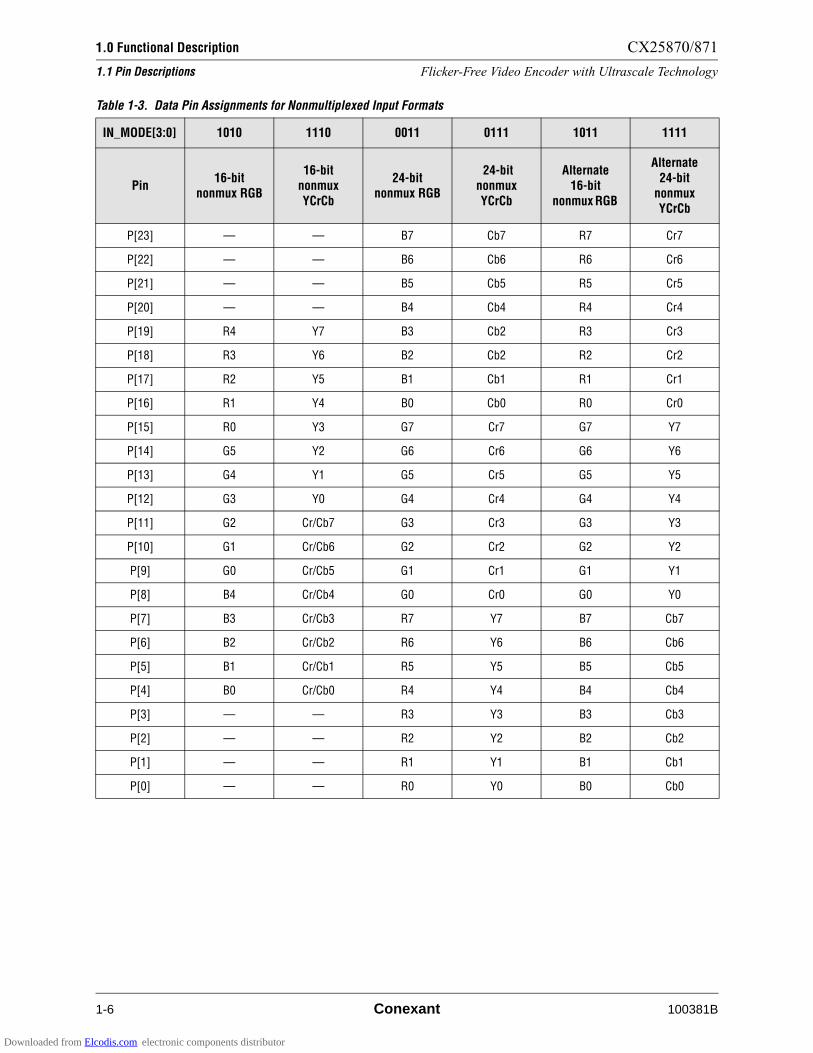
Table 1-3. Data Pin Assignments for Nonmultiplexed Input Formats
IN_MODE[3:0] 1010 1110 0011 0111 1011 1111
Pin16-bit
nonmux RGB
16-bit nonmux YCrCb
24-bit nonmux RGB
24-bit nonmux YCrCb
Alternate 16-bit
nonmux RGB
Alternate 24-bit
nonmux YCrCb
P[23] — — B7 Cb7 R7 Cr7
P[22] — — B6 Cb6 R6 Cr6
P[21] — — B5 Cb5 R5 Cr5
P[20] — — B4 Cb4 R4 Cr4
P[19] R4 Y7 B3 Cb2 R3 Cr3
P[18] R3 Y6 B2 Cb2 R2 Cr2
P[17] R2 Y5 B1 Cb1 R1 Cr1
P[16] R1 Y4 B0 Cb0 R0 Cr0
P[15] R0 Y3 G7 Cr7 G7 Y7
P[14] G5 Y2 G6 Cr6 G6 Y6
P[13] G4 Y1 G5 Cr5 G5 Y5
P[12] G3 Y0 G4 Cr4 G4 Y4
P[11] G2 Cr/Cb7 G3 Cr3 G3 Y3
P[10] G1 Cr/Cb6 G2 Cr2 G2 Y2
P[9] G0 Cr/Cb5 G1 Cr1 G1 Y1
P[8] B4 Cr/Cb4 G0 Cr0 G0 Y0
P[7] B3 Cr/Cb3 R7 Y7 B7 Cb7
P[6] B2 Cr/Cb2 R6 Y6 B6 Cb6
P[5] B1 Cr/Cb1 R5 Y5 B5 Cb5
P[4] B0 Cr/Cb0 R4 Y4 B4 Cb4
P[3] — — R3 Y3 B3 Cb3
P[2] — — R2 Y2 B2 Cb2
P[1] — — R1 Y1 B1 Cb1
P[0] — — R0 Y0 B0 Cb0
Downloaded from Elcodis.com electronic components distributor
CX25870/871 1.0 Functional Description
Flicker-Free Video Encoder with Ultrascale Technology 1.2 GUI Controller Programmability and Frequency Requirement
100381B Conexant 1-7
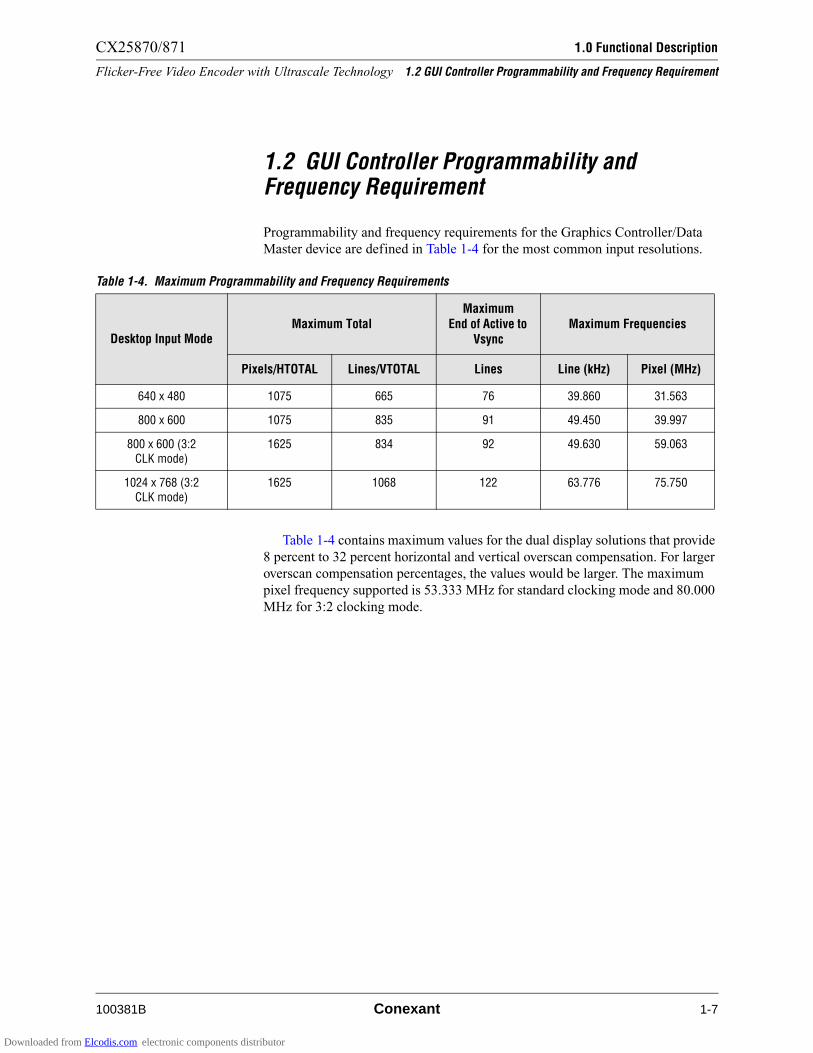
1.2 GUI Controller Programmability and Frequency Requirement
Programmability and frequency requirements for the Graphics Controller/Data
Master device are defined in Table 1-4 for the most common input resolutions.
Table 1-4 contains maximum values for the dual display solutions that provide
8 percent to 32 percent horizontal and vertical overscan compensation. For larger
overscan compensation percentages, the values would be larger. The maximum
pixel frequency supported is 53.333 MHz for standard clocking mode and 80.000
MHz for 3:2 clocking mode.
Table 1-4. Maximum Programmability and Frequency Requirements
Desktop Input ModeMaximum Total
MaximumEnd of Active to
VsyncMaximum Frequencies
Pixels/HTOTAL Lines/VTOTAL Lines Line (kHz) Pixel (MHz)
640 x 480 1075 665 76 39.860 31.563
800 x 600 1075 835 91 49.450 39.997
800 x 600 (3:2 CLK mode)
1625 834 92 49.630 59.063
1024 x 768 (3:2 CLK mode)
1625 1068 122 63.776 75.750
Downloaded from Elcodis.com electronic components distributor

1.0 Functional Description CX25870/871
1.2 GUI Controller Programmability and Frequency Requirement Flicker-Free Video Encoder with Ultrascale Technology
1-8 Conexant 100381B
Figure 1-2. Flicker Filter Control Diagram
Inpu
t
IN_M
OD
E[3
:0]
0000
= 2
4-bi
t R
GB
Mux
AD
PT
_FF
= 0
;F
_SE
LY[2
:0]
000
= 5
Lin
e
001
= 2
Lin
e
011
= 4
Lin
e
100
= A
lt. 5
Lin
e 1
AD
PT
_FF
= 0
;F
_SE
LC[2
:0]
000
= 5
Lin
e
001
= 2
Lin
e
100
= A
lt. 5
Lin
e 1
111
= A
lt. 5
Lin
e 4
DIS
_GM
SH
YY
LPF
[1:0
]
00 =
Byp
ass
01 =
Lum
a,H
oriz
onta
lLP
F1
YAT
TE
NU
ATE
[2:0
]
000
= 1
.0 G
ain
001
= 1
5/16
Gai
n
010
= 7
/8 G
ain
011
= 3
/4 G
ain
100
= 1
/2 G
ain
CAT
TE
NU
ATE
[2:0
]
000
= 1
.0 G
ain
001
= 1
5/16
Gai
n
010
= 7
/8 G
ain
011
= 3
/4 G
ain
Flic
ker
Filt
er/S
cale
r
0 =
Ena
ble
Lum
aP
sued
o G
amm
aR
emov
al00
01 =
16-
bit
RG
B M
ux
1010
= 1
6-bi
t R
GB
Non
-Mux
0010
= 1
5-bi
t R
GB
Mux
0011
= 2
4-bi
t R
GB
Non
-Mux
0101
= 1
6-bi
t Y
CrC
b M
ux
0110
= A
ltern
ate
16-b
itY
CrC
b M
ux
10 =
Lum
a,H
oriz
onta
lLP
F2
11 =
Lum
a,H
oriz
onta
lLP
F3
CLP
F[1
:0]
00 =
Byp
ass
01 =
Res
erve
d
10 =
Chr
oma,
Hor
izon
tal
LPF
2
11 =
Chr
oma,
Hor
izon
tal
LPF
3
YC
OR
ING
[2:0
]
001
= 1
/128
of R
ange
010
= 1
/64
of R
ange
011
= 1
/32
of R
ange
100
= 1
/16
of R
ange
101
= 1
/8of
Ran
ge11
0 =
1/4
of R
ange
111
= R
eser
ved
DIS
_GM
SH
C
0 =
Ena
ble
Chr
oma
Psu
edo
Gam
ma
Rem
oval
DIS
_GM
US
HY
0 =
Ena
ble
Lum
aA
nti-P
seud
o G
amm
aR
emov
al
DIS
_GM
US
HC
0 =
Ena
ble
Chr
oma
Ant
i-Psu
edo
Gam
ma
Rem
oval
DIS
_YF
LPF
0 =
Ena
ble
Initi
alLu
ma
Hor
izon
tal
Low
Pas
sF
ilter
CC
OR
ING
[2:0
]
001
= +
/-1/
256
of R
ange
010
= +
/- 1
/128
of R
ange
011
= +
/- 1
/64
of R
ange
100
= +
/- 1
/32
of R
ange
101
= +
/- 1
/16
of R
ange
110
= +
/- 1
/8of
Ran
ge11
1 =
Res
erve
d
000
= B
ypas
s
000
= B
ypas
s
0111
= 2
4-bi
t Y
CrC
b N
on-M
ux
1110
= 1
6-bi
t Y
CrC
b N
on-M
ux
0100
= 2
4-bi
tY
CrC
b M
ux
1000
= A
ltern
ate
24-b
itR
GB
Mux
1100
= A
ltern
ate
24-b
itY
CrC
b M
ux
1001
= R
eser
ved
1101
= R
eser
ved
1011
= A
ltern
ate
24-b
it R
GB
Non
-Mux
1111
= A
ltern
ate
24-b
it R
GB
Non
-Mux
Col
orS
pace
Con
vert
er
100381_003
FIF
O
111
= A
lt. 5
Lin
e 4
110
= A
lt. 5
Lin
e 3
101
= A
lt. 5
Lin
e 2
011
= 4
Lin
e
010
= 3
Lin
e
110
= A
lt. 5
Lin
e 3
101
= A
lt. 5
Lin
e 2
AD
PT
_FF
= 1
;Y
_AT
LFF
[1:0
]
00 =
5 L
ine
01 =
2 L
ine
11 =
4 L
ine
10 =
3 L
ine
AD
PT
_FF
= 1
;C
_AT
LFF
[1:0
]
00 =
5 L
ine
01 =
2 L
ine
11 =
4 L
ine
10 =
3 L
ine
111
= 0
.0 G
ain
110
= 1
/8 G
ain
101
= 1
/4 G
ain
111
= 0
.0 G
ain
110
= 1
/8 G
ain
101
= 1
/4 G
ain
100
= 1
/2 G
ain
010
= 3
Lin
e
Downloaded from Elcodis.com electronic components distributor

CX25870/871 1.0 Functional Description
Flicker-Free Video Encoder with Ultrascale Technology 1.2 GUI Controller Programmability and Frequency Requirement
100381B Conexant 1-9
Figure 1-3. CX25870/871 Encoder Core Block Diagram
100381_004
Inte
rnal
Vol
tage
Ref
eren
ce
FS
AD
JUS
T
DA
CA
Vid
eoT
imin
gC
ontr
ol,
SID
Reg
iste
rs
SIC
SID
RE
SE
T*
10
CO
MP
DA
CB
10
DA
CC
DA
CD
10 10
Out
Mux
Out
Mod
e
24R
GB
/Y
CR
CB
/Y
PR
PB
Y[9
:0]
CR
CB
[9:0
]
DA
C
DA
C
DA
C
DA
C
VB
IAS
+
Syn
cP
roce
ssor
+
1.3
MH
z LP
Fan
d 2X
Ups
ampl
e/M
atrix
Mul
tiplic
atio
n
Mod
ulat
or,
Mix
er a
ndS
EC
AM
Filt
.
HD
TV
Syn
cG
en.
10
Col
orS
pace
Con
vert
Clo
sed
Cap
tioni
ng,
Mac
rovi
sion
VR
EF
Lum
aD
elay
9
Lum
inan
ce2x
Ups
ampl
ean
dC
ross
Col
orP
eaki
ng F
ilt.
CG
MS
+
Y
CV
BS
U/V
RG
B
CV
BS C
DLY
SY
NC
_AM
P
MY
Bur
stP
roce
ssor
BS
T_A
MP
HU
E_O
FF
MC
R
HS
YN
C*
VS
YN
C*
MC
B
X
X
Downloaded from Elcodis.com electronic components distributor
1.0 Functional Description CX25870/871
1.3 Device Description Flicker-Free Video Encoder with Ultrascale Technology
1-10 Conexant 100381B
1.3 Device Description
1.3.1 Overview
The CX25870/871 is a video encoder designed for TV output of interlaced and
noninterlaced graphics data. Common applications requiring flicker-filtered TV
output include:
• desktop/portable PCs with TV Out
• high definition TVs
• DVD players and set top boxes
• graphic cards with TV Out
• game consoles
• set-top boxes
It incorporates normal and adaptive filtering technology for flicker removal
and flexible amounts of overscan compensation for high-quality display of
noninterlaced images on an interlaced TV. The CX25870/871 accomplishes this
by minimizing the flicker and controlling the amount of overscan so that the
entire image is viewable.
The CX25870/871 consists of a Color Space Converter/Flicker Filter engine
followed by a digital video encoder. The Color Space Converter/Flicker Filter
contains:
• A timing converter
• Various horizontal video processing functions
• Flicker filter and vertical scaler for overscan compensation
The output of this engine feeds into a FIFO for synchronization with the
digital video encoder.
The CX25870/871 provides Composite, S-Video, or 3-signal analog RGB or
YPBPR HDTV output. While the encoder is in HDTV output mode, the device
will automatically insert trilevel synchronization pulses (when necessary) and
vertical synchronizing “broad pulses.” The CX25870/871 is compliant with
EIA770-3, SMPTE 274M/293M/296M and supports ATSC HDTV resolutions
including 480p, 720p, and 1080i.
1.3.2 Serial Interface
The device includes a 2-wire read and write serial interface for programming the
registers in the device. The interface is designed to operate with 3.3 V levels. To
ensure that valid serial data is received and transmitted, make sure the VDD_SI
pin is connected to a stable 3.3 V supply. Review Chapter 2.2, Chapter 2.3 and
Chapter 2.4 for more details of the encoder’s serial interface.
Downloaded from Elcodis.com electronic components distributor
CX25870/871 1.0 Functional Description
Flicker-Free Video Encoder with Ultrascale Technology 1.3 Device Description
100381B Conexant 1-11
1.3.3 Low Voltage Graphics Interface
The CX25870/871 can receive or transmit signals from/to a graphics controller at
any of five different voltage levels. The allowable voltage levels are 3.3 V, 1.8 V,
1.5 V, 1.3 V, and 1.1 V. Default input/output voltage amplitude for the interface
signals (defined as P[23:0], HSYNC*, VSYNC*, CLKI, CLKO, BLANK*, and
FIELD) is 3.3 V and matches the Bt868/869 to ensure backwards compatibility.
For a 3.3 V digital interface, no special configuration steps are necessary.
Simply follow “Recommended Layout for Connection with a 3.3 V Master
Device” in Chapter 3.3 and on power-up, the encoder will automatically expect
3.3 V signal transitions.
For a 1.8 V or lower digital interface, several special configuration steps are
necessary. First, the layout must adhere to Chapter 3.3’s “3.3 V/1.8 V.
Recommended Layout for Connection with a 1.8 V Master Device.” Second,
program the DRVS[1:0] field (bits[6:5] of register (0x32)) to 01(or an alternate
value for 1.5 V, 1.3 V or 1.1 V interface). This forces the encoder to increase its
drive strength on each interface signal used as an output in the interface. Third,
connect the VDDL (pin 40) and VDD_CO (pin 57) power supply pins to the
correct lower supply voltage (1.8 V or other). Fourth, using a voltage divider
circuit or some other method, tie the CX25870/871’s VDD_VREF input (pin 49)
to a level equal to (VDDL/ 2 ). Make sure this voltage source is stable since the
VDDL pin controls the output signal levels. The VDD_VREF pin dictates the
encoder threshold voltage received for the appropriate input signals. The third and
fourth steps are illustrated in Figure 3-5. Make sure the graphics controller is
configured to send and accept signals at the lower supply voltage.
Adjusting VDD_CO, VDDL and VDD_VREF appropriately controls the
input voltage levels for the digital input pins P[23:0], CLKI, and
HSYNC*/VSYNC*/BLANK* (in slave interface; EN_BLANKO = 0). Using the
DRVS[1:0] bits control the output voltage levels for the digital output pins CLKO,
FIELD, and HSYNC*/VSYNC*/BLANK* (in master or pseudo-master interface;
EN_BLANKO = 1). In this way, the digital input pins can operate at different
input voltage levels than the digital output voltage levels.
Downloaded from Elcodis.com electronic components distributor
1.0 Functional Description CX25870/871
1.3 Device Description Flicker-Free Video Encoder with Ultrascale Technology
1-12 Conexant 100381B
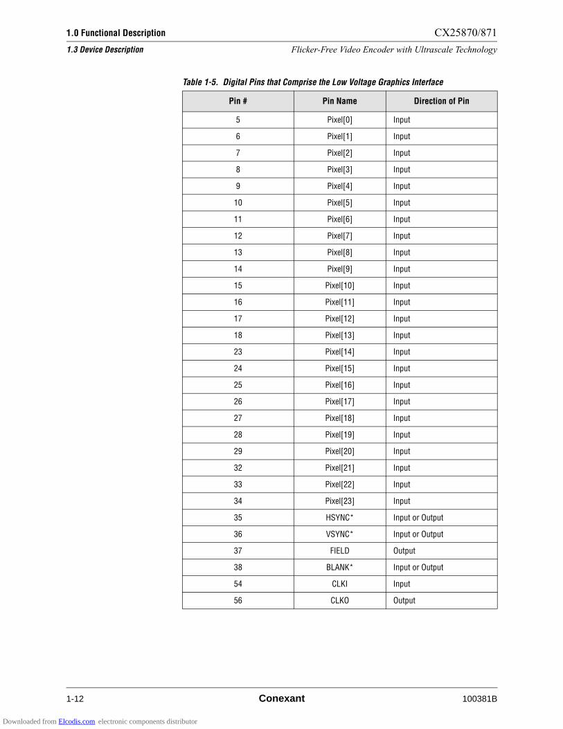
Table 1-5. Digital Pins that Comprise the Low Voltage Graphics Interface
Pin # Pin Name Direction of Pin
5 Pixel[0] Input
6 Pixel[1] Input
7 Pixel[2] Input
8 Pixel[3] Input
9 Pixel[4] Input
10 Pixel[5] Input
11 Pixel[6] Input
12 Pixel[7] Input
13 Pixel[8] Input
14 Pixel[9] Input
15 Pixel[10] Input
16 Pixel[11] Input
17 Pixel[12] Input
18 Pixel[13] Input
23 Pixel[14] Input
24 Pixel[15] Input
25 Pixel[16] Input
26 Pixel[17] Input
27 Pixel[18] Input
28 Pixel[19] Input
29 Pixel[20] Input
32 Pixel[21] Input
33 Pixel[22] Input
34 Pixel[23] Input
35 HSYNC* Input or Output
36 VSYNC* Input or Output
37 FIELD Output
38 BLANK* Input or Output
54 CLKI Input
56 CLKO Output
Downloaded from Elcodis.com electronic components distributor
CX25870/871 1.0 Functional Description
Flicker-Free Video Encoder with Ultrascale Technology 1.3 Device Description
100381B Conexant 1-13
1.3.4 Reset
If the RESET* pin is held low (between 0.8 V and GND –0.5 V) for a minimum
of 20 clock cycles, a timing reset and a software reset is performed and the serial
interface is held in the reset condition. A timing reset, which can be generated by
setting the TIMING_RST register bit, will set the subcarrier phase to zero, and
configure the horizontal and vertical counters to the beginning of VSYNC* of
Field 1 (both counters equal to zero).
If the CX25870/871 is in the master interface (i.e., CX25870 sends the syncs
to the data master) then after a power-on or pin reset the encoder and the flicker
filter starts a line 1, pixel 1 of their respective timing generation. For the encoder
this means the odd field is always the first field after a power-on reset, pin reset,
or timing reset.
In timing the slave interface (CX25870 is either pseudo-master or pure slave),
even though the input is receiving progressive frames that have no field
associated with it, the input timing generator keeps track of the frames received.
As a result, after every second frame received, a frame sync is sent to the encoder
section so that the input and encoder remain synchronized. The frame sync forces
the encoder to the beginning of the odd field.
Conexant recommends that after every overscan compensation or video output
type change, the TIMING_RST bit be enabled. The setting of the TIMING_RST
bit should occur after waiting a minimum of 1 ms between the last CX25870
register write for the new overscan compensation ratio. The TIMING_RST
register bit clears itself and reinitializes the internal timing generators.
A software reset, which can be generated by setting the SRESET register bit,
initializes all the serial interface registers to their default state. As a result, all
digital output control pins are three-stated. Registers 0x38 and 0x76 to 0xB4
inclusive are then initialized to auto-configuration mode 0 (see the Auto
Configuration section values) or mode 1 depending on the state of the PAL pin.
The EN_OUT bit must be set to enable the digital outputs.
A power-on reset, pin reset, or timing reset (register 0x6C, bit 7) causes the
input timing generator to send the encoder a frame synchronization pulse setting
the encoder to the beginning of the odd field. The first HSYNC*/VSYNC*
combination then corresponds to the encoder even field and then the second
HSYNC*/VSYNC* combination again causes a frame synchronization pulse and
the encoder will start the odd field, and so on and so forth.
A power-on reset is generated on power-up. The power-on reset generates the
same type of reset as the RESET* pin. A time delay circuit triggered after the
supply voltage reaches a value sufficiently high enough for the circuit to operate
and then generate the power-on reset. As such, the device may not initialize to the
default state unless the power supply ramp rate is sufficiently fast enough. A
hardware/pin reset is recommended if the default state is required.
1.3.5 Device Initialization
After a reset condition, the device must be programmed through the serial
interface to activate a video output and enable the CLKO, HSYNC*, VSYNC*,
and FIELD outputs. The easiest method for accomplishing the initialization phase
is to use one of the auto configuration modes in Appendix C, and program the
interface bits appropriately. (Refer to Section 1.3.8.)
Downloaded from Elcodis.com electronic components distributor

1.0 Functional Description CX25870/871
1.3 Device Description Flicker-Free Video Encoder with Ultrascale Technology
1-14 Conexant 100381B
1.3.6 Clocking and Timing Generation
Two timing generators control the operation of the encoder. The output encoder
timing block generates the signals for the proper encoding of the video into
NTSC, PAL, or SECAM and extracts the processed input pixels from the internal
FIFO. The encoding timing generator can receive its clock from either an external
crystal oscillator and internal PLL (master and pseudo-master interface), or from
the CLKI pin (slave interface). Conexant recommends that the encoding clock be
generated by the PLL. Register bit EX_XCLK selects the clock source. If
EN_XCLK is set to a logical 0, the internal clock source is selected via the crystal
attached to XTALIN/XTALOUT. When the EN_XCLK bit is set, the clock source
received at the CLKI pin is utilized as the main pixel/encoder clock. Conexant
recommends that the encoding clock be generated by the PLL.
A crystal must be present between XTALIN and XTALOUT pins if the
internal clock source is selected. In this case, the CX25870/871’s CLK frequency
is synthesized by its PLL such that the pixel clock frequency equals
For PLL DIV10=0: Fclk = Fxtal * PLL_INT(5:0) + [PLL_FRACT(15:0)/216]/6
For PLL DIV10=1: Fclk = Fxtal * PLL INT(5:0) + [PLL FRACT(15:0)/216]/10
where:
Fclk = CLKO Output Frequency = CLKI Input Frequency
NOTE: In some special modes, CLKO = Fclk / 2.
The crystal must be chosen so that the precise line rate for the video standards
required can be achieved. This is done to maintain the subcarrier relationship to
the line rate and thereby achieve the precise subcarrier frequency required. The
crystal oscillator is designed to oscillate from 5 MHz through 25 MHz. A
13.5000 MHz crystal meets the requirements for NTSC, PAL, and SECAM video
standards. The crystal must be within 50 ppm of the maximum desired clock rate
for NTSC operation, and 25 ppm for PAL or SECAM operation, across the
temperature range (0° to 70° C). If the CX25870/871 is to provide all video
outputs selectable through software, the customer must use a crystal with a
maximum tolerance across the temperature range of 25 ppm. Appendix B
contains a list of previously tested and recommended crystal vendors.
The crystal oscillator is disabled by the XTAL _PAD_DIS register bit.
Sufficient time (20 µs) must be allowed after coming out of sleep mode to allow
the oscillator to stabilize. The PLL_LOCK bit is set when the PLL is stable. In
addition, if the PLL_INPUT register bit is set to a logical 1, CLKI is selected as
the reference for PLL. In this special mode (slave interface with the PLL_32CLK
high), the above Fclk formulas replace Fxtal with FCLKI/2 (i.e., input clock
frequency is divided by 2).
If the external clock source is selected (EN_XCLK=1), a clock signal of the
desired pixel clock rate must be present at the CLKI pin. The CLKO pin is
three-stated, and the crystal oscillator disabled. The clock must meet the same
requirements as above. It is highly recommended that the internal clock be used in
order to ensure the output video remains within the specifications defined by the
relevant video standard. Any aberration in the source clock is reflected in the
color subcarrier frequency of the output video and detracts from the quality of the
image on the television.
Downloaded from Elcodis.com electronic components distributor
CX25870/871 1.0 Functional Description
Flicker-Free Video Encoder with Ultrascale Technology 1.3 Device Description
100381B Conexant 1-15
The BY_PLL bit bypasses the PLL, and the encoder clock will be at the
crystal frequency. This bit takes precedence over the EN_XCLK bit.
The second timing generator controls the generation of the HSYNC*,
VSYNC*, and BLANK* signals, and pixel input clocking. This is normally the
same clock as the encoding clock. The EN_ASYNC register bit, if set, allows this
clock to be driven directly by the CLKI pin. If the DIV2 register bit is set, this
internal clock is divided by two before driving the second timing generator. This
is required for interlaced input to interlaced output mode (i.e., CCIR601/DVD
and CCIR656 applications).
The CLKI pin is the clock used for synchronizing pixel inputs (P[23:0]) with
the timing input signals (HSYNC*, VSYNC*, and BLANK*) and normally is a
delayed version of the CLKO pin. It can be directly connected to CLKO if
desired. Data is registered with this input and re-synchronized to the internal
clock. In a multiplexed input mode, both edges of the CLKI input are used. If the
MODE2X register bit is set, the internal clock is divided by two, allowing a 2x
external clock, and data to be provided on the rising edge only.
1.3.6.1 3:2 ClockingMode
All graphics controllers require some finite time for resetting their internal
counters to zero, clearing register flags, and any other event that needs to be
performed on a line-by-line basis. The sum of time these incidents take are the
graphics controller’s Horizontal Blanking Time. The amount of Horizontal
Blanking time varies from one master device to another but it can never be less
than 0 µs and usually does not exceed 4 !s per digital line.
Downloaded from Elcodis.com electronic components distributor

1.0 Functional Description CX25870/871
1.3 Device Description Flicker-Free Video Encoder with Ultrascale Technology
1-16 Conexant 100381B
Figure 1-4 illustrates higher resolutions (i.e., 800x600 or greater), for some
data master devices that require more Horizontal Blanking Time than the
CX25870/871 provides in standard clocking mode, for dual display of certain
overscan compensation percentage pairs. For example, a graphics controller may
require a minimum total of 1.25 µs of Horizontal Blanking time per line while
clocking a frame with an active resolution of 800x600 to the encoder. If this were
the case, the entire set of overscan compensation solutions charted at the 1 µs
diagonal plot line (denoted with a dot-dash-dot) and below are made unavailable
to the designer. The result is a more limited set of overscan pairs to choose from,
and correspondingly less size control for the picture when displayed on a
television.
Figure 1-4. Allowable Overscan Compensation Ratios for Dual Display, 800x600 Input/NTSC Output
NOTE(S):Use this chart for PAL M and PAL 60 allowable overscan ratios
8 10 12 14 16 18 20 228
10
12
14
16
18
20
22
24
Vertical Overscan Compensation Percentage
Hor
izon
tal O
vers
can
Com
pens
atio
n P
erce
ntag
e
Overscan Compensation Percentage Pairs for 800x600 NTSC
0 µs Horizontal Blanking
1 µs
2 µs
3 µs
.75 µs
= Pixel Clock Solution
= 8-Cycle Character Clock Solution
= 9-Cycle Character Clock Solution
Legend:
Downloaded from Elcodis.com electronic components distributor
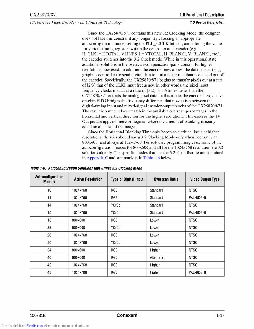
CX25870/871 1.0 Functional Description
Flicker-Free Video Encoder with Ultrascale Technology 1.3 Device Description
100381B Conexant 1-17
Since the CX25870/871 contains this new 3:2 Clocking Mode, the designer
does not face this constraint any longer. By choosing an appropriate
autoconfiguration mode, setting the PLL_32CLK bit to 1, and altering the values
for various timing registers within the controller and encoder (e.g.,
H_CLKI = HTOTAL, VLINES_I = VTOTAL, H_BLANKI, V_BLANKI, etc.),
the encoder switches into the 3:2 Clock mode. While in this operational state,
additional solutions in the overscan-compensation-pairs domain for higher
resolutions now exist. In addition, the encoder now allows the data master (e.g.,
graphics controller) to send digital data to it at a faster rate than is clocked out of
the encoder. Specifically, the CX25870/871 begins to transfer pixels out at a rate
of [2/3] that of the CLKI input frequency. In other words, the pixel input
frequency clocks in data at a ratio of [3:2] or 1½ times faster than the
CX25870/871 outputs the analog pixel data. In this mode, the encoder's expansive
on-chip FIFO bridges the frequency difference that now exists between the
digital-timing input and mixed-signal encoder output blocks of the CX25870/871.
The result is a much closer match in the available overscan percentages in the
horizontal and vertical direction for the higher resolutions. This ensures the TV
Out picture appears more orthogonal where the amount of blanking is nearly
equal on all sides of the image.
Since the Horizontal Blanking Time only becomes a critical issue at higher
resolutions, the user should use a 3:2 Clocking Mode only when necessary at
800x600, and always at 1024x768. For software programming ease, some of the
autoconfiguration modes for 800x600 and all for the 1024x768 resolution are 3:2
solutions already. The specific modes that use the 3:2 clock feature are contained
in Appendix C and summarized in Table 1-6 below.
Table 1-6. Autoconfiguration Solutions that Utilize 3:2 Clocking Mode
Autoconfiguration
Mode #Active Resolution Type of Digital Input Overscan Ratio Video Output Type
10 1024x768 RGB Standard NTSC
11 1024x768 RGB Standard PAL-BDGHI
14 1024x768 YCrCb Standard NTSC
15 1024x768 YCrCb Standard PAL-BDGHI
18 800x600 RGB Lower NTSC
22 800x600 YCrCb Lower NTSC
26 1024x768 RGB Lower NTSC
30 1024x768 YCrCb Lower NTSC
34 800x600 RGB Higher NTSC
40 800x600 RGB Alternate NTSC
42 1024x768 RGB Higher NTSC
43 1024x768 RGB Higher PAL-BDGHI
Downloaded from Elcodis.com electronic components distributor
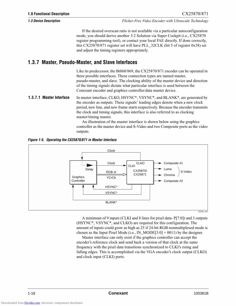
1.0 Functional Description CX25870/871
1.3 Device Description Flicker-Free Video Encoder with Ultrascale Technology
1-18 Conexant 100381B
If the desired overscan ratio is not available via a particular autoconfiguration
mode, you should derive another 3:2 Solution via Super Cockpit (i.e., CX25870
register programming tool), or contact your local FAE directly. If done correctly,
this CX25870/871 register set will have PLL_32CLK (bit 5 of register 0x38) set
and adjust the timing registers appropriately.
1.3.7 Master, Pseudo-Master, and Slave Interfaces
Like its predecessor, the Bt868/869, the CX25870/871 encoder can be operated in
three possible interfaces. These connection types are named master,
pseudo-master, and slave. The clocking ability of the master device and direction
of the timing signals dictate what particular interface is used between the
Conexant encoder and graphics controller/data master device.
1.3.7.1 Master Interface In master interface, CLKO, HSYNC*, VSYNC*, and BLANK*, are generated by
the encoder as outputs. These signals’ leading edges denote when a new clock
period, new line, and new frame starts respectively. Because the encoder transmits
the clock and timing signals, this interface is also referred to as clocking
master/timing master.
An illustration of the master interface is shown below using the graphics
controller as the master device and S-Video and two Composite ports as the video
outputs.
A minimum of 9 inputs (CLKI and 8 lines for pixel data- P[7:0]) and 3 outputs
(HSYNC*, VSYNC*, and CLKO) are required for this configuration. The
amount of inputs could grow as high as 25 if 24-bit RGB nonmultiplexed mode is
chosen as the Input Pixel Mode (i.e., IN_MODE[3:0] = 0011) by the designer.
Master interface can only exist if the graphics controller can accept the
encoder’s reference clock and send back a version of that clock at the same
frequency with the pixel data transitions synchronized to CLKI’s rising and
falling edges. This is accomplished via the VGA encoder’s clock output (CLKO)
and clock input (CLKI) ports.
Figure 1-5. Operating the CX25870/871 in Master Interface
GraphicsController
RGB or
YCrCb
Clock
CLKOCLKI
Clock
CX25870/CX25871
Composite #1
Composite #2
S-VideoLuma
Chroma
Delay
HSYNC*
VSYNC*
BLANK*
100381_054
Downloaded from Elcodis.com electronic components distributor

CX25870/871 1.0 Functional Description
Flicker-Free Video Encoder with Ultrascale Technology 1.3 Device Description
100381B Conexant 1-19
1.3.7.2 Reason forBLANK*
If the graphics controller possesses pixel-based resolution (i.e., pixels are only a
single pixel clock wide) then the encoder does not have to transmit or receive the
BLANK* signal. However, for graphics controllers that are character clock based,
a BLANK* signal is necessary.
The BLANK line is necessary because a character clock is actually 8 or 9
pixel clocks in duration. This causes several pixel clocks to elapse, resulting in an
erroneous delay prior to the next HSYNC* being observed by the encoder and the
next line starting. The only method of compensating for this delay is for character
clock based controllers to use the BLANK* signal. This signal is required in the
physical interface to indicate the exact location of the first active pixel on each
line.
1.3.7.3 Pseudo-MasterInterface
In pseudo-master interface, the CX25870/871 generates clock reference signal,
CLKO as an output. This signal’s purpose is to inform the graphics controller the
exact frequency at which the data must be sent to the encoder. Timing signals,
HSYNC*, VSYNC*, and BLANK*, are received by the encoder as inputs. The
leading edges of these signals denote when a new clock period, new line, and new
frame starts, respectively. Because this connection scheme shares mastering
responsibilities, the interface is also named clocking master/timing slave.
An illustration of the pseudo-master interface is illustrated below using the
graphics controller as the timing master device.
A minimum of 11 inputs (CLKI, HSYNC*, VSYNC*, and 8 lines for pixel
data- P[7:0]) and 1 output (CLKO) are required for this configuration. The
amount of inputs could grow as high as 28 if 24-bit RGB nonmultiplexed mode is
chosen as the Input Pixel Mode (i.e., IN_MODE[3:0] = 0111) by the designer.
Pseudo-Master interface can only exist if the graphics controller can accept
the encoder’s reference clock and send back a version of that clock at the same
frequency with the pixel data transitions synchronized to CLKI’s rising and
falling edges. This is accomplished via the VGA encoder’s clock output (CLKO)
and clock input (CLKI) ports.
Figure 1-6. Operating the CX25870/871 in Pseudo-Master Interface
GraphicsController
RGB or
YCrCb
Clock
CLKOCLKI
Clock
CX25870/CX25871
Composite #1
Composite #2
Luma
Chroma
Delay
HSYNC*
VSYNC*
BLANK*
100381_055
Downloaded from Elcodis.com electronic components distributor
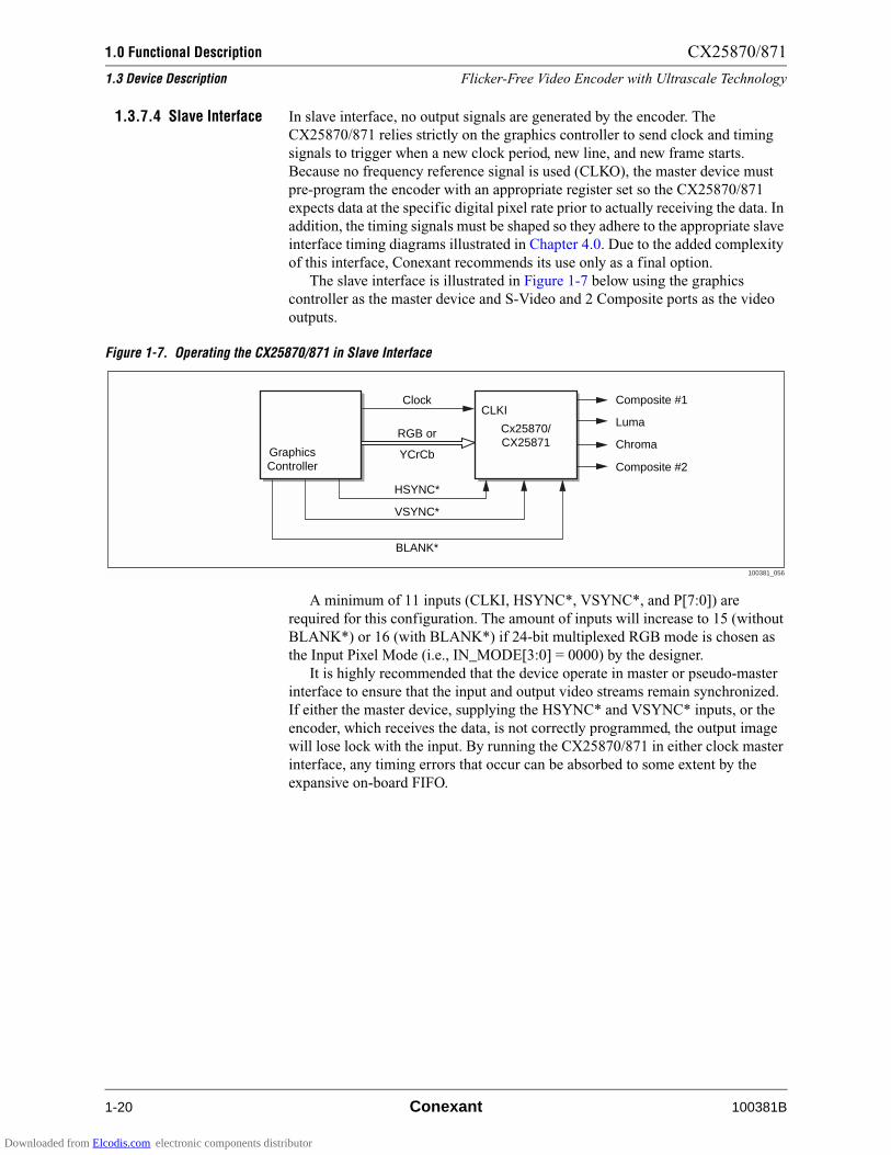
1.0 Functional Description CX25870/871
1.3 Device Description Flicker-Free Video Encoder with Ultrascale Technology
1-20 Conexant 100381B
1.3.7.4 Slave Interface In slave interface, no output signals are generated by the encoder. The
CX25870/871 relies strictly on the graphics controller to send clock and timing
signals to trigger when a new clock period, new line, and new frame starts.
Because no frequency reference signal is used (CLKO), the master device must
pre-program the encoder with an appropriate register set so the CX25870/871
expects data at the specific digital pixel rate prior to actually receiving the data. In
addition, the timing signals must be shaped so they adhere to the appropriate slave
interface timing diagrams illustrated in Chapter 4.0. Due to the added complexity
of this interface, Conexant recommends its use only as a final option.
The slave interface is illustrated in Figure 1-7 below using the graphics
controller as the master device and S-Video and 2 Composite ports as the video
outputs.
A minimum of 11 inputs (CLKI, HSYNC*, VSYNC*, and P[7:0]) are
required for this configuration. The amount of inputs will increase to 15 (without
BLANK*) or 16 (with BLANK*) if 24-bit multiplexed RGB mode is chosen as
the Input Pixel Mode (i.e., IN_MODE[3:0] = 0000) by the designer.
It is highly recommended that the device operate in master or pseudo-master
interface to ensure that the input and output video streams remain synchronized.
If either the master device, supplying the HSYNC* and VSYNC* inputs, or the
encoder, which receives the data, is not correctly programmed, the output image
will lose lock with the input. By running the CX25870/871 in either clock master
interface, any timing errors that occur can be absorbed to some extent by the
expansive on-board FIFO.
Figure 1-7. Operating the CX25870/871 in Slave Interface
GraphicsController
RGB or
YCrCb
CLKIClock
Cx25870/CX25871
Composite #1
Composite #2
Luma
Chroma
HSYNC*
VSYNC*
BLANK*
100381_056
Downloaded from Elcodis.com electronic components distributor

CX25870/871 1.0 Functional Description
Flicker-Free Video Encoder with Ultrascale Technology 1.3 Device Description
100381B Conexant 1-21
1.3.7.5 Slave InterfaceWithout a Crystal
For price-sensitive applications, it is possible to remove the crystal found between
the XTALIN and XTALOUT ports and strictly utilize the incoming CLKI signal
as both the data transfer mechanism and internal main clock source for the
encoder. To complete this architecture, the data master must also program the
CX25870’s EN_XCLK bit to 1. This will trigger CLKI to be used for all
operations requiring a clock source and force the encoder to ignore any
oscillations received via its XTALIN and XTALOUT pins. The flicker filter and
timing blocks will utilize this asynchronous clock on the input side for data
processing, and the encoder will combine its internal PLL and CLKI in
conjunction with the DACs to transmit video from the device.
Since CLKI will be the only incoming frequency reference, the encoder uses
this signal to run its internal PLL for derivation of the video color subcarrier
(Fsc). Since PAL and SECAM televisions are not lenient in accepting color
subcarrier frequencies with more than 25 ppm error (i.e., Fsc ± 330 Hz), it is
critical the data master maintain a very high level of accuracy for the incoming
clock. In numerical terms, this means that the incoming clock should always
remain within a window of ideal CLKI ± 25 ppm. As an example, for
autoconfiguration mode #1, CLKI would have to reside in the range
[29.499270 MHz < ideal CLKI = 29.500008 MHz < 29.500746 MHz.]
Tight control of the incoming digital clock ensures that the CX25870
generates an analog Fsc of 4.433618 MHz ± 338 Hz for PAL-BGHI or 4.250000 /
4.406250 MHz ± 338 Hz for SECAM. Actual testing has found that excursions
outside this range result in loss of color for PAL and SECAM televisions and
sometimes affect NTSC sets in the same manner.
When the CX25870 is receiving an external clock, its serial bus is also
dependent on this incoming signal. As a result, the data master should never
disable the input clock. If this happens, even momentarily, the only way the
encoder can recover is for the data master to pin RESET* the CX25870. The
encoder will then be re-enabled as a timing master and respond again to serial
commands transmitted by the data master.
Several other registers must be reprogrammed to make this special type of
interface work properly. Consult your local Conexant representative for technical
assistance.
Downloaded from Elcodis.com electronic components distributor
1.0 Functional Description CX25870/871
1.3 Device Description Flicker-Free Video Encoder with Ultrascale Technology
1-22 Conexant 100381B
1.3.8 Autoconfiguration and Interface Bits
The default operation of the CX25870/871 is tied into its 44 autoconfiguration
modes. Autoconfiguring the device occurs when bits CONFIG[5:3] and
CONFIG[2:0] in register 0xB8 are programmed to any state from 000000 to
101111. At the conclusion of this serial write, default values are copied from the
CX25870/871’s internal ROM into the most important timing registers that have
the indices 0x38 and 0x76 to 0xB4, inclusive. All other registers are not changed
at the conclusion of an autoconfiguration mode.
After an autoconfiguration command, the CX25870/871 device remains in the
same interface it was in before the command execution. Depending on which
autoconfiguration mode# was initiated, the CX25870/871 will expect to receive
either a 320x200, 320x240, 640x400, 640x480, 720x400, 720x480, 720x576,
800x600, or 1024x768 active digital input frame and output a NTSC or a PAL
composite and/or S-video signal. See Table 2-5 of this data sheet for a description
of CONFIG[5:0] and Appendix C for more detail on each autoconfiguration
mode.
Using an autoconfiguration mode is the easiest method for bringing up the
most popular desktop, game/Direct X, DOS boot-up screen, and DVD resolutions
with the encoder as both the timing and clock master. This is true even if the
graphics controller cannot utilize the CX25870/871 in master mode but must use
pseudo-master mode. To turn the direction of the SYNCs around so they are
transmitted by the graphics controller and received by the CX25870/871 simply
requires reprogramming the encoder via several serial writes.
The Interface bits that need to be changed are SLAVER, EN_BLANKO,
EN_DOT, and EN_OUT. Since the abilities of graphics controllers vary greatly,
Tables 1-7 through 1-12 have been compiled below to explain the relationship
between the Interface bits and the actual interface itself. Even more permutations
of the following interfaces below are possible but Tables 1-7 to 1-12 capture the
six most popular architectures.
Table 1-7. Master Interface without a BLANK* Signal (Default Immediately after any Autoconfiguration Command)
Interfaced UsedSLAVER (Bit 5 of 0xBA) ORed with
Slave Pin
EN_BLANKO (MSb of Register
0xC6)
EN_DOT (Bit 6 of Register
0xC6)
EN_OUT (LSb of Register
0xC4)
MASTER (default)
BLANK* is an output from the
CX25870/871 or BLANK* µs NOT
included as part of the interface.
0 1 0 1
Downloaded from Elcodis.com electronic components distributor
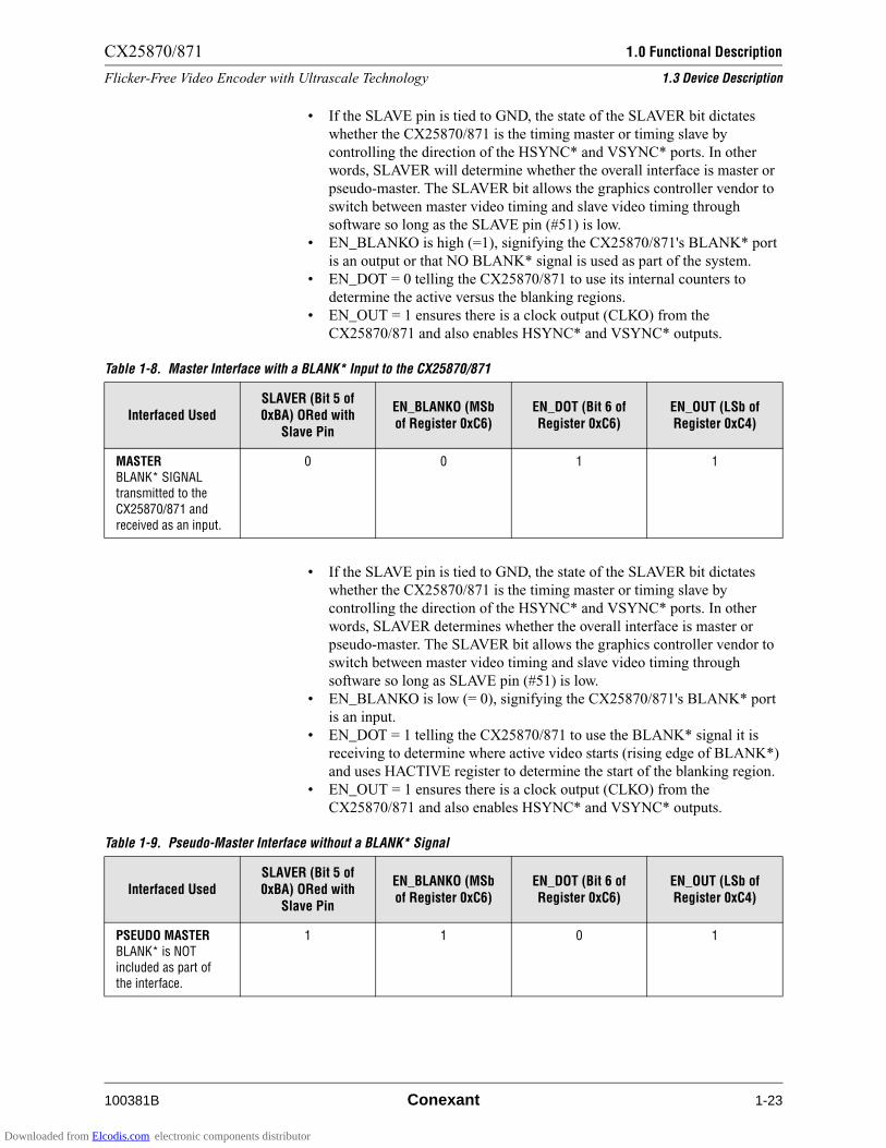
CX25870/871 1.0 Functional Description
Flicker-Free Video Encoder with Ultrascale Technology 1.3 Device Description
100381B Conexant 1-23
• If the SLAVE pin is tied to GND, the state of the SLAVER bit dictates
whether the CX25870/871 is the timing master or timing slave by
controlling the direction of the HSYNC* and VSYNC* ports. In other
words, SLAVER will determine whether the overall interface is master or
pseudo-master. The SLAVER bit allows the graphics controller vendor to
switch between master video timing and slave video timing through
software so long as the SLAVE pin (#51) is low.
• EN_BLANKO is high (=1), signifying the CX25870/871's BLANK* port
is an output or that NO BLANK* signal is used as part of the system.
• EN_DOT = 0 telling the CX25870/871 to use its internal counters to
determine the active versus the blanking regions.
• EN_OUT = 1 ensures there is a clock output (CLKO) from the
CX25870/871 and also enables HSYNC* and VSYNC* outputs.
• If the SLAVE pin is tied to GND, the state of the SLAVER bit dictates
whether the CX25870/871 is the timing master or timing slave by
controlling the direction of the HSYNC* and VSYNC* ports. In other
words, SLAVER determines whether the overall interface is master or
pseudo-master. The SLAVER bit allows the graphics controller vendor to
switch between master video timing and slave video timing through
software so long as SLAVE pin (#51) is low.
• EN_BLANKO is low (= 0), signifying the CX25870/871's BLANK* port
is an input.
• EN_DOT = 1 telling the CX25870/871 to use the BLANK* signal it is
receiving to determine where active video starts (rising edge of BLANK*)
and uses HACTIVE register to determine the start of the blanking region.
• EN_OUT = 1 ensures there is a clock output (CLKO) from the
CX25870/871 and also enables HSYNC* and VSYNC* outputs.
Table 1-8. Master Interface with a BLANK* Input to the CX25870/871
Interfaced UsedSLAVER (Bit 5 of 0xBA) ORed with
Slave Pin
EN_BLANKO (MSb of Register 0xC6)
EN_DOT (Bit 6 of Register 0xC6)
EN_OUT (LSb of Register 0xC4)
MASTERBLANK* SIGNAL transmitted to the
CX25870/871 and received as an input.
0 0 1 1
Table 1-9. Pseudo-Master Interface without a BLANK* Signal
Interfaced UsedSLAVER (Bit 5 of 0xBA) ORed with
Slave Pin
EN_BLANKO (MSb of Register 0xC6)
EN_DOT (Bit 6 of Register 0xC6)
EN_OUT (LSb of Register 0xC4)
PSEUDO MASTERBLANK* is NOT
included as part of the interface.
1 1 0 1
Downloaded from Elcodis.com electronic components distributor
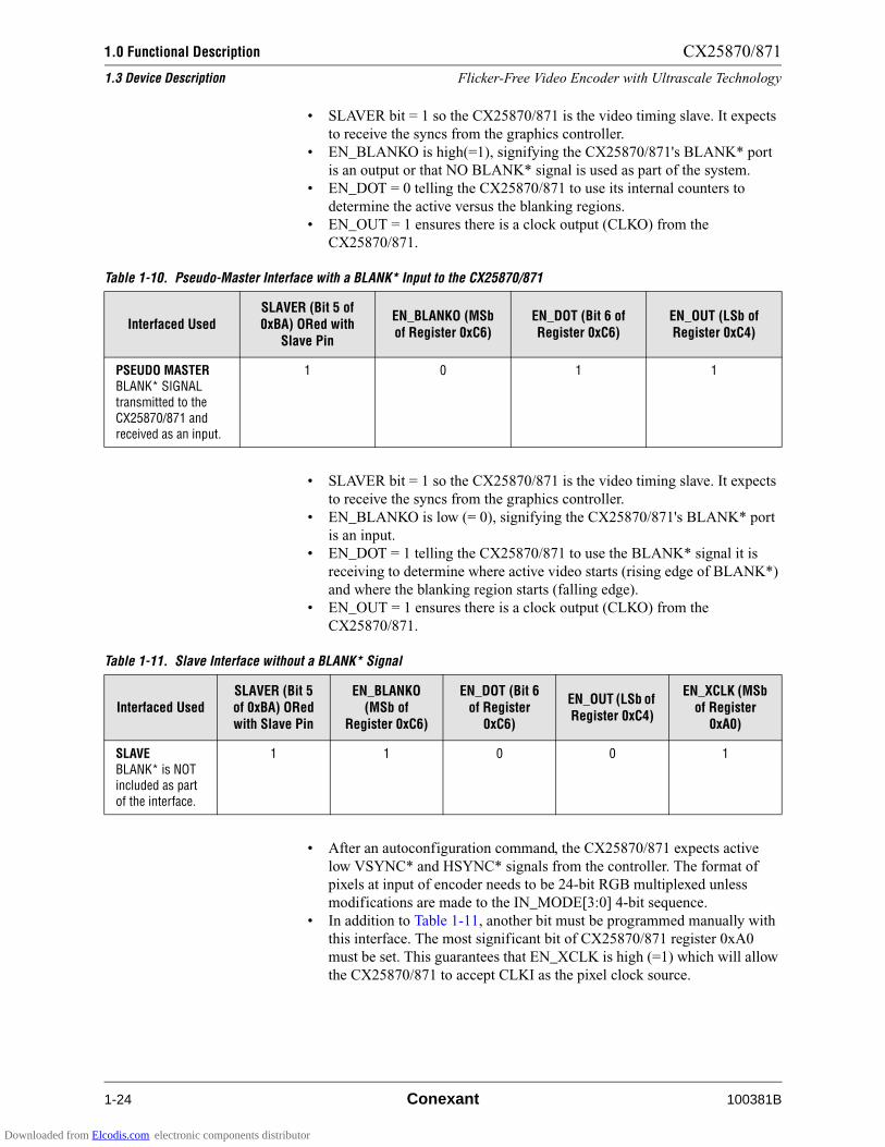
1.0 Functional Description CX25870/871
1.3 Device Description Flicker-Free Video Encoder with Ultrascale Technology
1-24 Conexant 100381B
• SLAVER bit = 1 so the CX25870/871 is the video timing slave. It expects
to receive the syncs from the graphics controller.
• EN_BLANKO is high(=1), signifying the CX25870/871's BLANK* port
is an output or that NO BLANK* signal is used as part of the system.
• EN_DOT = 0 telling the CX25870/871 to use its internal counters to
determine the active versus the blanking regions.
• EN_OUT = 1 ensures there is a clock output (CLKO) from the
CX25870/871.
• SLAVER bit = 1 so the CX25870/871 is the video timing slave. It expects
to receive the syncs from the graphics controller.
• EN_BLANKO is low (= 0), signifying the CX25870/871's BLANK* port
is an input.
• EN_DOT = 1 telling the CX25870/871 to use the BLANK* signal it is
receiving to determine where active video starts (rising edge of BLANK*)
and where the blanking region starts (falling edge).
• EN_OUT = 1 ensures there is a clock output (CLKO) from the
CX25870/871.
• After an autoconfiguration command, the CX25870/871 expects active
low VSYNC* and HSYNC* signals from the controller. The format of
pixels at input of encoder needs to be 24-bit RGB multiplexed unless
modifications are made to the IN_MODE[3:0] 4-bit sequence.
• In addition to Table 1-11, another bit must be programmed manually with
this interface. The most significant bit of CX25870/871 register 0xA0
must be set. This guarantees that EN_XCLK is high (=1) which will allow
the CX25870/871 to accept CLKI as the pixel clock source.
Table 1-10. Pseudo-Master Interface with a BLANK* Input to the CX25870/871
Interfaced UsedSLAVER (Bit 5 of 0xBA) ORed with
Slave Pin
EN_BLANKO (MSb of Register 0xC6)
EN_DOT (Bit 6 of Register 0xC6)
EN_OUT (LSb of Register 0xC4)
PSEUDO MASTERBLANK* SIGNAL
transmitted to the CX25870/871 and received as an input.
1 0 1 1
Table 1-11. Slave Interface without a BLANK* Signal
Interfaced UsedSLAVER (Bit 5 of 0xBA) ORed with Slave Pin
EN_BLANKO (MSb of
Register 0xC6)
EN_DOT (Bit 6 of Register
0xC6)
EN_OUT (LSb of Register 0xC4)
EN_XCLK (MSb of Register
0xA0)
SLAVEBLANK* is NOT included as part
of the interface.
1 1 0 0 1
Downloaded from Elcodis.com electronic components distributor

CX25870/871 1.0 Functional Description
Flicker-Free Video Encoder with Ultrascale Technology 1.3 Device Description
100381B Conexant 1-25
• SLAVER bit = 1 the CX25870/871 is the video timing slave. It expects to
receive the syncs from the graphics controller. Since the CX25870 is in
slave mode, the HSYNC* and VSYNC* outputs will be three-stated and
the CX25870/871 will be set up to receive these timing signals from the
graphics controller.
• EN_BLANKO is high (=1), signifying the CX25870/871's BLANK* port
is an output or that NO BLANK* signal is used as part of the system.
• EN_DOT = 0 telling the CX25870/871 to use its internal counters to
determine the active versus the blanking regions.
• EN_OUT = 0: This ensures the clock output port (CLKO) is three-stated
from the encoder.
• After an autoconfiguration command, the CX25870/871 expects active
low VSYNC* and HSYNC* signals from the controller. The format of
pixels at input of encoder needs to be 24-bit RGB multiplexed unless
modifications are made to the IN_MODE[3:0] 4-bit sequence.
• In addition to Table 1-11, another bit must be programmed manually with
this interface. The most significant bit of CX25870/871 register 0xA0
must be set. This guarantees that EN_XCLK will be high (=1) which will
allow the CX25870/871 to accept CLKI as the pixel clock source.
• SLAVER bit = 1 so the CX25870/871 is the video timing slave. It will
expect to receive the syncs from the graphics controller. Since the
CX25870 is in slave mode, then the HSYNC* and VSYNC* outputs will
be three-stated and the CX25870/871 will be set up to receive these timing
signals from the graphics controller.
• EN_BLANKO is low (= 0), signifying the CX25870/871's BLANK* port
is an input.
• EN_DOT = 1, telling the CX25870/871 to use the BLANK* signal it is
receiving to determine where active video starts (rising edge of BLANK*)
and the HACTIVE register to denote where the blanking region starts.
• EN_OUT = 0: This will ensure the clock output port (CLKO) is
three-stated from the encoder.
NOTE: Autoconfiguration Mode #28 and #29 for NTSC and PAL DVD Playback
place the encoder into slave interface where it expects a BLANK* input
(Table 1-11).
Table 1-12. Slave Interface with a BLANK* Input to the CX25870/871
Interfaced UsedSLAVER (Bit 5 of 0xBA) ORed with Slave Pin
EN_BLANKO (MSb of
Register 0xC6)
EN_DOT (Bit 6 of Register
0xC6)
EN_OUT (LSb of Register 0xC4)
EN_XCLK (MSb of Register
0xA0)
SLAVEBLANK* SIGNAL
transmitted to the CX25870/871 and received as
an input.
1 0 1 0 1
Downloaded from Elcodis.com electronic components distributor
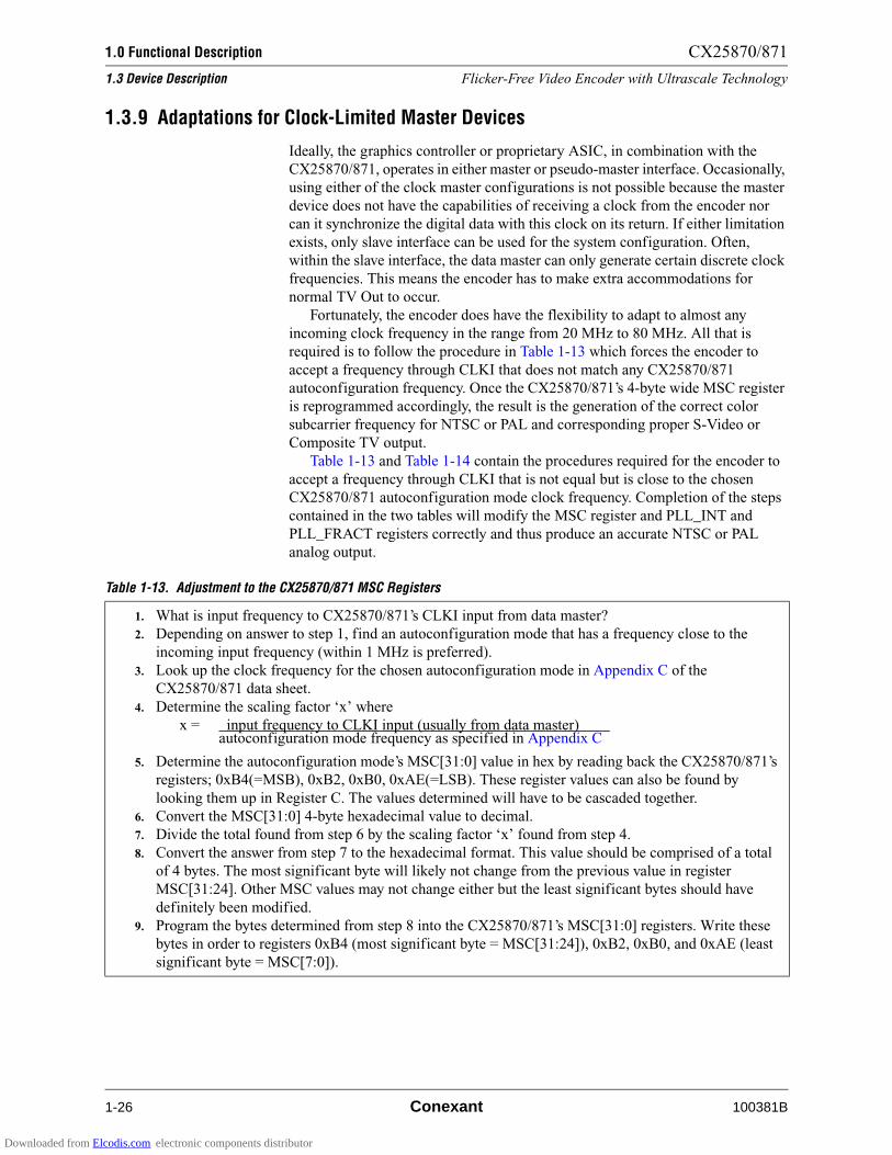
1.0 Functional Description CX25870/871
1.3 Device Description Flicker-Free Video Encoder with Ultrascale Technology
1-26 Conexant 100381B
1.3.9 Adaptations for Clock-Limited Master Devices
Ideally, the graphics controller or proprietary ASIC, in combination with the
CX25870/871, operates in either master or pseudo-master interface. Occasionally,
using either of the clock master configurations is not possible because the master
device does not have the capabilities of receiving a clock from the encoder nor
can it synchronize the digital data with this clock on its return. If either limitation
exists, only slave interface can be used for the system configuration. Often,
within the slave interface, the data master can only generate certain discrete clock
frequencies. This means the encoder has to make extra accommodations for
normal TV Out to occur.
Fortunately, the encoder does have the flexibility to adapt to almost any
incoming clock frequency in the range from 20 MHz to 80 MHz. All that is
required is to follow the procedure in Table 1-13 which forces the encoder to
accept a frequency through CLKI that does not match any CX25870/871
autoconfiguration frequency. Once the CX25870/871’s 4-byte wide MSC register
is reprogrammed accordingly, the result is the generation of the correct color
subcarrier frequency for NTSC or PAL and corresponding proper S-Video or
Composite TV output.
Table 1-13 and Table 1-14 contain the procedures required for the encoder to
accept a frequency through CLKI that is not equal but is close to the chosen
CX25870/871 autoconfiguration mode clock frequency. Completion of the steps
contained in the two tables will modify the MSC register and PLL_INT and
PLL_FRACT registers correctly and thus produce an accurate NTSC or PAL
analog output.
Table 1-13. Adjustment to the CX25870/871 MSC Registers
1. What is input frequency to CX25870/871’s CLKI input from data master?
2. Depending on answer to step 1, find an autoconfiguration mode that has a frequency close to the
incoming input frequency (within 1 MHz is preferred).
3. Look up the clock frequency for the chosen autoconfiguration mode in Appendix C of the
CX25870/871 data sheet.
4. Determine the scaling factor ‘x’ where
x = input frequency to CLKI input (usually from data master)autoconfiguration mode frequency as specified in Appendix C
5. Determine the autoconfiguration mode’s MSC[31:0] value in hex by reading back the CX25870/871’s
registers; 0xB4(=MSB), 0xB2, 0xB0, 0xAE(=LSB). These register values can also be found by
looking them up in Register C. The values determined will have to be cascaded together.
6. Convert the MSC[31:0] 4-byte hexadecimal value to decimal.
7. Divide the total found from step 6 by the scaling factor ‘x’ found from step 4.
8. Convert the answer from step 7 to the hexadecimal format. This value should be comprised of a total
of 4 bytes. The most significant byte will likely not change from the previous value in register
MSC[31:24]. Other MSC values may not change either but the least significant bytes should have
definitely been modified.
9. Program the bytes determined from step 8 into the CX25870/871’s MSC[31:0] registers. Write these
bytes in order to registers 0xB4 (most significant byte = MSC[31:24]), 0xB2, 0xB0, and 0xAE (least
significant byte = MSC[7:0]).
Downloaded from Elcodis.com electronic components distributor
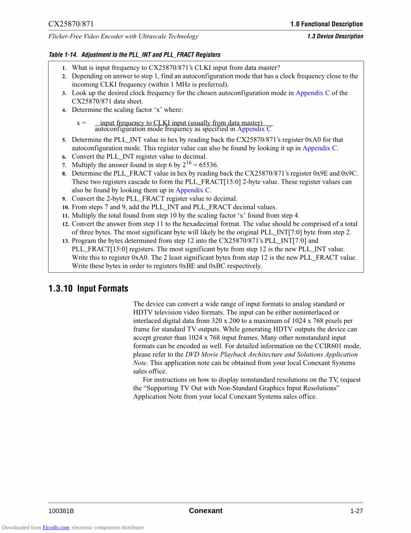
CX25870/871 1.0 Functional Description
Flicker-Free Video Encoder with Ultrascale Technology 1.3 Device Description
100381B Conexant 1-27
1.3.10 Input Formats
The device can convert a wide range of input formats to analog standard or
HDTV television video formats. The input can be either noninterlaced or
interlaced digital data from 320 x 200 to a maximum of 1024 x 768 pixels per
frame for standard TV outputs. While generating HDTV outputs the device can
accept greater than 1024 x 768 input frames. Many other nonstandard input
formats can be encoded as well. For detailed information on the CCIR601 mode,
please refer to the DVD Movie Playback Architecture and Solutions Application
Note. This application note can be obtained from your local Conexant Systems
sales office.
For instructions on how to display nonstandard resolutions on the TV, request
the “Supporting TV Out with Non-Standard Graphics Input Resolutions”
Application Note from your local Conexant Systems sales office.
Table 1-14. Adjustment to the PLL_INT and PLL_FRACT Registers
1. What is input frequency to CX25870/871’s CLKI input from data master?
2. Depending on answer to step 1, find an autoconfiguration mode that has a clock frequency close to the
incoming CLKI frequency (within 1 MHz is preferred).
3. Look up the desired clock frequency for the chosen autoconfiguration mode in Appendix C of the
CX25870/871 data sheet.
4. Determine the scaling factor ‘x’ where:
x = input frequency to CLKI input (usually from data master) autoconfiguration mode frequency as specified in Appendix C
5. Determine the PLL_INT value in hex by reading back the CX25870/871’s register 0xA0 for that
autoconfiguration mode. This register value can also be found by looking it up in Appendix C.
6. Convert the PLL_INT register value to decimal.
7. Multiply the answer found in step 6 by 216 = 65536.
8. Determine the PLL_FRACT value in hex by reading back the CX25870/871’s register 0x9E and 0x9C.
These two registers cascade to form the PLL_FRACT[15:0] 2-byte value. These register values can
also be found by looking them up in Appendix C.
9. Convert the 2-byte PLL_FRACT register value to decimal.
10. From steps 7 and 9, add the PLL_INT and PLL_FRACT decimal values.
11. Multiply the total found from step 10 by the scaling factor ‘x’ found from step 4.
12. Convert the answer from step 11 to the hexadecimal format. The value should be comprised of a total
of three bytes. The most significant byte will likely be the original PLL_INT[7:0] byte from step 2.
13. Program the bytes determined from step 12 into the CX25870/871’s PLL_INT[7:0] and
PLL_FRACT[15:0] registers. The most significant byte from step 12 is the new PLL_INT value.
Write this to register 0xA0. The 2 least significant bytes from step 12 is the new PLL_FRACT value.
Write these bytes in order to registers 0xBE and 0xBC respectively.
Downloaded from Elcodis.com electronic components distributor

1.0 Functional Description CX25870/871
1.3 Device Description Flicker-Free Video Encoder with Ultrascale Technology
1-28 Conexant 100381B
1.3.11 Input Pixel Timing
The device can accept the input data in either RGB or YCrCb color spaces. Data
can be input either a full pixel at a time clocked in on the rising edge of CLKI
only, or in various multiplexed modes, using both edges of CLKI.
In YCrCb format, either 24-bit 4:4:4 data or 16-bit 4:2:2 data can be input. In
RGB format, either 15-bit 5:5:5, 16 bit 5:6:5, or 24-bit RGB can be input. In
16-bit 4:2:2 YCrCb input format, multiplexed Y, Cr, and Cb data is input through
the P[11:4] or P[7:0]input pins. The Y data is input on the falling edge of CLKI.
The Cr/Cb data is input on the rising edge of CLKI. The Cb/Y/Cr/Y sequence
begins at the first active pixel. An additional 4:2:2 YCrCb input format maps Y to
P[19:12] and Cr/Cb multiplexed on P[11:4]. In 24-bit 4:4:4 YCrCb input format,
multiplexed Y, Cr, and Cb data is input through the P[11:0] inputs. Both the rising
and falling edge of CLKI sample the input data.
In RGB input format, input data is sampled as 12 bits at a time in 24-bit RGB
format or 8 bits at a time in 15/16 bit RGB format on both the rising and falling
edge of CLKI. Table 1-2 shows the data pin assignments for all available
multiplexed input formats.
In addition, all 24-bit formats, a 16-bit RGB format, and a 16-bit YCrCb
format can utilize the nonmultiplexed clocking method. See Table 1-3 for these
pin-to-bit assignments.
1.3.12 YCrCb Inputs (For Standard TV Outputs)
Y has a nominal range of 16–235; Cr and Cb have a nominal range of 16–240,
with 128 (80 hex) equal to zero. Values of 0 and 255 are interpreted as 1 and 254,
respectively. Y values of 1–15 and 236–254, and CrCb values of 1–15 and
241–254, are interpreted as valid linear values.
Downloaded from Elcodis.com electronic components distributor

CX25870/871 1.0 Functional Description
Flicker-Free Video Encoder with Ultrascale Technology 1.3 Device Description
100381B Conexant 1-29
Figure 1-8 illustrates the frequency response of the sub-sampling process. If
4:4:4 data is input, it is subsampled to 4:2:2 prior to overscan compensation and
flicker filtering.
The resulting 4:2:2 output must then be converted to YUV values and then
scaled for the output range of the DACs. The MY, MCR, and MCB registers must
be programmed to perform this conversion. The scaling equations are as follows:
MY = (int) [V100/(219.0 * VFS) * 26 + 0.5]
MCR = (int)[(128.0/127.0) * V100 * 0.877/(224.0 * VFS * 0.713 * sinx) * 26 + 0.5]
MCB = (int)[(128.0/127.0)* V100 * 0.493/(224.0 * VFS * 0.564 * sinx) * 26 + 0.5]
where:V100 = 100% white voltage (0.661 V for NTSC, 0.7 V for PAL/SECAM)
VFS = Full scale output voltage (1.28 V)
Fsc = color subcarrier frequency (see Table A-2)
Fclk = Analog pixel rate
Sinx = Sin ($#·FSC/FCLK)/($#·FSC/FCLK)
Figure 1-8. Decimation Filter at Fs=27 MHz
0
5
10
15
20
25
30
35
40
45
Frequency (Fs = 27 MHz)
Dec
ibel
s (d
B)
0 1 2 3 4 5 6
Chroma Decimation Filter
100381_005
Downloaded from Elcodis.com electronic components distributor
1.0 Functional Description CX25870/871
1.3 Device Description Flicker-Free Video Encoder with Ultrascale Technology
1-30 Conexant 100381B
1.3.13 RGB Inputs (For Standard TV Outputs)
With IN_MODE[3:0] set to a RGB mode, the encoder must receive digital
gamma-corrected RGB data as an input. If this occurs, the RGB data will be
converted to Y/R-Y/B-Y as follows:
Y[9:0] = [INT(0.299 * 210) * R[7:0] + INT(0.587 * 210 * G[7:0] + INT(0.114 *
210) * B[7:0] + 27] * 2-8
0 % Y[9:0] %#1024
For 15 and 16 bit RGB input formats, individual R, G, and B values are left
justified to eight bit numbers.
After the initial conversion, the Y/R-Y/B-Y values are sub-sampled to 4:2:2
data prior to overscan compensation and flicker filtering.
The resulting 4:2:2 output must then be converted to YUV values and then
scaled for the output range of the DACs. The MY, MCR, and MCB registers must
be programmed to perform this conversion. The scaling equations are:
MY = (int)[V100/(255 * VFS)*26 + 0.5]
MCR = (int)[(128.0/127.0) * V100 * 0.877/(127 * VFS * sinx) * 25 + 0.5]
MCB = (int)[(128.0/127.0) * V100 * 0.493/(127 * VFS * sinx) * 25 + 0.5]
where:V100 = 100% white voltage (0.661 V for NTSC, 0.7 V for PAL)
VFS = Full scale output voltage (1.28 V)
Fsc = color subcarrier frequency (see Table A-2)
Fclk = CLKI input frequency
Sinx = Sin [(2$#FSC/FCLK)/(2$#FSC/FCLK)]
For SECAM formulas see the SECAM section.
1.3.14 Input Pixel Horizontal Sync
The HSYNC* pin provides line synchronization for the pixel input data. It is an
output in master interface and an input in slave and pseudo-master interface. In
the master interface, it is a pulse two CLKI cycles in duration whose leading edge
indicates the beginning of a new line of pixel data. The period between two
consecutive HSYNC* pulses is H_CLKI CLK cycles. The first active pixel
should be presented to the device H_BLANKI minus the internal pipelined clock
(5 CLK cycles) after the leading edge of HSYNC*. The next H_ACTIVE pixels
are accepted as active pixels and used in the construction of the output video. In
the slave interface the exact number of clocks per line (H_CLKI) must be
provided as calculated for the desired overscan ratio. Only the leading edge of
HSYNC* is used, low times must be at least two CLKI cycles in duration.
HSYNC* is clocked into the encoder by the rising edge of CLKI.
The polarity of the HSYNC* signal is changed by the HSYNCI register bit.
The default convention is active low.
Downloaded from Elcodis.com electronic components distributor
CX25870/871 1.0 Functional Description
Flicker-Free Video Encoder with Ultrascale Technology 1.3 Device Description
100381B Conexant 1-31
1.3.15 Input Pixel Vertical Sync
The VSYNC* pin provides field synchronization for the pixel input data. It is an
output in master interface, and an input in the slave and the pseudo-master
interface.
For noninterlaced input timing in master interface, VSYNC* is a pulse one
horizontal line time in duration whose leading edge indicates the beginning of a
frame of input pixel data. The leading edge coincides with the leading edge of
HSYNC*. The period of the pulses is V_LINESI horizontal lines. The first line of
active data should be presented to the device V_BLANKI lines after the leading
edge of VSYNC*. The next V_ACTIVEI lines are accepted as active lines and
used in the construction of the output video.
The CX25870/871 disregards lines after the leading edge of VSYNC* but
before VSYNC* + V_BLANKI lines by not encoding them. In slave interface,
the period must be exactly the frame rate of the desired video format. Only the
leading edge is used, and the high and low duration must be at least two CLKI
cycles. The beginning of the frame of data is indicated by the next leading edge of
HSYNC* coincident with or after the leading edge of VSYNC*.
For interlaced input timing, only the slave interface is supported. The period
must be exactly the frame rate of the desired video format. If the leading edge of
HSYNC* and VSYNC* are coincident, that indicates the input is in odd field, the
internal line counter is reset to line 1 at the leading edge of VSYNC*. If the
leading edges of HSYNC* and VSYNC* are not coincident, and separated by a
minimum of two CLKI cycles, this indicates the input is an even field. In this
case, the internal line counter is reset to line 2 at the beginning of the next line.
Only the leading edge of VSYNC* is used, and the high and low VSYNC* width
must be at least two CLKI cycles. VSYNC* is clocked in by the rising edge of
CLKI.
The polarity of the VSYNC* input and output can be programmed by the
VSYNCI register bit. The default convention is active low. The FLD_MODE bits
allow further flexibility in HSYNC* and VSYNC* timing relationship.
1.3.16 Input Pixel Blanking
Input pixel blanking can be controlled by either the BLANK* pin or by the
internal registers. Blanking can be programmed independently of master or slave
interface using the EN_BLANKO register bit. As an output (EN_BLANKO = 1),
pixel blanking is generated based on the active area defined by H_BLANKI,
H_ACTIVE, V_BLANKI, and V_ACTIVEI registers. With EN_BLANKO = 1,
the BLANK* pin is output in the proper relationship to the syncs to indicate the
location of active pixels. As an input (EN_BLANKO = 0), when the BLANK* pin
goes high, it indicates the start of active pixels at the pixel input pins. In addition,
the H_BLANKI register must be programmed properly. The duration of active
data is still determined by the H_ACTIVE register. BLANK* is clocked by the
rising edge of CLKI.
An additional function for the BLANK* pin is used if the EN_DOT register
bit is set. If EN_DOT = 1, the BLANK* pin becomes an input whose rising edge
defines the graphics controller character clock boundary. This is used internally
by the encoder to keep track of the exact pixel count for controllers that cannot
operate at pixel clock rates but instead operate at VGA character clock rates.
The polarity of the BLANK* input/output can be programmed by the
BLANKI register bit. The default convention is active low.
Downloaded from Elcodis.com electronic components distributor
1.0 Functional Description CX25870/871
1.3 Device Description Flicker-Free Video Encoder with Ultrascale Technology
1-32 Conexant 100381B
Table 1-15 summarizes the direction of the BLANK* encoder in each
interface. For more information refer to Section 1.3.8.
1.3.17 Overscan Compensation
Overscan compensation is the process by which the encoder converts the digital
input lines to the appropriate number of output lines for producing a full-screen
image on the television receiver. This conversion is done in accordance with the
Vertical Scaling Ratio (VSR). VSR is the ratio of the number of input lines
received to number of output lines generated by the CX25870 (i.e., 262.5
lines/field for NTSC and 312.5 lines/field for PAL-BDGHI and SECAM). Using
the correct amount of compensation in both the horizontal and vertical
dimensions (at least 10 percent) will ensure that the entire digital image normally
seen on the PC monitor is satisfactorily mapped to the analog television without
any pixels or lines hidden in unviewable areas.
Increasing the Horizontal Overscan Compensation (HOC) percentage while
keeping the Vertical Overscan Compensation (VOC) percentage the same will
have several effects on the VGA Encoder. First, the number of output clocks per
line (H_CLKO) will increase. Correspondingly, the clock frequencies shared
between the data master and CX25870 (i.e., CLKO = CLKI) will increase.
Therefore, the original number of active pixels will be squeezed into a smaller
analog video display region because the frequency at which input data is clocked
into the CX25870 has increased. Since the CX25870 now processes active data at
a faster rate than CCIR601-only compatible encoders, the graphics controller will
need to transmit more blank pixels per line (i.e., HTOTAL must increase to match
CX25870’s H_CLKI) to make up the difference.
Increasing the (VOC) percentage while keeping the Horizontal Overscan
Compensation percentage the same will have several different effects on the VGA
Encoder. First, the H_CLKO total will stay the same as will the pixel rate (i.e.,
CLKI = CLKO). These parameters are dictated by the HOC value only. Second,
the number of total vertical input lines (V_LINESI = data master’s VTOTAL) will
increase, which will increase the internal VSR. The net result is that more active
pixels and more active lines will be used to generate each output line. The only
way for the graphics controller to transmit these additional input lines with the
same clock frequency as before is to decrease the amount of blanked pixels per
line.
Table 1-15. Summary of Allowable BLANK* Signal Directions by Interface
Interface Allowable Direction of BLANK*
Master Input or Output
Pseudo-master Input
Slave Input
Downloaded from Elcodis.com electronic components distributor
CX25870/871 1.0 Functional Description
Flicker-Free Video Encoder with Ultrascale Technology 1.3 Device Description
100381B Conexant 1-33
To support a custom overscan ratio, an entire set of overscan compensation
calculations is required. This results in as many as 25 new register values for the
CX25870. For ease of use, these equations are embedded into Conexant’s
programming application called Super Cockpit. Each computation is somewhat
interdependent on the others but the basic overscan equations are as follows:
(*) VSR = (V_LINESI) / (# of total output lines per field)
and
(**) # Blanked Pixels = [H_CLKO / VSR] – H_ACTIVE
For illustrative purposes, the calculations used to generate the 13.785 percent
HOC percentage for Autoconfiguration Mode 0–640x480 RGB in, H_CLKO =
1792, NTSC output, are shown below:
From Appendix C (CX25870/871 Data Sheet):
Number of clocks necessary to latch in the V.S.R. # of input lines for every 1
analog output line = 1792 CLKs [i.e., H_CLKO]
CX25870 must ensure input is 2X upsampled.
Therefore:
# active CLKs per analog line = 2*(H_ACTIVE)
# active CLKs per analog line = 1280 active CLKs per analog line
percent of input used to create active video area = 1280 active CLKs / 1792
total CLKs = 71.4286 percent
Therefore:
(x) = active region percent of analog output line = 71.4286 percent
(y) = active region percent of typical analog video for NTSC = 52.65556 !s /
63.55556 µs = (y) = 82.4945 percent of line is active
Ratio of [x/y] = 71.4286 percent / 82.4945 percent = 0.862147
HOC percentage = 1–Ratio of [x/y]
HOC percent = 1–0.862147 = 13.785 percent = HOC percentage for
Autoconfiguration Mode 0
As a result, 13.785 percent of the horizontal active region within each line of
an NTSC signal will be forcibly blanked by the CX25870. For most TVs, this will
resize the upsampled digital image properly so all of the pixels fit horizontally
within the bezeled area of North American or Japanese TVs. The 13.785 percent
overscan percentage is equally distributed on either side of the horizontal active
region (i.e., 13.785 percent / 2 = 6.89 percent extra blanking for the beginning and
end of the line). The original 640 active pixels (i.e., H_ACTIVE) will then be
‘squeezed’ into the remaining analog active region due to the faster pixel rate.
The explanation of the vertical overscan percentage value is similar. For
autoconfiguration mode #0, V_ACTIVEO is 212, which means there are 210 full
active lines per field. The first and last lines are filtered lines that assist in
smoothing the transitions into and out of the active region to avoid flickering and
are not counted. Any NTSC standard calls for 243 active lines per field, so
210/243 = 0.864198 of the vertical active region is used. This calculation yields a
vertical overscan compensation percentage of 100–86.4198 = 13.5802 percent.
Downloaded from Elcodis.com electronic components distributor
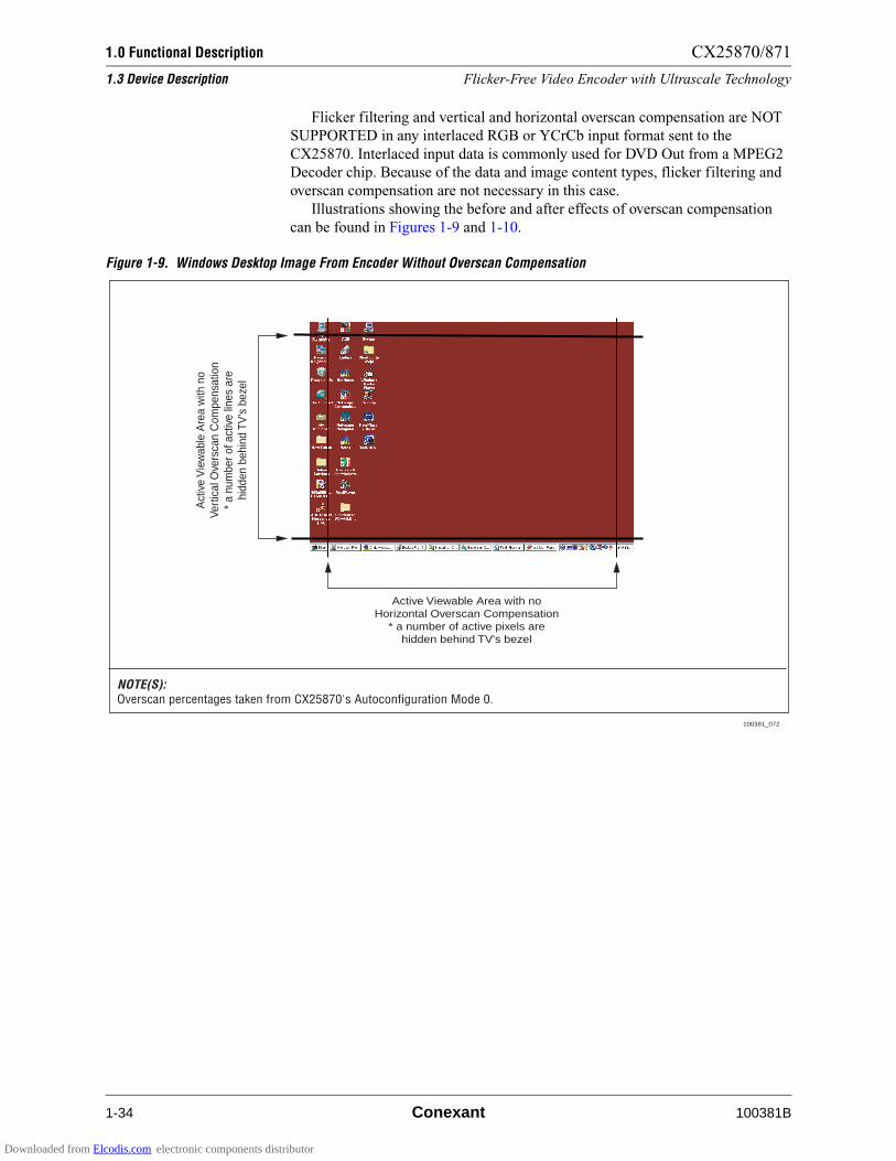
1.0 Functional Description CX25870/871
1.3 Device Description Flicker-Free Video Encoder with Ultrascale Technology
1-34 Conexant 100381B
Flicker filtering and vertical and horizontal overscan compensation are NOT
SUPPORTED in any interlaced RGB or YCrCb input format sent to the
CX25870. Interlaced input data is commonly used for DVD Out from a MPEG2
Decoder chip. Because of the data and image content types, flicker filtering and
overscan compensation are not necessary in this case.
Illustrations showing the before and after effects of overscan compensation
can be found in Figures 1-9 and 1-10.
Figure 1-9. Windows Desktop Image From Encoder Without Overscan Compensation
100381_072
Active Viewable Area with noHorizontal Overscan Compensation
* a number of active pixels arehidden behind TV's bezel
Act
ive
Vie
wab
le A
rea
with
no
Vert
ical
Ove
rsca
n C
ompe
nsat
ion
* a
num
ber o
f act
ive
lines
are
hidd
en b
ehin
d TV
's b
ezel
NOTE(S):Overscan percentages taken from CX25870's Autoconfiguration Mode 0.
Downloaded from Elcodis.com electronic components distributor

CX25870/871 1.0 Functional Description
Flicker-Free Video Encoder with Ultrascale Technology 1.3 Device Description
100381B Conexant 1-35
In Figure 1-10, the CX25870 overscan compensated the 640 horizontal active
pixels of data to fit within the viewable video region. With 13.78 percent HOC,
the active data is contained within a 45.397 !s. portion of time within each active
line while the remaining 7.26 !s (52.65556 !s.–45.397 !s.) part of the active
region is blanked by the encoder.
The net result of overscan compensation will be an interlaced NTSC, PAL, or
SECAM video image that fits within the bezel area of a TV Monitor. Correct
choice of the HOC and Vertical Overscan Compensation (VOC) percentages is
important so that no regions of the active input image will be hidden behind the
plastic of the TV unit. Various TVs require different HOC and VOC values to
fully utilize the entire viewable area of the TV. For the user’s convenience,
Conexant has generated Appendix A in the CX25870/871 datasheet which lists
many of the possible overscan ratios for the 3 major desktop resolutions
(640x480, 800x600, and 1024x768) and the 2 most popular video outputs (NTSC
and PAL-BDGHI). Varying amounts of blanking would be required depending on
the HOC and VOC percentages and active input resolutions.
Ultimately, the blanked regions would be dictated by the BLANK* signal
itself and/or the internal pixel counter for the CX25870/871. Actual transmission
of null or blanked pixels is not necessary since the encoder ignores any data sent
to it via the pixel input port within the blanked regions. Only the active pixels
need to be sent to the encoder from the controller during the digital active period.
Figure 1-10. Windows Desktop Image From CX25870 With Overscan Compensation
100381_073
13.78 % / 2 =6.89 % Blanking on Each Side
of TV
13.5
8 %
/ 2
=6.
79 %
Bla
nkin
g on
Eac
h S
ide
of T
V
NOTE(S):Overscan percentages taken from CX25870's Autoconfiguration Mode 0.
Downloaded from Elcodis.com electronic components distributor
1.0 Functional Description CX25870/871
1.3 Device Description Flicker-Free Video Encoder with Ultrascale Technology
1-36 Conexant 100381B
Figures A-1 through A-8 illustrate many of the allowable overscan
compensation percentage pairs for the major desktop resolutions and the most
popular video outputs. These figures illustrate the minimum horizontal blanking
times the data master must possess along with overscan compensation plots for
pixel based data masters as well as 8-and 9-cycle character clock based graphics
controllers.
1.3.18 Standard Flicker Filtering
To understand what flicker filtering is, one must understand two of the primary
differences between the analog video standards used by TVs and the technology
used in today’s computer monitors.
First of all, computer monitors receive their video signal in a more basic,
pristine form than TVs do. As discussed earlier, the video signal sent by a
computer to its monitor is broken into multiple electrical components (red, green,
blue and sync) while a TV signal has all necessary information combined into a
single composite signal or separate Luma and Chroma analog channels
(S-Video). In order to process this composite signal, a TV must break it up into its
original components, inevitably degrading the picture quality and creating
distortions.
A second factor contributing to the decreased quality of images displayed on
TV monitors is interlacing, a technique by which a complete TV picture is drawn
in two passes from top to bottom on the picture tube. In interlacing, the first pass
paints all the “odd” lines and the second pass paints the “even” lines. Noticeable
flicker occurs when the images in the odd lines are very different from the images
in the even lines. As the odd and even lines are alternately displayed, the eye
perceives the quick appearing and disappearing of visual information. This results
the in the irritation called flicker. Flicker is especially noticeable when viewing
thin horizontal lines that only take up a single row within the odd or even field. If,
for example, the line happens to be on an odd row, it totally disappears every time
the even rows are displayed resulting in that item appearing and disappearing at
the field rate on the TV.
Unlike TV monitors, computer monitors paint an entire image in one pass
from top to bottom, in a display format called noninterlaced or progressive.
Images displayed in a noninterlaced format do not suffer from the same flicker
problems.
For improved image quality and reduced flickering, the CX25870 contains a
5-tap or 5-line flicker filter for both the Luma (F_SELY[2:0]) channel and
Chroma (F_SELC[2:0]) channel. The Conexant standard flicker-filter works by
applying a mathematically weighted averaging algorithm to the incoming pixels
of data from different lines. This slightly alters the digital information that is
processed and eventually converted to the odd and even lines of a TV picture so
that the alternating lines are more similar to each other. This way, when they
appear and disappear in the interlacing process, the flicker is less noticeable. The
more similar the lines are made to appear, the less flicker is visible.
Downloaded from Elcodis.com electronic components distributor
CX25870/871 1.0 Functional Description
Flicker-Free Video Encoder with Ultrascale Technology 1.3 Device Description
100381B Conexant 1-37
However, the trade-off is that as flicker is reduced, more and more information
is being altered by the encoder and potentially lost from the original picture.
Vertical resolution is therefore sacrificed and text clarity suffers especially for
small fonts below 10 points in size. For this reason, the amount of flicker filtering
is programmable and should be controllable by the end user. Finding an optimal
standard flicker filter setting for Luma and Chroma is somewhat subjective in
nature and ensures that a pleasing image is seen on the television.
Unlike other encoders, the CX25870 integrates both a standard flicker filter
and additional adaptive flicker filter. This implementation allows for the
preservation of small font text clarity and other challenging video images lost
with only one filtering step. The adaptive feature eliminates more flicker with less
loss of resolution because it is able to selectively apply more aggressive flicker
reduction only to those portions of an image where the effect will be beneficial.
Encoders lacking this adaptive filter apply the standard flicker filtering process to
the entire screen. Small text and icons often become unreadable and thin,
horizontal lines may completely disappear. The CX25870’s adaptive flicker filter
prevents this from happening and is described in its own section within this
document.
So long as progressive RGB or YCrCb data is received, the CX25870’s flicker
filter is effective with any active resolution from 320x200 to a maximum of 1024
x 768. The flicker reduction is present on any interlaced video output such as
NTSC, PAL, or SECAM. The DIS_FFILT register bit turns off the standard
flicker filter. The vertical scaling can be disabled by setting the internal
V_SCALE register to 4096 for a noninterlaced input. Finally, the CX25870
supports up to 24-bit color processing, meaning that the converted image will
feature the same depth of color as the original computer picture.
1.3.19 Adaptive Flicker Filter
Adaptive Flicker Filtering is a new feature included with the CX25870/871. It
allows the encoder to automatically alter the amount of flicker filtering based on
the image being processed. The result is a high-quality optimized image because
the perfect balance between vertical resolution and flicker reduction has been
achieved. The adaptive flicker filter is enabled via the ADPT_FF bit. There are
four possible settings ranging from 2-line (most observable flicker, greatest
vertical resolution) to 5-line (minimal observable flicker, moderate vertical
resolution). The luminance and chrominance outputs are independent in terms of
the level of adaptive flicker filtering. When the adaptive flicker filter is on, the
manual flicker filter is off and vice versa.
Vertical filtering in the CX25870/871 serves three purposes:
• Vertical polyphase interpolation filtering to upsample the image data
vertically. This increases the resolution and accuracy of the subsequent
vertical downsampling required to fit the entire image into the visible
region of the television.
• Anti-alias filtering to reduce aliasing artifacts when downsampling
vertically.
• Flicker filtering to reduce the flicker produced when vertical high
frequency content is displayed on an interlaced device.
Downloaded from Elcodis.com electronic components distributor

1.0 Functional Description CX25870/871
1.3 Device Description Flicker-Free Video Encoder with Ultrascale Technology
1-38 Conexant 100381B
The vertical interpolation filtering and vertical anti-alias filtering
requirements are driven by the amount of vertical down scaling required, and do
not vary substantially with image content. The flicker filtering requirement,
however, is dependent upon the image content.
Regions of the image with vertical high frequency content will flicker in
proportion to the amplitude of that high frequency content. Regions with high
amplitude vertical high frequency content require substantial flicker filtering, but
regions with low amplitude or no vertical high frequency content require little or
no flicker filtering.
For this reason, the CX25870/871 provides adaptive flicker filtering. It
analyzes the image content to detect areas that require strong flicker filtering, and
adjusts its vertical filtering to apply stronger flicker filtering to those regions.
This analysis and adjustment occurs on a pixel by pixel basis, so each pixel in the
output line has the optimal amount of flicker filtering applied to it.
The Adaptive_FF1 and Adaptive_FF2 registers (0x34 and 0x36) configure the
adaptive algorithm. The Y_ALTFF[1:0] and C_ALTFF[1:0] fields allow the
selection of the alternative (i.e., stronger) flicker filter to combine with the
standard flicker filter selected by fields F_SELY[1:0] and F_SELC[1:0] (register
0xC8). This creates an array of flicker filters for the Y channel and C channel
respectively. The actual flicker filter applied for a given pixel output depends on
the detection and location of any high amplitude vertical high frequency content
within the input samples that creates that output pixel.
The amplitude of the high frequency content that triggers an adaptation of the
flicker filter can be adjusted via the Y_THRESH[2:0] and C_THRESH[2:0] bit
fields. The FFRTN bit offers two ways to combine the standard and alternate
flicker filters to generate an array of flicker filters. The YSELECT bit allows the
Chroma channel flicker filter to be adapted based on the Chroma channel or the Y
(i.e., Luminance) channel content.
NOTE: Neither standard nor adaptive flicker filtering is supported by the
CX25870/871 in noninterlaced video output formats (VGA style RGB,
HDTV 480p, 720p).
Table 1-16 summarizes recommended configurations of the adaptive flicker
filter for various types of image content and resolutions.
Downloaded from Elcodis.com electronic components distributor
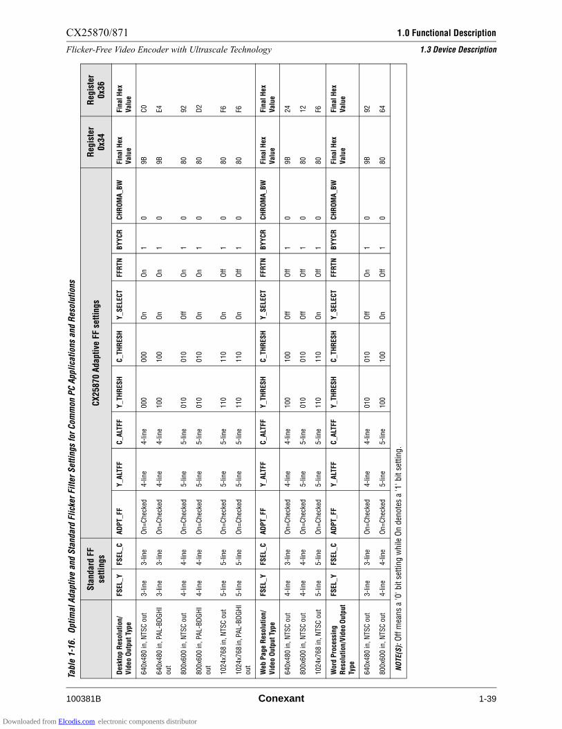
CX25870/871 1.0 Functional Description
Flicker-Free Video Encoder with Ultrascale Technology 1.3 Device Description
100381B Conexant 1-39
Tab
le 1
-16
. O
pti
ma
l A
da
pti
ve a
nd
Sta
nd
ard
Fli
cke
r F
ilte
r S
ett
ing
s fo
r C
om
mo
n P
C A
pp
lica
tio
ns
an
d R
eso
luti
on
s
Sta
nd
ard
FF
se
ttin
gs
CX
25
87
0 A
da
pti
ve F
F s
ett
ing
sR
eg
iste
r 0
x34
Reg
iste
r 0
x36
Desk
top
Reso
luti
on
/
Vid
eo O
utp
ut
Typ
e
FS
EL_
YF
SEL
_C
AD
PT_
FF
Y_A
LTF
FC
_A
LTFF
Y_
TH
RES
HC
_T
HR
ES
HY
_S
ELE
CT
FF
RT
NB
YY
CR
CH
RO
MA
_B
WF
ina
l H
ex
Valu
e
Fin
al
He
x
Va
lue
640
x48
0 in
, N
TS
C o
ut
3-l
ine
3-l
ine
On
=C
hec
ked
4-l
ine
4-l
ine
00
00
00
On
On
10
9B
C0
640
x48
0 in
, P
AL-B
DG
HI
out
3-l
ine
3-l
ine
On
=C
hec
ked
4-l
ine
4-l
ine
10
01
00
On
On
10
9B
E4
800
x60
0 in
, N
TS
C o
ut
4-l
ine
4-l
ine
On
=C
hec
ked
5-l
ine
5-l
ine
01
00
10
Off
On
10
80
92
800
x60
0 in
, P
AL-B
DG
HI
out
4-l
ine
4-l
ine
On
=C
hec
ked
5-l
ine
5-l
ine
01
00
10
On
On
10
80
D2
102
4x7
68
in, N
TS
C o
ut
5-l
ine
5-l
ine
On
=C
hec
ked
5-l
ine
5-l
ine
11
01
10
On
Off
10
80
F6
102
4x7
68
in, P
AL
-BD
GH
I
out
5-l
ine
5-l
ine
On
=C
hec
ked
5-l
ine
5-l
ine
11
01
10
On
Off
10
80
F6
We
b P
age R
eso
luti
on
/
Vid
eo O
utp
ut
Typ
e
FS
EL_
YF
SEL
_C
AD
PT_
FF
Y_A
LTF
FC
_A
LTFF
Y_
TH
RES
HC
_T
HR
ES
HY
_S
ELE
CT
FF
RT
NB
YY
CR
CH
RO
MA
_B
WF
ina
l H
ex
Valu
e
Fin
al
He
x
Va
lue
640
x48
0 in
, N
TS
C o
ut
4-l
ine
3-l
ine
On
=C
hec
ked
4-l
ine
4-l
ine
10
01
00
Off
Off
10
9B
24
800
x60
0 in
, N
TS
C o
ut
4-l
ine
4-l
ine
On
=C
hec
ked
5-l
ine
5-l
ine
01
00
10
Off
Off
10
80
12
102
4x7
68
in, N
TS
C o
ut
5-l
ine
5-l
ine
On
=C
hec
ked
5-l
ine
5-l
ine
11
01
10
On
Off
10
80
F6
Wo
rd P
roce
ssin
g
Re
solu
tio
n/V
ideo
Ou
tpu
t
Type
FS
EL_
YF
SEL
_C
AD
PT_
FF
Y_A
LTF
FC
_A
LTFF
Y_
TH
RES
HC
_T
HR
ES
HY
_S
ELE
CT
FF
RT
NB
YY
CR
CH
RO
MA
_B
WF
ina
l H
ex
Valu
e
Fin
al
He
x
Va
lue
640
x48
0 in
, N
TS
C o
ut
3-l
ine
3-l
ine
On
=C
hec
ked
4-l
ine
4-l
ine
01
00
10
Off
On
10
9B
92
800
x60
0 in
, N
TS
C o
ut
4-l
ine
4-l
ine
On
=C
hec
ked
5-l
ine
5-l
ine
10
01
00
On
Off
10
80
64
NO
TE
(S):
Off
mea
ns
a '0
' b
it s
ettin
g w
hile
On d
enote
s a
'1' bit s
etting.
Downloaded from Elcodis.com electronic components distributor

1.0 Functional Description CX25870/871
1.3 Device Description Flicker-Free Video Encoder with Ultrascale Technology
1-40 Conexant 100381B
1.3.20 VGA Registers Involved in the TV Out Process
Timing constraints for the CX25870/871 are driven by the timing requirements of
the analog video output (NTSC, PAL, or SECAM) together with the active
resolution and overscan compensation ratio (i.e., amount of blanking in the active
region) of the television image. To explain what specific CRTC or VGA registers
within the graphics controller need to be involved in displaying a nonstandard or
desktop format on both a TV and CRT, one can work backwards from those
output signal timing requirements to determine the input timing requirements.
Each output field has a vertical blanking region and an active region. These
regions are defined relative to the vertical sync pulse, horizontal sync pulse, given
format (i.e., number of lines per field), and a given pixel clock frequency (i.e.,
number of pixel clocks per line). Within each line of the active region there is a
horizontal blanking period (that includes a horizontal sync pulse) and an active
period (where the image data is located). Given those parameters, at least six
registers within every generic graphics controller need to be changed for each
active/total resolution.
Table 1-17 lists VGA/CRTC Registers Involved in TV Out Process.
To achieve VGA compatibility, the controller must manipulate some of its own
VGA register settings in order to produce a hi-quality dual display on both the
computer monitor and TV. It should be noted that the encoder has no way of
knowing that a different VGA mode has been selected. As a result, it relies on the
I2C®-compatible master device to reconfigure it via an autoconfiguration mode
or complete register rewrite to make adjustments in its timing.
When the two devices are programmed correctly, regardless of the interface,
the required input HSYNC*/VSYNC* to first input active pixel or line spacing
“matches” the output HSYNC*/VSYNC* to first output active pixel or line
spacing. When this occurs, the graphics controller always transmits active data at
the time the CX25870/871 expects to receive it. Superior TV Out quality is
achieved only when this type of timing symmetry exists.
Table 1-17. VGA/CRTC Registers Involved in TV Out Process
Register Name Description
Start VBLANK/VSYNC* andEnd VBLANK/VSYNC*
These VGA registers work in combination with each other to control the scan line at which the vertical blanking period begins and the point at which it ends.
VACTIVE Dictates the specific number of active lines for the present digital frame.
VTOTAL Specifies the number of scan lines from one VSYNC* active to the next VSYNC* active pulse.
The difference between Vtotal and Vactive is the amount of blanked lines.
HBLANK/HSYNC* Start and
HBLANK/HSYNC* End
This VGA register set works in combination with each other to control the value of the pixel or character clock counter where the HSYNC* signal becomes active and the position at which HSYNC* becomes inactive.
HACTIVE Dictates the specific number of active pixels per line.
HTOTAL Specifies the number of pixel clocks or character clocks from one HSYNC* active to the next
HSYNC* active pulse. In other words, this is the total time required for both the displayed and nondisplayed portions of a single scan line. The difference between Htotal and Hactive is the amount of blanked pixels per line.
Downloaded from Elcodis.com electronic components distributor
CX25870/871 1.0 Functional Description
Flicker-Free Video Encoder with Ultrascale Technology 1.3 Device Description
100381B Conexant 1-41
1.3.21 Output Modes
The encoder can generate output video as Composite/Y-C(S-Video), YUV
component, VGA-style RGB, SCART, Component (YPRPB) for HDTV, or RGB
for HDTV. These outputs are selected by the OUT_MODE[1:0] register bits in
combination with the HDTV_EN and EN_SCART bits.
While the encoder is in VGA style RGB, no color space conversion is possible
from input to output. Analog RGB is transmitted from a digital RGB input and
analog YCrCb is output from a digital YCrCb input.
When outputting RGB with HDTV_EN = 0, the device outputs VGA/SVGA
analog RGB with a bilevel sync. In this mode, the R, G, and B input data is fed to
the DACs after the addition of the horizontal sync and, if the SETUP bit is one,
the setup pedestal is added. The output currents are scaled so that the DACs
output the proper 1 V full-scale (sync tip to peak white) levels for driving a CRT
monitor. The graphics controller must provide all the timing control (HSYNC and
VSYNC signals) for the monitor, which results in the encoder operating as a slave
in this case. Only the P[23:0], BLANK*, HSYNC*, and VSYNC* input pins and
the RGB analog output pins are active. The BLANK*, HSYNC*, and VSYNC*
pins are automatically enabled as inputs in this mode.
Each of the four video signals generated by the OUT_MODE[1:0] field can be
multiplexed to any DAC using the OUT_MUXA[1:0], OUT_MUXB[1:0],
OUT_MUXC[1:0], and OUT_MUXD[1:0] register bits. To do this, program the
2-bit value representing the desired type of output into the appropriate
OUT_MUXx[1:0] register. As an example, suppose a system requires composite
video (i.e., 00) to be output from DAC_A, chroma (10) on DAC_B, luma (01) on
DAC_C, and composite video (00) on DAC_D. This scheme could be
accomplished by programming register 0xC6 with 0001 1000 binary or 18 hex.
The LUMADLY[1:0] register bits control the amount of delay for the Y_DLY
analog output. The allowable delay ranges from 0 (no delay) to 3 pixel clocks.
All digital-to-analog converters are designed to drive standard video levels
into a combined RLOAD of 37.5 " (doubly-terminated 75 " loads). Unused
outputs should be disabled by setting the corresponding DACDISx bit to
minimize the supply current or left as a no connect. Disabling unused DAC
outputs reduces cross chroma distortion and improves picture quality.
1.3.22 Analog Horizontal Sync
The HSYNC_WIDTH[7:0] register determines the duration of the horizontal
sync pulse. The beginning of the horizontal sync pulse corresponds to the reset of
the internal horizontal pixel counter. The horizontal line rate is determined by
H_CLKO[11:0]. The internal horizontal counter is reset to 1 at the beginning of
the horizontal sync and counts up to H_CLKO.
The sync rise and fall times are automatically controlled. The sync amplitude
is programmable over a range of values by SYNC_AMP[7:0]. Incrementing the
sync amp by 1 increases the sync amplitude of the analog sync pulse by 30
millivolts.
Downloaded from Elcodis.com electronic components distributor
1.0 Functional Description CX25870/871
1.3 Device Description Flicker-Free Video Encoder with Ultrascale Technology
1-42 Conexant 100381B
1.3.23 Analog Vertical Sync
The analog vertical sync duration is selectable as either 2.5 or 3 lines by register
bit VSYNC_DUR. If VSYNC_DUR = 1, 3 lines are selected; if
VSYNC_DUR = 0, 2.5 lines are selected.
The device automatically blanks the video from the start of the horizontal sync
interval through the end of the burst, as well as the vertical sync to prevent
erroneous video timing generation.
1.3.24 Analog Video Blanking
Analog video blanking is controlled by the H_BLANKO, V_BLANKO, and
V_ACTIVEO registers. Together they define an active region where pixels are
displayed. V_BLANKO defines the number of lines from the leading edge of the
analog vertical sync to the first active output line per field. V_ACTIVEO defines
the number of active output lines. H_BLANKO defines the number of output
pixels from the leading edge of horizontal sync to the first active output pixel.
H_ACTIVE defines the number of active output pixels.
The device automatically blanks video from the start of the horizontal sync
interval through the end of the burst, as well as the vertical sync interval to
prevent erroneous video timing generation.
1.3.25 Video Output Standards Supported
There are several bits (625LINE, SETUP, VSYNC_DUR, PAL_MD, FM,
DIS_SCRST), a PAL pin, and various autoconfiguration modes, that control the
generation of various video standards. (These are summarized in Table 1-18.)
They allow the generation of all the different NTSC, PAL, and SECAM video
standards. The aforementioned bits control the specific encoding process
parameters. It is likely other registers may need to be modified to meet all the
video parameters of the particular video standard. Video timing diagrams are
illustrated in Figures 1-11 through 1-22. These show typical events that occur for
each type of video format.
Downloaded from Elcodis.com electronic components distributor
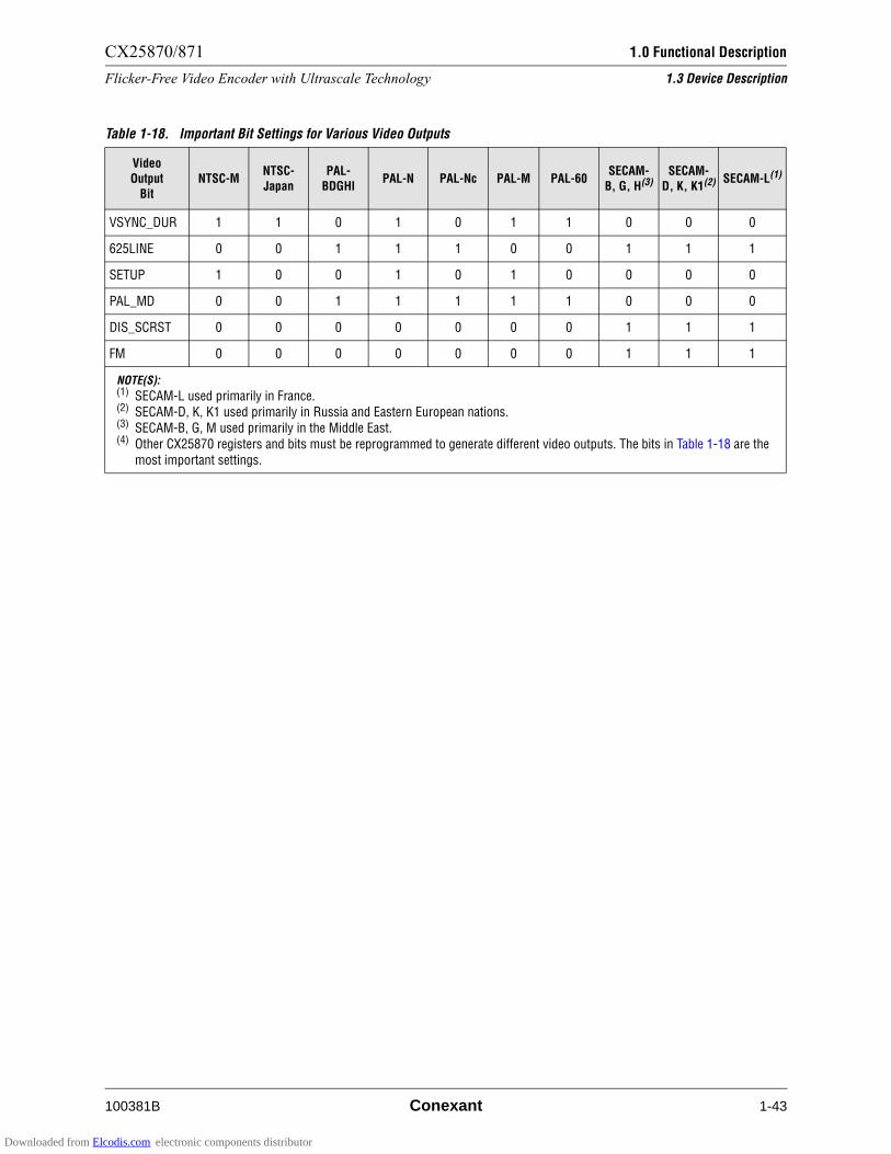
CX25870/871 1.0 Functional Description
Flicker-Free Video Encoder with Ultrascale Technology 1.3 Device Description
100381B Conexant 1-43
Table 1-18. Important Bit Settings for Various Video Outputs
Video
Output
Bit
NTSC-MNTSC-
Japan
PAL-
BDGHIPAL-N PAL-Nc PAL-M PAL-60
SECAM-
B, G, H(3)SECAM-
D, K, K1(2) SECAM-L(1)
VSYNC_DUR 1 1 0 1 0 1 1 0 0 0
625LINE 0 0 1 1 1 0 0 1 1 1
SETUP 1 0 0 1 0 1 0 0 0 0
PAL_MD 0 0 1 1 1 1 1 0 0 0
DIS_SCRST 0 0 0 0 0 0 0 1 1 1
FM 0 0 0 0 0 0 0 1 1 1
NOTE(S):(1) SECAM-L used primarily in France.(2) SECAM-D, K, K1 used primarily in Russia and Eastern European nations.(3) SECAM-B, G, M used primarily in the Middle East.(4) Other CX25870 registers and bits must be reprogrammed to generate different video outputs. The bits in Table 1-18 are the
most important settings.
Downloaded from Elcodis.com electronic components distributor
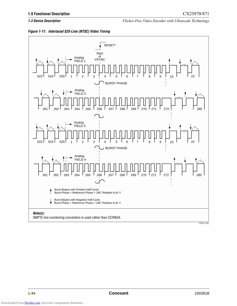
1.0 Functional Description CX25870/871
1.3 Device Description Flicker-Free Video Encoder with Ultrascale Technology
1-44 Conexant 100381B
Figure 1-11. Interlaced 525-Line (NTSC) Video Timing
Note(s):SMPTE line numbering convention is used rather than CCIR624.
2276543
BURST PHASE
21525524523
AnalogFIELD 1
Startof
VSYNC
AnalogFIELD 2
272271270269268267263262261 266265264 285
AnalogFIELD 3
BURST PHASE
AnalogFIELD 4
Burst Begins with Positive Half-CycleBurst Phase = Reference Phase = 180˚ Relative to B–Y
Burst Begins with Negative Half-CycleBurst Phase = Reference Phase = 180˚ Relative to B–Y
8 9 10
227654321525524523 8 9 10
272271270269268267263262261 266265264 285
RESET*
100381_006
Downloaded from Elcodis.com electronic components distributor

CX25870/871 1.0 Functional Description
Flicker-Free Video Encoder with Ultrascale Technology 1.3 Device Description
100381B Conexant 1-45
Figure 1-12. Interlaced 525-Line (PAL-M) Video Timing
2276543
Burst Phase
21525524523
AnalogFIELD 1
Startof
VSYNC*
AnalogFIELD 2
272271270269268267263262261 266265264
AnalogFIELD 3
Burst Phase
AnalogFIELD 4
8 9 10
7654321525524523 8 9
272271270269268267263262261 266265264
Burst Phase = Reference Phase = 135˚ Relative to UPAL Switch = 0, +V Component
Burst Phase = Reference Phase + 90˚ = 225˚ Relative to UPAL Switch = 1, –V Component
11 12
2211 12
285274273
285274273
10
RESET*
100381_007
Downloaded from Elcodis.com electronic components distributor

1.0 Functional Description CX25870/871
1.3 Device Description Flicker-Free Video Encoder with Ultrascale Technology
1-46 Conexant 100381B
Figure 1-13. Interlaced 625-Line (PAL-B, D, G, H, I, Nc) Video Timing (Fields 1–4)
2476543
– U PHASE
21622621620
AnalogFIELD 1
Startof
VSYNC
625624623 23
AnalogFIELD 2
337320318317316315314309308 312311 336319
337320317316315314308 313312311 336319
310 313
309 318310
247654321622621620 625624623 23
FIELD One
FIELD Two
FIELD Three
FIELD Four
BurstBlankingIntervals
Burst Phase = Reference Phase = 135˚ Relative to UPAL Switch = 0, +V Component
Burst Phase = Reference Phase + 90˚ = 225˚ Relative to UPAL Switch = 1, –V Component
AnalogFIELD 3
AnalogFIELD 4
RESET*
100381_008
Downloaded from Elcodis.com electronic components distributor
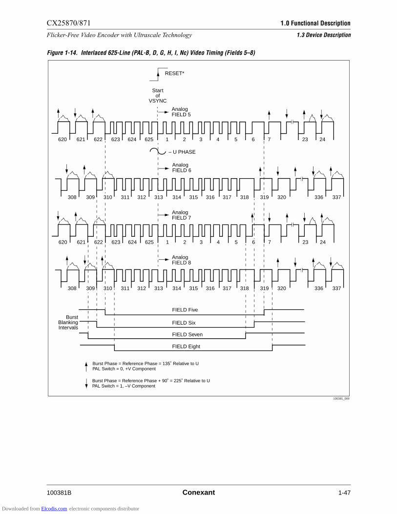
CX25870/871 1.0 Functional Description
Flicker-Free Video Encoder with Ultrascale Technology 1.3 Device Description
100381B Conexant 1-47
Figure 1-14. Interlaced 625-Line (PAL-B, D, G, H, I, Nc) Video Timing (Fields 5–8)
2476543
– U PHASE
21622621620
AnalogFIELD 5
Startof
VSYNC
625624623 23
337320318317316315314309308 312311 336319
337320317316315314308 313312311 336319
310 313
309 318310
247654321622621620 625624623 23
FIELD Five
FIELD Six
FIELD Seven
FIELD Eight
BurstBlankingIntervals
Burst Phase = Reference Phase = 135˚ Relative to UPAL Switch = 0, +V Component
Burst Phase = Reference Phase + 90˚ = 225˚ Relative to UPAL Switch = 1, –V Component
AnalogFIELD 6
AnalogFIELD 7
AnalogFIELD 8
RESET*
100381_009
Downloaded from Elcodis.com electronic components distributor
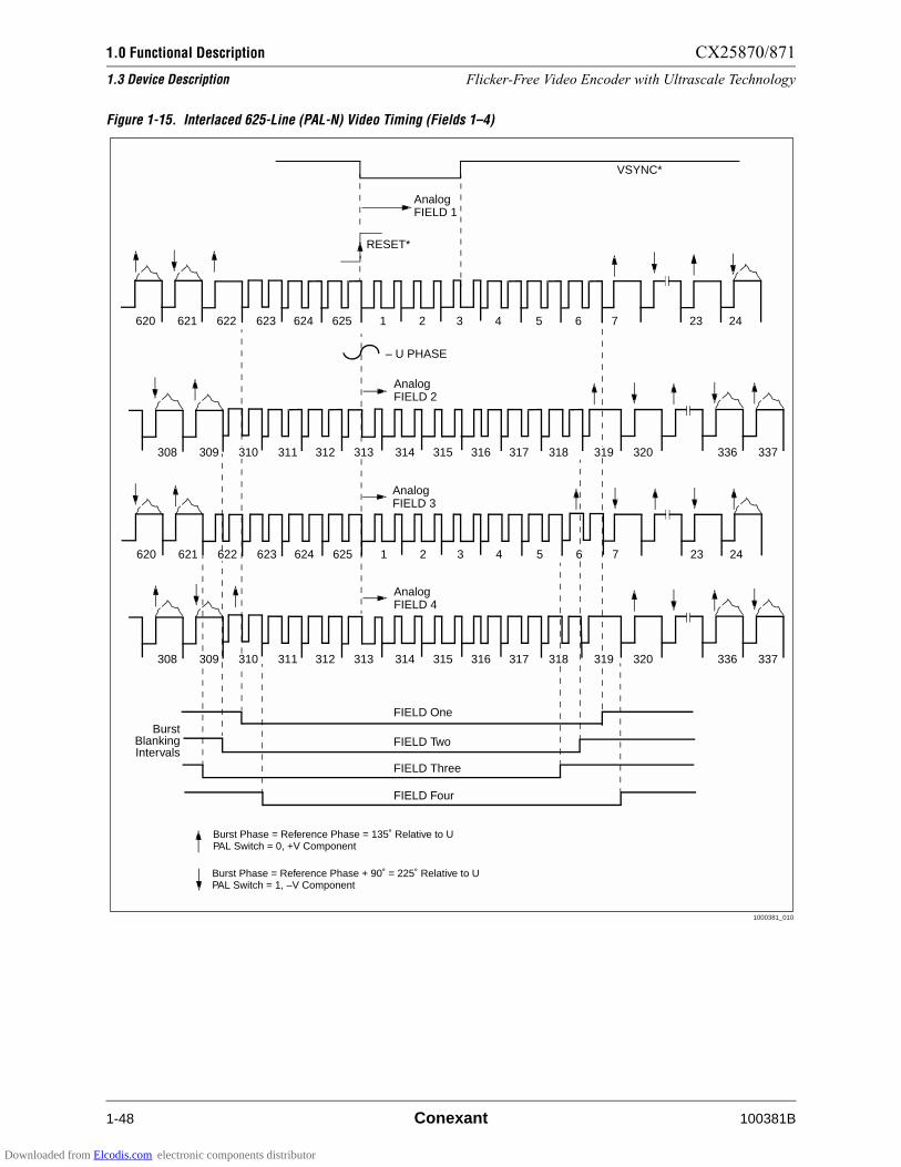
1.0 Functional Description CX25870/871
1.3 Device Description Flicker-Free Video Encoder with Ultrascale Technology
1-48 Conexant 100381B
Figure 1-15. Interlaced 625-Line (PAL-N) Video Timing (Fields 1–4)
247654321622621620 625624623 23
337320318317316315314309308 312311 336
337320317316315314308 313312311 336
24754321621620 625624623 23
– U PHASE
AnalogFIELD 1
AnalogFIELD 2
FIELD One
FIELD Two
FIELD Three
FIELD Four
BurstBlankingIntervals
Burst Phase = Reference Phase = 135˚ Relative to UPAL Switch = 0, +V Component
Burst Phase = Reference Phase + 90˚ = 225˚ Relative to UPAL Switch = 1, –V Component
AnalogFIELD 3
AnalogFIELD 4
RESET*
VSYNC*
310309
622
310 313 319
6
318 319
1000381_010
Downloaded from Elcodis.com electronic components distributor

CX25870/871 1.0 Functional Description
Flicker-Free Video Encoder with Ultrascale Technology 1.3 Device Description
100381B Conexant 1-49
Figure 1-16. Interlaced 625-Line (PAL-N) Video Timing (Fields 5–8)
2476543
– U PHASE
21622621620 625624623 23
337320318317316315314309308 312311 336319
337320317316315314308 313312311 336319
310 313
309 318310
247654321622621620 625624623 23
FIELD Five
FIELD Six
FIELD Seven
FIELD Eight
BurstBlankingIntervals
Burst Phase = Reference Phase = 135˚ Relative to UPAL Switch = 0, +V Component
Burst Phase = Reference Phase + 90˚ = 225˚ Relative to UPAL Switch = 1, –V Component
AnalogFIELD 6
AnalogFIELD 7
AnalogFIELD 8
AnalogFIELD 5
VSYNC*
100381_011
Downloaded from Elcodis.com electronic components distributor

1.0 Functional Description CX25870/871
1.3 Device Description Flicker-Free Video Encoder with Ultrascale Technology
1-50 Conexant 100381B
Figure 1-17. Noninterlaced 262-Line (NTSC) Video Timing
10 219876543
FIELD 1
21262261
STARTof
VSYNC
Burst Begins with Positive Half-CycleBurst Phase = Reference Phase = 180˚ Relative to B-Y
Burst Begins with Negative Half-CycleBurst Phase = Reference Phase = 180˚ Relative to B-Y
100381_012
Figure 1-18. Noninterlaced 262-Line (PAL-M) Video Timing
Burst Begins with Positive Half-CycleBurst Phase = Reference Phase = 180˚ Relative to B-Y
Burst Begins with Negative Half-CycleBurst Phase = Reference Phase = 180˚ Relative to B-Y
10 21987654321262261
STARTof
VSYNC
11 12
FIELD 1
100381_013
Figure 1-19. Noninterlaced 312-Line (PAL-B, D, G, H, I, N, Nc) Video Timing
237651312311310309308
Startof
VSYNC
2 3 4
RESET*
24
Burst Phase = Reference Phase = 135˚ Relative to UPAL Switch = 0, +V Component
Burst Phase = Reference Phase + 90˚ = 225˚ Relative to UPAL Switch = 1, –V Component
100381_014
Downloaded from Elcodis.com electronic components distributor

CX25870/871 1.0 Functional Description
Flicker-Free Video Encoder with Ultrascale Technology 1.3 Device Description
100381B Conexant 1-51
Figure 1-20. Interlaced 625-Line (SECAM-B, D, G, K, K1, L, M) Video Timing (Fields 1-4)
100381_091
DR
DR
DR DR
DRDB
DRDB
DRDB DBDR
DBDR
DB
DB
RESET*
End of the preceding4-field sequence
AnalogFIELD 1
AnalogFIELD 2
AnalogFIELD 3
AnalogFIELD 4
Start ofVSYNC
621
309 310 311 312 313 314 315 316 317 318 319 320 321 322 323 324 325 326 327 328 329 330 331 332 333 334 335 336
309 310 311 312 313 314 315 316 317 318 319 320 321 322 323 324 325 326 327 328 329 330 331 332 333 334 335 336
622 623 624 625 1 2 3 4 5 6 7 8 9 10 11 12 13 14 15 16 17 18 19 20 21 22 23
621 622 623 624 625 1 2 3 4 5 6 7 8 9 10 11 12 13 14 15 16 17 18 19 20 21 22 23
NOTE(S):1. DR and DB color subcarrier signal sequences over four consecutive fields shown above.2. DR color subcarrier frequency is 4.406250 MHz.3. DB color subcarrier frequency is 4.250000 MHz.
Downloaded from Elcodis.com electronic components distributor
1.0 Functional Description CX25870/871
1.3 Device Description Flicker-Free Video Encoder with Ultrascale Technology
1-52 Conexant 100381B
1.3.26 Subcarrier Generation
The device uses a 32-bit-word to synthesize the subcarrier. The value of the
subcarrier increment required to generate the desired subcarrier frequency is
found with the following equations:
NTSC:
MSC[31:0] = int((455/(2*H_CLKO)) *232 + 0.5)
PAL:
MSC[31:0] = int((1135+1/625)/H_CLKO)*232 + 0.5
SECAM:
MSC_DB[31:0] = int((272/(2*H_CLKO)*232 + 0.5)
MSC_DR[31:0] = int((272/(2*H_CLKO)*232 + 0.5)
where:H_CLKO is the number of output clocks/line (this is register 0x76 and the
low nibble of 0x86).
This allows the generation of any desired subcarrier for any desired video
standard. The 32-bit subcarrier increment must be loaded by the serial interface
before the subcarrier is enabled. The device is reset to disable chroma until the
last byte of the 32-bit increment loads, at which time the chroma is enabled,
unless the DCHROMA bit is set.
In order to prevent any residual errors from accumulating, the subcarrier DTO
(Discrete Time Oscillator) is reset every four fields for NTSC formats and every
eight fields for PAL formats. For best quality in SECAM, the DIS_SCRST bit
should be set preventing a subcarrier phase reset at the beginning of each color
field sequence. Furthermore, the SECAM subcarrier is generated on lines 23-310
and 336-623 automatically unless disabled by the PROG_SC bit.
1.3.27 Subcarrier Phase Reset/Offset
In order to maintain correct SC-H phasing, the subcarrier phase is set to 0 degrees
on the leading edge of the analog vertical sync every four (NTSC) or eight (PAL)
fields, unless the DIS_SCRST (bit four of register 0xA2) is set to a logical 1. This
is true for both interlaced and noninterlaced outputs. The subcarrier phase can be
adjusted from the nominal 0 degrees phase by the PHASE_OFF[7:0] register,
where each LSB change corresponds to a 360/256 = 1.406 degrees change in the
phase.
Setting DIS_SCRST to 1 may be useful in situations where the ratio of CLK/2
to HSYNC* edges in a color frame is noninteger, which could produce a
significant phase impulse by resetting to 0.
Downloaded from Elcodis.com electronic components distributor

CX25870/871 1.0 Functional Description
Flicker-Free Video Encoder with Ultrascale Technology 1.3 Device Description
100381B Conexant 1-53
1.3.28 Burst Generation
The subcarrier burst generation is a function of the video standard (e.g., NTSC,
PAL, or SECAM), the subcarrier frequency increment (MSC[31:0]), and the burst
horizontal begin and end register settings (HBURST_BEGIN[7:0] and
HBURST_END[7:0]). To calculate the value of HBURST_END[7:0] subtract
128 from the desired location in clock cycles. The burst will automatically be
blanked during the horizontal sync preventing invalid sync pulses from being
generated. Burst blanking is automatically controlled by the selected video
format. Burst rise and fall times are automatically generated by the device. The
burst amplitude is programmed by the BST_AMP[5:0] field.
1.3.29 Video Amplitude Scaling and SINX/X Compensation
Both the luminance and chrominance video amplitudes can be scaled by the
MCR, MCB, and MY registers. This allows various colormetry standards to be
achieved, and can also be used to boost the chroma to compensate for the sin x/x
loss of the DACs. Appendix A show the range of values achievable and values for
various video formats.
The DAC output response is a typical sinx/x response. For the composite
video output, this results in a slightly lower than desired burst and chroma
amplitude value. This is compensated for, to some extent, by choosing an output
filter that boosts the frequency response slightly. Another method which can be
used effectively, and is used by default in the auto configuration modes, is to
boost the burst and chroma gain as programmed by the BST_AMP and
MCR/MCB register values by a factor of(x/sinx). The amount of sinx/x amplitude
reduction is calculated by:
sinx/x = sin ($ * Fsc/Fclk) / ($ * Fsc/Fclk)
Fsc = desired subcarrier burst frequency
Fclk = present input clock frequency
1.3.30 Chrominance Disable
The chrominance subcarrier can be turned off by setting the DCHROMA bit to a
logical 1. This disables the subcarrier burst as well, providing luminance-only
signals on the CVBS output and a static blank level on the chrominance output.
Downloaded from Elcodis.com electronic components distributor
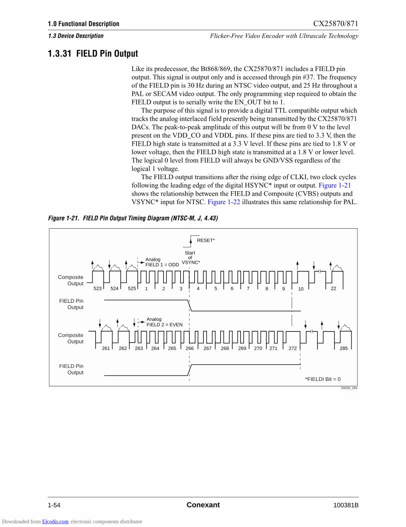
1.0 Functional Description CX25870/871
1.3 Device Description Flicker-Free Video Encoder with Ultrascale Technology
1-54 Conexant 100381B
1.3.31 FIELD Pin Output
Like its predecessor, the Bt868/869, the CX25870/871 includes a FIELD pin
output. This signal is output only and is accessed through pin #37. The frequency
of the FIELD pin is 30 Hz during an NTSC video output, and 25 Hz throughout a
PAL or SECAM video output. The only programming step required to obtain the
FIELD output is to serially write the EN_OUT bit to 1.
The purpose of this signal is to provide a digital TTL compatible output which
tracks the analog interlaced field presently being transmitted by the CX25870/871
DACs. The peak-to-peak amplitude of this output will be from 0 V to the level
present on the VDD_CO and VDDL pins. If these pins are tied to 3.3 V, then the
FIELD high state is transmitted at a 3.3 V level. If these pins are tied to 1.8 V or
lower voltage, then the FIELD high state is transmitted at a 1.8 V or lower level.
The logical 0 level from FIELD will always be GND/VSS regardless of the
logical 1 voltage.
The FIELD output transitions after the rising edge of CLKI, two clock cycles
following the leading edge of the digital HSYNC* input or output. Figure 1-21
shows the relationship between the FIELD and Composite (CVBS) outputs and
VSYNC* input for NTSC. Figure 1-22 illustrates this same relationship for PAL.
Figure 1-21. FIELD Pin Output Timing Diagram (NTSC-M, J, 4.43)
*FIELDI Bit = 0
227654321525524523
AnalogFIELD 1 = ODD
Startof
VSYNC*
AnalogFIELD 2 = EVEN
272271270269268267263262261 266265264 285
8 9 10
RESET*
100381_094
CompositeOutput
CompositeOutput
FIELD PinOutput
FIELD PinOutput
Downloaded from Elcodis.com electronic components distributor
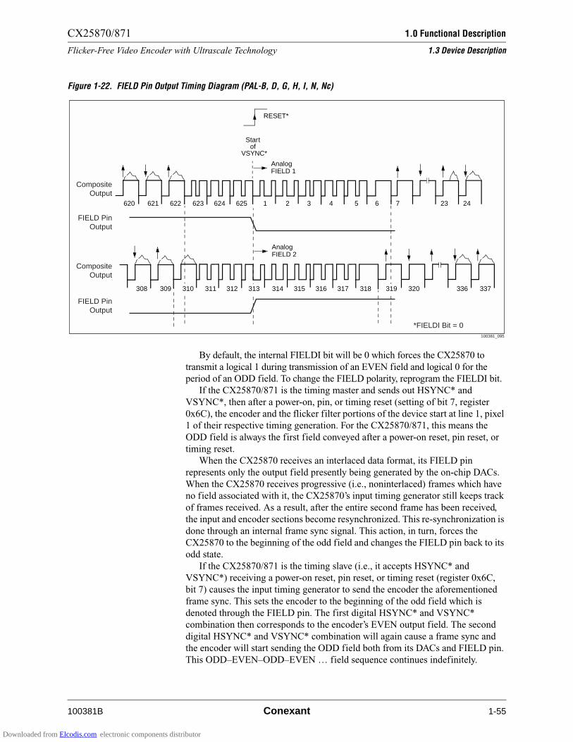
CX25870/871 1.0 Functional Description
Flicker-Free Video Encoder with Ultrascale Technology 1.3 Device Description
100381B Conexant 1-55
By default, the internal FIELDI bit will be 0 which forces the CX25870 to
transmit a logical 1 during transmission of an EVEN field and logical 0 for the
period of an ODD field. To change the FIELD polarity, reprogram the FIELDI bit.
If the CX25870/871 is the timing master and sends out HSYNC* and
VSYNC*, then after a power-on, pin, or timing reset (setting of bit 7, register
0x6C), the encoder and the flicker filter portions of the device start at line 1, pixel
1 of their respective timing generation. For the CX25870/871, this means the
ODD field is always the first field conveyed after a power-on reset, pin reset, or
timing reset.
When the CX25870 receives an interlaced data format, its FIELD pin
represents only the output field presently being generated by the on-chip DACs.
When the CX25870 receives progressive (i.e., noninterlaced) frames which have
no field associated with it, the CX25870’s input timing generator still keeps track
of frames received. As a result, after the entire second frame has been received,
the input and encoder sections become resynchronized. This re-synchronization is
done through an internal frame sync signal. This action, in turn, forces the
CX25870 to the beginning of the odd field and changes the FIELD pin back to its
odd state.
If the CX25870/871 is the timing slave (i.e., it accepts HSYNC* and
VSYNC*) receiving a power-on reset, pin reset, or timing reset (register 0x6C,
bit 7) causes the input timing generator to send the encoder the aforementioned
frame sync. This sets the encoder to the beginning of the odd field which is
denoted through the FIELD pin. The first digital HSYNC* and VSYNC*
combination then corresponds to the encoder’s EVEN output field. The second
digital HSYNC* and VSYNC* combination will again cause a frame sync and
the encoder will start sending the ODD field both from its DACs and FIELD pin.
This ODD–EVEN–ODD–EVEN … field sequence continues indefinitely.
Figure 1-22. FIELD Pin Output Timing Diagram (PAL-B, D, G, H, I, N, Nc)
247654321622621620
AnalogFIELD 1
Startof
VSYNC*
625624623 23
AnalogFIELD 2
337320318317316315314309308 312311 336319310 313
RESET*
100381_095
CompositeOutput
CompositeOutput
FIELD PinOutput
*FIELDI Bit = 0
FIELD PinOutput
Downloaded from Elcodis.com electronic components distributor

1.0 Functional Description CX25870/871
1.3 Device Description Flicker-Free Video Encoder with Ultrascale Technology
1-56 Conexant 100381B
1.3.32 Buffered Crystal Clock Output
The buffered crystal clock output (XTL_BFO) pin provides a buffered output
(0 V to 3.3 V peak-peak) of whatever frequency is found between the CX25870’s
XTALIN and XTALOUT pins. This signal can then be used as a much more
accurate input clock to the graphics controller because controllers typically utilize
clock sources with errors between 75–150 ppm. This implementation ultimately
results in better VGA picture quality because the clock driving the data master is
within the same tolerance (i.e., 25 ppm) as the TV Out encoder. This can also lead
to a considerable savings in cost, component count, and PC board space because
the crystal attached to the data master has been completely eliminated.
On power-up, the encoder will transmit a 0 to 3.3 V signal at a frequency equal
to the frequency of the crystal found between the XTALIN and XTALOUT ports.
The tolerance of the XTL_BFO signal will match the tolerance found within the
encoder’s crystal. The CX25870 was designed to expect a 13.500 MHz ± 25 ppm
crystal. As a result, all the PLL_INT and PLL_FRACT register values found
within each CX25870 autoconfiguration mode possess this set of default values.
The CX25870 does have the flexibility to support an alternate 14.31818 MHz
crystal with a tolerance of ± 25 ppm. To switch the encoder to operate with this
crystal frequency, install an appropriate crystal and crystal circuit between the
XTALIN and XTALOUT ports and set the 14318_XTAL bit to 1. Enabling this
bit translates the 13.500 MHz-dependent auto configuration registers to their new
14.31818 MHz settings.
For CX25870 designs, a small (e.g., 33 ") series resistor should be added to
XTL_BFO, as close as possible to the signal source device. This reduces
overshoot and undershoot on this signal as it changes states. The buffered crystal
clock output pin should be floated if not used. Disabling the XTL_BFO pin is
possible through the XTL_BFO_DIS bit.
1.3.33 Noninterlaced Output
When the CX25870/871 is programmed for noninterlaced video out via the
NI_OUT bit, it always transmits the odd field. The FIELD pin will continue to
change state on the leading edge of the analog vertical sync. A 30 Hz offset
should be subtracted from the color subcarrier frequency while in NTSC mode so
that the color subcarrier phase is inverted from field to field. The transition from
interlaced to noninterlaced in master interface occurs during odd fields to prevent
synchronization disturbance.
NOTE: Consumer VCRs can record noninterlaced video with minor noise
artifacts, but special effects (e.g., scan >2x) may not function properly.
Downloaded from Elcodis.com electronic components distributor
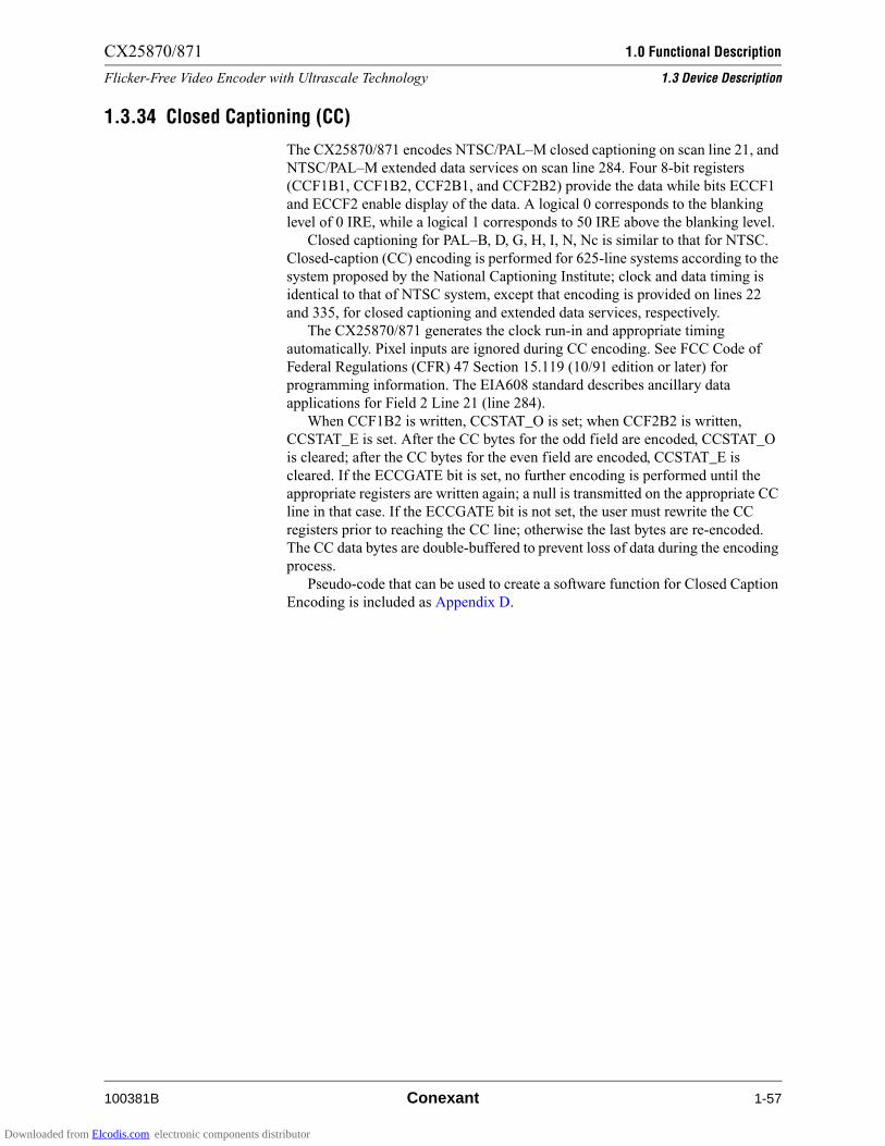
CX25870/871 1.0 Functional Description
Flicker-Free Video Encoder with Ultrascale Technology 1.3 Device Description
100381B Conexant 1-57
1.3.34 Closed Captioning (CC)
The CX25870/871 encodes NTSC/PAL–M closed captioning on scan line 21, and
NTSC/PAL–M extended data services on scan line 284. Four 8-bit registers
(CCF1B1, CCF1B2, CCF2B1, and CCF2B2) provide the data while bits ECCF1
and ECCF2 enable display of the data. A logical 0 corresponds to the blanking
level of 0 IRE, while a logical 1 corresponds to 50 IRE above the blanking level.
Closed captioning for PAL–B, D, G, H, I, N, Nc is similar to that for NTSC.
Closed-caption (CC) encoding is performed for 625-line systems according to the
system proposed by the National Captioning Institute; clock and data timing is
identical to that of NTSC system, except that encoding is provided on lines 22
and 335, for closed captioning and extended data services, respectively.
The CX25870/871 generates the clock run-in and appropriate timing
automatically. Pixel inputs are ignored during CC encoding. See FCC Code of
Federal Regulations (CFR) 47 Section 15.119 (10/91 edition or later) for
programming information. The EIA608 standard describes ancillary data
applications for Field 2 Line 21 (line 284).
When CCF1B2 is written, CCSTAT_O is set; when CCF2B2 is written,
CCSTAT_E is set. After the CC bytes for the odd field are encoded, CCSTAT_O
is cleared; after the CC bytes for the even field are encoded, CCSTAT_E is
cleared. If the ECCGATE bit is set, no further encoding is performed until the
appropriate registers are written again; a null is transmitted on the appropriate CC
line in that case. If the ECCGATE bit is not set, the user must rewrite the CC
registers prior to reaching the CC line; otherwise the last bytes are re-encoded.
The CC data bytes are double-buffered to prevent loss of data during the encoding
process.
Pseudo-code that can be used to create a software function for Closed Caption
Encoding is included as Appendix D.
Downloaded from Elcodis.com electronic components distributor
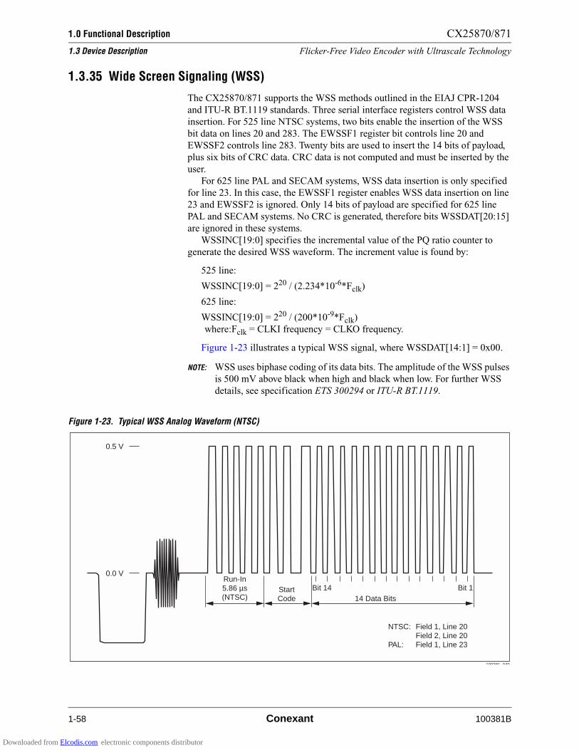
1.0 Functional Description CX25870/871
1.3 Device Description Flicker-Free Video Encoder with Ultrascale Technology
1-58 Conexant 100381B
1.3.35 Wide Screen Signaling (WSS)
The CX25870/871 supports the WSS methods outlined in the EIAJ CPR-1204
and ITU-R BT.1119 standards. Three serial interface registers control WSS data
insertion. For 525 line NTSC systems, two bits enable the insertion of the WSS
bit data on lines 20 and 283. The EWSSF1 register bit controls line 20 and
EWSSF2 controls line 283. Twenty bits are used to insert the 14 bits of payload,
plus six bits of CRC data. CRC data is not computed and must be inserted by the
user.
For 625 line PAL and SECAM systems, WSS data insertion is only specified
for line 23. In this case, the EWSSF1 register enables WSS data insertion on line
23 and EWSSF2 is ignored. Only 14 bits of payload are specified for 625 line
PAL and SECAM systems. No CRC is generated, therefore bits WSSDAT[20:15]
are ignored in these systems.
WSSINC[19:0] specifies the incremental value of the PQ ratio counter to
generate the desired WSS waveform. The increment value is found by:
525 line:
WSSINC[19:0] = 220 / (2.234*10-6*Fclk)
625 line:
WSSINC[19:0] = 220 / (200*10-9*Fclk)
where:Fclk = CLKI frequency = CLKO frequency.
Figure 1-23 illustrates a typical WSS signal, where WSSDAT[14:1] = 0x00.
NOTE: WSS uses biphase coding of its data bits. The amplitude of the WSS pulses
is 500 mV above black when high and black when low. For further WSS
details, see specification ETS 300294 or ITU-R BT.1119.
Figure 1-23. Typical WSS Analog Waveform (NTSC)
14 Data BitsStartCode
Run-In5.86 µs(NTSC)
Bit 14 Bit 1
0.5 V
0.0 V
100381 040
NTSC: Field 1, Line 20Field 2, Line 20
PAL: Field 1, Line 23
Downloaded from Elcodis.com electronic components distributor

CX25870/871 1.0 Functional Description
Flicker-Free Video Encoder with Ultrascale Technology 1.3 Device Description
100381B Conexant 1-59
The CX25870 does not support the CGMS/A standard for analog PAL or
analog NTSC video systems. CGMS stands for Copy Generation Management
System whereby scan line 23 of PAL Field 1 or lines 20 and 283 of NTSC video
outputs contains a data burst which details the signal format. The burst also
specifies the aspect ratio, type of enhanced services, and subtitle location for the
TV to use during the broadcasted show.
In addition to the details about the signal format, the CGMS bits can indicate
whether a recording device can make no copies, one copy, or unlimited copies. If
no copies are allowed, the recording device will not make a copy. If a single copy
is allowed, the recording device will make one copy and change the CGMS data
to indicate that no future copies can be made from the native content.
The major reasons the CX25870 does not support the analog method of
CGMS/A are as follows:
• No movie studio even considers the notion of allowing the user to make a
single copy. All DVDs released from the movie industry now enable the
Macrovision copy protection system so it is impossible to make any copies
of DVDs in the analog domain.
• There are no plans for DVD content providers to allow users to make
limited copies of their intellectually copyrighted material.
• Some aspects of the CGMS/A system are not pirate-proof and can be
disabled remotely.
• The CGMS/A standard appears to be a vendor rather than a DVD
consortium mandate. Only a few DVD players have this feature now, and it is
expected that they will abandon this as newer versions of the Macrovision
standard are released or a tamper-proof version of CGMS exists.
1.3.36 Chrominance and Luminance Processing
Once the input data is converted to internal YUV format, the Y and UV
components are filtered and upsampled to the system clock frequency.
The luminance signal is always low-pass filtered using the upsampling filter
response illustrated in Figure 1-24. Additional peaking or reduction filters can be
enabled (see Figures 1-25, 1-26, and 1-27), using the PKFIL_SEL[1:0] register
field. The peaking filters are optimized for high bandwidth frequency response,
and optimal picture quality.
The default chrominance filter response is illustrated in Figure 1-28, but an
alternate wide bandwidth response can be selected using register bit
CHROMA_BW, as illustrated in Figure 1-29.
Figure 1-30 illustrates the SECAM pre-emphasis filter response for the
modulated chrominance signal.
Downloaded from Elcodis.com electronic components distributor
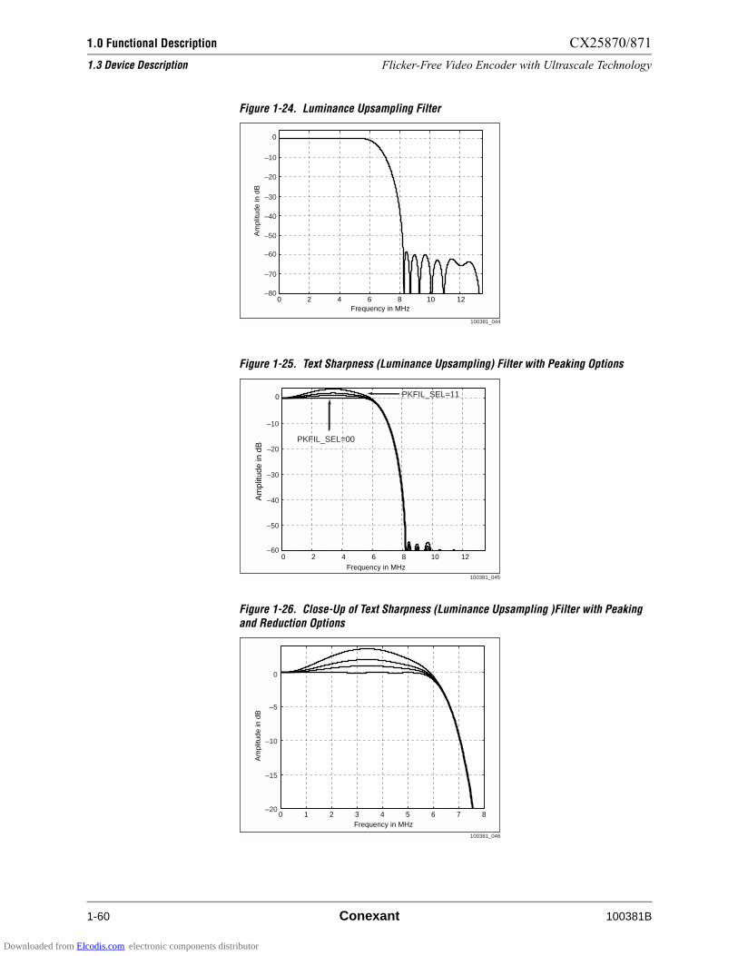
1.0 Functional Description CX25870/871
1.3 Device Description Flicker-Free Video Encoder with Ultrascale Technology
1-60 Conexant 100381B
Figure 1-24. Luminance Upsampling Filter
Figure 1-25. Text Sharpness (Luminance Upsampling) Filter with Peaking Options
Figure 1-26. Close-Up of Text Sharpness (Luminance Upsampling )Filter with Peaking and Reduction Options
0 2 4 6 8 10 12
0
Am
plitu
de in
dB
Frequency in MHz
100381_044
–10
–20
–30
–40
–50
–60
–70
–80
100381_045
0 2 4 6 8 10 12
0
Am
plitu
de in
dB
Frequency in MHz
–10
–20
–30
–40
–50
–60
PKFIL_SEL=00
PKFIL_SEL=11
100381_046
0 1 2 3 4 5 6 7 8
Am
plitu
de in
dB
Frequency in MHz
0
–5
–10
–15
–20
Downloaded from Elcodis.com electronic components distributor
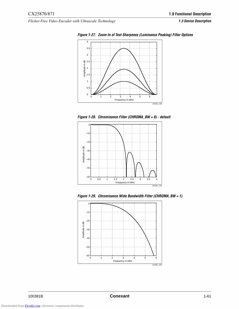
CX25870/871 1.0 Functional Description
Flicker-Free Video Encoder with Ultrascale Technology 1.3 Device Description
100381B Conexant 1-61
Figure 1-27. Zoom-In of Text Sharpness (Luminance Peaking) Filter Options
Figure 1-28. Chrominance Filter (CHROMA_BW = 0) - default
Figure 1-29. Chrominance Wide Bandwidth Filter (CHROMA_BW = 1)
0 1 2 3 4 5 60
0.5
1
1.5
2
2.5
3
3.5
4
Am
plitu
de in
dB
Frequency in MHz
100381_048
100381_049
0 0.5 1 1.5 2 2.5 3 3.5 4
0
Am
plitu
de in
dB
Frequency in MHz
–10
–20
–30
–40
–50
–60
100381_050
0 1 2 3 4 5 6Frequency in MHz
Am
plitu
de in
dB
–10
0
–20
–30
–40
–50
–60
Downloaded from Elcodis.com electronic components distributor

1.0 Functional Description CX25870/871
1.3 Device Description Flicker-Free Video Encoder with Ultrascale Technology
1-62 Conexant 100381B
1.3.37 Color Bar and Blue Field Generation
The CX25870/871 has two internal color bar generators. Preflicker filter color
bars are enabled by setting the FFCBAR bit to a logical 1. Postflicker filter color
bars are enabled by setting the ECBAR bit to a logical 1.
NOTE: FFCBAR color bars are optimized for RGB input mode and ECBAR color
bars are optimized for YCrCb input mode.
The device uses the H_BLANKO register value to determine the starting point
of the color bars, and the H_ACTIVE register value to determine the width. Eight
bars are displayed, with the colors and amplitudes being generated internally. The
pixel inputs (P23–P0) are ignored in color bar mode. The CX25870/871 must be
programmed with the appropriate MY, MCR, and MCB register values for the
desired input format, RGB or YCrCb.
The CX25870/871 also produces a blue field by setting register bit EBLUE
to 1. Pixel inputs are ignored while any of the color generation wave forms are
being produced.
Figure 1-30. SECAM High Frequency Pre-emphasis Filter
3.5 4 4.5 5
0
2
4
6
8
10
12
14
16
Frequency in MHz
Am
plitu
de in
dB
100381_051
Downloaded from Elcodis.com electronic components distributor
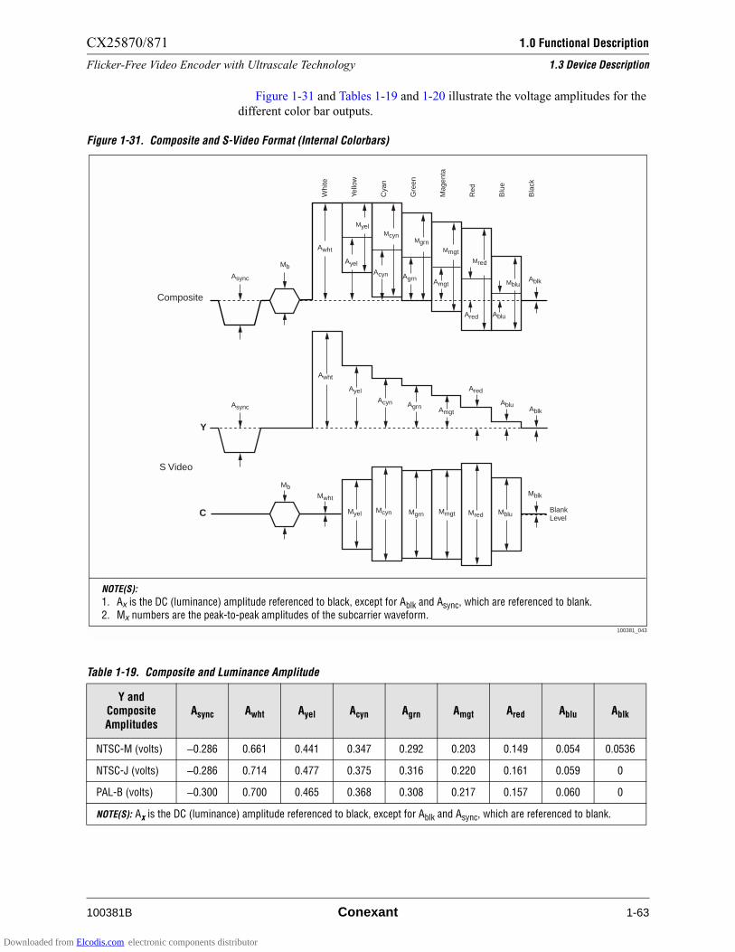
CX25870/871 1.0 Functional Description
Flicker-Free Video Encoder with Ultrascale Technology 1.3 Device Description
100381B Conexant 1-63
Figure 1-31 and Tables 1-19 and 1-20 illustrate the voltage amplitudes for the
different color bar outputs.
Figure 1-31. Composite and S-Video Format (Internal Colorbars)
Whi
te
Yello
w
Cya
n
Gre
en
Mag
enta
Red
Blu
e
Bla
ck
BlankLevel
Awht
AyelAcyn Agrn Amgt
Ared Ablu
Ablk
Ablk
MblkMwht
Async
Myel Mcyn Mgrn Mmgt Mred Mblu
Awht
Ayel
Acyn Agrn Amgt
Ared
AbluAsync
Mb
Myel
Mblu
McynMgrn
MmgtMred
Composite
S Video
Y
C
Mb
100381_043
NOTE(S):
1. A is the DC (luminance) amplitude referenced to black, except for Ablk and Async, which are referenced to blank. 2. M numbers are the peak-to-peak amplitudes of the subcarrier waveform.
x
x
Table 1-19. Composite and Luminance Amplitude
Y and Composite Amplitudes
Async Awht Ayel Acyn Agrn Amgt Ared Ablu Ablk
NTSC-M (volts) –0.286 0.661 0.441 0.347 0.292 0.203 0.149 0.054 0.0536
NTSC-J (volts) –0.286 0.714 0.477 0.375 0.316 0.220 0.161 0.059 0
PAL-B (volts) –0.300 0.700 0.465 0.368 0.308 0.217 0.157 0.060 0
NOTE(S): Ax is the DC (luminance) amplitude referenced to black, except for Ablk and Async, which are referenced to blank.
Downloaded from Elcodis.com electronic components distributor
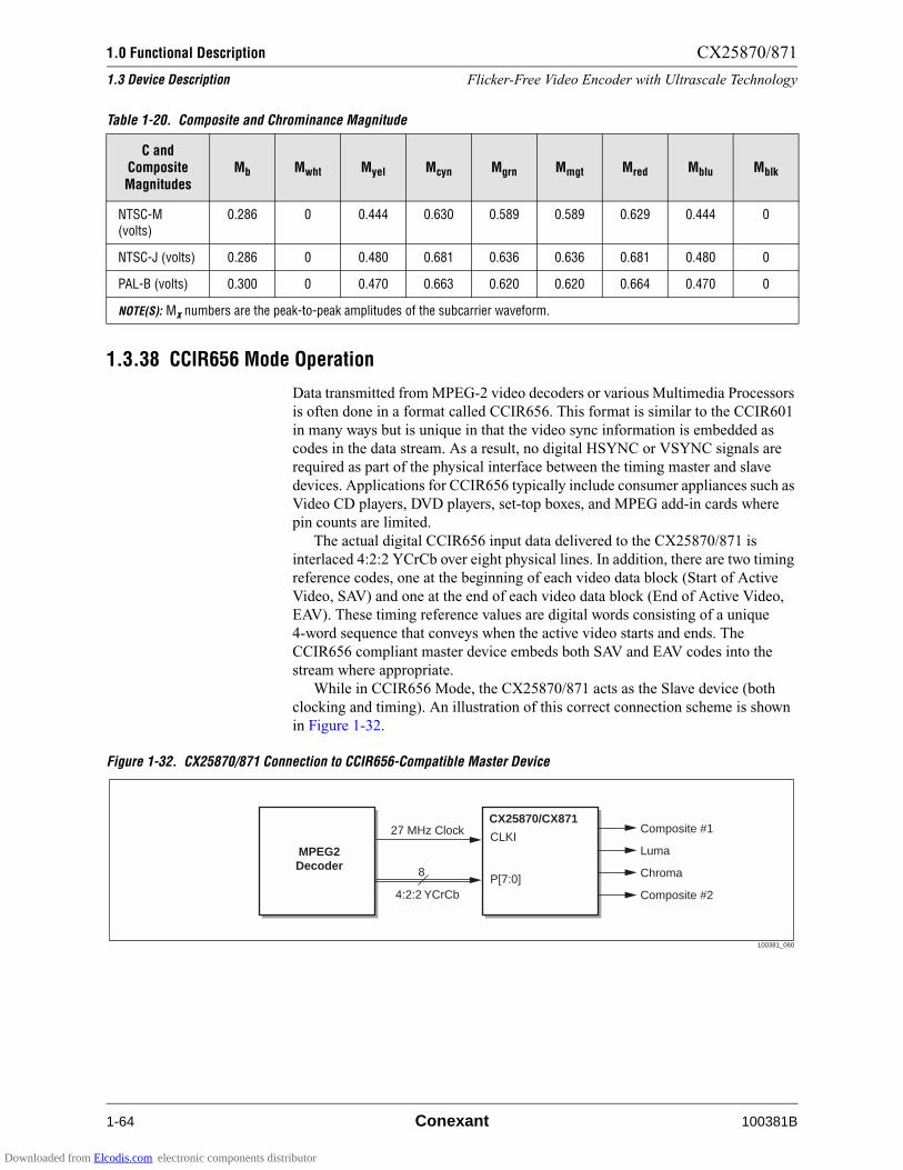
1.0 Functional Description CX25870/871
1.3 Device Description Flicker-Free Video Encoder with Ultrascale Technology
1-64 Conexant 100381B
1.3.38 CCIR656 Mode Operation
Data transmitted from MPEG-2 video decoders or various Multimedia Processors
is often done in a format called CCIR656. This format is similar to the CCIR601
in many ways but is unique in that the video sync information is embedded as
codes in the data stream. As a result, no digital HSYNC or VSYNC signals are
required as part of the physical interface between the timing master and slave
devices. Applications for CCIR656 typically include consumer appliances such as
Video CD players, DVD players, set-top boxes, and MPEG add-in cards where
pin counts are limited.
The actual digital CCIR656 input data delivered to the CX25870/871 is
interlaced 4:2:2 YCrCb over eight physical lines. In addition, there are two timing
reference codes, one at the beginning of each video data block (Start of Active
Video, SAV) and one at the end of each video data block (End of Active Video,
EAV). These timing reference values are digital words consisting of a unique
4-word sequence that conveys when the active video starts and ends. The
CCIR656 compliant master device embeds both SAV and EAV codes into the
stream where appropriate.
While in CCIR656 Mode, the CX25870/871 acts as the Slave device (both
clocking and timing). An illustration of this correct connection scheme is shown
in Figure 1-32.
Table 1-20. Composite and Chrominance Magnitude
C and Composite Magnitudes
Mb Mwht Myel Mcyn Mgrn Mmgt Mred Mblu Mblk
NTSC-M
(volts)
0.286 0 0.444 0.630 0.589 0.589 0.629 0.444 0
NTSC-J (volts) 0.286 0 0.480 0.681 0.636 0.636 0.681 0.480 0
PAL-B (volts) 0.300 0 0.470 0.663 0.620 0.620 0.664 0.470 0
NOTE(S): Mx numbers are the peak-to-peak amplitudes of the subcarrier waveform.
Figure 1-32. CX25870/871 Connection to CCIR656-Compatible Master Device
MPEG2Decoder
CLKI
P[7:0]
27 MHz Clock
8
4:2:2 YCrCb
Composite #1
Luma
Chroma
Composite #2
CX25870/CX871
100381_060
Downloaded from Elcodis.com electronic components distributor
CX25870/871 1.0 Functional Description
Flicker-Free Video Encoder with Ultrascale Technology 1.3 Device Description
100381B Conexant 1-65
While in CCIR656 Mode, the encoder adheres to all input guidelines specified
in the ITU-R BT.656-3 standard. This specification was developed for the
transmission of color video signals in YCrCb format at a pixel rate of
27.000 MHz without the use of dedicated timing reference signals.
To display a DVD movie on a TV and computer monitor simultaneously with
high-quality MPEG2 image format, the CX25870/871 must be integrated into the
hardware design. Next, actual CCIR656 data must be sent from a MPEG2
decoding master device directly to the CX25870/871 encoder. Finally, various
software steps are necessary so the encoder switches to its Slave interface and is
set up to accept the interlaced YCrCb data and video timing reference codes.
The first programming step is to configure the CX25870/871 to accept
interlaced 4:2:2 YCrCb data with an active resolution of 720x480 and output a
standard NTSC video output. The pertinent set of conditions for this option are:
Given this set of conditions, autoconfiguration mode 28 is a perfect fit. As a
result, simply use the MPEG2 decoders serial bus mastering ability to program
the CX25870/871s CONFIG[5:0] field with a binary value of 011100. This
translates into writing a hexadecimal number of 0x34 to register 0xB8. Once the
encoder acknowledges this write to its autoconfiguration register, it automatically
loads the appropriate values for this type of DVD configuration into its register
indices from 0x76 to 0xB4, including register 0x38. The exact data transferred
into these registers is contained in Appendix C.
After completion of the autoconfiguration command, the encoder expects to
receive interlaced 4:2:2 YCrCb data from the clock and timing master device at a
rate of 27.000 MHz with blanking regions being defined by HSYNC* and
VSYNC*. Since these external signals, by definition, do not exist in CCIR656
mode, a second and final programming step is required.
After enabling autoconfiguration mode 28, the programmer must make sure to
set (=1) the E656 bit. This is bit 6 of register 0xD6 and enables a CCIR656 input
to be received via the CX25870/871s P[7:0] port. Once this is done, the encoder
deciphers digital blanking through the SAV and EAV codes and disregards the
synchronization signals.
Only after the completion of these steps will a DVD stream be properly
encoded and rendered onto the television by the VGA Encoder.
For CCIR Mode operation with a PAL Composite or S-Video output, use
Autoconfiguration Mode 29 instead of autoconfiguration mode 28 and program
the master device to send a digital frame with an active resolution of 720x576.
• Type of Digital Video Input: Interlaced 4:2:2 YCrCb
• Active Resolution (HorizontalxVertical): 720 pixels x 480 lines
• Overscan Compensation: None. Horizontal = 0%; Vertical = 0%
• Interface: CX25870/871 is clock and timing slave
• Pixel Rate 27.000 MHz
• Type of Analog Video Output: Standard NTSC[NTSC-M]
Downloaded from Elcodis.com electronic components distributor

1.0 Functional Description CX25870/871
1.3 Device Description Flicker-Free Video Encoder with Ultrascale Technology
1-66 Conexant 100381B
1.3.39 CCIR601 Mode Operation for DVD Playback
Data coming from a DVD is decoded by a MPEG2 decoder or graphics controller
into a format called CCIR601. CCIR601 is the more common name for 4:2:2
YCrCb data at a 27 MHz pixel rate, as specified in the ITU-R BT.601 standard.
This specification was developed specifically for the digitalization of color video
signals.
To play a DVD movie on a television in addition to a CRT monitor, the
CX25870/871, a CCIR601 compatible encoder, must be integrated into the
hardware design. Actual CCIR601 data must be sent from a MPEG2 decoding
master device directly to the CX25870/871 encoder. This can be either a
dedicated MPEG2 decoder chip or a graphics controller with this functionality.
Various software steps are necessary so the encoder enters slave or master
interface and is set up to accept the interlaced YCrCb data or noninterlaced RGB
digital format. After all of these steps have been executed properly, a DVD movie
stream is properly encoded and rendered onto the television by the VGA encoder.
There are different capabilities among graphics controllers, MPEG2 decoders,
and proprietary ASICs that impact the particular DVD implementation. This
section seeks to cover all the possible hardware/software configurations and the
trade-offs associated with each. If the reader has an interface idea about the
routing of data from the CCIR601 source to encoder that is not discussed here,
please contact your local Conexant Field Applications Engineer for further
technical support.
1.3.39.1 CCIR601 DataIn/NTSC Out
The first option to playing a DVD movie via the CX25870/871 is to send the
digital video CCIR601 data directly to the encoder from the MPEG2 decoder. In
this case, the graphics controller does not have any effect on the CCIR601 digital
stream arriving at the input of the encoder because it bypassed the data or the data
was routed around the controller. In either case, the CX25870/871 must be
configured to accept interlaced 4:2:2 YCrCb data with an active resolution of
720x480 and output a standard NTSC video output. The pertinent set of
conditions for this option are:
Given this set of conditions, autoconfiguration mode 28 is a perfect fit for this
architectural option. As a result, simply use the MPEG2 decoders serial bus
mastering ability to program the CX25870/871s CONFIG[5:0] field with a binary
value of 011100. This translates into writing a hexadecimal number of 0x34 to
register 0xB8. Once the encoder acknowledges this write to its autoconfiguration
register, it automatically loads the appropriate value for this type of DVD
configuration into its register indices from 0x76 to 0xB4 including 0x38. The
exact data transferred into these registers is contained in Appendix C.
• Type of Digital Video Input: Interlaced 4:2:2 YCrCb
• Active Resolution (HorizontalxVertical): 720 pixels x 480 lines
• Overscan Compensation: None. Horizontal = 0%; Vertical = 0%
• Interface: CX25870/871 is clock and timing slave
• Pixel Rate 27.000 MHz
• Type of Analog Video Output: Standard NTSC[NTSC-M]
Downloaded from Elcodis.com electronic components distributor

CX25870/871 1.0 Functional Description
Flicker-Free Video Encoder with Ultrascale Technology 1.3 Device Description
100381B Conexant 1-67
After completion of the autoconfiguration command, the encoder expects to
receive interlaced CCIR601 data from the clock and timing master device at a rate
of 27.000 MHz. If this occurs, approximately 40 clocks later (i.e., pipeline delay),
the encoder begins transmitting a NTSC-compatible S-Video or Composite Video
signal containing the DVD movie.
1.3.39.2 CCIR601 DataIn/PAL Out
The second option is very similar to the first. In this scenario, the interlaced
CCIR601 video data is transmitted directly to the encoder from the MPEG2
decoder. However, instead of generating a NTSC signal, the encoder produces a
PAL-BDGHI compatible DVD movie output. The active resolution changes as
well for this alternative by increasing to 720x576.
To enable DVD playback in this scenario, the CX25870/871 must be
configured to accept interlaced 4:2:2 YCrCb data with an active resolution of
720x576 and output a standard PAL video output. The pertinent set of conditions
for this option are:
Given this set of conditions, autoconfiguration mode 29 is a perfect fit for this
architectural option. As a result, simply use the MPEG2 decoder’s serial bus
mastering ability to program the CX25870/871s CONFIG[5:0] field with a binary
value of 011101. This translates into writing a hexadecimal number of 0x35 to
register 0xB8. Once the encoder acknowledges this write to its autoconfiguration
register, it automatically loads the appropriate value for this type of DVD
configuration into its register indices from 0x76 to 0xB4 including 0x38. The
exact data transferred into these registers is contained in Appendix C.
After completion of the autoconfiguration command, the encoder expects to
receive interlaced CCIR601 data from the clock and timing master device at a rate
of 27.000 MHz. If this occurs, approximately 40 clocks later (i.e., pipeline delay),
the encoder will begin transmitting a PAL-compliant S-Video or Composite video
signal containing the DVD Movie.
1.3.39.3 VGA-Compatible RGB Data
In/NTSC Out
The third option for DVD playback is unlike the previous two methods. In this
case, the MPEG2 decoder’s 4:2:2 YCrCb interlaced data is sent as an input to the
graphics controller. In turn, the controller deinterlaces and color space converts
the CCIR601 data into a noninterlaced RGB format. The encoder finally ends up
receiving this standard VGA digital data from the graphics controllers digital
output port for generation into an analog TV signal.
• Type of Digital Video Input: Interlaced, 4:2:2 YCrCb
• Active Resolution (HorizontalxVertical): 720 pixels x 576 lines
• Overscan Compensation: None. Horizontal = 0%; Vertical = 0%
• Interface: CX25870/871 is clock and timing slave
• Pixel Rate 27.000 MHz
• Type of Analog Video Output: Standard PAL[PAL-BDGHI]
Downloaded from Elcodis.com electronic components distributor
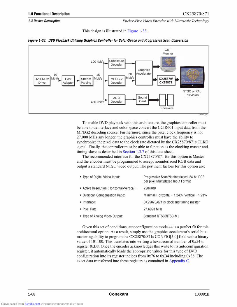
1.0 Functional Description CX25870/871
1.3 Device Description Flicker-Free Video Encoder with Ultrascale Technology
1-68 Conexant 100381B
This design is illustrated in Figure 1-33.
To enable DVD playback with this architecture, the graphics controller must
be able to deinterlace and color space convert the CCIR601 input data from the
MPEG2 decoding source. Furthermore, since the pixel clock frequency is not
27.000 MHz any longer, the graphics controller must have the ability to
synchronize the pixel data to the clock rate dictated by the CX25870/871s CLKO
signal. Finally, the controller must be able to function as the clocking master and
timing slave as described in Section 1.3.7 of this data sheet.
The recommended interface for the CX25870/871 for this option is Master
and the encoder must be programmed to accept noninterlaced RGB data and
output a standard NTSC video output. The pertinent factors for this option are:
Given this set of conditions, autoconfiguration mode 44 is a perfect fit for this
architectural option. As a result, simply use the graphics accelerator’s serial bus
mastering ability to program the CX25870/871s CONFIG[5:0] field with a binary
value of 101100. This translates into writing a hexadecimal number of 0x54 to
register 0xB8. Once the encoder acknowledges this write to its autoconfiguration
register, it automatically loads the appropriate values for this type of DVD
configuration into its register indices from 0x76 to 0xB4 including 0x38. The
exact data transferred into these registers is contained in Appendix C.
Figure 1-33. DVD Playback Utilizing Graphics Controller for Color-Space and Progressive Scan Conversion
CRTMonitor
100381_061
DVD-ROMDrive
10Mbit/s
15Mbit/s
100 kbit/s
450 kbit/s
Speakers
NTSC or PALTelevision
20Mbit/sHost
AdapterStreamParsing
GraphicsAccelerator
SoundCard
CX25870/CX25871
SubpictureDecoder
MPEG-2Decoder
AC-3Decoder
• Type of Digital Video Input: Progressive Scan/Noninterlaced; 24-bit RGB per pixel Multiplexed Input Format
• Active Resolution (HorizontalxVertical): 720x480
• Overscan Compensation Ratio: Minimal; Horizontal = 1.24%; Vertical = 1.23%
• Interface: CX25870/871 is clock and timing master
• Pixel Rate 27.6923 MHz
• Type of Analog Video Output: Standard NTSC[NTSC-M]
Downloaded from Elcodis.com electronic components distributor

CX25870/871 1.0 Functional Description
Flicker-Free Video Encoder with Ultrascale Technology 1.3 Device Description
100381B Conexant 1-69
After completion of the autoconfiguration command, the encoder enters
Master interface. In addition, the CX25870/871 will expect to receive digital
frames with an active resolution of 720x480 comprised of noninterlaced RGB
data at a pixel rate of 27.6923 MHz. If these events occur, approximately 40
clocks later (i.e., pipeline delay), the encoder will begin transmitting a
NTSC-compliant S-Video or Composite video signal containing the DVD movie.
1.3.40 SECAM Output
Unlike its predecessor, the Bt868/869, the CX25870/871 now includes an encoder
block for conversion of digital video data into a SECAM Composite (CVBS)
and/or a SECAM S-Video signal.
Like other video outputs, any active resolution from 320x200 to 1024x768 can
be supported with the SECAM encoder block. The circuit accepts RGB or YCrCb
data in a variety of multiplexed or nonmultiplexed input formats, reformats the
digital data, and finally routes the stream through the four on-chip
Digital-to-Analog Converters (DACs). The encoder supports all variations of the
SECAM analog video standard including those commonly used in France
(SECAM-L), Eastern Europe/Russia (D, K, K1), and Greece/Middle East (B, G, H).
The SECAM specific processing is achieved in this block by a pre-emphasis
of the color difference signals. Once data is received, it is converted to an internal
YUV format. Next, the Y component is filtered and then upsampled to the system
clock frequency while the UV components are used to frequency modulate the
two subcarrier frequencies appropriately.
The luminance signal is always low-pass filtered using the upsampling filter
response illustrated in Figure 1-24. Additional peaking or reduction filters can be
enabled (see Figures 1-25 through 1-27), using the PKFIL_SEL[1:0] bit field.
The peaking filters are optimized for a high bandwidth frequency response and
optimal picture quality.
The default chrominance filter response is illustrated in Figure 1-28, but an
alternate wide bandwidth response can be selected by setting register bit
CHROMA_BW, as illustrated in Figure 1-29. The color subcarrier frequencies,
4.25000 MHz for Db and 4.40625 MHz for Dr, are controlled by a number of
registers, chiefly MSC_DB[31:0] for Db and MSC[31:0] for Dr. Figure 1-30
illustrates the SECAM pre-emphasis filter response at higher (>3 MHz)
frequencies within the standard definition television passband.
Table 1-21 lists three complete register sets for the most common desktop
input resolutions with the SECAM output. This output adheres to the SECAM
target video parameters included in Table A-1. This occurs only if the Conexant
encoder is programmed correctly with the register values listed in Table 1-21, the
master device provides the RGB data at the listed clock frequency (CLKI/CLKO),
and the interface bits are modified to match the desired connection type.
Downloaded from Elcodis.com electronic components distributor

1.0 Functional Description CX25870/871
1.3 Device Description Flicker-Free Video Encoder with Ultrascale Technology
1-70 Conexant 100381B
Table 1-21. Register Values for 640x480 / 800x600 / 1024x768 RGB In, SECAM-L Out (1 of 4)
640x480 RGB in, SECAM-L out
HOC = 16.55%, VOC = 16.66%
800x600 RGB in, SECAM-L out HOC = 14.52%
VOC=13.19%
1024x768 RGB in, SECAM-L out
HOC = 12.72% VOC = 12.15%
CLKI/CLKO Frequency 29.500007 MHz 36.000000 MHz 67.687489 MHz
State of PLL_32CLK bit 0 0 1
Internal Pixel Clock Frequency 29.500007 MHz 36.000000 MHz 45.124993 MHz
Register AddressCX25870 Register
ValuesCX25870 Register Values CX25870 Register Values
0x00 00 00 00
0x02 00 00 00
0x04 00 00 00
0x06 00 00 00
0x2E 00 00 00
0x30 00 00 00
0x32 00 00 00
0x34 00 00 00
0x36 00 00 00
0x38 00 00 20
0x3A 00 00 00
0x3C 80 80 80
0x3E 80 80 80
0x40 80 80 80
0x42(5) 8B 8E 9B
0x44(5) A0 E3 5D
0x46(5) E1 38 1C
0x48(5) 24 1E 18
0x4A(5) 28 3A 5F
0x4C(5) 3B 77 C4
0x4E(5) 25 1C 13
0x50(5) 28 3A 5F
0x52(5) 3B 77 C4
0x54(5) 25 1C 13
Downloaded from Elcodis.com electronic components distributor
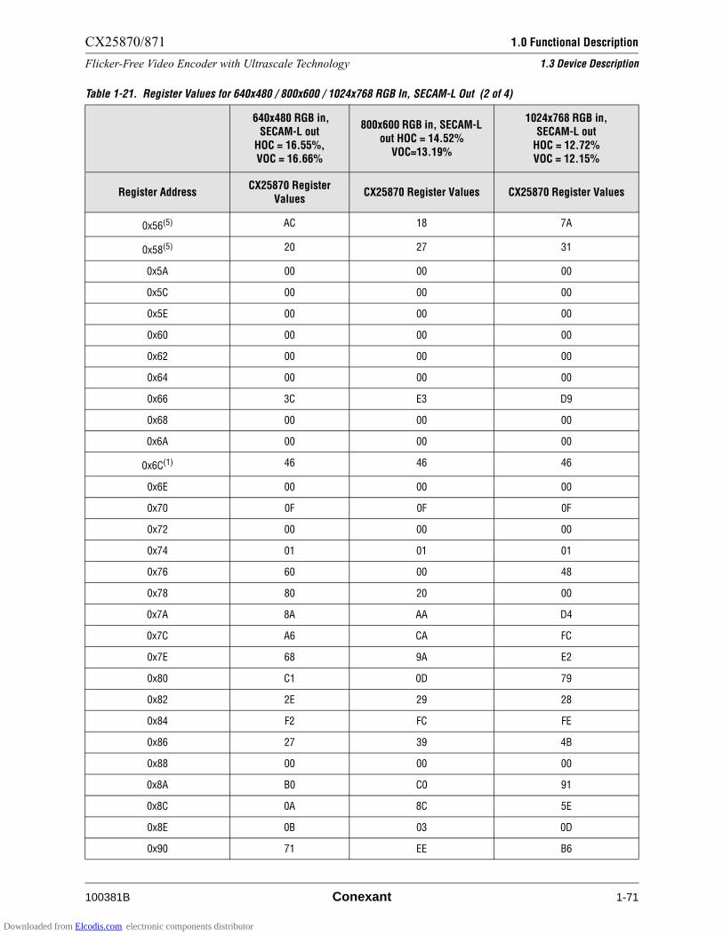
CX25870/871 1.0 Functional Description
Flicker-Free Video Encoder with Ultrascale Technology 1.3 Device Description
100381B Conexant 1-71
Register AddressCX25870 Register
ValuesCX25870 Register Values CX25870 Register Values
0x56(5) AC 18 7A
0x58(5) 20 27 31
0x5A 00 00 00
0x5C 00 00 00
0x5E 00 00 00
0x60 00 00 00
0x62 00 00 00
0x64 00 00 00
0x66 3C E3 D9
0x68 00 00 00
0x6A 00 00 00
0x6C(1) 46 46 46
0x6E 00 00 00
0x70 0F 0F 0F
0x72 00 00 00
0x74 01 01 01
0x76 60 00 48
0x78 80 20 00
0x7A 8A AA D4
0x7C A6 CA FC
0x7E 68 9A E2
0x80 C1 0D 79
0x82 2E 29 28
0x84 F2 FC FE
0x86 27 39 4B
0x88 00 00 00
0x8A B0 C0 91
0x8C 0A 8C 5E
0x8E 0B 03 0D
0x90 71 EE B6
Table 1-21. Register Values for 640x480 / 800x600 / 1024x768 RGB In, SECAM-L Out (2 of 4)
640x480 RGB in, SECAM-L out
HOC = 16.55%, VOC = 16.66%
800x600 RGB in, SECAM-L out HOC = 14.52%
VOC=13.19%
1024x768 RGB in, SECAM-L out
HOC = 12.72% VOC = 12.15%
Downloaded from Elcodis.com electronic components distributor
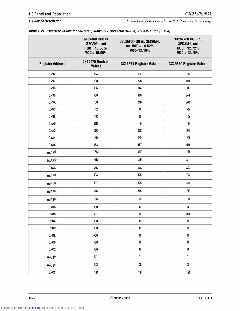
1.0 Functional Description CX25870/871
1.3 Device Description Flicker-Free Video Encoder with Ultrascale Technology
1-72 Conexant 100381B
Register AddressCX25870 Register
ValuesCX25870 Register Values CX25870 Register Values
0x92 5A 5F 76
0x94 E0 58 00
0x96 06 0A 3F
0x98 00 66 A4
0x9A 50 96 A0
0x9C 72 0 55
0x9E 1C 0 15
0xA0 0D 10 1E
0xA2 8C 8C 24
0xA4 F0 F0 F0
0xA6 58 57 56
0xA8(5) 76 5F 4B
0xAA(5) 4D 3E 31
0xAC 8C 8C 8C
0xAE(5) EA 55 76
0xB0(5) BE 55 4A
0xB2(5) 3C 55 FF
0xB4(5) 26 1F 18
0xB6 00 0 0
0xB8 01 3 33
0xBA 00 0 0
0xBC 00 0 0
0xBE 00 0 0
0xC0 00 0 0
0xC2 00 0 0
0xC4(2) 01 1 1
0xC6(3) 03 3 3
0xC8 1B 1B 1B
Table 1-21. Register Values for 640x480 / 800x600 / 1024x768 RGB In, SECAM-L Out (3 of 4)
640x480 RGB in, SECAM-L out
HOC = 16.55%, VOC = 16.66%
800x600 RGB in, SECAM-L out HOC = 14.52%
VOC=13.19%
1024x768 RGB in, SECAM-L out
HOC = 12.72% VOC = 12.15%
Downloaded from Elcodis.com electronic components distributor

CX25870/871 1.0 Functional Description
Flicker-Free Video Encoder with Ultrascale Technology 1.3 Device Description
100381B Conexant 1-73
The procedure required to obtain a SECAM output with an overscan
compensation percentage that differs from those solutions in Table 1-21 is fairly
simple. First, configure the encoder so it generates a standard PAL-B output with
the desired overscan compensation percentage. This can be done through the use
of an autoconfiguration mode, a hand-generated, or a predefined register set.
Second, perform a full register read-back from the CX25870. Carefully note the
value for register 0xA2. Third, program only the bits found in Table 1-22 to their
new state within the CX25870.
Register AddressCX25870 Register
ValuesCX25870 Register Values CX25870 Register Values
0xCA C0 C0 C0
0xCC C0 C0 C0
0xCE(4) 24 24 24
0xD0 00 0 0
0xD2 00 0 0
0xD4 00 0 0
0xD6 00 0 0
0xD8 40 40 40
NOTE(S):
1. Register 0x6C contains the TIMING_RESET bit. Set this bit as your last programming step and the CX25870 will clear it automatically later.
2. Register 0xC4 contains the EN_OUT bit. Adjust according to your design's interface as necessary.
3. Register 0xC6 contains the EN_BLANKO, EN_DOT, and IN_MODE[2:0] bits. Adjust according to your design's interface as necessary.
4. Register 0xCE contains the OUT_MUXD[1:0], OUTMUXC[1:0], OUTMUXB[1:0], and OUTMUXA[1:0] bit fields for output
routing. Adjust according to your design's interface as necessary.5. This is a SECAM specific register.
Table 1-21. Register Values for 640x480 / 800x600 / 1024x768 RGB In, SECAM-L Out (4 of 4)
640x480 RGB in, SECAM-L out
HOC = 16.55%, VOC = 16.66%
800x600 RGB in, SECAM-L out HOC = 14.52%
VOC=13.19%
1024x768 RGB in, SECAM-L out
HOC = 12.72% VOC = 12.15%
Table 1-22. Vital SECAM Bit Settings–Register 0xA2
Bit Name Location State for PAL-BDGHI State for SECAM
FM Bit 7 of register 0xA2 0 1
PAL_MD Bit 5 of register 0xA2 1 0
VSYNC_DUR Bit 3 of register 0xA2 0 0
Downloaded from Elcodis.com electronic components distributor
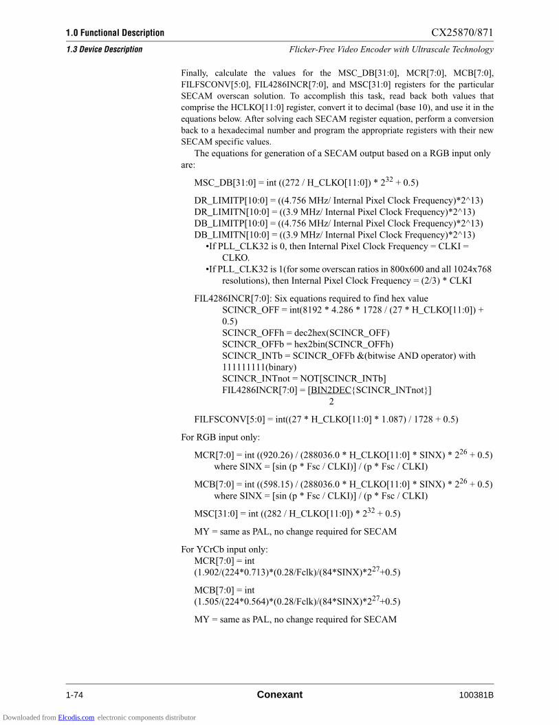
1.0 Functional Description CX25870/871
1.3 Device Description Flicker-Free Video Encoder with Ultrascale Technology
1-74 Conexant 100381B
Finally, calculate the values for the MSC_DB[31:0], MCR[7:0], MCB[7:0],
FILFSCONV[5:0], FIL4286INCR[7:0], and MSC[31:0] registers for the particular
SECAM overscan solution. To accomplish this task, read back both values that
comprise the HCLKO[11:0] register, convert it to decimal (base 10), and use it in the
equations below. After solving each SECAM register equation, perform a conversion
back to a hexadecimal number and program the appropriate registers with their new
SECAM specific values.
The equations for generation of a SECAM output based on a RGB input only
are:
MSC_DB[31:0] = int ((272 / H_CLKO[11:0]) * 232 + 0.5)
DR_LIMITP[10:0] = ((4.756 MHz/ Internal Pixel Clock Frequency)*2^13)
DR_LIMITN[10:0] = ((3.9 MHz/ Internal Pixel Clock Frequency)*2^13)
DB_LIMITP[10:0] = ((4.756 MHz/ Internal Pixel Clock Frequency)*2^13)
DB_LIMITN[10:0] = ((3.9 MHz/ Internal Pixel Clock Frequency)*2^13)
•If PLL_CLK32 is 0, then Internal Pixel Clock Frequency = CLKI =
CLKO.
•If PLL_CLK32 is 1(for some overscan ratios in 800x600 and all 1024x768
resolutions), then Internal Pixel Clock Frequency = (2/3) * CLKI
FIL4286INCR[7:0]: Six equations required to find hex value
SCINCR_OFF = int(8192 * 4.286 * 1728 / (27 * H_CLKO[11:0]) +
0.5)
SCINCR_OFFh = dec2hex(SCINCR_OFF)
SCINCR_OFFb = hex2bin(SCINCR_OFFh)
SCINCR_INTb = SCINCR_OFFb &(bitwise AND operator) with
111111111(binary)
SCINCR_INTnot = NOT[SCINCR_INTb]
FIL4286INCR[7:0] = [BIN2DECSCINCR_INTnot]
2
FILFSCONV[5:0] = int((27 * H_CLKO[11:0] * 1.087) / 1728 + 0.5)
For RGB input only:
MCR[7:0] = int ((920.26) / (288036.0 * H_CLKO[11:0] * SINX) * 226 + 0.5)
where SINX = [sin (p * Fsc / CLKI)] / (p * Fsc / CLKI)
MCB[7:0] = int ((598.15) / (288036.0 * H_CLKO[11:0] * SINX) * 226 + 0.5)
where SINX = [sin (p * Fsc / CLKI)] / (p * Fsc / CLKI)
MSC[31:0] = int ((282 / H_CLKO[11:0]) * 232 + 0.5)
MY = same as PAL, no change required for SECAM
For YCrCb input only:
MCR[7:0] = int
(1.902/(224*0.713)*(0.28/Fclk)/(84*SINX)*227+0.5)
MCB[7:0] = int
(1.505/(224*0.564)*(0.28/Fclk)/(84*SINX)*227+0.5)
MY = same as PAL, no change required for SECAM
Downloaded from Elcodis.com electronic components distributor
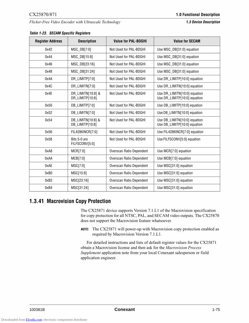
CX25870/871 1.0 Functional Description
Flicker-Free Video Encoder with Ultrascale Technology 1.3 Device Description
100381B Conexant 1-75
1.3.41 Macrovision Copy Protection
The CX25871 device supports Version 7.1.L1 of the Macrovision specification
for copy protection for all NTSC, PAL, and SECAM video outputs. The CX25870
does not support the Macrovision feature whatsoever.
NOTE: The CX25871 will power-up with Macrovision copy protection enabled as
required by Macrovision Version 7.1.L1.
For detailed instructions and lists of default register values for the CX25871
obtain a Macrovision license and then ask for the Macrovision Process
Supplement application note from your local Conexant salesperson or field
application engineer.
Table 1-23. SECAM Specific Registers
Register Address Description Value for PAL-BDGHI Value for SECAM
0x42 MSC_DB[7:0] Not Used for PAL-BDGHI Use MSC_DB[31:0] equation
0x44 MSC_DB[15:8] Not Used for PAL-BDGHI Use MSC_DB[31:0] equation
0x46 MSC_DB[23:16] Not Used for PAL-BDGHI Use MSC_DB[31:0] equation
0x48 MSC_DB[31:24] Not Used for PAL-BDGHI Use MSC_DB[31:0] equation
0x4A DR_LIMITP[7:0] Not Used for PAL-BDGHI Use DR_LIMITP[10:0] equation
0x4C DR_LIMITN[7:0] Not Used for PAL-BDGHI Use DR_LIMITN[10:0] equation
0x4E DR_LIMITN[10:8] &
DR_LIMITP[10:8]
Not Used for PAL-BDGHI Use DR_LIMITN[10:0] equation
Use DR_LIMITP[10:0] equation
0x50 DB_LIMITP[7:0] Not Used for PAL-BDGHI Use DB_LIMITP[10:0] equation
0x52 DB_LIMITN[7:0] Not Used for PAL-BDGHI Use DB_LIMITN[10:0] equation
0x54 DB_LIMITN[10:8] & DB_LIMITP[10:8]
Not Used for PAL-BDGHI Use DB_LIMITN[10:0] equation
Use DB_LIMITP[10:0] equation
0x56 FIL4286INCR[7:0] Not Used for PAL-BDGHI Use FIL4286INCR[7:0] equation
0x58 Bits 5-0 are FILFSCONV[5:0]
Not Used for PAL-BDGHI Use FILFSCONV[5:0] equation
0xA8 MCR[7:0] Overscan Ratio Dependent Use MCR[7:0] equation
0xAA MCB[7:0] Overscan Ratio Dependent Use MCB[7:0] equation
0xAE MSC[7:0] Overscan Ratio Dependent Use MSC[31:0] equation
0xB0 MSC[15:8] Overscan Ratio Dependent Use MSC[31:0] equation
0xB2 MSC[23:16] Overscan Ratio Dependent Use MSC[31:0] equation
0xB4 MSC[31:24] Overscan Ratio Dependent Use MSC[31:0] equation
Downloaded from Elcodis.com electronic components distributor
1.0 Functional Description CX25870/871
1.3 Device Description Flicker-Free Video Encoder with Ultrascale Technology
1-76 Conexant 100381B
1.3.42 HDTV Output Mode
The CX25870/871 includes an HDTV Output Mode that generates the analog
RGB or analog YPBPR component video outputs necessary for driving an
HDTV’s HD input port.
While generating HDTV outputs, the device accepts RGB or YPRPB digital
data in a 480p, 720p, or 1080i ATSC resolution. After a pipeline delay, it outputs
either analog RGB or analog YPBPR signals and automatically inserts trilevel
synchronization pulses (when necessary) and vertical synchronizing ‘broad
pulses’. The output waveforms, input data requirements and all configuration
details are explained in Appendix E. The device complies with all major SMPTE
and EIA standards governing the HDTV resolutions.
1.3.43 SCART Output
In this mode of operation, the CX25870/871 can be used successfully to provide
one full Red/Green/Blue/Composite (or optionally, a 2-signal Luminance and
Chrominance) SCART/Peritel output to drive SCART-compatible televisions or
VCRs. Many PAL/European TVs being manufactured now have SCART
compatible sockets, that allows the television and the set top box, graphics card,
or game console driving it to work in RGB color instead of the standard
composite. The picture quality for full SCART is significantly better due to the
individual RGB Composite signals being sent directly to the TV color guns. This
is opposed to the TV having to modulate and decode the RGB signals from
another color format. This ultimately yields a crisper picture.
On power-up, the CX25870/871 will output NTSC or PAL standard-definition
television outputs depending on the state of the PAL pin. To switch the device into
SCART Output Mode with three sync-less Red/Green/Blue (RGB) analog outputs
and a single Composite (CVBS) PAL video output from the fourth DAC, program
the encoder into a satisfactory PAL output mode and then perform the sequence
of serial writes found in Table 1-24.
Downloaded from Elcodis.com electronic components distributor

CX25870/871 1.0 Functional Description
Flicker-Free Video Encoder with Ultrascale Technology 1.3 Device Description
100381B Conexant 1-77
NOTE: No change to the incoming or outgoing HSYNC* and VSYNC* signal
frequencies are necessary for SCART generation. The sync rates should
continue to match those found with PAL-BDGHI transmission.
While the CX25870/871 is in SCART outmode, the composite video output
(Video[3]) contains a standard bilevel analog sync along with all other
components that comprise a standard PAL-BDGHI video signal. The sync pulse
has an amplitude of 0 mV to 300 mV peak-to-peak and a duration of 4.70 !s by
default. The amplitude can only be adjusted through the use of external passives,
but its width can be adjusted through serial writing of the CX25870
HSYNC_WIDTH register.
The CX25870’s Composite should be used by the subsystem to provide the
positive-going Video output/sync output expected by SCART-compliant display
devices. In other words, the PAL Composite output should be fed into the Video
Input (Contact #20-CEI IEC 933-1) on the SCART connector. CVBS will possess
the same bandwidth and time delays as the CX25870 RGB primary color signals.
The inclusion of a full composite video signal as the 4th output exceeds the
SCART capabilities of some non-Conexant Flicker Filter encoders which choose
to output only Composite Sync as the 4th output. This implementation benefits
the customer because some European Set-Top Boxes connect to TVs solely
through the SCART connector. If the TV only receives Composite video via the
SCART connector, and the Set Top Box is set to RGB output with sync for
blanking (not CVBS) on pin 20, a picture will not be present at all on the TV.
However, with the CX25870, if the TV only receives CVBS (not RGB) and the
Set Top Box is set to RGB output with CVBS on pin 20 the customer will get a
colorful picture on his TV.
Table 1-24. Serial Writes Required to Switch CX25870/871 into SCART Output Operation
Bit Name Location Value Comment
EN_SCART Bit 3–Register 0x6C 1 Enables SCART Output mode. DACs will transmit Video[0-3] as
SCART compatible RGB/CVBS outputs.
By default, in SCART Output mode, the CX25870 will transmit:
DAC_A = Video[0] = Red DAC_B = Video[1] = Green DAC_C = Video[2] = Blue
DAC_D = Video[3] = PAL Composite (CVBS)
OUT_MUXD[1:0]OUT_MUXC[1:0]OUT_MUXB[1:0]
OUT_MUXA[1:0]
Bits 7:0–Register CE E4 By configuring the DAC routing register, the CX25870 will now transmit: DAC_A = Video[0] = 00 = Red
DAC_B = Video[1] = 01 = Green DAC_C = Video[2] = 10 = Blue DAC_D = Video[3] = 11 = PAL Composite (CVBS)
OUT_MODE[1:0] Bits 3:2–Register D6 11 Forces CX25870 to generate SCART output mode.
Downloaded from Elcodis.com electronic components distributor
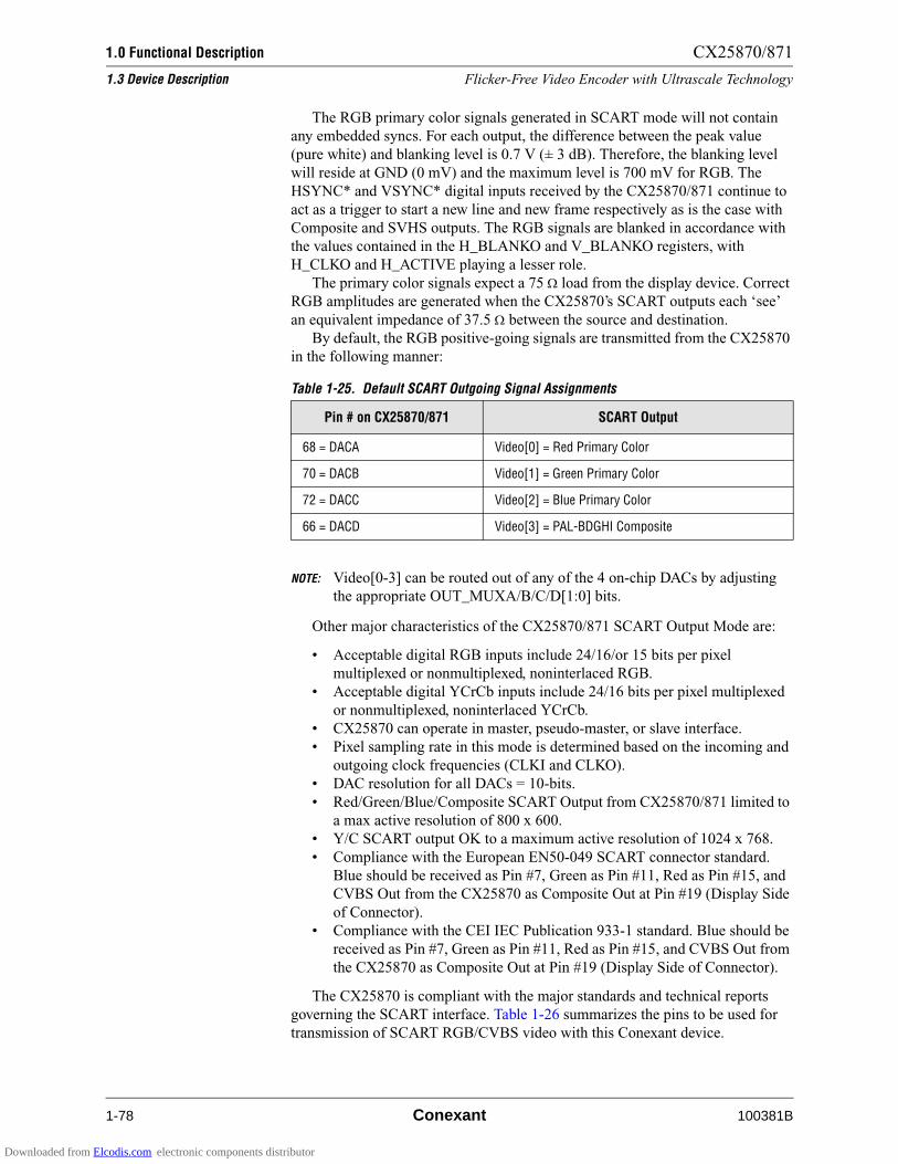
1.0 Functional Description CX25870/871
1.3 Device Description Flicker-Free Video Encoder with Ultrascale Technology
1-78 Conexant 100381B
The RGB primary color signals generated in SCART mode will not contain
any embedded syncs. For each output, the difference between the peak value
(pure white) and blanking level is 0.7 V (± 3 dB). Therefore, the blanking level
will reside at GND (0 mV) and the maximum level is 700 mV for RGB. The
HSYNC* and VSYNC* digital inputs received by the CX25870/871 continue to
act as a trigger to start a new line and new frame respectively as is the case with
Composite and SVHS outputs. The RGB signals are blanked in accordance with
the values contained in the H_BLANKO and V_BLANKO registers, with
H_CLKO and H_ACTIVE playing a lesser role.
The primary color signals expect a 75 " load from the display device. Correct
RGB amplitudes are generated when the CX25870’s SCART outputs each ‘see’
an equivalent impedance of 37.5 " between the source and destination.
By default, the RGB positive-going signals are transmitted from the CX25870
in the following manner:
NOTE: Video[0-3] can be routed out of any of the 4 on-chip DACs by adjusting
the appropriate OUT_MUXA/B/C/D[1:0] bits.
Other major characteristics of the CX25870/871 SCART Output Mode are:
• Acceptable digital RGB inputs include 24/16/or 15 bits per pixel
multiplexed or nonmultiplexed, noninterlaced RGB.
• Acceptable digital YCrCb inputs include 24/16 bits per pixel multiplexed
or nonmultiplexed, noninterlaced YCrCb.
• CX25870 can operate in master, pseudo-master, or slave interface.
• Pixel sampling rate in this mode is determined based on the incoming and
outgoing clock frequencies (CLKI and CLKO).
• DAC resolution for all DACs = 10-bits.
• Red/Green/Blue/Composite SCART Output from CX25870/871 limited to
a max active resolution of 800 x 600.
• Y/C SCART output OK to a maximum active resolution of 1024 x 768.
• Compliance with the European EN50-049 SCART connector standard.
Blue should be received as Pin #7, Green as Pin #11, Red as Pin #15, and
CVBS Out from the CX25870 as Composite Out at Pin #19 (Display Side
of Connector).
• Compliance with the CEI IEC Publication 933-1 standard. Blue should be
received as Pin #7, Green as Pin #11, Red as Pin #15, and CVBS Out from
the CX25870 as Composite Out at Pin #19 (Display Side of Connector).
The CX25870 is compliant with the major standards and technical reports
governing the SCART interface. Table 1-26 summarizes the pins to be used for
transmission of SCART RGB/CVBS video with this Conexant device.
Table 1-25. Default SCART Outgoing Signal Assignments
Pin # on CX25870/871 SCART Output
68 = DACA Video[0] = Red Primary Color
70 = DACB Video[1] = Green Primary Color
72 = DACC Video[2] = Blue Primary Color
66 = DACD Video[3] = PAL-BDGHI Composite
Downloaded from Elcodis.com electronic components distributor
CX25870/871 1.0 Functional Description
Flicker-Free Video Encoder with Ultrascale Technology 1.3 Device Description
100381B Conexant 1-79
A specialized cable and connector are required to connect the CX25870’s
RGB/CVBS or Y/C outputs to the TV’s SCART input. This cable can be procured
from various European electronic stores and comes in at least two different
arrangements. Consult the CEI IEC 933-1 specification (Audio, Video, and
Audiovisual systems-Interconnections and Matching Values) for a precise
illustration of their 21-contact SCART connector, video signal peak-peak values,
and cordset types.
The most common types of SCART connectors are the so-called Type I and
Type II variety. Figures 1-34 and 1-35 illustrate the recommended Type I and
Type II SCART connector pinout arrangements.
Table 1-26. CX25870 SCART Outputs for Different SCART Standards
RGB Standard Red Green Blue Composite/Blanking
European EN50-049 SCART (1) connector Pin 15 Pin 11 Pin 7 Pin 19 -Composite Out
(To Display)
CEI IEC 933-1 : (1) BBC SCART Arrangement #1 Pin 15 Pin 11 Pin 7 Pin 19 - Composite Out (To Display)
Y- C Standard Chroma x Luma x
Luminance - Chrominance (2) SCART: BBC SCART Arrangement #2
Pin 15 c Pin 20 —
NOTE(S):(1) Red/Green/Blue signals levels are from 0 V + 0.7 V peak-to-peak with 75 " load impedance.(2) The Luminance – Chrominance Outputs for SCART are equivalent to PAL-BDGHI S-Video. Therefore, OUTMODE[1:0] should
be programmed to 00, the EN_SCART bit should be reset to 0, and the OUTMUXA/B/C/D[1:0] bits adjusted according to
which DACs must transmit Luminance(Video[1]) and Chrominance(Video[2]).
Figure 1-34. CX25870 Driving a Type I SCART Connector (EN 50-049 and IEC 933-1 Compliant)
100381_092
CVBS as Sync
Y/R
C/G3.3 V
3.3 V
3.3 V
+3.3 V
3.3 V
21
19
17
15
13
11
9
7
5
3
1
20
18
16
14
12
10
8
6
4
2
CVBS/B
CX25870/871
Std DefLPF
SCARTConnector
Std DefLPF
Std DefLPF
Std DefLPF
75 "1%
75 "1%
75 "1%
75 "1%
Downloaded from Elcodis.com electronic components distributor

1.0 Functional Description CX25870/871
1.3 Device Description Flicker-Free Video Encoder with Ultrascale Technology
1-80 Conexant 100381B
Conexant recommends that any designer utilizing the CX25870 with either
type of SCART output utilize the same DAC low-pass filters used for standard
definition TV outputs listed in Chapter 3.0 of this data sheet.
1.3.44 Interlaced Standard Definition Analog Component Video TV Outputs
In this mode of operation, the CX25870/25871 provides a set of Component
Video Y, PB (B–Y), PR (R–Y) outputs based on a 480 line interlaced RGB or
YCrCb digital input format. Some DVD Players, such as those made by Toshiba
and Panasonic, call the Component Video Output format by their branded name,
“ColorStream.” Others refer to the two EIA standards governing this video
format–EIA-770.1 and EIA-770.2-A, and state this video type as Interlaced
Component Video, 480i Component Video, or Component YUV. Regardless of
the different names, the video format remains the same. For instructions on how
to configure the CX25870/871 to generate progressive 480p Component Video
(or ColorStream Pro), refer to that particular section in this data sheet.
The designer can enable ColorStream by using three of the CX25870’s DACs
to generate two color difference signals (PR and PB sometimes referred to as CR
and CB) and a single luminance signal (Y). These three channels allow the video
generating device to bypass the TV’s internal Y/C separator and color decoder
circuits. The analog information therefore gets routed directly into the TV’s
matrix decoder. By sending the pure component video signal directly to a
Component Video or ColorStream input-equipped display media, the input signal
forgoes the extra processing that normally would degrade the analog image.
Figure 1-35. CX25870 Driving a Type II SCART Connector (Y/C and BBC SCART Compliant)
100381_093
Y/R
C/G
3.3 V
+3.3 V
3.3 V
21
19
17
15
13
11
9
7
5
3
1
20
18
16
14
12
10
8
6
4
2
CVBS/B
CX25870/871
SCARTConnector
Std DefLPF
Std DefLPF
75 "1%
75 "1%
Downloaded from Elcodis.com electronic components distributor
CX25870/871 1.0 Functional Description
Flicker-Free Video Encoder with Ultrascale Technology 1.3 Device Description
100381B Conexant 1-81
The advantage of this type of video is increased image quality combined with
more lifelike colors and crisper detail. Because the video information is
transferred over three separate connecting cables instead of two (for S-Video) or
one (for Coaxial or RCA/Composite), 480i Component Video yields the best
standard definition TV quality available. However, because we are still dealing
with standard 480 line interlaced resolutions, this format remains inferior to
High-Definition TV.
Output devices used for generating this format include, but are not limited to,
Digital TV set top boxes, Satellite DBS Receiver Decoders, and DVD players.
Input media capable of decoding ColorStream include television receivers and/or
monitors.
While in the Component Video mode, all 10-bits of the CX25870’s D/A
converters are available for encoding. This results in a D/A conversion more
accurate than conventional 8-bit, 13.500 MHz systems. The end result is a more
artifact-free and clear image.
Some major characteristics governing the interlaced standard definition
television analog component video interface are as follows:
• The digital input stream can be received in a progressive (i.e.,
noninterlaced) format or interlaced format. Interlaced data must be
transmitted as ODD–EVEN–ODD … fields. The fields carry every other
scan line in succession with succeeding fields carrying the lines not
scanned by the previous field.
• Each field will be divided into an active picture area and a vertical
blanking interval (VBI). Similarly, each line will be divided into an active
pixel area and a horizontal blanking interval.
• The 480i video output will be capable of either a 4:3 or 16:9 aspect ratio
through embedding of Wide Screen Signaling (WSS) bits into the
appropriate lines in the VBI. Review the section 1.3.35 in the data sheet for
more details.
If configured properly, the CX25870’s EIA 770.2-A compliant Component
Video luminance signal has a peak amplitude of 700 mV from the blanking level,
with zero setup. A negative-going bilevel sync pulse of 300 mV, conforming to
the timing requirements in Figure 1.3-a, is added to the Luma signal as the only
timing reference for the complete Y PR PB set of signals.
Neither PR nor PB will contain an embedded sync pulse. Both will have a
maximum peak amplitude of ± 350 mV. The DC level of PR and PB during the
horizontal line shown in Figure 1-36 below will be at reference black with a
voltage of 0 V. It will be generated in conformance with the EIA 770.2-A and
EIA770.1 standards. The only differences between these standards are the
presence of the 7.5 IRE setup pedestal and slightly different luminance levels.
Check Tables 1-27 and 1-28 for complete programming instructions for either
standard.
Pixels per Active Line
Active Lines per Frame
Frame Rate(Hz)
Output Scanning Format
Total Samples per Line
Total Liens per Frame
720 480 30 / 1.001 Interlaced 858 525
Downloaded from Elcodis.com electronic components distributor
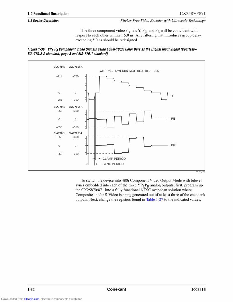
1.0 Functional Description CX25870/871
1.3 Device Description Flicker-Free Video Encoder with Ultrascale Technology
1-82 Conexant 100381B
The three component video signals Y, PB, and PR will be coincident with
respect to each other within ± 5.0 ns. Any filtering that introduces group delay
exceeding 5.0 ns should be redesigned.
To switch the device into 480i Component Video Output Mode with bilevel
syncs embedded into each of the three YPRPB analog outputs, first, program up
the CX25870/871 into a fully functional NTSC over-scan solution where
Composite and/or S-Video is being generated out of at least three of the encoder’s
outputs. Next, change the registers found in Table 1-27 to the indicated values.
Figure 1-36. YPR PB Component Video Signals using 100/0/100/0 Color Bars as the Digital Input Signal (Courtesy– EIA-770.2-A standard, page 8 and EIA-770.1 standard)
100381_098
CLAMP PERIOD
Y
PB
PR
SYNC PERIOD
WHT YEL CYN GRN MGT RED BLU BLK
EIA770.1 EIA770.2-A
EIA770.1 EIA770.2-A
EIA770.1 EIA770.2-A
+714 +700
+350 +350
+350 +350
0 0
0 0
0 0
–286 –300
–350 –350
–350 –350
Downloaded from Elcodis.com electronic components distributor
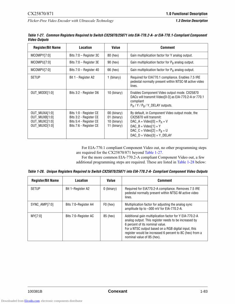
CX25870/871 1.0 Functional Description
Flicker-Free Video Encoder with Ultrascale Technology 1.3 Device Description
100381B Conexant 1-83
For EIA-770.1 compliant Component Video out, no other programming steps
are required for the CX25870/871 beyond Table 1-27.
For the more common EIA-770.2-A compliant Component Video out, a few
additional programming steps are required. These are listed in Table 1-28 below:
Table 1-27. Common Registers Required to Switch CX25870/25871 into EIA-770.2-A- or EIA-770.1-Compliant Component Video Outputs
Register/Bit Name Location Value Comment
MCOMPY[7:0] Bits 7:0 – Register 3C 80 (hex) Gain multiplication factor for Y analog output.
MCOMPU[7:0] Bits 7:0 – Register 3E 90 (hex) Gain multiplication factor for PB analog output.
MCOMPV[7:0] Bits 7:0 – Register 40 66 (hex) Gain multiplication factor for PR analog output.
SETUP Bit 1 - Register A2 1 (binary) Required for EIA770.1 compliance. Enables 7.5 IRE pedestal normally present within NTSC-M active video lines.
OUT_MODE[1:0] Bits 3:2 - Register D6 10 (binary) Enables Component Video output mode. CX25870
DACs will transmit Video[0-3] as EIA-770.2-A or 770.1 compliant PR / Y / PB / Y_DELAY outputs.
OUT_MUXA[1:0]OUT_MUXB[1:0]
OUT_MUXC[1:0]OUT_MUXD[1:0]
Bits 1:0 - Register CEBits 3:2 - Register CE
Bits 5:4 - Register CEBits 7:6 - Register CE
00 (binary)01 (binary)
10 (binary)11 (binary)
By default, in Component Video output mode, the CX25870 will transmit:
DAC_A = Video[0] = PR = V
DAC_B = Video[1] = Y
DAC_C = Video[2] = PB = U
DAC_D = Video[3] = Y_DELAY
Table 1-28. Unique Registers Required to Switch CX25870/25871 into EIA-770.2-A- Compliant Component Video Outputs
Register/Bit Name Location Value Comment
SETUP Bit 1–Register A2 0 (binary) Required for EIA770.2-A compliance. Removes 7.5 IRE
pedestal normally present within NTSC-M active video lines.
SYNC_AMP[7:0] Bits 7:0–Register A4 F0 (hex) Multiplication factor for adjusting the analog sync amplitude tip to –300 mV for EIA-770.2-A.
MY[7:0] Bits 7:0–Register AC 85 (hex) Additional gain multiplication factor for Y EIA-770.2-A analog output. This register needs to be increased by 6 percent of its nominal value.
For a NTSC output based on a RGB digital input, this register would be increased 6 percent to 8C (hex) from a nominal value of 85 (hex).
Downloaded from Elcodis.com electronic components distributor

1.0 Functional Description CX25870/871
1.3 Device Description Flicker-Free Video Encoder with Ultrascale Technology
1-84 Conexant 100381B
The analog Y, PB, and PR - Video[0-3] outputs can be routed out of any of the
four on-chip DACs by adjusting the appropriate OUT_MUXA/B/C/D[1:0] bits.
All of the OUT_MUX bits are contained in register 0xCE.
Because the CX25870 device has four DACs and only three are needed for
Component Video, the designer can choose to use the 4th output, usually from
DAC_D, for any purpose deemed necessary. This output can be configured to
either the PR, Y, PB, or Y_DELAY output via OUT_MUXD. If the output is not
going to be used whatsoever, Conexant recommends DAC_D be disabled by
setting DACDISD (bit 3, Register BA). This will save on power dissipation.
The Component Video output signals expect a 75 " load to ground from the
display medium. Correct Y, PR, PB amplitudes will be generated only when each
CX25870 output sees an equivalent impedance of 37.5 " between the source and
destination.
The CX25870 is compliant with the major standards and technical reports
governing the Standard Definition TV Analog Component Video interface. The
name of these standards are as follows:
• EIA 770.2-A–Standard Definition TV Analog Component Video Interface
• EIA 770.1–Standard Definition TV Analog Component Video Interface
• ANSI/SMPTE Standard 170M (1994) (M/NTSC) for
Television–Composite Analog Video Signal–NTSC for Studio
Applications
To obtain any of these specifications, visit Global Engineering Documents at:
http://global.ihs.com/
Conexant recommends that any designer utilizing the CX25870 with a
Component Video output utilize the same DAC low-pass filters used for standard
definition TV outputs listed in Figure 3-2 of this data sheet.
Downloaded from Elcodis.com electronic components distributor

CX25870/871 1.0 Functional Description
Flicker-Free Video Encoder with Ultrascale Technology 1.3 Device Description
100381B Conexant 1-85
1.3.45 VGA(RGB)—DAC Output Operation
In this mode of operation, the CX25870/871 acts as a general-purpose triple
high-speed D/A converter used to drive video receivers, such as PC monitors. The
encoder accomplishes this by bypassing most of the encoder blocks utilized for
television outputs, such as the Flicker Filter and FIFO and routing the RGB or
YCrCb digital data straight through to the on-chip 10-bit DACs. Once the data
arrives at the DACs, it is quickly converted to a set of 700 mV peak-to-peak
analog outputs, streamed through the respective DAC_X output pins, and routed
onto the rest of the graphics system according to the PCB layout.
Optimal performance is achieved when the CX25870/871’s current controlled
DACs are terminated into appropriate resistive loads to produce voltage outputs.
The chip’s DAC outputs are specifically designed to produce video output levels
with a total peak-peak active-region amplitude of 700 mV when directly
connected to a single-ended, doubly terminated (Req = 37.5 ") load. With the
recommended loading of two 75 " ± 1 percent resistors (one each for the
transmitting and receiving side), the full-scale video amplitude is from 286 mV
(blanking) to 986 mV (maximum luminance) and synchronization pulses from
0 mV (negative sync tip) to 286 mV (blanking) respectively. The analog
synchronization pulse is generated by the CX25870/871 every time it receives a
falling edge on either the HSYNC* or the VSYNC* input by default. These sync
pulses can be disabled for the RGB outputs by following the steps found in
Table 1-30.
On power-up, the CX25870/871 will output NTSC or PAL standard-definition
television outputs depending on the state of the PAL pin. To switch the device into
VGA-DAC Output Mode with bilevel syncs embedded on every Red/Green/Blue
(RGB) analog output, perform the sequence of serial writes found in Table 1-29
only.
Table 1-29. Serial Writes Required to Switch CX25870/871 into VGA/DAC Output Operation
Bit Name Location Value Comment
SLAVER Bit 5–Register 0xBA 1 Ensures CX25871 in slave or pseudo-master interface
EN_XCLK Bit 7–Register 0xA0 1 CLKI used as pixel clock source.
SETUP Bit 1–Register 0xA2 0 Setup off. The +56 mV pedestal setup is disabled for active
video lines.
OUT_MODE[1:0] Bits 3:2–Register D6 11 Video [0-3] = 11 = VGA Output Mode: DAC_A = Video[0] = Red
DAC_B = Video[1] = GreenDAC_C = Video[2] = Blue
DAC_DISD Bit 3–Register 0xBA 1 Disables DACD output. Current is set to 0 mA. Output voltage goes to 0 V.
Downloaded from Elcodis.com electronic components distributor
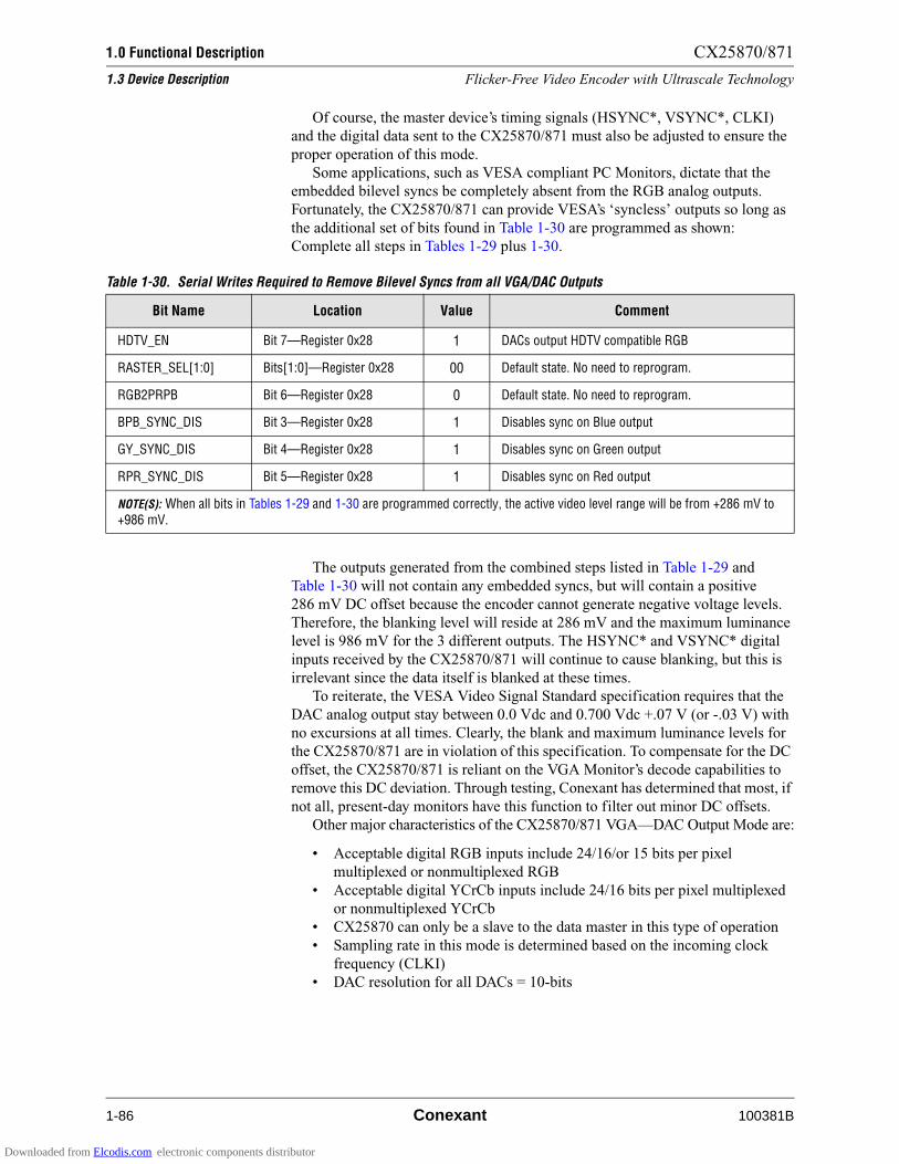
1.0 Functional Description CX25870/871
1.3 Device Description Flicker-Free Video Encoder with Ultrascale Technology
1-86 Conexant 100381B
Of course, the master device’s timing signals (HSYNC*, VSYNC*, CLKI)
and the digital data sent to the CX25870/871 must also be adjusted to ensure the
proper operation of this mode.
Some applications, such as VESA compliant PC Monitors, dictate that the
embedded bilevel syncs be completely absent from the RGB analog outputs.
Fortunately, the CX25870/871 can provide VESA’s ‘syncless’ outputs so long as
the additional set of bits found in Table 1-30 are programmed as shown:
Complete all steps in Tables 1-29 plus 1-30.
The outputs generated from the combined steps listed in Table 1-29 and
Table 1-30 will not contain any embedded syncs, but will contain a positive
286 mV DC offset because the encoder cannot generate negative voltage levels.
Therefore, the blanking level will reside at 286 mV and the maximum luminance
level is 986 mV for the 3 different outputs. The HSYNC* and VSYNC* digital
inputs received by the CX25870/871 will continue to cause blanking, but this is
irrelevant since the data itself is blanked at these times.
To reiterate, the VESA Video Signal Standard specification requires that the
DAC analog output stay between 0.0 Vdc and 0.700 Vdc +.07 V (or -.03 V) with
no excursions at all times. Clearly, the blank and maximum luminance levels for
the CX25870/871 are in violation of this specification. To compensate for the DC
offset, the CX25870/871 is reliant on the VGA Monitor’s decode capabilities to
remove this DC deviation. Through testing, Conexant has determined that most, if
not all, present-day monitors have this function to filter out minor DC offsets.
Other major characteristics of the CX25870/871 VGA—DAC Output Mode are:
• Acceptable digital RGB inputs include 24/16/or 15 bits per pixel
multiplexed or nonmultiplexed RGB
• Acceptable digital YCrCb inputs include 24/16 bits per pixel multiplexed
or nonmultiplexed YCrCb
• CX25870 can only be a slave to the data master in this type of operation
• Sampling rate in this mode is determined based on the incoming clock
frequency (CLKI)
• DAC resolution for all DACs = 10-bits
Table 1-30. Serial Writes Required to Remove Bilevel Syncs from all VGA/DAC Outputs
Bit Name Location Value Comment
HDTV_EN Bit 7—Register 0x28 1 DACs output HDTV compatible RGB
RASTER_SEL[1:0] Bits[1:0]—Register 0x28 00 Default state. No need to reprogram.
RGB2PRPB Bit 6—Register 0x28 0 Default state. No need to reprogram.
BPB_SYNC_DIS Bit 3—Register 0x28 1 Disables sync on Blue output
GY_SYNC_DIS Bit 4—Register 0x28 1 Disables sync on Green output
RPR_SYNC_DIS Bit 5—Register 0x28 1 Disables sync on Red output
NOTE(S): When all bits in Tables 1-29 and 1-30 are programmed correctly, the active video level range will be from +286 mV to +986 mV.
Downloaded from Elcodis.com electronic components distributor

CX25870/871 1.0 Functional Description
Flicker-Free Video Encoder with Ultrascale Technology 1.3 Device Description
100381B Conexant 1-87
Finally, Conexant recommends that any designer utilizing the CX25870 in this
mode circumvent the three capacitors and one inductor found in the DAC
low-pass filters used for standard definition TV outputs. Figure 1-37 illustrates
one method of bypassing the capacitors and inductor. Note that an additional
RCA (or other type) of connector is recommended in this case for the Red. Green,
and Blue VGA Outputs.
Figure 1-37. Filterless DAC Outputs for VGA (RGB)—DAC Output Operation
100381_083
68
CX25870/871In VGA Output Mode
DACA
DACB
DACC
DAC A
CVBS =Composite
DAC B
DAC C
70
72
VAA3.3 V
1
1
2
2
3
3
1
2
3
D6BAT54SSOT-23
5443R10-0041
R175.0 "08055%
C9270 pF08055%
C822 pF08055%
AOUT
VGA ROutput
C10330 pF08055%
L11.8 µH12105%
DAC B
Y = Luma
C = Chroma
VAA3.3 V
1
1
2
23
3
1
2
3
D6BAT54SSOT-23
5443R10-0041
R275.0 "08055%
C13270 pF08055%
C1222 pF08055%
BOUT
VGA GOutput
C14330 pF08055%
L31.8 µH12105%
DAC B
VAA3.3 V
1
1
2
2
3
3
1
2
3
D6BAT54SSOT-23
5443R10-0041
R775.0 "08055%
C16270 pF08055%
C1522 pF08055%
COUT
VGA BOutput
C17330 pF08055%
L21.8 µH12105%
NOTE(S):Make sure to have only one of the paired outputs plugged in simultaneously.
Downloaded from Elcodis.com electronic components distributor

1.0 Functional Description CX25870/871
1.3 Device Description Flicker-Free Video Encoder with Ultrascale Technology
1-88 Conexant 100381B
1.3.46 TV Auto-Detection Procedures
The device can determine whether or not the DAC output is connected to a
monitor by verifying that the output is doubly-terminated. The MONSTATx bit
for the corresponding DAC is set to a 1 if the device senses a doubly-terminated
load on a reset condition or if the CHECK_STAT register bit is set. While
CHECK_STAT is set, the output is forced to 2/3 of VREF when terminated and
4/3 of VREF if unterminated. The MONSTATx bit reflects the condition when the
DAC output is less than or equal to VREF. The CHECK_STAT bit is
automatically cleared after two clock cycles.
The CX25870/871 can be read from using 2 different methods. The first
method is called Standard serial read-back. To perform a read, simply have the
master device issue the CX25870/871’s serial device address (0x89 or 0x8B
depending on the state of the encoders ALTADDR pin), transmit the particular
subaddress (encoder register index) to read from, and then wait for the
CX25870/871 to transmit the appropriate 8-bits of data. Of course, START and
STOP conditions and ACKs must exist at the pertinent times as well, but this
summarizes the basic procedure.
The second method that can be used to read back from the encoder is called
the Legacy method. This is because the procedure that follows was the only
manner in which Conexant’s first generation encoder (i.e., Bt868/869) could be
read from. For compatibility purposes, this method was carried forward and exists
in this second generation encoder.
The Legacy procedure to follow for serial read-back and TV detection purposes
is:
1. Write 01 to the ESTATUS[1:0]bits D7=msb and D6 of register 0xC4bit
field. This sets up the encoder to read the MONSTAT data and check if the
DACs have a TV connected.
2. Write the CHECK_STAT register bit to a one (bit D6 of register BA). This
will latch the MONSTAT data internally and then clear itself.
3. Wait 600 µs to allow the analog nodes to reach their operating point.
4. Read the MONSTAT data by issuing 0x89 or 0x8B for the CX25870/871’s
device address. This ensures the least significant bit of the device write
portion of the transaction is 1, which indicates to the encoder that it must
send a byte of data on the next serial transaction. Do not write a subaddress
to the encoder (this is not necessary since the first generation encoder only
had one read register) and then read the next byte after the ACK. The 8-bit
read in Step 1 contains either the CX25870’s ID&VERSION (if ESTATUS
was written to 00) or the CX25870’s Monitor Detection for DACs C, B,
and A + Closed Caption Status info and the FIELD # (if ESTATUS = 01).
If ESTATUS was written to 10 in Step 1, the read byte will contain the
PLL_LOCK, FIFO status bits, PAL bit, and BUSY bit.
Downloaded from Elcodis.com electronic components distributor

CX25870/871 1.0 Functional Description
Flicker-Free Video Encoder with Ultrascale Technology 1.3 Device Description
100381B Conexant 1-89
Table 1-31 summarizes the meaning of the read-back bits when the agency procedure
is used and ESTATUS[1:0] = 10, 01, or 00.
5. If ESTATUS = 01, the serial master should receive one byte of information
telling it the following information in this order:
a. Monitor Connection Status for DACA output (MONSTAT_A = most
significant bit).
b. Monitor Connection Status for DACB output (MONSTAT_B).
c. Monitor Connection Status for DACC output (MONSTAT_C).
d. CCSTAT_E, CCSTAT_O.
e. FIELD2, FIELD1, FIELD0 (least significant bit). The FIELD[2:0] bits
indicate the field number that was last encoded. 000 indicates the 1st
field.
6. The serial master must issue a STOP condition to finish the Read
transaction. An ACK is not necessary before closing the transaction
because the CX25870 just ignores the ACK anyway. In reality, the
CX25870/871 does not really care about ending a transaction properly as
long as a proper START condition is used to start the next transaction. In
the read mode when the CX25870 is driving the SDA port, ending the
transaction cannot take place until the encoder releases control of the SID
line. This happens during the transition from when the last bit of the
register is output to the receiving of the ACK.
7. The graphics controller, acting as the serial master, should clear the
CHECK_STAT register bit back to 0 (bit D6 of register BA) by writing
zero to the CHECK_STAT register bit (bit D6 of register BA) to display
standard video again from the CX25870/871 VGA encoder.
To reiterate, a START condition needs to be issued by the serial master to start
the next transaction. In the read mode, when the CX25870/871 is driving the SID
port, an end to the transaction cannot take place until the encoder releases control
of the SID line. This event happens during the transition from when the last bit of
the register is output to the receiving of the ACK.
Table 1-31. ESTATUS[1:0] Read-back Bit Map
ESTATUS [1:0]
7 6 5 4 3 2 1 0
00 ID[2:0] VERSION[4:0]
01 MONSTAT_A MONSTAT_B MONSTAT_C CCSTAT_E CCSTAT_O FIELD[2:0]
10 Reserved SECAM PLL_RESET_O
UT
PLL_LOCK FIFO_OVER FIFO_
UNDER
PAL RESERVED
NOTE(S): Descriptions of these bits are found in Table 2-4.
Downloaded from Elcodis.com electronic components distributor
1.0 Functional Description CX25870/871
1.3 Device Description Flicker-Free Video Encoder with Ultrascale Technology
1-90 Conexant 100381B
1.3.47 Sleep/Power Management
There are a number of sleep/power down options for the CX25870/871. These
options can be grouped into three different categories. The first category pertains
to power management during normal operation.
• DIS_PLL bit:
In nonsleep mode, when an external clock is being used, and the PLL is not
needed, this bit will disable the PLL function.
• XTAL_PAD_DIS bit:
Setting this bit forces the crystal oscillator circuit to completely shut down.
This requires the CX25870/871 to switch over to an external clock or the
RESET* pin needs to be pulsed low to recover.
• XTL_BFO_DIS bit:
This disables the crystal buffer when it is not needed.
• DIS_CLKO bit:
This will disable the CLKO output pin when not needed, i.e., an external
clock is used in slave interface or to reduce sleep current.
• DACDISx/DACOFF bits:
Each individual DAC can be powered down by setting its corresponding
DACDISx bit. This is useful only if some of the DACs are not being
utilized by the graphics system. The entire analog subsection of the device
can be powered-down with the DACOFF bit, allowing digital operations to
continue while reducing the power in the analog circuitry. This will achieve
a significant reduction in power while maintaining all digital functionality.
The second category pertains to software enabled sleep operation.
• SLEEP_EN bit:
Shuts down all internal clocks except the serial port interface clock.
Disables all digital I/O pins except these: SLEEP, ALTADDR, CLKI,
CLKO, and XTAL_OUT. Disables the PLL. Turns off all DACs and
VREF; SLEEP and RESET* are never disabled.
• PLL_KEEP_ALIVE bit:
When the PLL is used to provide a system clock, this bit keeps it
functioning if the rest of the chip is slept through either the sleep pin or
sleep bit. This bit has no affect if DIS_PLL is set.
• DIS_CLKI bit:
The disable for the CLKI is separate from the sleep bit and sleep pin to
accommodate using an external clock as the clock source for the
CX25870/871 or as the PLL input.
The third category relates to the pin driven sleep operation.
• SLEEP pin:
In addition to what the SLEEP_EN bit does, the sleep pin shuts down the
serial port interface and disables the ALTADDR pin. If the SLEEP pin = 1,
the only way the encoder can return to normal operation is by resetting the
SLEEP pin in 0.
To achieve additional power savings, all the power management options
available in normal operation are also available in software or pin driven sleep
operation.
For the lowest possible power consumption, set the XTL_BFO_DIS,
DIS_CLKO, DIS_CLKI, and XTAL_PAD_DIS bits in order, then pull the SLEEP
pin (#52) high.
Downloaded from Elcodis.com electronic components distributor
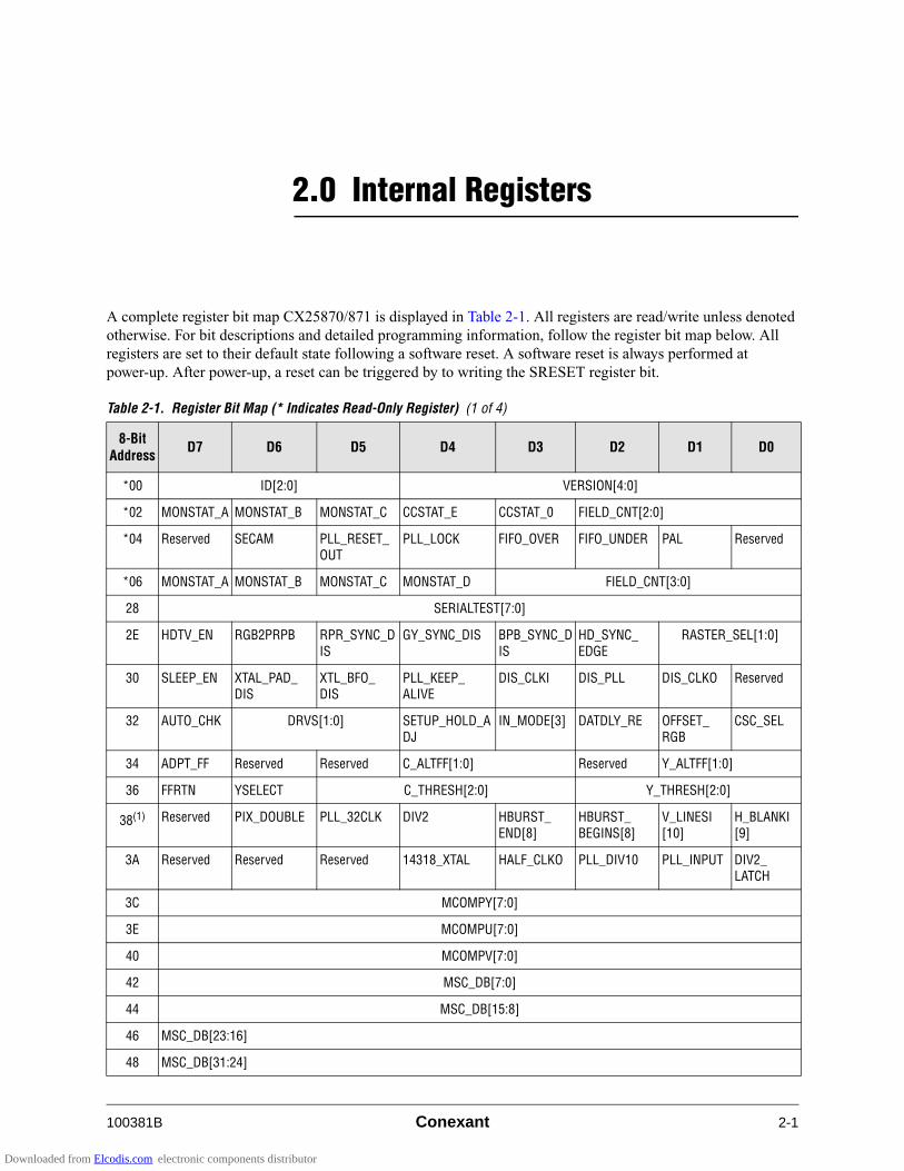
100381B Conexant 2-1
2
2.0 Internal Registers
A complete register bit map CX25870/871 is displayed in Table 2-1. All registers are read/write unless denoted
otherwise. For bit descriptions and detailed programming information, follow the register bit map below. All
registers are set to their default state following a software reset. A software reset is always performed at
power-up. After power-up, a reset can be triggered by to writing the SRESET register bit.
Table 2-1. Register Bit Map (* Indicates Read-Only Register) (1 of 4)
8-Bit Address
D7 D6 D5 D4 D3 D2 D1 D0
*00 ID[2:0] VERSION[4:0]
*02 MONSTAT_A MONSTAT_B MONSTAT_C CCSTAT_E CCSTAT_0 FIELD_CNT[2:0]
*04 Reserved SECAM PLL_RESET_OUT
PLL_LOCK FIFO_OVER FIFO_UNDER PAL Reserved
*06 MONSTAT_A MONSTAT_B MONSTAT_C MONSTAT_D FIELD_CNT[3:0]
28 SERIALTEST[7:0]
2E HDTV_EN RGB2PRPB RPR_SYNC_D
IS
GY_SYNC_DIS BPB_SYNC_D
IS
HD_SYNC_
EDGE
RASTER_SEL[1:0]
30 SLEEP_EN XTAL_PAD_ DIS
XTL_BFO_ DIS
PLL_KEEP_ ALIVE
DIS_CLKI DIS_PLL DIS_CLKO Reserved
32 AUTO_CHK DRVS[1:0] SETUP_HOLD_ADJ
IN_MODE[3] DATDLY_RE OFFSET_ RGB
CSC_SEL
34 ADPT_FF Reserved Reserved C_ALTFF[1:0] Reserved Y_ALTFF[1:0]
36 FFRTN YSELECT C_THRESH[2:0] Y_THRESH[2:0]
38(1) Reserved PIX_DOUBLE PLL_32CLK DIV2 HBURST_
END[8]
HBURST_
BEGINS[8]
V_LINESI
[10]
H_BLANKI
[9]
3A Reserved Reserved Reserved 14318_XTAL HALF_CLKO PLL_DIV10 PLL_INPUT DIV2_ LATCH
3C MCOMPY[7:0]
3E MCOMPU[7:0]
40 MCOMPV[7:0]
42 MSC_DB[7:0]
44 MSC_DB[15:8]
46 MSC_DB[23:16]
48 MSC_DB[31:24]
Downloaded from Elcodis.com electronic components distributor
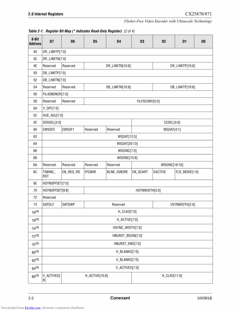
2.0 Internal Registers CX25870/871
Flicker-Free Video Encoder with Ultrascale Technology
2-2 Conexant 100381B
4A DR_LIMITP[7:0]
4C DR_LIMITN[7:0]
4E Reserved Reserved DR_LIMITN[10:8] DR_LIMITP[10:8]
50 DB_LIMITP[7:0]
52 DB_LIMITN[7:0]
54 Reserved Reserved DB_LIMITN[10:8] DB_LIMITP[10:8]
56 FIL4286INCR[7:0]
58 Reserved Reserved FILFSCONV[5:0]
5A Y_OFF[7:0]
5C HUE_ADJ[7:0]
5E XDSSEL[3:0] CCSEL[3:0]
60 EWSSF2 EWSSF1 Reserved Reserved WSDAT[4:1]
62 WSDAT[12:5]
64 WSDAT[20:13]
66 WSSINC[7:0]
68 WSSINC[15:8]
6A Reserved Reserved Reserved Reserved WSSINC[19:16]
6C TIMING_
RST
EN_REG_RD FFCBAR BLNK_IGNORE EN_SCART EACTIVE FLD_MODE[1:0]
6E HSYNOFFSET[7:0]
70 HSYNOFFSET[9:8] HSYNWIDTH[5:0]
72 Reserved
74 DATDLY DATSWP Reserved VSYNWIDTH[2:0]
76(1) H_CLKO[7:0]
78(1) H_ACTIVE[7:0]
7A(1) HSYNC_WIDTH[7:0]
7C(1) HBURST_BEGIN[7:0]
7E(1) HBURST_END[7:0]
80(1) H_BLANKO[7:0]
82(1) V_BLANKO[7:0]
84(1) V_ACTIVEO[7:0]
86(1) V_ACTIVEO[8]
H_ACTIVE[10:8] H_CLKO[11:8]
Table 2-1. Register Bit Map (* Indicates Read-Only Register) (2 of 4)
8-Bit Address
D7 D6 D5 D4 D3 D2 D1 D0
Downloaded from Elcodis.com electronic components distributor
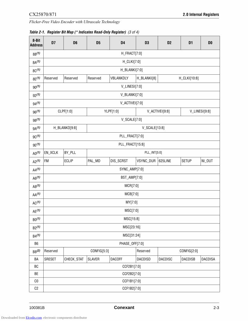
CX25870/871 2.0 Internal Registers
Flicker-Free Video Encoder with Ultrascale Technology
100381B Conexant 2-3
88(1) H_FRACT[7:0]
8A(1) H_CLKI[7:0]
8C(1) H_BLANKI[7:0]
8E(1) Reserved Reserved Reserved VBLANKDLY H_BLANKI[8] H_CLKI[10:8]
90(1) V_LINESI[7:0]
92(1) V_BLANKI[7:0]
94(1) V_ACTIVEI[7:0]
96(1) CLPF[1:0] YLPF[1:0] V_ACTIVEI[9:8] V_LINESI[9:8]
98(1) V_SCALE[7:0]
9A(1) H_BLANKO[9:8] V_SCALE[13:8]
9C(1) PLL_FRACT[7:0]
9E(1) PLL_FRACT[15:8]
A0(1) EN_XCLK BY_PLL PLL_INT[5:0]
A2(1) FM ECLIP PAL_MD DIS_SCRST VSYNC_DUR 625LINE SETUP NI_OUT
A4(1) SYNC_AMP[7:0]
A6(1) BST_AMP[7:0]
A8(1) MCR[7:0]
AA(1) MCB[7:0]
AC(1) MY[7:0]
AE(1) MSC[7:0]
B0(1) MSC[15:8]
B2(1) MSC[23:16]
B4(1) MSC[31:24]
B6 PHASE_OFF[7:0]
B8(2) Reserved CONFIG[5:3] Reserved CONFIG[2:0]
BA SRESET CHECK_STAT SLAVER DACOFF DACDISD DACDISC DACDISB DACDISA
BC CCF2B1[7:0]
BE CCF2B2[7:0]
C0 CCF1B1[7:0]
C2 CCF1B2[7:0]
Table 2-1. Register Bit Map (* Indicates Read-Only Register) (3 of 4)
8-Bit Address
D7 D6 D5 D4 D3 D2 D1 D0
Downloaded from Elcodis.com electronic components distributor
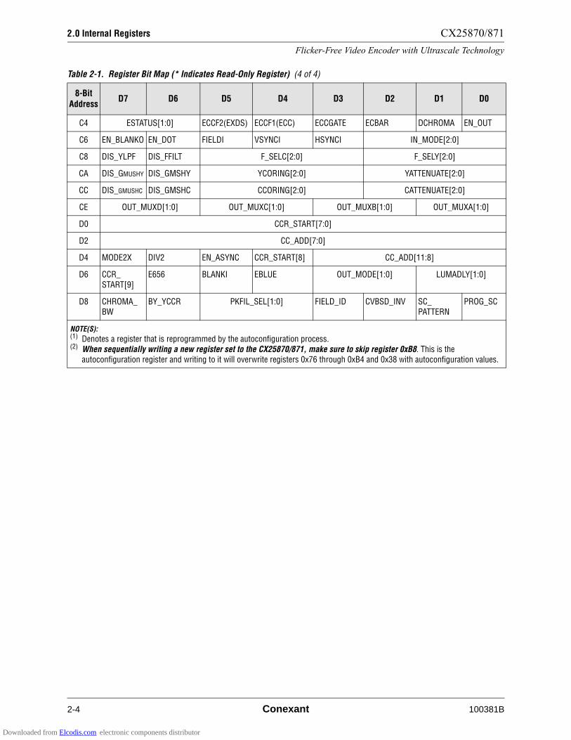
2.0 Internal Registers CX25870/871
Flicker-Free Video Encoder with Ultrascale Technology
2-4 Conexant 100381B
C4 ESTATUS[1:0] ECCF2(EXDS) ECCF1(ECC) ECCGATE ECBAR DCHROMA EN_OUT
C6 EN_BLANKO EN_DOT FIELDI VSYNCI HSYNCI IN_MODE[2:0]
C8 DIS_YLPF DIS_FFILT F_SELC[2:0] F_SELY[2:0]
CA DIS_GMUSHY DIS_GMSHY YCORING[2:0] YATTENUATE[2:0]
CC DIS_GMUSHC DIS_GMSHC CCORING[2:0] CATTENUATE[2:0]
CE OUT_MUXD[1:0] OUT_MUXC[1:0] OUT_MUXB[1:0] OUT_MUXA[1:0]
D0 CCR_START[7:0]
D2 CC_ADD[7:0]
D4 MODE2X DIV2 EN_ASYNC CCR_START[8] CC_ADD[11:8]
D6 CCR_
START[9]
E656 BLANKI EBLUE OUT_MODE[1:0] LUMADLY[1:0]
D8 CHROMA_ BW
BY_YCCR PKFIL_SEL[1:0] FIELD_ID CVBSD_INV SC_ PATTERN
PROG_SC
NOTE(S):(1) Denotes a register that is reprogrammed by the autoconfiguration process.(2) When sequentially writing a new register set to the CX25870/871, make sure to skip register 0xB8. This is the
autoconfiguration register and writing to it will overwrite registers 0x76 through 0xB4 and 0x38 with autoconfiguration values.
Table 2-1. Register Bit Map (* Indicates Read-Only Register) (4 of 4)
8-Bit Address
D7 D6 D5 D4 D3 D2 D1 D0
Downloaded from Elcodis.com electronic components distributor
CX25870/871 2.0 Internal Registers
Flicker-Free Video Encoder with Ultrascale Technology 2.1 Essential Registers
100381B Conexant 2-5
2.1 Essential Registers
The power-up state will be either autoconfiguration mode 0 (640 x 480 RGB in NTSC out) or autoconfiguration
mode 1 (640 x 480 RGB in, PAL_BDGHI out) depending on the state of the PAL pin. By default, the
CX25870/871 will be in master interface. To enable active video, the EACTIVE register bit must be set.
2.2 Device Address
The serial device address for the CX25870/871 is configurable by the state of the ALTADDR pin at reset.
Table 2-2 lists how the ALTADDR pin switches the devices serial address. The ALTADDR pins state should
only be changed during power-up.
2.3 Writing Registers
Following a start condition, writing 0x88 as the device ID initiates write access to the CX25870/871 registers
when the ALTADDR pin is low. Alternative device ID 0x8A initiates write access when the ALTADDR pin is
high. If the data is written sequentially in subaddress order, only the first subaddress needs to be written; the
internal address counter will automatically increment after each write to the next register.
When writing an entirely new register set to the CX25870/871, make sure to skip register 0xB8. This is the
autoconfiguration register, and writing any value to it after having loaded values into other registers will replace
desired data with unwanted data.
Table 2-2. Serial Address Configuration
ALTADDR State Device Address for Writing Device Address for Reading
0 0x88 0x89
1 0x8A 0x8B
Downloaded from Elcodis.com electronic components distributor

2.0 Internal Registers CX25870/871
2.4 Reading Registers Flicker-Free Video Encoder with Ultrascale Technology
2-6 Conexant 100381B
2.4 Reading Registers
Following a start condition, writing 0x89 and then the desired subaddress initiates the read-back sequence. The
next eight bits of information, returned by the CX25870/871, can be read from the SID pin, most significant bit
first. Alternative address 0x8B is required if the ALTADDR pin is high. Registers 0x00 through 0x06 are read
only. All other registers can be read from or written to.
The ID[2:0] bits of register 0x00 indicate the part type (CX25870/871 or Bt868/869). The lower five bits
(VERSION[4:0]) indicate the version number of that particular encoder.
For software detection of a connected TV monitor on each DAC output, the MONSTAT_x bits (found in
0x06 and 0x02 for legacy purposes) should be read accordingly after writing to CHECK_STAT. For a
description of this process follow the guidelines contained in the Section 1.3.46.
To check the status of the monitor connections at the DAC output automatically once per frame during the
vertical blanking interval, set the AUTO_CHK bit.
The following pseudocode sample should be used for properly reading registers within the CX25870/871.
First, there are some basic action assignments:
• Next, load 46 hex into register 6C. This will write the EN_REG_RD bit to 1. This enables the serial
master to read back all encoder registers.
Perform the following transaction with the serial master:
– START/D_ADDR/S_ACK/6C/S_ACK/46/S_ACK/STOP
• Next, use the serial master to write the register address from which read-back will occur:
– START/D_ADDR/S_ACK/<read_address>/S_ACK/STOP
Finally, read the data starting at the read_address previously issued:
– START/D_ADDR+1/S_ACK/<readdata(0)>/M_ACK/<readdata(1)>/M_
ACK/
<readdata(2)>/M_ACK/.../.../<readdata(n-1)>/M_ACK/<readdata(n)>/
NACK/STOP
where:
readdata(0) is the data from CX25870/871 register <read_address>
readdata(1) is the data from CX25870/871 register <read_address>+1
readdata(2) is the data from CX25870/871 register <read_address>+2
As long as the CX25870/871 detects an acknowledge from the serial master (M_ACK) after providing the
readdata, it will expect the read transaction to continue.
When no acknowledge is received, the encoder will end the read operation. Using this approach, consecutive
register reads can be provided with less software overhead.
To read just one register location, every programming step remains the same up to the point where the read
data transaction occurs.
S_ACK The slave device generates the acknowledge (i.e., the CX25870/871)
M_ACK The serial master generates the acknowledge.
NACK No acknowledge is generated by either device.
START Serial start condition; falling edge of SID occurs when SIC is high.
STOP Serial stop condition; rising edge of SID occurs when SIC is high.
D_ADDR The device address is 88 hex with ALTADDR = 0, 8A when it is a 1.
Downloaded from Elcodis.com electronic components distributor
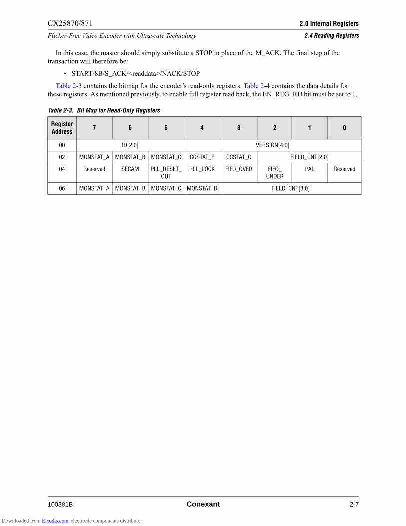
CX25870/871 2.0 Internal Registers
Flicker-Free Video Encoder with Ultrascale Technology 2.4 Reading Registers
100381B Conexant 2-7
In this case, the master should simply substitute a STOP in place of the M_ACK. The final step of the
transaction will therefore be:
• START/8B/S_ACK/<readdata>/NACK/STOP
.Table 2-3 contains the bitmap for the encoder’s read-only registers. Table 2-4 contains the data details for
these registers. As mentioned previously, to enable full register read back, the EN_REG_RD bit must be set to 1.
Table 2-3. Bit Map for Read-Only Registers
Register Address
7 6 5 4 3 2 1 0
00 ID[2:0] VERSION[4:0]
02 MONSTAT_A MONSTAT_B MONSTAT_C CCSTAT_E CCSTAT_O FIELD_CNT[2:0]
04 Reserved SECAM PLL_RESET_
OUT
PLL_LOCK FIFO_OVER FIFO_
UNDER
PAL Reserved
06 MONSTAT_A MONSTAT_B MONSTAT_C MONSTAT_D FIELD_CNT[3:0]
Downloaded from Elcodis.com electronic components distributor
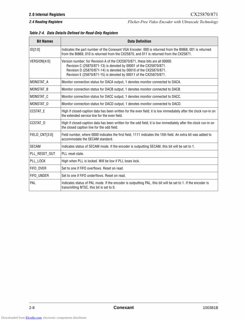
2.0 Internal Registers CX25870/871
2.4 Reading Registers Flicker-Free Video Encoder with Ultrascale Technology
2-8 Conexant 100381B
Table 2-4. Data Details Defined for Read-Only Registers
Bit Names Data Definition
ID[2:0] Indicates the part number of the Conexant VGA Encoder: 000 is returned from the Bt868, 001 is returned from the Bt869, 010 is returned from the CX25870, and 011 is returned from the CX25871.
VERSION[4:0] Version number; for Revision A of the CX25870/871, these bits are all 00000.
Revision C (25870/871-13) is denoted by 00001 of the CX25870/871.Revision D (25870/871-14) is denoted by 00010 of the CX25870/871.Revision E (25870/871-15) is denoted by 00011 of the CX25870/871.
MONSTAT_A Monitor connection status for DACA output, 1 denotes monitor connected to DACA.
MONSTAT_B Monitor connection status for DACB output, 1 denotes monitor connected to DACB.
MONSTAT_C Monitor connection status for DACC output, 1 denotes monitor connected to DACC.
MONSTAT_D Monitor connection status for DACD output, 1 denotes monitor connected to DACD.
CCSTAT_E High if closed-caption data has been written for the even field; it is low immediately after the clock run-in on
the extended service line for the even field.
CCSTAT_O High if closed-caption data has been written for the odd field; it is low immediately after the clock run-in on the closed caption line for the odd field.
FIELD_CNT[3:0] Field number, where 0000 indicates the first field, 1111 indicates the 15th field. An extra bit was added to accommodate the SECAM standard.
SECAM Indicates status of SECAM mode. If the encoder is outputting SECAM, this bit will be set to 1.
PLL_RESET_OUT PLL reset state.
PLL_LOCK High when PLL is locked. Will be low if PLL loses lock.
FIFO_OVER Set to one if FIFO overflows. Reset on read.
FIFO_UNDER Set to one if FIFO underflows. Reset on read.
PAL Indicates status of PAL mode. If the encoder is outputting PAL, this bit will be set to 1. If the encoder is
transmitting NTSC, this bit is set to 0.
Downloaded from Elcodis.com electronic components distributor
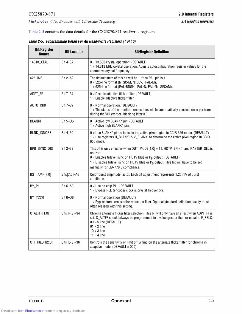
CX25870/871 2.0 Internal Registers
Flicker-Free Video Encoder with Ultrascale Technology 2.4 Reading Registers
100381B Conexant 2-9
Table 2-5 contains the data details for the CX25870/871 read/write registers.
Table 2-5. Programming Detail For All Read/Write Registers (1 of 16)
Bit/Register Names
Bit Location Bit/Register Definition
14318_XTAL Bit 4–3A 0 = 13.500 crystal operation. (DEFAULT)1 = 14.318 MHz crystal operation. Adjusts autoconfiguration register values for the
alternative crystal frequency.
625LINE Bit 2–A2 The default state of this bit will be 1 if the PAL pin is 1.0 = 525-line format (NTSC-M, NTSC-J, PAL-M).1 = 625-line format (PAL-BDGHI, PAL-N, PAL-Nc, SECAM).
ADPT_FF Bit 7–34 0 = Disable adaptive flicker filter. (DEFAULT)
1 = Enable adaptive flicker filter.
AUTO_CHK Bit 7–32 0 = Normal operation. (DEFAULT)1 = The status of the monitor connections will be automatically checked once per frame during the VBI (vertical blanking interval).
BLANKI Bit 5–D6 0 = Active low BLANK* pin. (DEFAULT)
1 = Active high BLANK* pin.
BLNK_IGNORE Bit 4–6C 0 = Use BLANK* pin to indicate the active pixel region in CCIR 656 mode. (DEFAULT)1 = Use registers H_BLANKI & V_BLANKI to determine the active pixel region in CCIR 656 mode.
BPB_SYNC_DIS Bit 3–2E This bit is only effective when OUT_MODE[1:0] = 11, HDTV_EN = 1, and RASTER_SEL is
nonzero.0 = Enables trilevel sync on HDTV Blue or PB output. (DEFAULT)
1 = Disables trilevel sync on HDTV Blue or PB output. This bit will have to be set
manually for EIA-770.3 compliance.
BST_AMP[7:0] Bits[7:0]–A6 Color burst amplitude factor. Each bit adjustment represents 1.25 mV of burst amplitude.
BY_PLL Bit 6–A0 0 = Use on chip PLL (DEFAULT)1 = Bypass PLL (encoder clock is crystal frequency).
BY_YCCR Bit 6–D8 0 = Normal operation (DEFAULT)
1 = Bypass luma cross color reduction filter. Optimal standard definition quality most often realized with this setting.
C_ALTFF[1:0] Bits [4:3]–34 Chroma alternate flicker filter selection. This bit will only have an effect when ADPT_FF is
set. C_ALTFF should always be programmed to a value greater than or equal to F_SELC.00 = 5 line (DEFAULT)01 = 2 line
10 = 3 line11 = 4 line
C_THRESH[2:0] Bits [5:3]–36 Controls the sensitivity or limit of turning on the alternate flicker filter for chroma in adaptive mode. (DEFAULT = 000)
Downloaded from Elcodis.com electronic components distributor

2.0 Internal Registers CX25870/871
2.4 Reading Registers Flicker-Free Video Encoder with Ultrascale Technology
2-10 Conexant 100381B
CATTENUATE[2:0] Bits [2:0]–CC Chroma Attenuation. Used for saturation control.
000 = 1.0 gain No Attenuation (DEFAULT)001 = 15/16 gain010 = 7/8 gain
011 = 3/4 gain100 = 1/2 gain101 = 1/4 gain
110 = 1/8 gain111 = 0 gain (Force Chroma to 0)
CC_ADD[11:0] Bits [3:0]–D4 and bits [7:0]–D2
Closed-captioning DTO increment.
CCF1B1[7:0] Bits [7:0]–C0 This is the first byte of closed-caption information for the odd field, line 21 for NTSC or
line 22 for PAL. Data is encoded LSB first.
CCF1B2[7:0] Bits [7:0]–C2 This is the second byte of closed-caption information for the odd field, line 21 for NTSC or line 22 for PAL. Data is encoded LSB first.
CCF2B1[7:0] Bits [7:0]–BC This is the first byte of closed-caption information for the even field, line 284 for NTSC or line 335 for PAL. Data is encoded LSB first.
CCF2B2[7:0] Bits [7:0]–BE This is the second byte of closed-caption information for the even field, line 284 for
NTSC or line 335 for PAL. Data is encoded LSB first.
CCORING[2:0] Bits [5:3]–CC Chroma Coring. Values below the CCORING[2:0] limit are automatically clamped to a saturation value of 0.
000 = Bypass (DEFAULT)
001 = 1/128 of range (± 1/256 of range)010 = 1/64 of range (± 1/128 of range)011 = 1/32 of range (± 1/64 of range)
100 = 1/16 of range (± 1/32 of range)101 = 1/8 of range (± 1/16 of range)110 = 1/4 of range (± 1/8 of range)
111 = Reserved
CCR_START[9]CCR_START[8]CCR_START[7:0]
Bit 7 of D6, bit 4 of D4, and bits [7:0] of D0
Closed-captioning clock run-in start in clock cycles from leading edge of HSYNC*.
CCSEL[3:0] Bits [3:0]–5E Line position of Closed Captioning (CC) Content.Controls which line Closed Captioning (CC) data is encoded. Each line enable is independent.
0001 = Closed Captioning (CC) on line 19 (525-line) and line 21 (625-line)0010 = Closed Captioning (CC) on line 20 (525-line) and line 22 (625-line)0100 = Closed Captioning (CC) on line 21 (525-line) and line 23 (625-line) (DEFAULT)
1000 = Closed Captioning (CC) on line 22 (525-line) and line 24 (625-line)
CHECK_STAT Bit 6–BA Writing a 1 to this bit checks the status of the monitor connections at the DAC output. This is also automatically performed on any reset condition, including a software reset. This bit must be cleared by the serial interface master.
CHROMA_BW Bit7–D8 0 = Normal chroma bandwidth. See Figure 1-28 (DEFAULT).
1 = Wide chroma bandwidth. See Figure 1-29.
Table 2-5. Programming Detail For All Read/Write Registers (2 of 16)
Bit/Register Names
Bit Location Bit/Register Definition
Downloaded from Elcodis.com electronic components distributor
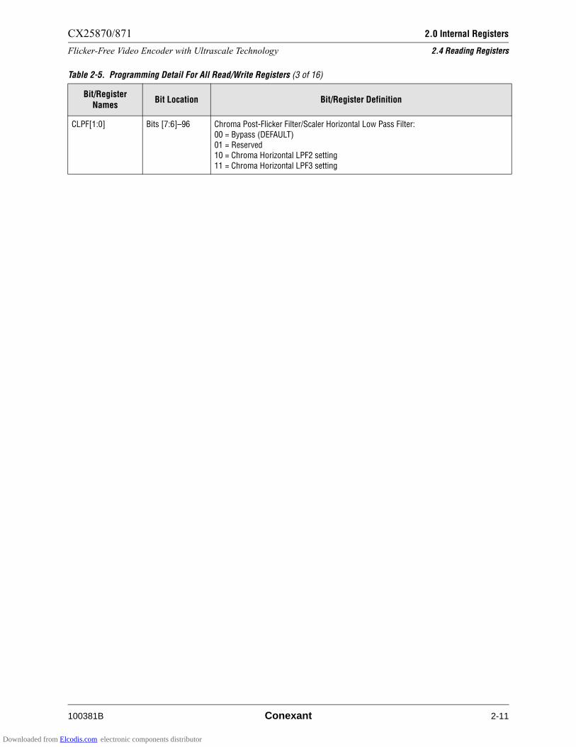
CX25870/871 2.0 Internal Registers
Flicker-Free Video Encoder with Ultrascale Technology 2.4 Reading Registers
100381B Conexant 2-11
CLPF[1:0] Bits [7:6]–96 Chroma Post-Flicker Filter/Scaler Horizontal Low Pass Filter:
00 = Bypass (DEFAULT)01 = Reserved10 = Chroma Horizontal LPF2 setting
11 = Chroma Horizontal LPF3 setting
Table 2-5. Programming Detail For All Read/Write Registers (3 of 16)
Bit/Register Names
Bit Location Bit/Register Definition
Downloaded from Elcodis.com electronic components distributor
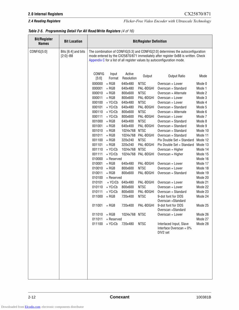
2.0 Internal Registers CX25870/871
2.4 Reading Registers Flicker-Free Video Encoder with Ultrascale Technology
2-12 Conexant 100381B
CONFIG[5:0] Bits [6:4] and bits
[2:0]–B8
The combination of CONFIG[5:3] and CONFIG[2:0] determines the autoconfiguration
mode entered by the CX25870/871 immediately after register 0xB8 is written. Check Appendix C for a list of all register values by autoconfiguration mode.
Table 2-5. Programming Detail For All Read/Write Registers (4 of 16)
Bit/Register Names
Bit Location Bit/Register Definition
CONFIG
[5:0]
Input
Format
Active
ResolutionOutput Output Ratio Mode
000000 = RGB 640x480 NTSC Overscan = Lower Mode 0
000001 = RGB 640x480 PAL-BDGHI Overscan = Standard Mode 1
000010 = RGB 800x600 NTSC Overscan = Alternate Mode 2
000011 = RGB 800x600 PAL-BDGHI Overscan = Lower Mode 3
000100 = YCrCb 640x480 NTSC Overscan = Lower Mode 4
000101 = YCrCb 640x480 PAL-BDGHI Overscan = Standard Mode 5
000110 = YCrCb 800x600 NTSC Overscan = Alternate Mode 6
000111 = YCrCb 800x600 PAL-BDGHI Overscan = Lower Mode 7
001000 = RGB 640x400 NTSC Overscan = Standard Mode 8
001001 = RGB 640x400 PAL-BDGHI Overscan = Standard Mode 9
001010 = RGB 1024x768 NTSC Overscan = Standard Mode 10
001011 = RGB 1024x768 PAL-BDGHI Overscan = Standard Mode 11
001100 = RGB 320x240 NTSC Pix Double Set = Standard Mode 12
001101 = RGB 320x240 PAL-BDGHI Pix Double Set = Standard Mode 13
001110 = YCrCb 1024x768 NTSC Overscan = Higher Mode 14
001111 = YCrCb 1024x768 PAL-BDGHI Overscan = Higher Mode 15
010000 = Reserved Mode 16
010001 = RGB 640x480 PAL-BDGHI Overscan = Lower Mode 17
010010 = RGB 800x600 NTSC Overscan = Lower Mode 18
010011 = RGB 800x600 PAL-BDGHI Overscan = Standard Mode 19
010100 = Reserved Mode 20
010101 = YCrCb 640x480 PAL-BDGHI Overscan = Lower Mode 21
010110 = YCrCb 800x600 NTSC Overscan = Lower Mode 22
010111 = YCrCb 800x600 PAL-BDGHI Overscan = Standard Mode 23
011000 = RGB 720x400 NTSC 9-dot font for DOS Overscan =Standard
Mode 24
011001 = RGB 720x400 PAL-BDGHI 9-dot font for DOS
Overscan =Standard
Mode 25
011010 = RGB 1024x768 NTSC Overscan = Lower Mode 26
011011 = Reserved Mode 27
011100 = YCrCb 720x480 NTSC Interlaced Input, Slave Interface Overscan = 0%
DIV2 set
Mode 28
Downloaded from Elcodis.com electronic components distributor

CX25870/871 2.0 Internal Registers
Flicker-Free Video Encoder with Ultrascale Technology 2.4 Reading Registers
100381B Conexant 2-13
CSC_SEL Bit 0–32 This bit is only effective when OUT_MODE[1:0] = 11, HDTV_EN = 1, and RASTER_SEL is
nonzero.0 = Standard color space conversion for RGB to Y (R-Y) (B-Y) based on
Y =0 .299R +0 .587G +0 .114 B (DEFAULT)1 = HDTV color space conversion for RGB to Y (R-Y) (B-Y) based onY = 0.2126R + 0.7152G + 0.0722B
CVBSD_INV Bit 2–D8 0 = Normal operation. (DEFAULT)
1 = Invert CVBS_DLY output.
DACDISA Bit 0–BA No more than 1 DAC should be disabled at any time.0 = Normal operation. (DEFAULT)1 = Disables DACA output. Current is set to 0 mA; output will go to 0 V.
DACDISB Bit 1–BA No more than 1 DAC should be disabled at any time.
0 = Normal operation. (DEFAULT)1 = Disables DACB output. Current is set to 0 mA; output will go to 0 V.
Table 2-5. Programming Detail For All Read/Write Registers (5 of 16)
Bit/Register Names
Bit Location Bit/Register Definition
011101 =YCrCb 720x576 PAL-BDGHI Interlaced Input, Slave Interface Overscan = 0%
DIV2 set
Mode 29
011110 = YCrCb 1024x768 NTSC Overscan = Lower Mode 30
011111 = Reserved Mode 31
100000 = RGB 640x480 NTSC Overscan = Higher Mode 32
100001 = RGB 640x480 PAL-BDGHI Overscan = Higher Mode 33
100010 = RGB 800x600 NTSC Overscan = Higher Mode 34
100011 = RGB 800x600 PAL-BDGHI Overscan = Higher Mode 35
100100 = YCrCb 640x480 NTSC Overscan = Higher Mode 36
100101 = YCrCb 640x480 PAL-BDGHI Overscan = Higher Mode 37
100110 = YCrCb 800x600 NTSC Overscan = Higher Mode 38
100111 = YCrCb 800x600 PAL-BDGHI Overscan = Higher Mode 39
101000 = RGB 800x600 NTSC Overscan = Standard Mode 40
101001 = RGB 320x200 PAL-BDGHI Pix Double Set Overscan = Standard
Mode 41
101010 = RGB 1024x768 NTSC Overscan = Higher Mode 42
101011 = RGB 1024x768 PAL-BDGHI Overscan = Higher Mode 43
101100 = RGB 720x480 NTSC Noninterlaced Input for DVD Overscan = Very Low
Mode 44
101101 = RGB 320x200 NTSC Pix Double Set Overscan =
Standard
Mode 45
101110 = RGB 640x480 PAL-M (Brazil)
Overscan = Standard Mode 46
101111 = RGB 640x480 PAL-Nc (Argentina)
Overscan = Standard Mode 47
Downloaded from Elcodis.com electronic components distributor

2.0 Internal Registers CX25870/871
2.4 Reading Registers Flicker-Free Video Encoder with Ultrascale Technology
2-14 Conexant 100381B
DACDISC Bit 2–BA No more than 1 DAC should be disabled at any time.
0 = Normal operation. (DEFAULT)1 = Disables DACC output. Current is set to 0 mA; output will go to 0 V.
DACDISD Bit 3–BA No more than 1 DAC should be disabled at any time.0 = Normal Operation. (DEFAULT)
1 = Disables DACD output. Current is set to 0 mA; output will go to 0 V.
DACOFF Bit 4–BA 0 = Normal operation. (DEFAULT)1 = Disables DAC output current and internal voltage reference for all DACs. This will limit power consumption to just the internal digital circuitry.
DATDLY Bit 7–74 0 = No delay in falling edge pixel data. (DEFAULT)
1 = Delays the falling edge pixel data by 1 full clock period. This bit is used to correct a multiplexed input data sequence that delivers a pixel on a falling edge and the following rising edge (rather than a rising edge and the following falling edge, as expected).
DATDLY_RE Bit 2–32 0 = No delay in rising edge pixel data. (DEFAULT)
1 = Delays the rising edge pixel data by 1 full clock period. This bit is used together with DATSWP to correct a multiplexed input data sequence that delivers a pixel on a falling edge and the following rising edge with the falling edge and rising edge data swapped.
DATSWP Bit 6–74 0 = VGA Encoder expects an order of rising edge data/falling edge data coming from the
graphics controller (DEFAULT).1 = Swaps the falling edge pixel data with the rising edge pixel data at the input of the pixel port.
DB_LIMITN[10:8
DB_LIMITN[7:0]
Bits [5:3]–54 and
bits [7:0]–52
Lower bound limit for DB frequency deviation in SECAM. Review SECAM Output Section.
DB_LIMITP[10:8DB_LIMITP[7:0]
Bits [2:0]–54 and bits [7:0]–50
Upper bound limit for DB frequency deviation in SECAM. Review SECAM Output Section.
DCHROMA Bit 1–C4 0 = Normal operation. (DEFAULT)1 = Disable the chrominance portion of video output. Composite and S-Video outputs
appear as gray scale.
DIS_CLKI Bit 3–30 0 = Normal operation. (DEFAULT)1 = Disable CLKI input.Disabling the CLKI input is separate from the sleep bit and SLEEP pin. This forces the
CX25870/871 to use an external clock as the clock source for the CX25870/871 or as the PLL input.
DIS_CLKO Bit 1–30 0 = Enable CLKO output. (DEFAULT)
1 = Three-state CLKO output.This will disable the CLKO output when not needed, i.e., an external clock is used (Slave Interface). Disabling CLKO is also effective in reducing the current draw in SLEEP mode.
DIS_FFILT Bit 6–C8 0 = Enables Standard Flicker Filter. (DEFAULT)
1 = Disables Standard Flicker Filter.
DIS_GMSHC Bit 6–CC 0 = Enables Chroma Pseudo Gamma Removal.1 = Disables Chroma Pseudo Gamma Removal. (DEFAULT)
DIS_GMSHY Bit 6–CA 0 = Enables Luma Pseudo Gamma Removal.1 = Disables Luma Pseudo Gamma Removal. (DEFAULT)
DIS_GMUSHC Bit 7–CC 0 = Enables Chroma Anti-Pseudo Gamma Removal.
1 = Disables Chroma Anti-Pseudo Gamma Removal. (DEFAULT)
Table 2-5. Programming Detail For All Read/Write Registers (6 of 16)
Bit/Register Names
Bit Location Bit/Register Definition
Downloaded from Elcodis.com electronic components distributor
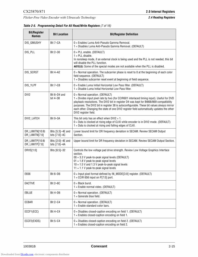
CX25870/871 2.0 Internal Registers
Flicker-Free Video Encoder with Ultrascale Technology 2.4 Reading Registers
100381B Conexant 2-15
DIS_GMUSHY Bit 7–CA 0 = Enables Luma Anti-Pseudo Gamma Removal.
1 = Disables Luma Anti-Pseudo Gamma Removal. (DEFAULT)
DIS_PLL Bit 2–30 0 = PLL enable. (DEFAULT)1 = PLL disable.In nonsleep mode, if an external clock is being used and the PLL is not needed, this bit
will disable the PLL function. NOTE(S): Some of the special modes are not available when the PLL is disabled.
DIS_SCRST Bit 4–A2 0 = Normal operation. The subcarrier phase is reset to 0 at the beginning of each color field sequence. (DEFAULT)
1 = Disables subcarrier reset event at beginning of field sequence.
DIS_YLPF Bit 7–C8 0 = Enable Luma Initial Horizontal Low Pass filter. (DEFAULT)1 = Disable Luma Initial Horizontal Low Pass filter.
DIV2 Bit 6–D4 andbit 4–38
0 = Normal operation. (DEFAULT)1 = Divides input pixel rate by two (for CCIR601 interlaced timing input). Useful for DVD
playback resolutions. The DIV2 bit in register D4 was kept for Bt868/869 compatibility purposes. The DIV2 bit in register 38 is autoconfigurable. These bit values always mirror each other. Changing the state of one DIV2 register field automatically updates the other
DIV2 register field.
DIV2_LATCH Bit 0–3A This bit only has an effect when DIV2 = 1.0 = Data is clocked at rising edge of CLKI while encoder is in DIV2 mode. (DEFAULT)1 = Data is clocked at rising and falling edges of CLKI.
DR_LIMITN[10:8
DR_LIMITN[7:0]
Bits [5:3]–4E and
bits [7:0]–4C
Lower bound limit for DR frequency deviation in SECAM. Review SECAM Output
Section.
DR_LIMITP[10:8DR_LIMITP[7:0]
Bits [2:0]–4E and bits [7:0]–4A
Upper bound limit for DR frequency deviation in SECAM. Review SECAM Output Section.
DRVS[1:0] Bits [6:5]–32 Controls the low voltage pad drive strength. Review Low Voltage Graphics Interface section.
00 = 3.3 V peak-to-peak signal levels (DEFAULT)01 = 1.8 V peak-to-peak signal levels10 = 1.5 V and 1.3 V peak-to-peak signal levels
11 = 1.1 V peak-to-peak signal levels
E656 Bit 6–D6 0 = Input pixel format defined by IN_MODE[3:0] register. (DEFAULT)1 = CCIR 656 input on P[7:0] port.
EACTIVE Bit 2–6C 0 = Black burst.
1 = Enable normal video. (DEFAULT)
EBLUE Bit 4–D6 0 = Normal operation. (DEFAULT)1 = Generate blue field.
ECBAR Bit 2–C4 0 = Normal operation. (DEFAULT)1 = Enable standard color bars.
ECCF1(ECC) Bit 4–C4 0 = Disables closed-caption encoding on field 1. (DEFAULT)
1 = Enables closed-caption encoding on field 1.
ECCF2(EXDS) Bit 5–C4 0 = Disables closed-caption encoding on field 2. (DEFAULT)1 = Enables closed-caption encoding on field 2.
Table 2-5. Programming Detail For All Read/Write Registers (7 of 16)
Bit/Register Names
Bit Location Bit/Register Definition
Downloaded from Elcodis.com electronic components distributor
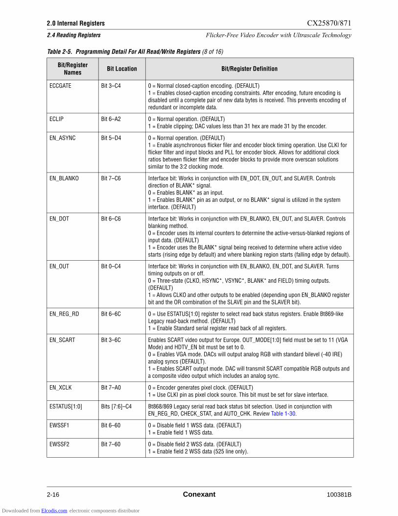
2.0 Internal Registers CX25870/871
2.4 Reading Registers Flicker-Free Video Encoder with Ultrascale Technology
2-16 Conexant 100381B
ECCGATE Bit 3–C4 0 = Normal closed-caption encoding. (DEFAULT)
1 = Enables closed-caption encoding constraints. After encoding, future encoding is disabled until a complete pair of new data bytes is received. This prevents encoding of redundant or incomplete data.
ECLIP Bit 6–A2 0 = Normal operation. (DEFAULT)
1 = Enable clipping; DAC values less than 31 hex are made 31 by the encoder.
EN_ASYNC Bit 5–D4 0 = Normal operation. (DEFAULT)1 = Enable asynchronous flicker filer and encoder block timing operation. Use CLKI for flicker filter and input blocks and PLL for encoder block. Allows for additional clock
ratios between flicker filter and encoder blocks to provide more overscan solutions similar to the 3:2 clocking mode.
EN_BLANKO Bit 7–C6 Interface bit: Works in conjunction with EN_DOT, EN_OUT, and SLAVER. Controls direction of BLANK* signal.
0 = Enables BLANK* as an input.1 = Enables BLANK* pin as an output, or no BLANK* signal is utilized in the system interface. (DEFAULT)
EN_DOT Bit 6–C6 Interface bit: Works in conjunction with EN_BLANKO, EN_OUT, and SLAVER. Controls
blanking method.0 = Encoder uses its internal counters to determine the active-versus-blanked regions of input data. (DEFAULT)
1 = Encoder uses the BLANK* signal being received to determine where active video starts (rising edge by default) and where blanking region starts (falling edge by default).
EN_OUT Bit 0–C4 Interface bit: Works in conjunction with EN_BLANKO, EN_DOT, and SLAVER. Turns timing outputs on or off.
0 = Three-state (CLKO, HSYNC*, VSYNC*, BLANK* and FIELD) timing outputs. (DEFAULT)1 = Allows CLKO and other outputs to be enabled (depending upon EN_BLANKO register
bit and the OR combination of the SLAVE pin and the SLAVER bit).
EN_REG_RD Bit 6–6C 0 = Use ESTATUS[1:0] register to select read back status registers. Enable Bt869-like Legacy read-back method. (DEFAULT)1 = Enable Standard serial register read back of all registers.
EN_SCART Bit 3–6C Enables SCART video output for Europe. OUT_MODE[1:0] field must be set to 11 (VGA
Mode) and HDTV_EN bit must be set to 0.0 = Enables VGA mode. DACs will output analog RGB with standard bilevel (-40 IRE)
analog syncs (DEFAULT).1 = Enables SCART output mode. DAC will transmit SCART compatible RGB outputs and a composite video output which includes an analog sync.
EN_XCLK Bit 7–A0 0 = Encoder generates pixel clock. (DEFAULT)
1 = Use CLKI pin as pixel clock source. This bit must be set for slave interface.
ESTATUS[1:0] Bits [7:6]–C4 Bt868/869 Legacy serial read back status bit selection. Used in conjunction with EN_REG_RD, CHECK_STAT, and AUTO_CHK. Review Table 1-30.
EWSSF1 Bit 6–60 0 = Disable field 1 WSS data. (DEFAULT)1 = Enable field 1 WSS data.
EWSSF2 Bit 7–60 0 = Disable field 2 WSS data. (DEFAULT)
1 = Enable field 2 WSS data (525 line only).
Table 2-5. Programming Detail For All Read/Write Registers (8 of 16)
Bit/Register Names
Bit Location Bit/Register Definition
Downloaded from Elcodis.com electronic components distributor

CX25870/871 2.0 Internal Registers
Flicker-Free Video Encoder with Ultrascale Technology 2.4 Reading Registers
100381B Conexant 2-17
F_SELC[2:0] Bits [5:3]–C8 Chroma Standard Flicker Filter:
000 = 5 Line (DEFAULT)001 = 2 Line010 = 3 Line
011 = 4 Line100 = Alternate 5 Line101 = Alternate 5 Line
110 = Alternate 5 Line111 = Alternate 5 Line
F_SELY[2:0] Bits [2:0]–C8 Luma Standard Flicker Filter:000 = 5 Line (DEFAULT)
001 = 2 Line 010 = 3 Line011 = 4 Line
100 = Alternate 5 Line101 = Alternate 5 Line110 = Alternate 5 Line
111 = Alternate 5 Line
FFCBAR Bit 5–6C 0 = Normal operation. (DEFAULT)1 = Enable flicker filtered color bars.
FFRTN Bit 7–36 Alternate flicker filter detect and select. This bit is effective only when ADPT_FF = 1.0 = Once the adaptive algorithm selects the alternate filter, use that filter’s coefficients for
the rest of the samples for that line. For example, the sequence could be STD/STD/ALT/ALT/ALT; (DEFAULT)1 = Once the adaptive algorithm selects the alternate filter, use the filter’s coefficients for
that sample only. For example, the sequence with FFRTN=1 could be STD/STD/ALT/STD/STD.
FIELD_ID Bit 3–D8 0 = Suppress the SECAM field synchronization signal. (DEFAULT)1 = Enable the SECAM field synchronization signal (bottle-neck pulses).
FIELDI Bit 5–C6 0 = Logical 1 from the FIELD pin indicates an even field. (DEFAULT)
1 = Logical 1 from the FIELD pin indicates an odd field.
FILFSCONV[5:0] Bits [5:0]–58 Adjust SECAM high frequency preemphasis filter according to the clock frequency.Review the SECAM Output section for the correct equations.
FIL4286INCR[7:0] Bits [7:0]–56 Adds a phase offset to the UV digital components.
Review the SECAM Output section for the correct equations.
FLD_MODE[1:0] Bits [1:0]–6C CX25870/871 uses this bit to interpret HSYNC* and VSYNC* edges and field detection in slave mode.00 = A leading edge of VSYNC* that occurs within &1/4 of HCLKI from the leading edge
of HSYNC* indicates the beginning of odd field. A leading edge of VSYNC* that occurs within &1/4 of HCLKI from the center of the line indicates the beginning of even field.01 = A leading edge of VSYNC* occurs during HSYNC* active indicates the beginning of
odd field. A leading edge of VSYNC* occurs during HSYNC* inactive indicates the beginning of even field. 10 = A leading edge of VSYNC* coincides with the leading edge of HSYNC* indicates the
beginning of odd field. A leading edge of VSYNC* does not coincide with the leading edge of HSYNC* indicated the beginning of even field. (DEFAULT)11 = Reserved.
Table 2-5. Programming Detail For All Read/Write Registers (9 of 16)
Bit/Register Names
Bit Location Bit/Register Definition
Downloaded from Elcodis.com electronic components distributor
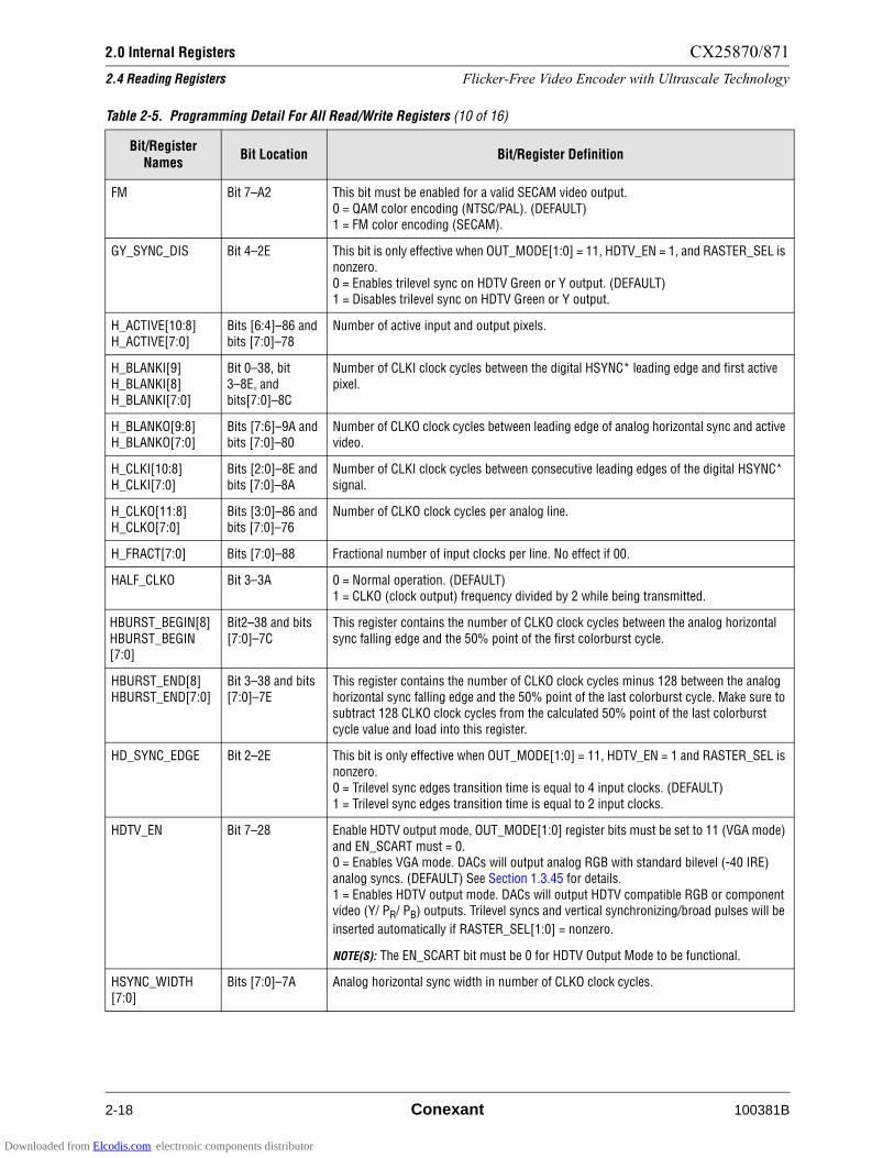
2.0 Internal Registers CX25870/871
2.4 Reading Registers Flicker-Free Video Encoder with Ultrascale Technology
2-18 Conexant 100381B
FM Bit 7–A2 This bit must be enabled for a valid SECAM video output.
0 = QAM color encoding (NTSC/PAL). (DEFAULT)1 = FM color encoding (SECAM).
GY_SYNC_DIS Bit 4–2E This bit is only effective when OUT_MODE[1:0] = 11, HDTV_EN = 1, and RASTER_SEL is nonzero.
0 = Enables trilevel sync on HDTV Green or Y output. (DEFAULT)1 = Disables trilevel sync on HDTV Green or Y output.
H_ACTIVE[10:8]H_ACTIVE[7:0]
Bits [6:4]–86 and bits [7:0]–78
Number of active input and output pixels.
H_BLANKI[9]
H_BLANKI[8]H_BLANKI[7:0]
Bit 0–38, bit
3–8E, and bits[7:0]–8C
Number of CLKI clock cycles between the digital HSYNC* leading edge and first active
pixel.
H_BLANKO[9:8]H_BLANKO[7:0]
Bits [7:6]–9A and bits [7:0]–80
Number of CLKO clock cycles between leading edge of analog horizontal sync and active video.
H_CLKI[10:8]
H_CLKI[7:0]
Bits [2:0]–8E and
bits [7:0]–8A
Number of CLKI clock cycles between consecutive leading edges of the digital HSYNC*
signal.
H_CLKO[11:8]H_CLKO[7:0]
Bits [3:0]–86 and bits [7:0]–76
Number of CLKO clock cycles per analog line.
H_FRACT[7:0] Bits [7:0]–88 Fractional number of input clocks per line. No effect if 00.
HALF_CLKO Bit 3–3A 0 = Normal operation. (DEFAULT)1 = CLKO (clock output) frequency divided by 2 while being transmitted.
HBURST_BEGIN[8]
HBURST_BEGIN [7:0]
Bit2–38 and bits
[7:0]–7C
This register contains the number of CLKO clock cycles between the analog horizontal
sync falling edge and the 50% point of the first colorburst cycle.
HBURST_END[8]HBURST_END[7:0]
Bit 3–38 and bits [7:0]–7E
This register contains the number of CLKO clock cycles minus 128 between the analog horizontal sync falling edge and the 50% point of the last colorburst cycle. Make sure to
subtract 128 CLKO clock cycles from the calculated 50% point of the last colorburst cycle value and load into this register.
HD_SYNC_EDGE Bit 2–2E This bit is only effective when OUT_MODE[1:0] = 11, HDTV_EN = 1 and RASTER_SEL is nonzero.
0 = Trilevel sync edges transition time is equal to 4 input clocks. (DEFAULT)1 = Trilevel sync edges transition time is equal to 2 input clocks.
HDTV_EN Bit 7–28 Enable HDTV output mode, OUT_MODE[1:0] register bits must be set to 11 (VGA mode)
and EN_SCART must = 0.0 = Enables VGA mode. DACs will output analog RGB with standard bilevel (-40 IRE) analog syncs. (DEFAULT) See Section 1.3.45 for details.
1 = Enables HDTV output mode. DACs will output HDTV compatible RGB or component video (Y/ PR/ PB) outputs. Trilevel syncs and vertical synchronizing/broad pulses will be
inserted automatically if RASTER_SEL[1:0] = nonzero.
NOTE(S): The EN_SCART bit must be 0 for HDTV Output Mode to be functional.
HSYNC_WIDTH [7:0]
Bits [7:0]–7A Analog horizontal sync width in number of CLKO clock cycles.
Table 2-5. Programming Detail For All Read/Write Registers (10 of 16)
Bit/Register Names
Bit Location Bit/Register Definition
Downloaded from Elcodis.com electronic components distributor
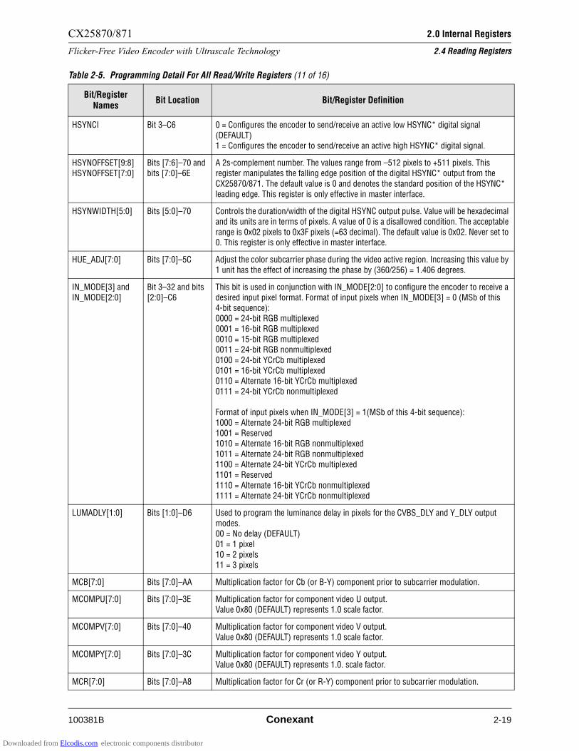
CX25870/871 2.0 Internal Registers
Flicker-Free Video Encoder with Ultrascale Technology 2.4 Reading Registers
100381B Conexant 2-19
HSYNCI Bit 3–C6 0 = Configures the encoder to send/receive an active low HSYNC* digital signal
(DEFAULT)1 = Configures the encoder to send/receive an active high HSYNC* digital signal.
HSYNOFFSET[9:8]HSYNOFFSET[7:0]
Bits [7:6]–70 and bits [7:0]–6E
A 2s-complement number. The values range from –512 pixels to +511 pixels. This register manipulates the falling edge position of the digital HSYNC* output from the
CX25870/871. The default value is 0 and denotes the standard position of the HSYNC* leading edge. This register is only effective in master interface.
HSYNWIDTH[5:0] Bits [5:0]–70 Controls the duration/width of the digital HSYNC output pulse. Value will be hexadecimal and its units are in terms of pixels. A value of 0 is a disallowed condition. The acceptable
range is 0x02 pixels to 0x3F pixels (=63 decimal). The default value is 0x02. Never set to 0. This register is only effective in master interface.
HUE_ADJ[7:0] Bits [7:0]–5C Adjust the color subcarrier phase during the video active region. Increasing this value by 1 unit has the effect of increasing the phase by (360/256) = 1.406 degrees.
IN_MODE[3] and
IN_MODE[2:0]
Bit 3–32 and bits
[2:0]–C6
This bit is used in conjunction with IN_MODE[2:0] to configure the encoder to receive a
desired input pixel format. Format of input pixels when IN_MODE[3] = 0 (MSb of this 4-bit sequence):0000 = 24-bit RGB multiplexed
0001 = 16-bit RGB multiplexed0010 = 15-bit RGB multiplexed0011 = 24-bit RGB nonmultiplexed
0100 = 24-bit YCrCb multiplexed0101 = 16-bit YCrCb multiplexed0110 = Alternate 16-bit YCrCb multiplexed
0111 = 24-bit YCrCb nonmultiplexed
Format of input pixels when IN_MODE[3] = 1(MSb of this 4-bit sequence):
1000 = Alternate 24-bit RGB multiplexed1001 = Reserved1010 = Alternate 16-bit RGB nonmultiplexed
1011 = Alternate 24-bit RGB nonmultiplexed1100 = Alternate 24-bit YCrCb multiplexed1101 = Reserved
1110 = Alternate 16-bit YCrCb nonmultiplexed1111 = Alternate 24-bit YCrCb nonmultiplexed
LUMADLY[1:0] Bits [1:0]–D6 Used to program the luminance delay in pixels for the CVBS_DLY and Y_DLY output
modes.00 = No delay (DEFAULT)01 = 1 pixel
10 = 2 pixels11 = 3 pixels
MCB[7:0] Bits [7:0]–AA Multiplication factor for Cb (or B-Y) component prior to subcarrier modulation.
MCOMPU[7:0] Bits [7:0]–3E Multiplication factor for component video U output.Value 0x80 (DEFAULT) represents 1.0 scale factor.
MCOMPV[7:0] Bits [7:0]–40 Multiplication factor for component video V output.
Value 0x80 (DEFAULT) represents 1.0 scale factor.
MCOMPY[7:0] Bits [7:0]–3C Multiplication factor for component video Y output.Value 0x80 (DEFAULT) represents 1.0. scale factor.
MCR[7:0] Bits [7:0]–A8 Multiplication factor for Cr (or R-Y) component prior to subcarrier modulation.
Table 2-5. Programming Detail For All Read/Write Registers (11 of 16)
Bit/Register Names
Bit Location Bit/Register Definition
Downloaded from Elcodis.com electronic components distributor

2.0 Internal Registers CX25870/871
2.4 Reading Registers Flicker-Free Video Encoder with Ultrascale Technology
2-20 Conexant 100381B
MODE2X Bit 7–D4 0 = Normal operation (DEFAULT).
1 = Divides selected input clock by two (allows for single edge rather than double-edge clock input for pixel latching).
MSC[31:0] Bits [7:0]–B4, B2, B0, AE
Subcarrier increment.
MSC_DB[31:0] Bits [7:0]–48,
-46, -44, -42
Subcarrier increment for Db component of SECAM.
MSC_DB = int ((272/H_CLKO) * 232 + 0.5)
MY[7:0] Bits [7:0]–AC Multiplication factor for Luma component. Controls adjustment of contrast.
NI_OUT Bit 0–A2 0 = Interlaced analog video output. (DEFAULT)1 = Noninterlaced analog video output.
OFFSET_RGB Bit 1–32 This bit is only effective when OUT_MODE[1:0] = 11, HDTV_EN = 1, and RASTER_SEL is nonzero.
0 = Standard RGB digital input. Range is 0 – 255 decimal. (DEFAULT)1 = HDTV OFFSET RGB digital input. Range is 16 – 235 decimal.
OUT_MODE[1:0] Bits [3:2]–D6 00 = Video[0] = Composite (CVBS), Video[1] = Luminance (Y), Video[2] = Chrominance (C), Video[3] = Luma_Delay (Y_DLY) (DEFAULT)
01 = Video[0-3] is CVBS_DLY/ Y/ C/ Y_DLY10 = Video[0-3] is V/ Y/ U/ Y_DLY11 = Video[0-3] is VGA (RGB/x), SCART, or HDTV output mode. See EN_SCART and
HDTV_EN bit descriptions for more programming detail.
OUT_MUXA[1:0] Bits [1:0]–CE 00 = Output Video[0] on DACA (DEFAULT = Composite (CVBS))01 = Output Video[1] on DACA10 = Output Video[2] on DACA
11 = Output Video[3] on DACA
OUT_MUXB[1:0] Bits [3:2]–CE 00 = Output Video[0] on DACB01 = Output Video[1] on DACB (DEFAULT = Luminance (Y)10 = Output Video[2] on DACB
11 = Output Video[3] on DACB
OUT_MUXC[1:0] Bits [5:4]–CE 00 = Output Video[0] on DACC01 = Output Video[1] on DACC10 = Output Video[2] on DACC (DEFAULT = Chrominance)
11 = Output Video[3] on DACC
OUT_MUXD[1:0] Bits [7:6]–CE 00 = Output Video[0] on DACD01 = Output Video[1] on DACD
10 = Output Video[2] on DACD11 = Output Video[3] on DACD (DEFAULT = Luma Delay (Y_DLY))
PAL_MD Bit 5–A2 Video output switch bit after power-up.0 = Disable phase alternation (NTSC and SECAM). (DEFAULT)
1 = Enable phase alternation (PAL).
NOTE(S): The PAL pin (#50) determines the power-up standard definition video output. This bit overrides the PAL pin after power-up.
PHASE_OFF[7:0] Bits [7:0]–B6 Subcarrier phase offset. Default value is 00. SCH Phase increased by 1.406 degrees per bit increment.
Table 2-5. Programming Detail For All Read/Write Registers (12 of 16)
Bit/Register Names
Bit Location Bit/Register Definition
Downloaded from Elcodis.com electronic components distributor
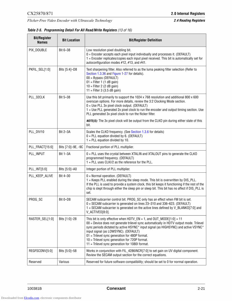
CX25870/871 2.0 Internal Registers
Flicker-Free Video Encoder with Ultrascale Technology 2.4 Reading Registers
100381B Conexant 2-21
PIX_DOUBLE Bit 6–38 Low resolution pixel doubling bit.
0 = Encoder accepts each pixel input individually and processes it. (DEFAULT)1 = Encoder replicates/copies each input pixel received. This bit is automatically set for autoconfiguration modes #12, #13, and #41.
PKFIL_SEL[1:0] Bits [5:4]–D8 Text sharpening filter. Also referred to as the luma peaking filter selection (Refer to
Section 1.3.36 and Figure 1-27 for details).00 = Bypass (DEFAULT)01 = Filter 1 (1 dB gain)
10 = Filter 2 (2 dB gain)11 = Filter 3 (3.5 dB gain)
PLL_32CLK Bit 5–38 Use this bit primarily to support the 1024 x 768 resolution and additional 800 x 600 overscan options. For more details, review the 3:2 Clocking Mode section.
0 = Use PLL 3x pixel clock output. (DEFAULT)1 = Use PLL generated 2x pixel clock to run the encoder and output timing section. Use PLL generated 3x pixel clock to run the flicker filter.
NOTE(S): The 3x pixel clock will be output from the CLKO pin during either state of this
bit.
PLL_DIV10 Bit 2–3A Scales the CLKO frequency. (See Section 1.3.6 for details)0 = PLL equation divided by 6. (DEFAULT)1 = PLL equation divided by 10.
PLL_FRACT[15:0] Bits [7:0]–9E, -9C Fractional portion of PLL multiplier.
PLL_INPUT Bit 1–3A 0 = PLL uses the crystal between XTALIN and XTALOUT pins to generate the CLKO
programmed frequency. (DEFAULT)1 = PLL uses CLKI/2 as the reference for the PLL.
PLL_INT[5:0] Bits [5:0]–A0 Integer portion of PLL multiplier.
PLL_KEEP_ALIVE Bit 4–30 0 = Normal operation. (DEFAULT)1 = Keeps PLL enabled during the sleep mode. This bit is overwritten by DIS_PLL.
If the PLL is used to provide a system clock, this bit keeps it functioning if the rest of the chip is slept through either the sleep pin or sleep bit. This bit has no affect if DIS_PLL is set.
PROG_SC Bit 0–D8 SECAM subcarrier control bit. PROG_SC only has an effect when FM bit is set.
0 = SECAM subcarrier is generated on lines 23–310 and 336–623. (DEFAULT)1 = SECAM subcarrier is generated on the active lines defined by V_BLANKO[7:0] and
V_ACTIVEO[8:0].
RASTER_SEL[1:0] Bits [1:0]–28 This bit is only effective when HDTV_EN = 1, and OUT_MODE[1:0] = 1100 = Device does not generate trilevel sync automatically in HDTV output mode. Trilevel sync periods dictated by active HSYNC* input signal (as HIGHSYNC) and active VSYNC*
input signal (as LOWSYNC). (DEFAULT)01 = Trilevel sync generation for 480P format.10 = Trilevel sync generation for 720P format.
11 = Trilevel sync generation for 1080I format.
REGFSCONV[5:0] Bits [5:0]–58 Works in conjunction with FIL_4286INCR[7:0] to set gain on UV digital component. Review the SECAM output section for the correct equations.
Reserved Various Reserved for future software compatibility; should be set to 0 for normal operation.
Table 2-5. Programming Detail For All Read/Write Registers (13 of 16)
Bit/Register Names
Bit Location Bit/Register Definition
Downloaded from Elcodis.com electronic components distributor
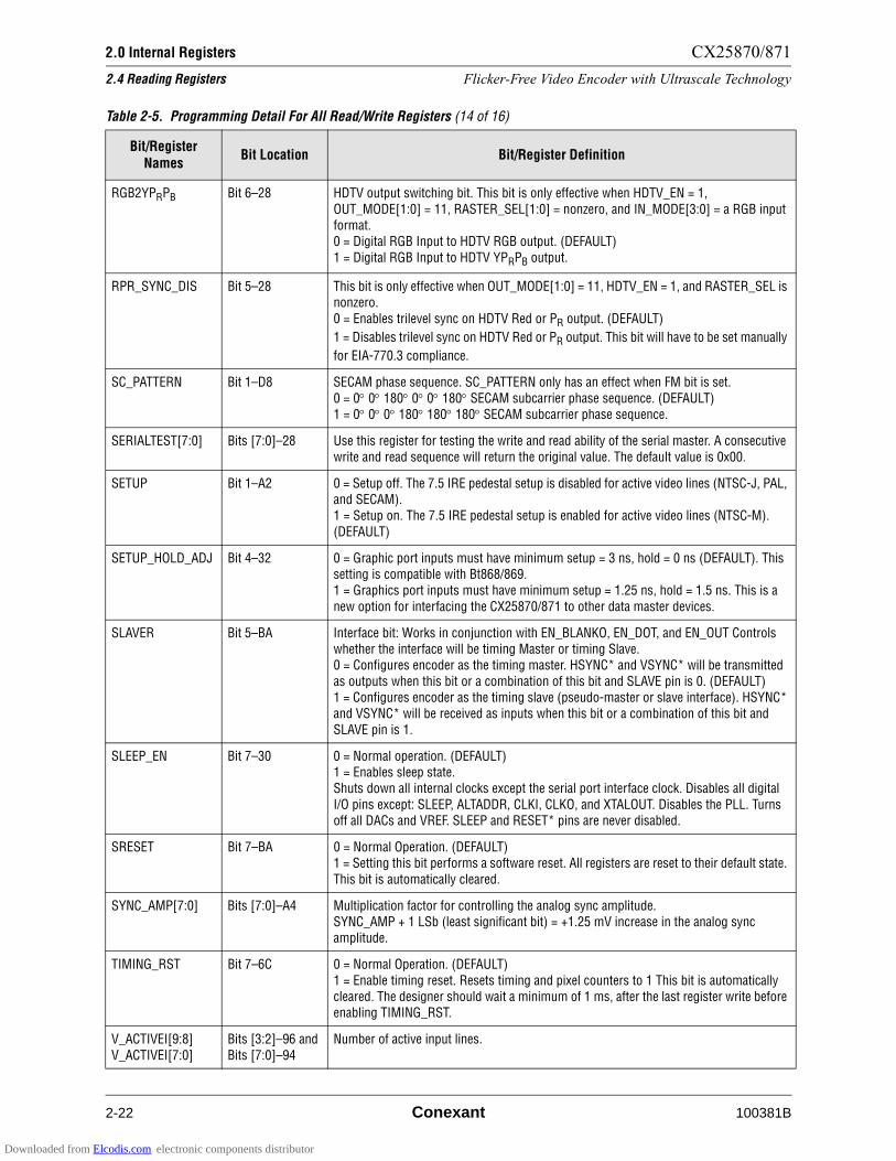
2.0 Internal Registers CX25870/871
2.4 Reading Registers Flicker-Free Video Encoder with Ultrascale Technology
2-22 Conexant 100381B
RGB2YPRPB Bit 6–28 HDTV output switching bit. This bit is only effective when HDTV_EN = 1,
OUT_MODE[1:0] = 11, RASTER_SEL[1:0] = nonzero, and IN_MODE[3:0] = a RGB input format.0 = Digital RGB Input to HDTV RGB output. (DEFAULT)
1 = Digital RGB Input to HDTV YPRPB output.
RPR_SYNC_DIS Bit 5–28 This bit is only effective when OUT_MODE[1:0] = 11, HDTV_EN = 1, and RASTER_SEL is nonzero.
0 = Enables trilevel sync on HDTV Red or PR output. (DEFAULT)
1 = Disables trilevel sync on HDTV Red or PR output. This bit will have to be set manually
for EIA-770.3 compliance.
SC_PATTERN Bit 1–D8 SECAM phase sequence. SC_PATTERN only has an effect when FM bit is set.
0 = 0' 0' 180' 0' 0' 180' SECAM subcarrier phase sequence. (DEFAULT)1 = 0' 0' 0' 180' 180' 180' SECAM subcarrier phase sequence.
SERIALTEST[7:0] Bits [7:0]–28 Use this register for testing the write and read ability of the serial master. A consecutive
write and read sequence will return the original value. The default value is 0x00.
SETUP Bit 1–A2 0 = Setup off. The 7.5 IRE pedestal setup is disabled for active video lines (NTSC-J, PAL, and SECAM).1 = Setup on. The 7.5 IRE pedestal setup is enabled for active video lines (NTSC-M).
(DEFAULT)
SETUP_HOLD_ADJ Bit 4–32 0 = Graphic port inputs must have minimum setup = 3 ns, hold = 0 ns (DEFAULT). This setting is compatible with Bt868/869.1 = Graphics port inputs must have minimum setup = 1.25 ns, hold = 1.5 ns. This is a
new option for interfacing the CX25870/871 to other data master devices.
SLAVER Bit 5–BA Interface bit: Works in conjunction with EN_BLANKO, EN_DOT, and EN_OUT Controls whether the interface will be timing Master or timing Slave.0 = Configures encoder as the timing master. HSYNC* and VSYNC* will be transmitted
as outputs when this bit or a combination of this bit and SLAVE pin is 0. (DEFAULT)1 = Configures encoder as the timing slave (pseudo-master or slave interface). HSYNC* and VSYNC* will be received as inputs when this bit or a combination of this bit and
SLAVE pin is 1.
SLEEP_EN Bit 7–30 0 = Normal operation. (DEFAULT)1 = Enables sleep state.Shuts down all internal clocks except the serial port interface clock. Disables all digital
I/O pins except: SLEEP, ALTADDR, CLKI, CLKO, and XTALOUT. Disables the PLL. Turns off all DACs and VREF. SLEEP and RESET* pins are never disabled.
SRESET Bit 7–BA 0 = Normal Operation. (DEFAULT)1 = Setting this bit performs a software reset. All registers are reset to their default state.
This bit is automatically cleared.
SYNC_AMP[7:0] Bits [7:0]–A4 Multiplication factor for controlling the analog sync amplitude.SYNC_AMP + 1 LSb (least significant bit) = +1.25 mV increase in the analog sync amplitude.
TIMING_RST Bit 7–6C 0 = Normal Operation. (DEFAULT)
1 = Enable timing reset. Resets timing and pixel counters to 1 This bit is automatically cleared. The designer should wait a minimum of 1 ms, after the last register write before enabling TIMING_RST.
V_ACTIVEI[9:8]
V_ACTIVEI[7:0]
Bits [3:2]–96 and
Bits [7:0]–94
Number of active input lines.
Table 2-5. Programming Detail For All Read/Write Registers (14 of 16)
Bit/Register Names
Bit Location Bit/Register Definition
Downloaded from Elcodis.com electronic components distributor
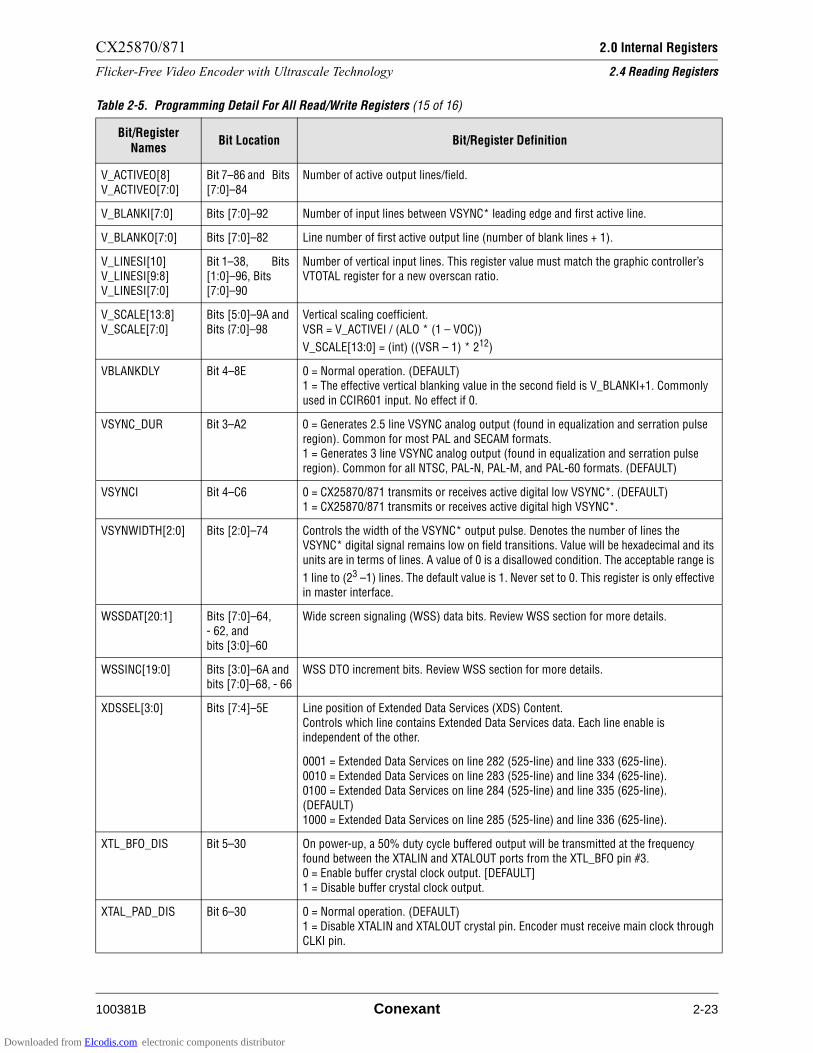
CX25870/871 2.0 Internal Registers
Flicker-Free Video Encoder with Ultrascale Technology 2.4 Reading Registers
100381B Conexant 2-23
V_ACTIVEO[8]
V_ACTIVEO[7:0]
Bit 7–86 and Bits
[7:0]–84
Number of active output lines/field.
V_BLANKI[7:0] Bits [7:0]–92 Number of input lines between VSYNC* leading edge and first active line.
V_BLANKO[7:0] Bits [7:0]–82 Line number of first active output line (number of blank lines + 1).
V_LINESI[10]V_LINESI[9:8]V_LINESI[7:0]
Bit 1–38, Bits [1:0]–96, Bits [7:0]–90
Number of vertical input lines. This register value must match the graphic controller’s VTOTAL register for a new overscan ratio.
V_SCALE[13:8]
V_SCALE[7:0]
Bits [5:0]–9A and
Bits 7:0]–98
Vertical scaling coefficient.
VSR = V_ACTIVEI / (ALO * (1 – VOC))
V_SCALE[13:0] = (int) ((VSR – 1) * 212)
VBLANKDLY Bit 4–8E 0 = Normal operation. (DEFAULT)1 = The effective vertical blanking value in the second field is V_BLANKI+1. Commonly
used in CCIR601 input. No effect if 0.
VSYNC_DUR Bit 3–A2 0 = Generates 2.5 line VSYNC analog output (found in equalization and serration pulse region). Common for most PAL and SECAM formats.1 = Generates 3 line VSYNC analog output (found in equalization and serration pulse
region). Common for all NTSC, PAL-N, PAL-M, and PAL-60 formats. (DEFAULT)
VSYNCI Bit 4–C6 0 = CX25870/871 transmits or receives active digital low VSYNC*. (DEFAULT)1 = CX25870/871 transmits or receives active digital high VSYNC*.
VSYNWIDTH[2:0] Bits [2:0]–74 Controls the width of the VSYNC* output pulse. Denotes the number of lines the VSYNC* digital signal remains low on field transitions. Value will be hexadecimal and its
units are in terms of lines. A value of 0 is a disallowed condition. The acceptable range is
1 line to (23 –1) lines. The default value is 1. Never set to 0. This register is only effective in master interface.
WSSDAT[20:1] Bits [7:0]–64,
- 62, and bits [3:0]–60
Wide screen signaling (WSS) data bits. Review WSS section for more details.
WSSINC[19:0] Bits [3:0]–6A and bits [7:0]–68, - 66
WSS DTO increment bits. Review WSS section for more details.
XDSSEL[3:0] Bits [7:4]–5E Line position of Extended Data Services (XDS) Content.
Controls which line contains Extended Data Services data. Each line enable is independent of the other.
0001 = Extended Data Services on line 282 (525-line) and line 333 (625-line).
0010 = Extended Data Services on line 283 (525-line) and line 334 (625-line).0100 = Extended Data Services on line 284 (525-line) and line 335 (625-line). (DEFAULT)
1000 = Extended Data Services on line 285 (525-line) and line 336 (625-line).
XTL_BFO_DIS Bit 5–30 On power-up, a 50% duty cycle buffered output will be transmitted at the frequency found between the XTALIN and XTALOUT ports from the XTL_BFO pin #3. 0 = Enable buffer crystal clock output. [DEFAULT]
1 = Disable buffer crystal clock output.
XTAL_PAD_DIS Bit 6–30 0 = Normal operation. (DEFAULT)1 = Disable XTALIN and XTALOUT crystal pin. Encoder must receive main clock through CLKI pin.
Table 2-5. Programming Detail For All Read/Write Registers (15 of 16)
Bit/Register Names
Bit Location Bit/Register Definition
Downloaded from Elcodis.com electronic components distributor
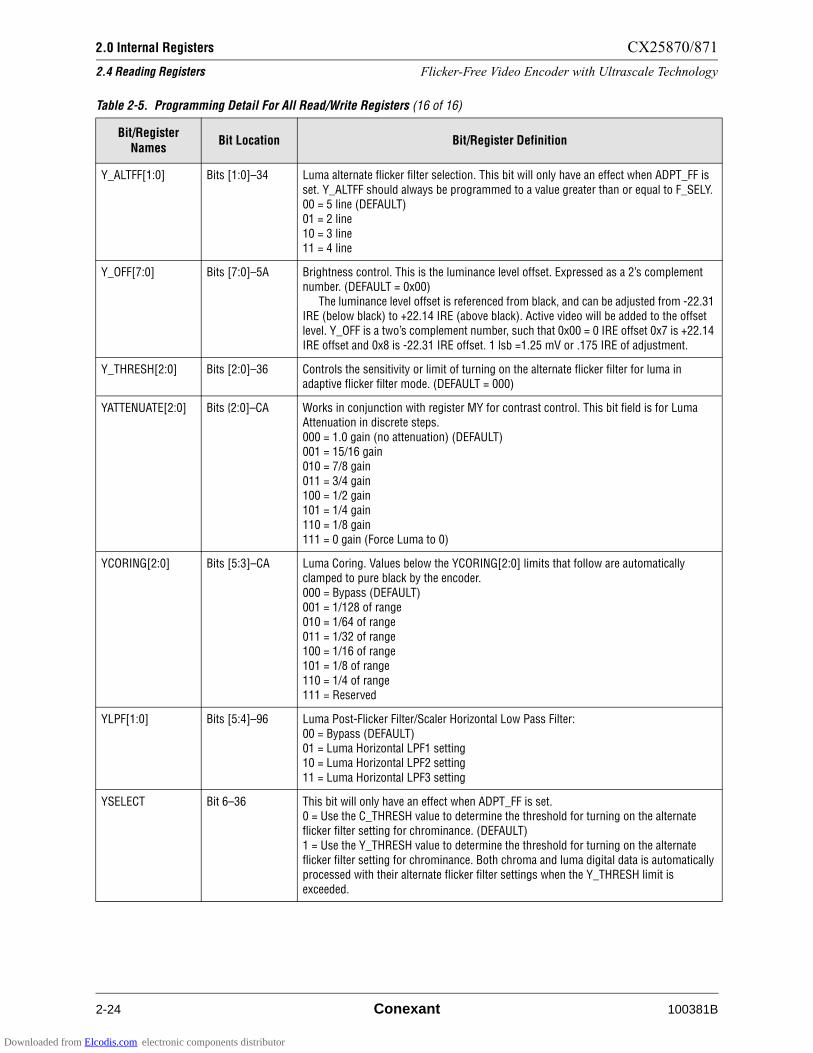
2.0 Internal Registers CX25870/871
2.4 Reading Registers Flicker-Free Video Encoder with Ultrascale Technology
2-24 Conexant 100381B
Y_ALTFF[1:0] Bits [1:0]–34 Luma alternate flicker filter selection. This bit will only have an effect when ADPT_FF is
set. Y_ALTFF should always be programmed to a value greater than or equal to F_SELY.00 = 5 line (DEFAULT)01 = 2 line
10 = 3 line11 = 4 line
Y_OFF[7:0] Bits [7:0]–5A Brightness control. This is the luminance level offset. Expressed as a 2’s complement number. (DEFAULT = 0x00)
The luminance level offset is referenced from black, and can be adjusted from -22.31 IRE (below black) to +22.14 IRE (above black). Active video will be added to the offset level. Y_OFF is a two’s complement number, such that 0x00 = 0 IRE offset 0x7 is +22.14
IRE offset and 0x8 is -22.31 IRE offset. 1 lsb =1.25 mV or .175 IRE of adjustment.
Y_THRESH[2:0] Bits [2:0]–36 Controls the sensitivity or limit of turning on the alternate flicker filter for luma in adaptive flicker filter mode. (DEFAULT = 000)
YATTENUATE[2:0] Bits 2:0]–CA Works in conjunction with register MY for contrast control. This bit field is for Luma Attenuation in discrete steps.
000 = 1.0 gain (no attenuation) (DEFAULT)001 = 15/16 gain010 = 7/8 gain
011 = 3/4 gain100 = 1/2 gain101 = 1/4 gain
110 = 1/8 gain111 = 0 gain (Force Luma to 0)
YCORING[2:0] Bits [5:3]–CA Luma Coring. Values below the YCORING[2:0] limits that follow are automatically clamped to pure black by the encoder.
000 = Bypass (DEFAULT)001 = 1/128 of range010 = 1/64 of range
011 = 1/32 of range100 = 1/16 of range101 = 1/8 of range
110 = 1/4 of range111 = Reserved
YLPF[1:0] Bits [5:4]–96 Luma Post-Flicker Filter/Scaler Horizontal Low Pass Filter:
00 = Bypass (DEFAULT)01 = Luma Horizontal LPF1 setting10 = Luma Horizontal LPF2 setting
11 = Luma Horizontal LPF3 setting
YSELECT Bit 6–36 This bit will only have an effect when ADPT_FF is set.0 = Use the C_THRESH value to determine the threshold for turning on the alternate flicker filter setting for chrominance. (DEFAULT)
1 = Use the Y_THRESH value to determine the threshold for turning on the alternate flicker filter setting for chrominance. Both chroma and luma digital data is automatically processed with their alternate flicker filter settings when the Y_THRESH limit is
exceeded.
Table 2-5. Programming Detail For All Read/Write Registers (16 of 16)
Bit/Register Names
Bit Location Bit/Register Definition
Downloaded from Elcodis.com electronic components distributor
100381B Conexant 3-1
3
3.0 PC Board Considerations
For optimum performance of the CX25870/871, proper CMOS layout techniques
should be studied before PC board layout is begun.
The layout should be optimized for lowest noise on the power and ground
planes by providing good decoupling. The trace length between groups of VAA
(or VDD) and GND (or VSS) pins should be as short as possible to minimize
inductive ringing.
A well-designed power distribution network is critical to eliminating digital
switching noise. The ground plane must provide a low-impedance return path for
the digital circuits. A PC board with a minimum of four layers is recommended,
with layers 1 (top) and 4 (bottom) for signals, and layers 2 and 3 for ground and
power, respectively.
3.1 Component Placement
Components should be placed as close as possible to the associated pin in order
for traces to be connected point to point. The optimum layout places the
CX25870/871 as close as possible to the power supply connector and the video
output connector, as illustrated in Figure 3-1.
Some other PC board layout tips to follow are:
• Include a silk screen layer of labels in your layout artwork showing each
component and its reference designation. Label numbered test nodes and
the correct polarity of diodes and electrolytic capacitors.
• Leave adequate space around components so ESD transients only have
minimally adverse effects on ICs.
• Make sure signals that need access for troubleshooting or analysis are easy
to find and probe.
Downloaded from Elcodis.com electronic components distributor
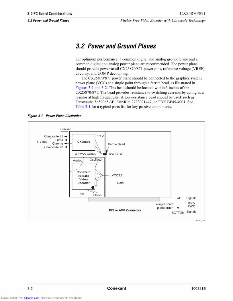
3.0 PC Board Considerations CX25870/871
3.2 Power and Ground Planes Flicker-Free Video Encoder with Ultrascale Technology
3-2 Conexant 100381B
3.2 Power and Ground Planes
For optimum performance, a common digital and analog ground plane and a
common digital and analog power plane are recommended. The power plane
should provide power to all CX25870/871 power pins, reference voltage (VREF)
circuitry, and COMP decoupling.
The CX25870/871 power plane should be connected to the graphics system
power plane (VCC) at a single point through a ferrite bead, as illustrated in
Figures 3-1 and 3-2. This bead should be located within 3 inches of the
CX25870/871. The bead provides resistance to switching currents by acting as a
resistor at high frequencies. A low-resistance bead should be used, such as
Ferroxcube 5659065-3B, Fair-Rite 2723021447, or TDK BF45-4001. See
Table 3-1 for a typical parts list for key passive components.
Figure 3-1. Power Plane Illustration
CX25870
Conexant(Bt835)Video
Decoder
Analog Oscillator
3.3 VAA-CX870
o VCC3.3
Ferrite Bead
Clocks5V
3.3 V
o VCC3.3
Data
PCI or AGP Connector
Bracket
Composite #1Luma
ChromeComposite #2
S-Video
4 layer boardplane order:
Signals
GNDPWR
SignalsBOTTOM
TOP
100381_017
Downloaded from Elcodis.com electronic components distributor

CX25870/871 3.0 PC Board Considerations
Flicker-Free Video Encoder with Ultrascale Technology 3.2 Power and Ground Planes
100381B Conexant 3-3
Figure 3-2. Connection Diagram for Output Filters and Other Key Passive Components/Standard Definition TV Out Only
100381_018a
Note(s):(1) VDDL VDD_CO, VDD_VREF must be tied to 3.3 V CX25870/871 Power Plane unless interface to low power graphics controller is required.(2) Depending on the parasitic capacitance of your PCB and loading expectations of your crystals, these capacitor values
may change slightly. Generally, the 27 pF and 33 pF combination matches a 20 pF internal XTAL load.(3) No RF Modulator has been included on any of the DAC outputs. Baseband video is always generated by the CX25870.
VAA
XTALIN
13.500 MHz XTAL
XTALOUT
COMPVBIAS
VDDL(1)
VDD_CO(1)
VDD_VREF(1)
VREF
GND
C7
C8
C2–C6
FSADJUST
+1.1 V to+1.8 V
RSET =75 Ω,1%
DACA
DACB
CX25870/871 Power Plane
To VideoConnector
Ground(Power SupplyConnector)
+3.3 V (VCC)
VAA
Schottky Diodes
Schottky DiodesSD LPF
CX25870/871
C10+
C1
FB
SD LPF
SD LPF
SD LPF
22 pF, 5%
1.8 µH, 5%
270 pF, 5% 330 pF,5%
GND
To FilterDAC Output
27 pF(2),5%
33 pF(2),5%
75 Ω,1%
75 Ω,1%
75 Ω,1%
75 Ω,1%
10KΩ1%
10KΩ1%
C9
P
P
DACC
DACD
P
P
P :
SD LPF
Downloaded from Elcodis.com electronic components distributor

3.0 PC Board Considerations CX25870/871
3.2 Power and Ground Planes Flicker-Free Video Encoder with Ultrascale Technology
3-4 Conexant 100381B
Figure 3-3. Connection Diagram for Output Filters and Other Key Passive Components/Standard and HDTV Out
100381_084
CX25870/871
DAC DCVBS = Composite #2
VAA3.3 V
123
1
2
3
D9BAT54SSOT-23
5443R10-004
R1175.0 "08051%
SD Filter
HD Filter
HD Filter
HD Filter
C21270 pF08055%
22 pF08055%
C22330 pF08055%
L11.8 µH12105%
DAC B Y = Lumaor HD Y
VAA3.3 V
123
1
2
3
D7BAT54SSOT-23
5443R10-004
R275.0 "08051%
C962 pF08055%
C833 pF08055%
C1075 pF08055%
BOUT
L10.27 µH
12105%
DAC C C = Chromaor HD PR
VAA3.3 V
123
1
2
3
D8BAT54SSOT-23
5443R10-004
R775.0 "08051%
C962 pF08055%
C833 pF08055%
C1075 pF08055%
COUT
L10.27 µH
12105%
DAC A CVBS = Composite #1or HD PB
VAA3.3 V
123
1
2
3
D9BAT54SSOT-23
5443R10-004
R1175.0 "08051%
C962 pF08055%
C833 pF08055%
C1075 pF08055%
DOUT
L10.27 µH
12105%
NOTE(S):1. HD Filter imparts a passband of DC to 30 MHz.2. SD Filter imparts a passband of DC to 8 MHz.
Downloaded from Elcodis.com electronic components distributor
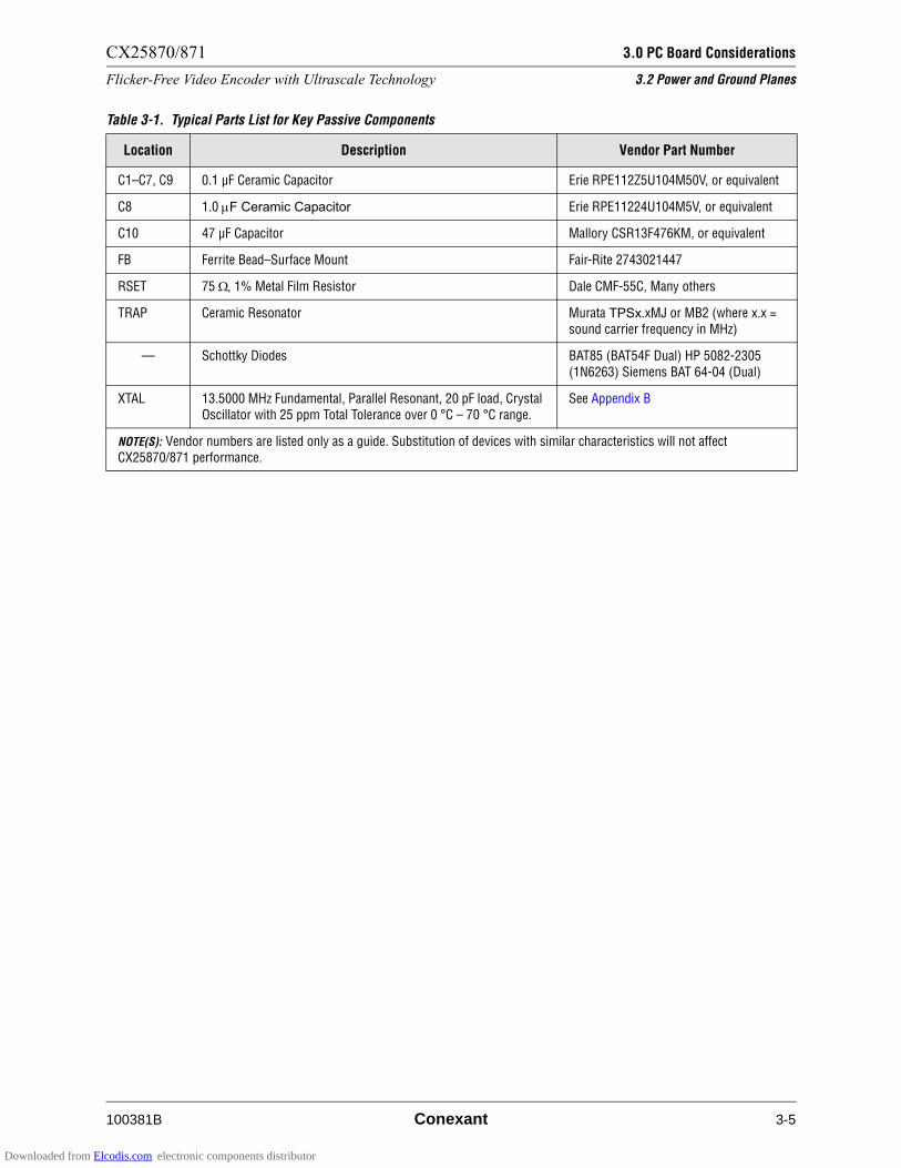
CX25870/871 3.0 PC Board Considerations
Flicker-Free Video Encoder with Ultrascale Technology 3.2 Power and Ground Planes
100381B Conexant 3-5
Table 3-1. Typical Parts List for Key Passive Components
Location Description Vendor Part Number
C1–C7, C9 0.1 µF Ceramic Capacitor Erie RPE112Z5U104M50V, or equivalent
C8 1.0 !F Ceramic Capacitor Erie RPE11224U104M5V, or equivalent
C10 47 µF Capacitor Mallory CSR13F476KM, or equivalent
FB Ferrite Bead–Surface Mount Fair-Rite 2743021447
RSET 75 ", 1% Metal Film Resistor Dale CMF-55C, Many others
TRAP Ceramic Resonator Murata TPSx.xMJ or MB2 (where x.x = sound carrier frequency in MHz)
— Schottky Diodes BAT85 (BAT54F Dual) HP 5082-2305
(1N6263) Siemens BAT 64-04 (Dual)
XTAL 13.5000 MHz Fundamental, Parallel Resonant, 20 pF load, Crystal Oscillator with 25 ppm Total Tolerance over 0 °C – 70 °C range.
See Appendix B
NOTE(S): Vendor numbers are listed only as a guide. Substitution of devices with similar characteristics will not affect CX25870/871 performance.
Downloaded from Elcodis.com electronic components distributor

3.0 PC Board Considerations CX25870/871
3.2 Power and Ground Planes Flicker-Free Video Encoder with Ultrascale Technology
3-6 Conexant 100381B
L1 1.8u
H
1210 5%
J4 RC
A J
AC
K2
2
1
3
C20
1.0
uF08
05
D2
DA
204K
SO
T-2
3
2
3
1
10K
OH
M08
05
R9
L4 1.8u
H
1210 5%
C19
22 p
F
0805
5%
J1 RC
A J
AC
K2
2
1
3
C21
270
pF
0805
5%
R11
75.0
OH
M
0805
1%
C22
330
pF
0805
5%
C8
22 p
F
0805
5%
C9
270
pF
0805
5%
D3
DA
204K
SO
T-2
3
2
3
1
10K
0805
R3
10K
0805
R4
10K
0805
R5
J2 RC
A J
AC
K2
2
1
3
10K
OH
M08
05
R6
D4
DA
204K
SO
T-2
3
2
3
1
J3 RC
A J
AC
K2
2
1
3
75 O
HM
, 1%
0805
1%R8
Y1
13.5
00 M
Hz
HC
49U
D1
DA
204K
SO
T-2
3
2
3
1
C23
27 p
F
0805
C24
33 p
F
0805
R1
75.0
OH
M
0805
1%
R12
33 O
HM
0805
C10
330
pF
0805
5%
L2 1.8u
H
1210 5%
C12
22 p
F
0805
5%
L3 1.8u
H
1210 5%
R14
33 O
HM
0805
C13
270
pF
0805
5%
C15
22 p
F
0805
5%
C16
270
pF
0805
5%
C1
10 u
F
7343
+
R2
75.0
OH
M
0805
1%
C14
330
pF
0805
5%
R7
75.0
OH
M
0805
1%
FB
1
FE
RR
ITE
BE
AD
Fai
r-R
ite
C17
330
pF
0805
5%
C11
0.1
uF08
05
VA
A_D
AC
A69
FIE
LD37
VA
A_D
AC
C73
XT
ALI
N63
XT
ALO
UT
62
VS
S3
22V
SS
221
VD
D1
VA
A_D
AC
B71
VS
S5
41
VS
S1
4
RE
SE
T*
53
BLA
NK
*38
VS
YN
C*
36H
SY
NC
*35
PA
L50
SLA
VE
51S
LEE
P52
ALT
AD
DR
48
VS
S4
31
SIC
(S
CL)
45
SID
(S
DA
)44
CLK
I54
CLK
O56
VR
EF
76
VB
IAS
77
FS
AD
JUS
T78
DA
CC
72
DA
CB
70
DA
CA
68
CO
MP
75
VA
A_P
LL59
VA
A_D
AC
D67
DA
CD
66
XT
L_B
FO
3
VS
S_S
I42
P[1
5]24
P[1
4]23
P[1
3]18
P[1
2]17
P[1
1]16
P[1
0]15
P[9
]14
P[8
]13
P[7
]12
P[6
]11
P[5
]10
P[4
]9
P[3
]8
P[2
]7
P[1
]6
P[0
]5
P[1
6]25
P[1
7]26
P[1
8]27
P[1
9]28
P[2
0]29
P[2
1]32
P[2
2]33
P[2
3]34
VS
S_S
O43
VD
D_S
O46
VD
D_S
I47
VD
D_V
RE
F49
VS
S_C
O55
VD
D_C
O57
AG
ND
_PLL
58
VD
D5
60
VD
D_X
61
VS
S_X
64
AG
ND
_DA
C65
AG
ND
_DA
C74
AG
ND
79
VA
A_V
RE
F80
VD
DL
40
VD
D3
20V
DD
219
VD
D1
2
VD
D4
30
VS
S/T
ES
T39
CX
2587
0/87
1
FIN
AL
PIN
OU
T 1
/02/
01
80 P
QF
P
10K
OH
M08
05
R10
C3
0.1
uF08
05
C4
0.1
uF08
05
C5
0.1
uF08
05
C6
0.1
uF08
05
C7
1.0
uF08
05
C2
0.01
uF
0805
P1
Con
nect
or
1 2 3 4
5
6
7
1
4
2
3
C18
0.1
uF08
05
RN
3A33
OH
M16
321
8
RN
3C3
6
RN
3D4
5
RN
3B2
7
RN
2C3
6
RN
2D4
5
RN
2B2
7
R15
33 O
HM
0805
RN
1C3
6
RN
1D4
5
RN
1B2
7
RN
2A33
OH
M16
321
8
RN
1A33
OH
M16
321
8
SW
DIP
-4
1 2 3 4
8 7 6 5
CB
LAN
K
VS
YN
C
HS
YN
C
CLK
IN
3V_S
CL
RE
SE
T
AO
UT
CLK
OU
T
3V_S
DA
DA
C_D
BO
UT
CO
UT
CO
UT
BO
UT
DO
UT
CR
YS
TA
L_O
UT
PU
T
DA
C_C
DA
C_B
I2C
_AD
DR
PA
L_C
TL
SLA
VE
_CT
L
SLE
EP
DA
C_A
FIE
LD
RSET RESISTOR
P2
P4
P9
P10
P6
P1
P3
P11
P5
P0
P7
P8
CX
2587
0_3.
3V
VA
A_3
.3V
VC
C_3
.3V
VA
A_3
.3V
VA
A_3
.3V
VA
A_3
.3V
CX
2587
0_3.
3V
CX
2587
0_3.
3V
CX
2587
0_3.
3V
CX
2587
0_3.
3V
CX
2587
0_3.
3V
HS
YN
C_B
I
VS
YN
C_B
I
CB
LAN
K_B
I
870_
CLK
IN
3V_S
DA
3V_S
CL RE
SE
T
870F
IELD
_OU
T
870C
LK_O
UT
P_I
N7
P_I
N3
P_I
N0
P_I
N2
P_I
N1
P_I
N4
P_I
N6
P_I
N5
P_I
N11
P_I
N8
P_I
N10
P_I
N9
XT
AL_
CLK
_Out
put
**24
bit R
GB
mul
tiple
xed
inte
rfac
e sh
own
in d
iagr
am
3.3V
AN
ALO
G S
UP
PLY
AN
D D
EC
OU
PLI
NG
2743
0214
47
If V
DD
_VR
EF
= 3
.3V
, the
n th
e fo
llow
ing
CX
2587
0/87
1 in
puts
mus
t
be r
ecei
ved
at 3
.3V
leve
ls:
CLK
I, H
SY
NC
*, V
SY
NC
*, B
LAN
K*,
and
the
pixe
l inp
uts-
P[0
] - P
[11]
PA
L
MA
ST
ER
AD
DR
x88
SLE
EP
PA
L
NO
RM
AL
AD
DR
x8A
SLA
VE
ALT
AD
DR
ST
AT
E IF
P
IN#=
0S
LEE
P
ST
AT
E IF
P
IN#=
1
CX
2587
0
PIN
#:
SLA
VE
NT
SC
see
char
t
5% 5%
**F
loat
XT
L_B
FO
if n
ot u
sed
C =
CH
RO
MA
(SC
AR
T =
B)
CV
BS
=C
ompo
site
(SC
AR
T =
R)
Y =
LU
MA
(SC
AR
T =
G)
**T
he ty
pe a
nd lo
catio
n of
eac
h
V
ideo
Out
put i
s se
lect
able
**R
esis
tor
pack
s M
US
T b
e pl
aced
as
clos
e as
pos
sibl
e to
gra
phic
s co
ntro
ller=
sour
ce
10%
**S
erie
s te
rmin
atio
n M
US
T b
e pl
aced
as
clo
se a
s po
ssib
le to
sou
rce=
enco
der
**R
14 M
US
T b
e pl
aced
as
clos
e as
pos
sibl
e to
sou
rce=
enco
der
S-V
ideo
Y/C
Out
put
If V
DD
_CO
& V
DD
L =
3.3
V, t
hen
the
follo
win
g C
X25
870/
871
outp
uts
will
be
tran
smitt
ed a
t 3.3
V le
vels
as
wel
l: C
LKO
, HS
YN
C*,
VS
YN
C*,
BLA
NK
*,
and
FIE
LD.
All
othe
r si
gnal
s w
ill a
lso
be a
t 3.3
V C
MO
S le
vels
unl
ess
deno
ted
othe
rwis
e.
Key
Cry
stal
(Y1)
Spe
cs:
- O
pera
ting
Tem
pera
ture
: 0
-70
degr
ees
C -
Mod
e of
Ope
ratio
n:
F
unda
men
tal
- Lo
ad C
apac
itanc
e:
20pF
(for
the
XT
AL
show
n), P
aral
lel R
eson
ant
- F
requ
ency
Tol
eran
ce:
50
PP
M to
tal m
axim
um fo
r N
TS
C; 2
5 P
PM
tota
l
max
imum
for
PA
L/S
EC
AM
. T
his
incl
udes
bot
h th
e
Fre
quen
cy T
oler
ance
at 2
5deg
.C a
nd F
requ
ency
S
tabi
lity
over
Tem
pera
ture
(0 -
70de
g.C
)
**F
loat
FIE
LD if
not
use
d
**R
12 M
US
T b
e pl
aced
as
clos
e as
poss
ible
to s
ourc
e=da
ta m
aste
r
Y_D
ELA
Y (S
CA
RT
=C
VB
S)
*If B
LAN
K*
pin
not u
sed,
tie
to 3
.3V
thru
10k
ohm
res
isto
r
100381_096
Figure 3-4. CX25870/871 3.3 V Recommended Layout for Connection with 3.3 V Master Device Standard Definition TV Out Only
Downloaded from Elcodis.com electronic components distributor
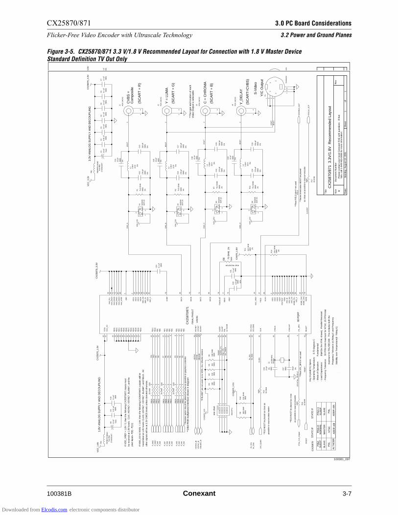
CX25870/871 3.0 PC Board Considerations
Flicker-Free Video Encoder with Ultrascale Technology 3.2 Power and Ground Planes
100381B Conexant 3-7
C10
0.1
uF08
05
C9
0.01
uF
0805
RN
1A33
OH
M16
321
8
L1 1.8u
H
1210 5%
J4 RC
A J
AC
K2
2
1
3
C23
1.0
uF08
05
10K
OH
M08
05
R9
L4 1.8u
H
1210 5%
C22
22 p
F
0805
5%
J1 RC
A J
AC
K2
2
1
3
C24
270
pF
0805
5%
R12
75.0
OH
M
0805
1%
C25
330
pF
0805
5%
C11
22 p
F
0805
5%
C12
270
pF
0805
5%
10K
0805
R3
10K
0805
R4
10K
0805
R5
J2 RC
A J
AC
K2
2
1
3
10K
OH
M08
05
R6
J3 RC
A J
AC
K2
2
1
3
Y1
13.5
00 M
Hz
HC
49U
D1
DA
204K
SO
T-2
3
2
3
1
C26
27 p
F
0805
C27
33 p
F
0805
R1
75.0
OH
M
0805
1%
10K
OH
M08
05
R11
R13
33 O
HM
0805
10K
OH
M08
05
R14
C13
330
pF
0805
5%
L2 1.8u
H
1210 5%
C15
22 p
F
0805
5%
L3 1.8u
H
1210 5%
R16
33 O
HM
0805
C16
270
pF
0805
5%
C18
22 p
F
0805
5%
C19
270
pF
0805
5%
C1
10 u
F
7343
+
R2
75.0
OH
M
0805
1%
C17
330
pF
0805
5%
R7
75.0
OH
M
0805
1%
FB
1
FE
RR
ITE
BE
AD
Fai
r-R
ite
C20
330
pF
0805
5%
C14
0.1
uF08
05
VA
A_D
AC
A69
FIE
LD37
VA
A_D
AC
C73
XT
ALI
N63
XT
ALO
UT
62
VS
S3
22V
SS
221
VD
D1
VA
A_D
AC
B71
VS
S5
41
VS
S1
4
RE
SE
T*
53
BLA
NK
*38
VS
YN
C*
36H
SY
NC
*35
PA
L50
SLA
VE
51S
LEE
P52
ALT
AD
DR
48
VS
S4
31
SIC
(S
CL)
45
SID
(S
DA
)44
CLK
I54
CLK
O56
VR
EF
76
VB
IAS
77
FS
AD
JUS
T78
DA
CC
72
DA
CB
70
DA
CA
68
CO
MP
75
VA
A_P
LL59
VA
A_D
AC
D67
DA
CD
66
XT
L_B
FO
3
VS
S_S
I42
P[1
5]24
P[1
4]23
P[1
3]18
P[1
2]17
P[1
1]16
P[1
0]15
P[9
]14
P[8
]13
P[7
]12
P[6
]11
P[5
]10
P[4
]9
P[3
]8
P[2
]7
P[1
]6
P[0
]5
P[1
6]25
P[1
7]26
P[1
8]27
P[1
9]28
P[2
0]29
P[2
1]32
P[2
2]33
P[2
3]34
VS
S_S
O43
VD
D_S
O46
VD
D_S
I47
VD
D_V
RE
F49
VS
S_C
O55
VD
D_C
O57
AG
ND
_PLL
58
VD
D5
60
VD
D_X
61
VS
S_X
64
AG
ND
_DA
C65
AG
ND
_DA
C74
AG
ND
79
VA
A_V
RE
F80
VD
DL
40
VD
D3
20V
DD
219
VD
D1
2
VD
D4
30
VS
S/T
ES
T39
CX
2587
0/87
1
FIN
AL
PIN
OU
T 1
/02/
01
80 P
QF
P
10K
OH
M08
05
R10
C3
0.1
uF08
05
C4
0.1
uF08
05
C5
0.1
uF08
05
C6
0.1
uF08
05
C7
1.0
uF08
05
RN
3A33
OH
M16
321
8
75 O
HM
, 1%
0805
R8
RN
3B2
7
RN
3C3
6
RN
3D4
5
C2
0.01
uF
0805
RN
2C3
6
P1
Con
nect
or
1 2 3 4
5
6
7
1
4
2
3
C21
0.1
uF08
05
RN
2B2
7
RN
2D4
5
D2
DA
204K
SO
T-2
3
2
3
1
D3
DA
204K
SO
T-2
3
2
3
1
RN
1C3
6
RN
1D4
5
D4
DA
204K
SO
T-2
3
2
3
1
RN
1B2
7
R17
33 O
HM
0805
SW
DIP
-4
1 2 3 4
8 7 6 5
C8
10 u
F
7343
+
FB
2
FE
RR
ITE
BE
AD
Fai
r-R
ite
RN
2A33
OH
M16
321
8
AO
UT
BO
UT
CO
UT
CO
UT
BO
UT
DO
UT
FIE
LD
P8
P10
SLE
EP
P11
CLK
OU
T
PA
L_C
TL
P3
CLK
IN
P4
P7
P9
CR
YS
TA
L_O
UT
PU
T
P5
RSET RESISTOR
3V_S
CL
P2
DA
C_D
HS
YN
C
RE
SE
T
P0
I2C
_AD
DR
VS
YN
C
DA
C_C
DA
C_B
3V_S
DASLA
VE
_CT
L
CB
LAN
K
P1
P6
DA
C_A
CX
2587
0_3.
3V
VA
A_3
.3V
VC
C_3
.3V
VC
C_1
.8V
VA
A_3
.3V
VA
A_3
.3V
VA
A_3
.3V
CX
2587
0_3.
3V
CX
2587
0_3.
3V
CX
870_
1.8V
CX
2587
0_1.
8V
CX
2587
0_3.
3V
HS
YN
C_B
I
VS
YN
C_B
I
CB
LAN
K_B
I
870_
CLK
IN
3V_S
DA
3V_S
CL RE
SE
T
870F
IELD
_OU
T
870C
LK_O
UT
P_I
N7
P_I
N3
P_I
N0
P_I
N2
P_I
N1
P_I
N4
P_I
N6
P_I
N5
P_I
N11
P_I
N8
P_I
N10
P_I
N9
XT
AL_
CLK
_Out
put
C =
CH
RO
MA
(SC
AR
T =
B)
CV
BS
=C
ompo
site
(SC
AR
T =
R)
Y =
LU
MA
(SC
AR
T =
G)
**24
bit R
GB
mul
tiple
xed
inte
rfac
e sh
own
in d
iagr
am
3.3V
AN
ALO
G S
UP
PLY
AN
D D
EC
OU
PLI
NG
2743
0214
47
S-V
ideo
Y/C
Out
put
If V
DD
_VR
EF
= 1
.8V
/ 2,
then
the
follo
win
g C
X25
870/
871
inpu
ts m
ust
be r
ecei
ved
at 1
.8V
leve
ls:
CLK
I, H
SY
NC
*, V
SY
NC
*, B
LAN
K*,
and
the
pixe
l inp
uts-
P[0
] - P
[11]
1.8V
AN
ALO
G S
UP
PLY
AN
D D
EC
OU
PLI
NG
2743
0214
47
Y_D
ELA
Y (S
CA
RT
=C
VB
S)
PA
L
MA
ST
ER
AD
DR
x88
SLE
EP
PA
L
NO
RM
AL
AD
DR
x8A
SLA
VE
ALT
AD
DR
ST
AT
E IF
PIN
#=0
SLE
EP
ST
AT
E IF
PIN
#=1
CX
2587
0
PIN
#:
SLA
VE
NT
SC
see
char
t
5% 5%
Key
Cry
stal
(Y1)
Spe
cs:
- O
pera
ting
Tem
pera
ture
: 0
-70
degr
ees
C -
Mod
e of
Ope
ratio
n:
F
unda
men
tal
- Lo
ad C
apac
itanc
e:
20pF
(for
the
XT
AL
show
n),
Par
alle
l Res
onan
t -
Fre
quen
cy T
oler
ance
:
50 P
PM
tota
l max
imum
for
NT
SC
; 25
PP
M to
tal
m
axim
um fo
r P
AL/
SE
CA
M.
Thi
s in
clud
es b
oth
the
F
requ
ency
Tol
eran
ce a
t 25d
eg.C
and
Fre
quen
cy
Sta
bilit
y ov
er T
empe
ratu
re(0
-70
deg.
C)
**F
loat
XT
L_B
FO
if n
ot u
sed
**T
he ty
pe a
nd lo
catio
n of
eac
hV
ideo
Out
put i
s se
lect
able
1%
1%
**R
esis
tor
pack
s sh
ould
be
plac
ed a
s cl
ose
as p
ossi
ble
to g
raph
ics
cont
rolle
r
10%
**S
erie
s te
rmin
atio
n M
US
T b
e pl
aced
as
clo
se a
s po
ssib
le to
sou
rce=
enco
der
If V
DD
_CO
& V
DD
L =
1.8
V, t
hen
the
follo
win
g C
X25
870/
871
outp
uts
will
be
tran
smitt
ed a
t 1.8
V le
vels
: CLK
O, H
SY
NC
*, V
SY
NC
*, B
LAN
K*,
and
FIE
LD.
All
othe
r si
gnal
s w
ill b
e at
3.3
V C
MO
S le
vels
unl
ess
deno
ted
othe
rwis
e.
**F
loat
FIE
LD p
in if
not
use
d
**R
13 M
US
T b
e pl
aced
as
clos
e as
poss
ible
to s
ourc
e=da
ta m
aste
r
**R
16 M
US
T b
e pl
aced
as
clos
e as
pos
sibl
e to
sou
rce=
enco
der
*If B
LAN
K*
pin
not u
sed,
tie
to V
DD
L th
ru 1
0koh
m r
esis
tor
100381_097
CX
2587
0/87
1 3
.3V
/1.8
V R
ecom
men
ded
Layo
ut
B
11
Mon
day,
Aug
ust 1
3, 2
001
Titl
e
Siz
eD
ocum
ent N
umbe
rR
ev
Dat
e:S
heet
of
Ple
ase
cont
act y
our
loca
l Con
exan
t FA
E w
ith q
uest
ions
. If
that
fails
, cal
l 1-9
49-4
83-6
996
for
mor
e in
form
atio
n.
Figure 3-5. CX25870/871 3.3 V/1.8 V Recommended Layout for Connection with 1.8 V Master Device Standard Definition TV Out Only
C10
0.1
uF08
05
C9
0.01
uF
0805
RN
1A33
OH
M16
321
8
L1 1.8u
H
1210 5%
J4 RC
A J
AC
K2
2
1
3
C23
1.0
uF08
05
10K
OH
M08
05
R9
L4 1.8u
H
1210 5%
C22
22 p
F
0805
5%
J1 RC
A J
AC
K2
2
1
3
C24
270
pF
0805
5%
R12
75.0
OH
M
0805
1%
C25
330
pF
0805
5%
C11
22 p
F
0805
5%
C12
270
pF
0805
5%
10K
0805
R3
10K
0805
R4
10K
0805
R5
J2 RC
A J
AC
K2
2
1
3
10K
OH
M08
05
R6
J3 RC
A J
AC
K2
2
1
3
Y1
13.5
00 M
Hz
HC
49U
D1
DA
204K
SO
T-2
3
2
3
1
C26
27 p
F
0805
C27
33 p
F
0805
R1
75.0
OH
M
0805
1%
10K
OH
M08
05
R11
R13
33 O
HM
0805
10K
OH
M08
05
R14
C13
330
pF
0805
5%
L2 1.8u
H
1210 5%
C15
22 p
F
0805
5%
L3 1.8u
H
1210 5%
R16
33 O
HM
0805
C16
270
pF
0805
5%
C18
22 p
F
0805
5%
C19
270
pF
0805
5%
C1
10 u
F
7343
+
R2
75.0
OH
M
0805
1%
C17
330
pF
0805
5%
R7
75.0
OH
M
0805
1%
FB
1
FE
RR
ITE
BE
AD
Fai
r-R
ite
C20
330
pF
0805
5%
C14
0.1
uF08
05
VA
A_D
AC
A69
FIE
LD37
VA
A_D
AC
C73
XT
ALI
N63
XT
ALO
UT
62
VS
S3
22V
SS
221
VD
D1
VA
A_D
AC
B71
VS
S5
41
VS
S1
4
RE
SE
T*
53
BLA
NK
*38
VS
YN
C*
36H
SY
NC
*35
PA
L50
SLA
VE
51S
LEE
P52
ALT
AD
DR
48
VS
S4
31
SIC
(S
CL)
45
SID
(S
DA
)44
CLK
I54
CLK
O56
VR
EF
76
VB
IAS
77
FS
AD
JUS
T78
DA
CC
72
DA
CB
70
DA
CA
68
CO
MP
75
VA
A_P
LL59
VA
A_D
AC
D67
DA
CD
66
XT
L_B
FO
3
VS
S_S
I42
P[1
5]24
P[1
4]23
P[1
3]18
P[1
2]17
P[1
1]16
P[1
0]15
P[9
]14
P[8
]13
P[7
]12
P[6
]11
P[5
]10
P[4
]9
P[3
]8
P[2
]7
P[1
]6
P[0
]5
P[1
6]25
P[1
7]26
P[1
8]27
P[1
9]28
P[2
0]29
P[2
1]32
P[2
2]33
P[2
3]34
VS
S_S
O43
VD
D_S
O46
VD
D_S
I47
VD
D_V
RE
F49
VS
S_C
O55
VD
D_C
O57
AG
ND
_PLL
58
VD
D5
60
VD
D_X
61
VS
S_X
64
AG
ND
_DA
C65
AG
ND
_DA
C74
AG
ND
79
VA
A_V
RE
F80
VD
DL
40
VD
D3
20V
DD
219
VD
D1
2
VD
D4
30
VS
S/T
ES
T39
CX
2587
0/87
1
FIN
AL
PIN
OU
T 1
/02/
01
80 P
QF
P
10K
OH
M08
05
R10
C3
0.1
uF08
05
C4
0.1
uF08
05
C5
0.1
uF08
05
C6
0.1
uF08
05
C7
1.0
uF08
05
RN
3A33
OH
M16
321
8
75 O
HM
, 1%
0805
R8
RN
3B2
7
RN
3C3
6
RN
3D4
5
C2
0.01
uF
0805
RN
2C3
6
P1
Con
nect
or
1 2 3 4
5
6
7
1
4
2
3
C21
0.1
uF08
05
RN
2B2
7
RN
2D4
5
D2
DA
204K
SO
T-2
3
2
3
1
D3
DA
204K
SO
T-2
3
2
3
1
RN
1C3
6
RN
1D4
5
D4
DA
204K
SO
T-2
3
2
3
1
RN
1B2
7
R17
33 O
HM
0805
SW
DIP
-4
1 2 3 4
8 7 6 5
C8
10 u
F
7343
+
FB
2
FE
RR
ITE
BE
AD
Fai
r-R
ite
RN
2A33
OH
M16
321
8
AO
UT
BO
UT
CO
UT
CO
UT
BO
UT
DO
UT
FIE
LD
P8
P10
SLE
EP
P11
CLK
OU
T
PA
L_C
TL
P3
CLK
IN
P4
P7
P9
CR
YS
TA
L_O
UT
PU
T
P5
RSET RESISTOR3V
_SC
L
P2
DA
C_D
HS
YN
C
RE
SE
T
P0
I2C
_AD
DR
VS
YN
C
DA
C_C
DA
C_B
3V_S
DASLA
VE
_CT
L
CB
LAN
K
P1
P6
DA
C_A
CX
2587
0_3.
3V
VA
A_3
.3V
VC
C_3
.3V
VC
C_1
.8V
VA
A_3
.3V
VA
A_3
.3V
VA
A_3
.3V
CX
2587
0_3.
3V
CX
2587
0_3.
3V
CX
870_
1.8V
CX
2587
0_1.
8V
CX
2587
0_3.
3V
HS
YN
C_B
I
VS
YN
C_B
I
CB
LAN
K_B
I
870_
CLK
IN
3V_S
DA
3V_S
CL RE
SE
T
870F
IELD
_OU
T
870C
LK_O
UT
P_I
N7
P_I
N3
P_I
N0
P_I
N2
P_I
N1
P_I
N4
P_I
N6
P_I
N5
P_I
N11
P_I
N8
P_I
N10
P_I
N9
XT
AL_
CLK
_Out
put
C =
CH
RO
MA
(SC
AR
T =
B)
CV
BS
=C
ompo
site
(SC
AR
T =
R)
Y =
LU
MA
(SC
AR
T =
G)
**24
bit R
GB
mul
tiple
xed
inte
rfac
e sh
own
in d
iagr
am
3.3V
AN
ALO
G S
UP
PLY
AN
D D
EC
OU
PLI
NG
2743
0214
47
S-V
ideo
Y/C
Out
put
If V
DD
_VR
EF
= 1
.8V
/ 2,
then
the
follo
win
g C
X25
870/
871
inpu
ts m
ust
be r
ecei
ved
at 1
.8V
leve
ls:
CLK
I, H
SY
NC
*, V
SY
NC
*, B
LAN
K*,
and
the
pixe
l inp
uts-
P[0
] - P
[11]
1.8V
AN
ALO
G S
UP
PLY
AN
D D
EC
OU
PLI
NG
2743
0214
47
Y_D
ELA
Y (S
CA
RT
=C
VB
S)
PA
L
MA
ST
ER
AD
DR
x88
SLE
EP
PA
L
NO
RM
AL
AD
DR
x8A
SLA
VE
ALT
AD
DR
ST
AT
E IF
PIN
#=0
SLE
EP
ST
AT
E IF
PIN
#=1
CX
2587
0
PIN
#:
SLA
VE
NT
SC
see
char
t
5% 5%
Key
Cry
stal
(Y1)
Spe
cs:
- O
pera
ting
Tem
pera
ture
: 0
-70
degr
ees
C -
Mod
e of
Ope
ratio
n:
F
unda
men
tal
- Lo
ad C
apac
itanc
e:
20pF
(for
the
XT
AL
show
n),
Par
alle
l Res
onan
t -
Fre
quen
cy T
oler
ance
:
50 P
PM
tota
l max
imum
for
NT
SC
; 25
PP
M to
tal
m
axim
um fo
r P
AL/
SE
CA
M.
Thi
s in
clud
es b
oth
the
F
requ
ency
Tol
eran
ce a
t 25d
eg.C
and
Fre
quen
cy
Sta
bilit
y ov
er T
empe
ratu
re(0
-70
deg.
C)
**F
loat
XT
L_B
FO
if n
ot u
sed
**T
he ty
pe a
nd lo
catio
n of
eac
hV
ideo
Out
put i
s se
lect
able
1%
1%
**R
esis
tor
pack
s sh
ould
be
plac
ed a
s cl
ose
as p
ossi
ble
to g
raph
ics
cont
rolle
r
10%
**S
erie
s te
rmin
atio
n M
US
T b
e pl
aced
as
clo
se a
s po
ssib
le to
sou
rce=
enco
der
If V
DD
_CO
& V
DD
L =
1.8
V, t
hen
the
follo
win
g C
X25
870/
871
outp
uts
will
be
tran
smitt
ed a
t 1.8
V le
vels
: CLK
O, H
SY
NC
*, V
SY
NC
*, B
LAN
K*,
and
FIE
LD.
All
othe
r si
gnal
s w
ill b
e at
3.3
V C
MO
S le
vels
unl
ess
deno
ted
othe
rwis
e.
**F
loat
FIE
LD p
in if
not
use
d
**R
13 M
US
T b
e pl
aced
as
clos
e as
poss
ible
to s
ourc
e=da
ta m
aste
r
**R
16 M
US
T b
e pl
aced
as
clos
e as
pos
sibl
e to
sou
rce=
enco
der
*If B
LAN
K*
pin
not u
sed,
tie
to V
DD
L th
ru 1
0koh
m r
esis
tor
100381_097
CX
2587
0/87
1 3
.3V
/1.8
V R
ecom
men
ded
Layo
ut
B
11
Mon
day,
Aug
ust 1
3, 2
001
Titl
e
Siz
eD
ocum
ent N
umbe
rR
ev
Dat
e:S
heet
of
Ple
ase
cont
act y
our
loca
l Con
exan
t FA
E w
ith q
uest
ions
. If
that
fails
, cal
l 1-9
49-4
83-6
996
for
mor
e in
form
atio
n.
Downloaded from Elcodis.com electronic components distributor
3.0 PC Board Considerations CX25870/871
3.3 Recommended Schematics and Layout for CX25870/871 Flicker-Free Video Encoder with Ultrascale Technology
3-8 Conexant 100381B
3.3 Recommended Schematics and Layout for CX25870/871
For the CX25870/871 to operate at an optimal technical level, it is imperative to
adopt the passive components, values, tolerances, and guidelines contained in the
following figures.
Conexant has done extensive lab testing with these components, and found
that they yield the best combination of performance and price.
The complete schematic diagram for a 3.3 V only design is illustrated in
Figure 3-4.
The complete schematic diagram for a mixed 3.3 V and 1.8 V design
environment is illustrated in Figure 3-5.
For a complete schematic diagram for a mixed 3.3V and lower voltage (1.5 V
or 1.1 V) design environment, request assistance from your local FAE. The
finished schematic for the 3.3 V/1.5 V or 3.3 V/1.1 V case will look similar to
Figure 3-5.
Substitution of resistors, capacitors, inductors, and crystals with
nonrecommended values or greater than recommended tolerances may degrade
the video output quality of the CX25870/871 encoder.
Downloaded from Elcodis.com electronic components distributor
CX25870/871 3.0 PC Board Considerations
Flicker-Free Video Encoder with Ultrascale Technology 3.4 Decoupling
100381B Conexant 3-9
3.4 Decoupling
3.4.1 Device Decoupling
For optimum performance, all capacitors should be located as close as possible to
the device, and the shortest possible leads (consistent with reliable operation)
should be used to reduce the lead inductance. Chip capacitors are recommended
for minimum lead inductance. Radial lead ceramic capacitors can be substituted
for chip capacitors and are better than axial lead capacitors for self-resonance.
Values are chosen to have self-resonance above the pixel clock.
3.4.2 Power Supply Decoupling
The best power supply performance is obtained with a 0.1 !F ceramic capacitor
decoupling each group of VAA pins and each group of VDD pins to GND. The
capacitors should be placed as close as possible to the device VAA/VDD pins and
GND pins and connected with short, wide traces.
The 47 !F capacitor shown in Figure 3-2 is for low-frequency power supply
ripple; the 0.1 !F capacitors are for high-frequency power supply noise rejection.
Inclusion of a 0.01 !F and a 1.0 !F capacitor between the group of VAA/VDD
pins and GND/VSS pins will improve power supply decoupling at intermediate
frequencies as well.
When a linear regulator is used, the proper power-up sequence must be
verified to prevent latchup. A linear regulator is recommended to filter the analog
power supply if the power supply noise is greater than or equal to 200 mV. This is
especially important when a switching power supply is used, or low voltage
interface is implemented, and the switching frequency is close to the raster scan
frequency. About 5 percent of the power supply hum and ripple noise less than
1 MHz will couple onto the analog outputs.
3.4.3 COMP Decoupling
The COMP pin must be decoupled to the closest VAA pin, typically with a 0.1 !F
ceramic capacitor. Low-frequency supply noise will require a larger value. The
COMP capacitor must be as close as possible to the COMP and VAA pins. A
surface-mount ceramic chip capacitor is preferred for minimal lead inductance.
Lead inductance degrades the noise rejection of the circuit. Short, wide traces will
also reduce lead inductance.
3.4.4 VREF Decoupling
A 1.0 !F ceramic capacitor should be used to decouple this input to GND.
3.4.5 VBIAS Decoupling
A 0.1 !F ceramic capacitor should be used to decouple this output to GND.
Downloaded from Elcodis.com electronic components distributor
3.0 PC Board Considerations CX25870/871
3.5 Signal Interconnect Flicker-Free Video Encoder with Ultrascale Technology
3-10 Conexant 100381B
3.5 Signal Interconnect
3.5.1 Digital Signal Interconnect
The digital inputs to the CX25870/871 should be isolated as much as possible
from the analog outputs and other analog circuitry. Also, these input signals
should not overlay the analog power plane or analog output signals.
Most of the noise on the analog outputs will be caused by fast transitioning
clock edges, data edges (less than 3 ns), and overshoot, undershoot, and ringing
on the digital inputs.
The digital edge rates should not be faster than necessary because feedthrough
noise is proportional to the digital edge rates. Lower-speed applications will
benefit from using lower-speed logic (3–5 ns edge rates) to reduce data-related
noise on the analog outputs.
Transmission lines will mismatch if the lines do not match the source and
destination impedance. This will degrade signal fidelity if the line length
reflection time is greater than one-fourth the signal edge time. Line termination or
line-length reduction is the solution. For example, logic edge rates of 2 ns require
line lengths of less than 4 inches without use of termination. Ringing can be
reduced by damping the line with a series resistor (30–50 ").
Radiation of digital signals can also be picked up by the analog circuitry. This
is prevented by reducing the digital edge rates (rise/fall time), minimizing ringing
with damping resistors, and minimizing coupling through PC board capacitance
by routing the digital signals at a 90-degree angle to any analog signals.
The clock driver and all other digital devices must be adequately decoupled to
prevent noise generated by the digital devices from coupling into the analog
circuitry.
3.5.2 Analog Signal Interconnect
The CX25870/871 analog output traces should be located as close as possible to
the output connectors and be of equal length to minimize noise pickup and
reflections caused by impedance mismatch.
The analog outputs are susceptible to crosstalk from digital lines; therefore
digital traces must not be routed under or adjacent to the analog output traces.
To maximize the high-frequency power supply rejection, the video output
signals should overlay the ground plane.
For maximum performance, the analog video output impedance, cable
impedance, and load impedance should be the same. The load resistor connection
between the video outputs and GND should be as close as possible to the
CX25870/871 to minimize reflections. Unused DAC analog outputs should be left
floating.
Downloaded from Elcodis.com electronic components distributor
CX25870/871 3.0 PC Board Considerations
Flicker-Free Video Encoder with Ultrascale Technology 3.6 Applications Information
100381B Conexant 3-11
3.6 Applications Information
3.6.1 Changes Required to Accommodate CX25870/871 in Bt868/869-Designs
3.6.1.1 Software The CX25870/871 is software backward compatible with Conexant’s first
generation VGA Encoder, the Bt868/869. This means that all register indices for
the Bt868/869 were carried forward to the exact same indices for the
CX25870/871. For Conexant’s second generation encoder, new registers were
added, but the actual addresses used were outside of the 0x6C to 0xD6 range
reserved for the Bt868/869 legacy functionality. Some reserved bits within the
Bt868/869 did take on significance with the CX25870/871 where necessary.
The most significant difference in software between the two encoders is the
fact that the CX25870/871 can be read from using the Standard serial method as
well as the Legacy serial method. To use the Standard procedure, the master
issues CX25870’s device ID and subaddress in consecutive bytes, and the slave
acknowledges with a pulse after each transaction. Upon completion of these 2
steps, the slave transmits the final byte which contains the 8 bits of data. The
Bt868/869 cannot be read from in this manner and instead relies solely on the
Legacy method. This process is explained step-by-step in the ‘TV Auto-Detection
Procedures’ section of this specification.
Another difference in terms of software between the two encoders is the
power-up video output routing. The CX25870 after power-up or a signal-driven
reset transmits Video0 = composite on DAC_A, Video1 = Luma (Y) on DAC_B,
Video2 = Chroma (C) on DAC_C, and Video3 = Luma Delay on DAC_D.
The Bt868 was different in this respect. On power-up, it sent out
Video0 = composite from DAC_A, DAC_B, and DAC_C. Reprogramming
register 0xCE correctly ensures proper video output routing.
Table 3-2. Relative Register Map for CX25870/871
Shared CX25870/871 & Bt868/869 registers
Register Addresses 0x00 to 0x04 (Read Only)
(Must be accessed through ‘Legacy’ read procedure with ESTATUS[1:0] bits in Bt868/869)
(‘Standard’ or ‘Legacy’ read-back procedure ok for CX25870/871)
CX25870/871 specific registers
Register Address 0x06(Read Only)
and
Register Addresses 0x28E to 0x6A (Read/Write)
Shared CX25870/871 & Bt868/869 registers
Register Address 0x6C(Read/Write)
to
Register Address 0xD6(Read/Write)
CX25870/871 specific register
Register Address 0xD8(Read/Write)
Downloaded from Elcodis.com electronic components distributor
3.0 PC Board Considerations CX25870/871
3.6 Applications Information Flicker-Free Video Encoder with Ultrascale Technology
3-12 Conexant 100381B
Another difference between the two encoders is the default video output
routing through the on-chip DACs. On power-up, the Bt868 transmitted Video[0]
= Composite from all three of its DACs. Due to the popularity of S-Video out, the
CX25871, on power-up, broadcasts Video[0] = Composite from DAC_A,
Video[1] = Luminance from DAC_B, Video[2] = Chrominance from DAC_C,
and Video[3] = Delayed Luminance from DAC_D. For Bt868 drivers that did not
program register 0xCE, this step may be necessary to re-route the Video outputs
with the CX25870.
As a result of software register compatibility, no modifications to a customer’s
source code are required to enable the same features that exist within both
Conexant VGA encoders. Of course, to exploit the new features within the
CX25870/871, such as display of 1024x768 resolution on a TV, HDTV output,
SECAM output, and others, some software changes and new register sets will be
necessary. This usually equates to the release of a new driver and/or graphics
BIOS for support of the CX25870.
3.6.1.2 Hardware Similarly, the Bt868/869 is pin-for-pin backward compatible with the newest
Conexant encoder. Both devices are housed in exactly the same compact 80-pin,
[14 mm x 14 mm x 2.4 mm] plastic PQFP package. Furthermore, aside from pins
2, 3, 65, 66, and 67, which were no connects within the Bt868/869, the
CX25870/871 is identical in its pinout to the previous generation.
Consequently, if the customer’s Bt868-designed PCB actually has no connects
for the pins listed as N/C on the Bt868/869, then no PC board changes are needed
except for some passive component stuffing changes when upgrading to the
CX25870/871. However, if the Bt868/869 N/C pins were actually grounded or
utilization of the new external features within the CX25870/871 is desired, then a
few changes to a customer’s Bt868/869-based PC Board are definitely required to
accommodate the new CX25870/871. Table 3-3 summarizes all the likely
alterations that need to be performed to existing designs.
Table 3-3. Hardware Modifications to Bt868/869-based PCB Required to Accommodate the CX25870/871 (1 of 3)
Pin #
Bt868/9 Pin Name
CX25870/1Pin Name
Comment
1 AGND VDD This pin should be tied to VDD (3.3V) for both the CX25870/1 and Bt868/9, so the encoder’s output video levels match the IRE levels that it was designed to transmit.
Conexant has seen 2-3 IRE excursions away from the correct color bar and other test pattern IRE levels and have verified that either encoder's pin #1 being tied to GND to be
the root cause.An output video difference of 2-3 IRE is a very small amplitude AND would only be noticeable if you used a VM700T from Tektronix or some other advanced piece of video
measuring equipment. Visually, it is quite difficult to even detect a 2-3 IRE excursion.In conclusion, tie Pin #1 which was the Bt868/9’s ‘AGND’ to VDD/VAA = 3.3V for both the CX25870/1 and Bt868/9 for best operation. Rename this pin (#1) on any
schematics so it says 'VDD.’
2 N/C VDD The digital power pin needs to be tied to 3.3V. This was a no connect for the Bt868/9.
3 N/C XTL_BFO The buffered crystal clock output pin should be floated if not used. This was a no connect for the Bt868/9.
For CX25870/1-designs, a small (e.g. 33 ohm) series resistor should be added in series to XTL_BFO as close as possible to the signal source device. This reduces overshoot and undershoot on this signal as it changes states.
Downloaded from Elcodis.com electronic components distributor
CX25870/871 3.0 PC Board Considerations
Flicker-Free Video Encoder with Ultrascale Technology 3.6 Applications Information
100381B Conexant 3-13
49 VDDMAX VDD_VREF Pin 49 has been renamed for the CX25870/1. For 3.3V swings on the interface signals for CX25870/1-designs, this pin should be tied directly to 3.3V as was the case with Bt868/9-designs.
For lower voltage swings for the digital interface signals, using a voltage divider circuit or some other method, tie the CX25870/871’s VDD_VREF input (pin 49) to (VDDL / 2). See Figure 3-5 for an illustration of this concept.
50 PAL PAL If the desired video output at power-up is PAL, then a 10 k" pull-up resistor is recommended for this pin for CX25870/1-designs. No pull-up resistor was advocated
for Bt868/9-designs. If the desired video output at power-up is NTSC, then this pin should be tied directly to GND.
51 SLAVE SLAVE If desired interface at power-up is slave or pseudo-master (i.e. slave video timing), then a 10 k" pull-up resistor is recommended for this pin for CX25870/1-designs. No pull-up resistor was advocated for Bt868/9-designs. If desired interface at power-up is
master (i.e. master video timing), then this pin should be tied directly to GND.
52 SLEEP SLEEP If desired power management state at power-up is Normal Operation, then this pin
should be tied directly to GND. If desired power management state at power-up is Sleep, then a 10 k" pull-up resistor is recommended for this pin for CX25870/1-designs. No pull-up resistor was advocated for Bt868/9-designs.
6263
XTALOUTXTALIN
XTALOUTXTALIN
The recommended capacitor value from XTALIN to GND has been altered from 33 pF to 27 pF for a 20 pF load crystal. This ensures an output-to-input voltage gain sufficient to
make up signal losses through the crystal since the ratio ofCXTALOUT / CXTALIN = 1.1 to 1.5.
The buffered clock crystal output frequency, which can be measured from the CX25870/1's XTL_BFO output port, should be within 25 ppM = +/- 337 Hz. of 13.5000
MHz. at all times. The high amount of tolerance is necessary so the encoder can generate sufficient accuracy for the subcarrier frequencies for SECAM, PAL, and NTSC. If this type of accuracy does not exist when using CXTALIN = 27 pF then CXTALIN should
be increased to 30 pF or 33 pF and the frequency re-measured. Different PCBs exhibit different amounts of parasitic capacitance so one value for CXTALIN does not
necessarily fit for all designs.
For Bt868/9-designs, CXTALIN and CXTALOUT were recommended to be equal (33 pF).
The 1 M" resistor, a requirement of Bt868/9-designs as an external passive between
these 2 pins, is no longer necessary with CX25870/1-designs. If it is present, then this has no adverse effects on the CX25870/1’s overall video performance.
65 N/C AGND_DAC Whether or not DACD is actually used as a video output within the CX25870/1 design, this pin must be tied to GND.For Bt868/9-based designs, this pin was a No Connect and for best performance
should be tied to GND or left open.
66 N/C DACD Pin 66 for the CX25870/1 is the fourth DAC = DACD.If DACD is used, connect this output to a video connector. If DACD is not used, leave this pin no connected for CX25870/1-designs. The circuitry for the low pass filter for
DACD will also need to be added for CX25870/1 designs.For Bt868/9-based designs, this pin was a No Connect and for best performance should be tied to GND or left open.
67 N/C VAA_DACD This is the power pin for DACD. Whether or not DACD is actually used within the design, this pin must be tied to VDD=VAA=3.3V for all CX25870/1-designs.
For Bt868/9-based designs, this pin was a No Connect and for best performance should be tied to GND or left open.
Table 3-3. Hardware Modifications to Bt868/869-based PCB Required to Accommodate the CX25870/871 (2 of 3)
Downloaded from Elcodis.com electronic components distributor

3.0 PC Board Considerations CX25870/871
3.6 Applications Information Flicker-Free Video Encoder with Ultrascale Technology
3-14 Conexant 100381B
To ensure proper operation of the CX25870/871, the designer must adhere to
each recommendation contained in Table 3-3.
75 COMP COMP A 0-10 ohm resistor between COMP and 0.1 !F capacitor (which is connected to VAA) was originally recommended for Bt868/9-designs.The 0-10 ohm resistor placed between the 0.1 !F cap and the COMP pin was
recommended to better tune the COMP circuit to prevent an internal op-amp from oscillating. Based on the Bt868/9's DAC performance over time and the CX25870/1's continued usage of these same DACs, this resistor was deemed to not be necessary
and should be removed for all CX25870/1 designs.
76 VREF VREF Capacitor from VREF to GND must be 1.0 !F for the CX25870/1. Capacitor from VREF
to GND must be 0.1 !F for the Bt868/9.
78 FSADJUST FSADJUST RSET, the resistor from FSADJUST pin to GND, must be 75 ", +/- 1% for all
CX25870/1-based designs.RSET must be 100 ohm, +/- 1% for all Bt868/9-based designs.
NOTE(S):
N/C = No connect
Table 3-3. Hardware Modifications to Bt868/869-based PCB Required to Accommodate the CX25870/871 (3 of 3)
Downloaded from Elcodis.com electronic components distributor
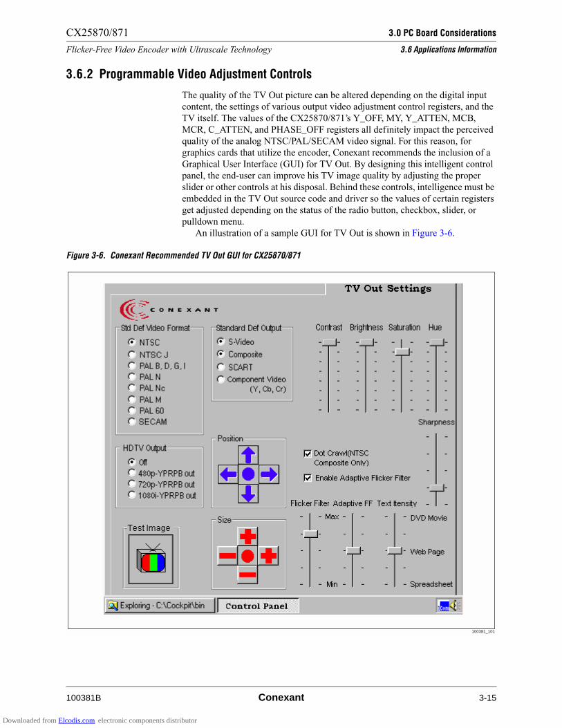
CX25870/871 3.0 PC Board Considerations
Flicker-Free Video Encoder with Ultrascale Technology 3.6 Applications Information
100381B Conexant 3-15
3.6.2 Programmable Video Adjustment Controls
The quality of the TV Out picture can be altered depending on the digital input
content, the settings of various output video adjustment control registers, and the
TV itself. The values of the CX25870/871’s Y_OFF, MY, Y_ATTEN, MCB,
MCR, C_ATTEN, and PHASE_OFF registers all definitely impact the perceived
quality of the analog NTSC/PAL/SECAM video signal. For this reason, for
graphics cards that utilize the encoder, Conexant recommends the inclusion of a
Graphical User Interface (GUI) for TV Out. By designing this intelligent control
panel, the end-user can improve his TV image quality by adjusting the proper
slider or other controls at his disposal. Behind these controls, intelligence must be
embedded in the TV Out source code and driver so the values of certain registers
get adjusted depending on the status of the radio button, checkbox, slider, or
pulldown menu.
An illustration of a sample GUI for TV Out is shown in Figure 3-6.
Figure 3-6. Conexant Recommended TV Out GUI for CX25870/871
100381_101
Downloaded from Elcodis.com electronic components distributor
3.0 PC Board Considerations CX25870/871
3.6 Applications Information Flicker-Free Video Encoder with Ultrascale Technology
3-16 Conexant 100381B
3.6.2.1 Contrast Contrast is a video quality that refers to how far the whitest whites are from the
blackest blacks in an analog video waveform. If the peak white is far away from
the peak black, the image is said to have high contrast. With high contrast, the
image is very pure like a black and white tile floor. If the two parameters are very
close together, the image is said to have poor, or low, contrast. With low amounts
of contrast, an image may be referred to as being washed-out. Instead of easily
recognized black portions of the image versus white parts, the image with low
contrast looks gray.
Register MY[7:0] in conjunction with register Y_ATTENUATE[2:0] controls
adjustment of contrast. Y_ATTENUATE has 8 possible values ranging from 1.0
gain (No attenuation) to 0 gain (Force Luminance to 0). Conexant recommends
inclusion of an 8-level slider to control the Contrast level. Each single movement
of the slider should reprogram this bit field to a different fractional value. Lab
testing has shown that values from ¾ gain (Y_ATTENUATE=011) to 15/16 gain
(i.e., 001) yield the crispest TV picture.
Register MY modifies the luminance multiplier allowing for a larger or
smaller luminance range. For more drastic changes in the Contrast, change MY.
For more subtle changes, shifting the Y_OFF register as the end-user moves the
slider should be sufficient.
Since the difference between contrast and brightness is usually understood by
video professionals only, Conexant recommends the designer increment or
decrement the YATTENUATE[2:0] field for either brightness or contrast
adjustments.
3.6.2.2 Saturation Saturation is the amount of color present. For example, a lightly saturated green
looks olive-green to gray while a fully saturated green looks like the color of a
pine tree. Saturation does not mean the brightness of a color, just how much
pigment is used to make the color itself. The less pigment, the less saturated the
color is, effectively adding white to the pure color.
The amount of Saturation is controlled by the bit field named
CATTENUATE[2:0]. CATTENUATE has eight possible values ranging from 1.0
gain (No attenuation) to 0 gain (Force Chrominance to 0). Conexant recommends
inclusion of an 8-level slider to control Saturation level. Each single movement of
the slider should reprogram this bit field to a different fractional value. Lab
testing has shown that values from ¾ gain (CATTENUATE=011) to 1.0 gain (i.e.,
000) yield the crispest TV picture.
3.6.2.3 Brightness Brightness is defined to be the intensity of the video level and refers to how much
light is emitted from the display. The amount of Brightness is controlled by the
register named Y_OFF[7:0].
Y_OFF[7:0] is a 2s complement number, such that a value of 0x00 is 0 IRE
offset, a value of 0x7F is an increase of 22.14 IRE above black level. Active video
will then be added to the offset level set by the Y_OFF value.
Since the difference between contrast and brightness is usually understood by
video professionals only, Conexant recommends the designer increment or
decrement the YATTENUATE[2:0] field for either brightness or contrast
adjustments.
Downloaded from Elcodis.com electronic components distributor
CX25870/871 3.0 PC Board Considerations
Flicker-Free Video Encoder with Ultrascale Technology 3.6 Applications Information
100381B Conexant 3-17
3.6.2.4 Hue Hue refers to the wavelength of the color. That means that hue is the term used to
represent the base color–red, green, magenta, yellow, and so forth. Hue is
completely separate from the intensity or the saturation of the color. For example,
a red hue could look brown at low saturation, fire-engine red at a higher level of
saturation, or pink at a high brightness level. All three colors have the same hue
however.
Occasionally, the end user may need to alter the hue. The method for adjusting
this parameter with the CX25870/871 is to program a different value to the
HUE_ADJ register. This method changes the hue in the composite and S-Video
signals for NTSC, PAL, and SECAM waveforms according to the following
equation:
Desired Phase Offset (in degrees) = [360' / 256] * (HUE_ADJ)
A slider labeled ‘HUE’ should be included in the GUI so minor alterations
(±20') in this parameter are possible. Major alterations(>20') in the phase offset
are not recommended since dramatic hue shifts will result in different colors than
the original.
3.6.2.5 Sharpness Occasionally, drastic phase shifts occur at the borders of dialog boxes within
applications programs and with certain combinations of text and background
colors. This is due to the primary and secondary colors being at opposite ends of
the UV hue spectrum. The result of these phase differences is that the edges or
text look blurry to the observer.
The CX25870/871 has a bit field available named PKFIL_SEL[1:0] to
sharpen these edges so they look crisper on the television. Four choices are
available, each of which enables a different type of peaking filter. The 0 dB
(Bypass) filter is the defaulted level while gains of 1 dB, 2 dB, and 3.5 dB are also
possible.
3.6.2.6 Dot Crawl Dot crawl refers to a specific image artifact that is the result of the NTSC
standard. When some computer generated text shows up on top of a video clip
being shown, close viewing of the TV will show some pixels or jaggies rolling up
or down the picture in the area of a dialog box’s edges. Another term for this
phenomenon is creepy-crawlies or the zipper effect.
Conexant has derived software code to minimize the dot crawl. This is not a
register or bit within the CX25870/871 but rather a complicated software
algorithm that modifies the 90-degree color subcarrier shift exhibited in four
consecutive NTSC fields. To obtain this code, file a request with your local
Conexant sales office. The algorithm/function for dot crawl should be enabled
with the NTSC Composite output only. It will have no effect for PAL or SECAM
outputs.
Downloaded from Elcodis.com electronic components distributor
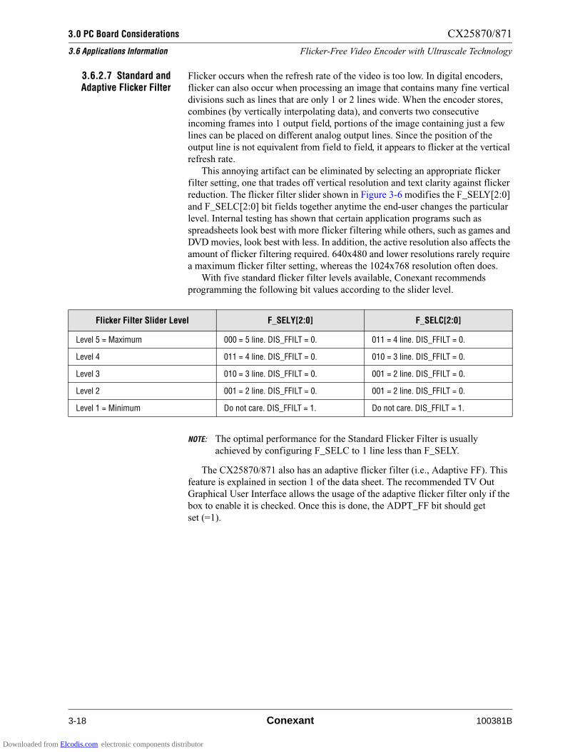
3.0 PC Board Considerations CX25870/871
3.6 Applications Information Flicker-Free Video Encoder with Ultrascale Technology
3-18 Conexant 100381B
3.6.2.7 Standard andAdaptive Flicker Filter
Flicker occurs when the refresh rate of the video is too low. In digital encoders,
flicker can also occur when processing an image that contains many fine vertical
divisions such as lines that are only 1 or 2 lines wide. When the encoder stores,
combines (by vertically interpolating data), and converts two consecutive
incoming frames into 1 output field, portions of the image containing just a few
lines can be placed on different analog output lines. Since the position of the
output line is not equivalent from field to field, it appears to flicker at the vertical
refresh rate.
This annoying artifact can be eliminated by selecting an appropriate flicker
filter setting, one that trades off vertical resolution and text clarity against flicker
reduction. The flicker filter slider shown in Figure 3-6 modifies the F_SELY[2:0]
and F_SELC[2:0] bit fields together anytime the end-user changes the particular
level. Internal testing has shown that certain application programs such as
spreadsheets look best with more flicker filtering while others, such as games and
DVD movies, look best with less. In addition, the active resolution also affects the
amount of flicker filtering required. 640x480 and lower resolutions rarely require
a maximum flicker filter setting, whereas the 1024x768 resolution often does.
With five standard flicker filter levels available, Conexant recommends
programming the following bit values according to the slider level.
NOTE: The optimal performance for the Standard Flicker Filter is usually
achieved by configuring F_SELC to 1 line less than F_SELY.
The CX25870/871 also has an adaptive flicker filter (i.e., Adaptive FF). This
feature is explained in section 1 of the data sheet. The recommended TV Out
Graphical User Interface allows the usage of the adaptive flicker filter only if the
box to enable it is checked. Once this is done, the ADPT_FF bit should get
set (=1).
Flicker Filter Slider Level F_SELY[2:0] F_SELC[2:0]
Level 5 = Maximum 000 = 5 line. DIS_FFILT = 0. 011 = 4 line. DIS_FFILT = 0.
Level 4 011 = 4 line. DIS_FFILT = 0. 010 = 3 line. DIS_FFILT = 0.
Level 3 010 = 3 line. DIS_FFILT = 0. 001 = 2 line. DIS_FFILT = 0.
Level 2 001 = 2 line. DIS_FFILT = 0. 001 = 2 line. DIS_FFILT = 0.
Level 1 = Minimum Do not care. DIS_FFILT = 1. Do not care. DIS_FFILT = 1.
Downloaded from Elcodis.com electronic components distributor
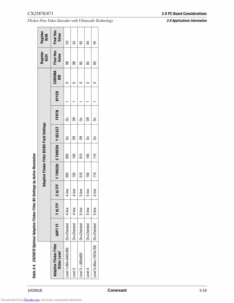
CX25870/871 3.0 PC Board Considerations
Flicker-Free Video Encoder with Ultrascale Technology 3.6 Applications Information
100381B Conexant 3-19
Tab
le 3
-4.
CX
25
87
0 O
pti
ma
l A
da
pti
ve F
lick
er
Fil
ter
Bit
Se
ttin
gs
by
Act
ive
Re
solu
tio
n
Ad
ap
tive
Fli
cke
r F
ilte
r B
it/B
it F
ield
Se
ttin
gs
Re
gis
ter
0x3
4R
eg
iste
r 0x3
6
Adapti
ve F
lick
er
Fil
ter
Sli
de
r L
eve
lA
DP
T F
FY
AL
TF
FC
AL
TF
FY
TH
RE
SH
C T
HR
ES
HY
SE
LE
CT
FF
RT
NB
YY
CR
CH
RO
MA
B
WF
inal
Hex
Va
lue
Fin
al
He
x V
alu
e
Lev
el 1
=M
in=640x4
80
On=C
hec
ked
4-l
ine
4-l
ine
000
000
On
On
10
9B
C0
Lev
el 2
On=C
hec
ked
4-l
ine
4-l
ine
100
100
Off
Off
10
9B
24
Lev
el 3
= 8
00x6
00
On=C
hec
ked
5-l
ine
5-l
ine
010
010
Off
On
10
80
92
Lev
el 4
On=C
hec
ked
5-l
ine
5-l
ine
100
100
On
Off
10
80
64
Lev
el 5
=M
ax=1024x7
68
On=C
hec
ked
5-l
ine
5-l
ine
110
110
On
On
10
80
F6
Downloaded from Elcodis.com electronic components distributor

3.0 PC Board Considerations CX25870/871
3.6 Applications Information Flicker-Free Video Encoder with Ultrascale Technology
3-20 Conexant 100381B
When the Adaptive Flicker Filter is on, the Standard Flicker Filter continues to
work normally. Indeed, many of the lines and/or pixels will still be filtered at the
more moderate standard flicker filter level. However, as the encoder analyzes and
processes each pixel, it will periodically come across certain regions requiring a
more aggressive filter setting. For these areas only, more forceful Adaptive
Flicker Filter value is used. With the dynamic ability of the CX25870, the
end-user can enjoy an optimal TV Out environment without having to manually
adjust the amount of flicker filtering depending on his given application. The
CX25870 provides this functionality so long as the Adaptive Flicker Filter slider
and control boxes are included. When the adaptive element is turned on, an
additional five flicker reduction settings can be applied by moving the control pad
to another level.
Through testing, Conexant recommends the following bit settings get
reprogrammed according to the state of the Adaptive Flicker Filter slider.
Integrating both flicker filter sliders and the correct intelligence behind them
makes the CX25870/871 ideal for Internet browsing, DVD movie watching, or
game playing by overcoming many of the quality problems like image flicker,
illegible text, and low-definition graphics that plague other TV encoders.
3.6.2.8 Position There are many TV manufacturers, and most models display the active picture in
a slightly different position relative to the bezel of the television itself. To allow
the end-user the ability to position the TV picture directly in the middle of his
screen, or any other reasonable location, Conexant recommends inclusion of
several Position control buttons.
There should be four directional controls included; two for horizontal
adjustment and two for vertical adjustment. For practical usage, the maximum or
limit adjustment amounts should be 25 pixels horizontally and 10 lines vertically
from the default position. Values greater than these cause a good portion of the
active region to be hidden behind the bezel of the TV thus rendering this area
useless.
From experience, Conexant recommends incrementing the graphics
controller’s HSYNC_START register by 5 pixels every time the LEFT(= ‘–’) or
RIGHT(= ‘+’) button is clicked within the GUI. Every mouse click will also
require reprogramming the CX25870/871’s H_BLANKI register so the active
data does not get chopped off on the opposite side.
Vertically, the software driver should add or subtract two lines from the prior
vertical position every time the UP(= ‘+’) or DOWN(= ‘–’) button is clicked
within the GUI. This means that the VSYNC_START register should be
increased or decreased by two lines for every vertical click by the end-user. The
corresponding modification that needs to be made to the CX25870/871 is an
add/subtract of two lines to the original value in its V_BLANKI register.
As an illustration, assume the end user clicked on the Right button once.
Internally, this action would mean that the graphics controller’s new
HSYNC_START register value needs to be HSYNC_STARTdefault –5 pixels.
As the timing master, this would force the controller to issue its HSYNC* digital
signal’s leading edge five pixel clock cycles earlier in time. The software engineer
also must add five pixels to the controller’s HSYNC_END register to maintain the
original HSYNC* pulse duration (8–20 pixels is common). Finally, within the
CX25870/871, the H_BLANKI[9:0] register must be increased by five pixels so
the encoder can accommodate the five extra pixels of blanking to start each line
and still display the original active portion of the line.
Downloaded from Elcodis.com electronic components distributor
CX25870/871 3.0 PC Board Considerations
Flicker-Free Video Encoder with Ultrascale Technology 3.6 Applications Information
100381B Conexant 3-21
Now, assume the end-user clicked on the Down button once. This action
dictates that more blanking will exist before the active region is displayed. This
operation requires decrementing the graphics controller’s new VSYNC_START
register value to (VSYNC_STARTdefault - 5 lines). As the timing master, this
would force the controller to issue its VSYNC* digital signal’s leading edge five
lines earlier in time than before. The software engineer must also subtract five
lines to the controller’s VSYNC_END register to maintain the same VSYNC*
pulse duration (nominally two-to-six lines). Within the encoder, the
V_BLANKI[7:0] register must be incremented by 5 lines so the encoder can
accommodate the five more lines of blanking required to start the field and still
display the original active area of the frame.
For an explanation of the Left and Up buttons, simply apply the opposite
offsets to the values explained for the Right and Down operations. Remember that
SYNC_START/END always works in the opposite direction of picture
movement. If the Position control works correctly, the end user should see a
gradual change to either the X and Y position of the active image after each
corresponding mouse click.
3.6.2.9 Size This control pad is used by the end-user to change the active X and Y dimensions
of the TV Out picture. This is done by modifying the amount of horizontal (X
dimension) and vertical (Y dimension) overscan compensation. Ideally, there
should be four directional controls included: two for horizontal adjustment and
two for vertical adjustment. For practical usage, the maximum amounts of
Horizontal Overscan Compensation (HOC) and Vertical Overscan Compensation
(VOC) should be limited to 25 percent (or three mouse clicks in any direction).
The minimal amounts of HOC and VOC should be capped at 10 percent since
percentages smaller than this often make the TV image so large that all edges are
behind the bezel of the TV, rendering the outer regions of the Windows desktop
useless.
Based on testing, Conexant recommends changing the HOC percentage by ~ 3
percent from its previous value for each‘+ or – horizontal mouse click within the
GUI. The + symbol denotes a larger picture size in that direction (and a decrease
in the amount of horizontal blanking or HOC percent) and a - sign corresponds to
smaller picture size.
In addition, TV Out software designers should vary the VOC percentage by ~
3 percent from its previous value for each + or – vertical mouse click within the
GUI. The + symbol denotes a larger picture size in that direction and a – sign
corresponds to smaller picture size (and an increase in the amount of vertical
blanking or VOC percent).
The overscan percentages horizontally and vertically are independent of each
other. However, the TV Out picture looks best when HOC and VOC are equal or
within 2 percent of each other. Having realized this fact, Conexant has
incorporated many autoconfiguration modes that have a minimal difference (i.e.,
Delta) between the HOC and VOC ratios.
Downloaded from Elcodis.com electronic components distributor
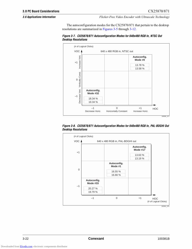
3.0 PC Board Considerations CX25870/871
3.6 Applications Information Flicker-Free Video Encoder with Ultrascale Technology
3-22 Conexant 100381B
The autoconfiguration modes for the CX25870/871 that pertain to the desktop
resolutions are summarized in Figures 3-5 through 3-12.
Figure 3-7. CX25870/871 Autoconfiguration Modes for 640x480 RGB In, NTSC Out Desktop Resolutions
Figure 3-8. CX25870/871 Autoconfiguration Modes for 640x480 RGB In, PAL-BDGHI Out Desktop Resolutions
100381_077
Autoconfig.Mode #0
13.78 %13.58 %
Autoconfig.Mode #32
18.34 %19.34 %
–1
–1
0 HOC
VOC 640 x 480 RGB in, NTSC out
Decrease Horiz.
(# of Logical Clicks)
Increase Horiz.Horizontally Constant
Dec
reas
e V
ert.
Ver
tical
ly C
onst
.In
crea
se V
ert.
0
+1
+1
100381_078
(# of Logical Clicks)
Autoconfig.Mode #17
13.63 %13.19 %
Autoconfig.Mode #1
16.55 %16.66 %
Autoconfig.Mode #33
20.27 %19.79 %
–1
–1
0 HOC
VOC 640 x 480 RGB in, PAL-BDGHI out
(# of Logical Clicks)
0
+1
+1
Downloaded from Elcodis.com electronic components distributor
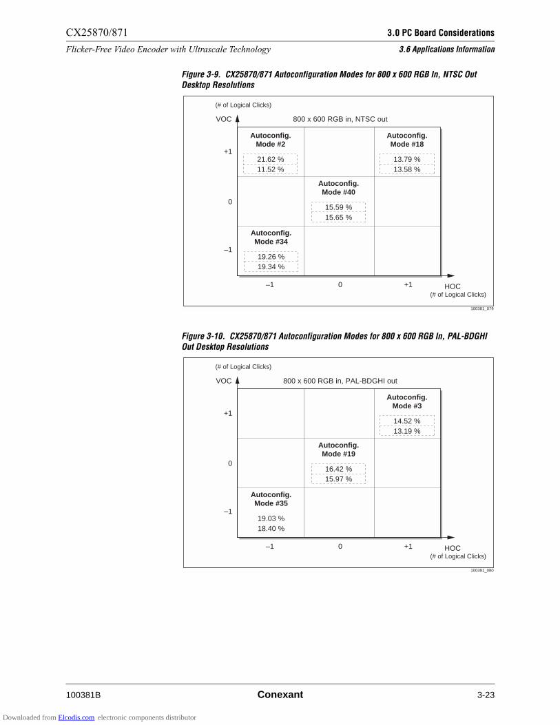
CX25870/871 3.0 PC Board Considerations
Flicker-Free Video Encoder with Ultrascale Technology 3.6 Applications Information
100381B Conexant 3-23
Figure 3-9. CX25870/871 Autoconfiguration Modes for 800 x 600 RGB In, NTSC Out Desktop Resolutions
Figure 3-10. CX25870/871 Autoconfiguration Modes for 800 x 600 RGB In, PAL-BDGHI Out Desktop Resolutions
100381_079
Autoconfig.Mode #18
13.79 %13.58 %
Autoconfig.Mode #2
21.62 %11.52 %
Autoconfig.Mode #40
15.59 %15.65 %
Autoconfig.Mode #34
19.26 %19.34 %
–1
–1
0 HOC
VOC 800 x 600 RGB in, NTSC out
(# of Logical Clicks)
(# of Logical Clicks)
0
+1
+1
100381_080
Autoconfig.Mode #3
14.52 %13.19 %
Autoconfig.Mode #19
16.42 %15.97 %
Autoconfig.Mode #35
19.03 %18.40 %
–1
–1
0 HOC
VOC 800 x 600 RGB in, PAL-BDGHI out
(# of Logical Clicks)
(# of Logical Clicks)
0
+1
+1
Downloaded from Elcodis.com electronic components distributor

3.0 PC Board Considerations CX25870/871
3.6 Applications Information Flicker-Free Video Encoder with Ultrascale Technology
3-24 Conexant 100381B
Figure 3-11. CX25870/871 Autoconfiguration Modes for 1024 x 768 RGB In, NTSC Out Desktop Resolutions
Figure 3-12. CX25870/871 Autoconfiguration Modes for 1024 x 768 RGB In, PAL-BDGHI Out Desktop Resolutions
100381_081
Autoconfig.Mode #26
11.97 %11.93 %
Autoconfig.Mode #10
15.11 %14.81 %
Autoconfig.Mode #42
18.04 %18.11 %
–1
–1
0 HOC
VOC 1024 x 768 RGB in, NTSC out
Decrease Horiz.
(# of Logical Clicks)
Increase Horiz.Horizontally Constant
Dec
reas
e V
ert.
Ver
tical
ly C
onst
.In
crea
se V
ert.
0
+1
+1
100381_082
Autoconfig.Mode #11
13.44 %14.24 %
Autoconfig.Mode #43
16.20 %16.67 %
–1
–1
0 HOC
VOC 1024 x 768 RGB in, PAL-BDGHI out
(# of Logical Clicks)
(# of Logical Clicks)
0
+1
+1
Downloaded from Elcodis.com electronic components distributor

CX25870/871 3.0 PC Board Considerations
Flicker-Free Video Encoder with Ultrascale Technology 3.6 Applications Information
100381B Conexant 3-25
Customers are urged to enable the autoconfiguration mode that is in the
middle of each chart as the default Size for each active resolution. To accomplish
this, the encoder’s CONFIG[5:0] bit field must be programmed to the desired
mode. In addition, the graphics controller’s HTOTAL register must be
programmed to match the CX25870/871’s H_CLKI[10:0] value, and VTOTAL
register must be programmed to match the CX25870/871’s V_LINESI[10:0]
value. Other minor modifications may be necessary. The specific procedure to
follow to enable different overscan ratios is explained in an application note titled
Supporting TV Out with Non-Standard Graphics Input Resolutions. Request this
document from your local Conexant Sales representative for help on the Size
video adjustment.
A simpler alternative to independent horizontal and vertical size buttons is to
replace the directional control pad with a slider. This slider would only have 3 tick
marks and would cycle through the different sizes available based on the
autoconfiguration modes that exist for the specific desktop resolution and video
output type. This concept is illustrated in Figure 3-13.
The slider would alter the horizontal and vertical size of the TV picture
simultaneously by changing the overscan percentages by the same amount. Size
control should only be effective for desktop resolutions such as 640x480,
800x600, and 1024x768. Nonstandard resolutions should choose a single size
with a moderate amount of overscan compensation (HOC/VOC = 11 percent–16
percent) and not allow the end-user to deviate from this choice by graying out the
Size slider.
Figure 3-13. Direction-less Size Control Pad
Downloaded from Elcodis.com electronic components distributor
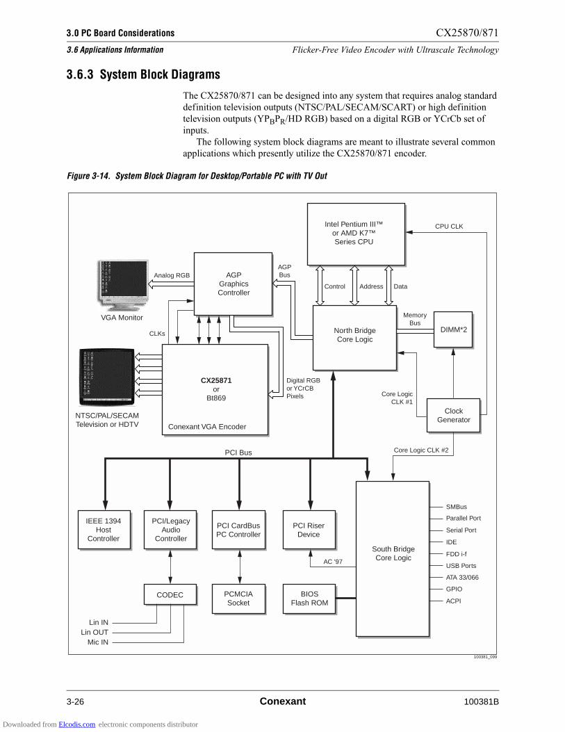
3.0 PC Board Considerations CX25870/871
3.6 Applications Information Flicker-Free Video Encoder with Ultrascale Technology
3-26 Conexant 100381B
3.6.3 System Block Diagrams
The CX25870/871 can be designed into any system that requires analog standard
definition television outputs (NTSC/PAL/SECAM/SCART) or high definition
television outputs (YPBPR/HD RGB) based on a digital RGB or YCrCb set of
inputs.
The following system block diagrams are meant to illustrate several common
applications which presently utilize the CX25870/871 encoder.
Figure 3-14. System Block Diagram for Desktop/Portable PC with TV Out
100381_099
Intel Pentium III™or AMD K7™Series CPU
AGPGraphicsController
CX25871or
Bt869
North BridgeCore Logic
DIMM*2
CPU CLK
MemoryBus
AC '97
AGPBus
Digital RGBor YCrCBPixels
SMBus
Parallel Port
Serial Port
IDE
FDD i-f
USB Ports
ATA 33/066
GPIO
ACPI
Core LogicCLK #1
Lin INLin OUT
Mic IN
CLKs
Core Logic CLK #2
Analog RGB
Control Address Data
CODEC
VGA Monitor
NTSC/PAL/SECAMTelevision or HDTV
ClockGenerator
IEEE 1394Host
Controller
PCI/LegacyAudio
Controller
PCI CardBusPC Controller
PCMCIASocket
BIOSFlash ROM
South BridgeCore Logic
PCI RiserDevice
PCI Bus
Conexant VGA Encoder
Downloaded from Elcodis.com electronic components distributor

CX25870/871 3.0 PC Board Considerations
Flicker-Free Video Encoder with Ultrascale Technology 3.6 Applications Information
100381B Conexant 3-27
3.6.4 Electrostatic Discharge and Latchup Considerations
Correct electrostatic discharge (ESD)-sensitive handling procedures are required
to prevent device damage. Device damage can produce symptoms of catastrophic
failure or erratic device behavior with leaky inputs.
All logic inputs should be held low until power to the device has settled to the
specified tolerance. DAC power decoupling networks with large time constants
should be avoided; they could delay VAA and VDD power to the device. Ferrite
beads must be used only for analog power VAA decoupling. Inductors cause a
time-constant delay that induces latchup, and should not be substituted for a
ferrite bead.
Latchup can be prevented by ensuring that all VAA and VDD pins are at the
same potential and by forcing all AGND and VSS pins to be at the same potential.
The VAA and VDD supply voltage must be applied before the signal pin voltages.
The correct power-up sequence ensures that any signal pin voltage will never
exceed the power supply voltage.
Figure 3-15. System Block Diagram for Graphics Card with TV Out
100381_100
AGPGraphicsController
AGP Bus
Analog RGB
AnalogRGB
DACOutputs
CLKsSYNC*sandBLANK*
Digital RGBorYCrCB Pixels
CX25871or
Bt869
VGA Monitor
NTSC/PAL/SECAMTelevision or HDTV
SGRAM*8or SDRAM*8
VoltageRegulator
GraphicsBIOS
Flash ROM
Conexant VGA Encoder
Downloaded from Elcodis.com electronic components distributor
3.0 PC Board Considerations CX25870/871
3.6 Applications Information Flicker-Free Video Encoder with Ultrascale Technology
3-28 Conexant 100381B
3.6.5 Clock and Subcarrier Stability
The color subcarrier frequency is derived directly from the XTALIN/XTALOUT
ports when EN_XCLK=0. The color subcarrier frequency is derived directly from
the main clock input, CLKI, when EN_XCLK=1 (slave interface). In either case
any jitter or frequency deviation from 13.500 MHz (XTALIN/XTALOUT) or the
CLKI (slave interface) rate will be transferred directly to the color subcarrier.
Jitter within the valid clock cycle interval will result in hue noise on the color
subcarrier on the order of 0.9–1.6 degrees per nanosecond. Random hue noise can
result in degradation in the AM/PM noise ratio (typically around 40 dB for
consumer media such as Videodiscs and VCRs). Periodic or coherent hue noise
can result in differential phase error (which is limited to 10 degrees by FCC cable
TV standards).
Any frequency deviation of CLKI from the transmitted clock (i.e., CLKO)
will challenge the subcarrier tracking capability of the destination receiver. This
may range from a few parts-per-million (ppm) for broadcast equipment, to 100
ppm for industrial equipment and to >100 ppm for consumer equipment. Greater
subcarrier tracking range generally results in poorer subcarrier decoding dynamic
range. So, receivers that tolerate jitter and wide subcarrier frequency deviation
will introduce more noise in the decoded image. Crystal-based clock sources with
a maximum total deviation of 50 ppm (NTSC) or 25 ppm (PAL, SECAM) across
the temperature range of 0 °C to 70 °C produce the best results for consumer and
industrial applications. In rare cases, temperature-compensated clock sources
with tighter tolerances may be warranted for broadcast or more stringent PAL
(e.g., type I) applications.
Some applications call for maintaining correct Subcarrier-Horizontal (SC-H)
phasing for correct color framing. This requires subcarrier coherence within
specified tolerances over a four-field interval for 525-line systems or 8 fields for
625-line systems. Any clock interruption (even during vertical blanking interval)
which results in mis-registration of the CLKI input or nonstandard pixel counts
per line, can result in SC-H excursions outside the NTSC limit of ±40 degrees
(reference EIA RS170A) or the PAL limit of ±20 degrees (reference EBU
D23-1984).
In slave interface, any deviation exceeding the 50 ppm (NTSC) or 25 ppm
(PAL, SECAM) limits of the number clock cycles between HSYNC* falling
edges may result in a switch to Master Mode.
A list of recommended crystals and crystal vendors is contained in
Appendix B.
Downloaded from Elcodis.com electronic components distributor
CX25870/871 3.0 PC Board Considerations
Flicker-Free Video Encoder with Ultrascale Technology 3.6 Applications Information
100381B Conexant 3-29
3.6.6 Filtering Radio Frequency Modulator Connection
The CX25870/871 internal upsampling filter alleviates external filtering
requirements by moving significant sampling alias components above 19 MHz
and reducing the sinx/x aperture loss up to the filter’s passband cutoff of
5.75 MHz. While typical chrominance subcarrier decoders can handle the
CX25870/871 output signals without analog filtering, the higher frequency alias
products pose some EMI concerns and may create troublesome images when
introduced to a radio frequency (RF) modulator. When the video is presented to
an RF modulator, it should be free of energy in the region of the aural subcarrier
(4.5 MHz for NTSC, 5.5–6.5 MHz for PAL). Hence some additional frequency
traps may be necessary when the video signal contains fundamental or harmonic
energy (as from unfiltered character generators) in that region. Where better
frequency response flatness is required, some peaking in the analog filter is
appropriate to compensate for residual digital filter losses with sufficient margin
to tolerate 10 percent reactive components.
A three-pole elliptic filter (one inductor, three capacitors) with a 6.75 MHz
passband can provide at least 45 dB attenuation (including sinx/x loss) of
frequency components above 20 MHz and provide some flexibility for mild
peaking or special traps. An inductor value with a self-resonant frequency above
80 MHz is chosen so that its intrinsic capacitance contributes less than 10 percent
of the total effective circuit value. The inductor itself may induce 1 percent
(0.1 dB) loss. Any additional ferrites introduced for EMI control should have less
than 5 " impedance below 5 MHz to minimize additional losses. The capacitor to
ground at the CX25870/871 output pin is compensating for the parasitic
capacitance of the chip plus any protection diodes and lumped circuit traces
(about 22 pF + 5 pF/diode). Some filter peaking can be accomplished by splitting
the 75 " source impedance across the reactive PI filter network. However, this
will also introduce some chrominance-luminance delay distortion in the range of
10–20 ns for a maximum of 0.5 dB boost at the subcarrier frequency.
The filter network feeding an RF modulator may include the aforementioned
trap, which could take two forms depending on the depth of attenuation and type
of resonator device employed.
The trap circuitry can interact with the low-pass filter, compromising
frequency response flatness. A simple PNP buffer can preserve the benefits of an
oversampling encoder when simultaneous Composite Video Baseband Signals
(CVBS) are required for driving external cables. In addition, an active video
buffer, serves to isolate the RF modulator signal amplitude from anomalies in the
external termination. This buffer can be implemented with a transistor array or
video amplify IC which provides a gain of two (before series termination),
capable of driving 740 µA into the 75 " destination, and is biased within its
input/output compliance range. When simultaneous Y/C (s-video) outputs are not
required, a second CVBS signal can be created (with a 600 mV sync to tip offset)
by tying these pins together with a single termination resistor (typically 75 ") and
driving the low-pass filter circuit.
The RF modulator typically has a high input impedance (about 1 k " ±30
percent) and loose tolerance. Consequently, the amplitude variation at the
modulator input will be greater, especially when the trap is properly terminated at
the modulator input for maximum effect. Some modulators, video or aural
fidelity, degrade dramatically when overdriven, so the value of the effective
termination (nominally 37.5 ") may need to be adjusted downward to maintain
sufficient linearity (or depth of modulation margin) in the RF signal.
Downloaded from Elcodis.com electronic components distributor
3.0 PC Board Considerations CX25870/871
3.6 Applications Information Flicker-Free Video Encoder with Ultrascale Technology
3-30 Conexant 100381B
A two-section trap (with associated inductor) may be warranted to achieve
better than 20 dB attenuation when stereo, SAP, or AM aural carriers are
generated, or when >40 dB audio dynamic range is desired. Some impedance
isolation (e.g., buffer) may be required before the trap to obtain the flattest
frequency response.
Downloaded from Elcodis.com electronic components distributor
CX25870/871 3.0 PC Board Considerations
Flicker-Free Video Encoder with Ultrascale Technology 3.7 CX870EVK Evaluation Kit
100381B Conexant 3-31
3.7 CX870EVK Evaluation Kit
A new reference design kit is available now to facilitate implementation of
Conexant’s VGA encoder into a graphics subsystem. This kit is called the
GeForce2 MX-400 CX870EVK and can be obtained through your local Conexant
Systems sales office.
The new CX25870 Evaluation Kit uses the NVidia P36 model reference
design AGP card, containing the popular NVidia GeForce2 MX-400™
graphics-processing unit (GPU), as a high-performance data master to provide
digital data to the CX25870 PC video encoder. The Conexant device has been
mounted directly on this graphics card along with all necessary passive
components (resistors, capacitors, inductors, video connectors, etc.) to ensure
proper device operation. This two-chip combination is controlled by a set of
drivers for the graphics accelerator written by NVidia and a separate Windows
program called Super Cockpit created by Conexant that allows direct
manipulation of the encoder device by circumventing the driver software. All the
necessary documents and cables have been within the kit as well. The
multipronged DV-H cable from JIC USA is included with the kit and will be
necessary for viewing of HDTV, 480i Component Video Out, S-Video,
Composite, and any other TV output from the CX25870 encoder.
To obtain the necessary CX870EVK software, find a PC with Internet access
and visit the CX25870 https://site. For the site address, username, and password,
contact your local Conexant Systems sales office. Once you have been given user
identification information, you can download the GeForce2 MX-400 CX870EVK
instruction manual, Super Cockpit, test images, and other pertinent software.
The CX870EVK was designed to be both a demonstration unit and
development unit depending on a customer’s needs. For demonstration purposes,
many script files have been created and will be automatically extracted and
placed into a /ScriptFiles subdirectory under the CX870EVK’s main directory. To
execute a script file, launch a DOS-BOX, type the desired script filename
(without the extension) on the command line, and then press the <ENTER> key.
After execution, the script file will have configured both the CX25870 encoder
and the GeForce2 MX-400 graphics controller to a specific mode in terms of
resolution and video output. This is the most effective method for achieving the
optimal TV Out picture quickly.
For development purposes, several new pages have been added to Super
Cockput including the handy Clipboard pages which allow the end-user to try out
register values and restore them if the result is not desirable. All registers can be
read from as well—an improvement over the Bt868/9. Write access to all the new
bits and registers found within the CX25870 are also possible. Note that the
GeForce2 MX-400 controller supports the CX25870 in a pseudo-master
interface. As a result, HDTV YPRPB Output is possible with the GeForce2
MX-400 CX870EVK kit.
Downloaded from Elcodis.com electronic components distributor
3.0 PC Board Considerations CX25870/871
3.7 CX870EVK Evaluation Kit Flicker-Free Video Encoder with Ultrascale Technology
3-32 Conexant 100381B
In addition, the ability to switch between the most popular desktop resolutions
(640x480, 800x600, and 1024x768) and video output types
(NTSC/PAL/SECAM) is much simpler now than with the original Bt868EVK.
Finally, sliders commonly found on TV Out Display Properties pages such as
brightness, contrast, saturation, flicker filtering and hue have been integrated into
the Super Cockpit application itself on the Display page. Users are encouraged to
manipulate these controls to achieve their desired TV outputs and save the
encoder settings for future usage.
Downloaded from Elcodis.com electronic components distributor

CX25870/871 3.0 PC Board Considerations
Flicker-Free Video Encoder with Ultrascale Technology 3.8 Serial Interface
100381B Conexant 3-33
3.8 Serial Interface
3.8.1 Data Transfer on the Serial Interface Bus
Figure 3-16 illustrates the relationship between SID (Serial Interface Data) and
SIC (Serial Interface Clock) to be used when programming the internal registers
via the Serial Interface bus. If the bus is not being used, both SID and SIC lines
must be left high.
Every byte put onto the SID line should be 8 bits long (MSB first), followed
by an acknowledge bit, which is generated by the receiving device. Each data
transfer is initiated with a start condition and ended with a stop condition. The
first byte after a start condition is always the slave device address byte. If this is
the device’s own address, the device will generate an acknowledge by pulling the
SID line low during the ninth clock pulse, then accept the data in subsequent
bytes (auto-incrementing the subaddress) until another stop condition is detected.
The eighth bit of the address byte is the read/write bit (high = read from
addressed device; low = write to the addressed device). Data bytes are always
acknowledged during the ninth clock pulse by the addressed device.
NOTE: During the acknowledge period, the transmitting device must leave the SID
line high.
Premature termination of the data transfer is allowed by generating a stop
condition at any time. When this happens, the CX25870/871 will remain in the
state defined by the last complete data byte transmitted and any master
acknowledge subsequent to reading the chip ID (subaddress 0x89 if ALTADDR
pin is 0) is ignored.
The maximum serial interface speed for the CX25870/871 is 400 kHz.
Downloaded from Elcodis.com electronic components distributor
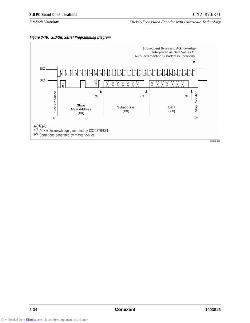
3.0 PC Board Considerations CX25870/871
3.8 Serial Interface Flicker-Free Video Encoder with Ultrascale Technology
3-34 Conexant 100381B
Figure 3-16. SID/SIC Serial Programming Diagram
1
SIC
2 3 4 5 6 7 8 9 1 2 3 4 5 6 7 8 9 1 2 3 4 5 6 7 8 9
Subsequent Bytes and AcknowledgeInterpreted as Data Values for
Auto-Incrementing Subaddress Locations
SID
MS
B
LSB
(1)
(2) (2)
Sta
rt C
ondi
tion
Sto
p C
ondi
tion
Subaddress(XX)
Data(XX)
(1) (1)
SlaveMain Address
(XX)
100381_021
NOTE(S):(1) ACK = Acknowledge generated by CX25870/871.(2) Conditions generated by master device.
Downloaded from Elcodis.com electronic components distributor
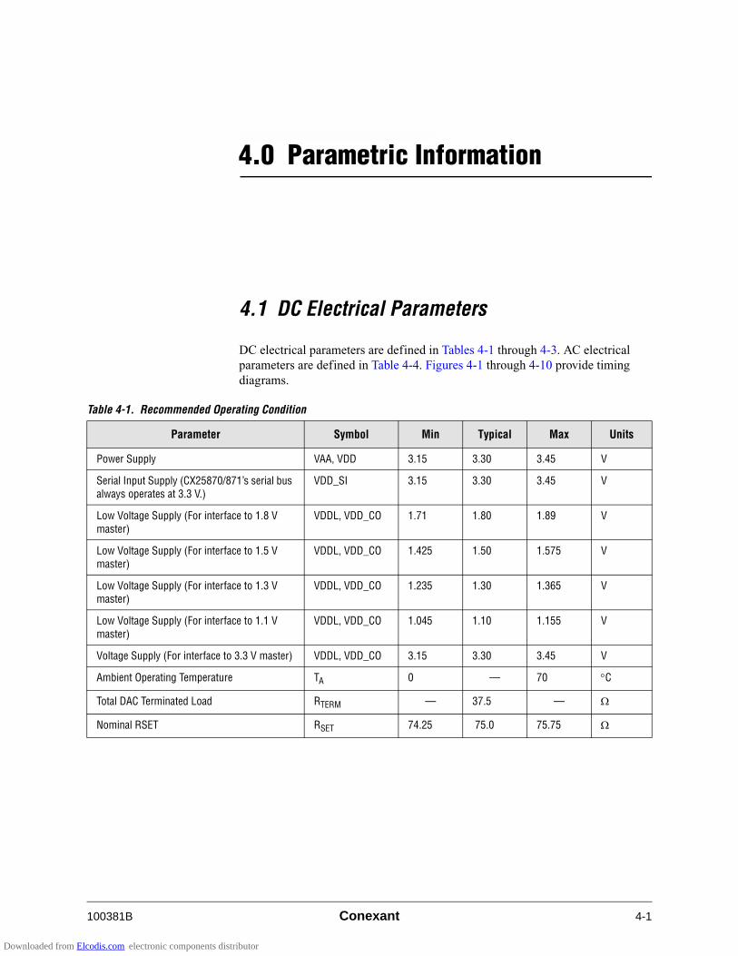
100381B Conexant 4-1
4
4.0 Parametric Information
4.1 DC Electrical Parameters
DC electrical parameters are defined in Tables 4-1 through 4-3. AC electrical
parameters are defined in Table 4-4. Figures 4-1 through 4-10 provide timing
diagrams.
Table 4-1. Recommended Operating Condition
Parameter Symbol Min Typical Max Units
Power Supply VAA, VDD 3.15 3.30 3.45 V
Serial Input Supply (CX25870/871’s serial bus always operates at 3.3 V.)
VDD_SI 3.15 3.30 3.45 V
Low Voltage Supply (For interface to 1.8 V
master)
VDDL, VDD_CO 1.71 1.80 1.89 V
Low Voltage Supply (For interface to 1.5 V master)
VDDL, VDD_CO 1.425 1.50 1.575 V
Low Voltage Supply (For interface to 1.3 V master)
VDDL, VDD_CO 1.235 1.30 1.365 V
Low Voltage Supply (For interface to 1.1 V
master)
VDDL, VDD_CO 1.045 1.10 1.155 V
Voltage Supply (For interface to 3.3 V master) VDDL, VDD_CO 3.15 3.30 3.45 V
Ambient Operating Temperature TA 0 — 70 'C
Total DAC Terminated Load RTERM — 37.5 — "
Nominal RSET RSET 74.25 75.0 75.75 "
Downloaded from Elcodis.com electronic components distributor
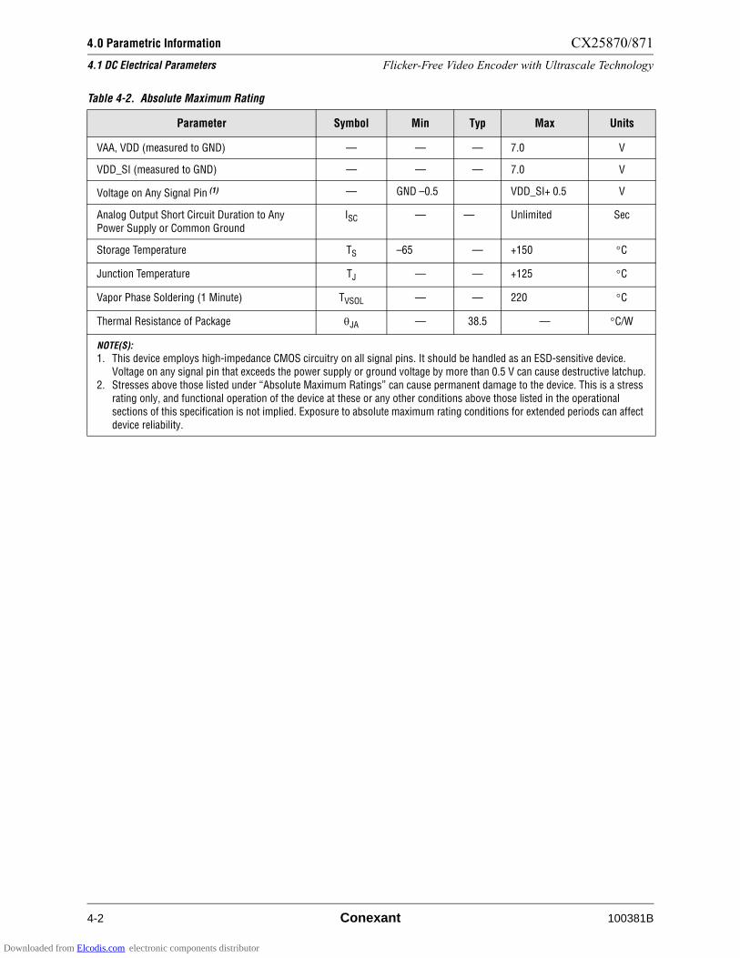
4.0 Parametric Information CX25870/871
4.1 DC Electrical Parameters Flicker-Free Video Encoder with Ultrascale Technology
4-2 Conexant 100381B
Table 4-2. Absolute Maximum Rating
Parameter Symbol Min Typ Max Units
VAA, VDD (measured to GND) — — — 7.0 V
VDD_SI (measured to GND) — — — 7.0 V
Voltage on Any Signal Pin (1) — GND –0.5 VDD_SI+ 0.5 V
Analog Output Short Circuit Duration to Any
Power Supply or Common Ground
ISC — — Unlimited Sec
Storage Temperature TS –65 — +150 'C
Junction Temperature TJ — — +125 'C
Vapor Phase Soldering (1 Minute) TVSOL — — 220 'C
Thermal Resistance of Package (JA — 38.5 — 'C/W
NOTE(S):
1. This device employs high-impedance CMOS circuitry on all signal pins. It should be handled as an ESD-sensitive device. Voltage on any signal pin that exceeds the power supply or ground voltage by more than 0.5 V can cause destructive latchup.
2. Stresses above those listed under “Absolute Maximum Ratings” can cause permanent damage to the device. This is a stress rating only, and functional operation of the device at these or any other conditions above those listed in the operational sections of this specification is not implied. Exposure to absolute maximum rating conditions for extended periods can affect
device reliability.
Downloaded from Elcodis.com electronic components distributor
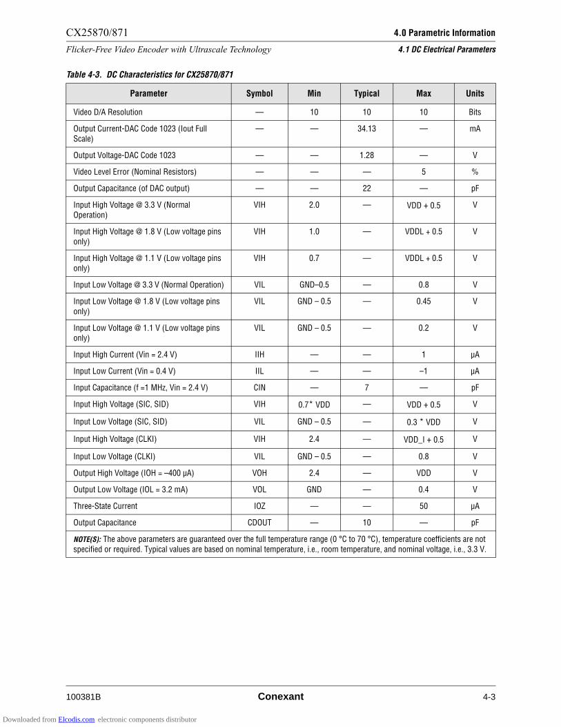
CX25870/871 4.0 Parametric Information
Flicker-Free Video Encoder with Ultrascale Technology 4.1 DC Electrical Parameters
100381B Conexant 4-3
Table 4-3. DC Characteristics for CX25870/871
Parameter Symbol Min Typical Max Units
Video D/A Resolution — 10 10 10 Bits
Output Current-DAC Code 1023 (Iout Full Scale)
— — 34.13 — mA
Output Voltage-DAC Code 1023 — — 1.28 — V
Video Level Error (Nominal Resistors) — — — 5 %
Output Capacitance (of DAC output) — — 22 — pF
Input High Voltage @ 3.3 V (Normal
Operation)
VIH 2.0 — VDD + 0.5 V
Input High Voltage @ 1.8 V (Low voltage pins only)
VIH 1.0 — VDDL + 0.5 V
Input High Voltage @ 1.1 V (Low voltage pins only)
VIH 0.7 — VDDL + 0.5 V
Input Low Voltage @ 3.3 V (Normal Operation) VIL GND–0.5 — 0.8 V
Input Low Voltage @ 1.8 V (Low voltage pins
only)
VIL GND – 0.5 — 0.45 V
Input Low Voltage @ 1.1 V (Low voltage pins only)
VIL GND – 0.5 — 0.2 V
Input High Current (Vin = 2.4 V) IIH — — 1 µA
Input Low Current (Vin = 0.4 V) IIL — — –1 µA
Input Capacitance (f =1 MHz, Vin = 2.4 V) CIN — 7 — pF
Input High Voltage (SIC, SID) VIH 0.7* VDD — VDD + 0.5 V
Input Low Voltage (SIC, SID) VIL GND – 0.5 — 0.3 * VDD V
Input High Voltage (CLKI) VIH 2.4 — VDD_I + 0.5 V
Input Low Voltage (CLKI) VIL GND – 0.5 — 0.8 V
Output High Voltage (IOH = –400 µA) VOH 2.4 — VDD V
Output Low Voltage (IOL = 3.2 mA) VOL GND — 0.4 V
Three-State Current IOZ — — 50 µA
Output Capacitance CDOUT — 10 — pF
NOTE(S): The above parameters are guaranteed over the full temperature range (0 °C to 70 °C), temperature coefficients are not
specified or required. Typical values are based on nominal temperature, i.e., room temperature, and nominal voltage, i.e., 3.3 V.
Downloaded from Elcodis.com electronic components distributor
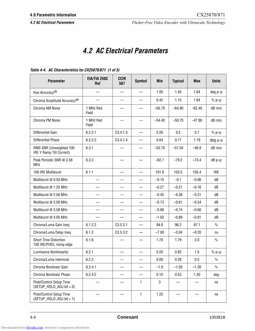
4.0 Parametric Information CX25870/871
4.2 AC Electrical Parameters Flicker-Free Video Encoder with Ultrascale Technology
4-4 Conexant 100381B
4.2 AC Electrical Parameters
Table 4-4. AC Characteristics for CX25870/871 (1 of 3)
ParameterEIA/TIA 250C
RefCCIR 567
Symbol Min Typical Max Units
Hue Accuracy(2) — — — 1.05 1.45 1.64 deg p–p
Chroma Amplitude Accuracy(2) — — — 0.42 1.15 1.64 % p–p
Chroma AM Noise 1 MHz Red Field
— — –65.70 –64.90 –62.40 dB rms
Chroma PM Noise 1 MHz Red Field
— — –54.40 –50.70 –47.90 dB rms
Differential Gain 6.2.2.1 C3.4.1.3 — 0.26 0.5 0.7 % p–p
Differential Phase 6.2.2.2 C3.4.1.4 — 0.64 0.71 1.19 deg p–p
RMS SNR (Unweighted 100 IRE Y Ramp Tilt Correct)
6.3.1 — — –53.70 –51.04 –46.9 dB rms
Peak Periodic SNR @ 3.58
MHz
6.3.2 — — –82.7 –79.2 –73.4 dB p–p
100 IRE Multiburst 6.1.1 — — 101.9 103.5 105.4 IRE
Multiburst @ 0.50 MHz — — — –0.15 –0.1 –0.06 dB
Multiburst @ 1.25 MHz — — — –0.27 –0.21 –0.16 dB
Multiburst @ 2.00 MHz — — — –0.45 –0.36 –0.31 dB
Multiburst @ 3.00 MHz — — — –0.73 –0.61 –0.54 dB
Multiburst @ 3.58 MHz — — — –0.88 –0.74 –0.66 dB
Multiburst @ 4.05 MHz — — — –1.03 –0.89 –0.81 dB
Chroma/Luma Gain Ineq 6.1.2.2 C3.5.3.1 — 94.8 96.2 97.1 %
Chroma/Luma Delay Ineq 6.1.2 C3.5.3.2 — –7.00 –3.04 –0.20 ns
Short Time Distortion 100 IRE/PIXEL rising edge
6.1.6 — — 1.70 1.79 2.0 %
Luminance Nonlinearity 6.2.1 — — 0.20 0.82 1.5 % p–p
Chroma/Luma Intermod 6.2.3 — — 0.00 0.28 0.5 %
Chroma Nonlinear Gain 6.2.4.1 — — –1.9 –1.59 –1.30 %
Chroma Nonlinear Phase 6.2.4.2 — — 0.10 0.53 1.30 deg
Pixel/Control Setup Time
(SETUP_HOLD_ADJ bit = 0)
— — 1 3 — — ns
Pixel/Control Setup Time (SETUP_HOLD_ADJ bit = 1)
— — 1 1.25 — — ns
Downloaded from Elcodis.com electronic components distributor

CX25870/871 4.0 Parametric Information
Flicker-Free Video Encoder with Ultrascale Technology 4.2 AC Electrical Parameters
100381B Conexant 4-5
ParameterEIA/TIA 250C
RefCCIR 567
Symbol Min Typical Max Units
Pixel/Control Hold Time
(SETUP_HOLD_ADJ bit = 0)
— — 2 0 — — ns
Pixel/Control Hold Time (SETUP_HOLD_ADJ bit = 1)
— — 2 1.5 — — ns
Control Output Delay Time(4) — — 3 — — 10.0 ns
Control Output Hold Time(4) — — 4 2 — ns
CLKI/O Frequency (standard
mode)
— — — — — 53.3333
MHz
CLKI/O Pulse Width Low Duty
Cycle(3)
— — — 40 50 60 %
CLKI/O Pulse Width High Duty
Cycle(3)
— — — 40 50 60 %
CLKO to CLKI Delay — — 7 — — 0.8 CLKO cycles
SLAVE to HSYNC*/VSYNC*
Three-state(3)
— — 5 2 — — CLKI
cycles
SLAVE to HSYNC*/VSYNC*
Active(3)
— — 6 — — 2 CLKI cycles
VAA Supply Current (minimum
3 DACS on)(8)
— — — — 190 — mA
VDD Supply Current
(minimum 3 DACS on)(8)
— — — — 220 — mA
Total Supply Current
(minimum 3 DACS on)(8)
— — — — 410 — mA
Power-Down Current — — — — 3(7) — mA
Power-Down Current (need a Hardware RESET to bring the
part up)
— — — — 1.5(6) — mA
Table 4-4. AC Characteristics for CX25870/871 (2 of 3)
Downloaded from Elcodis.com electronic components distributor

4.0 Parametric Information CX25870/871
4.2 AC Electrical Parameters Flicker-Free Video Encoder with Ultrascale Technology
4-6 Conexant 100381B
HDTV Output Timing Characteristics: 1080i (see Figure 4-9)
Parameter Symbol Min Typical Max Units
Lowsync width ) — 598.8 — ns
Start of line to end of active video * — 28.385 — !s
Highsync width + — 598.8 — ns
Rising edge of sync to start of broad pulse , — 1.796 — !s
Start of line to start of active video - — 2.588 — !s
Sync rise time . — 54.5 — ns
Total line time — — 29.685 — !s
Active line time — — 25.778 — !s
HDTV Output Timing Characteristics: 720p (see Figure 4-10)
Parameter Symbol Min Typical Max Units
Lowsync width a — 548 — ns
Start of line to end of active video b — 20.54 — !s
High sync width c — 548 — ns
Rising edge of sync to start of broad pulse d — 3.53 — !s
Rising edge of sync to start of active video e — 3.53 — !s
Sync rise time — — 54.7 — ns
Total line time — — 22.2 — !s
Active line time — — 17.16 — !s
NOTE(S):
1. Guaranteed by characterization; NTSC output, no vertical or horizontal scaling. Flicker Filter and other internal low-pass filters
bypassed, and contrast, brightness, saturation levels set to full scale.(2) 100/7.5/100/7.5 Color bars normalized to burst.(3) Guaranteed by design.(4) Control pins are defined as: BLANK*, HSYNC*, VSYNC*, FIELD, CLKO, CLKI, RESET*, PAL, and SLAVE.(5) DAC output load < 75 pF. HSYNC*, VSYNC*, BLANK*, and FIELD output load < 75 pF. As the above parameters are
guaranteed over the full temperature range, temperature coefficients are not specified or required. Typical values are based on nominal temperature, i.e., room temperature, and nominal voltage, i.e., 3.3 V.
(6) There are numerous power-down options. This value was determined by setting SLEEP_EN, DIS_CLKI, DIS_CLKO, BY_PLL,
XTL_BFO_DIS, XTAL_PAD_DIS bits and pulling the SLEEP pin high.(7) This value was determined by setting BY_PLL, SLEEP_ED, DIS_CLKI, DIS_CLKO, XTAL_BFO_DIS bits.(8) To ensure that the encoder performance falls within DC and AC electrical limits, no more than one DAC should be disabled at
any time.
Table 4-4. AC Characteristics for CX25870/871 (3 of 3)
Downloaded from Elcodis.com electronic components distributor
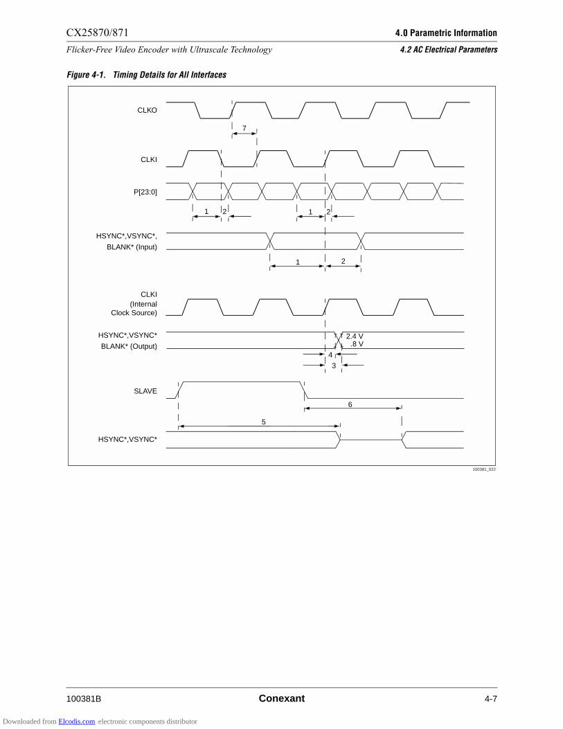
CX25870/871 4.0 Parametric Information
Flicker-Free Video Encoder with Ultrascale Technology 4.2 AC Electrical Parameters
100381B Conexant 4-7
Figure 4-1. Timing Details for All Interfaces
CLKI
P[23:0]
HSYNC*,VSYNC*
1 2
3
4
.8 V2.4 V
BLANK* (Output)
HSYNC*,VSYNC*,
BLANK* (Input)
5
SLAVE
1 2
1 2
HSYNC*,VSYNC*
6
(InternalCLKI
Clock Source)
CLKO
7
100381_022
Downloaded from Elcodis.com electronic components distributor
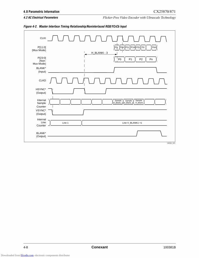
4.0 Parametric Information CX25870/871
4.2 AC Electrical Parameters Flicker-Free Video Encoder with Ultrascale Technology
4-8 Conexant 100381B
Figure 4-2. Master Interface Timing Relationship/Noninterlaced RGB/YCrCb Input
InternalSample
VSYNC*(Output)
CLKI
HSYNC*(Output)
P[11:0]
BLANK*(Input)
BLANK*(Output)
(Mux Mode)
P[23:0](Non-
CLKO
InternalLine
Counter
H_BLANKI - 3
Mux Mode)
Counter
SampleH_Blank_1
SampleH_Blank_2
SampleH_Blank
Line 1 Line V_BLANK1 +1
POL POH P1L P1H P2L PnH
P0 P1 P2 Pn
P2H
100381_023
Downloaded from Elcodis.com electronic components distributor
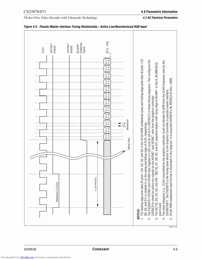
CX25870/871 4.0 Parametric Information
Flicker-Free Video Encoder with Ultrascale Technology 4.2 AC Electrical Parameters
100381B Conexant 4-9
Figure 4-3. Pseudo-Master Interface Timing Relationship – Active Line/Noninterlaced RGB Input
. .
100381_058
Min
imum
2 C
LKs
H_B
LAN
KI[9
:0]
R7-
0G
-loR
7-0
G-lo
B7-
0G
-up
B7-
0G
-up
R7-
0G
-loB
7-0
G-u
pR
7-0
G-lo
B7-
0G
-up
R7-
0G
-loB
7-0
G-u
pR
7-0
G-lo
CLK
I
VS
YN
C*
(Inp
ut)
BLA
NK
*(O
ptio
nal
Inpu
t)
[P11
- P
0]
HS
YN
C*
(Inp
ut)
B7-
0G
-up
Man
y cl
ks
3 ns
.M
inim
um
NO
TE(S
):1
. T
he
lead
ing
ed
ge
pix
el d
ata
(R p
ixel
+ G
4,
G3
, G
2,
and
G0
in t
he
24
-bit
RG
B m
ult
iple
xed
cas
e) a
nd
tra
ilin
g e
dg
e p
ixel
dat
a (B
pix
el +
G7
,
G
6,
G5
, an
d G
1)
is c
lock
ed in
on
th
e ri
sin
g a
nd
fal
ling
ed
ge
of
CL
KI,
res
pec
tive
ly.
2.
Th
e C
X2
58
70
's H
SY
NC
I an
d V
SY
NC
I b
its
(reg
iste
r 0
x C
6)
mu
st b
e se
t to
0 (
=D
EFA
UL
T)
in t
hes
e ti
min
g d
iag
ram
s. T
his
co
nfi
gu
res
the
CX
25
87
0 t
o c
hec
k fo
r ac
tive
low
sig
nal
s o
n t
he
HS
YN
C*
an
d V
SY
NC
* p
ins
fro
m t
he
gra
ph
ics
con
tro
ller.
3.
Th
e R
[7:0
], G
4,
G3
, G
2,
and
G0
-
B[7
:0],
G7
, G
6,
G5
, an
d G
1
seq
uen
ce b
egin
s w
ith
ris
ing
ed
ge
of
BL
AN
K*
or
the
H_
BL
AN
KI[
9:0
]
p
ixel
co
un
t.4
. T
he
clo
ck f
req
uen
cy (
i.e.,
CL
KI)
tra
nsm
itte
d b
y th
e g
rap
hic
s co
ntr
olle
r m
ust
no
t d
evia
te 2
5 p
PM
fro
m t
he
CL
KO
fre
qu
ency
sen
t b
y th
e
C
X2
58
70
/87
1.
Th
e C
X2
58
70
is t
he
tim
ing
sla
ve d
evic
e to
th
e G
rap
hic
s C
on
tro
ller
in p
seu
do
-mas
ter
inte
rfac
e.5
. 2
4-b
it R
GB
mu
ltip
lexe
d in
pu
t fo
rmat
is il
lust
rate
d in
th
is d
iag
ram
. It
is a
ssu
med
CX
25
87
0's
IN
_M
OD
E[3
:0]
bit
s =
00
00
.
Downloaded from Elcodis.com electronic components distributor
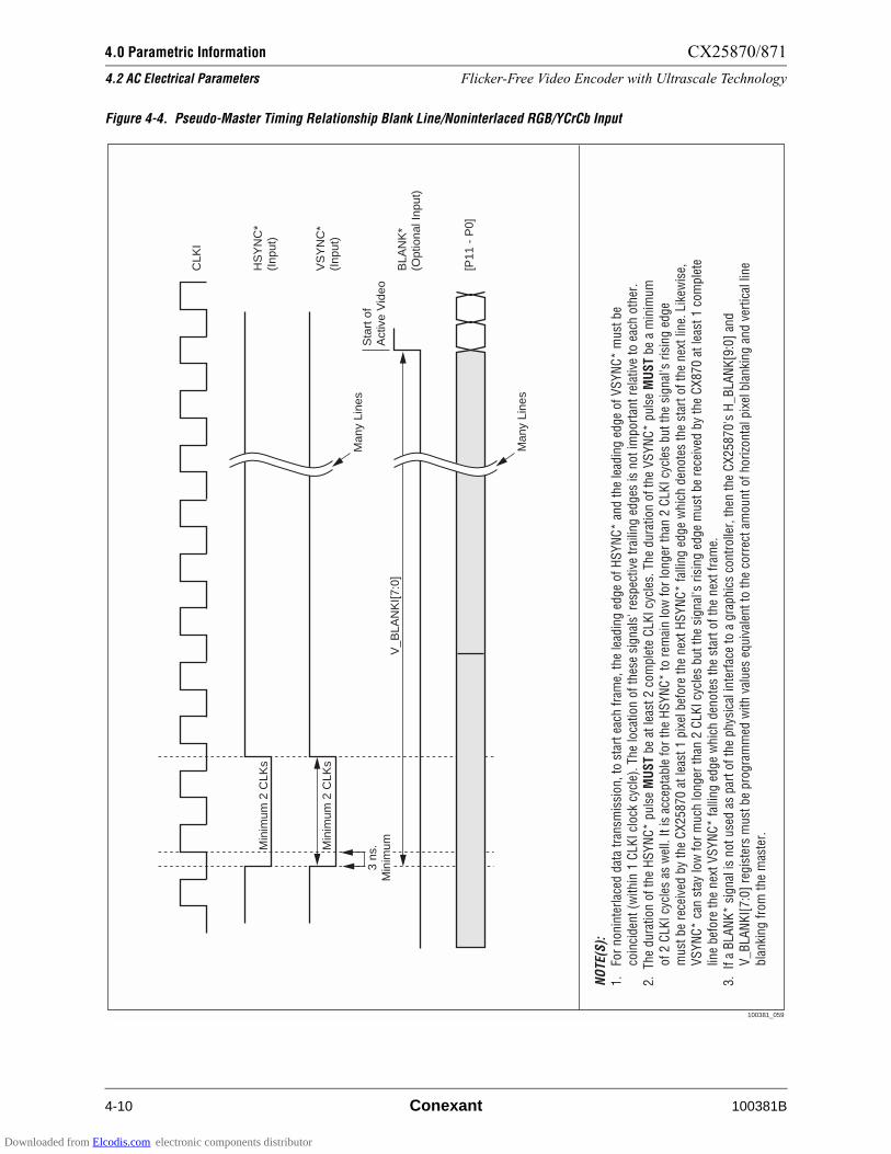
4.0 Parametric Information CX25870/871
4.2 AC Electrical Parameters Flicker-Free Video Encoder with Ultrascale Technology
4-10 Conexant 100381B
Figure 4-4. Pseudo-Master Timing Relationship Blank Line/Noninterlaced RGB/YCrCb Input
100381_059
Min
imum
2 C
LKs
Min
imum
2 C
LKs
V_B
LAN
KI[7
:0]
Man
y Li
nes
Man
y Li
nes
3 ns
.M
inim
um
Sta
rt o
fA
ctiv
e V
ideo
CLK
I
HS
YN
C*
(Inp
ut)
VS
YN
C*
(Inp
ut)
BLA
NK
*(O
ptio
nal I
nput
)
[P11
- P
0]
NO
TE(S
):1
.
For
no
nin
terl
aced
dat
a tr
ansm
issi
on
, to
sta
rt e
ach
fra
me,
th
e le
adin
g e
dg
e o
f H
SY
NC
* a
nd
th
e le
adin
g e
dg
e o
f V
SY
NC
* m
ust
be
co
inci
den
t (w
ith
in 1
CL
KI
clo
ck c
ycle
). T
he
loca
tio
n o
f th
ese
sig
nal
s' r
esp
ecti
ve t
raili
ng
ed
ges
is n
ot
imp
ort
ant
rela
tive
to
eac
h o
ther
.2
. T
he
du
rati
on
of
the
HS
YN
C*
pu
lse
MU
ST b
e at
leas
t 2
co
mp
lete
CL
KI
cycl
es.
Th
e d
ura
tio
n o
f th
e V
SY
NC
* p
uls
e M
US
T b
e a
min
imu
m
of
2 C
LK
I cy
cles
as
wel
l. It
is a
ccep
tab
le f
or
the
HS
YN
C*
to
rem
ain
low
fo
r lo
ng
er t
han
2 C
LK
I cy
cles
bu
t th
e si
gn
al's
ris
ing
ed
ge
m
ust
be
rece
ived
by
the
CX
25
87
0 a
t le
ast
1 p
ixel
bef
ore
th
e n
ext
HS
YN
C*
fal
ling
ed
ge
wh
ich
den
ote
s th
e st
art
of
the
nex
t lin
e. L
ikew
ise,
V
SY
NC
* c
an s
tay
low
fo
r m
uch
lon
ger
th
an 2
CL
KI
cycl
es b
ut
the
sig
nal
's r
isin
g e
dg
e m
ust
be
rece
ived
by
the
CX
87
0 a
t le
ast
1 c
om
ple
te
line
bef
ore
th
e n
ext
VS
YN
C*
fal
ling
ed
ge
wh
ich
den
ote
s th
e st
art
of
the
nex
t fr
ame.
3.
If
a B
LA
NK
* s
ign
al is
no
t u
sed
as
par
t o
f th
e p
hys
ical
inte
rfac
e to
a g
rap
hic
s co
ntr
olle
r, t
hen
th
e C
X2
58
70
's H
_B
LA
NK
[9:0
] an
d
V_
BL
AN
KI[
7:0
] re
gis
ters
mu
st b
e p
rog
ram
med
wit
h v
alu
es e
qu
ival
ent
to t
he
corr
ect
amo
un
t o
f h
ori
zon
tal p
ixel
bla
nki
ng
an
d v
erti
cal l
ine
b
lan
kin
g f
rom
th
e m
aste
r.
Downloaded from Elcodis.com electronic components distributor

CX25870/871 4.0 Parametric Information
Flicker-Free Video Encoder with Ultrascale Technology 4.2 AC Electrical Parameters
100381B Conexant 4-11
Figure 4-5. Slave Interface Timing Relationship/Noninterlaced RGB/YCrCb Input
CLKO
CLKI
VSYNC*(Input)
HSYNC*(Input)
BLANK*(Input)
BLANK*(Output)
InternalSample
H_BLANKI<Insert Line><Delete>
POL POH P1L P1H P2L PnL PnH
P0 P1 P2 Pn
Sample1SampleHCLKI
SampleH_BLANKI
-2
SampleH_BLANKI
SampleH_BLANKI
-1 Counter
100381_024
Downloaded from Elcodis.com electronic components distributor

4.0 Parametric Information CX25870/871
4.2 AC Electrical Parameters Flicker-Free Video Encoder with Ultrascale Technology
4-12 Conexant 100381B
Figure 4-6. Slave Interface Timing Relationship/Interlaced Nonmultiplexed RGB Input (FLD_MODE = 10 – Default)
100381_074
RGB0
CLKO
CLKI
Odd Field
ManyHSYNC*'s
Even Field
BLANK*(Input)
HSYNC*(Input)
YSYNC*(Input)
HSYNC*(Input)
YSYNC*(Input)
RGB1 RGB2 RGB3 RGB4 RGB5 RGB6 RGB7
At Least4 CLKIs
At Least4 CLKIs
NOTE(S):1. The CX25870's DIV2 bit must be set.2. FLD_MODE[1:0] defined in Table 2-5.
Downloaded from Elcodis.com electronic components distributor

CX25870/871 4.0 Parametric Information
Flicker-Free Video Encoder with Ultrascale Technology 4.2 AC Electrical Parameters
100381B Conexant 4-13
Figure 4-7. Slave Interface Timing Relationship/Interlaced Nonmultiplexed YCrCb Input (FLD_MODE = 01)
100381_075
CB0
CLKO
CLKI
Odd Field
ManyHSYNC*'s
Even Field
BLANK*(Input)
HSYNC*(Input)
YSYNC*(Input)
HSYNC*(Input)
YSYNC*(Input)
Y0 CR0 Y1 CB2 Y2 CR2 Y3
At Least4 CLKIs
At Least4 CLKIs
NOTE(S):1. The CX25870's DIV2 bit must be set.2. FLD_MODE[1:0] defined in Table 2-5.
Downloaded from Elcodis.com electronic components distributor
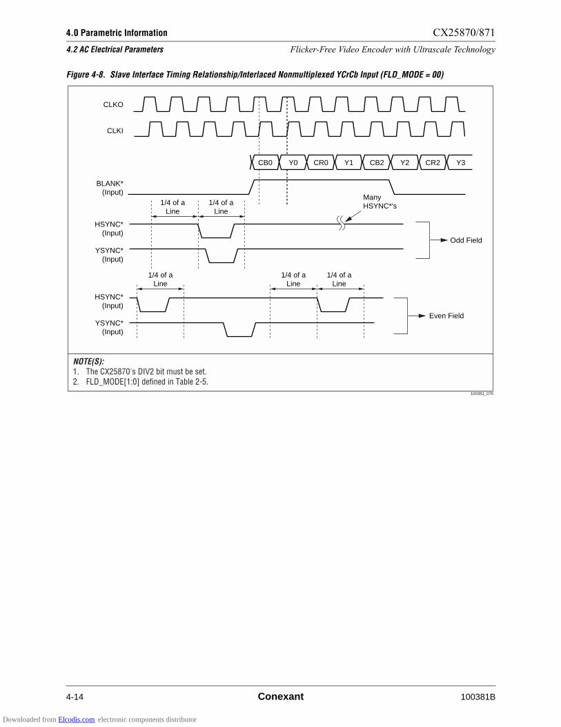
4.0 Parametric Information CX25870/871
4.2 AC Electrical Parameters Flicker-Free Video Encoder with Ultrascale Technology
4-14 Conexant 100381B
Figure 4-8. Slave Interface Timing Relationship/Interlaced Nonmultiplexed YCrCb Input (FLD_MODE = 00)
100381_076
CB0
1/4 of aLine
1/4 of aLine
1/4 of aLine
1/4 of aLine
1/4 of aLine
CLKO
CLKI
Odd Field
ManyHSYNC*'s
Even Field
BLANK*(Input)
HSYNC*(Input)
YSYNC*(Input)
HSYNC*(Input)
YSYNC*(Input)
Y0 CR0 Y1 CB2 Y2 CR2 Y3
NOTE(S):1. The CX25870's DIV2 bit must be set.2. FLD_MODE[1:0] defined in Table 2-5.
Downloaded from Elcodis.com electronic components distributor

CX25870/871 4.0 Parametric Information
Flicker-Free Video Encoder with Ultrascale Technology 4.2 AC Electrical Parameters
100381B Conexant 4-15
Figure 4-9. HDTV Output Horizontal Timing Details: 1080i
100381_089
+300
+300
+300
+700
+350
–300
–300
–300
–350
0
BLANKINGVertical Sync
(Interfaced)
PB,PR(Outputs)
Y,R,G,B(Outputs)
BROAD PULSE
0H
0H
0H<zero>
0
0
z
,
)
*
-
NOTE(S):1. Values for ), *, +, ,, -, and / are given in Table 4-4.2. Sync rise time (/) is not shown here.3. Amplitudes are expressed in mV.
Downloaded from Elcodis.com electronic components distributor
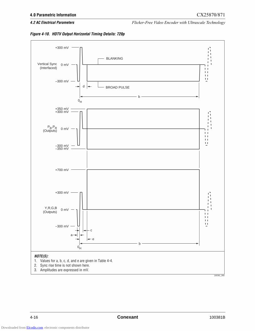
4.0 Parametric Information CX25870/871
4.2 AC Electrical Parameters Flicker-Free Video Encoder with Ultrascale Technology
4-16 Conexant 100381B
Figure 4-10. HDTV Output Horizontal Timing Details: 720p
100381_090
+300 mV
+300 mV
+300 mV
+700 mV
+350 mV
–300 mV
d
b
b
–300 mV
–300 mV
–350 mV
0 mV
BLANKING
Vertical Sync(Interfaced)
PB,PR(Outputs)
Y,R,G,B(Outputs)
BROAD PULSE
0H
0H
0 mV
0 mV
e
ca
NOTE(S):1. Values for a, b, c, d, and e are given in Table 4-4.2. Sync rise time is not shown here.3. Amplitudes are expressed in mV.
Downloaded from Elcodis.com electronic components distributor
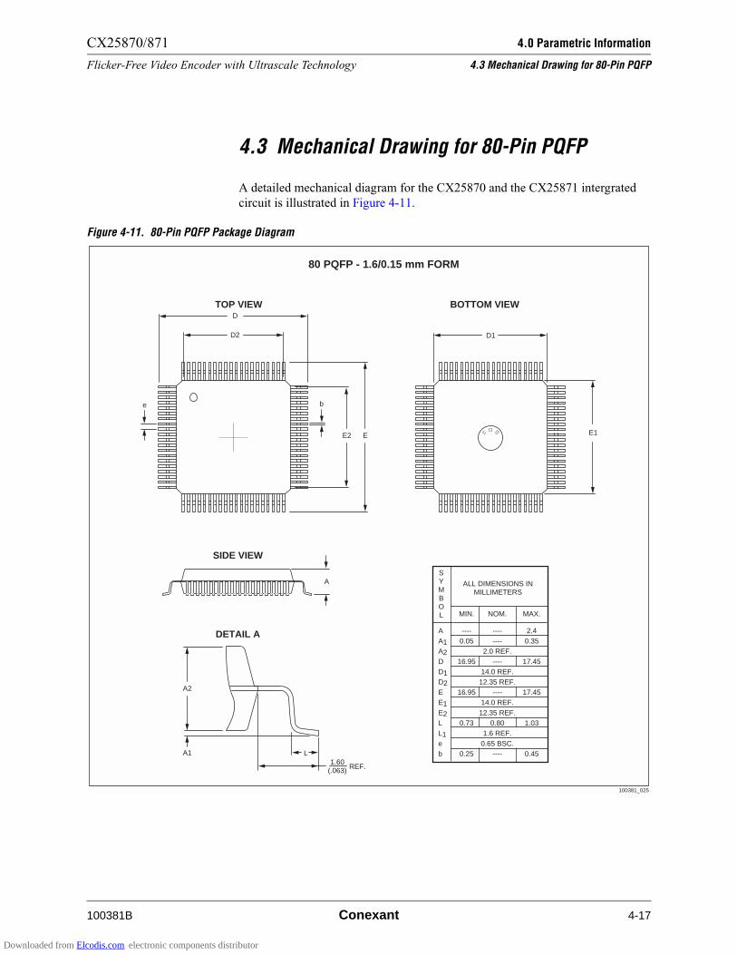
CX25870/871 4.0 Parametric Information
Flicker-Free Video Encoder with Ultrascale Technology 4.3 Mechanical Drawing for 80-Pin PQFP
100381B Conexant 4-17
4.3 Mechanical Drawing for 80-Pin PQFP
A detailed mechanical diagram for the CX25870 and the CX25871 intergrated
circuit is illustrated in Figure 4-11.
Figure 4-11. 80-Pin PQFP Package Diagram
D
E
A
A2
REF.
A11.60
(.063)
L
D1
80 PQFP - 1.6/0.15 mm FORM
E2 E1
e b
D2
SYMBOL
ALL DIMENSIONS INMILLIMETERS
MIN. NOM. MAX.
----0.05
16.95
16.95
0.73
0.25
--------
2.0 REF.----
14.0 REF.12.35 REF.
----14.0 REF.
12.35 REF.0.80
1.6 REF.0.65 BSC.
----
2.40.35
17.45
17.45
1.03
0.45
AA1A2DD1D2EE1E2LL1eb
TOP VIEW BOTTOM VIEW
SIDE VIEW
DETAIL A
100381_025
Downloaded from Elcodis.com electronic components distributor

4.0 Parametric Information CX25870/871
4.3 Mechanical Drawing for 80-Pin PQFP Flicker-Free Video Encoder with Ultrascale Technology
4-18 Conexant 100381B
Downloaded from Elcodis.com electronic components distributor
100381B Conexant A-1
A49
Appendix A Scaling and I/0 Timing Register Calculations
The calculated values are used to program the registers controlling the total active
pixels and lines in the input frame and the output field, as well as the vertical
scaling register and the clock PLL registers. These calculations assume pixel
resolution for synchronizing the graphics controller, master interface operation
unless otherwise stated, and require the following input values:
MFP—Minimum Front Porch Blanking in the Input in Clocks = max
(12, Controller_Minimum_Front_Porch_Blanking_Clocks);
MBP—Minimum Back Porch Blanking in the Input in Clocks = max
(4, Controller_Minimum_Back_Porch_Blanking_Clocks);
VOC—desired Vertical Overscan Compensation (e.g., 0.15)
HOC—desired Horizontal Overscan Compensation (e.g., 0.15)
V_ACTIVEI—Active Lines per Input Frame (e.g., 480 or 600 or 768)
H_ACTIVE—Active Pixels per Input Line (e.g., 640 or 800 or 1024)
ALO—Target Active Lines per Output Field (See Table A-3)
TLO—Total Lines per Output Field (See Table A-3)
ATO—Active Time per Output Line (See Table A-3)
TTO—Total Time per Output Line (See Table A-3)
Tables A-1 and A-2 contain details of the supported video output formats.
Table A-3 details the constant software values depending on the video output.
Figures A-1 through A-8 illustrate allowable overscan compensation pairs for the
most common desktop active resolutions. Tables A-3 through A-27 list the most
common overscan values for the 640 x 480, 800 x 600, and 1024 x 768 active
resolutions that enable dual display on both the VGA monitor and TV.
Downloaded from Elcodis.com electronic components distributor
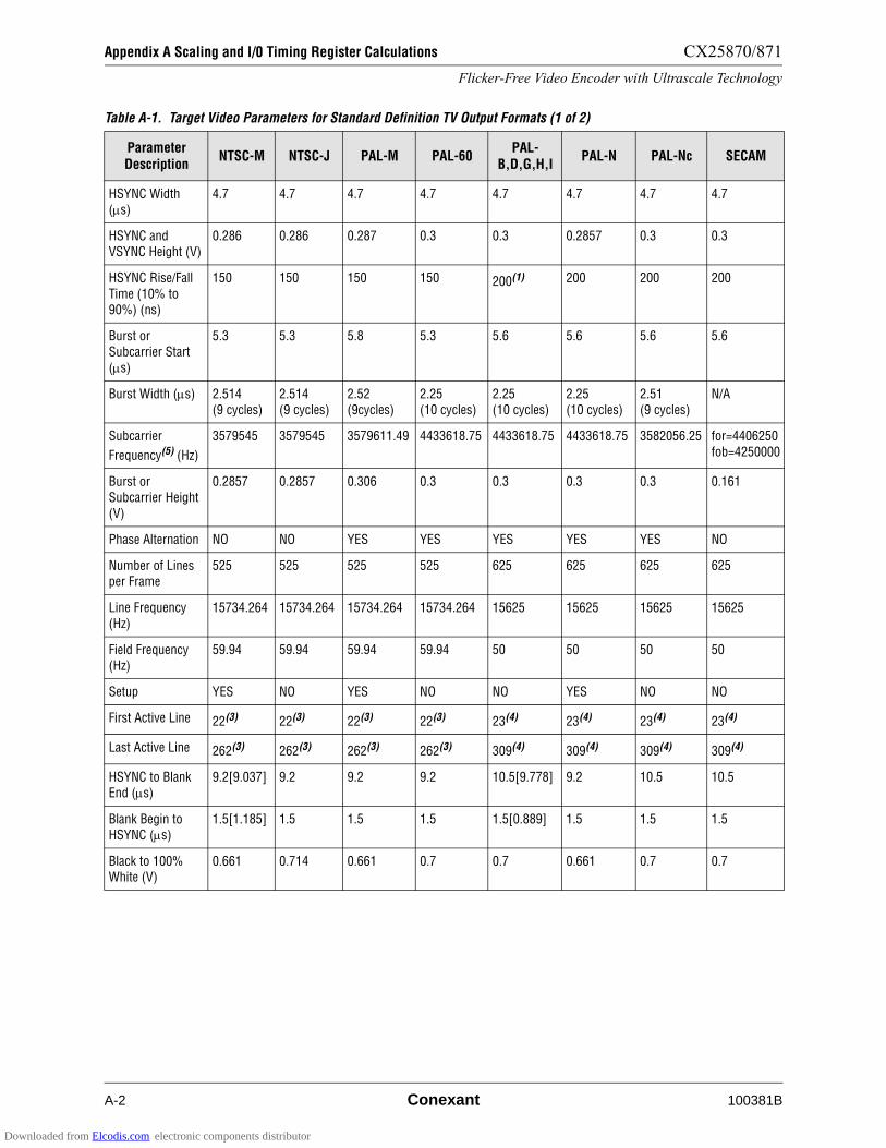
Appendix A Scaling and I/0 Timing Register Calculations CX25870/871
Flicker-Free Video Encoder with Ultrascale Technology
A-2 Conexant 100381B
Table A-1. Target Video Parameters for Standard Definition TV Output Formats (1 of 2)
Parameter Description
NTSC-M NTSC-J PAL-M PAL-60PAL-
B,D,G,H,IPAL-N PAL-Nc SECAM
HSYNC Width (!s)
4.7 4.7 4.7 4.7 4.7 4.7 4.7 4.7
HSYNC and VSYNC Height (V)
0.286 0.286 0.287 0.3 0.3 0.2857 0.3 0.3
HSYNC Rise/Fall
Time (10% to 90%) (ns)
150 150 150 150 200(1) 200 200 200
Burst or Subcarrier Start
(!s)
5.3 5.3 5.8 5.3 5.6 5.6 5.6 5.6
Burst Width (!s) 2.514 (9 cycles)
2.514(9 cycles)
2.52 (9cycles)
2.25 (10 cycles)
2.25 (10 cycles)
2.25 (10 cycles)
2.51 (9 cycles)
N/A
Subcarrier
Frequency(5) (Hz)
3579545 3579545 3579611.49 4433618.75 4433618.75 4433618.75 3582056.25 for=4406250fob=4250000
Burst or
Subcarrier Height (V)
0.2857 0.2857 0.306 0.3 0.3 0.3 0.3 0.161
Phase Alternation NO NO YES YES YES YES YES NO
Number of Lines per Frame
525 525 525 525 625 625 625 625
Line Frequency
(Hz)
15734.264 15734.264 15734.264 15734.264 15625 15625 15625 15625
Field Frequency (Hz)
59.94 59.94 59.94 59.94 50 50 50 50
Setup YES NO YES NO NO YES NO NO
First Active Line 22(3) 22(3) 22(3) 22(3) 23(4) 23(4) 23(4) 23(4)
Last Active Line 262(3) 262(3) 262(3) 262(3) 309(4) 309(4) 309(4) 309(4)
HSYNC to Blank End (!s)
9.2[9.037] 9.2 9.2 9.2 10.5[9.778] 9.2 10.5 10.5
Blank Begin to HSYNC (!s)
1.5[1.185] 1.5 1.5 1.5 1.5[0.889] 1.5 1.5 1.5
Black to 100% White (V)
0.661 0.714 0.661 0.7 0.7 0.661 0.7 0.7
Downloaded from Elcodis.com electronic components distributor

CX25870/871 Appendix A Scaling and I/0 Timing Register Calculations
Flicker-Free Video Encoder with Ultrascale Technology
100381B Conexant A-3
Number of Lines
each for Vertical Serration, Equalization
3 3 3 3 2.5 3 2.5 2.5
NOTE(S):(1) Value for PAL-I is 250 ns.2. ITU-R BT.601 blanking values given in square brackets [].(3) Using NTSC line numbering convention from ITU-R BT.470.(4) Using PAL line numbering convention from ITU-R BT.470.(5) When programming the subcarrier increment, use relationship of Fsc to Fh as given in ITU-R BT.470 instead of Fsc to Fclk.
Table A-1. Target Video Parameters for Standard Definition TV Output Formats (2 of 2)
Parameter Description
NTSC-M NTSC-J PAL-M PAL-60PAL-
B,D,G,H,IPAL-N PAL-Nc SECAM
Table A-2. Key Parameters for Supported Standard Definition Video Output Formats
Mode NTSCNTSC-60Hz
PAL-BDGHI
PAL-N PAL-Nc PAL-M PAL-60
FSC (Hz) 3,579,545 3,579,545 4,433,618.75 4,433,618.75 3,582,056.25 3,575,611.88 4,433,619.49
Burst Start 5.3 !s 5.3 !s 5.60 !s 5.60 !s 5.60 !s 5.80 !s 5.60 !s
Burst End 7.82 !s 7.82 !s 7.85 !s 7.85 !s 8.11 !s 8.32 !s 7.85 !s
HSYNC
Width(1)
4.70 !s 4.70 !s 4.70 !s 4.70 !s 4.70 !s 4.70 !s 4.70 !s
HSYNC
Frequency(1)
63.555 !s 64 !s 64 !s 64 !s 64 !s 63.555 !s 64 !s
Active Begin 9.40 !s 9.40 !s 10.5 !s 9.40 !s 10.5 !s 9.40 !s 10.5 !s
Image Center 35.667 !s 35.667 !s 36.407 !s 35.667 !s 36.407 !s 35.667 !s 36.407 !s
Blank Begin to
HSYNC(1)
1.50 !s 1.50 !s 1.50 !s 1.50 !s 1.50 !s 1.50 !s 1.50 !s
NOTE(S):(1) HSYNC in this table refers to the analog horizontal synchronization pulse that starts every scan line.
Table A-3. Constant Values Dependent on Encoding Mode
ModesInterlaced NonInterlaced
PAL NTSC PAL NTSC
ALO 288 243 288 243
TLO 312.5 262.5 312 262
ATO 52.0 !s 52.65556 !s 52.0 !s 52.65556 !s
TTO 64.0 !s 63.55556 !s 64.0 !s 63.55556 !s
Downloaded from Elcodis.com electronic components distributor

Appendix A Scaling and I/0 Timing Register Calculations CX25870/871
Flicker-Free Video Encoder with Ultrascale Technology
A-4 Conexant 100381B
Figure A-1. Allowable Overscan Compensation Ratios for Dual Display, 640x480 Input, NTSC Output with 20 Clock HBlank Period
8 10 12 14 16 18 20 228
10
12
14
16
18
20
22
Vertical Overscan Compensation Percentage
Hor
izon
tal O
vers
can
Com
pens
atio
n P
erce
ntag
e
Overscan Compensation Pecentage Pairs for 640x480 NTSC
100381_026
= Pixel Clock Solution
= 8-Cycle Character Clock Solution
= 9-Cycle Character Clock Solution
Legend:
NOTE(S):Use this chart for PAL-M and PAL-60 allowable overscan ratios.
Downloaded from Elcodis.com electronic components distributor
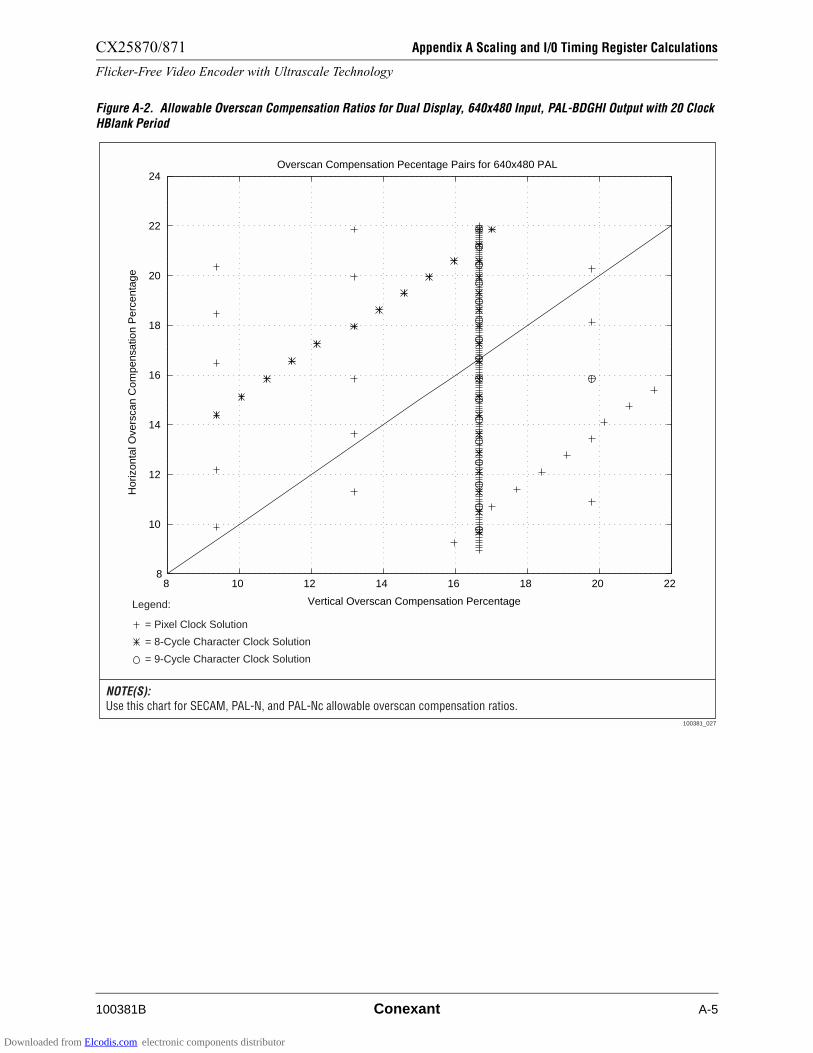
CX25870/871 Appendix A Scaling and I/0 Timing Register Calculations
Flicker-Free Video Encoder with Ultrascale Technology
100381B Conexant A-5
Figure A-2. Allowable Overscan Compensation Ratios for Dual Display, 640x480 Input, PAL-BDGHI Output with 20 Clock HBlank Period
8 10 12 14 16 18 20 228
10
12
14
16
18
20
22
24
Vertical Overscan Compensation Percentage
Hor
izon
tal O
vers
can
Com
pens
atio
n P
erce
ntag
e
Overscan Compensation Pecentage Pairs for 640x480 PAL
100381_027
= Pixel Clock Solution
= 8-Cycle Character Clock Solution
= 9-Cycle Character Clock Solution
Legend:
NOTE(S):Use this chart for SECAM, PAL-N, and PAL-Nc allowable overscan compensation ratios.
Downloaded from Elcodis.com electronic components distributor

Appendix A Scaling and I/0 Timing Register Calculations CX25870/871
Flicker-Free Video Encoder with Ultrascale Technology
A-6 Conexant 100381B
Figure A-3. Allowable Overscan Compensation Ratios for Dual Display, 800x600 Input, NTSC Output
NOTE(S):Use this chart for PAL-M and PAL-60 allowable overscan ratios.
8 10 12 14 16 18 20 228
10
12
14
16
18
20
22
24
Vertical Overscan Compensation Percentage
Hor
izon
tal O
vers
can
Com
pens
atio
n P
erce
ntag
eOverscan Compensation Percentage Pairs for 800x600 NTSC
0 µs Horizontal Blanking
1 µs
2 µs
3 µs
.75 µs
100381_028
= Pixel Clock Solution
= 8-Cycle Character Clock Solution
= 9-Cycle Character Clock Solution
Legend:
Downloaded from Elcodis.com electronic components distributor

CX25870/871 Appendix A Scaling and I/0 Timing Register Calculations
Flicker-Free Video Encoder with Ultrascale Technology
100381B Conexant A-7
Figure A-4. Allowable Overscan Compensation Ratios for Dual Display, 800x600 Input, PAL–BDGHI Output, Standard Clocking Mode
Downloaded from Elcodis.com electronic components distributor

Appendix A Scaling and I/0 Timing Register Calculations CX25870/871
Flicker-Free Video Encoder with Ultrascale Technology
A-8 Conexant 100381B
Figure A-5. Allowable Overscan Compensation Ratios for Dual Display, 800x600 Input, NTSC Output in 3:2 Clocking Mode
8 10 12 14 16 18 20 228
10
12
14
16
18
20
22
Vertical Overscan Compensation Percentage
Hor
izon
tal O
vers
can
Com
pens
atio
n P
erce
ntag
e
LEGEND
= Pixel Clock Solution
= 8-Cycle Character Clock Solution
= 9-Cycle Character Clock Solution
NOTE(S):1. All overscan solutions on this chart can be enabled by a data master that requires no more than 4 µs of MBlank time per line.2. Use this chart for PAL-M and PAL-60 allowable overscan ratios.
Downloaded from Elcodis.com electronic components distributor

CX25870/871 Appendix A Scaling and I/0 Timing Register Calculations
Flicker-Free Video Encoder with Ultrascale Technology
100381B Conexant A-9
Figure A-6. Allowable Overscan Compensation Ratios for Dual Display, 800x600 Input, PAL-BDGHI Output in 3:2 Clocking Mode
8 10 12 14 16 18 20 228
10
12
14
16
18
20
22
Vertical Overscan Compensation Percentage
Hor
izon
tal O
vers
can
Com
pens
atio
n P
erce
ntag
e
LEGEND
= Pixel Clock Solution
= 8-Cycle Character Clock Solution
= 9-Cycle Character Clock Solution
100381_066
NOTE(S):1. All overscan solutions on this chart can be enabled by a data master that requires no more than 8 µs of HBlank time per line.2. Use this chart for SECAM, PAL-N, and PAL-Nc allowable overscan compensation ratios.
Downloaded from Elcodis.com electronic components distributor
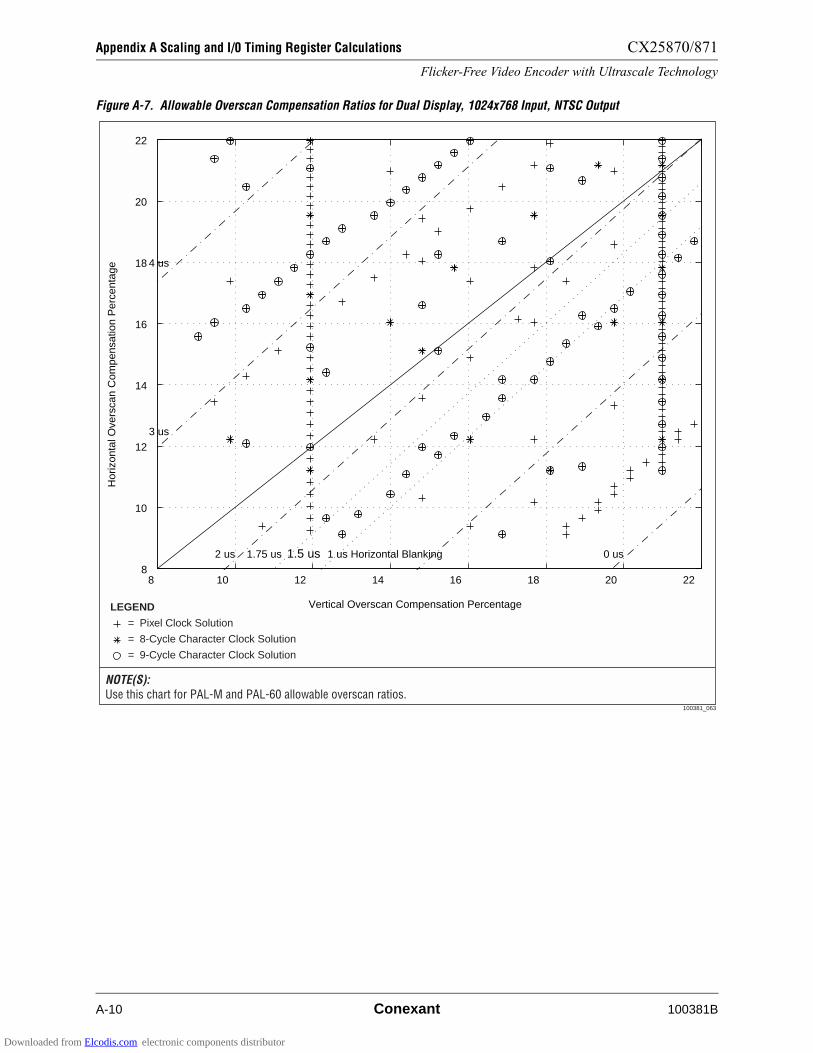
Appendix A Scaling and I/0 Timing Register Calculations CX25870/871
Flicker-Free Video Encoder with Ultrascale Technology
A-10 Conexant 100381B
Figure A-7. Allowable Overscan Compensation Ratios for Dual Display, 1024x768 Input, NTSC Output
NOTE(S):Use this chart for PAL-M and PAL-60 allowable overscan ratios.
8 10 12 14 16 18 20 228
10
12
14
16
18
20
22
0 us1 us Horizontal Blanking1.5 us1.75 us2 us
3 us
4 us
Hor
izon
tal O
vers
can
Com
pens
atio
n P
erce
ntag
e
Vertical Overscan Compensation Percentage
100381_063
LEGEND
= Pixel Clock Solution
= 8-Cycle Character Clock Solution
= 9-Cycle Character Clock Solution
Downloaded from Elcodis.com electronic components distributor
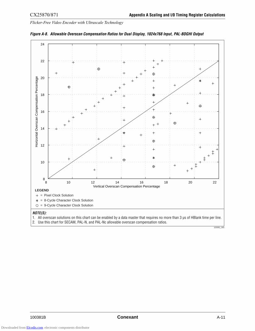
CX25870/871 Appendix A Scaling and I/0 Timing Register Calculations
Flicker-Free Video Encoder with Ultrascale Technology
100381B Conexant A-11
Figure A-8. Allowable Overscan Compensation Ratios for Dual Display, 1024x768 Input, PAL-BDGHI Output
8 10 12 14 16 18 20 228
10
12
14
16
18
20
22
24
Vertical Overscan Compensation Percentage
Hor
izon
tal O
vers
can
Com
pens
atio
n P
erce
ntag
e
LEGEND
= Pixel Clock Solution
= 8-Cycle Character Clock Solution
= 9-Cycle Character Clock Solution
100381_065
NOTE(S):1. All overscan solutions on this chart can be enabled by a data master that requires no more than 3 µs of HBlank time per line.2. Use this chart for SECAM, PAL-N, and PAL-Nc allowable overscan compensation ratios.
Downloaded from Elcodis.com electronic components distributor
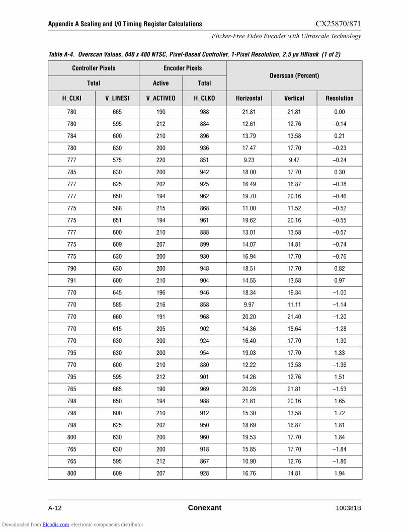
Appendix A Scaling and I/0 Timing Register Calculations CX25870/871
Flicker-Free Video Encoder with Ultrascale Technology
A-12 Conexant 100381B
Table A-4. Overscan Values, 640 x 480 NTSC, Pixel-Based Controller, 1-Pixel Resolution, 2.5 µs HBlank (1 of 2)
Controller Pixels Encoder PixelsOverscan (Percent)
Total Active Total
H_CLKI V_LINESI V_ACTIVEO H_CLKO Horizontal Vertical Resolution
780 665 190 988 21.81 21.81 0.00
780 595 212 884 12.61 12.76 –0.14
784 600 210 896 13.79 13.58 0.21
780 630 200 936 17.47 17.70 –0.23
777 575 220 851 9.23 9.47 –0.24
785 630 200 942 18.00 17.70 0.30
777 625 202 925 16.49 16.87 –0.38
777 650 194 962 19.70 20.16 –0.46
775 588 215 868 11.00 11.52 –0.52
775 651 194 961 19.62 20.16 –0.55
777 600 210 888 13.01 13.58 –0.57
775 609 207 899 14.07 14.81 –0.74
775 630 200 930 16.94 17.70 –0.76
790 630 200 948 18.51 17.70 0.82
791 600 210 904 14.55 13.58 0.97
770 645 196 946 18.34 19.34 –1.00
770 585 216 858 9.97 11.11 –1.14
770 660 191 968 20.20 21.40 –1.20
770 615 205 902 14.36 15.64 –1.28
770 630 200 924 16.40 17.70 –1.30
795 630 200 954 19.03 17.70 1.33
770 600 210 880 12.22 13.58 –1.36
795 595 212 901 14.26 12.76 1.51
765 665 190 969 20.28 21.81 –1.53
798 650 194 988 21.81 20.16 1.65
798 600 210 912 15.30 13.58 1.72
798 625 202 950 18.69 16.87 1.81
800 630 200 960 19.53 17.70 1.84
765 630 200 918 15.85 17.70 –1.84
765 595 212 867 10.90 12.76 –1.86
800 609 207 928 16.76 14.81 1.94
Downloaded from Elcodis.com electronic components distributor

CX25870/871 Appendix A Scaling and I/0 Timing Register Calculations
Flicker-Free Video Encoder with Ultrascale Technology
100381B Conexant A-13
798 575 220 874 11.62 9.47 2.15
763 600 210 872 11.41 13.58 –2.17
800 588 215 896 13.79 11.52 2.26
805 630 200 966 20.03 17.70 2.34
760 630 200 912 15.30 17.70 –2.40
805 615 205 943 18.08 15.64 2.44
805 600 210 920 16.03 13.58 2.45
805 645 196 989 21.89 19.34 2.55
756 650 194 936 17.47 20.16 –2.69
756 625 202 900 14.17 16.87 –2.70
805 585 216 897 13.88 11.11 2.77
810 630 200 972 20.53 17.70 2.83
755 630 200 906 14.74 17.70 –2.96
805 570 222 874 11.62 8.64 2.97
756 600 210 864 10.59 13.58 –2.99
Table A-4. Overscan Values, 640 x 480 NTSC, Pixel-Based Controller, 1-Pixel Resolution, 2.5 µs HBlank (2 of 2)
Controller Pixels Encoder PixelsOverscan (Percent)
Total Active Total
H_CLKI V_LINESI V_ACTIVEO H_CLKO Horizontal Vertical Resolution
Downloaded from Elcodis.com electronic components distributor

Appendix A Scaling and I/0 Timing Register Calculations CX25870/871
Flicker-Free Video Encoder with Ultrascale Technology
A-14 Conexant 100381B
Table A-5. Overscan Values, 640 x 480 NTSC, Character Clock-Based Controller, 8-Pixel Resolution, 2.5 µs HBlank
Controller Pixels Encoder PixelsOverscan (Percent)
Total Active Total
H_CLKI V_LINESI V_ACTIVEO H_CLKO Horizontal Vertical Resolution
784 600 210 896 13.79 13.58 0.21
800 630 200 960 19.53 17.70 1.84
800 609 207 928 16.76 14.81 1.94
800 588 215 896 13.79 11.52 2.26
760 630 200 912 15.30 17.70 –2.40
840 615 205 984 21.50 15.64 5.86
840 600 210 960 19.53 13.58 5.95
840 610 207 976 20.85 14.81 6.04
840 595 212 952 18.86 12.76 6.10
840 605 209 968 20.20 13.99 6.21
840 590 214 944 18.17 11.93 6.23
840 585 216 936 17.47 11.11 6.36
840 580 218 928 16.76 10.29 6.47
720 665 190 912 15.30 21.81 –6.51
840 575 220 920 16.03 9.47 6.57
840 570 222 912 15.30 8.64 6.66
720 630 200 864 10.59 17.70 –7.10
Downloaded from Elcodis.com electronic components distributor
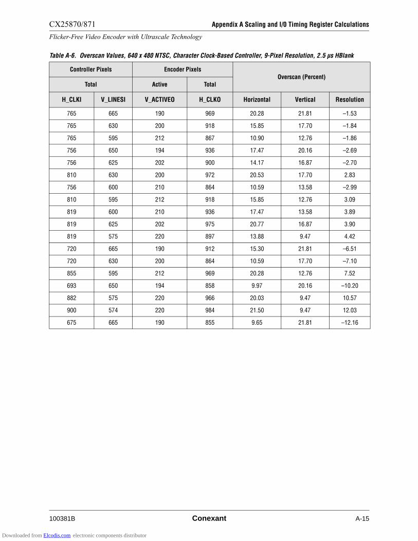
CX25870/871 Appendix A Scaling and I/0 Timing Register Calculations
Flicker-Free Video Encoder with Ultrascale Technology
100381B Conexant A-15
Table A-6. Overscan Values, 640 x 480 NTSC, Character Clock-Based Controller, 9-Pixel Resolution, 2.5 µs HBlank
Controller Pixels Encoder PixelsOverscan (Percent)
Total Active Total
H_CLKI V_LINESI V_ACTIVEO H_CLKO Horizontal Vertical Resolution
765 665 190 969 20.28 21.81 –1.53
765 630 200 918 15.85 17.70 –1.84
765 595 212 867 10.90 12.76 –1.86
756 650 194 936 17.47 20.16 –2.69
756 625 202 900 14.17 16.87 –2.70
810 630 200 972 20.53 17.70 2.83
756 600 210 864 10.59 13.58 –2.99
810 595 212 918 15.85 12.76 3.09
819 600 210 936 17.47 13.58 3.89
819 625 202 975 20.77 16.87 3.90
819 575 220 897 13.88 9.47 4.42
720 665 190 912 15.30 21.81 –6.51
720 630 200 864 10.59 17.70 –7.10
855 595 212 969 20.28 12.76 7.52
693 650 194 858 9.97 20.16 –10.20
882 575 220 966 20.03 9.47 10.57
900 574 220 984 21.50 9.47 12.03
675 665 190 855 9.65 21.81 –12.16
Downloaded from Elcodis.com electronic components distributor

Appendix A Scaling and I/0 Timing Register Calculations CX25870/871
Flicker-Free Video Encoder with Ultrascale Technology
A-16 Conexant 100381B
Table A-7. Overscan Values, 640 x 480 PAL-BDGHI, Pixel-Based Controller, 1-Pixel Resolution, 2.5 µs HBlank (1 of 3)
Controller Pixels Encoder PixelsOverscan (Percent)
Total Active Total
H_CLKI V_LINESI V_ACTIVEO H_CLKO Horizontal Vertical Resolution
945 625 240 945 16.65 16.67 –0.02
946 625 240 946 16.73 16.67 0.07
944 625 240 944 16.56 16.67 –0.11
947 625 240 947 16.82 16.67 0.16
943 625 240 943 16.47 16.67 –0.20
948 625 240 948 16.91 16.67 0.24
942 625 240 942 16.38 16.67 –0.29
949 625 240 949 17.00 16.67 0.33
941 625 240 941 16.29 16.67 –0.37
950 625 240 950 17.09 16.67 0.42
950 600 250 912 13.63 13.19 0.44
940 625 240 940 16.20 16.67 –0.46
950 650 231 988 20.27 19.79 0.48
950 575 261 874 9.88 9.38 0.50
951 625 240 951 17.17 16.67 0.51
939 625 240 939 16.11 16.67 –0.55
952 625 240 952 17.26 16.67 0.59
938 625 240 938 16.02 16.67 –0.64
953 625 240 953 17.35 16.67 0.68
937 625 240 937 15.93 16.67 –0.73
954 625 240 954 17.43 16.67 0.77
936 625 240 936 15.84 16.67 –0.82
955 625 240 955 17.52 16.67 0.85
935 625 240 935 15.75 16.67 –0.91
956 625 240 956 17.61 16.67 0.94
934 625 240 934 15.66 16.67 –1.00
957 625 240 957 17.69 16.67 1.02
933 625 240 933 15.57 16.67 –1.09
958 625 240 958 17.78 16.67 1.11
932 625 240 932 15.48 16.67 –1.18
959 625 240 959 17.86 16.67 1.20
Downloaded from Elcodis.com electronic components distributor
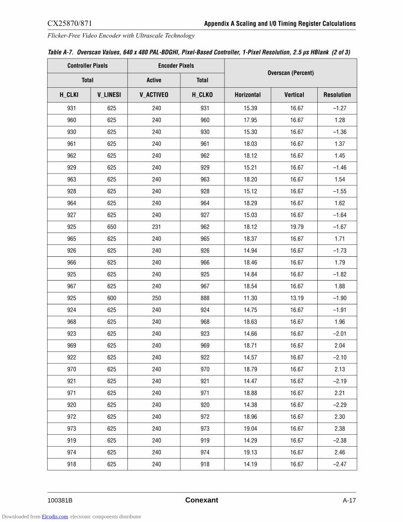
CX25870/871 Appendix A Scaling and I/0 Timing Register Calculations
Flicker-Free Video Encoder with Ultrascale Technology
100381B Conexant A-17
931 625 240 931 15.39 16.67 –1.27
960 625 240 960 17.95 16.67 1.28
930 625 240 930 15.30 16.67 –1.36
961 625 240 961 18.03 16.67 1.37
962 625 240 962 18.12 16.67 1.45
929 625 240 929 15.21 16.67 –1.46
963 625 240 963 18.20 16.67 1.54
928 625 240 928 15.12 16.67 –1.55
964 625 240 964 18.29 16.67 1.62
927 625 240 927 15.03 16.67 –1.64
925 650 231 962 18.12 19.79 –1.67
965 625 240 965 18.37 16.67 1.71
926 625 240 926 14.94 16.67 –1.73
966 625 240 966 18.46 16.67 1.79
925 625 240 925 14.84 16.67 –1.82
967 625 240 967 18.54 16.67 1.88
925 600 250 888 11.30 13.19 –1.90
924 625 240 924 14.75 16.67 –1.91
968 625 240 968 18.63 16.67 1.96
923 625 240 923 14.66 16.67 –2.01
969 625 240 969 18.71 16.67 2.04
922 625 240 922 14.57 16.67 –2.10
970 625 240 970 18.79 16.67 2.13
921 625 240 921 14.47 16.67 –2.19
971 625 240 971 18.88 16.67 2.21
920 625 240 920 14.38 16.67 –2.29
972 625 240 972 18.96 16.67 2.30
973 625 240 973 19.04 16.67 2.38
919 625 240 919 14.29 16.67 –2.38
974 625 240 974 19.13 16.67 2.46
918 625 240 918 14.19 16.67 –2.47
Table A-7. Overscan Values, 640 x 480 PAL-BDGHI, Pixel-Based Controller, 1-Pixel Resolution, 2.5 µs HBlank (2 of 3)
Controller Pixels Encoder PixelsOverscan (Percent)
Total Active Total
H_CLKI V_LINESI V_ACTIVEO H_CLKO Horizontal Vertical Resolution
Downloaded from Elcodis.com electronic components distributor
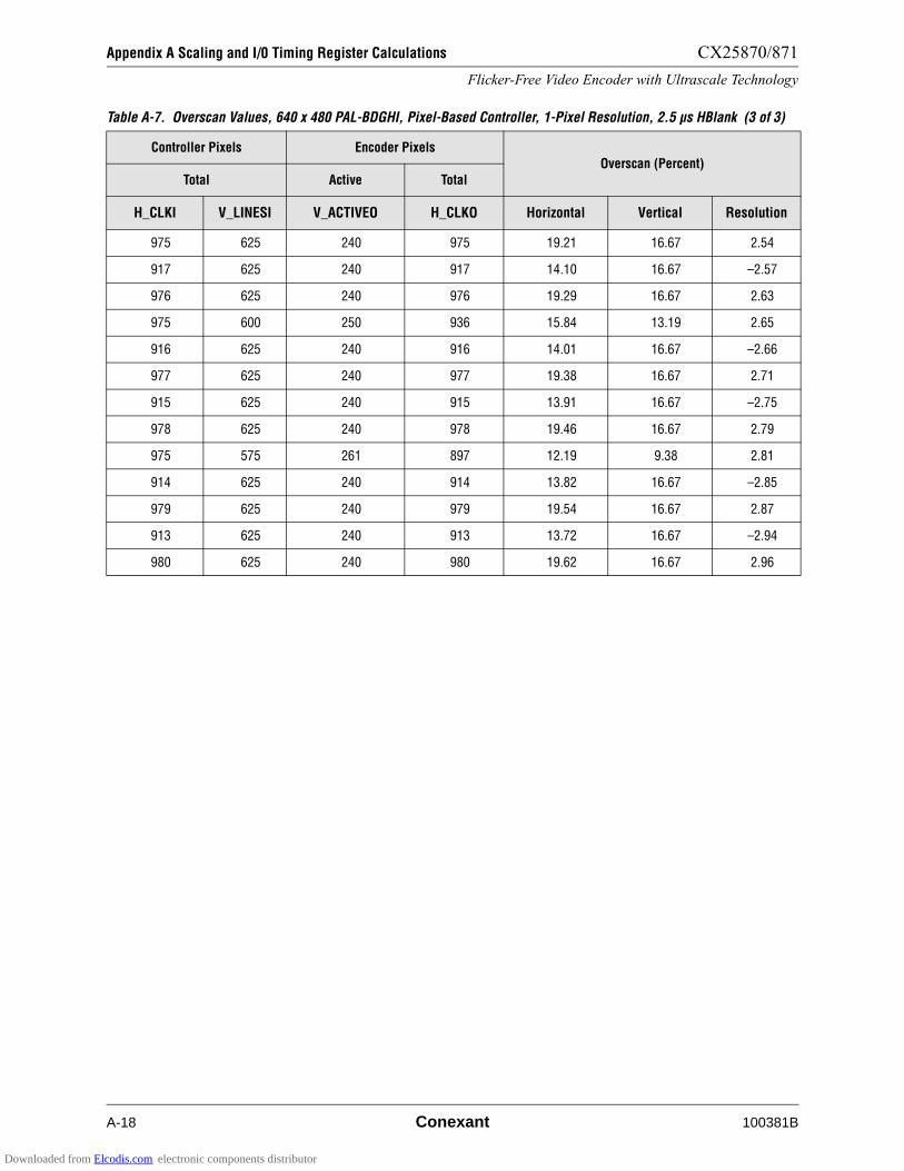
Appendix A Scaling and I/0 Timing Register Calculations CX25870/871
Flicker-Free Video Encoder with Ultrascale Technology
A-18 Conexant 100381B
975 625 240 975 19.21 16.67 2.54
917 625 240 917 14.10 16.67 –2.57
976 625 240 976 19.29 16.67 2.63
975 600 250 936 15.84 13.19 2.65
916 625 240 916 14.01 16.67 –2.66
977 625 240 977 19.38 16.67 2.71
915 625 240 915 13.91 16.67 –2.75
978 625 240 978 19.46 16.67 2.79
975 575 261 897 12.19 9.38 2.81
914 625 240 914 13.82 16.67 –2.85
979 625 240 979 19.54 16.67 2.87
913 625 240 913 13.72 16.67 –2.94
980 625 240 980 19.62 16.67 2.96
Table A-7. Overscan Values, 640 x 480 PAL-BDGHI, Pixel-Based Controller, 1-Pixel Resolution, 2.5 µs HBlank (3 of 3)
Controller Pixels Encoder PixelsOverscan (Percent)
Total Active Total
H_CLKI V_LINESI V_ACTIVEO H_CLKO Horizontal Vertical Resolution
Downloaded from Elcodis.com electronic components distributor
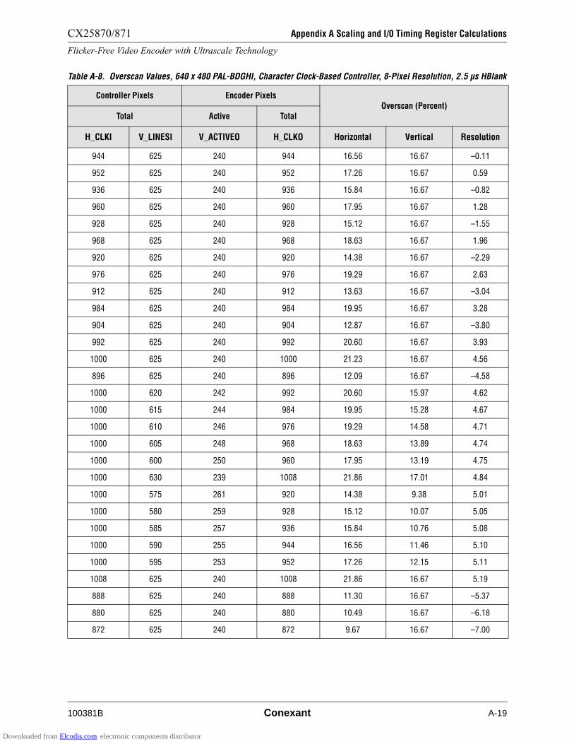
CX25870/871 Appendix A Scaling and I/0 Timing Register Calculations
Flicker-Free Video Encoder with Ultrascale Technology
100381B Conexant A-19
Table A-8. Overscan Values, 640 x 480 PAL-BDGHI, Character Clock-Based Controller, 8-Pixel Resolution, 2.5 µs HBlank
Controller Pixels Encoder PixelsOverscan (Percent)
Total Active Total
H_CLKI V_LINESI V_ACTIVEO H_CLKO Horizontal Vertical Resolution
944 625 240 944 16.56 16.67 –0.11
952 625 240 952 17.26 16.67 0.59
936 625 240 936 15.84 16.67 –0.82
960 625 240 960 17.95 16.67 1.28
928 625 240 928 15.12 16.67 –1.55
968 625 240 968 18.63 16.67 1.96
920 625 240 920 14.38 16.67 –2.29
976 625 240 976 19.29 16.67 2.63
912 625 240 912 13.63 16.67 –3.04
984 625 240 984 19.95 16.67 3.28
904 625 240 904 12.87 16.67 –3.80
992 625 240 992 20.60 16.67 3.93
1000 625 240 1000 21.23 16.67 4.56
896 625 240 896 12.09 16.67 –4.58
1000 620 242 992 20.60 15.97 4.62
1000 615 244 984 19.95 15.28 4.67
1000 610 246 976 19.29 14.58 4.71
1000 605 248 968 18.63 13.89 4.74
1000 600 250 960 17.95 13.19 4.75
1000 630 239 1008 21.86 17.01 4.84
1000 575 261 920 14.38 9.38 5.01
1000 580 259 928 15.12 10.07 5.05
1000 585 257 936 15.84 10.76 5.08
1000 590 255 944 16.56 11.46 5.10
1000 595 253 952 17.26 12.15 5.11
1008 625 240 1008 21.86 16.67 5.19
888 625 240 888 11.30 16.67 –5.37
880 625 240 880 10.49 16.67 –6.18
872 625 240 872 9.67 16.67 –7.00
Downloaded from Elcodis.com electronic components distributor
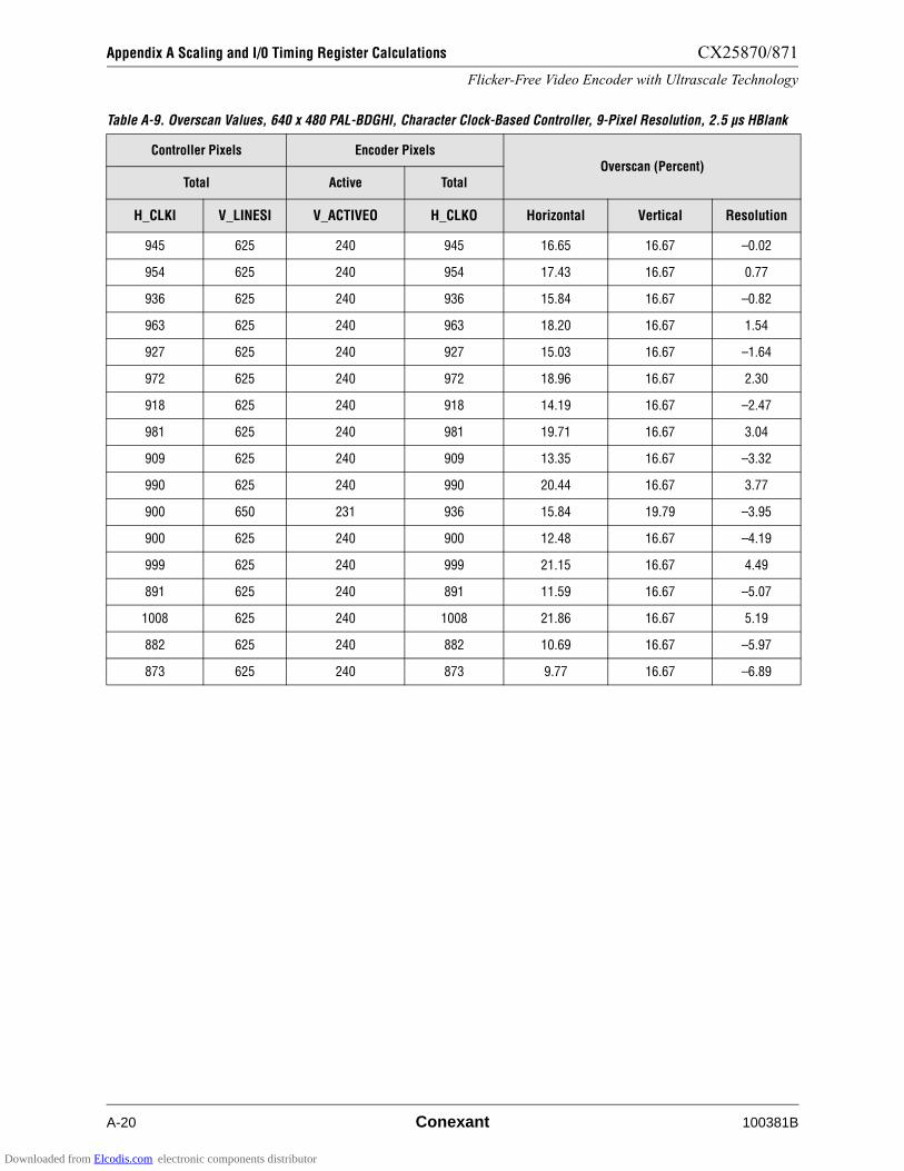
Appendix A Scaling and I/0 Timing Register Calculations CX25870/871
Flicker-Free Video Encoder with Ultrascale Technology
A-20 Conexant 100381B
Table A-9. Overscan Values, 640 x 480 PAL-BDGHI, Character Clock-Based Controller, 9-Pixel Resolution, 2.5 µs HBlank
Controller Pixels Encoder PixelsOverscan (Percent)
Total Active Total
H_CLKI V_LINESI V_ACTIVEO H_CLKO Horizontal Vertical Resolution
945 625 240 945 16.65 16.67 –0.02
954 625 240 954 17.43 16.67 0.77
936 625 240 936 15.84 16.67 –0.82
963 625 240 963 18.20 16.67 1.54
927 625 240 927 15.03 16.67 –1.64
972 625 240 972 18.96 16.67 2.30
918 625 240 918 14.19 16.67 –2.47
981 625 240 981 19.71 16.67 3.04
909 625 240 909 13.35 16.67 –3.32
990 625 240 990 20.44 16.67 3.77
900 650 231 936 15.84 19.79 –3.95
900 625 240 900 12.48 16.67 –4.19
999 625 240 999 21.15 16.67 4.49
891 625 240 891 11.59 16.67 –5.07
1008 625 240 1008 21.86 16.67 5.19
882 625 240 882 10.69 16.67 –5.97
873 625 240 873 9.77 16.67 –6.89
Downloaded from Elcodis.com electronic components distributor

CX25870/871 Appendix A Scaling and I/0 Timing Register Calculations
Flicker-Free Video Encoder with Ultrascale Technology
100381B Conexant A-21
Table A-10. Overscan Values, 800 x 600 NTSC, Pixel-Based Controller, 1-Pixel Resolution (1 of 4)
Controller Pixels Encoder PixelsOverscan (Percent)
Total Active Total
H_CLKI V_LINESI V_ACTIVEO H_CLKO Horizontal Vertical Resolution
800 777 203 1184 18.45 16.46 1.98
800 819 193 1248 22.63 20.58 2.05
800 798 198 1216 20.59 18.52 2.07
800 756 209 1152 16.18 13.99 2.19
800 714 221 1088 11.25 9.05 2.20
800 735 215 1120 13.79 11.52 2.26
805 825 191 1265 23.67 21.40 2.27
805 780 202 1196 19.26 16.87 2.39
805 750 210 1150 16.03 13.58 2.45
805 765 206 1173 17.68 15.23 2.45
805 810 195 1242 22.25 19.75 2.50
805 720 219 1104 12.54 9.88 2.66
805 795 199 1219 20.79 18.11 2.68
805 735 215 1127 14.32 11.52 2.80
810 805 196 1242 22.25 19.34 2.91
810 770 205 1188 18.72 15.64 3.08
812 750 210 1160 16.76 13.58 3.18
810 735 215 1134 14.85 11.52 3.33
819 800 197 1248 22.63 18.93 3.70
815 735 215 1141 15.37 11.52 3.85
819 750 210 1170 17.47 13.58 3.89
819 775 204 1209 20.13 16.05 4.08
825 805 196 1265 23.67 19.34 4.33
819 725 218 1131 14.62 10.29 4.34
825 784 201 1232 21.62 17.28 4.34
820 735 215 1148 15.89 11.52 4.37
825 777 203 1221 20.92 16.46 4.46
825 798 198 1254 23.00 18.52 4.48
825 770 205 1210 20.20 15.64 4.56
826 750 210 1180 18.17 13.58 4.59
825 791 200 1243 22.32 17.70 4.62
Downloaded from Elcodis.com electronic components distributor
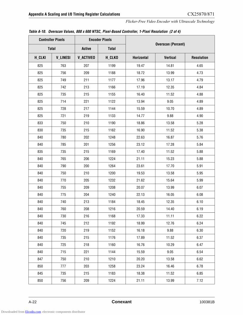
Appendix A Scaling and I/0 Timing Register Calculations CX25870/871
Flicker-Free Video Encoder with Ultrascale Technology
A-22 Conexant 100381B
825 763 207 1199 19.47 14.81 4.65
825 756 209 1188 18.72 13.99 4.73
825 749 211 1177 17.96 13.17 4.79
825 742 213 1166 17.19 12.35 4.84
825 735 215 1155 16.40 11.52 4.88
825 714 221 1122 13.94 9.05 4.89
825 728 217 1144 15.59 10.70 4.89
825 721 219 1133 14.77 9.88 4.90
833 750 210 1190 18.86 13.58 5.28
830 735 215 1162 16.90 11.52 5.38
840 780 202 1248 22.63 16.87 5.76
840 785 201 1256 23.12 17.28 5.84
835 735 215 1169 17.40 11.52 5.88
840 765 206 1224 21.11 15.23 5.88
840 790 200 1264 23.61 17.70 5.91
840 750 210 1200 19.53 13.58 5.95
840 770 205 1232 21.62 15.64 5.99
840 755 209 1208 20.07 13.99 6.07
840 775 204 1240 22.13 16.05 6.08
840 740 213 1184 18.45 12.35 6.10
840 760 208 1216 20.59 14.40 6.19
840 730 216 1168 17.33 11.11 6.22
840 745 212 1192 18.99 12.76 6.24
840 720 219 1152 16.18 9.88 6.30
840 735 215 1176 17.89 11.52 6.37
840 725 218 1160 16.76 10.29 6.47
840 715 221 1144 15.59 9.05 6.54
847 750 210 1210 20.20 13.58 6.62
850 777 203 1258 23.24 16.46 6.78
845 735 215 1183 18.38 11.52 6.85
850 756 209 1224 21.11 13.99 7.12
Table A-10. Overscan Values, 800 x 600 NTSC, Pixel-Based Controller, 1-Pixel Resolution (2 of 4)
Controller Pixels Encoder PixelsOverscan (Percent)
Total Active Total
H_CLKI V_LINESI V_ACTIVEO H_CLKO Horizontal Vertical Resolution
Downloaded from Elcodis.com electronic components distributor

CX25870/871 Appendix A Scaling and I/0 Timing Register Calculations
Flicker-Free Video Encoder with Ultrascale Technology
100381B Conexant A-23
854 750 210 1220 20.85 13.58 7.27
850 735 215 1190 18.86 11.52 7.33
855 770 205 1254 23.00 15.64 7.36
850 714 221 1156 16.47 9.05 7.42
855 735 215 1197 19.33 11.52 7.81
861 750 210 1230 21.50 13.58 7.92
861 775 204 1271 24.03 16.05 7.98
860 735 215 1204 19.80 11.52 8.28
861 725 218 1189 18.79 10.29 8.50
868 750 210 1240 22.13 13.58 8.55
865 735 215 1211 20.26 11.52 8.74
875 762 207 1270 23.97 14.81 9.15
875 750 210 1250 22.75 13.58 9.17
870 735 215 1218 20.72 11.52 9.20
875 759 208 1265 23.67 14.40 9.26
875 747 211 1245 22.44 13.17 9.27
875 744 212 1240 22.13 12.76 9.37
875 756 209 1260 23.36 13.99 9.37
875 741 213 1235 21.81 12.35 9.47
875 753 210 1255 23.06 13.58 9.48
875 726 217 1210 20.20 10.70 9.50
875 738 214 1230 21.50 11.93 9.56
875 723 218 1205 19.87 10.29 9.58
875 735 215 1225 21.18 11.52 9.65
875 720 219 1200 19.53 9.88 9.66
875 717 220 1195 19.20 9.47 9.73
875 732 216 1220 20.85 11.11 9.74
882 750 210 1260 23.36 13.58 9.78
875 714 221 1190 18.86 9.05 9.80
875 729 217 1215 20.53 10.70 9.83
880 735 215 1232 21.62 11.52 10.10
Table A-10. Overscan Values, 800 x 600 NTSC, Pixel-Based Controller, 1-Pixel Resolution (3 of 4)
Controller Pixels Encoder PixelsOverscan (Percent)
Total Active Total
H_CLKI V_LINESI V_ACTIVEO H_CLKO Horizontal Vertical Resolution
Downloaded from Elcodis.com electronic components distributor
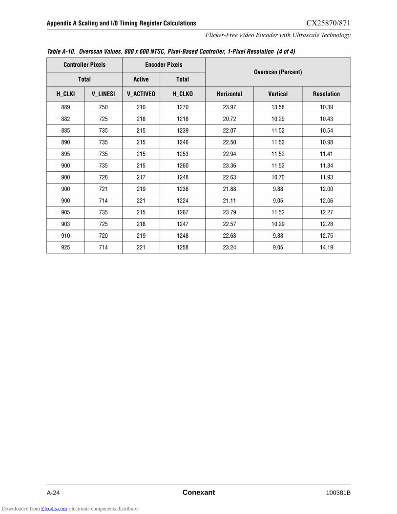
Appendix A Scaling and I/0 Timing Register Calculations CX25870/871
Flicker-Free Video Encoder with Ultrascale Technology
A-24 Conexant 100381B
889 750 210 1270 23.97 13.58 10.39
882 725 218 1218 20.72 10.29 10.43
885 735 215 1239 22.07 11.52 10.54
890 735 215 1246 22.50 11.52 10.98
895 735 215 1253 22.94 11.52 11.41
900 735 215 1260 23.36 11.52 11.84
900 728 217 1248 22.63 10.70 11.93
900 721 219 1236 21.88 9.88 12.00
900 714 221 1224 21.11 9.05 12.06
905 735 215 1267 23.79 11.52 12.27
903 725 218 1247 22.57 10.29 12.28
910 720 219 1248 22.63 9.88 12.75
925 714 221 1258 23.24 9.05 14.19
Table A-10. Overscan Values, 800 x 600 NTSC, Pixel-Based Controller, 1-Pixel Resolution (4 of 4)
Controller Pixels Encoder PixelsOverscan (Percent)
Total Active Total
H_CLKI V_LINESI V_ACTIVEO H_CLKO Horizontal Vertical Resolution
Downloaded from Elcodis.com electronic components distributor
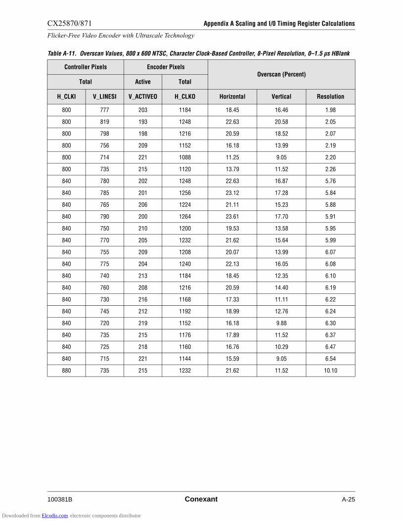
CX25870/871 Appendix A Scaling and I/0 Timing Register Calculations
Flicker-Free Video Encoder with Ultrascale Technology
100381B Conexant A-25
Table A-11. Overscan Values, 800 x 600 NTSC, Character Clock-Based Controller, 8-Pixel Resolution, 0–1.5 µs HBlank
Controller Pixels Encoder PixelsOverscan (Percent)
Total Active Total
H_CLKI V_LINESI V_ACTIVEO H_CLKO Horizontal Vertical Resolution
800 777 203 1184 18.45 16.46 1.98
800 819 193 1248 22.63 20.58 2.05
800 798 198 1216 20.59 18.52 2.07
800 756 209 1152 16.18 13.99 2.19
800 714 221 1088 11.25 9.05 2.20
800 735 215 1120 13.79 11.52 2.26
840 780 202 1248 22.63 16.87 5.76
840 785 201 1256 23.12 17.28 5.84
840 765 206 1224 21.11 15.23 5.88
840 790 200 1264 23.61 17.70 5.91
840 750 210 1200 19.53 13.58 5.95
840 770 205 1232 21.62 15.64 5.99
840 755 209 1208 20.07 13.99 6.07
840 775 204 1240 22.13 16.05 6.08
840 740 213 1184 18.45 12.35 6.10
840 760 208 1216 20.59 14.40 6.19
840 730 216 1168 17.33 11.11 6.22
840 745 212 1192 18.99 12.76 6.24
840 720 219 1152 16.18 9.88 6.30
840 735 215 1176 17.89 11.52 6.37
840 725 218 1160 16.76 10.29 6.47
840 715 221 1144 15.59 9.05 6.54
880 735 215 1232 21.62 11.52 10.10
Downloaded from Elcodis.com electronic components distributor
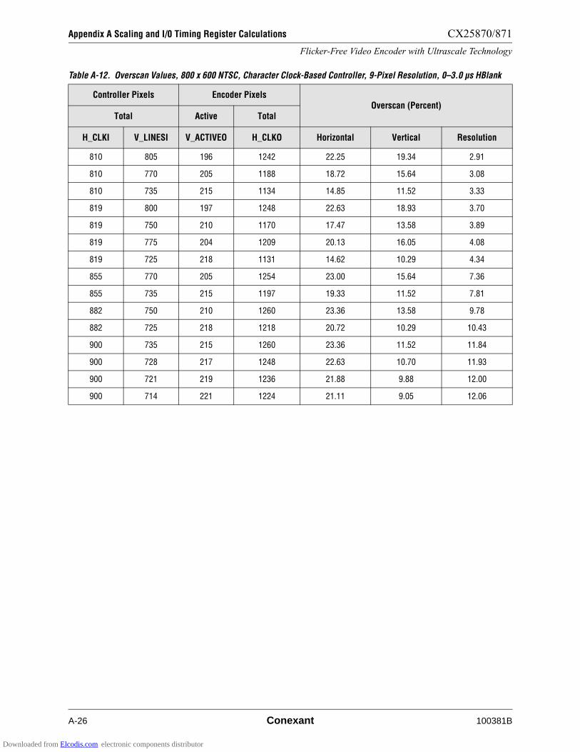
Appendix A Scaling and I/0 Timing Register Calculations CX25870/871
Flicker-Free Video Encoder with Ultrascale Technology
A-26 Conexant 100381B
Table A-12. Overscan Values, 800 x 600 NTSC, Character Clock-Based Controller, 9-Pixel Resolution, 0–3.0 µs HBlank
Controller Pixels Encoder PixelsOverscan (Percent)
Total Active Total
H_CLKI V_LINESI V_ACTIVEO H_CLKO Horizontal Vertical Resolution
810 805 196 1242 22.25 19.34 2.91
810 770 205 1188 18.72 15.64 3.08
810 735 215 1134 14.85 11.52 3.33
819 800 197 1248 22.63 18.93 3.70
819 750 210 1170 17.47 13.58 3.89
819 775 204 1209 20.13 16.05 4.08
819 725 218 1131 14.62 10.29 4.34
855 770 205 1254 23.00 15.64 7.36
855 735 215 1197 19.33 11.52 7.81
882 750 210 1260 23.36 13.58 9.78
882 725 218 1218 20.72 10.29 10.43
900 735 215 1260 23.36 11.52 11.84
900 728 217 1248 22.63 10.70 11.93
900 721 219 1236 21.88 9.88 12.00
900 714 221 1224 21.11 9.05 12.06
Downloaded from Elcodis.com electronic components distributor

CX25870/871 Appendix A Scaling and I/0 Timing Register Calculations
Flicker-Free Video Encoder with Ultrascale Technology
100381B Conexant A-27
Table A-13. Overscan Values 800 x 600 NTSC, Pixel-Based Controller, 1-Pixel Resolution, 3:2 Clocking Mode (1 of 4)
Controller Pixels Encoder PixelsOverscan (Percent)
Total Active Total
H_CLKI V_LINESI V_ACTIVEO H_CLKO Horizontal Vertical Delta
1170 770 205 1144 15.59 15.64 –0.04
1170 735 215 1092 11.57 11.52 0.05
1170 805 196 1196 19.26 19.34 –0.08
1176 750 210 1120 13.79 13.58 0.21
1176 825 191 1232 21.62 21.40 0.22
1175 756 209 1128 14.40 13.99 0.40
1175 819 193 1222 20.98 20.58 0.41
1155 795 199 1166 17.19 18.11 –0.92
1155 810 195 1188 18.72 19.75 –1.03
1155 735 215 1078 10.43 11.52 –1.10
1185 735 215 1106 12.69 11.52 1.17
1155 825 191 1210 20.20 21.40 –1.20
1190 765 206 1156 16.47 15.23 1.24
1155 780 202 1144 15.59 16.87 –1.28
1155 765 206 1122 13.94 15.23 –1.29
1150 819 193 1196 19.26 20.58 –1.31
1190 810 195 1224 21.11 19.75 1.36
1155 750 210 1100 12.22 13.58 –1.36
1190 720 219 1088 11.25 9.88 1.37
1150 756 209 1104 12.54 13.99 –1.46
1197 800 197 1216 20.59 18.93 1.66
1197 750 210 1140 15.30 13.58 1.72
1197 775 204 1178 18.03 16.05 1.98
1200 777 203 1184 18.45 16.46 1.98
1200 798 198 1216 20.59 18.52 2.07
1197 725 218 1102 12.38 10.29 2.09
1200 756 209 1152 16.18 13.99 2.19
1200 714 221 1088 11.25 9.05 2.20
1200 735 215 1120 13.79 11.52 2.26
1140 735 215 1064 9.25 11.52 –2.27
Downloaded from Elcodis.com electronic components distributor
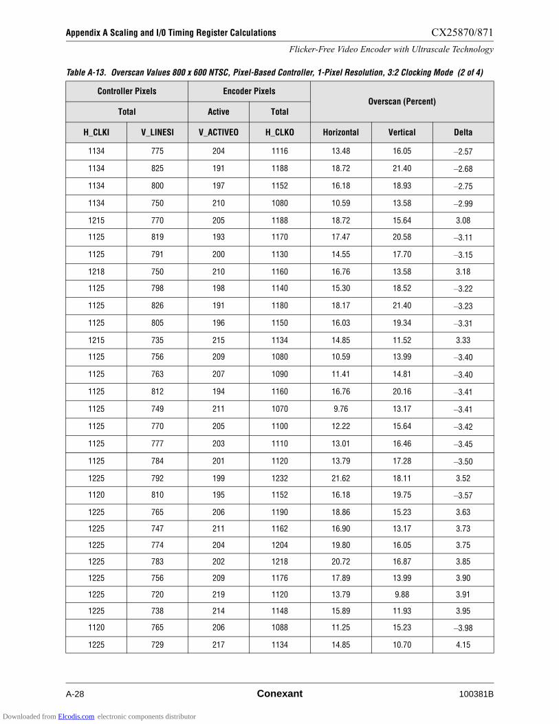
Appendix A Scaling and I/0 Timing Register Calculations CX25870/871
Flicker-Free Video Encoder with Ultrascale Technology
A-28 Conexant 100381B
1134 775 204 1116 13.48 16.05 –2.57
1134 825 191 1188 18.72 21.40 –2.68
1134 800 197 1152 16.18 18.93 –2.75
1134 750 210 1080 10.59 13.58 –2.99
1215 770 205 1188 18.72 15.64 3.08
1125 819 193 1170 17.47 20.58 –3.11
1125 791 200 1130 14.55 17.70 –3.15
1218 750 210 1160 16.76 13.58 3.18
1125 798 198 1140 15.30 18.52 –3.22
1125 826 191 1180 18.17 21.40 –3.23
1125 805 196 1150 16.03 19.34 –3.31
1215 735 215 1134 14.85 11.52 3.33
1125 756 209 1080 10.59 13.99 –3.40
1125 763 207 1090 11.41 14.81 –3.40
1125 812 194 1160 16.76 20.16 –3.41
1125 749 211 1070 9.76 13.17 –3.41
1125 770 205 1100 12.22 15.64 –3.42
1125 777 203 1110 13.01 16.46 –3.45
1125 784 201 1120 13.79 17.28 –3.50
1225 792 199 1232 21.62 18.11 3.52
1120 810 195 1152 16.18 19.75 –3.57
1225 765 206 1190 18.86 15.23 3.63
1225 747 211 1162 16.90 13.17 3.73
1225 774 204 1204 19.80 16.05 3.75
1225 783 202 1218 20.72 16.87 3.85
1225 756 209 1176 17.89 13.99 3.90
1225 720 219 1120 13.79 9.88 3.91
1225 738 214 1148 15.89 11.93 3.95
1120 765 206 1088 11.25 15.23 –3.98
1225 729 217 1134 14.85 10.70 4.15
Table A-13. Overscan Values 800 x 600 NTSC, Pixel-Based Controller, 1-Pixel Resolution, 3:2 Clocking Mode (2 of 4)
Controller Pixels Encoder PixelsOverscan (Percent)
Total Active Total
H_CLKI V_LINESI V_ACTIVEO H_CLKO Horizontal Vertical Delta
Downloaded from Elcodis.com electronic components distributor

CX25870/871 Appendix A Scaling and I/0 Timing Register Calculations
Flicker-Free Video Encoder with Ultrascale Technology
100381B Conexant A-29
1113 825 191 1166 17.19 21.40 –4.21
1230 735 215 1148 15.89 11.52 4.37
1239 750 210 1180 18.17 13.58 4.59
1100 819 193 1144 15.59 20.58 –4.98
1245 735 215 1162 16.90 11.52 5.38
1250 756 209 1200 19.53 13.99 5.54
1092 825 191 1144 15.59 21.40 –5.81
1260 765 206 1224 21.11 15.23 5.88
1260 750 210 1200 19.53 13.58 5.95
1260 770 205 1232 21.62 15.64 5.99
1260 755 209 1208 20.07 13.99 6.07
1260 740 213 1184 18.45 12.35 6.10
1260 760 208 1216 20.59 14.40 6.19
1260 730 216 1168 17.33 11.11 6.22
1260 745 212 1192 18.99 12.76 6.24
1085 810 195 1116 13.48 19.75 –6.28
1260 720 219 1152 16.18 9.88 6.30
1260 735 215 1176 17.89 11.52 6.37
1260 725 218 1160 16.76 10.29 6.47
1260 715 221 1144 15.59 9.05 6.54
1080 805 196 1104 12.54 19.34 –6.81
1075 819 193 1118 13.63 20.58 –6.95
1275 756 209 1224 21.11 13.99 7.12
1281 750 210 1220 20.85 13.58 7.27
1275 735 215 1190 18.86 11.52 7.33
1275 714 221 1156 16.47 9.05 7.42
1071 825 191 1122 13.94 21.40 –7.46
1071 800 197 1088 11.25 18.93 –7.68
1290 735 215 1204 19.80 11.52 8.28
1295 720 219 1184 18.45 9.88 8.57
1050 828 191 1104 12.54 21.40 –8.86
Table A-13. Overscan Values 800 x 600 NTSC, Pixel-Based Controller, 1-Pixel Resolution, 3:2 Clocking Mode (3 of 4)
Controller Pixels Encoder PixelsOverscan (Percent)
Total Active Total
H_CLKI V_LINESI V_ACTIVEO H_CLKO Horizontal Vertical Delta
Downloaded from Elcodis.com electronic components distributor
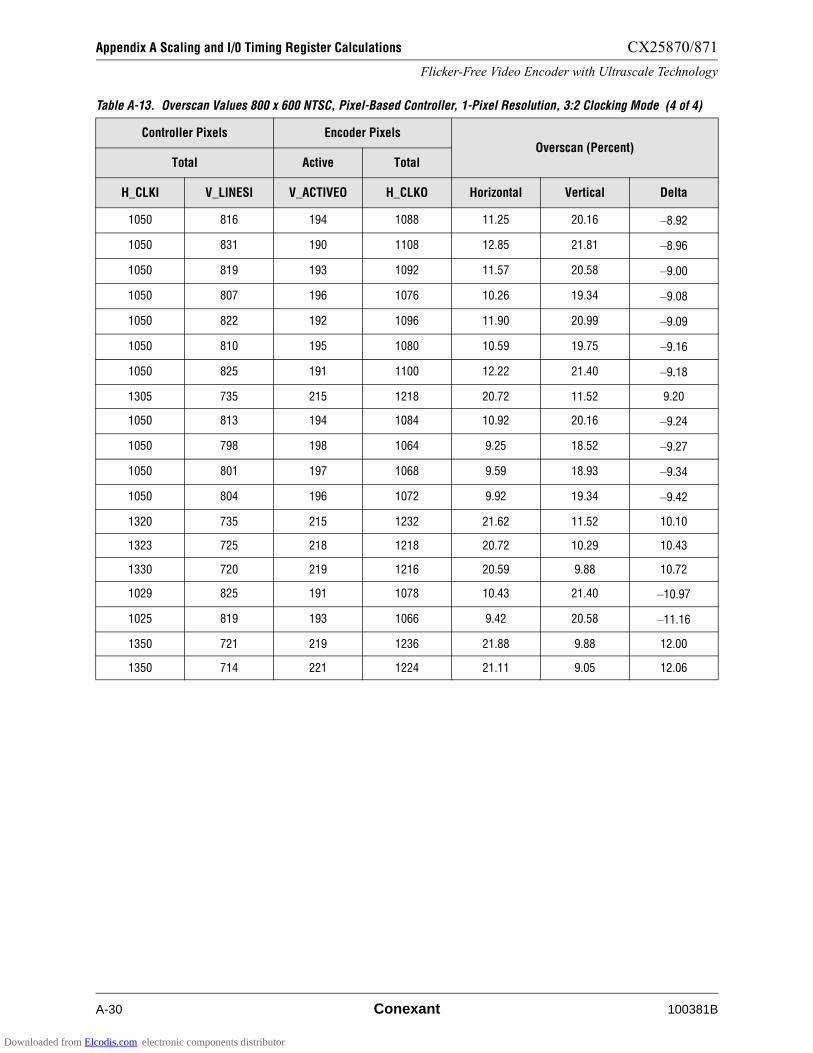
Appendix A Scaling and I/0 Timing Register Calculations CX25870/871
Flicker-Free Video Encoder with Ultrascale Technology
A-30 Conexant 100381B
1050 816 194 1088 11.25 20.16 –8.92
1050 831 190 1108 12.85 21.81 –8.96
1050 819 193 1092 11.57 20.58 –9.00
1050 807 196 1076 10.26 19.34 –9.08
1050 822 192 1096 11.90 20.99 –9.09
1050 810 195 1080 10.59 19.75 –9.16
1050 825 191 1100 12.22 21.40 –9.18
1305 735 215 1218 20.72 11.52 9.20
1050 813 194 1084 10.92 20.16 –9.24
1050 798 198 1064 9.25 18.52 –9.27
1050 801 197 1068 9.59 18.93 –9.34
1050 804 196 1072 9.92 19.34 –9.42
1320 735 215 1232 21.62 11.52 10.10
1323 725 218 1218 20.72 10.29 10.43
1330 720 219 1216 20.59 9.88 10.72
1029 825 191 1078 10.43 21.40 –10.97
1025 819 193 1066 9.42 20.58 –11.16
1350 721 219 1236 21.88 9.88 12.00
1350 714 221 1224 21.11 9.05 12.06
Table A-13. Overscan Values 800 x 600 NTSC, Pixel-Based Controller, 1-Pixel Resolution, 3:2 Clocking Mode (4 of 4)
Controller Pixels Encoder PixelsOverscan (Percent)
Total Active Total
H_CLKI V_LINESI V_ACTIVEO H_CLKO Horizontal Vertical Delta
Downloaded from Elcodis.com electronic components distributor
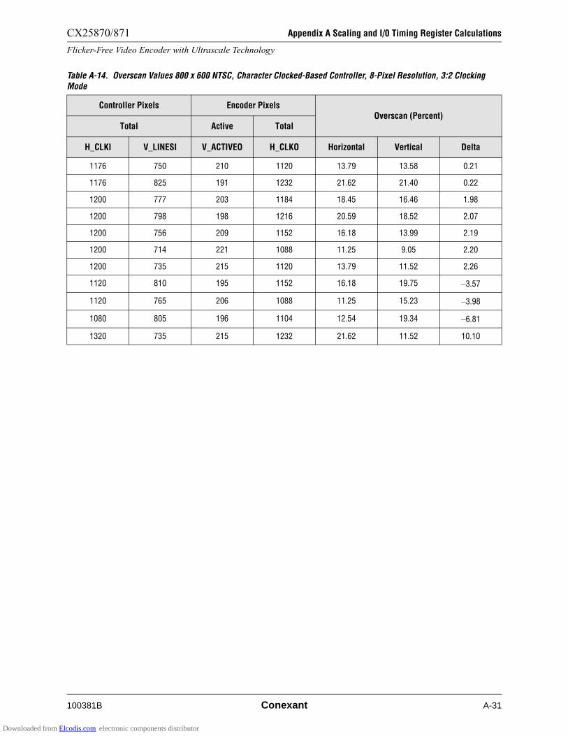
CX25870/871 Appendix A Scaling and I/0 Timing Register Calculations
Flicker-Free Video Encoder with Ultrascale Technology
100381B Conexant A-31
Table A-14. Overscan Values 800 x 600 NTSC, Character Clocked-Based Controller, 8-Pixel Resolution, 3:2 Clocking Mode
Controller Pixels Encoder PixelsOverscan (Percent)
Total Active Total
H_CLKI V_LINESI V_ACTIVEO H_CLKO Horizontal Vertical Delta
1176 750 210 1120 13.79 13.58 0.21
1176 825 191 1232 21.62 21.40 0.22
1200 777 203 1184 18.45 16.46 1.98
1200 798 198 1216 20.59 18.52 2.07
1200 756 209 1152 16.18 13.99 2.19
1200 714 221 1088 11.25 9.05 2.20
1200 735 215 1120 13.79 11.52 2.26
1120 810 195 1152 16.18 19.75 –3.57
1120 765 206 1088 11.25 15.23 –3.98
1080 805 196 1104 12.54 19.34 –6.81
1320 735 215 1232 21.62 11.52 10.10
Downloaded from Elcodis.com electronic components distributor

Appendix A Scaling and I/0 Timing Register Calculations CX25870/871
Flicker-Free Video Encoder with Ultrascale Technology
A-32 Conexant 100381B
Table A-15. Overscan Values 800 x 600 NTSC, Character Clocked-Based Controller, 9-Pixel Resolution, 3:2 Clocking Mode (1 of 2)
Controller Pixels Encoder PixelsOverscan (Percent)
Total Active Total
H_CLKI V_LINESI V_ACTIVEO H_CLKO Horizontal Vertical Delta
1170 770 205 1144 15.59 15.64 –0.04
1170 735 215 1092 11.57 11.52 0.05
1170 805 196 1196 19.26 19.34 –0.08
1197 800 197 1216 20.59 18.93 1.66
1197 750 210 1140 15.30 13.58 1.72
1197 775 204 1178 18.03 16.05 1.98
1197 725 218 1102 12.38 10.29 2.09
1134 775 204 1116 13.48 16.05 –2.57
1134 825 191 1188 18.72 21.40 –2.68
1134 800 197 1152 16.18 18.93 –2.75
1134 750 210 1080 10.59 13.58 –2.99
1215 770 205 1188 18.72 15.64 3.08
1125 819 193 1170 17.47 20.58 –3.11
1125 791 200 1130 14.55 17.70 –3.15
1125 798 198 1140 15.30 18.52 –3.22
1125 826 191 1180 18.17 21.40 –3.23
1125 805 196 1150 16.03 19.34 –3.31
1215 735 215 1134 14.85 11.52 3.33
1125 756 209 1080 10.59 13.99 –3.40
1125 763 207 1090 11.41 14.81 –3.40
1125 812 194 1160 16.76 20.16 –3.41
1125 749 211 1070 9.76 13.17 –3.41
1125 770 205 1100 12.22 15.64 –3.42
1125 777 203 1110 13.01 16.46 –3.45
1125 784 201 1120 13.79 17.28 –3.50
1260 765 206 1224 21.11 15.23 5.88
1260 750 210 1200 19.53 13.58 5.95
1260 770 205 1232 21.62 15.64 5.99
1260 755 209 1208 20.07 13.99 6.07
1260 740 213 1184 18.45 12.35 6.10
Downloaded from Elcodis.com electronic components distributor
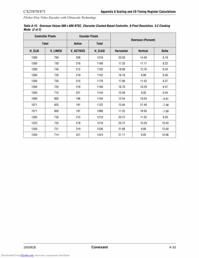
CX25870/871 Appendix A Scaling and I/0 Timing Register Calculations
Flicker-Free Video Encoder with Ultrascale Technology
100381B Conexant A-33
1260 760 208 1216 20.59 14.40 6.19
1260 730 216 1168 17.33 11.11 6.22
1260 745 212 1192 18.99 12.76 6.24
1260 720 219 1152 16.18 9.88 6.30
1260 735 215 1176 17.89 11.52 6.37
1260 725 218 1160 16.76 10.29 6.47
1260 715 221 1144 15.59 9.05 6.54
1080 805 196 1104 12.54 19.34 –6.81
1071 825 191 1122 13.94 21.40 –7.46
1071 800 197 1088 11.25 18.93 –7.68
1305 735 215 1218 20.72 11.52 9.20
1323 725 218 1218 20.72 10.29 10.43
1350 721 219 1236 21.88 9.88 12.00
1350 714 221 1224 21.11 9.05 12.06
Table A-15. Overscan Values 800 x 600 NTSC, Character Clocked-Based Controller, 9-Pixel Resolution, 3:2 Clocking Mode (2 of 2)
Controller Pixels Encoder PixelsOverscan (Percent)
Total Active Total
H_CLKI V_LINESI V_ACTIVEO H_CLKO Horizontal Vertical Delta
Downloaded from Elcodis.com electronic components distributor

Appendix A Scaling and I/0 Timing Register Calculations CX25870/871
Flicker-Free Video Encoder with Ultrascale Technology
A-34 Conexant 100381B
Table A-16. Overscan Values, 800 x 600 PAL-BDGHI, Pixel-Based Controller, 1-Pixel Resolution, >2.5 µs HBlank (1 of 2)
Controller Pixels Encoder PixelsOverscan (Percent)
Total Active Total
H_CLKI V_LINESI V_ACTIVEO H_CLKO Horizontal Vertical Resolution
945 750 250 1134 13.17 13.19 –0.02
950 750 250 1140 13.63 13.19 0.44
950 775 242 1178 16.42 15.97 0.44
940 750 250 1128 12.71 13.19 –0.48
950 725 259 1102 10.65 10.07 0.58
950 800 235 1216 19.03 18.40 0.63
950 825 228 1254 21.48 20.83 0.65
955 750 250 1146 14.08 13.19 0.89
935 750 250 1122 12.24 13.19 –0.95
960 750 250 1152 14.53 13.19 1.34
930 750 250 1116 11.77 13.19 –1.42
925 825 228 1221 19.36 20.83 –1.47
925 800 235 1184 16.84 18.40 –1.56
965 750 250 1158 14.97 13.19 1.78
925 775 242 1147 14.16 15.97 –1.81
925 750 250 1110 11.30 13.19 –1.90
970 750 250 1164 15.41 13.19 2.22
920 750 250 1104 10.81 13.19 –2.38
975 775 242 1209 18.56 15.97 2.59
975 750 250 1170 15.84 13.19 2.65
975 800 235 1248 21.10 18.40 2.70
915 750 250 1098 10.33 13.19 –2.87
975 725 259 1131 12.94 10.07 2.87
980 750 250 1176 16.27 13.19 3.08
910 750 250 1092 9.83 13.19 –3.36
985 750 250 1182 16.70 13.19 3.50
900 825 228 1188 17.12 20.83 –3.71
905 750 250 1086 9.34 13.19 –3.86
900 800 235 1152 14.53 18.40 –3.87
990 750 250 1188 17.12 13.19 3.93
900 775 242 1116 11.77 15.97 –4.20
Downloaded from Elcodis.com electronic components distributor
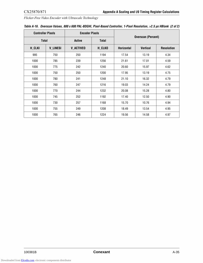
CX25870/871 Appendix A Scaling and I/0 Timing Register Calculations
Flicker-Free Video Encoder with Ultrascale Technology
100381B Conexant A-35
995 750 250 1194 17.54 13.19 4.34
1000 785 239 1256 21.61 17.01 4.59
1000 775 242 1240 20.60 15.97 4.62
1000 750 250 1200 17.95 13.19 4.75
1000 780 241 1248 21.10 16.32 4.79
1000 760 247 1216 19.03 14.24 4.79
1000 770 244 1232 20.08 15.28 4.80
1000 745 252 1192 17.40 12.50 4.90
1000 730 257 1168 15.70 10.76 4.94
1000 755 249 1208 18.49 13.54 4.95
1000 765 246 1224 19.56 14.58 4.97
Table A-16. Overscan Values, 800 x 600 PAL-BDGHI, Pixel-Based Controller, 1-Pixel Resolution, >2.5 µs HBlank (2 of 2)
Controller Pixels Encoder PixelsOverscan (Percent)
Total Active Total
H_CLKI V_LINESI V_ACTIVEO H_CLKO Horizontal Vertical Resolution
Downloaded from Elcodis.com electronic components distributor
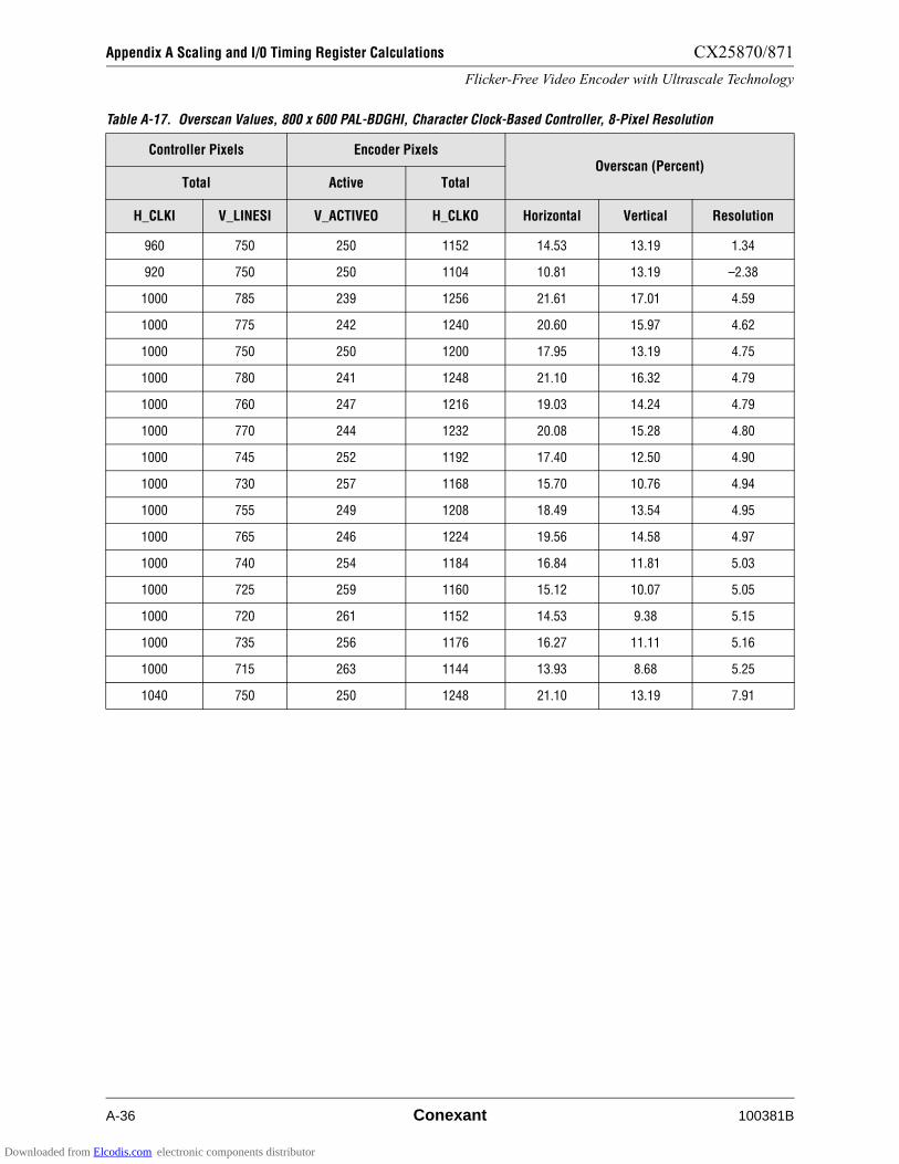
Appendix A Scaling and I/0 Timing Register Calculations CX25870/871
Flicker-Free Video Encoder with Ultrascale Technology
A-36 Conexant 100381B
Table A-17. Overscan Values, 800 x 600 PAL-BDGHI, Character Clock-Based Controller, 8-Pixel Resolution
Controller Pixels Encoder PixelsOverscan (Percent)
Total Active Total
H_CLKI V_LINESI V_ACTIVEO H_CLKO Horizontal Vertical Resolution
960 750 250 1152 14.53 13.19 1.34
920 750 250 1104 10.81 13.19 –2.38
1000 785 239 1256 21.61 17.01 4.59
1000 775 242 1240 20.60 15.97 4.62
1000 750 250 1200 17.95 13.19 4.75
1000 780 241 1248 21.10 16.32 4.79
1000 760 247 1216 19.03 14.24 4.79
1000 770 244 1232 20.08 15.28 4.80
1000 745 252 1192 17.40 12.50 4.90
1000 730 257 1168 15.70 10.76 4.94
1000 755 249 1208 18.49 13.54 4.95
1000 765 246 1224 19.56 14.58 4.97
1000 740 254 1184 16.84 11.81 5.03
1000 725 259 1160 15.12 10.07 5.05
1000 720 261 1152 14.53 9.38 5.15
1000 735 256 1176 16.27 11.11 5.16
1000 715 263 1144 13.93 8.68 5.25
1040 750 250 1248 21.10 13.19 7.91
Downloaded from Elcodis.com electronic components distributor

CX25870/871 Appendix A Scaling and I/0 Timing Register Calculations
Flicker-Free Video Encoder with Ultrascale Technology
100381B Conexant A-37
Table A-18. Overscan Values, 800 x 600 PAL-BDGHI, Character Clock-Based Controller, 9-Pixel Resolution
Controller Pixels Encoder PixelsOverscan (Percent)
Total Active Total
H_CLKI V_LINESI V_ACTIVEO H_CLKO Horizontal Vertical Resolution
945 750 250 1134 13.17 13.19 –0.02
900 825 228 1188 17.12 20.83 –3.71
900 800 235 1152 14.53 18.40 –3.87
990 750 250 1188 17.12 13.19 3.93
900 775 242 1116 11.77 15.97 –4.20
1035 750 250 1242 20.72 13.19 7.53
Downloaded from Elcodis.com electronic components distributor

Appendix A Scaling and I/0 Timing Register Calculations CX25870/871
Flicker-Free Video Encoder with Ultrascale Technology
A-38 Conexant 100381B
Table A-19. Overscan Values 800 x 600 PAL-BDGHI, Pixel-Based Controller, 1-Pixel Resolution, 3:2 Clocking Mode (1 of 3)
Controller Pixels Encoder PixelsOverscan (Percent)
Total Active Total
H_CLKI V_LINESI V_ACTIVEO H_CLKO Horizontal Vertical Delta
1420 750 250 1136 13.33 13.19 0.13
1415 750 250 1132 13.02 13.19 –0.17
1425 750 250 1140 13.63 13.19 0.44
1425 775 242 1178 16.42 15.97 0.44
1410 750 250 1128 12.71 13.19 –0.48
1425 725 259 1102 10.65 10.07 0.58
1425 800 235 1216 19.03 18.40 0.63
1425 825 228 1254 21.48 20.83 0.65
1430 750 250 1144 13.93 13.19 0.74
1400 825 228 1232 20.08 20.83 –0.75
1405 750 250 1124 12.40 13.19 –0.79
1435 750 250 1148 14.23 13.19 1.04
1400 750 250 1120 12.09 13.19 –1.11
1440 750 250 1152 14.53 13.19 1.34
1395 750 250 1116 11.77 13.19 –1.42
1445 750 250 1156 14.83 13.19 1.63
1390 750 250 1112 11.46 13.19 –1.74
1450 750 250 1160 15.12 13.19 1.92
1385 750 250 1108 11.14 13.19 –2.06
1375 825 228 1210 18.63 20.83 –2.21
1455 750 250 1164 15.41 13.19 2.22
1375 810 232 1188 17.12 19.44 –2.32
1375 765 246 1122 12.24 14.58 –2.34
1380 750 250 1104 10.81 13.19 –2.38
1375 780 241 1144 13.93 16.32 –2.39
1375 795 236 1166 15.56 18.06 –2.50
1460 750 250 1168 15.70 13.19 2.51
1375 750 250 1100 10.49 13.19 –2.70
1465 750 250 1172 15.99 13.19 2.79
1370 750 250 1096 10.16 13.19 –3.03
Downloaded from Elcodis.com electronic components distributor

CX25870/871 Appendix A Scaling and I/0 Timing Register Calculations
Flicker-Free Video Encoder with Ultrascale Technology
100381B Conexant A-39
1470 750 250 1176 16.27 13.19 3.08
1365 750 250 1092 9.83 13.19 –3.36
1475 750 250 1180 16.56 13.19 3.36
1480 750 250 1184 16.84 13.19 3.65
1360 750 250 1088 9.50 13.19 –3.69
1350 825 228 1188 17.12 20.83 –3.71
1350 800 235 1152 14.53 18.40 –3.87
1485 750 250 1188 17.12 13.19 3.93
1355 750 250 1084 9.17 13.19 –4.03
1350 775 242 1116 11.77 15.97 –4.20
1490 750 250 1192 17.40 13.19 4.20
1495 750 250 1196 17.67 13.19 4.48
1500 785 239 1256 21.61 17.01 4.59
1500 775 242 1240 20.60 15.97 4.62
1500 750 250 1200 17.95 13.19 4.75
1500 780 241 1248 21.10 16.32 4.79
1500 760 247 1216 19.03 14.24 4.79
1500 770 244 1232 20.08 15.28 4.80
1500 745 252 1192 17.40 12.50 4.90
1500 730 257 1168 15.70 10.76 4.94
1500 755 249 1208 18.49 13.54 4.95
1500 765 246 1224 19.56 14.58 4.97
1505 750 250 1204 18.22 13.19 5.03
1500 740 254 1184 16.84 11.81 5.03
1500 725 259 1160 15.12 10.07 5.05
1500 720 261 1152 14.53 9.38 5.15
1500 735 256 1176 16.27 11.11 5.16
1500 715 263 1144 13.93 8.68 5.25
1325 825 228 1166 15.56 20.83 –5.28
1510 750 250 1208 18.49 13.19 5.30
Table A-19. Overscan Values 800 x 600 PAL-BDGHI, Pixel-Based Controller, 1-Pixel Resolution, 3:2 Clocking Mode (2 of 3)
Controller Pixels Encoder PixelsOverscan (Percent)
Total Active Total
H_CLKI V_LINESI V_ACTIVEO H_CLKO Horizontal Vertical Delta
Downloaded from Elcodis.com electronic components distributor
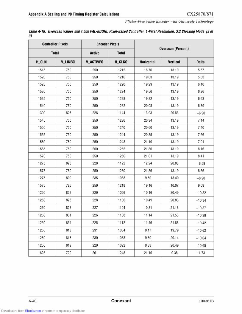
Appendix A Scaling and I/0 Timing Register Calculations CX25870/871
Flicker-Free Video Encoder with Ultrascale Technology
A-40 Conexant 100381B
1515 750 250 1212 18.76 13.19 5.57
1520 750 250 1216 19.03 13.19 5.83
1525 750 250 1220 19.29 13.19 6.10
1530 750 250 1224 19.56 13.19 6.36
1535 750 250 1228 19.82 13.19 6.63
1540 750 250 1232 20.08 13.19 6.89
1300 825 228 1144 13.93 20.83 –6.90
1545 750 250 1236 20.34 13.19 7.14
1550 750 250 1240 20.60 13.19 7.40
1555 750 250 1244 20.85 13.19 7.66
1560 750 250 1248 21.10 13.19 7.91
1565 750 250 1252 21.36 13.19 8.16
1570 750 250 1256 21.61 13.19 8.41
1275 825 228 1122 12.24 20.83 –8.59
1575 750 250 1260 21.86 13.19 8.66
1275 800 235 1088 9.50 18.40 –8.90
1575 725 259 1218 19.16 10.07 9.09
1250 822 229 1096 10.16 20.49 –10.32
1250 825 228 1100 10.49 20.83 –10.34
1250 828 227 1104 10.81 21.18 –10.37
1250 831 226 1108 11.14 21.53 –10.39
1250 834 225 1112 11.46 21.88 –10.42
1250 813 231 1084 9.17 19.79 –10.62
1250 816 230 1088 9.50 20.14 –10.64
1250 819 229 1092 9.83 20.49 –10.65
1625 720 261 1248 21.10 9.38 11.73
Table A-19. Overscan Values 800 x 600 PAL-BDGHI, Pixel-Based Controller, 1-Pixel Resolution, 3:2 Clocking Mode (3 of 3)
Controller Pixels Encoder PixelsOverscan (Percent)
Total Active Total
H_CLKI V_LINESI V_ACTIVEO H_CLKO Horizontal Vertical Delta
Downloaded from Elcodis.com electronic components distributor
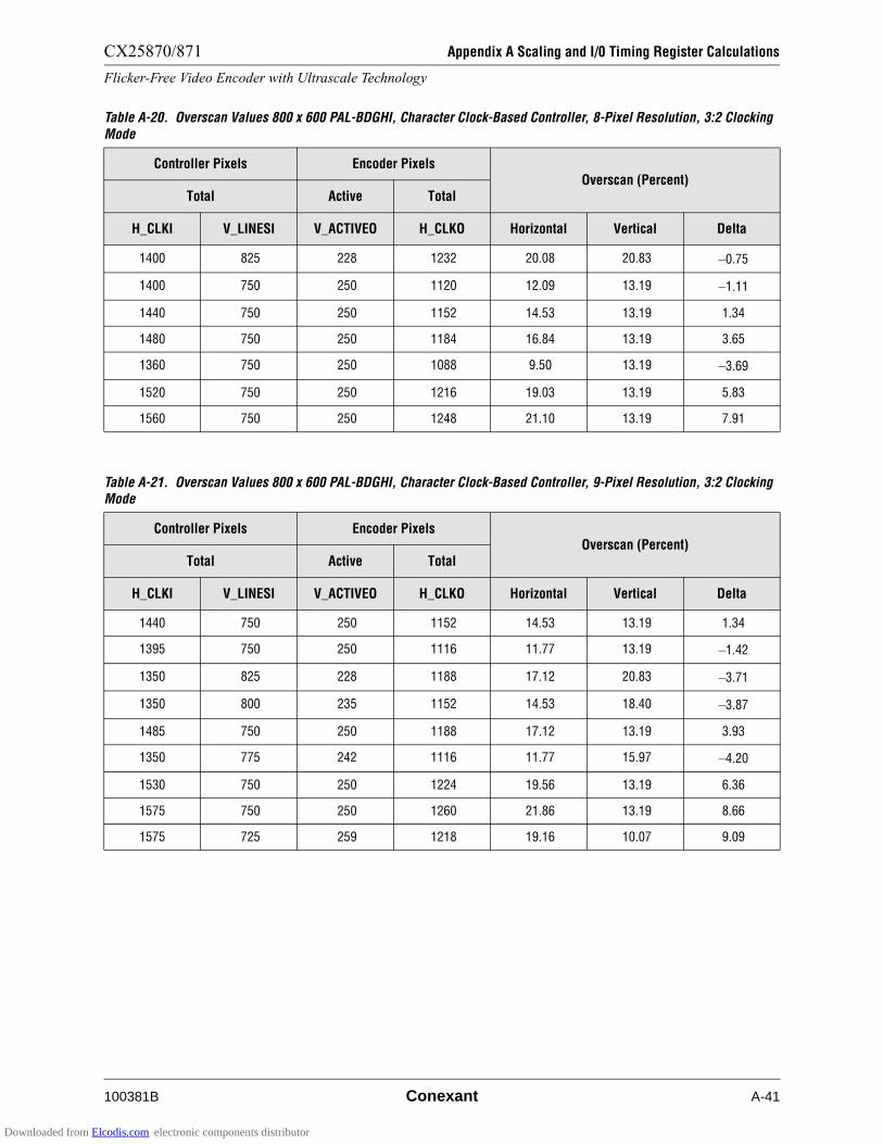
CX25870/871 Appendix A Scaling and I/0 Timing Register Calculations
Flicker-Free Video Encoder with Ultrascale Technology
100381B Conexant A-41
Table A-20. Overscan Values 800 x 600 PAL-BDGHI, Character Clock-Based Controller, 8-Pixel Resolution, 3:2 Clocking Mode
Controller Pixels Encoder PixelsOverscan (Percent)
Total Active Total
H_CLKI V_LINESI V_ACTIVEO H_CLKO Horizontal Vertical Delta
1400 825 228 1232 20.08 20.83 –0.75
1400 750 250 1120 12.09 13.19 –1.11
1440 750 250 1152 14.53 13.19 1.34
1480 750 250 1184 16.84 13.19 3.65
1360 750 250 1088 9.50 13.19 –3.69
1520 750 250 1216 19.03 13.19 5.83
1560 750 250 1248 21.10 13.19 7.91
Table A-21. Overscan Values 800 x 600 PAL-BDGHI, Character Clock-Based Controller, 9-Pixel Resolution, 3:2 Clocking Mode
Controller Pixels Encoder PixelsOverscan (Percent)
Total Active Total
H_CLKI V_LINESI V_ACTIVEO H_CLKO Horizontal Vertical Delta
1440 750 250 1152 14.53 13.19 1.34
1395 750 250 1116 11.77 13.19 –1.42
1350 825 228 1188 17.12 20.83 –3.71
1350 800 235 1152 14.53 18.40 –3.87
1485 750 250 1188 17.12 13.19 3.93
1350 775 242 1116 11.77 15.97 –4.20
1530 750 250 1224 19.56 13.19 6.36
1575 750 250 1260 21.86 13.19 8.66
1575 725 259 1218 19.16 10.07 9.09
Downloaded from Elcodis.com electronic components distributor
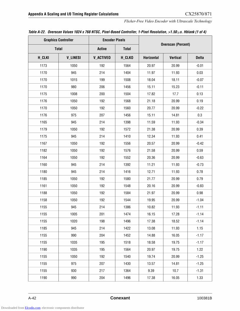
Appendix A Scaling and I/0 Timing Register Calculations CX25870/871
Flicker-Free Video Encoder with Ultrascale Technology
A-42 Conexant 100381B
Table A-22. Overscan Values 1024 x 768 NTSC, Pixel-Based Controller, 1-Pixel Resolution, >1.50 !s. Hblank (1 of 4)
Graphics Controller Encoder PixelsOverscan (Percent)
Total Active Total
H_CLKI V_LINESI V_ACTIVEO H_CLKO Horizontal Vertical Delta
1173 1050 192 1564 20.97 20.99 -0.01
1170 945 214 1404 11.97 11.93 0.03
1170 1015 199 1508 18.04 18.11 -0.07
1170 980 206 1456 15.11 15.23 -0.11
1175 1008 200 1504 17.82 17.7 0.13
1176 1050 192 1568 21.18 20.99 0.19
1170 1050 192 1560 20.77 20.99 -0.22
1176 975 207 1456 15.11 14.81 0.3
1165 945 214 1398 11.59 11.93 -0.34
1179 1050 192 1572 21.38 20.99 0.39
1175 945 214 1410 12.34 11.93 0.41
1167 1050 192 1556 20.57 20.99 -0.42
1182 1050 192 1576 21.58 20.99 0.59
1164 1050 192 1552 20.36 20.99 -0.63
1160 945 214 1392 11.21 11.93 -0.73
1180 945 214 1416 12.71 11.93 0.78
1185 1050 192 1580 21.77 20.99 0.79
1161 1050 192 1548 20.16 20.99 -0.83
1188 1050 192 1584 21.97 20.99 0.98
1158 1050 192 1544 19.95 20.99 -1.04
1155 945 214 1386 10.82 11.93 -1.11
1155 1005 201 1474 16.15 17.28 -1.14
1155 1020 198 1496 17.38 18.52 -1.14
1185 945 214 1422 13.08 11.93 1.15
1155 990 204 1452 14.88 16.05 -1.17
1155 1035 195 1518 18.58 19.75 -1.17
1190 1035 195 1564 20.97 19.75 1.22
1155 1050 192 1540 19.74 20.99 -1.25
1155 975 207 1430 13.57 14.81 -1.25
1155 930 217 1364 9.39 10.7 -1.31
1190 990 204 1496 17.38 16.05 1.33
Downloaded from Elcodis.com electronic components distributor
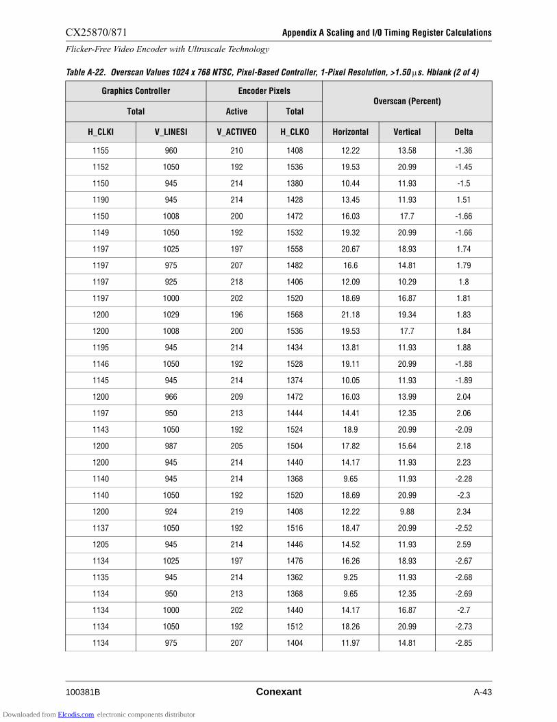
CX25870/871 Appendix A Scaling and I/0 Timing Register Calculations
Flicker-Free Video Encoder with Ultrascale Technology
100381B Conexant A-43
1155 960 210 1408 12.22 13.58 -1.36
1152 1050 192 1536 19.53 20.99 -1.45
1150 945 214 1380 10.44 11.93 -1.5
1190 945 214 1428 13.45 11.93 1.51
1150 1008 200 1472 16.03 17.7 -1.66
1149 1050 192 1532 19.32 20.99 -1.66
1197 1025 197 1558 20.67 18.93 1.74
1197 975 207 1482 16.6 14.81 1.79
1197 925 218 1406 12.09 10.29 1.8
1197 1000 202 1520 18.69 16.87 1.81
1200 1029 196 1568 21.18 19.34 1.83
1200 1008 200 1536 19.53 17.7 1.84
1195 945 214 1434 13.81 11.93 1.88
1146 1050 192 1528 19.11 20.99 -1.88
1145 945 214 1374 10.05 11.93 -1.89
1200 966 209 1472 16.03 13.99 2.04
1197 950 213 1444 14.41 12.35 2.06
1143 1050 192 1524 18.9 20.99 -2.09
1200 987 205 1504 17.82 15.64 2.18
1200 945 214 1440 14.17 11.93 2.23
1140 945 214 1368 9.65 11.93 -2.28
1140 1050 192 1520 18.69 20.99 -2.3
1200 924 219 1408 12.22 9.88 2.34
1137 1050 192 1516 18.47 20.99 -2.52
1205 945 214 1446 14.52 11.93 2.59
1134 1025 197 1476 16.26 18.93 -2.67
1135 945 214 1362 9.25 11.93 -2.68
1134 950 213 1368 9.65 12.35 -2.69
1134 1000 202 1440 14.17 16.87 -2.7
1134 1050 192 1512 18.26 20.99 -2.73
1134 975 207 1404 11.97 14.81 -2.85
Table A-22. Overscan Values 1024 x 768 NTSC, Pixel-Based Controller, 1-Pixel Resolution, >1.50 !s. Hblank (2 of 4)
Graphics Controller Encoder PixelsOverscan (Percent)
Total Active Total
H_CLKI V_LINESI V_ACTIVEO H_CLKO Horizontal Vertical Delta
Downloaded from Elcodis.com electronic components distributor
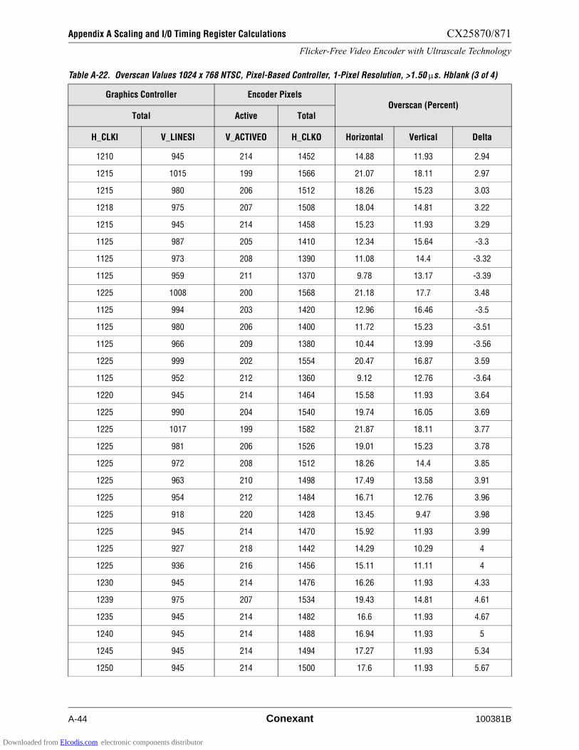
Appendix A Scaling and I/0 Timing Register Calculations CX25870/871
Flicker-Free Video Encoder with Ultrascale Technology
A-44 Conexant 100381B
1210 945 214 1452 14.88 11.93 2.94
1215 1015 199 1566 21.07 18.11 2.97
1215 980 206 1512 18.26 15.23 3.03
1218 975 207 1508 18.04 14.81 3.22
1215 945 214 1458 15.23 11.93 3.29
1125 987 205 1410 12.34 15.64 -3.3
1125 973 208 1390 11.08 14.4 -3.32
1125 959 211 1370 9.78 13.17 -3.39
1225 1008 200 1568 21.18 17.7 3.48
1125 994 203 1420 12.96 16.46 -3.5
1125 980 206 1400 11.72 15.23 -3.51
1125 966 209 1380 10.44 13.99 -3.56
1225 999 202 1554 20.47 16.87 3.59
1125 952 212 1360 9.12 12.76 -3.64
1220 945 214 1464 15.58 11.93 3.64
1225 990 204 1540 19.74 16.05 3.69
1225 1017 199 1582 21.87 18.11 3.77
1225 981 206 1526 19.01 15.23 3.78
1225 972 208 1512 18.26 14.4 3.85
1225 963 210 1498 17.49 13.58 3.91
1225 954 212 1484 16.71 12.76 3.96
1225 918 220 1428 13.45 9.47 3.98
1225 945 214 1470 15.92 11.93 3.99
1225 927 218 1442 14.29 10.29 4
1225 936 216 1456 15.11 11.11 4
1230 945 214 1476 16.26 11.93 4.33
1239 975 207 1534 19.43 14.81 4.61
1235 945 214 1482 16.6 11.93 4.67
1240 945 214 1488 16.94 11.93 5
1245 945 214 1494 17.27 11.93 5.34
1250 945 214 1500 17.6 11.93 5.67
Table A-22. Overscan Values 1024 x 768 NTSC, Pixel-Based Controller, 1-Pixel Resolution, >1.50 !s. Hblank (3 of 4)
Graphics Controller Encoder PixelsOverscan (Percent)
Total Active Total
H_CLKI V_LINESI V_ACTIVEO H_CLKO Horizontal Vertical Delta
Downloaded from Elcodis.com electronic components distributor
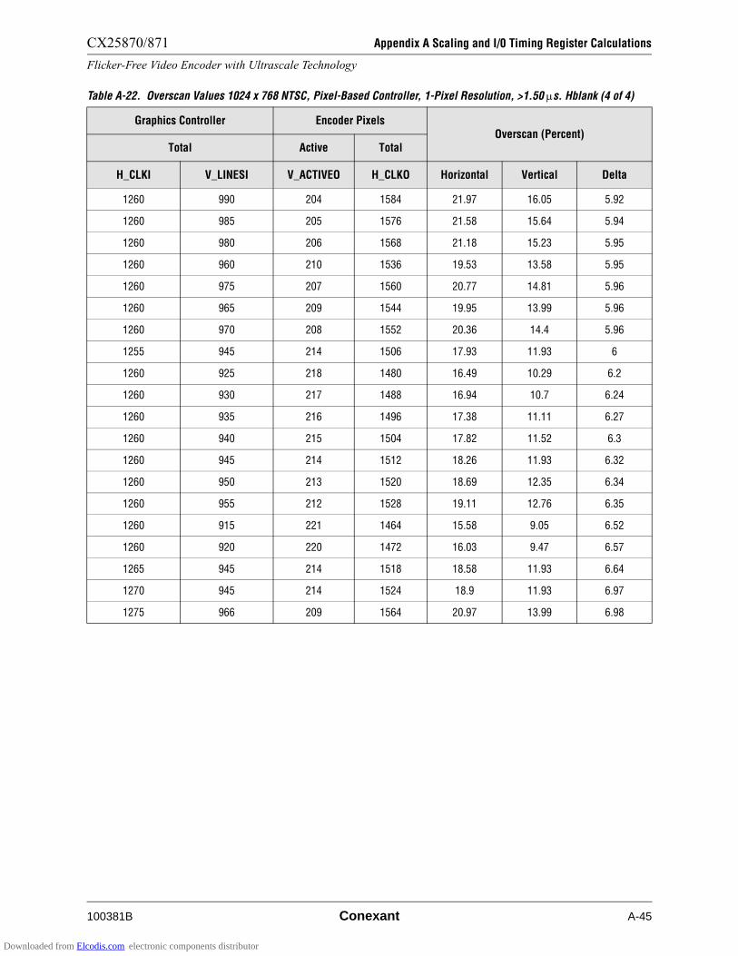
CX25870/871 Appendix A Scaling and I/0 Timing Register Calculations
Flicker-Free Video Encoder with Ultrascale Technology
100381B Conexant A-45
1260 990 204 1584 21.97 16.05 5.92
1260 985 205 1576 21.58 15.64 5.94
1260 980 206 1568 21.18 15.23 5.95
1260 960 210 1536 19.53 13.58 5.95
1260 975 207 1560 20.77 14.81 5.96
1260 965 209 1544 19.95 13.99 5.96
1260 970 208 1552 20.36 14.4 5.96
1255 945 214 1506 17.93 11.93 6
1260 925 218 1480 16.49 10.29 6.2
1260 930 217 1488 16.94 10.7 6.24
1260 935 216 1496 17.38 11.11 6.27
1260 940 215 1504 17.82 11.52 6.3
1260 945 214 1512 18.26 11.93 6.32
1260 950 213 1520 18.69 12.35 6.34
1260 955 212 1528 19.11 12.76 6.35
1260 915 221 1464 15.58 9.05 6.52
1260 920 220 1472 16.03 9.47 6.57
1265 945 214 1518 18.58 11.93 6.64
1270 945 214 1524 18.9 11.93 6.97
1275 966 209 1564 20.97 13.99 6.98
Table A-22. Overscan Values 1024 x 768 NTSC, Pixel-Based Controller, 1-Pixel Resolution, >1.50 !s. Hblank (4 of 4)
Graphics Controller Encoder PixelsOverscan (Percent)
Total Active Total
H_CLKI V_LINESI V_ACTIVEO H_CLKO Horizontal Vertical Delta
Downloaded from Elcodis.com electronic components distributor

Appendix A Scaling and I/0 Timing Register Calculations CX25870/871
Flicker-Free Video Encoder with Ultrascale Technology
A-46 Conexant 100381B
Table A-23. Overscan Values 1024 x 768 NTSC, Character Clock-Based Controller, 8-Pixel Resolution, >1.50 µs HBlank
Controller Pixels Encoder PixelsOverscan (Percent)
Total Active Total
H_CLKI V_LINESI V_ACTIVEO H_CLKO Horizontal Vertical Delta
1176 1050 192 1568 21.18 20.99 0.19
1176 975 207 1456 15.11 14.81 0.30
1160 945 214 1392 11.21 11.93 –0.73
1152 1050 192 1536 19.53 20.99 –1.45
1200 1029 196 1568 21.18 19.34 1.83
1200 1008 200 1536 19.53 17.70 1.84
1200 966 209 1472 16.03 13.99 2.04
1200 987 205 1504 17.82 15.64 2.18
1200 945 214 1440 14.17 11.93 2.23
1200 924 219 1408 12.22 9.88 2.34
1240 945 214 1488 16.94 11.93 5.00
1280 945 214 1536 19.53 11.93 7.60
1320 945 214 1584 21.97 11.93 10.04
1176 1050 192 1568 21.18 20.99 0.19
1176 975 207 1456 15.11 14.81 0.30
1160 945 214 1392 11.21 11.93 –0.73
1152 1050 192 1536 19.53 20.99 –1.45
1200 1029 196 1568 21.18 19.34 1.83
1200 1008 200 1536 19.53 17.70 1.84
1200 966 209 1472 16.03 13.99 2.04
1200 987 205 1504 17.82 15.64 2.18
1200 945 214 1440 14.17 11.93 2.23
1200 924 219 1408 12.22 9.88 2.34
1128 1050 192 1504 17.82 20.99 –3.17
1240 945 214 1488 16.94 11.93 5.00
1280 945 214 1536 19.53 11.93 7.60
Downloaded from Elcodis.com electronic components distributor

CX25870/871 Appendix A Scaling and I/0 Timing Register Calculations
Flicker-Free Video Encoder with Ultrascale Technology
100381B Conexant A-47
Table A-24. Overscan Values 1024 x 768 NTSC, Character Clock-Based Controller, 9-Pixel Resolution (1 of 2)
Controller Pixels Encoder PixelsOverscan (Percent)
Total Active Total
H_CLKI V_LINESI V_ACTIVEO H_CLKO Horizontal Vertical Delta
1170 945 214 1404 11.97 11.93 0.03
1170 1015 199 1508 18.04 18.11 –0.07
1170 980 206 1456 15.11 15.23 –0.11
1170 1050 192 1560 20.77 20.99 –0.22
1179 1050 192 1572 21.38 20.99 0.39
1161 1050 192 1548 20.16 20.99 –0.83
1188 1050 192 1584 21.97 20.99 0.98
1152 1050 192 1536 19.53 20.99 –1.45
1197 1025 197 1558 20.67 18.93 1.74
1197 975 207 1482 16.60 14.81 1.79
1197 925 218 1406 12.09 10.29 1.80
1197 1000 202 1520 18.69 16.87 1.81
1197 950 213 1444 14.41 12.35 2.06
1143 1050 192 1524 18.90 20.99 –2.09
1134 1025 197 1476 16.26 18.93 –2.67
1134 950 213 1368 9.65 12.35 –2.69
1134 1000 202 1440 14.17 16.87 –2.70
1134 1050 192 1512 18.26 20.99 –2.73
1134 975 207 1404 11.97 14.81 –2.85
1215 1015 199 1566 21.07 18.11 2.97
1215 980 206 1512 18.26 15.23 3.03
1215 945 214 1458 15.23 11.93 3.29
1125 987 205 1410 12.34 15.64 –3.30
1125 1001 202 1430 13.57 16.87 –3.30
1125 973 208 1390 11.08 14.40 –3.32
1125 959 211 1370 9.78 13.17 –3.39
1125 994 203 1420 12.96 16.46 –3.50
1125 980 206 1400 11.72 15.23 –3.51
1125 966 209 1380 10.44 13.99 –3.56
1125 952 212 1360 9.12 12.76 –3.64
Downloaded from Elcodis.com electronic components distributor

Appendix A Scaling and I/0 Timing Register Calculations CX25870/871
Flicker-Free Video Encoder with Ultrascale Technology
A-48 Conexant 100381B
1260 990 204 1584 21.97 16.05 5.92
1260 985 205 1576 21.58 15.64 5.94
1260 980 206 1568 21.18 15.23 5.95
1260 960 210 1536 19.53 13.58 5.95
1260 975 207 1560 20.77 14.81 5.96
1260 965 209 1544 19.95 13.99 5.96
1260 970 208 1552 20.36 14.40 5.96
1260 925 218 1480 16.49 10.29 6.20
1260 930 217 1488 16.94 10.70 6.24
1260 935 216 1496 17.38 11.11 6.27
1260 940 215 1504 17.82 11.52 6.30
1260 945 214 1512 18.26 11.93 6.32
1260 950 213 1520 18.69 12.35 6.34
1260 955 212 1528 19.11 12.76 6.35
1260 915 221 1464 15.58 9.05 6.52
1260 920 220 1472 16.03 9.47 6.57
Table A-24. Overscan Values 1024 x 768 NTSC, Character Clock-Based Controller, 9-Pixel Resolution (2 of 2)
Controller Pixels Encoder PixelsOverscan (Percent)
Total Active Total
H_CLKI V_LINESI V_ACTIVEO H_CLKO Horizontal Vertical Delta
Downloaded from Elcodis.com electronic components distributor

CX25870/871 Appendix A Scaling and I/0 Timing Register Calculations
Flicker-Free Video Encoder with Ultrascale Technology
100381B Conexant A-49
Table A-25. Overscan Values 1024 x 768 PAL-BDGHI, Pixel-Based Controller, 1-Pixel Resolution, >3 !s Hblank (1 of 3)
Graphics Controller Encoder Pixels Overscan (Percent)
Total Active Total
H_CLKI V_LINESI V_ACTIVEO H_CLKO Horizontal Vertical Delta
1425 1000 240 1520 17.09 16.67 0.42
1410 1000 240 1504 16.2 16.67 -0.46
1425 1050 229 1596 21.03 20.49 0.55
1425 950 253 1444 12.72 12.15 0.57
1425 925 260 1406 10.36 9.72 0.64
1425 1025 235 1558 19.11 18.4 0.7
1425 975 247 1482 14.96 14.24 0.72
1400 975 247 1456 13.44 14.24 -0.8
1400 1050 229 1568 19.62 20.49 -0.86
1440 1000 240 1536 17.95 16.67 1.28
1395 1000 240 1488 15.3 16.67 -1.36
1455 1000 240 1552 18.79 16.67 2.13
1450 975 247 1508 16.43 14.24 2.19
1375 1065 226 1562 19.31 21.53 -2.21
1380 1000 240 1472 14.38 16.67 -2.29
1375 1020 236 1496 15.75 18.06 -2.3
1375 1050 229 1540 18.16 20.49 -2.32
1375 975 247 1430 11.87 14.24 -2.37
1375 990 243 1452 13.2 15.62 -2.42
1375 1035 232 1518 16.98 19.44 -2.47
1375 1005 239 1474 14.5 17.01 -2.52
1375 960 250 1408 10.49 13.19 -2.7
1375 945 254 1386 9.07 11.81 -2.74
1470 1000 240 1568 19.62 16.67 2.96
1365 1000 240 1456 13.44 16.67 -3.23
1475 975 247 1534 17.84 14.24 3.61
1485 1000 240 1584 20.44 16.67 3.77
1350 1025 235 1476 14.61 18.4 -3.79
1350 1050 229 1512 16.65 20.49 -3.84
1350 975 247 1404 10.23 14.24 -4
1350 1000 240 1440 12.48 16.67 -4.19
Downloaded from Elcodis.com electronic components distributor
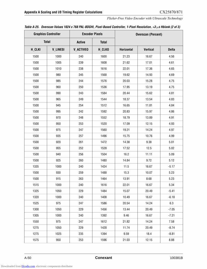
Appendix A Scaling and I/0 Timing Register Calculations CX25870/871
Flicker-Free Video Encoder with Ultrascale Technology
A-50 Conexant 100381B
1500 1000 240 1600 21.23 16.67 4.56
1500 1005 239 1608 21.62 17.01 4.61
1500 1010 238 1616 22.01 17.36 4.65
1500 980 245 1568 19.62 14.93 4.69
1500 985 244 1576 20.03 15.28 4.75
1500 960 250 1536 17.95 13.19 4.75
1500 990 243 1584 20.44 15.62 4.81
1500 965 249 1544 18.37 13.54 4.83
1500 945 254 1512 16.65 11.81 4.84
1500 995 242 1592 20.83 15.97 4.86
1500 970 248 1552 18.79 13.89 4.91
1500 950 253 1520 17.09 12.15 4.93
1500 975 247 1560 19.21 14.24 4.97
1500 935 257 1496 15.75 10.76 4.99
1500 920 261 1472 14.38 9.38 5.01
1500 955 252 1528 17.52 12.5 5.02
1500 940 256 1504 16.2 11.11 5.09
1500 925 260 1480 14.84 9.72 5.12
1335 1000 240 1424 11.5 16.67 -5.17
1500 930 259 1488 15.3 10.07 5.23
1500 915 263 1464 13.91 8.68 5.23
1515 1000 240 1616 22.01 16.67 5.34
1325 1050 229 1484 15.07 20.49 -5.41
1320 1000 240 1408 10.49 16.67 -6.18
1525 975 247 1586 20.54 14.24 6.3
1300 1050 229 1456 13.44 20.49 -7.05
1305 1000 240 1392 9.46 16.67 -7.21
1550 975 247 1612 21.82 14.24 7.58
1275 1050 229 1428 11.74 20.49 -8.74
1275 1025 235 1394 9.59 18.4 -8.81
1575 950 253 1596 21.03 12.15 8.88
Table A-25. Overscan Values 1024 x 768 PAL-BDGHI, Pixel-Based Controller, 1-Pixel Resolution, >3 !s Hblank (2 of 3)
Graphics Controller Encoder Pixels Overscan (Percent)
Total Active Total
H_CLKI V_LINESI V_ACTIVEO H_CLKO Horizontal Vertical Delta
Downloaded from Elcodis.com electronic components distributor
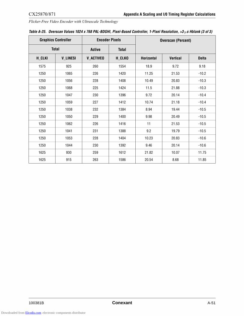
CX25870/871 Appendix A Scaling and I/0 Timing Register Calculations
Flicker-Free Video Encoder with Ultrascale Technology
100381B Conexant A-51
1575 925 260 1554 18.9 9.72 9.18
1250 1065 226 1420 11.25 21.53 -10.2
1250 1056 228 1408 10.49 20.83 -10.3
1250 1068 225 1424 11.5 21.88 -10.3
1250 1047 230 1396 9.72 20.14 -10.4
1250 1059 227 1412 10.74 21.18 -10.4
1250 1038 232 1384 8.94 19.44 -10.5
1250 1050 229 1400 9.98 20.49 -10.5
1250 1062 226 1416 11 21.53 -10.5
1250 1041 231 1388 9.2 19.79 -10.5
1250 1053 228 1404 10.23 20.83 -10.6
1250 1044 230 1392 9.46 20.14 -10.6
1625 930 259 1612 21.82 10.07 11.75
1625 915 263 1586 20.54 8.68 11.85
Table A-25. Overscan Values 1024 x 768 PAL-BDGHI, Pixel-Based Controller, 1-Pixel Resolution, >3 !s Hblank (3 of 3)
Graphics Controller Encoder Pixels Overscan (Percent)
Total Active Total
H_CLKI V_LINESI V_ACTIVEO H_CLKO Horizontal Vertical Delta
Downloaded from Elcodis.com electronic components distributor
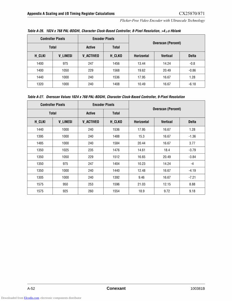
Appendix A Scaling and I/0 Timing Register Calculations CX25870/871
Flicker-Free Video Encoder with Ultrascale Technology
A-52 Conexant 100381B
Table A-26. 1024 x 768 PAL-BDGHI, Character Clock-Based Controller, 8-Pixel Resolution, >4 !s Hblank
Controller Pixels Encoder PixelsOverscan (Percent)
Total Active Total
H_CLKI V_LINESI V_ACTIVEO H_CLKO Horizontal Vertical Delta
1400 975 247 1456 13.44 14.24 -0.8
1400 1050 229 1568 19.62 20.49 -0.86
1440 1000 240 1536 17.95 16.67 1.28
1320 1000 240 1408 10.49 16.67 -6.18
Table A-27. Overscan Values 1024 x 768 PAL-BDGHI, Character Clock-Based Controller, 9-Pixel Resolution
Controller Pixels Encoder PixelsOverscan (Percent)
Total Active Total
H_CLKI V_LINESI V_ACTIVEO H_CLKO Horizontal Vertical Delta
1440 1000 240 1536 17.95 16.67 1.28
1395 1000 240 1488 15.3 16.67 -1.36
1485 1000 240 1584 20.44 16.67 3.77
1350 1025 235 1476 14.61 18.4 -3.79
1350 1050 229 1512 16.65 20.49 -3.84
1350 975 247 1404 10.23 14.24 -4
1350 1000 240 1440 12.48 16.67 -4.19
1305 1000 240 1392 9.46 16.67 -7.21
1575 950 253 1596 21.03 12.15 8.88
1575 925 260 1554 18.9 9.72 9.18
Downloaded from Elcodis.com electronic components distributor

100381B Conexant B-1
B
Appendix B Approved Crystal Vendors
Conexant conducted a series of internal tests and used the results to generate this
list of approved crystal vendors for the CX25870/871. Manufacturers not
appearing in this list may be acceptable, but verification testing on the target PCB
with samples is recommended.
Standard Crystal (El Monte, CA)
Phone Number: (626) 443-2121
FAX Number: (626) 443-9049
E-mail: [email protected]
Part Numbers for 13.500 MHz, Fundamental, 20 pF Load Crystal with an HC49U
Type of Package:
Full Height/50 ppm Total Tolerance: AAL13M500000GXE20A
Half-Height/50 ppm: AAK13M500000GXE20A
Full Height/25 ppm: Did Not Qualify
MMD Components (Irvine, CA)
Phone Number: (949) 753-5888
FAX Number: (949) 753-5889
E-mail: [email protected]
Internet: www.mmdcomp.com
Part Numbers for 13.500 MHz, Fundamental, 20 pF Load Crystal with an HC49U
Type of Package:
Full Height/50ppm Total Tolerance: A20BA1-13.500 MHz
Half-Height/50 ppm: B20BA1-13.500 MHz
Full Height/25 ppm: MMC-135-13.500 MHz (not tested)
Half Height/25 ppm: MMC-136-13.500 MHz (not tested)
General Electronics Devices (San Marcos, CA)
Phone Number: (760) 591-4170
FAX Number: (760) 591-4164
E-mail: [email protected]
Internet: www.gedlm.com
Part Numbers for 13.500 MHz, Fundamental, 20 pF Load Crystal with an HC49U
Type of Package:
Full Height/50 ppm Total Tolerance: PKHC49-13.500-.020-.005
Half-Height/50 ppm: PKHC49/-13.500-.020-.005
Full Height/25 ppm: PKHC49/-13.500-.020-.0025-15R
Half-Height/25 ppm: PKHC49/-13.500-.020-.0025
Downloaded from Elcodis.com electronic components distributor
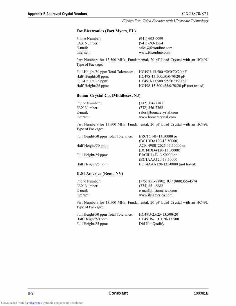
Appendix B Approved Crystal Vendors CX25870/871
Flicker-Free Video Encoder with Ultrascale Technology
B-2 Conexant 100381B
Fox Electronics (Fort Myers, FL)
Phone Number: (941) 693-0099
FAX Number: (941) 693-1554
E-mail: [email protected]
Internet: www.foxonline.com
Part Numbers for 13.500 MHz, Fundamental, 20 pF Load Crystal with an HC49U
Type of Package:
Full-Height/50 ppm Total Tolerance: HC49U-13.500 /50/0/70/20 pF
Half-Height/50 ppm: HC49S-13.500/50/0/70/20 pF
Full-Height/25 ppm: HC49U-13.500 /25/0/70/20 pF
Half-Height/25 ppm: HC49S-13.500 /25/0/70/20 pF (not tested)
Bomar Crystal Co. (Middlesex, NJ)
Phone Number: (732) 356-7787
FAX Number: (732) 356-7362
E-mail: [email protected]
Internet: www.bomarcrystal.com
Part Numbers for 13.500 MHz, Fundamental, 20 pF Load Crystal with an HC49U
Type of Package:
Full Height/50 ppm Total Tolerance: BRC1C14F-13.50000 or
(BC1DDA120-13.50000)
Half Height/50 ppm: ACR-49S012025-13.50000 or
(BC14DDA120-13.50000)
Full Height/25 ppm: BRCIH14F-13.50000 or
(BC1AAA120-13.50000
Half Height/25 ppm: BC14AAA120-13.50000 (not tested)
ILSI America (Reno, NV)
Phone Number: (775) 851-8880x103 / (888)355-4574
FAX Number: (775) 851-8882
E-mail: [email protected]
Internet: www.ilsiamerica.com
Part Numbers for 13.500 MHz, Fundamental, 20 pF Load Crystal with an HC49U
Type of Package:
Full Height/50 ppm Total Tolerance: HC49U-25/25-13.500-20
Half Height/50 ppm: HC49US-FB1F20-13.500
Full Height/25 ppm: Did Not Qualify
Downloaded from Elcodis.com electronic components distributor
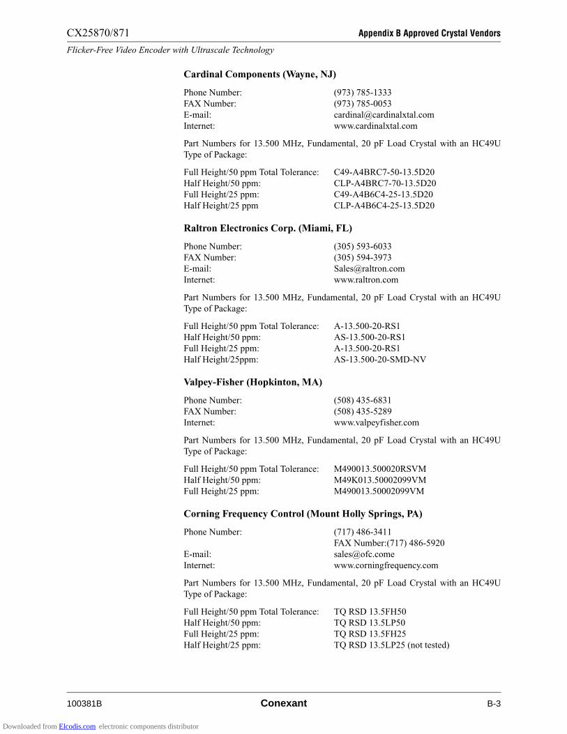
CX25870/871 Appendix B Approved Crystal Vendors
Flicker-Free Video Encoder with Ultrascale Technology
100381B Conexant B-3
Cardinal Components (Wayne, NJ)
Phone Number: (973) 785-1333
FAX Number: (973) 785-0053
E-mail: [email protected]
Internet: www.cardinalxtal.com
Part Numbers for 13.500 MHz, Fundamental, 20 pF Load Crystal with an HC49U
Type of Package:
Full Height/50 ppm Total Tolerance: C49-A4BRC7-50-13.5D20
Half Height/50 ppm: CLP-A4BRC7-70-13.5D20
Full Height/25 ppm: C49-A4B6C4-25-13.5D20
Half Height/25 ppm CLP-A4B6C4-25-13.5D20
Raltron Electronics Corp. (Miami, FL)
Phone Number: (305) 593-6033
FAX Number: (305) 594-3973
E-mail: [email protected]
Internet: www.raltron.com
Part Numbers for 13.500 MHz, Fundamental, 20 pF Load Crystal with an HC49U
Type of Package:
Full Height/50 ppm Total Tolerance: A-13.500-20-RS1
Half Height/50 ppm: AS-13.500-20-RS1
Full Height/25 ppm: A-13.500-20-RS1
Half Height/25ppm: AS-13.500-20-SMD-NV
Valpey-Fisher (Hopkinton, MA)
Phone Number: (508) 435-6831
FAX Number: (508) 435-5289
Internet: www.valpeyfisher.com
Part Numbers for 13.500 MHz, Fundamental, 20 pF Load Crystal with an HC49U
Type of Package:
Full Height/50 ppm Total Tolerance: M490013.500020RSVM
Half Height/50 ppm: M49K013.50002099VM
Full Height/25 ppm: M490013.50002099VM
Corning Frequency Control (Mount Holly Springs, PA)
Phone Number: (717) 486-3411
FAX Number:(717) 486-5920
E-mail: [email protected]
Internet: www.corningfrequency.com
Part Numbers for 13.500 MHz, Fundamental, 20 pF Load Crystal with an HC49U
Type of Package:
Full Height/50 ppm Total Tolerance: TQ RSD 13.5FH50
Half Height/50 ppm: TQ RSD 13.5LP50
Full Height/25 ppm: TQ RSD 13.5FH25
Half Height/25 ppm: TQ RSD 13.5LP25 (not tested)
Downloaded from Elcodis.com electronic components distributor
Appendix B Approved Crystal Vendors CX25870/871
Flicker-Free Video Encoder with Ultrascale Technology
B-4 Conexant 100381B
Downloaded from Elcodis.com electronic components distributor
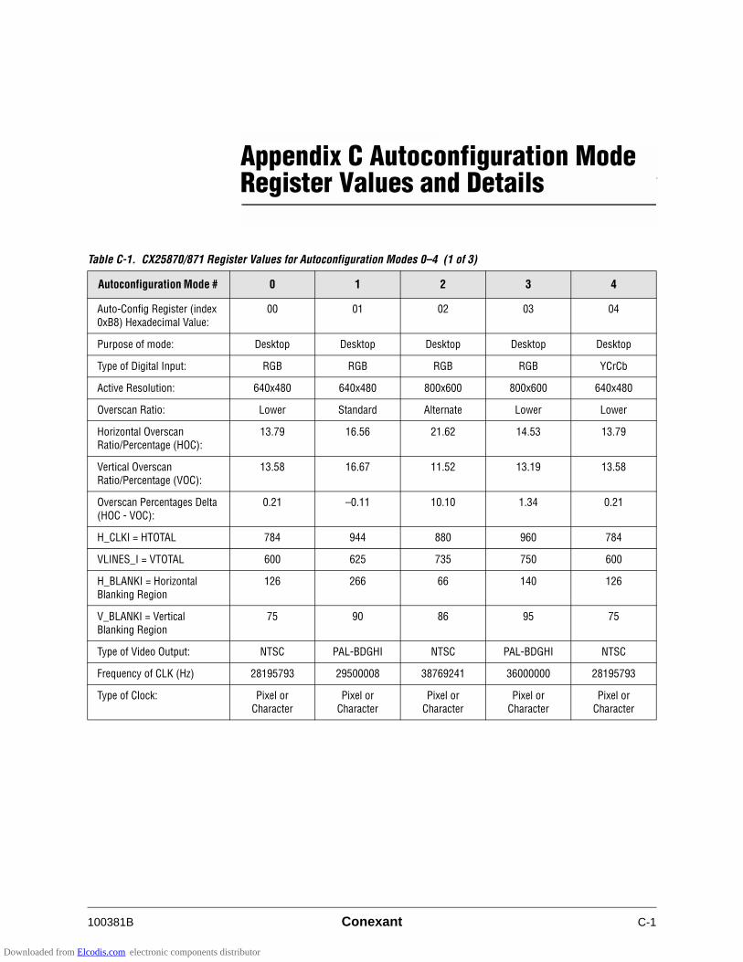
100381B Conexant C-1
C
Appendix C Autoconfiguration Mode Register Values and Details
Table C-1. CX25870/871 Register Values for Autoconfiguration Modes 0–4 (1 of 3)
Autoconfiguration Mode # 0 1 2 3 4
Auto-Config Register (index
0xB8) Hexadecimal Value:
00 01 02 03 04
Purpose of mode: Desktop Desktop Desktop Desktop Desktop
Type of Digital Input: RGB RGB RGB RGB YCrCb
Active Resolution: 640x480 640x480 800x600 800x600 640x480
Overscan Ratio: Lower Standard Alternate Lower Lower
Horizontal Overscan Ratio/Percentage (HOC):
13.79 16.56 21.62 14.53 13.79
Vertical Overscan Ratio/Percentage (VOC):
13.58 16.67 11.52 13.19 13.58
Overscan Percentages Delta (HOC - VOC):
0.21 –0.11 10.10 1.34 0.21
H_CLKI = HTOTAL 784 944 880 960 784
VLINES_I = VTOTAL 600 625 735 750 600
H_BLANKI = Horizontal Blanking Region
126 266 66 140 126
V_BLANKI = Vertical
Blanking Region
75 90 86 95 75
Type of Video Output: NTSC PAL-BDGHI NTSC PAL-BDGHI NTSC
Frequency of CLK (Hz) 28195793 29500008 38769241 36000000 28195793
Type of Clock: Pixel or Character
Pixel or Character
Pixel or Character
Pixel or Character
Pixel or Character
Downloaded from Elcodis.com electronic components distributor

Appendix C Autoconfiguration Mode Register Values and Details CX25870/871
Flicker-Free Video Encoder with Ultrascale Technology
C-2 Conexant 100381B
Register AddressRegister
ValueRegister
ValueRegister
ValueRegister
ValueRegister
Value
0x38 00 00 00 00 00
0x76 00 60 A0 00 00
0x78 80 80 20 20 80
0x7A 84 8A B6 AA 84
0x7C 96 A6 CE CA 96
0x7E 60 68 B4 9A 60
0x80 7D C1 55 0D 7D
0x82 22 2E 20 29 22
0x84 D4 F2 D8 FC D4
0x86 27 27 39 39 27
0x88 00 00 00 00 00
0x8A 10 B0 70 C0 10
0x8C 7E 0A 42 8C 7E
0x8E 03 0B 03 03 03
0x90 58 71 DF EE 58
0x92 4B 5A 56 5F 4B
0x94 E0 E0 58 58 E0
0x96 36 36 3A 3A 36
0x98 92 00 CD 66 92
0x9A 54 50 9C 96 54
0x9C 0E 72 14 00 0E
0x9E 88 1C 3B 00 88
0xA0 0C 0D 11 10 0C
0xA2 0A 24 0A 24 0A
0xA4 E5 F0 E5 F0 E5
0xA6 76 58 74 57 76
0xA8 79 81 77 80 79
0xAA 44 49 43 48 44
0xAC 85 8C 85 8C 85
0xAE 00 0C BA 18 00
Table C-1. CX25870/871 Register Values for Autoconfiguration Modes 0–4 (2 of 3)
Autoconfiguration Mode # 0 1 2 3 4
Downloaded from Elcodis.com electronic components distributor
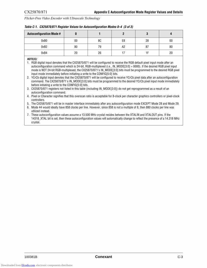
CX25870/871 Appendix C Autoconfiguration Mode Register Values and Details
Flicker-Free Video Encoder with Ultrascale Technology
100381B Conexant C-3
0xB0 00 8C E8 28 00
0xB2 80 79 A2 87 80
0xB4 20 26 17 1F 20
NOTE(S):
1. RGB digital input denotes that the CX25870/871 will be configured to receive the RGB default pixel input mode after an autoconfiguration command which is 24-bit, RGB-multiplexed (i.e., IN_MODE[3:0] = 0000). If the desired RGB pixel input
mode is NOT 24-bit RGB-multiplexed, the CX25870/871's IN_MODE[3:0] bits must be programmed to the desired RGB pixel input mode immediately before initiating a write to the CONFIG[5:0] bits.
2. YCrCb digital input denotes that the CX25870/871 will be configured to receive YCrCb pixel data after an autoconfiguration
command. The CX25870/871's IN_MODE[3:0] bits must be programmed to the desired YCrCb pixel input mode immediately before initiating a write to the CONFIG[5:0] bits.
3. CX25870/871 registers not listed in this table (including IN_MODE[3:0]) do not get reprogrammed as a result of an
autoconfiguration command.4. Pixel or Character signifies that this overscan ratio is acceptable for 8-clock per character graphics controllers or pixel-clock
controllers.
5. The CX25870/871 will be in master interface immediately after any autoconfiguration mode EXCEPT Mode 28 and Mode 29.6. Mode 44 would ideally have 858 clocks per line. However, since 858 is not a multiple of 8, then 880 clocks per line was
utilized instead.
7. These autoconfiguration values assume a 13.500 MHz crystal resides between the XTALIN and XTALOUT pins. If the 14318_XTAL bit is set, then these autoconfiguration values will automatically change to reflect the presence of a 14.318 MHz crystal.
Table C-1. CX25870/871 Register Values for Autoconfiguration Modes 0–4 (3 of 3)
Autoconfiguration Mode # 0 1 2 3 4
Downloaded from Elcodis.com electronic components distributor
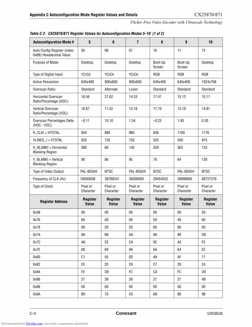
Appendix C Autoconfiguration Mode Register Values and Details CX25870/871
Flicker-Free Video Encoder with Ultrascale Technology
C-4 Conexant 100381B
Table C-2. CX25870/871 Register Values for Autoconfiguration Modes 5–10 (1 of 2)
Autoconfiguration Mode # 5 6 7 8 9 10
Auto-Config Register (index 0xB8) Hexadecimal Value:
05 06 07 10 11 12
Purpose of Mode: Desktop Desktop Desktop Boot-Up
Screen
Boot-Up
Screen
Desktop
Type of Digital Input: YCrCb YCrCb YCrCb RGB RGB RGB
Active Resolution: 640x480 800x600 800x600 640x400 640x400 1024x768
Overscan Ratio: Standard Alternate Lower Standard Standard Standard
Horizontal Overscan Ratio/Percentage (HOC):
16.56 21.62 14.53 17.47 15.12 15.11
Vertical Overscan Ratio/Percentage (VOC):
16.67 11.52 13.19 17.70 13.19 14.81
Overscan Percentages Delta
(HOC - VOC):
–0.11 10.10 1.34 –0.23 1.93 0.30
H_CLKI = HTOTAL 944 880 960 936 1160 1176
VLINES_I = VTOTAL 625 735 750 525 500 975
H_BLANKI = Horizontal Blanking Region
266 66 140 259 363 133
V_BLANKI = Vertical Blanking Region
90 86 95 76 64 130
Type of Video Output: PAL-BDGHI NTSC PAL-BDGHI NTSC PAL-BDGHI NTSC
Frequency of CLK (Hz) 29500008 38769241 36000000 29454552 28999992 68727276
Type of Clock: Pixel or
Character
Pixel or
Character
Pixel or
Character
Pixel or
Character
Pixel or
Character
Pixel or
Character
Register AddressRegister
ValueRegister
ValueRegister
ValueRegister
ValueRegister
ValueRegister
Value
0x38 00 00 00 00 00 20
0x76 60 A0 00 50 40 60
0x78 80 20 20 80 80 00
0x7A 8A B6 AA 8A 88 D8
0x7C A6 CE CA 9C A2 F2
0x7E 68 B4 9A 6A 64 EE
0x80 C1 55 0D A9 AF 71
0x82 2E 20 29 27 29 24
0x84 F2 D8 FC CA FC D0
0x86 27 39 39 27 27 4B
0x88 00 00 00 00 00 00
0x8A B0 70 C0 A8 88 98
Downloaded from Elcodis.com electronic components distributor
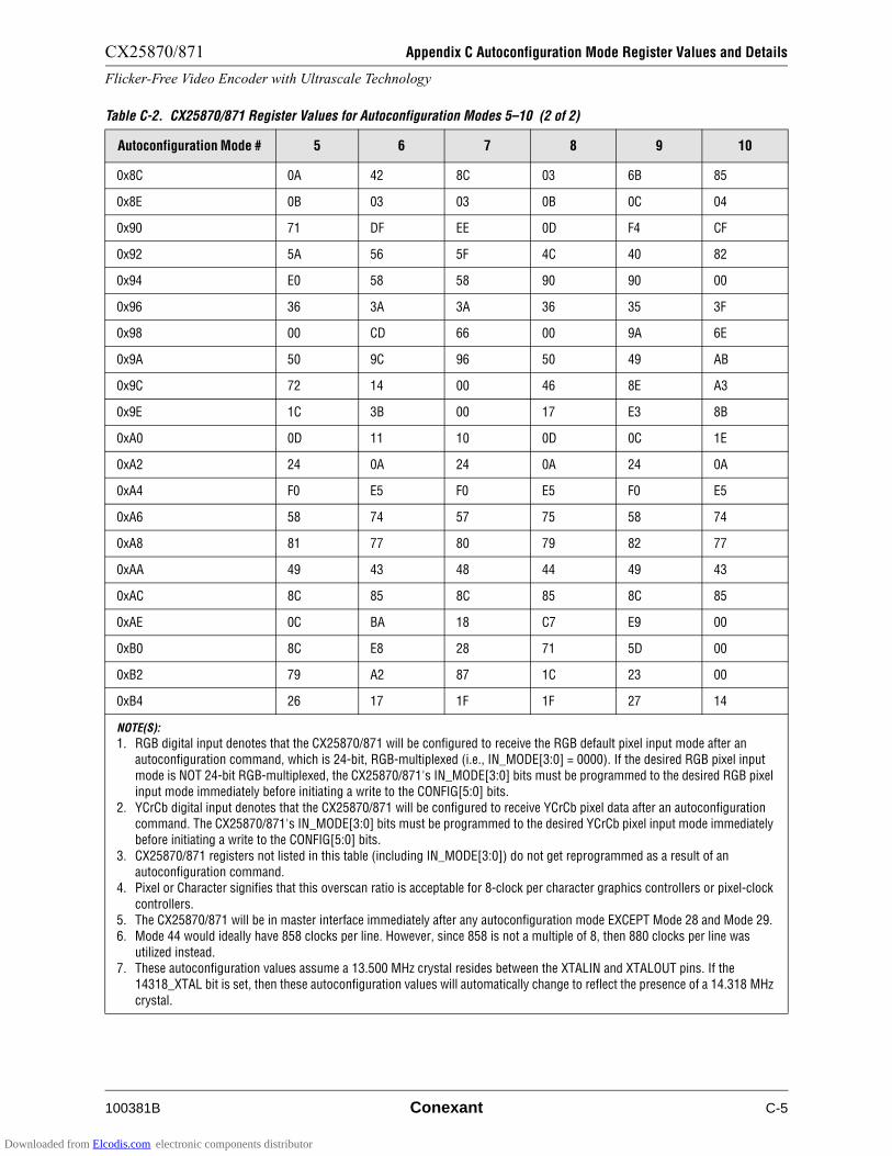
CX25870/871 Appendix C Autoconfiguration Mode Register Values and Details
Flicker-Free Video Encoder with Ultrascale Technology
100381B Conexant C-5
0x8C 0A 42 8C 03 6B 85
0x8E 0B 03 03 0B 0C 04
0x90 71 DF EE 0D F4 CF
0x92 5A 56 5F 4C 40 82
0x94 E0 58 58 90 90 00
0x96 36 3A 3A 36 35 3F
0x98 00 CD 66 00 9A 6E
0x9A 50 9C 96 50 49 AB
0x9C 72 14 00 46 8E A3
0x9E 1C 3B 00 17 E3 8B
0xA0 0D 11 10 0D 0C 1E
0xA2 24 0A 24 0A 24 0A
0xA4 F0 E5 F0 E5 F0 E5
0xA6 58 74 57 75 58 74
0xA8 81 77 80 79 82 77
0xAA 49 43 48 44 49 43
0xAC 8C 85 8C 85 8C 85
0xAE 0C BA 18 C7 E9 00
0xB0 8C E8 28 71 5D 00
0xB2 79 A2 87 1C 23 00
0xB4 26 17 1F 1F 27 14
NOTE(S):
1. RGB digital input denotes that the CX25870/871 will be configured to receive the RGB default pixel input mode after an autoconfiguration command, which is 24-bit, RGB-multiplexed (i.e., IN_MODE[3:0] = 0000). If the desired RGB pixel input
mode is NOT 24-bit RGB-multiplexed, the CX25870/871's IN_MODE[3:0] bits must be programmed to the desired RGB pixel input mode immediately before initiating a write to the CONFIG[5:0] bits.
2. YCrCb digital input denotes that the CX25870/871 will be configured to receive YCrCb pixel data after an autoconfiguration command. The CX25870/871's IN_MODE[3:0] bits must be programmed to the desired YCrCb pixel input mode immediately before initiating a write to the CONFIG[5:0] bits.
3. CX25870/871 registers not listed in this table (including IN_MODE[3:0]) do not get reprogrammed as a result of an autoconfiguration command.
4. Pixel or Character signifies that this overscan ratio is acceptable for 8-clock per character graphics controllers or pixel-clock
controllers.5. The CX25870/871 will be in master interface immediately after any autoconfiguration mode EXCEPT Mode 28 and Mode 29.6. Mode 44 would ideally have 858 clocks per line. However, since 858 is not a multiple of 8, then 880 clocks per line was
utilized instead.7. These autoconfiguration values assume a 13.500 MHz crystal resides between the XTALIN and XTALOUT pins. If the
14318_XTAL bit is set, then these autoconfiguration values will automatically change to reflect the presence of a 14.318 MHz
crystal.
Table C-2. CX25870/871 Register Values for Autoconfiguration Modes 5–10 (2 of 2)
Autoconfiguration Mode # 5 6 7 8 9 10
Downloaded from Elcodis.com electronic components distributor
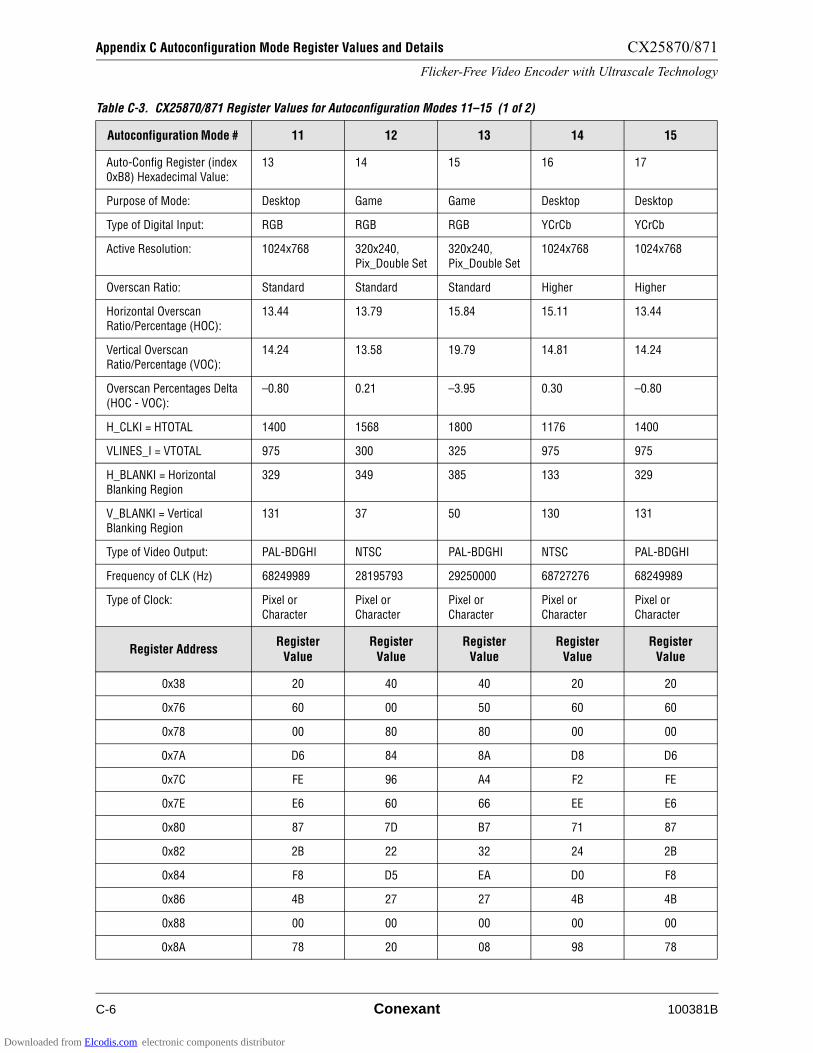
Appendix C Autoconfiguration Mode Register Values and Details CX25870/871
Flicker-Free Video Encoder with Ultrascale Technology
C-6 Conexant 100381B
Table C-3. CX25870/871 Register Values for Autoconfiguration Modes 11–15 (1 of 2)
Autoconfiguration Mode # 11 12 13 14 15
Auto-Config Register (index 0xB8) Hexadecimal Value:
13 14 15 16 17
Purpose of Mode: Desktop Game Game Desktop Desktop
Type of Digital Input: RGB RGB RGB YCrCb YCrCb
Active Resolution: 1024x768 320x240,
Pix_Double Set
320x240,
Pix_Double Set
1024x768 1024x768
Overscan Ratio: Standard Standard Standard Higher Higher
Horizontal Overscan Ratio/Percentage (HOC):
13.44 13.79 15.84 15.11 13.44
Vertical Overscan Ratio/Percentage (VOC):
14.24 13.58 19.79 14.81 14.24
Overscan Percentages Delta
(HOC - VOC):
–0.80 0.21 –3.95 0.30 –0.80
H_CLKI = HTOTAL 1400 1568 1800 1176 1400
VLINES_I = VTOTAL 975 300 325 975 975
H_BLANKI = Horizontal Blanking Region
329 349 385 133 329
V_BLANKI = Vertical Blanking Region
131 37 50 130 131
Type of Video Output: PAL-BDGHI NTSC PAL-BDGHI NTSC PAL-BDGHI
Frequency of CLK (Hz) 68249989 28195793 29250000 68727276 68249989
Type of Clock: Pixel or
Character
Pixel or
Character
Pixel or
Character
Pixel or
Character
Pixel or
Character
Register AddressRegister
ValueRegister
ValueRegister
ValueRegister
ValueRegister
Value
0x38 20 40 40 20 20
0x76 60 00 50 60 60
0x78 00 80 80 00 00
0x7A D6 84 8A D8 D6
0x7C FE 96 A4 F2 FE
0x7E E6 60 66 EE E6
0x80 87 7D B7 71 87
0x82 2B 22 32 24 2B
0x84 F8 D5 EA D0 F8
0x86 4B 27 27 4B 4B
0x88 00 00 00 00 00
0x8A 78 20 08 98 78
Downloaded from Elcodis.com electronic components distributor
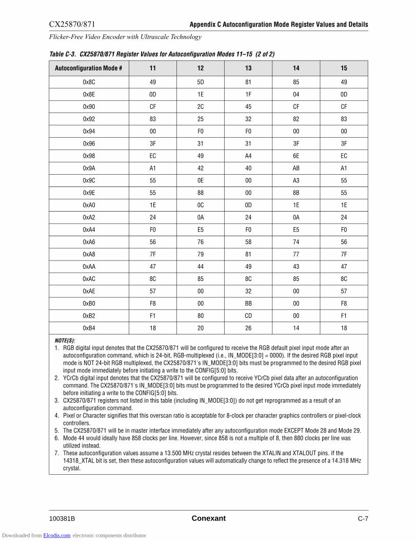
CX25870/871 Appendix C Autoconfiguration Mode Register Values and Details
Flicker-Free Video Encoder with Ultrascale Technology
100381B Conexant C-7
0x8C 49 5D 81 85 49
0x8E 0D 1E 1F 04 0D
0x90 CF 2C 45 CF CF
0x92 83 25 32 82 83
0x94 00 F0 F0 00 00
0x96 3F 31 31 3F 3F
0x98 EC 49 A4 6E EC
0x9A A1 42 40 AB A1
0x9C 55 0E 00 A3 55
0x9E 55 88 00 8B 55
0xA0 1E 0C 0D 1E 1E
0xA2 24 0A 24 0A 24
0xA4 F0 E5 F0 E5 F0
0xA6 56 76 58 74 56
0xA8 7F 79 81 77 7F
0xAA 47 44 49 43 47
0xAC 8C 85 8C 85 8C
0xAE 57 00 32 00 57
0xB0 F8 00 BB 00 F8
0xB2 F1 80 CD 00 F1
0xB4 18 20 26 14 18
NOTE(S):
1. RGB digital input denotes that the CX25870/871 will be configured to receive the RGB default pixel input mode after an autoconfiguration command, which is 24-bit, RGB-multiplexed (i.e., IN_MODE[3:0] = 0000). If the desired RGB pixel input
mode is NOT 24-bit RGB multiplexed, the CX25870/871's IN_MODE[3:0] bits must be programmed to the desired RGB pixel input mode immediately before initiating a write to the CONFIG[5:0] bits.
2. YCrCb digital input denotes that the CX25870/871 will be configured to receive YCrCb pixel data after an autoconfiguration command. The CX25870/871's IN_MODE[3:0] bits must be programmed to the desired YCrCb pixel input mode immediately before initiating a write to the CONFIG[5:0] bits.
3. CX25870/871 registers not listed in this table (including IN_MODE[3:0]) do not get reprogrammed as a result of an autoconfiguration command.
4. Pixel or Character signifies that this overscan ratio is acceptable for 8-clock per character graphics controllers or pixel-clock
controllers.5. The CX25870/871 will be in master interface immediately after any autoconfiguration mode EXCEPT Mode 28 and Mode 29.6. Mode 44 would ideally have 858 clocks per line. However, since 858 is not a multiple of 8, then 880 clocks per line was
utilized instead.7. These autoconfiguration values assume a 13.500 MHz crystal resides between the XTALIN and XTALOUT pins. If the
14318_XTAL bit is set, then these autoconfiguration values will automatically change to reflect the presence of a 14.318 MHz
crystal.
Table C-3. CX25870/871 Register Values for Autoconfiguration Modes 11–15 (2 of 2)
Autoconfiguration Mode # 11 12 13 14 15
Downloaded from Elcodis.com electronic components distributor
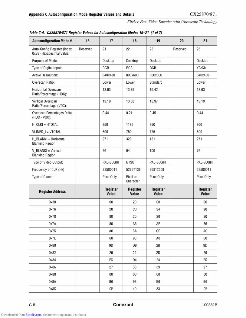
Appendix C Autoconfiguration Mode Register Values and Details CX25870/871
Flicker-Free Video Encoder with Ultrascale Technology
C-8 Conexant 100381B
Table C-4. CX25870/871 Register Values for Autoconfiguration Modes 16–21 (1 of 2)
Autoconfiguration Mode # 16 17 18 19 20 21
Auto-Config Register (index 0xB8) Hexadecimal Value:
Reserved 21 22 23 Reserved 25
Purpose of Mode: Desktop Desktop Desktop Desktop
Type of Digital Input: RGB RGB RGB YCrCb
Active Resolution: 640x480 800x600 800x600 640x480
Overscan Ratio: Lower Lower Standard Lower
Horizontal Overscan
Ratio/Percentage (HOC):
13.63 13.79 16.42 13.63
Vertical Overscan Ratio/Percentage (VOC):
13.19 13.58 15.97 13.19
Overscan Percentages Delta (HOC - VOC):
0.44 0.21 0.45 0.44
H_CLKI = HTOTAL 950 1176 950 950
VLINES_I = VTOTAL 600 750 775 600
H_BLANKI = Horizontal
Blanking Region
271 329 131 271
V_BLANKI = Vertical Blanking Region
76 94 109 76
Type of Video Output: PAL-BDGHI NTSC PAL-BDGHI PAL-BDGHI
Frequency of CLK (Hz) 28500011 52867138 36812508 28500011
Type of Clock: Pixel Only Pixel or Character
Pixel Only Pixel Only
Register AddressRegister
ValueRegister
ValueRegister
ValueRegister
Value
0x38 00 20 00 00
0x76 20 C0 34 20
0x78 80 20 20 80
0x7A 86 A6 AE 86
0x7C A0 BA CE A0
0x7E 60 98 A0 60
0x80 9D D9 2B 9D
0x82 29 22 2D 29
0x84 FC D4 F4 FC
0x86 27 38 39 27
0x88 00 00 00 00
0x8A B6 98 B6 B6
0x8C 0F 49 83 0F
Downloaded from Elcodis.com electronic components distributor
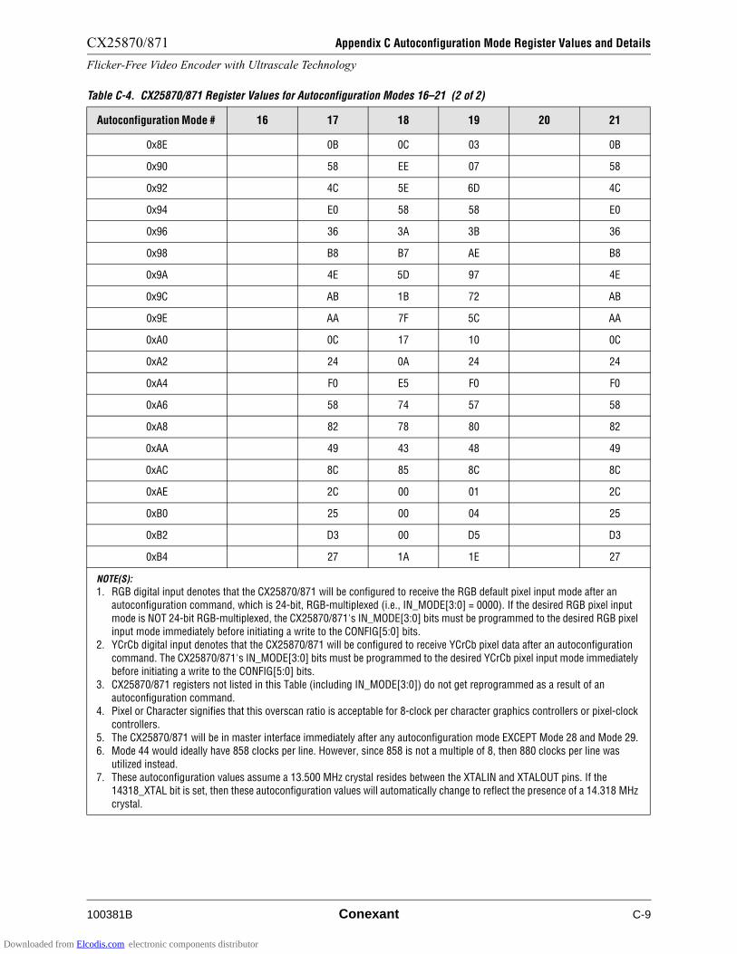
CX25870/871 Appendix C Autoconfiguration Mode Register Values and Details
Flicker-Free Video Encoder with Ultrascale Technology
100381B Conexant C-9
0x8E 0B 0C 03 0B
0x90 58 EE 07 58
0x92 4C 5E 6D 4C
0x94 E0 58 58 E0
0x96 36 3A 3B 36
0x98 B8 B7 AE B8
0x9A 4E 5D 97 4E
0x9C AB 1B 72 AB
0x9E AA 7F 5C AA
0xA0 0C 17 10 0C
0xA2 24 0A 24 24
0xA4 F0 E5 F0 F0
0xA6 58 74 57 58
0xA8 82 78 80 82
0xAA 49 43 48 49
0xAC 8C 85 8C 8C
0xAE 2C 00 01 2C
0xB0 25 00 04 25
0xB2 D3 00 D5 D3
0xB4 27 1A 1E 27
NOTE(S):
1. RGB digital input denotes that the CX25870/871 will be configured to receive the RGB default pixel input mode after an autoconfiguration command, which is 24-bit, RGB-multiplexed (i.e., IN_MODE[3:0] = 0000). If the desired RGB pixel input
mode is NOT 24-bit RGB-multiplexed, the CX25870/871's IN_MODE[3:0] bits must be programmed to the desired RGB pixel input mode immediately before initiating a write to the CONFIG[5:0] bits.
2. YCrCb digital input denotes that the CX25870/871 will be configured to receive YCrCb pixel data after an autoconfiguration
command. The CX25870/871's IN_MODE[3:0] bits must be programmed to the desired YCrCb pixel input mode immediately before initiating a write to the CONFIG[5:0] bits.
3. CX25870/871 registers not listed in this Table (including IN_MODE[3:0]) do not get reprogrammed as a result of an autoconfiguration command.
4. Pixel or Character signifies that this overscan ratio is acceptable for 8-clock per character graphics controllers or pixel-clock
controllers.5. The CX25870/871 will be in master interface immediately after any autoconfiguration mode EXCEPT Mode 28 and Mode 29.6. Mode 44 would ideally have 858 clocks per line. However, since 858 is not a multiple of 8, then 880 clocks per line was
utilized instead.7. These autoconfiguration values assume a 13.500 MHz crystal resides between the XTALIN and XTALOUT pins. If the
14318_XTAL bit is set, then these autoconfiguration values will automatically change to reflect the presence of a 14.318 MHz
crystal.
Table C-4. CX25870/871 Register Values for Autoconfiguration Modes 16–21 (2 of 2)
Autoconfiguration Mode # 16 17 18 19 20 21
Downloaded from Elcodis.com electronic components distributor

Appendix C Autoconfiguration Mode Register Values and Details CX25870/871
Flicker-Free Video Encoder with Ultrascale Technology
C-10 Conexant 100381B
Table C-5. CX25870/871 Register Values for Autoconfiguration Modes 22–26 (1 of 2)
Autoconfiguration Mode # 22 23 24 25 26
Auto-Config Register (index 0xB8) Hexadecimal Value:
26 27 30 31 32
Purpose of Mode: Desktop Desktop Boot-Up Screen
Boot-Up Screen
Desktop
Type of Digital Input: YCrCb YCrCb RGB RGB RGB
Active Resolution: 800x600 800x600 720x400 720x400 1024x768
Overscan Ratio: Lower Standard Standard Standard Lower
Horizontal Overscan
Ratio/Percentage (HOC):
13.79 16.42 17.47 15.12 11.97
Vertical Overscan Ratio/Percentage (VOC):
13.58 15.97 17.70 13.19 11.93
Overscan Percentages Delta (HOC - VOC):
0.21 0.45 –0.23 1.93 0.04
H_CLKI = HTOTAL 1176 950 1053 1305 1170
VLINES_I = VTOTAL 750 775 525 500 945
H_BLANKI = Horizontal
Blanking Region
329 131 291 411 127
V_BLANKI = Vertical Blanking Region
94 109 76 64 115
Type of Video Output: NTSC PAL-BDGHI NTSC PAL-BDGHI NTSC
Frequency of CLK (Hz) 52867138 36812508 33136345 32625000 66272724
Type of Clock: Pixel or Character
Pixel Only Pixel or 9-Character
only
Pixel or 9-Character
only
Pixel Only
Register AddressRegister
ValueRegister
ValueRegister
ValueRegister
ValueRegister
Value
0x38 20 00 00 00 20
0x76 C0 34 3A 28 F8
0x78 20 20 D0 D0 00
0x7A A6 AE 9C 9A D0
0x7C BA CE B0 B6 EA
0x7E 98 A0 88 80 E0
0x80 D9 2B DD E3 37
0x82 22 2D 27 29 21
0x84 D4 F4 CA FC D7
0x86 38 39 28 28 4A
0x88 00 00 00 00 00
Downloaded from Elcodis.com electronic components distributor

CX25870/871 Appendix C Autoconfiguration Mode Register Values and Details
Flicker-Free Video Encoder with Ultrascale Technology
100381B Conexant C-11
0x8A 98 B6 1D 19 92
0x8C 49 83 23 9B 7F
0x8E 0C 03 0C 0D 04
0x90 EE 07 0D F4 B1
0x92 5E 6D 4C 40 73
0x94 58 58 90 90 00
0x96 3A 3B 36 35 3F
0x98 B7 AE 00 9A 9A
0x9A 5D 97 50 49 A9
0x9C 1B 72 2E 00 5D
0x9E 7F 5C BA 80 74
0xA0 17 10 0E 0E 1D
0xA2 0A 24 0A 24 0A
0xA4 E5 F0 E5 F0 E5
0xA6 74 57 75 57 74
0xA8 78 80 78 80 77
0xAA 43 48 43 48 43
0xAC 85 8C 85 8C 85
0xAE 00 01 95 97 2F
0xB0 00 04 81 1A A1
0xB2 00 D5 A7 CA BD
0xB4 1A 1E 1B 22 14
NOTE(S):
1. RGB digital input denotes that the CX25870/871 will be configured to receive the RGB default pixel input mode after an autoconfiguration command, which is 24-bit, RGB-multiplexed (i.e., IN_MODE[3:0] = 0000). If the desired RGB pixel input
mode is NOT 24-bit RGB multiplexed, the CX25870/871's IN_MODE[3:0] bits must be programmed to the desired RGB pixel input mode immediately before initiating a write to the CONFIG[5:0] bits.
2. YCrCb digital input denotes that the CX25870/871 will be configured to receive YCrCb pixel data after an autoconfiguration command. The CX25870/871's IN_MODE[3:0] bits must be programmed to the desired YCrCb pixel input mode immediately before initiating a write to the CONFIG[5:0] bits.
3. CX25870/871 registers not listed in this table (including IN_MODE[3:0]) do not get reprogrammed as a result of an autoconfiguration command.
4. Pixel or Character signifies that this overscan ratio is acceptable for 8-clock per character graphics controllers or pixel-clock
controllers.5. The CX25870/871 will be in master interface immediately after any autoconfiguration mode EXCEPT Mode 28 and Mode 29.6. Mode 44 would ideally have 858 clocks per line. However, since 858 is not a multiple of 8, then 880 clocks per line was
utilized instead.7. These autoconfiguration values assume a 13.500 MHz crystal resides between the XTALIN and XTALOUT pins. If the
14318_XTAL bit is set, then these autoconfiguration values will automatically change to reflect the presence of a 14.318 MHz
crystal.
Table C-5. CX25870/871 Register Values for Autoconfiguration Modes 22–26 (2 of 2)
Autoconfiguration Mode # 22 23 24 25 26
Downloaded from Elcodis.com electronic components distributor
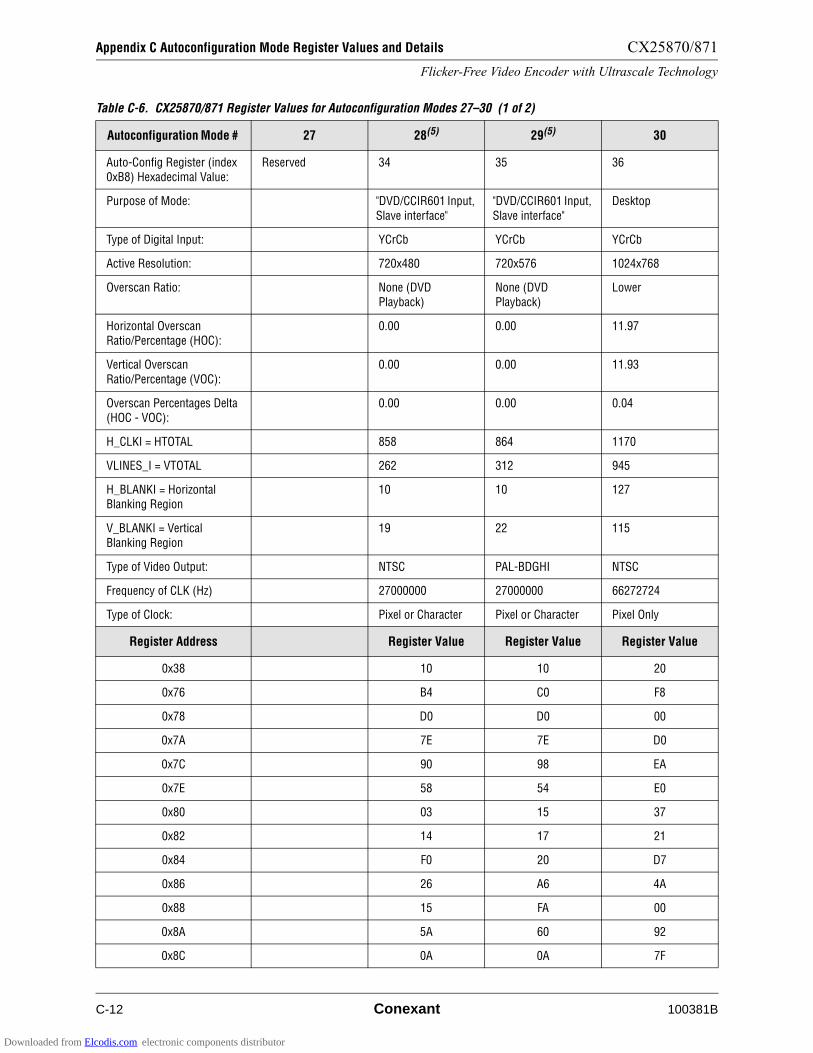
Appendix C Autoconfiguration Mode Register Values and Details CX25870/871
Flicker-Free Video Encoder with Ultrascale Technology
C-12 Conexant 100381B
Table C-6. CX25870/871 Register Values for Autoconfiguration Modes 27–30 (1 of 2)
Autoconfiguration Mode # 27 28(5) 29(5) 30
Auto-Config Register (index 0xB8) Hexadecimal Value:
Reserved 34 35 36
Purpose of Mode: "DVD/CCIR601 Input,
Slave interface"
"DVD/CCIR601 Input,
Slave interface"
Desktop
Type of Digital Input: YCrCb YCrCb YCrCb
Active Resolution: 720x480 720x576 1024x768
Overscan Ratio: None (DVD Playback)
None (DVD Playback)
Lower
Horizontal Overscan Ratio/Percentage (HOC):
0.00 0.00 11.97
Vertical Overscan
Ratio/Percentage (VOC):
0.00 0.00 11.93
Overscan Percentages Delta (HOC - VOC):
0.00 0.00 0.04
H_CLKI = HTOTAL 858 864 1170
VLINES_I = VTOTAL 262 312 945
H_BLANKI = Horizontal Blanking Region
10 10 127
V_BLANKI = Vertical
Blanking Region
19 22 115
Type of Video Output: NTSC PAL-BDGHI NTSC
Frequency of CLK (Hz) 27000000 27000000 66272724
Type of Clock: Pixel or Character Pixel or Character Pixel Only
Register Address Register Value Register Value Register Value
0x38 10 10 20
0x76 B4 C0 F8
0x78 D0 D0 00
0x7A 7E 7E D0
0x7C 90 98 EA
0x7E 58 54 E0
0x80 03 15 37
0x82 14 17 21
0x84 F0 20 D7
0x86 26 A6 4A
0x88 15 FA 00
0x8A 5A 60 92
0x8C 0A 0A 7F
Downloaded from Elcodis.com electronic components distributor
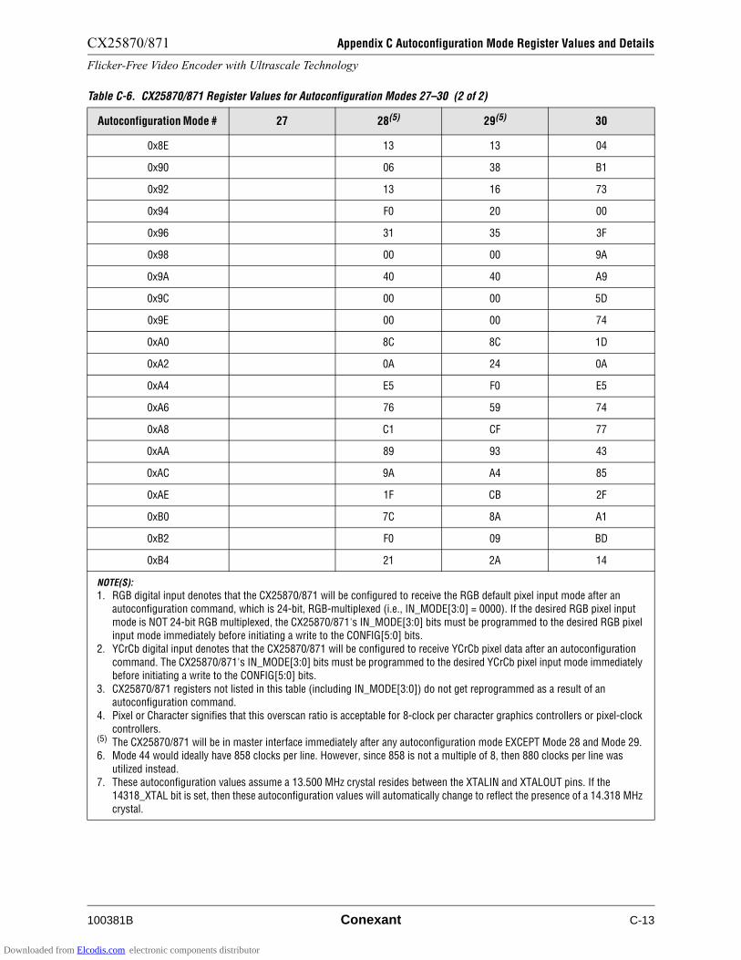
CX25870/871 Appendix C Autoconfiguration Mode Register Values and Details
Flicker-Free Video Encoder with Ultrascale Technology
100381B Conexant C-13
0x8E 13 13 04
0x90 06 38 B1
0x92 13 16 73
0x94 F0 20 00
0x96 31 35 3F
0x98 00 00 9A
0x9A 40 40 A9
0x9C 00 00 5D
0x9E 00 00 74
0xA0 8C 8C 1D
0xA2 0A 24 0A
0xA4 E5 F0 E5
0xA6 76 59 74
0xA8 C1 CF 77
0xAA 89 93 43
0xAC 9A A4 85
0xAE 1F CB 2F
0xB0 7C 8A A1
0xB2 F0 09 BD
0xB4 21 2A 14
NOTE(S):
1. RGB digital input denotes that the CX25870/871 will be configured to receive the RGB default pixel input mode after an autoconfiguration command, which is 24-bit, RGB-multiplexed (i.e., IN_MODE[3:0] = 0000). If the desired RGB pixel input
mode is NOT 24-bit RGB multiplexed, the CX25870/871's IN_MODE[3:0] bits must be programmed to the desired RGB pixel input mode immediately before initiating a write to the CONFIG[5:0] bits.
2. YCrCb digital input denotes that the CX25870/871 will be configured to receive YCrCb pixel data after an autoconfiguration
command. The CX25870/871's IN_MODE[3:0] bits must be programmed to the desired YCrCb pixel input mode immediately before initiating a write to the CONFIG[5:0] bits.
3. CX25870/871 registers not listed in this table (including IN_MODE[3:0]) do not get reprogrammed as a result of an autoconfiguration command.
4. Pixel or Character signifies that this overscan ratio is acceptable for 8-clock per character graphics controllers or pixel-clock
controllers.(5) The CX25870/871 will be in master interface immediately after any autoconfiguration mode EXCEPT Mode 28 and Mode 29.6. Mode 44 would ideally have 858 clocks per line. However, since 858 is not a multiple of 8, then 880 clocks per line was
utilized instead.7. These autoconfiguration values assume a 13.500 MHz crystal resides between the XTALIN and XTALOUT pins. If the
14318_XTAL bit is set, then these autoconfiguration values will automatically change to reflect the presence of a 14.318 MHz
crystal.
Table C-6. CX25870/871 Register Values for Autoconfiguration Modes 27–30 (2 of 2)
Autoconfiguration Mode # 27 28(5) 29(5) 30
Downloaded from Elcodis.com electronic components distributor
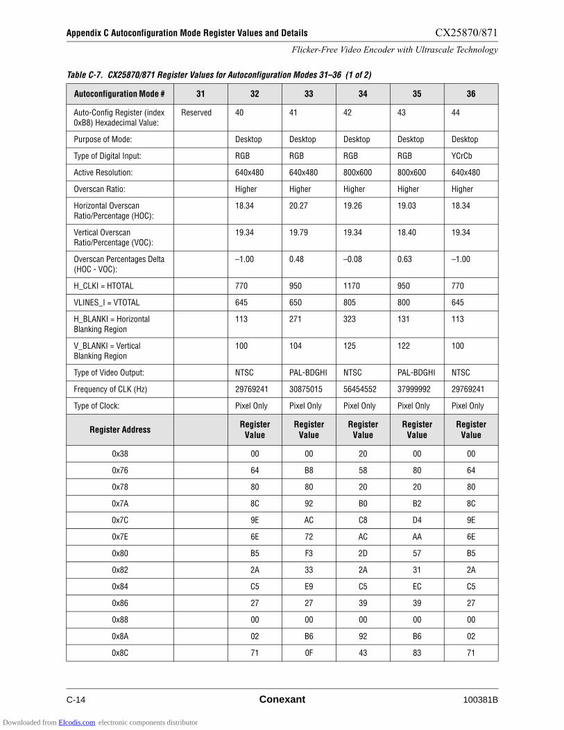
Appendix C Autoconfiguration Mode Register Values and Details CX25870/871
Flicker-Free Video Encoder with Ultrascale Technology
C-14 Conexant 100381B
Table C-7. CX25870/871 Register Values for Autoconfiguration Modes 31–36 (1 of 2)
Autoconfiguration Mode # 31 32 33 34 35 36
Auto-Config Register (index 0xB8) Hexadecimal Value:
Reserved 40 41 42 43 44
Purpose of Mode: Desktop Desktop Desktop Desktop Desktop
Type of Digital Input: RGB RGB RGB RGB YCrCb
Active Resolution: 640x480 640x480 800x600 800x600 640x480
Overscan Ratio: Higher Higher Higher Higher Higher
Horizontal Overscan
Ratio/Percentage (HOC):
18.34 20.27 19.26 19.03 18.34
Vertical Overscan Ratio/Percentage (VOC):
19.34 19.79 19.34 18.40 19.34
Overscan Percentages Delta (HOC - VOC):
–1.00 0.48 –0.08 0.63 –1.00
H_CLKI = HTOTAL 770 950 1170 950 770
VLINES_I = VTOTAL 645 650 805 800 645
H_BLANKI = Horizontal
Blanking Region
113 271 323 131 113
V_BLANKI = Vertical Blanking Region
100 104 125 122 100
Type of Video Output: NTSC PAL-BDGHI NTSC PAL-BDGHI NTSC
Frequency of CLK (Hz) 29769241 30875015 56454552 37999992 29769241
Type of Clock: Pixel Only Pixel Only Pixel Only Pixel Only Pixel Only
Register AddressRegister
ValueRegister
ValueRegister
ValueRegister
ValueRegister
Value
0x38 00 00 20 00 00
0x76 64 B8 58 80 64
0x78 80 80 20 20 80
0x7A 8C 92 B0 B2 8C
0x7C 9E AC C8 D4 9E
0x7E 6E 72 AC AA 6E
0x80 B5 F3 2D 57 B5
0x82 2A 33 2A 31 2A
0x84 C5 E9 C5 EC C5
0x86 27 27 39 39 27
0x88 00 00 00 00 00
0x8A 02 B6 92 B6 02
0x8C 71 0F 43 83 71
Downloaded from Elcodis.com electronic components distributor
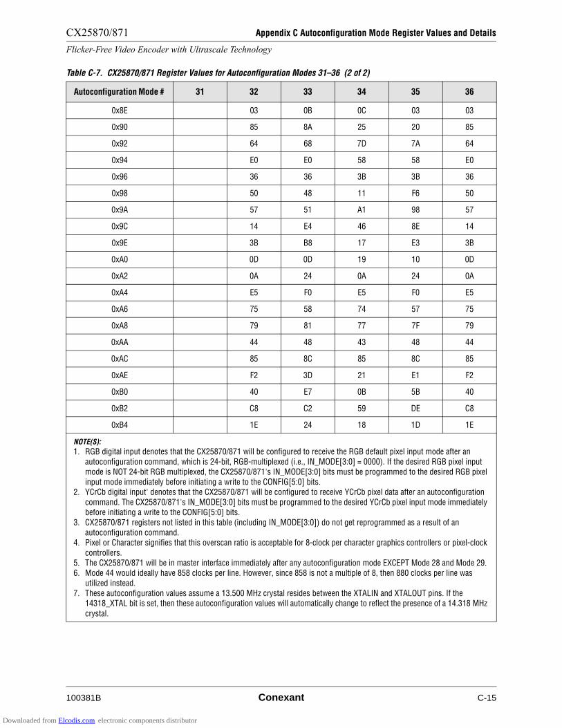
CX25870/871 Appendix C Autoconfiguration Mode Register Values and Details
Flicker-Free Video Encoder with Ultrascale Technology
100381B Conexant C-15
0x8E 03 0B 0C 03 03
0x90 85 8A 25 20 85
0x92 64 68 7D 7A 64
0x94 E0 E0 58 58 E0
0x96 36 36 3B 3B 36
0x98 50 48 11 F6 50
0x9A 57 51 A1 98 57
0x9C 14 E4 46 8E 14
0x9E 3B B8 17 E3 3B
0xA0 0D 0D 19 10 0D
0xA2 0A 24 0A 24 0A
0xA4 E5 F0 E5 F0 E5
0xA6 75 58 74 57 75
0xA8 79 81 77 7F 79
0xAA 44 48 43 48 44
0xAC 85 8C 85 8C 85
0xAE F2 3D 21 E1 F2
0xB0 40 E7 0B 5B 40
0xB2 C8 C2 59 DE C8
0xB4 1E 24 18 1D 1E
NOTE(S):
1. RGB digital input denotes that the CX25870/871 will be configured to receive the RGB default pixel input mode after an autoconfiguration command, which is 24-bit, RGB-multiplexed (i.e., IN_MODE[3:0] = 0000). If the desired RGB pixel input
mode is NOT 24-bit RGB multiplexed, the CX25870/871's IN_MODE[3:0] bits must be programmed to the desired RGB pixel input mode immediately before initiating a write to the CONFIG[5:0] bits.
2. YCrCb digital input' denotes that the CX25870/871 will be configured to receive YCrCb pixel data after an autoconfiguration
command. The CX25870/871's IN_MODE[3:0] bits must be programmed to the desired YCrCb pixel input mode immediately before initiating a write to the CONFIG[5:0] bits.
3. CX25870/871 registers not listed in this table (including IN_MODE[3:0]) do not get reprogrammed as a result of an autoconfiguration command.
4. Pixel or Character signifies that this overscan ratio is acceptable for 8-clock per character graphics controllers or pixel-clock
controllers.5. The CX25870/871 will be in master interface immediately after any autoconfiguration mode EXCEPT Mode 28 and Mode 29.6. Mode 44 would ideally have 858 clocks per line. However, since 858 is not a multiple of 8, then 880 clocks per line was
utilized instead.7. These autoconfiguration values assume a 13.500 MHz crystal resides between the XTALIN and XTALOUT pins. If the
14318_XTAL bit is set, then these autoconfiguration values will automatically change to reflect the presence of a 14.318 MHz
crystal.
Table C-7. CX25870/871 Register Values for Autoconfiguration Modes 31–36 (2 of 2)
Autoconfiguration Mode # 31 32 33 34 35 36
Downloaded from Elcodis.com electronic components distributor
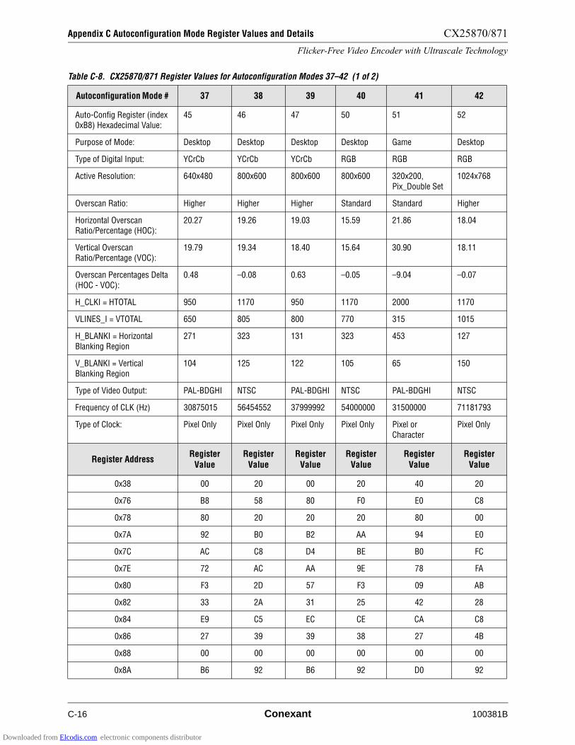
Appendix C Autoconfiguration Mode Register Values and Details CX25870/871
Flicker-Free Video Encoder with Ultrascale Technology
C-16 Conexant 100381B
Table C-8. CX25870/871 Register Values for Autoconfiguration Modes 37–42 (1 of 2)
Autoconfiguration Mode # 37 38 39 40 41 42
Auto-Config Register (index 0xB8) Hexadecimal Value:
45 46 47 50 51 52
Purpose of Mode: Desktop Desktop Desktop Desktop Game Desktop
Type of Digital Input: YCrCb YCrCb YCrCb RGB RGB RGB
Active Resolution: 640x480 800x600 800x600 800x600 320x200,
Pix_Double Set
1024x768
Overscan Ratio: Higher Higher Higher Standard Standard Higher
Horizontal Overscan Ratio/Percentage (HOC):
20.27 19.26 19.03 15.59 21.86 18.04
Vertical Overscan Ratio/Percentage (VOC):
19.79 19.34 18.40 15.64 30.90 18.11
Overscan Percentages Delta
(HOC - VOC):
0.48 –0.08 0.63 –0.05 –9.04 –0.07
H_CLKI = HTOTAL 950 1170 950 1170 2000 1170
VLINES_I = VTOTAL 650 805 800 770 315 1015
H_BLANKI = Horizontal Blanking Region
271 323 131 323 453 127
V_BLANKI = Vertical Blanking Region
104 125 122 105 65 150
Type of Video Output: PAL-BDGHI NTSC PAL-BDGHI NTSC PAL-BDGHI NTSC
Frequency of CLK (Hz) 30875015 56454552 37999992 54000000 31500000 71181793
Type of Clock: Pixel Only Pixel Only Pixel Only Pixel Only Pixel or
Character
Pixel Only
Register AddressRegister
ValueRegister
ValueRegister
ValueRegister
ValueRegister
ValueRegister
Value
0x38 00 20 00 20 40 20
0x76 B8 58 80 F0 E0 C8
0x78 80 20 20 20 80 00
0x7A 92 B0 B2 AA 94 E0
0x7C AC C8 D4 BE B0 FC
0x7E 72 AC AA 9E 78 FA
0x80 F3 2D 57 F3 09 AB
0x82 33 2A 31 25 42 28
0x84 E9 C5 EC CE CA C8
0x86 27 39 39 38 27 4B
0x88 00 00 00 00 00 00
0x8A B6 92 B6 92 D0 92
Downloaded from Elcodis.com electronic components distributor
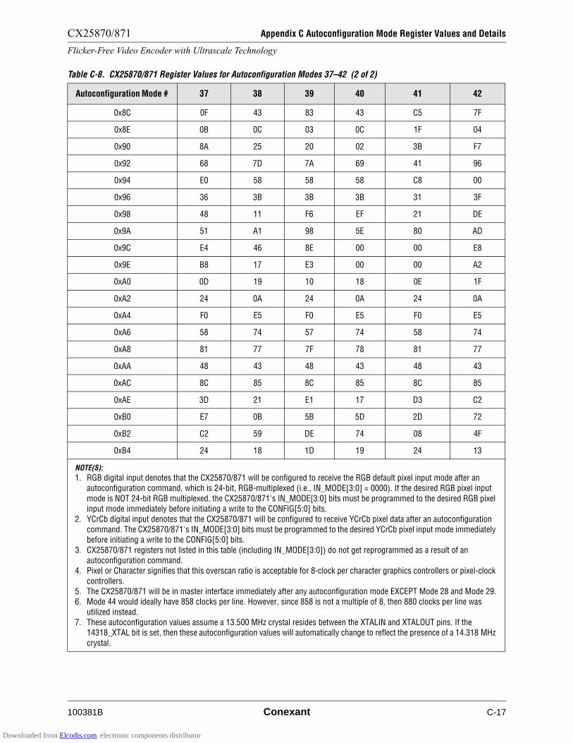
CX25870/871 Appendix C Autoconfiguration Mode Register Values and Details
Flicker-Free Video Encoder with Ultrascale Technology
100381B Conexant C-17
0x8C 0F 43 83 43 C5 7F
0x8E 0B 0C 03 0C 1F 04
0x90 8A 25 20 02 3B F7
0x92 68 7D 7A 69 41 96
0x94 E0 58 58 58 C8 00
0x96 36 3B 3B 3B 31 3F
0x98 48 11 F6 EF 21 DE
0x9A 51 A1 98 5E 80 AD
0x9C E4 46 8E 00 00 E8
0x9E B8 17 E3 00 00 A2
0xA0 0D 19 10 18 0E 1F
0xA2 24 0A 24 0A 24 0A
0xA4 F0 E5 F0 E5 F0 E5
0xA6 58 74 57 74 58 74
0xA8 81 77 7F 78 81 77
0xAA 48 43 48 43 48 43
0xAC 8C 85 8C 85 8C 85
0xAE 3D 21 E1 17 D3 C2
0xB0 E7 0B 5B 5D 2D 72
0xB2 C2 59 DE 74 08 4F
0xB4 24 18 1D 19 24 13
NOTE(S):
1. RGB digital input denotes that the CX25870/871 will be configured to receive the RGB default pixel input mode after an autoconfiguration command, which is 24-bit, RGB-multiplexed (i.e., IN_MODE[3:0] = 0000). If the desired RGB pixel input
mode is NOT 24-bit RGB multiplexed, the CX25870/871's IN_MODE[3:0] bits must be programmed to the desired RGB pixel input mode immediately before initiating a write to the CONFIG[5:0] bits.
2. YCrCb digital input denotes that the CX25870/871 will be configured to receive YCrCb pixel data after an autoconfiguration command. The CX25870/871's IN_MODE[3:0] bits must be programmed to the desired YCrCb pixel input mode immediately before initiating a write to the CONFIG[5:0] bits.
3. CX25870/871 registers not listed in this table (including IN_MODE[3:0]) do not get reprogrammed as a result of an autoconfiguration command.
4. Pixel or Character signifies that this overscan ratio is acceptable for 8-clock per character graphics controllers or pixel-clock
controllers.5. The CX25870/871 will be in master interface immediately after any autoconfiguration mode EXCEPT Mode 28 and Mode 29.6. Mode 44 would ideally have 858 clocks per line. However, since 858 is not a multiple of 8, then 880 clocks per line was
utilized instead.7. These autoconfiguration values assume a 13.500 MHz crystal resides between the XTALIN and XTALOUT pins. If the
14318_XTAL bit is set, then these autoconfiguration values will automatically change to reflect the presence of a 14.318 MHz
crystal.
Table C-8. CX25870/871 Register Values for Autoconfiguration Modes 37–42 (2 of 2)
Autoconfiguration Mode # 37 38 39 40 41 42
Downloaded from Elcodis.com electronic components distributor

Appendix C Autoconfiguration Mode Register Values and Details CX25870/871
Flicker-Free Video Encoder with Ultrascale Technology
C-18 Conexant 100381B
Table C-9. CX25870/871 Register Values for Autoconfiguration Modes 43–47 (1 of 2)
Autoconfiguration Mode # 43 44 45 46 47
Auto-Config Register (index 0xB8) Hexadecimal Value:
53 54 55 56 57
Purpose of Mode: Desktop DVD/noninterlaced
input
Game Desktop for
Brazil
Desktop for
Argentina
Type of Digital Input: RGB RGB RGB RGB RGB
Active Resolution: 1024x768 720x480 320x200,Pixel_Double Set
640x480 640x480
Overscan Ratio: Higher Very Low (DVD Playback)
Standard Standard Standard
Horizontal Overscan
Ratio/Percentage (HOC):
16.20 1.24 20.20 13.79 16.56
Vertical Overscan Ratio/Percentage (VOC):
16.67 1.23 21.40 13.58 16.67
Overscan Percentages Delta (HOC - VOC):
–0.47 0.01 –1.20 0.21 –0.11
H_CLKI = HTOTAL 1410 880 1848 784 944
VLINES_I = VTOTAL 1000 525 275 600 625
H_BLANKI = Horizontal
Blanking Region
337 140 429 126 266
V_BLANKI = Vertical Blanking Region
147 36 43 75 90
Type of Video Output: PAL-BDGHI NTSC NTSC PAL-M (Brazil) PAL-Nc (Argentina)
Frequency of CLK (Hz) 70499989 27692310 30461552 28195793 29500008
Type of Clock: Pixel Only Pixel or Character Pixel or Character Pixel Only Pixel Only
Register AddressRegister
ValueRegister Value Register Value
Register Value
Register Value
0x38 24 00 40 00 00
0x76 C0 E0 90 00 60
0x78 00 D0 80 80 80
0x7A DC 82 90 84 8A
0x7C 08 92 A2 A4 A6
0x7E F0 5C 72 6A 70
0x80 BF 1B CD 7D C1
0x82 2F 13 2B 22 2E
0x84 F1 F2 C2 D4 F2
0x86 4B 26 27 27 27
0x88 00 00 00 00 00
Downloaded from Elcodis.com electronic components distributor

CX25870/871 Appendix C Autoconfiguration Mode Register Values and Details
Flicker-Free Video Encoder with Ultrascale Technology
100381B Conexant C-19
0x8A 82 70 38 10 B0
0x8C 51 8C AD 7E 0A
0x8E 0D 03 1F 03 0B
0x90 E8 0D 13 58 71
0x92 93 24 2B 4B 5A
0x94 00 E0 C8 E0 E0
0x96 3F 36 31 36 36
0x98 33 00 C3 92 00
0x9A A3 50 40 54 50
0x9C 55 C5 D9 0E 72
0x9E 55 4E 89 88 1C
0xA0 1F 0C 0D 0C 0D
0xA2 24 0A 0A 2A 24
0xA4 F0 E5 E5 F0 F0
0xA6 56 76 75 57 57
0xA8 7E 79 78 80 80
0xAA 47 44 44 48 48
0xAC 8C 85 85 8C 8C
0xAE 9B D1 33 6E 1E
0xB0 29 45 28 DB C0
0xB2 26 17 15 76 15
0xB4 18 21 1E 20 1F
NOTE(S):
1. RGB digital input denotes that the CX25870/871 will be configured to receive the RGB default pixel input mode after an autoconfiguration command, which is 24-bit, RGB-multiplexed (i.e., IN_MODE[3:0] = 0000). If the desired RGB pixel input
mode is NOT 24-bit RGB multiplexed, the CX25870/871’s IN_MODE[3:0] bits must be programmed to the desired RGB pixel input mode immediately before initiating a write to the CONFIG[5:0] bits.
2. YCrCb digital input denotes that the CX25870/871 will be configured to receive YCrCb pixel data after an autoconfiguration command. The CX25870/871's IN_MODE[3:0] bits must be programmed to the desired YCrCb pixel input mode immediately before initiating a write to the CONFIG[5:0] bits.
3. CX25870/871 registers not listed in this table (including IN_MODE[3:0]) do not get reprogrammed as a result of an autoconfiguration command.
4. Pixel or Character signifies that this overscan ratio is acceptable for 8-clock per character graphics controllers or pixel-clock
controllers.5. The CX25870/871 will be in master interface immediately after any autoconfiguration mode EXCEPT Mode 28 and Mode 29.6. Mode 44 would ideally have 858 clocks per line. However, since 858 is not a multiple of 8, then 880 clocks per line was
utilized instead.7. These autoconfiguration values assume a 13.500 MHz crystal resides between the XTALIN and XTALOUT pins. If the
14318_XTAL bit is set, then these autoconfiguration values will automatically change to reflect the presence of a 14.318 MHz
crystal.
Table C-9. CX25870/871 Register Values for Autoconfiguration Modes 43–47 (2 of 2)
Autoconfiguration Mode # 43 44 45 46 47
Downloaded from Elcodis.com electronic components distributor
Appendix C Autoconfiguration Mode Register Values and Details CX25870/871
Flicker-Free Video Encoder with Ultrascale Technology
C-20 Conexant 100381B
Downloaded from Elcodis.com electronic components distributor
100381B Conexant D-1
D
Appendix D Closed Caption Pseudo Code
/* Filename: CC_870_Function.C *///Causes CX870/871 encoder to encode 2 bytes of data on every
Odd Field=Field 1
#include stdio.h
#include conio.h
<#include other necessary header files>
char CCdatabyte1, CCdatabyte2; // Define global vari-
ables
//Any graphics controller/MPEG2 Decoder is assumed to be the I2C
master for this design
//Controller/Data Master sends the CX870/871 the digital CC
bytes necessary for encoding into the Composite Video signal or
Luma signal for S-Video output
//H_CLKO[11:0] value should exist in hex format. This register
equals bits3-0 //of register 0x86 and bits 7-0 of register 0x76
870_CCEncoding_onField1(int CCdatabyte1, int CCdatabyte2, int
H_CLKO)
int CBITS, CC_PIPE1, CC_ADD_HEX, CCR_START_HEX, CCSEL,
ReadBit;
int ReadBitArray[8] = 0; //initializes all element of
ReadBitArray to 0
float CC_ADD;
float CCR_START;
CBITS = 17;
CC_PIPE1=60;
CCSEL = 4; //CCSEL[3:0] = 0100 so CC data is
encoded on line 21
//for 525-line systems and line 23 for
625-line systems
//Initialization Section
Write ECCGATE to 1; //this is bit 3 of register C4 for
the CX870/871
//no further closed caption encoding
Downloaded from Elcodis.com electronic components distributor
Appendix D Closed Caption Pseudo Code CX25870/871
Flicker-Free Video Encoder with Ultrascale Technology
D-2 Conexant 100381B
will be performed
//until CCF1B1 & CCF1B2 registers are
again written;
//null will be transmitted on appropriate CC line
in this case
Write ECCF1 to 1; //this is bit 4 of register C4 for
the CX870/871
//Enables CC encoding on Field 1
Write ECCF2 to 0; //this is bit 5 of register C4 for
the CX870/871
//Disables CC encoding for Field 2
if (625LINE == 0) //625LINE = bit 2 of register 0xA2
// 525-line format=NTSC is
being transmitted
//by CX870/871. This assumes
PAL-M = another //525 line
format is not allowed
[equation] CC_ADD = ($pow(2,
CBITS+5)/1716)*1716.0/H_CLKO;
//equation to determine CC_ADD
register for NTSC
CC_ADD_hex =
DEC_TO_HEX_CONVERSION(float CC_ADD);
//assumes
DEC_TO_HEX_CONVERSION
fxn //this should
already exist //some-
where in customers
code
Write CC_ADD(CC_ADD_hex);//CC_ADD[11:0] register is
//comprised of
bits[3:0] of
//register 0xD4
and bits[7:0] of
//CX870/871 reg-
ister 0xD2
[equation] CCR_START =
H_CLKO*10.003*27/1716 + CC_PIPE1;
//eqn to determine CCR_START
register for NTSC
CCR_START_hex = DEC_TO_HEX_CONVERSION(float
CCR_START);
//assumes
DEC_TO_HEX_CONVERSION
Downloaded from Elcodis.com electronic components distributor
CX25870/871 Appendix D Closed Caption Pseudo Code
Flicker-Free Video Encoder with Ultrascale Technology
100381B Conexant D-3
fxn //this should
already exist //some-
where in customers
code
Write CCR_START(CCR_START_hex);
//CCR_START[8:0] reg-
ister is
//comprised of bit[4]
of regis-
ter
//0xD4 and bits[7:0]
of
CX870/871
//register 0xD0
else
// 625-line format = PAL is being transmitted by
CX870/871
//this assumes PAL-M with its 525 line format is
not allowed
[equation] CC_ADD = ($pow(2,
CBITS+5)/1716)*1728.0/H_CLKO;//eqn to determine CC_ADD
register for PAL
CC_ADD_hex =
DEC_TO_HEX_CONVERSION(float CC_ADD);
//assumes DEC_TO_HEX_CONVERSION fxn
//this should already exist //some-
where in customers code
Write CC_ADD(CC_ADD_hex);//CC_ADD[11:0] register is
//comprised of
bits[3:0] of
//register 0xD4
and bits[7:0] of
//CX870/871 reg-
ister 0xD2
[equation] CCR_START =
H_CLKO*10.003*27/1728 + CC_PIPE1;//eqn to determine CCR_START reg-
ister for PAL
CCR_START_hex = DEC_TO_HEX_CONVERSION(float
CCR_START);
//assumes DEC_TO_HEX_CONVERSION fxn
//already exists somewhere in //cus-
tomers code
Downloaded from Elcodis.com electronic components distributor

Appendix D Closed Caption Pseudo Code CX25870/871
Flicker-Free Video Encoder with Ultrascale Technology
D-4 Conexant 100381B
Write CCR_START(CCR_START_hex);
//CCR_START[8:0] reg-
ister is
//comprised of bit[4]
of regis-
ter
//0xD4 and bits[7:0]
of
CX870/871
//register 0xD0
//Previous Initialization Code only needs to be performed once
by I2C master
//Closed Caption Encoding Operation
ReadBitArray[] = CX870ReadbackFxn(ESTATUS = 01);
//CCSTAT_O will be ReadBitArray[3] after this
function executes
Or
ReadBit = ReadCCSTAT_O();//CX870/871 has full readback ability of all bits.
//No longer is it necessary to use legacy Bt869
method of reading //back status bits
if (ReadBitArray[3] == 0)
//alternative IF statement could be if (ReadBit
== 0)
//Closed Caption bytes for Field 1 = Odd Field
have already been //encoded and CCSTAT_O has been
cleared
Write CCF1B1(CCdatabyte1); //assumes CCdatabyte1
is in hex format
//already. Encode new
CC data.
Write CCF1B2(Ccdatabyte2); //assumes CCdatabyte2
is in hex format
//already. Encode new
CC data.
//data is not latched until second of the 2 byte data sequence
is written
//this prevents writing of partial data sequence
//for this reason, data must be written in order of Byte 1 and
then Byte 2
//CCSTAT_O will be automatically be set by the CX870/871 until
CC bytes for odd
//field = Field 1 have been encoded
else
Downloaded from Elcodis.com electronic components distributor
CX25870/871 Appendix D Closed Caption Pseudo Code
Flicker-Free Video Encoder with Ultrascale Technology
100381B Conexant D-5
//CCSTAT_O = 1 because CC data has already been written for
Field 1=ODD field //& has not yet been encoded onto analog video
output signal for the odd field
//CCSTAT_O will be reset immediately after the clock run-in
online 284 for NTSC //and line 335 for PAL
return 0; //CCSTAT_0 = 1 so CC bytes were not encoded
on this pass //through the
869_CCEncoding_onField1 procedure
return 0;
//****************************************************
Bt869ReadbackFxn(int ESTATUS)
//Unlike the previous Conexant VGA encoder, the CX870/871
does have //registers than can be directly read-back. As a
result this //Bt869ReadbackFxn should only be used IF the
software engineer seeks to use //the legacy method of read-
back found in the Bt868/869.
int ReadMONSTAT_CCArray[8] = 0; //entire array now holds 0
Write ESTATUS; //ESTATUS[1:0]= bits 7(MSb) and 6
of register 0xC4 //
ESTATUS[1:0]= 01 from function call.
// 00 and 10 possible for ESTATUS
as well
// yielding different readback
information
Graphics controller issues 0x89 or 0x8B for the CX870/871's
device address;
//no subaddress required here since
the CX870/871
//only has 1 read register to check with the
legacy method
//This step has the effect of reading a single byte
//of data from the CX870/871
//Table 2-2 Readback bit map says
that MONSTAT_A,B,C //bits = bits 7-5
//while Bit 4 = CCSTAT_E, bit 3 =
CCSTAT_O,
// bits 2-0 = FIELD[2:0]
// This ensures the least significant bit of the device
write portion of //the transaction is '1' which indicates
to the encoder that it must //send a byte of data on the
next I2C transaction. Do not write a //subaddress to the
CX870/871(this is not necessary since the CX870/871
//only appears to have 1 read register with the legacy
method) and then //read the "next" byte after the ACK.
Controller_Transmits_I2C_STOP; //I2C Master must issue an
I2C STOP to
Downloaded from Elcodis.com electronic components distributor
Appendix D Closed Caption Pseudo Code CX25870/871
Flicker-Free Video Encoder with Ultrascale Technology
D-6 Conexant 100381B
//finish the Read transac-
tion. An ACK is //not nec-
essary before closing the
//transaction because the
CX870/871 just //ignores
the ACK anyways
return(ReadMONSTAT_CCArray[]);
Downloaded from Elcodis.com electronic components distributor
100381B Conexant E-1
E
Appendix E HDTV Output Mode
NOTE(S): Warning: Conexant is Pursuing Multiple Patents surrounding this Function
E.1 Introduction
A high definition television system can display images that are better than
existing standard definition TV formats such as NTSC, PAL, and SECAM.
HDTV pictures are more true-to-life because the resolution of the TV image is
much higher, and the colors are more accurate.
Many HDTVs are being equipped with a HD Input port that accepts analog
Component YPBPR or analog RGB or both.
Recognizing this fact, Conexant has included an HDTV Output Mode within
the CX25870/871 which generates the analog Component YPBPR or analog RGB
outputs necessary for driving an HDTV’s HD Input port(s).
While in HDTV mode, the device will output either analog RGB or analog
YPBPR signals and automatically insert trilevel synchronization pulses (when
necessary) and vertical synchronizing broad pulses. The output waveforms and
requirements related to the input timing and data on the input side of the
CX25870/871 are explained in this section and in the various SMPTE standards
governing the HDTV resolutions as listed in Table E-5.
Downloaded from Elcodis.com electronic components distributor
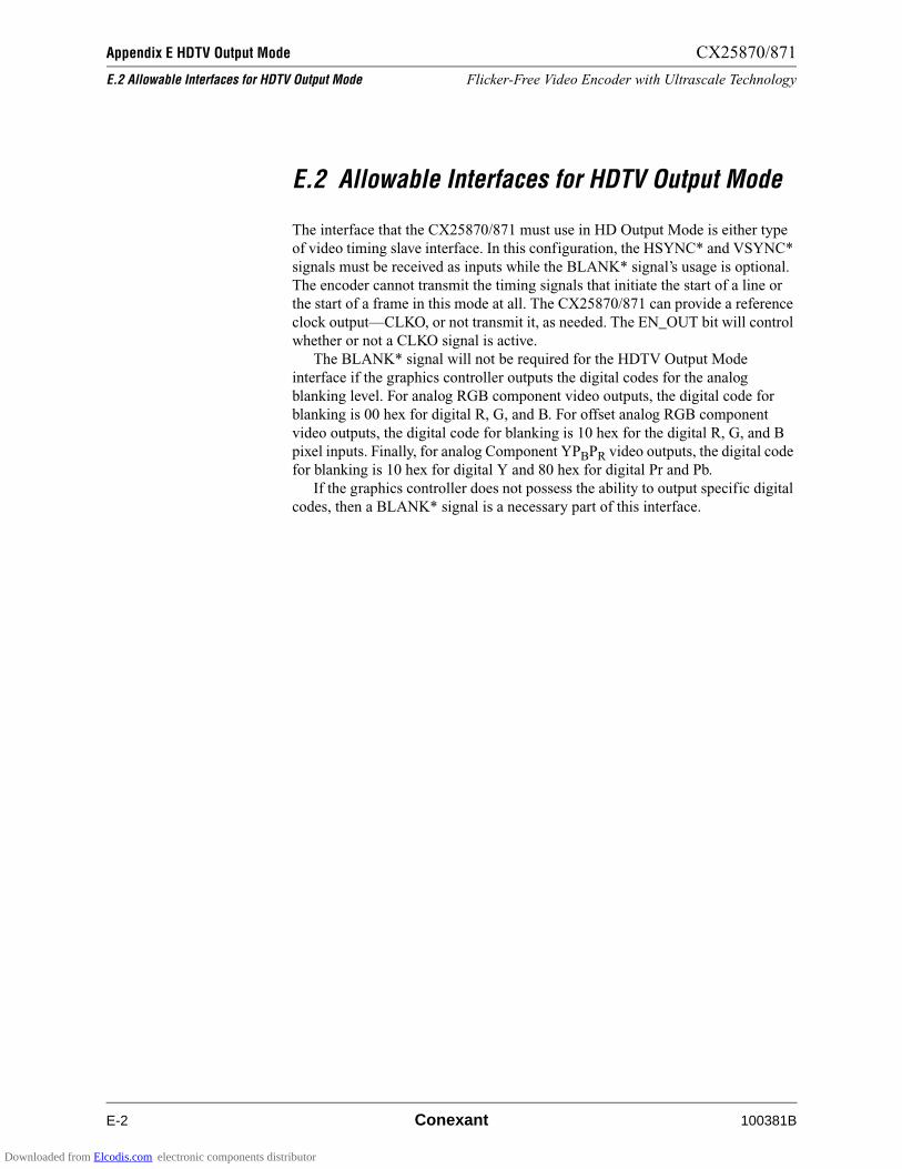
Appendix E HDTV Output Mode CX25870/871
E.2 Allowable Interfaces for HDTV Output Mode Flicker-Free Video Encoder with Ultrascale Technology
E-2 Conexant 100381B
E.2 Allowable Interfaces for HDTV Output Mode
The interface that the CX25870/871 must use in HD Output Mode is either type
of video timing slave interface. In this configuration, the HSYNC* and VSYNC*
signals must be received as inputs while the BLANK* signal’s usage is optional.
The encoder cannot transmit the timing signals that initiate the start of a line or
the start of a frame in this mode at all. The CX25870/871 can provide a reference
clock output—CLKO, or not transmit it, as needed. The EN_OUT bit will control
whether or not a CLKO signal is active.
The BLANK* signal will not be required for the HDTV Output Mode
interface if the graphics controller outputs the digital codes for the analog
blanking level. For analog RGB component video outputs, the digital code for
blanking is 00 hex for digital R, G, and B. For offset analog RGB component
video outputs, the digital code for blanking is 10 hex for the digital R, G, and B
pixel inputs. Finally, for analog Component YPBPR video outputs, the digital code
for blanking is 10 hex for digital Y and 80 hex for digital Pr and Pb.
If the graphics controller does not possess the ability to output specific digital
codes, then a BLANK* signal is a necessary part of this interface.
Downloaded from Elcodis.com electronic components distributor
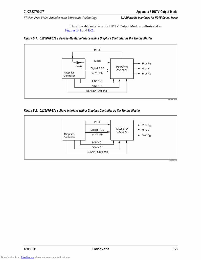
CX25870/871 Appendix E HDTV Output Mode
Flicker-Free Video Encoder with Ultrascale Technology E.2 Allowable Interfaces for HDTV Output Mode
100381B Conexant E-3
The allowable interfaces for HDTV Output Mode are illustrated in
Figures E-1 and E-2.
Figure E-1. CX25870/871’s Pseudo-Master interface with a Graphics Controller as the Timing Master
GraphicsController
Digital RGB
or YPrPb
Clock
Clock
CX25870/CX25871
R or PR
G or Y
B or PB
Delay
HSYNC*
VSYNC*
BLANK* (Optional)
100381_030a
Figure E-2. CX25870/871’s Slave interface with a Graphics Controller as the Timing Master
GraphicsController
Digital RGB
or YPrPb
Clock
CX25870/CX25871
HSYNC*
VSYNC*
BLANK* Optional)
100381_031
R or PR
G or Y
B or PB
Downloaded from Elcodis.com electronic components distributor
Appendix E HDTV Output Mode CX25870/871
E.3 Interface Bit Functionality in HDTV Output Mode: Flicker-Free Video Encoder with Ultrascale Technology
E-4 Conexant 100381B
E.3 Interface Bit Functionality in HDTV Output Mode:
When the CX25870 is transmitting High-Definition Outputs, several interface
bits behave differently than their operation while broadcasting standard-definition
television. These bits and their technical functionality are summarized in the
following list:
• The BLANK* pin must be an input regardless of the slave or
pseudo-master interface. If the blank function is not enabled with the
BLANK* pin, then the BLANK* pin (#38) should be tied high
permanently.
• The EN_BLANKO bit has no effect because the BLANK* signal MUST
be an input. The same rule holds for VGA(R/G/B) – DAC Output
operation.
• The EN_DOT bit has no effect. This bit is related to the standard flicker
filter.
• The FLD_MODE[1:0] bit field has no effect. For 1080i or any other
HD-related interlaced input, VSYNC*'s leading edge must be received
within ±5 clock cycles of the middle of the total line length. For 1080i, this
means the VSYNC* leading edge must be received on any clock period
between the (2200 / 2) ± 5 clocks = 1095th and 1106th clock pulse.
• The polarity reversing bits (HSYNCI, VSYNCI, and BLANKI) perform
the same operations as they do with standard definition outputs.
Downloaded from Elcodis.com electronic components distributor
CX25870/871 Appendix E HDTV Output Mode
Flicker-Free Video Encoder with Ultrascale Technology E.4 Interface Timing between the HDTV Source Device (Master)
100381B Conexant E-5
E.4 Interface Timing between the HDTV Source Device (Master) and CX25870/ CX25871(Timing Slave)
While in HDTV Output Mode, the CX25870/871 encoder should receive
interface signals from the MPEG2 decoder or display processor. The interface
signals that should be shared between the two devices are the HSYNC*,
VSYNC*, BLANK*, CLKI, and Pixel Data lines (P[23:0]). The BLANK* signal
is optional. This signal is only necessary if the data master cannot transmit the
digital codes representing the BLANK levels to the CX25870/871. To reiterate,
the codes for the digital blanking levels of the R, G, B inputs are equal to 00 hex.
The digital codes for blanking change to 10 hex for the R, G, and B pixel inputs if
conversion to offset analog RGB component video outputs is desired. Finally, the
values for digital Y must be 10 hex and for Pr and Pb, digital samples have to
equal 80 hex for the BLANK period for Component Video Out (YPBPR). CLKO
will only be necessary if Pseudo-Master is used as the chosen interface.
To switch the CX25870/871 encoder into HDTV Output mode, the serial
master must program both the OUT_MODE[1:0] bits to 11(DAC Mode) and set
the HDTV_EN bit to 1(bit 7 of the HDTV Register). Immediately after these and
all other steps listed in Table E-1 and Table E-2, the encoder will be set up to
properly generate a set of HDTV Outputs so long as the synchronization, clock,
and data signals are transmitted in accordance with the timing diagrams found at
the back of Appendix E by the master device.
Downloaded from Elcodis.com electronic components distributor
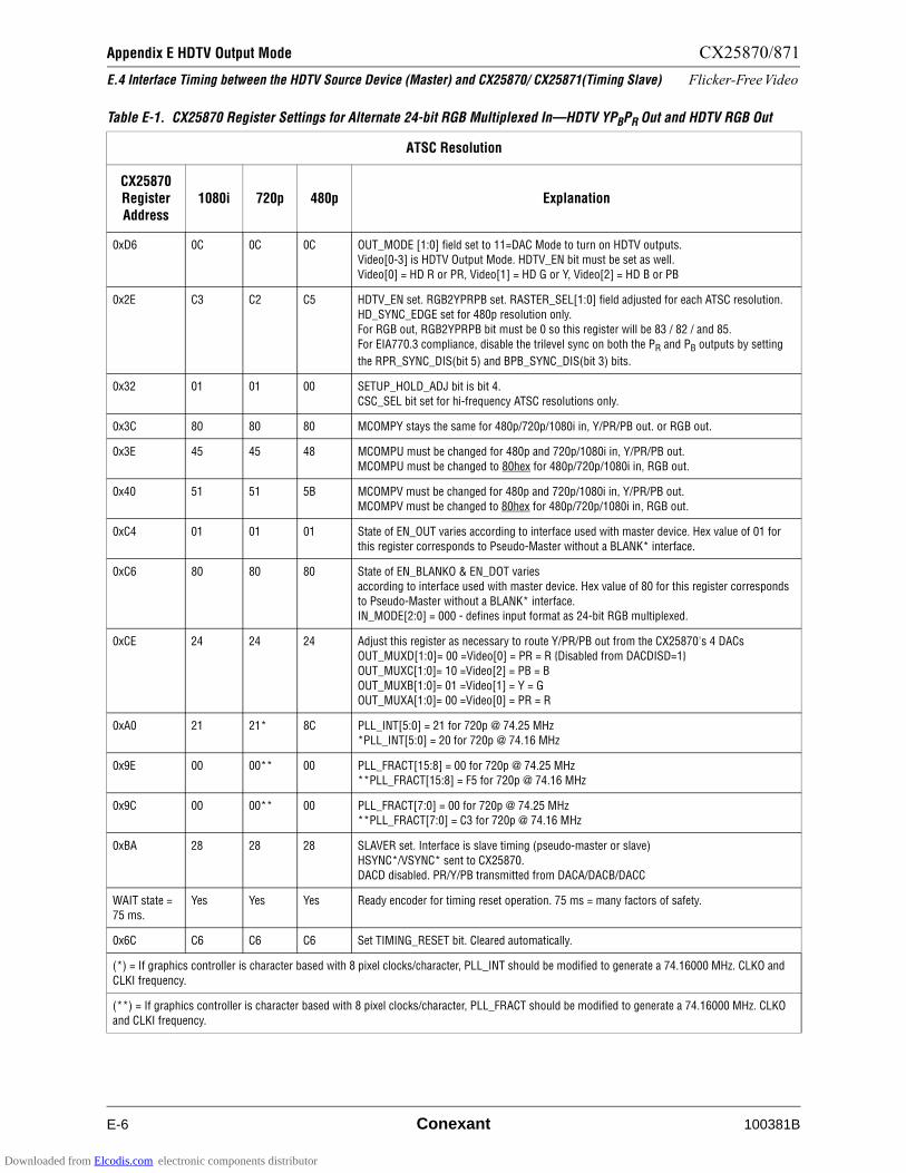
Appendix E HDTV Output Mode CX25870/871
E.4 Interface Timing between the HDTV Source Device (Master) and CX25870/ CX25871(Timing Slave) Flicker-Free Video
E-6 Conexant 100381B
Table E-1. CX25870 Register Settings for Alternate 24-bit RGB Multiplexed In—HDTV YPBPR Out and HDTV RGB Out
ATSC Resolution
CX25870 Register Address
1080i 720p 480p Explanation
0xD6 0C 0C 0C OUT_MODE [1:0] field set to 11=DAC Mode to turn on HDTV outputs.
Video[0-3] is HDTV Output Mode. HDTV_EN bit must be set as well.
Video[0] = HD R or PR, Video[1] = HD G or Y, Video[2] = HD B or PB
0x2E C3 C2 C5 HDTV_EN set. RGB2YPRPB set. RASTER_SEL[1:0] field adjusted for each ATSC resolution.
HD_SYNC_EDGE set for 480p resolution only.
For RGB out, RGB2YPRPB bit must be 0 so this register will be 83 / 82 / and 85.
For EIA770.3 compliance, disable the trilevel sync on both the PR and PB outputs by setting
the RPR_SYNC_DIS(bit 5) and BPB_SYNC_DIS(bit 3) bits.
0x32 01 01 00 SETUP_HOLD_ADJ bit is bit 4.
CSC_SEL bit set for hi-frequency ATSC resolutions only.
0x3C 80 80 80 MCOMPY stays the same for 480p/720p/1080i in, Y/PR/PB out. or RGB out.
0x3E 45 45 48 MCOMPU must be changed for 480p and 720p/1080i in, Y/PR/PB out.
MCOMPU must be changed to 80hex for 480p/720p/1080i in, RGB out.
0x40 51 51 5B MCOMPV must be changed for 480p and 720p/1080i in, Y/PR/PB out.
MCOMPV must be changed to 80hex for 480p/720p/1080i in, RGB out.
0xC4 01 01 01 State of EN_OUT varies according to interface used with master device. Hex value of 01 for
this register corresponds to Pseudo-Master without a BLANK* interface.
0xC6 80 80 80 State of EN_BLANKO & EN_DOT varies
according to interface used with master device. Hex value of 80 for this register corresponds
to Pseudo-Master without a BLANK* interface.
IN_MODE[2:0] = 000 - defines input format as 24-bit RGB multiplexed.
0xCE 24 24 24 Adjust this register as necessary to route Y/PR/PB out from the CX25870's 4 DACs
OUT_MUXD[1:0]= 00 =Video[0] = PR = R Disabled from DACDISD=1
OUT_MUXC[1:0]= 10 =Video[2] = PB = B
OUT_MUXB[1:0]= 01 =Video[1] = Y = G
OUT_MUXA[1:0]= 00 =Video[0] = PR = R
0xA0 21 21* 8C PLL_INT[5:0] = 21 for 720p @ 74.25 MHz
*PLL_INT[5:0] = 20 for 720p @ 74.16 MHz
0x9E 00 00** 00 PLL_FRACT[15:8] = 00 for 720p @ 74.25 MHz
**PLL_FRACT[15:8] = F5 for 720p @ 74.16 MHz
0x9C 00 00** 00 PLL_FRACT[7:0] = 00 for 720p @ 74.25 MHz
**PLL_FRACT[7:0] = C3 for 720p @ 74.16 MHz
0xBA 28 28 28 SLAVER set. Interface is slave timing (pseudo-master or slave)
HSYNC*/VSYNC* sent to CX25870.
DACD disabled. PR/Y/PB transmitted from DACA/DACB/DACC
WAIT state =
75 ms.
Yes Yes Yes Ready encoder for timing reset operation. 75 ms = many factors of safety.
0x6C C6 C6 C6 Set TIMING_RESET bit. Cleared automatically.
(*) = If graphics controller is character based with 8 pixel clocks/character, PLL_INT should be modified to generate a 74.16000 MHz. CLKO and
CLKI frequency.
(**) = If graphics controller is character based with 8 pixel clocks/character, PLL_FRACT should be modified to generate a 74.16000 MHz. CLKO
and CLKI frequency.
Downloaded from Elcodis.com electronic components distributor
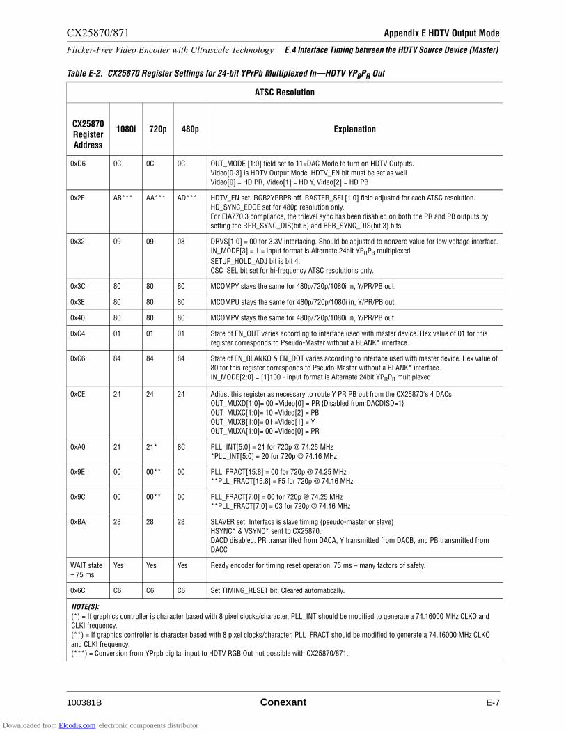
CX25870/871 Appendix E HDTV Output Mode
Flicker-Free Video Encoder with Ultrascale Technology E.4 Interface Timing between the HDTV Source Device (Master)
100381B Conexant E-7
Table E-2. CX25870 Register Settings for 24-bit YPrPb Multiplexed In—HDTV YPBPR Out
ATSC Resolution
CX25870 Register Address
1080i 720p 480p Explanation
0xD6 0C 0C 0C OUT_MODE [1:0] field set to 11=DAC Mode to turn on HDTV Outputs.
Video[0-3] is HDTV Output Mode. HDTV_EN bit must be set as well.
Video[0] = HD PR, Video[1] = HD Y, Video[2] = HD PB
0x2E AB*** AA*** AD*** HDTV_EN set. RGB2YPRPB off. RASTER_SEL[1:0] field adjusted for each ATSC resolution.
HD_SYNC_EDGE set for 480p resolution only.
For EIA770.3 compliance, the trilevel sync has been disabled on both the PR and PB outputs by
setting the RPR_SYNC_DIS(bit 5) and BPB_SYNC_DIS(bit 3) bits.
0x32 09 09 08 DRVS[1:0] = 00 for 3.3V interfacing. Should be adjusted to nonzero value for low voltage interface.
IN_MODE[3] = 1 = input format is Alternate 24bit YPRPB multiplexed
SETUP_HOLD_ADJ bit is bit 4.
CSC_SEL bit set for hi-frequency ATSC resolutions only.
0x3C 80 80 80 MCOMPY stays the same for 480p/720p/1080i in, Y/PR/PB out.
0x3E 80 80 80 MCOMPU stays the same for 480p/720p/1080i in, Y/PR/PB out.
0x40 80 80 80 MCOMPV stays the same for 480p/720p/1080i in, Y/PR/PB out.
0xC4 01 01 01 State of EN_OUT varies according to interface used with master device. Hex value of 01 for this
register corresponds to Pseudo-Master without a BLANK* interface.
0xC6 84 84 84 State of EN_BLANKO & EN_DOT varies according to interface used with master device. Hex value of
80 for this register corresponds to Pseudo-Master without a BLANK* interface.
IN_MODE[2:0] = [1]100 - input format is Alternate 24bit YPRPB multiplexed
0xCE 24 24 24 Adjust this register as necessary to route Y PR PB out from the CX25870's 4 DACs
OUT_MUXD[1:0]= 00 =Video[0] = PR Disabled from DACDISD=1
OUT_MUXC[1:0]= 10 =Video[2] = PB
OUT_MUXB[1:0]= 01 =Video[1] = Y
OUT_MUXA[1:0]= 00 =Video[0] = PR
0xA0 21 21* 8C PLL_INT[5:0] = 21 for 720p @ 74.25 MHz
*PLL_INT[5:0] = 20 for 720p @ 74.16 MHz
0x9E 00 00** 00 PLL_FRACT[15:8] = 00 for 720p @ 74.25 MHz
**PLL_FRACT[15:8] = F5 for 720p @ 74.16 MHz
0x9C 00 00** 00 PLL_FRACT[7:0] = 00 for 720p @ 74.25 MHz
**PLL_FRACT[7:0] = C3 for 720p @ 74.16 MHz
0xBA 28 28 28 SLAVER set. Interface is slave timing (pseudo-master or slave)
HSYNC* & VSYNC* sent to CX25870.
DACD disabled. PR transmitted from DACA, Y transmitted from DACB, and PB transmitted from
DACC
WAIT state
= 75 ms
Yes Yes Yes Ready encoder for timing reset operation. 75 ms = many factors of safety.
0x6C C6 C6 C6 Set TIMING_RESET bit. Cleared automatically.
NOTE(S):
(*) = If graphics controller is character based with 8 pixel clocks/character, PLL_INT should be modified to generate a 74.16000 MHz CLKO and
CLKI frequency.
(**) = If graphics controller is character based with 8 pixel clocks/character, PLL_FRACT should be modified to generate a 74.16000 MHz CLKO
and CLKI frequency.
(***) = Conversion from YPrpb digital input to HDTV RGB Out not possible with CX25870/871.
Downloaded from Elcodis.com electronic components distributor
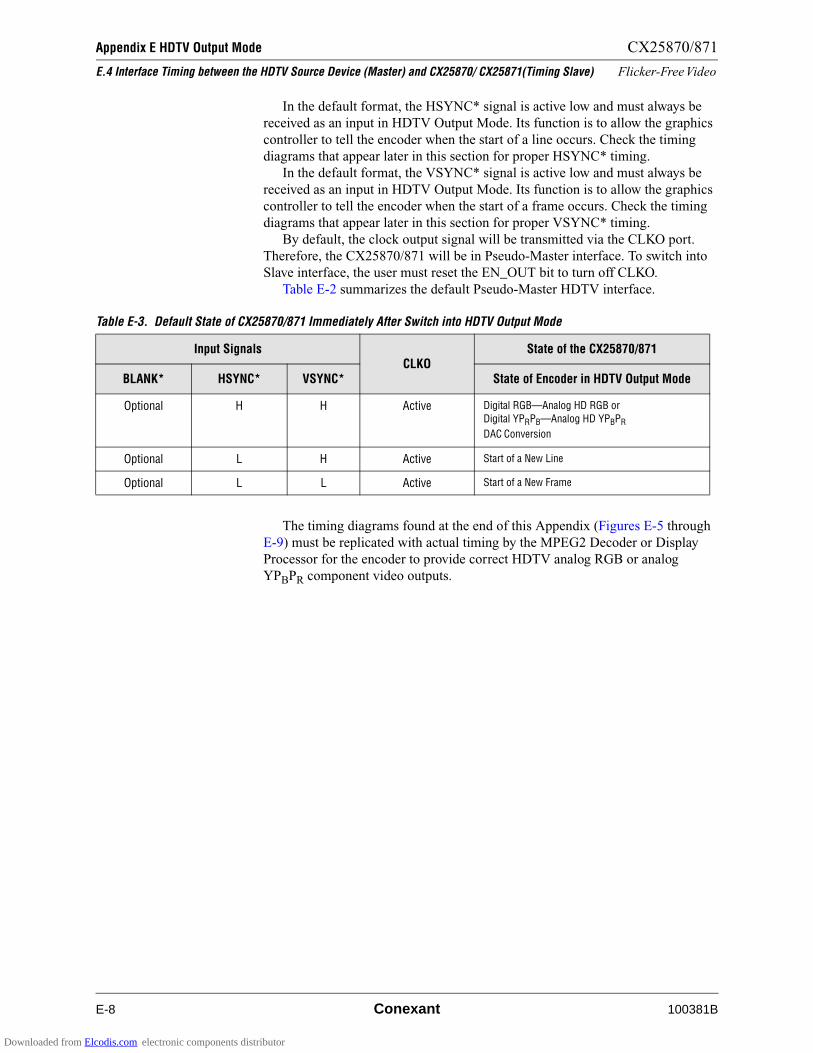
Appendix E HDTV Output Mode CX25870/871
E.4 Interface Timing between the HDTV Source Device (Master) and CX25870/ CX25871(Timing Slave) Flicker-Free Video
E-8 Conexant 100381B
In the default format, the HSYNC* signal is active low and must always be
received as an input in HDTV Output Mode. Its function is to allow the graphics
controller to tell the encoder when the start of a line occurs. Check the timing
diagrams that appear later in this section for proper HSYNC* timing.
In the default format, the VSYNC* signal is active low and must always be
received as an input in HDTV Output Mode. Its function is to allow the graphics
controller to tell the encoder when the start of a frame occurs. Check the timing
diagrams that appear later in this section for proper VSYNC* timing.
By default, the clock output signal will be transmitted via the CLKO port.
Therefore, the CX25870/871 will be in Pseudo-Master interface. To switch into
Slave interface, the user must reset the EN_OUT bit to turn off CLKO.
Table E-2 summarizes the default Pseudo-Master HDTV interface.
The timing diagrams found at the end of this Appendix (Figures E-5 through
E-9) must be replicated with actual timing by the MPEG2 Decoder or Display
Processor for the encoder to provide correct HDTV analog RGB or analog
YPBPR component video outputs.
Table E-3. Default State of CX25870/871 Immediately After Switch into HDTV Output Mode
Input SignalsCLKO
State of the CX25870/871
BLANK* HSYNC* VSYNC* State of Encoder in HDTV Output Mode
Optional H H Active Digital RGB—Analog HD RGB or
Digital YPRPB—Analog HD YPBPR
DAC Conversion
Optional L H Active Start of a New Line
Optional L L Active Start of a New Frame
Downloaded from Elcodis.com electronic components distributor
CX25870/871 Appendix E HDTV Output Mode
Flicker-Free Video Encoder with Ultrascale Technology E.5 Automatic Trilevel Sync Generation
100381B Conexant E-9
E.5 Automatic Trilevel Sync Generation
The CX25870/871 will automatically generate an analog synchronization pulse
with three distinct voltage levels for every leading edge it receives at its HSYNC*
input (so long as RASTER_SEL[1:0] = 10 or 11). This trilevel pulse will be
comprised of a –300 mV LOWSYNC level, a +300 mV HIGHSYNC level, and a
0 mV BLANKING level offset by +350 mVDC because the CX25870/871 cannot
output negative voltages. Figure 3, "Analog and Digital Timing Relationships", of
the SMPTE-274M specification, shows a very detailed diagram of the trilevel
sync and start of a line in 1080i mode. Figure 11 of this same SMPTE standard
illustrates the horizontal timing and trilevel sync in more detail.
For those formats which require trilevel syncs, such as 1080i and 720p, the
timing for certain portions of the synchronization pulses differ slightly. For
instance, the amount of time each pulse is at a voltage level of –300 mV
(LOWSYNC) is not the same from one resolution (ATSC format) to another. For
1080i, the time for the LOWSYNC level each line is 44T(44 clock periods =
44*(1/74.25 MHz)= 592.5 ns For 720p, the same interval is 40T periods long
which equates to 40 * (1/74.25 MHz)= 538.7 ns.
In 480p resolution, in accordance with the SMPTE-293M specification, the
CX25870/871 outputs only bilevel analog synchronization pulses.
As Figure 3 "Analog and Digital Timing Relationships" of the SMPTE-274M
and -296M standards show, the period of time for the HIGHSYNC also varies
when moving from 1080i mode to 720p mode. In this first case, the HIGHSYNC
output level will be active for 44 clock periods. For 1080i, 44 clock periods *
(1/74.25 MHz) = 592.6 ns.
In 720p resolution, the HIGHSYNC output signal will be active for 40 clock
periods per output line. For 720p, 40 clock periods * (1/74.25 MHz)= 538.7ns, so
the HIGHSYNC signal will only be active for 538.7 ns per output line.
Due to these discrepancies, the data master will need to program the
CX25870/871’s RASTER_SEL[1:0] bits properly so the encoder knows exactly
which ATSC format it is going to encode. The encoder will then take care of
outputting the proper analog voltage levels (see Figures E-5 through E-9) for the
appropriate amounts of time depending on the resolution.
Downloaded from Elcodis.com electronic components distributor
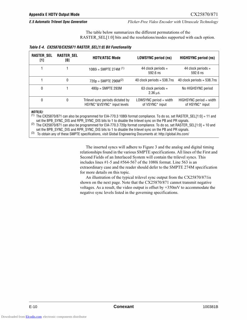
Appendix E HDTV Output Mode CX25870/871
E.5 Automatic Trilevel Sync Generation Flicker-Free Video Encoder with Ultrascale Technology
E-10 Conexant 100381B
The table below summarizes the different permutations of the
RASTER_SEL[1:0] bits and the resolutions/modes supported with each option.
The inserted syncs will adhere to Figure 3 and the analog and digital timing
relationships found in the various SMPTE specifications. All lines of the First and
Second Fields of an Interlaced System will contain the trilevel syncs. This
includes lines #1-5 and #564-567 of the 1080i format. Line 563 is an
extraordinary case and the reader should defer to the SMPTE 274M specification
for more details on this topic.
An illustration of the typical trilevel sync output from the CX25870/871is
shown on the next page. Note that the CX25870/871 cannot transmit negative
voltages. As a result, the video output is offset by +350mV to accommodate the
negative sync levels listed in the governing specifications.
Table E-4. CX25870/CX25871 RASTER_SEL[1:0] Bit Functionality
RASTER_SEL[1]
RASTER_SEL[0]
HDTV/ATSC Mode LOWSYNC period (ns) HIGHSYNC period (ns)
1 1 1080i = SMPTE 274M (1) 44 clock periods =
592.6 ns
44 clock periods =
592.6 ns
1 0 720p = SMPTE 296M(2) 40 clock periods = 538.7ns 40 clock periods = 538.7ns
0 1 480p = SMPTE 293M 63 clock periods =2.36 !s.
No HIGHSYNC period
0 0 Trilevel sync periods dictated by HSYNC*&VSYNC* input levels
LOWSYNC period = width of VSYNC* input
HIGHSYNC period = width of HSYNC* input
NOTE(S):(1) The CX25870/871 can also be programmed for EIA-770.3 1080i format compliance. To do so, set RASTER_SEL[1:0] = 11 and
set the BPB_SYNC_DIS and RPR_SYNC_DIS bits to 1 to disable the trilevel sync on the PB and PR signals.(2) The CX25870/871 can also be programmed for EIA-770.3 720p format compliance. To do so, set RASTER_SEL[1:0] = 10 and
set the BPB_SYNC_DIS and RPR_SYNC_DIS bits to 1 to disable the trilevel sync on the PB and PR signals.(3)
To obtain any of these SMPTE specifications, visit Global Engineering Documents at: http://global.ihs.com/
Downloaded from Elcodis.com electronic components distributor

CX25870/871 Appendix E HDTV Output Mode
Flicker-Free Video Encoder with Ultrascale Technology E.5 Automatic Trilevel Sync Generation
100381B Conexant E-11
Figure E-3. 1080i and 720p Trilevel Sync provided by CX25870/871
44T(for 274M)
44*(1/74.25 MHz) =592.5 ns
44T(for 274M)
44*(1/74.25 MHz) =592.5 ns
44T44*(1/74.25 MHz) =
592.5 ns
70T(for 296M)
70*(1/74.25 MHz) =942.8 ns
650 mV
350 mV
50 mV
40T(for 296M)
40*(1/74.25 MHz) =538.7 ns
40T(for 296M)
40*(1/74.25 MHz) =
Startof the
AnalogLine
538.7 ns
100381_032
NOTE(S):1. Trilevel Sync applies to Y PB, PR output signals as well as HD RGB output signals.2. 720p Trilevel Sync timing differences are listed in RED.
Downloaded from Elcodis.com electronic components distributor
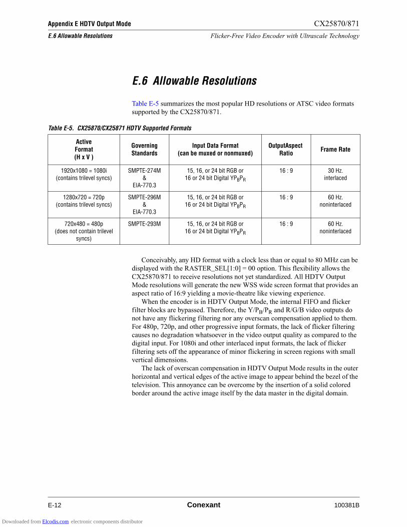
Appendix E HDTV Output Mode CX25870/871
E.6 Allowable Resolutions Flicker-Free Video Encoder with Ultrascale Technology
E-12 Conexant 100381B
E.6 Allowable Resolutions
Table E-5 summarizes the most popular HD resolutions or ATSC video formats
supported by the CX25870/871.
Conceivably, any HD format with a clock less than or equal to 80 MHz can be
displayed with the RASTER_SEL[1:0] = 00 option. This flexibility allows the
CX25870/871 to receive resolutions not yet standardized. All HDTV Output
Mode resolutions will generate the new WSS wide screen format that provides an
aspect ratio of 16:9 yielding a movie-theatre like viewing experience.
When the encoder is in HDTV Output Mode, the internal FIFO and flicker
filter blocks are bypassed. Therefore, the Y/PB/PR and R/G/B video outputs do
not have any flickering filtering nor any overscan compensation applied to them.
For 480p, 720p, and other progressive input formats, the lack of flicker filtering
causes no degradation whatsoever in the video output quality as compared to the
digital input. For 1080i and other interlaced input formats, the lack of flicker
filtering sets off the appearance of minor flickering in screen regions with small
vertical dimensions.
The lack of overscan compensation in HDTV Output Mode results in the outer
horizontal and vertical edges of the active image to appear behind the bezel of the
television. This annoyance can be overcome by the insertion of a solid colored
border around the active image itself by the data master in the digital domain.
Table E-5. CX25870/CX25871 HDTV Supported Formats
Active Format(H x V )
GoverningStandards
Input Data Format(can be muxed or nonmuxed)
Output Aspect Ratio
Frame Rate
1920x1080 = 1080i(contains trilevel syncs)
SMPTE-274M&
EIA-770.3
15, 16, or 24 bit RGB or 16 or 24 bit Digital YPBPR
16 : 9 30 Hz. interlaced
1280x720 = 720p(contains trilevel syncs)
SMPTE-296M&
EIA-770.3
15, 16, or 24 bit RGB or 16 or 24 bit Digital YPBPR
16 : 9 60 Hz. noninterlaced
720x480 = 480p
(does not contain trilevel syncs)
SMPTE-293M 15, 16, or 24 bit RGB or
16 or 24 bit Digital YPBPR
16 : 9 60 Hz.
noninterlaced
Downloaded from Elcodis.com electronic components distributor
CX25870/871 Appendix E HDTV Output Mode
Flicker-Free Video Encoder with Ultrascale Technology E.7 720p Support with Character Clock Based Data Masters
100381B Conexant E-13
E.7 720p Support with Character Clock Based Data Masters
Character clock based graphics controllers with 8 pixel clocks per character will
experience difficulty supporting the 720p ATSC resolution. The reason for this is
because the total line length (i.e., Samples per Total Line = S/TL) of 1650 pixels
for 720P is not evenly divisible by 8. Thus, each line is comprised of an amount of
characters that contains a non-zero fraction (206 + ¼ of a character or 206.25
total characters). To get around this shortcoming, the graphics controller must set
its total line length to 1648 (HTOTAL) pixels and change the pixel clock
frequency to 74.1600 MHz. instead of the values of 1650 pixels and 74.2500
MHz. respectively as specified in the SMPTE-296M standard that governs the
720p resolution.
All of the analog timing will then fall within the guidelines listed in the
SMPTE-296M specification and the CX25870 will generate the desired analog
representation of the 720p ATSC resolution.
Internal analysis of different portions of the 720p R/G/B and Y/PB/PR
waveforms has revealed that this approach is valid. All of the analog timing falls
within the tolerances of the SMPTE-296M standard including the length of the
broad pulse. In terms of clock periods, using the 74.1600 MHz. clock yields a
broad pulse length in time of 20.766 !s in duration. Using a 74.2500 MHz. clock
yields a broad pulse of 20.741 !s in duration. This tiny deviation will not cause a
problem for any High Definition television set.
To change the pixel clock frequency the encoder transmits and expects in
return, the CX25870’s PLL_INT and PLL_FRACT registers must be modified.
For 720p support with Character Clock Based Data Masters, change the
PLL_INT[5:0] bit field from 21 hex (for 74.25 MHz.) to 20hex for 74.1600 MHz.
operation. Furthermore, reduce the 2-byte wide PLL_FRACT[15:0] from 0000
hex (for 74.25 MHz.) to F5C3 hex for 74.1600 MHz. operation. This reduction in
the PLL_INT and PLL_FRACT registers will ensure the encoder transmits the
modified 720p clock of 74.1600 MHz. to the data master through CLKO and
expects to receive data at this frequency coming back (via CLKI). This step must
be done to render 720p via Character Clock Based Data Masters with the
CX25870. Programming the data master’s HTOTAL register to 1648 is vital as
well. Modifying the CX25870’s H_CLKI register to 1648 decimal is optional
because this register will have no effect while the encoder is outputting HDTV.
In summary, for data masters which are character clock based with 8 and 9
pixel clocks per character and wish to support the 720p resolution, slow down the
pixel input clock frequency (CLKI) by 90 kHz. to 74.1600 MHz and compensate
by reducing HTOTAL by 2 pixels per line to 1648 pixels.
Downloaded from Elcodis.com electronic components distributor
Appendix E HDTV Output Mode CX25870/871
E.8 Automatic Insertion of Broad Pulses Flicker-Free Video Encoder with Ultrascale Technology
E-14 Conexant 100381B
E.8 Automatic Insertion of Broad Pulses
In HD televisions, a frame shall begin with five vertical sync lines each
containing a broad pulse. Broad pulses are the HD equivalent to the vertical
synchronizing Serration and Equalization pulses used with present-day analog
TVs. In response to the correct timing provided through the VSYNC* input
which triggers the start of a new frame, the CX25870/871 will automatically
insert broad pulses and trilevel syncs on the first 5 lines of the First Field(#1-#5)
and the first 5 lines in the Second Field (563-568 for 1080i format). These broad
pulses will adhere to the timing and voltage amplitudes found in various SMPTE
specifications.
Figure E-6 illustrates the proper interface timing between the HDTV Source
Device (master) and CX25870/ CX25871(timing slave) during lines that include a
BROAD PULSE in 1080i format. Figure E-8 shows the relationship between the
digital input signals and HDTV output for lines that include a broad pulse in 720p
format.
Downloaded from Elcodis.com electronic components distributor

CX25870/871 Appendix E HDTV Output Mode
Flicker-Free Video Encoder with Ultrascale Technology E.9 HDTV Output Mode Register and Bit Definitions
100381B Conexant E-15
E.9 HDTV Output Mode Register and Bit Definitions
Table E-6. Register Bitmap for HDTV-Specific Registers
8-Bit Address
D7 D6 D5 D4 D3 D2 D1 D0
2E HDTV_EN* RGB2YPRPB* RPR_SYNC
_DIS*
GY_SYNC_
DIS*
BPB_SYNC_
DIS*
HD_SYNC_
EDGE*
RASTER_SEL[1:0]*
32 AUTO_CHK DRVS[1:0] SETUP_HOLD_ADJ
IN_MODE[3] DATDLY_RE OFFSET_RGB*
CSC_SEL*
NOTE(S):
* = HDTV-specific bits
Table E-7. CX25870/871 Registers 0x2E & 0x32–HDTV Output Mode Bit Descriptions (1 of 2)
Bit/Register Names Bit/Register Definition
HDTV_EN Enable HDTV Output Mode. OUT_MODE[1:0] register bits must be set to 11(VGA Mode).
0 = Enables VGA mode. DACs will output analog R, G, B with standard bilevel(–40 IRE) analog syncs.
(DEFAULT)
1 = Enables HDTV Output mode. DACs will output HDTV compatible R/G/B or component video (Y/PR/PB)
outputs. Trilevel syncs and vertical synchronizing/broad pulses will be inserted automatically if
RASTER_SEL[1:0] = nonzero.
Note: EN_SCART bit must be 0 for HDTV Output Mode to be functional.
RGB2YPRPB HDTV output switching bit. This bit is only effective when HDTV_EN = 1 and IN_MODE[3:0] = an RGB Input
format.
0 = Digital RGB Input to Analog HDTV RGB Output (DEFAULT)
1 = Digital RGB Input to Analog HDTV YPRPB Output
RPR_SYNC_DIS 0 = Enables trilevel sync on Red or PR output. (DEFAULT)
1 = Disables trilevel sync on Red or PR output. This bit will have to be set manually for EIA-770.3 compliance.
GY_SYNC_DIS 0 = Enables trilevel sync on Green or Y output. (DEFAULT)
1 = Disables trilevel sync on Green or Y output
BPB_SYNC_DIS 0 = Enables trilevel sync on Blue or PB output. (DEFAULT)
1 = Disables trilevel sync on Blue or PB output. This bit will have to be set manually for EIA-770.3 compliance.
HD_SYNC_EDGE This bit is only effective when HDTV_EN = 1 and RASTER_SEL is nonzero.
0 = Trilevel sync edges transition time is equal to 4 input clocks. (DEFAULT)
1 = Trilevel sync edges transition time is equal to 2 input clocks.
RASTER_SEL[1:0] This bit is only effective when HDTV_EN = 1.
00 = Device does not generate trilevel sync automatically in HDTV output mode. Trilevel sync periods dictated
by active HSYNC* input signal (as HIGHSYNC) and active VSYNC* input signal (as LOWSYNC). (DEFAULT)
01 = Bilevel sync generation for 480P format
10 = Trilevel sync generation for 720P format
11 = Trilevel sync generation for 1080i format
Downloaded from Elcodis.com electronic components distributor
Appendix E HDTV Output Mode CX25870/871
E.9 HDTV Output Mode Register and Bit Definitions Flicker-Free Video Encoder with Ultrascale Technology
E-16 Conexant 100381B
OFFSET_RGB 0 = Standard RGB graphic digital input. Range is 0–255 decimal (DEFAULT)
1 = HDTV OFFSET RGB graphic digital input. Range is 16–235 decimal.
CSC_SEL 0 = Standard color space conversion for RGB to Y (R-Y) (B-Y) based on Y = 0.299R + 0.587G + 0.114B
(DEFAULT)
1 = HDTV color space conversion for RGB to Y (R-Y) (B-Y) based on Y = 0.2126R + 0.7152G + 0.0722B
Table E-7. CX25870/871 Registers 0x2E & 0x32–HDTV Output Mode Bit Descriptions (2 of 2)
Downloaded from Elcodis.com electronic components distributor

CX25870/871 Appendix E HDTV Output Mode
Flicker-Free Video Encoder with Ultrascale Technology E.10 Color Space Conversion Functionality to Support Analog RGB
100381B Conexant E-17
E.10 Color Space Conversion Functionality to Support Analog RGB or YPBPR Component Video Outputs
The CX25870/871 has the ability to receive a digital RGB stream prevalent in
graphics controllers or chipsets with integrated graphics with a width of 15/16/or
24-bits per pixel and transform it to a set of HDTV-compatible analog YPBPR
component video outputs.
The option of not converting the digital RGB stream to analog YPBPR is
available as well. In this case, the CX25870/871 would output a set of
HDTV-compatible analog RGB component video outputs based on the same
15/16/or 24-bits per pixel RGB digital input.
The CX25870/871 can support the conversion from the HDTV
color-difference digital YPBPR color space directly to analog YPBPR component
video outputs seamlessly. No color space conversion nor register reprogramming
is necessary for this case.
However, the HDTV color-difference digital YPBPR color space is slightly
different from the standard digital 4:2:2 YCrCb (i.e., CCIR601) stream found
within consumer applications such as set-top boxes. As a result, the
CX25870/871 must be reprogrammed to new register values not found in
Table E-1 to accommodate for the differences in the two formats. For this
complete register set, contact your local Conexant Field Applications Engineer.
Once obtained, program up the CX25870 as specified and it will provide analog
YPBPR video outputs based on standard 4:2:2 YCrCb MPEG2 input data. The
resulting outputs will be of high quality and viewable on SMPTE274M and
SMPTE 296M standard HDTVs.
For design simplicity, Conexant recommends the data master just send digital
YPRPB for consumer applications instead of YCrCb. For reference these matrix
equations for conversion into digital Pb and digital Pr are listed below:
Pb = 0.5 / (1 – 0.0722) (B’ – Y’)
Where (B’ – Y’) = Cb
Pr = 0.5 / (1 – 0.2126) (R’ – Y’)
Where (R’ – Y’) = Cr
NOTE(S):
1. The CX25870/871’s MCOMPU register must contain a value of 45 hex prior to performing a color space conversion from digital RGB to analog YPBPR. The CX25870/871’s MCOMPV register must contain a value of 51 hex prior to performing a color space
conversion from digital RGB to analog YPBPR.2. Digital Pb and Digital Pr are expressed as P’B and P’R in the SMPTE specifications.
Finally, the CX25870/871 cannot provide analog RGB video outputs from
either color-difference digital YPrPb or 4:2:2 YCrCb MPEG2 input data. The
encoder will not perform this color space conversion whatsoever. For analog RGB
component HD out, a digital RGB input stream must be sent by the data master.
Downloaded from Elcodis.com electronic components distributor

Appendix E HDTV Output Mode CX25870/871
E.11 Recommended Output Filters for HDTV & SDTV Flicker-Free Video Encoder with Ultrascale Technology
E-18 Conexant 100381B
E.11 Recommended Output Filters for HDTV & SDTV
According to the SMPTE274M standard that governs the 1080i ATSC resolution,
“the Y signal for Component HD video output shall have a bandwidth nominally
of 30 MHz. In addition, the PR and PB signals shall have the same bandwidth as
that of the associated Y signal at the analog originating equipment.” Other filter
criteria found in the various SMPTE standards include the amplitude limit for
ripple tolerance in the passband of +/- 0.5 dB relative to insertion loss at 100 kHz.
For Group-Delay, SMPTE states that the ”group delay in the filters (should be)
sufficiently tight to produce good performance while allowing the practical
implementation of the filters themselves" (from SMPTE 274M and
SMPTE293M(720p) standards).
As result of these criteria, during High Definition Output Mode, each
CX25870 DAC output requires a low pass filter with a passband from DC to
30 MHz. while adhering to the aforementioned group delay and passband ripple
tolerances. Unfortunately, the filtering requirements for standard definition
television are quite different in several areas than filtering for HDTV. The most
important difference is that standard definition standards such as NTSC, PAL,
and SECAM require a much lower 8 MHz. passband starting at DC than HDTV.
This bandwidth difference coupled with the differing voltage amplitudes of
the signals themselves forced Conexant to design a new low pass filter with a
wider passband to accommodate the HD outputs. After extensive testing and
cost/benefit trade-offs, the company recommends that any customer using the
encoder for both its standard definition and high definition capabilities design-in
the low pass filter found in Figure E-4. This filter has been shown to exhibit many
of the desired roll off, ripple, and passband characteristics defined in the
aforementioned SMPTE standards.
Downloaded from Elcodis.com electronic components distributor
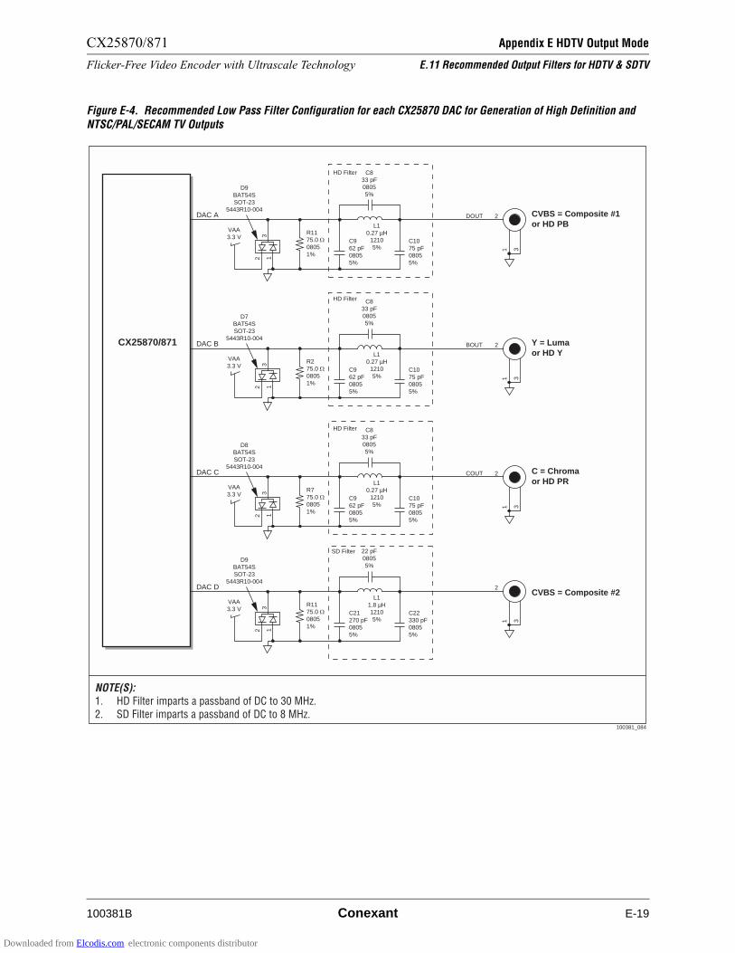
CX25870/871 Appendix E HDTV Output Mode
Flicker-Free Video Encoder with Ultrascale Technology E.11 Recommended Output Filters for HDTV & SDTV
100381B Conexant E-19
Figure E-4. Recommended Low Pass Filter Configuration for each CX25870 DAC for Generation of High Definition and NTSC/PAL/SECAM TV Outputs
100381_084
CX25870/871
DAC DCVBS = Composite #2
VAA3.3 V
123
1
2
3
D9BAT54SSOT-23
5443R10-004
R1175.0 "08051%
SD Filter
HD Filter
HD Filter
HD Filter
C21270 pF08055%
22 pF08055%
C22330 pF08055%
L11.8 µH12105%
DAC B Y = Lumaor HD Y
VAA3.3 V
123
1
2
3
D7BAT54SSOT-23
5443R10-004
R275.0 "08051%
C962 pF08055%
C833 pF08055%
C1075 pF08055%
BOUT
L10.27 µH
12105%
DAC C C = Chromaor HD PR
VAA3.3 V
123
1
2
3
D8BAT54SSOT-23
5443R10-004
R775.0 "08051%
C962 pF08055%
C833 pF08055%
C1075 pF08055%
COUT
L10.27 µH
12105%
DAC A CVBS = Composite #1or HD PB
VAA3.3 V
123
1
2
3
D9BAT54SSOT-23
5443R10-004
R1175.0 "08051%
C962 pF08055%
C833 pF08055%
C1075 pF08055%
DOUT
L10.27 µH
12105%
NOTE(S):1. HD Filter imparts a passband of DC to 30 MHz.2. SD Filter imparts a passband of DC to 8 MHz.
Downloaded from Elcodis.com electronic components distributor

Appendix E HDTV Output Mode CX25870/871
E.12 Timing Diagrams for HDTV Output Mode Flicker-Free Video Encoder with Ultrascale Technology
E-20 Conexant 100381B
E.12 Timing Diagrams for HDTV Output Mode
Review the next five pages (Figures E-4 through E-8) for illustrations of the
relationship between the digital inputs received by the CX25870/871 and the
HDTV Output signals transmitted by the encoder while in HDTV Output Mode.
Downloaded from Elcodis.com electronic components distributor
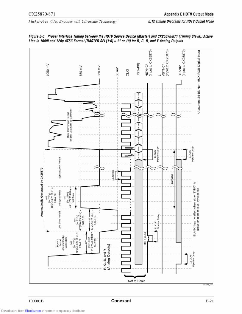
CX25870/871 Appendix E HDTV Output Mode
Flicker-Free Video Encoder with Ultrascale Technology E.12 Timing Diagrams for HDTV Output Mode
100381B Conexant E-21
Figure E-5. Proper Interface Timing between the HDTV Source Device (Master) and CX25870/871 (Timing Slave): Active Line in 1080i and 720p ATSC Format (RASTER SEL[1:0] = 11 or 10) for R, G, B, and Y Analog Outputs
100381_067
. . .
.
. . .
. .. .
. .
BLA
NK
Per
iod
(Gen
erat
ed b
yC
ontr
olle
r)
70T
(for
720
p)70
*(1/
74.2
5 M
Hz)
=94
2.8
ns
44T
(for
108
0i)
44*(
1/74
.25
MH
z) =
592.
5 ns
44T
(for
108
0i)
44*(
1/74
.25
MH
z) =
592.
5 ns
40T
(for
720
p)40
*(1/
74.2
5 M
Hz)
=53
8.7
ns
40T
(for
720
p)40
*(1/
74.2
5 M
Hz)
=53
8.7
ns
44T
44*(
1/74
.25
MH
z) =
592.
5 ns
Low
Syn
c P
erio
dH
i-Syn
c P
erio
dS
ync
BLA
NK
Per
iod
RG
B C
onve
rsio
n P
erio
d(D
igita
l Dat
a S
ent b
y C
ontr
olle
r
13.4
68 n
s.
11 C
LKP
ipel
ine
Del
ay11
CLK
Pip
elin
e D
elay
11 C
LKs
Pip
elin
e D
elay
Min
. 4 C
LKs
132
CLK
s
11 C
LKP
ipel
ine
Del
ay
RG
B1
RG
B2
RG
B3
RG
B4
RG
B5
RG
B6
RG
B7
RG
B8
RG
B9
Au
tom
atic
ally
Gen
erat
ed b
y C
X25
870
BLA
NK
* ha
s no
effe
ct w
hen
eith
er S
YN
C*
isac
tive
or in
the
tri-l
evel
syn
c pe
riod
R, G
, B, a
nd
Y(A
nal
og
Ou
tpu
ts)
650
mV
350
mV
50 m
V
CLK
I
[P23
–P0]
HS
YN
C*
(Inp
ut to
CX
2587
0)
1 VS
YN
C*
(Inp
ut to
CX
2587
0)
BLA
NK
*(I
nput
to C
X25
870)
1050
mV
*Ass
umes
24-
Bit
Non
-MU
X R
GB
Dig
ital I
nput
Not to Scale
Downloaded from Elcodis.com electronic components distributor
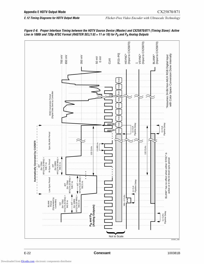
Appendix E HDTV Output Mode CX25870/871
E.12 Timing Diagrams for HDTV Output Mode Flicker-Free Video Encoder with Ultrascale Technology
E-22 Conexant 100381B
Figure E-6. Proper Interface Timing between the HDTV Source Device (Master) and CX25870/871 (Timing Slave): Active Line in 1080i and 720p ATSC Format (RASTER SEL[1:0] = 11 or 10) for PB and PR Analog Outputs
100381_068
Not to Scale
. . .
.
. . .
. .. .
. .
BLA
NK
Per
iod
(Gen
erat
ed b
yC
ontr
olle
r)
70T
(for
720
p)70
*(1/
74.2
5 M
Hz)
=94
2.8
ns
44T
(for
108
0i)
44*(
1/74
.25
MH
z) =
592.
5 ns
44T
(for
108
0i)
44*(
1/74
.25
MH
z) =
592.
5 ns
40T
(for
720
p)40
*(1/
74.2
5 M
Hz)
=53
8.7
ns
40T
(for
720
p)40
*(1/
74.2
5 M
Hz)
=53
8.7
ns
44T
44*(
1/74
.25
MH
z) =
592.
5 ns
Low
Syn
c P
erio
dH
i-Syn
c P
erio
dS
ync
BLA
NK
Per
iod
RG
B C
onve
rsio
n P
erio
d(D
igita
l Dat
a S
ent b
y C
ontr
olle
r
13.4
68 n
s.
11 C
LKP
ipel
ine
Del
ay11
CLK
Pip
elin
e D
elay
11 C
LKs
Pip
elin
e D
elay
Min
. 4 C
LKs
132
CLK
s
11 C
LKP
ipel
ine
Del
ay
RG
B1
RG
B2
RG
B3
RG
B4
RG
B5
RG
B6
RG
B7
RG
B8
RG
B9
Au
tom
atic
ally
Gen
erat
ed b
y C
X25
870
BLA
NK
* ha
s no
effe
ct w
hen
eith
er S
YN
C*
isac
tive
or in
the
tri-l
evel
syn
c pe
riod
PB
an
d P
R(A
nal
og
Ou
tpu
ts)
650
mV
350
mV
50 m
V0
mV
CLK
I
[P23
–P0]
HS
YN
C*
(Inp
ut to
CX
2587
0)
1 VS
YN
C*
(Inp
ut to
CX
2587
0)
BLA
NK
*(I
nput
to C
X25
870)
700
mV
*Ass
umes
24-
Bit
Non
-MU
X R
GB
Dig
ital I
nput
with
Col
or S
pace
Con
vers
ion
Don
e In
tern
ally
132
CLK
s
Downloaded from Elcodis.com electronic components distributor

CX25870/871 Appendix E HDTV Output Mode
Flicker-Free Video Encoder with Ultrascale Technology E.12 Timing Diagrams for HDTV Output Mode
100381B Conexant E-23
Figure E-7. Proper Interface Timing between the HDTV Source Device (Master) and CX25870/871 (Timing Slave): Broad Pulse Line in 1080i ATSC Format (RASTER SEL[1:0] = 11)—Odd Field
. . .
.
BLA
NK
Per
iod
(Gen
erat
ed b
yC
ontr
olle
r)
44T
(for
108
0i)
44*(
1/74
.25
MH
z) =
592.
5 ns
44T
(for
108
0i)
44*(
1/74
.25
MH
z) =
592.
5 ns
44T
44*(
1/74
.25
MH
z) =
592.
5 ns
Low
Syn
c P
erio
dH
i-Syn
c P
erio
dB
LAN
K P
erio
d
11 C
LKP
ipel
ine
Del
ay
11 C
LKP
ipel
ine
Del
ay
Min
. 4 C
LKs
(An
alo
g O
utp
uts
) Min
. 4 C
LKs
11 C
LKP
ipel
ine
Del
ay11
CLK
Pip
elin
e D
elay
Au
tom
atic
ally
Gen
erat
ed b
y C
X25
870
Bro
ad P
ulse
Per
iod
(Gen
erat
ed b
y C
X25
870
En
cod
er)
BLA
NK
* ha
s no
effe
ct w
hen
eith
er S
YN
C*
isac
tive
or in
the
tri-l
evel
syn
c pe
riod
R, G
, B, a
nd
Y, P
BP
R
650
mV
350
mV
50 m
V
[P23
–P0]
HS
YN
C*
(Inp
ut to
CX
2587
0)
1 VS
YN
C*
(Inp
ut to
CX
2587
0)
BLA
NK
*(I
nput
to C
X25
870)
700
mV
NO
TE(S
):a.
CX
25
87
0/8
71
au
tom
atic
ally
gen
erat
es a
BR
OA
D P
UL
SE
leve
ls a
nd
tim
ing
.If
a B
LA
NK
* s
ign
al is
no
t u
sed
, ad
her
e to
no
tes
b.
and
c.
b.
R,
G,
B,
and
Y d
igit
al s
amp
les
hav
e to
eq
ual
00
hex
= 0
dec
imal
fo
r th
e B
LA
NK
Per
iod
.c.
Pr
and
Pb
dig
ital
sam
ple
s h
ave
to e
qu
al 8
0 h
ex =
12
8 d
ecim
al f
or
the
BL
AN
K P
erio
d.
Tim
e sc
ale
com
pres
sed.
100381_069
Downloaded from Elcodis.com electronic components distributor
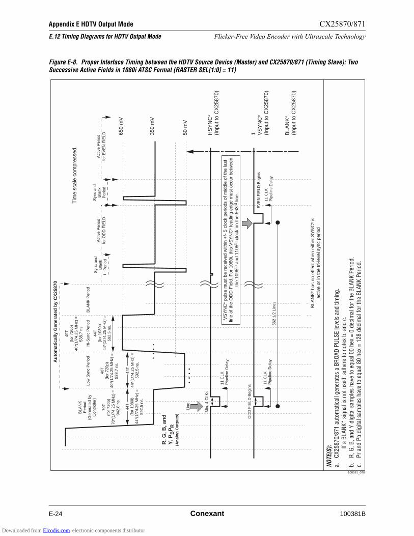
Appendix E HDTV Output Mode CX25870/871
E.12 Timing Diagrams for HDTV Output Mode Flicker-Free Video Encoder with Ultrascale Technology
E-24 Conexant 100381B
Figure E-8. Proper Interface Timing between the HDTV Source Device (Master) and CX25870/871 (Timing Slave): Two Successive Active Fields in 1080i ATSC Format (RASTER SEL[1:0] = 11)
NO
TE(S
):a.
CX
2587
0/87
1 au
tom
atic
all g
ener
ates
a B
RO
AD
PU
LSE
leve
ls a
nd t
imin
g.If
a B
LAN
K*
sign
al is
not
use
d, a
dher
e to
not
es b
. an
d c.
b.R
, G
, B
, an
d Y
dig
ital s
ampl
es h
ave
to e
qual
00
hex
= 0
deci
mal
for
the
BLA
NK
Per
iod.
c.P
r an
d P
b di
gita
l sam
ples
hav
e to
equ
al 8
0 he
x =
128
deci
mal
for
the
BLA
NK
Per
iod.
100381_070
. . .
.
. . .
.
BLA
NK
Per
iod
(Gen
erat
ed b
yC
ontr
olle
r)
70T
(for
720
p)70
*(1/
74.2
5 M
Hz)
=94
2.8
ns.
44T
(for
108
0i)
44*(
1/74
.25
MH
z) =
592.
5 ns
.
44T
(for
108
0i)
44*(
1/74
.25
MH
z) =
592.
5 ns
.
40T
(for
720
p)40
*(1/
74.2
5 M
Hz)
=53
8.7
ns.
40T
(for
720
p)40
*(1/
74.2
5 M
Hz)
=53
8.7
ns.
44T
44*(
1/74
.25
MH
z) =
592.
5 ns
.
Low
Syn
c P
erio
dH
i-Syn
c P
erio
dB
LAN
K P
erio
d
Act
ive
Per
iod
for
OD
D F
IELD
Syn
c an
dB
lank
Per
iod
Act
ive
Per
iod
for
EV
EN
FIE
LD
11 C
LKP
ipel
ine
Del
ay
11 C
LKP
ipel
ine
Del
ay11
CLK
Pip
elin
e D
elay
Min
. 4 C
LKs
562
1/2
Line
s
Line
(Ana
log
Out
puts
)
OD
D F
IELD
Beg
ins
EV
EN
FIE
LD B
egin
s
Aut
omat
ical
ly G
ener
ated
by
CX
2587
0
BLA
NK
* ha
s no
effe
ct w
hen
eith
er S
YN
C*
isac
tive
or in
the
tri-l
evel
syn
c pe
riod
VS
YN
C*
puls
e m
ust b
e re
ceiv
ed w
ithin
+/-
5 c
lock
per
iods
of m
iddl
e of
the
last
line
of th
e O
DD
Fie
ld. F
or 1
080i
, thi
s V
SY
NC
* le
adin
g ed
ge m
ust o
ccur
bet
wee
nth
e 10
95th
and
110
5th
cloc
k on
the
563r
d lin
e.
R, G
, B, a
ndY
, PB
PR
650
mV
350
mV
50 m
V
HS
YN
C*
(Inp
ut to
CX
2587
0)
1 VS
YN
C*
(Inp
ut to
CX
2587
0)
BLA
NK
*(I
nput
to C
X25
870)
Tim
e sc
ale
com
pres
sed.
Syn
c an
dB
lank
Per
iod
Downloaded from Elcodis.com electronic components distributor

CX25870/871 Appendix E HDTV Output Mode
Flicker-Free Video Encoder with Ultrascale Technology E.12 Timing Diagrams for HDTV Output Mode
100381B Conexant E-25
Figure E-9. Proper Interface Timing between the HDTV Source Device (Master) and CX25870/871 (Timing Slave): Broad Pulse Line in 720p ATSC Format (RASTER SEL[1:0] = 10)
650
mV
350
mV
50 m
V
CLK
I
[P23
–P0]
HS
YN
C*
(Inp
ut to
CX
2587
0)
1 VS
YN
C*
(Inp
ut to
CX
2587
0)
. . .
.
BLA
NK
Per
iod
(Gen
erat
ed b
yC
ontr
olle
r)
70T
(for
720
p)70
*(1/
74.2
5 M
Hz)
=94
2.8
ns
70T
40T
(for
720
p)40
*(1/
74.2
5 M
Hz)
=53
8.7
ns
40T
(for
720
p)40
*(1/
74.2
5 M
Hz)
=53
8.7
ns
44T
Low
Syn
c P
erio
dH
i-Syn
c P
erio
dB
LAN
K P
erio
d
11 C
LKP
ipel
ine
Del
ay
11 C
LKP
ipel
ine
Del
ay
Min
. 4 C
LKs
Min
. 4 C
LKs
Aut
omat
ical
ly G
ener
ated
by
CX
2587
0
Bro
ad P
ulse
Per
iod
(Gen
erat
ed b
y C
X25
870
Enc
oder
)
BLA
NK
* ha
s no
effe
ct w
hen
eith
er S
YN
C*
isac
tive
or in
the
tri-l
evel
syn
c pe
riod
(Ana
log
Out
puts
)
R, G
, B, a
ndY
, PB
PR
700
mV
100381_071a
NO
TE(S
):a.
CX
2587
0/87
1 au
tom
atic
ally
gen
erat
es a
BR
OA
D P
ULS
E le
vel a
nd t
imin
g.
I
f a
BLA
NK
* si
gnal
is n
ot u
sed,
adh
ere
to n
otes
b. a
nd c
.b.
R, G
, B, a
nd Y
dig
ital s
ampl
es h
ave
to e
qual
00
hex
= 0
deci
mal
for
the
BLA
NK
Per
iod.
c.P
r an
d P
b di
gita
l sam
ples
hav
e to
equ
al 8
0 he
x =
128
deci
mal
for
the
BLA
NK
Per
iod.
Downloaded from Elcodis.com electronic components distributor

Appendix E HDTV Output Mode CX25870/871
E.12 Timing Diagrams for HDTV Output Mode Flicker-Free Video Encoder with Ultrascale Technology
E-26 Conexant 100381B
Downloaded from Elcodis.com electronic components distributor

www.conexant.com
General Information:
U.S. and Canada: (800) 854-8099
International: (949) 483-6996
Headquarters – Newport Beach
4311 Jamboree Rd.
Newport Beach, CA. 92660-3007
Downloaded from Elcodis.com electronic components distributor