photonics in switching
TRANSCRIPT
Photonics in Switching We may not have pure photonic switching by the year 2000, but the new millenium's broadband hardware cannot be connected without photonic help. m m m m m m m m m m m
H. Scott Hinton
,
ne of t he keys t o the fu tu re of telecommunications companies will be their ability to provide new broadband services t o both the business communitv and the resi-
dential customer. These new services include the transport of National Television Standards Com- mittee (NTSC) video, enhanced quality television (EQTV), high-definition television (HDTV), switched video, high-data-rate file transfers, information retrieval, and animatedgraphics, in addi- tion to being an interconnect for diskless work- stations and local area networks/metropolitan area networks (LANs/MANs) [l]. With these new services will come the need for the equivalent of a broadband switching office. Such a system could requi re the capability of supporting in excess of 10,000 users with broadband channel bit rates exceeding 100 Mb/s. This implies a switch- ing fabric the aggregate bit rate of which could be greater than 1 Tb/s. This fabric. or collection of different fabrics, could have to support both the con- ventional circuit-switching capabilities, as they currently exist on the network, and control packet services, such as ATM cells embedded in Synchronous Optical NETwork (SONET) streamsof data, at per- port costs similar to existing plain old telephone ser- vice (POTS). The hope of photonic systems is that, through the application of either the tempo- ral or spatial bandwidth available in the photonic domain and the new architectures and fabrics that are conceived, these broadband systems and ser- vices will be economically realized [2].
Strengths of the Optical Domain esearch in photonic switching fabrics can be R categorized as systems based on either guid-
ed-wave or free-space optics. Typically, guided-wave optics have been concerned with the application of optical fiber and the utilization of the large temporal bandwidth available in guided-wave struc- tures such as optical fiber, star couplers [3], and direc- tional couplers [4]. This bandwidth transparency provides large- bandwidth analog channels, which can be used to transport many channels of digital
H. SCOTT HINTON is head of the Photonic Switching Department atAT&TBell Laboratories.
information. As an example, current single-mode optical fiber supports approximately 25 THz of com- munications bandwidth around the 1.5 Fm wave- length region. This offers the opportunity to multiplex many users, through either time division or spec- tral division, onto a single-mode fiber, thus reduc- ing the cost pe r user of t he requi red system hardware. Therefore, researchers have pursued both time-based switching fabrics (photonic time-slot interchangers and multiple access schemes such as time-division multiple access and code- divi- sion multiple access), and wavelength-based fab- rics (wavelength in te rchangers and both wavelength-division multiple access and spectral code-division multiple access). Arguments for guid- ed-wave optics include:
Natural evolution from today's electrical tech- nology, since it can integrate directly with elec- trical transmission lines Building on the existing fiber base present in the telecommunications network Many guided-wave optically transparent devices demonstrated in the laboratory Supporting optically transparent switching fabrics More developed and better understood technology than the free-space technology Free-space optics, on the other hand, has been
more concernedwith using the available spatial band- width to increase the intrasystem connectivity and reduce the limiting effects of buses, low pin-out inte- gra ted circuits ( ICs) , p r in ted circuit boa rds (PCBs), and multi-chip modules (MCMs). This approach is more concerned with extending the life of the electronics technology through the use of optical pin-outs and/or interconnects than replac- ing it. This new technology could be an important aid to electronics technology, since many of the high- performance high-density integrated circuits are pin- out-limited. This pin-out limitation forces unnatural system partitioning and limits architectural con- siderations in both computing and switching systems. Although there has been considerable progress in electronic packaging, such as C4 (flip-chip) and TAB bonding techniques [ 5 ] , using light as a communi- cations medium may be preferred, because light has been shown to be more energy-efficient when
1055-6877/92/$03.00 19920 IEEE IEEE LTS August 1992 26
- 1
Authorized licensed use limited to: Utah State University. Downloaded on June 14,2010 at 19:07:52 UTC from IEEE Xplore. Restrictions apply.
the distance between communicating elements is greaterthan 1 mm. Workin this research arearanges from PCB-to-PCB interconnects to gate-to-gate interconnection of optical logic gates.
Research in free-space optics has been focused on multi-stage space-division switching fabrics, par- ticularly large-dimension fabrics, where the need for a large number of connections is evident. The exper- imental work done to date has used symmetric SEED (S-SEED) arrays [6] as the switching nodes in the network, with bulk optical elements providing the optical interconnects required by the multi- stage networks. Other proposed switching nodes for these fabrics include other optical logicgates, such as opti- cal logic etalons (OLEs) [7 ] , nonlinear interfer- ence filters (NLIFs) [8], double heterostructure optoelectronic switches (DOESs) [9], vertical sur- face transmission electro-photonic (VSTEP) device arrays [ 101, o r 2-D arrays of “smart pixels” in which the functionality of many nodes are integrated onto a single electronic IC [l l] . Due to the poten- tial large-scale integration of the switching nodes on each array ( u p t o 104 nodes p e r a r ray) , this approach should eventually reduce the hardware cost of such a fabric and provide the capability of implementing a large-dimension switching fabric that could be used as either a packet or time-mul- tiplexed switch. Leading-edge research in this area is currently exploring both the performance and cost issuesassociatedwithswitchingfabrics as afunc- tion of the granularity of the optical intercon- nects and the intelligence of the nodes. The potential advantages of this free-space interconnect technology include:
Providing another dimension of freedom in rout-
Potentially provides high integration density. Providing low power dissipation per pin-out. Inherent parallel structures can reduce latency. Through the development of new architectures and fabrics utilizing t h e parallelism of t h e available spatial bandwidth, new high-perfor- mance low-cost systems could emerge.
ing signals.
....a
Research in pee-space optics has been focused on multi- stage space- division switching fabrics, particularly la Re- dimension fabrics.
he guided-wave technology industry has focused 1 its attention on the development of devices and systems that take advantage of t h e large bandwidth available in optical fiber. The desire to provide high-performance analog channels between users has led to switching fabrics that use and preserve this bandwidth transparency. To begin this section, there will be a review of direc- t ional-coupler-based space-division fabrics . There will then be a discussion of three proposed time-division-based switching fabrics. This will be followed by a brief descr ipt ion of two wave- length- division-based switching fabrics. Finally, there will be two multi-division fabrics discussed.
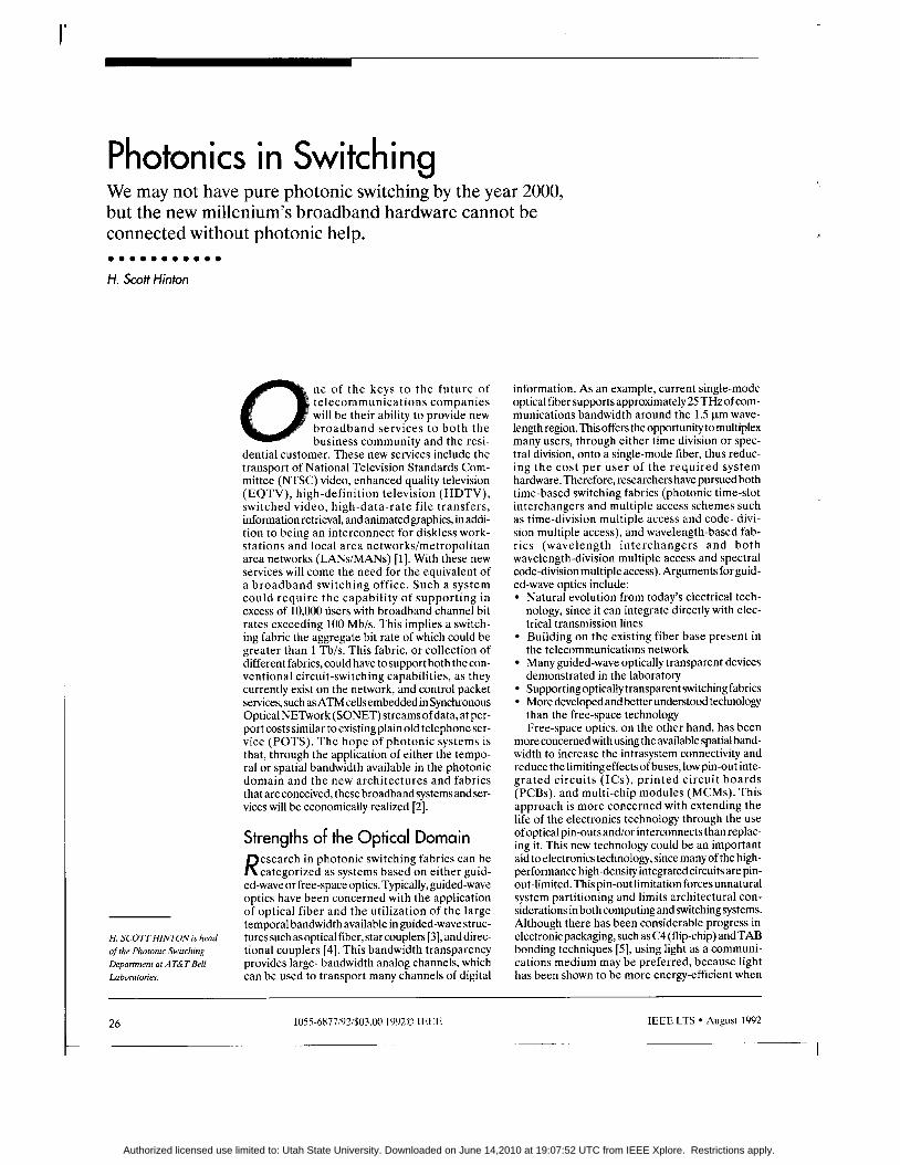
Space-Division Fabrics For over fifteen years, the mainstay of space-divi- sion guided-wave switching devices has been the directional coupler [12]. A directional coupler is a device that has two optical inputs, two optical ou tputs , and o n e cont ro l input , as shown in Fig. 1 . The control input is electrical and has the capability of put t ing t h e device in the bar o r bypass state-the upper (lower) optical inputs a re directed to the upper (lower) optical ou t - puts-or the cross (exchange) state-the upper (lower) optical inputs are directed to the lower ( u p p e r ) opt ical ou tputs . T h e most advanced implementations of these devices have occurred using t h e t i tanium-diffused l i thium niobate (Ti:LiNb03) technology, although there has been some effort in building these structures in the gallium arsenide (GaAs) and InPiInGaAsP mate- rial systems.
The strength of directional couplers is their optical transparency, which provides the ability to control extremely-high-bit-rate information. Their use is limited by several factors: the electronics required tocontrol them limits their maximum recon- figuration rate; the long length of each direction- al coupler prevents large-scale integration; and
l -
IEEE LTS August 1992
~. .
Authorized licensed use limited to: Utah State University. Downloaded on June 14,2010 at 19:07:52 UTC from IEEE Xplore. Restrictions apply.
. -7
: Frame : Frame : Frame Frame : Frame :
Figure 2. Universal time slots.
the losses and crosstalk associated with each device limit the maximum size of a possible network. unless some type of signal regeneration is includ- ed at critical points within the fabric.
Since directional couplers are 2 x 2 nonblock- ing switches, they can be linked together to create larger interconnection networks. For point-to-point networks, the interconnect ion of these 2 x 2 switching nodes can be accomplished using Clos. Benes, dilated Benes [ 131, banyan, omega, or shuffle network topologies [14]. As a result of thc analog nature of directional couplers, they are susceptible to crosstalk between channels and sig- nal loss. These noise and loss constraints limit the size of fabrics that can be built using these devices. To avoid the loss limitations, rearrangeably non- blocking networks such as Benes and di la ted Benes networks have been pursued because their
'i
Photonic time-slot interchanger
Input Time slot
output time slot
Connectivity diagram
Figure 3. Fiber-delay-line-based TSI.
total loss is logarithmically related to the size of the switch, O(logN), as opposed to crossbar net- works, the losses of which are linearly related to t h e size of t h e network, O ( N ) . T h e crosstalk problem, on the other hand, is reduced by choos- ing more robust networks, the control schemes of which do not allow both inputs of any 2 x 2 device to be active at any time. In these networks, one input will have active information present while the other inputwill contain only thecrosstalknoise from the previous stage. This is illustrated at the bot- tom o f Fig. 1, where the solid lines represent active signal lines and the dotted lines are crosstalk noise.Note that all thecouplersinanyactivatedpath have only one input active. Thus, as the informa- tion passes through adirectionalcoupler, onlyasec- ond-order crosstalk term can corrupt the desired output signal. Examples of such networks include dilated Benes, Ofman [ 151, and EGS networks [ 161. This implies that the analog-type problems asso- ciated with directional-coupler networks have been architecturally avoided to allow for the implementation of large switching fabrics. Unfor- tunately, the long length of directional couplers and the large bendingradii required in the integrated waveguides will limit the integration density of direc- tional couplers to small networks less than 32 x 32. These smaller networkswill then need to be inter- connected to create the larger-dimension fabrics required for the future.
A good application of direct ional-coupler- based fabrics is a protect ion switch for f iber transmission facilities. In this environment, the only time the switch will need to be reconfigured is when a failure occurs in an existing path. Thus, high bit rates can be passed through the switch with modera te reconfigurat ion-rate require- ments.
Ti me- Division Fabrics As a rcsult of the large signal bandwidth available in optically transparent devices, the signal bit rate passing through the device can be much largcr than the bit rate of any single user. I n this situa- tion, the information from the users can be com- pressed (in t ime) and share the t ransparent devices with many other users. There will be two types of time-division switching fabrics discussed in this section. T h e first two will be time-slot interchangers (TSIs), which actively rearrange the time slots in channelsof time- multiplexed infor- mation. The third time-division-based switchingfab- ric usesmultiple access techniques to use the available temporal bandwidth of a star coupler.
A conventional time-division multiplexed (TDM) signal is normally composed of either a bit-multi- plexed or block- multiplexed stream of information. A bit-multiplexed data stream is created by inter- leaving the compressed or sampled bit-synchronized bits from each of the users. This type of multi- plexing is the method of choice for most trans- mission systems, since it requires the storage of only one bit of information for each user at any time. Unfortunately, most of the bit-multiplexed trans- mission systems are further complicated by adding pulse-stuffing and other special control bits to the data stream. Block-multiplexing, on the other hand, stores a frame's worth of information from each of the users and then orders the bits entering the channel such that each user's data is contiguous.
28 IEEE LTS Auguct 1992
r ~
Authorized licensed use limited to: Utah State University. Downloaded on June 14,2010 at 19:07:52 UTC from IEEE Xplore. Restrictions apply.
When used in a switching environment, block multiplexing requires the switching fabric t o reconfigure only at block boundaries instead of bit boundaries, as in the case of bit-multiplexed data streams. By allowing a small amount of dead time between the block-multiplexed information, the requirements on the reconfiguration time of the fab- ric can b e relaxed. This can b e at t ract ive for switching devices such as directional couplers, which, when fabricated into large switching arrays, have slow to moderate reconfiguration times.
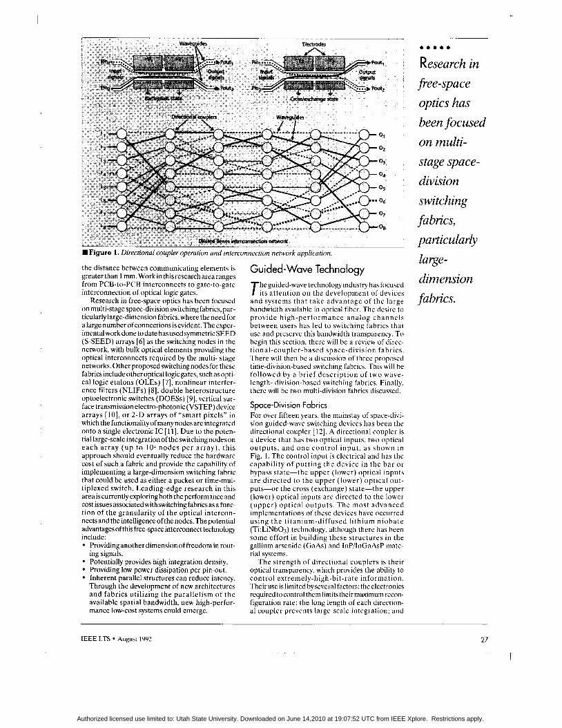
Agood application of the bandwidth transparency of optical1 fiber is through the use of universal time slots[l7]. A universal time slot is a parti- tioned section of time, which can contain infor- mation transmitted at any bit rate (see Fig. 2 ) . In this figure, a f rame is composed of 256 time slots. Each t ime s lot can conta in informat ion a t any bit ra te . For example, a time slot of voice would require approximately 100 kbis, while an adja- cent time slot could contain video information at a bit rate in excess of 1 Gbis.
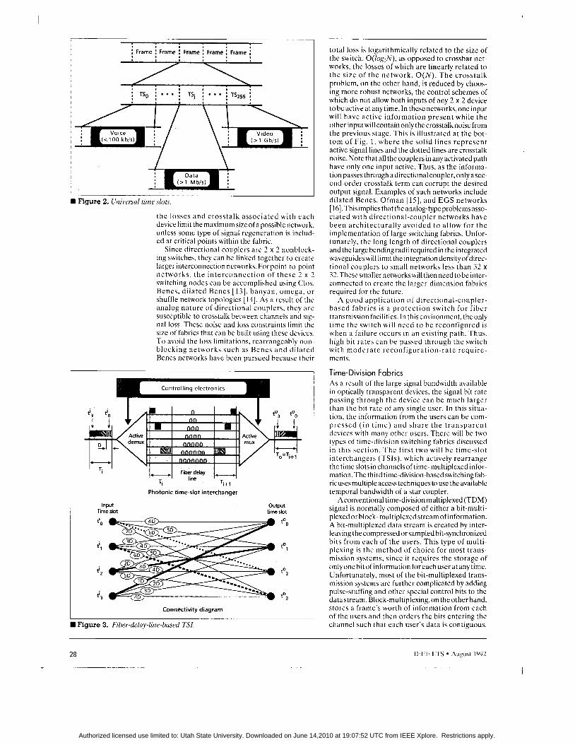
Time-Slot Interchangers-Switching can be achieved by interchanging the position, in time, of the time slots in a frame of time-multiplexed infor- mat ion. Most of the proposed photonic TSIs have been single-stage structures, in that the time slots of the input frame are directly mapped into the desired time slots of the output frame through the use of variable-length delay lines [18].
An example of such a TSI is shown in Fig. 3. In Fig. 3a, a time-multiplexed information stream with four time slots of duration Acomprise an input frame T,. The output frame TJb] leaving the TSI is delayed by one fIame delay (for this example, T = 4A) . T o perform the TSI function, each of the input time slots is directed to the appropriate number of time-slot delays to reposition it into the desired output frame time slot. By comparing the input frame, t:, to the output frame, t d , it can be seen that the following interchanging of time slots has to take place: t," + to?, t,' + t03, t ,2 + to ' , and t,.' -+ t,,O. The connectivity graph for this type of TSI is shown in Fig. 3b. This b ipar t i te graph representa t ion assigns the input and output time slots as the ver- tices (dots) and the edges as delays. The switch- ing between time slots is achieved by choosing the appropriate delay, which creates a virtual channel between an input and output time slot. As an example, for the information in ti' to be switched t o t , ,O, the delay line of 1 A must be used. T h e thick lines represent the connections shown in Fig. 3a. Since there is a path between any input time slot and any output time slot, this single- s tage network is fully connec ted . Also, since there are unique paths from each input time slot to each output time slot, the time-based network is also nonblocking.
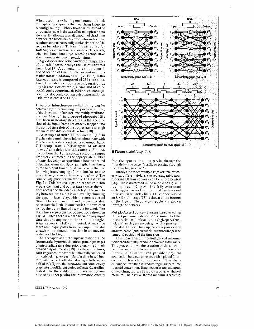
Another approach to the implementation of a TSI is to move the input time slots through multiple stages of intermediate time slots prior to arriving in their desired output time slot [19]. For these structures, eachstagedoes not have to be eitherfullyconnected or nonblocking. An example of a time-based but- terfly interconnect is illustrated in Fig. 4. In the upper half of this figure, the hardware and connectivity graphs for two different periods of butterfly are illus- t ra ted. T h e three different delays a r e accom- plished by either passing the information directly
Figure 4. Multi-stage TSI
from the input to the output, passing through the fiber delay line once ( N A/2), or passing through the delay line twice N A).
Through the use of multiple stagesof time switch- es with different delays, the rearrangeably non- blocking Ofman network can be implemented [20]. This is illustrated in the middle of Fig. 4. I t is composed of 210g2N - 1 serially connected exchangebypass nodes (directional couplers) and their associated delay lines. The connectivity of an 8 x 8 multi-stage TSI is shown at the bottom of t h e f igure. T h r e e active pa ths a r e shown through the network.
Multiple-Access Fabrics-The time-based switching fabrics previously descr ibed assume that the usersare time-multiplexedonto asingle spacechan- nel, with each user associated with a particular time slot. The switching operation is provided by an active reconfigurable fabric that interchanges the temporal position of the time slots.
Thus, rearranged time-multiplexed informa- tion is then demultiplexed and delivered to the users. This process allows the creation of virtual con- nections, in time, between users. Multiple-access fabrics, on the o ther hand, provide a physical connection between all users with a global inter- connect such as a bus or star coupler. This physi- cal connection is then shared among all users in time to avoid contention. Ring networks are examples of switching fabrics based on a passive shared medium. The passive shared medium is typically
IEEE LTS August 1992 29
I _ _ - ~ ~ ~~
Authorized licensed use limited to: Utah State University. Downloaded on June 14,2010 at 19:07:52 UTC from IEEE Xplore. Restrictions apply.
Coupler ' '
I tput
channels
input Sampling Coded Combined Bit Output bit clock input coded unputs pulse bit
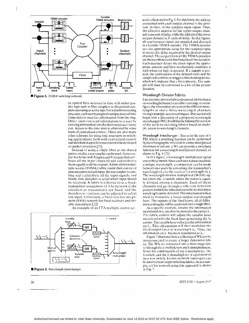
Figure 5. TDMA switching network.
an optical fiber accessed in time with either pas- sive taps such as fiber couplers or directional cou- plers operating as active taps. For a synchronous ring structure, each user is assigned a unique piece of time (time slot) to read the information from the ring. Other users can send information to a user by enteringinformation into the destination user's time slot. Access to the time slots is arbitrated by some form of centralized control. There are also many other schemes for using ring structures in switch- ing applications. both with centralized control and distributed asynchronous control schemes based o n packet structures [21].
Instead of using a single fiber as the shared passive media, astar coupler can be used. Astarcou- pler isadevicewithNinputs and Noutputs that com- bines all the input channels and redistributes them equally to all the outputs. A time-division mul- tiple access (TDMA) fabric could then consist of time encoderson each input, the star coupler to com- bine and redistribute all the input signals. and finally, time decoders t o select which input should be received. A fabric is referred to as a fixed- t ransmit ter assignment ( F T A ) network i f the encoders o r t ransmi t te rs a r e fixed, and the decoders or receivers can be adjusted to select any input. Conversely, a fixed-receiver assign- ment (FRA) network has fixed receivers and tun- able transmitters [22] .
An example of an FTA multiple-access net-
Tunable /- Switch laser ~ ,
~
Coherent / Laser detection \
... In I
1 " - " ' Laser ' 2 iaser
I , I, ... I"
mgth lexer 1
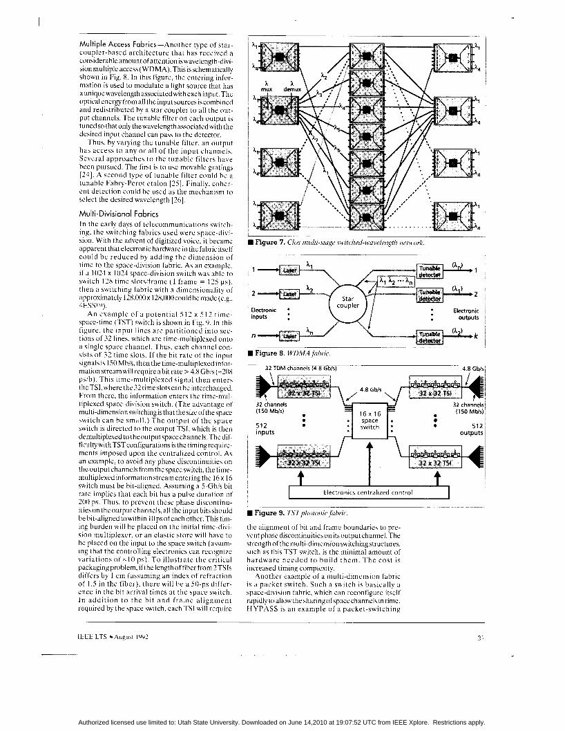
Figure 6. Wavelength interchanger,
work is illustrated in Fig. 5. For this fabric, the address associated with each output channel is the posi- tion, in time, of the sampled input signal. Thus, the effective address for the upper output chan- nel isone unit ofdelay,while theaddressofthelower output channel is N units of delay. In this figure, all synchronous inputs are sampled and directed to a tunable TDMA encoder. The TDMA encoder sets the appropriate delay for the sampled input to match the delay required by the desired output channel. The outputs from all the TDMA encoders are then combined and distributed to all the decoders. Each decoder delays the clock signal the appro- priate amount and then incoherently combines it with whatever light is present. If a sample is pre- sent, the combination of the delayed clock and the sample will combine to trigger a thresholdingdevice. which will indicate that a bit is present. The sam- ple will then be converted to a bit of the proper duration.
Wavelength-Division Fabrics Like the time-division fabrics discussed. fabrics based on wavelength channelscan either rearrange or recon- figure the information present on the different wave- lengths o r share those wavelength channels through multiple-access techniques. This section will begin with a discussion of a proposed wavelength interchanger(W1). Itwill then be followed by areview of the work on switching fabrics based on multi- plc access to wavelength channels.
Wavelength Interchanger-Just as in the case of a TSI, where a switching function can be performed by interchanging the time slots in a time-multiplexed information stream. a W1 can provide a switching function for a wavelength-multiplexed channel, as shown in Fig. 6 [23].
In this figure, a wavelength-multiplexed signal enters the p-switch. Since each user is associated with a unique wavelength. a connection can be made between two uscrs by converting the transmitter's wavelength (h , ) to the receiver's wavelength (hr). The wavelength-division multiplexed (WDM) sig- nal enters the h-switch. where the power is cqual- ly divided among n channels . Each of these channels will go through a coherent detection process in which the information on the desired input wavelength can be detected. This information is then used to modula te a f ixed-output wavelength laser. The outputs of the fixed lasers, all of differ- entwavelengths.wil1 bccombinedonto asingle fiber.
As a specific example, assume the information modulated on h, needs to be movcd to the carrier h,. The fabric control will adjust the tunable laser associated with the fixed laser generating the hi carrier. This tunable lascrwill select the information o n h,. This information will then modulate the fixed output laser of wavelength h, . Thus, the information on h,, has bccn transferred to h,.
Figure 7illustrates howacollectionofWIscan be interconnected to create a larger-dimension fab- ric. The Wls are connected into a three-stage fab- ric through the h-multiplexers and h-demultiplexers. Since the combination of the h-multiplexer, the A-switch, and the h-demultiplexer is equivalent to an 17 x 117 switch, known network topologies can be used tocreatr larger switchingfabrics. As an exam- ple, a Clos network using this approach is shown in Fig. 7.
Authorized licensed use limited to: Utah State University. Downloaded on June 14,2010 at 19:07:52 UTC from IEEE Xplore. Restrictions apply.
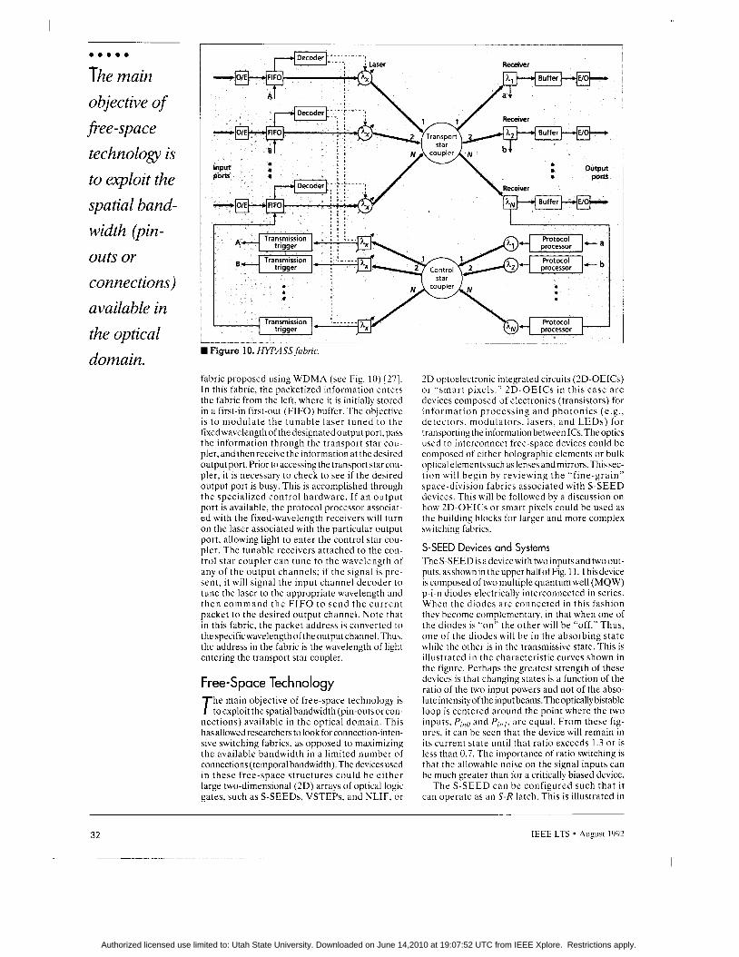
Multiple Access Fabrics-Another type of star- coupler-based architecture that has received a considerable amount of attention iswavelength-divi- sion multiple access (WDMA). This is schematically shown in Fig. 8. In this figure, the entering infor- mation is used to modulate a light source that has auniquewavelength associatedwith each input. The optical energy from all the input sources is combined and redistributed by a star coupler to all the out- put channels. The tunable filter on each output is tuned so that only the wavelength associatedwith the desired input channel can pass to the detector.
Thus, by varying the tunable filter. an output has access to any or all of the input channels. Several approaches t o the tunable filters have been pursued. The first is to use movable gratings [24]. A second type of tunable filter could be a tunable Fabry-Perot etalon [ 2 5 ] . Finally. coher- ent detection could be used as the mechanism to select the desired wavelength [26].
I
Multi-Divisional Fabrics
Electronics centralized control
In the early days of telecommunications switch- ing, the switching fabrics used were space-divi- sion. With the advent of digitized voice. i t became apparent that electronic hardware in the fabric itself could be reduced by adding the dimension of time to thc space-division fabric. As an example. i f a 1024 x 1024 space-division switch was able to switch 128 timc slotsiframe ( 1 frame = 125 ps), then a switching fabric with a dimensionality of approximately 128,000~ 128,000couldbe made (e.g., 4ESS’ ‘1).
An example of a potent ia l 512 x 512 t ime- space-time (TST) switch is shown in Fig. 9. In this figure, the input lines are partitioned into sec- tions of 32 lines, which are time-multiplexed onto a single space channel. Thus, each channel con- sists of 32 time slots. If the bit rate of the input signals is 150 Mbis. then the time-multiplexed infor- mation streamwillrequireabit rate > 4.XGb/s(=208 psib). This time-multiplexed signal then enters the TSI, where the 32 time slotscan be interchanged. From there, the information enters the time-mul- tiplexed spacc-division switch. (The advantage of multi-dimension switchingis that the size of the space switch can be small.) T h e output of the space switch is directed to the output TSI, which is then demultiplexed to the output space channels. The dif- ficultywith TSTconfigurations is the timing require- ments imposed upon the centralized control. As an example, to avoid any phase discontinuities on the outputchannelsfrom the space switch, the time- multiplexed informationstream enteringthe 16x 16 switch must be bit-aligned. Assuming a 5-Gbis bit rate implies that each bit has a pulse duration of 200 ps. Thus, to prevent these phase discontinu- itieson the output channels, all the input bitsshould he bit-aligned towithin 10psofeachother.This tim- ing burden will be placed on the initial time-divi- sion multiplexer, or an elastic store will have to be placed on the input to the space switch (assum- ing that the controlling electronics can recognize variations of =10 ps). T o illustrate t he critical packagingproblem, if the length of fiber from 2TSIs differs by 1 cm (assuming an index of refraction of 1.5 in the fiber), there will be a 50-ps differ- ence in the bit arrival times at the space switch. I n addi t ion t o t h e bit a n d fra.ne al ignment required by the space switch, each TSI will require
W Figure 7. CIOJ m Iti-stage J witched- wa t,elength network.
W Figure 8. WDMA fabric
4 8 Gblsi 32 TDM channels (4 8 Gbls)
32 channels! (1 50 Mb/s)
I 32 channels ~ (150 Mbls) . .
e e e 512 ~
outputs I 512 inputs
~ t 4 4
W Figure 9. TSTphotonic fuhric.
the alignment of bit and frame boundaries to pre- vent phase discontinuitieson itsoutputchannel.The strength of the multi-dimension switching structures, such as this TST switch, is the minimal amount of ha rdware needed t o build them. T h e cost is increased timing complexity.
Another example of a multi-dimension fabric is a packet switch. Such a switch is basically a space-division fabric, which can reconfigure itself rapidly to allow the sharing of space channels in time. HYPASS is an example of a packet-switching
IEEE LTS Auguq l Y Y 1
1-
-
31
Authorized licensed use limited to: Utah State University. Downloaded on June 14,2010 at 19:07:52 UTC from IEEE Xplore. Restrictions apply.
..... The main objective of free -space technology is to exploit the spatial band- width (pin- outs or connections) available in the optical domain.
\dTal- processor
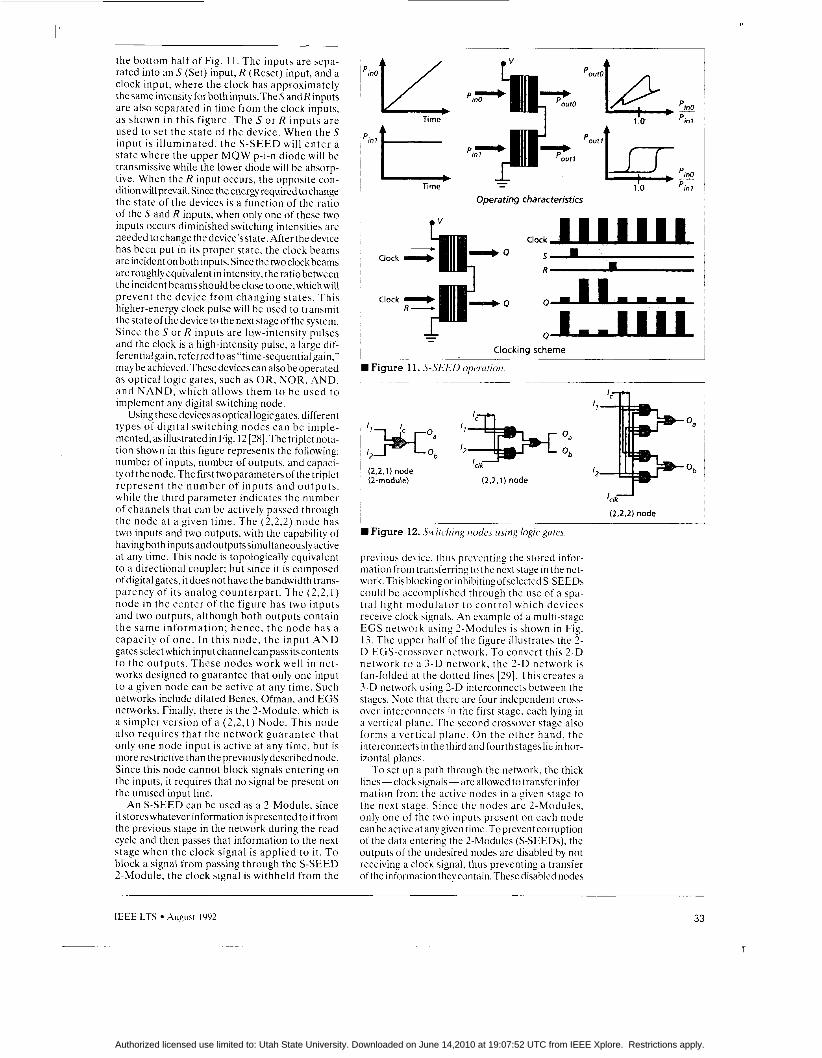
Figure 10. HYPASS fabric.
fabric proposed using WDMA (see Fig. 10) [27]. In this fabric, the packetized information enters the fabric from the left, where it is initially stored in a first-in first-out (FIFO) buffer. The objective is to modulate the tunable laser tuned to the fixed wavelength of the designated output port, pass the information through the transport star cou- pler, and then receive the information at the desired output port. Prior to accessing the transport star cou- pler, it is necessary to check to see if the desired output port is busy. This is accomplished through the specialized control hardware. If an output port is available, the protocol processor associat- ed with the fixed-wavelength receivers will turn on the laser associated with the particular output port, allowing light to enter the control star cou- pler. The tunable receivers attached to the con- trol star coupler can tune to the wavelength of any of the output channels; if the signal is prc- sent, it will signal the input channel decoder to tune the laser to the appropriate wavelength and then command t h e F I F O t o send the cur ren t packet to the desired output channel. Note that in this fabric, the packet address is converted to the specific wavelength of the output channel. Thus. the address in the fabric is the wavelength of light entering the transport star coupler.
Free-Space Tech nology he main objective of free-space technology is T to exploit the spatial bandwidth (pin-outsorcon-
nections) available in the optical domain. This has allowed researchers to look for connection-inten- sive switching fabrics. as opposed to maximizing the available bandwidth in a limited number of connections (temporal bandwidth). The devices used in these free-space s t ructures could be ei ther large two-dimensional (2D) arrays of optical logic gates, such as S-SEEDS, VSTEPs, and NLIF, or
2D optoelectronic integrated circuits (2D-OEICs) or “smart pixels.” 2D-OEICs in this case a r e devices composed of electronics (transistors) for information processing and photonics (e.g., detectors . modulators. lasers, and LEDs) for transporting the information between ICs. The optics used to interconnect free-space devices could be composed of either holographic elements or bulk optical elements such as lenses and mirrors. This sec- tion will begin by reviewing the “f ine-grain” s p ace -division fabrics associated with S - S E ED devices. This will be followed by a discussion on how 2D-OEICs or smart pixels could be used as the building blocks for larger and more complex switching fabrics.
S-SEED Devices and Systems The S-SEED isa device with two inputs and two out- puts,asshownin theupper halfofFig. 11.Thisdevice is composed of two multiple quantum well (MQW) p-i-n diodes electrically interconnected in series. When the diodes are connected in this fashion they become complementary, in that when one of the diodes is “on” the other will be “off.” Thus, one of the diodes will be in the absorbing state while the other is in the transmissive state. This is illustrated in the characteristic curves shown in the figure. Perhaps the greatest strength of these devices is that changing states is a function of the ratio of the two input powers and not of the abso- lute intensityof the input beams. The optically bistable loop is centered around the point where the two inputs, Pir10 and PIr l1 , are equal. From these fig- ures, it can be seen that the device will remain in its current state until that ratio exceeds 1.3 or is less than 0.7. The importance of ratio switching is that the allowable noise on the signal inputs can be much greater than for a critically biased device.
The S-SEED can be configured such that it can operate as an S-R latch. This is illustrated in
32 IEEE LTS August 1992
_ _ ~ - ~ _. r
Authorized licensed use limited to: Utah State University. Downloaded on June 14,2010 at 19:07:52 UTC from IEEE Xplore. Restrictions apply.
the bottom half of Fig. 11. The inputs are sepa- rated into an S (Set) input, R (Reset) input, and a clock input, where the clock has approximately the same intensity for both inputs.The S and R inputs are also separated in time from the clock inputs, as shown in this f igure. T h e S o r R inputs a r e used to set the s ta te of the device. When the S input is illuminated, the S-SEED will en te r a state where the upper MQW p-i-n diode will be transmissive while the lower diode will be absorp- tive. When the R input occurs, the opposite con- ditionwillprevail. Since theenergy required tochange the state of the devices is a function of the ratio of the S and R inputs, when only one of these two inputs occurs diminished switching intensities are needed tochange the device’sstate. After the device has been put in its proper state, the clock beams are incident on both inputs. Since the two clock beams are roughly equivalent in intensity, the ratio between the incidentbeamsshouldheclose toone,whichwill prevent the device from changing states. This higher-encrgy clock pulse will be used to transmit thestateofthcdevice to the nextstageofthesystem. Since the S or R inputs are low-intensity pulses and the clock is a high-intensity pulse, a large dif- ferential gain, referred to as “time-sequential gain.’. may be achieved. These devicescan also be operated as optical logic gates, such as OR, NOR. AND, and NAND, which allows them t o be uscd to implement any digital switching node.
Using these devicesasoptical logicgates, different types of digital switching nodes can be imple- mented,asillustratedin Fig. 12 [28].The triplet nota- tion shown in this figure represents the following: number of inputs, number of outputs, and capaci- tyofthe node. The first two parameter softhe triplet represent the number of inputs and outputs . while the third parameter indicates the number of channels that can be actively passed through the node at a given time. The (2,2,2) node has two inputs and two outputs, with thc capability of having both inputs and outputs simultaneously active at any time. This node is topologically equivalent to a directional coupler; but since it is composed ofdigitalgates,it doesnot have the bandwidth trans- parency of its analog counterpar t . Thc (2,2,1) node in the center of the figure has two inputs and two outputs, although both outputs contain the same information; hence, the node has a capacity of one . In this node , the input A N D gatessclectwhich input channelcan passitscontents to the outputs . These nodes work well in nct- works designed to guarantee that only one input to a given node can be active at any time. Such networks include dilated Benes, Ofman, and EGS networks. Finally, there is the 2-Module, which is a simpler version of a (2,2,1) Node. This node also requires that the network guarantee that only one node input is active at any time, but is more restrictive than the previously described node. Since this node cannot block signals entering on the inputs, it rcquires that no signal be present on the unused input line.
An S-SEED can be used as a 2-Module, since i t storeswhatever information is presented to it from the previous stage in the network during the read cycle and then passes that information to the next stage when the clock signal is applied to it. T o block a signal from passing through the S-SEED 2-Module, the clock signal is withheld from the
Operating characteristics
Clock
Clock a s. R.
I Clocking scheme
W Figure 1 1. S-SEED operatiom
‘ I
‘ I 0.3 0.3
Ob ‘2 Ob
‘2 Ob (2-module) (2,2,1) node
‘clk
, (2.2.2) node
W Figure 12. Sizitchirzg riocle.s ltsirig logic gutes.
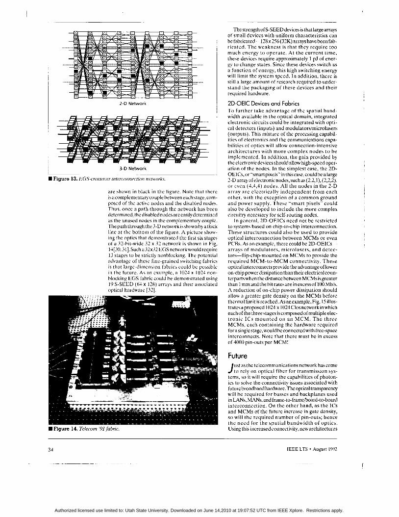
previous de\ ice. thus preventing the stored infor- mation from transferring to the next 5tage in the nct- work. This blocking or inhibiting ofselected S-SEEDS could be accomplished through the use of a spa- tial light modula tor to control which devices receive clock signals. An example of a multi-stage EGS network using 2-Modules is shown in Fig. 13. The upper half of the figure illustrates the 2- D EGS-crossover network. To convert this 2-D network to a 3 - D network, the 2-D network is fan-folded at the dotted lines [29]. This creates a 3-D network using 2-D interconnects bctween the stages. Note that there are four independent cross- over interconnects in the first stage, each lying in a vertical plane. The second crossover stage also forms a vertical plane. O n the other hand, the interconnects in the third and fourth stages lie in hor- izontal planes.
T o set up a path through the network. the thick lines-clock signals - are allowed to transfer infor- mation from the activc nodes in a given stage to the next stage. Since the nodes are 2-Modules, only one of the two inputs present on each node can be active at any given time. Toprevent corruption of the data entering the 2-Modules (S-SEEDS). the outputs of the undesired nodes are disabled by not receiving a clock signal, thus preventing a transfer of the information they contain. These disabled nodes
IEEE LTS August 1YOZ
Authorized licensed use limited to: Utah State University. Downloaded on June 14,2010 at 19:07:52 UTC from IEEE Xplore. Restrictions apply.
..... ....
..... ....
..... .....
2-D Network
3-D Network ~
W Figure 13. EGS-crossover interconnection networks.
arc shown in black in the figure. Note that there isacomplementarycouple between each stage,com- posed of the active nodes and the disabled nodes. Thus, once a path through the network has been determined, the disabled nodes are easily determined as the unused nodes in the complementary couple. Thepath through thc3-Dnetworkisshownbyathick line at the bottom of the figure. A picture show- ing the optics that demonstrated the first six stages of a 32-bit-wide 32 x 32 network is shown in Fig. 14[30,31].Sucha32~32EGSnetworkwouldrequire 13 stages to be strictly nonblocking. The potential advantage of these fine-grained switching fabrics is that large-dimension fabrics could be possible in the future. As an example, a 1024 x 1024 non- blocking EGS fabric could be demonstrated using 19 S-SEED (64 x 128) arrays and their associated optical hardware [32].
Figure 14. Telecom ‘91 fabric.
The strength of S-SEED devices is that large arrays of small devices with uniform characteristics can befabricated-128x 256(32K) arrays havebeenfab- ricated. The weakness is that they require too much energy t o opera te . A t t h e current time, these devices require approximately 1 pJ of ener- gy to change states. Since these devices switch as a function of energy, this high switching energy will limit the system speed. In addition, there is still a large amount of research required to under- stand the packaging of these devices and their required hardware.
2D-OEIC Devices and Fabrics To further take advantage of the spatial band- width available in the optical domain, integrated electronic circuits could be integrated with opti- cal detectors (inputs) and modulators/microlasers (outputs). This mixture of the processing capabil- ities of electronics and the communications capa- bilities of optics will allow connection-intensive archi tectures with more complex nodes t o be implemented. In addition, the gain provided by the electronic devices should allow high-speed oper- ation of the nodes. In the simplest case, the 2D- OEICs, or “smart pixels” in this case, could be a large 2-D array of electronicnodes, such as (2,2,1), (2,2,2), or even (4,4,4) nodes. All the nodes in the 2-D array a r e electrically independent f rom each other, with the exception of a common ground and power supply. These “smart pixels” could also be developed to include the more complex circuitry necessary for self-routing nodes.
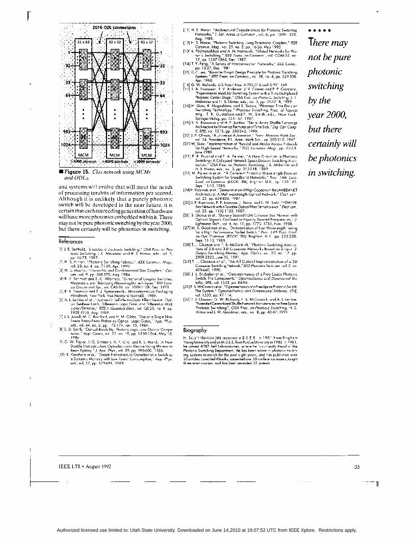
In general, 2D-OEICs need not be restricted to systems based on chip-to-chip interconnection. These structures could also be used t o provide optical interconnection between MCMs or even PCBs. As an example, there could be 2D-OEICs- arrays of modulators, microlasers, and detec- tors-flip-chip-mounted on MCMs to provide the required MCM-to-MCM connectivity. These optical interconnectsprovide the advantage of lower on-chip power dissipation than their electrical coun- terparts when the distance between MCMs isgreater than 1 mmandthebitratesareinexcessof 100Mb/s. A reduction of on-chip power dissipation should allow a greater gate density on the MCMs before thermal limit is reached. As an example, Fig. 15 illus- tratesaproposed 1024 x 1024Closnetworkinwhich each of the three stages is composed of multiple elec- t ron ic ICs m o u n t e d on a n MCM. T h e t h r e e MCMs, each containing the hardware required for a single stage, would be connected with free-space interconnects. Note that there must be in excess of 4000 pin-outs per MCM!
Future ust as the telecommunications network has come j t o rely on optical fiber for transmission sys-
terns, so it will require the capabilities of photon- ics to solve the connectivity issues associated with future broadband hardware. The optical transparency will be required for busses and backplanes used in LANs, MANS, and frame-to-frameboard-to-board interconnection. O n the other hand, as the ICs and MCMs of the future increase in gate density, so will the required number of pin-outs; hence the need for t h e spat ia l bandwidth of optics. Using this increased connectivity, new architectures
Authorized licensed use limited to: Utah State University. Downloaded on June 14,2010 at 19:07:52 UTC from IEEE Xplore. Restrictions apply.
I'
I Figure 15. Clos network using MCMs and ODLs.
and systems will evolve that will meet the needs of processing terabits of information per second. Although it is unlikely that a purely photonic switch will be developed in the near future, it is certain that each succeedinggeneration of hardware will have more photonics embeddedwithin it. There may not be pure photonicswitching by theyear 2000, but there certainly will be photonics in switching.
References [ I ] J E. Berthold, "Broadband Electronic Switching," OSA Proc on Pho-
tonic Switching, J E. Midwinter and H S Hinton, eds , vol 3, pp 66-73, 1989.
[2] H. S . Hinton, "Photonic Switching Fabrics,", IEEE Commun M a g , vol 28. no 4. oa 71-89. Aar 1990.
[3] M. E Marhic, "Hierarchic and Combinatorial Star Couplers," Opt
141 R . V. Schmidt and R. C Alferness. "Dlrectlonal Coualer Switches Lett, vol 9, pp 368.370. Aug 1984.
. , Modulators, and Filters Using Alternating DbTechniques," IEEE Trans' on Circuits and Sys., vol. CAS-26, pp 1099-1 108, Dec 1979
[5] R R Tummala and E. J. Rymaszewski, Microelectronics Packaging Handbook, New York: Van Nostrand Reinhold, 1989.
[6] A L Lentine et 01.. "Symmetric Self-Electro-optic Effect Devlce Opti- cal Set-Reset Latch, Differential Logic Gate, and Differential Mod- ulator/Detector," IEEEJ Quantum Elect, vol QE-25, no 8, pp. 1928-1 936, Aug. 1989
171 J 1. Jewell. M. C. Rushford. and H. M Gibbs. "Use of a Sinale Non- . . linear Fabry-Perot Etolon as Optical Log'ic Gates," A& Phys Lett., vol. 44, no. 2. pp 172.174. Jon 15, 1984
181 S. D Smith, "Oatlcal Bistabilitv. Photonic Loaic. and Ootical Comou- . I tation," A& optics, v01 25, no I O , p i i 5 5 0 - 1 h t . ay i s , 1986.
191 G W . Taylor, J G Simmons, A. Y. Cho. and R. S Mand, "A New Double Hetrostructure Optoelectronic Device Using Molecular Beam Epitaxy," J. App Phys.. vol 59, pp. 596-600, 1986.
[ I O ] K. Kasohara et 0 1 , "Double Hetrostructure Optoelectronic Switch as a Dynamic Memory with Low Power Consumption," App Phys Len., vol. 52, pp 679.681. 1988
[ l I ] H. S. Hinton, "Architectural Considerations for Photonic Switching Networks,"J. Sel. Areas in Commun., vol. 6, p p 1209-1 226, Aug. 1988.
(1 21 H. S. Hinton, "Photonic Switching Using Directional Couplers," IEEE Commun. Mag., vol. 25 , no. 5, pp. 16-26. May 1985.
[13] K Padmanabhan and A N. Netravali, "Dilated Networks for Pho- tonic Switching," IEEE Trans. on Commun , vol COM-35, no 12, pp. 1357.1 365, Dec. 1987.
[I41 T:Y. Feng, "A Survey of Interconnection Networks," IEEE Comp , pp. 12-27, Dec. 198 1 .
[IS] C:T. Leo, "Bipartite Graph Design Principle for Photonic Switching Systems," IEEE Trans. on Commun, vol 38, no 4, pp. 529.538. Apr. 1990.
[16] G. W. Richards, U.S Patent Nos. 4,993,016and 4,991,168. [ 171 R. A. Thompson. R. V. Anderson, J. V. Camlet, and P P Giordano,
"Experimental Modular Switching System with a Time-Multiplexed Photonic Center Stage," OSA Proc. on Photonic Switching, J E. Midwinter ond H. S. Hinton, eds., vol. 3, pp. 212.218. 1989.
[ l 81 H Gato, K Nagashima. and S. Suzuki, "Photonic Time-Division Switching Technology," Photonic Switching: Proc 1st Topical M t g . , T . K. Gustafson a n d P . W . Smith, eds , N e w York Springer-Verlag, pp. 151-157, 1987
[19] S. V. Ramanan and H. F Jordon, "Serial Array Shuffle-Exchange Architecture for Universol Permutation ofTime-Slots," Dig Opt Comp. If, SPIE, vol. 1215, pp. 330342, 1990
[ZO] J. P. Ofman, "A Universal Automation." Trons Moscow Math SOC , vol. 14, Providence, R.I.. Amer. Math Soc., pp 2002 15, I967
[21] M. Skov, "Implementation of Physical and Media Access Protocols for High-speed Networks." IEEE Commun M a g , p p 45-53, June 1989.
[22] P. R. Prucnal and P. A. Perrier, "A N e w Direction i n Photonic Switching: A Collapsed-Network SpoceDivision Switching Archi tecture," OSA Proc on Photonic Switching, J. E Midwinter and H. S. Hinton, eds.. vol 3, pp. 2 12-2 18, 1989.
[23] M. Fijiwara et 01 , "A Coherent Photonic Wavelength-Division Switching System for Broadband Networks," Proc 14th Euro Conf. on Commun. (ECOC '881. Brighton, U K , pp 139 142, Sept 11-15. 1988.
[24] H Kobrinskietal.."DemonstrationofHighCapacityin thelAMBDANET Architecture. A Multiwavelength Optical Network," Elect Lett vol. 23. pp. 824-826, 1987
[25] I. P Kaminow, P. P Iannone, J. Stone, and L W Stulz, "FDM-FSK StorNetwarkwithaTunableOptical Filter Demultiplexor," Elect Len, vol 23. pp. 1102-1 103, 1987.
[26] 8. Glance et al., "Densely Spaced FDM Coherent Star Network with Optical Signals Confined to Equally Spaced Frequencies," J lighhvave Tech.. vol. 6, no. I I , pp. 1770- 1781, Nov I988
[27] M S Goodman et al.. "Demonstration of Fast Wavelength Tuning for a High Performance Pocket Switch," Proc 14th Euro. Conf on Opt Commun ( K O C '88J. Brighton, U K , pp 255 258, Sept. 11-15, 1988.
[28] T. J. Cloonan ond F. B McCormick, "Photonic Switching Applica- tions of 2-D and 3-D Crossover Networks Based on 2~lnput. 2 Output Switching Nodes," App Optics, vol 30, no 17, p p 2309-2323, June IO, 1991
[29] T . J Cloonan et al., "An Al l -Opt ical Implementatdon of a 3D Crossover Switching Nehvork,"lEEEPhotonics Tech Len , vol. 2, pp 438-440, 1990.
[30] J L Bruboker et al.. "Optomechanics of a Free-Spoce Photonic Switch: The Components," Optomechanics ond Dimensronal Sta- bility, SPIE, vol. 1533. pp 88-96
[3 I ] F. B.McCormicketa1.. "Optomechanicsofa Freespace PhotonicSwitch The System," Optomechanicr and Dimensional Stability, SPIE, vol. 1533, pp. 97-1 14.
[32] T J Cloonan, G. W Richards, F. B. McCormick, and A L Lentine, "Extended Generalized Shuffle Network Architectures for Free-Space Photonic Switching", OSA Proc on Photonic Switching, H. S Hinton and J. W . Goodman, eds , vol 8, pp 43-47, 1991
..... There may not be pure photonic switching by the year 2000, but there certainly will be photonics in switching.
Biography H. SCOTT HINTON (M) received a B.S E E in 1981 from Brigham Young UniversityandanM S.E.E from PurdueUniversityin I982 In 1981, he ioined ATBT Bell Laboratories, where he i s currently Head of the Photonic Switching Department. He has been active in photonic switch- ing systems research for the post eight years, and has published over 20articles. coedited4 books, presentedover 5Oconference papers, taught three short courses, and has been owarded 12 patents.
IEEE LTS August 1YY2 35
Authorized licensed use limited to: Utah State University. Downloaded on June 14,2010 at 19:07:52 UTC from IEEE Xplore. Restrictions apply.