phonon engineering in nanodimensional structures
TRANSCRIPT

MOLDOVA STATE UNIVERSITY
With the rights of manuscript UDC: 539.21
NICA DENIS
PHONON ENGINEERING IN NANODIMENSIONAL STRUCTURES
131.04 - COMPUTATIONAL PHYSICS AND MODELING OF PROCESSES
Scientific Review of the habilitate doctor thesis in physics based on published articles
CHISINAU, 2016

2
The Thesis has been elaborated in the Scientific Research Laboratory “Physics and engineering of nanomaterials E. Pokatilov” at the Moldova State University.
Scientific consultant: BALANDIN Alexander PhD, professor, University of California ‒ Riverside, U.S.A.
Official referees: CASIAN Anatolie habilitate doctor in physics and mathematics, professor, Technical
University of Moldova; BELOUSOV Igor habilitate doctor in physics and mathematics, professor, Institute of
Applied Physics of the Academy of Sciences of Moldova; KHITUN Alexander PhD, professor, University of California ‒ Riverside, U.S.A.
Members of the Specialized Scientific Council: HADJI Piotr Chairman, habilitate doctor in physics and mathematics, professor,
Institute of Applied Physics of the Academy of Sciences of Moldova; TRONCIU Vasile Scientific Secretary, habilitate doctor in physics and mathematics,
associate professor, Technical University of Moldova; CANȚER Valeriu habilitate doctor in physics and mathematics, academician of the
Academy of Sciences of Moldova, professor, D. Ghitu Institute of Electronic Engineering and Nanotechnologies of the Academy of Sciences of Moldova;
PALADI Florentin habilitate doctor in physics and mathematics, associate professor, Moldova State University;
MACOVEI Mihai habilitate doctor in physics and mathematics, associate professor, Institute of Applied Physics of the Academy of Sciences of Moldova;
BARSUC Alexandru habilitate doctor in physics and mathematics, professor, Moldova State University;
NICOLAEVA Albina habilitate doctor in physics and mathematics, professor, D. Ghitu Institute of Electronic Engineering and Nanotechnologies of the Academy of Sciences of Moldova.
The defense of the Thesis will be held on May 20, 2016 at 16:00 on the session of the Specialized Scientific Council DH 30.131.04-02 of the Moldova State University (A. Mateevici str. 60, bl. 4, aud. 222, Chisinau, MD-2009, Moldova).
The Scientific Review can be consulted at the Library of the Moldova State University (A. Mateevici str. 60, Chisinau, MD-2009, Moldova) and on the webpage of the National Council for Accreditation and Attestation (www.cnaa.md).
The Scientific Review was distributed on April 15, 2016. Scientific Secretary of the Specialized Scientific Council, TRONCIU Vasile, habilitate doctor, associate professor ___________
signature
Scientific Consultant, BALANDIN Alexander, PhD, professor ___________
signature
Author, NICA Denis ___________
signature
© Nica Denis, 2016

3
TABLE OF CONTENTS
SUMMARY (ENGLISH, ROMANIAN, RUSSIAN) ................................................................. 5
LIST OF ABBREVIATIONS ....................................................................................................... 8
INTRODUCTION ......................................................................................................................... 9
1. PHONON ENGINEERING AT NANOSCALE ................................................................... 13
1.1. Phonons and thermal transport in semiconductor nanostructures ...................................... 13
1.2. Phonons and thermal transport in graphene materials ........................................................ 16
1.3. Conclusions to Chapter 1 .................................................................................................... 22
2. PHONON ENGINEERING IN TWO-DIMENSIONAL SEMICONDUCTOR
NANOSTRUCTURES ................................................................................................................ 24
2.1. Engineering of phonon energy spectra and group velocities in two-dimensional
semiconductor nanostructures ................................................................................................... 24
2.1.1. Continuum model for phonons in two-dimensional nanostructures ............................ 24
2.1.2. Dynamic models of lattice vibrations in two-dimensional nanostructures with
diamond-like crystal lattice ................................................................................................... 29
2.2. Phonon engineered thermal conductivity in multilayered nanostructures
with core Si layer ....................................................................................................................... 33
2.3. Phonon engineered enhancement of electron mobility in two-dimensional
heterostructures with Si and GaN conduction channels ............................................................ 36
2.4. Conclusions to Chapter 2 .................................................................................................... 39
3. PHONON ENGINEERING IN ONE-DIMENSIONAL SEMICONDUCTOR
NANOSTRUCTURES ................................................................................................................ 41
3.1.Engineering of phonon energy spectra and group velocities in GaN and Si nanowires
with elastically dissimilar cladding layers ................................................................................. 41
3.1.1. Continuum model for phonons in rectangular and cylindrical
GaN-based nanowires ............................................................................................................ 41
3.1.2. Dynamic models of lattice vibrations for nanowires with diamond-like
crystal lattice .......................................................................................................................... 45
3.2. Phonon engineered thermal conductivity in Si-based nanowires. ...................................... 47
3.3. Conclusions to Chapter 3 .................................................................................................... 50

4
4. PHONON ENGINEERING IN GRAPHENE ....................................................................... 51
4.1. Phonons in graphene ........................................................................................................... 51
4.2. Lattice thermal conductivity in graphene ........................................................................... 55
4.3. Lattice thermal conductivity in graphene ribbons .............................................................. 61
4.4. Conclusions to Chapter 4 .................................................................................................... 64
GENERAL CONCLUSIONS AND RECOMMENDATIONS ............................................... 65
REFERENCES ............................................................................................................................ 67
RESPONSIBILITY DECLARATION ...................................................................................... 80
CURRICULUM VITAE ............................................................................................................. 81

5
SUMMARY (ENGLISH, ROMANIAN, RUSSIAN)
Nica Denis, “Phonon engineering in nanodimensional structures”, scientific review of the
habilitae doctor thesis in physics (based on published articles), Chisinau, 2016. Introduction, 4
Chapters, General conclusions and recommendations, 176 references, 91 pages, 25 figures, 2
tables. Based on the obtained results, 150 scientific works were published, including one
monograph, two books chapters, 6 review papers and 33 research articles in ISI journals, 12
articles in national scientific journals and over 100 abstracts in proceedings/books of abstracts of
international or national conferences.
Keywords: phonons, electrons, thermal transport, semiconductor nanostructures, nanofilm,
nanowire, graphene, phonon engineering, continuum approach, crystal lattice dynamics.
Domain of study: physics of nanosystems.
Goal and objectives: theoretical development of phonon engineering concept for one- and two-
dimensional multilayered semiconductor nanostructures and graphene for improvement of their
electrical and thermal conductivities.
Scientific novelty and originality: the theoretically developed phonon engineering concept for
multilayered semiconductor nanostructures and graphene is fundamentally new approach for
improvement of thermal and electrical properties of nanostructures by a proper tuning of their
phonon properties; the phonon states in considered nanostructures are investigated in detail,
using different models of crystal lattice vibrations; the developed theory of heat transport allows
interpretation of extremely high values of phonon thermal conductivity in graphene and its
strong dependence on spatial dimensions of graphene flakes, concentration of crystal lattice
defects and edge roughness.
Theoretical importance: accurate models of phonon transport in multilayered semiconductor
nanostructures and graphene are developed; the peculiarities of phonon processes in such
nanostructures are theoretically investigated and explained.
Practical significance of the obtained results is related to a possible improvement of operational
parameters of modern nanostructure-based devices by proper tuning of their phonon properties.

6
АDNOTARE
Nica Denis, „Ingineria fononică în structurile nanodimensionale”, referatul științific al tezei de
doctor habilitat în științe fizice (prezentată în baza lucrărilor științifice publicate), Chișinău,
2016. Introducere, 4 Capitole, Concluzii generale și recomandări, 176 titluri bibliografice, 91
pagini, 25 figuri, 2 tabele. În baza rezultatelor obținute au fost publicate 150 lucrări științifice,
inclusiv o monografie, 2 capitole în monografii, 6 articole de sinteză și 33 articole în revistele
cotate de ISI Web of Science, 12 articole în revistele științifice naționale și peste 100 teze la
conferințele internaționale și naționale.
Cuvinte-cheie: fononi, electroni, transport termic, nanostructuri semiconductoare, nanostrat,
nanofir, grafen, inginerie fononică, abordare continuală, dinamica rețelei cristaline.
Domeniul cercetărilor: fizica nanosistemelor.
Scopul și obiectivele: dezvoltarea teoretică a conceptului ingineriei fononice în nanostructurile
semiconductoare multistrat uni- și bidimensionale și în grafen pentru îmbunătățirea
conductibilității termice și electrice a lor.
Noutatea științifică și originalitatea: în lucrare este dezvoltată concepția de inginerie fononică
în nanostructurile semiconductoare și în grafen, care reprezintă o metodă principial nouă de
îmbunătățire a proprietăților termoconductibile și electroconductibile ale nanostructurilor prin
dirijarea direcționată a proprietăților fononice ale lor; în cadrul diferitor modele ale oscilațiilor
rețelei cristaline au fost cercetate detaliat stările fononice în nanostructurile studiate; a fost
dezvoltată teoria transportului de căldură, care explică valorile înalte ale conductibilității termice
de rețea a grafenului, cât și dependența puternică a ei de dimensiunile spațiale ale stratului, de
concentrația defectelor rețelei cristaline și de calitatea frontierelor stratului.
Importanța teoretică: au fost elaborate modele teoretice exacte ale transportului fononic în
nanostructurile semiconductoare multistrat și în grafen; au fost cercetate teoretic și explicate
particularitățile proceselor fononice în astfel de structuri.
Importanța aplicativă a rezultatelor obținute este legată de posibilitatea îmbunătățirii
caracteristicilor de lucru ale dispozitivelor electronice moderne prin modificarea proprietăților
fononice ale lor.

7
АННОТАЦИЯ
Ника Денис, „Фононная инженерия в наноразмерных структурах”, научный реферат
диссертации на соискание ученой степени доктора хабилитат физических наук (на основе
опубликованных научных работ), Кишинев, 2016. Введение, 4 Главы, Общие выводы и
рекомендации, 176 cсылок, 91 cтраница, 25 рисунков, 2 таблицы. На основе полученных
результатов опубликовано 150 научных работ, включая монографию, две главы в
монографии, 6 обзорных и 33 исследовательские статьи в международных журналах,
индексируемых ISI Web of Science, 12 статей в национальных научных журналах и более
100 тезисов на международных и национальных конференциях.
Ключевые слова: фононы, электроны, тепловой транспорт, полупроводниковые
наноструктуры, нанослой, нанонить, графен, фононная инженерия, континуальный
подход, динамика кристаллической решетки.
Область исследований: физика наносистем.
Цель и задачи: теоретическое развитие концепции фононной инженерии в одно- и
двумерных многослойных полупроводниковых наноструктурах и графене для улучшения
их теплопроводящих и электропроводящих свойств.
Научная новизна и оригинальность: в работе развита концепция фононной инженерии
в многослойных полупроводниковых наноструктурах и графене, которая представляет
собой принципиально новый метод улучшения теплопроводящих и электропроводящих
свойств наноструктур путем целенаправленного управления их фононными свойствами; в
рамках различных моделей колебаний кристаллической решетки детально исследованы
фононные состояния в рассматриваемых наноструктурах; развита теория теплового
транспорта, которая объясняет как высокие значения решеточной теплопроводности
графена, так и ее сильную зависимость от пространственных размеров слоя, концентрации
дефектов кристаллической решетки и качества границ слоя.
Теоретическая значимость: разработаны точные модели фононного транспорта в
многослойных полупроводниковых наноструктурах и графене; теоретически исследованы
и объяснены особенности фононных процессов в таких структурах.
Прикладная ценность полученных результатов связана с возможным улучшением
рабочих характеристик современных электронных устройств путем изменения их
фононных свойств.

8
LIST OF ABBREVIATIONS
RT – room temperature
1D – one-dimensional
2D – two-dimensional
3D – three-dimensional
MFP – mean free path
GNR – graphene nanoribbon
BvK model – Born-von Karman model
FCC model – face-centered cubic cell model
VFF model – valence force field model
MD – molecular dynamics
BTE – Boltzmann transport equation
IFC – interatomic force constant
SLG – single layer graphene
FLG – few layer graphene
NW – nanowire
SNW – segmented nanowire
MSNW – modulated segmented nanowire
– phonon group velocity
– Plank’s constant
Bk – Boltzmann’s constant
T – absolute temperature

9
INTRODUCTION
Relevance and importance of the Thesis. Phonons manifest themselves in all major processes in
semiconductors: they carry heat, limit electron mobility, affect optical response and transmit
sound. Reduction of the size of electronic devices below the acoustic phonon mean free path
creates a new situation for the phonons propagation and interaction. From one side, it may
complicate heat removal from the downscaled devices due to decrease of phonon group velocity
and enhancement of phonon boundary scattering. From the other side, it opens up an opportunity
for engineering phonon spectrum in nanostructured materials. Phonon engineering is an
approach to tune the phonon properties of materials for enhancement of their thermal and
electronic properties. This approach is fundamentally different from the conventional –
packaging level – heat removal techniques or electronic band-gap engineering. The practical
application of phonon engineering at nanoscale may lead to important advancement in micro-
and nanoelectronics and to appearance of a novel class of phonon-optimized nanostructured
materials and devices.
The goals of the Thesis are:
theoretical development of phonon engineering concept for one- and two-dimensional
multilayered semiconductor nanostructures and graphene;
demonstration of a possibility for phonon-engineered enhancement of their electrical and
thermal conductivities.
In order to achieve these goals, the following objectives are formulated:
Development of theoretical models for phonons and thermal transport in multilayered
semiconductor nanostructures and graphene;
Investigation of electron properties and electron-phonon interaction in planar
multilayered semiconductor nanostructures;
Investigation of phonon scatterings in multilayered semiconductor nanostructures and
graphene;
Optimization of nanostructures over shape and size to achieve optimal thermal
conductivity and increased electron mobility.
The following theoretical methods and models are used to accomplish the objectives:
Continuum approach and dynamic models of lattice vibrations for phonons;
Effective-mass approximation for electrons;
Boltzmann transport equation within relaxation time approximation for modeling the
thermal and electronic properties of considered nanostructures.

10
Finite difference method for numerical solving of systems of differential equations; QR
decomposition approach for numerical solving of eigenvalues/eigenvectors problems;
rectangle method for numerical integrations.
Theoretical importance and scientific novelty of the results consists in the following:
A continuum approach and three dynamic models of lattice vibrations: face-centered
cubic cell (FCC), Born-von Karman (BvK) and valence force field (VFF) were developed
and applied for the investigation of phonon properties of multilayered semiconductor
nanostructures and graphene;
A possibility of tuning the thermal and electrical conductivities in semiconductor
nanostructures and graphene by proper engineering of their phonon properties is
theoretically demonstrated;
A theoretical model of phonon thermal transport in graphene, few-layer graphene, twisted
graphene and graphite was developed and applied for the investigation of heat
conduction;
Theoretical interpretation of extremely high values of phonon thermal conductivity in
graphene materials and its strong dependence on lateral dimensions, thickness and shapes
of graphene flakes, edge roughness, point defects and isotope is provided.
The theoretically developed phonon engineering concept at nanoscale is fundamentally new
approach for improvement of thermal and electrical conduction in semiconductor nanostructures
and graphene.
The theoretical significance of the results consists in developing of accurate models for phonons
and thermal transport in multilayered semiconductor nanostructures and graphene; in
investigations of peculiarities of phonon processes at nanoscale and in demonstration of a
possibility to achieve phonon-engineered enhanced thermal or electrical properties of
multilayered semiconductor nanostructures and graphene.
The applied significance of the results is related to a possible improvement of operational
parameters of modern nanostructure-based devices by proper tuning of their phonon properties.
Main items to be defended:
1. Phonon energy spectra and group velocities in semiconductor planar heterostructures and
coated nanowires can be efficiently tuned by a proper selection of cladding layers material
and thickness.

11
2. Cladding layers with higher (lower) sound velocity than that in a core layer increases
(decreases) both average group velocity of phonons and thermal conductivity.
3. New types of hybrid phonon modes appear in planar heterostructures and coated nanowires:
(i) core-like modes with atomic vibrations in the core layer; (ii) cladding-like modes with
atomic vibrations in the cladding layers and (iii) propagating modes with atomic vibrations
both in the core and cladding layers.
4. A two- to fivefold increase of the room temperature electron mobility can be achieved in
wurtzite AlN/GaN/AlN heterostructures by the compensation of built-in electric field by the
external electric field or by creation in the middle of GaN well ultra-narrow InXGa1-XN
nanogroove with small In content x ~ 0.05.
5. The electron mobility in silicon nanolayers can be increased if they are embedded within
cladding layers with higher sound velocity.
6. The phonon thermal conductivity in semiconductor segmented nanowires and cross-section-
modulated nanowires can be decreased by an order of magnitude in comparison with that in
straight nanowire due to the phonon filtering, i.e. trapping of the certain phonon modes in
nanowire segments.
7. The in-plane lattice thermal conductivity of single layer graphene strongly depends on the
temperature, lattice anharmonicity, point defects concentration, edge roughness, shape and
linear dimensions of the graphene flake.
8. The in-plane lattice thermal conductivity in few-layer graphene decreases rapidly with
increasing number of graphene monolayers n and approaches the highly-oriented pyrolitic
graphite limit for n=4.
9. The in-plane thermal conductivity of micrometer size rectangular graphene ribbons
demonstrates non-monotonic dependence on flake size due to the long mean-free path of
long-wavelength acoustic phonons.
10. Twisting bilayer graphene leads to the emergence of hybrid folded phonons, which depend
on the twisting angle and originate from the mixing of phonon modes from different high-
symmetry directions in the Brillouin zone.
Approbation of the results: over 100 presentations at the international and national scientific
conferences were given in United States of America, Russia, Japan, Germany, Italy, Belorussia,
Ukraine, Poland, Greece, Turkey and Moldova, including 5 invited plenary talks and 19 regular
oral presentations, presented directly by the Thesis author.

12
Publications: based on the results presented in the Thesis 150 scientific works were published,
including one monograph, two books chapters, 6 review papers and 33 research articles in ISI
journals, 12 articles in national scientific journals and over 100 abstracts in proceedings/books of
abstracts of international or national conferences.
Structure of the Scientific Review: the Review consists of Introduction (General characteristic of
the work), 4 Chapters and Conclusions. It contains 176 References, 87 Pages, 25 Figures and 2
Tables.
Keywords: phonons, electrons, thermal transport, semiconductor nanostructures, nanofilm,
nanowire, graphene, phonon engineering, continuum approach, crystal lattice dynamics.

13
1. PHONON ENGINEERING AT NANOSCALE
Phonons, i.e. quanta of the crystal lattice vibrations, affect all physical processes in solids [1-
3]. They limit the electron mobility near room temperature (RT), and affect optical properties of
crystalline materials. Acoustic phonons are the main heat carriers in insulators and
semiconductors [1]. The long-wavelength phonons give rise to sound waves, which explains the
name phonon. Phonons are characterized by their dispersion (q), where is an angular
frequency and q is a wave vector of a phonon [1-3]. In bulk semiconductors with g atoms per
unit cell, there are 3g phonon dispersion branches for each q [2]. Three types of vibrations at
long wavelength limit describe the motion of the unit cell, and form three acoustic phonon
branches. The other 3(g-1) modes describe the relative motion of atoms inside a unit cell, and
form the optical phonon branches. The acoustic polarization branches are commonly referred to
as longitudinal acoustic (LA) and transverse acoustic (TA). In case of graphene the out-of-plane
transverse vibrations are denoted as z-axis acoustic (ZA) phonons [4-6]. In the long-wavelength
limit, acoustic phonons in bulk crystals have nearly linear dispersion, which can be written as
sound q where sound is the sound velocity, while the optical phonons are nearly dispersion-
less and have a small group velocity / .d dq
1.1. Phonons and thermal transport in semiconductor nanostructures
Spatial confinement of acoustic phonons in nanostructures affects their dispersion [7-10]. It
modifies acoustic phonon properties such as phonon group velocity, polarization, density of
states, and changes the way acoustic phonons interact with other phonons, defects and electrons
[8-11]. Such changes create opportunities for engineering phonon spectrum in nanostructures for
improving electrical or thermal properties. The average phonon mean free path (MFP) Λ in
semiconductors is ~50-300 nm near RT. The wavelength of the thermal phonon 0=1.48
/( )sound Bk T is ~1-2 nm ( is Planck’s constant, kB is the Boltzmann constant, T is absolute
temperature) [10]. Thus, in order to engineer the acoustic phonon spectrum at RT, one needs to
have materials structured at the nanometer length-scale.
Embedding nanostructures in materials with the large acoustic impedance mismatch, gives
one greater flexibility for tuning the phonon spectrum [11-15]. The acoustic impedance is
defined as = sound , where is the mass density. In the acoustically mismatched nanostructures
the phonon dispersion depends not only on their diameter and the boundary conditions at the
external surface but also on the material of the nanostructure layers [11-15].

14
Engineering of the optical phonons in nanostructures via the boundary conditions requires
different approaches than engineering of the acoustic phonons. In the long-wave limit the optical
phonons correspond to the motion of atoms within the same unit cell, which cannot be changed
by imposing new outside boundaries. However, the electron – phonon scattering rates can be
modified by tuning the confined electronic states energy difference with respect to the optical
phonon energy [16]. This effect – referred to as “phonon bottleneck” – can be used for
optimization of solid-state lasers or other devices. Heterostructures, which consist of the layers
with the distinctively different optical phonon energies, allow one to localize optical phonons
within their respective layers [3, 17-18], which can also be used for practical purposes.
Although phonon engineering became a mainstream research direction only recently, the
interest to modification of the acoustic phonon spectra in layered materials has a long history. In
1950s, the changes in acoustic vibrations leading to appearance of folded phonons were analyzed
in the “artificial thinly-laminated media” – structures, which now would be called superlattices
[19]. The folded phonons were later observed experimentally in GaAs/AlGaAs quantum well
superlattices [20]. In 1990s, many calculations were performed for the confined acoustic phonon
– electron scattering rates in freestanding thin films and nanowires (NWs) [21-24].
The interest to the subject substantially increased when it was pointed out that the
confinement-induced changes in the acoustic phonon dispersion can lead to strong effects on
thermal conductivity [7-8]. Decreased averaged phonon group velocity in thin films and
nanowires can lead to the increased acoustic phonon relaxation on point defects (vacancies,
impurities, isotopes, etc.), dislocations and phonon-phonon Umklapp processes [25-29].
Enhancement of phonon relaxation decreases the lattice thermal conductivity in nanostructures in
comparison with corresponding bulk materials [25-29]. Thermal conductivity reduction, being a
bad news for thermal management of downscaled electronic devices, is good news for the
thermoelectric devices, which require materials with high electrical conductivity, Seebeck
coefficient and low thermal conductivity [7, 30]. Measure of the efficiency of the thermoelectric
energy conversion - figure of merit ZT - contains the electrical conductivity in the numerator and
the lattice thermal conductivity in the denominator: ZT = S2σT/(κph + κel), where S is the Seebeck
coefficient, σ is the electrical conductivity, T is the absolute temperature, κph and κel are the
phonon, i.e., lattice and electron thermal conductivities, respectively. A possibility of the strong
increase of ZT in quasi one-dimensional (1D) and two-dimensional (2D) nanostructures due to
enhancement of electrical conductivity and suppression of electron-phonon interaction was also
theoretically demonstrated [31-32].

15
When the structure size L is comparable to the phonon MFP but still much larger that the
dominant thermal phonon wavelength, the phonon dispersion remains bulk-like. In this case, the
acoustic phonon transport is only affected by phonon scattering from the boundaries. The
phonon boundary scattering rate can be evaluated as [1] 1/B=(VS/D)[(1-p)/(1+p)], where D is
the nanostructure size and 0≤p≤ 1 is the specularity parameter defined as a probability of
specular and diffuse scattering at the boundary. In nanostructures, where the phonon - boundary
scattering is dominant, thermal conductivity scales with the size D as
2~ ~ ~p p sound p sound B p soundc c c D , where pc is the thermal heat capacity at the constant
pressure.
The situation for the phonon thermal conductivity and phonon-limited electron transport
becomes much more interesting when L becomes comparable to 0. In this case, the spatial
confinement of acoustic phonon and mode quantization open an opportunity for increasing or
decreasing the thermal conductivity and electron mobility via engineering the phonon spectrum.
It has been known since 1980 that the electron mobility limited by the elastic scattering, e.g.
ionized impurity scattering, can be strongly increased in nanowires via the restriction of the
scattering space available for electrons in a quasi-1D system [33]. However, the RT electron
mobility in semiconductor crystals is limited by phonons rather than impurities. Recently, it was
shown theoretically that the electron mobility limited by the phonons in Si nanowires [34] or thin
films [35] can be enhanced via suppression of electron-phonon interactions in nanostructures
with synthetic diamond barriers. The acoustically hard diamond barriers result in the
modification of the phonon dispersion inside Si channel layer beneficial for the electron
transport, e.g. increasing charge carrier mobility [34-35]. Similarly, one can increase or decrease
the heat conduction properties of the nanowire or thin film by using the claddings with proper
sound velocity [36-37]. One should note here that the prediction for thermal and electronic
conduction in semiconductor nanostructures in the phonon confinement regime initially made
within the elastic continuum approximation [7-9,12-15,25,30,34-43] have been confirmed by the
independent molecular-dynamics simulations [44] and direct experimental measurements for
Ge/Si core/shell nanowires [45]. The described phonon engineering approach can be used in the
electronic industry for design of nanoscale transistors and phononic band gap materials [38-43].
As the transistor feature size approaches 0 the possibilities for engineering phonon dispersion to
improve the carrier and heat transport increase, correspondingly.

16
1.2. Phonons and thermal transport in graphene materials
Acoustic phonons are the main heat carriers in carbon materials [46]. Although graphite
reveals many metal characteristics, its heat transport is dominated by phonons owing the
exceptionally strong sp2 covalent bonding of its lattice. The thermal conductivity of various
allotropes of carbon span an extraordinary large range – of over five orders of magnitude – from
~0.01 Wm-1K-1 in amorphous carbon to above 2000 Wm-1K-1 in diamond or graphite at RT [46].
In 2007, the first measurements of the thermal conductivity of graphene carried out by Prof. A.
Balandin’s group at UC Riverside revealed unusually high values of thermal conductivity
κ~3000 – 5000 Wm-1K-1 at RT [47-48]. The values measured for the high-quality large
suspended graphene samples (length above 10 µm) were exceeding those for basal planes of
graphite [47-48].
The experimental observation was explained theoretically by the specifics of the 2D phonon
transport [6, 49]. The low-energy acoustic phonons in graphene, which make substantial
contribution to heat conduction, have extraordinary large MFP [48]. The anharmonic scattering
in 2D graphene is very weak for such phonons. The large values of thermal conductivity and 2D
phonon density of states make graphene an ideal material for phonon engineering.
The first measurements of heat conduction in graphene [47-48] were made possible by the
development of the optothermal Raman measurement technique (see Figure 1.1). The
experiments were performed with the large-area suspended graphene layers exfoliated from the
high-quality Kish and highly ordered pyrolytic graphite. It was found that the thermal
conductivity varies in a wide range and can exceed that of the bulk graphite, which is ~2000
Wm-1K-1 at room temperature [47-48]. It was also determined that the electronic contribution to
heat conduction in the un-gated graphene near RT is much smaller than that of phonons, i.e.
κe<<κph. The phonon MFP in graphene was estimated to be on the order of 800 nm near RT [48].
Several independent studies, which followed, also utilized the Raman optothermal technique
but modified it via addition of a power meter under the suspended portion of graphene. It was
found that the thermal conductivity of suspended high-quality chemical vapor deposited (CVD)
graphene exceeded ~2500 Wm-1K-1 at 350 K, and it was as high as κ≈1400 Wm-1K-1 at 500 K
[50]. The reported value was also larger than the thermal conductivity of bulk graphite at RT.
Another Raman optothermal study with the suspended graphene found the thermal conductivity
in the range from ~1500 to ~5000 Wm-1K-1 [51]. Another group that repeated the Raman-based
measurements found κ≈630 Wm-1K-1 for a suspended graphene membrane [52]. The differences
in the actual temperature of graphene under laser heating, strain distribution in the suspended
graphene of various sizes and geometries can explain the data variation.

17
Fig. 1.1. Schematic of the experimental set up with the excitation laser light focused on
graphene suspended across a trench in Si wafer. Laser power absorbed in graphene induces a
local hot spot and generates heat wave propagating toward the heat sinks. The figure is reprinted
from Ref. [48] with permission from the American Institute of Physics.
The data for suspended or partially suspended graphene is closer to the intrinsic thermal
conductivity because suspension reduces thermal coupling to the substrate and scattering on the
substrate defects and impurities. The thermal conductivity of fully supported graphene is smaller.
The measurements for exfoliated graphene on SiO2/Si revealed in-plane κ≈600 Wm-1K-1 near RT
[53]. Solving the Boltzmann transport equation (BTE) and comparing with their experiments, the
authors determined that the thermal conductivity of free graphene should be ~3000 Wm-1K-1 near
RT.
Despite the noted data scatter in the reported experimental values of the thermal conductivity
of graphene, one can conclude that it is very large compared to that for bulk
silicon (κ=145 Wm-1K-1 at RT) or bulk copper (κ=400 Wm-1K-1 at RT) – important materials for
electronic applications. The differences in κ of graphene can be attributed to variations in the
graphene sample lateral sizes (length and width), thickness non-uniformity due to the mixing
between single-layer and few-layer graphene, material quality (e.g. defect concentration and
surface contaminations), grain size and orientation, as well as strain distributions. Often the
reported thermal conductivity values of graphene corresponded to different sample temperatures
T, despite the fact that the measurements were conducted at ambient temperature. For a more
detail analysis of the experimental techniques and uncertainties the readers are referred to an
original experimental papers [47-48, 50-53] and comprehensive review [46].
The first experimental investigations of the thermal properties in graphene materials [47-48,
50-54] stimulated numerous theoretical and computational works in the field. Many different
theoretical models have been proposed for the prediction of the phonon and thermal properties in
graphite, graphene and graphene nanoribbons (GNRs) during the last few years. The phonon

18
energy spectra have been theoretically investigated using Perdew-Burke-Ernzerhof generalized
gradient approximation (GGA) [4-5,55], valence force field and Born-von Karman models of
lattice vibrations [6,49, 56-60], continuum approach [61-63], first-order local density
approximation [63-64], fifth- and fourth-nearest neighbor force constant approaches [4,65] or
utilized the Tersoff, Brenner or Lennard-Jones potentials [66-68]. The thermal conductivity
investigations have been performed within molecular dynamics (MD) simulations [69-85],
density functional theory [86-87], Green’s function method [88-89] and Boltzmann-transport-
equation (BTE) approach [6, 49, 56-57, 66-68, 90-94]. It has been shown that phonon energies
strongly depend on the interatomic force constants (IFCs) – fitting parameters of interatomic
interactions, used in the majority of the models. Therefore a proper choice of interatomic force
constants is crucial for the accurate description of phonon energy spectra and thermal
conductivity in graphene, twisted graphene and graphene nanoribbons [29, 58, 95].
Although various models predicted different values of thermal conductivity, they
demonstrated consistent results on the strong dependence of graphene lattice thermal
conductivity on extrinsic parameters of flakes: edge quality, few-layer graphene (FLG)
thickness, lateral size and shape, lattice strain, isotope, impurity and grain concentration. The
MD simulations give usually smaller values of thermal conductivity in comparison with BTE
model and experimental data due to exclusion of long wavelength phonons from the model by a
finite size of the simulation domain [95].
The effect of the edge roughness on the thermal conductivity in graphene and GNRs has been
investigated in Refs. [6, 49, 54, 61, 69, 81, 93, 96-97]. The rough edge can suppress the thermal
conductivity by an order of magnitude as compared to that in graphene or GNRs with perfect
edges due to the boundary scattering of phonons. Impurities, single vacancies, double vacancies
and Stone-Wales defects decrease the thermal conductivity of graphene and GNRs by more than
50% - 80% in dependence of the defect concentration [6, 49, 57, 76-80].
A study of thermal conductivity of graphene and GNRs under strain was performed in Refs.
[74, 86-89, 98]. An enhancement of the thermal conductivity of up to 36% for the strained 5-nm
armchair or zigzag GNRs was found in the ballistic transport regime [89]. In the diffusive
transport regime, the applied strain enhanced the Umklapp scattering and thermal conductivity
diminishes by ~ 1.4 orders of magnitude at RT in comparison with the unstrained graphene [87].
The discrepancy between theoretical findings and experiments requires additional investigations
of thermal transport in strained graphene and GNRs. The isotope composition is another key
parameter for thermal conductivity engineering in these materials [29, 46, 93, 95, 99-104].
Naturally occurring carbon materials are made up of two stable isotopes of 12C (∼99%) and 13C

19
(∼1%). The change in the isotope composition significantly influences the crystal lattice
properties. Increasing the “isotope doping” leads to a suppression of the thermal conductivity in
graphene and GNRs of up to two orders of magnitude at RT due to the enhanced phonon-point
defect (mass-difference) scattering [93, 95, 99-104].
Graphene and GNRs also demonstrated an intriguing dependence of the thermal conductivity
on their geometrical parameters: lateral sizes and shapes [6, 49, 57, 61, 81-84, 94]. Using BTE
approach, Nika et al. [57] have demonstrated that RT thermal conductivity of a rectangular
graphene flake with 5 µm width increases with length L up to L ~ 40 - 200 µm and converges for
L > 50 – 1000 µm in dependence on the phonon boundary scattering parameter p. The
dependence of the thermal conductivity on L is non-monotonic, which is explained by the
interplay between contribution to the thermal conductivity from two groups of phonons:
participating and non-participating in the edge scattering [57]. The exceptionally large mean free
path of the acoustic phonons in graphene is essential for this effect. The increase in the flake
width or phonon edge scattering attenuates the non-monotonic behavior. It disappears in circular
flakes or flakes with very rough edges (with specular parameter p<0.5).
A number of studies [81-83] employed the MD simulations to investigate the length
dependence of the thermal conductivity in graphene and GNRs. The converged thermal
conductivity in graphene was found for L>16 µm in Ref. [81]. In Refs. [82-83] the thermal
conductivity increases monotonically with an increase of the length up to 2.8 µm in graphene
[83] and 800 nm in GNRs [82]. The obvious length dependence in graphene and GNRs can be
attributed to the extremely large phonon mean free path Λ ~ 775 nm [48], which provides
noticeable length dependence even for flakes with micrometer lengths.
Evans et al. [69] found from the MD study that the thermal conductivity of graphene is
κ≈8000 - 10000 Wm-1K-1 at RT for the square graphene sheet. The κ value was size independent
for L>5 nm [69]. For the ribbons with fixed L=10 nm and width W varying from 1 to 10 nm, κ
increased from ~1000 Wm-1K-1 to 7000 Wm-1K-1. The study of the nonlinear thermal transport in
rectangular and triangular GNRs under the large temperature biases was reported in Ref. [105].
The authors found that in short (~6 nm) rectangular GNRs, the negative differential thermal
conductance exists in a certain range of the applied temperature difference. As the length of the
rectangular GNR increases the effect weakens. A computational study reported in Ref. [106]
predicted that the combined effects of the edge roughness and local defects play a dominant role
in determining the thermal transport properties of zigzag GNRs.
The experimental data on thermal transport in GNRs is very limited. In Ref. [107] the authors
used an electrical self-heating methods and extracted the thermal conductivity of sub 20-nm

20
GNRs to be more than 1000 Wm-1K-1 at 700 – 800 K. A similar experimental method but with
more accurate account of GNRs thermal coupling to the substrate has been used in Ref. [108].
Liao et al. [108] found substantially lower values of thermal conductivity of ~ 80 – 150 Wm-1K-1
at RT.
The available experimental and theoretical values of phonon thermal conductivity in SLG,
FLG and GNRs are presented in Tables 1.1 and 1.2 at RT (if not indicated otherwise). Readers
interested in a more detailed description of theoretical models for the heat conduction in
graphene materials are referred to review papers [29, 46, 95, 109].
Table 1.1. Thermal conductivity of single-layer graphene.
κ (Wm-1K-1) Method Description Ref.
experimental data
~2000 – 5000 Raman optothermal suspended; exfoliated 47,48
~2500 Raman optothermal suspended; chemical vapor deposition
(CVD) grown 50
~1500-5000 Raman optothermal suspended; CVD grown 51
600 Raman optothermal suspended; exfoliated; T ~ 660 K 52
600 electrical supported; exfoliated; 53
310 – 530 electrical self-heating exfoliated and CVD grown; T~1000 K. 110
2778 ± 569 Raman optothermal suspended, CVD-grown 111
~ 1700 electrical self heating suspended; CVD-grown; flake length ~ 9
µm; strong length dependence 112
theoretical data
1000 – 8000 BTE, γLA, γTA strong size dependence 49
2000-8000 BTE, γs(q) strong edge, width and Gruneisen
parameter dependence 6
~2430
BTE,
3rd-order interatomic
force constants (IFCs)
κ (graphene) κ (carbon nanotube) 113
1500 – 3500 BTE,
3rd-order IFCs strong size dependence 66
100 – 8000 BTE Strong length, size, shape and edge
dependence. 57

21
2000 – 4000 continuum approach +
BTE
strong isotope, point-defects and strain
influence. 61, 114
~ 4000 ballistic strong width dependence 115
~ 2900 MD simulation strong dependence on the vacancy
concentration 71
~ 20000 VFF + MD simulation Ballistic regime; flake length ~ 5 µm;
strong width and length dependence 116
100-550 MD simulation flake length L<200 nm; strong length and
defect dependence 78
~ 3000 MD simulation sheet length ~ 15 µm; strong size
dependence 81
2360 MD simulation L~5 µm; strong length dependence 83
4000-6000 MD simulation strong strain dependence 87
~ 3600
Boltzmann-Peierls
equation + density
functional
perturbation theory
L=10 µm; insensitivity to small isotropic
strain 117
~ 1250 MD simulation L=100 µm; strong length dependence for
L<100 µm 118
1800 MD simulation 6 nm × 6 nm sheet; isolated
85 1000-1300 MD simulation
6 nm × 6 nm sheet; Cu – supported;
strong dependence on the interaction
strength between graphene and substrate
Table 1.2. Thermal conductivity of few-layer graphene and graphene nanoribbons.
κ (Wm-1K-1) Method Description Ref.
experimental data
~1900 Raman optothermal suspended BLG; T~320 K 111
560-620 electrical self-heating suspended BLG; polymeric residues on
the surface. 119
~1400 Raman optothermal suspended twisted BLG; T~320 K 111
1300 – 2800 Raman optothermal Suspended FLG; exfoliated; n=2-4 54
50 – 970 heat-spreader method FLG, encased within SiO2; n = 2, …, 21 120

22
150 – 1200 electrical self-heating suspended and supported FLG; polymeric
residues on the surface. 121
302-596 modified T-bridge suspended FLG; n=2 – 8. 122
1100 electrical self-heating supported FLG; exfoliated; n<5 107
80 – 150 electrical self-heating supported FLG 108
theoretical data
1000 – 4000 BTE, γs(q) FLG, n = 8 – 1, strong size dependence 54
1000 – 3500 BTE,
3rd-order IFCs FLG, n = 5 – 1, strong size dependence 66
2000-3300 BTE,
3rd-order IFCs FLG, n = 4 – 1 67
580 – 880 MD simulation FLG, n = 5 – 1, strong dependence on the
Van-der Vaals bond strength 72
1000 – 7000 Theory: molecular
dynamics, Tersoff
GNR, strong ribbon width and edge
dependence 69
~ 5500 BTE GNR with width of 5 μm; strong
dependence on the edge roughness 91
~2000 MD simulation GNR, T=400 K; 1.5 nm × 5.7 nm zigzag
GNR; strong edge chirality influence 97
30-80 AIREBO potential +
MD simulation
GNR, 10 - zigzag and 19 -arm-chair
nanoribbons; strong defect dependence 77, 79
3200-5200 MD simulation
GNR, strong GNRs width (W) and length
dependence;
9 nm ≤L≤27 nm and 4 nm≤W≤18 nm
80
400 – 600 MD simulation GNR, κ~L0.24;
100 nm ≤ L≤ 650 nm 82
100 – 1000 BTE GNRs supported on SiO2; strong edge and
width dependence 94
500 – 300 MD simulation few-layer GNRs; 10-ZGNR, n = 1,…,5 84
1.3. Conclusions to Chapter 1
This chapter reviews the different possibilities of phonon engineering in semiconductor
nanostructures and graphene, reported up to date. It was demonstrated that both phonon thermal
conductivity and electron mobility can be enhanced by proper selection of nanostructures

23
material and geometrical parameters. Graphene-based materials are promising candidates for
phonon engineering, because their thermal conductivity strongly depends on the extrinsic
parameters: flake shape and size, defect and isotope concentration, strain and flake edge quality.
The reviewed results confirm that phonon engineering is a powerful tool for the improvement
both of thermal and electrical conduction at nanoscale. Therefore the main goals of the Thesis
are formulated as follows:
theoretical development of phonon engineering concept for one- and two-dimensional
multilayered semiconductor nanostructures and graphene;
demonstration of a possibility for phonon-engineered enhancement of their electrical and
thermal conductivities.
In order to achieve these goals, the following objectives are formulated:
Development of theoretical models for phonons and thermal transport in multilayered
semiconductor nanostructures and graphene;
Investigation of electron properties and electron-phonon interaction in planar
multilayered semiconductor nanostructures;
Investigation of phonon scatterings in multilayered semiconductor nanostructures and
graphene;
Optimization of nanostructures over shape and size to achieve optimal thermal
conductivity and increased electron mobility.

24
2. PHONON ENGINEERING IN TWO-DIMENSIONAL SEMICONDUCTOR
NANOSTRUCTURES
In this chapter the phonon properties and lattice thermal conductivity of two-dimensional Si-
and GaN-based multilayered nanostructures is reviewed. The development of nanoscale phonon
engineering concept for 2D nanostructures is described. This concept is found as a powerful tool
for the improvement both of phonon thermal conductivity and electron mobility in 2D
nanostructures via modification of their phonon energy spectra. The discussions in this Chapter
mostly follow author’s original articles [11, 14, 15, 29, 35, 37, 41-43, 123-125].
2.1. Engineering of phonon energy spectra and group velocities in two-dimensional
semiconductor nanostructures
2.1.1. Continuum model for phonons in two-dimensional nanostructures
In order to investigate the role of the cladding (barrier) material on the acoustic phonon
spectrum of ultra-thin films we consider a free-standing single thin film, e.g. slab, and a free-
standing three-layered structure, e.g. double heterostructure [15, 123-125]. Both structures have
a nanometer feature size along the growth direction. A schematic view of the slab and three-
layered structure are shown in Figure 2.1 (a-b). The axis X1 and axis X2 in the Cartesian
coordinate system are in the plane of the layers while the axis X3 is directed perpendicular to the
layer surfaces. The layer thickness is denoted by di (i=1,2,3). The structure is symmetric, d1=d3,
with total thickness 1 22d d d . As an example system we first consider wurtzite
AlN/GaN/AlN heterostructure. It is further assumed that the layers have hexagonal symmetry
with a crystallographic axis c directed along a coordinate axis X3.
Fig. 2.1. The schematic view of considered slab (a) and three-layered heterostructure (b).
The equation of motion for elastic vibrations in an anisotropic medium can be written as [126-
127]:
2
2m mi
i
U
t x
, (2.1)

25
where 1 2 3( , , )U U U U
is the displacement vector, is the mass density of the material, mi is the
elastic stress tensor given by mi mikj kjc U , 1/ 2( / / )kj k j j kU U x U x is the strain tensor,
i=1,2,3 and m = 1,2,3. Since the three-layered structure is homogeneous in the plane (X1, X2), the
solution of the Equation (2.1) can be presented in the following form [15, 125]
1( )1 3 3( , , ) ( ) ( 1,2,3)t qx
i iU x x t u x e i i , (2.2)
where ui are the amplitudes of the displacement vector components, ω is the phonon frequency, q
is the phonon wave vector and i is imaginary unit. By substituting Equation (2.2) in Equation
(2.1) one can obtain a system of two interrelated differential equations for the amplitudes u1 and
u3 and a separate differential equation for the amplitude u2:
22 22 3 2 344
2 3 44 66 2 323 3 3
( ) ( )( ) ( ),
d u x du xdcu x c c q u x
dx dx dx (2.3)
22 2 1 3
1 3 11 1 3 44 23
''3 3 1 344
13 44 3 33 3 3
2 '2 ' 2 ' 3 3
3 3 44 3 3 33 23
'33 3 3 1 3 13
44 13 1 33 3 3 3
( )( ) ( )
( ) ( )( ) ( ( ))
( )( ) ( )
( ) ( )[( ) ( )]
d u xu x q c u x c
dx
du x du xdcq c c qu x
dx dx dx
d u xu x q c u x c
dx
dc du x du x dcq c c u x
dx dx dx dx
(2.4)
In Equations (2.3 - 2.4) '3 3u u i , while derivatives 3/ikdc dx account for the fact that the
structure is heterogeneous. There are two extreme types of the boundary conditions for these
equations: free external surfaces (FES) and clamped external surfaces (CES). The progress in the
technologies of the nanostructure fabrication which was achieved during the last 10 years opened
up possibilities of growth of nanostructures with nanometer lateral dimensions and free external
surfaces (free-standing nanostructures) [47-48,53,128-129]. Li et al. [128] reported about
fabrication of the free-standing individual Si nanowires with diameter ~ 22 – 115 nm. Liu and
Ashegi were fabricated free standing Si films with thickness of 20 nm and 30 nm [129]. Balandin
and co-workers [47-48] and Seol et al. [53] investigated the thermal properties of free-standing
single and few-layer graphene suspended over a trench. In the case of FES, the force components
on the external surfaces along all coordinate axes equal to zero, e.g., 1 2 3 0,P P P where
i ik kP n , and n
is the vector normal to the surfaces of the structure n
=(0, 0, n3). Thus, on the
outer surfaces of the structure the following relationship is satisfied
26
'' 32 13 13 1 33
3 3 3
0, 0, 0.duu du
qu qc u cx dx dx
(2.5)
The clamped external surface is a theoretical limit, which is unreachable in the experiments.
In this case the external surface of the structure is assumed to be immovable, which means that
all atoms from this surface are frozen and immobile. In the case of CES the displacement vector
U
is equal to 0 on the external surfaces, i.e.
1 2 3 0.u u u (2.6)
Equation (2.3) describes the phonons with shear polarization, i.e. phonons with displacement
vector 2(0, ,0).U U U
Due to the spatial symmetry of the considered three-layered structure and
the mathematical form of Equation (2.4), the displacement vector 1 3( ,0, )U U U U
should have
components with amplitudes of an opposite parity, e.g., 1 3( , )S Au u or 1 3( , )A Su u , where
3( ) ( 1,3)Siu x i is a symmetrical function of x3 while 3( )A
iu x (i=1, 3) is an anti- symmetrical
function of x3. The upper indexes SA and AS of displacement vector amplitude 1 3( , )SA S Au u u u
and 1 3( , )AS A Su u u u
distinguish independent vibrational polarizations which, together with the
shear modes, compose a full set of normal vibrational modes in the structure. In the case of a
slab the SA modes are referred to as dilatational modes while AS modes are termed the flexural
modes [15, 130].
To obtain the vibrational spectrum, e.g. phonon dispersion, of the three-layered structure one
should solve the differential Equation (2.3) for shear polarization, and the system of Equations
(2.4) for SA or AS polarization subject to the boundary conditions of Equation (2.5) in the case
of FES and Equation (2.6) in the case of CES. Finite difference or finite elements methods are
powerful tool for the solving these equations [11-13, 15].
The characteristic features of the phonon dispersion relations can be easily seen on the plots
of the phonon group velocity as a function of the wave vector q, which is given as
, , , ,( ) ( )SA AS sh SA AS shs s
dq q
dq . (2.7)
Here the superscript denotes the polarization type, while the subscript s is the quantum number
of the modes with a given polarization. Using the Equation (2.7) one can calculate the group
velocity for each mode.
To investigate the evolution of phonon energies in nanometer slabs with free-standing and
clamped external surfaces we consider free-standing silicon slab, silicon slab with diamond
cladding layers and silicon slab with CES [35]. In Figure 2.2 (a-d) we show the energy

27
dispersions for the SA phonon modes in the freestanding Si slab (a); Diamond/Si/Diamond
heterostructures with the different thickness of the diamond (D) barrier layer (b-c); and Si slab
with the clamped external surfaces (d), which correspond to a film embedded in the “absolutely”
rigid material.
Fig. 2.2. Energy dispersions of the SA acoustic phonons in free-standing Si slab (a),
Diamond/Si/Diamond heterostructures (b,c) and Si slab with clamped boundaries (d). The figure
is reprinted from Ref. [35] with permission from the American Institute of Physics.
The thickness of the Si layer in all cases is 2 nm to insure the phonon confinement effect at
RT. As one can see from Figure 2.2, for all phonon wave vectors q, the energies for each phonon
branch s in the freestanding slab are lower than those in the clamped slab. The D/Si/D
heterostructures occupy an intermediate position between these two limiting cases depending on
the barrier layer thickness. Note that in the lowest phonon branch, s=1, in the free-standing slab
there are always phonons with the infinitesimal energies , for which the Bose phonon
distribution / 11( ) ( 1) ~ / ( ) 1Bk Tf
s BN e k T q for low but finite T, while in the clamped-
surface slab all phonon modes in the branch s=1 are size-quantized with the distribution
/1( ) ~ 1.Bk Tc
sN e
In order to demonstrate a possibility of strong modification of the phonon group velocity by

28
choosing cladding layers, we consider two structures: structure type-I is a GaN layer embedded
in some “slow” plastic material: plastic/GaN/plastic; and structure type-II is a very thin layer of
plastic embedded within two layers of “fast” material such as sapphire: Al2O3/plastic/Al2O3.
Fig. 2.3. (a) Population averaged phonon group velocities as the functions of temperature for the
plastic and GaN slabs and for the type I and type II heterostructures. The results are shown for
the SA phonon polarization and two different values of the cladding layer thickness. Reprinted
from Ref. [15] with permission from the Elsevier. (b) Schematic view of diamond-type crystal
lattice. White and black atoms show atoms from different face-centered cubic sub-lattices.
Quantitatively, the effect of phonon deceleration and acceleration, e.g. change in the average
group velocities, in heterostructures can be illustrated with the following ratios, which
correspond to several points in Figure 2.3 (a), where temperature dependences of average group
velocities are shown. In type-I heterostructure (3 nm/ 1 nm/ 3nm) at the temperature T=20 K the
ratio of the average phonon group velocity in heterostructure to the group velocity in the slab is
(hetero)/ (GaN slab) =0.17. In the type-I structure with dimensions 10 nm/ 1 nm/ 10 nm, the
ratio is (hetero)/ (GaN slab) =0.16. At room temperature (T=300 K) the ratio for both
heterostructures is the same and equal to 0.26. The latter is a factor of 3.84 decrease in the
average phonon group velocity in three-layered heterostructure compared to GaN slab (thin film)
due to the presence of “slow” cladding layers. One should point out here that the average phonon
group velocity in the slab (ultra thin film) is already smaller than the phonon (sound) velocity in
corresponding bulk. In type-II heterostructure (3 nm/ 1 nm/ 3nm) at the temperature T=20 K the
ratio of the average phonon group velocity in heterostructure to the group velocity in the slab is
(hetero)/ (plastic slab) =1.06. In the type-II structure with dimensions 10 nm/ 1 nm/ 10 nm, the
ratio is (hetero)/ (plastic slab) =1.4. At RT the ratios for these two heterostructures are 1.36
(a) (b)

29
and 2.36, correspondingly. Such velocity increase is due to the influence of the “fast” cladding
layer.
2.1.2. Dynamic models of lattice vibrations in two-dimensional nanostructures with
diamond-like crystal lattice
Face-centered cubic cell model
The diamond-like lattice consists of two face-centered cubic sublattices, which are shifted
along the main diagonal of a unit cell by 1/4 of its length (see Figure 2.3(b)). In the face-centered
cubic cell (FCC) model two shifted FCC sublattices are considered as a common FCC lattice
with the double mass at each lattice node. This simplification neglects the optical phonon modes,
but allows expressing three force constants of the model through independent elastic constants of
a material. The latter allows one to simulate the acoustic properties of heterostructures consisting
of layers with different acoustic properties and various dimensions.
In the FCC model all lattice nodes in a bulk crystal are translationally equivalent. The
displacement of a lattice atom in the node labeled with the number n
, can be written as
( )( ; , ) ( ) ,i qn tu n q t w q e
(2.8)
where ( )w q
is the time-independent displacement amplitude. The node displacement in a bulk
crystal is described by the equations of motion:
( , ) ( , )i imu n q F n q
, , , .i x y z (2.9)
where ( , )iF n q
is a component of the force acting on the node n
from the other nodes of the
lattice and m is the node mass (double atomic mass in the framework of FCC model). In the
harmonic approximation
,
( , ) ( , ) ( , ),( , )i ij j
n ji
VF n q n n u n q
u n q
(2.10)
where ( , )ij n n
is the three-dimensional matrix of the force constants and V is the potential
energy of the lattice. Substituting Equations (2.8) and (2.9) into Equation (2.10), one can obtain
2
1,2,3,
( ) ( ; ) ( ),i ij jj h
m w q D q h w q
(2.11)
where ( ; ) (0, ) iqh
ij ijD q h h e is the dynamic matrix and h n n
.
We take into account the interaction of the node with the nearest and second-nearest nodes.
The interaction with the 12 nearest nodes is centrally symmetric and it is described by one
constant 1FCC [131]. The matrix of the force constants in this case is
1 1 1 21( ', ) ( ', ) /( )FCC
il i ln n n n h h h
, where 1h
indicates the positions of the nearest nodes of the

30
node 0n
, 1ih is the projection of the vector 1h
on the corresponding coordinate axis iX . The
interaction with the second-nearest nodes is not centrally symmetric and it is described by two
constants, FCC and FCC [132-133]. The vector 2h
describes the position of the 6 second-
nearest nodes of the node 0 :n
211 22 33
211 33 22
211 22 33
(0, ( 1,0,0)) , ;
(0, (0, 1,0)) , ;
(0, (0,0, 1)) , ; .
FCC FCCij ij ii
FCC FCCij ij ii
FCC FCCij ij ii
h a
h a
h a
(2.12)
In Equation (2.12) ij is the Kronecker’s delta. Comparing the phonon dispersions ( )q for
three phonon branches (one longitudinal and two transversal) obtained from Equation (2.11) in
the long-wave limit 0q with those derived within a continuum approach
(see Equations (2.3-2.4)), we established the following relations between the constants
1 , ,FCC FCC FCC and the elastic moduli of a cubic crystal с11, с12 and с13: 1 12 44( ) / 2,FCC a c c
11 12 44( ) / 4FCC a c c c and 44 12( ) / 8.FCC a c c
Born-von Karman type model
The real unit cell structure is taken into account in Born-von Karman model of lattice
dynamics. For convenience, let’s identify the atoms of the first sublattice of diamond – like
lattice as the “dark” atoms while the atoms of the second sublattice as the “white” atoms as
depicted in Figure 2.3 (b).
The dynamic matrix in BvK model has the form: ( , ) ( , ) / ( ) ( ),ij k k ij k k k kD r r r r m r m r
where
( )km r
[ ( )km r
] is the mass of the atom at kr
[ kr
], ( , )ij k kr r
is the matrix of force constants and
k kh r r
. For the atom at kr
, the summation in Equation (2.11) is performed over all the
nearest and second-nearest atoms at kr
. In the case of silicon or germanium, the atom at kr
has 4
nearest neighbors at ,I
k n k nr r h
(n=1,…,4) and 12 second-nearest neighbors at ,II
k n k nr r h
(n=1,..,12). The components of vectors Inh
and IInh
are provided in Table I from Ref. [134]. In
our BvK model, the interaction of an atom with its nearest and second-nearest neighbors is
described by the following force constant matrices:
2, ,(16 / )( (1 ))I I I
ij ij ij n i n ja h h (2.13)
for the nearest atoms (n=1,…,4) and
2 2, , , , , ,(4 / )( ( / 4 ) (1 ) )II II II II II II II
ij ij n i n i ij n i n i ij n i n ja a h h h h h h (2.14)

31
for the second-nearest atoms (n = 1, …, 12), where , , , and are the force constants of
BvK model. The force constant matrix ( , )ij k k kr r r
is obtained from the condition that the total
force acting on the atom kr
at the equilibrium position is equal to 0, i.e.
( , ) ( , ) 0.k
ij k k k ij k k kr
r r r r r r
By solving the Equations of motion (2.11) at Г and X
Brillouin zone points of bulk crystal with diamond crystal lattice, we expressed three constants
, , and of our model (see Equations (2.13) and (2.14)) through and the frequencies of
the LO and TO phonons at Г point and the LA phonon at X point 2 ( ) / 8,LOm Г
2 22 ( ) ( ) / 32LA LOm X Г and 2 2 24 ( ) 2 ( ) ( ) / 32 / 2.TO LA LOm X X Г
The constants and were treated as fitting parameters. For bulk Si and Ge these constants
were obtained in Refs. [134-135] from the best fit to experimental dispersion curves from Refs.
[136-137]. The numerical values of the force constants for Si and Ge, used in calculations, are:
54.85 N/m,Si 35.0 N/m,Si 3.8 N/m,Si 2.5 N/mSi , 4.42 N/m;Si
49.6 N/m,Ge 33.0 N/m,Ge 3.03N/m,Ge 3.03 N/mGe , 3.0 N/m.Ge
Fig. 2.4. Phonon energies as the functions of the phonon wavevector for Si layer with d =3.258
nm plotted for (a) FCC-model and (b) continuum approach.
The figure is reprinted from Ref. [124].
In quasi two-dimensional nanostructures the displacement vector amplitude w
is a function of
atomic layer coordinate along axis Z perpendicular to layers surface. Therefore, the solution of
Equation (2.9) is looking for in the following form:
( )( ( , ); , ) ( ; ) ,i qn txy z zu n n n q t w q n e
(2.15)

32
where xyn
and q
are two-dimensional vectors, nz shows position of the corresponding atomic
layers. Substituting (2.15) in (2.9) one can obtain
2
, ,
( , ) ( , ) ( , ), , ,
( , ) ( , ) exp[ ( ) ( ) ]s
i s ij s s j sn j x y z
ij s s ij s s s s
m w n q D n n w n q i x y z
D n n n n q r n r n
i
(2.16)
Figure 2.4 shows the phonon dispersions in Si nanolayer with thickness d=3.258 nm (13
atomic layers in FCC lattice), calculated using FCC model of lattice vibrations (panel (a)) and
elastic continuum model (panel (b)). The important difference between dynamic lattice models
and continuum approach is a definition of the number of normal phonon modes. In lattice
dynamic models the number of modes is finite and equal to the number of degrees of freedom for
the considered nanostructure. In the continuum approach the number of modes is infinite and it is
necessary to cut off the phonon energy spectra. Here the number of continuum phonon modes is
determined from the condition: max maxContinuum FCCN N , thus, the highest branch number smax = 13 both
for FCC and continuum models.
Fig. 2.5. (a) Phonon energy spectra of a 10-nm-thick silicon nanolayer calculated within BVK
model. (b) The displacement vector amplitudes as the functions of the coordinate z in D/Si/D
heterostructure. The results are shown for three acoustic phonon modes: for Si-like mode (s=8,
q=5.25 nm-1) (dotted line), hybrid mode (s=2, q=0.6 nm-1) (solid line) and diamond-like mode
(s=24, q=6.9 nm-1) (dashed line). The figure is adopted from Refs. [37, 123].
The phonon energy spectra for a Si nanolayer with 10 d nm in the [100] crystallographic
direction calculated within the BvK model of lattice vibrations are depicted in Figure 2.5(a). It is
important to note here, that FCC model describes low-energy part of phonon energy spectra in a
good agreement with BvK model. The difference between results of FCC and BvK models
(a) (b)
33
reinforces with energy rise. The optical phonon modes with energy higher than 36 meV appear
only in the spectra, calculated in the framework of BvK model.
The phonon modes in three-layered planar nanostructures can be divided into three different
types: hybrid modes, core-like modes and cladding-like modes. The hybrid modes, i.e. modes
with mixed properties of core and cladding layers, extend over whole heterostructure thickness.
Core-like modes concentrate mainly in the inner heterostructure layer and their amplitude fast
decays in claddings materials. Cladding-like modes are confined in cladding layers and weakly
penetrate into inner core layer. The displacement vector amplitude of core-like, hybrid and
cladding-like modes in D/Si/D heterostructure is illustrated in Figure 2.5(b).
2.2. Phonon engineered thermal conductivity in multilayered nanostructures with core Si
layer
The heat flux, carried by phonons, is given by [138]
, , , ,
( , ) ( ) ( , ( )) ( , ) ( ) ( , )s s s ss q s q
W s q q N q q s q q n q
, (2.17)
The summation in Equation (2.17) is performed over all phonon branches s with polarization .
The number of phonons in the flux: 0( , ) ( , ) ( , )N q N q n q
, where
0 1/( ( /( )) 1)BN exp k T is the Bose-Einstein distribution function and n is the non-
equilibrium part of N. In the relaxation time approximation n can be expressed through the
phonon relaxation time as
0( ) ,N
n TT
(2.18)
where T is the temperature gradient. Substituting Equation (2.18) into Equation (2.17) and
using the macroscopic definition of the thermal conductivity one can obtain the following
expression for the thermal conductivity tensor
0 ,,
, ,
( )1( , , ) ( , , ) ( , , ) ( ).s
ij tot i j ss qx y z
Ns q s q s q q
L L L T
(2.19)
In Equation (2.19) Lx, Ly, Lz are sample sizes and tot is the total phonon relaxation time. The
diagonal element of the thermal conductivity tensor, which corresponds to the phonon flux along
the temperature gradient, can be written as
0 ,2 2,
, ,
( )1( , , ) ( , , ) cos ( ).s
ii tot ss qx y z
Ns q v s q q
L L L T
(2.20)

34
Making a transition from the summation in Equation (2.20) to integration and taking into
account two-dimensional density of states one can obtain for the thermal conductivity the
following expression
max
,22 , ,2 2
, ,0
( ( ) / )1[ ( ) ( ))] ( , , ) ,
4 ( ( ( ) / ) 1)
qs
D s s tots s
exp q kTq q s q q dq
kT d exp q kT
(2.21)
where d is the thickness of 2D structure. The summation in Equation (2.21) is performed over all
phonon branches s from 1 to Smax with polarization .
The main mechanisms of phonon scattering in semiconductor nanostructures are three-phonon
Umklapp scattering, point-defect and dislocation scattering and scattering on nanostructure
boundaries. In the approximation that all mechanisms of phonon scattering are independent, the
total phonon scattering rate can be determined from Matthiessen's rule [7-10, 38-40]:
1/ ( , , ) 1/ ( , , ) 1/ ( , , ) 1/ ( , , ) 1/ ( , , ),tot U PD Disl Bs q s q s q s q s q (2.22)
where
2 20 ,max
20
4/3 3 20
1/ ( , , ) ( ) /( ( ) ),
1/ ( , , ) ( ( ) ) /(4 ),
1/ ( , , ) ( ) /( ) ,
1/ ( , , ) / (1 ) /(1 ).
sU B s s
PD s s
Disl D s s
B s
s q k T V
s q S q
s q N V
s q d p p
(2.23)
In Equations (2.23) is the anharmonicity Gruneisen parameter, Г is the measure of the
strength of the point defect scattering, ND is the density of dislocation lines, is the weight
factor to account for the mutual orientation of the dislocation line and temperature gradient, V0 is
the volume per atom, S0 is the surface per atom, ,maxs is the maximal frequency of (s, ,q) –
phonon mode, and p is the measure of the phonon boundary scattering. For the accurate
interpretation of temperature dependences of phonon thermal conductivity in semiconductor
nanolayers and nanowires, the following empirical formula of Umklapp scattering rate is often
used instead of Equation (2.23) [123, 139]:
2,1/ ( , , ) ( ) exp / .U ss q B q T C T (2.24)
In Equation (2.24) B and C are adjusted from the comparison between calculated and measured
thermal conductivities of bulk materials.
Figure 2.6(a) presents the dependence of the phonon thermal conductivity on the temperature
for different values of boundary scattering parameter p = 0.4, 0,6 and 0,8. The thermal
conductivity was calculated from Equation (2.21) with total phonon scattering rate determined

35
from Equation (2.23). The following parameters of phonon scattering were used in the
calculations: =0.8, 310 0.8356 [140], ND =108 cm-2, =0.55 [141].
Fig. 2.6. (a) Lattice thermal conductivity as a function of temperature for different values of
boundary scattering parameters p = 0.4, 0.6 and 0.8. Results are shown for FCC (solid curves)
and continuum (dashed curves) models. (b) The dependence of phonon thermal flux Wph on the
absolute temperature for Si-based heterostructures. The figure is adopted from Refs. [37, 124].
The solid and dashed lines on the graph correspond to FCC model and continuum approach,
respectively. As follows from Figure 2.6(a) the continuum approach significantly overstates the
thermal conductivity in comparison with FCC model for T>70 K. The overestimation is
explained by faulty trends of phonon dispersion curves at large q and high values of phonon
group velocities near the Brillouin zone boundary. The ratio of thermal conductivities calculated
using the FCC and continuum models increases with rise of the temperature due to the
population of high-frequency phonon modes: /FCC Continuum is equal to 1.05 for T=50 K (p=0.4)
and /FCC Continuum = 4.5 for T=400 K (p=0.4). The changing of parameter p weakly influences
on the thermal conductivity ratio: at T=400 K /FCC Continuum is equal to 4.5 for p=0.4 and 4.8 for
p = 0.8.
The possibility of phonon-engineered control of thermal flux/thermal conductivity in three-
layered planar heterostructures is illustrated in Figure 2.6(b). The thermal flux per temperature
gradient unit and heterostructure width unit is given by: 2 2D DW d . The dependence of 2 DW on
the temperature for Si-based heterostructures is presented in Figure 2.6(b). The thermal flux in
homogeneous Si slab with thicknesses d = 19 ML is also plotted for comparison.
The curves for Pl/Si/Pl heterostructures demonstrate unusual effect: additional parallel
channels for heat removal (plastic claddings) decrease the total thermal flux in heterostructures
(a) (b)
36
in comparison with corresponding slabs. The thermal flux decreases by a factor of 1.1-1.2 in
comparison with generic slab without claddings despite the fact that the heterostructure thickness
by a factor 2.2 larger than that in the slab. This effect is explained by the strong modification of
acoustic phonon energy spectra in heterostructure and emerging of hybrid phonon modes. The
phonon modes in Diamond/Si/Diamond or Pl/Si/Pl heterostructures can be divided into three
different types: hybrid modes propagating both in Si core and claddings; Si-like modes,
concentrated in Si core layer only and cladding-like modes, spreading in cladding layers mostly.
The hybrid high-velocity phonon modes in Diamond/Si/Diamond heterostructure significantly
enhance of the thermal flux in wide temperature range T>100 K. The ratio of thermal fluxes in
heterostructure with diamond claddings and homogeneous Si slab increases with increasing of
the temperature due to the population of high-frequency high-speed diamond-like modes. As a
result the diamond claddings enhance the RT thermal flux by a factor of 3. This enhancement is
explained by the interplay between modification of phonon energy spectra and increase of
heterostructure thickness.
2.3. Phonon engineered enhancement of electron mobility in two-dimensional
heterostructures with Si and GaN conduction channels
One of the basic mechanisms of electron scattering in bulk semiconductors, limiting the
electron mobility at room temperature and above, is electron – phonon scattering [2]. The
intensity of the electron – phonon interaction in semiconductor nanostructures depends on the
electron wave function and energy spectrum as well as on the optical and acoustic phonon
dispersion. Changing geometry, lateral dimensions and material parameters of nanostructures
one can affect both the carrier and phonon spectrum [7-9, 29, 142-143].
The reported calculations of the electron mobility in nanostructures are usually limited to two
special cases: (i) thick and (ii) ultra-thin conductive channels. In the first case the bulk approach
is used and the electron confinement, phonon confinement and interaction between electron and
interface phonons are not taken into account. In the second case it is assumed that only the
ground electron subband is occupied and the inter-subband electron transitions can be neglected
[144,145]. However, in heterostructures with nanometer scale conduction channels (d>5 nm),
which are important for practical applications, the energy distance between the quantized
electron levels 0 0, 1 1n n n n ( 0
n is the energy of n-th quantized level) can be smaller than
the phonon energy and the inter-subband electron transitions play an important role [41-42].
In order to account for the inter-subband transitions in 2D heterostroctures we derived in Ref.
[41] the system of two integral equations for the electron kinetic relaxation times. This system is

37
the extension of the Boltzmann transport equation introduced in the convenient form in Ref.
[146, 147] and modified to include the phonon dispersion. The modified equations, derived
under the assumption of a spherical electron Brillouin zone, are written as [41]
0
'0 2, 1,
, ' 1,2
(1 ( ( ))[ ( , , ) ( ( ) ( ) )] 1,
(1 ( ))n
n np m n
n
f m q p pW n p n p p p
f p
(2.25)
where n=1, 2 is the quantum number of electron subband. In Equation (2.25) ( )W =
2
int '
2 ˆ ' ( )H E E
is the probability of a transition of the electron – phonon system
from the state with energy E to the state with the energy 'E , intH is the Hamiltonian of
electron-phonon interaction, 0 1( ) (exp(( ) / ) 1)F Bf k T , is the electron energy, p
and
'p
are the electron momentum in the initial and final states, is the quantum number of the
confined and interface optical phonon branches, 1( ) is the kinetic relaxation time of an
electron with energy in the first (ground) subband, which includes electron transitions within
the fist subband (11) and transitions from the first to the second subband (12), 2 ( ) is
the kinetic relaxation time of an electron in the second subband, which includes transitions from
the second to the first subband (21) and the transitions within the second subband (22).
The drift electron mobility ( )T was calculated using the equation obtained by extending the
standard formalism [1] to include the inter-subband transitions [41-42]
20 0
1 , 0
20 0
1 0
1( ) ( )(1 ( ))
( ) ,
( )
nn n
Bn
n
f f dme
Tk T
f d
(2.26)
where ,nm is the effective electron mass, averaged by electron wave functions of n-th energy
subband. The Hamiltonians of interaction of electrons with the symmetric (S) and asymmetric
(A) confined (C) and interface (IF) optical phonon modes, i.e., ˆ SIFH , ˆ A
IFH , ˆ SCH and ˆ A
CH , in
wurtzite AlN/GaN/AlN heterostructures were taken from Ref. [148]. Interaction between
electron and acoustic phonons in planar heterostructures with Si conduction channel was
described by the deformation potential Hamiltonian [14, 35]. More detail information on
developed model and mobility calculations is provided in author’s original works [14, 35, 41-
42].

38
Electron mobility enhancement in wurtzite AlN/GaN/AlN and Diamond/Si/Diamond
nanostructures
The strong built-in electric field, characteristic for AlN/GaN interface, creates a triangular
potential well in GaN conduction layer. Compensating built-in electric field by the external
electric field or introduction of shallow InxGa1-xN channel-nanogroove in the middle of the GaN
potential well allows one to adjustment of energy profile of the potential well and to change the
position of maximum of electron wave functions. The latter affects electron-phonon interaction
and may enhance electron mobility under certain conditions.
The results for room temperature mobility with the low, medium and high electron densities
are shown in Figure 2.7(a). The first observation is that increasing electron density reduces the
electron mobility due to enhancement of the inequality 02 F , which make the inter-
subband transitions more intensive. With increasing F=Fbuilt-in – Fext the energy gap between
subbands widens and the intra-subband scattering becomes the only scattering mechanism. The
effect of the uncompensated field F≠0 is two-fold. From one side, the field reduces inter-
subband scattering (12), but enhances intra-subband scattering (11). Interplay between
these two mechanisms leads to non-monotonic dependence of mobility on F.
Fig. 2.7. (a) Electron mobility versus perpendicular electric field in AlN/GaN/AlN
heterostructure for three values of the electron concentration. Dash-dotted curve shows the
mobility calculated by taking into account scattering in the ground state subband only (Ns=5·1012
cm−2). (b) Electron mobility enhancement factor as a function of the temperature for the electron
sheet density Ns=5·1012 cm−2. The Figure is adopted from Refs. [35, 41] with permission from
the American Institute of Physics.
In the diamond/Si/diamond (D/Si/D) heterostructure the electron (or hole) is confined within
Si layer while the acoustic phonon waves propagate through the whole structure. Although the
(a) (b)

39
growth of ultra-thin crystalline Si layers on diamond is still a technological challenge the
diamond-on-Si and Si-on-diamond structures are already available commercially [149]. It is
reasonable to assume that further development of this technology will lead to thin Si layers with
diamond claddings and appropriate quality of the interfaces. The modification of phonon energy
spectra in D/Si/D heterostructures and emerging of hybrid phonon modes leads to the
suppression of electron-phonon interaction in D/Si/D heterostructures in comparison with
generic Si nanolayer without claddings. Figure 2.7 (b) shows the mobility enhancement factor R
= (D/Si/D) / (Si slab) with respect to the mobility in a free-standing Si slab. The expected
mobility enhancement is in the range 4 – 10 at low temperature depending on the thicknesses of
the acoustically fast barriers, and decrease to factor of 2 – 2.5 at room temperature for 2-nm-
thick Si channels. The phonon density of states (DOS) in the free-standing slab is equal to zero
only for q=0, while in the clamped-surface slab DOS is equal to zero in the interval of phonon
energies up to the first branch (~5 meV). As a result, the number of phonons available for
scattering in the free-standing slab is larger than in the clamped-surface slab for all temperatures.
The latter explains a much higher mobility in the clamped-surface slabs, particularly at low
temperature.
2.4. Conclusions to Chapter 2
The phonon and thermal properties of two-dimensional GaN-based and Si-based
nanostructures are theoretically investigated using three models for phonons: elastic continuum
model, face-centered cubic cell and Born-von Karman models of crystal lattice vibrations. The
acoustically mismatched cladding layers strongly influence both phonon energy spectra and
thermal conductivity. The claddings with high (low) sound velocities increase (decrease) the
thermal flux in multilayered nanostructures in comparison with generic slab without claddings.
These effects are explained by the redistribution of phonon branches in heterostructures,
emergence of hybrid phonon modes and change of the phonon group velocities and density of
states.
The electron mobility in AlN/GaN/AlN heterostructures can be enhanced by a compensation
of built-in electric field by an external electric field or by a creation in the middle of GaN well
ultra-narrow InxGa1-xN nanogroove with small In content x ~ 0.05. The electron mobility in
silicon nanolayers can be increased if they are embedded within cladding layers with higher
sound velocity.
The outlined approach for the engineering of heat conduction and electron mobility in
semiconductor 2D nanostructures at wide temperature region allows optimization of heat

40
management and heat removal in nanoscale circuits as well as enhancement of thermoelectric
properties of two-dimension nanostructures.

41
3. PHONON ENGINEERING IN ONE-DIMENSIONAL SEMICONDUCTOR
NANOSTRUCTURES
In this chapter the phonon properties and heat propagation in quasi one-dimensional
semiconductor nanostructures, such as nanowires, are described. As example systems the
following types of nanowires are considered: (i) smooth GaN nanowires with AlN and plastic
barrier layers, (ii) smooth and cross-section modulated Si nanowires, embedded with Ge, SiO2 or
plastic layers; (iii) segmented nanowires Si/Ge, Si/SiO2, Si/Plastic. The discussions in the
Chapter mostly follow the author’s original works [9, 12, 13, 40, 125, 134, 135, 156].
3.1.Engineering of phonon energy spectra and group velocities in GaN and Si nanowires
with elastically dissimilar cladding layers
3.1.1. Continuum model for phonons in rectangular and cylindrical GaN-based nanowires
We consider a generic smooth rectangular GaN nanowire, which forms a potential quantum
well, confined in a rectangular barrier shell (see Figure 3.1). At the same time, following
calculation procedure can be applied to any combination of the nanowire and barrier materials. It
is assumed that GaN crystal lattice has wurtzite structure with reference axis c along the
nanowire axis. The axis X3 of the Cartesian coordinate system is directed along the c axis, while
axis X2 and axis X3 are in the cross-sectional plane of the nanowire, parallel to its sides. The
origin of the coordinate system is in the center of the nanowire. The lateral dimensions of the
rectangular nanowire itself are denoted by (1)1d and (1)
2d while the total lateral dimensions
(nanowire thickness plus barrier thickness) are 1d and 2d , correspondingly. The lateral
dimensions of the nanowire are chosen in nanometer range in order to ensure size quantization of
the acoustic phonon spectrum.
Fig. 3.1. Schematic view of a rectangular core/shell nanowire.
Since the considered nanostructure is homogeneous along the direction of X3, and
inhomogeneous in the (X1, X2) plane, we look for the solution of the Equation (2.1) in the
following form
3( )1 2 3 1 2( , , , ) ( , ) t qx
i iU x x x t u x x e i , (i=1,2,3). (3.1)

42
Substituting Equation (3.1) in Equation (2.1), we can write three equations for the
components of the displacement vector [12]:
2 2 22 2 661 1 11 1 1 2 12 2
44 1 11 66 12 662 21 2 1 1 2 2 1 2 1 2
66 3 13213 44 3
2 1 1 1
2 22 2 662 2 2 11
44 2 66 112 21 2 1 1
( ) ( )
( ) ,
( )
cu u c u u u c uc q u c c c c
x x x x x x x x x x
c u cuq c c q u
x x x x
cu u u cc q u c c
x x x x
2662 1 1
12 662 2 1 2 1 2
3 1312 113 44 3
2 1 2 2
2 22 2 3 3 3 344 44
33 44 2 21 2 1 1 2 2
1 2 44 4413 44 1 2
1 2 1 2
( )
( ) ,
( ) ( )
( )( ) ( ).
cu u uc c
x x x x x x
u cc uq c c q u
x x x x
u u u uc cq c c
x x x x x x
u u c cq c c q u u
x x x x
(3.2)
In deriving these equations, the substitution 3 3u u i was made first and then variable '3u was
renamed again as 3 3u u .
The considered structure has two distinctively different symmetry planes. From the invariance
of the system of Equations (3.2) for reflection operations in these planes, there are four possible
types of solution [12]. These solutions can be denoted as Dilatational modes (D), Flexural1 (F1),
Flexural2 (F2) and Shear (Sh):
1
2
1 1 2 2 1 2 3 1 2
1 1 1 2 2 1 2 3 1 2
2 1 1 2 2 1 2 3 1 2
1 1 2 2 1 2 3 1 2
: ( , ); ( , ); ( , ) ;
: ( , ); ( , ); ( , ) ;
: ( , ); ( , ); ( , ) ;
: ( , ); ( , ); ( , ) .
AS SA SS Di
FSS AA ASi
FAA SS SAi
SA AS AA Shi
D u x x u x x u x x u
F u x x u x x u x x u
F u x x u x x u x x u
Sh u x x u x x u x x u
(3.3)
Here SA and AS (symmetric and asymmetric) indicate whether the mode is even or odd with
respect of the operation of the sign conversion of the corresponding variable, i.e.,
1 2 1 2 1 2 1 2( , ) ( , ) ( , ) ( , )SSf x x f x x f x x f x x , 1 2( , )f x x = 1 2( , )f x x = 1 2( , )f x x
1 2( , ),AAf x x etc. The equations of motion for cylindrical nanowires were derived in detail in
author’s original works [13].
Figure 3.2 shows the plots of the phonon dispersion for the dilatational polarization in the
“bare” rectangular GaN nanowire of 4 nm x 6 nm cross-section (Figure 3.2 (a)), GaN nanowire
with AlN barriers of 4 nm x 6 nm and 2 nm x 3 nm nanowire cross-section (Figure 3.2(b, d)) and
GaN nanowire with plastic barriers of 4 nm x 6 nm and 2 nm x 3 nm nanowire cross-section
(Figure 3.2(c)). The phonon dispersions in Figure 3.2 (d) are plotted for the CES condition at the

43
outside surface of the barrier layers. The rest of the curves are plotted for the FES condition at
the outside surface of the barrier layers. In the case of the clamped outside surfaces the bulk-like
phonon branches are absent in the phonon spectra, and all phonon energy levels are size
quantized. As one can see from the comparison of the plots in Figure 3.2 (b) and 3.2 (d), the
change of the outside boundary conditions from the free surface to the clamped surface leads to
enhancement of the size quantization in the low-energy part of the phonon spectrum but only
weakly influence the high-energy branches. The latter can be explained by the fact that the
position of the high-energy levels is mostly determined by the inverse of the lattice parameter
1/a, whereas the size quantization in the low-energy part of the spectrum depends on 1/d.
Fig. 3.2. Phonon dispersions for the dilatational modes for free-surface (a–c) and clamped-
surface (d) boundary conditions at the external barrier boundaries. The results are shown for (a)
GaN nanowire of the 4 nm×3 nm cross section without the barriers; (b, d) GaN nanowire with
acoustically fast AlN barriers of the 4 nm×6 nm and 2 nm×3 nm GaN nanowire cross sections;
(c) GaN nanowire with acoustically slow barriers of the 4 nm×6 nm and 2 nm×3 nm GaN
nanowire cross sections. The figure is reprinted from Ref. [9].
The influence of the elastic properties of the barrier shells are seen very well in the
dilatational phonon spectra of the embedded nanowires. The acoustically soft and slow plastic
barrier layers lead to the increased density of the phonon branches per energy interval while the
acoustically fast AlN barrier layers lead to the density decrease. In the nanowire of 4 nm x 6 nm
cross-section the energy interval of 6 meV (see Figure 3.2 (a)) includes the first 9 branches for

44
0q . In the nanowires with the acoustically soft plastic barriers the same number of low-energy
levels fits into a considerably less energy interval of only 1.8 meV. In the case of GaN nanowire
with the acoustically fast AlN barrier layers the first 9 levels are positioned entirely within the
7.5 meV energy interval in Figure 3.2(b) for FES condition and in the 11 meV energy interval in
Figure 3.2(d) for CES. In comparison with generic slabs, i.e. thin films, the phonon spectrum of
nanowires with and without barrier layers is characterized by lower density of phonon branches
per unit energy interval.
The average phonon group velocity as a function of phonon frequency is given by
( )( )
( )( ) ,
( ) /ss
S
dq d
(3.4)
where S(ω) is the number of phonon branches s with frequency ω and summation in the
denominator is performing over these branches. The dependence of ( ) on the frequency for
different type of modes in the coated and uncoated rectangular and cylindrical nanowires is
presented in Figure 3.3. The phonon group velocities for the coated nanowires are shown within
the range of energies where the predictions of the continuum approximation are unambiguous.
The average group velocity curves ( ) are strongly oscillating functions due to the presence of
many quantized phonon branches s and the fast variation of the derivatives
( ) ( )1/ ( )) ( ) /s sdq d with changing ω.
Fig. 3.3. Average phonon group velocity as a function of the phonon frequency (a) for
dilatational modes in rectangular GaN, GaN/AlN and GaN/Plastic nanowires and (b) for
breathing modes in cylindrical uncoated GaN nanowire and GaN nanowire with acoustically soft
barrier. The figure is adopted from Ref. [9].
One can see in Figure 3.3, that the presence of the acoustically soft and slow plastic barriers
has led to a strong reduction of the phonon group velocity by factor of 3 in both cylindrical and
rectangular nanowires in comparison with bare GaN nanowires. The presence of AlN barriers

45
leads to an opposite effect of increasing by factor of 1.3 the phonon group velocity in the
nanowire.
3.1.2. Dynamic models of lattice vibrations for nanowires with diamond-like crystal lattice
In nanowires, the displacements of the atoms (or nodes in FCC model) belonging to one
period are independent, therefore the displacement amplitude w
depends on the atomic
coordinates. The rest of the atomic displacements are equivalent to those in the selected period
due to the translational symmetry along the Z-axis. In the case of a generic NW, the translation
period consists of two atomic layers of the “dark” atoms and two atomic layers of the “white”
atoms (all layers are perpendicular to the Z axis). For segmented nanowires (SNWs) and cross-
section modulated segmented nanowires (MSNWs), the number of atomic layers in the period is
determined by L. The schematic view of such nanowires is shown in Figure 3.4: generic NW
with the lateral cross-section dx × dy (panel a), Si/Ge SNW with segments dimensions 1x y zd d l
and 2
x y zd d l (panel b), cross-section modulated Si SNW with segments dimensions 1 1 1x y zd d l
and 2 2 2x y zd d l (panel c) and cross-section modulated Si/Ge SNW with silicon segments
1 1 1x y zd d l and
2 2 2x y zd d l covered by the Ge shell with thickness dGe (panel d). The
displacements of equivalent atoms have the form:
( )( , , ; ) ( , , ; ) ,, zi q nL t
z zu x y z n L q w x z q et y
(3.5)
where ( , , ; ) ( ; )z zw x y z q w r q
is the displacement amplitude of the atom with coordinates x, y
and z; the period is labeled by an integer n, and qz is the phonon wavenumber. The equations of
motion for the displacement are
2
, , ;
( ; ) ( , ) ( ; ),k
i k z ij k k j k zj x y z r
w r q D r r w r q
k=1,…,Na, i = x,y,z, (3.6)
where Na is the number of atoms in the NW or SNW/MSNW translational period.
The energy spectra of dilatational phonons in a homogeneous Si nanowire with the lateral
cross-section 37 ML 37 ML (1 ML = a/4) and Si/Ge segmented nanowire with the same
cross-section and 8 atomic layers in the superlattice period (6 silicon atomic layers and 2
germanium atomic layers), calculated in the framework of FCC model, are shown in Figure 3.5.
The total number of phonon branches of dilatational polarization is equal to 280 for a Si NW and
1120 for a Si/Ge SNW. In Figure 3.5 the phonon branches ( )s zq with quantum numbers s = 0,
1, …, 4, 10, 20, 30,…, 100, 200, 300, …, 1100 are shown.

46
Fig. 3.4. Schematic view of considered generic Si nanowire (a), Si/Ge segmented nanowire (b)
and cross-section-modulated Si (c) and Si/Ge (d) nanowires.
Fig. 3.5. Dilatational phonon energies as a function of the phonon wave vector q in (а) a
homogeneous rectangular Si nanowire with the lateral cross-section 37 ML 37 ML nm. The
phonon branches with s = 0 to 4, 10, 30, 50…280 are shown; (b) a Si/Ge SNW with the same
lateral cross section and 8 atomic layers per superlattice period (2 atomic layers of Ge and 6
atomic layers of Si). The phonon branches with s=0 to 4, 10, 30, 50…190, 200, 300,…1100,
1120 are depicted. The figure is reprinted from Ref. [40] with permission
from the American Physical Society.
The dashed line in Figure 3.5 (b) shows the maximal phonon energy in a homogeneous Ge
nanowire. The maximal phonon frequency of silicon is higher than the maximal frequency of
germanium, therefore high-frequency Si-like phonon modes in the Si/Ge SMW are “trapped” in

47
the Si segments and do not spread out in the Ge segments of the superlattice. These modes will
not participate in the processes of heat transfer, i.e. Si/Ge SMWs act as a phonon filter removing
many phonon modes from thermal transport [40]. Figure 3.5 implies that the velocities of
phonon modes with >7 meV in the Si nanowire are not equal to zero, whereas in a Si/Ge
SNW #1, these modes are dispersionless. The similar phonon trapping effect was also reported
for cross-section modulated Si and Si/Ge MSNWs [134-135].
The effect of the phonon deceleration in SNWs and MSNWs is illustrated in Figure 3.6,
where the average phonon group velocity is shown as a function of the phonon energy for Si and
Ge NWs as well as for Si/Ge SNW and Si MSNW. The average phonon group velocity in SNWs
and MSNWs is smaller than that in the Si NWs for all phonon energies. As a result, the phonon
modes in SNWs and MSNWs carry less heat than those in the NW. The drop in the phonon
group velocities in SNWs/MSNWs in comparison with NWs is explained by the trapping effect:
the trapped phonon modes represent standing waves existing only in the segments of
SNWs/MSNWs.
Fig. 3.6. (a) Average phonon group velocity as a function of the phonon energy in Si and Ge
homogemeous nanowires with the lateral cross-section 37 ML × 37 ML and in Si/Ge SNW with
the same lateral cross-section and 8 atomic layers per superlattice period (2 atomic layers of Ge
and 6 atomic layers of Si). (b) Average phonon group velocity as a function of the phonon
energy in Si NW with the lateral cross-section 14 ML 14 ML and Si MSNW with dimensions
14 ML × 14 ML × 6 ML/ 22 ML × 22 ML × 6 ML. The figure is adopted from Refs. [40, 134]
with permission from the American Physical Society.
3.2. Phonon engineered thermal conductivity in Si-based nanowires.
Thermal conductivity of nanowires can be derived from Equation (2.22) taking into account
one-dimensional density of phonon states. Making a transition from the summation in
48
Equation (2.22) to integration one can obtain the following expression for thermal conductivity
in cross-section modulated segmented nanowires [134, 135]
1 2 1 1 1 2 2 2 1MSNWκ ( ) [( 2 ) ( 2 ) ( 2 ) ( 2 ) ]z z x shell y shell z x shell y shell zl l d d d d l d d d d l (3.7)
In case of a homogeneous MSNW 0shelld and Equation (3.7) can be rewritten as
1 2homogemeousMSNW 1 1 1 2 2 2
κ z z
x y z x y z
l l
d d l d d l
. (3.8)
Finally, in case of a homogeneous NW or SNW: 0shelld , 1 2x x xd d d and 1 2
y y yd d d , thus
Equation (3.7) reduces to:
SNW NWκ ; κ .x y x yd d d d
(3.9)
In Equations (3.7-3.9) is the one-dimensional phonon thermal flux per unit temperature
gradient (referred as thermal flux hereafter) [134, 135]
,max2
, , 221,...,3 0
exp1
.2
exp 1
z
s zq
Bs z z s z tot s z z
s NB s z
B
q
k Tq q q dq
k T q
k T
(3.10)
As follows from Equations (3.7-3.10) the thermal flux/thermal conductivity depends strongly on
the phonon energy spectra: changing the phonon energies one can change the phonon heat
conduction.
In Si and Ge nanowires there are two basic mechanisms of phonon scattering: three-phonon
Umklapp scattering and boundary scattering [25, 150-155]. According to the Matthiessen’s rule,
the total phonon relaxation time is given by: , , ,1/ ( ) 1/ ( ) 1/ ( )tot s z B s z U s zq q q . Here, ,B s is the
phonon relaxation time for the boundary scattering and ,U s is the phonon relaxation time for the
Umklapp scattering. The explicit formulas for the phonon relaxation time in nanowires as well as
details of the thermal conductivity calculations are provided in author’s original
works [40, 134-135, 156].
In Figure 3.7, the lattice thermal conductivity of Si NWs and Si MSNWs are plotted as a
function of temperature for Si NW #2, as well as for Si MSNWs #2, #3, #4 and #5. The results
are presented for a reasonable specularity parameter p = 0.85, which was found in Ref. [37] from
a comparison between theoretical and experimental data for a Si film of 20 nm thickness. A
significant redistribution of the phonon energy spectra and a reduction of the average phonon
group velocities in MSNWs strongly suppress their lattice thermal conductivity in comparison

49
with the NW. At room temperature, the ratio between the thermal conductivities in NW and
MSNWs ranges from a factor of 5 to 13 depending on the cross-section S2 =2 2x yd d . However, in
order to compare more correctly the abilities of MSNWs and NWs to conduct heat one should
compare thermal fluxes rather than thermal conductivities κ ph since the latter depends
explicitly on the dimensions of the nanowires.
Fig. 3.7. Temperature dependence of the lattice thermal conductivity in Si NW with the cross-
section 14 ML 14 ML and Si MSNW with different dimensions. The figure is reprinted from
Ref. [134] with permission from the American Physical Society.
In Figure 3.8 the temperature dependence of the phonon thermal conductivity is plotted for
Si/Ge SNWs with cross-section 37 ML x 37 ML and different lengths of the Si and Ge segments
along the wire axis. The results for Si NW and Ge NW with the same cross-section are also
presented for comparison. In the temperature range 150 K - 300 K the thermal conductivity in
the Si/Ge SNW is 5 - 6 times lower than that in the Ge nanowire with the same cross section, and
9 - 11 times lower than that in the Si nanowire. When the number of atomic layers of Si per
period increases from 8 to 12, the properties of the Si/Ge SNW reveal a slight trend towards
those of the Si nanowire. Therefore the phonon thermal conductivity of the Si/Ge SNW,
containing an equal number of atomic layers of Si and Ge, is lower than that of SNW containing
different numbers of atomic layers per period. In Ref. [157] it was theoretically shown that the
thermal conductivity of SNWs, consisting of different isotopes of silicon is by a factor of 2
smaller than in a Si nanowire. The presented results demonstrate an even greater drop in the
thermal conductivity in SNW composed of segments from acoustically-mismatched materials
due to a stronger localization of phonon modes in the superlattice segments and a stronger
decrease of the phonon group velocities. The findings for the Si/Ge SNWs are in a qualitative
agreement with the reduction of the thermal conductivity below the alloy limit predicted for
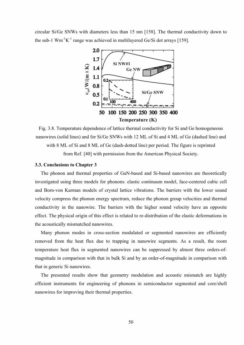
50
circular Si/Ge SNWs with diameters less than 15 nm [158]. The thermal conductivity down to
the sub-1 Wm-1K-1 range was achieved in multilayered Ge/Si dot arrays [159].
Fig. 3.8. Temperature dependence of lattice thermal conductivity for Si and Ge homogeneous
nanowires (solid lines) and for Si/Ge SNWs with 12 ML of Si and 4 ML of Ge (dashed line) and
with 8 ML of Si and 8 ML of Ge (dash-dotted line) per period. The figure is reprinted
from Ref. [40] with permission from the American Physical Society.
3.3. Conclusions to Chapter 3
The phonon and thermal properties of GaN-based and Si-based nanowires are theoretically
investigated using three models for phonons: elastic continuum model, face-centered cubic cell
and Born-von Karman models of crystal lattice vibrations. The barriers with the lower sound
velocity compress the phonon energy spectrum, reduce the phonon group velocities and thermal
conductivity in the nanowire. The barriers with the higher sound velocity have an opposite
effect. The physical origin of this effect is related to re-distribution of the elastic deformations in
the acoustically mismatched nanowires.
Many phonon modes in cross-section modulated or segmented nanowires are efficiently
removed from the heat flux due to trapping in nanowire segments. As a result, the room
temperature heat flux in segmented nanowires can be suppressed by almost three orders-of-
magnitude in comparison with that in bulk Si and by an order-of-magnitude in comparison with
that in generic Si nanowires.
The presented results show that geometry modulation and acoustic mismatch are highly
efficient instruments for engineering of phonons in semiconductor segmented and core/shell
nanowires for improving their thermal properties.

51
4. PHONON ENGINEERING IN GRAPHENE
This Chapter reviews theoretical results on phonon and thermal properties of graphene and
few-layer graphene, discusses two theoretical approaches for calculation of the phonon thermal
conductivity in graphene and describes specifics of 2D phonon transport. The Chapter is mostly
based on author’s original papers dedicated to various aspects of heat conduction in graphene
and few-layer graphene [6, 29, 49, 54, 56-58, 95, 125, 160, 161].
4.1. Phonons in graphene
The honeycomb crystal lattice of single-layer graphene (SLG) is presented in Figure 4.1(a).
The rhombic unit cell, shown as a dashed region, can be defined by two basis vectors
1 (3, 3) / 2,a a
and 2 (3, 3) / 2a a
, where a = 0.142 nm is the distance between two nearest
carbon atoms. The empty and black circles in Figure 4.1(a) denote the atoms, which belong to
the first and second Bravais lattice, respectively. The atom 01 of the first Bravais lattice is
surrounded by three atoms 0(1 , 2,3) of the second Bravais lattice. The inside dashed circle
indicate the first interaction sphere, which includes the nearest-neighbor (N) atoms of the atom
01 with the coordinates given by the radius-vectors 0 0[1 ;1 ] (1,0),R a
and
0[2(3);1 ] ( 1, 3) / 2R a
. The atoms of the second interaction sphere, shown by a dashed
circle with a larger diameter, are denoted as the far-distance-neighbors (F). They belong to the
same Bravais lattice as the central atom 01 and defined by the radius-vectors
0 0[1(4);1 )] (0, 3); [2(5);1 ]R a R
( 3, 3) / 2;a and 0[3,(6);1 ] (3, 3) / 2R a
.
The unit cell of single layer graphene consists of two atoms (see Figure 4.1 (a)), therefore 6
phonon polarization branches are in SLG. They are (i) out-of-plane acoustic (ZA) and out-of-
plane optical (ZO) phonons with the displacement vector along the Z axis; (ii) transverse
acoustic (TA) and transverse optical (TO) phonons, which corresponds to the transverse
vibrations within the graphene plane; (iii) longitudinal acoustic (LA) and longitudinal optical
(LO) phonons, which corresponds to the longitudinal vibrations within the graphene plane. For
calculation of phonon energy dispersions we applied valence force field and Born-von Karman
models of lattice dynamics. The detailed description of these models and numerical calculation
procedure is provided in author’s original works [6, 49, 58, 160, 161]. Phonon branches of SLG,
calculated using VFF model, are depicted in Figure 4.1 (b). The presented results are in a good
agreement both with phonon energies calculated using other theoretical approaches and those
obtained experimentally [4, 5, 162].

52
Fig. 4.1. (a) Graphene crystal lattice. The rombic unit cell is shown as a shaded region. (b)
Phonon dispersion in graphene calculated using the valence force field model. The figure is
adopted from Ref. [6] with permission from American Physical Society.
The unit cell of the n-layer Bernal stacking graphene contains 2n atoms, therefore 6n phonon
branches appear in n-layer graphene. Phonon dispersions in bilayer graphene, calculated using
VFF model, is shown in Figure 4.2 (a-b). Weak Van der Waals interaction between monolayers
leads to the coupling of long wavelength phonons only and quantization of the low-energy part
of the spectrum with q<0.1qmax for LA, TA, LO, TO and ZO phonons and with q<0.4qmax for ZA
phonons (see Figure 4.2 (b)). The modification of the phonon energy spectrum in n-layer
graphene as compared with that in single layer graphene results in a substantial change of the
three-phonon scattering rates and a reduction of the intrinsic thermal conductivity in n-layer
graphene [6, 29, 54, 66-67, 95].
In recent years the interest of the physics community has been shifting toward investigation of
the twisted few-layer graphene (T-FLG) systems. When two graphene layers are placed on top of
each other they can form a Moire pattern [163-165]. In this case, one layer is rotated relative to
another layer by an arbitrary angle. The samples of Moire patterns in twisted bilayer graphene
are shown in Figure 4.3. The synthesis of T-FLG was experimentally demonstrated using the
chemical vapor deposition (CVD), mechanical exfoliation or growth on the carbon terminated
SiC surface [140, 164-167]. Although twisting only weakly affects the interlayer interaction, it
breaks symmetry of the Bernal-stacking resulting in an intriguing dependence of the electronic
and phonon properties on the rotation angle (RA).
(a) (b)

53
Fig. 4.2. Phonon dispersion in bilayer graphene calculated using the VFF model. Figure is
reprinted from Ref. [54] with permission from Nature Publishing Group.
The phonon dispersions along Г-K direction in Brillouin zone in SLG, AA-stacked bilayer
graphene (AA-BLG), AB-stacked bilayer graphene (AB-BLG) and T-BLG with the rotation
angles 21.8 and 13.7 are shown in Figure 4.4. The phonon frequencies were
calculated using BvK model of lattice vibrations for each phonon wave number q from the
interval 0 to max ( )q , where max ( )q is given by:
max max( ) 2 ( 0)sin / 2 8 sin( / 2) /(3 3 )q q a . (4.1)
The directions in BZ of T-BLG depend strongly on the rotational angle and do not coincide with
the directions in BZ of SLG or BLG. Therefore, the phonon curves in Figure 4.4 are shown for
different directions in BZ of BLG. However, the Г- and K-points in BZ of T-BLG correspond to
those in BZ of BLG and the change of the phonon modes in these points is a direct effect of the
twisting.
Fig. 4.3. Moire’s patterns in twisted bilayer graphene.

54
Fig. 4.4. Phonon energy dispersions in single layer graphene (a), AA-stacked bilayer graphene
(b), and in the twisted bilayer graphene with 021.8 (c) and 013.2 (d). All dispersion
relations are shown for Г – K direction in the Brillouin zone of SLG, BLG and T-BLG,
correspondingly. Figure is reprinted from Ref. [58] with permission
from the American Physical Society.
Six pairs of phonon branches in BLG: LA1/LA2, TA1/TA2, ZA1/ZA2, LO1/LO2, TO1/TO2 and
ZO1/ZO2 can be understood as the “bilayer” analogs of LA, TA, ZA, LO, TO and ZO
polarizations of SLG. The energy difference between the phonon branches in the pairs is
small due to the weak van der Waals coupling. It attains its maximum value max at the BZ
center: -1max max(LA) (TA) 13.4 cm , -1
max (ZA) 95 cm , -1max max(LO) (TO) 0.1cm
and -1max (ZO) 1.5cm .
The in-plane interactions in BLG are much stronger than the weak van der Waals out-of-plane
interactions. For this reason, the deviation of the phonon frequencies in BLG from those in SLG
is very small (with exception of ZA2 mode). Similar results were reported for SLG and BLG
using the DFT [168], valence force field model of lattice dynamics [54, 95] and the optimized
Tersoff and Lennard-Jones (L-J) potentials [66]. It is important to note here that although various
theoretical approaches can predict different energies for LA, TA and ZA phonons at the Г – point
[6, 11, 29, 54, 85, 95, 168, 169], the descriptions of the phonon mode behavior and the
dispersion trends are consistent among the different models. The use of the L-J potential for the

55
description of the inter-layer interaction in FLG usually leads to softening of the low-frequencies
modes near the BZ center while the frequencies of all other modes are described accurately.
The twisting influences the phonon spectra of BLG owing to two reasons: (i) modification of
the weak van der Waals inter-layer interaction and (ii) alteration of a size of a BZ leading to the
phonon momentum change. Therefore, in the twisted bilayer graphene appear hybrid folded
phonon branches resulting from mixing of different directions from unrotated BLG BZ.
4.2. Lattice thermal conductivity in graphene
We now address in more detail some specifics of the acoustic phonon transport in 2D
systems. Investigation of the heat conduction in graphene [47, 48] and CNTs [170] raised the
issue of ambiguity in the definition of the intrinsic thermal conductivity for 2D and 1D crystal
lattices. It was theoretically shown that the intrinsic thermal conductivity limited by the crystal
anharmonicity has a finite value in 3D bulk crystals [171]. However, many theoretical models
predict that the intrinsic thermal conductivity reveals a logarithmic divergence in strictly 2D
systems, κ~ln(N), and the power-law divergence in 1D systems, κ~Nα, with the number of atoms
N (0<α<1) [171-173]. The logarithmic divergence can be removed by introduction of the
extrinsic scattering mechanisms such as scattering from defects or coupling to the substrate [57].
Alternatively, one can define the intrinsic thermal conductivity of a 2D crystal for a given size of
the crystal.
Graphene is not an ideal 2D crystal, considered in most of the theoretical works, since
graphene atoms vibrate in three directions. Nevertheless, the intrinsic graphene thermal
conductivity strongly depends on the graphene sheet size due to weak scattering of the low-
energy phonons by other phonons in the system. Therefore, the phonon boundary scattering is an
important mechanism for phonon relaxation in graphene. Different studies [57, 174, 175] also
suggested that an accurate accounting of the higher-order anharmonic processes, i.e. above three-
phonon Umklapp scattering, and inclusion of the normal phonon processes into consideration
allow one to limit the low-energy phonon MFP. The normal phonon processes do not contribute
directly to thermal resistance but affect the phonon mode distribution [57, 66]. However, even
these studies found that the graphene sample has to be very large (>10 µm) to obtain the size-
independent thermal conductivity.
In BTE approach within relaxation time approximation the thermal conductivity in quasi 2D
system are given by Equation (1.31). For graphene this equation can be rewritten
as follows [6, 57]:

56
max
22 2
0
( ) exp[ ( ) / ]1{[ ( ) ] ( , ) } .
4 [exp[ ( ) / ] 1]
q
s s BG s tot
sB s B
d q q k Tq s q q dq
k T h dq q k T
(4.2)
Here h = 0.335 nm is the graphene layer thickness and summation is performed over phonon
branches s.
The specific phonon transport graphene can be illustrated with a simple expression for
Umklapp – limited thermal conductivity derived in Ref. [49]. Using an expression for the three-
phonon Umklapp scattering from Refs. [90, 92] but introducing separate life-times for LA and
TA phonons, one can rewrite for the Umklapp relaxation time
2,max
, 2 2
1 ssU s
s B
M
k T
, (4.3)
where s=TA, LA, s is the average phonon velocity for a given branch, T is the absolute
temperature, kB is the Boltzmann constant, ,maxs is the maximum cut-off frequency for a given
branch and M is the mass of an unit cell. To determine γs the q-dependences of Grunaizen
parameters γ(q) calculated from the accurate phonon dispersions [5, 6] were averaged over q. To
simplify the model one can use the liner dispersion ( )s q = s q and re-write it as
2,max
,min ,max2,
( , )4
s sU s s
s TA LA s
MF
Th
, (4.4)
where
,max
,max
,min
,min
//
,min ,max /2/
( )( , ) [ { ( ) 1} ] |
[ ( ) 1] 1 ( )
s B
s B
s B
s B
k Tk T
s s k Tk T
exp x xF x dx ln exp x x
exp x exp x
. (4.5)
In the above equation, / Bx k T , and the upper cut-off frequencies ωs,max are defined from
the actual phonon dispersion. The low-bound cut-off frequencies ωs,min for each s are determined
from the condition that the phonon MFP cannot exceed the physical size L of the flake, i.e.
,max,min
ss ss
s B
M
k T L
. (4.6)
The integrand in Equation (4.5) can be further simplified near RT when ,maxs > kBT, and it
can be expressed as
,min ,min,min ,min
,min
( / )( ) {| ( / ) 1|}
( / ) 1s s B
s s BB s B
exp k TF ln exp k T
k T exp k T
(4.7)
The obtained Equations (4.4) and (4.7) constitute a simple analytical model for calculation of
the thermal conductivity of graphene layers, which retains such important features of graphene
phonon spectra as different s and γs for LA and TA branches. The model also reflects strictly 2D
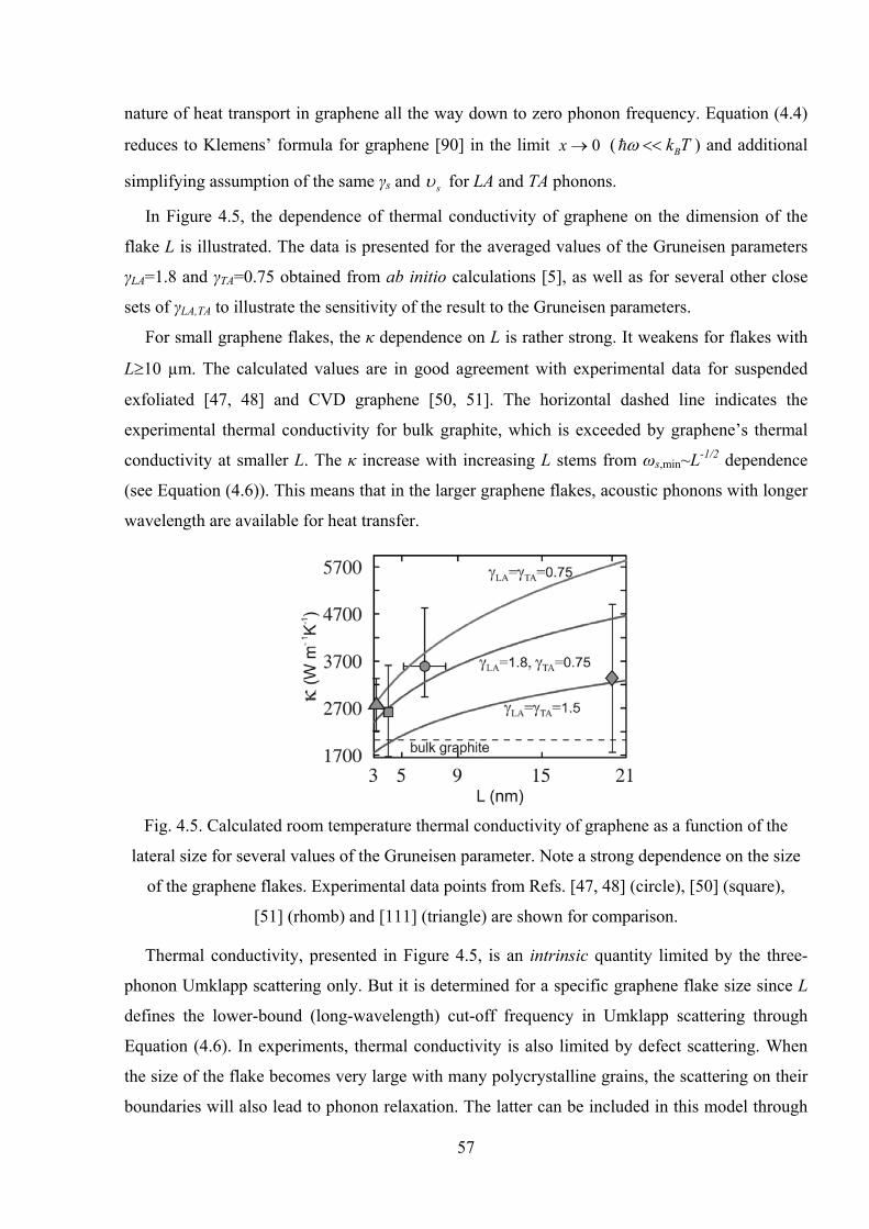
57
nature of heat transport in graphene all the way down to zero phonon frequency. Equation (4.4)
reduces to Klemens’ formula for graphene [90] in the limit 0x ( Bk T ) and additional
simplifying assumption of the same γs and s for LA and TA phonons.
In Figure 4.5, the dependence of thermal conductivity of graphene on the dimension of the
flake L is illustrated. The data is presented for the averaged values of the Gruneisen parameters
γLA=1.8 and γTA=0.75 obtained from ab initio calculations [5], as well as for several other close
sets of γLA,TA to illustrate the sensitivity of the result to the Gruneisen parameters.
For small graphene flakes, the κ dependence on L is rather strong. It weakens for flakes with
L10 µm. The calculated values are in good agreement with experimental data for suspended
exfoliated [47, 48] and CVD graphene [50, 51]. The horizontal dashed line indicates the
experimental thermal conductivity for bulk graphite, which is exceeded by graphene’s thermal
conductivity at smaller L. The κ increase with increasing L stems from ωs,min~L-1/2 dependence
(see Equation (4.6)). This means that in the larger graphene flakes, acoustic phonons with longer
wavelength are available for heat transfer.
Fig. 4.5. Calculated room temperature thermal conductivity of graphene as a function of the
lateral size for several values of the Gruneisen parameter. Note a strong dependence on the size
of the graphene flakes. Experimental data points from Refs. [47, 48] (circle), [50] (square),
[51] (rhomb) and [111] (triangle) are shown for comparison.
Thermal conductivity, presented in Figure 4.5, is an intrinsic quantity limited by the three-
phonon Umklapp scattering only. But it is determined for a specific graphene flake size since L
defines the lower-bound (long-wavelength) cut-off frequency in Umklapp scattering through
Equation (4.6). In experiments, thermal conductivity is also limited by defect scattering. When
the size of the flake becomes very large with many polycrystalline grains, the scattering on their
boundaries will also lead to phonon relaxation. The latter can be included in this model through

58
adjustment of L. The extrinsic phonon scattering mechanisms or high-order phonon-phonon
scatterings prevent indefinite growth of thermal conductivity of graphene with L [57].
The simple model described above is based on the Klemens-like expressions for the
relaxation time (see Refs. [90, 92]). Therefore it does not take into account all peculiarities of the
2D three-phonon Umklapp processes in SLG or FLG, which are important for the accurate
description of thermal transport. There are two types of the three-phonon Umklapp scattering
processes [176]. The first type is the scattering when a phonon with the wave vector ( )q
absorbs another phonon from the heat flux with the wave vector ( )q , forming the phonon with
wave vector ( )q in one of the nearest Brillouin zones. For this type of scattering processes
the momentum and energy conservation laws are written as:
( ) ( ) ( ), 1,2,3iq q b q i
. (4.8)
The processes of the second type are those when the phonons ( )q of the heat flux decay into
two phonons with the wave vectors ( )q and ( )q
, i.e. leaves the state ( )q , or,
alternatively, two phonons ( )q and ( )q
merge together forming a phonon with the wave
vector ( )q , which correspond to the phonon coming to the state ( )q . The conservation laws
for this type are given by:
( ) ( ) ( ), 1,2,3iq b q q i
. (4.9)
In Equations (4.8-4.9) , 1, 2,..., 6i ib ГГ i
is one of the vectors of the reciprocal lattice.
Calculations of the thermal conductivity in graphene taking into account all possible three-
phonon Umklapp processes allowed by the Equations (4.8-4.9) and actual phonon dispersions
were carried out in Ref. [6]. For each phonon mode ( ,q s
), were found all pairs of the phonon
modes ( ,q s ) and ( ,q s
) such that the conditions of Equations (4.8-4.9) are met. As a result, in
( q
)-space were constructed the phase diagrams for all allowed three-phonon transitions [6].
Using the long-wave approximation for a matrix element of the three-phonon interaction
[138] one can obtain for the Umklapp scattering rates [6]:
2
' 0( ),( ) 2;
0
( )1( ) ( ) ( ) { [ ( )]
( , ) 3 ( )
1 1[ ( )] } [ ( ) ( ) ( )] .
2 2
i
ss s s sI II
s s bU s
s s s s l
qq q q N q
s q q
N q q q q dq dq
(4.10)

59
In Equation (4.10) the upper signs correspond to the processes of the first type while the
lower signs correspond to those of the second type. The integrals for ,lq q are taken along and
perpendicular to the curve segments, correspondingly, where the conditions of
Equations (4.8-4.9) are met. The main mechanisms of phonon scattering in graphene are phonon-
phonon Umklapp (U) scattering, rough edge scattering (boundary (B)) and point-defect (PD)
scattering:
1/ ( , ) 1/ ( , ) 1/ ( , ) 1/ ( , ),tot U B PDs q s q s q s q (4.11)
where 1/ 1/ 1/ ,I IIU U U 1/ ( , ) ( / )((1 ) /(1 ))B ss q L p p and 2
01/ ( , ) /(4 ).PD s s ss q S q
Here /s sd dq is the phonon group velocity, p is the specularity parameter of rough edge
scattering, S is the surface per atom and is the measure of the strength of the point defect
scattering.
Fig. 4.6. Thermal conductivity of graphene over a wide temperature range calculated for the
graphene flake with the width of 5 m and mode-dependent Grunesien parameter. The results
are obtained for two values of the specularity parameter p=0.9 and point-defect scattering
strength . An experimental data point after Refs. [50, 51] is also shown for comparison. Figure
is reprinted from Ref. [6] with permission from American Physical Society.
Figure 4.6 presents the calculated thermal conductivity of graphene over a wide temperature
range with taking into account total phonon relaxation time from Equation (4.11). In the low-
temperature limit the thermal conductivity increases rapidly with increasing temperature as the
number of phonons increase. The decrease in the thermal conductivity with temperature, which
starts around 80 K is due to the growing strength of the Umklapp scattering processes. It is
interesting to note that the thermal conductivity in the low-temperature limit is proportional to
T2. Indeed, for the curve calculated with p=0.9, the ratio κ(T=80 K)/ κ(T=50 K) = 2.50, while the

60
ratio of the temperatures squared is (80/50)2=2.56. This is a manifestation of the 2D nature of
graphene. In bulk the low-temperature thermal conductivity is proportional to ~T3. The
difference in the temperature dependence between the 2D graphene and bulk materials is related
to the different phonon density of states. Small deviation from T2 dependence in our case is
explained by the fact that the considered temperature is not low enough (~50-80 K) and by the
presence of other scattering mechanisms, e.g. phonon – boundary scattering. The latter is
confirmed by the growing deviation as p decreases farther down from unity.
Fig. 4.7. (a) Thermal conductivity as a function of the number of atomic planes in few-layer
graphene. The dashed straight lines indicate the range of bulk graphite thermal conductivities.
The circles correspond to the experimental data, while diamonds shows the theoretical values,
calculated from the accurate theory of thermal conduction in few-layer graphene based on the
actual phonon dispersion and accounting for all allowed three-phonon Umklapp scattering
channels (see Equation (4.9-4.11)). The green triangles are Callaway–Klemens model
calculations, which include extrinsic effects characteristic for thicker films. (b) Diagram of three-
phonon Umklapp scattering in graphene and bi-layer graphene (BLG), which shows that in BLG
there are more states available for scattering owing to the increased number of phonon branches.
Figure is adopted from Ref. [54] with permission from the Nature Publishing Group.
In conventional semiconductor thin films the in-plane thermal conductivity decreases with
decreasing thickness because the thermal transport in such structures is mostly limited by the
phonon scattering from the film boundaries [8, 123, 124, 129]. An opposite dependence can be
observed in suspended few-layer graphene (FLG) where the transport is limited mostly by the
lattice anharmonicity [54]. Figure 4.7 shows that the thermal conductivity of the suspended
uncapped FLG decreases with increasing number of the atomic layers n and approaches the bulk

61
graphite limit. The experimentally observed evolution of the thermal conductivity in FLG
(indicated by circles in the graph) is explained theoretically by considering the intrinsic quasi 2D
crystal properties described by the phonon Umklapp scattering. As n in FLG increases – the
additional phonon branches for the heat transfer appear (see Figure 4.2.), while, at the same time,
more phase-space states become available for the phonon scattering (see Figure 4.7 (b)). As a
result the thermal conductivity decreases. The thermal conductivity dependence on the FLG
thickness can be entirely different for encased FLG, where thermal transport is limited by the
acoustic phonon scattering from the top and bottom boundaries and disorder. An experimental
study [120] found K≈160 Wm-1K-1 for encased graphene at T=310 K. It increases
to ~1000 Wm-1K-1 for graphite films with the thickness of 8 nm.
4.3. Lattice thermal conductivity in graphene ribbons
The schematic view of a suspended graphene ribbon is shown in Figure 4.8. In order to study
the thermal conductivity dependence on the lateral size of the graphene ribbon we consider the
phonon anharmonic interactions to the second order and the angle dependence of the phonon
scattering from the ribbon edges. We specifically focus on ribbons with the micrometer width d
and length L in order to deal with the actual phonon dispersion in graphene and to ensure the
diffusive transport regime. In the nanometer-thick graphene ribbons the phonon dispersion is
different owing to the phonon mode quantization and the lateral size dependence is dictated by
the ballistic conduction [115]. The total phonon scattering rate for the phonon mode (s, q) is
given as [57]:
21/ ( , ) 1/ ( , ) 1/ ( , ) 1/ ( , ),tot U Bs q s q s q s q
(4.12)
where 2,s is the mode-dependent three-phonon Umklapp scattering rate calculated to the second
order [57, 174] and ||( , , ) / ( )B b ss q p q
is the phonon mode-dependent boundary scattering
rate. The calculation of ,U s is performed using Equation (4.10). The phonon mode-dependent
MFP ( , , )b s q p
limited by the boundary scattering is calculated as a function of the angle
between q
and the thermal gradient for each phonon mode. Therefore in the case of rectangular
ribbon B depends both on L and d (see Figure 4.8 (b)).
In order to evaluate 2 ( , )s q we include the following processes: the long-wavelength phonon
q
interacts with the short-wavelength phonon 'q
in the normal process forming a phonon iq
.
The phonon iq
then interacts with the phonon ''q
in the Umklapp process forming a phonon
'''.q
The scattering rate of such processes in graphene takes the form

62
2
4 4 2|| 2
2,
1 32( ) ( ') ( ) ' ''
9 ( ) 2B
ss s
k T adq dq
M
(4.13)
Fig. 4.8. (a) Schematics of a typical suspended graphene ribbon used for experimental studies of
thermal transport in suspended graphene ribbons. (b) Graphene ribbon and notations used in the
present model for accounting the angle-dependent phonon scattering from the ribbon edges. The
figure is reprinted from Ref. [57] with permission from American Chemical Society.
Equation (4.13) was derived following the approach described in Ref. [174] and taking into
account 2D phonon density of states in graphene [57]. Considering all possible three-phonon
processes in graphene, it was found that in the normal processes with the long-wavelength
phonons max| | 0.05q q , intensively participate phonons with | ' |q
~(0.6-0.7)qmax, forming the
phonons | |iq ~(0.55-0.75)qmax, while in the Umklapp processes, the phonons | |iq intensively
interact with the phonons | ''q
|~(0.5-0.7)qmax. Therefore, one can assume that for the most
intensive second-order processes | ' |q
is close to (0.6-0.7)qmax, | ''q
| is close to (0.5-0.7)qmax , and
can rewrite Equation (4.13) as follows
2
4max,|| 2
2,
1 2.
9 ( )B
s ss s
k T
M
(4.14)
Figure 4.9 shows the dependence of the RT phonon thermal conductivity of the rectangular
graphene ribbon on the ribbon length L for different specular parameters p and the ribbon width
d. The long-wavelength phonons weakly participate in three-phonon Umklapp processes.
Therefore, their contribution to the thermal conductivity is mostly limited by the boundary
scattering up to the length scale L ~ 100 μm. For L>100 μm the second order anharmonic
processes become the main scattering mechanism for the long wavelength phonons. The most
striking feature in Figure 4.9 is a non-monotonic dependence of the thermal conductivity on the
ribbon length L. Such an unusual κ(L) characteristic suggests that the measured thermal

63
conductivity of graphene ribbons of certain length, i.e. L/d ratios, will be higher than that of
graphene samples of other sizes and geometries.
The possibility of the non-monotonic dependence can be explained via the following
considerations. A portion of the acoustic phonons in the rectangular ribbon with the angle
2 2arcsin( / )d d L does not scatter from the ribbon edges. MFP of these phonons
/ cos( )b L is determined only by the ribbon length L (at fixed d) and schematically shown
in Figure 4.8 (b) by the dashed arrows. The rest of the phonons participate in the edge scattering
and their b depends on both L and d (schematically shown in Figure 4.8 (b) by the solid
arrows): 2 2( )b d n L if n (1+p)/(1-p) and (1 ) /(1 )b d p p otherwise, where n
shows a number of reflections from the ribbon boundary.
Fig. 4.9. (a) Dependence of the thermal conductivity of the rectangular graphene ribbon on the
ribbon length L shown for different specular parameters p. The width is fixed at d=5 µm. (b)
Dependence of the thermal conductivity of the rectangular graphene ribbon on the ribbon length
L shown for different ribbon width d. The specular parameter is fixed at p=0.9. The figure is
reprinted from Ref. [57] with permission from American Chemical Society.
The number of reflections n was calculated numerically (at fixed L, d, ) from the condition
cos( ) .b L The interplay between contributions of the above-mentioned two groups of
phonons as well as the anisotropic anharmonic scattering mechanisms leads to the predicted non-
monotonic behavior of the thermal conductivity κ(L).
At small L the phonons with the MFP limited by the length only – b (L) – are the main heat
carriers and thermal conductivity rapidly increases with L. The contribution of these type of
phonons to the thermal conductivity in graphene ribbon with d = 1 μm is shown in Figure 4.9 (b)
with the dashed line. Further increase of L decreases with the corresponding reduction of the
number of phonons with b (L) and increase of the number of phonons that have MFP dependent

64
on both L, d and p – b (L,d,p). Therefore, the contribution of the phonons with b (L,d,p)
increases (as shown in Figure 4.9 (b) with dotted line) leading to a maximum in the thermal
conductivity curve. For L>~100 μm b is mainly determined by d and the thermal conductivity
saturates to its finite value. The finite value in Figure 4.9 (b) for d=5 µm is in agreement with the
experimental data [47, 48]. The values for ribbons with large d and p1 are larger than what
was reported experimentally because the model intentionally does not include non-idealities such
as defects or grain boundaries.
Another important observation from Figure 4.9 (a) is that the abnormal non-monotonic κ(L)
dependence can only be observed in graphene ribbons with the relatively smooth edges
characterized by the specularity parameter p>0.5. The specularity parameter p=1 means that all
phonons scatter from the edges elastically preserving their momentum along the ribbon length.
The κ(L) non-monotonic dependence is also a function of the specific geometry of the ribbon via
the angle dependence on L and d. The non-monotonic character disappears in circular
geometry such as in membranes used in some of the graphene thermal experiments [50, 52].
The results obtained for the infinitely-wide ribbons ( d ) also show the monotonic
increase of κ with the saturated value for L>100 μm. This finding is in line with the predictions
made for the CNTs [175]. As in the case for CNTs, the thermal conductivity of graphene ribbons
limited only by three-phonon Umklapp scattering increases monotonically with L (see dashed-
dotted curve in Figure 4.9 (b)) without saturation to the constant value. The finite value results
from inclusion of the anharmonic three-phonon processes of the second-order.
4.4. Conclusions to Chapter 4
In this chapter the theoretical results pertinent to two-dimensional phonon transport in
graphene were reviewed. Phonons are the dominant heat carriers in the single-layer and few-
layer graphene near room temperature. The unique nature of 2D phonons translates to unusual
heat conduction in single layer and few-layer graphene. The thermal conductivity of graphene
depends strongly on extrinsic parameters: flake size and shape, quality of flake edges and defects
of crystal lattices. The presented results are important for the proposed practical applications of
graphene in heat removal and thermal management of advanced electronics and optoelectronics.

65
GENERAL CONCLUSIONS AND RECOMMENDATIONS
The summary of the results presented in the Scientific Review is given below:
1. It was theoretically shown that quasi two-dimensional and one-dimensional multilayered
semiconductor nanostructures and graphene possess many degrees of freedom for phonon
engineering: a proper tuning the phonon properties in such nanostructures leads to the
improvement of their thermal properties and enhancement of electron mobility. Thus, a
fundamentally new approach for phonon-engineered improvement of thermal and
electrical properties of semiconductor nanostructures and graphene was theoretically
developed.
2. In the framework of continuum approach and two dynamic models of lattice vibrations
(face-centered cubic cell and Born-von Karman models) it was demonstrated that
cladding layers strongly influence both phonon energy spectra and thermal conductivity
of nanofilms and nanowires. The claddings with high (low) sound velocities increase
(decrease) the average phonon group velocity and thermal flux in film/wire with
claddings in comparison with generic film/wire without claddings.
3. It was theoretically revealed that electron mobility of silicon nanolayers can be increased
by covering them with cladding layers possessing higher sound velocity than that in
silicon. The electron mobility in Diamond/Si/Diamond heterostructure with dimensions
10 nm/ 2 nm/ 10 nm is by a factor of 2 – 10 higher than that in Si nanolayer without
claddings. The increase results from phonon spectrum modification and suppression of
the deformation-potential electron-phonon scattering.
4. It was shown that two- up to fivefold enhancement of electron mobility in wurtzite
AlN/GaN/AlN planar heterostructures can be achieved by a compensation of built-in
electric field by an external electric field or by a creation of ultra-narrow InxGa1-xN
nanogroove in the middle of GaN well with small In content x ~ 0.05. The enhancement
results from change of the position of electron wave functions maximum and suppression
of electron-polar optical phonon scattering.
5. It was theoretically demonstrated that in-plane lattice thermal conductivity of single layer
graphene and few-layer graphene strongly depends on the extrinsic parameters: flake size
and shape, quality of flake edges and defects of crystal lattices. The room-temperature in-
plane lattice thermal conductivity of 5 µm – thick graphene flake with perfect edges is in
a range 3500 – 5000 Wm-1K-1. The thermal conductivity decreases rapidly with
increasing number of graphene monolayers n and approaches the highly-oriented

66
pyrolitic graphite limit for n=4. The in-plane thermal conductivity of micrometer size
rectangular graphene ribbons demonstrates non-monotonic dependence on flake size due
to the long mean-free path of long-wavelength acoustic phonons.
6. It was theoretically established that twisting bilayer graphene leads to the emergence of
hybrid folded phonons, which depend on the twisting angle and originate from the
mixing of phonon modes from different high-symmetry directions in the Brillouin zone.
Based on the presented results, the following recommendation can be formulated:
Practical implementation of nanoscale phonon engineering concept may improve both
operational parameters of modern nanostructure-based devices and thermal management
in modern electronic circuits;
The novel phonon-optimized nanostructures like as segmented or cross-section-
modulated nanowires are promising candidates for thermoelectric and thermo insulating
applications;
Graphene and graphene –based materials are good candidates for optimized heat removal
and efficient thermal management in modern electronic devices and circuits.
The obtained theoretical results shed light on the peculiarities of phonon heat conduction at
nanoscale and contribute to deeper understanding of phonon transport and phonon-assisted
processes in quasi one- and two-dimensional semiconductor nanostructures and graphene.

67
REFERENCES
1. Ziman J. Electrons and Phonons: The Theory of Transport Phenomena in Solids. New
York: Oxford University Press, 1960. 554 p.
2. Anselm A. Introduction to semiconductor theory. Moscow: Mir Publishers, 1981. 490 p.
3. Stroscio M., Dutta M. Phonons in Nanostructures. Cambridge: Cambridge University
Press, 2001. 282 p.
4. Wirtz L. and Rubio A. The phonon dispersion of graphite revisited. In: Solid State
Communications, 2004, vol. 131, p. 141-152.
5. Mounet N. and Marzari N. First-principles determination of the structural, vibrational and
thermodynamic properties of diamond, graphite, and derivatives. In: Physical Review B,
2005, vol. 71, p. 205214.
6. Nika D. et al. Phonon thermal conduction in graphene: role of Umklapp and edge
roughness scattering. In: Physical Review B, 2009, vol. 79, p. 155413.
7. Balandin A., and Wang K. Effect of phonon confinement on the thermoelectric figure of
merit of quantum wells. In: Journal of Applied Physics, 1998, vol. 84, p. 6149-6153.
8. Balandin A., and Wang K. Significant decrease of the lattice thermal conductivity due to
phonon confinement in a free-standing semiconductor quantum well. In: Physical Review
B, 1998, vol. 58, 3, p. 1544.
9. Balandin A., Pokatilov E., Nika D. Phonon Engineering in Hetero- and Nanostructures.
In: Journal of Nanoelectronics and Optoelectronics, 2007, vol. 2, p. 140-170.
10. Klitsner T. and Pohl R. Phonon scattering at silicon crystal surfaces. In: Physical Review
B, 1987, vol. 36, p. 6551-6565.
11. Pokatilov E., Nika D., Balandin A. A phonon depletion effect in ultrathin heterostructures
with acoustically mismatched layers In: Applied Physics Letters, 2004, vol. 85, p. 825-
827.
12. Pokatilov E., Nika D., Balandin A. Acoustic-phonon propagation in rectangular
semiconductor nanowires with elastically dissimilar barriers. In: Physical Review B,
2005, 72, p. 113311.
13. Pokatilov E., Nika D., Balandin A. Acoustic phonon engineering in coated cylindrical
nanowires. In: Superlattices and Microstructures, 2005, vol. 38, p. 168-183.
14. Pokatilov E., Nika D., and Balandin A. Confined electron-confined phonon scattering
rates in wurtzite AlN/GaN/AlN heterostructures. In: Journal of Applied Physics, 2004,
vol. 95, p. 5626-5632.

68
15. Pokatilov E., Nika D., Balandin A. et al. Phonon spectrum and group velocities in
AlN/GaN/AlN and related heterostructures. In: Superlattices and Microstructures, 2003,
vol. 33, 155-171.
16. Benisty H., Sotomayor-Torres C., Weisbuch C. Intrinsic mechanism for the poor
luminescence properties of quantum-box systems In: Physical Review B, 1991, vol. 44, p.
10945.
17. Klimin S., Pokatilov E., Fomin V. Polaronic hamiltonian and polar optical vibrations in
multilayer structures. Physica Status Solidi (b), 1995, 190, 441-453.
18. Pokatilov E. et al. Excitons in wurtzite AlGaN⁄GaN quantum-well heterostructures. In:
Physical Review B, 2008, vol. 77, 125328
19. Rytov S. Acoustical properties of a thinly laminated medium. In: Soviet Physics –
Acoustics, 1956, vol. 2, p. 67-80.
20. Colvard C. et al. Folded acoustic and quantized optic phonons in (GaAl)As superlattices.
In: Physical Review B, 1985, vol. 31, p. 2080.
21. Bannov N., Mitin V., Stroscio M. Confined acoustic phonons in a free-standing quantum
well and their interaction with electrons. In: Physica Status Solidi (b), 1994, vol. 183, p.
131-142.
22. Nishiguchi N., Ando Y., Wybourne M. Acoustic phonon modes of rectangular quantum
wires. In: Journal of Physics: Condensed Matter, 1997, vol. 9, p. 5751.
23. Svizhenko A. et al. Electron interaction with confined acoustic phonons in quantum wires
subjected to a magnetic field. In: Physical Review B, 1998, vol. 57, p. 4687.
24. Veliadis J. et al. Engineering of the nonradiative transition rates in modulation-doped
multiple-quantum wells. In: IEEE Journal of Quantum Electronics, 1996, vol. 32, p.
1155-1160.
25. Zou J., Balandin A. Phonon heat conduction in a semiconductor nanowire. In: Journal of
Applied Physics, 2001, vol. 89, p. 2932.
26. Khitun A., Balandin A., Wang K. Modification of the thermal conductivity in silicon
quantum wires due to spatial confinement of acoustic phonons. In: Superlattices and
Microstructures, 1999, vol. 26, p. 181-193.
27. Khitun A. et al. Enhancement of the thermoelectric figure of merit of Si1-xGex quantum
wires due to spatial confinement of acoustic phonons. In: Physica E, 2000, vol. 8, p. 13-
18.
28. Khitun A. et al. In-plane lattice thermal conductivity of a quantum-dot superlattice. In:
Journal of Applied Physics, 2000, vol. 88, p. 696-699.

69
29. Balandin A., Nika D. Phononics in low-dimensional materials. In: Materials Today, 2012,
vol. 15, p. 266-275.
30. Balandin A. Thermoelectric applications of low-dimensional structures with acoustically
mismatched boundaries. In: Physics of Low-Dimensional Structures, 2000, vol. 5/6, p.
73-91.
31. Casian A. et al. Thermoelectric properties of n-type PbTe/Pb1-xEuxTe quantum wells. In:
Physical Review B, 2000, vol. 61, p. 15965 – 15974.
32. Casian A., Sanduleac I. Thermoelectric Properties of Tetrathiotetracene Iodide Crystals:
Modeling and Experiment. In: Journal of Electronic Materials, 2014, vol. 43, p. 3740 –
3745.
33. Sakaki, H. Scattering suppression and high-mobility effect of size-quantized electrons in
ultrafine semiconductor wire structures. In: Japanese Journal of Applied Physics, 1980,
vol. 19, p. L735-L738.
34. Fonoberov V., Balandin A. Giant enhancement of the carrier mobility in silicon
nanowires with diamond coating. In: Nano Letters, 2006, vol. 6, p. 2442-2446.
35. Nika D., Pokatilov E., Balandin A. Phonon-engineered mobility enhancement in the
acoustically mismatched silicon/diamond transistor channels. In: Applied Physics Letters,
2008, vol. 93, p. 173111.
36. Zincenco N. et al. Acoustic phonon engineering of thermal properties of silicon-based
nanostructures. In: Journal of Physics: Conference Series. 2007, vol. 92, p. 012086.
37. Nika D., Zincenco N., Pokatilov E. Engineering of thermal fluxes in phonon mismatched
heterostructures. In: Journal of Nanoelectronics and Optoelectronics, 2009, vol. 4, p. 180-
185.
38. Lazarenkova O., Balandin A. Electron and phonon energy spectra in a three-dimensional
regimented quantum dot superlattice. In: Physical Review B, 2002, vol. 66, p. 245319.
39. Balandin A. and Lazarenkova O. Mechanism for thermoelectric figure-of-merit
enhancement in regimented quantum dot superlattices. In: Applied Physics Letters, 2003,
vol. 82, p. 415-417.
40. Nika D. et al. Reduction of lattice thermal conductivity in one-dimensional quantum-dot
superlattices due to phonon filtering. In: Physical Review B, 2011, vol. 84, p. 165415.
41. Pokatilov E., Nika D., Balandin A. Biuld-in filed effect on the electron mobility in
AlN/GaN/AlN quantum wells. In: Applied Physics Letters, 2006, vol. 89, p. 113508.

70
42. Pokatilov E., Nika D., Balandin A. Electron mobility enhancement in AlN/GaN/AlN
heterostructures with InGaN nanogrooves. In: Applied Physics Letters, 2006, vol. 89, p.
112110.
43. Pokatilov E. et al. Size-quantized oscillations of the electron mobility limited by the
optical and confined acoustic phonons in the nanoscale heterostructures. In:Journal of
Applied Physics, 2007, vol. 102, p. 054304.
44. Hu M. et al. Significant reduction of thermal conductivity in si/ge core−shell nanowires.
In: Nano Letters, 2011, vol. 11, p. 618-623.
45. Wingert M. et al. Thermal conductivity of Ge and Ge–Si core–shell nanowires in the
phonon confinement regime. In: Nano Letters, 2011, vol. 11, p. 5507-5513.
46. Balandin A. Themal properties of graphene and nanostructured carbon materials. In:
Nature Materials, 2011, vol. 10, p. 569-581.
47. Balandin A. et al. Superior thermal conductivity of single-layer graphene. In: Nano
Letters, 2008, vol. 8, p. 902-907.
48. Ghosh S. et al. Extremely high thermal conductivity in graphene: Prospects for thermal
management application in nanoelectronic circuits. In: Applied Physics Letters, 2008,
vol. 92, p. 151911.
49. Nika D. et al. Lattice thermal conductivity of graphene flakes: comparison with bulk
graphite. In: Applied Physics Letters, 2009, vol. 94, p. 203103.
50. Cai W. et al. Thermal transport in suspended and supported monolayer graphene grown
by chemical vapor deposition. In: Nano Letters, 2010, vol. 10, p. 1645-1651.
51. Jauregui L. et al. Thermal transport in graphene nanostructures: experiments and
simulations. In: ECS Transactions, 2010, vol. 28, p. 73-83.
52. Faugeras C. et al. Thermal conductivity of graphene in Corbino membrane geometry. In:
ACS Nano, 2010, vol. 4, p. 1889-1892.
53. Seol J. et al. Two-dimensional phonon transport in supported graphene. In: Science,
2010, vol. 328, p. 213-216.
54. Ghosh S. et al. Dimensional crossover of thermal transport in few-layer graphene. In:
Nature Materials, 2010, vol. 9, p. 555-558.
55. Maultzsch J. et al. Phonon dispersion in graphite. In: Physical Review Letters, 2004, vol.
92, p. 075501-1-4.
56. Nika D., Pokatilov E., Balandin A. Theoretical description of thermal transport in
graphene: The issue of phonon cut-off frequencies and polarization branches. In: Physica
Status Solidi B, 2011, vol. 248, p. 2609-2614.

71
57. Nika D., Askerov A., Balandin A. Anomalous size dependence of the thermal
conductivity graphene ribbons. In: Nano Letters, 2012, vol. 12, p. 3238-3244.
58. Cocemasov A., Nika D., Balandin A. Phonons in twisted bilayer graphene. In: Physical
Review B, 2013, vol. 88, p. 035428-1-12.
59. Falkovsky L.A. Symmetry constraints on phonon dispersion in graphene. In: Physics
Letters A, 2008, vol. 372, p. 5189-5192.
60. Perebeinos V., Tersoff J. Valence force model for phonons in graphene and carbon
nanotubes. In: Physical Review B, 2009, vol. 79, p. 241409(R).
61. Alofi A., Srivastava G. Phonon conductivity in graphene. In: Journal of Applied Physics,
2012, vol. 112, p. 013517.
62. Droth M., Burkard G. Acoustic phonon and spin relaxation in graphene nanoribbons. In:
Physical Review B, 2011, vol. 84, p. 155404.
63. Qian J., et al. Quantized long-wavelength optical phonon modes in graphene nanoribbon
in the elastic continuum model. In: Superlattices and Microstructures, 2009, vol. 46, p.
881-888.
64. Yan J-A., Ruan W.Y., Chou M.Y. Phonon dispersions and vibrational properties of
monolayer, bilayer, and trilayer graphene: density-functional perturbation theory. In:
Physical Review B, 2008, vol. 77, p. 125401.
65. Wang H. et al. Vibrational properties of graphene and graphene layers. In: Journal of
Raman Spectroscopy, 2009, vol. 40, p. 1791-1796.
66. Lindsay L., Broido D., Mingo N. Flexural phonons and thermal transport in multilayer
graphene and graphite. In: Physical Review B, 2011, vol. 83, p. 235428.
67. Singh D., Murthy J., Fisher T. Mechanism of thermal conductivity reduction in few-layer
graphene. In: Journal of Applied Physics, 2011, vol. 110, p. 044317.
68. Lindsay L., Broido D. Optimized Tersoff and Brenner empirical potential parameters for
lattice dynamics and phonon thermal transport in carbon nanotubes and graphene. In:
Physical Review B, 2010, vol. 81, p. 205441.
69. Evans W., Hu L., Keblinsky P. Thermal conductivity of graphene ribbons from
equilibrium molecular dynamics: effect of ribbon width, edge roughness, and hydrogen
termination. In: Applied Physics Letters, 2010, vol. 96, p. 203112.
70. Zhong W. et al. Chirality and thickness-dependent thermal conductivity of few-layer
graphene: a molecular dynamics study. In: Applied Physics Letters, 2011, vol. 98, p.
113107.

72
71. Zhang H., Lee G., Cho K. Thermal transport in graphene and effects of vacancies. In:
Physical Review B, 2011, vol. 84, p. 115460.
72. Wei Z. et al. In-plane lattice thermal conductivities of multilayer graphene films. In:
Carbon, 2011, vol. 49, p. 2653-2658.
73. Ong Z.-Y., Pop E. Effect of substrate modes on thermal transport in supported graphene.
In: Physical Review B, 2011, vol. 84, p. 075471.
74. Wei N. et al. Strain engineering of thermal conductivity in graphene sheets and
nanoribbons: a demonstration of magic flexibility. In: Nanotechnology, 2011, vol. 22, p.
105705.
75. Hao F., Fang D., Xu Z. Mechanical and thermal transport properties of graphene with
defects. In: Applied Physics Letters, 2011, vol. 99, p. 041901.
76. Mortazavi B., Ahzi S. Thermal conductivity and tensile response of defective graphene:
A molecular dynamics study. In: Carbon, 2013, vol. 63, p. 460-470.
77. Ng T., Yeo J., Liu Z. A molecular dynamics study of the thermal conductivity of
graphene nanoribbons containing dispersed Stone-Thrower-Wales defects. In: Carbon,
2012, vol. 50, p. 4887-4893.
78. Jang Y. et al. Thermal conductivity of defected graphene. In: Physics Letters A, 2012,
vol. 376, p. 3668.
79. Yeo J., Liu Z., Ng T. Comparing the effects of dispersed Stone–Thrower–Wales defects
and double vacancies on the thermal conductivity of graphene nanoribbons. In:
Nanotechnology, 2012, vol. 23, p. 385702.
80. Yang D. et al. Influence of typical defects on thermal conductivity of graphene
nanoribbons: An equilibrium molecular dynamics simulation. In: Applied Surface
Science, 2012, vol. 258, p. 9926-9931.
81. Park M., Lee S., Kim Y. Length-dependent thermal conductivity of graphene and its
macroscopic limit. Journal of Applied Physics, 2013, vol. 114, p. 053506.
82. Yu C., Zhang G. Impacts of length and geometry deformation on thermal conductivity of
graphene nanoribbons. In: Journal of Applied Physics, 2013, vol. 113, p. 044306.
83. Cao A. Molecular dynamics simulation study on heat transport in monolayer graphene
sheet with various geometries. In: Journal of Applied Physics, 2012, vol. 111, p. 083528.
84. Cao H.-Y. et al. Layer and size dependence of thermal conductivity in multilayer
graphene. In: Physics Letters A, 2012, vol. 376, p. 525-528.
85. Cheng L., Kumar S. Thermal transport in graphene supported on copper. In: Journal of
Applied Physics, 2012, vol. 112, p. 043502.

73
86. Yeo P., Loh K., Gan C. Strain dependence of the heat transport properties of graphene
nanoribbons. In: Nanotechnology, 2012, vol. 23, p. 495702.
87. Ma F. et al. Strain effect on lattice vibration, heat capacity, and thermal conductivity of
graphene. In: Applied Physics Letters, 2012, vol. 101, p. 111904.
88. Huang Z., Fisher T., Murthy J. Simulation of phonon transmission through graphene and
graphene nanoribbons with a Green’s function method. In: Journal of Applied Physics,
2010, vol. 108, p. 094319.
89. Zhai X., Jin G. Stretching-enhanced ballistic thermal conductance in graphene
nanoribbons. In: EPL, 2011, vol. 96, p. 16002.
90. Klemens P. Theory of the a-plane thermal conductivity of graphite. In: Journal of Wide
Bandgap Materials, 2000, vol. 7, p. 332-339.
91. Aksamija Z., Knezevic I. Lattice thermal conductivity of graphene nanoribbons:
anisotropy and edge roughness scattering. In: Applied Physics Letters, 2011, vol. 98, p.
141919.
92. Klemens P., Pedraza D. Thermal conductivity of graphite in basal plane. In: Carbon,
1994, vol. 32, p. 735-741.
93. Adamyan V., Zavalniuk V. Lattice thermal conductivity of graphene with conventionally
isotopic defects. In: Journal of Physics: Condensed Matter, 2012, vol. 24, p. 415406.
94. Aksamija Z., Knezevic I. Thermal transport in graphene nanoribbons supported on SiO2.
In: Physical Review B, 2012, vol. 86, 165426.
95. Nika D., Balandin A. Two-dimensional phonon transport in graphene. In: Journal of
Physics: Condensed Matter, 2012, vol. 24, 233203-1-18.
96. Savin A., Kivshar Y., Hu B. Suppression of thermal conductivity in graphene
nanoribbons with rough edges. In: Physical Review B, 2010, vol. 82, p. 195422.
97. Hu J., Ruan X., Chen Y. Thermal conductivity and thermal rectification in graphene
nanoribbons: a molecular dynamic study. In: Nano Letters, 2009, vol. 9, p. 2730-2735.
98. Guo Z., Zhang D., Gong X.-G. Thermal conductivity of graphene nanoribbons. In:
Applied Physics Letters, 2009, vol. 95, p. 163103.
99. Ouyang T. et al. Thermal transport of isotopic-superlattice graphene nanoribbons with
zigzag edge. In: Europhysics Letters, 2009, vol. 88, p. 28002.
100. Chen S. et al. Thermal conductivity of isotopically modified graphene. In: Nature
Materials, 2012, vol. 11, p. 203-207.
101. Jiang J. et al. Isotopic effects on the thermal conductivity of graphene nanoribbons:
localization mechanism. In: Journal of Applied Physics, 2010, vol. 107, p. 054314.

74
102. Zhang H. et al. Isotope effect on the thermal conductivity of graphene. In: Journal of
Nanomaterials, 2010, vol. 53, p. 7657
103. Hu J. et al. Tuning the thermal conductivity of graphene nanoribbons by edge passivation
and isotope engineering: a molecular dynamics study. In: Applied Physics Letters, 2010,
vol. 97, p. 133107.
104. Jinag J.-W., Wang B.-S., Wang J.-S. First principle study of the thermal conductance in
graphene nanoribbon with vacancy and substitutional silicon defects. In: Applied Physics
Letters, 2011, vol. 98, p. 113114.
105. Hu J. et al. Nonlinear thermal transport and negative differential thermal conductance in
graphene nanoribbons. In: Applied. Physics Letters, 2011, vol. 99, p. 113101.
106. Xie Z.-X., Chen K.-Q., Duan W. Thermal transport by phonons in zigzag graphene
nanoribbons with structural defects. In: Journal of Physics: Condensed Matter, 2011, vol.
23, p. 315302.
107. Murali R. et al. Breakdown current density of graphene nanoribbons. In: Applied Physics
Letters, 2009, vol. 94, p. 243114.
108. Liao A. et al. Thermally limited current carrying ability of graphene nanoribbons. In:
Physical Review Letters, 2011, vol. 106, p. 256801.
109. Wemhoff A. A review of theoretical techniques for graphene and graphene nanoribbon
thermal conductivity prediction. In: International Journal of Transport Phenomena, 2012,
vol. 13, p. 121-141.
110. Dorgan V. et al. High-filed electric and thermal transport in suspended graphene. In:
Nano Letters, 2013, vol. 13, p. 4581-4586.
111. Li H. et al. Thermal conductivity of twisted bilayer graphene. In: Nanoscale, 2014, vol. 6,
p. 13402-13408.
112. Fu X. et al. Length-dependent thermal conductivity in suspended single-layer graphene.
In: Nature Communications, 2015, vol. 5, p. 3689.
113. Lindsay L., Broido D., Mingo N. Diameter dependence of carbon nanotube thermal
conductivity and extension to the graphene limit. In: Physical Review B, 2010, vol. 82, p.
161402.
114. Alofi A., Srivastava G. Thermal conductivity of graphene and graphite. In: Physical
Review B, 2013, vol. 87, p. 115421.
115. Munoz E., Lu J., Yakobson B. Ballistic thermal conductance of graphene ribbons. In:
Nano Letters, 2010, vol. 10, p. 1652-1656.

75
116. Jiang J-W., Wang J-S., Li B. Thermal conductance of graphite and dimerite. In: Physical
Review B, 2009, vol. 79, p. 205418.
117. Lindsay L. et al. Phonon thermal transport in strained and unstrained graphene from first
principles. In: Physical Review B, 2015, vol. 89, p. 155426.
118. Barbarino G., Melis C., Colombo L. Intrinsic thermal conductivity in monolayer
graphene is ultimately upper limit: A direct estimation by atomistic simulations. In:
Physical Review B, 2015, vol. 91, p. 035416.
119. Pettes M. et al. Influence of polymeric residue on the thermal conductivity of suspended
bilayer graphene. In: Nano Letters, 2011, vol. 11, p. 1195-1200.
120. Jang W. et al. Thickness-dependent thermal conductivity of encased graphene and
ultrathin graphite. In: Nano Letters, 2010, vol. 10, p. 3909-3913.
121. Wang Z. et al. Thermal transport in suspended and supported few-layer graphene. In:
Nano Letters, 2011, vol. 11, p. 113-118.
122. Jang W. et al. Thermal conductivity of suspended few-layer graphene by a modified T-
bridge method. In: Applied Physics Letters, 2013, vol. 103, p. 133102.
123. Cocemasov A., Nika D. Phonons and phonon thermal conductivity in silicon nanolayers.
In: Journal of Nanoelectronics and Optoelectronics, 2012, vol. 7, p. 370-375.
124. Nika D., Zincenco N., Pokatilov E. Lattice thermal conductivity of ultra-thin freestanding
layers: face-centered cubic cell model versus continuum approach. In: Journal of
Nanoelectronics and Optoelectronics, 2009, vol. 4, p. 170-173.
125. Nika D. Phonon engineering in graphene and semiconductor nanostructures. Chișinau:
CEP USM, 2015. 185 p.
126. Landau L., Lifshits E. M. Theory of Elasticity. Moscow: Fizmatlit, 2001.
127. Fedorov F.I. Theory of elastic waves in crystals. New York: Springer Science + Business
Media, 1968.
128. Li D. et al. Thermal conductivity of individual silicon nanowires. In: Applied Physics
Letters, 2003, vol. 83, p. 2934-2936.
129. Liu W., Ashegi M. Thermal conductivity measurement of ultra-thin single crystal silicon
layers. In: Journal of Heat Transfer, 2006, vol. 128, p. 75-83.
130. Meson W. Physical Acoustic. New York: Academic Press, vol. I, part A, 1964.
131. Keating P. Effect of invariance requirements on the elastic strain energy of crystals with
application to the diamond structure. In: Physical Review B, 1966, vol. 145, p. 637-645.
132. Born M., Huang K. Dynamic theory of crystal lattices. Oxford: Oxford University Press,
1954.

76
133. Leibfried G., Ludwig W. Theory of anharmonic effects in crystals. In: Solid State
Physics, 1961, vol. 12, p. 275-444.
134. Nika D. et al. Suppression of phonon heat conduction in cross-section modulated
nanowires. In: Physical Review B, 2012, vol. 85, p. 205439-1-10.
135. Nika D. et al. Thermal conductivity inhibition in phonon engineered core-shell cross-
section modulated Si/Ge nanowires. In: Applied Physics Letters, 2013, vol. 102, p.
213109.
136. Giannozzi P. et al. Ab initio calculation of phonon dispersions in semiconductors. In:
Physical Review B, 1991, vol. 43, p. 7231-7242.
137. Nilsson G., Nelin G. Phonon dispersion relations in Ge at 80 K. In: Physical Review B,
1971, vol. 3, p. 364-369.
138. Srivastava G. The physics of phonons. Bristol: Taylor and Francis, 1990.
139. Mingo N. et al. Predicting the thermal conductivity of Si and Ge nanowires. In: Nano
Letters, 2003, vol. 3, p. 1713.
140. Havener R. W. et al. Raman spectroscopy in graphene-based systems: prototypes for
nanoscience and nanometrology. In: Nano Letters, 2012, vol. 12, p. 3162-3167.
141. Lu C.-C. et al. Twisting bilayer graphene superlattices. In: ACS Nano, 2013, vol. 7, p.
2587-2594.
142. Efros A. , Rosen M. The electronic structure of semiconductor nanocrystals. In: Annual
Review of Materials Sciences, 2000, vol. 30, p. 475-521.
143. Pavlenko V., Dobinda I., Beloussov I. On the determination of quantum dot size by
spectroscopic methods. In: Journal of Nanoelectronics and Optoelectronics, 2014, vol. 9,
p. 312-315.
144. Ridley B., Foutz B., Eastman L. Mobility of electrons in bulk GaN and AlxGa1-xN/GaN
heterostructures. In: Physical Review B, 2000, vol. 61, p. 16862-16869.
145. Anderson D. et al. Polar-optical phonon-limited transport in degenerate GaN-based
quantum wells. In: Physical Review B, 2001, vol. 63, p. 245313-1-7.
146. Bannov N. et al. Electron relaxation times due to the deformation-potential interaction of
electrons with confined acoustic phonons in a free-standing quantum well. In: Physical
Review B, 1995, vol. 51, p. 9930-9942.
147. Ando T., Fowler A., Stern F. Electronic properties of two-dimensional systems. In:
Review of Modern Physics, 1982, vol. 54, p. 437.
148. Lee B. et al. Optical-phonon confinement and scattering in wurtzite heterostructures. In:
Physical Review B, 1998, vol. 58, p. 4860-4865.

77
149. See, for example, www.sp3inc.com (viewed on 10.03.2016).
150. Volz S., Chen G. Molecular dynamics simulation of thermal conductivity of silicon
nanowires. In: Applied Physics Letters, 1999, vol. 75, p. 2056.
151. Donadio D. and Galli G. Thermal conductivity of isolated and interacting carbon
nanotubes: comparing results from molecular dynamics and the Boltzmann transport
equation. In: Physical Review Letters, 2009, vol. 99, p. 255502.
152. Mingo N., Yang L. Phonon transport in nanowires coated with an amorphous material:
An atomistic Green’s function approach. In: Physical Review B, 2003, vol. 68, p.
245406.
153. Qiu B., Ruan X. Molecular dynamics simulation of lattice thermal conductivity of
bismuth telluride using two-body interatomic potentials. In: Physical Review B, 2009,
vol. 80, p. 165203.
154. Ladd A., Moran B., Hoover W. Lattice thermal conductivity: A comparison of molecular
dynamics and anharmonic lattice dynamics. In: Physical Review B, 1986, vol. 34, p.
5058.
155. Ward A., Broido D. Intrinsic phonon relaxation times from first-principles studies of the
thermal conductivities of Si and Ge. In: Physical Review B, 2010, vol. 81, p. 085205.
156. Crismari D., Nika D. Thermal conductivity reduction in Si/Ge core/shell nanowires. In:
Journal of Nanoelectronics and Optoelectronics, 2012, vol. 7, p. 701.
157. Yang N., Zhang G, Li B. Ultralow thermal conductivity of isotope-doped silicon
nanowires. In: Nano Letters, 2008, vol. 8, p. 276.
158. Dames C., Chen G. Theoretical phonon thermal conductivity of Si-Ge superlattice
nanowires. In: Journal of Applied Physics, 2004, vol. 95, p. 682.
159. Pernot G. et al. Precise control of thermal conductivity at the nanoscale through
individual phonon-scattering barriers. In: Nature Materials, 2010, vol. 9, p. 491.
160. Ghosh S. et al. Heat conduction in graphene: experimental study and theoretical
interpretation. In: New Journal of Physics, 2009, vol. 11, p. 095012.
161. Nika D., Cocemasov A., Balandin A. Specific heat of twisted bilayer graphene:
engineering phonons by atomic plane rotations. In: Applied Physics Letters, 2014, vol.
105, p. 031904.
162. Mohr M. et al. Phonon dispersion of graphite by inelastic x-ray scattering. In: Physical
Review B, 2007, vol. 76, p. 035439.
163. Lopes dos Santos J., Peres N., Castro Neto A. Graphene bilayer with a twist: electronic
structure. In: Physical Review Letters, 2007, vol. 99, p. 256802.

78
164. Poncharal P. et al. Raman spectra of misoriented bilayer graphene. In: Physical Review
B, 2008, vol. 78, p. 113407.
165. Carozo V. et al. Raman signature of graphene superlattices. In: Nano Letters, 2011, vol.
11, p. 4527.
166. Hass J. et al. Why multilayer graphene on 4H−SiC(0001) behaves like a single sheet of
graphene. In: Physical Review Letters, 2008, vol. 100, p. 125504.
167. Luican A. et al. Single-Layer Behavior and Its Breakdown in Twisted Graphene Layers.
In: Physical Review Letters, 2011, vol. 106, p. 126802.
168. Saha S. et al. Phonons in few-layer graphene and interplanar interaction: A first principles
study. In: Physical Review B, 2008, vol. 78, p. 165421.
169. Karssemeijer L. and Fasolino A. Phonons of graphene and graphitic materials derived
from the empirical potential LCBOPII. In: Surface Science, 2011, vol. 605, p. 1611.
170. Kim P. et al. Thermal transport measurement of individual multiwalled nanotubes. In:
Physical Review Letters, 2011, vol. 87, p. 215502.
171. Saito K., Dhar A. Heat conduction in a three dimensional anharmonic crystal. In:
Physical Review Letters, 2010, vol. 104, p. 040601.
172. Lippi A., Livi R. Heat conduction in two-dimensional nonlinear lattices. In: Journal of
Statistical Physics, 2000, vol. 100, p. 1147.
173. Dhar A. Heat conduction in the disordered harmonic chain revisited. In: Physical Review
Letters, 2001, vol. 86, p. 5882.
174. Ecsedy D., Klemens P. Thermal resistivity of dielectric crystals due to 4-phonon
processes and optical modes. In: Physical Review B, 1977, vol. 15, p. 5957.
175. Mingo N., Broido D. Length dependence of carbon nanotube thermal conductivity and
“the problem of long waves”. In: Nano Letters, 2005, vol. 5, 1221.
176. Klemens P. Thermal conductivity and lattice vibrational modes. In: Solid State Physics,
1958, vol. 7, p. 1.

79
ACKNOWLEDGEMENT The author would like to sincerely thank his scientific teacher and former PhD adviser the late Professor Evghenii Pokatilov from the Moldova State University for the illuminating discussions of phonon phenomena at nanoscale. The author is also deeply indebted to his Scientific Consultant Professor Alexander Balandin from the University of California – Riverside for fruitful scientific collaboration in the field of phonon and thermal properties of nanostructures and for kind hospitality during author’s visit in Nano-Device Laboratory and Center for Phonon Optimized Engineered Materials (University of California – Riverside). The author highly appreciates the interesting discussions with Professor Vladimir Fomin from the Leibniz Institute for Solid State and Material Research (Dresden, Germany) on the thermal transport at nanoscale. The author expresses his sincere appreciation to his colleagues from E. Pokatilov Laboratory of Physics and Engineering of Nanomaterials for fruitful discussions, joint research and technical help.
Finally, the author also would like to thank his family for their understanding, patience and permanent support.

80
RESPONSIBILITY DECLARATION
I, hereby, confirm that the scientific results presented in the Habilitate Doctor Thesis refer to my
own investigations. I understand, that in the countrary case I have to face the consequences.
Nica Dens
Signature
Data: 12.04.2016

81
CURRICULUM VITAE
Name: Denis L. Nica
Date of Birth: April 15, 1979
Place of Birth: Bender, Republic of Moldova
Marital Status: Married
Citizenship: Republic of Moldova
Address: M. Costin str., 11/2, ap. 52, MD-
2044, Chisinau, Moldova
Contact phone: (+373) 22 57 77 12, (+373) 22 57 75 83
E-mail: [email protected]
Education
09/1986 – 06/1996 Theoretical Lyceum №1, Bender, Moldova;
Specialty: Physics and Mathematics.
09/1996 – 06/2001 Licentiate studies, Department of Physics, Moldova State University,
Chisinau, Moldova;
M.S. in Physics (2001).
11/2001 – 10/2004
04/2007
PhD studies, Department of Theoretical Physics, Moldova State University
Chisinau, Moldova;
PhD in Theoretical and Mathematical Physics.
Employment
2012 - present
12008 – present
2008 – present
2007 – 2008
2004 – 2006
Chair, Department of Theoretical Physics Iu. Perlin, Moldova State
University, Chisinau, Moldova;
Head of the E. Pokatilov Laboratory of Physics and Engineering of
Nanomaterials, Department of Physics, Moldova State University,
Chişinău, Moldova;
Associate Professor, Department of Physics, Moldova State University,
Chisinau, Moldova;
Senior Researcher, Laboratory of Physics of Multi-Layer Structures and
Molecular Magnetism, Department of Physics, Moldova State University,
Chisinau, Moldova;
Scientific Researcher, Laboratory of Physics of Multi-Layer Structures and
Molecular Magnetism, Department of Physics, Moldova State University,

82
Chisinau, Moldova.
Scientific journeys
Short-Term Visiting Researcher (up to 3 months):
Nano-Device Laboratory, University of California – Riverside, Riverside, USA: 2005, 2007,
2008, 2009, 2010, 2012, 2013, 2014, 2015, 2016;
Institute for Integrative Nanosciences, IFW, Dresden, Germany: November-December, 2010
Moscow Lomonosov State University, Moscow, Russia: 2007, 2008, 2009;
TVFS Laboratory, University of Antwerp, Antwerp, Belgium: 2004, 2009.
Research interests: Current research interests include various topics in physics of nanostructures
such as phonons and thermal transport in graphene-based materials and semiconductor
nanostructures; multi-band theory of electron, hole, exciton and impurity states in
nanostructures.
Honors & Awards
The Best Young Scientist Award of the Republic of Moldova (2008, 2014);
The Young Scientist Prize of the Academy of Sciences of Moldova (2010, 2013);
The Young Scientist Prize of the Commonwealth of Independent States (2010);
Laureate of the Municipal Premium for the Young Scientists (2006);
Moldovan Travel Fellowship Award (2004) and Follow-On Award (2005) from the
Moldovan Research and Development Association.
Participation in the international research projects: Civilian Research and Development
Foundation (CRDF) Projects: CRDF MP2-2281 (researcher, 2001-2002); CRDF MOE2-2679-
CS-05 (researcher, 2005-2007); Moldovan Research and Development Association (MRDA)
Projects: MRDA MP-3044 (senior researcher, 2003-2004); MRDA MTFP-04-06 (principal
investigator, 2005); MRDA MTFP-04-06 Follow-On Award (principal investigator, 2005-2006);
MRDA MOE2-3057-CS-03 (senior researcher, 2005-2007); INTAS Award no. 05-104-7656
(senior researcher, 2006-2008); Bilateral projects between Republic of Moldova and Russian
Federation: no. 06.35.CRF (senior researcher, 2006-2007) and no. 08.820.05.29RF (senior
researcher, 2008-2009); Bilateral project between Republic of Moldova and Germany: no.
08.820.05.02GA (senior researcher, 2010); Moldova-STCU 14.820.18.02.012 STCU.A/5937
(principal investigator and project manager, 2014-2015).
Participation in the Moldova State research projects: no. 11.817.05.10F (principal investigator,
2011-2014); no. 12.819.05.18F (principal investigator, 2012-2013); no. 06.408.036F (senior

83
researcher, 2006-2010); no. 10.819.05.02F (principal investigator, 2010-2011), no.
15.817.02.29F (principal investigator, started in 2015); no. 14.819.02.13F (principal
investigator, 2014-2015);
Memberships: Member of the Optical Society of Southern California (USA); Member of the
Senate, Moldova State University (Moldova); Member of the Faculty of Physics Council,
Moldova State University (Moldova).
Publications: over 85 scientific articles and 130 conference abstracts. Citation index = 2700 (ISI
Web of Science, February 2016). H-Index = 24 (ISI Web of Science, February 2016).
Participation at conferences: Nanoscience and nanotechnology for next generation - Nanong
2014, Elazig, Turkey (2014); 12th IEEE Intersociety Conference on Thermal and
Thermomechanical Phenomena in Electronic Systems (ITherm), Las-Vegas, Nevada (2010);
MRS Spring Meetings, San-Francisco, USA (2010); APS Spring Meetings, Oregon, USA
(2010); Modern Information and Electronic Technologies, Odesa, Ukraine (2009, 2012, 2013,
2014); DPG Spring Meeting, Dresden, Germany (2012, 2014); The New Diamonds and Nano
Carbons Conference, Austin, USA (2009); Electronic Materials Conference, Pennsylvania, USA
(2009); Electronic Materials Conference, Santa-Barbara, USA (2008); XI-th International Young
Scientists’ Conference on Applied Physics, Kyiv (2011); The Russia-Germany Solid-State
Physics Conference, Astrakhan, Russia (2009); Conference of the Condensed Matter Division of
the European Physical Society, Rome, Italy (2008); 8th International Conference on Excitonic
Processes in Condensed Matter (EXCON'08), Kyoto, Japan (2008); 9-th European Conference
on Thermoelectrics, Thessaloniki, Greece (2011); CECAM-Workshop: Nanophononics, Bremen,
Germany (2013); 2012 EMN Open Access Week, Chengdu, China (2012); International
Conference on Material Sciences and Condensed Matter Physics, Chisinau, Moldova (2006,
2010); Conference of Moldovan Physicists, Moldova (2007, 2012); International Conference of
Young Researchers, Chisinau, Republic of Moldova (2007, 2008, 2009, 2010, 2011 and 2012);
International Conference on Telecommunications, Electronics and Informatics – ICTEI (2008,
2012); International Conference on “Microelectronics and Computer Science”, Moldova (2007);
International Conference “Physics of Low-Dimensional Structures”, Chisinau, Moldova (2007).
Knowledge of languages: Russian (native), Romanian (good), English (good).
84
PUBLICATIONS ON THE SUBJECT OF THE THESIS
Monographs: 1. NIKA, D.L. Phonon Engineering in Graphene and Semiconductor Nanostructures. In:
CEP USM, 2015, 183 p.
Book Chapters 2. BALANDIN, A. A.; NIKA, D. L. Graphene and Graphene Multilayers: Phonon
Thermal Transport. In: Dekker Encyclopedia of Nanoscience and Nanotechnology, Third Edition. CRC Press: New York, 2014, pp. 1668–1684.
3. BALANDIN, A.A.; NIKA, D.L. Thermal properties of graphene: applications in thermal management. In: Innovative Graphene Technologies: Evaluation and Applications, Volume 2. “Smithers Rapra”, 2013. pp. 265-292.
Review Papers 4. BALANDIN, A.A.; and NIKA, D.L. Phononics in low-dimensional materials. In:
Materials Today, 2012, vol. 15, 266-275. 5. NIKA, D.L.; and BALANDIN, A.A. Two-dimensional phonon transport in graphene. In:
Journal of Physics: Condensed Matter, 2012, vol. 24, 233203. 6. GOSH, S.; NIKA, D.L.; POKATILOV, E.P. Heat conduction in graphene: experimental
study and theoretical interpretation. In: New Journal of Physics, 2009, vol. 11, 095012. 7. BALANDIN, A.A.; POKATILOV, E.P.; NIKA, D.L. Phonon Engineering in Hetero-
and Nanostructures. In: Journal of Nanoelectronics and Optoinielectronics, 2007, vol. 2, pp. 140-170.
8. YAN, Zh.; NIKA D.L.; BALANDIN, A.A. Thermal Properties of Graphene and Few-Layer Graphene: Applications in Electronics. In: IET Circuits, Devices & Systems. 2015, Vol. 9, pp. 4-12.
9. RENTERIA, J.D.; NIKA, D.L.; BALANDIN, A.A. Graphene thermal properties: applications in thermal management and energy storage. In: Applied Sciences, 2014, 4, 525 – 547.
Articles in international journals 10. GOSH, S.; BAO, W.; NIKA, D.L.; SUBRINA, S.; POKATILOV, E.P.; LAU, C.N,
BALANDIN, A.A. Dimensional crossover of thermal transport in few-layer graphene. In: Nature Materials, 2010, vol. 9, p. 555–558.
11. NIKA, D.L.; ASKEROV A.S.; and BALANDIN, A.A. Anomalous Size Dependence of the Thermal Conductivity of Graphene Ribbons. In: Nano Letters, 2012, vol. 12, 3238-3244.
12. MALEKPOUR, H.; CHUNG, K.H.; CHEN, J.C.; LU, C.Y.; NIKA D.L.; NOVOSELOV, K.S.; BALANDIN, A.A. Thermal Conductivity of Graphene Laminate. In: Nano Letters. 2014, 14, 5155–5161.
13. COCEMASOV, A.I.; NIKA, D.L.; BALANDIN, A.A. Engineering of thermodynamic properties of bilayer graphene by atomic plane rotations: the role of the out-of-plane phonons. In: Nanoscale. 2015, 7, 12851 – 12859.
14. LI, H.; YING, H.; CHEN, X.; NIKA, D.L.; COCEMASOV, A.I.; CAI, W.; BALANDIN, A.A.; CHEN, S. Thermal Conductivity of Twisted Bilayer Graphene. In: Nanoscale. 2014, 6, 13402 – 13408.
15. NIKA, D.L.; COCEMASOV, A.I.; ISACOVA A.I.; BALANDIN, A.A.; FOMIN, V.M.; SCHMIDT, O.G. Suppression of phonon heat conduction in cross-section modulated nanowires. In: Physical Review B, 2012, vol. 85, 205439.
16. NIKA, D.L.; POKATILOV, EP.; BALANDIN, AA.; FOMIN, VM.; RASTELLI, A.; SCHMIDT, OG. Reduction of lattice thermal conductivity in one-dimensional quantum-

85
dot superlattices due to phonon filtering. In: Physical Review B, 2011, vol. 84, p. 165415-1 – 165415-7.
17. NIKA, D.L.; POKATILOV, E.P.; ASKEROV, A.S.; BALANDIN, A.A. Phonon thermal conduction in graphene: role of Umklapp and edge roughness scattering. In: Physical Review B, 2009, vol. 79, p. 155413-1 – 155413-12 (Editor Suggestions).
18. COCEMASOV, A.I.; NIKA, D.L.; BALANDIN, A.A. Phonons in twisted bilayer graphene. In: Physical Review B. 2013, vol. 88, 035428.
19. POKATILOV, E.P.; NIKA, D.L.; FOMIN, V.M.; DEVREESE, J.T. Excitons in wurtzite AlGaN/GaN quantum-well heterostructures. In: Physical Review B, 2008, vol. 77, p. 125328-1 – 125328-10.
20. NIKA, D.L.; POKATILOV, E.P.; SHAO, Q.; BALANDIN, A.A. Charge-carrier states and light absorption in ordered quantum dots superlattices. In: Physical Review B, 2007, vol. 76, p. 125417-1 – 125417-9.
21. COCEMASOV, A.I.; NIKA, D.L.; FOMIN, V.M.; GRIMM, D. and SCHMIDT, O.G. Phonon-engineered thermal transport in Si wires with constant and periodically modulated cross-sections: A crossover between nano- and microscale regimes. In: Applied Physics Letters, 2015, 107, 011904 – 1 - 011904-5.
22. NIKA, D.L.; COCEMASOV, A.I.; BALANDIN, A.A. Specific heat of twisted bilayer graphene: Engineering phonons by atomic plane rotations. In: Applied Physics Letters, 2014, 105, 031904 - 031904-5.
23. NIKA, D.L.; COCEMASOV, A.I.; CRISMARI, D.V; BALANDIN, A.A. Thermal Conductivity Inhibition in Phonon Engineered Core-Shell Cross-Section Modulated Si/Ge Nanowires. In: Applied Physics Letters, 2013, 102, 213109.
24. NIKA, D.L., GOSH, S., POKATILOV, E.P., BALANDIN, A.A. Lattice thermal conductivity of graphene flakes: Comparison with bulk graphite. In: Applied Physics Letters, 2009, vol. 94, p. 203103-1 – 203103-3.
25. GOYAL, V., SUBRINA, S., NIKA, D.L., BALANDIN, A.A. Reduced thermal resistance of silicon – synthetic diamond composite substrates at elevated temperatures. In: Applied Physics Letters, 2010, vol. 97, p. 031904-1 – 031904- 3.
26. GHOSH, S., CALIZO, I., TEWELDEBRHAN, D., NIKA, D.L., POKATILOV, E.P., BALANDIN, A.A., BAO, W., MIAO, F., LAU, C.N. Extremely high thermal conductivity of graphene: Prospects for thermal management applications in nanoelectronic circuits. In: Applied Physics Letters, 2008, vol. 92, p. 151911-1 – 151911-3.
27. NIKA, D.L.; POKATILOV, E.P.; BALANDIN, A.A. Phonon-engineered mobility enhancement in the acoustically mismatched silicon/diamond transistor channels. In: Applied Physics Letters, 2008, vol. 93, p. 173111-1–173111-3.
28. POKATILOV, E.P.; NIKA, D.L.; BALANDIN, A.A. Built-in field effect on the electron mobility in AlN/GaN/AlN quantum wells. In: Applied Physics Letters, 2006, vol. 89, p. 113508-1-113508-3.
29. POKATILOV, E.P.; NIKA, D.L.; BALANDIN, A.A. Electron mobility enhancement in AlN/GaN/AlN heterostructures with InGaN nanogrooves. In: Applied Physics Letters, 2006, vol. 89, p.112110-1-112110-3.
30. POKATILOV, E.P.; NIKA, D.L.; ASKEROV, A.S.; BALANDIN, A.A. Size-quantized oscillations of the electron mobility limited by the optical and confined acoustic phonons in the nanoscale heterostructures. In: Journal of Applied Physics, 2007, vol. 102, 054304-1–054304-7.
31. NIKA, D.L.; POKATILOV, EP.; BALANDIN, AA. Theoretical description of thermal transport in graphene: The issue of phonon cut-off frequencies and polarization branches. In: Physica Status Solidi B, 2011, vol. 248, No. 11, p. 2609-2614.

86
32. NIKA, D.L. A special issue on Physical Properties and Applications of Nanostructures. In: Journal of Nanoelectronics and Optoelectronics, 2011, vol. 6, p.379-380.
33. NIKA, D.L., ZINCENCO, N.D, POKATILOV, E.P. Engineering of thermal fluxes in phonon mismatched heterostructures. In: Journal of Nanoelectronics and Optoelectronics. 2009, vol. 4, p. 180-185.
34. NIKA, D.L., ZINCENCO, N.D, POKATILOV, E.P. Lattice thermal conductivity of ultra-thin freestanding layers: face-centered cubic cell model versus continuum approach. In: Journal of Nanoelectronics and Optoelectronics, 2009, vol. 4, p. 170-173.
35. BALANDIN, A.A., GOSH, S., NIKA, D.L., POKATILOV, E.P. Thermal conduction in suspended graphene layers. In: Fullerenes, Nanotubes and Carbon Nanostructures, 2010, vol. 18, p. 474 – 486.
36. BALANDIN, A.A.; GOSH, S.; NIKA, D.L.; POKATILOV, E.P. Extraordinary thermal conductivity of graphene: possible applications in thermal management. In: ECS Transaction, 2010, vol. 28, no. 5, p. 63–71.
37. NIKA, D.L.; POKATILOV, E.P. ; BALANDIN, A.A. Theoretical description of thermal transport in graphene: The issue of phonon cut-off frequencies and polarization branches. In: Physica Status Solidi C, 2011, vol. 247, no. 11, p. 2609–2614.
38. POKATILOV, E.P.; NIKA, D.L.; FOMIN, V.M.; DEVREESE, J.T. Nonadiabatic theory of excitons in wurtzite AlGaN/GaN quantum-well heterostructures. In: Physica Status Solidi C, 2009, vol. 6, 46-9.
39. POKATILOV, E.P.; NIKA, D.L.; ZINCENCO, N.D.; BALANDIN, A.A. Electron – polar optical phonon scattering suppression and mobility enhancement in wurtzite heterostructures. In: Journal of Physics: Conference Series, 2007, 92, 012050.
40. ZINCENCO, N.D.; NIKA, D.L.; POKATILOV, E.P.; BALANDIN, A.A. Acoustic phonon engineering of thermal properties of silicon-based nanostructures. In: Journal of Physics: Conference Series, 2007, vol. 92, 012086.
41. POKATILOV, E.P.; NIKA, D.L.; ASKEROV, A.S.; BALANDIN, A.A. The size-quantized oscillations of the optical-phonon-limited mobility in AlN/GaN/AlN nanoscale heterostructures. In: Journal of Physics: Conference Series, 2007, vol. 92, 012022.
42. FOMIN V.M.; NIKA D.L.; COCEMASOV A.S.; ISACOVA C.I.; SCHMIDT O.G. Strong reduction of the lattice thermal conductivity in superlattices and quantum dot superlattices. In: AIP Conference Proceedings, 2012, vol. 1449, 33-6.
Articles in Moldova journals 43. NIKA, D.L.; ZINCENCO, N.D.; AL-SABAYLEH M. Acoustical properties of
rectangular quantum wires covered by elastically dissimilar barriers with clamped outer surfaces. In: Moldavian Journal of the Physical Sciences, 2006, vol. 5, p. 103-112.
44. НИКА, Д. Акустические фононы и теплопроводность: переход от объемных материалов к наноструктурам. In: Studia Universitatis. Seria ştiinţe exacte şi economie. 2011, nr. 7(47), p. 73-78
45. КОЧЕМАСОВ, А.; НИКА, Д. Динамическая теория колебаний кристаллической решетки типа алмаза. In: Studia Universitatis. Seria ştiinţe exacte şi economie. 2011, nr. 7(47), p. 79-87.
46. КЛЮКАНОВ, А.; КОЧЕМАСОВ, А.; НИКА, Д. Приближение решеточных сумм в динамике кристаллов. Studia Universitatis, Seria “Științe Exacte și Economice”. 2014, nr.2 (72), p. 73-77.
47. НИКА, Д.Л.; ЗИНЧЕНКО, Н.Д.; ПОКАТИЛОВ, Е.П. Инженерия тепловых потоков в плоских наноструктурах. In: Studia Universitatis, Seria “Ştiinţe ale naturii”, 2009, nr.1(21), p. 172-175.

87
48. ИСАКОВА, К.; НИКА, Д.; ПОКАТИЛОВ, Е. Экситонные состояния в квантовых точках Si/SiO2. In: Studia Universitatis, Seria „Ştiinţe ale naturii”, 2008, nr. 2(12), p. 232-236.
49. НИКА Д.; ПОКАТИЛОВ Е., ЗИНЧЕНКО Н. Акустические фононы в Si/Ge супра – кристалле. In: Studia Universitatis, Seria „Ştiinţe ale naturii”, 2008, nr. 2(12), p. 225 – 229.
50. АСКЕРОВ, А.; ПОКАТИЛОВ, Е.; НИКА, Д. Размерно-квантованные осцилляции подвижности электронов, обусловленные взаимодействием с полярными оптическими фононами. In: Studia Universitatis, Seria „Ştiinţe ale naturii”, 2007, nr. 7, p. 249-251.
51. ЗИНЧЕНКО, Н.; НИКА, Д; ПОКАТИЛОВ, Е. Динамическая модель колебаний решётки в квантовых прямоугольных нитях. In: Studia Universitatis, Seria „Ştiinţe ale naturii”. 2007, nr. 7, p. 269-273.
52. ИСАКОВА, К.; НИКА, Д.; АСКЕРОВ, A.; ЗИНЧЕНКО, Н.; ПОКАТИЛОВ, Е. Исследование кулоновского взаимодействия в квантовой точке Si/SiO2. In: Studia Universitatis, Seria „Ştiinţe ale naturii”, 2007, nr. 7, p. 280-284.
53. НИКА, Д.Л.; ПОКОТИЛОВ, Е.П.; БАЛАНДИН, А.А. Акустические фононы в Si/Ge/Si гетероструктурах: сравнение динамической “FCC” модели и континуального приближения. In: Analele Ştiinţifice ale Universităţii de Stat din Moldova, Seria “Ştiinţe fizico-matematice”, 2006, p. 82-88.
54. NICA, D. Ingineria fononică şi conductibilitatea termică de reţea în nanostructurile multistratificate şi în grafen. In: Akademos, 2011, nr. 2(21), p. 105-108.
Conference Abstracts: over 100 abstracts were published in Conference Proceedings / Abstract Books
Invited/Plenary Talks: 1. “Phonon engineered thermal conductivity in graphene”. Nanoscience and nanotechnology
for next generation- Nanong 2014, 20-22 August, 2014, Elazig, Turkey; 2. “Phonon engineering in multilayered nanostructures and graphene”, 13-th International
Conference "Modern Information And Electronic Technologies“, Odessa, Ukraine, 4—8 June, 2012;
3. “Phonon engineering in multilayered nanostructures and graphene”, Materials Science & Engineering Colloquium, University of California – Riverside, Department of Electrical Engineering, Riverside, USA, 3 April, 2012;
4. “Phonon engineering in nanostructures”, Invited Talk, Institute of Integrative Nanosciences, Dresden, Germany, 5 December, 2010;
5. “Thermal conductivity of graphene and few-layer graphene”, 5th International Conference on Material Science and Condenced Matter Physics, 13–17 September, 2010, Chişinău, Republica Moldova;
6. “Development of the valence force field model for the phonons in planar nanoheterostructures”, Conferinţa Fizicienilor Moldovei, 11-12 October, 2007, Chişinău, Republica Moldova;
7. “The influence of the built-in electric field on the electron mobility limited by the optical phonons in AlN/GaN/AlN heterostructures”, 3rd International Conference on Materials Science and Condensed Matter Physics, Chisinau, 3-6 October 2006.
Oral Presentations: 1. Фононная инженерия в графене. 15-ая Международную научно-практическую
конференцию «Современные информационные и электронные технологии», Одесса, Украина, 26-30 Мая, 2014, p. 86-88.

88
2. Фононная теплопроводность графеновых лент. 14-ая Международной научно-практической конференции «Современные информационные и электронные технологии», Одесса, Украина. Mай, 27-31, 2013, p. 133-134.
3. Electron and hole states in quantum dots: shape and size effects. Second Annual International Conference of Young Scientists “Computer Science and Engineering - 2007”, Conference Proceedings, 4-6 October, 2007, Lviv, Ukraine, p.137-139.
4. Phonon engineered suppression of lattice thermal conductivity in segmented and cross-section modulated silicon nanowires. The 4th International Conference on Telecommunications, Electronics and Informatics, May 17-20, 2012, Chisinau, Moldova.
5. Фононная инженерия в графене. Conferinta științifică "Integrare prin cercetare si inovare", Chişinău, Republica Moldova, 10-11 noiembrie, 2014.
6. Решеточная теплопроводность прямоугольных графеновых лент: роль Умклапп и поверхностного рассеяния фононов. Conferinta științifică “Interferențe universitare - integrare prin cercetare și inovare”, Chişinău, Republica Moldova, 25-26 septembrie, 2012.
7. Phonon thermal conductivity inhibition in cross-section-modulated Si/Ge nanowires. Conferinta științifică ''Integrare prin cercetare si inovare'', Chişinău, Republica Moldova, 26-28 septembrie 2013. Rezumate ale comunicărilor, p.100.
8. Phonon transport in amorphous silicon nanowires. Conferinta științifică ''Integrare prin cercetare si inovare'', Chişinău, Republica Moldova, 26-28 septembrie 2013.
9. Acoustic phonons and non-monotonic size dependence of phonon thermal conductivity in graphene ribbons. Conferinţa fizicienilor din Moldova, 22-23 octombrie 2012, Universitatea de Stat "Alecu Russo", Bălţi.
10. Electron and hole states in the quantum dots supra-crystals. Conferinţa Fizicienilor Moldovei, Chişinău, Republica Moldova, 11-12 octombrie, 2007.
11. Electron and hole states in Si quantum dots imbedded into dielectric medium: Role of the quantum dot shape and size. Conferinţa Fizicienilor Moldovei, Chişinău, Republica Moldova, 11-12 octombrie, 2007.
12. „Увеличение подвижности электрона во вюртцитных плоских гетероструктурах AlN/GaN/AlN”, International Conference of Young Researchers, 6-7 November, 2008, Chisinau, Republic of Moldova.
13. „Electron and hole states in Si quantum dots”, 5th International Conference on “Microelectronics and Computer Science”, 19-21 September, 2007, Chisinau, Moldova.
14. „Electron and hole states in quantum dots: shape and size effects„. Second Annual International Conference of Young Scientists “Computer Science and Engineering - 2007”.
15. „Влияние встроенного электрического поля на оптическую подвижность во вьюрцитных гетероструктурах”, Conferinţa ştiinţifică internaţională “Învăţământul superior şi cercetarea – piloni ai societăţii bazate pe cunoaştere”, USM, 28 septembrie, 2006.
16. Electron and hole states in the quantum dots supra-crystals. Conferinţa Fizicienilor Moldovei, 11-12 October, 2007, Chişinău, Republica Moldova.
17. “Charge-carriers states in Si quantum dots with rectangular, conical and tetrahedral shapes”, International Conference of Young Researchers, 9 November, 2007, Chişinău, Republica Moldova.
18. „Акустические фононы в Si/Ge/Si гетероструктурах: сравнение “FCC” динамической модели и континуального приближения”, International Conference of Young Researchers, 10 November, 2006, Chişinău, Republica Moldova.
19. „Подавление взаимодействия электрона с полярными оптическими фононами и увеличение подвижности во вюртцитных гетероструктурах”, International Conference

89
“Physics of Low-Dimensional Structures”, 27-28 June, 2007, Chişinău, Republica Moldova.

90
NICA DENIS
PHONON ENGINEERING IN NANODIMENSIONAL STRUCTURES
131.04 - COMPUTATIONAL PHYSICS AND MODELING OF PROCESSES
Scientific Review of the habilitate doctor thesis in physics based on published articles
_____________________________________________________________________________
Aprobat spre tipar: 07.04.2016 Formatul hîrtiei 60x84 1/16
Hîrtie ofset. Tipar ofset. Tiraj 50 ex.
Coli de tipar: 5,75 Comanda nr. 47/16 ___________________________________________________________________________________________________________
Centrul Editorial-Poligrafic al USM,
str. A. Mateevici 60, MD-2009, Chişinău

91
UNIVERSITATEA DE STAT DIN MOLDOVA
Cu titlu de manuscris C.Z.U.: 539.21
NICA DENIS
INGINERIA FONONICĂ ÎN STRUCTURILE NANODIMENSIONALE
131.04 – FIZICA COMPUTAȚIONALĂ ȘI MODELAREA PROCESELOR
Referatul științific al tezei de doctor habilitat în ştiinţe fizice în baza lucrărilor publicate
CHIŞINĂU, 2016