performance of crn/tin coated on high speed steelevaporation is a common method of thin film...
TRANSCRIPT
Page 165 www.ijiras.com | Email: [email protected]
International Journal of Innovative Research and Advanced Studies (IJIRAS)
Volume 3 Issue 7, June 2016
ISSN: 2394-4404
Performance Of CrN/TiN Coated On High Speed Steel
S. Vikram
Department Of Mechanical Engineering
Kathir College Of Engineering, Coimbatore
Anna University, Chennai
Dr. J. Amos Robert Jayachandr
Head of the Department,
Department of Mechanical Engineering,
Kathir College of Engineering,
Coimbatore
Mr. AS. Prakesh
ME., Assistant Professor,
Department of Mechanical Engineering,
Kathir College of Engineering,
Coimbatore
I. INTRODUCTION
Surface engineering is an economic method for the
production of material, tools and machine parts with required
surface properties, such as wear and corrosion resistance when
two surface contact, wear occur on both surface. Individuals
and industry tend to focus on the wearing surface that has the
greatest impact on their own economic situation, and consider
the other surface to be abrasive. Plasma assisted coatings have
proved themselves excellent for economical, reliable surface
modification processes.
A. VAPOR DEPOSITION
There are two main groups of methods for thin film
deposition, chemical vapor deposition (CVD) and physical
vapor deposition (PVD). As the methods for producing the
films in this work were PVD methods, the CVD is described
only briefly in the beginning of this section. Chemical vapor
deposition is a method where a solid film is deposited via
chemical reactions at an elevated temperature.
The reactants are gaseous and any other reaction products
than the film must be gases. The reaction isothermally
activated, i.e. heated to a temperature often exceeding 1000
ºC, what many substrates cannot endure. Note that there is
possible to avoid external heating of substrates in CVD
Abstract: Surface modification by means of thin film deposition is an important industrial process used to protect
base materials against wear, fatigue, corrosion and many other surface related damage phenomenon. Thin hard coatings
such as TiN, CrN, and TiAlN have been accepted particularly in the cutting and forming tool industries. TiN and TiAlN
coating widely used for dry cutting operations due to its high hardness.Especially, CrN coatings have been used to
forming tool dies for its hardness and corrosion resistance. Tool steels are supplied with heat treated state, generally
hardened and tempered to provide for particularapplication. Tool dies are precision products whose final shape and
dimensions are important in micron level accuracy for production of parts. The tool steels have different machinability
which varies with the chemical composition and microstructure of steels.
The objective of this project is to optimize the thickness of coat CrN on 6959 steel die components by using response
surface methodology (RSM).It is very essential to substantiate the role of different sputtering conditions for achieve
desired microstructural properties. The microstructural characteristics of thin film are effectively governed by sputtering
parameters. The characterization of coating is to be examined by using X-rays diffraction method (XRD), scratch tester,
pin on disc and microhardness tester.
Page 166 www.ijiras.com | Email: [email protected]
International Journal of Innovative Research and Advanced Studies (IJIRAS)
Volume 3 Issue 7, June 2016
ISSN: 2394-4404
methods assisted or induced by plasma. Advantages of CVD
are the possibility for batch processing and mostly a very good
film adhesion and the step coverage, i.e. the ability to cover
substrates with complicated shapes.
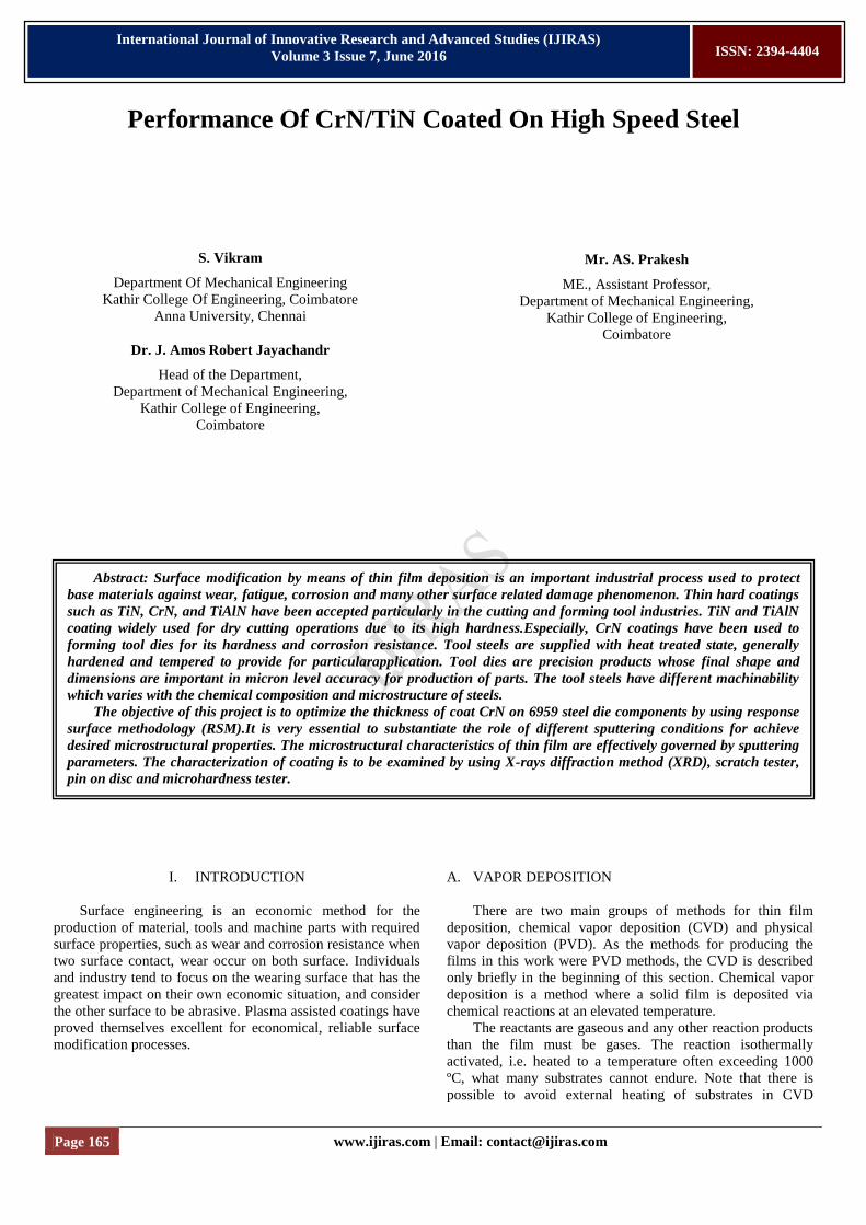
a. PHYSICAL VAPOR DEPOSITION
Physical vapor deposition (PVD) is a concept that gathers
a great number of different deposition methods where the
initial material is in solid phase. And then it is turned into
vapor phase during the process.
A common feature for almost all methods is that they
require a low pressure (vaccum) to avoid impurities in the
film. But also to avoid loss of energy of particles deliberated
from the solid source due to collisions and mainly to keep
enough energy of bombarding particles in sputtering (ions) or
in evaporation (electrons and orions). In PVD the film is
formed when the evaporated or sputtered species condensate
or sublimate on the substrate and all other colder surfaces in
the vacuum chamber. Unlike most of CVD techniques.
PVD processing is carried out in high vaccum at
temperatures between 150 and 500°C. The high-purity, solid
coating material (metals such as titanium, chromium and
aluminium) is either evaporated by heat or by bombardment
with ions (sputtering). At the same time, a reactive gas (e.g.
nitrogen or a gas containing carbon) is forms a compound with
the metal vapour and is deposited on the tools or components
as a thin, highly adherent coating. In order to obtain a uniform
coating thickness, the parts are rotated at uniform speed about
several axes.
Figure 1.1: Physical Vapor Deposition
B. TYPES OF PVD PROCESSES
Cathodic Arc Deposition
Electron beam physical vapor deposition
Evaporative deposition
Pulsed laser deposition
Sputter deposition
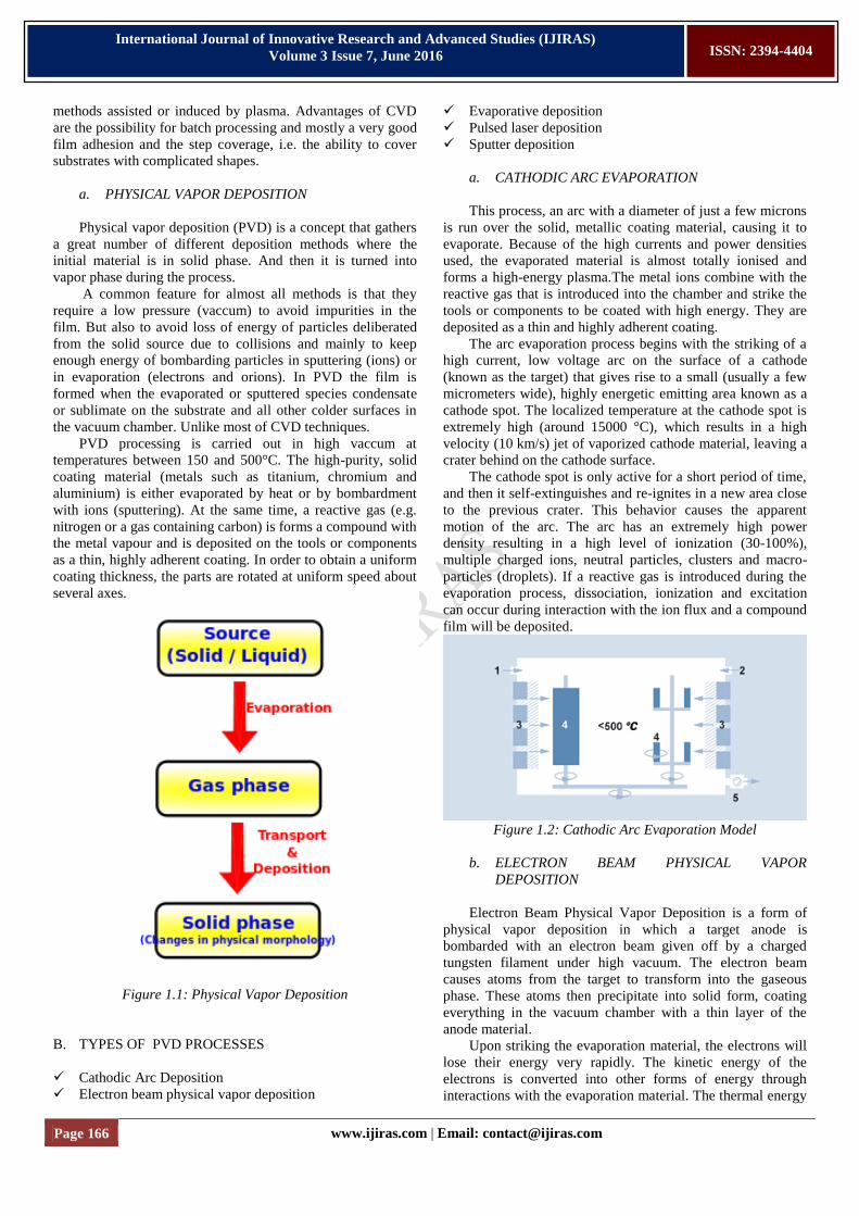
a. CATHODIC ARC EVAPORATION
This process, an arc with a diameter of just a few microns
is run over the solid, metallic coating material, causing it to
evaporate. Because of the high currents and power densities
used, the evaporated material is almost totally ionised and
forms a high-energy plasma.The metal ions combine with the
reactive gas that is introduced into the chamber and strike the
tools or components to be coated with high energy. They are
deposited as a thin and highly adherent coating.
The arc evaporation process begins with the striking of a
high current, low voltage arc on the surface of a cathode
(known as the target) that gives rise to a small (usually a few
micrometers wide), highly energetic emitting area known as a
cathode spot. The localized temperature at the cathode spot is
extremely high (around 15000 °C), which results in a high
velocity (10 km/s) jet of vaporized cathode material, leaving a
crater behind on the cathode surface.
The cathode spot is only active for a short period of time,
and then it self-extinguishes and re-ignites in a new area close
to the previous crater. This behavior causes the apparent
motion of the arc. The arc has an extremely high power
density resulting in a high level of ionization (30-100%),
multiple charged ions, neutral particles, clusters and macro-
particles (droplets). If a reactive gas is introduced during the
evaporation process, dissociation, ionization and excitation
can occur during interaction with the ion flux and a compound
film will be deposited.
Figure 1.2: Cathodic Arc Evaporation Model
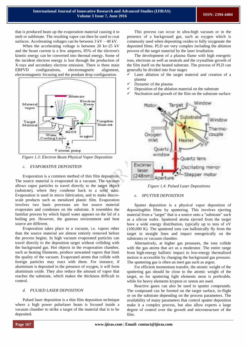
b. ELECTRON BEAM PHYSICAL VAPOR
DEPOSITION
Electron Beam Physical Vapor Deposition is a form of
physical vapor deposition in which a target anode is
bombarded with an electron beam given off by a charged
tungsten filament under high vacuum. The electron beam
causes atoms from the target to transform into the gaseous
phase. These atoms then precipitate into solid form, coating
everything in the vacuum chamber with a thin layer of the
anode material.
Upon striking the evaporation material, the electrons will
lose their energy very rapidly. The kinetic energy of the
electrons is converted into other forms of energy through
interactions with the evaporation material. The thermal energy
Page 167 www.ijiras.com | Email: [email protected]
International Journal of Innovative Research and Advanced Studies (IJIRAS)
Volume 3 Issue 7, June 2016
ISSN: 2394-4404
that is produced heats up the evaporation material causing it to
melt or sublimate. The resulting vapor can then be used to coat
surfaces. Accelerating voltages can be between 3 kV – 40 kV.
When the accelerating voltage is between 20 kv-25 kV
and the beam current is a few amperes, 85% of the electron's
kinetic energy can be converted into thermal energy. Some of
the incident electron energy is lost through the production of
X-rays and secondary electron emission. There is three main
EBPVD configurations, electromagnetic alignment,
electromagnetic focusing and the pendant drop configuration.
Figure 1.3: Electron Beam Physical Vapor Deposition
c. EVAPORATIVE DEPOSITION
Evaporation is a common method of thin film deposition.
The source material is evaporated in a vacuum. The vacuum
allows vapor particles to travel directly to the target object
(substrate), where they condense back to a solid state.
Evaporation is used in micro fabrication, and to make macro-
scale products such as metalized plastic film. Evaporation
involves two basic processes are hot source material
evaporates and condenses on the substrate. It resembles the
familiar process by which liquid water appears on the lid of a
boiling pot. However, the gaseous environment and heat
source are different.
Evaporation takes place in a vacuum, i.e. vapors other
than the source material are almost entirely removed before
the process begins. In high vacuum evaporated particles can
travel directly to the deposition target without colliding with
the background gas. Hot objects in the evaporation chamber,
such as heating filaments, produce unwanted vapors that limit
the quality of the vacuum. Evaporated atoms that collide with
foreign particles may react with them. For instance, if
aluminium is deposited in the presence of oxygen, it will form
aluminium oxide. They also reduce the amount of vapor that
reaches the substrate, which makes the thickness difficult to
control.
d. PULSED LASER DEPOSITION
Pulsed laser deposition is a thin film deposition technique
where a high power pulselaser beam is focused inside a
vacuum chamber to strike a target of the material that is to be
deposited.
This process can occur in ultra-high vacuum or in the
presence of a background gas, such as oxygen which is
commonly used when depositing oxides to fully oxygenate the
deposited films. PLD are very complex including the ablation
process of the target material by the laser irradiation.
The development of a plasma flame with high energetic
ions, electrons as well as neutrals and the crystalline growth of
the film itself on the heated substrate. The process of PLD can
generally be divided into four stages
Laser ablation of the target material and creation of a
plasma
Dynamic of the plasma
Deposition of the ablation material on the substrate
Nucleation and growth of the film on the substrate surface
Figure 1.4: Pulsed Laser Depositions
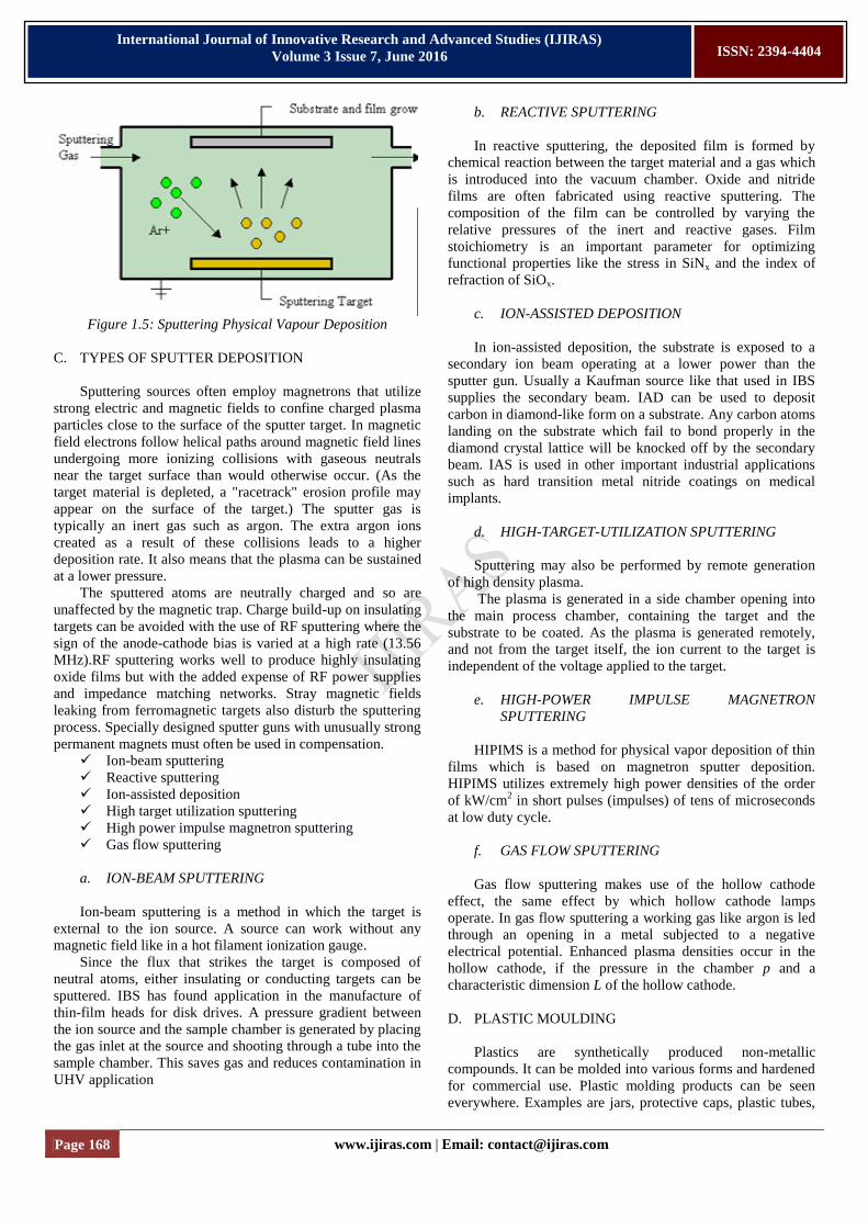
e. SPUTTER DEPOSITION
Sputter deposition is a physical vapor deposition of
depositingthin films by sputtering. This involves ejecting
material from a "target" that is a source onto a "substrate" such
as a silicon wafer. Sputtered atoms ejected from the target
have a wide energy distribution, typically up to tens of eV
(100,000 K). The sputtered ions can ballistically fly from the
target in straight lines and impact energetically on the
substrates or vacuum chamber.
Alternatively, at higher gas pressures, the ions collide
with the gas atoms that act as a moderator. The entire range
from high-energy ballistic impact to low-energy thermalized
motion is accessible by changing the background gas pressure.
The sputtering gas is often an inert gas such as argon.
For efficient momentum transfer, the atomic weight of the
sputtering gas should be close to the atomic weight of the
target, so for sputtering light elements neon is preferable,
while for heavy elements krypton or xenon are used.
Reactive gases can also be used to sputter compounds.
The compound can be formed on the target surface, in-flight
or on the substrate depending on the process parameters. The
availability of many parameters that control sputter deposition
make it a complex process, but also allow experts a large
degree of control over the growth and microstructure of the
film.
Page 168 www.ijiras.com | Email: [email protected]
International Journal of Innovative Research and Advanced Studies (IJIRAS)
Volume 3 Issue 7, June 2016
ISSN: 2394-4404
Figure 1.5: Sputtering Physical Vapour Deposition
C. TYPES OF SPUTTER DEPOSITION
Sputtering sources often employ magnetrons that utilize
strong electric and magnetic fields to confine charged plasma
particles close to the surface of the sputter target. In magnetic
field electrons follow helical paths around magnetic field lines
undergoing more ionizing collisions with gaseous neutrals
near the target surface than would otherwise occur. (As the
target material is depleted, a "racetrack" erosion profile may
appear on the surface of the target.) The sputter gas is
typically an inert gas such as argon. The extra argon ions
created as a result of these collisions leads to a higher
deposition rate. It also means that the plasma can be sustained
at a lower pressure.
The sputtered atoms are neutrally charged and so are
unaffected by the magnetic trap. Charge build-up on insulating
targets can be avoided with the use of RF sputtering where the
sign of the anode-cathode bias is varied at a high rate (13.56
MHz).RF sputtering works well to produce highly insulating
oxide films but with the added expense of RF power supplies
and impedance matching networks. Stray magnetic fields
leaking from ferromagnetic targets also disturb the sputtering
process. Specially designed sputter guns with unusually strong
permanent magnets must often be used in compensation.
Ion-beam sputtering
Reactive sputtering
Ion-assisted deposition
High target utilization sputtering
High power impulse magnetron sputtering
Gas flow sputtering
a. ION-BEAM SPUTTERING
Ion-beam sputtering is a method in which the target is
external to the ion source. A source can work without any
magnetic field like in a hot filament ionization gauge.
Since the flux that strikes the target is composed of
neutral atoms, either insulating or conducting targets can be
sputtered. IBS has found application in the manufacture of
thin-film heads for disk drives. A pressure gradient between
the ion source and the sample chamber is generated by placing
the gas inlet at the source and shooting through a tube into the
sample chamber. This saves gas and reduces contamination in
UHV application
b. REACTIVE SPUTTERING
In reactive sputtering, the deposited film is formed by
chemical reaction between the target material and a gas which
is introduced into the vacuum chamber. Oxide and nitride
films are often fabricated using reactive sputtering. The
composition of the film can be controlled by varying the
relative pressures of the inert and reactive gases. Film
stoichiometry is an important parameter for optimizing
functional properties like the stress in SiNx and the index of
refraction of SiOx.
c. ION-ASSISTED DEPOSITION
In ion-assisted deposition, the substrate is exposed to a
secondary ion beam operating at a lower power than the
sputter gun. Usually a Kaufman source like that used in IBS
supplies the secondary beam. IAD can be used to deposit
carbon in diamond-like form on a substrate. Any carbon atoms
landing on the substrate which fail to bond properly in the
diamond crystal lattice will be knocked off by the secondary
beam. IAS is used in other important industrial applications
such as hard transition metal nitride coatings on medical
implants.
d. HIGH-TARGET-UTILIZATION SPUTTERING
Sputtering may also be performed by remote generation
of high density plasma.
The plasma is generated in a side chamber opening into
the main process chamber, containing the target and the
substrate to be coated. As the plasma is generated remotely,
and not from the target itself, the ion current to the target is
independent of the voltage applied to the target.
e. HIGH-POWER IMPULSE MAGNETRON
SPUTTERING
HIPIMS is a method for physical vapor deposition of thin
films which is based on magnetron sputter deposition.
HIPIMS utilizes extremely high power densities of the order
of kW/cm2 in short pulses (impulses) of tens of microseconds
at low duty cycle.
f. GAS FLOW SPUTTERING
Gas flow sputtering makes use of the hollow cathode
effect, the same effect by which hollow cathode lamps
operate. In gas flow sputtering a working gas like argon is led
through an opening in a metal subjected to a negative
electrical potential. Enhanced plasma densities occur in the
hollow cathode, if the pressure in the chamber p and a
characteristic dimension L of the hollow cathode.
D. PLASTIC MOULDING
Plastics are synthetically produced non-metallic
compounds. It can be molded into various forms and hardened
for commercial use. Plastic molding products can be seen
everywhere. Examples are jars, protective caps, plastic tubes,
Page 169 www.ijiras.com | Email: [email protected]
International Journal of Innovative Research and Advanced Studies (IJIRAS)
Volume 3 Issue 7, June 2016
ISSN: 2394-4404
grips, toys, bottles, cases, accessories, kitchen utensils and a
lot more. The basic idea in plastic molding is inserting molten
liquid plastic into a ready shaped mold. For example the mold
of a bottle. It will be then allowed to cool, and then the mold
will be removed to reveal the plastic bottle. Plastic molding
can also custom-mold a wide variety of plastic products such
as garden pots, cabinets, office trays and boxes, barriers,
barricades and traffic signage etc.
E. TYPES OF PLASTIC MOULDING
a. INJECTION MOULDING
In Injection Moulding, melted plastic is forced into a
mold cavity. Once cooled, the part can be removed. This
plastic moulding process is commonly used in mass-
production or prototyping of a product. These can be used for
production of toys, kitchen utensils, and cell phone stands to
name a few.
b. BLOW MOULDING
Blow moulding is like injection moulding except that hot
liquid plastic pours out of a barrel vertically in a molten tube.
The mold closes on it and forces it outward to conform to the
inside shape of the mold. When it is cooled, the hollow part is
formed.
Examples of blow moulding products are bottles, tubes
and containers. Equipment needed in setting-up a blow
molding business is relatively higher than injection molding.
c. COMPRESSION MOULDING
In this type of plastic moulding, a slug of hard plastic is
pressed between two heated mold halves. Compression
molding usually uses vertical presses instead of the horizontal
presses used for injection and blow moulding. The parts
formed are then air-cooled. Prices of equipment used for
compression moulding are moderate.
d. FILM INSERT MOULDING
This plastic moulding technique imbeds an image beneath
the surface of a molded part. A material like film or fabric is
inserted into a mold. Plastic is then injected.
e. GAS ASSIST MOULDING
Gas injection moulding is used to create plastic parts with
hollow interiors. Partial shot of plastic is then followed by
high-pressure gas to fill the mold cavity with plastic.
f. ROTATIONAL MOULDING
Hollow molds packed with powdered plastic are secured
to pipe-like spokes that extend from a central hub. The molds
rotate on separate axes at once. The hub swings the whole
mold to a closed furnace room causing the powder to melt and
stick to the insides of the tools. As the molds turn slowly, the
tools move into a cooling room.
Here, sprayed water causes the plastic to harden into a
hollow part. In this type of plastic moulding, tooling costs are
low and piece prices are high. Cycle time takes about 40-45
minutes.
g. STRUCTURAL FOAM MOULDING
Structural foam molding is a process of plastic molding
usually used for parts that require thicker walls than standard
injection molding. Inserting a small amount of nitrogen or
chemical blow agent into the plastic material makes the walls
thicker. Foaming happens as the melted plastic material enters
the mold cavity. This type of plastic molding can be used with
any thermoplastic that can be injection molded.
h. THERMOFORMING
In this plastic molding process, sheets of pre-extruded
rigid plastics are horizontally heated and sucked down into
hollow one-piece tools. When the hot plastic solidifies, its
shape conforms to that of the mold.
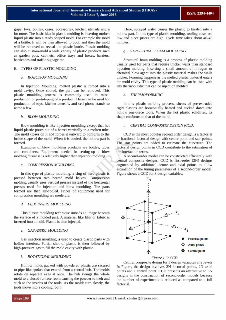
i. CENTRAL COMPOSITE DESIGN (CCD)
CCD is the most popular second order design is a factorial
or fractional factorial design with centre point and star points.
The star points are added to estimate the curvature. The
factorial design points in CCD contribute to the estimation of
the interaction terms.
A second-order model can be constructed efficiently with
central composite designs. CCD is first-order (2N) designs
augmented by additional centre and axial points to allow
estimation of the tuning parameters of a second-order model.
Figure shows a CCD for 3 design variables.
Figure 1.6: CCD
Central composite design for 3 design variables at 2 levels
In Figure, the design involves 2N factorial points, 2N axial
points and 1 central point. CCD presents an alternative to 3N
designs in the construction of second-order models because
the number of experiments is reduced as compared to a full
factorial.
Page 170 www.ijiras.com | Email: [email protected]
International Journal of Innovative Research and Advanced Studies (IJIRAS)
Volume 3 Issue 7, June 2016
ISSN: 2394-4404
II. LITERATURE REVIEW
A. “MICROSTRUCTURAL CHARACTERIZATIONS
AND HARDNESS EVALUATION OF D.C. REACTIVE
MAGNETRON SPUTTERED CRN THIN FILMS ON
STAINLESS STEEL SUBSTRATE” BY HETAL N
SHAH ET AL., BULL IN MATER. SCI., VOL. 33, NO.
2, APRIL 2010, PP. 103–110. © INDIAN ACADEMY
OF SCIENCES.
Investigate the microstructural characterization of CrN
coating on stainless steels as a function of substrate
temperature, working pressure and power. At low working
pressure residual stress buildup on the thin film. Deposition
rate is decreased with increase in working pressure due to
decrease in MFP. The stress induced in the film decrease
within increase in pressure.
Microhardness of thin film decreases with increase of
pressure. It is because of presence of crystal imperfection in
film growth. Low temperature causes residual stress which
leads to poor adhesion between film and substrate. The
microhardness of thin film is increased with increase in
temperature due to grain refinement. The mobility of atoms
leads to more perfect structure. This leads to reduction in grain
size which increases the minimum stress required to activate
the dislocation.
B. “CORROSION OF STAINLESS STEEL COATED
WITH TIN, (TiAl) N AND CrN IN AQUEOUS
ENVIRONMENTS” BY M.A.M.IBRAHIM, S.F.
KORABLOV AND M.YOSHIMURA IN CORROSION
SCIENCE 44 (2002) 815-828.
The corrosion behavior of TiN and CrN coated on M2
HSS by physical vapor deposition was examined in 8 M NaCl
solution. The study was performed using open circuit
potential, potentiodynamic polarization and cyclic polarization
techniques, complemented with XRD and laser microscopy.
However they are prone to corrosive attack as consequence of
the presence of microstructure defects such as pinholes and
pores.
C. “CHARACTERIZATION OF LOW TEMPERATURE
CRN AND TIN (PVD) HARD COATINGS‟‟ BY B.
NAVINSEK, P. PANJAN, A. CVELBAR IN ELSEVIER
SURFACE AND COATINGS TECHNOLOGY 74 – 75
(1995) 155-161.
The plasma beam sputtering process was used to prepare
CrN and TiN hard coatings on steel, sapphire and alumina
Superstrate substrates at a temperature of 200°C. The
microstructural characteristics, coating morphology,
interfacial properties, microhardness and internal stresses were
studied for coatings 3 µm thick. Their oxidation behaviour in
an oxygen flow in a tube furnace wasstudied at temperatures
up to 600°C for TiN and up to 800°C for CrN coatings.
The initial stage of oxidation of TiN and CrN coatings
350 nm thick was also studied by continuous electrical
resistivity measurements. This measurement technique offers
high reproducibility and accuracy, so can be used to study
oxidation for all types of hard coating, and especially for new
multilayer and duplex coatings. Weight gain measurements
and Auger electron spectroscopy depth profile analyses of
oxidized stoichiometric CrN coatings showed that oxidation in
an oxygen flow at 800°C for 4 h induced the growth of a
stable Cr2O3 film.
The thickness of this oxide film was only 15% of the total
(3 µm) coating thickness. The surface morphology and small
roughness changes - as also observed after a long-term test at
800 °C for 200 h in oxygen - indicated that a stoichiometric
CrN coating with the measured properties can be successfully.
D. “OPTIMIZATION OF NITRIDED CASE STRUCTURE
IN COMPOSITE LAYERS CREATED BY DUPLEX
TREATMENT ON THE BASIS OF PVD COATING
ADHESION MEASUREMENT” BY J.WALKOWICZ,
J.SMOLIK, J. TACIKOWSKIIN SURFACE AND
COATINGS TECHNOLOGY 116–119 (1999) 370–379.
The paper concerns the process of the composite:
„nitrided layer-PAPVD coating‟ creation on substrates made
of hot working steel. The composite properties are determined
by the appropriate selection of coating parameters and nitrided
case structure. The results of research concerning the influence
of a method of substrate nitriding and the created nitrided case
structure on the adhesion and plastic properties of the PAPVD
coatings are presented in the paper. Substrates made of hot
working steel EN X35CrMoV5 (0.4% C, 0.4% Mn, 1.0% Si,
5.0% Cr, 1.3% Mo, 0.3% V) underwent different processes of
thermo-chemical and finishing surface treatment in order to
obtain a nitrided layer of a different structure: Fea(N),
Fea(N)+„white layer‟-e,c¾.
Research was carried out for nitrided layers created in a
controlled gas nitriding process. Four different coatings of
nitrides, TiN, Ti(C,N), CrN, (Ti,Cr)N, were deposited on
substrates with nitrided layers using the arc-vacuum method
and the MZ-383 equipment manufactured by Metaplas Ion.
Thanks to an appropriately selected coating material (e.g.
CrN), it is possible to create the composite nitrided layer
(Fea(N)+„white layer‟ e and c¾)+PAPVD coating. This is
important for composites, where the nitrided layer is created
together with the „white layer‟ of iron nitrides e and c¾ on the
surface. The feasibility of in-process structuring for producing
controllable thin film morphologies with features suitable for
the modification of tribological properties was indicated.. The
coarser surface structures seem to act as lubricant reservoirs
and wear debris traps, in contrast to surfaces that do not
contain sufficient pores and crevices.
E. “IN-PROCESS STRUCTURING OF CRN COATINGS,
AND ITS INFLUENCE ON FRICTION IN DRY AND
LUBRICATED SLIDING” BY S. ORTMANN ET AL.,
IN JOURNAL OF MATERIALS PROCESSING
TECHNOLOGY 187–188 (2007) 566–570.
In this study, CrN coatings deposited by plasma-activated
physical vapor deposition (PAPVD) on hard metal substrates
were structured by variation of the deposition parameters that
were varied. In this study, the bias voltage was determined to
have the greatest influence on the surface structure of the
Page 171 www.ijiras.com | Email: [email protected]
International Journal of Innovative Research and Advanced Studies (IJIRAS)
Volume 3 Issue 7, June 2016
ISSN: 2394-4404
coatings. A wide variety of structures ranging from only
somewhat creviced to highly creviced were fabricated, with
grain sizes ranging from 5 to 500 nm.
The feasibility of in-process structuring for producing
controllable thin film morphologies with features suitable for
the modification of tribological properties was indicated. In
ball-on-disk tests run under conditions of minimal, single-
application lubrication with mineral oil, the highly textured
surfaces with larger, well-defined grains and crevices showed
better sliding wear endurance and lower friction coefficients
than smoother, denser surfaces. The coarser surface structures
seem to act as lubricant reservoirs and wear debris traps, in
contrast to surfaces that do not contain sufficient pores and
crevices.
F. “SUBSTRATE DEPENDENCE OF THE SCRATCH
RESISTANCE OF CRNX COATINGS ON STEEL” BY
J.-D. KAMMINGA ET AL., BYK.-D.BOUZAKIS, G.
SKORDARISA, E. BOUZAKISA,B,
A.TSOUKNIDASA, S. MAKRIMALLAKISA, S.
GERARDISA, G. KATIRTZOGLOUA, IN
MANUFACTURING TECHNOLOGY 60 (2011) 587–
590.
In this paper, the effect of substrate hardness on the
scratch test performance is explored. CrNx hard coatings
sputter deposited under various nitrogen flows on two
different steel types were subjected to scratch testing. Two
different failure mechanisms that occurred, i.e. coating
chipping and complete coating removal, were investigated.
The critical loads for chipping and complete coating removal
are higher for coatings deposited on the harder steel.
Substrate independent measures for the onset of failure
are obtained if critical track widths are considered instead of
critical loads. The composite scratch hardness can be written
as the product of the track width independent substrate scratch
hardness and a track width dependent function b(w) that
depends on the coating properties, but that is substrate
independent. The volume law of mixtures model by Burnett
and Rickerby, originally intended to describe the composite
Vickers hardness cannot be used for the scratch hardness.
Upon loading a coated specimen in the scratch test, the
hardening of the specimen due to the presence of the coating
increases with increasing load until chipping of the coating
occurs.
G. “CRN/ALN SUPERLATTICE COATINGS
SYNTHESIZED BY PULSED CLOSED FIELD
UNBALANCED MAGNETRON SPUTTERING WITH
DIFFERENT CRN LAYER THICKNESSES”BY
JIANLIANG LIN ET AL., IN APPLIED SURFACE
SCIENCE 255 (2008) 1865–1869.
In this study the influence of coating thickness on
microstructural characteristics of CrN/AlN super lattice
coating was investigated. CrN/AlN super lattice coatings with
different CrN layer thicknesses were synthesized in a pulsed
closed field unbalanced magnetron sputtering system by
varying the Cr target powers, while keeping the Al target
power and the settle periods of the substrate in front of the
targets constantly.
It was found that the bilayer period (CrN layer thickness)
was decreased almost linearly with a simultaneously increase
in the Al/ (Cr+Al) ratios in the coatings The decrease in the
CrN layer thickness led to a decrease in the lattice parameter
and the residual stress, which are possibly due to the increased
Al content and the number of the interfaces in the coatings
H. “EFFECT OF COATING THICKNESS AND
DEPOSITION METHODS ON THE STRIPPING RATE
OF CR–N COATINGS” BY J.C. AVELAR-BATISTA
ET AL., IN MATERIAL SCIENCE (235-242).
In this work, Cr–N coatings deposited by magnetron
sputtering, arc and electron beam evaporation, having different
thicknesses, were wet-stripped. The stripping rate was
evaluated by statistical analyses for each deposition method
and thickness. Moreover, the stripping rate was not influenced
by changes in the coating structure with increased thickness,
which occurred in arc and electron beam Cr–N coatings.
The highest stripping rate recorded for magnetron Cr–N
coatings could not be explained by changes in coating
structure/morphology and surface roughness. The differences
in the stripping were attributed to the amount of CrN phase
present in the coatings.
I. “INFLUENCE OF NITROGEN FLOW RATES ON
MATERIALS PROPERTIES OF CRNX FILMS
GROWN BY REACTIVE MAGNETRON
SPUTTERING” BY B SUBRAMANIAN ET AL., IN
MEASUREMENT 50 (2014) 19–28.
They Investigated influence of nitrogen flow rates on the
materials properties of reactive magnetron sputtered
chromium nitride (CrNx) thin films. They finalized that grain
size increases with the increase in the nitrogen flow rate. The
CrN films deposited at low nitrogen flow rate showed that the
electrical resistivity correspond to a metallic-like behavior and
the films prepared at higher Nitrogen flow rate and above
showed a semiconducting behavior.
Increase in nitrogen flow rate increases the grain size.
This is due to MFP of particles are shorter and they decrease
with increase in nitrogen flow rate. At low nitrogen flow pure
CrN phase exist.
III. METHODOLOGY
A. SELECTION OF TOOL STEEL
The tool steels used for plastic or rubber moulds normally
classified or supplied with a) Pre-hardened steels b) annealed
steels c) age hardening steels
a. PRE-HARDENED STEELS
The pre-hardened steels are supplied in hardened and
tempered condition. Then straightly goes to production
processes with no need of immediate heat treatment processes.

Page 172 www.ijiras.com | Email: [email protected]
International Journal of Innovative Research and Advanced Studies (IJIRAS)
Volume 3 Issue 7, June 2016
ISSN: 2394-4404
ADVANTAGE
Less time in manufacturing cycle.
No cracking during heat treatment.
DISADVANTAGE
The machining requires more time than annealed steel
which has lower hardness.
b. ANNEALED STEELS
Theses steels can be put into production only after a
further heat treatment since these are supplied in low hardness
values. The manufacturing cycle of these steels are
ADVANTAGE
Short machining time due to annealed condition.
DISADVANTAGE
Occurrence of crack during heat treatment.
c. AGE HARDENING STEELS
They are supplied with solution condition with a hardness
value similar to pre- hardened steels that can be further
increased by heat treatment. The steels used for plastic moulds
are SS420, high-speed steels, cast iron. The composition and
properties of these steels are shown in table.
S.No Material Composition
C Mn Si Cr Mo Ni
1 SS420 0.15 1 1 12-14 - -
2
High-
Speed
Steel
0.35 0.75 0.3 1.5 0.65 3.5
3 Cast Iron 0.25-
0.30 1.6 0.4 2.10 0.25 1.2
Table 3.1: Composition of various Tool Steels
S.No Material
Modulus
of
elasticity
(Gpa)
Thermal
expansion(2
0ºC) x 10-6/
ºC
Thermalc
onductivit
y(W/mºk)
Hardne
ss
(HRc)
1 SS420 205 12.8 29 52
2 High- 210 13.4 24.7 30-42
Speed
Steel
3 CAST IRON
180 11.6 34 29-33
Table 3.2: Properties of Tool Steels
B. COATING MATERIAL
a. DEPOSITION MATERIAL [CrN]
CrN coating is conventionally used for more hardness and
high corrosion resistance industrial applications. The good
sliding behaviour of the coating protects against at deficient
lubrication. Compared with hard chromium plating, CrN
similar corrosion resistance but significantly higher hardness
and better coating adhesion. For coating CrN in DC
Magnetron sputtering Deposition 99.99 % of pure chromium
target was selected.
b. CHARACTERISTICS OF CRN COATING
The coated metal is hard and extremely resistant abrasion.
It has High Corrosion resistance and surface finish.
CrN has higher oxidation temperature (700 ºC) than TiN.
CrN has relatively higher thermal stability, low deposition
temperature, superior wear and corrosion resistance than
TiN.
c. APPLICATION
Metal cutting application
Die product
Oil expellers, pulleys
Conveyor, Screws
Decorative applications
d. DEPOSITION MATERIAL [TiN]
Thin film diffusion barriers are required in semiconductor
devices to prevent the migration of metalatoms from the
interconnects into the adjacent dielectric and semiconductor
regions. Titanium nitride (TiN)is one of the most widely used
diffusion barrier materials.
TiN is a hard, refractory material and has a bulk
resistivity. The shrinking of device dimensions demands
thinner diffusion barrier films deposited in higher aspect ratio
contact holes and vias.
Physical vapour deposition can be an ideal technique for
growing conformal films on high aspect ratio structures. PVD
utilizes two sequential self-limiting reactions that occur
between a gaseous precursor and the solid substrate.
e. CHARACTERISTICS OF TIN COATING
TiN has lower oxidation temperature (600 ºC) than CrN.
TiN has relatively higher thermal stability, low deposition
temperature, superior wear and corrosion resistance than
TiN.
TiN is the most popular coating so far in the past year.
Have proven their effectiveness to increase tool life.
Page 173 www.ijiras.com | Email: [email protected]
International Journal of Innovative Research and Advanced Studies (IJIRAS)
Volume 3 Issue 7, June 2016
ISSN: 2394-4404
f. APPLICATION
Have proven their effectiveness to increase tool life
Plastic formation
Die product
Metal cutting
Decorative application
IV. DESIGN PROCEDURE
A. DESIGNS WITH DIMENSION
In this project application is to make a material with high
resistance heat, wear and corrosion resistance. So that, my
machining tool is having three- coordinates (x, y and z). In
that I have concentrating single dimension and also
specifically calling as name of specimen. The specimen
dimension is 10 x 40 mm.
Figure 4.1: Sketch of Three Dimension Design
V. EXPERIMENTAL PROCEDURE
A. SPECIMEN PREPARATION
The specimens are prepared from the M2 grade high
speed steel.
Parts are cleaned in a multi-stage cleaning process to
remove soils, oils, fingerprints and produce an oxide free
surface.
The specimens are cleaned on the stage of ultrasonic
effect for Removing oil and other contamination and
liquid honing for surface roughness by using fine
adhesive powder.
The surface of specimens has been coated by using PVD
techniques.
The thickness of coated surface layer is existing between
3 micrometer.
The CrN/TiN has been used for surface coating material
on substrate by PVD method.
The specimens have been prepared for dimensions of 10 x
40mm.
The surface of specimens has been hard coated CrN/TiN
by DC Magnetron sputtering deposition process.
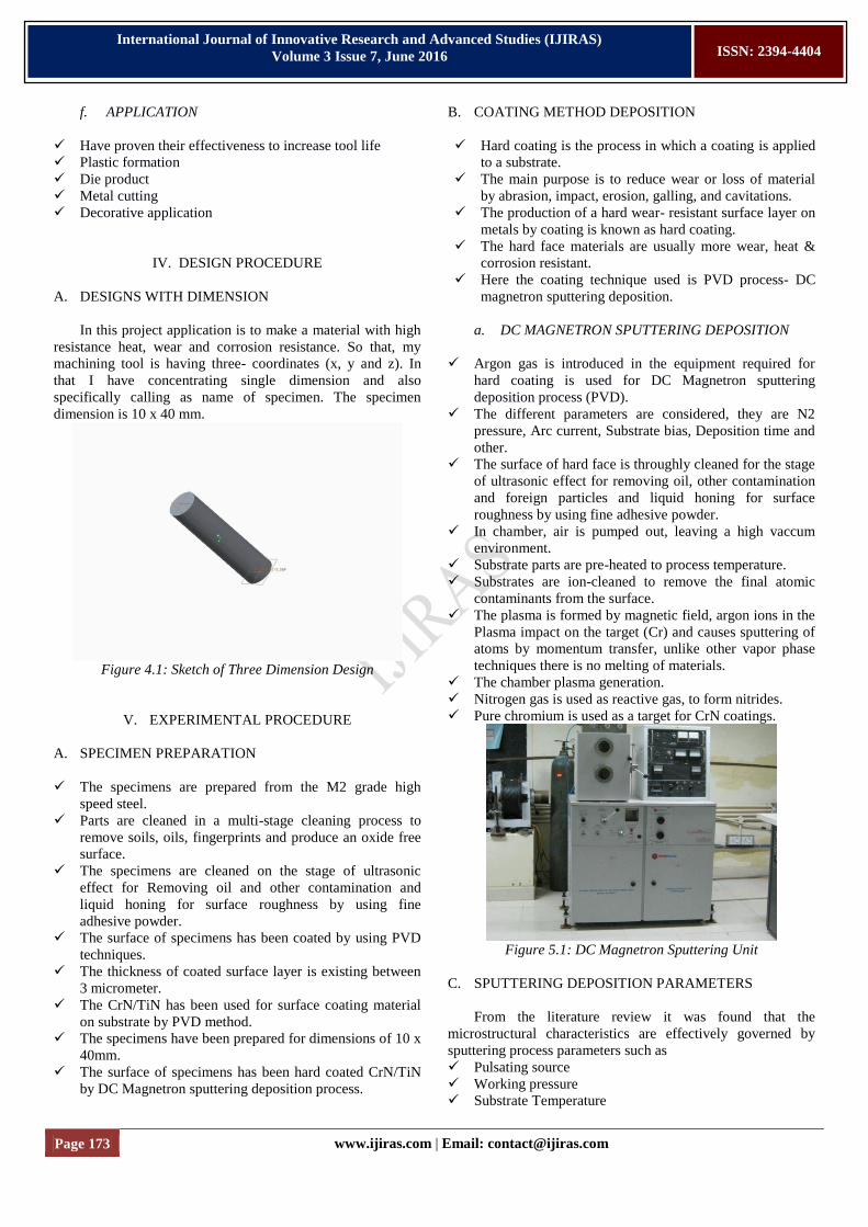
B. COATING METHOD DEPOSITION
Hard coating is the process in which a coating is applied
to a substrate.
The main purpose is to reduce wear or loss of material
by abrasion, impact, erosion, galling, and cavitations.
The production of a hard wear- resistant surface layer on
metals by coating is known as hard coating.
The hard face materials are usually more wear, heat &
corrosion resistant.
Here the coating technique used is PVD process- DC
magnetron sputtering deposition.
a. DC MAGNETRON SPUTTERING DEPOSITION
Argon gas is introduced in the equipment required for
hard coating is used for DC Magnetron sputtering
deposition process (PVD).
The different parameters are considered, they are N2
pressure, Arc current, Substrate bias, Deposition time and
other.
The surface of hard face is throughly cleaned for the stage
of ultrasonic effect for removing oil, other contamination
and foreign particles and liquid honing for surface
roughness by using fine adhesive powder.
In chamber, air is pumped out, leaving a high vaccum
environment.
Substrate parts are pre-heated to process temperature.
Substrates are ion-cleaned to remove the final atomic
contaminants from the surface.
The plasma is formed by magnetic field, argon ions in the
Plasma impact on the target (Cr) and causes sputtering of
atoms by momentum transfer, unlike other vapor phase
techniques there is no melting of materials.
The chamber plasma generation.
Nitrogen gas is used as reactive gas, to form nitrides.
Pure chromium is used as a target for CrN coatings.
Figure 5.1: DC Magnetron Sputtering Unit
C. SPUTTERING DEPOSITION PARAMETERS
From the literature review it was found that the
microstructural characteristics are effectively governed by
sputtering process parameters such as
Pulsating source
Working pressure
Substrate Temperature
Page 174 www.ijiras.com | Email: [email protected]
International Journal of Innovative Research and Advanced Studies (IJIRAS)
Volume 3 Issue 7, June 2016
ISSN: 2394-4404
Target to substrate distance
Reactive gas flow rate
Deposition time
Target power
D. EFFECT OF PROCESS PARAMETERS
a. EFFECT OF WORKING PRESSURE
At low working pressure residual stress buildup on the
thin film.
Deposition rate is decreased with increase in working
pressure due to decrease in MFP (Mean Free Path).
The stress induced in the film decrease within increase in
pressure. Because the reduction in energies of plasma
particles due to inelasticscattering.
b. EFFECT OF TEMPERATURE
The oxidation of CrN/TiN thin films occurs around 700°C
and Low temperature causes residual stress which leads to
poor adhesion between film and substrate.
The microhardness of thin film is increased with increase
in temperature due to grain refinement. The mobility of
atoms leads to more perfect structure.
This leads to reduction in grain size which increases the
minimum stress required to activate the dislocation.
c. EFFECT OF REACTIVE GAS (NITROGEN) FLOW
RATE
Increase in nitrogen flow rate increases the grain size and
at low nitrogen flow pure CrN/TiN phase exist.
While increasing flow rate the percentage of pure
CrN/TiN phase will decrease and due to rapid
solidification of highly energetic particles.
The electrical resistivity of film is increased with increase
in nitrogen flow rate because of increase in impurity
defect.
d. EFFECT OF DEPOSITION RATE
The deposition rate decreases with increasing working
pressure.
It influences the crystallinity, texture and porosity of the
film.
VI. EXPERIMENTAL RESULTS
The following various tests are taken to compare the CrN
and TiN coatings on high speed steel.
Chemical composition test
Corrosion test
Wear test
XRD (X-ray diffraction)
SEM
EDAX
A. X-RAY DIFFRACTION (XRD)
a. EXPERIMENTAL PROCEDURE
When you have finished please remember to remove your
sample and close the enclosure doors.
Do not store your materials, samples, or sample holders in
the XRD room.
You are welcome to use the department sample holders
provided you don‟t remove them from the lab and that
you clean them when you have finished.
Do not close XRD commander. This would prevent the
machine from returning to stand-by mode and can reduce
the life of the XRD tube.
If you sign-up for time on the machine and cannot make it
for any reason, please contact the SIT so your name can
be removed from the scheduler.
If you need to run a scan that will take more than 2 hours,
please notify the SIT and we will arrange for an overnight
scan.
b. XRD RESULT FOR CrN
Position [°2Theta] (Copper (Cu))
20 30 40 50 60 70 80
Counts
0
20
40
60 CrN
Figure 6.1: XRD Result for CrN
Peak List Pos.
[°2Th.]
Height
[cts]
FWHM Left
[°2Th.]
d-spacing
[Å]
Rel. Int.
[%]
30.8565 2.97 0.4920 2.89792 7.26
43.4453 17.41 0.4920 2.08297 42.60
45.5398 7.93 0.2952 1.99193 19.41
64.2132 10.05 0.5904 1.45050 24.59
67.9814 40.86 0.5904 1.37899 100.00
Table 6.1: XRD Result for CrN
c. XRD RESULT FOR TiN
Position [°2Theta] (Copper (Cu))
20 30 40 50 60 70 80
Counts
0
200
400
TiN
Figure 6.1: XRD Result For TiN
Page 175 www.ijiras.com | Email: [email protected]
International Journal of Innovative Research and Advanced Studies (IJIRAS)
Volume 3 Issue 7, June 2016
ISSN: 2394-4404
PEAK LIST Pos.
[°2Th.]
Height
[cts]
FWHM Left
[°2Th.]
d-spacing
[Å]
Rel. Int.
[%]
10.7793 6.23 1.1808 8.20771 1.30
36.6703 53.38 0.5904 2.45073 11.17
40.1555 29.72 0.2952 2.24570 6.22
42.7566 89.06 0.1968 2.11491 18.64
44.8753 477.68 0.1968 2.01986 100.00
65.1683 47.85 0.2952 1.43154 10.02
72.7115 19.60 0.5904 1.30051 4.10
Table 6.1: XRD Result for TiN
B. CHEMICAL COMPOSITION TEST
a. EXPERIMENTAL PROCEDURE
Initially the optical emission spectrometer is arranged for
testing the materials such as high speed steel, high speed
steel with chromium nitrate coated, high speed steel with
titanium nitrate coated as manner.
The materials are holded to test the chemical composition
and as well as the power supply is to it.
When the power supply is given, the spark is produced on
the testing materials such as HSS, HSS with CrN coated
and HSS with TiN coated.
Finally the tested materials are removed from the optical
emission spectrometer as well as power supply is
switched off.
COMPOSITION
PERCENTAGE
HSS CrN TiN
Carbon 0.771% 0.873% 0.869%
Manganese 0.278% 0.291% 0.274%
Silicon 0.384% 0.373% 0.366%
Sulphur 0.030% 0.032% 0.030%
Chromium 3.912% 4.052% 3.883%
Molybdenum 4.741% 4.958% 5.213%
Nickel 0.191% 0.192% 0.201%
Cobalt 1.323% 1.377% 1.411%
Vanadium 1.948% 2.133% 2.076%
Tungsten 6.425% 6.398% 6.850%
Iron Remainder (79.9955%)
Remainder (79.319%)
Remainder (78.826%)
Table 6.2: Chemical Composition Test
C. CORROSION TEST
a. EXPERIMENTAL PROCEDURE
Initially 350 ml of double distilled water is taken into the
beaker. And 8gm of NaCl is added and it‟s fully mixed
into the water.
The corrosion measuring unit knobs are connected and
picked with the testing piece, secondary electrode
(graphite) and glass electrode.
The power supply is given to the equipment.
When the power supply is given, the graphite act as a
counter electrode and testing material act as a working
electrode.
The required both the anodic and cathodic voltages are
settled.
At starting the corrosion behaviour waits till completion
of ionic equalization process.
After the equalization process, the corrosion action takes
place on high speed steel.
b. CORROSION RATE ANALYSIS
Log(Current /A)
Po
ten
tial
Corrosion rate analysis
-6 -5 -4 -3 -2 -1
A
-0.6
-0.5
-0.4
-0.3
-0.2
Figure 6.3: Corrosion Rate for HSS
Log(Current /A)
Pote
ntial
Corrosion rate analysis
-6 -5 -4 -3 -2
A
-0.7
-0.6
-0.5
-0.4
-0.3
V
Figure 6.3: Corrosion Rate for CrN
Log(Current /A)
Po
ten
tial
Corrosion rate analysis
-6 -5 -4 -3 -2
A
-0.6
-0.5
-0.4
-0.3
-0.2
V
Figure 6.3: Corrosion Rate for TiN
Tafel Data
HSS CrN TiN
E. corr V -0.4413 -0.4816 -0.3421
i cor. A 6.888E-5 5.607E-5 3.531E-5
I cor. A/cm^2 6.888E-5 5.607E-5 3.531E-5
Rp Ohm 403.8 643.7 677.2
ba V/dec 0.073 0.097 0.063
bc V/dec 0.525 0.595 0.438
C. Rate mm/y 0.2254 0.1835 0.1155
Table 6.3: Corrosion Test
Page 176 www.ijiras.com | Email: [email protected]
International Journal of Innovative Research and Advanced Studies (IJIRAS)
Volume 3 Issue 7, June 2016
ISSN: 2394-4404
D. WEAR TEST
a. EXPERIMENTAL PROCEDURE
Take care to remove all dirt and foreign matter from the
specimens. Use nonchlorinated, non-film-forming
cleaning agents and solvents
Measure appropriate specimen dimensions to the nearest
2.5 μm or weigh the specimens to the nearest 0.0001 g.
Insert the disk securely in the holding device so that the
disk is fixed perpendicular (61°) to the axis of the
resolution.
Add the proper mass to the system lever or bale to
develop the selected force pressing the pin against the
disk.
Start the motor and adjust the speed to the desired value
while holding the pin specimen out of contact with the
disk. Stop the motor.
Remove the specimens and clean off any loose wear
debris. Note the existence of features on or near the wear
scar such as: protrusions, displaced metal, discoloration,
micro cracking, or spotting.
Remeasure the specimen dimensions to the nearest 2.5 μm
or reweigh the specimens to the nearest 0.0001 g, as
appropriate.
Material Time (s) Wear rate (m)
HSS 511.6340 1212.08
HSS+TiN 511.6340 1138.50
HSS+CrN 511.6340 1103.09
Table 6.4: Wear Test
E. ENERGY DISPERSIVE X-RAY
ANALYSIS(EDXA)TEST
a. EXPERIMENTAL PROCEDURE
Identify the sample name and information for each
adhesive lift in the specimen holder.
Turn on the power and saturate the beam.
Adjust the X-ray dead time on the copper standard to 10
% - 20 %.
Perform instrumental setup of each sample loaded into the
sample stage previously. Include with these samples the
instrument blank and control.
Enter sample description in Analysis, including
Laboratory number and Forensic Scientist‟s name.
Select Perform EDS Check and verify EDS check after
each analysis.
Set the stage point to the copper standard. Use the
backscatter detector and adjust its operational threshold
level.
Start automated analysis.
b. EDXATEST FOR CrN
Figure 6.5: EDXA Test for CrN
Element Weight % Atomic weight %
Cr 94.32 86.04
Fe 1.36 1.15
Table 6.5: EDXA Test for CrN
c. EDXATEST FOR TiN
Figure 6.5: EDXA Test For TiN
Element Weight % Atomic weight %
N 9.06 26.78
Ti 45.23 39.11
Table 6.5: EDXA Test for TiN
F. SCANNING ELECTRON MICROSSCOPE (SEM)TEST
a. EXPERIMENTAL PROCEDURE
Identify the sample name and information for each
adhesive lift in the specimen holder.
Turn on the power and saturate the beam.
Adjust the X-ray dead time on the copper standard to 10
% - 20 %.
Perform instrumental setup of each sample loaded into the
sample stage previously. Include with these samples the
instrument blank and control.
Enter sample description in Analysis, including
Laboratory number and Forensic Scientist‟s name.
Page 177 www.ijiras.com | Email: [email protected]
International Journal of Innovative Research and Advanced Studies (IJIRAS)
Volume 3 Issue 7, June 2016
ISSN: 2394-4404
Select Perform EDS Check and verify EDS check after
each analysis.
Set the stage point to the copper standard. Use the
backscatter detector and adjust its operational threshold
level.
When all settings are correct, select save under Set-Up.
Start automated analysis.
b. SEM TEST FOR CrN
Figure A
Figure B
Figure C
Figure D
c. SEM TEST FOR TiN
Figure A
Figure B
Figure c
Figure D
Page 178 www.ijiras.com | Email: [email protected]
International Journal of Innovative Research and Advanced Studies (IJIRAS)
Volume 3 Issue 7, June 2016
ISSN: 2394-4404
VII. CONCLUSION
It is concluded that M2 grade high speed steel has been
selected as a substrate material because of its moderate
properties of microstructure, chemical composition,
deposition of materials, wear and corrosion rates when
compared and analyzed with other two CrN/TiN coated
high speed steels.
Its purchasing and machining cost is low. So that selected
as a substrate material.
From the literature review it is concluded that the
influencing variables of microstructural characteristics of
CrN coating are substrate temperature, working pressure
and reactive gas flow rate, thickness of the film and
power of sputtering process.
Among the above variables the most influencing variables
of microstructural, corrosion, wear and deposition of materials
characteristics of CrN thin film are substrate temperature,
working pressure and reactive gas flow rate are higher and
more efficient than the other two types of materials such as
HSS and TiN coated HSS.
REFERENCES
[1] A.S.M. Jaya, M.R. Muhammad, M.N.A. Rahman,
Z.A.F.M. Napiah “Hybrid RSM-fuzzy modeling for
hardness prediction of TiAlN coatings”.
[2] B.Subramanian, K Prabakaran and M Jayachandran
“Influence of nitrogen flow rates on materials properties
of CrNx films grown by reactive magnetron sputtering
“Bull. Mater. Sci., Vol. 35, No. 4, August 2012, pp. 505–
511. C Indian Academy of Sciences.
[3] Hetal N Shah, Vipin Chawla, R Jayaganthan and
Davinder Kaur “Microstructural characterizations and
hardness evaluation of d.c.reactive magnetron sputtered
CrN thin films on stainless steel Substrate " Bull. Mater.
Sci., Vol. 33, No. 2, April 2010, pp. 103–110. © Indian
Academy of Sciences.
[4] J.C. Avelar-Batista, E. Spain, J. Housden, G.G. Fuentes ,
R. Rodriguez ,F. Montala, L.J. Carreras , T.J. Tate “Effect
of coating thickness and deposition methods on the
stripping rate of Cr–N coatings “ Surface & Coatings
Technology 200 (2005) 1842 – 1848.
[5] J.-D. Kammingaa, P. van Essena, R. Hoya and G.C.A.M.
Janssen. “Substrate dependence of the scratch resistance
of CrNx coatings on steel “Tribology Letters, Vol. 19,
No. 2, June 2005.
[6] Jianliang Lin , John J. Moore, Brajendra Mishra a, Malki
Pinkas b, Xuhai Zhang a, William D. Sproul c. “CrN/AlN
super lattice coatings synthesized by pulsed closed field
unbalanced magnetron sputtering with different CrN layer
thicknesses” Thin Solid Films 517 (2009) 5798–5804.
[7] M.A.M.Ibrahim, S.F.Korblov, M.yoshimura ”Corrosion
of Stainless Steel coated with TiN, (TiAl) N and CrN in
aqueous Environments “ Corrosion science 44(2002)815-
828.
[8] S. Ortmann, A. Savan, Y. Gerbig, H. Haefke. “In-process
structuring of CrN coatings, and its influence on friction
in dry and lubricated sliding “Wear 254 (2003) 1099–
1105.
[9] Thomas Bjork a, Richard Westergård b, Sture Hogmarkb
“Wear of surface treated dies for aluminium extrusion - a
case study” Wear 249 (2001) 316–323.
[10] Yucong Wang “A study of PVD coatings and die
materials for extended die-casting die life” surface and
coating technology 94-95 (1997).