performance analysis of dwt based ofdm over fft...
TRANSCRIPT
International Journal of VLSI design & Communication Systems (VLSICS) Vol.2, No.3, September 2011
DOI : 10.5121/vlsic.2011.2310 119
Performance analysis of DWT based OFDM over FFT based OFDM and implementing on FPGA
Mrs. VEENA M.B1 & Dr. M.N.SHANMUKHA SWAMY
2
1Research scholar, ECE Department, SJCE, Mysore, Karnataka, India,
2Professor, ECE Department, SJCE, Mysore, Karnataka,India,
[email protected] [email protected]
ABSTRACT
Growth in technology has led to unprecedented demand for high speed architectures for complex signal
processing applications. In 4G wireless communication systems, bandwidth is a precious commodity, and
service providers are continuously met with the challenge of accommodating more users with in a limited
allocated bandwidth. To increase data rate of wireless medium with higher performance, OFDM
(orthogonal frequency division multiplexing) is used. Recently DWT (Discrete wavelet transforms) is
adopted in place of FFT (Fast Fourier transform) for frequency translation. Modulation schemes such as
16-QAM, 32-QAM, 64-QAM and 128-QAM (Quadrature amplitude modulation) have been used in the
developed OFDM system for both DWT and FFT based model. In this paper we propose a DWT-IDWT
based OFDM transmitter and receiver that achieve better performance in terms SNR and BER for AWGN
channel. It proves all the wavelet families better over the IFFT-FFT implementation. The OFDM model is
developed using Simulink, various test cases have been considered to verify its performance. The DWT-
OFDM using Lifting Scheme architecture is implemented on FPGA optimizing hardware, speed & cost.
The wavelet filter used for this is Daubechies (9, 7) with N=2. The RTL code is written in Verilog-HDL
and simulated in Modelsim. The design is then synthesized in Xilinx and implemented on Virtex5 FPGA
board and the results were validated using ChipScope.
Keywords: FFT, DWT, OFDM, BER, Lifting scheme, Simulink
1. INTRODUCTION
A combination of modulation and multiplexing constitutes to Orthogonal Frequency Division
Multiplexing Independent signals that are sub-set of a main signal are multiplexed in OFDM and
also the signal itself is first split into independent channels, modulated by data and then re-
multiplexed to create OFDM carrier. Orthogonality of subcarriers is the main concept in OFDM.
The property of orthogonality allows simultaneous transmission of a lot of sub-carriers in a tight
frequency space without interference from each other. This acts as an undue advantage in OFDM.
Therefore, OFDM is becoming the chosen modulation technique for wireless communication.
International Journal of VLSI design & Communication Systems (VLSICS) Vol.2, No.3, September 2011
120
With the help of OFDM, sufficient robustness can be achieved to provide large data rates to radio
channel impairments. In an OFDM scheme, a large number of orthogonal, overlapping narrow
band sub-channels or sub-carriers transmitted in parallel by dividing the available transmission
bandwidth. Compact spectral utilization with utmost efficiency is achieved with the help of
minimally separated sub-carriers. Main attraction of OFDM lies with how the system handles the
multipath interference at the receiver end.
OFDM is multicarrier modulation (MCM) technique [1] which provides an efficient means to
handle high speed data streams on a multipath fading environment that causes ISI. Normally
OFDM is implemented using FFT and IFFT’s. To decrease the BW waste [4] brought by adding
cyclic prefix, wavelet based OFDM is employed. Due to use of wavelet transform the
transmission power is reduced. The spectral containment of the channels is better since it does not
use cyclic prefix. One type of wavelet transform is Discrete Wavelet transforms have been
considered as alternative platforms for replacing IFFT and FFT. [1],[2],[3]. It employs Low Pass
Filter (LPF) and High Pass Filter (HPF) operating as Quadrature Mirror Filters satisfying perfect
reconstruction and orthonormal properties. The purpose of this paper is to perform the simulation
study of FFT and DWT OFDM systems with respect to BER for AWGN channel for various
modulation schemes. In DWT OFDM system, zero padding and vector transposing is done to
transmit the modulated signal [1]. The DWT has been introduced as a highly efficient and flexible
method for sub band decomposition of signals. The proposed architecture, based on new and fast
lifting scheme approach for (9, 7) filter in DWT, reduces the hardware complexity and memory
accesses. Moreover, it has the ability of performing progressive computations by minimizing the
buffering between the decomposition levels. The architecture has regular structure, simple control
flow, small embedded buffers and low power consumption. Lifting scheme requires fewer
computations so the computational complexity is reduced.
The remainder of the paper is organized as follows. Section 2 explains FFT OFDM & DWT
OFDM model, Section 3 on software reference model, section 4 discusses simulation results for
various modulation and BER for FFT and DWT (Haar) OFDM systems, section 5 on Lifting
based DWT architecture, section 6 on results & discussion, finally the paper is concluded in
section 7.
2. OFDM SYSTEMS
2.1. FFT based OFDM System
An OFDM trans-receiver is shown in Figure (1).The inverse transform block can either be
IDWT/IFFT and forward transform block can be DWT/FFT. The data generator used is a sine
wave of bit stream d. It is processed using QPSK or M-ary QAM modulator to map the input data
into symbols Xm. These symbols are now sent through IFFT block to perform IFFT operation to
generate N parallel data streams. Its output in discrete time domain is given by,
Xk(n)=�
√�∑ ����exp ��2���/� ���
��� ………..………………………….( 1)

International Journal of VLSI design & Communication Systems (VLSICS) Vol.2, No.3, September 2011
121
Figure. 1: An OFDM transceiver with inverse and forward transform blocks for implementation
of FFT/ DWT-OFDM.
The transformed output (Xk) is now appended with cyclic prefix. The cyclic prefix (CP) is added
before transmission, to mitigate ISI effect. It is usually 25% of the last part of the original OFDM
symbol and this data is passed through AWGN channel with proper input power set. At the
receiver, the reverse operation is done to obtain the original data back. The CP is removed and
processed in the FFT block and finally passed through demodulator for data recovery. The output
of the FFT in frequency domain is given by,
Um(i)= ∑������ Uk(n)exp(-j2πni/N)………………………………………….(2)
2.2 DWT based OFDM System
In the trans-receiver model shown in Figure.1, at the transmitter, the input sine wave maps on the
data to modulator (16-QAM), thereby converting data dk into symbols Xmi. Each Xmi is first
converted to serial representation having a vector XX which will next be transposed into CA.
Then, the signal is up-sampled (zero padding) and filtered by the LPF coefficients or
approximated coefficients. Since our aim is to have low frequency signals, the modulated signals
XX perform circular convolution with LPF filter whereas the HPF filter also perform the
convolution with zeroes padding signals CD respectively. Note that the HPF filter contains
detailed coefficients or wavelet coefficients. This data is given as an input to IDWT block
wherein a particular wavelet (Haar) is chosen for simulation and is found to have a better
performance when compared to FFT OFDM. At the receiver, DWT and demodulator (16-QAM)
are used to recover back the data.

International Journal of VLSI design & Communication Systems (VLSICS) Vol.2, No.3, September 2011
122
Fig. 2: DWT Transmitter
At the receiver, DWT and (16-QAM) demodulator are used to recover back the original data as
shown in Figure.3
Figure. 3: DWT Receiver
3. SOFTWARE REFERENCE MODEL
The simulink model for DWT/FFT OFDM system for 64 sub-carriers is shown in figure 4.

International Journal of VLSI design & Communication Systems (VLSICS) Vol.2, No.3, September 2011
Figure. 4: Simulink diagram for DWT/FFT OFDM Systems
4. SIMULATION RESULTS
Simulation parameters:
No. of subcarriers (FFT and DWT): 64
Modulation: 16-QAM
Channel: AWGN
Table 1:BER for various modulation schemes for FFT and DWT OFDM systems of different
wavelets at 20dB SNR
Modulation
scheme
FFT
16-QAM 0.00005499
32-QAM 0.00682600
64-QAM 0.08712000
128-QAM 0.2461000
International Journal of VLSI design & Communication Systems (VLSICS) Vol.2, No.3, September 2011
. 4: Simulink diagram for DWT/FFT OFDM Systems
RESULTS
No. of subcarriers (FFT and DWT): 64
Table 1:BER for various modulation schemes for FFT and DWT OFDM systems of different
Haar Db-3 Db
0.00005499 0.000012 0.9758 0.999
0.00682600 0.003742 0.9994 0.9842
0.08712000 0.060610 0.9992 0.969
0.201000 1.0000 1.000
International Journal of VLSI design & Communication Systems (VLSICS) Vol.2, No.3, September 2011
123
Table 1:BER for various modulation schemes for FFT and DWT OFDM systems of different
Db-4
0.999
0.9842
0.969
1.000

International Journal of VLSI design & Communication Systems (VLSICS) Vol.2, No.3, September 2011
124
Figure. 5: BER plot for 16-QAM FFT/DWT OFDM systems.
From the BER plot above, it is seen that DWT (Haar) outperformed FFT-OFDM system by
nearly 1.5db for 16-QAM modulation scheme for the same BER of 0.001.
5. Lifting based DWT Architecture:
Daubechies (9,7) wavelet filter[11],[13],[15] with N=2 is used for architecture development.
Lifting scheme is used for the development of architecture. Here N=2 means, we will be having
two stages of lifting scheme i.e predict1, update1 and in second stage predict2, update2.The main
feature of the lifting-based wavelet transform is to break-up the high pass and the low pass
wavelet filters into a sequence of smaller filters. The lifting scheme requires fewer computations
so the computational complexity is reduced. The lifting-based wavelet transform basically
consists of three steps, which are called split, lifting, and scaling, respectively, as shown in Figure
6.
Figure 6: The lifting scheme implementation of 1D-DWT [12]
The basic idea of lifting scheme is first to compute a trivial wavelet (or lazy wavelet
transform) by splitting the original 1-D signal into odd and even indexed sub sequences,
International Journal of VLSI design & Communication Systems (VLSICS) Vol.2, No.3, September 2011
125
and then modifying these values using alternating prediction and updating steps. The
lifting scheme algorithm can be described as follow:
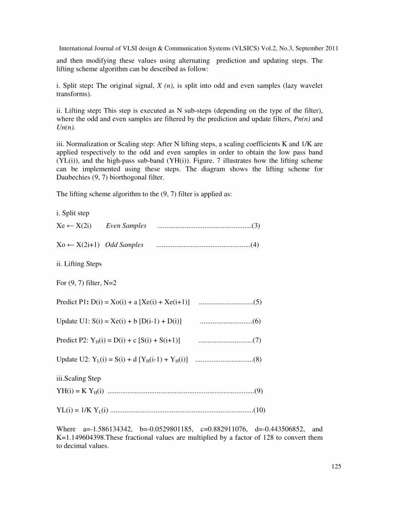
i. Split step: The original signal, X (n), is split into odd and even samples (lazy wavelet
transforms).
ii. Lifting step: This step is executed as N sub-steps (depending on the type of the filter),
where the odd and even samples are filtered by the prediction and update filters, Pn(n) and
Un(n).
iii. Normalization or Scaling step: After N lifting steps, a scaling coefficients K and 1/K are
applied respectively to the odd and even samples in order to obtain the low pass band
(YL(i)), and the high-pass sub-band (YH(i)). Figure. 7 illustrates how the lifting scheme
can be implemented using these steps. The diagram shows the lifting scheme for
Daubechies (9, 7) biorthogonal filter.
The lifting scheme algorithm to the (9, 7) filter is applied as:
i. Split step
Xe ← X(2i) Even Samples ....................................................(3)
Xo ← X(2i+1) Odd Samples ....................................................(4)
ii. Lifting Steps
For (9, 7) filter, N=2
Predict P1: D(i) = Xo(i) + a [Xe(i) + Xe(i+1)] ..............................(5)
Update U1: S(i) = Xe(i) + b [D(i-1) + D(i)] .............................(6)
Predict P2: YH(i) = D(i) + c [S(i) + S(i+1)] ..............................(7)
Update U2: YL(i) = S(i) + d [YH(i-1) + YH(i)] ................................(8)
iii.Scaling Step
YH(i) = K YH(i) .................................................................................(9)
YL(i) = 1/K YL(i) ...............................................................................(10)
Where a=-1.586134342, b=-0.0529801185, c=0.882911076, d=-0.443506852, and
K=1.149604398.These fractional values are multiplied by a factor of 128 to convert them
to decimal values.

International Journal of VLSI design & Communication Systems (VLSICS) Vol.2, No.3, September 2011
126
These mathematical equations can be illustrated by the Figure 7. Another feature of lifting
scheme is that it allows for an inplace computation.
Original Samples Intermediate Samples Final Coefficients
Figure 7: The diagram of 1-D DWT using Lifting Scheme (9,7) filter.[12]
Stage1: In this stage even and odd bits are considered accordingly and equation (5)is computed to
get predict1 output D[i].
Stage 2: The predict1 output (D[i]) along with even position of initial inputs is taken to compute
equation (6) which results in update1 output S[i].
Stage 3: Predict1 (D[i]) and Update1(S[i]) outputs are taken to compute equation(7), which
results in Predict2 output YH[i].
Stage 4: Predict2 (YH[i]) and Update1 (S[i]) outputs are taken to compute equation (8), which
results in Update2 output YL[i].
Just reverse operation of this with corresponding sign change is carried out to compute IDWT.
6. RESULTS & DISCUSSION
6.1 RTL Schematic of the design
Figure 8 shows the RTL schematic of the proposed design with interconnects between the various
blocks. It is a technology independent schematic.

International Journal of VLSI design & Communication Systems (VLSICS) Vol.2, No.3, September 2011
127
Figure 8: RTL Schematic of DWT-IDWT
The top level RTL schematic of the designed lifting scheme based DWT-IDWT architecture is
obtained by the Schematic View tool in Xilinx ISE, which is shown in above figure 8. The netlist
will be generated after synthesis process. This netlist will be saved in Verilog and DDC format
(so that the constraints are embedded in the DDC file). The actual power and the timing were
verified in Primetime. In this design clock period is set as 8ns (means frequency of operation is
125MHz) to meet slack constraint.
6.2 SIMULATION using MODELSIM
In this the lifting scheme based DWT architecture is proposed using (9/7) Db filter and then the
design is modeled using Verilog HDL in structural modeling. Simulation is done using modelsim
and results are analyzed. Synthesis is the transformation of design from higher level of
abstraction to lower level of abstraction. The DWT design using Lifting Scheme is carried out on
Virtex5 FPGA development kit. It is seen that the pre-simulation and post place and route
simulation results match, thereby proving that the design is perfectly mapped onto FPGA meeting
the required design specifications.

International Journal of VLSI design & Communication Systems (VLSICS) Vol.2, No.3, September 2011
128
Figure 9: Simulation result using Modelsim
Figure 10: Outputs of Chip Scope Pro
From Figure 9 it is seen that the simulation results of the proposed architecture modeled in
ModelSim matches with the results from Chip scope Pro as shown in Figure 10. Thus the design
is efficiently mapped and optimized for area, power and speed. The synthesis results show that
the design consumes total power of 1.2W, operates at a frequency of 131 MHz, consuming total
of 35% of the resources.
International Journal of VLSI design & Communication Systems (VLSICS) Vol.2, No.3, September 2011
129
7. CONCLUSION
In this paper, we presented the simulation result approaches for DWT-OFDM as an alternative
form for FFT-OFDM system. It is seen that as Fourier based systems need addition of cyclic
prefix whereas DWT based OFDM systems do not need cyclic prefix because of the overlapping
nature of their properties, thus increasing the bandwidth efficiency by approximately 25%. Also it
is seen that DWT (Haar) outperformed FFT-OFDM system by nearly 1.5db for 16-QAM
modulation scheme for the same BER of 0.001. In this paper the lifting scheme based DWT
architecture is proposed using (9/7) filter and then the design is modeled using Verilog HDL in
structural modeling. Simulation is done using modelsim and results are analyzed. Then the design
is implemented on FPGA and results are validated using ChipScope.
REFERENCE
[1] K. Abdullah and Z. M. Hussain, Studies on DWT-OFDM and FFT-OFDM Systems, IEEE
International Conference on Communication, Computer and Power, February 15-18, 2009
[2] W. Saad, N. El-Fishawy, S. EL-Rabaie, and M. Shokair, An Efficient Technique for OFDM System
Using Discrete Wavelet Transform, Springer-Verlag Berlin Heidelberg, pp. 533–541, 2010
[3] Jarrod Cook, Nathan Gove, UltraWideband Research and Implementation, Final Report, Senior
Capstone Project, 2007
[4] R. Dilmirghani and M. Ghavami, Wavelet Vs Fourier Based UWB Systems, 18th IEEE International
Symposium on Personal, Indoor and Mobile Radio Communications, pp.1-5, September, 2007.
[5] Khaizuran Abdullah and Zahir M. Hussain, Impulsive Noise Effects on DWT- and WPTOFDM versus
FFT-OFDM, International Conference on Communication, Computer and Power (ICCCP’09),
February 15-18, 2009.
[6] Hiroki Harada, Marco Hernandez and Ryuji Kohno, Multiband and Multicarrier Wavelet Packet
Multiplexing for UWB Transmissions, Proceedings of the 2008 IEEE International Conference on
Ultra-wideband (ICUWB2008), Vol. 3, 2008
[7] Deepak Gupta,Torry Harris,Vipin B Vats,Kamal K.Garg, “Performance Analysis of DFT-
OFDM,DCT-OFDM and DWT-OFDM Systems in AWGN Channel”, The fourth International
Conference on Wireless and Mobile Communications ICWMC 2008 IEEE Computer Society
Washington,USA.
[8] S. Baig, F. U. Rehman, and M. J. Mughal, Performance comparison of DFT, discrete wavelet packet
and wavelet transforms, in an OFDM transceiver for multipath fading channel, in Proceedings of 9th
International Multitopic Conference, INMIC’05, 2005, pp. 1-6.
[9] F. Farrukh, S. Baig, and M. J. Mughal, Performance comparison of DFT-OFDM and wavelet-OFDM
with zero forcing equalizer for FIR channel equalization, in Proceedings of International Conference
Electrical Engineering,ICEE'07, 2007, pp. 1-5.
[10] U. S. Jha, and R. Prasad, OFDM towards Fixed and Mobile Broadband Wireless Access,
Artechhouse, 2007

International Journal of VLSI design & Communication Systems (VLSICS) Vol.2, No.3, September 2011
130
[11] Anirban Das & A.Hazra “An Efficient Line-Based Architecture using Lifting Scheme and its VLSI
implementation for 2D Wavelet Transform”, 9th
world multi conf.on Systemics,Cybermetics and
Informatics,Orlando,Florida,U.S.A,July 10-13,2005.
[12] I. Daubechies and W.Sweldens, “Factoring wavelet transforms into lifting schemes,”J.Fourier Anal.
Appl., vol.4, pp.247-269, 1998.
[13] W. Sweldens, “The lifting scheme: A custom design construction of biorthogonal wavelet,”Applied
and Computational Harmonic Analysis,vol. 3, pp.186-200, 1996.
[14] G. Beylkin R. Coifman, and V. Rokhlin, Wavelet in Numerical Analysis in Wavelets and their
Applications. New York: Jones and Bartlett,1992.
[15] A. N. Akansu and R. A. Haddad, Multiresolution Signal Decomposition: Transform, Subbands and
Wavelets. New York: Academic, 1992
[16] K. Parhi and T. Nishitani, “VLSI architectures for discrete wavelet transforms,” IEEE Trans. VLSI
Systems, vol. 1, no. 2, pp. 191-202, 1993.
[17] K. Andra, C. Chakrabarti, T. Acharya, “A VLSI architecture for lifting-based forward and inverse
wavelet transform,” IEEE Transactions on Signal Processing, vol. 50, no. 4, pp. 966-977, 2002.
[18] C. Xiong, S. Zheng, J. Tian, J. Liu, “The improved lifting scheme and novel reconfigurable VLSI
Architecture for the 5/3 and 9/7 wavelet filters,”2004 IEEE International Conference on
Communications, Circuits and Systems, vol. 2,pp. 728-732, 2004.
[20] T. Y. Sung, Y. S. Shieh, “A High-Speed / Ultralow-Power Architecture for 2-D Discrete Wavelet
Transform,” 2005 IEEE International Conference on Systems and Signals (ICSS-2005),I-Shou
University, Kaohsiung, Taiwan, April 28-29,pp.326-331,2005.
Vitae:
Veena M.B.: received B.E., in Electronics & communication from Mysore university and M.E., in
Electronics & communication from Bangalore university. Currently pursuing Ph.D from V.T.U.,
Belgaum, at research center SJCE,Mysore. India. Presently working as a Assistant professor, Dept. of
Telecommunication Engineering, Vemana Institute of Technology, Bangalore, India. & research interest in
the field of MIMO wireless communication, circuits & systems, DSP, VLSI design & VLSI architectures
for wireless systems.
M.N.Shanmukha swamy : received the B.E. & M.E.,degree in Electronics & communication from Mysore
university. Ph.D from IISC, Bangalore, India. Presently working as a professor, Dept of Electronics &
communication Engineering, SJCE, Mysore, India. & research interest in the field of wireless
communication system, circuits & systems, VLSI. Adhoc networks & Image processing..