performance analysis and centralised optical processing in
TRANSCRIPT
1
Performance Analysis and
Centralised Optical Processing
in Next Generation Access
Networks
A thesis submitted for the degree of Doctor of Philosophy
Bowen Cao
Department of Electronic and Electrical Engineering
University College London
December 2011
DEPARTMENT OF ELECTRONIC AND ELECTRICAL ENGINEERING

2
Statement of Originality
I, Bowen Cao confirm that the work presented in this thesis is my own. Where
information has been derived from other sources, I confirm that this has been
indicated in the thesis.
Signed:
Date:

Acknowledgements
3
Acknowledgements
I would like to express my sincere appreciation to my supervisor
Dr. John Mitchell for his guidance, encouragement, patience and advice that he
provided me throughout the course of this PhD and during my undergraduate years
at UCL. Besides learning his engineering techniques and understanding of the
subject, I enjoyed the work and discussions on various issues in this study with him,
which proved invaluable. I would also like to express my gratitude to Professor Izzat
Darwazeh, Dr. Darren Shea and Dr. Manoj Thakur for their advice and support along
the way. It is been a great pleasure to work with Dr. José Manuel Delgado
Mendinueta and Dr. Benn Thompson in our collaboration. I would like to give
special thanks to all members and colleagues in the Communications and
Information System Group and Optical Networks Group of UCL Electronic and
Electrical Engineering department for their friendship, support, as well as creating
the most enjoyable research environment.
On a personal level I would like to extend special thanks to my parents and
friends for their encouragement, support and understanding.
Abstract
4
Abstract
The Next Generation Passive Optical Network (NG-PON) is currently being
standardised and developed, with a goal to achieve higher bandwidth at 10Gb/s,
greater capacity at thousands of users and longer backhaul reach at 60km or 100km.
The aim is to provide cost effective solutions for telecom operators to vastly deploy
optical access networks, enabling customers with the benefit of the greater
bandwidth and wider range of services.
This thesis presents research that has identified and addressed various design
issues relating to next generation access networks. Interferometric noise may be
present in future, ring based, access networks which utilise WDM and OADMs.
Simulation and experiment results are presented which studies the performance
tolerance to not-precisely-defined wavelength, in the presence of interferometric
noise. The impact of receiver electrical filtering was also investigated.
The next generation access network will, in the upstream direction, use burst
transmission and are likely to need a large tolerance to wavelength drift due to the
low cost equipment used at the customer’s premises. A demonstration of optical
burst equalisation was presented, based on SOAs. This study also explores the
possibility of reducing the SOA saturation induced non-linear distortions through
simulations and experiments.
As an extension to the optical burst equaliser and to remedy the saturation
induced distortions, an intermediate site optical processing system was proposed.
This solution not only performs burst-mode wavelength conversion at 10 Gb/s, but
also pre-chirps the signal to allow long-reach transmission and suppressed level
fluctuation to ease the requirements on the burst-mode receiver. As a result, a proof

Abstract
5
of concept 10Gb/s Wavelength Converting Optical Access Network (WCOAN) with
up to 62km DWDM backhaul is experimentally demonstrate. It is designed to
consolidate drifting wavelengths, generated with an uncooled laser in the upstream
direction, into a stable wavelength channel for DWDM long backhaul transmission.

Table of Content
6
Table of Content
Department of Electronic and Electrical Engineering ............................................................. 1
Acknowledgements ................................................................................................................ 3
Abstract .................................................................................................................................. 4
Table of Content .................................................................................................................... 6
List of Figures ......................................................................................................................... 9
List of Abbreviations ............................................................................................................ 13
Chapter 1. Introduction.................................................................................................. 16
1.1 Thesis Organisation .............................................................................................. 22
1.2 Contributions and Publications ............................................................................ 23
Chapter 2. Literature Review ......................................................................................... 27
2.1 The State-of-the-art PON ..................................................................................... 29
2.2 Burst Mode Equalisation in PON .......................................................................... 32
2.2.1 Burst mode Transmission ............................................................................. 32
2.2.2 Burst Equalisation Techniques ...................................................................... 33
2.2.3 Using SOA as a Nonlinear Device .................................................................. 38
2.2.4 Semiconductor Optical Amplifier Modelling................................................. 39
2.3 Wavelength Converting Optical Access Network (WCOAN) ................................. 41
2.3.1 Optoelectronic Wavelength Conversion ....................................................... 45
2.3.2 All-Optical Processing and Wavelength Conversion ..................................... 45
2.4 Summary .............................................................................................................. 48
Chapter 3. Interferometric Noise in Ring Based Access Networks ................................. 50
3.1 Introduction ......................................................................................................... 50
3.2 Background and Theory ....................................................................................... 53
3.2.1 Classifications of Interferometric Crosstalk .................................................. 53
3.2.2 Performance Impact of In-band Crosstalk .................................................... 55
3.2.3 The Relationship of IN with Receiver Bandwidth.......................................... 57
3.2.4 The Generation of Interferometric Noise ..................................................... 59
3.2.5 The Effect of Electrical Filtering on Interferometric Noise............................ 62
3.3 Experiment Setup ................................................................................................. 64
3.3.1 Experiment Results ....................................................................................... 66
3.4 Simulation ............................................................................................................ 70
3.4.1 Model of the experiment ............................................................................. 70

Table of Content
7
3.4.2 Simulation Results ........................................................................................ 73
3.5 Analysis of Experiment and Simulation Results .................................................... 75
3.5.1 The Effects of Receiver Electrical Filter Bandwidths ..................................... 78
3.6 Conclusions .......................................................................................................... 83
Chapter 4. Optical Burst Equalisation in Next Generation Access Network ................... 85
4.1 SOA Characteristics .............................................................................................. 88
4.1.1 Non-linear Gain Saturation of the SOA ......................................................... 88
4.1.2 Saturation Induced Phase Modulation in the SOA ....................................... 92
4.2 Simulating Self Phase Modulation with a Single Pulse ......................................... 95
4.3 Simulating the Equalisation of Bursts ................................................................... 98
4.3.1 Shortcomings and Adjustments to the SOA Model .................................... 107
4.3.2 Burst Equalisation Simulation Results ........................................................ 109
4.4 Spectral Broadening and Optical Filtering .......................................................... 111
4.4.1 The Mechanism of Spectral Broadening ..................................................... 111
4.4.2 Simulated Performance Result with Optical Filtering ................................. 111
4.5 Burst levelling Experiments ................................................................................ 113
4.5.1 Power Balancing the SOAs and Extinction Ratio Performance ................... 117
4.6 Conclusions ........................................................................................................ 119
Chapter 5. Centralised Optical Processing in a Long-reach Wavelength Converting
Optical Access Network ..................................................................................................... 122
5.1 Introduction ....................................................................................................... 122
5.2 Integrating PON with DWDM backhaul .............................................................. 124
5.3 Wavelength Conversion techniques for 10G-PON.............................................. 126
5.4 Characterisation of the SOA-MZI device............................................................. 132
5.4.1 Characterisation of the phase shifter voltage............................................. 132
5.4.2 Comparison between different operation modes ...................................... 137
5.4.3 Probe power characterisation for up and down wavelength conversion ... 140
5.4.4 Chirp and Dispersion of the inverting and non-inverting modes ................ 144
5.5 Input Power Dynamic Range of the SOA-MZI Wavelength Converter ................ 150
5.6 Performance of the Centralised Optical Processing Unit (COPU) ....................... 152
5.6.1 Gain and Saturation Characteristics ........................................................... 152
5.6.2 The two SOA saturation chirp and the SOA-MZI chirp ................................ 153
5.6.3 IPDR and Backhaul Distance ....................................................................... 156
5.6.4 The impact of differential dispersion .......................................................... 158

Table of Content
8
5.6.5 ONU Wavelength Drift ................................................................................ 160
5.6.6 Burst Equalisation and Wavelength Conversion ......................................... 164
5.6.7 Digital Burst-mode Receiver ....................................................................... 166
5.6.8 Burst-mode System Performance ............................................................... 167
5.7 Conclusions ........................................................................................................ 173
Chapter 6. Conclusions ................................................................................................ 175
6.1 Suggestions for future work ............................................................................... 181
References ......................................................................................................................... 184

List of Figures
9
List of Figures
FIGURE 1.1 NG-PON CURRENT STATUS AND ROADMAP, BASED ON [2, 3] ......................................................... 16
FIGURE 1.2 WAVELENGTH CONVERSION OPTICAL ACCESS NETWORK (WCOAN) WITH INTERMEDIATE OPTICAL
PROCESSING TO STACK MULTIPLE PON SEGMENTS ONTO A DWDM BACKHAUL .......................................... 20
FIGURE 2.2 NEAR-FAR POWER DIFFERENCE ARISING FROM ONUS LOCATES AT DIFFERENT DISTANCES (L1, L2, L3) TO THE
EXCHANGE/SPLITTER ..................................................................................................................... 32
FIGURE 2.3 CWDM PON DISTRIBUTION SECTION WITH DWDM BACKHAUL TO INTEGRATE MULTIPLE PON USING
WAVELENGTH CONVERTERS [13] ..................................................................................................... 44
FIGURE 3.1 A RING ACCESS NETWORK OUTLINE CONTAINING A CENTRAL OFFICE SITE SERVING THREE RNS.................. 51
FIGURE 3.2 INTERFEROMETRIC NOISE GENERATION IN RING ACCESS NETWORK DUE TO FILTER LEAKAGE .................... 51
FIGURE 3.3 SIMULATION SETUP WITH TWO LASER SOURCE AND THE PHOTODETECTOR ........................................... 57
FIGURE 3.4 THE OVERLAPPED RECEIVER ELECTRICAL SPECTRUM AS THE INTERFERER IS DETUNED AWAY FROM THE DATA
SIGNAL AT 0.01NM STEPS. ............................................................................................................. 58
FIGURE 3.5 BIT-BY-BIT LEVEL VIEW OF THE RECEIVED SIGNAL WITH A SEPARATE INTERFEROMETRIC NOISE COMPONENT
SHOWN IN RED ............................................................................................................................ 61
FIGURE 3.6 ARC-SINE DISTRIBUTION OF THE INTERFEROMETRIC NOISE ............................................................... 61
FIGURE 3.7 FILTER COMBINED WITH RECEIVER RESPONSE MEASUREMENTS, COMPARED WITH RECEIVER RESPONSE
MEASUREMENT ............................................................................................................................ 64
FIGURE 3.8 EXPERIMENT CONFIGURATION SHOWING THE MIXING OF THE DESIRED DATA SIGNAL AND THE INTERFERENCE
SIGNAL INTO A PIN PHOTODIODE RECEIVER. NOTE THAT THE FILTERS WERE ADDED BETWEEN THE PIN RECEIVER
AND THE ERROR DETECTOR ............................................................................................................ 64
FIGURE 3.9 BER PERFORMANCE CHARACTERISTICS WITH THE NORTEL PIN RECEIVER ONLY AND NO EXTERNAL FILTER
CONNECTED ................................................................................................................................ 66
FIGURE 3.10 BER PERFORMANCE CHARACTERISTICS WITH THE NORTEL PIN RECEIVER COMBINED WITH 7.5GHZ
EXTERNAL ELECTRICAL FILTER ........................................................................................................... 67
FIGURE 3.11 BER PERFORMANCE VERSES INTERFERER ATTENUATION LEVELS, NORTEL PIN RX ONLY ........................ 68
FIGURE 3.12 BER PERFORMANCE VERSES INTERFERER ATTENUATION LEVELS, NORTEL PIN RX WITH 7.5GHZ ELECTRICAL
FILTER........................................................................................................................................ 69
FIGURE 3.13 EYES OF THE RECEIVED DATA SIGNAL AT 10-9 BER, LEFT: NO FILTER APPLIED, RIGHT: 7.5GHZ FILTER WITH
0.7DB MORE OPTICAL POWER THAN THE LEFT EYE ................................................................................ 69
FIGURE 3.14 SIMULATION SCHEMATIC MIRRORING THE EXPERIMENTAL SETUP ..................................................... 71
FIGURE 3.15 BER PERFORMANCE SIMULATED CHARACTERISTICS WITH PIN RECEIVER ONLY AND NO EXTERNAL FILTER
APPLIED ..................................................................................................................................... 73
FIGURE 3.16 BER PERFORMANCE SIMULATED CHARACTERISTICS WITH PIN RECEIVER COMBINED WITH CUSTOMISED
FILTER USING THE MEASURED FILTER RESPONSE FROM THE 7.5GHZ FILTER USED IN THE EXPERIMENT ............... 73
FIGURE 3.17 SIMULATED BER PERFORMANCE VERSES INTERFERER ATTENUATION LEVELS FOR RX ONLY CASE .............. 74
FIGURE 3.18 SIMULATED BER PERFORMANCE VERSES INTERFERER ATTENUATION LEVELS FOR THE PIN RX + 7.5GHZ
FILTER CASE................................................................................................................................. 74
FIGURE 3.19 COMPARING SIMULATION AND EXPERIMENT RESULTS AT -20DB INTERFERER ATTENUATIONS WITH PIN RX
ONLY ......................................................................................................................................... 75
FIGURE 3.20 COMPARING SIMULATION AND EXPERIMENT RESULTS AT -20DB INTERFERER ATTENUATIONS WITH PIN RX +
7.5 GHZ FILTER ........................................................................................................................... 76
FIGURE 3.21 COMPARING SIMULATION AND EXPERIMENT RESULTS AT 0,5,10 GHZ FREQUENCY SEPARATION, RX ONLY
CASE, “SIM” INDICATES SIMULATION RESULT AND “EXP” INDICATES EXPERIMENT RESULT ............................. 77
FIGURE 3.22 COMPARING SIMULATION AND EXPERIMENT RESULTS AT 0,5,10 GHZ FREQUENCY SEPARATION, RX +
7.5GHZ FILTER CASE, “SIM” INDICATES SIMULATION RESULT AND “EXP” INDICATES EXPERIMENT RESULT ......... 77
FIGURE 3.23 MODULUS AND MAGNITUDE OF THE BT FILTER USED IN THE NUMERICAL EVALUATION ......................... 79

List of Figures
10
FIGURE 3.24 NORMALISED OCCURRENCE OF THE FILTERED NOISE TERM, WHEN THE SIGNAL-CROSSTALK SEPARATION IS AT
10GHZ, INTERFERER POWER IS 15DB BELOW THE DATA SIGNAL .............................................................. 80
FIGURE 3.25 NORMALISED OCCURRENCE OF THE FILTERED NOISE TERM, WHEN THE SIGNAL-CROSSTALK SEPARATION IS AT
7.5GHZ, INTERFERER POWER IS 15DB BELOW THE DATA SIGNAL ............................................................. 80
FIGURE 3.26 NORMALISED OCCURRENCE OF THE FILTERED NOISE TERM, WHEN THE SIGNAL-CROSSTALK SEPARATION IS AT
5GHZ, INTERFERER POWER IS 15DB BELOW THE DATA SIGNAL ................................................................ 81
FIGURE 3.27 SUMMARISING THE RESULTS IN FIGURE 3.20, FIGURE 3.21 AND FIGURE 3.22 .................................. 81
FIGURE 3.28 SIMULATED BER PERFORMANCE FOR A RANGE OF IDEAL BESSEL FILTER BANDWIDTHS, DATA AND
INTERFERER AT 10GHZ FREQUENCY SEPARATION ................................................................................. 82
FIGURE 4.1 PON UPSTREAM WITH ONU LOCATED AT UNEVEN DISTANCE RESULTING IN BURST POWER DIFFERENCE ..... 86
FIGURE 4.2 PON UPSTREAM WITH BURST EQUALISATION USING AN OPTICAL LIMITING AMPLIFIER ............................ 87
FIGURE 4.3 PRE-AMP SOA INPUT/OUTPUT POWER AND STATIC GAIN SATURATION CHARACTERISTIC ......................... 89
FIGURE 4.4 BOOSTER SOA INPUT/OUTPUT POWER AND STATIC GAIN SATURATION CHARACTERISTICS ....................... 90
FIGURE 4.5 BOOSTER SOA OUTPUT POWER SATURATION CHARACTERISTICS AT DIFFERENT SOA BIAS CURRENT ........... 91
FIGURE 4.6 TIME DOMAIN SIGNAL FREQUENCY SHIFTED ................................................................................. 96
FIGURE 4.7 CHIRP OF THE GAUSSIAN PULSE................................................................................................. 97
FIGURE 4.8 POWER SPECTRA OF THE SHIFTED SIGNAL .................................................................................... 97
FIGURE 4.9 BURST EQUALISATION SIMULATION USING CUSTOMISED MATLAB COMPONENT (CCM) .................... 100
FIGURE 4.10 INPUT BURSTS (LEFT), GAIN SPIKE IN TIME DOMAIN SIMULATED SOA OUTPUT (RIGHT) ....................... 100
FIGURE 4.11 AGRAWAL’S MODEL, SOA GAIN SATURATION CHARACTERISTICS COMPARED WITH THE PHYSICAL SOA
MEASUREMENTS ........................................................................................................................ 101
FIGURE 4.12 BURST AT THE OUTPUT OF THE MECOZZI'S MODEL, SHOWING REDUCED SPIKE. ................................. 105
FIGURE 4.13 COMPARING THE SPIKES IN THE BURSTS OF THE TWO MODELS, WITH GAIN NORMALISED AGRAWAL'S MODEL
RESULT. ................................................................................................................................... 105
FIGURE 4.14 GAIN SATURATION CHARACTERISTICS OF THE TWO MODELS COMPARED WITH EXPERIMENT RESULT ....... 106
FIGURE 4.15 SATURATION CHARACTERISTICS OF THE MODELS (NEW MODEL HAS THE EFFECTIVE CARRIER LIFE TIME
IMPLEMENTED) COMPARED WITH EXPERIMENT RESULTS ...................................................................... 109
FIGURE 4.16 (LEFT) THE INPUT SIGNAL TO THE LIMITING AMPLIFIER AND (RIGHT) THE OUTPUT SIGNAL SHOWING
AMPLIFIED AND EQUALISED BURSTS. ............................................................................................... 110
FIGURE 4.17 SPECTRUMS OF THE SIMULATED INPUT (GREEN) AND EQUALISED OUTPUT SIGNAL (RED) ..................... 110
FIGURE 4.18 SIMULATION ESTIMATED BER COMPARISON BETWEEN, EQUALISED AND FILTERED BURST SIGNAL .......... 112
FIGURE 4.19 OPTICAL FILTER CHARACTERISTICS .......................................................................................... 113
FIGURE 4.20 BURST EQUALISATION EXPERIMENT CONFIGURATION BLOCK DIAGRAM ............................................ 114
FIGURE 4.21 SIGNAL SPECTRUM AT THE CASCADED SOA INPUT, AFTER THE PREAMP SOA AND AFTER BOOSTER SOA
AMPLIFICATION SHOWING SPECTRAL BROADENING AT SOA GAIN SATURATION .......................................... 115
FIGURE 4.22 POWER SPECTRUMS OF THE AMPLIFIED SIGNAL, THE PEAK AND THE SECOND HIGHEST PEAK WERE USED AS A
REFERENCE FOR THE CHIRP AND UN-CHIRPED COMPONENTS RESPECTIVELY ............................................... 116
FIGURE 4.23 COMPARISON OF FILTER RESPONSE WITH ER AND PEAK POWER DIFFERENCES AS WAVELENGTH OF THE
SIGNAL IS DETUNED TO NEAR THE FILTER EDGE ................................................................................... 116
FIGURE 4.24 BER PERFORMANCE AT ONU WAVELENGTHS NEAR THE FILTER EDGE ............................................. 117
FIGURE 4.25 EQUALISED BURSTS AND THE EYE DIAGRAM OF ONE BURST WITH ELEVATED "0" FLOOR AND REDUCED
EXTINCTION RATIO ...................................................................................................................... 118
FIGURE 4.26 EXTINCTION RATIO AT DIFFERENT LOSSES WHEN THE ATTENUATOR IS PLACED BETWEEN PREAMP AND
BOOSTER SOA ........................................................................................................................... 119
FIGURE 5.1 LONG-REACH PON WITH CENTRALISED OPTICAL SIGNAL PROCESSING ............................................... 124
FIGURE 5.2 THE CENTRALISED OPTICAL PROCESSING UNIT ............................................................................. 126
FIGURE 5.3 WAVELENGTH CONVERTER BASED ON CROSS GAIN MODULATION IN SOA ........................................ 128
FIGURE 5.4 COMPARING XGM AND XPM WAVELENGTH CONVERTED SIGNAL AT 2.5GB/S AND 10GB/S DATA RATE [13]
.............................................................................................................................................. 128

List of Figures
11
FIGURE 5.5 WAVELENGTH CONVERTER UTILISING CROSS PHASE MODULATION, USING THE INTEGRATED SOA-MZI DEVICE
TO PERFORM XPM UNDER NON-INVERTING MODE OPERATION [82] ...................................................... 131
FIGURE 5.6 BLOCK DIAGRAM OF THE CHARACTERISATION OF PHASE SHIFT CONTROL VOLTAGE ............................... 133
FIGURE 5.7 OUTPUT POWER AT PORT F AND G AS A FUNCTION OF PHASE SHIFTER VOLTAGE ................................. 134
FIGURE 5.8 OUTPUT POWER AT PORT F AND G AS A FUNCTION OF PHASE SHIFTER VOLTAGE, WITH A OPPOSITE
POLARISATION STATE ................................................................................................................... 135
FIGURE 5.9 THE EYE OF THE NON-INVERTING OUTPUT SIGNAL, AT OPPOSITE POLARISATION STATES. ........................ 136
FIGURE 5.10 FOUR POSSIBLE PROPAGATION CONFIGURATIONS WITH PUMP SIGNAL INPUT PORTS AT A,D,E,H .......... 137
FIGURE 5.11 WAVELENGTH CONVERSION PERFORMANCE (Q-FACTOR AND ER) COMPARISON BETWEEN DIFFERENT SOA-
MZI CONFIGURATION ................................................................................................................. 138
FIGURE 5.12 LIGHT INTENSITY IN A SOA ACTIVE REGION UNDER COUNTER-PROPAGATION CONFIGURATION ............. 138
FIGURE 5.13 EXPERIMENT SETUP FOR PROBE POWER CHARACTERISATION ........................................................ 141
FIGURE 5.14 SPECTRUM OF THE CONVERTED SIGNAL, THE BLUE DASH LINE IS THE ORIGINAL PUMP (INPUT DATA) SIGNAL
AT 1551NM ............................................................................................................................. 141
FIGURE 5.15 PROBE POWER AND WAVELENGTH OPTIMISATION WITHOUT PHASE SHIFTER ADJUSTMENTS ................. 143
FIGURE 5.16 EXTENDED PROBE POWER DYNAMIC RANGE BY ALLOWING PHASE SHIFTER VOLTAGE ADJUSTMENT ......... 144
FIGURE 5.17 SCHEMATIC OF A WAVELENGTH CONVERTED PON WITH UN-AMPLIFIED 20M AND 40KM BACKHAUL ..... 144
FIGURE 5.18 NON-INVERTING AND INVERTING MODE 10GB/S SIGNAL TRANSMISSION DISTANCE COMPARISON ......... 146
FIGURE 5.19 THE POWER PENALTY IN 0 TO 40KM BACKHAUL DISTANCE TRANSMISSION ....................................... 147
FIGURE 5.20. BER PERFORMANCE FOR 20KM AND 40KM BACKHAUL TRANSMISSION DISTANCE............................. 148
FIGURE 5.21. SCHEMATIC OF A WAVELENGTH CONVERTED PON WITH 60KM BACKHAUL SECTION, WITH AN AMPLIFIER
BEFORE THE RECEIVER TO BOOST THE SIGNAL POWER LEVEL .................................................................. 149
FIGURE 5.22 BER PERFORMANCE FOR 60KM BACKHAUL TRANSMISSION DISTANCE ............................................. 149
FIGURE 5.23 THE INPUT DYNAMIC RANGE PERFORMANCE MEASURED BY RECEIVED BER AFTER WC ....................... 151
FIGURE 5.24 COPU INPUT AND OUTPUT POWER CHARACTERISTICS ................................................................ 153
FIGURE 5.25 RELATIVE SOA-MZI OUTPUT AMPLITUDE AS A FUNCTION OF INDUCED PHASE SHIFT IN THE SOA. THE
AMPLITUDE NOISE IS COMPRESSED WHEN THE PHASE SHIFT IS NEAR PI RADIANS [90]. ................................. 154
FIGURE 5.26 CASCADED SOA LEAD TO SIGNAL GAIN DISTORTION AND WAVELENGTH CONVERSION REGENERATES THE
CHIRPED EQUALISED SIGNAL .......................................................................................................... 155
FIGURE 5.27 SPECTRUM COMPARISON BETWEEN THE ORIGINAL SIGNAL, SOA SATURATION CHIRPED SIGNALS AND THE
WAVELENGTH CONVERTER REGENERATED SIGNAL ............................................................................... 155
FIGURE 5.28 EXPERIMENT SETUP FOR THE REACH ASSESSMENT OF IPDR .......................................................... 156
FIGURE 5.29 IPDR WHEN THE SIGNAL HAS TRANSMITTED THROUGH 0, 22, 40 AND 60KM BACKHAUL SMF. ........... 157
FIGURE 5.30 RECEIVED SIGNAL EYE AT HIGH ONU POWER, ON THE RIGHT OF EVERY EYE (A-F), THE BURST POWER
ENTERING THE COPU AND THE BURST TRAVELLED BACKHAUL DISTANCE IS SHOWN. ................................... 158
FIGURE 5.31 EXPERIMENT TO LOOK AT THE DIFFERENTIAL DISPERSION INTRODUCED BY DIFFERENCE IN DISTRIBUTION FIBRE
DISTANCE ................................................................................................................................. 158
FIGURE 5.32 IPDR DIFFERENCE BETWEEN 0 AND 20KM DISTRIBUTION FIBRE DISTANCE ....................................... 159
FIGURE 5.33 EYE OF THE COPU OUTPUT SIGNAL, A:0KM DISTRIBUTION SSMF, B: 20KM DISTRIBUTION SSMF ....... 160
FIGURE 5.34 DETAILED EXPERIMENT SCHEMATIC FOR MEASURING THE EFFECT OF INPUT ONU SIGNAL WAVELENGTH
DRIFT ...................................................................................................................................... 160
FIGURE 5.35 THE EYE DIAGRAM OF A FIXED WAVELENGTH ONU AND A TUNEABLE WAVELENGTH ONU, THE EYE HEIGHT
AND ER WERE ADJUSTED SO THAT THEY ARE AS SIMILAR AS POSSIBLE. ..................................................... 161
FIGURE 5.36 THE EFFECT OF PUMP SIGNAL WAVELENGTH DRIFT ON IPDR MEASURED IN TERMS OF BER PERFORMANCE.
.............................................................................................................................................. 162
FIGURE 5.37 AVERAGE PUMP POWER VARIATION AT THE INPUT TO THE WC .................................................... 163
FIGURE 5.38 ASE NOISE PROFILE OF THE PRE-AMP AND BOOSTER SOAS FORMED EQUALISER ............................... 164
FIGURE 5.39 EXPERIMENT SETUP FOR BURST MODE EQUALISATION AND WAVELENGTH CONVERSION PERFORMED IN A
COPU ..................................................................................................................................... 164

List of Figures
12
FIGURE 5.40 BURSTS AT THE INPUT AND AT THE COPU OUTPUT. VERTICAL SCALE ARE DIFFERENT, A:200µW/DIV,
B:500µW/DIV .......................................................................................................................... 165
FIGURE 5.41 SPECTRUM OF THE INPUT SIGNALS AND THE CONVERTED SIGNAL AT THE COPU OUTPUT, SHOWING
WAVELENGTH CONVERSION OF THE TWO SIGNALS TO THE SAME FIXED WAVELENGTH .................................. 166
FIGURE 5.42 BURST-MODE CHARACTERISATION EXPERIMENT SETUP WITH COPU AND DBMRX ............................ 168
FIGURE 5.43 COPU OUTPUT SIGNAL EYE DIAGRAMS AFTER 22 KM OF FIBRE FOR (A) POLARISATION CASE A, (B)
POLARISATION CASE B, AND (C) POLARISATION CASE C. ....................................................................... 170
FIGURE 5.44 SOFT BURST BER PERFORMANCE OF THE RECEIVED SIGNAL IN BURST-MODE OPERATION AT 0KM, 22KM,
40KM AND 62KM FIBRE LENGTH. ................................................................................................... 170
FIGURE 5.45 OLT SENSITIVITY OF BURSTS AND LOUD/SOFT BURSTS DYNAMIC RANGE, AT A 10-3 BER REFERENCE....... 172

List of Abbreviations
13
List of Abbreviations
2R - Regeneration & Reshaping
3R - Regeneration, Reshaping and Retiming
ADSL - Asymmetrical Digital Subscriber Line
ASK - Amplitude Shift Keying
ATM - Asynchronous Transfer Mode
AWG - Arrayed Waveguide Grating
BER - Bit Error Rate
BERT - Bit Error Rate Tester
BM - Burst Mode
BMR - Burst Mode Receiver
BPON - Broadband Passive Optical Network
CDM - Code Division Multiplexing
COPU - Centralised Optical Processing Unit
CW - Continuous Wave
CWDM - Coarse Wavelength Division Multiplexing
DBMRx - Digital Burst-Mode Receiver
DCA - Digital Communications Analyser
DFB - Distributed Feedback (Laser)
DUT - Device Under Test
DWDM - Dense Wavelength Division Multiplexing
EAM - Electro-Absorption Modulator
ED - Error Detector
EDFA - Erbium Doped Fibre Amplifier
EPON - Ethernet Passive Optical Network
ER - Extinction Ratio
ESA - Electro Spectrum Analyser
FEC - Forward Error Correction
FFT - Fast Fourier Transform
FPGA - Field-Programmable Gate Array
FTTC - Fibre to the Curb
FTTH - Fibre to the Home
FTTX - Fibre to the Node, Curb, Building, or Home
FWHM - Full Width at Half Maximum
FWM - Four-Wave Mixing
GPON - Gigabit Passive Optical Network
HDTV - High Definition Television
IEEE - Institute of Electrical and Electronics Engineers
IFFT - Inverse Fast Fourier Transform
IN - Interferometric Noise

List of Abbreviations
14
ISI - Inter-Symbol Interference
ITU - International Telecommunication Union
IPDR - Input Power Dynamic Range
LAN - Local Area Network
LCA - Light-wave Component Analyser
MZ - Mach-Zehnder
MZI - Mach-Zehnder Interferometer
MZM - Mach-Zehnder Modulator
NG-PON - Next Generation Passive Optical Network
NRZ - Non-Return to Zero
OADM - Optical Add-Drop Multiplexer
ODN - Optical Distribution Network
OEO - Optical-Electrical-Optical
OFDM - Orthogonal Frequency-Division Multiplexing
OLT - Optical Line Terminal
ONU - Optical Network Unit
OOK - On-Off Keying
OSA - Optical Spectrum Analyser
OSNR - Optical Signal-to-Noise Ratio
PCB - Printed Circuit Board
PDF - Probability Density Function
PIN - Positive-Intrinsic-Negative (as in p-i-n junction)
PLANET - Photonic Local Access Network
PMD - Polarisation Mode Dispersion
PON - Passive Optical Network
PRBS - Pseudo Random Bit Sequence
Pre-amp - Pre-Amplifier
PPG - Pulsed Pattern Generator
RF - Radio Frequency
RN - Remote Node
Rx - Receiver
RZ - Return to Zero
SMF - Single Mode Fibre
SNR - Signal-to-Noise Ratio
SOA - Semiconductor Optical Amplifiers
SOA-MZI - SOAs in a Mach-Zehnder Interferometer configuration
SPM - Self Phase Modulation
SSMF - Standard Single Mode Fibre
TDM - Time Division Multiplexing
TDMA - Time Division Multiple Access
TIA - Trans-Impedance Amplifier

List of Abbreviations
15
Tx - Transmitter
WC - Wavelength Converter
WC-PON - Wavelength Converting Passive Optical Networks
WCOAN - Wavelength Converting Optical Access Network
WDM - Wavelength Division Multiplexing
WDMA - Wavelength Division Multiple Access
WDM-PON - Wavelength Division Multiplexing Passive Optical Networks
XGM - Cross-Gain Modulation
XG-PON - 10 Gb/s Passive Optical Network
XPM - Cross-Phase Modulation

Chapter 1 Introduction
16
Chapter 1. Introduction
Passive Optical Networks (PONs) are currently being trialled and deployed
around the world while next generation access network technologies are in the
process of being developed and standardised, driven by new bandwidth hungry
application and services in both the upstream and downstream direction such as
three-dimensional ultra-high definition television delivery, user generated content,
video-on-demand and peer-to-peer unicast services [1].
Figure 1.1 NG-PON current status and roadmap, based on [2, 3]
Chapter 1 Introduction
17
The international standard development organisation ITU-T is drafting Next
Generation Passive Optical Network (NG-PON) standards. In the development road
map for PON [4], as shown in Figure 1.1, two generations of the NG-PON systems
were proposed by the ITU-T, the first generation is the 10Gb/s PON (XG-PON),
focus on co-existing with currently deployed Gigabit PON (GPON), which could
deliver much higher data rate at 10Gb/s while maintaining the same optical
distribution network (ODN). At present, there are still debates about what
technology will be adopted by NG-PON2, which considers a variety of technologies,
which includes, but not limited to: higher line rate TDM, DWDM, CDM, and
OFDM [5, 6]. These new systems are either not compatible with the existing PON
distribution architecture or would require a significant change in the optical
infrastructure that are not yet commercially available or viable to deploy at the time
of this investigation. It was expected that full WDM-PON will be a highly possible
candidate[7] for NG-PON2 and hybrid TDM/WDM PON will be a logical upgrade
path for bridging the deployed TDM-PONs and future WDM-PONs [8]. Since 2006,
the IEEE P802.3av task force have also been working on their next generation of
Ethernet PON (EPON) called the 10G-EPON [9], this standard has now been
published and the project so far has been driving progress in developing burst mode
and more sensitive receivers, as well as high power sources research and
development. It has been suggested that the NG-PON and 10G-EPON may
eventually converge, at least at the physical level, further reducing the capital cost at
deployment by the increase of manufacturing volume [10].
The key challenge for next generation access technologies such as
Wavelength Converting Optical Access Network (WCOAN) and hybrid
TMD/WDM PON is to offer diverse upstream wavelengths available for each PON

Chapter 1 Introduction
18
segment while having a single customer’s Optical Network Units (ONU) type, or
“colourless” ONUs that use low-cost, non-temperature controlled components that
are subject to temperature dependent wavelength drifts within a standard defined
±10nm window. The cost can be further reduced by stacking multiple TDM
point-to-multipoint PON links onto a WDM backhaul, forming a hybrid TDM/WDM
PON for increased equipment sharing and consolidation of the access/metro
network.
The topologies of a TDM/WDM PON can be ring based or tree based. A ring
access network [11, 12] is where multiple PON ODNs are linked by optical add drop
multiplexers (ODAM) in remote nodes, forming a WDM ring which is connected to
central office Optical Line Terminal/Termination (OLT). There are important
differences between this type of access network and the core, as a result of the desire
to minimise capital expenditure in deployment, wavelength tolerance and filter
leakage are expected due to the low cost components used. The lower isolation of the
OADM will lead to increased crosstalk, between the dropped wavelength passing
through the filter leakage and the added signal. This can cause unwanted
interferometric noise (IN) when the leaked and added channels are at the very
closely tuned wavelength. Although system performance in the presence of IN has
been analysed for the core, where wavelengths are typically well defined, in the
access network, where lasers wavelengths are not so well defined, the issue is
slightly different and an investigation of the effects of closely (but not precisely)
tuned wavelengths is needed.
Alternatively, the multiple PON ODNs can be aggregated via an intermediate
or exchange site, in order to seamlessly integrate them into a DWDM backhaul. Core
networks achieve this by making use of stable wavelengths, high gain fibre

Chapter 1 Introduction
19
amplifiers and optical switches, while in access, passive power splitters are currently
used for cost considerations. In the downstream direction, the signal is multicast to
all users as this adds the ability to transmit a separate wavelength for the video
broadcast overlay. In the upstream, however, the aggregation of multiple PON
becomes complicated. The wavelengths of the ONUs will need to be consolidated so
that each PON segment can have a WDM wavelength assigned to it, therefore, one
physical backhaul can have multiple logical point-to-point links. A potential solution
is to use all-optical wavelength conversion [13] or some form of optical processing
for transparent integration. Such a system can avoid the need for electronic signal
processing in an optical-electrical-optical conversion stage, keeping the system
simple. In addition, processing in the optical domain allows multi-rate PON
segments to be supported. Such a proposed concept system is illustrated in Figure
1.2, the inclusion of intermediate site optical processing capabilities means that the
transmitter wavelength drift due to the un-cooled laser has no effect on system
performance as it is converted to a stable wavelength. Furthermore, the unequal
received burst power due to the passive optical splitters and near-far ranging is
levelled by the burst equalisation part of the optical processing unit. As a final point,
the chirp and dispersion limited backhaul reach at 10 Gb/s line-rate can be addressed
by negatively chirping the wavelength stabilised and power levelled output signal,
which is also accomplished in the optical processing unit.

Chapter 1 Introduction
20
Figure 1.2 Wavelength conversion optical access network (WCOAN) with intermediate optical processing
to stack multiple PON segments onto a DWDM backhaul
The challenges and performance considerations of these novel optical access
network architectures are different from that of the core network. The temperature
dependent ONU wavelengths with a possible drift of ±10nm, limited and uneven
optical power levels, power and dispersion limitations to backhaul distance and the
bursty nature of the upstream transmission have to be taken into account when
studying the next generation access network. Additionally, these systems are
required to operate at 10Gb/s in both upstream and downstream, with up to 60 or 100
km long backhaul distance while being dispersion tolerant for transmission. In both
10Gb/s ring and wavelength converting access network scenarios, optical
amplification is required to increase the power budget of the overall system for
long-reach [14], optical burst equalisation based on these amplifiers may be used to
reduce the burst-to-burst power dynamic range requirement in 10Gb/s burst mode
receivers.
Ultimately, the major factors that are key to the successful deployment and
operation of the optical access networks are still the same, they include: the cost-
efficiency of the technology; the consumer demand for bandwidth and the bandwidth
available; the service framework telecom operators able to offer on the transmission
DWDM
Backhaul
CWDM
Sources
COPU
CO
PU
COPUCOPU
COPU
COPU
COPU
COPUCO
PU
COPU
CO
PU
COPU CO
PU
Fixed Wavelength
ONU Wavelength Drift
Laser Centre Frequency (λ)
Unlevelled Burst Power
Dispersion Limited
Transmission Distance
Levelled Burst
Power
Chirp Enhanced
Transmission

Chapter 1 Introduction
21
medium and solutions to various technical challenges. These factors are applicable to
both the ring and tree type network topologies of next generation access, and the
problems to be solved in these next generation networks are outlined below.
In ring access networks, WDM is achieved using OADMs at the remote
nodes, which are connected via fibre rings to the central office. This type of network
is considered in Chapter 3, also taking into account imperfections in devices (e.g.
filter leakage) and component tolerance (e.g. source wavelength tolerance) common
in cost-sensitive access networks. As a result of these new considerations, the impact
of interferometric noise in access network need to be re-evaluated, because closely
but not precisely tuned wavelength need to be considered, not as in core network
where the wavelength is strictly defined.
From the network operator’s point of view [7] of classic tree topology PON,
it is highly desirable to fully exploit and re-use the existing, investment in fibre
infrastructure to fully exploit existing ODN, as well as enabling the use of low cost
components. This is the main motivation for investigating optical processing at the
exchange site, which is carried out in Chapter 4 & 5. The intermediate site
centralised optical processing capability does much more than just optical
amplification, the wavelength conversion stabilises ONU laser wavelength drift due
to temperature change, enabling low cost ONU lasers to be used at the customers’
premises. The burst equalisation capability lowers the power difference (dynamic
range) of the bursts arriving at the OLT, which enables low cost BMRx to be used at
the OLT site. Overall, the intermediate optical processing architecture also allows
the consolidation of access and metro nodes and addition of new services, which are
achieved through consolidation of PONs and adding DWDM wavelengths to the

Chapter 1 Introduction
22
backhaul. This new architecture can potentially lead to significant operational
savings by reducing power consumptions and the footprint of the network [15].
Studies and experimental demonstrations have been carried out to solve the
technical challenges presented with the next generation access network outlined
above. This thesis identified the issues and challenges in NG-PON and addresses
them using system designs that co-exist with deployed distribution architectures, at
the same time trying to increase system performance and extend reach. The details of
the thesis structure and the contributions of this work are presented in the following
sections.
1.1 Thesis Organisation
Chapter 2 explains the current status of PON and where the next generation
of access network is heading. Literature is reviewed on the topics of SOA modelling,
burst equalisation, optical wavelength conversion and the areas of optical access
network integration.
In Chapter 3, a theoretical description of the interferometric noise
phenomenon in access network is presented. How interferometric crosstalk can be a
performance limiting factor in future hybrid TDM/WDM ring based access networks
is discussed. Through experiment and validated simulation, the relationship between
the BER performance and the electrical filter bandwidth is investigated in terms of
varying interferer power and source-to-interferer frequency difference. The chapter
concludes with a numerical analysis of the filtering bandwidth on interferometric
noise, when the source-to-interferer frequency is more than 5GHz.
Chapter 4 reviews the SOA saturation characteristics and non-linear
phenomenon that occur at deep saturation. A theoretical dynamic model of the SOA
was constructed and compared, in order to explore the possibility of using the non-

Chapter 1 Introduction
23
linear saturated SOA as a limiting amplifier to equalise bursts for future access
networks, to enable low cost receivers to be used. Spectral broadening and output
signal distortion due to chirping is predicted through simulation and confirmed via
experimental demonstration. The performances of optical filtered chirped signals are
investigated through simulation and experiment.
Chapter 5 begins by describing the need for integrating multiple
Coarse-WDM (CWDM) PONs into a Dense-WDM (DWDM) long-reach backhaul
to form a wavelength converting optical access network (WCOAN) with all-optical
centralised processing at the intermediate exchange site to consolidate wavelength,
equalise burst and regenerate signals long distance dispersion tolerant transmission.
Then a characterisation of the centralised optical processing unit was given, followed
by a experimental demonstration of the long-reach WCOAN and the performance of
such a system under continuous- and burst- mode operations were analysed.
Chapter 6 concludes the thesis and gives suggestions for future work.
1.2 Contributions and Publications
The research reported in this thesis has presented demonstrations and analysis
on various performance related issues that are present in next generation access
networks. The main contributions of the thesis can be categorised in two main areas
and are summarised below:
Interferometric noise in hybrid WDM TDM ring based access networks
Evaluation through experiment and simulation the relationship between BER
performance and filtered interferometric noise for various levels of interferer
power, in the context of 10Gb/s ring based access network, where not strictly
defined wavelength as a factor is being considered for the first time.

Chapter 1 Introduction
24
Developed an analytical model to assess the impact of receiver filter
bandwidth on interferometric noise, where frequency/wavelength separations
between the interferer and data signals are subject to wavelength drift. Key
parameters for choosing the receiver filter bandwidth were identified.
Centralised optical processing for burst power equalisation, wavelength
conversion and reach extension in next generation access network with a long
DWDM backhaul
Created and implemented a SOA model for the dynamic simulation of both
time and frequency domain signal characteristics that operated into the
deeply gain saturated region, based on comparisons, analysis and adjustment
of two existing SOA theories. The simulated gain characteristics of the SOA
were also verified by experiment.
Analysed the performance of burst equaliser based on a saturate SOA by
simulation. Successfully simulated the saturation induced non-linear effects
of the equalised output burst, which affects system performance but have not
been considered in previous studies in this area. These non-linear effects are
also observed experimentally.
First experimental demonstrated of a dual SOA optical burst equalisation
system for burst-mode transmission in PON. Results were analysed together
with the effect of optically filtering of the output signal to reduce saturation
induced distortion.
First demonstration of a XPM wavelength converter in a burst-mode access
network, showing a 10Gb/s error free converted signal over a 60km backhaul
without dispersion compensation. The converted signal performance is
Chapter 1 Introduction
25
significantly improved when compared to previous XGM wavelength
converters.
Developed and characterised a novel centralised optical processing unit
(COPU) capable of consolidating multiple multi-rate CWDM PONs into a
DWDM backhaul with extended reach. This distinct COPU configuration
increased the input power dynamic range of the XPM wavelength converter
while significantly reduced the spectral broadening non-linear effect of the
burst equaliser.
First experimental demonstration of a burst-mode wavelength converting
optical access network upstream with centralised optical processing
capability. The proof-of-concept system is able to consolidate wavelength,
equalise burst power, regenerate and pre-chirp the output signal for long
distance backhaul transmission.
The research work has resulted in the following publications listed below:
1. B. Cao, J. E. Mitchell, “Performance of Ring Access Networks in the Presence of
Interferometric Noise” , in Proceedings of the 10th International Conference on
Telecommunications (ConTel), pp.293-297, Zagreb, Croatia, Jun. 2009.
2. B. Cao, J. E. Mitchell, “Optical Burst Equalisation in Next Generation Access
Networks”, Proceedings of the London Communications Symposium (LCS),
paper No. 43, Sep. 2009.
3. B. Cao, J. E. Mitchell, "Modelling Optical Burst Equalisation in Next Generation
Access Network", 12th International Conference on Transparent Optical
Networks (ICTON), pp. Th.A2.3, Jun. 2010
Chapter 1 Introduction
26
4. B. Cao, D. P. Shea, and J. E. Mitchell, "Wavelength converting optical access
network for 10Gbit/s PON," 15th International Conference on Optical Network
Design and Modelling (ONDM), pp. 1-6, Feb. 2011.
5. B. Cao, J. M. Delgado Mendinueta, J. E. Mitchell, and B. C. Thomsen,
“Performance of an optical equaliser in a 10 Gbit/s wavelength converting
optical access network,” in Proceedings of the 37th European Conference and
Exhibition on Optical Communications (ECOC), Geneva, Switzerland, Sep.
2011.
6. B. Cao, J. M. Delgado Mendinueta, J. E. Mitchell, and B. C. Thomsen,
“Performance of an Optical Equaliser in a 10Gbit/s Wavelength Converting
Optical Access Networks”, poster at EPSRC Communications and Networking
workshop in photonic communications, Oxford, UK, Sep. 2011
7. J. M. Delgado Mendinueta, B. Cao, B. C. Thomsen, and J. E. Mitchell,
"Performance of an optical equalizer in a 10 G wavelength converting optical
access network," OSA Optics Express, Vol. 19, Issue 26, pp. B229-B234 (2011)

Chapter 2 Literature Review
27
Chapter 2. Literature Review
Fibre-to-the-home (FTTH) has long been envisaged as an attractive solution
for delivering high speed broadband services to customers. Now, the demands for
Broadband Internet, three-dimensional High Definition Television (3D HDTV) and
Internet Protocol (IPTV) based video-on-demand/peer-to-peer services have
accelerated the deployment of optical access networks around the world. In the UK,
major telecom operators and a few new technology start-up companies are planning
trials [16] and deploying FTTH services in some new housing developments.
PON is a very cost effective and energy saving technology for bringing fibre
access technology to homes. It uses a new point to multipoint architecture instead of
today’s copper point to point architecture, so that the costs of the backhaul section
are shared by a large number of customers. Furthermore, since the network uses
significantly smaller active local exchanges and greatly reduces the need for signal
repeater equipment, the real estate and equipment saving would be a huge benefit for
Chapter 2 Literature Review
28
operators and the energy saved from using passive architectures will also be
beneficial to the environment.
However, there are still some factors that prevent the full scale deployment of
PON. Largely due to the high civil engineering cost associated with investing and
deploying fibres infrastructures. Also, the bandwidth of the backhaul is not fully
utilised due to the current low data transmission rate implemented in these optical
access networks. As a result of the capital expenditure considerations, many
problems arise in access network from the need to use lower cost components with a
relatively poorer figure of merit than those being used in the core networks. Due to
the temperature dependent uncooled low cost lasers used in the ONUs, the access
network lasers’ wavelength stability is not guaranteed or not as strictly defined as
would be typical in the core network, in access only a ±10nm wavelength window is
defined, which is considered as a Corse WDM (CWDM) definition. Low cost
OADMs are likely to have lower isolation, leading to increased interferometric noise
due to crosstalk between the dropped and added wavelength. Burst mode receivers
that have large dynamic range and short threshold setting times are required for
10Gb/s access networks [17]. Optical components such as SOAs are well known for
their optical transparency and quick response time to input signals when compared to
optical-electrical-optical (O-E-O) technologies. If processing functions such as burst
power levelling could be done optically, this would reduce the burst mode receiver
complexity significantly. The transparent consolidation of multiple CWDM PON
segments into a DWDM long-reach backhaul could also be possible with optical
wavelength conversion technologies.
The key technologies to address these issues are review in the following
sections. This chapter aims to provide an introduction to the state-of-the-art PON in

Chapter 2 Literature Review
29
section 2.1. An in-depth introduction to the current burst equalisation methods is
presented in section 2.2. The possibility of optical burst equalisation is also being
considered, highlighting the non-linear behaviour of the SOA when it is in high gain
saturation. Finally, an overview is presented on the topic of Wavelength Converting
Optical Access Network (WCOAN) for future long-reach access architecture in
section 2.3.
2.1 The State-of-the-art PON
Passive optical networks are an important concept towards full optical access
networks. Currently the most deployed PON technologies are the ITU-T GPON and
IEEE EPON [13]. The ‘tree and branch’ topology of PONs contains only passive
components from the local exchange to the customer’s premises including passive
splitters and optical fibres [18]. The resource in the local exchanges, the backhaul
and the central office OLT are shared by all the customers connected to the
exchange. Since all the data processing will be done at the OLT, the equipment
required at the exchange site will be significantly reduced, in the way that a single
setup of PON equipment can replace a large number of customer line cards in a
point-to-point copper network [19]. The power requirement to supply the exchange
will also be significantly reduced. An even more important property of the PON
access network is that it is optically transparent from the customer’s premises all the
way to the OLT. Such end-to-end transparency will allow easy upgrades in the future
by using higher bandwidth transceivers and adding additional wavelengths.
In 2009 and 2010, the IEEE and ITU-T have published the 10G-EPON and
XG-PON [20, 21] standards, which are enhanced versions of GPON and EPON that
provide 10Gb/s maximum line rates. An important feature in these new standards is

Chapter 2 Literature Review
30
the ability to upgrade the deployed PON systems with minimal disruption to existing
users. The development road map of NG-PON is illustrated in Figure 1.1.
Initially, the standardisation of XG-PON or NG-PON1 considered many
possible candidates each with different architecture and service profile, among these
are reach enhanced version of XG-PON and hybrid WDM/XG-PON through the use
of wavelength seeding [2]. Although these technologies were deemed too forward
looking for XG-PON and not selected at the time for NG-PON1, they can be
considered for NG-PON2 which is the next generation of access technologies.
True WDM-PON is an attractive technology for NG-PON2 with many
potential applications. The virtual point-to-point connectivity of WDM-PON allows
efficient use of fibres already deployed greatly reducing the need for new fibres or
the building of new fibre ducts. From the network operator’s point of view [7], it is
highly desirable to fully exploit and re-use the existing, investment in fibre
infrastructure, so that hybrid PON that combines the TDM and WDM approaches is
a promising solution for long-reach high data-rate access networks [22]. Future
access technologies will also be expected to utilise high split ratios to increase the
number of users, extend the transmission distance to cover a larger service area, offer
higher bandwidth in order to satisfy the consumer needs and allow the room for extra
services for network operators. Some of these properties were proposed and
demonstrated by the long-reach optical access network [14], wavelength converting
access network [13] and the European Union project PIEMAN [23]. These all aimed
to combine the access and metro networks into one all-optical system to reduce the
number of network elements and access/metro interfaces. The capacity can also be
radically increased by using DWDM. Additionally, through the use of an extended
backhaul fibre, possibly up to 100km (allows full coverage of the UK) in length
Chapter 2 Literature Review
31
rather than the usual 20km, the physical reach is also being increased. Such new
types of network can potentially lead to significant operational savings by reducing
power consumptions and the footprint of the network [15].
Long-reach PON that uses wavelength converters to integrate CWDM PONs
into a DWDM backhaul [13] was developed at University College London. The key
objective of this work is to keep existing uncooled ONU lasers in the customer’s
premises to reduced cost of re-deployment. The temperature dependent wavelength
drift of the ONU lasers is stabilised via a wavelength converter (WC) in the local
exchange. A cooled DFB laser or wavelength tuneable laser can be used to pump the
WC, therefore, each PON distribution segment is assigned a fixed wavelength for the
DWDM backhaul. The advantages of this architecture include the potential to
integrate both existing and newly deployed PON segments through WDM, serve a
large number of users and maximise equipment sharing. In this work, the wavelength
converter used was based on Cross-Gain Modulation (XGM) and the transmitter and
receivers used for the performance analysis were only continuous-mode. Better
wavelength conversion techniques and the incorporation of centralised optical
processing [24] for a 10Gb/s burst-mode Long-reach PON can be investigated, based
on this architecture concept.
Another approach to hybrid DWDM/TDM-PON uses a ring based
aggregation network [25] with remote nodes (RN) linking multiple TDM access
ODNs, for example, the Scalable Advanced Ring-based Passive Dense Access
Network Architecture (SARDANA) project [26]. Recent field trails of this
technology has demonstrate transmission over a 43km fibre ring with XG-PON line
rates and reflective SOA (RSOA) ONU technology [27]. It has shown that this is a

Chapter 2 Literature Review
32
promising solution for NG-PON. The background and impact of interferometric
noise in this type of network will be introduced in detail in section 3.2 of Chapter 3.
2.2 Burst Mode Equalisation in PON
2.2.1 Burst mode Transmission
The tree topology of PON enables the PON to use a simple broadcast type
downstream transmission, which is also ideal for an additional video broadcast
wavelength channel. As for the upstream, burst mode Time Division Multiple
Access (TDMA) is required. The ONUs at the customer’s premises can only transmit
at certain time slots, this result in bursts of optical signals travelling up the fibre
towards the OLT receiver.
Figure 2.1 Near-far power difference arising from ONUs locates at different distances (L1, L2, L3) to the
exchange/splitter
The power of the bursts may vary from burst to burst depending on the split
loss and the distance between the ONU and the exchange. The longer distance the
burst travelled, the weaker the power it will have when arriving at the receiver, the
optical power loss is cause by the attenuation of the signal in the fibre. Standard
continuous mode receivers are not designed to adapt to these power variations and
phase alignment on a burst-by-burst basis in a nanosecond time scale, especially in
ONU 1
ONU 2
ReceiverONU 3
Splitter
Receiver Detection ThresholdPower
Time
L1
L2
L3
L1 L2 L3
Chapter 2 Literature Review
33
NG-PON where the threshold adjustment time will be even shorter due to the higher
data rate. Burst mode receivers (BMR) are available for current 2.5Gb/s GPON, as
NG-PON will be at 10Gb/s, the next generation of BMR working at 10Gb/s with fast
response times and high dynamic range is either not yet available commercially [28]
or not currently cost effective to deploy. The 10Gb/s BMR’s complexity and high
cost may be reduced if a burst equalisation scheme was employed at the local
exchange or just before the OLT. If the power variations can be optically equalised,
it will allow the standard receivers to be used, further reducing the cost of the access
network. In the current generation of GPON systems, a power-levelling mechanism
that allows the OLT to inform the ONU to adjust their output power exists [29].
However, since GPON is based on 64 users per OLT, the 6dB dynamic range of the
current OLT controlled power adjustment mechanism will not be sufficient for the
next generation access networks with both greater number of users and the much
higher near-far dynamic range.
2.2.2 Burst Equalisation Techniques
In the research towards next generation access, several burst equalisation
schemes has been proposed. They belong to three main categories of methods, which
are electronic burst equalisation, electronic controlled optical burst equalisation and
all-optical burst equalisation.
Electronic burst equalisation is usually integrated with the receiver in the
OLT, they are often refer to as burst mode receivers (BMR). In conventional
receivers, the receiver’s input is ac-coupled, it provides high sensitivity for the
receiver but the coupling capacitor’s charging and discharging time prevents the
received signal amplitude to vary rapidly with time. Therefore, the threshold setting
of the receiver is fixed. BMR’s input is dc-coupled, allowing it to have an adaptive

Chapter 2 Literature Review
34
threshold that must adapt to the amplitude of the received signal in the scale of
nanoseconds [30]. Recently, researchers [31] have demonstrated experimentally a
BMR capable of operating at 10Gb/s with or without the aid of Forward Error
Correction (FEC), the dynamic range achieved are 17.8dB and 22.8dB with FEC
applied. The high performance BMR are very useful in future access networks, but
currently they are usually expensive to manufacture due to the utilisation of fast
Analogue to Digital Converter (ADC) and Digital Signal Processing (DSP) chips
designed for the specific type of signal formats. The other drawback of BMR is that
when the optical network is upgraded to a higher data rate, the equalisation
component will need to be upgraded along with the receiver, adding a further
maintenance cost to the network operators. Though the shortcomings of electronic
BMRs may be overcome by increased performance and lowered cost in electronic
signal processing in the future, optical equalisation may aid the performance or
reduced the cost of BMR, especially in access network where lower cost components
are usually preferred for earlier rollout of large scale services.
Electronic controlled optical burst equalisation was also suggested, one
technique employed FPGA control electronics for tracking the power of the
incoming burst and controlling the gain of the SOA [32]. Such a system is designed
to be very useful in the long distance transmissions where the signals need to be
regenerated, retimed and reshaped. However, for access networks which is usually
less than 20km it may not be necessary since it is electronically complex. It also used
RZ line coding for making the signal less susceptible to Inter Symbol Interference
(ISI) due to dispersion effects, but that will not be compliant to the NRZ line coding
used in current PON standards, which is easier and cheaper to generate thus keeping
the ONU cost low. Another solution combines the electronic SOA gain controller

Chapter 2 Literature Review
35
with high performance BMR achieved 7dB burst equalisation using NRZ coding
[33]. The proof of concept system that clamp the gain of the SOA by monitoring the
input optical power was also presented [34], this method has the benefit of
controlling the gain saturation induced distortions, however, the electronic controlled
attenuator has a rise and fall time of 50μs and 20μs respectively. These relatively
long rise and fall time will require longer guard time and burst overhead for the
power to adapt, considering the GPON upstream burst size is only 125μs [29],
therefore, the total throughput of the system may be reduced. Though the above
solutions are very attractive for high end core network burst switching, they will be
less attractive for PON access network because of the higher cost, standard
definitions, complexity and power requirements.
An all-optical approach to burst equalisation will be attractive for access. It
simplifies the power equalisation system by reducing electronic controls to the
minimum or none. An all-optical process will also be attractive for bit rate
independent operation and the benefit of optical transparency, meaning future
upgrades to the network will be simpler. They can also be placed in the exchange or
split sites because of the reduced complexity and size. The equalised burst also mean
that the receiver at the OLT can be a less complex, less expensive, reduced dynamic
range burst mode receiver, or, even a conventional receiver can be used.
A method was proposed to use an all-optical approach for re-amplification
and re-shaping the signal [35], this scheme is designed for packet switching systems
in the core network and high performance all-optical processing, it uses a monolithic
integrated wavelength converter, a XGM SOA, a gain saturated SOAs and a CW
laser to achieve a 8dB equalisation in burst power. The scheme’s idea was to use the
XGM SOA to wavelength convert part of the incoming signal to an inverted-mode

Chapter 2 Literature Review
36
signal, then apply it to the gain saturated SOA together with the input signal to keep
the average input power to the SOA constant in order to suppress the gain
modulation, avoiding nonlinear effects in gain saturation [35]. The study of the
performance of SOA in deep saturation was carried out in [36], this paper compared
the performance of the different modulation formats when SOA are used as a power
booster or limiting amplifier, it concluded that the RZ-DPSK format have the least
performance penalty. While RZ-DPSK modulation format can be considered in
future access networks, the current cost limitations for the colourless ONU will not
consider complex modulation scheme yet, direct modulated NRZ on off Keying is
still the preferred format and it was standardised in GPON and XG-PON.
Burst levelling using a saturated EDFA as a limiting amplifier was proposed
in [37]. However, since the gain recovery required in a 10Gb/s access network is in
the nanosecond scale, the 110 to 340μs EDFA gain recovery time is not fast enough
[38]. Therefore, a burst equalisation scheme based on SOA seems logical because of
its simpler structure and faster gain recovery time. Recent research and proposed
future access network technology roadmap [4, 39] also indicate that active
components such as optical amplifiers will be placed in the exchange site of PON as
reach extenders. Therefore, these active optical amplifiers will be part of the network
and they can be used in all-optical burst equalisation with the minimal modification
done to the network. In existing literatures, simulations were performed on the idea
of using a saturated SOA as a limiting amplifier to perform bursts power equalisation
[40, 41]. While the paper [40] showed a similar concept setup, the result it showed
was only the gain curve and power output of the SOA, time domain and spectrum
simulation results were not available which is useful for analysing the nonlinear
effects at gain saturation, the experimental Extinction Ratio (ER) also did not agree

Chapter 2 Literature Review
37
with the simulated ER performance. The second paper [41] also presented a similar
concept in simulation that achieved a reduction of 16.2dB in burst power difference.
It claims the ER penalty was too high for low recovery time which is less than 1.6ns,
further simulations were performed using a saturated SOA recovery time of 9.6ns. In
real SOAs the recovery time is in the range of 0.2ns to 0.3ns, because of the longer
gain recovery time was used, the gain was assumed to be unchanged throughout the
burst period, thus the rapid gain modulation by the incoming data signal within the
burst was not considered, along with the nonlinear effects in the frequency domain
[42] as a result of this gain modulation. Therefore, a model that considers gain
modulation, the time domain and frequency domain signal characteristics at gain
saturation is required to fully and correctly model the burst equalisation system.
Overall, the questions to be solved in access network burst equalisation
techniques include:
1. Demonstrating a proof-of-concept system by experiment that can
perform all-optical burst equalisation. A simple and cost effective
solution that is suitable for future access networks is needed, to
achieve burst equalisation for the ONUs’ near-far power difference
problem and analyse its performance in 10G-PON or similar network
environment.
2. Creating a simulation model that closely matches the physical
characteristics and performance of the SOA in deep saturation, so that
it can be used to analyse burst equalisation using a gain saturated
SOA as a limiting amplifier, the model will also need to be validated
by experiment measurements or known data.
Chapter 2 Literature Review
38
2.2.3 Using SOA as a Nonlinear Device
An SOA is a device similar to the semiconductor laser, its operation is also
based on the stimulated emission of photons. In an SOA, the electrons are pumped
into the active region via an external current source, most of these electrons with
higher energy occupy energy states in the conduction band, leaving holes in the
valence band, a condition known as population inversion. The SOA relies on
population inversion in the active region to provide gain through the stimulated
emission process. The stimulated emission is a mechanism that occurs when a
photon with the right energy is incident on the active region, causing stimulated
recombination of an electron in the conduction band with a hole in the valence band,
the energy lost is emitted in the form of an identical photon. This newly emitted
photon will be at the same frequency, phase and direction as the incident photon. The
two identical photons together can in turn cause subsequent stimulated emission
processes of more identical photons. Such a chain reaction will produce greater
number of photons at the output of the amplifier than at the input, hence the gain of
the amplifier.
The important factor for stimulated emission to occur on a massive scale
within the active medium of the SOA is population inversion, which requires the
electrons in the SOA to be electrically pumped to the conduction band. The term
unsaturated gain applies when there are enough electrons with sufficient energy to
undergo stimulated emission exist in the conduction band to provide amplification to
a small signal. Because the pump current is limited, when the input signal is so large
that there are an insufficient number of carriers in the excited state, not all the
photons in the incoming signal can cause stimulated emissions, then the total gain of
the SOA with a large-signal will be less than that of the small-signal case. The SOA

Chapter 2 Literature Review
39
gain is considered in saturation because the rate of carriers to be pumped to the
excited state is limiting the rate of photon emissions and therefore, limiting the gain
[43].
SOAs therefore, are non-linear devices, often used for signal processing
because of its gain saturation characteristics. It can also be used as a device for all-
optical power equalisation, also known as the Self Gain Modulation (SGM). In this
case, the higher input powers experiences less gain due to the SOA’s gain saturation,
the lower input powers experiences normal gain so that these different levels of
power can be equalised [37].
2.2.4 Semiconductor Optical Amplifier Modelling
The modelling of gain saturated SOA is important in the analysis of burst
equalisation performance of the SOA based systems. In the applications discussed in
Chapter 3 of this thesis, the SOA model is required to simulate the time domain,
frequency domain signal characteristics and gain saturation characteristics, have the
following simulation capabilities:
Power and Gain Characteristics - It is required to simulate the SOA in
the unsaturated regime and more importantly the saturated regime of operation. This
will require modelling the gain and output power characteristics all the way up to the
high saturated region in the SOA, to achieve this, the model will need to match the
gain saturation experiment result as close as possible.
Gain saturation nonlinear effects - In addition to amplification, SOA
also exhibits nonlinear effects when it is in gain saturation. The nonlinearity is the
phase modulation of the signal propagating through the SOA, caused by the
refractive index change as a result of the carrier density modulation [44]. The phase
modulation depends on the input signal power and the amplifier gain. Since the
Chapter 2 Literature Review
40
signal modulates its own phase through the SOA gain saturation, this phenomenon is
called Self Phase Modulation (SPM) [42, 45]. The SOA model will therefore, need
to simulate SPM at gain saturation.
Sample based - SOA models can be static or dynamic depending on the
physical properties being modelled. A static or steady-state model [46] are usually
used to model the SOA characteristics with respect to the propagation axis of the
waveguide, known as the z dimension, which is the length of the active region in an
SOA. The static model is useful for modelling signal independent characteristics of
the SOA, such as carrier density profile with respect to active region length. When
an input signal is considered, time as a second dimension will also need to be
modelled. A dynamic or sample based model is used to simulate the distortions in
the SOA that alter the signal bits and resulting in effects such as frequency shifts,
since these effects are time dependent. The modelling of SOA in the burst
equalisation scenario requires the use of a sample based model, because the time and
frequency domain characteristics of the output signal are equally important to
observe. A model solved using numerical techniques will be preferred over
analytical techniques, since it will be easier to implement in computer based
simulations and often applicable over a wide range of operating regime.
A travelling-wave SOA model based on the rate equations and differential
equations a widely cited dynamic model of SOA was described by Agrawal and
Olsson [42, 45] in 1989. Indeed, many dynamic models developed for SOA analysis
are based on Agrawal’s theory. It was pointed out by Mecozzi [47] in 1996 as being
the only theory available at that time for describing the nonlinearity in gain saturated
SOA under pulse condition. The power, phase change, and spectral broadening
effects of a pulse propagating through the SOA were analysed by the model.

Chapter 2 Literature Review
41
Agrawal’s theory assumes the gain saturation of the SOA only depend on carrier
(electron) depletion as a result of stimulated emission.
A later research paper by Mecozzi and Mork [47] reported besides carrier
depletion, the gain of a SOA is also depend on the energy distribution of carriers,
especially in highly excited semiconductors, the gain saturation due to intra-band
dynamics is important, these factors also contribute to gain suppression. They also
extended the theory of Agrawal and Olsson by including saturation caused by
intraband dynamics in their model. The Mecozzi’s model was further developed into
a set of analytical equations in [48] to characterise both time and z dimension of the
active medium. These analytical equations was then simplified in [49] and turned
into a set of ordinary differential equations (ODE) that only depend on the time
variable, this was done by integration of the gain over the z direction which is the
device length. It made the model easier to implement with computer simulation.
However, the carrier distribution along the propagation direction is not considered,
therefore, the direction of propagation of the pulse will not make any difference.
Agrawal’s model will be used in the next chapter for simulating SPM in pulse input,
both models will be investigate for their time domain simulation performance and
gain saturation characteristics simulation accuracy of the SOA.
2.3 Wavelength Converting Optical Access Network (WCOAN)
The access network bandwidth required by the end user is ever increasing,
currently the deployment of access solutions EPON/GPON has begun to gather pace
and their successor 10GEPON and XG-PON1 are also being standardised, trailed
and deployed. Wavelength Division Multiplexing (WDM), increase bit rate and
extended reach architectures [13] is expected to be used in the next generation of
optical access technology. The fibre efficiency can be significantly increased by

Chapter 2 Literature Review
42
using Dense WDM (DWDM) operation, as multiple wavelengths spaces at 100 GHz
(or possibly 50GHz) apart can utilise a single backhaul fibre.
In PON deployment, the laser in the ONU is a major contributor to the ONU
cost. To keep the costs low, ideally the ONU laser will not be temperature controlled
and therefore, the wavelength could drift over a range much greater than a DWDM
channel. A direct approach to address the temperature dependent drift would be to
either use tuneable lasers at the ONU with accurate wavelength locking, or seed
wavelengths supplied from the central office which are then modulated at the ONU
by a reflective SOA (RSOA) or reflective modulator. Such methods have been
demonstrated recently in the EU project PIEMAN [15]. However, this approach
would require changing the already deployed ONUs with built-in lasers to the new
ones with built-in RSOA, making the transition from 10G-EPON/XG-PON to hybrid
WDM-TDM PON economically and logistically more difficult for operators.
Furthermore, a fraction of the upstream CW seed wavelengths is reflected back due
to Rayleigh backscattering [15], which will interfere with the RSOA modulated
upstream signal. The use of a dedicated second batch of access feeder fibre is
necessary to eliminate the backscattering noise, but adding feeder fibres also increase
the building and material cost of the access sites. From a gradual transition and
services roll-out view point, a technique that is backward compatible with existing
PON distribution architecture and allows the use of low cost ONUs at the customers’
premises would be logistically and economically favoured. If uncooled lasers are to
be used in long reach architectures, an efficient backhaul scheme is required to
integrate multiple TDM-PONs into a WDM backhaul.
In the future, it is expected that the network consolidation of multiple PONs
into a long reach DWDM backhaul will reduce the number of active OLT sites, with

Chapter 2 Literature Review
43
the remaining sites serving a larger number of customers. Such consolidations will
lead to longer reach requirements for the backhaul [1]. The optical backhaul distance
will increase to >20km and WDM backhauls will likely be used to enable multi-
services support and an open business model [50]. The combination of DWDM
backhaul and a Time Division Multiplexed PON (TDM-PON) distribution section
seem to be promising as it presents the advantage of long reach backhaul, while
significant cost saving can be made by allowing the un-cooled, wavelength variable
laser sources to be used in the customers’ ONU. In standard 10G-EPON or XG-PON,
the components used in both upstream and downstream direction are tolerant to
wavelength drift of ±10nm without affecting the performance. The wavelength plans
are 20nm CWDM bands separating the up- and down- stream. However, when
DWDM backhaul wavelength plans are implemented, tight control of wavelength in
the backhaul section is compulsory. This is because Arrayed Waveguides Gratings
(AWG) will be used to separate and recombine the multiple wavelengths for
backhaul transmission. The AWG channels act like multiple optical band-pass filters,
if a signal wavelength drifting out of its assigned AWG channel due to possibly a
temperature dependent wavelength source, the signal will be lost to the receiver. If
the signal wavelength continues to drift, it may also interfere with the signal from
adjacent channels, introducing crosstalk noise to the adjacent channel.
Previous work [13] by Dr. Darren Shea at UCL has proposed the use of
all-optical wavelength converters to stack multiple TDM-PON wavelength into a
DWDM backhaul for 2.5Gb/s GPON. The concept is shown in Figure 2.2 and is an
precursor of the proposed solution presented in Figure 1.2.

Chapter 2 Literature Review
44
Figure 2.2 CWDM PON distribution section with DWDM backhaul to integrate multiple PON using
wavelength converters [13]
The wavelength converter (WC) stabilised the CWDM wavelength from the
un-cooled ONU laser source which may have ±10nm wavelength drift. The WC’s
seed wavelengths are also assigned so that the signals from multiple PON are
transmitted through the backhaul, with possible redundant path to prevent accidental
fibre cut. Several PONs can be aggregated allowing the backhaul cost to be shared
by a large number of customers, increasing the backhaul efficiency and utilisation. A
low cost, long-reach optical network combining both access and metro networks can
be established through the use of WCs, without significantly changing the standard
PON architecture and existing metro backhauls [13].
In the PON distribution section, the signal from the ONU will have to travel
through passive splitters to reach the WC at the exchange site. Each 2 way split have
an insertion loss of at least 3dB, for example, a 32 way split is 25 splits, it will have a
loss of 3dB x 5 = 15dB. As a result of the loss in the splitter and the distribution fibre,
the signal power reaching the exchange site is very low, thus optical amplifications
are required to overcome the signal power loss in the longer reach backhaul.
CWDM
Sources
DWDM
Backhaul

Chapter 2 Literature Review
45
2.3.1 Optoelectronic Wavelength Conversion
The simplest implementation of wavelength conversion is through the use of
optoelectronics. The signal is first received, then electronically processed and finally,
re-transmitted. Optoelectronic wavelength conversion is very tolerant to input signal
characteristics and can be wavelength independent, because the receiver will turn the
optical signal into electrical signals, then the electronic amplification and
regeneration of the signals are well established, at least for single change signal data
rate transmission up to 2.5Gb/s [51]. However, in the PON upstream, 10Gb/s burst
mode transmission is employed, this posed a significant challenge to the
optoelectronic wavelength conversion, since the cost of OEO increases rapidly due
to the use of burst mode receiver and high bandwidth components. The input signal
power dynamic range of optoelectronic wavelength conversion depends on the
receiver dynamic range inside the optical-electronic-optical (OEO) device, but as the
dynamic range increases, the cost and complexity of the device will also increase.
The re-transmission part of the OEO device usually consists of a laser and an
external modulator. Since there is no optical transparency between the input and
output, no optical filtering is required to cut off the input wavelength. This also rule
out the possibility of simultaneous conversion of multiple data rate signals, unless
complicated electronics or very fast digital signal processing (DSP) techniques are
used to process the high and low data rate signals separately, but doing so will
increase the cost rapidly as well.
2.3.2 All-Optical Processing and Wavelength Conversion
All-optical processing of the input signal does not require a receiver or an
OEO unit, instead, a non-linear optical element such as SOA is used. The non-linear
optical element is transparent to optical signals, it performs optical manipulation of

Chapter 2 Literature Review
46
the signal using optical techniques which do not require electronic receivers. This
reduction in detection and processing electronics reduces the cost of wavelength
conversion and regeneration. An ideal node would provide all-optical processing,
including wavelength conversion which is able to map the wavelengths from
multiple CWDM (20nm channel) ONUs onto a set of stabilised DWDM (100GHz
channel or possibly 50GHz) ITU grid wavelengths for transmission over the
backhaul fibre, which may consist of dual fibres. This approach reuses current core
fibres and may or may not include amplification in the backhaul.
All-optical processing methods have been proposed for and used in core
networks. A burst mode capable, 3R regeneration system was studied in [52]. The
system used four cascaded SOA-MZI switches to achieve error-free reception when
the input bursts have 9dB power variation. This study was based on optical packet
switching networks, where the wavelength is fixed, therefore, the wavelength drift of
the input signal was not considered. It used RZ modulation format that is not suitable
for PON because it does not comply with the standards of PON which uses NRZ
format. The 3R required 4 stages of SOA-MZI and thus 4 SOA-MZI devices were
used, hence the system is expensive and too complicated for a simple and low cost
exchange site processing unit required in WCOAN. In the case of a wavelength
converter in the access network it is planned to analyse the performance of a single
SOA-MZI device since the re-timing, decision and de-multiplexing stages in packet
switching [52] are not necessary in the exchange site processing unit.
A study demonstrated the multi-wavelength conversion of 10Gb/s NRZ and
RZ signals using SOA-MZI device for wavelength conversion [53] showed that the
wavelength dependency power penalty of this device was as low as 1.4dB, for eight
wavelength ranging from 1552.52 to 1558.98 nm. This study was demonstrated the

Chapter 2 Literature Review
47
conversion of 10Gb/s NRZ continuous mode signals in a metro network setup, using
only one SOA-MZI device. Instead of analysing the input signal wavelength drift, it
analysed the performance of modulating the signal on to multiple CW seeding
wavelengths to achieve multi wavelength multicast. Therefore, the wavelength
dependency study was only carried out for the probe wavelength, though it would be
beneficial to also analyse the performance penalty due to the input signal wavelength
drift. The input signal to the WC in PON will be the signal from the ONUs in the
customer’s premises, which are optical bursts.
Several all-optical wavelength conversion technologies were reviewed in [51],
including coherent and in-coherent techniques. The coherent techniques such as four
wave mixing (FWM) and difference frequency generation (DFG) preserves the phase
information but do not provide regeneration of the signal. In PON, current 10Gb/s
system have not yet used coherent modulation and detection in commercially
installed architectures. The signal considered in the scope of this thesis is only
intensity modulated, therefore, the preservation of phase information is not a strict
requirement for the systems describe here. In addition, the output wavelength of the
coherent converted signal depends strongly on the difference between the pump and
input wavelength, an ONU wavelength drift could result in converted output signal
wavelength drift, which is not desired in a PON WDM-backhaul that needs strict
wavelength control. FWM is also inherently polarisation dependent [51], which
make it undesirable in PON as the ONU polarisation cannot be controlled.
Incoherent techniques such as cross gain modulation (XGM) and cross phase
modulation (XPM) do not preserve the phase information, but they are more efficient
because of SOA gain and regeneration capabilities. The output signal wavelength for
XGM and XPM depends only on the probe wavelength, therefore, stabilisation of the

Chapter 2 Literature Review
48
input signal wavelength is possible. The polarisation dependency of the WC depends
on the SOA used [51], if the SOAs are polarisation independent then the input signal
polarisation will not affect the conversion performance. The XGM SOA and the
XPM SOA-MZI can provide R and 2R regeneration of the input signal respectively.
Since the ONU signal gone through multiple splitters are weak, the regenerative
capabilities of the in-coherent techniques are favoured in PON because of it provides
power amplification of the ONU signal to allow for optical power loss in the >20km
backhaul fibre. XGM produces digitally inverted output optical signal while XPM
can produce either inverted or non-inverted output signal. A detailed experimental
performance comparison between XGM and XPM techniques will be presented in
Section 5.3.
2.4 Summary
In this chapter, the interferometric noise generation in ring based access
network was introduced, classifications and performance impact of the in-band
crosstalk noise was describe in existing literature. The wavelength tolerance and its
effect on the performance is an un-explored area of interest, especially for the ring
access networks which small wavelength drift is expected due to the use of lower
cost components. The performance in the presence of interferometric noise is also
related to the receiver bandwidth. The performance analysis will be reported in
Chapter 3.
The burst mode transmission in PON and the resulting near-far power
difference problem was introduced. Several techniques has been proposed to achieve
burst equalisation, an all-optical burst equalisation based on using the SOA in high
saturation mode is the most attractive and cost effective solution for future access
networks. However, the nonlinear properties of a SOA in deep saturation need to be

Chapter 2 Literature Review
49
modelled properly to aid the design of such power equalisation system. A dynamic
model is selected and will be tested in the Chapter 4.
A proof of concept wavelength conversion and all-optical processing system
was also introduced. It can be used to consolidate multiple existing PON ODN
architectures into a long-reach wavelength division multiplexing backhaul. The
detailed characterisation and performance measurement of this proposed system will
be presented in Chapter 5.

Chapter 3 Interferometric Noise in Ring Based Access Networks
50
Chapter 3. Interferometric Noise in Ring
Based Access Networks
3.1 Introduction
A number of researchers have suggested central distribution ring networks as
an architecture for future hybrid WDM and time division multiplexing (TDM) access
network. Initiatives utilising such ring network include the SARDANA project [26]
and the SUCCESS project [11]. In these projects, tree TDM networks are linked via
remote nodes (RN) sited on a ring network which is terminated by a central office
(CO) node. The ring network utilises WDM so that each wavelength can be dropped
to serve different TDM tree networks, as illustrated in Figure 3.1 A Ring access
network outline containing a central office site serving three RNs. In a ring access
networks, the Remote Nodes (RN) that aggregate multiple PONs with the central
office contains Optical Add Drop Multiplexers (OADM). Although heavily
attenuated, some of the dropped wavelength can still pass through the OADM due to
filter leakage in low cost network components. If the difference between the added

Chapter 3 Interferometric Noise in Ring Based Access Networks
51
wavelength and the leaked dropped wavelength falls within the receiver bandwidth,
then interferometric beat noise will arise at the receiver, affecting the signal quality
received by the subsequent RN on the ring.
Figure 3.1 A Ring access network outline containing a central office site serving three RNs
Figure 3.2 Interferometric noise generation in Ring Access Network due to filter leakage
Central Office
Remote
Node 1
Remote
Node 2
Remote
Node 3PON
Segment
@ λ 1
PON
Segment
@ λ 2
PON
Segment
@ λ 3
RN1
Optical Add-Drop
Multiplexer
RN2
Optical Add-Drop
Multiplexer
Txλ1'
λ1
Δλ1
Rx 1
Rx 2
λ1'
Δλ1 is the heavily attenuated λ1
λ1' is the added back wavelength

Chapter 3 Interferometric Noise in Ring Based Access Networks
52
Traditionally, core WDM networks have very good wavelength stability, but
in access networks some tolerance in wavelength is expected due to the desire to
reduce the cost of components. A section of a ring network containing two Remote
Nodes (RN) is shown in Figure 3.2. The two RNs will contain OADMs that are
responsible for dropping one wavelength (for example ) and letting the other
wavelengths continue on the ring. Although heavily attenuated, some of can still
pass through the RN due to filter leakage. If the added wavelength, , is the same or
almost aligned to the dropped wavelength , then interferometric beat noise will
arise within the receiver bandwidth [54], resulting in in-band crosstalk thus affecting
the signal quality received by RN2.
This chapter aims to evaluate the tolerance to wavelength drift in the
presence of interferometric crosstalk. This will include an experimental
demonstration of the relationship between the BER performance and the electrical
filter characteristics for various levels of filter leakage. Understanding the acceptable
performance limits of filter leakage may allow the use of low cost optical component
in the OADM. This provides the motivation for analysing the relationship between
the interferer power (generated by leakage of the dropped wavelength) and the
wavelength variation between the added and leaked signals. In this chapter, we first
describe in section 3.2 the nature of Interferometric Noise (IN) and how IN could be
presence and become an issue in a ring access network and then in section 3.3 the
experimental setup and results showing the BER performance characteristics are
presented, demonstrating the impact of such interferometric noise. It is also shown
how the BER characteristics change with the choice of electrical filtering. Section
3.4 presents simulations to further investigate the relationship between BER
Chapter 3 Interferometric Noise in Ring Based Access Networks
53
performance and the 3dB filter bandwidth and filter roll-off, with the results obtained
from the experiment analysed and conclusions presented in section 3.5.
3.2 Background and Theory
3.2.1 Classifications of Interferometric Crosstalk
The interference of two monochromatic waves can be used to analyse
crosstalk in an optical communication system. If the signal instantaneous power Pd(t)
is interfered by a crosstalk signal with instantaneous power Px(t), the resulting photo
current at the photo detector will contain the data and the crosstalk signals, along
with the interferometric beat term which depends on the relative phase difference
and polarisation vectors of the signal and crosstalk
( ) ( ) √ { ( ))} (2.1)
The classification presented in [55] listed several types of crosstalk, which
were characterised by the “relative phase” ( ) of the co-sinusoidal terms
in equation 2.1.
In the single source case, the data and the crosstalk signals originate from
possibly the same laser source with the same frequency , the coherence time
and phase noise ( ), the crosstalk signal then goes through a different path and is
delayed by relative to the data signal. The relative phase between the two signals
will be ( ) ( ).
Coherent crosstalk occurs when the delay experienced by the crosstalk τ is
much smaller than τc, near the coherence limit, it is characterised by the
absence of phase noise [56]. If the delay is constant, the relative phase value depends
on , and then the interferometric term may be determined.

Chapter 3 Interferometric Noise in Ring Based Access Networks
54
Homodyne Incoherent Beat Noise Crosstalk occurs as the delay τ
becomes much larger than τc, the resulting interference is at the incoherent limit. The
phase noise in the source is converted to intensity noise on detection [57]. This type
of beat noise is also called Phase Induced Intensity Noise (PIIN). If a 1mW
continuous wave (CW) distributed feedback (DFB) laser source was to be used, this
incoherent region can be reached by an interferer delay path length of more than 10m
[54].
The single source case was not considered in the OADM of ring based access
network, because the leaked interferer signal and the data signal will be coming from
different sources. In the separate source case, the data and the crosstalk signals
originate from two different laser sources and they may be at different
frequencies . The relative phase in this case will be ( )
( ) ( ).
Incoherent noise-free crosstalk occurs when the beat frequency is outside
the receiver bandwidth. Therefore, the beat noise will be removed by electronic
filtering at the detector and only the additive crosstalk components remain. This type
of crosstalk is also known as Out-of-band crosstalk [54].
Heterodyne Incoherent Beat Noise Crosstalk will occur as the beat
frequency of the two sources fall partially or totally within the detector bandwidth,
the random variance of phase noise may also affect the received signal, together they
can generate interferometric noise, reducing the BER. In a ring access network
remote node, this type of crosstalk is most likely to occur.
For the crosstalk types above, apart from the Incoherent noise-free crosstalk,
the beat noise components all fall within the receiver bandwidth and are categorised
as In-band Crosstalk. Partially coherent crosstalk is also possible but difficult to

Chapter 3 Interferometric Noise in Ring Based Access Networks
55
analyse as it lies between the two extremes of coherent and incoherent crosstalk [54,
55].
3.2.2 Performance Impact of In-band Crosstalk
The interferometric beat noise is generated mainly due to imperfections in the
network components such as add-drop multiplexers. Optical filters are widely used
in multi-wavelength network components such as add-drop multiplexers, wavelength
router and optical cross connects. However, they do not provide perfect isolation of
the unwanted signal, allowing leakage component of the unwanted signal being
added to the selected signal. If the leakage component of the unwanted signal
(interferer) is at the same wavelength as selected signal’s wavelength or if the
frequency difference of the two signals is within the receiver bandwidth, as
discussed earlier in section 3.2.1, the beating of the selected signal and the leakage
signal on a square-law, envelope photo detector inevitably produces interferometric
noise. This beat noise component can cause significant performance degradation
[58], inducing large BER floors.
The performance degradation has been reported for a single interferer at the
same wavelength as the data signal. The interferer beat noise crosstalk was analysed
as homodyne incoherent beat noise crosstalk (also known as phase induced intensity
noise [59]). Homodyne means the interferer signal originated from the same source
as the data signal and is an attenuated and delayed version of the data signal with the
same wavelength. The single interferer investigation provided insight into the
characteristics of interferometric noise. It showed the relationship between power
penalty and crosstalk power levels exhibits an asymptotic behaviour [60], as a small
decrease in total crosstalk power yield better BER performances and lower power
penalty.

Chapter 3 Interferometric Noise in Ring Based Access Networks
56
Later publications extend the single interferer analysis to multiple interferes
[55] and unequally powered interferers [54], using a large number of techniques
ranging from Gaussian approximations to full system simulation as summarised in
[54]. All the above performance studies are very useful for core WDM network
where the wavelength of the signal is controlled. These analysis generally assumed
the signal and interferer are of the same wavelength or come from the same sources,
crosstalk between different source data are considered to be incoherent noise-free as
the beating term is outside the receiver bandwidth [61]. The reason for this
consideration is due to the fact that when the wavelengths in the WDM networks are
precisely controlled, the wavelength for each channel can be maintained so that they
will not interfere with each other. However, in the ring based access networks, the
data and the interferer signals may come from separate un-cooled laser source at
various powers because of the lower component cost considerations. The signals in
access can also be generated from a tuneable laser, or a wavelength converted
source. Therefore, some level of wavelength drift is expected in access networks due
to heating up of the un-cooled laser or transmitters performance differences between
the equipment throughout the access network. The strictly defined wavelength
assumption used in previous core WDM network performance analysis will no
longer valid in ring access networks. From the classification of interferometric noise
earlier, it was known that the wavelength drift, phase noise, and power differences of
the signals coming from separate sources will degrade the performance of the
network if they produce significant in-band crosstalk. To my best knowledge, the
analysis of wavelength tolerance and the relationship between BER performance and
electrical filter characteristics as a result of the wavelength drift have not been
studied, it will also be very useful to account for the various levels of filter leakage.

Chapter 3 Interferometric Noise in Ring Based Access Networks
57
Therefore, the study of wavelength tolerance and its effect on the performance of
future access network will be important, because it may allow the use of low cost
optical components in future access network that satisfy the necessary performance
requirement.
3.2.3 The Relationship of IN with Receiver Bandwidth
The beat noise contribution to the overall performance degradation dominates
when its contribution is much larger than the additive crosstalk noise [54]. When the
data and crosstalk signal are at different wavelength, this beat noise component can
fall in-band or out-of-band depending on the wavelength differences. Therefore, as
the beat noise term dominates, only the in-band crosstalk will impact the
performance strongly when it falls inside the receiver bandwidth. Figure 3.3
presented a simulation setup which generates the result in Figure 3.4, showing the
detuning of the interferer wavelength at 0.01nm steps away from the data source
which is at a fixed wavelength.
Figure 3.3 Simulation setup with two laser source and the photodetector

Chapter 3 Interferometric Noise in Ring Based Access Networks
58
Figure 3.4 The overlapped receiver electrical spectrum as the interferer is detuned away from the data
signal at 0.01nm steps.
From the result above it is noticed, as detuning of the interferer wavelength
increased, the beat noise component gradually moved out of the electrical receiver
bandwidth, assuming the bandwidth of the receiver is at 10GHz. The performance
characteristics with respect to electrical bandwidth was briefly analysed in a
paper [62] published after the work in chapter 3 was done. Their analysis focused on
the data and crosstalk signal which are at the same wavelength coming from the
same source, while our work focused on the performance characteristic when the
data and interferer signal are from different sources and when they are very close in
wavelength (at less than 0.08nm or 10GHz apart, which makes the beat noise fall
within the Rx bandwidth). This wavelength difference exists in access network, but
not in core networks where wavelength are strictly define. The main finding of the
paper is the performance penalty was significantly increased, when the signal is
filtered by a large number of optical filters in multiple optical cross connects. It was
because the narrow optical filter bandwidth was below 15GHz and the increase in
sim_xtalk_test: Electrical Spectrum at b1984, scope1, Run 1sim_xtalk_test: Electrical Spectrum at b1984, scope1, Run 10sim_xtalk_test: Electrical Spectrum at b1984, scope1, Run 9sim_xtalk_test: Electrical Spectrum at b1984, scope1, Run 8sim_xtalk_test: Electrical Spectrum at b1984, scope1, Run 7sim_xtalk_test: Electrical Spectrum at b1984, scope1, Run 6sim_xtalk_test: Electrical Spectrum at b1984, scope1, Run 5sim_xtalk_test: Electrical Spectrum at b1984, scope1, Run 4sim_xtalk_test: Electrical Spectrum at b1984, scope1, Run 3sim_xtalk_test: Electrical Spectrum at b1984, scope1, Run 2
0 2.5 5 7.5 10 12.5 15 17.5 20
-110
-100
-90
-80
-70
-60
-50
-40
Frequency [GHz]
dB [(a.u.)^2/GHz]
Filter Pass Band

Chapter 3 Interferometric Noise in Ring Based Access Networks
59
filter detuning in cascaded filters causes ISI, which lead to eye closure at the
receiver. In access networks, the add-drop multiplexer and optical cross connect
number will be very small and therefore, not likely to cause a performance decrease.
The impact of ISI caused by electrical filtering will be a more important observation
for access networks. As expected, narrow electrical filtering bandwidth in the
receiver will start to cause eye closure at around 6GHz and less. The results in [62]
also showed the performance is good (i.e. high ER, large eye opening) and remained
so at a filter bandwidth of 6.5 GHz and above. Because the study was also done with
data rate at 10Gb/s, this result offers a good reference for the electrical filtering
characteristics in later experiments. However, the study didn’t consider the case
when the beat noise is partially in-band or nearly out-of-band, for example, a 0.08nm
detuning of the interferer wavelengths may cause the beat noise frequency
component to situate at almost 10GHz. In that case, a narrower receiver electrical
bandwidth that is less than 10GHz will make previously in-band beat noise
component out-of-band, and the wavelength detuning causes performance change.
Therefore, the performance at wider electrical bandwidth may be worsen as a result
of the partially in-band beat noise. In Chapter 3 the performance and electrical
filtering characteristics at the detuned interferer wavelength will also be investigated.
3.2.4 The Generation of Interferometric Noise
We considered two signals are present in the fibre, namely, the desired data
signal and the crosstalk signal’s electric fields are given by ( ) and ( )
respectively. The total electric field of the two signals at the photodetector is given
by equation 3.1. The data signal is denoted by subscripts d and x denotes the
crosstalk signal.

Chapter 3 Interferometric Noise in Ring Based Access Networks
60
( ) ( ) ( ) (3.1)
Here we consider the single interferer signal case with both the desired data
and the interferer modulated using On Off keying (OOK), with the electro-magnetic
field of an optical signal with power P emanating from a DFB laser given by:
( ) √ [ ( )] (3.2)
Where is the polarisation state, P is the signal power, is the optical
frequency in radians and ( ) the optical phase.
When one wavelength is drop and then added inside an OADM, we
substituting the electrical field of equations 3.2 into equation 3.1 resulting to the
following,
( ) √ ( ) [ ( )]
√ ( ) [ ( )]) (3.3)
Here defines the relative power of the cross-talk term, and ( )
expresses the binary symbols forming the on-off keyed message where
( ) { } ( ) and r is the extinction ratio factor [54]. When a perfect
extinction of the signal occurs at the binary 0 level, .
In optical square-law, envelope photo detection, the photocurrent ( ) is
proportional to the squared magnitude of the electro-magnetic field. At the Receiver,
using a normalised responsivity of
, the instantaneous optical power is:
( ) | | | |
=
( ) ( )
√ ( ) ( ) [( ) ( ) ( )]
(3.4)
From equation 3.4, there are three components representing the detected
photocurrent, there is the desired data, the additive crosstalk and interferometric

Chapter 3 Interferometric Noise in Ring Based Access Networks
61
noise [54]. The phase noise is generated for ( ) and
( ), based on Wiener Levy
random process [63]. The interferometric noise is mainly a oscillating cosine term
around the “1” power level, with the frequency of , while the phase noise is
usually very small compared to the interferometric noise, because the phase noise
variance depends on the linewidth of the laser source, which is typically in the range
of 1MHz to 10MHz for commercial, low cost DFB lasers. The bit-by-bit
interferometric noise for a 7.5GHz ∆f (frequency separation between the interferer
and data signal) and assuming only “1” to “1” level crosstalk interaction is plotted in
Figure 3.5. The interferometric noise itself has an arc-sine distribution as shown in
Figure 3.6
Figure 3.5 Bit-by-bit level view of the received signal with a separate interferometric noise component
shown in red
Figure 3.6 Arc-sine distribution of the interferometric noise
0 0.2 0.4 0.6 0.8 1 1.2 1.4 1.6
x 10-9
0
0.2
0.4
0.6
0.8
1
1.2
1.4
1.6
1.8x 10
-3
Time [s]
Pow
er
[mW
]
IN noise component
Received signal
-1 -0.8 -0.6 -0.4 -0.2 0 0.2 0.4 0.6 0.8 10
0.5
1
1.5
2
2.5
3x 10
4

Chapter 3 Interferometric Noise in Ring Based Access Networks
62
The interferometric noise term is dependent upon the wavelength
difference two signals. This term is also dependent upon the
phase difference ( ) ( )which demonstrates that the interferometric beat
noise contribution is much larger than the classical crosstalk, and therefore, the
interferometric noise is often the dominant noise [64] if it falls within the receiver
bandwidth. From equation 3.3 we know that the beat noise is also polarisation
dependent because of the term. It has previously been demonstrated that in a
system with random polarisations, the system is more likely to perform in the worst
case, because the probability density distribution has shown that the probability is at
its highest when the polarisation vectors are aligned [65]. Since it is useful to test for
the worst case scenario in order to find out the limit of the systems, the polarisation
vectors and were set to be aligned in the following analysis.
The classification described in section 3.2.1 lists several types of
interferometric noises. The specific type we discuss hereafter belongs to the
heterodyne incoherent beat noise crosstalk. It will occur if the beat frequencies of the
two sources fall partially or totally within the receiver’s bandwidth. This type of
crosstalk is also termed in-band crosstalk [54], which can be found in a ring access
network because the dropped and injected wavelengths have almost the same
wavelength or possibly drift to the same wavelength due to un-cooled lower cost
sources.
3.2.5 The Effect of Electrical Filtering on Interferometric Noise
The worst case interference will occur when the desired data signal and in-
band crosstalk are at exactly the same wavelengths as electrical filtering will not
remove any of the interfering signal. However, as the wavelength of the interferer is
detuned away from the wavelength of the desired signal, the beat frequency, which is

Chapter 3 Interferometric Noise in Ring Based Access Networks
63
the frequency difference between the signal and interferer, will increase placing the
beating term on a carrier frequency away from the baseband data. The beat noise
component will become attenuated as it moves near the filter band edge, eventually
becoming totally out of band and heavily attenuated, and can no longer having
significant effect on the system performance. Therefore, the characteristics of the
electronic filtering used will have a significant effect on the out-of-band or
near-out-of-band beat noise component.
In the experiment we investigated how the choice of the filter can change the
BER performance. Figure 3.7 shows the frequency response measurement of a
Nortel 10GHz PIN Receiver and its response when combined with a Picosecond
Pulse Labs 7.5GHz 4th
Order Bessel-Thompson electrical filter. In section 3.3 we
will demonstrate the impact that this difference in frequency response had on
performance due to the Interferometric noise.
From the measured results, we determined that the Nortel 10GHz PIN
receiver has a -3dB cut-off point at 11GHz and its roll-off characteristic is
36dB/decade. The Picosecond 5458 was chosen for our experiment because its
response near the 3dB cut-off is lower than the 4269 filter, it also had a slightly
steeper roll-off. The combination of the PIN Receiver and the filter had a -3dB cut-
off at 6GHz and the roll-off is estimated at 22dB/decade. The lower cut-off
characteristic of the filter will be able to attenuate the in-band crosstalk noise close to
and above the cut-off frequency, effectively making the receiver bandwidth smaller.
Hence, as the interferer signal frequency is detuned further away from the data
signal, the beat frequency, which is dependent upon will increase, causing
the frequency of the beat term to increase. A filter with a lower cut-off frequency
will therefore, attenuated the beat noise at lower frequencies, as the interferer

Chapter 3 Interferometric Noise in Ring Based Access Networks
64
frequency is detuned from the data signal frequency, with the possibility of
improving the BER performance.
Figure 3.7 Filter combined with receiver response measurements, compared with receiver response
measurement
3.3 Experiment Setup
Figure 3.8 Experiment configuration showing the mixing of the desired data signal and the interference
signal into a PIN photodiode receiver. Note that the filters were added between the PIN receiver and the
Error Detector
The experimental setup is shown in Figure 3.8. The data signal was generated
from a fixed wavelength laser at 1551.012 nm. This continuous wave (CW) optical
signal was modulated by an integrated Electro-absorption Modulator (EAM) in the
same package as the laser. An electrical Pseudo Random Bit Sequence (PRBS)
signal generated by the Anritsu Programmable Pulse Generator (PPG) was
modulated on-to the CW optical carrier. The modulated signal then went through an
0
2
4
6
8
10
12
14
16
18
20
0 2 4 6 8 10 12 14
Res
po
nse
(d
B)
Frequency (GHz)
10Gbits/s PIN Photodiodeonly
PIN + Picosecond 4269
PIN + Picosecond 5458
Tunable Laser
Source
Fixed DFB
Laser Source
Interferer
Error Detector
BER Eastimator
Optical
Spectrum
Analyser
Nortel PIN
Receiver
With Integrated
EAM
Modulator
Data
Sginal
Interferer
Signal
MZ
Modulator
Fibre 50:50
Coupler
AttenuatorData
Attenuator
Electrical
filter
Chapter 3 Interferometric Noise in Ring Based Access Networks
65
attenuator and 4km of single mode fibre (SMF), this introduces 20µs delay to the
signal which is much longer than the 1µs coherence time in typical DFB lasers.
Since this distance is much greater than the laser coherence length of 200 meters
[66], the SMF used only in the data signal path can de-correlate the desired data
signal with respect to the interferer.
Since the interference is polarisation dependent, in order to test for the worst
case performance limit, the data and interferer polarisation vectors need to be aligned
so that the beat noise causes most errors in the receiver signal. Hence, the data signal
was passed through a polarisation controller at this stage. The signal then went into a
50:50 four port combiner/splitter. One of the output ports is monitored by an optical
spectrum analyser (OSA) while the other output is fed into a Nortel 10Gb/s PIN
receiver which is connected to the Anritsu Error Detector (ED) via electrical cables.
The attenuator was adjusted to 10.4 dB so that a back-to-back baseline BER of
was obtained. The OSA has a limited resolution of 0.01nm, to check that the data
and interfering signals are aligned at 1551.012nm, an electrical spectrum analyser
(ESA) was used to check the received signal beat frequency, the lowest beat
frequency peak was found when the tuneable laser was set to 1551.012nm, therefore,
it is considered that this wavelength is where the two modulated sources aligned.
The interfering optical signal was created by externally modulating a
wavelength tuneable laser source. The external Mach-Zehnder (MZ) modulator is
polarisation dependent therefore, this tuneable CW wavelength was passed through a
polarisation controller for polarisation alignment. The inverse PRBS input from the
Anritsu PPG was modulated on to the optical carrier and its wavelength initially
tuned to match the fixed laser source. This modulate optical signal then went through
another attenuator and a polarisation controller to the second input of the 50:50 four
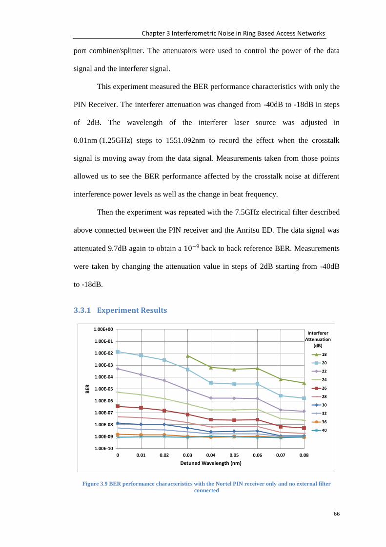
Chapter 3 Interferometric Noise in Ring Based Access Networks
66
port combiner/splitter. The attenuators were used to control the power of the data
signal and the interferer signal.
This experiment measured the BER performance characteristics with only the
PIN Receiver. The interferer attenuation was changed from -40dB to -18dB in steps
of 2dB. The wavelength of the interferer laser source was adjusted in
0.01nm (1.25GHz) steps to 1551.092nm to record the effect when the crosstalk
signal is moving away from the data signal. Measurements taken from those points
allowed us to see the BER performance affected by the crosstalk noise at different
interference power levels as well as the change in beat frequency.
Then the experiment was repeated with the 7.5GHz electrical filter described
above connected between the PIN receiver and the Anritsu ED. The data signal was
attenuated 9.7dB again to obtain a back to back reference BER. Measurements
were taken by changing the attenuation value in steps of 2dB starting from -40dB
to -18dB.
3.3.1 Experiment Results
Figure 3.9 BER performance characteristics with the Nortel PIN receiver only and no external filter
connected
1.00E-10
1.00E-09
1.00E-08
1.00E-07
1.00E-06
1.00E-05
1.00E-04
1.00E-03
1.00E-02
1.00E-01
1.00E+00
0 0.01 0.02 0.03 0.04 0.05 0.06 0.07 0.08
BER
Detuned Wavelength (nm)
18
20
22
24
26
28
30
32
36
40
Interferer Attenuation
(dB)
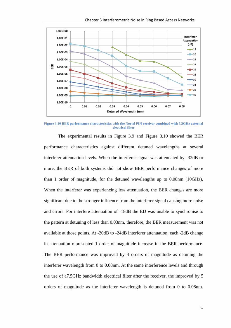
Chapter 3 Interferometric Noise in Ring Based Access Networks
67
Figure 3.10 BER performance characteristics with the Nortel PIN receiver combined with 7.5GHz external
electrical filter
The experimental results in Figure 3.9 and Figure 3.10 showed the BER
performance characteristics against different detuned wavelengths at several
interferer attenuation levels. When the interferer signal was attenuated by -32dB or
more, the BER of both systems did not show BER performance changes of more
than 1 order of magnitude, for the detuned wavelengths up to 0.08nm (10GHz).
When the interferer was experiencing less attenuation, the BER changes are more
significant due to the stronger influence from the interferer signal causing more noise
and errors. For interfere attenuation of -18dB the ED was unable to synchronise to
the pattern at detuning of less than 0.03nm, therefore, the BER measurement was not
available at those points. At -20dB to -24dB interferer attenuation, each -2dB change
in attenuation represented 1 order of magnitude increase in the BER performance.
The BER performance was improved by 4 orders of magnitude as detuning the
interferer wavelength from 0 to 0.08nm. At the same interference levels and through
the use of a7.5GHz bandwidth electrical filter after the receiver, the improved by 5
orders of magnitude as the interferer wavelength is detuned from 0 to 0.08nm.
1.00E-10
1.00E-09
1.00E-08
1.00E-07
1.00E-06
1.00E-05
1.00E-04
1.00E-03
1.00E-02
1.00E-01
1.00E+00
0 0.01 0.02 0.03 0.04 0.05 0.06 0.07 0.08
BER
Detuned Wavelength (nm)
18
20
22
24
26
28
30
32
36
40
Interferer Attenuation
(dB)

Chapter 3 Interferometric Noise in Ring Based Access Networks
68
Comparing with the case without the filter, the filtered signals have better
performances beyond 0.05nm detuning. At 0.08nm detuning, their BER performance
is on average 1 order of magnitude better than the receiver only case which
contained a filter with 10GHz bandwidth. For interferer signals attenuated by more
than 24dB, the BER performance enhancement by filtering was less effective, since
the interferometric noise was also weaker.
Figure 3.9 and Figure 3.10 can also be plotted in the classical crosstalk
representations, as in Figure 3.11 and Figure 3.12.
Figure 3.11 BER performance verses interferer attenuation levels, Nortel PIN Rx only
1.00E-10
1.00E-09
1.00E-08
1.00E-07
1.00E-06
1.00E-05
1.00E-04
1.00E-03
1.00E-02
1.00E-01
1.00E+00
-40 -35 -30 -25 -20 -15
BER
Interferer attenuation (dB)
0.00
1.25
2.50
3.75
5.00
6.25
7.50
8.75
10.00
Detuned Frequency
(GHz)
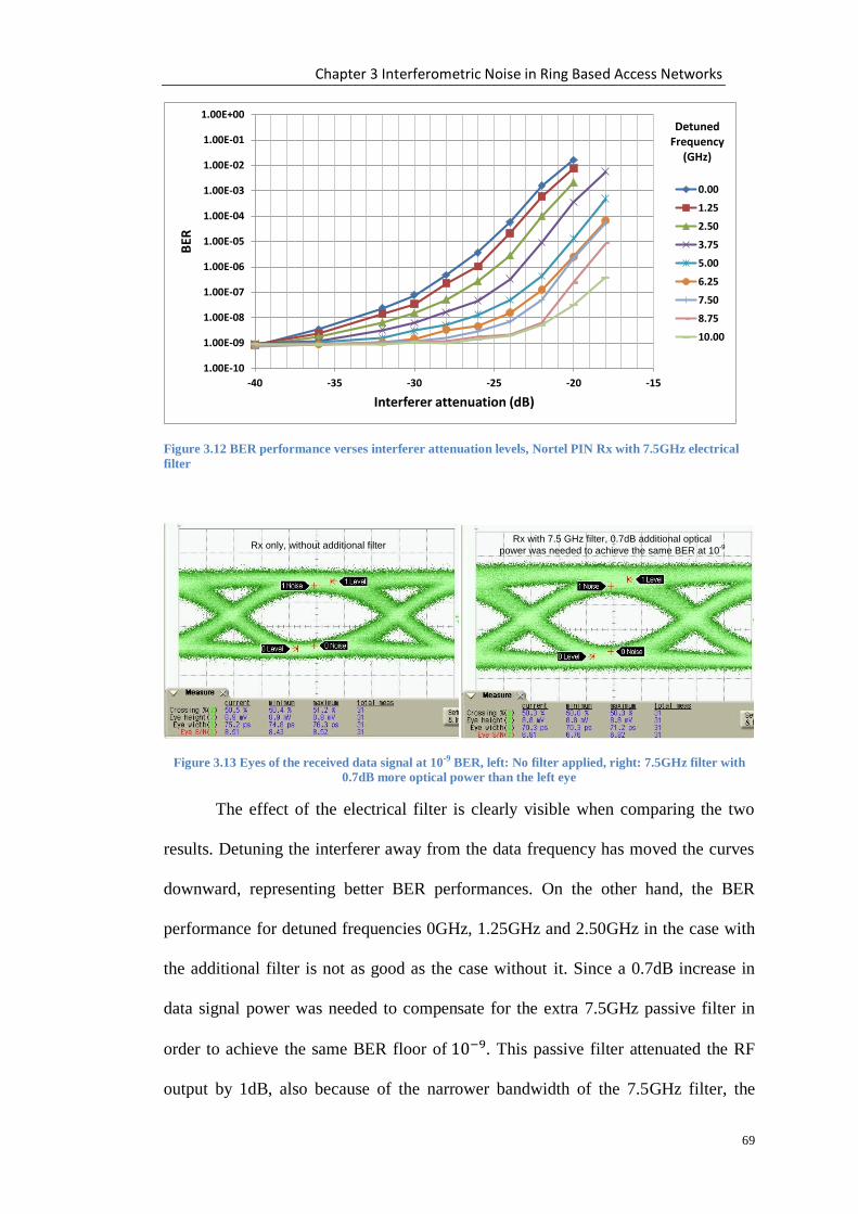
Chapter 3 Interferometric Noise in Ring Based Access Networks
69
Figure 3.12 BER performance verses interferer attenuation levels, Nortel PIN Rx with 7.5GHz electrical
filter
Figure 3.13 Eyes of the received data signal at 10-9 BER, left: No filter applied, right: 7.5GHz filter with
0.7dB more optical power than the left eye
The effect of the electrical filter is clearly visible when comparing the two
results. Detuning the interferer away from the data frequency has moved the curves
downward, representing better BER performances. On the other hand, the BER
performance for detuned frequencies 0GHz, 1.25GHz and 2.50GHz in the case with
the additional filter is not as good as the case without it. Since a 0.7dB increase in
data signal power was needed to compensate for the extra 7.5GHz passive filter in
order to achieve the same BER floor of . This passive filter attenuated the RF
output by 1dB, also because of the narrower bandwidth of the 7.5GHz filter, the
1.00E-10
1.00E-09
1.00E-08
1.00E-07
1.00E-06
1.00E-05
1.00E-04
1.00E-03
1.00E-02
1.00E-01
1.00E+00
-40 -35 -30 -25 -20 -15
BER
Interferer attenuation (dB)
0.00
1.25
2.50
3.75
5.00
6.25
7.50
8.75
10.00
Detuned Frequency
(GHz)
Rx only, without additional filterRx with 7.5 GHz filter, 0.7dB additional optical
power was needed to achieve the same BER at 10-9

Chapter 3 Interferometric Noise in Ring Based Access Networks
70
received SNR decreased by as much as 2.7dB as result of reduced eye height and eye
width along with some phase distortions. Increasing the optical power compensated
for the eye height reduction, but the eye width reduction and phase distortions after
the filter were not compensated. As can be seen from Figure 3.13, even at the same
BER, the SNR of the receiver only case is 1.7 higher than the compensated eye when
the 7.5GHz filter is applied. When the interferer is very close to the data signal
frequency, the BER performance of the case with the 7.5GHz filter will be more
sensitive to interferometric noise, as it already has a lower SNR. Therefore, when the
interferer is within 3.75GHz from the data signal frequency, the BER performance is
not as good as the case with only the receiver. The additional filter does not have a
significant effect on the interferometric noise in the region where the beat frequency
is <3.75GHz because the filter cut-off frequency is at 6GHz, so as soon as the
interferer is detuned by more than 5GHz, an improved BER performance can be seen
with the narrower bandwidth filter applied, even for an relatively lower data signal
SNR.
3.4 Simulation
3.4.1 Model of the experiment
To enable an extended investigated analysis of the impact of filtering
simulations were performed in OptSim. This platform was chosen for this simulation
requiring physical layer modelling as it considers both electrical and optical effects,
and it also allows customised filter to be imported so that comparisons between the
ideal and actual electrical filtering effects are possible. The filter response of the PIN
receiver and 7.5GHz electrical filter response were imported into OptSim, since the
electrical filters in OptSim do not have identical responses to these physical filters, to
allow validation against the experimental results.

Chapter 3 Interferometric Noise in Ring Based Access Networks
71
Figure 3.14 Simulation schematic mirroring the experimental setup
In OptSim, a sample mode simulation with an identical schematic to the
experiment setup in Figure 3.8 was constructed, as shown in Figure 3.14. The
polarisation controllers were not represented in the simulation, this is because in
OptSim the optical signal’s polarisation can be set to “single polarisation”, therefore,
the polarisation is assumed to be always aligned. This setting gives the worst case
performance when simulating interferometric noise, which served the same purpose
as the polarisation controllers used in the experiment. The signal bit streams are
generated by a PRBS logical source and then it is converter to an electrical signal by
a laser driver module. The external laser modulator then modulates this electrical
signal on to a CW signal generated by a laser with linewidth at 1 MHz, which is the
same as the datasheet specified DFB laser linewidth used in the experiment. The
modulator has a realistic ER of 10.3dB to match those measured during the
experiment. In this simulation, a Pseudo Random Bit Sequence (PRBS) electrical
signal is generated for both the source and interferer, except the interferer signal was
passed through a fibre module in OptSim that is 4km longer than the source signal to
decorrelate the bit streams. These two de-correlated optical signals were then passed
through a 50:50 dual input and dual output optical coupler and fall on to the PIN
receiver.

Chapter 3 Interferometric Noise in Ring Based Access Networks
72
The wavelength of the interferer laser could be adjusted at each simulation
run to simulate the effect of the wavelength of the crosstalk signal moving away
from the data signal. The interferer laser source was turned off initially to allow a
reference BER of to be obtained from the data signal. The power of the
interferer signal was controlled by an attenuator while the data signal attenuation was
held at the value used to obtain the reference BER.
The data signal’s laser wavelength was set to 1551.012 nm. This value is the
same as the fixed wavelength laser source used in the later experiment. The crosstalk
laser wavelength was also set to 1551.012 nm to simulate the heterodyne incoherent
beat noise crosstalk condition, this wavelength was then changed each run at 0.01
nm step with a total of 8 steps to 1551.092 nm so that wavelength detuning of up to
0.08nm can be simulated. The interferer attenuation was changed at the same steps
as the experiment.
Similar to the experiments, the simulation was carried out for two conditions.
The first condition is when only the internal 11GHz bandwidth post detection filter is
present between PIN receiver and the ED; the second condition is when the Receiver
and its internal 11GHz bandwidth filter is combined with a 7.5GHz low-pass filter.
The filter responses are made by importing the frequency responses of the PIN
receiver and the combine frequency response of the PIN receiver with the
Picosecond 7.5GHz filter into OptSim’s customised filter. The frequency responses
were measured on a Lightwave Component Analyser (LCA) and then imported into
OptSim.

Chapter 3 Interferometric Noise in Ring Based Access Networks
73
3.4.2 Simulation Results
Figure 3.15 BER performance simulated characteristics with PIN receiver only and no external filter
applied
Figure 3.16 BER performance simulated characteristics with PIN receiver combined with customised filter
using the measured filter response from the 7.5GHz filter used in the experiment
These simulation results show similar trends to the experimental data. A
detailed comparison of the simulation results with the experiment results will be
presented in the next section.
1.00E-10
1.00E-09
1.00E-08
1.00E-07
1.00E-06
1.00E-05
1.00E-04
1.00E-03
1.00E-02
1.00E-01
1.00E+00
0.00 0.01 0.02 0.03 0.04 0.05 0.06 0.07 0.08
BER
Detuned Wavelength (nm)
18dB
20dB
22dB
24dB
26dB
28dB
30dB
32dB
34dB
36dB
Attenuation (dB)
1.00E-09
1.00E-08
1.00E-07
1.00E-06
1.00E-05
1.00E-04
1.00E-03
1.00E-02
1.00E-01
1.00E+00
0.00 0.01 0.02 0.03 0.04 0.05 0.06 0.07 0.08
BER
Detuned Wavelength (nm)
18dB
20dB
22dB
24dB
26dB
28dB
30dB
32dB
34dB
36dB
Attenuation (dB)

Chapter 3 Interferometric Noise in Ring Based Access Networks
74
The simulation results can also be represented in the classical crosstalk plot,
as in Figure 3.17 and Figure 3.19.
Figure 3.17 Simulated BER performance verses interferer attenuation levels for Rx only case
Figure 3.18 Simulated BER performance verses interferer attenuation levels for the PIN Rx + 7.5GHz
filter case
1.00E-10
1.00E-09
1.00E-08
1.00E-07
1.00E-06
1.00E-05
1.00E-04
1.00E-03
1.00E-02
1.00E-01
1.00E+00
-40 -35 -30 -25 -20 -15
BER
Interferer attenuation (dB)
0.00
1.25
2.50
3.75
5.00
6.25
7.50
8.75
10.00
Detuned Frequency
(GHz)
1.00E-09
1.00E-08
1.00E-07
1.00E-06
1.00E-05
1.00E-04
1.00E-03
1.00E-02
1.00E-01
1.00E+00
-40 -35 -30 -25 -20 -15
BER
Interferer attenuation (dB)
0.00
1.25
2.50
3.75
5.00
6.25
7.50
8.75
10.00
Detuned Frequency
(GHz)

Chapter 3 Interferometric Noise in Ring Based Access Networks
75
3.5 Analysis of Experiment and Simulation Results
The simulation results will need to be validated by the experiment so that the
simulated system can be used in the varying filter bandwidth analysis. Since there
are many sets of results to compare, in order to make the presentation clear, only the
results at the -20dB interferer attenuation level were compared. Among all the fully
measured experiment and simulation results, this set of result was chosen because it
represents the strongest effect of the interferer which lead to the largest change in
BER, as the wavelength of the interferer was being detuned away from the source
wavelength.
Figure 3.19 Comparing simulation and experiment results at -20dB interferer attenuations with PIN Rx
only
Both the simulated BER and the measured BER from the experiment
at -20dB interferer attenuation level is shown in Figure 3.19, they follow the same
trend of increased BER performance as the interferer moves away from the source,
and the resulting points are very similar for detuned wavelengths 0.03nm and
0.08nm, the differences increased to 1 order of magnitude when no detuning was
performed, i.e. when the frequency separation between the interferer and the source
is <3.75GHz. This difference could arise from the BER estimator in the simulation
which calculates the BER from the Q-factor of the received simulated eye. The
1.00E-07
1.00E-06
1.00E-05
1.00E-04
1.00E-03
1.00E-02
1.00E-01
1.00E+00
0 0.01 0.02 0.03 0.04 0.05 0.06 0.07 0.08
BER
Detuned wavelength (nm)
Experiment (-20dB)
Simulation with measuredfilter response (-20dB)
Simulation with simulatedBessel filter (-20dB)

Chapter 3 Interferometric Noise in Ring Based Access Networks
76
simulated system estimates the BER instead of counting the actual error in contrast
to the ED in the experimental setup, to reduce memory requirement and simulation
time.
Figure 3.20 Comparing simulation and experiment results at -20dB interferer attenuations with PIN Rx +
7.5 GHz filter
Similar observations were found in Figure 3.20 where an additional 7.5GHz
filter is used in combination with the receiver, with the largest difference between
the experimental results and the simulated results being one order of magnitude. In
the two simulation results, the BER of the imported filter response and the simulated
response of the 4th
Order Bessel filter differed by less than 1 order of magnitude.
Looking at the classical crosstalk representations, comparisons between the
simulation and experiment results also show the accuracy of the simulation in
estimating the BER performance from the received signal eye, the comparisons are
shown in Figure 3.21 and Figure 3.22.
1.00E-10
1.00E-09
1.00E-08
1.00E-07
1.00E-06
1.00E-05
1.00E-04
1.00E-03
1.00E-02
1.00E-01
1.00E+00
0 0.01 0.02 0.03 0.04 0.05 0.06 0.07 0.08 0.09
BER
Detuned Wavelength (nm)
Experiment, 7.5GHz filter (-20dB)
Simulation, 7.5GHz simulated Bessel filter (-20dB)
Simulation, 7.5GHz measured filter(-20dB)

Chapter 3 Interferometric Noise in Ring Based Access Networks
77
Figure 3.21 Comparing simulation and experiment results at 0,5,10 GHz frequency separation, Rx only
case, “Sim” indicates Simulation result and “Exp” indicates Experiment result
Figure 3.22 Comparing simulation and experiment results at 0,5,10 GHz frequency separation, Rx +
7.5GHz filter case, “Sim” indicates Simulation result and “Exp” indicates Experiment result
In both cases, detuned frequencies of 0, 5 and 10 GHz were selected for
comparison to keep the result clear. For the receiver only case, the two sets of results
matches closely at 0GHz and 10GHz frequency separation, where the BER
difference is less than half an order of magnitude, at 5GHz frequency separation, the
results has a larger BER difference that is 1 order of magnitude, at -22dB to -26dB
interferer attenuation levels. For the case of receiver and filter combined, the two
sets of result did not match as well, large differences between the simulated and
1.00E-10
1.00E-09
1.00E-08
1.00E-07
1.00E-06
1.00E-05
1.00E-04
1.00E-03
1.00E-02
1.00E-01
1.00E+00
-40 -35 -30 -25 -20 -15
BER
Interferer attenuation (dB)
0.0 Sim
0.0 Exp
5.0 Sim
5.0 Exp
10.0 Sim
10.0 Exp
Detuned Frequency
(GHz)
1.00E-10
1.00E-09
1.00E-08
1.00E-07
1.00E-06
1.00E-05
1.00E-04
1.00E-03
1.00E-02
1.00E-01
1.00E+00
-40 -35 -30 -25 -20 -15
BER
Interferer attenuation (dB)
0.0 Sim
0.0 Exp
5.0 Sim
5.0 Exp
10.0 Sim
10.0 Exp
Detuned Frequency
(GHz)

Chapter 3 Interferometric Noise in Ring Based Access Networks
78
experiment results also occurs at 5GHz frequency separation (or 0.04nm detuned
interferer wavelength), with the largest difference being 1.5 order of magnitude apart.
This difference is again due to the fact that the simulation estimated the BER using
the Q-factor, the optimum decision threshold of the BER estimator was also
determined by assuming the arc-sine (another description is “two pronged”)
distributed interferometric noise as a Gaussian distributed noise. The biggest
difference occurs at half way through the detuning which is 5GHz, could be due to
the fact that this area is there a Gaussian approximation would give a large error in
decision threshold and thus Q-factor and BER estimation error. It is known that
using a narrower filter bandwidth can revert the arc-sine distributed noise to a
Gaussian-like shape [67], the following analysis presents how the noise term changes
as a result of detuning the interferer and it was carried out using the 4th
order Bessel-
Thompson filter.
3.5.1 The Effects of Receiver Electrical Filter Bandwidths
This section aims to investigate the effect of electrical filter on the
interferometric noise, at the presence of a frequency detuned interferer. In the
experiment, a fixed bandwidth 4th order Bessel-Thompson filter was. In this section,
we discuss how alternative filter bandwidth can affect the BER performance. The
general Bessel-Thompson filter has the following transfer function:
( )
∑
(3.5)
Where B is the filter coefficient used for designing analogue filters [68] and n
is the order of the filter, which at 4th order, becomes:
( )
(3.6)
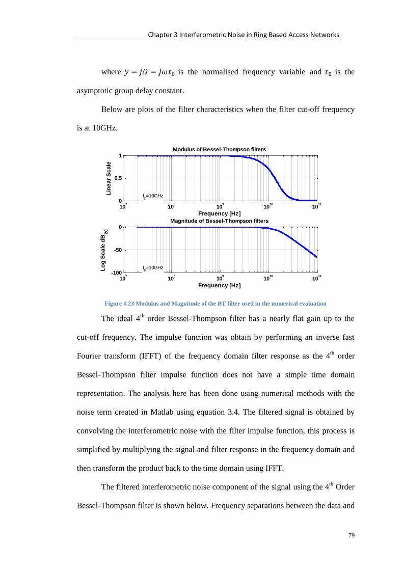
Chapter 3 Interferometric Noise in Ring Based Access Networks
79
where is the normalised frequency variable and is the
asymptotic group delay constant.
Below are plots of the filter characteristics when the filter cut-off frequency
is at 10GHz.
Figure 3.23 Modulus and Magnitude of the BT filter used in the numerical evaluation
The ideal 4th
order Bessel-Thompson filter has a nearly flat gain up to the
cut-off frequency. The impulse function was obtain by performing an inverse fast
Fourier transform (IFFT) of the frequency domain filter response as the 4th
order
Bessel-Thompson filter impulse function does not have a simple time domain
representation. The analysis here has been done using numerical methods with the
noise term created in Matlab using equation 3.4. The filtered signal is obtained by
convolving the interferometric noise with the filter impulse function, this process is
simplified by multiplying the signal and filter response in the frequency domain and
then transform the product back to the time domain using IFFT.
The filtered interferometric noise component of the signal using the 4th
Order
Bessel-Thompson filter is shown below. Frequency separations between the data and
107
108
109
1010
1011
0
0.5
1Modulus of Bessel-Thompson filters
Frequency [Hz]
Lin
ea
r S
ca
le
fc=10GHz
107
108
109
1010
1011
-100
-50
0Magnitude of Bessel-Thompson filters
Frequency [Hz]
Lo
g S
ca
le d
B2
0
fc=10GHz

Chapter 3 Interferometric Noise in Ring Based Access Networks
80
the interferer of 10, 7.5 and 5 GHz are shown in Figure 3.24, Figure 3.25 and Figure
3.26 respectively.
Figure 3.24 Normalised occurrence of the filtered noise term, when the signal-crosstalk separation is at
10GHz, Interferer power is 15dB below the data signal
Figure 3.25 Normalised occurrence of the filtered noise term, when the signal-crosstalk separation is at
7.5GHz, Interferer power is 15dB below the data signal
0.7 0.8 0.9 1 1.1 1.2 1.3 1.40
5
10
15
20
25
30
35
40
45
50
Filtered Interferometric noise amplitude, Frequency separation = 10 GHz
No
rma
lis
ed
Oc
cu
rre
nc
e
Un-filtered crosstalk
Filter BW = 2.5 GHz
Filter BW = 5 GHz
Filter BW = 7.5 GHz
Filter BW = 10 GHz
Filter BW = 12.5 GHz
0.7 0.8 0.9 1 1.1 1.2 1.3 1.40
5
10
15
20
25
30
35
40
45
50
Filtered Interferometric noise amplitude, Frequency separation = 7.5 GHz
No
rma
lis
ed
Oc
cu
rre
nc
e
Un-filtered crosstalk
Filter BW = 2.5 GHz
Filter BW = 5 GHz
Filter BW = 7.5 GHz
Filter BW = 10 GHz
Filter BW = 12.5 GHz

Chapter 3 Interferometric Noise in Ring Based Access Networks
81
Figure 3.26 Normalised occurrence of the filtered noise term, when the signal-crosstalk separation is at
5GHz, Interferer power is 15dB below the data signal
From Figure 3.24 through to Figure 3.26 it can be seen clearly that as the
signal and interferer moves further apart, the filtering becomes more effective at
reducing the interferometric noise’s width. If the width of the interferometric noise is
large it may cross over the detection threshold and cause error during detection, thus
decreasing the BER performance.
Figure 3.27 Summarising the results in Figure 3.24, Figure 3.25 and Figure 3.26
The results are summarised in Figure 3.27, it was seen that with a large
frequency separation of 10GHz, the narrowing of the filter bandwidth from 12.5GHz
0.7 0.8 0.9 1 1.1 1.2 1.3 1.40
5
10
15
20
25
30
35
40
45
50
Filtered Interferometric noise amplitude, Frequency separation = 5 GHz
No
rma
lis
ed
Oc
cu
rre
nc
e
Un-filtered crosstalk
Filter BW = 2.5 GHz
Filter BW = 5 GHz
Filter BW = 7.5 GHz
Filter BW = 10 GHz
Filter BW = 12.5 GHz
0
0.1
0.2
0.3
0.4
0.5
0.6
0.7
0.8
0 2 4 6 8 10 12 14
No
rmal
ise
d W
idth
of
IN A
mp
litu
de
Filter Bandwidth (GHz)
10GHz
7.5GHz
5GHz
Detuned Frequency
(GHz)

Chapter 3 Interferometric Noise in Ring Based Access Networks
82
to 7.5GHz filter bandwidth is able to reduce the amplitude width of the noise
component by about 0.2 unit of normalised noise amplitude. While narrowing to a
5GHz filter bandwidth the width can be reduced by 0.4 unit, this represent the high
occurrence peak of the interferometric noise having moved away from the detection
threshold by 0.1 and 0.2 units respectively. As the frequency separation between the
data and interferer reduced to 7.5GHz then 5GHz, the bandwidth of the filter
becomes less effective. At 5GHz filter bandwidths, the noise width reduction is only
0.3 and 0.2 units for 7.5 and 5 GHz frequency separations, respectively. This
explains why in both the experiment and the simulation results the BER performance
could be up to 5 orders of magnitude better as the interferer is detuned by 0.08nm
(10GHz) away from the data signal frequency, especially for high interferer powers
levels. The filter bandwidth of 2.5GHz are also included for reference, but it will be
unlikely that using this filtering bandwidth will improve the BER performance, on
the contrary, if the filter bandwidth is too low e.g. when less than 5GHz, the receiver
and filter may removing parts of desired data signal along with the interferometric
noise, causing inter symbol interference (ISI), because the high frequency
components were filtered and this cause the received eye width to reduce as a result.
Figure 3.28 Simulated BER performance for a range of ideal Bessel filter bandwidths, data and interferer
at 10GHz frequency separation
1.00E-10
1.00E-09
1.00E-08
1.00E-07
1.00E-06
1.00E-05
1.00E-04
5.0 6.0 7.0 8.0 9.0 10.0 11.0
BER
Simulation generated filter bandwidth (GHz)
20dB
22dB
24dB
InterfererAttenuation
(dB)

Chapter 3 Interferometric Noise in Ring Based Access Networks
83
The BER performance of the simulated system with filter bandwidth ranging
from 5 to 11 GHz is shown in Figure 3.28, here the data and interferer frequency
separation is 0.08nm (10GHz). For a filter bandwidth of 7GHz, the received signal
have the best BER performance, at higher bandwidth the received signal
performance is interferometric noise limited, and at lower than 7GHz bandwidth, the
BER performance start to decrease due to ISI. When the bandwidth of the filter is
higher than the receiver’s internal filter bandwidth, the system performance is
determined by the smallest filter bandwidth, in this case the receiver’s bandwidth.
3.6 Conclusions
In this chapter, we have investigated and the relationship between the BER
performance and the electrical filter characteristics for various levels of interferer
power, in the condition when interferometric noise is present. The less strictly
defined wavelength unique to access networks was taken into account for the first
time. The experiment results demonstrated that, for > 0.04 nm (5 GHz) interferer
detuning, by adding a 7.5GHz bandwidth electronic filter after the 10Gb/s PIN
receiver, the received BER performance is better than using a receiver alone (11GHz
internal filter bandwidth). A simulation of the experimental system was also
constructed in order to analyse a full range of filter bandwidths. The simulation
system was validated by comparing to the experiment results, same trends were
observed and the largest difference between the simulated and measured BER
performance is less than 1.5 orders of magnitude apart.
An analytical model was also developed to evaluate the impact of receiver
filter bandwidth on IN, the frequency separation between the interferer and data
caused by not strictly defined wavelength was taken into account. In conclusion, the
BER performance characteristics will change with the choice of electrical filtering in

Chapter 3 Interferometric Noise in Ring Based Access Networks
84
the receiver. It was found that using a narrower filter at 70% of the receiver
bandwidth can reduce the interferometric noise amplitude while not causing
significant ISI. The effectiveness of the filtering increases with the frequency
separation of the data and the interferer, resulting in performance gain of the
received data signal.
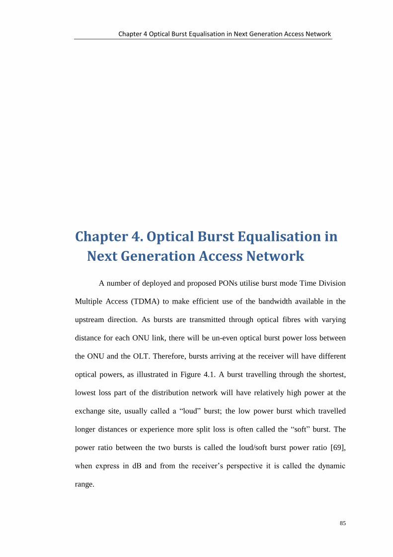
Chapter 4 Optical Burst Equalisation in Next Generation Access Network
85
Chapter 4. Optical Burst Equalisation in
Next Generation Access Network
A number of deployed and proposed PONs utilise burst mode Time Division
Multiple Access (TDMA) to make efficient use of the bandwidth available in the
upstream direction. As bursts are transmitted through optical fibres with varying
distance for each ONU link, there will be un-even optical burst power loss between
the ONU and the OLT. Therefore, bursts arriving at the receiver will have different
optical powers, as illustrated in Figure 4.1. A burst travelling through the shortest,
lowest loss part of the distribution network will have relatively high power at the
exchange site, usually called a “loud” burst; the low power burst which travelled
longer distances or experience more split loss is often called the “soft” burst. The
power ratio between the two bursts is called the loud/soft burst power ratio [69],
when express in dB and from the receiver’s perspective it is called the dynamic
range.

Chapter 4 Optical Burst Equalisation in Next Generation Access Network
86
Figure 4.1 PON upstream with ONU located at uneven distance resulting in burst power difference
In the current GPON and EPON standards the transmission distance may be
up to 20km, however, distances of 60km or even 100km have been proposed for the
next generation access [39]. Therefore, the dynamic range or differential path loss
due to burst-burst power variations may exceed the network specified, for example
15dB requirement in the GPON standard. Standard continuous mode receivers are
not designed to adapt to these power variations or achieve phase alignment on a
burst-by-burst basis in a nanosecond time scale. This will be especially critical in
Next Generation PONs (NG-PONs) where the threshold adjustment time will be
even shorter due to the higher data rate. Burst mode receivers (BMR) are available
for current 2.5Gb/s GPON, and although they are beginning to emerge for NG-PON,
the 10Gb/s BMR’s complexity and high cost may be reduced if a burst equalisation
scheme was employed at the local exchange or just before the OLT.
In a backhaul amplified PON network, the optical amplification can usually
be achieved by using EDFAs or SOAs. Since the power level of the OLT transmitter
is constant and the EDFA have a high gain and low noise figure, this makes EDFA
ideal for broadcast type downstream transmission. In the upstream direction, the data
is transmitted from several ONUs in a series of bursts to the OLT, in order to avoid
noise funnelling, the ONUs need to be gated, which mean it is only switched on for
125μs at each burst of data. Both the “loud” and “soft” burst will appear in the
upstream, this on-going optical power change requires the intermediate site upstream
ONU 1
ONU 2
ReceiverONU 3
Splitter
Power
Time15km
1km
8km
15km 1km 8km
20 to 100km

Chapter 4 Optical Burst Equalisation in Next Generation Access Network
87
optical amplifier to have a fast gain recovery time in order to maintain a near
constant intra-burst power levels. If the gain recovery time is too long and the
intra-burst power difference is too large, then the preamble used by the receiver to
initially set the decision threshold will not be the optimum threshold for the data
payload. As mention in section 2.2.2, EDFAs have a relatively long gain recovery
time at 110 to 340μs which is too slow compared to the 125μs burst duration in
current PON requirements. In this aspect, the SOAs have many advantages for the
upstream burst-mode operation, including high gain and fast gain recovery time at
typically 280ps [70]. Recent research and proposed future access network
technology [4, 14] also indicate that SOAs or EDFAs will be placed in PONs as
reach extenders. As these active optical amplifiers are already part of the network,
they could be used for all-optical burst equalisation with minimal modification to the
network and could potentially allow standard receiver components to be used, further
reducing the cost of the access network.
Figure 4.2 PON upstream with burst equalisation using an optical limiting amplifier
The gain saturation effect of the Semiconductor Optical Amplifier (SOA)
enables it to act as an optical limiting amplifier, reducing the difference in burst
amplitudes and allowing the bursts to have similar detection thresholds at the
receiver as shown in Figure 4.2. The advantage over electronic burst mode receiver
is that the need for rapidly variable threshold detection and adjustment is removed,
possibly allowing much cheaper burst mode receiver or even standard receivers to be
ONU 1
ONU 2
Before Equalisation
Standard
Rx
After Equalisation
Limiting Optical Amplifier20km
20 to 100km
1 km

Chapter 4 Optical Burst Equalisation in Next Generation Access Network
88
used. This chapter reports on the investigation of this concept of using the SOA as a
limiting amplifier to achieve power equalisation of optical bursts by both simulation
and experiment. We also suggest that appropriate optical filtering may to be
implemented to minimise the effect of spectral broadening of the equalised signal as
a result of the SOA saturation.
In this chapter, section 4.1 explains the SOA characteristics and the reason
that saturation of the SOA can cause non-linear effects in the amplified signal.
Section 4.2 describes the modelling of pulse travelling through the saturated SOA, it
also explains the chirp and spectral characteristics. Section 4.3 applies the model to
bursts of binary data, the burst are at different power. An extension of the model was
also applied and they are compared in terms of their accuracy to simulate the output
signal in the time domain and the saturation characteristics of the SOA. The
shortcomings of the models used are explained and future adjustment to the model is
also suggested. Section 4.4 explains the saturation induced spectral broadening and a
solution to reduce the non-linear effect by optical filtering. Section 4.5 describes and
analyse the results of the experiment that was set up to test the burst levelling using
saturated SOAs and the use of optical filtering to reduce the non-linear effects
caused by saturation.
4.1 SOA Characteristics
4.1.1 Non-linear Gain Saturation of the SOA
The amplification operation of SOA is based on the population inversion of
electrons and the stimulated emission process in the SOA active region. This
stimulated emission is optically confined to the active region due to the refractive
index difference which exists between the active region and the cladding p-type and
n-type regions. The fraction of the energy confined within the active region is known

Chapter 4 Optical Burst Equalisation in Next Generation Access Network
89
as the optical confinement factor Г [71]. As described in section 2.2.3, the population
inversion is maintained by electrically pumping the SOA. When the input signal
power is high, the rate of pumping is insufficient to keep a large number of electrons
in the excited state. The SOA is considered in saturation because the rate pumping is
limiting the rate of photon emissions and therefore, limiting the gain. The following
experimental characterisations measured the non-linear gain saturation of the SOAs
used in this work.
Two optical amplifier models were available, one designed as a pre-amplifier
and one as a booster amplifier. The saturation characteristics of the pre-amplifier
SOAs (Kamelian OPA-20NC-FA) used in the experiment were measured with an
EDFA amplified CW laser input to drive the SOA into saturation. The input verses
output power and the gain saturation characteristics are presented in Figure 4.3. The
booster amplifier (Kamelian OPB-15NC-FA) characteristic is shown in Figure 4.4.
Figure 4.3 Pre-amp SOA input/output power and static gain saturation characteristic
-30 -25 -20 -15 -10 -5 0 5 10 15-10
0
10
20
Ou
tpu
t P
ow
er
(dB
m)
-30 -25 -20 -15 -10 -5 0 5 10 150
10
20
30
Input Power (dBm)
Ga
in (
dB
)
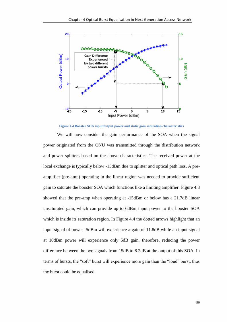
Chapter 4 Optical Burst Equalisation in Next Generation Access Network
90
Figure 4.4 Booster SOA input/output power and static gain saturation characteristics
We will now consider the gain performance of the SOA when the signal
power originated from the ONU was transmitted through the distribution network
and power splitters based on the above characteristics. The received power at the
local exchange is typically below -15dBm due to splitter and optical path loss. A pre-
amplifier (pre-amp) operating in the linear region was needed to provide sufficient
gain to saturate the booster SOA which functions like a limiting amplifier. Figure 4.3
showed that the pre-amp when operating at -15dBm or below has a 21.7dB linear
unsaturated gain, which can provide up to 6dBm input power to the booster SOA
which is inside its saturation region. In Figure 4.4 the dotted arrows highlight that an
input signal of power -5dBm will experience a gain of 11.8dB while an input signal
at 10dBm power will experience only 5dB gain, therefore, reducing the power
difference between the two signals from 15dB to 8.2dB at the output of this SOA. In
terms of bursts, the “soft” burst will experience more gain than the “loud” burst, thus
the burst could be equalised.
-20 -15 -10 -5 0 5 10 15-10
0
10
20
Ou
tpu
t P
ow
er
(dB
m)
Input Power (dBm)-20 -15 -10 -5 0 5 10 15
0
5
10
15
Ga
in (
dB
)
Gain Difference
Experienced
by two different
power bursts

Chapter 4 Optical Burst Equalisation in Next Generation Access Network
91
Figure 4.5 Booster SOA output power saturation characteristics at different SOA bias current
The pre-amp has a fibre to fibre maximum or unsaturated gain of 21.7dB and
the booster has a maximum gain of about 12dB, while they both have a saturation
output power Po,sat at around 12.5dBm, which is defined as the amplifier output
signal power when the amplifier gain has fallen by 3dB from its small-signal gain
maximum[72]. The output power in deep saturation can reach as high as 15.5dBm in
this static characterisation with a CW input. From Figure 4.5 it can be seen that the
maximum saturation power depends non-linearly on the bias current, this
characteristic can be explained by the number of electrons pumped into the device
and the electron depletion as a result of gain saturation. Higher input bias current
results in higher output power for the same input power, which effectively increases
the saturated output power and the gain at high saturation. This is because an
increase in bias current directly increased the number of electrons being pumped into
the SOA and the electron depletion rate will therefore, be balanced out by the
pumping which makes it harder for the SOA to saturate. It is also observed that the
unsaturated gain does not change linearly with bias current, when the bias current is
above a certain threshold, in this case 70mA, the increase in unsaturated gain is very
-10
-5
0
5
10
15
20
-20 -15 -10 -5 0 5 10 15
Ou
tpu
t P
ow
er P
ou
t (d
Bm
)
Input Power Pin (dBm)
Pout(dBm) @ 200 mA Input Current
Pout(dBm) @ 100 mA Input Current
Pout(dBm) @ 50 mA Input Current

Chapter 4 Optical Burst Equalisation in Next Generation Access Network
92
small compared to the increase in bias current. This is because in the unsaturated
region, above the threshold bias current the electron density becomes sufficient for
stimulated recombination and the unsaturated gain has reached its maximum. In the
following experiments a 200mA bias current was used for both SOAs, because it is
the typical operating bias current for this SOA which provides high gain and fast
gain recovery. The gain recovery time decreases with increasing bias current and the
length of the SOA active region, it is usually 200ps for commercially available
SOAs [36].
Modulated optical signals contain the energies carried by the binary “0s” and
binary “1s”. For a semiconductor laser with an external modulator the energy
emitted in the binary 0 bit period is non-zero, with the value depending on the design
and drive of the modulator. The Extinction Ratio (ER) is defined as the ratio between
the power associated with the “1s”, P1, and the power associated with the “0s”, P0.
( ) (
)
The SOAs amplifies both the energies of the “1s” and the energies of the
“0”s. The addition of amplified spontaneous emission (ASE) noise as a result of
using the SOA effectively reduces the ER, therefore, keeping the ER high while
amplifying/levelling the signals is desirable but will be difficult, because there are
also saturation induced distortions that occur at gain saturation due to the carrier
density modulation, which also reduces the ER and hence impact the performance of
the equalised signal.
4.1.2 Saturation Induced Phase Modulation in the SOA
The normal use of SOA is for amplifying modulated continuous optical
signals, if the signal power is high then gain saturation will occur and this will not be

Chapter 4 Optical Burst Equalisation in Next Generation Access Network
93
a major problem if the SOA gain dynamic is a slow process. The gain dynamics of
an SOA is determined by the carrier recombination lifetime, which is typically
hundreds of picoseconds. With a 10Gb/s modulated signal at the input to the SOA,
the gain dynamics of the SOA used in NG-PON will be very fast as the pulse width
is only 100ps which is in the same order as the carrier recombination lifetime.
Furthermore, for the purpose of signal power levelling or equalisation, the booster
SOA will be operating in saturation mode, hence a SOA model that considers the
fast gain dynamics is needed for the performance analysis of the burst equalisation
system.
Considering a SOA operating in deep saturation, as the signal power
increases the electrons in the active region become depleted resulting in a decrease in
amplifier gain. A fast changing modulated signal will cause fast depletion and
injection of electrons into the SOA active region, which changes the refractive index
as a result of the Kramers–Kronig Relations [72]. Therefore, operating the SOA
under deep saturation will equalise the signal power but it can also cause unwanted
distortions in the equalised signal due to the carrier density modulation in the SOA
active region. The distortions in the equalised signal may damage performance, they
will need to be taken into account when simulating and modelling the optical burst
equalisation system. The refractive index change in an SOA active region may be
understood through the complex refractive index ( ) ( ) ( ), where the
real component is the real part of the refractive index representing phase
modulation, and the imaginary component indicates the gain modulation within
the active region [44]. The parameter relating these two components is the linewidth
enhancement factor (also known as the chirp parameter) α, [44].

Chapter 4 Optical Burst Equalisation in Next Generation Access Network
94
Considering an electromagnetic wave propagating in the z-direction through
the SOA, it can be described using the equation:
( ) [ ( )] (4.1)
where
is the field constant,
β = 2π/λm = (ω/c)n is the propagation constant relating to the refractive index,
n is the refractive index,
λm = λ/n is the local wavelength in the propagation medium,
λ is the free-space propagation wavelength, and ω = 2πf is the angular
frequency.
When an input signal travels through an SOA it will cause carrier density
modulation, which changes the propagation constant β via refractive index
modulation, therefore, the phase of the propagating signal is modulated by the β
parameter and by the change in refractive index.
When the gain of the active region is saturated by an incoming pulse, it does
not recover instantly. The leading edge of the input pulse will experience the full
gain while the trailing edge experiences less gain as the gain saturates during the
pulse. The phase change in this process is characterised by Agrawal’s equation [42] :
( ) (4.2)
where
ϕ is the phase,
α is the linewidth enhancement factor or chirp parameter and,

Chapter 4 Optical Burst Equalisation in Next Generation Access Network
95
g is the time dependent gain of the active region.
Since the incoming pulse modulates its own phase at gain saturation, this
phenomenon is also called Self Phase Modulation (SPM).
4.2 Simulating Self Phase Modulation with a Single Pulse
A dynamic model that considers the SPM effects is the SOA model required
in this work. The first part of this study is based on Agrawal’s model [42]. The
model is a dynamic description of the signal in the SOA, taking into account the
temporal characteristics of the carrier lifetime. It was first written in Matlab code
based on the following theory and equations and will later be used in OptSim as a
CCM (Custom Component for Matlab).
[ ( ) ] (4.3)
where
is the natural logged gain, i.e. [ ( )], of the SOA active region,
is the small signal gain,
is the carrier lifetime,
is the input pulse instantaneous power,
is the saturation energy and,
note here that ( ) is the unsaturated amplifier gain [42].
The output pulse shape can then be obtained from this equation:
( ) ( ) [ ( )] (4.4)
where is the instantaneous output pulse power. The term ( ) is the gain
of this theoretical SOA and is solved from Equation 4.1 using the Runge-Kutta 4th
Order numerical integration methods.

Chapter 4 Optical Burst Equalisation in Next Generation Access Network
96
The frequency chirp is also given in [42], based on the phase change
described earlier.
[ ( ) ] (4.5)
A Matlab simulation of a travelling pulse was created by using Equations 4.1
to 4.3, the results generated and shown in Figure 4.6 through to Figure 4.8 was
validated by comparing with the results given by the paper [42]. This validation
process was important because it can reveal errors in the programming and it can
confirm that the time domain and frequency domain signal behaviours are identical
to the known results before moving on to using the model for further simulations.
Figure 4.6 Time domain signal frequency shifted
-3 -2 -1 0 1 2 30
0.2
0.4
0.6
0.8
1
Normalised Time / o
No
rma
lis
ed
Po
we
r
Gain=0dB
Gain=30dB

Chapter 4 Optical Burst Equalisation in Next Generation Access Network
97
Figure 4.7 Chirp of the Gaussian pulse
Figure 4.8 Power Spectra of the shifted signal
The model was successfully validated because all three simulation results are
identical to the ones presented in Agrawal’s paper [42] for a Gaussian pulse input,
with a linewidth enhancement factor of 5. As well as validating the model, these
results also provide easy to understand details of the SPM and chirping of the input
pulse. A shift of the pulse towards the lower frequency side was observed as the
amplifier gain increases to 30dB. The leading edge of the pulse has a higher gradient
-3 -2 -1 0 1 2 3-1
-0.9
-0.8
-0.7
-0.6
-0.5
-0.4
-0.3
-0.2
-0.1
0
Normalised Time / o
Ch
irp
ou
t o
Gain=30dB
-3 -2.5 -2 -1.5 -1 -0.5 0 0.5 1 1.5 20
0.1
0.2
0.3
0.4
0.5
0.6
0.7
0.8
0.9
1
Normalised Frequency ( - o) /
o
No
rma
lis
ed
Po
we
r
Gain=0dB
Gain=30dB

Chapter 4 Optical Burst Equalisation in Next Generation Access Network
98
than the trailing edge of the pulse, because the leading edge experienced more gain
thus higher magnitude of phase shift than the trailing edge. The chirp shape in Figure
4.7 corresponds to the frequency shift in Figure 4.6, the power spectra in Figure 4.8
also showed a shift towards the low frequency side which resulted in spectral
broadening of the pulse. It is expected that with a large number of pulses, the chirp
effect on a signal pulse is re-produced on every bit of the actual signal that travel
through the amplifier under saturation, which cause significant overall spectral
broadening in the received signal spectrum.
4.3 Simulating the Equalisation of Bursts
The RSoft OptSim package was used to perform system simulation of optical
networks. OptSim is designed for simulating and analysing signal propagation and
performance of optical systems, it contains a large amount of built-in components
such as lasers, modulators and measurement probes. This allows fast prototyping of
an optical system, it also considers logical and electrical signals, so that the input
signal can be adjusted to suit the need of the system. The physical layer burst
structure was deduced from the GPON standard’s upstream frame structure [29] and
applied using 10Gb/s data rate, as the burst structure information in the NG-PON
standard was not available at the time of this work. It is also expected that NG-PON
will have a similar physical layer burst structure based on the timing definitions used
in GPON. The frame length is fixed at 125μs, if a single burst occupied one frame,
the burst will be 125μs long ( bits at 10Gb/s). At the beginning of each
burst, the physical layer overhead is a mandatory 192 bits. That includes 64 bits for
the guard time, 108 bits for the preamble (101010…10) and 20 bits for the delimiter
(ten 1s and ten 0s). To reduce the simulation time, the payload of the burst is reduced
to 500 bits, because the receiver relies on the overhead section to determine power

Chapter 4 Optical Burst Equalisation in Next Generation Access Network
99
threshold of the incoming burst, the preservation of the overhead time is important
while the payload section will only extend the simulation time.
When the desired component with the required characteristics are not
available in OptSim, the software package also supports the importing of a special
customised component, whose behaviour during the simulation is described by an
external Matlab script, called the Custom Component for Matlab (CCM). Such a
component executes an external routine in Matlab to perform the custom transfer
function on the signal from OptSim. Agrawal’s SOA model [42] that was written in
Matlab code was modified so that it becomes a transfer function routine in the
simulation. The Gaussian pulse input was adapted to accommodate a stream of data
array passed down from any previous OptSim component. The output of the CCM
no longer generated a result set in Matlab, instead a stream of data array containing
the complex electro-magnetic field information represented optical signal was pass
onto any next component in OptSim. The CCM was managed in a transparent way in
the simulation with optical input and output signals, therefore, it behaves like a black
box optical component in the system simulation. The component also had an
externally adjustable gain variable. Instead of using a Gaussian pulse, a random
sequenced binary signal was used at the input to modulate the laser in the simulation.
Also a burst generator unit was written as a Matlab component that generates
bursts of equal power level with the two outputs of the generator feed alternating
burst with set guard time, preamble and delimiter to the external modulator. Lasers
with 0dBm power were modulated with the bursts, while the attenuators have losses
of 10dB and 5dB respectively, so that the bursts entering the SOAs are at 5dBs apart.
The preamp SOA had a 26dB gain and the booster had a 16dB gain. The system
schematic in OptSim is shown in Figure 4.9.

Chapter 4 Optical Burst Equalisation in Next Generation Access Network
100
Figure 4.9 Burst Equalisation Simulation using Customised MATLAB Component (CCM)
The initial OptSim results using the Agrawal’s SOA model were not ideal, as
there are gain spikes occurring at the beginning of each burst and the gain does not
seem to recover afterwards, causing a larger than expected gain distortion that is
almost one third of the burst amplitude. The reason is that the initial model used a
fixed-step solver to solve h in differential equation 4.3, where the accuracy of the
solution is proportional to the step size of the solver [73]. At the beginning of each
burst, the sudden rise of the optical power created a large error in the gain which
caused the high spike at the beginning of the bursts.
Figure 4.10 Input bursts (left), Gain spike in time domain simulated SOA output (right)
Although a 0.75 bandwidth filtering of the input electrical signal was used to
smooth the edges of the pulses in the input bursts, the gain spike still remained
significant. The result is shown in Figure 4.10. A variable step size is required so
that when the system state is changing rapidly the step size is reduced to provide
sim_argarwal_BM_test4_2_compare: Instantaneous Optical Power at b55412, Bursts_Entering_SOAs6, Run 1
0 20 40 60 80 100
0
10
20
30
40
50
60
Time [ns]
Power [mW]
sim_argarwal_BM_test4_2_compare_agmodel: Instantaneous Optical Power at b55333, Bursts_Entering_SOAs3, Run 1
0 20 40 60 80 100
0
0.0025
0.005
0.0075
0.01
0.0125
0.015
0.0175
0.02
Time [ns]
Power [mW]

Chapter 4 Optical Burst Equalisation in Next Generation Access Network
101
better accuracy. This variable step solver is provided in Matlab’s tool box and it is
also based on Runge-Kutta 4th
order numerical solver used for this simulation.
Figure 4.11 Agrawal’s model, SOA gain saturation characteristics compared with the physical SOA
measurements
Although Agrawal’s model predicts the temporal effects on the signal well
and fits the experiment result better than the built-in model in OptSim, it did not
equalise the burst well. This can be explained by the simulated power saturation
characteristics seen in Figure 4.11. At high input power, the physical SOA output
power saturates; the curve representing the physical SOA in Figure 4.11 started to
saturate at around 15.5dBm output power, as the input power equals the output
power. However, the output power in the simulation result did not saturate and kept
increasing. This suggests that the effects that cause gain compression at high
saturation are not correctly modelled. The unsaturated output power in the simulation
results was also constantly higher than the physical SOA measurements as well.
Therefore, in an attempt to model the high saturation regime characteristics of the
SOA, a more recent model developed by Mecozzi et al. [49] based on the extension
of Agrawal’s theory was tested, as it included the dependency of SOA gain on the
energy distribution of carriers which was neglected in Agrawal’s model [47]. The
hypothesis was that since these considerations contribute to gain suppression at high
-25 -20 -15 -10 -5 0 5 10 15-10
-5
0
5
10
15
20
Input Power (dBm)
Ou
tpu
t P
ow
er
(dB
m)
Optsim Built-in model
Agrawal`s Model
Physical SOA measurements

Chapter 4 Optical Burst Equalisation in Next Generation Access Network
102
saturation, the model based on Mecozzi’s theory may result in a better simulated
SOA gain saturation characteristics.
As described in the literature review, this model was proposed in [48] as an
extension to Agrawal’s SOA model. Then a computer simulator was presented in
[49], which characterised the input to output response using three sets of differential
equations to describe a combination of interband (between the conduction and
valence band) and intraband effects (energy distribution of electrons in the
conduction band). These changes all contribute to the overall complex gain across
the active waveguide, which are related to three different physical processes: one
interband effect, the Carrier Density Depletion (equation 4.7) which is similar to
Agrawal’s equation 4.3 and the two ultrafast nonlinear intraband processes (Spectral
Hole Burning and Carrier Heating), as described by equations 4.8 to 4.9. The input
signal at a specific wavelength causes stimulated emissions only between specific
energy levels in the SOA active region material, at high input power this burns a hole
in the conduction band since the electrons at that specific level are depleted [74], this
is called Spectral Hole burning (SHB). This temporarily changes the carrier density
until the hole is filled by carrier re-distribution after a time τ1 which is the spectral
hole burning time. Carrier heating is the effect for changing the carrier distribution
temperature to reach the lattice temperature of the semiconductor material, the
resulting increase in temperature decreases the gain [72]. Two mechanisms can
induced the heating, they are free carrier absorption which moves carriers to higher
energy levels in the band and carrier-carrier scattering which allows carriers with
high temperatures to share their energy with the rest of the distribution. Therefore,
the overall gain profile is a sum of all three transfer functions relating to both the
interband and intraband effects [49] as in equation 4.6. The following Ordinary

Chapter 4 Optical Burst Equalisation in Next Generation Access Network
103
Differential Equations (ODE) were taken from [49], they were implemented in the
SOA model with a variable step solver in Matlab.
( ) [ ( )] ( ) (4.6)
[ ( ) ] ( )
(4.7)
[ ( ) ] ( )
(4.8)
[ ( ) ] ( ) (4.9)
Where
G(t) is the time dependent overall gain in the active region of the SOA;
( ) is the natural log of the overall gain;
is the natural log of the small signal gain , ( );
, , are the contribution of carrier depletion, SHB and carrier
heating to the overall gain respectively;
, are the gain compression coefficient for SHB and carrier heating
respectively;
is the total spontaneous lifetime;
is the spectral hole burning time;
is the carrier heating time;
is the saturation power;
( ) is the instantaneous input power.
Once the input power and the values of these parameters are given, the ODEs
can be solved using the numerical solver in Matlab. The three contributions to the
overall gain are added together to give the natural log of the overall gain profile

Chapter 4 Optical Burst Equalisation in Next Generation Access Network
104
( ), which can be used to calculate the output field and the overall phase change
using the equations below, again from [49].
( )
( )
(4.10)
( ) ( ) (
) (4.11)
where
is the phase of the output field,
and are the linewidth enhancement factor relating to carrier depletion
and carrier heating and,
is the natural log of the amplitude gain.
Both Agrawal’s and Mecozzi’s theory [42, 48] assumed the SOA is an ideal
amplifier with zero internal loss, however, the waveguide internal loss will need to
be included for the SOA to simulate a real device. The internal loss can be simulated
by considering the SOA as a device divided into M segments of length , then
inserting linear attenuators between the segments. Each segment will have a small
signal gain that is
, followed by an attenuator of loss ( ) ,
assuming , z = 500μm. It was found that M=3 is sufficient to
accurately characterise the device [49]. The time domain result using the same input
as before and the new model including intraband effects, variable step size and
waveguide internal loss is shown in Figure 4.12.
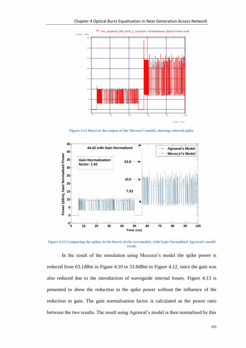
Chapter 4 Optical Burst Equalisation in Next Generation Access Network
105
Figure 4.12 Burst at the output of the Mecozzi's model, showing reduced spike.
Figure 4.13 Comparing the spikes in the bursts of the two models, with Gain Normalised Agrawal's model
result.
In the result of the simulation using Mecozzi’s model the spike power is
reduced from 63.1dBm in Figure 4.10 to 33.8dBm in Figure 4.12, since the gain was
also reduced due to the introduction of waveguide internal losses. Figure 4.13 is
presented to show the reduction in the spike power without the influence of the
reduction in gain. The gain normalisation factor is calculated as the power ratio
between the two results. The result using Agrawal’s model is then normalised by this
sim_argarwal_BM_test4_2_compare: Instantaneous Optical Power at b55707, Bursts_Entering_SOAs4, Run 1
0 20 40 60 80 100
0
5
10
15
20
25
30
35
Time [ns]
Power [mW]
0 10 20 30 40 50 60 70 80 90 100-5
0
5
10
15
20
25
30
35
40
45
Time (ns)
Po
we
r (d
Bm
), G
ain
No
rma
lis
ed
Po
we
r
Agrawal's Model
Mecozzi's Model
33.8
44.42 with Gain Normalised
22.6
7.53
Gain Normalisation
factor: 1.42

Chapter 4 Optical Burst Equalisation in Next Generation Access Network
106
factor so that it is comparable to the result using Mecozzi’s model. This shows that
using the variable step solver as well as considering the intraband effects can
improved the accuracy of the simulation result especially when rapid changes occur
in the signal.
Figure 4.14 Gain saturation characteristics of the two models compared with experiment result
The simulation result of Mecozzi’s model is almost identical to the physical
SOA measurement between -15dBm to 0dBm input power. Therefore, in the
unsaturated regime, the model re-produced the physical SOA results. The lowered
output power of Mecozzi’s model compare to Agrawal’s model is due to the
included waveguide internal loss. However, by using the new model the output
power saturation characteristics did not improve at the high input power, which
should have been the high saturation region of the SOA, at input powers above
0dBm.
The input and output power saturation characteristics of both SOA model
were measured and compared with the experimental booster SOA measurements in
Figure 4.14. The Mecozzi’s model showed similar trend to the physical SOA up to
about 5dBm input power. We expect the curve to flatten at 15dBm output power as
the SOA saturates then increase linearly again as the SOA will become transparent,
but the Mecozzi’s model saturates at about 10dBm output power then start increasing
-25 -20 -15 -10 -5 0 5 10 15-10
-5
0
5
10
15
20
Input Power (dBm)
Ou
tpu
t P
ow
er
(dB
m)
Mecozzi`s Model
Agrawal`s Model
Physical SOA measurements
Chapter 4 Optical Burst Equalisation in Next Generation Access Network
107
linearly. The saturation region of the Mecozzi’s model was too short compared to the
physical device, therefore, we will have to use lower input powers in our simulation,
so that we do not exceed the 5dBm input power to maintain validity of the model.
Although the SOA model is still not simulating the SOA characteristics
precisely, it is already capable of simulating the time-domain nonlinear effects of a
saturated SOA, this is important because these effects were not considered by
previous literature analysing similar methods of burst equalisation. The successful
simulation of these nonlinear effects will also provide the basis for the spectrum
analysis of the output signal from the saturated SOA, which will aid the subsequent
recover and detection of the original signal. Improvements can be made to the model
so that at the high saturation regime, the theoretical simulation matches the
experimental result more precisely.
4.3.1 Shortcomings and Adjustments to the SOA Model
The SOA models used above assumed a constant carrier lifetime at 200ps.
This assumption is valid for ultra-short pulse interactions (at less than 50ps pulse
width [75]) and the small-signal regime of SOA operation, i.e. when the SOA is
operating far from saturation, which is not the case here. In the case of pulse width
more than 50ps and less than 100ps, which is the main consideration for 10 Gb/s
access network, the saturation induced gain compression dominates. Therefore, the
response of the amplifier is mainly determined by the effective carrier lifetime,
which is carrier density dependent [75]. The effective carrier lifetime is governed by
two terms: the spontaneous emission rate and the stimulated emission rate.
To correctly model the experimental gain saturation characteristics, a carrier
density dependent carrier lifetime is required to replace the constant carrier lifetime

Chapter 4 Optical Burst Equalisation in Next Generation Access Network
108
parameter in the equations 4.7. The effective carrier density is given by equation
4.12 in [75].
( )
( )
(4.12)
Where
is the effective carrier lifetime;
N is the carrier density;
is the constant carrier lifetime;
( ) is the rate of recombination;
( ) represents the material gain;
is the differential gain, which is ( ) .
In a bulk SOA model, the differential carrier lifetime is simplified to equation
4.13, note that for spontaneous recombination, .
(4.13)
Therefore, when P the input power of the signal is low, will be very
small and can be neglected, so that the effective lifetime is the same as the constant
carrier lifetime. When the input power is high, the term is larger than one,
making the effective lifetime shorter, thus changing the gain at high input power.
The modification to the model was implemented in the simulation and the
result was compared with the experiment measurement of an SOA as shown in
Figure 4.15.

Chapter 4 Optical Burst Equalisation in Next Generation Access Network
109
Figure 4.15 Saturation characteristics of the models (New model has the effective carrier life time
implemented) compared with experiment results
The simulation results of both models are almost identical to the physical
SOA measurement between -15dBm to 0dBm input power. Therefore, at the
unsaturated regime, both models re-produced the physical SOA results. At high input
power, when the SOA reaches saturation, the carrier lifetime adjusted model’s gain
is saturating sooner than both Mecozzi’s model and the SOA device. The lower gain
saturation power of an SOA can limit the output power of the high powered burst
and amplify the low powered burst to achieve equalisation. The equalisation using
gain saturation is more clearly visible in the time domain result of the system
simulation.
4.3.2 Burst Equalisation Simulation Results
Using the simulation system configuration shown in Figure 4.9, and
implementing the carrier lifetime adjusted model, the time domain signals before and
after the equaliser is shown in Figure 4.16. The 5dB burst power level difference
were almost equalised and the effect of gain modulation at the leading edge of each
pulse can also be seen.
-25 -20 -15 -10 -5 0 5 10 15-10
-5
0
5
10
15
20
Input Power (dBm)
Ou
tpu
t P
ow
er
(dB
m)
New Model with effective carrier lifetime
Mecozzi`s built-in Model
Physical SOA measurements

Chapter 4 Optical Burst Equalisation in Next Generation Access Network
110
Figure 4.16 (left) The input signal to the limiting amplifier and (right) the output signal showing amplified
and equalised bursts.
Frequency chirping is produced when the phase modulation occurs together
with the signal distortion at saturation due to refractive index changes. The signal
frequency spectrum will be broadened by the chirped component of the signal. The
simulation reflects this as the spectrum of the input and equalised signals are
compared in Figure 4.17, the optical frequency shift is clearly visible after
equalisation by a saturated SOA. The broadening of spectrum is discussed further in
section 4.4.
Figure 4.17 Spectrums of the simulated input (green) and equalised output signal (red)
sim_argarwal_BM_test4_2_compare: Instantaneous Optical Power at b55333, Bursts_Entering_SOAs3, Run 1
0 20 40 60 80 100
0
0.025
0.05
0.075
0.1
0.125
0.15
0.175
0.2
Time [ns]
Power [mW]
sim_argarwal_BM_test4_2_compare: Instantaneous Optical Power at b55707, Bursts_Entering_SOAs4, Run 1
0 20 40 60 80 100
0
10
20
30
40
50
60
Time [ns]
Power [mW]
Before Equalisation Equalised Output
sim_argarwal_BM_test4_3_forpaper: Optical Spectrum at b55707, Bursts_Entering_SOAs4, Run 1sim_argarwal_BM_test4_3_forpaper: Optical Spectrum at b55333, Bursts_Entering_SOAs3, Run 1
193.38 193.4 193.42 193.44 193.46 -60
-40
-20
0
20
40
Frequency [THz]
dB [mW/THz]
After Equalisation:
Spectral Broadening
Before Equalisation:
No Spectral Broadening

Chapter 4 Optical Burst Equalisation in Next Generation Access Network
111
4.4 Spectral Broadening and Optical Filtering
4.4.1 The Mechanism of Spectral Broadening
When an intense optical signal is input to an SOA, the stimulated emission
process will cause the electron density in the conduction band and the signal gain to
decrease, the depletion and recovery of electrons are not instant, therefore, the
amplified optical signal at the output is distorted. During this modulation of the
electron density and gain, the refractive index of the SOA active region is modulated
at the same instance, therefore, frequency chirping occurs together with the signal
distortion in the time domain. The signal frequency spectrum will be broadened by
the chirped component of the signal in which the chirped signal will be frequency
shifted with respect to the un-chirped component of the signal. As a result of the co-
existence of chirp and signal distortion, suppressing the broadening in the frequency
domain is expected to reduce the signal distortion in the time domain as well. The
effect of filtering was observed in [76] when an input of continuous signal at 7Gb/s
is passed through a single SOA. It showed the BER performance of the unfiltered
output signal has degraded while for the filtered signal there was no degradation.
Instead of avoiding the nonlinear spectral broadening by avoiding gain saturation, it
is possible to reduce the signal distortion after the burst is levelled to further simplify
the equalisation system.
4.4.2 Simulated Performance Result with Optical Filtering
The SPM induced by gain saturation will lead to spectral broadening of the
pulse [42]. The use of narrow optical filtering to reduce the waveform distortion
induced by saturated SOA in optical switching was reported in [77]. It suggest that
by using an optical band pass filter, nonlinear patterning effects of ultra-short 2ps
pulses can be reduced from 2.5dB to 1.1 dB by detuning a 1nm optical band pass

Chapter 4 Optical Burst Equalisation in Next Generation Access Network
112
filter towards the side of spectrum that is opposite to the red-shifted chirped
components. In the context of burst equalisation system, the performance based on
the extinction ratio and BER changes by the applied filter need to be analysed.
Using the simulation model in section 4.3, the BER performance of the
equalised bursts were assessed, an optical filter was also implemented in the
simulation to show the differences in performance changed by optical filtering. The
result is shown in Figure 4.18.
Figure 4.18 Simulation estimated BER comparison between, equalised and filtered burst signal
The “loud” burst power were kept constant, the burst power differences is
made by reducing the power of the “soft” burst. As the power differences between
the two bursts increased, i.e. as soft burst weakens, the BER performance of the soft
burst gets better due to the less saturation induced distortion it had experienced. The
equalised high power burst is not error free but have a BER of , this is
because the higher burst power saturates the SOA and experiences saturation
induced time and frequency domain distortions as well as ASE noise. After the
signal passed through a narrow optical filter, with a cut-off frequency at 25GHz from
the centre signal wavelength (50GHz DWDM AWG), the loud bursts BER
performance is 5 orders of magnitude better the unfiltered case. The soft burst were
1.00E-13
1.00E-12
1.00E-11
1.00E-10
1.00E-09
1.00E-08
1.00E-07
1.00E-06
1.00E-05
1.00E-04
1.00E-03
1.00E-02
1.00E-01
1.00E+00
0 2 4 6 8 10 12
BER
Burst Power Difference (dB)
Equalised High PowerBurst
Equalised Low PowerBurst
Filtered and EqualisedHigh Power Burst
Filtered and EqualisedLow Power Burst

Chapter 4 Optical Burst Equalisation in Next Generation Access Network
113
initially free of error when its power is 2dB below the loud burst, when this low
power burst was getting too weak for detection, i.e. at 11dB below the loud burst, its
BER became .
4.5 Burst levelling Experiments
Experimental demonstration of this optical equalisation system with filtering
was also created. In order to find a filter with a 1nm bandwidth that also has a sharp
cut-off, several optical band-pass filters were measured and the selected filter
characteristic is shown in Figure 4.19.
Figure 4.19 Optical filter characteristics
Although a tuneable filter would be ideal in this case, the ones available do
not have a sharp enough cut-off. Therefore, arrayed waveguide (AWG) acting as an
optical filter that had a suitable sharp cut-off as well as within the wavelength range
of the filtering operation will be used in the experiment followed, for studying the
performance changes at near the filter cut-off wavelengths.
-100
-80
-60
-40
-20
0
1549 1550 1551 1552 1553
Po
wer
(d
B)
Wavelength (nm)
AOC Technologies AWG Ch4

Chapter 4 Optical Burst Equalisation in Next Generation Access Network
114
Figure 4.20 Burst equalisation experiment configuration block diagram
The burst levelling experiment configuration is shown in Figure 4.20. Two
lasers were gated by two outputs from a Field-programmable gate array (FPGA) to
simulate the burst from ONUs. Each packet is 125μs long, modulated by a data
signal from a 10Gb/s Pseudo random bit sequence (PRBS) generator, with a 500ns
guard time between the two bursts used to prevent overlapping. A 5dB optical
attenuator was placed after one of the laser output to simulate the optical path loss of
a distant ONU, thus providing the power difference between the two ONUs. The two
signals merged at the splitter/combiner just like they would in a real PON. The
isolator before each SOA was there to prevent noise from the SOA travelling back to
the laser. As described in theory, an optical filter was used to remove the chirped
component from the received signal. In a real network the filter can be custom made
or picked therefore, it would have been optimised for the network condition. A 10dB
attenuator was placed before the Digital Communications Analyser (DCA), because
the power from the output of the SOA was too high for its photodetector.
The combined effect of chirp in the SOA and fibre dispersion resulted in
spectrum broadening as shown in Figure 4.21. The broadening is a shift in frequency
of the chirped component of the signal away from the centre peak frequency which is
the un-chirped component of the signal. As demonstrated via simulation in section
4.4, it is expected that through the use of optical filter with a cut-off near the chirped
Laser 2
Laser 1
Data2
FPGA
&
Driver
CircuitAttenuator
Data1
Combiner
Isolator SOA
Pre-amp
SOAIsolator
Booster
DWDM
Filter
Attenuator
Measurement
Devices

Chapter 4 Optical Burst Equalisation in Next Generation Access Network
115
component, the distortions situated at the broadened part of the spectrum can be
reduced.
Figure 4.21 Signal Spectrum at the cascaded SOA input, after the preamp SOA and after booster SOA
amplification showing spectral broadening at SOA gain saturation
The aim of the experimental system is also to level the bursts and reduce the
non-linear distortions in the signal, together with the reduction of wideband ASE
noise due to filtering, this approach is also expected to increases the output signal’s
extinction ratio. Since the AWG filter’s pass-band wavelength is fixed, the source
laser is tuned instead to observe the performance change near the filter’s pass band
edge. Changing the laser diodes’ control temperature within a reasonable range
(25°C ± 15°C) is equivalent to tuning the wavelength. A tuning table was kept for
the relationship between the temperatures and the laser wavelengths. It is found that
the wavelength of the laser changed linearly with temperature in this range, the
temperature is therefore, translated into wavelength for the ease of analysis and
understanding. The wavelength of the laser was also tuned to measure the optical
spectrum, ER and BER near the cut-off of the optical filter, in the aim to find out
how the performance of the system is changed by the applied optical filtering.
After Booster
After Preamp
Input

Chapter 4 Optical Burst Equalisation in Next Generation Access Network
116
Figure 4.22 Power Spectrums of the amplified signal, the peak and the second highest peak were used as a
reference for the chirp and un-chirped components respectively
Figure 4.23 Comparison of filter response with ER and peak power differences as wavelength of the signal
is detuned to near the filter edge
The results in Figure 4.22 are spectrums of the output optical signal measured
by a spectrum analyser as the wavelength of the laser is tuned towards the optical
filter edge. The difference in peak power between the energies of the un-chirped
component reference peak and the energies of the chirped-side reference peak is
increasing towards the filter edge. The plot of these data is shown in Figure 4.23, it
compares the measured peak power differences and output signal extinction ratio
with the measured filter response.
1550.2 1550.4 1550.6 1550.8 1551 1551.2 1551.4-40
-35
-30
-25
-20
-15
-10
-5
0
Wavelength (nm)
Po
we
r(d
Bm
)
Optical Spctrums of the received signal
Power at energy peaks
1550.4 1550.6 1550.8 1551 1551.2 1551.4 1551.6 1551.8 1552-25
-20
-15
-10
-5
0
5
10
Wavelength (nm)
Pe
ak
po
we
r d
iffe
ren
ce
(d
B),
Ex
tin
cti
on
Ra
tio
(d
B)
Frequency response peak power differences
Filter response
Extinction ratio measured

Chapter 4 Optical Burst Equalisation in Next Generation Access Network
117
From Figure 4.23, it can be seen that the ER increased by 2dB near the edge
of the filter at about 1551.5nm, representing lower noise floor and reduced the signal
distortions at the chirped signal frequency. The ER then decreases because the
un-chirped signal frequency components have moved into the filter cut-off
frequency. The frequency peak power difference is plotted as a dash curve with X
marks in Figure 4.23, it is showing a significant increase in peak power difference
near the filter edge, representing the weakening of the broadened part of the signal
frequency response. The BER performance was also measured, it showed in Figure
4.24, where the BER performance reached 10-9
near the filter edge at about
1551.5nm. This is the same wavelength where the ER has shown the 2dB increase.
The performance decreased again sharply to 10-2
at 1551.7nm once the filter started
to suppress the un-chirped main signal.
Figure 4.24 BER performance at ONU wavelengths near the filter edge
4.5.1 Power Balancing the SOAs and Extinction Ratio Performance
In the previous experiment, no optical attenuator was placed between the
pre-amp and booster SOAs to limit the power going into the booster SOA. The pre-
1550.4 1550.6 1550.8 1551 1551.2 1551.4 1551.6 1551.8 1552-25
-20
-15
-10
-5
0
Wavelength (nm)
Filte
r p
ow
er
res
po
ns
e (
dB
)
1550.4 1550.6 1550.8 1551 1551.2 1551.4 1551.6 1551.8 155210
-9
10-8
10-7
10-6
10-5
10-4
10-3
10-2
BE
R

Chapter 4 Optical Burst Equalisation in Next Generation Access Network
118
amp output power should be just sufficient to saturate the booster SOA for burst
equalisation to occur. If that power is too high, it may cause un-necessary signal
distortion by operating the booster SOA further into the saturation region. Aside
from the distortion of the binary “1” of the signal pulse, high ASE noise and elevated
“0” floor also occurs at very high saturation, a near worst case example is shown in
Figure 4.25.
Figure 4.25 Equalised bursts and the eye diagram of one burst with elevated "0" floor and reduced
extinction ratio
The elevated “0” will have significant impact on the ER, which it is a ratio
between the power associated with the binary “1” and the power associated with
binary “0”. The two bursts at the input to the preamp SOA had high ERs at 12.87dB
(high power burst, laser 1) and 11.5dB (low power burst, laser 2). After the two
amplification stage, their unfiltered ERs were 4.43 and 6.36 dB for the high power
burst and the low power burst respectively. The lower power burst coming from laser
2 experience more amplification in the linear unsaturated gain region, therefore, its
ER was higher than burst from laser 1. In the following result in Figure 4.26, the
lower ER of the high power burst from laser 1 was measured, indicating the heavier
saturation induced distortion it experienced.
An attenuator was place between the preamp and the booster SOA for the
purpose of reducing the signal power entering the booster SOA. The ER of laser 1
was measured with wavelength tuning and the optical filter applied. The optical filter

Chapter 4 Optical Burst Equalisation in Next Generation Access Network
119
removed some excess wide band ASE noise, therefore, the filtered signal ER at
6.5dB was 2.1dB higher than the unfiltered case of 4.43dB, with 0dB attenuation.
Figure 4.26 Extinction Ratio at different losses when the attenuator is placed between preamp and booster
SOA
Similar ER increases that were observed as the results shown in Figure 4.23,
as the wavelength was tuned from the centre of the filter pass band to the filter band
edge. The ERs measured at various levels of power balancing attenuation is shown in
Figure 4.26. Lowering the signal power by 3.6dB after the preamp SOA have
increased the ER by 1dB. However, the ER increase became less significant at <
0.5dB, if the signal power is attenuated by 5.6dB or higher. Care must be taken not to
attenuate the signal power too much as this will lead the SOA to operate out of the
saturation region.
4.6 Conclusions
The near-far power difference problem of the upstream PON burst-mode
transmission results in fluctuating burst-by-burst power being received at the OLT.
An all-optical solution, including the use of a saturated SOA as a limiting amplifier
5
6
7
8
9
10
11
1550.4 1550.6 1550.8 1551 1551.2 1551.4 1551.6 1551.8
Exti
nct
ion
Rat
io (
dB
)
Wavelength (nm)
ER at 3.6dB attn ER at 5.6dB attn ER at 7.6dB attn
ER at 9.6dB attn ER at 0 attn
Chapter 4 Optical Burst Equalisation in Next Generation Access Network
120
to level the burst power was studied. Sample based dynamic SOA models that can be
used with OptSim were developed. In contrast to previous work in this area, our
studies considered not just the saturation induced non-linear gain but also the
saturation induced frequency distortions in the SOA. Two mathematical theories of
the saturated SOA were implemented as MATLAB coded blocks in OptSim. The
comparisons of simulation results show that Mecozzi’s model implemented using a
variable step size solver and added internal loss gave better time domain results,
represented by the much reduced gain spikes. At deep saturation, it was suggested
that using an effective carrier lifetime instead of a constant lifetime can give more
precise results at deeply saturated SOA. This parameter is important for accurately
simulating the time and frequency domain effects due to gain saturation. Burst
equalisation simulation results also showed that by using narrow (25GHz) optical
filtering, the BER performance as a result of the saturation induced distortion may be
increased by more than 5 orders of magnitude.
The idea of using SOA as a limiting amplifier was experimentally
demonstrated and shown to level the bursts that had a 5dB input power difference.
This burst power dynamic range translates to about 25km of fibre distance between
two ONUs assuming a 0.2dB/km loss SSMF. The dynamic range of the system at
5dB is still not high enough if long-reach access network is considered, systems that
provide more dynamic range, as well as additional features such as wavelength
conversion, is studies in Chapter 5. The method that uses sharp optical filter to
reduce the effect of spectral broadening caused by the non-linear effect in SOA was
suggested and tested, it showed 2dB increase in extinction ratio and 4 orders of
magnitude increase in BER performance near the filter edge. The power balancing
within the all-optical burst equaliser was also investigated, by using an attenuation of

Chapter 4 Optical Burst Equalisation in Next Generation Access Network
121
3.6dB placed between the two SOAs, the equalised loud burst ER is 1dB higher,
subsequent 2dB increases in attenuation increase the ER by 0.5dB or less. The key is
to set the attenuation value as low as possible to avoid unnecessary saturation
induced distortions and ASE noise, while the loud burst must be allowed to saturate
booster SOA for burst equalisation to occur.
Chapter 5 All-optical Processing In Wavelength Converting Optical Access Network
122
Chapter 5. Centralised Optical
Processing in a Long-reach
Wavelength Converting Optical Access
Network
5.1 Introduction
Wavelength division multiplexing (WDM) is widely acknowledged as a key
technology in the next generation of optical access networks, which will offer higher
line-rates, increased numbers of users, and extended reach, as well as being the most
energy efficient next generation access architecture [1, 4]. Thus, the evolution from
Gigabit Passive Optical Network (GPON) to Next Generation PONs (NG-PONs)
requires the integration of WDM in the already deployed GPON infrastructure.
Centralised optical processing may be placed at the intermediate exchange site in a
Wavelength Converting Optical Access Network (WCOAN) [13], allowing uncooled,
colourless transmitters to be used at the customer’s premises so that the access
Chapter 5 All-optical Processing In Wavelength Converting Optical Access Network
123
network is scalable and economically affordable to deploy. This exchange node will
provide all-optical signal processing as suggested in section 2.3.2, including
wavelength conversion and possibly signal regeneration, to consolidate the multiple
wavelength-drifting burst-mode data streams from each PON segment and convert
them to a set of fixed WDM wavelength channels for transmission over the backhaul
fibre.
In order to achieve the requirements for integrating CWDM PONs into a
single wavelength efficient WDM access backhaul, this chapter conducts a
characterisation and performance analysis of incorporating a SOA-MZI optical
regenerator as a Cross Phase Modulation (XPM) wavelength converter (WC) into a
PON with a DWDM backhaul. The all-optical processing functions of the SOA-MZI
and the proposed Centralised Optical Processing Unit (COPU) will be studied. An
experimental demonstrator of the wavelength conversion upstream system will be
built based on the proposed access network described in section 5.2. Then the BER
and transmission distance performance of the Cross Gain Modulation (XGM) and
XPM WC at 10Gb/s operation is compared in section 5.3, showing that the XPM
WC is more suitable for 10Gb/s PON. The SOA-MZI device is characterised in
section 5.4, the phase shifter voltage characteristic is shown enabling us to find the
operating point and lower loss input output ports of the SOA-MZI. Different
operating modes of the device are compared based on chirp and dispersion
dependent performance in long-reach application. The probe power range is also
characterised. The input power dynamic range (defined as the maximum range of
input power range that result in an error free BER) and wavelength drift tolerance of
the experiment system will also be measured and analysed in section 5.5. The need
to perform burst equalisation, wavelength conversion, input power dynamic range

Chapter 5 All-optical Processing In Wavelength Converting Optical Access Network
124
enhancement and signal regeneration eventually lead to the proposition of a
combination of devices which is the COPU, it will be experimentally studied in
section 5.6. Burst mode conversion performance is also studied and the dynamic
range of the COPU in burst mode was determined. The digital burst mode receiver
used in this experiment was developed by José Manuel Delgado Mendinueta [78],
whom also collaborated with us on the burst mode experiment. The BER
performances for the processed optical bursts at 0, 22, 40, 62km backhaul
transmission distance transmission distance was also presented.
5.2 Integrating PON with DWDM backhaul
Figure 5.1 Long-reach PON with centralised optical signal processing
Expanding the WCOAN architecture shown in Figure 1.2 in detail, the
integrated TDM-PON with DWDM backhaul access network upstream is shown in
Figure 5.1 where the network can be thought of as two sections: A passive feeder
network and an exchange site with backhaul transmission.
The first is a distributed fibre access network connecting each customer to the
local exchange. This is constructed in an identical fashion to traditional PONs with
distributed passive optical power splitters. The main issues in this section are the
high loss associated with the power splitting arrangement, the unlevelled optical
20km
20km
1.25Gbit/s
ONU
DWDM
Backhual
<60km
OLT
Electronics
Burst Mode
DataSimple Low Cost Tx
Standard Installed PON eg GPON or EPON
10Gbit/s
ONUBurst Mode
DataSimple Low Cost Tx
Next Gen PON
Multiple
Multirate
PONs
A
W
G
OLT
Electronics
Exchange Site
Core Site
Optical
Signal
Processing
Components
A
W
G

Chapter 5 All-optical Processing In Wavelength Converting Optical Access Network
125
burst power due to distance ranging and transmitted power tolerance of the ONUs,
and the wavelength drift of the ONUs laser sources because of temperature variation
for low cost, uncooled lasers used there. For every factor of 2 increase in the number
of customers served, >3dB loss is added to the loss budget. For a split factor of 256 a
loss of ~28dB with component tolerance is seen while at a split of 32 this is 18dB.
This, coupled with the demand for low cost/low power transmitters in the ONU
provided to the customer, means that the power available at the exchange site will be
restricted. Uncooled DFB lasers have a frequency variation with temperature of
~10GHz/K which is determined by the device expansion and the refractive index
change [79]. The acceptable temperature variation requirement will depend on the
location of the ONU (outside or in the customer premises), with the worst case,
outdoor scenario requiring operation over a temperature range of -20°C to 70°C.
This requirement means that any WDM channel spacing would be limited to at least
1THz.
Long-reach WDM access networks typically use active optical amplification
at the exchange sites to enhance transmission distance. At the exchange site, shown
in Figure 5.1, we introduce a COPU to consolidate multiple burst-mode data streams
with drifting wavelength and unequalled burst powers from each PON segment and
convert them to a set of stabilised WDM wavelengths with equalised burst-to-burst
power for transmission over the long-reach backhaul fibre, which may be dual fibres,
reusing current core or metro network fibres and may or may not include
amplification. The proposed COPU, shown in Figure 5.2, is composed of an optical
power equaliser followed by a wavelength converter.

Chapter 5 All-optical Processing In Wavelength Converting Optical Access Network
126
Figure 5.2 The centralised optical processing unit
The COPU is expected to meet three different requirements which are,
namely, wavelength conversion, optical burst power equalisation, and transmission
distance enhancement. The wavelength conversion process consolidates multiple
CWDM ONUs wavelengths onto a set of fixed DWDM wavelengths for efficient
backhaul transmission over a WDM optical link. Also, the unlevelled bursts coming
from ONUs at different distances from the exchange will need to be equalised to
reduce the receiver dynamic range requirement at the OLT. In addition, optical
bursts at the intermediate exchange site would need regeneration to have a higher
extinction ratio and possibly pre-chirping to enable dispersion tolerant transmission
required in the long reach scenario [24], which will increase the backhaul
transmission distance over an uncompensated link. The following sections will begin
by explaining why the move to XPM wavelength conversion is necessary.
5.3 Wavelength Conversion techniques for 10G-PON
The principal element in the COPU is the wavelength converter. A number of
wavelength conversion techniques are available, the most commonly used coherent
technique is four-wave mixing (FWM); the most common incoherent (cross-
modulation) techniques are XGM and XPM. The FWM wavelength conversion is
coherent as it preserves the phase information as well as the amplitude information,
making this conversion technique attractive as it is transparent to modulation format.
However, the FWM conversion efficiency between up- and down-conversion is
asymmetric and the efficiency can decrease sharply when the input signal
Probe λ
Burst Equaliser
Centralised Optical
Processing Unit
Pump λ
CWDM bursts
from multiple
ONUs
Large loud/
soft power
ratio
Wavelength
stabilised bursts to
the DWDM backhaul
Small loud/soft
power ratio
ONU
λ Converter
ONU
Chapter 5 All-optical Processing In Wavelength Converting Optical Access Network
127
wavelength shift is increased [15]. The conversion efficiency is defined as the ratio
between the converted signal power and input signal power [80]. As described in
Section 2.3, the uncooled ONU laser wavelength is not fixed and each customer’s
ONU wavelength may drift in the 20nm CWDM band. The wavelength of each ONU
is temperature dependent, thus a large mix of wavelengths maybe present at the
exchange at any one instance. It will be almost impossible to compensate for the
decrease in conversion efficiency if FWM was to be used as a wavelength converter
to map multiple CWDM signals on to a DWDM backhaul. In addition, FWM is
polarisation dependent which is not suitable for PON, because in PON the
distribution fibres are connected to more than 32 ONUs in the customer’s premise, it
will be extremely difficult and costly to maintain or control the polarisation for all
the fibre connections. Therefore, the remaining options are XGM and XPM
wavelength conversion techniques.
Previously, a network configuration was proposed making use of a
wavelength converter unit based on the XGM properties of SOA [13] for
consolidation of 2.5Gb/s PON systems. A demonstration of this XGM wavelength
converter was built in the laboratory, as shown in Figure 5.3. An input pump or data
signal modulates the gain of the SOA forming the XGM converter, which in turn
modulates the CW probe wavelength. The pump signal was filtered and the
remaining signal is at the probe wavelength carrying the inverse of the original data.
However, there exist some drawbacks of the XGM wavelength converter that
become an issue as the access network data rate is increased to 10Gb/s.

Chapter 5 All-optical Processing In Wavelength Converting Optical Access Network
128
Figure 5.3 Wavelength converter based on Cross Gain Modulation in SOA
Similar to the spectral broadening effect we observed in gain saturated SOAs
in Section 4.4, the gain saturation of the cross gain modulated SOA will result in
increased positive chirp [44]. The chirped signal increases the impact of dispersion
in long distance standard single mode fibre (SSMF) transmission, therefore, reducing
the maximum error free transmission distance of the signal. As the data rate is
increased to 10 Gb/s, the decreased pulse width means that the chirped signal eye
will be completely closed by dispersion after 11km of SSMF. Transmission at
10 Gb/s is therefore, more sensitive to dispersion than at lower data rates e.g.
2.5 Gb/s.
Figure 5.4 Comparing XGM and XPM wavelength converted signal at 2.5Gb/s and 10Gb/s data rate [13]
As shown in Figure 5.4, transmission of 100km is possible at 2.5 Gb/s, yet
the optical eye of the 10 Gb/s XGM wavelength converted signal is completely
SOA SOA
Backhual
Probe
CW Probe
XGM Wavelength
Converter
Input From
PON 2x2 Coupler
Data Pump
Data at Probe
Wavelength
a) 2.5Gbit/s after XGM
Conversion, No Fibreb) 2.5Gbit/s after 100 km
SMF
c) 10Gbit/s after XGM
Conversion (1530 nm)d) 10Gbit/s after 11 km
SMF

Chapter 5 All-optical Processing In Wavelength Converting Optical Access Network
129
closed after 11km of SSMF, which means the signal is not recoverable by the
receiver in the OLT without dispersion compensation.
An ideal wavelength converter should produce equal performance for
conversion of the input signal from short to longer wavelengths and vice versa.
However, this is not easily achieved. In XGM wavelength converters, the SOA gains
are not uniform across all operating wavelengths. The longer and shorter
wavelengths experience different gain variations with input power levels. Increasing
the input signal power causes the SOA gain to become saturated because of the
reduction in carrier injection from the bias current. The gain peak will shift towards
longer wavelengths as a result of the carrier depletion due to the reverse process of
the band-filling [81]. Therefore, when the CW pump is considered as a reference
wavelength, the longer wavelength will experience higher gain and therefore, it will
be easier for it to saturate the SOA. As a result of this effect, another drawback of the
XGM conversion scheme exists; extinction ratio conservation cannot be achieved for
both up and down wavelength conversion. Up converting the signal wavelength (for
example from 1550nm to 1560nm) will reduce the extinction ratio of the output
signal, as it is more difficult for the shorter input wavelength to saturate the SOA.
Therefore, the performance of the system will be reduced when converting to longer
wavelengths [82].
In order to overcome the extinction ratio degradation in XGM wavelength
converters and enhancing the extinction ratio and transmission distance of the
converted signal, XPM based on a dual SOA Mach-Zehnder Interferometer (SOA-
MZI) [83] can be used. The XPM WC using SOAs are considered the most effective
incoherent wavelength conversion technique because of its high conversion
efficiency, extinction ratio enhancement and negative chirp characteristics [84]. The

Chapter 5 All-optical Processing In Wavelength Converting Optical Access Network
130
XPM wavelength converters have previously been proposed previously for use in
WDM enabled core and metro networks [53, 85]. In the core network, the input
signal to the XPM converter is a continuous mode modulated signal with fixed
wavelength, constant power and reasonable extinction ratio. As a result of the cost
considerations for ONUs in access networks described in section 5.2, un-cooled,
wavelength not strictly defined lasers will be used in the ONUs, thus the temperature
dependent input signal wavelength to the XPM wavelength converter is no longer
precisely controlled. Burst mode signals are also expected instead of continuous
mode as is common in the core network. Wavelength and power differences between
bursts are also expected. Therefore, aside from wavelength conversion, the XPM
converter is expected to handle wavelength drifts and would ideally provide
extinction ratio improvement to the equalised bursts.
An integrated XPM wavelength converter was used in our experiment, as
shown in Figure 5.5. This scheme operates by using the input signal to modulate the
carrier density in the active region of the SOA, which in turn modulates the
refractive index. The result is phase modulation of the CW probe signal. The
interferometer configuration of the SOA transfers the phase modulation into
amplitude modulation due to the constructive and destructive interference depending
on the phase change. The advantage of using XPM is that the wavelength conversion
is not as wavelength dependent as XGM within the SOA operating range.
Up-conversion in XGM has a 6dB extinction ratio degradation, for both up- and
down- conversion, the penalty remained less than 0.5dB over a 26nm range [86],
therefore, it will be possible to conserve the extinction ratio when converting from
any wavelengths within the converter’s CWDM operating band. This greatly benefits
the ONU design requirement, because it enables wavelengths from low cost,

Chapter 5 All-optical Processing In Wavelength Converting Optical Access Network
131
colourless ONUs to be converted to a tightly controlled pump wavelength, allowing
the use of DWDM in the backhaul section of the PON while maintaining simplicity
for ONUs in the customer’s premises.
Figure 5.5 Wavelength converter utilising cross phase modulation, using the integrated SOA-MZI device
to perform XPM under non-inverting mode operation [82]
The XPM scheme also requires smaller gain variation to perform the
conversion. Hence, the effect of chirp is reduced and therefore, it allows
transmission at more than 10Gb/s and over longer distances. The ability to bias the
phase shifter in the XPM converter allows the interferometric SOA converter to
operate either on the positive or negative slope of the interferometer. The positive
slope of operation will generate negatively chirped non-inverting converted signals
which may enable transmission of 10Gb/s signal over long distances of standard
SMF. It is necessary to characterise the SOA-MZI device to find out the basic input
and output operating power condition required for good conversion performance.
Furthermore, the network conditions in access networks such as wavelength drift and
the “loud/soft” input burst powers are not the same as in core network where this
Probe λSOA
SOA
Pump λConverted Signal at Probe Wavelength
Inp
ut S
ign
al
Ca
rrie
r
De
nsity
Re
fra
ctive
Ind
ex
Co
nve
rte
d
Sig
na
lC
hirp
Wavelength Filter
Time

Chapter 5 All-optical Processing In Wavelength Converting Optical Access Network
132
device is typically used as a signal regenerator. It is also useful to take advantage of
the negative chirp that this device could generate to maximise backhaul transmission
distance using standard SMF, the characterisation can reveal the operating points that
can be used generate such negative chirp.
5.4 Characterisation of the SOA-MZI device
Figure 5.6 shows an internal schematic of the SOA-MZI device for the
following experiments. It was a prototype device supplied by CIP photonics
packaged as an integrated all-optical regenerator, which is used as a XPM
wavelength converter in this work.
5.4.1 Characterisation of the phase shifter voltage
The SOA-MZI has integrated thermo-optic phase shifters on each SOA arm.
When voltage is applied to a phase shifter, it heats up which results in a refractive
index change of the waveguide in one arm of the MZI [80], thus the phase bias point
of MZI can be electronically controlled. When the light from the upper and lower
arm of the SOA-MZI interfere in the output coupler, their phase difference causes
the output light to re-direct from one port to the other, this phase difference can be
adjusted by the phase shifter in either arm of the SOA-MZI. The result of the
adjustment can result in two modes of operation: the Non-inverting mode where the
output binary bits have the same polarity as the input, and the Inverting mode,
where the output binary bit is inverted with respect to the input. As illustrated in
Figure 5.6, a CW laser and two power meters were used to characterise the phase
shifter control voltage, giving us the operating points needed for the operating modes.

Chapter 5 All-optical Processing In Wavelength Converting Optical Access Network
133
Figure 5.6 Block diagram of the characterisation of phase shift control voltage
The CW laser source fed a -5dBm probe signal at 1555nm into port B, which
was coupled to both arms of the SOA-MZI device. Both SOAs are biased at the
typical operating current of 360mA, the top and bottom SOAs have an unsaturated
gain of 23.6dB and 20.1dB respectively at this bias values. Sweeping the phase
shifter voltage (VPS) from 0 to 25V showed that the largest power difference between
port F and G occurs at 15V. The probe polarisation is mechanically controlled via
the polarisation controller, in order to compare the effect of the CW probe
polarisations, a polarisation state was chosen based on a quantifiable value, in this
case the output power of port G. First, the polarisation controller of the input CW
tuneable laser was adjusted so that output power of port G was at its maximum,
8.43dBm. At the same time the power of port F then became -3.07dBm. At this
setting, the power difference between the two ports was the largest. Optical isolators
were also used at the connected input and output ports to prevent reflected light and
ASE noise from interfering with SOA operation. The bottom arm phase shifter was
grounded and the top arm phase shifter voltage was adjusted at 0.5V steps to obtain
the result in Figure 5.7.
SOA
SOA
SOA-MZI XPM Wavelength Converter
A
B
C
D
E
F
G
H
CW laser
Power
Meter 2
Power
Meter 1
Polarisation
controller
Phase
Shifter 2
Phase
Shifter 1
Ports Ports

Chapter 5 All-optical Processing In Wavelength Converting Optical Access Network
134
Figure 5.7 Output power at port F and G as a function of phase shifter voltage
The output ports F and G produced similar signal performance with a
complementary relationship as expected. The largest peak-to-null power differences
are 9.74dB and 9.61dB for port F and G respectively. The output power at port G is
1.5~2dB higher than port F at similar points in the plots such as the peaks and nulls.
We suspect this higher output power is due to the lower optical coupling loss of port
G. Therefore, in all future works port G will be used to ensure the converted signal
power is as high as possible.
When a 10Gb/s data signal was fed into port H, with VPS set on the rising
slops, i.e. VPS = 11.2V or 20.7V, a non-inverted output signal was observed at port
G. On the other hand, the inverted signal was observed when the phase controller
voltage is biased on the falling slope, that is when VPS = 16.6V or 24.1V.
It is observed that the SOA-MZI device is sensitive to changes in the probe
signal polarisation. Considering an opposite polarisation state, where the input probe
polarisation controller was adjusted so that at VPS = 15V, the output power of port G
was at its minimum, 2.35dBm, then the corresponding power of port F became
4.97dBm. The top arm phase shifter was adjusted at 0.5V steps again to produce
Figure 5.8.
-4
-2
0
2
4
6
8
10
0 5 10 15 20 25 30
Ou
tpu
t P
ow
er (
dB
m)
Phase Shifter Voltage of top arm (Volt)
Output Power @ F
Output Power @ G

Chapter 5 All-optical Processing In Wavelength Converting Optical Access Network
135
Figure 5.8 Output power at port F and G as a function of phase shifter voltage, with a opposite
polarisation state
As a result of the polarisation change, the port F and G output power peaks
and nulls are reversed, but with a reduced power difference between the peak and
null powers. The new peak-to-null power is 6.16dB and 5.65dB for port F and G
respectively. Also, the peaks and nulls undergo a shift to the right on the x-axis. In
this characterisation only one CW source is used, therefore, the peak-to-null power
difference is the maximum change in output power caused by the refractive index
change in the phase shifters. When the peak-to-null power difference is decreased, it
can be expected that, in the opposite polarisation state, the maximum amplitude
change as a result of the SOA cross-phase modulation will also decrease. Therefore,
at VPS = 15V, the 1st polarisation state where the power of the port G is highest is
expected to be the best polarisation state for port G, which makes the opposite
polarisation, where the power of port G is lowest, the worst case polarisation state.
The effect on wavelength converting performance of the best and worst
polarisation state can be measured. When a 10Gb/s, 1551.7nm pump signal was
connected to port H, it modulates the refractive index of the lower SOA. When the
converted signal is filtered at 1555nm it can be seen that its amplitude does depend
-4
-2
0
2
4
6
8
10
0 5 10 15 20 25 30
Ou
tpu
t P
ow
er (
dB
m)
Phase Shifter Voltage of top arm (Volt)
Output Power @ F,Opposite PolarisationOutput Power @ G,Opposite Polarisation

Chapter 5 All-optical Processing In Wavelength Converting Optical Access Network
136
on the probe signal polarisation states. As shown in Figure 5.9, the optical eye
height, ER, Q-factor were measured using the DCA. When the SOA-MZI was
operating in the non-inverting mode, the converted signal eye (A) with 1.5mW eye
height, 15.9 Q-factor and 15.1dB ER was observed for the best polarisation state. It
is much better than the quality of the eye (B) observed for the worst polarisation
state, which has 1.12mW lower eye height, 6.15 Q-factor and 13dB lower ER. For
the inverting mode at the best polarisation state, the converted signal eye (C) with
2.2mW eye height, 14.3 Q-factor and 6dB ER was observed. While the quality of the
eye (D) in the worst polarisation state has 1.2mW lower eye height, 9.37 Q-factor
and 2.3dB lower ER, showing that the polarisation dependency is not as strong as in
the non-inverting mode. The performance comparisons between the inverting and
non-inverting mode will be further investigated in the next section.
Figure 5.9 The eye of the non-inverting output signal, at opposite polarisation states.
The above results showed that it is possible to obtain non-inverting and
inverting mode operation in opposite polarisation states, thus the polarisation of the
A: Best polarisation state, Non-Inverting
VPS = 11.5V
B: Worst polarisation state Non-Inverting
VPS = 17.5V
C: Best Polarisation state Inverting
VPS = 16.6V
D: Worst Polarisation state Inverting
VPS = 13.8V

Chapter 5 All-optical Processing In Wavelength Converting Optical Access Network
137
probe signal need to be optimised so that the highest ER, eye height and Q-factor is
available for the converted signal. The term “worst polarisation state” used here is
only relative to the best polarisation state, where a clear converted signal can be
observed. The real “worst” polarisation condition will be when the two signals from
the top and bottom arm of the MZI structure are not aligned, in between the above
mentioned best and worst polarisations that completely corrupts the eye of the
converted signal.
As the CW probe is physically located with the SOA-MZI it could be
packaged together with the SOA-MZI device. Therefore, once the polarisation for
the probe is optimised it is not expected to change. In the following experiments, the
optimal probe polarisation will be used. After characterising the power and
polarisation operating points, the performance of the WC will also need to be
characterised, finding an optimal operating point for the WC.
5.4.2 Comparison between different operation modes
The SOA-MZI device is bi-directional, which allows the pump and probe
signal to be in either co-propagation or counter-propagation configurations. This
experiment aims to compare the wavelength conversion performance between the
co-propagating and counter-propagating setups, using different possible signal input
ports. Ports A and D are for co-propagating signals; E and H are for counter-
propagating signals, as shown in Figure 5.10. The non-inverting and inverting
operation performance of the SOA-MZI device was also compared.
Figure 5.10 Four possible propagation configurations with pump signal input ports at A,D,E,H
Probe Wavelength
SOA-MZI XPM Wavelength Converter
Converted Signal at Probe
Wavelength
A
BTunable Laser Source
C
D
E
F
G
H
Pump Signal
SOA
SOAPhase
Shifter
Phase
Shifter
Pump SignalPump Signal
Pump Signal
Co-Propagation Counter-Propagation
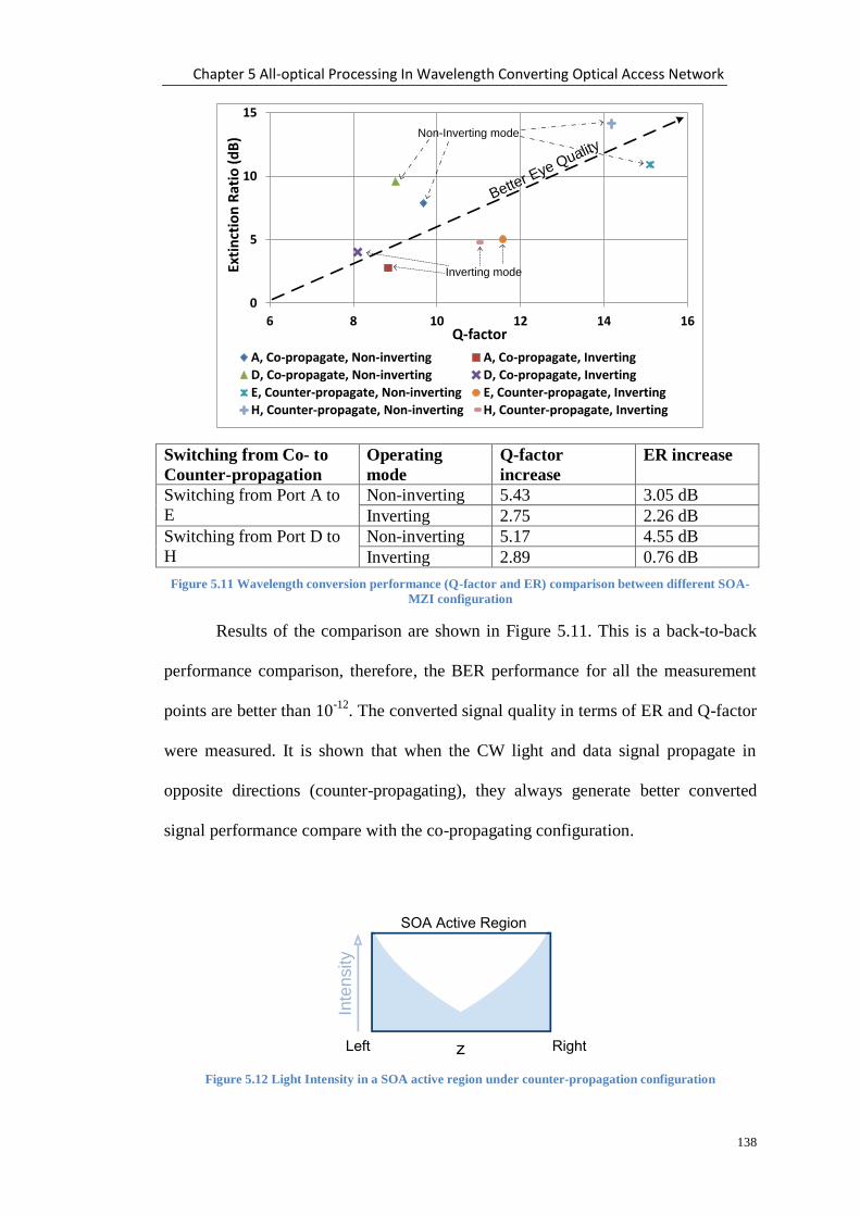
Chapter 5 All-optical Processing In Wavelength Converting Optical Access Network
138
Switching from Co- to
Counter-propagation
Operating
mode
Q-factor
increase
ER increase
Switching from Port A to
E
Non-inverting 5.43 3.05 dB
Inverting 2.75 2.26 dB
Switching from Port D to
H
Non-inverting 5.17 4.55 dB
Inverting 2.89 0.76 dB
Figure 5.11 Wavelength conversion performance (Q-factor and ER) comparison between different SOA-
MZI configuration
Results of the comparison are shown in Figure 5.11. This is a back-to-back
performance comparison, therefore, the BER performance for all the measurement
points are better than 10-12
. The converted signal quality in terms of ER and Q-factor
were measured. It is shown that when the CW light and data signal propagate in
opposite directions (counter-propagating), they always generate better converted
signal performance compare with the co-propagating configuration.
Figure 5.12 Light Intensity in a SOA active region under counter-propagation configuration
0
5
10
15
6 8 10 12 14 16
Exti
nct
ion
Rat
io (
dB
)
Q-factor
A, Co-propagate, Non-inverting A, Co-propagate, Inverting
D, Co-propagate, Non-inverting D, Co-propagate, Inverting
E, Counter-propagate, Non-inverting E, Counter-propagate, Inverting
H, Counter-propagate, Non-inverting H, Counter-propagate, Inverting
Inverting mode
Non-Inverting mode
Better E
ye Quality
Inte
nsity
Chapter 5 All-optical Processing In Wavelength Converting Optical Access Network
139
The reason for the differences in performance between the counter-
propagation and co-propagation configurations are due to the non-uniform
distribution of carriers in the SOA and the increasing amplification of the signal
towards one end of the SOA active region. Consider a SOA active region under the
counter-propagation setup, its light intensity profile will be similar to the illustration
in Figure 5.12. The CW probe is input from the left and amplified towards the right
side of the SOA, the amplified CW light depleted more carries towards the right side
of the SOA, leaving more free carriers at the left side of the active region. While the
counter-propagating data signal is input from the right and amplified towards the left
side of the SOA active region, which had more free carriers, these free carriers are
modulated by the amplified data signal. Since the refractive index modulation is
almost linearly dependent on carrier density modulation [87], the counter-
propagation is thus more efficient than the co-propagation setup for XPM
wavelength conversion. The amplified co-propagating signal can only modulate the
carriers that are depleted by the amplified CW light, therefore, it produces lower ER
and Q-factor than the counter-propagation setup. The following experiments all used
port H under counter-propagating configuration for best performance. Another
advantage of the counter propagating scheme is that it allows penalty free same
wavelength conversion. This is particularly useful for consolidating wavelengths
from multiple ONUs on to a single fixed wavelength, which could be at the same
wavelength as the probe. Since the input signal propagates in the opposite direction,
the input signal will not interfere with the output converted signal as it does in the
co-propagating mode.
Although the inverting mode of operation has 2dB higher average optical
power, the results showed that the non-inverting operation performs better producing

Chapter 5 All-optical Processing In Wavelength Converting Optical Access Network
140
wider eye openings and less patterning effect at the rising and falling edge of the
signal. This is evident by the higher Q-factor and Extinction Ratio (ER) of the non-
inverting signal in both the co- and counter- propagating configuration. It is seen that
the inverted output signals have higher output powers but are noisier than the non-
inverted signals.
5.4.3 Probe power characterisation for up and down wavelength
conversion
The probe source is a CW laser that provides the seed wavelength for the
wavelength conversion. The probe power cannot be too high as it will saturate the
SOAs, nor too low otherwise the ASE noise in the SOA will dominate, leading to a
low signal to noise ratio (SNR) of the converted signal that will decrease
performance. The experimental configuration is shown in Figure 5.13, with the probe
wavelength and power varying so that the optimum probe power dynamic range
could be measured. This characterisation will show the wavelength dependency of
the device, because in a DWDM arrangement, a range of probe wavelength spaced at
100GHz could be assigned as the probe wavelengths. There should not be significant
performance difference or penalty within the assigned probe wavelength range,
otherwise the device would not be suitable as a COPU. The probe power dynamic
range will show the probe power range required to achieve good BER performance
with in the assigned wavelength range. This characterisation was carried out in
continuous mode, since the probe CW source is expected to have constant power
during normal operation, the operating point deduced from this can also be used
under burst mode operation.

Chapter 5 All-optical Processing In Wavelength Converting Optical Access Network
141
Figure 5.13 Experiment setup for probe power characterisation
Figure 5.14 Spectrum of the converted signal, the blue dash line is the original pump (input data) signal at
1551nm
The pump data input signal was at 1551nm wavelength with a power
of -6.32dBm. The probe wavelength was tuned from 1545nm to 1565nm so that both
the up and down conversion of the pump signal was tested in this experiment. Figure
5.14 shows the overlapped spectrum of the converted signal output power at port G
of the SOA-MZI. The wavelength band from 1260 to 1280 nm was selected for the
XG-PON1 upstream [2], characterised by low chromatic dispersion. The prototype
device used in this experiment cannot operate at the XG-PON1 wavelength band
because it was initially designed to be used in the C Band (1530 to 1565 nm) of core
and metro networks. When using SOA-MZI devices in an actual XG-PON or
10GEPON system, they would need to be manufacture according to the XG-PON or
10GEPON wavelength band selection and standard.
Probe Wavelength
1545 to1565 nm
SOA-MZI XPM Wavelength Converter
Rx and ED
Converted Signal at Probe
Wavelength
A
BTunable Laser Source
C
E
F
G
H10Gbit/s Signal
Pump @ 1511nm
SOA
SOAPhase
Shifter
Phase
Shifter
D
1540 1545 1550 1555 1560 1565 1570-20
-18
-16
-14
-12
-10
-8
-6
-4
-2
0
2
Converted Signal Wavelength(nm)
Co
nv
ert
ed
Sig
na
l P
ow
er
(dB
m)
Original Input Signal
Converted Signal at 1545nm
Converted Signal at 1550nm
Converted Signal at 1555nm
Converted Signal at 1560nm
Converted Signal at 1565nm

Chapter 5 All-optical Processing In Wavelength Converting Optical Access Network
142
After 3dB loss in the optical coupler and another 3dB loss in the filter, the
peak power variation of the converted signal across the 1545 to 1565nm range is
small. The highest peak power is 0.1dBm at 1565nm probe wavelength and the
lowest is -1.2dBm at 1545nm. The largest difference in the probe peak power is
1.3dB between the 1545nm and 1565 nm wavelengths.
The probe power dynamic range was characterised based on BER
performance of the wavelength converted signal. The probe power dynamic range is
the maximum change in probe power without compromising the BER performance
of the wavelength converted output signal. A 10Gb/s PIN receiver and a Bit-Error-
Rate Tester (BERT) were used to measure the received signal BERs performance
after the wavelength conversion. At the input, a 10Gb/s optical signal was generated
from a DFB laser with an integrated EAM modulator, which, was modulated by a
231
-1 PRBS signal from the PPG of the BERT. The phase shifter voltage was
adjusted using the 1560nm probe wavelength as a reference. The optical power of
the probe was at -4dBm during the phase shifter voltage and polarisation controller
optimisation. The probe power was then varied from 0 to -8dBm for each probe
wavelength, Figure 5.15 shows a 3dB probe power dynamic range can be achieved
with an error free output signal (BER=10-12
) and with a fixed phase shifter voltage,
for all probe wavelengths from 1545 to 1565nm. A 4dB dynamic range can also be
achieved if the GPON target performance (BER=10-10
) is used. For individual
wavelengths, the dynamic range is 1 to 2dB wider due to a small change in
polarisation as the tuneable laser changes the wavelength. The 1560nm wavelength
used to optimise the polarisation has the widest, 5dB error free dynamic range.

Chapter 5 All-optical Processing In Wavelength Converting Optical Access Network
143
Figure 5.15 Probe power and wavelength optimisation without phase shifter adjustments
The minimum 3dB error free dynamic range allows at least 20nm wavelength
tolerance when the phase shifter voltage is fixed. Besides, the probe as a seed
wavelength source is expected to have stable power and is temperature controlled.
Therefore, a one-time polarisation, phase shifter voltage and probe power level is
required, and then the wavelength converter configuration can operate in its designed
wavelength band without re-adjustment.
If different probe powers are required, possibly due to network upgrade or
different network conditions, the phase shifters in the SOA-MZI device can be
electronically adjusted to optimise the probe power, giving an extended dynamic
range.
1.0E-12
1.0E-11
1.0E-10
1.0E-09
1.0E-08
1.0E-07
1.0E-06
1.0E-05
1.0E-04
1.0E-03
1.0E-02
1.0E-01
1.0E+00
-8 -6 -4 -2 0
BER
(lo
g)
CW Probe Power (dBm)
1545nm
1550nm
1555nm
1560nm
1565nm
3dB
4dB

Chapter 5 All-optical Processing In Wavelength Converting Optical Access Network
144
Figure 5.16 Extended probe power dynamic range by allowing phase shifter voltage adjustment
With a maximum phase shifter adjustments of ±1V from the VPS = 11.2V
non-inverting operation mode, the results in Figure 5.16 shows that the probe power
dynamic range can be widened to 6dB achieving error free operation (BER=10-12
)
and 8dB if the target BER is 10-10
. At -4dBm probe power, the tolerance to phase
shifter voltage change is the highest for any wavelengths within the 20nm band, the
phase shifter voltage can be ±0.7V from the fixed point (11.3V) for the system to
remain error free.
5.4.4 Chirp and Dispersion of the inverting and non-inverting modes
Figure 5.17 Schematic of a wavelength converted PON with un-amplified 20m and 40km backhaul
The next generation of access network with a long-reach backhaul can enable
aggregation of the access network and metro network over a larger area than today’s
standard PON. Therefore, long-reach backhaul transmission performance needs to be
studied as long distance transmission penalties can limit the maximum transmission
1.0E-12
1.0E-11
1.0E-10
1.0E-09
1.0E-08
1.0E-07
1.0E-06
1.0E-05
1.0E-04
1.0E-03
1.0E-02
1.0E-01
1.0E+00
-12 -10 -8 -6 -4 -2 0
BER
(lo
g)
CW Probe Power (dBm)
1545nm
1550nm
1555nm
1560nm
1565nm
6dB
8dB
Wavelength
Converter
Probe λ
20km 20~40kmRx ED
Pre-amp
ONU
1:16 splitter
-12dB
10Gbit/sAttenuator
λConvertedSOA

Chapter 5 All-optical Processing In Wavelength Converting Optical Access Network
145
distance of the PON upstream signal. The main penalties of long distance
transmission are due to optical power loss and dispersion in the SSMF. The
combined effect of chirp on the converted signal and dispersion can lead to pulse
broadening when the signal is transmitted through a non-dispersion-shifted (NDS)
fibre [82]. Figure 5.17 is the schematic of the experiment used to evaluate the
transmission distance penalty of the XPM wavelength converter. The signal from the
ONU at 1551nm is first transmitted over a 20km PON distribution section with the
splitter represented by a -12dB attenuator to simulate the loss of a 1:16 split ratio.
The probe wavelength is at 1560nm, on to which the data is converted. For the SOA-
MZI device used in this experiment, it was observed that the input pump power to
the SOA-MZI needs to be above -8.5dBm for the wavelength converter to produce
sufficient phase modulation that achieves error free converted signal performance.
There is also an extra 3dB loss in the input coupler and up to 1.8dB loss in the fibre
to device coupling, the -8.5dBm input signal power will be attenuated to -13.3dBm
as it reaches the SOA. The ONU signal power after transmission through 20km of
fibre and 1:16 splitter is already at -15.5dBm, which is lower than the minimum
required pump power of the SOA-MZI device, and therefore, an optical amplifier is
required to boost the signal power so that it is sufficiently high for the wavelength
converter.

Chapter 5 All-optical Processing In Wavelength Converting Optical Access Network
146
Figure 5.18 Non-inverting and Inverting mode 10Gb/s signal transmission distance comparison
Example eye diagrams of the received signals after 0, 20, 40km of backhaul
transmission are shown in Figure 5.18. The top row is the inverting operation mode
which induces positive chirp; and the bottom row is the non-inverting mode of
operation, which induces negative chirp [82]. The negative chirp is essentially red-
shifting on the leading edge of the pulse and blue-shifting on the trailing edge. In a
NDS fibre, because of fibre dispersion, the leading edge of the pulse travels slower
than the trailing edge, initially compresses the pulse before dispersion eventually
broadens the pulse to enable longer transmission distance. As discussed in section
5.3, the penalty as a result of the pulse broadening will be more severe as the bit rate
is increased to 10Gb/s, because the pulse width will decrease and the pulse
broadening will cause inter-symbol-interference at shorter transmission distance.
From Figure 5.18 a) to b), then to c), the eye closure due to pulse broadening
seen here is getting worse as the inverted output signal travelled through the fibre.
This is similar to the eye closure observed previously with the positively chirped
XGM wavelength converted signal that was transmitted through SSMF. However, in
XPM wavelength conversion, the inverting signal that travelled 40km can still have a
All at 10Gbit/s
a) Inverting mode (Positive Chirp),
0km backhaul SMF
d) Non-Inverting mode (Negative
Chirp), 0km backhaul SMF
b) Inverting mode (Positive Chirp) after
20km backhaul SMF
e) Non-Inverting mode (Negative
Chirp) after 20km backhaul SMF
c) Inverting mode (Positive Chirp),
40km of backhaul SMF
f) Non-Inverting mode (Negative
Chirp), 40km of backhaul SMF

Chapter 5 All-optical Processing In Wavelength Converting Optical Access Network
147
BER of 1.62x10⁻¹⁰
while the XGM converted signal only travelled 11km. This is
because the XPM conversion produced much less positive chirp than the XGM
conversion and therefore, the XPM converted signal is less sensitive to fibre
dispersion.
The non-inverting mode counterparts d) e) and f) show wider eyes and less
pulse broadening at each backhaul distance. In order to present a quantitative
comparison between the two operating modes, the power penalties for distances from
0 to 40km were measured. The power penalty is the additional power required to
maintain a BER of 10-10
which in this cases is mainly due to fibre loss, which
increases linearly with distance. The measurement of further than 40km transmission
distance is limited by the receiver sensitivity and the optical power of the converted
signal.
Figure 5.19 The power penalty in 0 to 40km backhaul distance transmission
As shown in Figure 5.19, for the same transmission distances, the positively
chirped inverting output signal resulted in larger power penalty than the negatively
chirped non-inverting signal, with the power penalty difference between the
inverting mode and non-inverting mode increased from 2.4dB at 20km to 6.5dB at
40km. The power penalty difference between the non-inverting mode and the fibre
0
2
4
6
8
10
12
14
16
18
0 10 20 30 40
Pen
alty
(d
B)
Transmission Distance (km)
Non-Invertingmode
Invertingmode
Loss of Fibre0.2dB/km
ONU (EAMmodulator)

Chapter 5 All-optical Processing In Wavelength Converting Optical Access Network
148
loss reference line remains <1.8dB from 20km to 40km. The power penalties of the
ONU, which has an integrated EAM modulator (denoted ONU only), were also
measured for reference purpose and there was only backhaul fibre between the ONU
and the receiver. This shows that the positive chirp generated by the SOA-MZI
device in inverting mode is larger than the ONU’s EAM modulator chirp which has a
chirping parameter of less than 1 [44]. 6.5dB extra power is required to boost the
inverted output signal at 40km to achieve the same BER performance. The XPM
wavelength converter output chirp was shown to be determined by the device
properties and the intensity of the input signal, regardless of input signal chirp
parameter [88]. Which means the converted signal chirp can still be negative under
non-inverting mode, even when the signal from the ONU carries positive chirp. As
for the non-inverting signal, the negative chirp allowed it to travel up to 50km and
still maintain a received BER below 10-10
.
The introduction of negative chirp as a result of biasing the SOA-MZI on the
positive slope of operation means that the converted signal pulse can travel longer
distances in a SSMF, because this type of pre-chirped signal is dispersion tolerant.
Figure 5.20. BER performance for 20km and 40km backhaul transmission distance
-14.5 -14 -13.5 -13 -12.5 -12 -11.5 -11
-3
-4
-5
-6
-8
-8
-9
-10
-11-12
Received Power(dBm)
log 1
0B
ER
20km to WC, 20km backhaul
20km to WC, 40km backhaul

Chapter 5 All-optical Processing In Wavelength Converting Optical Access Network
149
After transmission through a 20km distribution fibre, the signal is wavelength
converted, and then it travelled thought another 20 or 40km backhaul fibre. The
received non-inverting signal BER performance for the 20 and 40km un-amplified
backhaul are shown in Figure 5.20. Although the signal after 20km backhaul has
4dB higher average optical power, when they were attenuated to the same received
power level, the 40km backhaul has <0.5dB variation in BER performance compared
to the 20km backhaul transmission distance.
After 40km of backhaul SMF the non-inverted signal is still error free.
However, after 20km distribution fibre, the WC, and then a 60km backhaul the
signal power is reduced to -13.6dBm which is too low to maintain error free
performance. A booster SOA was required to amplify this signal resulting in the new
schematic shown in Figure 5.21 for long-reach transmission.
Figure 5.21. Schematic of a wavelength converted PON with 60km backhaul section, with an amplifier
before the receiver to boost the signal power level
Figure 5.22 BER performance for 60km backhaul transmission distance
Wavelength
Converter
Probe λ
60kmRx ED
λConverted
Booster
SOA
Attenuator
20km
Pre-amp
ONU
1:16 splitter
-12dB
10Gbit/sSOA
-12 -11.5 -11 -10.5 -10 -9.5 -9 -8.5 -8 -7.5
-3
-4
-5
-6
-8
-8
-9 -10-11-12-14
Received Power(dBm)
log 1
0B
ER
20km to WC, 60km backhaul with amplification

Chapter 5 All-optical Processing In Wavelength Converting Optical Access Network
150
After 60km backhaul, when the signal power is amplified, it is still error free,
but there is an error floor likely due to the ASE noise from the SOA used before the
OLT, the total transmission distance from the modelled ONU transmitter to the OLT
receiver is 80km.
This section has shown that the combination of negative chirp and dispersion
results in longer possible transmission distances. The chirp in a XPM wavelength
converter is small compared to the chirp generated in the XGM process, because
smaller gain modulation is required to produce a phase change of π radians which is
necessary for the modulation of the probe wavelength. The non-inverting mode of
operation requires the converter to operate on the positive slope of the interferometer
[82]. This mode of operation has the benefit of generating negative chirp. The pre-
chirped converted signal reduces the impact of dispersion and allows the signal to
travel a longer distance in a SSMF free of error. The chirp in the inverting mode of
operation is positive, therefore, the inverting signal, like the XGM converted signal,
is impacted more by dispersion after long distance SSMF transmission, and hence
the transmission distance for the inverted signal is limited.
5.5 Input Power Dynamic Range of the SOA-MZI Wavelength
Converter
The XPM wavelength converter operates by converting gain variations into
phase variations in one arm and then combining the signal from both arms, where the
signals interfered constructively and destructively depending on the phase difference
between the two arms. This makes the device very sensitive to input power
variations, because a small change in input power can change the phase of the signal
by more than π radians, thus changing the interference pattern which leads to an
inversion of the signal, causing large number of errors. Generally, XPM based WCs
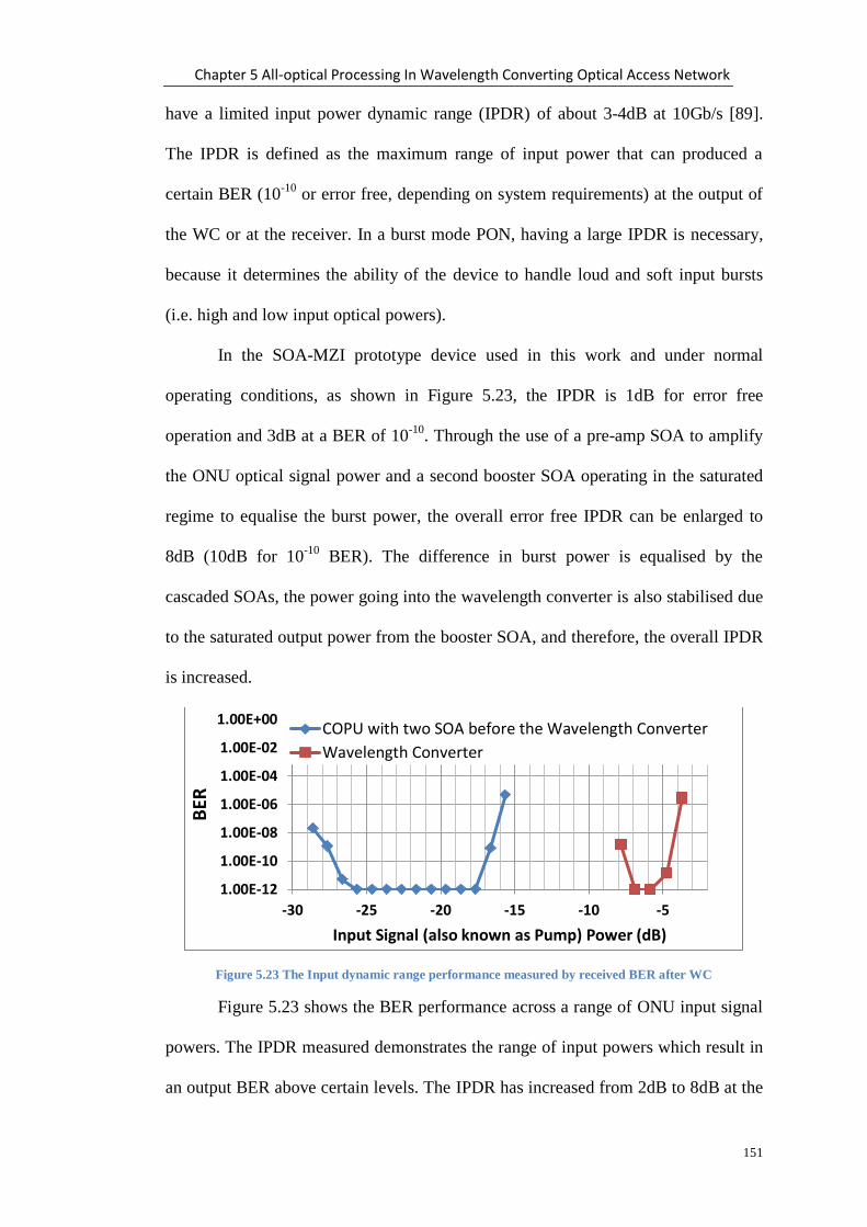
Chapter 5 All-optical Processing In Wavelength Converting Optical Access Network
151
have a limited input power dynamic range (IPDR) of about 3-4dB at 10Gb/s [89].
The IPDR is defined as the maximum range of input power that can produced a
certain BER (10-10
or error free, depending on system requirements) at the output of
the WC or at the receiver. In a burst mode PON, having a large IPDR is necessary,
because it determines the ability of the device to handle loud and soft input bursts
(i.e. high and low input optical powers).
In the SOA-MZI prototype device used in this work and under normal
operating conditions, as shown in Figure 5.23, the IPDR is 1dB for error free
operation and 3dB at a BER of 10-10
. Through the use of a pre-amp SOA to amplify
the ONU optical signal power and a second booster SOA operating in the saturated
regime to equalise the burst power, the overall error free IPDR can be enlarged to
8dB (10dB for 10-10
BER). The difference in burst power is equalised by the
cascaded SOAs, the power going into the wavelength converter is also stabilised due
to the saturated output power from the booster SOA, and therefore, the overall IPDR
is increased.
Figure 5.23 The Input dynamic range performance measured by received BER after WC
Figure 5.23 shows the BER performance across a range of ONU input signal
powers. The IPDR measured demonstrates the range of input powers which result in
an output BER above certain levels. The IPDR has increased from 2dB to 8dB at the
1.00E-12
1.00E-10
1.00E-08
1.00E-06
1.00E-04
1.00E-02
1.00E+00
-30 -25 -20 -15 -10 -5
BER
Input Signal (also known as Pump) Power (dB)
COPU with two SOA before the Wavelength Converter
Wavelength Converter
Chapter 5 All-optical Processing In Wavelength Converting Optical Access Network
152
reference BER of 10-12
(error free), while the IPDR is 10dB if a reference BER of
10-10
is used. This IPDR was achieved without any adjustment to the phase shifter
voltage or the bias current to the SOAs, the pre-amp and booster SOA bias current
were fixed at 200mA, their normal operating current for a typical gain of 21.7dB and
12dB respectively.
The gain saturation induced signal distortion starts to affect the amplified
signal performance at input signal powers above -10dBm, while the input power of
the signal becomes too deteriorated at -30dBm, so that the amplified signal do not
produce enough gain modulation to drive the cross phase modulation in the WC.
The advantage of this system, observed from the results of Figure 5.23, is
that the required power after the PON distribution section can be as low as -26dBm
for the wavelength converted signal to be error free, potentially allowing higher split
ratios such as 1:256 (24dB attenuation) or 1:512 (27dB attenuation), thus it will be
possible to serve a larger number of ONUs in the PON distribution section.
5.6 Performance of the Centralised Optical Processing Unit (COPU)
5.6.1 Gain and Saturation Characteristics
The input/output CW power characteristic of the COPU is shown in Figure
5.24. The output power saturates at 11.1dBm for the pre-amp SOAs when the input
power is high at -5dBm, the combined pre-amp and booster also saturates at
11.1dBm, but the cascaded SOAs begin to saturate at lower input power of -15dBm.
The polarisation dependent power penalty is less than 0.5dB in the pre-amp and
booster SOAs. For the whole COPU that contains two SOAs and a WC, the output
power saturates at 1.61dBm when the input power is -5dBm, but at -20dBm input
power, the output power already begins to saturate.

Chapter 5 All-optical Processing In Wavelength Converting Optical Access Network
153
Figure 5.24 COPU input and output power characteristics
The output power of the COPU mainly depends on the amplified probe
power, at the probe wavelength while the pump wavelength was cut-off by the
optical filter. The pump and probe power both saturate the SOA in the WC, while
there are also intrinsic losses of 3dB in each one of the SOA-MZI couplers, limiting
the overall input and output power level. For a PON with 1:32 split ratio, if the ONU
power is at 0dBm, the 15 dB loss in the splitter limits the COPU input power to a
maximum of -15dBm. An ONU signal from 15km away and going through a total
split ratio of 1:512 will be at -30dBm when it reaches the input of the COPU. For
this input power range of -15 to -30dBm, the output power ranges from 1dB to -6dB,
with a static COPU pump power polarisation dependent gain of 1dB. This
compression in the power range can be used to reduce the loud/soft ratio of the
optical bursts.
5.6.2 The two SOA saturation chirp and the SOA-MZI chirp
As shown previously in Figure 5.23, by using a pre-amp SOA to amplify the
ONU input signal power, and a second saturating booster SOA to equalise the signal
so that it has stable power at the WC input, the overall IPDR of the WC can be
-20
-15
-10
-5
0
5
10
15
-40 -35 -30 -25 -20 -15 -10 -5 0
Ou
tpu
t P
ow
er
(dB
m)
Input power to the COPU (dBm)
Pout after first SOA, Best polarisation
Pout after both SOA, Best polarisation
Pout after first SOA, Worst olarisation
Pout after both SOA, Worst polarisation
Pout Both SOA and WC, Best polarisation
Pout Both SOA and WC, Worst Polarisation

Chapter 5 All-optical Processing In Wavelength Converting Optical Access Network
154
enlarged. However, saturation of the booster SOA also produces un-wanted chirping
of the ONU signal. The chirp generated can caused severe signal distortion due to
the saturation induced self-phase modulation [42]. Overall, the power equaliser
degrades the extinction ratio and also exhibits patterning effects in dynamic mode.
On the other hand, these effects are compensated due to the regenerative properties
of the nonlinear transfer function of the SOA-MZI WC. This is because the transfer
function of the MZI structure has non-linear amplitude to phase response. The gain
induced phase shift and the output signal amplitude has a sinusoidal relationship.
When the induced phase shift is near π radians, the input amplitude noise induced
phase shift will be compressed [90]. Therefore, after the distorted signal has passed
through the WC it will be reshaped.
Figure 5.25 Relative SOA-MZI output amplitude as a function of induced phase shift in the SOA. The
amplitude noise is compressed when the phase shift is near pi radians [90].
Three example eye diagrams are presented in Figure 5.26 showing the shape
of the eyes at critical points in the system. The chirping in the cascaded SOA stage
causes severe signal gain distortion and amplitude noise at the input to the WC,
closing the eye as seen in Figure 5.26-(A). However, the distortion does not affect
the converted output signal (B), which is demonstrated by the fact that the Q-factor
has increased from 2.48 before the reshaping to 15.95 after the reshaping. The non-
inverting output signal still has negative chirp, allowing the signal to travel the 40km
backhaul while retaining a clear eye (C) and error free BER performance. We
Phase shift
MZ
I o
utp
ut a
mp
litu
de
π0
1
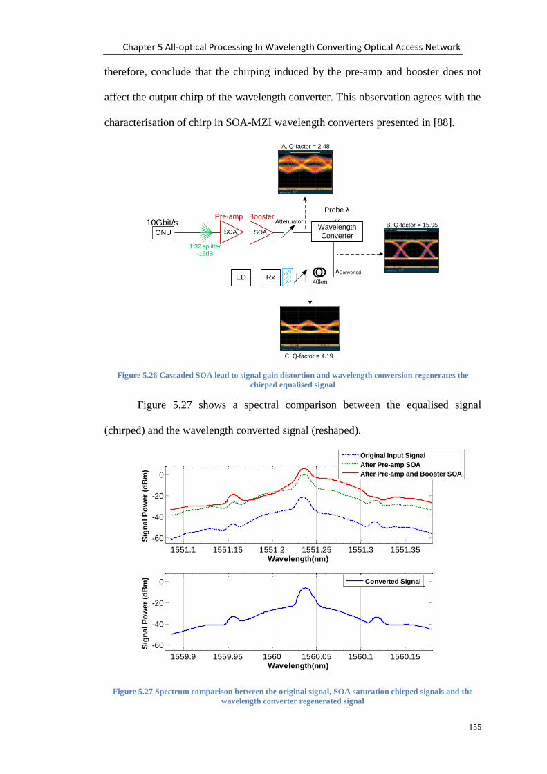
Chapter 5 All-optical Processing In Wavelength Converting Optical Access Network
155
therefore, conclude that the chirping induced by the pre-amp and booster does not
affect the output chirp of the wavelength converter. This observation agrees with the
characterisation of chirp in SOA-MZI wavelength converters presented in [88].
Figure 5.26 Cascaded SOA lead to signal gain distortion and wavelength conversion regenerates the
chirped equalised signal
Figure 5.27 shows a spectral comparison between the equalised signal
(chirped) and the wavelength converted signal (reshaped).
Figure 5.27 Spectrum comparison between the original signal, SOA saturation chirped signals and the
wavelength converter regenerated signal
Wavelength
Converter
Probe λ
40kmRxED
Pre-amp
ONU
1:32 splitter
-15dB
10Gbit/s
λConverted
SOA SOA
Booster
A, Q-factor = 2.48
B, Q-factor = 15.95
C, Q-factor = 4.19
Attenuator
1551.1 1551.15 1551.2 1551.25 1551.3 1551.35
-60
-40
-20
0
Wavelength(nm)
Sig
nal
Po
we
r (d
Bm
)
Original Input Signal
After Pre-amp SOA
After Pre-amp and Booster SOA
1559.9 1559.95 1560 1560.05 1560.1 1560.15
-60
-40
-20
0
Wavelength(nm)
Sig
nal
Po
we
r (d
Bm
)
Converted Signal

Chapter 5 All-optical Processing In Wavelength Converting Optical Access Network
156
The chirp induced by the cascaded SOA causes spectral broadening in the
input signal. The broadening is a shift in frequency of the chirped component of the
signal away from the centre peak frequency which is the un-chirped component of
the signal. As the signal passes through the SOA-MZI wavelength converter, the
output signal is wavelength converted as well as regenerated. The converted signal
spectrum shows that the spectral broadening and frequency shift was restored. If
wide deployment is required, there could also be cost benefits and performance gain
from the monolithic integration of the two SOAs and the SOA-MZI regenerator into
a single device for centralised optical processing. In the following experiment, the
term Centralised Optical Processing Unit (COPU) is used for this configuration.
5.6.3 IPDR and Backhaul Distance
Figure 5.28 Experiment setup for the reach assessment of IPDR
The effect of a long-reach backhaul on the IPDR is studied, which reflects the
maximum loud/soft power ratio of the signal entering the COPU. The distribution
fibre was not used, because dispersion may affect the signal quality resulting in a
lower IPDR. Backhaul SSMF distances of 0km, 22km, 40km, 62km were used in
this experiment, the IPDR at each backhaul distances was measured. In the result of
the IPDR measurement shown in Figure 5.29, the signal power loss in the 62km
un-amplified backhaul was approximately 13dB. The IPDR shrinks significantly, the
best BER performance was at 10-10
, observed at -20dBm input power.
0~62kmRx EDONU
1:32 splitter
-15dB
10Gbit/sλConverted
Probe λ
Pre-amp
SOA SOA
Booster
Pump λWavelength
Converter
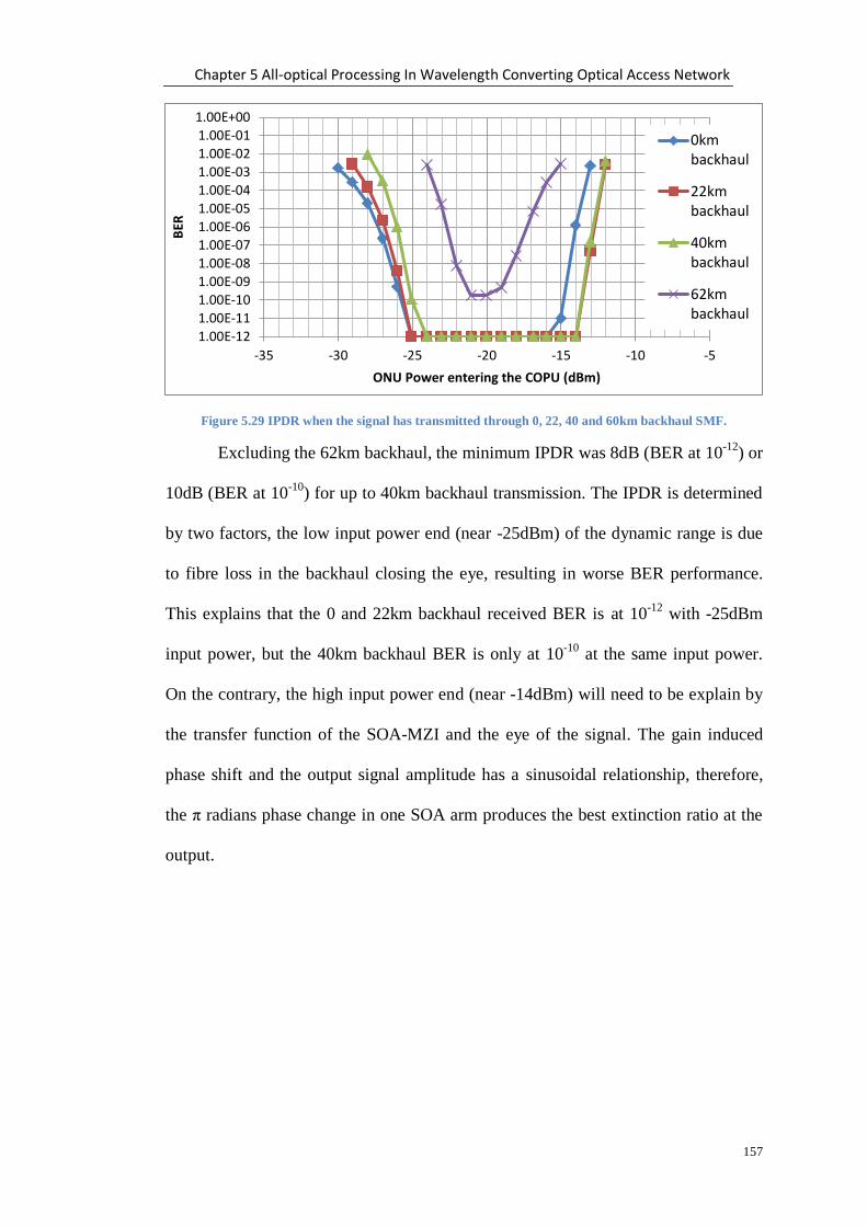
Chapter 5 All-optical Processing In Wavelength Converting Optical Access Network
157
Figure 5.29 IPDR when the signal has transmitted through 0, 22, 40 and 60km backhaul SMF.
Excluding the 62km backhaul, the minimum IPDR was 8dB (BER at 10-12
) or
10dB (BER at 10-10
) for up to 40km backhaul transmission. The IPDR is determined
by two factors, the low input power end (near -25dBm) of the dynamic range is due
to fibre loss in the backhaul closing the eye, resulting in worse BER performance.
This explains that the 0 and 22km backhaul received BER is at 10-12
with -25dBm
input power, but the 40km backhaul BER is only at 10-10
at the same input power.
On the contrary, the high input power end (near -14dBm) will need to be explain by
the transfer function of the SOA-MZI and the eye of the signal. The gain induced
phase shift and the output signal amplitude has a sinusoidal relationship, therefore,
the π radians phase change in one SOA arm produces the best extinction ratio at the
output.
1.00E-12
1.00E-11
1.00E-10
1.00E-09
1.00E-08
1.00E-07
1.00E-06
1.00E-05
1.00E-04
1.00E-03
1.00E-02
1.00E-01
1.00E+00
-35 -30 -25 -20 -15 -10 -5
BER
ONU Power entering the COPU (dBm)
0kmbackhaul
22kmbackhaul
40kmbackhaul
62kmbackhaul

Chapter 5 All-optical Processing In Wavelength Converting Optical Access Network
158
Figure 5.30 Received signal eye at high ONU power, on the right of every eye (A-F), the burst power
entering the COPU and the burst travelled backhaul distance is shown.
When the input signal power was above -15dBm, the SOA will be saturated
by the pump and resulting in a larger than π radians phase change which will reduce
the extinction ratio of the signal. As shown in Figure 5.29, the BER performance
gets worse as the input power to the COPU increases. At 0km backhaul, it can be
seen in Figure 5.30 (A and B) that at -14dBm input power the “1s” of the output
signal begin to reverse and there is significant noise in the “0s”, introducing errors.
As the signal propagates through 22km and then 40km of SSMF (Figure 5.30, C to
F), the loss in the fibre lowers the “0s” noise floor and dispersion broadens the pulse,
the signal eye is more open resulting in between 1 and 2 dB gain in BER
performance.
5.6.4 The impact of differential dispersion
Figure 5.31 Experiment to look at the differential dispersion introduced by difference in distribution fibre
distance
The ONU signal may go through different distances of PON distribution
SSMF before it reaches the COPU, with the different length of fibre introduces
A:
-14dBm,
0km
B:
-15dBm,
0km
C:
-14dBm,
22km
F:
-15dBm,
40km
D:
-14dBm,
40km
E:
-15dBm,
22km
Probe λ
20~40 km
DBMRx
Pre-amp
10Gbit/sSOA SOA
Booster
10Gbit/s
Centralised Optical
Processing Unit SOA
SOA
Pump λ
ONU
ONU
1:32 split
-15dB20km

Chapter 5 All-optical Processing In Wavelength Converting Optical Access Network
159
different amounts of dispersion. In this section the impact of dispersion is assessed
using continuous-mode operations.
Figure 5.32 IPDR difference between 0 and 20km distribution fibre distance
The results in Figure 5.32 show that the IPDR (ONU pump power range that
produced 10-10
BER) of the wavelength conversion system has been reduced from
12dB to 10dB with the addition of 20km distribution fibre, when the same 20km
backhaul is used. When no distribution fibre was used, the optical power loss
equivalent to the 20km fibre was compensated by 5.7dB attenuation of the input
signal. The upper limit of the IPDR has been reduced by 1dB and the lower limit of
the IPDR has been reduced by 1dB. This can be explained by the broadening in the
output signal eye shown in Figure 5.33 below. The IPDR with a 40km backhaul was
also shown, so that the total length of the SSMF travelled is the same as the 20km
distribution plus 20km backhaul case. When the distribution fibre distance is 0km,
extending the backhaul distance from 20km to 40km did not reduce the upper limit
of the IPDR while the reduction of the lower bound of the IPDR of 1dB is due to
loss in the fibre.
1.00E-12
1.00E-11
1.00E-10
1.00E-09
1.00E-08
1.00E-07
1.00E-06
1.00E-05
1.00E-04
1.00E-03
1.00E-02
1.00E-01
1.00E+00
-30 -25 -20 -15 -10 -5 0
BER
ONU Pump power (dBm)
No distributionfibre, 20kmbackhaul
20km distributionFibre, 20kmbackhaul
No distributionfibre, 40kmbackhaul

Chapter 5 All-optical Processing In Wavelength Converting Optical Access Network
160
Figure 5.33 Eye of the COPU output signal, A:0km distribution SSMF, B: 20km distribution SSMF
The pulse broadening is visible in the eye diagram of the wavelength
converted signals shown in Figure 5.33-B. Dispersion in the 20km PON distribution
section has reduced the COPU output signal Q-factor from 16.54 to 11.22, while the
shape of the output pulse is also broadened and the eye width reduced from 81.5ps to
71.9ps. When the ONU power is high, the output signal’s “0s” are shorter; when the
ONU power is low, the broadened signal is weaker because the peak of the pulse
amplitude is reduced by the broadening, resulting in a reduction in the received BER
performance.
5.6.5 ONU Wavelength Drift
Figure 5.34 Detailed experiment schematic for measuring the effect of input ONU signal wavelength drift
This section investigates the possible wavelength drift that occurs in an
uncooled ONU and its impact to the COPU and the WCOAN performance after long
A: COPU Output, 0km distribution fibre B: COPU Output,20km distribution fibre
Wavelength
Converter
Probe λ
Fixed
20km
40kmRxED
Pre-amp
MZI
10Gbit/s
λConverted
SOA SOA
Booster
Tunable
Laser
Pump laser
1554.52nm
-5dB
-2dBm
Pump λ Changes
1540~1560nm
Attenuator

Chapter 5 All-optical Processing In Wavelength Converting Optical Access Network
161
backhaul transmission. Building on the setup used in the previous section, a more
detailed schematic for this experiment is shown in Figure 5.34. Instead of modelling
the ONU using a temperature controlled DFB laser with integrated EAM modulator,
the ONU here is modelled by a tuneable laser with a Mach-Zehnder external
modulator so that we can simulate the wavelength drift of an un-cooled ONUs. The
tuneable wavelength ONU model was adjusted so that it has nearly identical eye
height and ER as the fixed wavelength ONU. The eye diagrams of the two modelled
ONU are shown in Figure 5.35.
Figure 5.35 The eye diagram of a fixed wavelength ONU and a tuneable wavelength ONU, the eye height
and ER were adjusted so that they are as similar as possible.
In order to ensure the wavelength tuneable ONU matches the fixed
wavelength ONU in performance, the MZ modulator bias voltage and the RF input
gain of the MZ modulator was adjusted so that their output power are the same, the
eye height difference is 5µW, the ER difference is 0.4dB and the Q-factor difference
is 3.54. The high level in the eye produced by the MZ modulator (B) is clearer than
the high level in the eye produced by the EAM modulator (A), this increases the
probability of detection a one, hence increasing the Q-factor. Isolators were again
used to prevent reflected light and ASE noise in the SOA from interfering with the
original signal and the SOA operation. The power of the ONU signal at the input to
the pre-amp SOA was changed while BER measurements were taken from the
receiver at the OLT. These measurements aim to find out the input power levels as
A: Fixed wavelength ONU,
EAM modulated 1551nm laserB: Wavelength Drifting ONU,
MZ modulated Tunable laser

Chapter 5 All-optical Processing In Wavelength Converting Optical Access Network
162
well as wavelengths at which the wavelength converted signal output can remain
error free, after a 40km backhaul. A -5dB attenuator was used to prevent the high
power signal after two stages of amplification from saturation the SOA-MZI
wavelength converter. When the tuneable laser is tuned to another wavelength, the
signal polarisation is slightly changed, since the MZ modulator depends on the signal
polarisation, the MZ modulator must be re-aligned each time the wavelength was
changed, before the start of each set of IPDR measurements. The wavelength
converter used in this experiment is a prototype device which is polarisation
sensitive to the pump signal. This polarisation dependency can account for up to 2
dB power penalty. Since polarisation insensitive SOA-MZI wavelength converters
are available [91], to minimise the effect of polarisation, the polarisation controller at
the input to the WC was optimised so that the output signal eye is at their best Q-
factor and ER.
Figure 5.36 The effect of pump signal wavelength drift on IPDR measured in terms of BER performance.
The result in Figure 5.36 shows that wavelength drift does not change the
system IPDR by more than 1dB when the pump signal wavelength is detuned to
±10nm from the starting wavelength at 1550nm. The IPDR is largest at the centre
1.00E-12
1.00E-10
1.00E-08
1.00E-06
1.00E-04
1.00E-02
1.00E+00
-23 -18 -13 -8 -3
BER
Attenuation of ONU power before amplification (dB)
1540nm
1550nm
1560nm

Chapter 5 All-optical Processing In Wavelength Converting Optical Access Network
163
wavelength of 1550nm, with a variation of 10dB in the power from the ONU
possible. The IPDR decreases to 9dB (10-12
BER) or 10dB (10-10
BER) as the
wavelength is tuned to 10nm away from the centre. This is because the centre
wavelength of 1550nm was used as a reference to setup the system, and is the point
at which the probe power was optimised for maximum pump power IPDR. Due to
the non-flat gain profile of the cascaded SOAs, a small shift in pump power at
±10nm wavelength can decrease the overall system IPDR. The phase shifter voltage
was also optimised for operation at 1550nm and remains unchanged throughout the
experiment, because under burst mode operation, the phase shifter voltage cannot be
changed manually at micro-second speed to re-optimise the system for each burst
power.
The scale of the ONU power stabilisation due to saturation in the SOAs can
be seen from the following result. Average pump power measurements were taken
before the pump signals were injected into the wavelength converter. In keeping with
the above IPDR measurements, the BER results here were measured at the receiving
end. After the signal was equalised in the cascaded SOAs, the 9dB (error free)
system IPDR shown in Figure 5.36 has now been reduced to less than 1.5dB, as in
Figure 5.37, which is less than the inherent 3dB IPDR of the WC.
Figure 5.37 Average pump power variation at the input to the WC
1.00E-12
1.00E-10
1.00E-08
1.00E-06
1.00E-04
1.00E-02
1.00E+00
7 7.5 8 8.5 9
BER
Average Pump Power after amplification (dB)
1540nm
1550nm
1560nm

Chapter 5 All-optical Processing In Wavelength Converting Optical Access Network
164
Figure 5.38 ASE noise profile of the pre-amp and booster SOAs formed equaliser
Another issue which must be considered is that the SOA ASE noise is not flat
across all wavelengths. Figure 5.38 shows that the SOA ASE noise is much higher
towards the gain peak at 1500nm. In the lower wavelength range (1540nm), the SOA
ASE noise is higher adding to the average pump power, shifting the pump power up
by 0.5dB. At the centre and higher wavelengths 1550nm and 1560nm, the ASE noise
power is 2 to 3dB less and therefore, the signal power dominates and the average
pump power is 0.5dB less.
5.6.6 Burst Equalisation and Wavelength Conversion
An experiment was built to test the burst equalisation and wavelength
conversion of the COPU using the standard PIN receiver. The setup is shown in
Figure 5.39.
Figure 5.39 Experiment setup for burst mode equalisation and wavelength conversion performed in a
COPU
-40
-35
-30
-25
-20
-15
1460 1480 1500 1520 1540 1560 1580 1600A
SE N
ois
e P
ow
er
(dB
m)
Wavelength (nm)
Operating Range
Probe λ
Pre-amp
SOA SOA
Booster
Centralised Optical
Processing Unit SOA
SOA
Pump λ
22 kmDCA
ONU
1:16 splitter
simulated by
-12dB
attenuator
10Gbit/s
λConverted
ONU
10Gbit/sFPGA
Gated
Laser
Driver
Combiner
-3dB
-6dB

Chapter 5 All-optical Processing In Wavelength Converting Optical Access Network
165
The ONUs were modelled by EAM modulated DFB lasers, with a 10Gb/s 231
PRBS pattern loaded onto both ONUs. The FPGA and gated laser driver together
generated alternating gating currents that turn the DFB lasers on and off, resulting in
alternating 125µs bursts with 500ns guard times between the bursts. A quick switch
to continuous mode operation is available, leaving either one of the ONU running at
continuous mode so that their BER or eye diagram can be monitored individually
using the BERT. In order to create the difference in burst power, a 6dB attenuator
was used at one of the ONU outputs. The ONU powers, when measured individually
in continuous mode, have 0dBm and -5.53dBm optical powers respectively. The
DCA was triggered using the gating signal, therefore, bursts are visible on the DCA
display, Figure 5.40 shows the ONU bursts at the combiner and the bursts observed
after the COPU output. It can be seen that their power differences are reduced, with
their signal powers measured in the continuous mode after 22km of backhaul fibre
being -4.86dBm and -5.40dBm. The power difference is reduced from 5.53dB to
0.54dB. Both converted signals showed an error free BER of 10-12
when monitored
under continuous mode using the BERT.
Figure 5.40 Bursts at the input and at the COPU output. Vertical scale are different, A:200µW/div,
B:500µW/div
A: Input Bursts B: Bursts at the COPU output

Chapter 5 All-optical Processing In Wavelength Converting Optical Access Network
166
Figure 5.41 Spectrum of the input signals and the converted signal at the COPU output, showing
wavelength conversion of the two signals to the same fixed wavelength
The combined spectrum showing the two input ONU signals and their
converted output signals are presented in Figure 5.41. It shows that the two ONU
signals at 1551.67nm and 1556.39nm wavelength were both converted to the same
probe wavelength at 1554.74nm. These spectrums were measured in the continuous
mode which reflects the “on” state spectrum of the burst. Under burst mode
operation, the laser power fluctuates and the spectrum will exhibit adiabatic chirp
generated during on/off laser switching. The 500ns guard time used between the
bursts allows on/off switching and laser power stabilisation, so that the power
fluctuations and adiabatic chirp do not introduce intensity noise during the burst
transmission.
5.6.7 Digital Burst-mode Receiver
The standard receiver used in the experiments so far is a DC-coupled PIN
receiver with clock synchronisation and data recovery in continuous mode operations
provided by the BERT. Under burst-mode condition, the fibre transmission
introduces optical delay of the signal, a burst-mode receiver or at least the burst
mode clock and data recovery function will be required to measure the burst BER. A
1551 1552 1553 1554 1555 1556 1557
-60
-50
-40
-30
-20
-10
0
Wavelength(nm)
Sig
na
l P
ow
er
(dB
m)
Input Signal A,
Input Signal B
Wavelength Converted Signal A
Wavelength Converted Signal B
1556.39nm
-26.09dBm
1554.74nm
-7.37dBm
1554.74nm
-7.37dBm
1551.67nm
-21.05dBm

Chapter 5 All-optical Processing In Wavelength Converting Optical Access Network
167
10Gb/s burst-mode receiver was not available for this experiment, but there is an
alternative solution, which is the digital burst-mode receiver (DBMRx) [78]
developed by José Manuel Delgado Mendinueta in the optical networks group at
UCL. The DBMRx is based on a DC-coupled PIN photodiode, a fast ADC, and has
digital clock and data recovery capabilities realised in software.
The receiver used a standard DC-coupled PIN photodiode and an integrated
trans-impedance amplifier (TIA) to convert the optical signal to electronic signals.
Then a Tektronix oscilloscope containing fast ADCs at 25GS/s was used to digitise
the signal for subsequent Digital Signal Processing (DSP) in MATLAB. The DSP
stage determines the line-rate and recovers the clock and data from the bursts [78].
5.6.8 Burst-mode System Performance
The implementation of the DBMRx changes the gating mechanism slightly.
Instead of using a continuous PRBS pattern in the PPG, a fixed length repeated
PRBS pattern containing two burst sequences 65536bits (6.6µs) long with 2048bits
(204ns) guard times was loaded on to the PPG. The PPG triggered the laser drivers,
which gate the laser. The fixed payload of the loud and soft burst will allow the
DBMRx to determine the errors in each burst and through post-processing determine
the BER of the individual bursts.
Although the length of the burst payload here is constrained due to the
limited PPG memory available, in a real NG-PON, the burst mode receiver will only
use less than 512ns information in the preamble and delimiter of a burst to set the
decision threshold, therefore, a 6.6µs burst length is sufficient to analyse the
performance of the system. At longer burst length, the threshold set should be the
same as the one set by a 6.6µs burst in out experimental system. In NG-PON, the
burst length can be more flexible than the GPON burst size and no longer limited to

Chapter 5 All-optical Processing In Wavelength Converting Optical Access Network
168
125µs per burst, in order to allow more efficient use of the upstream bandwidth.
XGPON bursts have a physical synchronisation block upstream (PSBu) followed by
a variable number of FEC codewords along with parity check bits, but the payload
size is not fixed, the last FEC codeword is shortened to ease the loss of bandwidth
caused by odd-sized bursts[2]. The 10G-EPON implementation is similar, it has a
laser synchronisation pattern and a fixed 66 bit burst delimiter pattern at the
beginning of each burst, followed by a start of frame preamble to signal the start of
the FEC codewords. At the end of the payload there is also a 66 bit block of burst
terminator pattern of alternating ones and zeros [92].
In the DBMRx, the DSP process in MATLAB compares the recovered data
from the ADC captured traces with the burst patterns in the PPG to determine the
detection threshold of the DBMRx and calculate the BER [78].
Figure 5.42 Burst-mode characterisation experiment setup with COPU and DBMRx
Figure 5.42 shows the experimental setup used to characterise the burst-mode
performance of the COPU. Two ONUs were modelled with two externally
modulated DFB lasers at different wavelengths (1553.5 and 1556.3nm), with an
extinction ratio of 14dB. In this COPU, the probe and pump signals are in a counter-
propagation configuration, as described in Section 5.4.2 this arrangement generates a
better signal performance in terms of higher extinction ratio and Q-factor. The probe,
onto which the upstream traffic is converted, was a CW laser at 1554.7nm As this is
a proof- of- concept experimental demonstration only commercially available C-
Probe λ
0~62 km
DBMRx
Pre-amp
10Gbit/sSOA SOA
Booster
10Gbit/s
Centralised Optical
Processing Unit SOA
SOA
Pump λ
ONU
ONU
-15dBmBurst
Pattern
Generator
& Gated
Laser
Driver-5dBm
~
-35dBm
(1dB Step)
A: Input Bursts
B: Output Bursts

Chapter 5 All-optical Processing In Wavelength Converting Optical Access Network
169
band devices were available in our laboratory. Wavelength conversion from 1.3 µm
to 1.5 µm using 1.3 µm SOAs has been previously demonstrated [68]. Both up and
down wavelength conversion were tested using this experimental setup and no
significant difference between the two was observed. Optical isolators were also
used at the ports to prevent reflected light interfering with SOA operation.
In real world applications the polarisation of the burst coming from the ONU
is random. The SOAs used in the equalisation stage have less than 0.5dB polarisation
dependent gain, but the SOAs inside this prototype SOA-MZI device had a stronger
polarisation dependent gain (PDG). The PDG changes the signal power in one arm
of the SOA-MZI, which affects the bias point of the WC and can result in an up to
2.5 dB dynamic polarisation penalty for the received BER sensitivity. It is expected
that a production grade SOA-MZI device will be used in the real system, which will
have an optimised SOA active region and is polarisation insensitive [91]. Therefore,
the bias point of a polarisation insensitive SOA-MZI device will not be affected by
the random polarisation of the ONU bursts.
The following procedure was used to adjust the ONU polarisation, i.e., the
WC bias point, to overcome the polarisation penalty of this prototype device. Two
bursts of -15 (loud) and -25 dBm (soft) were generated and then three COPU
optimisation cases, named A, B, and C, were chosen. These cases are illustrated in
Figure 5.43 for a backhaul transmission distance of 22 km, where the soft burst eye
was superimposed on the loud burst eye. The loud burst eye exhibits a nonlinear
distortion due to patterning-generated additional optical power before the SOA-MZI
sinusoidal transfer function, which contrasts with the characterisation of Figure 5.24,
where no eye overload is noticeable in static CW mode. In case A, the optical eye
diagram of the loud and soft bursts was equalised as much as allowed. Ideally, this
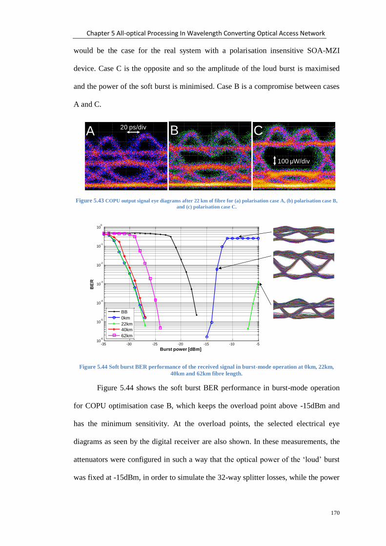
Chapter 5 All-optical Processing In Wavelength Converting Optical Access Network
170
would be the case for the real system with a polarisation insensitive SOA-MZI
device. Case C is the opposite and so the amplitude of the loud burst is maximised
and the power of the soft burst is minimised. Case B is a compromise between cases
A and C.
Figure 5.43 COPU output signal eye diagrams after 22 km of fibre for (a) polarisation case A, (b) polarisation case B,
and (c) polarisation case C.
Figure 5.44 Soft burst BER performance of the received signal in burst-mode operation at 0km, 22km,
40km and 62km fibre length.
Figure 5.44 shows the soft burst BER performance in burst-mode operation
for COPU optimisation case B, which keeps the overload point above -15dBm and
has the minimum sensitivity. At the overload points, the selected electrical eye
diagrams as seen by the digital receiver are also shown. In these measurements, the
attenuators were configured in such a way that the optical power of the ‘loud’ burst
was fixed at -15dBm, in order to simulate the 32-way splitter losses, while the power
A B C20 ps/div
100 μW/div
-35 -30 -25 -20 -15 -10 -510
-6
10-5
10-4
10-3
10-2
10-1
100
Burst power [dBm]
BE
R
BB
0km
22km
40km
62km

Chapter 5 All-optical Processing In Wavelength Converting Optical Access Network
171
of the ‘soft’ burst was swept from -5dBm to -35dBm in 1dB steps. For each step, 32
traces were captured and processed offline with MATLAB so as to obtain BER
measurements with acceptable confidence intervals. The back-to-back (BB) result in
Figure 5.44 indicates the DBMRx sensitivity in burst-mode operation and was
measured by connecting the burst-mode transmitter straight into the DBMRx. The
sensitivity is defined as the minimum soft burst power that produced a BER below
the 10-3
reference, which is the FEC limit. Implementing the COPU has contributed
to the digital receiver sensitivity by allowing 12dB lower input burst power to
achieve the same BER as the BB case, as well as performing wavelength conversion.
The sensitivity of the digital receiver is maximal for the 0km case and diminishes
with transmission distance due to fibre losses and dispersion. When the input burst
power is higher than -15dBm, the overshoot of the receiver is worse for the 0km case,
and improves with longer backhaul transmission distance. The SOA-MZI device
operating in non-inverting mode has the benefit of generating negative chirp. The
pre-chirped converted signal reduces the impact of dispersion, and so the results
show that the overshoot improves when fibre distance increases from 0km to 22km.
Three electrical eye diagrams shown in Figure 5.44 illustrate this effect at the
receiver side. For -9dBm burst power and 0km fibre transmission distance the
received eye is completely closed. By comparing this eye with the one at -13dBm
burst power we observe the fast eye degradation as input burst power increases, for
0km transmission distance. However, for -5dBm burst power and 22km of fibre the
eye is reasonably open, its BER is below 10-3
. On the other hand, the BER of the
loud burst was also monitored and it is always below the 10-3
FEC limit.
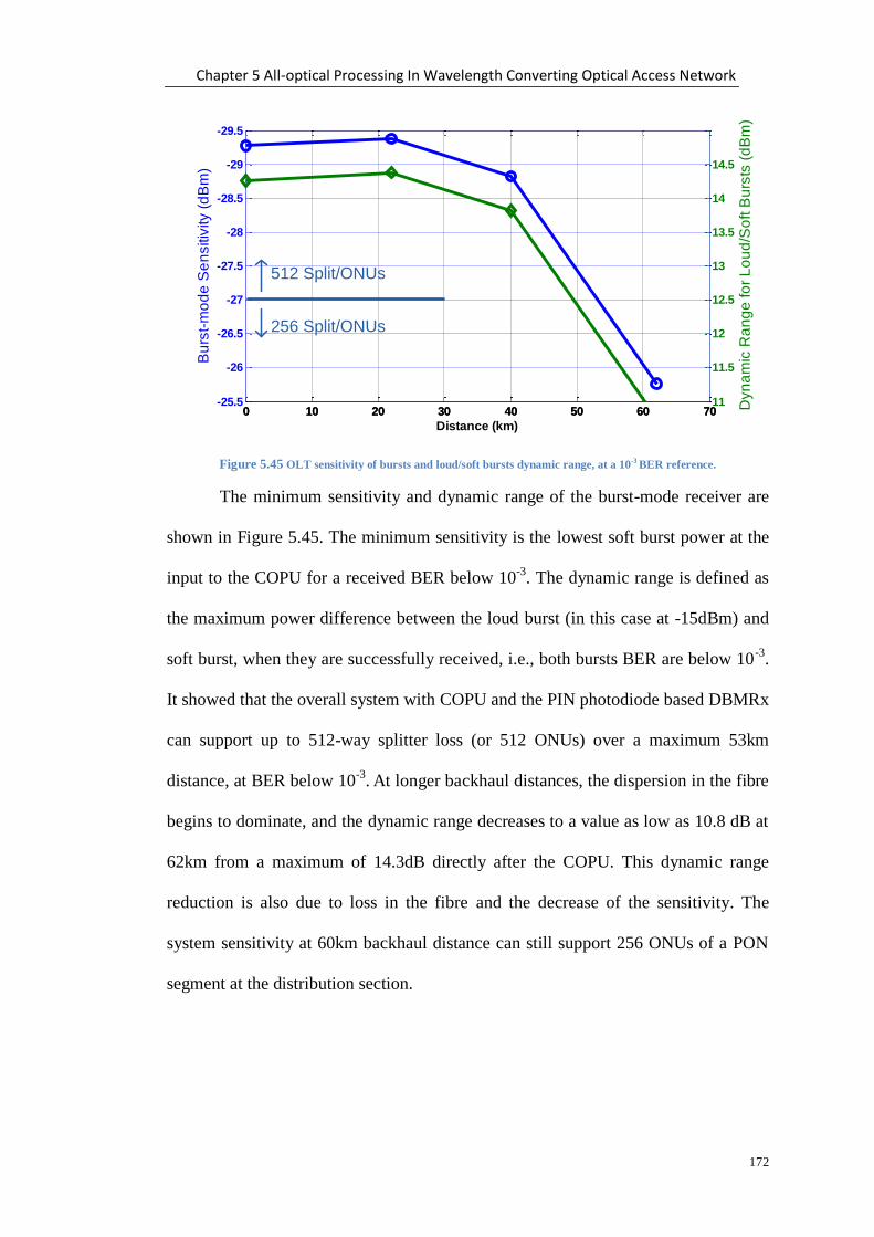
Chapter 5 All-optical Processing In Wavelength Converting Optical Access Network
172
Figure 5.45 OLT sensitivity of bursts and loud/soft bursts dynamic range, at a 10-3
BER reference.
The minimum sensitivity and dynamic range of the burst-mode receiver are
shown in Figure 5.45. The minimum sensitivity is the lowest soft burst power at the
input to the COPU for a received BER below 10-3
. The dynamic range is defined as
the maximum power difference between the loud burst (in this case at -15dBm) and
soft burst, when they are successfully received, i.e., both bursts BER are below 10-3
.
It showed that the overall system with COPU and the PIN photodiode based DBMRx
can support up to 512-way splitter loss (or 512 ONUs) over a maximum 53km
distance, at BER below 10-3
. At longer backhaul distances, the dispersion in the fibre
begins to dominate, and the dynamic range decreases to a value as low as 10.8 dB at
62km from a maximum of 14.3dB directly after the COPU. This dynamic range
reduction is also due to loss in the fibre and the decrease of the sensitivity. The
system sensitivity at 60km backhaul distance can still support 256 ONUs of a PON
segment at the distribution section.
0 10 20 30 40 50 60 70
-29.5
-29
-28.5
-28
-27.5
-27
-26.5
-26
-25.5
Bu
rst-
mo
de
Se
nsitiv
ity (
dB
m)
Distance (km)
0 10 20 30 40 50 60 7011
11.5
12
12.5
13
13.5
14
14.5
Dyn
am
ic R
an
ge
fo
r L
ou
d/S
oft B
urs
ts (
dB
m)
512 Split/ONUs
256 Split/ONUs

Chapter 5 All-optical Processing In Wavelength Converting Optical Access Network
173
5.7 Conclusions
In this chapter a new architecture to integrate multiple 10Gb/s CWDM PON
into a DWDM long-reach backhaul was introduced and described. The essential
element of this architecture is the Centralised Optical Processing Unit, which
contains a burst power equaliser stage and a wavelength conversion stage based on a
XPM WC. The WC’s power, polarisation and phase voltage bias were characterised.
It was found that by biasing the phase shifter, an inverting mode that generated
positive output signal chirp or a non-inverting mode that generated negative chirp
can be selected. The performances of the co- and counter- propagation modes were
also compared and it was concluded that counter-propagation generates 3dB higher
extinction ratio and 5.43 more signal SNR for this SOA-MZI based WC.
For the first time an experimental, upstream access network transmission
system using the XPM WC was demonstrated. The BER performance at 20km,
40km and 60km backhaul distances were compared and an error free (10-12
BER)
total transmission distance of 80km (20km distribution, 60km backhaul with optical
amplification) was achieved.
The overall Input Power Dynamic Range (IPDR) of the COPU was
characterised, the IPDR is larger than 10dB (10-10
BER) for transmission distances
up to 40km. The ONU wavelength drift within a 20nm wavelength window did not
change the IPDR by more than 1dB. However, the dispersion caused by a 20km
distribution fibre in the PON section can reduce the IPDR by 2dB due to pulse
broadening and power loss.
A proof-of-concept, full burst-mode long-reach wavelength converting
optical access network upstream that utilised the COPU was also experimentally
demonstrated for the first time. The BER performance at 22, 40, and 62 km backhaul

Chapter 5 All-optical Processing In Wavelength Converting Optical Access Network
174
distances were compared and a sensitivity penalty of -0.1dB, 0.6dB, and 3.6dB were
found, respectively. The same penalties were found in input burst dynamic range for
the aforementioned transmission distances. For this COPU that contained a prototype
SOA-MZI device, there is a less than 2.5dB overall polarisation-dependant penalty.
Chapter 6 Conclusions
175
Chapter 6. Conclusions
In this thesis, the design and performance aspects of the next generation
optical access network are investigated, they include interferometric noise in ring
based access networks as well as a novel intermediate stage optical processing
technology for the integration of multiple PON with a DWDM long-reach backhaul.
Theory, simulation and new experimental demonstrations were used to characterise
the performance in these 10Gb/s systems, it allows for a better understanding of the
operating range and merits of the proposed systems and their impact on performance.
Access network specific issues such as the temperature dependent source
wavelengths and burst-mode transmission have also been considered during the
investigations, the results obtained from these are significant, as similar techniques
used in the core network scenarios assumed fixed wavelength and continuous-mode
transmission.
WDM backhaul and wavelength stacking of multiple PONs is expected to be
used in next generation access networks, as well as optical amplifications, which can
Chapter 6 Conclusions
176
be used to enhance capacity and extend the network reach beyond 20km. In Chapter
2. The conditions of burst-mode transmission in passive optical network was also
describe in Chapter 2, along with the benefit of using all-optical processing, such as
burst equalisation, wavelength conversion and other techniques for achieving burst
mode levelling, access/metro network aggregations, DWDM backhaul integration
and reach extension.
In future ring based access networks with OADMs, interferometric noise may
arise from the interference of normal data signal and parasitic crosstalk, as a result of
the low cost OADM used. Previous core network studies in this area assume fixed
wavelengths, but in access, wavelength tolerance is a key factor and was considered
for the first time. In Chapter 3, current studies on the topic of burst equalisation
methods and the effects of interferometric noise (IN) in ring based access network
were reviewed. In the simulation and experiment presented in Chapter 3, the BER
performance characteristics for up to 0.08nm (10GHz) detuned wavelengths at
several interferer attenuation levels (18 to 40 dB) were shown. Using standard
10Gb/s PIN receivers with an 11GHz internal filter 3dB bandwidth, reducing the
interferer signal power or detuning its wavelength away from the data signal can
produced better BER performances in the received data signal. When the interferer
attenuation is at 20dB, 4 orders of magnitude better BER performance were observed
by detuning the interferer wavelength by 0.08nm (10GHz). The addition of an
electrical filter with a bandwidth of 7.5GHz after the receiver produced better
performance than using the receiver alone, it is most significant at > 5GHz detuned
frequencies. These observations lead us to simulate and develop a model to analyse
the BER performance characteristics at various electrical filtering bandwidths, while
also taking wavelength tolerance into account. This investigation showed by

Chapter 6 Conclusions
177
narrowing the receiver filter bandwidth and/or increasing the frequency detuning of
interferer, the amplitude and thus impact of IN is reduced. However, a less than
6GHz filter bandwidth can also lead to ISI, which will worsen the BER performance.
This is a significant and key conclusion for OLT design, it showed the impact of
receiver filter choice on BER performance, in ring access network with the presence
of IN. The simulation results were also compared and validated with the
experimental ones, the largest difference between the results is less than 1.5 orders of
magnitude of BER. The model is validated to be accurate in most results, except
when the distribution of filtered IN noise is half way between Gaussian and arc-sine
distributed, at 0.04nm (5GHz) detuned interferer wavelengths.
PON uses burst-mode transmission, the near-far ranging of ONUs produces
different power bursts in the upstream. In Chapter 4, the idea of using SOA as a
limiting amplifier in an optical burst equaliser was explained and demonstrated, in
order to ease burst-mode receiver dynamic range requirements for the OLT. SOA
models were developed and compared based on the ability to simulate real SOA
characteristics under normal and more importantly deep SOA saturation. It was
suggested that using an effective carrier lifetime instead of a constant lifetime can
give more precise results at SOA high saturation. A saturated SOA model was
created with carrier lifetime adjustments, which was validated by experimental
measurements. This new model was used to study the burst equalisation system’s
output signal BER performance, as well as the SOA saturation induced time and
frequency distortions in the equalised signal, which have not been previously studied
in this context. The experimentally verified model’s ability to simulate frequency
distortion alongside gain distortion is significant, as these effects are interlinked and
it showed that saturated SOA will chirp the equalised signal. Frequency chirping can
Chapter 6 Conclusions
178
harm the equaliser output signal performance, a better technique was implemented
and presented in Chapter 5 to tackle this issue, in order to reduce or eliminate the
SOA saturation induced gain and frequency distortions.
A proof of concept experimental dual SOA optical burst equalisation system
was presented for the first time, it levelled a 5dB difference in input burst power, this
is equivalent to 25km distance between two ONUs, which is 5km more than the
standard defined 20km maximum distribution fibre length. Optical filtering was
suggested to reduce the effect of spectral broadening caused by the non-linear effect
in SOA saturation. When the power difference between the two burst is at 2dB, we
observed 5 orders and 9 orders of magnitude increase in BER performance for the
filtered-equalised loud and soft power burst in simulation, respectively. As the soft
burst is attenuated to 11dB below the loud burst, the initially error free
filtered-equalised soft burst BER increase to 10-6
. A 2dB increase in extinction ratio
and 4 orders of magnitude increase BER performance was also observed in the
experiment, as the impact of chirped signal distortions was reduced by the optical
filtering. Power balancing the two SOAs by adding 3.6dB attenuation between them
was shown to increase the loud burst ER by 1dB, this is useful for high ONU input
powers that oversaturates the booster SOA.
In order to solve the signal distortion shortcoming of the two SOA burst
equalisation system as well as addressing the wavelength drift and extension of reach
in future access networks, Chapter 5 presented and first experimentally demonstrated
a new solution to integrate multiple up to 10Gb/s CWDM PON into a DWDM
long-reach backhaul through the use of a novel Centralised Optical Processing Unit
(COPU). This essential element contains a burst power equaliser stage followed by a
Chapter 6 Conclusions
179
wavelength conversion stage based on a XPM WC. This solution has the capability
to level burst power, stabilised wavelengths and extend transmission reach.
For the first time, a XPM based wavelength converter was demonstrated in a
burst-mode access network system that considers wavelength drift and wavelength
stabilisation, the performance of it at 20km, 40km and 60km backhaul distances
were compared. An error free 10Gb/s total transmission distance over 80km SSMF
was achieved owing to the pre-chirped WC output. Furthermore, the XPM WC was
also able to regenerate so that the spectral broadened and gain distorted signal from
the burst equaliser is restored for backhaul transmission. At the same time, the burst
levelling stage stabilises the input power to the XPM WC, therefore, its overall error
free Input Power Dynamic Range (IPDR) increased from 3 to 10 dB when measured
just after the COPU. The ONU wavelength drift within a 20nm window did not
change the IPDR by more than 1dB. However, the dispersion in 20km of distribution
fibre before the COPU can reduce the error free IPDR by 2dB due to pulse
broadening and loss. The significance of this result is that it showed that the IPDR of
the COPU is insensible to reasonale wavelength drift and it is only affected in the
extreme cases of dispersion, therefore, the COPU is robust enough to tolerate ±10nm
wavelength drift and supports ONU distribution distance up to 20km with a
maximum 3dB combined dynamic range penalty.
Continuous-mode and full burst-mode demonstration of a long-reach
wavelength converting optical access network architecture was presented and
demonstrated for the first time, incorporating this novel COPU. The BER
performance at 22, 40, and 62 km backhaul distances were compared. At 22km, loud
burst power and soft burst power entering the COPU at -15dBm and -29.3dBm were
both received and below 10-3
BER (FEC limit), which is equivalent to an input burst

Chapter 6 Conclusions
180
dynamic range of 14.3dB. In terms of split size and ONU numbers, this system
supports 512 ONUs at 53km SSMF backhaul distance and 256 ONUs at 62km
backhaul with a PIN photodiode based DBMRx, with dispersion compensation
techniques and higher sensitivity receivers, the backhaul distance can be increased
further. Sensitivity penalties of -0.1dB, 0.6dB, and 3.6dB were found, for 22, 40, and
62 km backhaul distances, respectively. The same penalties were found in dynamic
range for the aforementioned transmission distances. Since a prototype SOA-MZI
device was used in this SOA, there is a less than 2.5dB overall polarisation-
dependant penalty.
In conclusion, the aim to fully exploit existing ODN infrastructure by
consolidating multiple PON segments into a long-haul DWDM backhaul was
achieved and experimentally demonstrated, using intermediate optical processing
techniques. It has been shown that optical wavelength stabilisation, optical burst
equalisation and transmission distance enhancement can address next generation
access network design issues. Although the dual SOA burst equalisation alone has
limitations, when it is combined with an XPM WC in the COPU, together they can
level the incoming burst, thus reducing the dynamic range requirements of the OLT
receiver. This allows potential cost saving to operators deploying next generation
access networks. Through the use of DWDM in the backhaul, additional services can
be added to the backhaul of this network without changing the existing PON
distribution network. The ring access network performance in the presence of IN has
also been investigated, considering the wavelength tolerance of the system and filter
leakage in OADMs, specific to access network.

Chapter 6 Conclusions
181
6.1 Suggestions for future work
A number of possible further investigations are suggested as a result of the
work performed here.
A more advanced analytic model can be developed for the relationship
between BER performance and the filtering characteristics in the presence of
interferometric noise. This can extend the work in Chapter 3. In [93], it is found that
when the interferer are at unequal power the Gaussian approximation is not the ideal
model for the statistics analysis. Two particular BER assessment techniques based
on the Moment Generating Function (MGF) may instead be used, they are the
Saddlepoint Approximation [94] and the Modified Chernoff Bound [95].
The Further SOA model and parameters requires further adjustment and
refinement. It would be ideal to add the ability to simulate multiple wavelengths and
gain peak shift [81] due to laser pumping. If this can be achieved, the SOA model
will be able to simulate wavelength conversion in OptSim.
For the experimental work, some investigations were carried out to
investigate the IPDR of the SOA-MZI device in Chapter 5. If there is more time to
study this, other methods or combinations of methods to further increase the IPDR of
the COPU need to be found, thus allowing increased number of users in the
distribution network. The following table included the methods found in literature to
improve the input power dynamic range of the XPM wavelength converter.
Electronic control and all-optical methods are available. The cascaded SOA option is
similar to the burst equalisation in PON which was used in our experiment.
Methods Claimed
Improvement
on Dynamic
Range
Pros Cons References

Chapter 6 Conclusions
182
Electronic control
of phase arm
voltage/ SOA
bias current
5 dB/8 dB Low cost to
implement
Small dynamic range;
No directly available control
circuit because the control is non-
linear.
[89, 96]
Electronic control
of the SOA bias
current and phase
arm voltage
together
10 to 15dB Low cost to
implement
Only suitable for slowly varying
input power (~100ms)
Need to measure the phase arm
voltage and SOA bias current for
the optimum operating inverting
and non-inverting state.
[97]
Saturated EDFA 40dB Large
dynamic
range
Only suitable for slowly varying
input power, because of slow gain
recovery(~1ms), may not be
suitable for burst mode PON.
[89]
Electronic control
of SOA pre-
amplifier bias
current
28dB Large
dynamic
range, faster
gain
dynamics
than EDFA
High noise figure at high input
power (above -5dBm) because of
the corresponding low SOA bias
current (saturation power)
required for the phase adjustment
[89]
Integrated Pre-
amp
10dB No fibre-
chip
coupling
loss between
the pre-amp
and
wavelength
converter.
Require new fabrication or
purchase of new device;
Performance depends on the
device quality.
[98, 99]
Cascaded SOA
(similar to our
burst equalisation
setup)
20dB Moderate
dynamic
range
Non-linear effects in the SOAs
may lead to signal power penalty.
[100]
Control of SOA
gain through
external light
injection
(Tested
experimentally in
our setup, but did
not produced as
good result as the
SOA equaliser)
20dB Shortens the
carrier
lifetime
while
retaining the
saturation
output
power;
Less SOA
gain
distortions,
than the
SOA bias
current
control
method.
Requires optimisation for the
control light wavelength and
detailed power characterisation;
The control light power is non-
linearly related to the input power
and wavelength;
[84, 101]
The backhaul reach of the current system is at 62km, as this was an
unamplified and uncompensated reach which resulted in a good BER performance. It
is expected that this can be extended further, using APD receivers with higher

Chapter 6 Conclusions
183
sensitivity instead of the currently PIN photo-diode based receiver or further optical
amplification. Dispersion compensation fibre is another component that could be
used to extend the reach, which will need to be investigated if the required
components are available.
So far, our overall architecture did not consider more complex modulation
schemes and higher line-rate TDM due to the limited device availability for used in
experimental demonstrations. These can also be investigated in the future.
References
184
References
[1] K. Grobe, M. Roppelt, A. Autenrieth, J. P. Elbers, and M. Eiselt, "Cost and
energy consumption analysis of advanced WDM-PONs," Communications
Magazine, IEEE, vol. 49, pp. s25-s32, 2011.
[2] F. J. Effenberger, "The XG-PON System: Cost Effective 10 Gb/s Access,"
Lightwave Technology, Journal of, vol. 29, pp. 403-409, 2011.
[3] M. Hajduczenia and H. J. A. da Silva, "Next generation PON systems -
Current status," in Transparent Optical Networks, 2009. ICTON '09. 11th
International Conference on, 2009, pp. 1-8.
[4] J. i. Kani, F. Bourgart, A. Cui, A. Rafel, M. Campbell, R. Davey, and S.
Rodrigues, "Next-generation PON-part I: technology roadmap and general
requirements," Communications Magazine, IEEE, vol. 47, pp. 43-49, 2009.
[5] K. Kanonakis, I. Tomkos, T. Pfeiffer, J. Prat, and P. Kourtessis,
"ACCORDANCE: A novel OFDMA-PON paradigm for ultra-high capacity
converged wireline-wireless access networks," in Transparent Optical
Networks (ICTON), 2010 12th International Conference on, 2010, pp. 1-4.
[6] T. Kamijoh, M. Kashima, H. Tamai, M. Sarashina, H. Iwamura, and G. C.
Gupta, "CDM-technologies for next generation optical access networks," in
Optical Fiber Communication - incudes post deadline papers, 2009. OFC
2009. Conference on, 2009, pp. 1-3.
[7] D. Nesset, "Network operator perspective on WDM-PON systems and
applications," in Optical Communication (ECOC), 2011 37th European
Conference and Exhibition on, 2011, pp. 1-3.
[8] D. O. Committee. (2011, 15 Dec). FTTH Handbook 2011. Available:
http://www.ftthcouncil.eu/documents/Reports/FTTH-Handbook-2011-
V4.1.pdf
[9] K. Tanaka, A. Agata, and Y. Horiuchi, "IEEE 802.3av 10G-EPON
Standardization and Its Research and Development Status," Lightwave
Technology, Journal of, vol. 28, pp. 651-661, 2010.
[10] M. Hajduczenia, H. J. A. Da Silva, and P. Monteiro, "Development of 10
Gb/s EPON in IEEE 802.3av," Communications Magazine, IEEE, vol. 46,
pp. 40-47, 2008.
[11] A. Fu-Tai, K. Kyeong Soo, D. Gutierrez, S. Yam, E. Hu, K. Shrikhande, and
L. G. Kazovsky, "SUCCESS: a next-generation hybrid WDM/TDM optical
access network architecture," Lightwave Technology, Journal of, vol. 22, pp.
2557-2569, 2004.
[12] F. Saliou, P. Chanclou, F. Laurent, N. Genay, J. A. Lazaro, F. Bonada, and J.
Prat, "Reach Extension Strategies for Passive Optical Networks [Invited],"
Optical Communications and Networking, IEEE/OSA Journal of, vol. 1, pp.
C51-C60, 2009.
[13] D. P. Shea and J. E. Mitchell, "Architecture to integrate multiple PONs with
long reach DWDM backhaul," Selected Areas in Communications, IEEE
Journal on, vol. 27, pp. 126-133, 2009.
[14] R. P. Davey, D. B. Grossman, M. Rasztovits-Wiech, D. B. Payne, D. Nesset,
A. E. Kelly, A. Rafel, S. Appathurai, and Y. Sheng-Hui, "Long-Reach
Passive Optical Networks," Lightwave Technology, Journal of, vol. 27, pp.
273-291, 2009.

References
185
[15] P. Ossieur, C. Antony, A. M. Clarke, A. Naughton, H. G. Krimmel, Y.
Chang, C. Ford, A. Borghesani, D. G. Moodie, A. Poustie, R. Wyatt, B.
Harmon, I. Lealman, G. Maxwell, D. Rogers, D. W. Smith, D. Nesset, R. P.
Davey, and P. D. Townsend, "A 135-km 8192-Split Carrier Distributed
DWDM-TDMA PON With 2 x 32 x 10 Gb/s Capacity," Lightwave
Technology, Journal of, vol. 29, pp. 463-474, 2011.
[16] G. Williamson, "The challenge of the demand for access to the digital home -
The Journey to an Open Access Network," in IET Next Generation Networks
Conference, London, UK, 2007.
[17] S. Huan, K. Byoung-Whi, and B. Mukherjee, "Long-reach optical access
networks: A survey of research challenges, demonstrations, and bandwidth
assignment mechanisms," Communications Surveys & Tutorials, IEEE, vol.
12, pp. 112-123, 2010.
[18] D. E. A. Clarke and T. Kanada, "Broadband: the last mile," Communications
Magazine, IEEE, vol. 31, pp. 94-100, 1993.
[19] D. W. Faulkner, D. B. Payne, J. R. Stern, and J. W. Ballance, "Optical
networks for local loop applications," Lightwave Technology, Journal of, vol.
7, pp. 1741-1751, 1989.
[20] ITU-T, "Recommendation G.987: 10-Gigabit-capable passive optical
network (XG-PON) systems: Definitions, abbreviations, and acronyms," ed:
International Telecommunication Union, 2010.
[21] "IEEE Standard for Information technology - Telecommunications and
information exchange between systems - Local and metropolitan area
networks - Specific requirements Part 3: Carrier Sense Multiple Access with
Collision Detection (CSMA/CD) Access Method and Physical Layer
Specifications Amendment 1: Physical Layer Specifications and
Management Parameters for 10 Gb/s Passive Optical Networks," IEEE Std
802.3av-2009 (Amendment to IEEE Std 802.3-2008), pp. c1-214, 2009.
[22] D. Breuer, F. Geilhardt, Hu, x, R. lsermann, M. Kind, C. Lange, T. Monath,
and E. Weis, "Opportunities for next-generation optical access,"
Communications Magazine, IEEE, vol. 49, pp. s16-s24, 2011.
[23] D. P. Shea and J. E. Mitchell, "Long-Reach Optical Access Technologies,"
Network, IEEE, vol. 21, pp. 5-11, 2007.
[24] B. Cao, D. P. Shea, and J. E. Mitchell, "Wavelength Converting Optical
Access Network for 10Gbit/s PON," presented at the The 15th International
Conference on Optical Networking Design and Modeling, Bologna, Italy,
2011.
[25] M. Maier, "WDM Passive Optical Networks and Beyond: the Road Ahead
[Invited]," Optical Communications and Networking, IEEE/OSA Journal of,
vol. 1, pp. C1-C16, 2009.
[26] C. Bock, J. A. Lazaro, and J. Prat, "Extension of TDM-PON Standards to a
Single-Fiber Ring Access Network Featuring Resilience and Service
Overlay," Lightwave Technology, Journal of, vol. 25, pp. 1416-1421, 2007.
[27] J. Prat, V. Polo, J. A. Lazaro, F. Bonada, E. Lopez, B. Schrenk, M. Omella,
F. Saliou, Q. T. Le, P. Chanclou, D. Leino, R. Soila, S. Spirou, L. Costa, A.
Teixeira, G. M. Tosi-Beleffi, D. Klonidis, and I. Tomkos, "Demonstration
and field trial of a scalable resilient hybrid ngPON," in Optical
Communication (ECOC), 2011 37th European Conference and Exhibition
on, 2011, pp. 1-3.

References
186
[28] S. Dahlfort, "Comparison of 10 Gbit/s PON vs WDM-PON," in Optical
Communication, 2009. ECOC '09. 35th European Conference on, 2009, pp.
1-2.
[29] ITU-T, "Recommendation G.984.2 : 'Gigabit-capable Passive Optical
Networks (GPON): Physical Media Dependent (PMD) layer specification',"
ed: International Telecommunication Union, 2003.
[30] S. Chao, C. Lian-Kuan, and C. Kwok-Wai, "Theory of burst-mode receiver
and its applications in optical multiaccess networks," Lightwave Technology,
Journal of, vol. 15, pp. 590-606, 1997.
[31] T. Nakanishi, K. I. Suzuki, Y. Fukada, N. Yoshimoto, M. Nakamura, K.
Kato, K. Nishimura, Y. Ohtomo, and M. Tsubokawa, "High sensitivity APD
burst-mode receiver for 10Gbit/s TDM-PON system," IEICE Electronics
Express, vol. 4, pp. 588-592, 2007.
[32] H. Wessing, B. Sorensen, B. Lavigne, E. Balmefrezol, and O. Leclerc,
"Combining control electronics with SOA to equalize packet- to-packet
power variations for optical 3R regeneration in optical networks at 10
Gbit/s," in Optical Fiber Communication Conference, 2004. OFC 2004,
2004.
[33] B. C. Thomsen, B. J. Puttnam, and P. Bayvel, "Optically equalized 10 Gb/s
NRZ digital burstmode receiver for dynamic optical networks," Opt. Express,
vol. 15, pp. 9520-9526, 2007.
[34] A. V. Tran, C. J. Chae, and R. S. Tucker, "Optical packet power equalization
with large dynamic range using controlled gain-clamped SOA," in Optical
Fiber Communication Conference, 2005. Technical Digest. OFC/NFOEC,
2005, p. 3 pp. Vol. 1.
[35] R. Sato, T. Ito, Y. Shibata, A. Ohki, and Y. Akatsu, "40-gb/s burst-mode
optical 2R regenerator," Photonics Technology Letters, IEEE, vol. 17, pp.
2194-2196, 2005.
[36] W. Xing, Y. Su, L. Xiang, J. Leuthold, and S. Chandrasekhar, "10-Gb/s RZ-
DPSK transmitter using a saturated SOA as a power booster and limiting
amplifier," Photonics Technology Letters, IEEE, vol. 16, pp. 1582-1584,
2004.
[37] M. Zirngibl, "An optical power equalizer based on one Er-doped fiber
amplifier," Photonics Technology Letters, IEEE, vol. 4, pp. 357-359, 1992.
[38] C. R. Giles, E. Desurvire, and J. R. Simpson, "Transient gain and cross talk
in erbium-doped fiber amplifiers," Opt. Lett., vol. 14, pp. 880-882, 1989.
[39] D. P. Shea and J. E. Mitchell, "A 10-Gb/s 1024-Way-Split 100-km Long-
Reach Optical-Access Network," Lightwave Technology, Journal of, vol. 25,
pp. 685-693, 2007.
[40] H. Xiaobin, H. Weiping, and W. Jian, "Burst mode receiver based on SOA,"
in Optical Fiber Communication and Optoelectronics Conference, 2007
Asia, 2007, pp. 324-326.
[41] S. V. Pato, R. Meleiro, D. Fonseca, P. Andre, P. Monteiro, and H. Silva,
"All-Optical Burst-Mode Power Equalizer Based on Cascaded SOAs for 10-
Gb/s EPONs," Photonics Technology Letters, IEEE, vol. 20, pp. 2078-2080,
2008.
[42] G. P. Agrawal and N. A. Olsson, "Self-phase modulation and spectral
broadening of optical pulses in semiconductor laser amplifiers," Quantum
Electronics, IEEE Journal of, vol. 25, pp. 2297-2306, 1989.

References
187
[43] L. B. Kazovsky, Sergio; Willner, Alan, Optical Fiber Communication
Systems. Massachusetts: Artech House, Inc, 1996.
[44] F. Koyama and K. Iga, "Frequency chirping in external modulators,"
Lightwave Technology, Journal of, vol. 6, pp. 87-93, 1988.
[45] N. A. Olsson and G. P. Agrawal, "Spectral shift and distortion due to self-
phase modulation of picosecond pulses in 1.5 mu m optical amplifiers,"
Applied Physics Letters, vol. 55, pp. 13-15, 1989.
[46] M. J. Connelly, "Wideband semiconductor optical amplifier steady-state
numerical model," Quantum Electronics, IEEE Journal of, vol. 37, pp. 439-
447, 2001.
[47] A. Mecozzi and J. Mørk, "Saturation induced by picosecond pulses in
semiconductor optical amplifiers," J. Opt. Soc. Am. B, vol. 14, pp. 761-770,
1997.
[48] A. Mecozzi and J. Mork, "Saturation effects in nondegenerate four-wave
mixing between short optical pulses in semiconductor laser amplifiers,"
Selected Topics in Quantum Electronics, IEEE Journal of, vol. 3, pp. 1190-
1207, 1997.
[49] D. Cassioli, S. Scotti, and A. Mecozzi, "A time-domain computer simulator
of the nonlinear response of semiconductor optical amplifiers," Quantum
Electronics, IEEE Journal of, vol. 36, pp. 1072-1080, 2000.
[50] M. Fricke, "Examining the Evolution of the Access Network Topology,"
presented at the IEEE GLOBECOM, Honolulu, HI, 2009.
[51] D. Campi and C. Coriasso, "Wavelength Conversion Technologies,"
Photonic Network Communications, vol. 2, pp. 85-95, 2000.
[52] G. T. Kanellos, D. Petrantonakis, D. Tsiokos, P. Bakopoulos, P. Zakynthinos,
N. Pleros, D. Apostolopoulos, G. Maxwell, A. Poustie, and H.
Avramopoulos, "All-Optical 3R Burst-Mode Reception at 40 Gb/s Using
Four Integrated MZI Switches," J. Lightwave Technol., vol. 25, pp. 184-192,
2007.
[53] H. S. Chung, R. Inohara, K. Nishimura, and M. Usami, "All-optical multi-
wavelength conversion of 10 Gbit/s NRZ/RZ signals based on SOA-MZI for
WDM multicasting," Electronics Letters, vol. 41, pp. 432-433, 2005.
[54] J. C. Attard, J. E. Mitchell, and C. J. Rasmussen, "Performance analysis of
interferometric noise due to unequally powered interferers in optical
networks," Lightwave Technology, Journal of, vol. 23, p. 1692, 2005.
[55] P. J. Legg, M. Tur, and I. Andonovic, "Solution paths to limit interferometric
noise induced performance degradation in ASK/direct detection lightwave
networks," Lightwave Technology, Journal of, vol. 14, p. 1943, 1996.
[56] A. Arie and M. Tur, "Phase-induced intensity noise in optical interferometers
excited by semiconductor lasers with non-Lorentzian lineshapes," Lightwave
Technology, Journal of, vol. 8, pp. 1-6, 1990.
[57] J. L. Gimlett and N. K. Cheung, "Effects of phase-to-intensity noise
conversion by multiple reflections on gigabit-per-second DFB laser
transmission systems," Lightwave Technology, Journal of, vol. 7, pp. 888-
895, 1989.
[58] M. Tur and E. L. Goldstein, "Dependence of error rate on signal-to-noise
ratio in fiber-optic communication systems with phase-induced intensity
noise," Lightwave Technology, Journal of, vol. 7, p. 2055, 1989.
[59] M. Tur and A. Arie, "Phase induced intensity noise in concatenated fiber-
optic delay lines," Lightwave Technology, Journal of, vol. 6, p. 120, 1988.

References
188
[60] W. D. Cornwell and I. Andonovic, "Interferometric noise for a single
interferer: comparison between theory and experiment," Electronics Letters,
vol. 32, pp. 1501-1502, 1996.
[61] P. J. Legg, D. K. Hunter, I. Andonovic, and P. E. Barnsley, "Inter-channel
crosstalk phenomena in optical time division multiplexed switching
networks," Photonics Technology Letters, IEEE, vol. 6, p. 661, 1994.
[62] R. Meleiro, J. Castro, D. Fonseca, P. André, and P. Monteiro, "In-band
crosstalk penalties in optical networks with narrow optical and electric
filtering," Opt. Express, vol. 17, pp. 4605-4610, 2009.
[63] P. J. Legg, "The impact of interferometric noise on the performance of
optical communication networks," Ph.D Thesis, Electronic and Electrical
Eng. Dept., University of Strathclyde, Glasgow, U.K., 1995.
[64] A. Arie, M. Tur, and E. L. Goldstein, "Probability-density function of noise
at the output of a two-beam interferometer," J. Opt. Soc. Am. A, vol. 8, pp.
1936-1942, 1991.
[65] E. L. Goldstein, L. Eskildsen, C. Lin, and Y. Silberberg, "Polarization
statistics of crosstalk-induced noise in transparent lightwave networks,"
Photonics Technology Letters, IEEE, vol. 7, pp. 1345-1347, 1995.
[66] T. R. Anselm Deninger. (2010, Accessed on 26 Nov 2011). 12 Orders of
Coherence Control: Tailoring the coherence length of diode lasers Available:
http://www.toptica.com/uploads/media/toptica_AP_1010_coherence_control
_2010_03.pdf
[67] I. T. Monroy, E. Tangdiongga, and H. d. Waardt, "On the Distribution and
Performance Implications of Filtered Interferometric Crosstalk in Optical
WDM Networks," J. Lightwave Technol., vol. 17, p. 989, 1999.
[68] M. E. V. Valkenburg, Analog Filter Design. Oxford: Oxford University
Press, 1982.
[69] X. Yin, X. Z. Qiu, J. Gillis, J. Put, J. Verbrugghe, J. Bauwelinck, J.
Vandewege, F. Blache, D. Lanteri, M. Achouche, H. Krimmel, D. van Veen,
and P. Vetter, "DC-coupled burst-mode receiver with high sensitivity, wide
dynamic range and short settling time for symmetric 10G-GPONs," in
Optical Communication (ECOC), 2011 37th European Conference and
Exhibition on, 2011, pp. 1-3.
[70] R. M. Jopson, T. E. Darcie, K. T. Gayliard, R. T. Ku, R. E. Tench, T. C.
Rice, and N. A. Olsson, "Measurement of carrier-density mediated
intermodulation distortion in an optical amplifier," Electronics Letters, vol.
23, pp. 1394-1395, 1987.
[71] J. Gowar, Optical Communication Systems. Hemel Hempstead,
Hertfordshire, UK: Prentice Hall Europe, 1993.
[72] M. J. Connelly, Semiconductor Optical Amplifiers. Boston MA: Kluwer,
2002.
[73] G. J. Borse, Numerical methods with MATLAB : a resource for scientists and
engineers. Boston, MA: PWS Publishing Company, 1997.
[74] J. W. John E. Carroll, Dick Plumb, Distributed Feedback Semiconductor
Lasers. London, United Kingdom: The Institution of Electrical Engineers,
1998.
[75] R. Gutiérrez-Castrejón and M. Duelk, "Modeling and simulation of
semiconductor optical amplifier dynamics for telecommunication
applications," in Computer Physics Research Trends, S. J. Bianco, Ed., ed:
Nova Science Publishers, Inc, 2007.

References
189
[76] K. Inoue, "Optical filtering technique to suppress waveform distortion
induced in a gain-saturated semiconductor optical amplifier," Electronics
Letters, vol. 33, pp. 885-886, 1997.
[77] L. N. Mads, M. Jesper, S. Jun, S. Rei, and U. Yoshiyasu, "Reduction of
Nonlinear Patterning Effects in SOA-Based All-Optical Switches Using
Optical Filtering," in Optical Fiber Communication Conference and
Exposition and The National Fiber Optic Engineers Conference, 2005, p.
OThE7.
[78] J. M. D. Mendinueta, J. E. Mitchell, P. Bayvel, and B. C. Thomsen, "Digital
multi-rate receiver for 10GE-PON and GE-PON coexistence," in Optical
Fiber Communication Conference and Exposition(OFC), Los Angeles, CA,
2011.
[79] T. Katsuyam. (2009, 29 March 2011). Development of Semiconductor Laser
for Optical Communication. SEI Technical Review 69. Available:
http://global-sei.com/tr/pdf/special/69-02.pdf
[80] B. A. Moller, L. Jensen, C. Laurent-Lund, and C. Thirstrup, "Silica-
waveguide thermooptic phase shifter with low power consumption and low
lateral heat diffusion," Photonics Technology Letters, IEEE, vol. 5, pp. 1415-
1418, 1993.
[81] K. Inoue, T. Mukai, and T. Saitoh, "Gain saturation dependence on signal
wavelength in a travelling-wave semiconductor laser amplifier," Electronics
Letters, vol. 23, pp. 328-329, 1987.
[82] T. Durhuus, B. Mikkelsen, C. Joergensen, S. Lykke Danielsen, and K. E.
Stubkjaer, "All-optical wavelength conversion by semiconductor optical
amplifiers," Lightwave Technology, Journal of, vol. 14, pp. 942-954, 1996.
[83] T. Durhuus, C. Joergensen, B. Mikkelsen, R. J. S. Pedersen, and K. E.
Stubkjaer, "All-Optical Wavelength Conversion By SOAs In A Mach-
Zehnder Configuration," IEEE Photonics Technology Letters, vol. 6, pp. 53-
55, Jan 1994.
[84] J.-M. Kang, S.-H. Lee, J.-Y. Kim, H.-C. Kwon, T.-Y. Kim, and S.-K. Han,
"Theoretical investigation of the input power dynamic range enhancement of
XPM wavelength converter using a CW holding beam," Optical and
Quantum Electronics, vol. 41, pp. 349-362, 2009.
[85] N. Yan, J. del Val Puente, T. G. Silveira, A. Teixeira, A. Ferreira, E.
Tangdiongga, P. Monteiro, and A. Koonen, "Simulation and Experimental
Characterization of SOA-MZI-Based Multiwavelength Conversion,"
Lightwave Technology, Journal of, vol. 27, pp. 117-127, 2009.
[86] C. Schubert, R. Ludwig, and H.-G. Weber, "High-speed optical signal
processing using semiconductor optical amplifiers," Journal of Optical and
Fiber Communications Research, vol. 2, pp. 171-208, 2005.
[87] M. Hattori, K. Nishimura, R. Inohara, and M. Usami, "Bidirectional Data
Injection Operation of Hybrid Integrated SOA–MZI All-Optical
Wavelength Converter," Lightwave Technology, Journal of, vol. 25, pp. 512-
519, 2007.
[88] S. C. Cao and J. C. Cartledge, "Characterization of the chirp and intensity
modulation properties of an SOA-MZI wavelength converter," Lightwave
Technology, Journal of, vol. 20, pp. 689-695, 2002.
[89] S. L. Danielsen, P. B. Hansen, K. E. Stubkjaer, M. Schilling, K. Wunstel, W.
Idler, P. Doussiere, and F. Pommerau, "All optical wavelength conversion

References
190
schemes for increased input power dynamic range," Photonics Technology
Letters, IEEE, vol. 10, pp. 60-62, 1998.
[90] A. Poustie, "SOA-based All-optical Processing," in Optical Fiber
Communication and the National Fiber Optic Engineers Conference, 2007.
OFC/NFOEC 2007. Conference on, 2007, pp. 1-38.
[91] Y. Miyazaki, T. Miyahara, K. Takagi, K. Matsumoto, S. Nishikawa, T. Hatta,
T. Aoyagi, and K. Motoshima, "Polarization-Insensitive SOA-MZI
Monolithic All-Optical Wavelength Converter for Full C-band 40Gbps-NRZ
Operation," in Optical Communications, 2006. ECOC 2006. European
Conference on, 2006, pp. 1-2.
[92] R. Roy, M. Hajduczenia, G. Kramer, and H. da Silva, "10G-EPON
efficiency," in Advanced Networks and Telecommunication Systems (ANTS),
2009 IEEE 3rd International Symposium on, 2009, pp. 1-3.
[93] J. E. Mitchell, "Beat Noise and Related Phenomena in Optical Networks,"
PhD, Electronic and Electrical Engineering, University College London,
London, 2000.
[94] C. W. Helstrom, "Approximate Evaluation of Detection Probabilities in
Radar and Optical Communications," Aerospace and Electronic Systems,
IEEE Transactions on, vol. AES-14, pp. 630-640, 1978.
[95] J. O'Reilly and J. da Rocha, "Improved error probability evaluation methods
for direct detection optical communication systems," Information Theory,
IEEE Transactions on, vol. 33, pp. 839-848, 1987.
[96] C. Joergensen, S. L. Danielsen, T. Durhuus, B. Mikkelsen, K. E. Stubkjaer,
N. Vodjdani, F. Ratovelomanana, A. Enard, G. Glastre, D. Rondi, and R.
Blondeau, "Wavelength conversion by optimized monolithic integrated
Mach-Zehnder interferometer," Photonics Technology Letters, IEEE, vol. 8,
pp. 521-523, 1996.
[97] K. Joo-Youp and H. Sang-Kook, "Novel automatic control for the optimum
optical gain and phase difference in SOA-MZI wavelength converter," in
Quantum Electronics and Laser Science Conference, 2005. QELS '05, 2005,
pp. 981-983 Vol. 2.
[98] L. H. Spiekman, J. M. Wiesenfeld, U. Koren, B. I. Miller, and M. D. Chien,
"All-optical Mach-Zehnder wavelength converter with monolithically
integrated preamplifiers," Photonics Technology Letters, IEEE, vol. 10, pp.
1115-1117, 1998.
[99] M. L. Masanovic, V. Lal, J. A. Summers, J. S. Barton, E. J. Skogen, L. G.
Rau, L. A. Coldren, and D. J. Blumenthal, "Widely tunable monolithically
integrated all-optical wavelength converters in InP," Lightwave Technology,
Journal of, vol. 23, pp. 1350-1362, 2005.
[100] J. Y. Emery, B. Lavigne, C. Porcheron, C. Janz, F. Dorgeuille, F.
Pommereau, F. Gaborit, I. Guillemot-Neubauer, and M. Renaud, "Increased
input power dynamic range of Mach-Zehnder wavelength converter using a
semiconductor optical amplifier power equaliser with 8 dBm output
saturation power," Electronics Letters, vol. 35, pp. 995-996, 1999.
[101] K. Morito, "Output-Level Control of Semiconductor Optical Amplifier by
External Light Injection," J. Lightwave Technol., vol. 23, p. 4332, 2005.