pcm-4330 pc/104 486 cpu module with flat panel/crt interface · pc/104 486 cpu module with flat...
TRANSCRIPT

PCM-4330
PC/104 486 CPU Modulewith Flat Panel/CRT Interface

Copyright Notice
This document is copyrighted, 1997 by AAEON Technology Inc.All rights are reserved. AAEON Technology Inc. reserves the rightto make improvements to the products described in this manual atany time without notice.
No part of this manual may be reproduced, copied, rtanslated ortransmitted in any form or by any means without the prior writtenpermission of AAEON Technology Inc.Information provided inthis manual is intended to be accurate and reliable. However,AAEON Technology Inc. assumes no responsibility for its use, norfor any infringements upon the rights of third parties which mayresult from its use.
Acknowledgements
ALI is a trademark of Acer Laboratories, Inc.AMD is a trademark of Advanced Micro Devices, Inc.AMI is a trademark of American Megatrends, Inc.A ward is a trademark of A ward Software Intermational, Inc.Cyrix is a trademark of Cyrix Corporation.IBM, PC/AT, PS/2, OS/2 and VGA are trademarks of InternationalBusiness Machines Corporation.Intel and Pentium are trademarks of Intel Corporation.Microsoft Windows ® is a registered trademark of Microsoft Corp.SiS is a trademark of Silicon Integrated Systems Corporation.SMC is a trademark of Standard Microsystems Corporation.TGU1944GUI is a trademark of Trident Microsystems, Inc.WDC is a trademark of Western Digital Corporation.
All other product names or trademarks are properties of theirrespective owners.
Part No. 2007433000 PCM-4330 Rev.A1 1st Ed. Printed in Taiwan March 1997
Packing listBefore you begin installing your card, please make sure that thefollowing materials have been shipped:
• 1 PCM-4330 CPU card
• 1 SVGA adapter (10-pin to 15-pin)
• 1 Power supply adapter (8-pin to 4-pin)
• 2 Com port adapter (10-pin to 9-pin)
• 1 Universal-LCD adapter (40-pin to 44-pin)
• 1 System interface connector (10-pin)
• 2 hard disk drive (IDE) interface cable (40-pin for 1.8"/2.5" or3.5" HDD)
• 1 floppy disk drive interface cable (34-pin)
• 1 parallel port adapter (26-pin to 25-pin)
• 1 utility disk )Flash BIOS program, Watchdog for WindowsLibrarym and Demo Program)
• 2 utility disks with SVGA utility programs
• PC/104 module mounting supports
If any of these items are missing or damaged, contact yourdistributor or sales representative immediately.

PCM-4330 FeaturesPC/104-Board-Computer with 486SX, 486DX2, or 486DX4n High MTBFn PC/104 standard sizen High frequency mains shielded between GND and VCC layern Flash-Memory for BIOS and customer specific extensionsn SVGA, LC-display, keyboard, IDE-/AT-bus and floppy disk interface, one par-
allel and two serial ports on-boardn Silicon disk for fast loading and booting of operating system optionaln Loudspeaker controln Watchdog function
SIS-85C471-AT-Controllern Includes components, which are compatible to: 82C37A-DMA,n 82C54-Timer, 82C59-Interrupt-Controller, 82288-Bus-Controller, and 82284-
Clock-Generatorn Supports 70 ns DRAM modules providing a total of 1 MB, 4 MB and 16MB
system memory on-boardn Memory controller with Page Moden Supports shadow RAM between 768 kB and 1 MBn Memory remap of 256 kB to segments D000h and E000h with more than 1 MB
memory installed and shadow disabledn Supports synchronous and asynchronous bus timing
SMC-FDC37C92x-Ultra-I/O-Controllern SuperCellTM technologyn Licenced CMOS 765B-Floppy-Controllern IDE hard disk interfacen Two NS16550-compatible serial ports with 230k baud and full modern supportn ChiProtectTM protected parallel port can operate in standard mode, enhanced
mode, as an enhanced parallel port (EPP), or extendedn capabilities port (ECP)
Award-Modular-BIOSn Modular BIOSn Testing and initialization of all PCM-4330 hardware componentsn Supports all IBM-AT03-compatible traps
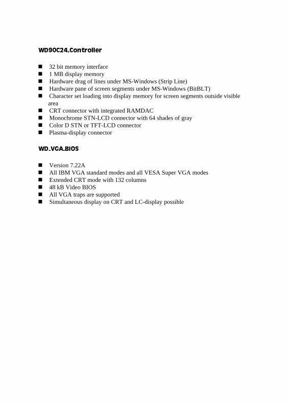
WD90C24-Controller
n 32 bit memory interfacen 1 MB display memoryn Hardware drag of lines under MS-Windows (Strip Line)n Hardware pane of screen segments under MS-Windows (BitBLT)n Character set loading into display memory for screen segments outside visible
arean CRT connector with integrated RAMDACn Monochrome STN-LCD connector with 64 shades of grayn Color D STN or TFT-LCD connectorn Plasma-display connector
WD-VGA-BIOS
n Version 7.22An All IBM VGA standard modes and all VESA Super VGA modesn Extended CRT mode with 132 columnsn 48 kB Video BIOSn All VGA traps are supportedn Simultaneous display on CRT and LC-display possible
11.1
1.2
1.3
22.12.1.12.1.22.1.32.1.42.22.2.12.2.22.2.32.2.42.2.52.2.62.2.72.2.82.32.3.12.42.4.1
33.1
3.23.2.13.2.2
1112
13
14
15151617181920232425262830313335364143
4545
464646
IntroductionProduct Introduction
Compatibility
Reference Documents
PCM-4330-InstallationHardware InstallationJumper JP1: Panel Off SignalJumper JP2: Contrast VoltageLC-Display Configuration SwitchesInstalling the PC/104-ModuleSetupTime and DataAT Hard DiskFloppy DiskBoot FeaturesStandard ChipsetTimeoutPeripheralsPeripherals(Advance)MS-DOS SVGA SoftwareDriver InstallationMS-Windows SVGA SoftwareDriver Installation
Layout and FunctionsBlock Circuit Diagram
General LayoutProcessor (CPU)Memory
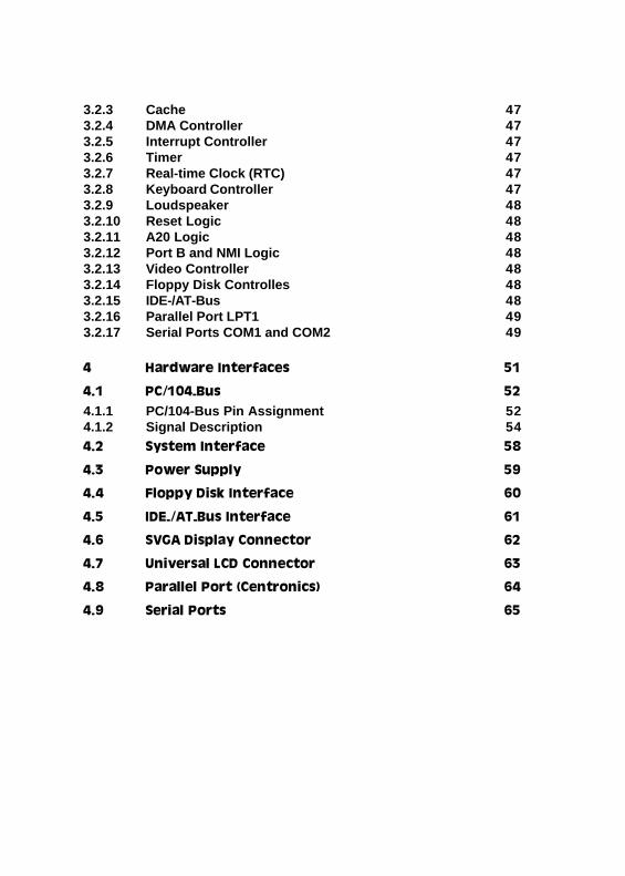
Table of Contents
474747474747484848484848484949
51
52525458
59
60
61
62
63
64
65
CacheDMA ControllerInterrupt ControllerTimerReal-time Clock (RTC)Keyboard ControllerLoudspeakerReset LogicA20 LogicPort B and NMI LogicVideo ControllerFloppy Disk ControllesIDE-/AT-BusParallel Port LPT1Serial Ports COM1 and COM2
Hardware Interfaces
PC/104-BusPC/104-Bus Pin AssignmentSignal DescriptionSystem Interface
Power Supply
Floppy Disk Interface
IDE-/AT-Bus Interface
SVGA Display Connector
Universal LCD Connector
Parallel Port (Centronics)
Serial Ports
3.2.33.2.43.2.53.2.63.2.73.2.83.2.93.2.103.2.113.2.123.2.133.2.143.2.153.2.163.2.17
4
4.14.1.14.1.24.2
4.3
4.4
4.5
4.6
4.7
4.8
4.9
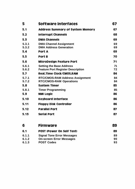
55.1
5.2
5.35.3.15.3.25.4
5.5
5.65.6.15.6.25.75.7.15.7.25.85.8.15.9
5.10
5.11
5.12
5.13
66.16.1.16.1.26.1.3
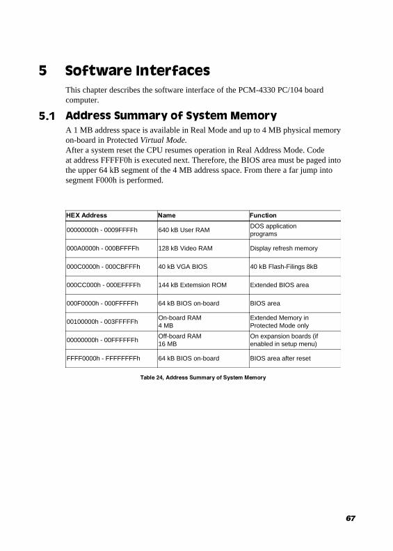
Software interfacesAddress Summary of System Memory
Interrupt Channels
DMA ChannelsDMA Channel AssignmentDMA Address GenerationPort A
Port B
MicroDesign Feature PortSetting the Base AddressFeature Port Register DescriptionReal-Time Clock/CMOS-RAMRTC/CMOS-RAM Address AssignmentRTC/CMOS-RAM OperationsSystem TimerTimer ProgrammingNMI Logic
Keyboard Interface
Floppy Disk Controller
Parallel Port
Serial Port
FirmwarePOST (Power On Self Test)Signal Tone Error MessagesOn-screen Error MessagesPOST Codes
6767
68
69696969
70
71 71
7284
84 84
85 85
86
86
86
87
87
8989899093

SVGA-BIOS Calls (INT 1Oh)Standard IBM VGA-compatible BIOS Calls (INT 1Oh)Extended BIOS Calls (INT 1Oh)VESA SuperVGA BIOS Calls (INT 1Oh)
Technical SpecificationsElectrical Specifications
Environment Conditions
Dimension Sketch
Appendix A: Troubleshooting
Appendix B: LC-Displays
Appendix C: Silicon Disk
Appendix D: Installing PC/104 Modules
6.26.2.16.2.26.2.3
77.1
7.2
7.3
9595
103106
109109
109
110
111
113
123
125

11
IntroductionThis manual describes the PCM-4330 PC/104 board computer with 486SX,486DX2, or 486DX4 CPU as a PC/104 module.
1
Figure 1, PCM-4330 with 486SX, 486DX2, or 486DX4-CPU (Top and Bottom View)
Several notes in the text refer to product documentation not included in this man-ual. If you need more comprehensive and detailed information, please refer to datasheets and documents listed under chapter 1.3.

12
Product IntroductionThe PCM-4330 serves as a processor board in a PC/104 environment and providesfor a fully ISA-compatible computer system. The system is built using the SIS-85C47i. This chip contains on a single VLSIcomponent the main elements of an ISA system by implementing DMA, memory,bus,interrupt controller, memory mapper, and timer. For addressing peripheral devices, a chip from Standard Microsystem Corpora-tion (SMC) is used on the board. The FDC37C92x-Ultra-I/O-Controller, built inSuperCelTM technology, includes IDE-/AT-bus, floppy disk, keyboard, serial, andparallel port controllers, as well as a real-time clock. The WD90C24 controller, addressing 1 MB of video memory via a 32 bit widedata bus, is used to control video output. The controller accelerates the screen dis-play of window systems like MS-Windows by hardware support of CPU intensivescreen operations. The graphics board supports all VGA, SVGA and Paradise en-hanced video modes.
DesignThe PCM-4330 board is AT-compatible including all interfaces. All software writ-ten for Intel 8086, 80286, 80386, 80486, and compatible processors runs on thisboard. It is built and fired in double-sided SMD technology requiring minimumspace for a maximum of functions.
ProcessorThe 486SX, 486DX2, and 486DX4 CPUs offer virtual addressing capabilities, inte-grated MMU, 4-level memory protection in multi-user-mode (Protected VirtualAddress Mode). 1 MB physical memory can be addressed in Real-Address-Modeand 4 GB in Protected Mode. Maximum virtual memory in Protected Mode is 64TB.
Co-processorAll DX-CPUs used for the PowerDwarf feature on-chip math co-processors.
CachePresently available CPUs from the i486 family include 8 kB 4-way-on-chip-cacheused for data and code caching by the CPU.
Main MemoryWith respect to the 486SX, 486DX2, and 486DX4 CPU capabilities, main memoryis addressed with an access width of 32 bit. RAM memory is parity checked. TwoDRAM modules with access times of 70 ns are used in sockets providing 1 MBwith/without parity (256K x 16 or 256K x 18), 4MB with/without parity (1M x16 or1M x 18), or 16MB (4M x 16) on-board system memory.
1.1

13
Silicon DiskThe PCM-4330 board can optionally be fitted with a 28F016SV (2MB) or 28F032SV(4 MB) flash module to provide a silicon disk, Data, programs, or operating soft-ware can be permanently stored on this disk. Data is accessed in16 kB banks that arepaged into the address space of the processor.128 kB from the available memoryspace of the flash module is used for the System-BIOS.
Video ControllerThe Western Digital WD90C24 video controller can address various monochromeor fiat panel displays directly, as well as all SVGA monitors. Depending on theLCD display connected, an additional CRT display may be used simultaneously.The WD90C24 offers accelerated display of windows via integrated hardware func-tions (such as Bit Block Transfer). Frame buffers and font-caching are also sup-ported.
Video MemoryThe 1 MB video memory on the VGA controller is addressed directly via a 32 bitwide interface from the video controller. The size of the video memory allows for aresolution of 1024 x 768 pixels (256 colors) on LED and CRT displays.
ROM-BIOSA 64 kB segment at address F000h is reserved for the Award ROM-B IO S. AllAT03-compatible traps are included in this address space. The Western Digital VGA-BIOS for the WD90C24 video controller uses 48 kBin the physical address space of the computer, starting at segment C000h. All VGA-, SVGA- and VESA-compatible video traps are supported by the BIOS. The memory area is fitted with a 29F010 (128 kB), 29F020 (256 kB), or 29F040(512 kB) Flash-Memory. Alternatively, the board can be equipped with a28F0xGSV(1 MB) or 28F032SV (4 MB) module to provide memory space for the BIOS and asilicon disk.
InterfacesThe PCM-4330 board includes the most important interfaces on-board. Two serialand one parallel port, keyboard, floppy disk and an IDE hard disk controller areincluded and can be configured by software. A SVGA connector is available, aswell as a connector for monochrome or color LC-display. The PCM-4330 singleboard computer features an expansion slot according to the PC/104 norm.
CompatibilityThe board is fully XT/AT-compatible. All available expansion cards complyingwith the PC/104 norm can be used with the PCM-4330.
1.2
14
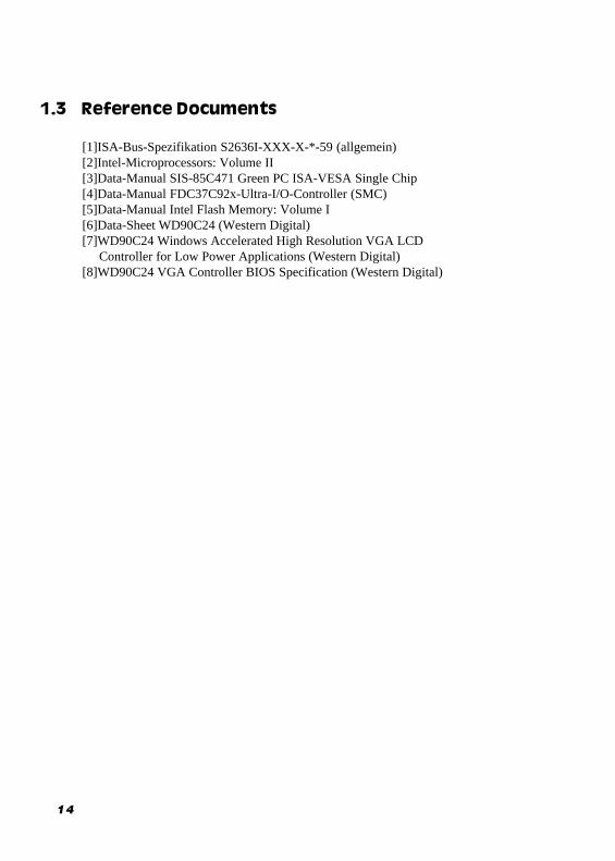
Reference Documents
[1]ISA-Bus-Spezifikation S2636I-XXX-X-*-59 (allgemein)[2]Intel-Microprocessors: Volume II[3]Data-Manual SIS-85C471 Green PC ISA-VESA Single Chip[4]Data-Manual FDC37C92x-Ultra-I/O-Controller (SMC)[5]Data-Manual Intel Flash Memory: Volume I[6]Data-Sheet WD90C24 (Western Digital)[7]WD90C24 Windows Accelerated High Resolution VGA LCD Controller for Low Power Applications (Western Digital)[8]WD90C24 VGA Controller BIOS Specification (Western Digital)
1.3
15
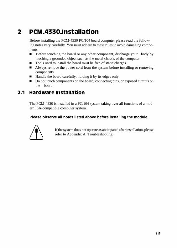
PCM-4330-InstallationBefore installing the PCM-4330 PC/104 board computer please read the follow-ing notes very carefully. You must adhere to these rules to avoid damaging compo-nents:n Before touching the board or any other component, discharge your body by
touching a grounded object such as the metal chassis of the computer.n Tools used to install the board must be free of static charges.n Always remove the power cord from the system before installing or removing
components.n Handle the board carefully, holding it by its edges only.n Do not touch components on the board, connecting pins, or exposed circuits on
the board.
Hardware Installation
The PCM-4330 is installed in a PC/104 system taking over all functions of a mod-ern ISA-compatible computer system.
Please observe all notes listed above before installing the module.
2
If the system does not operate as anticipated after installation, pleaserefer to Appendix A: Troubleshooting.
2.1
16
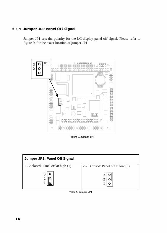
Jumper JPI: Panel Off Signal
Jumper JP1 sets the polarity for the LC-display panel off signal. Please refer tofigure 9. for the exact location of jumper JP1
321
JP1
Figure 2, Jumper JP1
321
321
1 - 2 closed: Panel off at high (1)
Jumper JP1: Panel Off Signal
2.1.1
2 - 3 Closed: Panel off at low (0)
Table 1, Jumper JP1
17
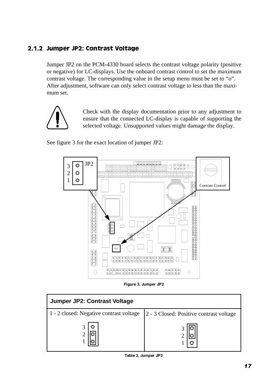
Jumper JP2: Contrast Voltage
Jumper JP2 on the PCM-4330 board selects the contrast voltage polarity (positiveor negative) for LC-displays. Use the onboard contrast control to set the maximumcontrast voltage. The corresponding value in the setup menu must be set to “o”.After adjustment, software can only select contrast voltage to less than the maxi-mum set.
2.1.2
Check with the display documentation prior to any adjustment toensure that the connected LC-display is capable of supporting theselected voltage. Unsupported values might damage the display.
See figure 3 for the exact location of jumper JP2:
321
JP2
321
321
1 - 2 closed: Negative contrast voltage
Jumper JP2: Contrast Voltage
2 - 3 Closed: Positive contrast voltage
Figure 3, Jumper JP2
Contrast Control
Table 2, Jumper JP2
18
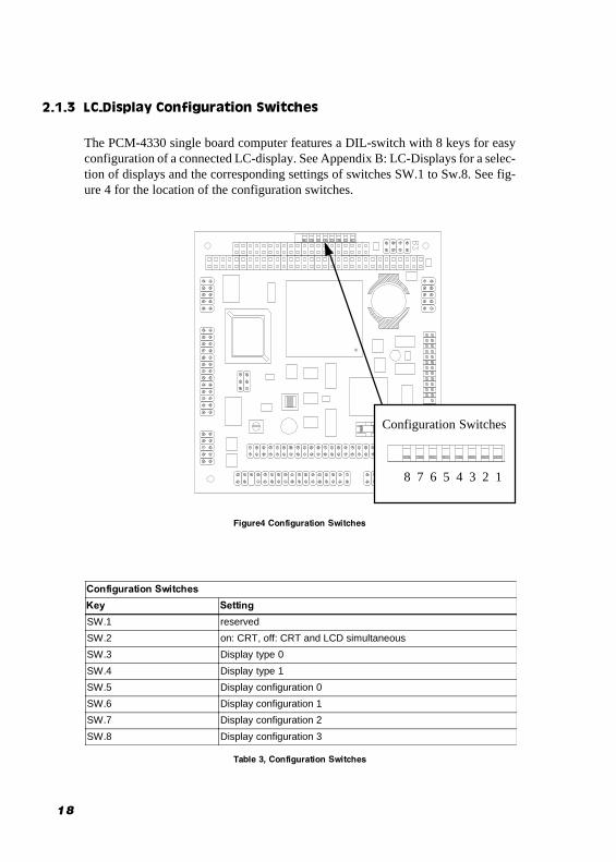
LC-Display Configuration Switches
The PCM-4330 single board computer features a DIL-switch with 8 keys for easyconfiguration of a connected LC-display. See Appendix B: LC-Displays for a selec-tion of displays and the corresponding settings of switches SW.1 to Sw.8. See fig-ure 4 for the location of the configuration switches.
2.1.3
8 7 6 5 4 3 2 1
Configuration Switches
Configuration Switches
Key Setting
SW.1 reserved
SW.2 on: CRT, off: CRT and LCD simultaneous
SW.3 Display type 0
SW.4 Display type 1
SW.5 Display configuration 0
SW.6 Display configuration 1
SW.7 Display configuration 2
SW.8 Display configuration 3
Table 3, Configuration Switches
Figure4 Configuration Switches
19
Installing the PC/104-ModuleThe PCM-4330 is installed in a PC/104 system and takes over the function of theCPU. Please observe the following guidelines for the installation of the module:
2.1.4
8 Switch off the computer system.8 Remove the power cord.8 Remove the cover or housing of the computer system8 If a PC/104-CPU-board, VGA graphics adapter, IDE-hard disk or floppy disk
controller is installed in the system, remove it. The PCM-4330 comprises allfunctions of these boards.
8 Carefully install the PCM-4330 in the PC/104 system. The board features fourholes for safe fastening and a connector for the installation on a PC/ 104 bus.
8 Connect all cables and connectors with the appropriate interfaces (system,LPT1,COM1, COM2, VGA/LCD, IDE hard disk, floppy disk, and power). See chap-ter 4.
8 Replace the housing cover and plug in the power cord.8 Switch on the computer system.8 Call the Setup-Menu.
Check that jumpers Jp1 and Jp2 and all configuration switches areset correctly before installation.
20
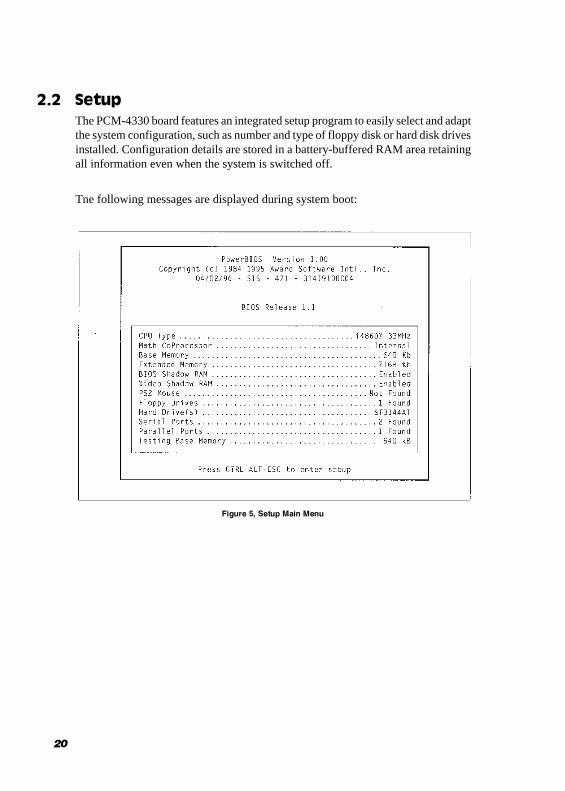
2.2
Figure 5, Setup Main Menu
SetupThe PCM-4330 board features an integrated setup program to easily select and adaptthe system configuration, such as number and type of floppy disk or hard disk drivesinstalled. Configuration details are stored in a battery-buffered RAM area retainingall information even when the system is switched off.
Tne following messages are displayed during system boot:

21
The following selections are available in the setup menu:
User HelpThis selection displays a screen with help message and instructions on how to uselist boxes and radio buttons.
Load DefaultsUse this option to reset current settings to factory default values.
Time and DateUse this selection to set time and date.
AT Hard DiskThis selection offers automatic detection and manual drive parameter configurationof IDE-/AT-Bus hard disk drives connected to the primary (on-board) and second-ary IDE-Controller. If using the BIOS automatic detection, several drive types maybe available. Extended modes for IDE hard disk with a capacity of more than 528MB are supported by the BIOS.
Floppy DiskSelect type of floppy disk drives installed.
After pressing the CTRL-ALT-ESC keys, the following menu is displayed:
Figure 6, Setup Menu

22
Boot FeaturesAdditional configuration features for system boot.
Standard ChipsetSettings for Cache and Shadow.
TimeoutSelect to switch off screen or spin down IDE hard disk drives after specified time ofinactivity.
PeripheralsSetup settings for serial ports, parallel port, IDE-/AT-Bus-Controller, Floppy DiskController and PS/2-Mouse.
Peripherals Adv.Sehup settings for feature controller, silicon disk and LC display.
System StatusInformation on temperature and voltage (read only).
Use the arrow keys to navigate between menu selections and press RETURN toenter the chosen dialog box. Use the TAB keys to jump between list boxes andbuttons. To return to the setup menu or leave the setup program, hit ESC (or press theEXIT or CANCEL button). Before leaving the setup program, a confirmation box appears. Press SAVE tosave all settings and leave the setup program, press EXIT the button or hit the ESCkey to discard all changes and leave the setup program without saving, or pressRETURN to return to the setup menu:

23
Time and DateAfter selecting Time and Date the following dialog box appears:
2.2.1
The following parameters can be set (Use the TAB keys to jump between selec-tions):
DateEnter the current date in the form tt-MM-JJJJ
TimeEnter current system time in the format hh:mm:ss
Figure 7, Date and Time Setup

24
AT Hard DiskAfter selecting AT Hard Disk the following dialog box is displayed:
2.2.2
Figure 8, �AT Herd Disk� Setup
Use the arrow keys to navigate to the appropriate hard disk drives settings or jumpbetween buttons using the TAB keys. Press the AUTO All Drives button to config-ured drive parameters automatically or enter the applicable values. Use the AUTOcheckmark to automatically detect the drive type during system boot and set theappropriate period of time the system is to wait for the drive to spin up (drive waittime).
25
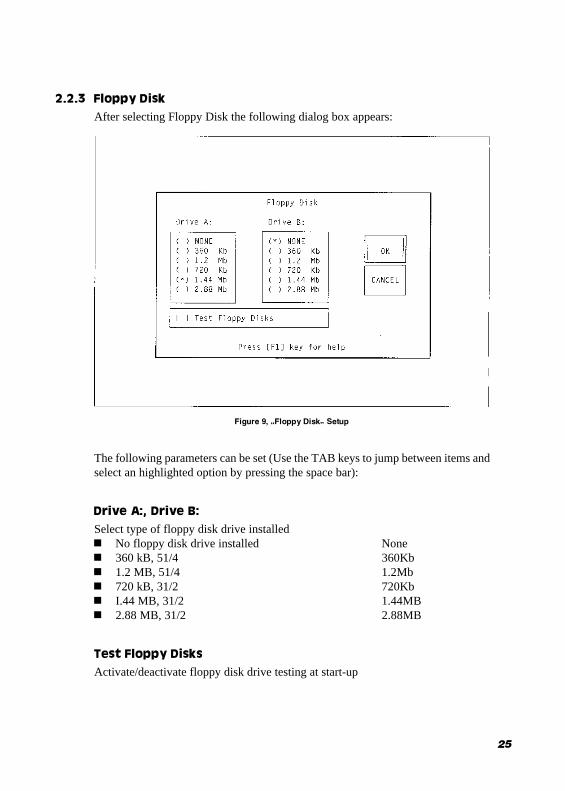
Floppy DiskAfter selecting Floppy Disk the following dialog box appears:
Figure 9, �Floppy Disk� Setup
The following parameters can be set (Use the TAB keys to jump between items andselect an highlighted option by pressing the space bar):
Drive A:, Drive B:Select type of floppy disk drive installedn No floppy disk drive installed Nonen 360 kB, 51/4 360Kbn 1.2 MB, 51/4 1.2Mbn 720 kB, 31/2 720Kbn I.44 MB, 31/2 1.44MBn 2.88 MB, 31/2 2.88MB
Test Floppy DisksActivate/deactivate floppy disk drive testing at start-up
2.2.3
26
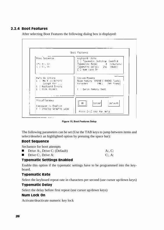
Boot FeaturesAfter selecting Boot Features the following dialog box is displayed:
Figure 10, Boot Features Setup
The following parameters can be set (Use the TAB keys to jump between items andselect/deselect an highlighted option by pressing the space bar):
Boot SequenceSecluence for boot attemptsn Drive A:, Drive C: (Default) A:, C:n Drive C:, Drive A: C:, A:
Typematic Settings EnabledEnable this option if the typematic settings have to be programmed into the key-board.
Typematic RateSelect the keyboard repeat rate in characters per second (use cursor up/down keys)
Typematic DelaySelect the delay before first repeat (use cursor up/down keys)
Num Lock OnActivate/deactivate numeric key lock
2.2.4
27
Halt On ErrorsHalt boot on errors. Select which errors not to halt boot on:
n Keyboard errorn Disk errors
Base MemoryBase memory size
Extended MemoryExtended memory size
Quick Memory TestActivate/deactivate quick memory testing
Language IsSelect language for POST and error messages (see also Figure 5 on page 16). Usethe arrow up and down keys to navigate to select a desired language.n English boot messages (Default) Englishn German boot messages Germann French boot messages French
Display Graphic LogoActivate/deactivate graphic logo display during system boot

28
Standard ChipsetAfter selecting Standard Chipset the following dialog box appears:
Figure 11,�Standard Chipset� Setup
The following parameters can be set (Use the TAB keys to jump between items andselect/deselect an highlighted option by pressing the space bar):
CacheActivate/Deactivate system cache. If an external cache is not available, this optioncan not be selected.n Cache off Disablen CPU cache only CPU onlyn Cache on CPU and External
Cache Write BackSelect writeback cache fiunction for CPU cache. This option can only be selected ifsupported by the CPU installed.
External Cache Write BackSelect writeback cache function for external (level z) cache. This option can only beselected if second level cache is installed on the board.
2.2.5

29
Boot SpeedDefine bootup system speedn Full operation speed Highn Reduced CPU speed for bootup Low
Onboard ParityEnable onboard parity checking if parity RAM is installed
Enable Flash UpdateEnable System-ROM update (i.e. disable flash module write protection). After check-ing this option, the System-ROM Flash module will be unprotected at next poweron and automatically be cleared again at the following power on. If option is notchecked, the System-ROM is write protected.
ShadowActivate/deactivate shadowing for memory area
30
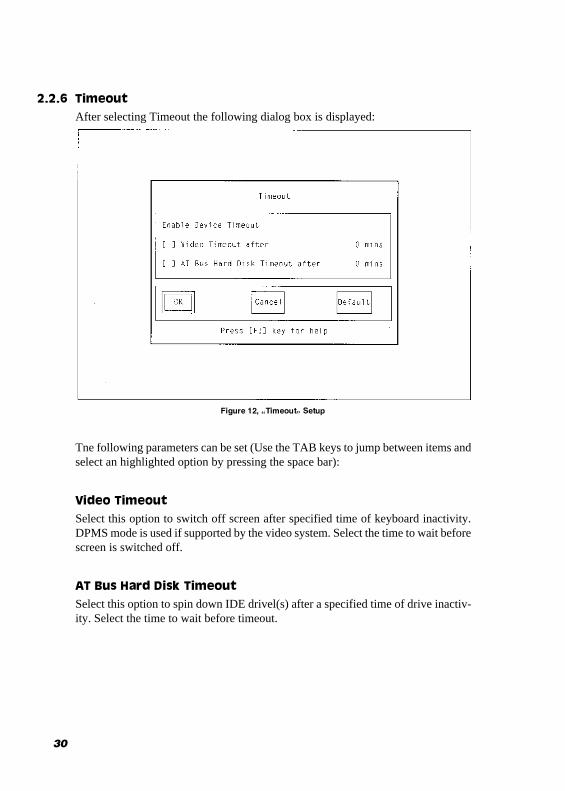
TimeoutAfter selecting Timeout the following dialog box is displayed:
Figure 12, �Timeout� Setup
Tne following parameters can be set (Use the TAB keys to jump between items andselect an highlighted option by pressing the space bar):
Video TimeoutSelect this option to switch off screen after specified time of keyboard inactivity.DPMS mode is used if supported by the video system. Select the time to wait beforescreen is switched off.
AT Bus Hard Disk TimeoutSelect this option to spin down IDE drivel(s) after a specified time of drive inactiv-ity. Select the time to wait before timeout.
2.2.6

31
PeripheralsAfter selecting Peripherals the following dialog box appears:
Figure 13, Peripherals Setup
The following parameters can be set (Use the TAB keys to jump between items andselect/deselect an highlighted option by pressing the space bar):
Serial Port ASelect base address for serial port In Automatic assignment at start-up Auton Select address and interrupt 3F8h, IRQ4.
2F8h, IRQ33E8h, IRQ42E8h, IRQ3
n Not active Disable
Serial Port BSelect base address for serial port 2n Automatic assignment at start-up Auton Select address and interrupt 3F8h, IRQ4
2F8h, IRQ33E8h, IRQ42E8h, IRQ3
n Not active Disable
2.2.7
32
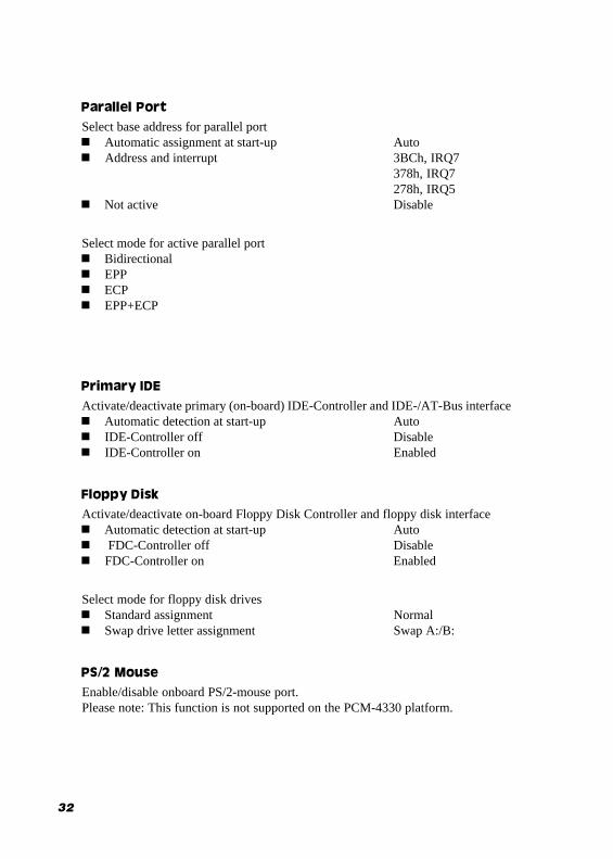
Parallel PortSelect base address for parallel portn Automatic assignment at start-up Auton Address and interrupt 3BCh, IRQ7
378h, IRQ7278h, IRQ5
n Not active Disable
Select mode for active parallel portn Bidirectionaln EPPn ECPn EPP+ECP
Primary IDEActivate/deactivate primary (on-board) IDE-Controller and IDE-/AT-Bus interfacen Automatic detection at start-up Auton IDE-Controller off Disablen IDE-Controller on Enabled
Floppy DiskActivate/deactivate on-board Floppy Disk Controller and floppy disk interfacen Automatic detection at start-up Auton FDC-Controller off Disablen FDC-Controller on Enabled
Select mode for floppy disk drivesn Standard assignment Normaln Swap drive letter assignment Swap A:/B:
PS/2 MouseEnable/disable onboard PS/2-mouse port.Please note: This function is not supported on the PCM-4330 platform.
33
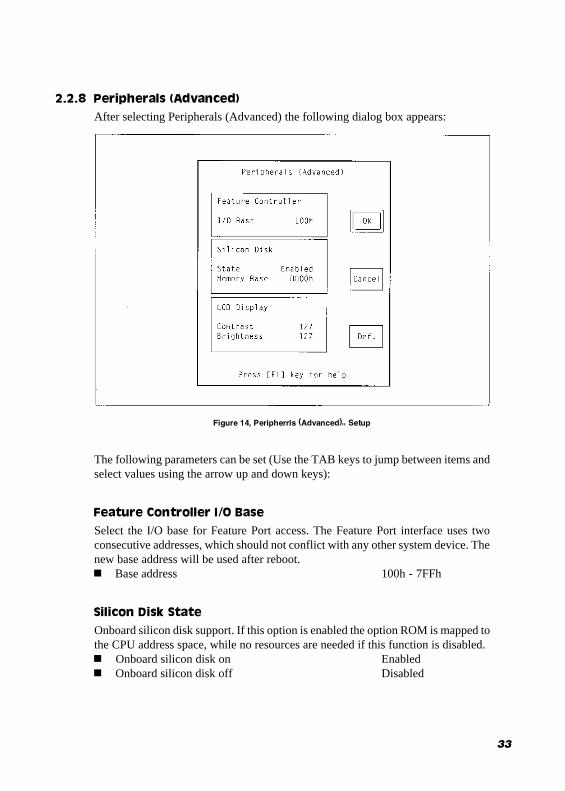
Peripherals (Advanced)After selecting Peripherals (Advanced) the following dialog box appears:
Figure 14, Peripherrls (Advanced)� Setup
The following parameters can be set (Use the TAB keys to jump between items andselect values using the arrow up and down keys):
Feature Controller I/O BaseSelect the I/O base for Feature Port access. The Feature Port interface uses twoconsecutive addresses, which should not conflict with any other system device. Thenew base address will be used after reboot.n Base address 100h - 7FFh
Silicon Disk StateOnboard silicon disk support. If this option is enabled the option ROM is mapped tothe CPU address space, while no resources are needed if this function is disabled.n Onboard silicon disk on Enabledn Onboard silicon disk off Disabled
2.2.8
34
Silicon Disk Memory BaseDefine the 16 kB memory window within the CPU address space to be used forsilicon disk access.n Memory Base D000h/D400h/D800h/
DC00h/CC00h
LCD Display ContrastSelect LC display bootup value for contrast. As visual feedback, the new value willbe programmed immediately.n Contrast value 0 - 255
LCD Display BrightnessSelect LC display boohup value for brightness. As visual feedback, the new valuewill be programmed immediately.n Brightness value 0 - 255

35
MS-DOS SVGA Software
Special SVGA software (drivers and programs) is included with the PCM-4330single board computer to use the extended functions under MS-DOS. Operation ofthe SVGA adapter is also possible without this SVGA software.
The SVGA software for use with MS-DOS is found on the disk labeled DOS InstallDisk. The following files are included on this disk:
Textn README.TXT Lists all drivers and programs on the diskn README.1ST (If included on the disk) Contains last-minute informa-
tion and change remarks
Driversn ACAD.LIF AutoCAD 386, AutoShade and 3D Studio display drivern CADVANCE.LIF Cadvance display drivern GENERIC.LIF Generic CADD display drivern LOTUS.LIF Lotus 1-2-3 and Lotus Symphony display drivern PCAD.LIF PCAD display drivern WORD.LIF Microsoft Word for MS-DOS display drivern WP.LIF WordPerfect display drivern UTILITY. LIF ANSI.SYS driver for extended VGA mode (Paradise
Mode)
Programsn INSTALL. COM Menu controlled installation programn CHIPTST. EXE (used by INSTALL.COM)n KDINSTAL. EXE (used by INSTALL.COM)n READID.EXE (used by INSTALL.COM)n VGAMODE.EXE (used by INSTALL.COM)
2.3
If the system does not operate as anticipated after the installationof a MS-DOS device driver, please refer to AppendixA:Troubleshooting.

36
Driver Installation
To use the extended features of the WD90C24 controller under MS-DOS specialSVGA software (programs and drivers) must be installed. The disk DOS-InstallDisk contains the menu-controlled program INSTALL.COM.8 Make a backup copy of the disk DOS-Install Disk and store the original at a
secure place.8 Check whether the PCM-4330 single board computer is correctly installed in
the system and that all jumpers and switches are set properly.8 Load the utility program INSTALL.COM from your backup copy of the in-
stallation disk from dis
The following start-up page of the installation utility appears on the screen. It con-tains the version number and copyright information:
2.3.1
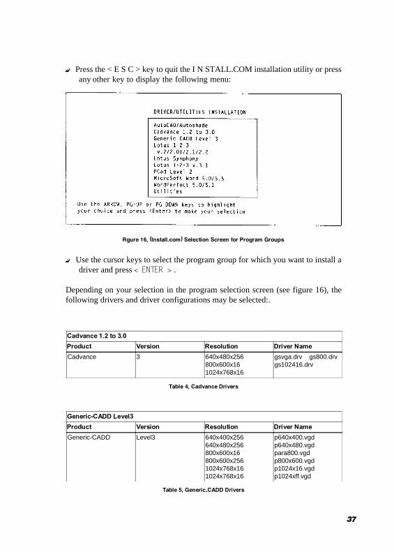
Figure 15, (Install.com) Start-up Screen
37
Rgure 16, (Install.com) Selection Screen for Program Groups
8 Use the cursor keys to select the program group for which you want to install adriver and press < ENTER > .
Depending on your selection in the program selection screen (see figure 16), thefollowing drivers and driver configurations may be selected:.
Table 5, Generic-CADD Drivers
Generic-CADD Level3
Product Version Resolution Driver Name
Generic-CADD Level3 640x400x256640x480x256800x600x16800x600x2561024x768x161024x768x16
p640x400.vgdp640x480.vgdpara800.vgdp800x600.vgdp1024x16.vgdp1024xff.vgd
Table 4, Cadvance Drivers
Cadvance 1.2 to 3.0
Product Version Resolution Driver Name
Cadvance 3 640x480x256800x600x161024x768x16
gsvga.drv gs800.drvgs102416.drv
8 Press the < E S C > key to quit the I N STALL.COM installation utility or pressany other key to display the following menu:
38
Lotus 1-2-3 v.2/2.01/2.1/2.2
Product Version Resolution Driver Name
Lotus 1-2-3 2,2.1,2.01,2.2 640x480x16800x600x161024x768x16123Columns
sp1_480s.drvsp1_600s.drvsib2vga.drv(8x9font)sib3vga.drv(9x13font)s0_25s.drv(132x25)sp0_44s.drv(132x44)
Lotus Symphony
Product Version Resolution Driver Name
Lotus Symphony 1.1,1.2,2.0 640x480x16800x600x161024x768x16123Columns
sp1_480s.drvsp1_600s.drvsib2vga.drv(8x9font)sib3vga.drv(9x13font)s0_25s.drv(132x25)sp0_44s.drv(132x44)
Table 6, Lotus 1-2-3 Drives
Table 7, Lotus Symphony Drives
Lotus 1-2-3 v.3.1
Product Version Resolution Driver Name
Lotus 1-2-3 3.1 800x600x161024x768x16
l13v600.dldl13v768.dld
Table 8, Lotus 1-2-3 v.3.1 Drivers
PCad Level2
Product Version Resolution Driver Name
PCAD Level2 800x600x161024x768x16
dwdpvga.drvdpvga1k.drv
Table 9, PCad Drivers
Microsoft Word 5.0/5.5
Product Version Resolution Driver Name
WORD v5.5 800x600x16 vga.gsd
Table 10, Microsoft Word 5.0/5.5 Drivers

39
WordPerfect 5.0/5.1
Product Version Resolution Driver Name
WordPerfect v5.0 800x600x161024x768x16
wdpvga1.wpdwdpvga2.wpd
WordPerfect v5.1 1024x768x16 wdpvga3.vrs
Table 11, WordPerfect 5.0/5.1 Drivers
AutoCAD/Autoshade
Product Version Resolution Driver Name
AutoCAD 386Non D.L.Auto Shade 3863D Studio
Release 11Version 2
640x480x256640x480x256 / 32k640x480x256 / 32k
11p6168.exp11p6168.exp11p6168.exp
AutoCAD 386Non D.L.Auto Shade 3863D Studio
Release 11Version 2
800x600x256 / 32k800x600x256 / 32k800x600x256 / 32k
11p8188.exp11p8188.exp11p8188.exp
AutoCAD 386Non D.L.Auto Shade 386
Release 11Version 2
640x480x256640x480x256
11pshv68.exp11pshv68.exp
AutoCAD 386Non D.L.Auto Shade 386
Release 11Version 2
800x600x256800x600x256
11pshv88.exp11pshv88.exp
AutoCAD 386Non D.L.Auto Shade 386
Release 11Version 2
1024x768x2561024x768x256
11pshv18.exp11pshv18.exp
AutoCAD 386 Release 11 800x600x16800x600x2561024x768x161024x768x256
11pdlv84.exp11pdlv88.exp11pdlv14.exp11pdlv18.exp
Auto Shade Version 1 640x400x256640x480x256800x600x2561024x768x256
rd400.exerd480.exerd800.exerd1024.exe
Table 12, AutoCAD Drivers
Utilities
Driver Description
WDANSI.SYS ANSI.SYS driver for extended VGA mode
Table 13, #Utilities

40
8 After selecting a driver and display resolution, the installation utility requeststhe target drive and the name of the destination directory to receive the driversoftware.The following example installs the driver into the directory that contains theLotus1-2-3 software.
8 Use the cursor keys to select a drive letter from the list of avafiable drives andpress <ENTER>.
8 Please read all instructions carefully as the actual input parameters may varyaccording to the driver selected.
8 Enter the subdirectory and press <ENTER>.
Select the Drive on which to install Lotus Driver
Drive A:Drive B:Drive C:Drive D:Drive E:
Which subdirectory is Lotus installed ?
Figure 17, (Install.com)Destination Drive
Figure 18,(Install.com)Destination Subdirectory
41
MS-Windows SVGA SoftwareSpecial SVGA software (programs and drivers) is included with the PCM-4330 touse extended functions of the video controller under MS-Windows. Operation ofthe SVGA adapter is also possible without this special SVGA software.
The SVGA software for use with MS-Windows is found on the disk labeledWindolvs-Install-Disk. The following files are found on this disk:
Driversn vga .dr_ Windows 3.1 driver(standard VGA)n wd24_8 .dr_ Windows 3.1 drivern wd24ik_4.dr_ Windows 3.1 drivern wd2464__4.dr_ Windows 3.1 drivern wd2464_h.dr_ Windows 3.1 drivern wd2480_4.dr_ Windows 3.1 drivern wddci.dr_ Windows 3.1 driver
Character Setsn 8514fix.fo_ Windows 3.1 character setn 8514oem.fo_ Windows 3.1 character setn 85x4sys.fo_ Windows 3.1 character setn cga4owoa.fo_ Windows 3.1 character setn cga8owoa.fo_ Windows 3.1 character setn coure.fo_ Windows 3.1 character setn courf. fo_ Windows 3.1 character setn dosapp.fo_ Windows 3.1 character setn ega4owoa.fo_ Windows 3.1 character setn ega8owoa.fo_ Windows 3.1 character setn serife.fo_ Windows 3.1 character setn seriff. fo_ Windows 3.1 character setn smalle.fo_ Windows 3.1 character setn smallf. fo_ Windows 3.1 character setn sserife.fo_ Windows 3.1 character setn sseriff. fo_ Windows 3.1 character setn symbole.fo_ Windows 3.1 character setn symbolf. fo_ Windows 3.1 character set
2.4

42
vgaoem.fo_ Windows 3 .1 character setvgasys .fo_ Windows 3 .1 character setvgafix.fo_ Windows 3 .1 character set
SetupProgramssetup.exe Windows 3 .1 setup filesetup.inf Windows 3 .1 setup filesetup.lst Windows 3 .1 setup filesetup.rest Windows 3 .1 setup filesetupapi.inc Windows 3 .1 setup filedciman.dl_ Windows 3 .1 setup filemscomstf. dll Windows 3 .1 setup filemscuisff. dll Windows 3 .1 setup filemsdetsff. dll Windows 3 .1 setup filemsinssff. dll Windows 3 .1 setup filemsshlstf. dll Windows 3 .1 setup filemsuilsff. dll Windows 3 .1 setup fileoemsetup.inf Windows 3 .1 setup filepvga.gr_ Windows 3 .1 setup filev7vga.3g Windows 3 .1 setup filevddpvga.38- Windows 3 .1 setup filever.dll Windows 3 .1 setup filevgalogo.lg_ Windows 3 .1 setup filevgalogo .fi_ Windows 3 .1 setup filevidchg.ex_ Windows 3 .1 setup filevidchg.hl_ Windows 3 .1 setup file_mssetup.exe Windows 3 .1 setup file_mstest.exe Windows 3 .1 setup file
If the system does not operate as anticipated after the installation ofa MS-Windows device driver, please refer to Appendix A: Trouble-shooting.
43
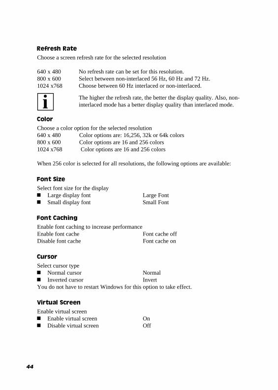
ResolutionSelect a resolution for the video driver640 x 480 This resolution supports the following color settings: 16,25,32k
and 64k colors
800 x 600 This resolution supports 16 and 256 colors. The screen refresh ratemay also be set: 56 Hz, 60 Hz and 72 Hz, non-interlaced, are supported.
1024 x 768 This resolution also supports 16 or 256 colors. Screen refresh ratecan be set to 60 Hz interlaced or non-interlaced.
Driver InstallationTo use extended features of the SVGA controllers on the PCM-4330 single boardcomputer under MS-Windows special SVGA drivers must be installed. The Windows-Install-Disk contains a special installation program to installSVGA video drivers and change video settings under MS-Windows. Use the MS-Windows File Manager or Program Manager to start the installation. On-line-Helpis available at every stage.
2.4.1
Please check with your monitor specifications to ensure that the mon-itor is capable of supporting the particular option, to prevent dam-age to the display.
Figure 19, Western Digital Video Changer
44
ColorChoose a color option for the selected resolution640 x 480 Color options are: 16,256, 32k or 64k colors800 x 600 Color options are 16 and 256 colors1024 x768 Color options are 16 and 256 colors
When 256 color is selected for all resolutions, the following options are available:
Font SizeSelect font size for the displayn Large display font Large Fontn Small display font Small Font
Font CachingEnable font caching to increase performanceEnable font cache Font cache offDisable font cache Font cache on
CursorSelect cursor typen Normal cursor Normaln Inverted cursor InvertYou do not have to restart Windows for this option to take effect.
Virtual ScreenEnable virtual screenn Enable virtual screen Onn Disable virtual screen Off
Refresh RateChoose a screen refresh rate for the selected resolution
640 x 480800 x 6001024 x768
No refresh rate can be set for this resolution.Select between non-interlaced 56 Hz, 60 Hz and 72 Hz.Choose between 60 Hz interlaced or non-interlaced.
The higher the refresh rate, the better the display quality. Also, non-interlaced mode has a better display quality than interlaced mode.i
45
Layout and FunctionsThis chapter describes the technical layout and functions of the PCM-4330 singleboard computer.
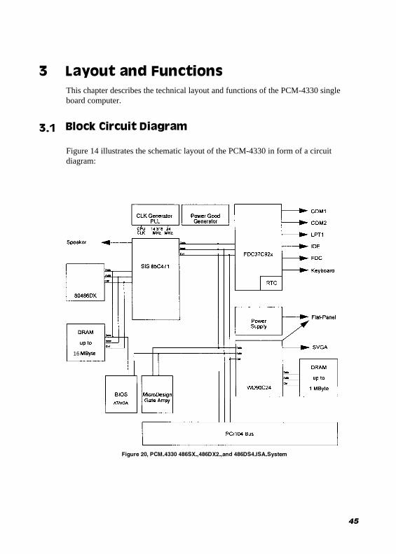
Block Circuit Diagram
Figure 14 illustrates the schematic layout of the PCM-4330 in form of a circuitdiagram:
Figure 20, PCM-4330 486SX-,486DX2-,and 486DS4-ISA-System
3
3.1
16
46
General LayoutThe following sections describe the individual components of the PCM-4330 sin-gle board computer.
Processor (CPU)A 32-bit CPU from the Intel i486 family is used. The PCM-4330 may be fittedwith a 486SX, 486DX2, or 486DX4 processor.
All these processors feature:Separate address and data busExtensive instruction set, downward compatible to the 8086 setIntegrated memory management (MM U)Memory protection on 4 levelsAddress space of 1 MB in Real ModePhysical addressable address space of up to 4 GB in Protected Mode
The processor can be operated in Real Address Mode or Protected Virtual Mode.After a reset, the processor resumes operation in Real Mode.
MemoryMemory on the PCM-4330 consists of ROM and RAM area depending on theboard configuration, ROM memory size is 128 kB to 4 MB. 128 kB are locatedbelow the 1 MB and 4 GB address boundary. It is therefore available twice (mir-rored). A socket is used for ROM memory modules with a 8-bit word width con-taining a 29F010 (128 kB), 29F020 (256 kB), or 29F040 (512 kB) Flash-Memory.Alternatively, a 28F016SV (I MB) or 28F032SV (4 MB) module can be used, whichalso offers silicon disk capabilities. The BIOS software can be reprogrammed by anauxiliary program during operation.
RAM is build up by two dynamic memory modules in sockets to offer 1 MB, 4MBor 16 MB on-board. These RAM modules support an access width of 32 bit and maybe parity checked bitwise (optional).
Specific attributes can be assignedto certain regions of RAM memory:n Enable/Disable Shadown RAM
3.2
3.2.1
Table 14, RAM Area Attributes
3.2.2
16MB
1024kBBIOS128kB
enable/disableRAM
896kBCHANNEL-I/O128kB
enable/DisableRAM
768kBVideo-Buffer128kB
enable/disableRAM
640kB DOS-area
47
Accessing the silicon disk is performed via 16 kB banks, that are paged into theaddress space of the processor. I/O port may be assigned for paging and individualbanks may be designated for paging. Read operations can be performed on bytes,words or double-words. Special software must be used to write to the silicon disk,removing the write protection before write operations.
CacheThe i486 family of processors all feature 8 kB on-chip cache and cache controller.
DMA ControllerThe DMA controller of the SIS-85C471-AT-Controller offers the ISA functionalityof two 82C37-DMA controllers with seven independent channels.
Interrupt ControllerTwo 82C59-compatible interrupt controllers are implemented. They are cascadedand offer 2 external interrupt channels.
TimerA 82C54-compatible timer is also included. It comprises three independent chan-nels which can be programmed in six different modes.
Real-time Clock (RTC)The RTC is included in the MC146818A-compatible cell of the FDC37C92x-Ultra-I/O-Controller. It is extended by 128 bytes via two 64 byte CMOS RAM pages inaddress space 40h - 7Fh of the RTC. The RTC manages system time, date, and offers alarm functions. 14 of 192bytes of internal memory are used to control the clock functions, the remaining 178bytes of CMOS RAM are used to store BIOS setup information.
Keyboard ControllerThe keyboard interface is implemented as a megacell in the SMC FDC37C92x-Ultra-I/O-Controller. In addition to the serial keyboard port, two ports for systemstatus and control functions are available.The keyboard controller manages:n Keyboard lockn Color/monochrome togglingn Address line A20 (1 MB limit)n Keyboard resetn Keyboard interrupt request IRQ1
3.2.3
3.2.4
3.2.5
3.2.6
3.2.7
3.2.8
48
LoudspeakerThe tone signal for the speaker is generated by Timer 2 (in the SIS-85C471-AT-Controller). The timer is programmed as a square-wave generator. The generator iscontrolled by the System-Control-Registers in Port B. An additional bit of the Sys-tem-Control-Registers is combined with output of Timer 2 by a logical and.Theresulting signal controls the internal or external speaker (using the system inter-face; c.f. Figure 23 on page 54).
Reset LogicA system reset may be initiated by the power supply, shutdown, keyboard reset orvia I/O port 92h (Bit 0) and the SIS-85C471-AT-Controller.
A20 LogicThe CPU line mask-A20 can be controlled as in AT-systems through the key-boardcontroller. Additionally, the PS/2®-compatible port 92h (Bit 1) is available.
Port B and NMI LogicThe status and control port B (061h) consists of the integrated System-Control-Register and the System-Status-Buffer. Parity checking may be enabled/disabledvia the System-Control-Register. The System-Status-Buffer informs on queuedmemory parity errors.
Video ControllerThe Western Digital WD90C24 video controller can address various monochromeor color flat panel displays directly, as well as regular SVGA monitors. A 2-row 10-pin connector for SVGA displays and a 2-row 40-pin universal LCD-onnectorarelocated on the board.
Floppy Disk ControllerThe FDC37C92x-Ultra-I/O-Controller from SMC with a licensed 765B-compatibleSuperCellTM is used for floppy disk control. Data is exchanged over DMA channel2,interrupts are initiated via IRQ6. Up to two floppy disk drives (31/2 or 51/4) are sup-ported.
IDE-/AT-BusThe FDC37C92x peripheral unit also includes an interface for IDE-/AT-bus harddisks.
3.2.10
3.2.9
3.2.11
3.2.12
3.2.13
3.2.14
3.2.15

49
Parallel Port LPT1The parallel port LPT1 is also integrated into the FDC37C92x-Ultra-I/O-ontroller.In addition to the PC/AT standard it can be operated in bi- as wall as in uni-direc-tional mode. This interface is equipped with a ChiProtectTM circuit protecting itfrom power surges at power-on of the printer device. I/O addresses are selectablein the setup menu. LPT1 is a 26-pin 2-row male connector on the board and can beextended to the exterior with an extension cable.
Serial Ports COM1 and COM2Interfaces COM1 and COM2 are included in the FDC37C92x-Ultra-I/O-ontrolleras a NS16550-compatible SuperCelLTM. I/O addresses are selectable in the set-upmenu; interrupts (IRQn) are pre-assigned and can not be selected by the user. COM1and COM2 are located as 2-row 10-pin connectors on the PCM-4330 single boardcomputer.
3.2.16
3.2.17

50

51
SVGA
Universal-LCD
IDE-/AT-Bus
System Interface
Power Supply
Hardware InterfacesAll interfaces required for an AT-compatible PC are included on-board. Figure 21illustrates the location of interfaces and connectors on the PCM-4330 PC/104 singleboard computer.
The following sections describe individual interfaces of the PCM-4330 in detail.
Figure 21, Location of on-board Interfaces
4
PC/104-Bus
PC/104-Bus
COM1
LPT1
COM2

52
SM C ®
PC/104-BusThe PC/104-Bus is a multimaster bus featuring:n 24-bit addressing for CPU, DMA and busmastern 8-bit or 16-bit datan Multimaster capabilityn 11 interrupt channels, flank triggeredn 7 DMA channels (four 8-bit, three 16-bit)n Waitstate controln Refresh control
PC/104-Bus Pin Assignment
The PCM-4330 features a PC/104-Bus. Please refer to table 16 for the pin assign-ment on the PC/104-Bus.
Figure 22, PC/104-Bus
D0C0
A1B1
PC/104-Bus
53
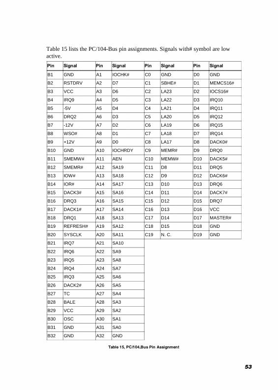
Table 15 lists the PC/104-Bus pin assignments. Signals with# symbol are lowactive.
Table 15, PC/104-Bus Pin Assignment
Pin Signal Pin Signal Pin Signal Pin Signal
B1 GND A1 IOCHK# C0 GND D0 GND
B2 RSTDRV A2 D7 C1 SBHE# D1 MEMCS16#
B3 VCC A3 D6 C2 LA23 D2 IOCS16#
B4 IRQ9 A4 D5 C3 LA22 D3 IRQ10
B5 -5V A5 D4 C4 LA21 D4 IRQ11
B6 DRQ2 A6 D3 C5 LA20 D5 IRQ12
B7 -12V A7 D2 C6 LA19 D6 IRQ15
B8 WSO# A8 D1 C7 LA18 D7 IRQ14
B9 +12V A9 D0 C8 LA17 D8 DACK0#
B10 GND A10 IOCHRDY C9 MEMR# D9 DRQ0
B11 SMEMW# A11 AEN C10 MEMW# D10 DACK5#
B12 SMEMR# A12 SA19 C11 D8 D11 DRQ5
B13 IOW# A13 SA18 C12 D9 D12 DACK6#
B14 IOR# A14 SA17 C13 D10 D13 DRQ6
B15 DACK3# A15 SA16 C14 D11 D14 DACK7#
B16 DRQ3 A16 SA15 C15 D12 D15 DRQ7
B17 DACK1# A17 SA14 C16 D13 D16 VCC
B18 DRQ1 A18 SA13 C17 D14 D17 MASTER#
B19 REFRESH# A19 SA12 C18 D15 D18 GND
B20 SYSCLK A20 SA11 C19 N. C. D19 GND
B21 IRQ7 A21 SA10
B22 IRQ6 A22 SA9
B23 IRQ5 A23 SA8
B24 IRQ4 A24 SA7
B25 IRQ3 A25 SA6
B26 DACK2# A26 SA5
B27 TC A27 SA4
B28 BALE A28 SA3
B29 VCC A29 SA2
B30 OSC A30 SA1
B31 GND A31 SA0
B32 GND A32 GND
54
Signal DescriptionThe following section describes the meaning and specific attributes of individualsignal. Signals with # symbol are low active.
SD0 - SD15Data is transferred on these lines between CPU / DMA, memory and I/O. 8-bitboards must use lines SD0 - SD7 while 16-bit boards use lines SD0 - SD15. A16-bit processor access to an 8-bit board automatically results in the generation oftwo 8-bit accesses. More significant data is shifted by a swap buffer to D0 - D7 withHigh-Byte-Access.
LA17 - LA23LA17- LA23 represent the unlatched address bus. Together with lines SA0 - SA19of the ISA Bus, they address a memory area of up to 16 MB. Lines must be latchedby a BALE signal. Output signals are generated by the CPU or a busmaster, inputsignals must be generated by a busmaster.
SA0 - SA19These lines are used on the ISA-bus to address memory and I/O devices. They arestable during Command Phase and need not be latched. They are generated as out-put signals by the CPU or the DMA controller. Input signals must be generated bya busmaster. During a refresh cycle — indicated by a REFRESH# signal — linesSA0 - SA9 carry the dynamic memory’s refresh address.
SBHE#This low active signal indicates data transfer on data lines SD8 - SD15. It may onlybe used for control of data bus drivers and write signals on the ISA-bus with 16-bitboards.
AENThis low active signal specifies the I/O address space. AEN is the result of a logicaland of signals HOLDA and MASTER# and indicates that a DMA controller or therefresh logic has taken control of the bus. It must always be used for I/O addresscoding for expansion cards.
SYSCLKThis signal is a synchronous signal to the system cycle on the AT-bus with a fre-quency of 8.25 MHz and a cycle proportion of 1:1(50%).
BALEThis signal is the result of a logical or of signals ALE and HOLDA. AddressesLA17- LA23 must be latched with this signal. It is not generated for the secondcycle of a 16-bit access to an 8-bit board and may thus not be evaluated as thebeginning of a cycle. Due to the or operation, signal BALE is high during DMA orrefresh cycles.
4.1.2

55
SMEMR#,SMEMW#Signal SMEMR# indicates a read cycle, SMEMW# a write cycle within the firstMB of the ISA memory area (000000H-0FFFFFH). These signals are generated bythe CPU or DMA controllers, signal SMEM R# is also generated by the refreshlogic during refresh cycles with lines SA0 - SA9 indicating the refresh address.SA10- SA16 are in state high-impedance! SA17 - SA19 and LA17 - LA23 are kepton low by the page register. Signal REFFRESH# indicates that this is a refresh cyclein contrast to a normal read.
MEMR#,MEMW# Signal MEMR# indicates a read, signal MEMW# a write cycle within the 16 MBISA address space. Output signals are generated by the CPU or by DMA control-lers. For signal MEMW#, the refresh cycle operates analog to the SMEMR# signal.Input signals must be driven by a busmaster.
IOR#, IOW#Signal IOR# indicates a read, signal IOW# a write cycle on an I/O device if signalAEN is active at the same time. Output signals are generated by the CPU or theDMA controllers. Input signals must be forced by a busmaster. Since the Slot-CPUdoes not support full address decoding of I/O addresses, only a limited addressspace of 000h - 3FFh is available for expansion cards. Therefore, lines SA10 - SA15need not be coded for I/O devices.
IOCHRDYThis asynchronous signal is used to prolong the standard access times preset onthe Slot-CPU for memory and port access. Slow boards generate this signal fromthe board address and the read/write signal. The CPU, DMA controller or refreshlogic insert waitstates while this signal is set to low (NOT-READY). This signalshould only be used if an access time of 500 ns for 8-bit or 220 ns for 16-bit ISAboards is insufficient. It must not be held by a ISA slave board for longer than 2.1µs to avoid loss of data due to an overdue refresh cycle.
WSO#The synchronous ready signal WS0# notifies the buslogic that the peripheralinserted into the expansion slot does not require wait states. In order to satisfy thesetup and hold times of the peripheral, this signal must be logically combined withthe processor synchronous signals: IOR#, IOW#, SMEMR#, SMEMW#, MEMR#,MEMW# and SYSCLK. To allow 16-bit memory access to a peripheral to proceedwithout waitstates (access time 100 ns), WS0# must be generated by combiningthe address and the read/write signal. If an 8-bit bus cycle with a minimum of 2wait states is to occur, WS0# must be asserted (combined with the address coding)one clock cycle after the READ or WRITE signal is asserted. The signal must beasserted by an open collector or tri-state driver.

56
MEMCS16#The low active signal MEMCS16# indicates that the data transfer is a 16-bit accessto memory. It must be generated by i6-bit memory units from addresses LAI7 -LA23. These memory accesses require one wait state with an access time of 220ns. If this is not sufficient, additional wait states must be inserted by assertingCHRDY. The signal must be asserted by an open collector or tri-state driver.
IOCS16#This active low signal indicates that the current data transfer is a 16-bit I/O transfer.It must be generated by 16-bit I/O units from addresses SA1 - SA15. These trans-fers require one wait state with an access time of 220 ns. If this is not sufficient,additional wait states must be inserted by asserting CHRDY. The signal must beasserted by an open collector or tri-state driver.
DRQO -DRQ3, DRQ5- DRQ7An expansion component can request an I/O à memory or memory à I/O trans-fer or an ISA busmaster can request use of the bus by asserting the asynchronousDMA request lines. DRQ0 has the highest priority. The request is asserted by a highsignal that must be maintained until the DMA controller responds with a DACK#signal. DRQ0 - DRQ3 can only be used to request byte (8-bit) transfers while DRQ5- DRQ7 can only be used to request word (16-bit) transfers at even addresses(SBHE=0, A0=0). A DMA request can also be used to allow an expansion card tobecome a busmaster if the DMA channel is programmed in Cascade Mode and ifthe expansion card generates a MASTER# signal after receiving a DACK# signal.
DACKO# - DACK3#, DACK5# - DACK7#The DACK# signals indicate that a DMA request is acknowledged by the DMAcontroller and that the DMA transfer can occur. These signals are used by the expan-sion cards as I/O select signals for the selected data register. An expansion card thatwants to become bus master will generate a MASTER# signal in response to receiv-ing a DACK# signal.
TCThis signal is bi-directional depending on the mode in which the DMA controllerwas programmed. In output mode, the TC signal indicates that a DMA transmis-sion is finished. In input mode, a DMA slave may cancel a DMA transmission withthis signal.
MASTER#This signal, together with an DRQn / DACKn# pair, lets an expansion card becomebusmaster. The DMA channel must be programmed in Cascade Mode. After receiv-ing the DACK# signal, the expansion card sets the MASTER# signal to low. Onesystem cycle later (I25 ns) it may assume control of the address and data bus, an-other cycle later of the read and write lines. If a busmaster wants to retain control ofthe bus longer than 50 µs, it must refresh the memory every 15 µs to avoid loss ofdata. Signal MASTER# must be asserted by an open collector or tri-state driver.

57
REFRESH#Signal REFRESH# indicates a memory refresh cycle. It is generated as an outputsignal by the refresh control. As an input signal, it must be generated by a busmas-ter (open collector or tri-state driver) every 15 µs if the busmaster uses the bus formore than 10 µs. During a refresh, the refresh address is on lines SA0 - SA15.
OSCThis signal provides a frequency of 14.31818 MHz that can be used e.g. to generatethe color signal of a CRT controller. It may also be used as a timer cycle. It is asyn-chronous to the system cycle and has a cycle ratio of 1:1.
RSTDRVThis signal is used to reset the control logic on ISA expansion boards. RETDRV isset by the Reset-Controller on power-up of the computer and after a bus time-out.
IRQ3 - IRQ7, IRQ9 - IRQ12, IRQ14, IRQ15The interrupt signals are used to interrupt program currently executed by the pro-cessor and indicates that an I/O device needs to be attended by the CPU. Theirpriority is 9, 10, 11, 12, 14, 15, 3, 4, 5, 6, 7 (in descending order). A CPU interruptis initiated either by a flank or a level. The interrupt signal must be held until theprocessor has executed the appropriate INTA cycles. Since that can not be detectedon the bus (no INTACK line), an Interrupt-Hold-Flip-Flop must be present for ev-ery interrupt signal. The flip-flop must be reset by an I/O command, which acknowl-edges the interrupt.
IOCHK#An expansion board can indicate an error via this signal to the processor (e.g. a par-ity error), if IOCHK# was enabled prior by writing bit 3 to the port address 61h. Inthat case, a NMI can be created, if it is enabled via bit 7 (=0) on the I/O-address 70h.
58
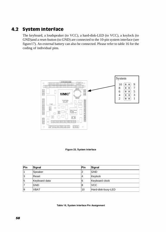
System InterfaceThe keyboard, a loudspeaker (to VCC), a hard-disk-LED (to VCC), a keylock (toGND)and a reset-button (to GND) are connected to the 10-pin system interface (seefigure17). An external battery can also be connected. Please refer to table 16 for thecoding of individual pins.
Figure 23, System Interface
Table 16, System Interface Pin Assignment
Pin Signal Pin Signal
1 Speaker 2 GND
3 Reset 4 Keylock
5 Keyboard data 6 Keyboard clock
7 GND 8 VCC
9 VBAT 10 Hard-disk-buxy-LED
System
97531
108642
4.2
59
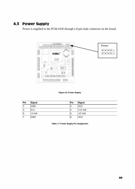
Power SupplyPower is supplied to the PCM-4330 through a 8-pin male connector on the board.
Power
12
Figure 24, Power Supply
Pin Signal Pin Signal
1 GND 2 VCC
3 N.C. 4 +12 Volt
5 -5 Volt 6 -12 Volt
7 GND 8 VCC
Table 17, Power Supply Pin Assignment
4.3

60
Floppy Disk InterfaceThe floppy disk interface is a coded 34-pin, 2-row male connector. Two (31/2 or51/4) floppy disk drives can be connected via a 34-wire flat cable. The odd pinsconnect the shielded wires to GND. Signals with # symbol are low active.
2
1
Floppy
Pin Signal I/O Function
2 HDS# O High Density Select
4 N.C. -
6 N.C. -
8 INDEX# I Index Hole
10 MO1# O Motor 1 On
12 DS2# O Drive 2 Select
14 DS1# O Drive 1 Select
16 MO2# O Motor 2 On
18 DIRC# O Direction
20 STEP# O Step Impulse
22 WD# O Write Data
24 WE# O Write Enable
26 TRK0# I Track 0
28 WP# I Write Protection
30 RDD# I Read Data
32 HS# O Head Select
34 DISKCHG# I Disk Change
Table 18, Floppy Disk Interface Pin Assignment
Figure 25,Floppy Disk Interface
4.4

61
IDE-/AT-Bus InterfaceThis is a coded 2-row 44-pin male connector on the board. Up to two IDE-/AT-Bus hard disk drives and/or IDE-/AT-bus CD-ROM drives can be connected viaa flat ribbon cable. Signals with # symbol are low active.
Pin Signal Pin Signal Pin Signal Pin Signal
1 RESET# 2 GND 23 IOW# 24 GND
3 D7 4 D8 25 IOR# 26 GND
5 D6 6 D9 27 N.C./IOCHRDY 28 BALE
7 D5 8 D10 29 N.C. 30 GND
9 D4 10 D11 31 IDINIT 32 IOCS16
11 D3 12 D12 33 SA1 34 N.C./MEMCS16#
13 D2 14 D13 35 SA0 36 SA2
15 D1 16 D14 37 CS# 38 HCS1#
17 D0 18 D15 39 HDLED 40 N.C.
19 GND 20 (coded) 41 VCC 42 VCC
21 N.C. 22 GND 43 GND 44 N.C.
Figure 26 , IDE-/AT-Bus
Table 19, IDE-/AT-Bus Pin Assignment
4.5
IDE-/AT-Bus
2 1
62
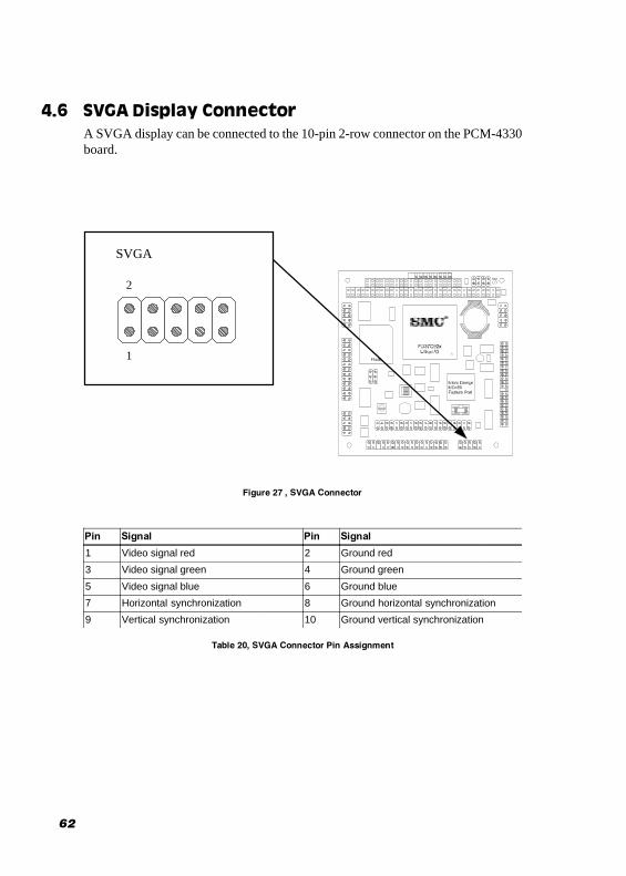
SVGA Display ConnectorA SVGA display can be connected to the 10-pin 2-row connector on the PCM-4330board.
SVGA
2
1
Figure 27 , SVGA Connector
Pin Signal Pin Signal
1 Video signal red 2 Ground red
3 Video signal green 4 Ground green
5 Video signal blue 6 Ground blue
7 Horizontal synchronization 8 Ground horizontal synchronization
9 Vertical synchronization 10 Ground vertical synchronization
Table 20, SVGA Connector Pin Assignment
4.6
63
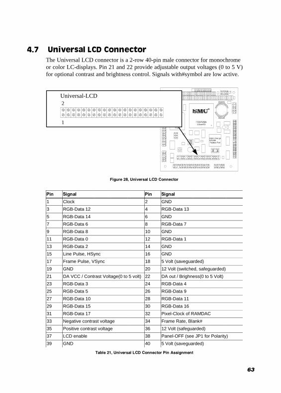
Universal LCD ConnectorThe Universal LCD connector is a 2-row 40-pin male connector for monochromeor color LC-displays. Pin 21 and 22 provide adjustable output voltages (0 to 5 V)for optional contrast and brightness control. Signals with#symbol are low active.
Universal-LCD2
1
Figure 28, Universal LCD Connector
Table 21, Universal LCD Connector Pin Assignment
Pin Signal Pin Signal
1 Clock 2 GND
3 RGB-Data 12 4 RGB-Data 13
5 RGB-Data 14 6 GND
7 RGB-Data 6 8 RGB-Data 7
9 RGB-Data 8 10 GND
11 RGB-Data 0 12 RGB-Data 1
13 RGB-Data 2 14 GND
15 Line Pulse, HSync 16 GND
17 Frame Pulse, VSync 18 5 Volt (saveguarded)
19 GND 20 12 Volt (switched, safeguarded)
21 DA VCC / Contrast Voltage(0 to 5 volt) 22 DA out / Brighness(0 to 5 Volt)
23 RGB-Data 3 24 RGB-Data 4
25 RGB-Data 5 26 RGB-Data 9
27 RGB-Data 10 28 RGB-Data 11
29 RGB-Data 15 30 RGB-Data 16
31 RGB-Data 17 32 Pixel-Clock of RAMDAC
33 Negative contrast voltage 34 Frame Rate, Blank#
35 Positive contrast voltage 36 12 Volt (safeguarded)
37 LCD enable 38 Panel-OFF (see JP1 for Polarity)
39 GND 40 5 Volt (saveguarded)
4.7
64
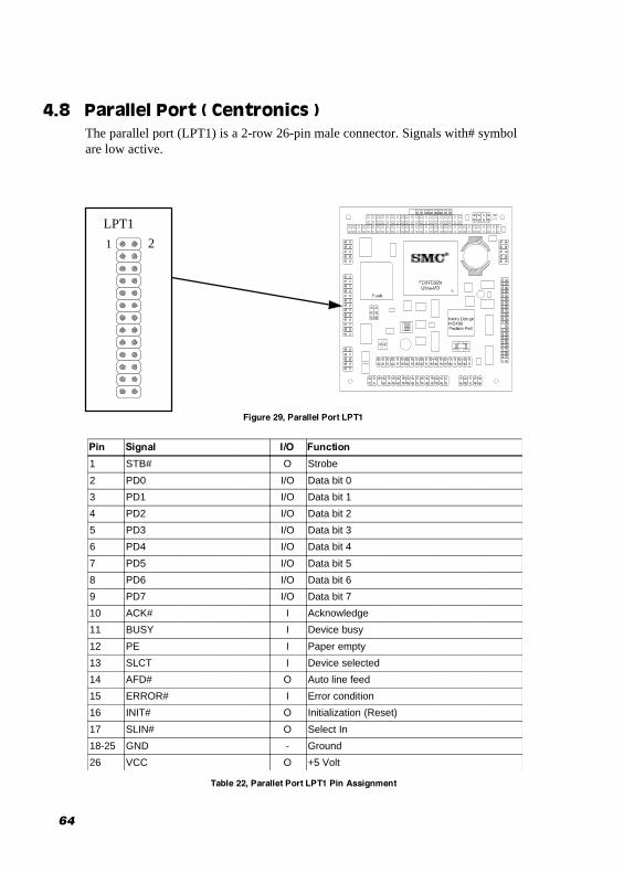
Parallel Port ( Centronics )The parallel port (LPT1) is a 2-row 26-pin male connector. Signals with# symbolare low active.
1 2
LPT1
Table 22, Parallet Port LPT1 Pin Assignment
Pin Signal I/O Function
1 STB# O Strobe
2 PD0 I/O Data bit 0
3 PD1 I/O Data bit 1
4 PD2 I/O Data bit 2
5 PD3 I/O Data bit 3
6 PD4 I/O Data bit 4
7 PD5 I/O Data bit 5
8 PD6 I/O Data bit 6
9 PD7 I/O Data bit 7
10 ACK# I Acknowledge
11 BUSY I Device busy
12 PE I Paper empty
13 SLCT I Device selected
14 AFD# O Auto line feed
15 ERROR# I Error condition
16 INIT# O Initialization (Reset)
17 SLIN# O Select In
18-25 GND - Ground
26 VCC O +5 Volt
Figure 29, Parallel Port LPT1
4.8

65
Serial PortsTwo serial RS-232-C interfaces (COM1 and COM2) are located on the PCM-4330PC/104 board computer as 2-row 10-pin male connectors.
COM1 & COM2
13579
246810
Pin Signal Function Pin Signal Function
1 DCD# Data Carrier Detect 2 DSR# Data Set Ready
3 RxD Receive Data 4 RTS# Request to Send
5 TxD Transmit Data 6 CTS# Clear to Send
7 DTR# Data Terminal Ready 8 RI# Ring Indicator
9 GND Ground 10 N.C. -
Figure 30, Serial Ports (COM1 and COM2)
Table 23, Serial Ports (COM1 and COM2) Pin Assignment
4.9

66
67
Software InterfacesThis chapter describes the software interface of the PCM-4330 PC/104 boardcomputer.
Address Summary of System MemoryA 1 MB address space is available in Real Mode and up to 4 MB physical memoryon-board in Protected Virtual Mode.After a system reset the CPU resumes operation in Real Address Mode. Codeat address FFFFF0h is executed next. Therefore, the BIOS area must be paged intothe upper 64 kB segment of the 4 MB address space. From there a far jump intosegment F000h is performed.
5
HEX Address Name Function
00000000h - 0009FFFFh 640 kB User RAMDOS applicationprograms
000A0000h - 000BFFFFh 128 kB Video RAM Display refresh memory
000C0000h - 000CBFFFh 40 kB VGA BIOS 40 kB Flash-Filings 8kB
000CC000h - 000EFFFFh 144 kB Extemsion ROM Extended BIOS area
000F0000h - 000FFFFFh 64 kB BIOS on-board BIOS area
00100000h - 003FFFFFhOn-board RAM4 MB
Extended Memory inProtected Mode only
00000000h - 00FFFFFFhOff-board RAM16 MB
On expansion boards (ifenabled in setup menu)
FFFF0000h - FFFFFFFFh 64 kB BIOS on-board BIOS area after reset
Table 24, Address Summary of System Memory
5.1

68
Interrupt Channels16 system interrupt channels are provided by the NMI of the CPU and two 8259interrupt controllers in the SIS-85C471-AT-Controller. All interrupts may bemasked. Interrupts are sorted by priority, starting with the highest priority. Table16 lists all available interrupts:
Interrupt Level Function
NMi Parity or I/O error
Master Slave
IRQ 0 Timer Output 0
IRQ 1 Keyboard
IRQ 2 Cascading for slave controller
IRQ 8 Real-time clock (RTC)
IRQ 9 Software redirect to INT 0Ah
IRQ 10 available
IRQ 11 available
IRQ 12 available
IRQ 13 Co-processor
IRQ 14 Hard disk controller
IRQ 15 available
IRQ 3 COM2
IRQ 4 COM1
IRQ 5 available (LPT2)
IRQ 6 Floppy disk controller
IRQ 7 LPT1
Table 25, System Interrupt Levels
5.2

69
DMA ChannelsThe PCM-4330 single board computer provides a total of seven DMA channels.Two 82c37-compatible DMA controllers in the SIS-85C471-AT-Controller are AT-compatibly cascaded as MASTER and SLAVE.
DMA Channel AssignmentChannel 0 of the Master-Controller (= DMA channel 4) is used to cascade input forthe Slave-Controller.Channels 0 to 3 (Slave) support 8-bit DMA data transfer between an 8-bit I/O unitand the 8/16-bit main memory. Channels 5 to 7 (Master 1 to 3) support 16-bit DMAdata transfer between a 16-bit I/O component and the 16-bit main memory.Channels 5 to 7 can only address data on even byte boundaries.
DMA Address GenerationThe limited addressing capability (16 address lines = 64 kB memory) of the 8237-DMA controller is extended to 16 MB by the Low-Page-Registers.The address is constituted by the contents of the Low-Page-Register and the DMAcontroller address in the current address register.
Port AThe SIS-85C471-AT-Controller. supports port A (I/O address 92h) of the PS/2®
system family. This offers a fast alternative to the PC/AT standard for controllingCPU resets and A20 control.
Port 92h Data Port Description
PS/2 RES RES RES RES RES RES A20 RST
x x x x x x r/w r/w
D7 D6 D5 D4 D3 D2 D1 D0
5.3
Bit Name Function7- 2 RES Reserved bits, always read “1”1 A20 Fast A20 shift
0 = A20-line always low1 = A20 under CPU control
0 RST Fast CPU reset0 = no reset initiated1 = initiate reset
5.3.1
5.3.2
5.4
70
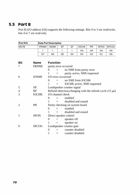
Port BPort B (I/O address 61h) supports the following settings. Bits 0 to 3 are read/write,bits 4 to 7 are read-only
5.5
Port 61h Data Port Description
KEYB PRNMI INOMI SP SF IOCHK PR SPON SPCOU
r r r r r/w r/w r/w r/w
D7 D6 D5 D4 D3 D2 D1 D0
Bit Name Function7 PRNMI parity error occurred
0 = no NMI from parity error1 = parity active, NMI requested
6 IONMI I/O error occurrend0 = no NMI from IOCHK1 = IOCHK active, NMI requested
5 SP Loudspesker counter signal4 RF Refresh detection,changing with the refresh cycle (15 µs)3 IOCHK I/O channel check
0 = enabled1 = disabled and erased
2 PR Parity checking on systom board0 = enabled1 = disabled and erased
1 SPON Direct speaker control0 = speaker off1 = speaker on
0 SPCOU Loudspeaker counter gate0 = counter disabled1 = counter disabled
71
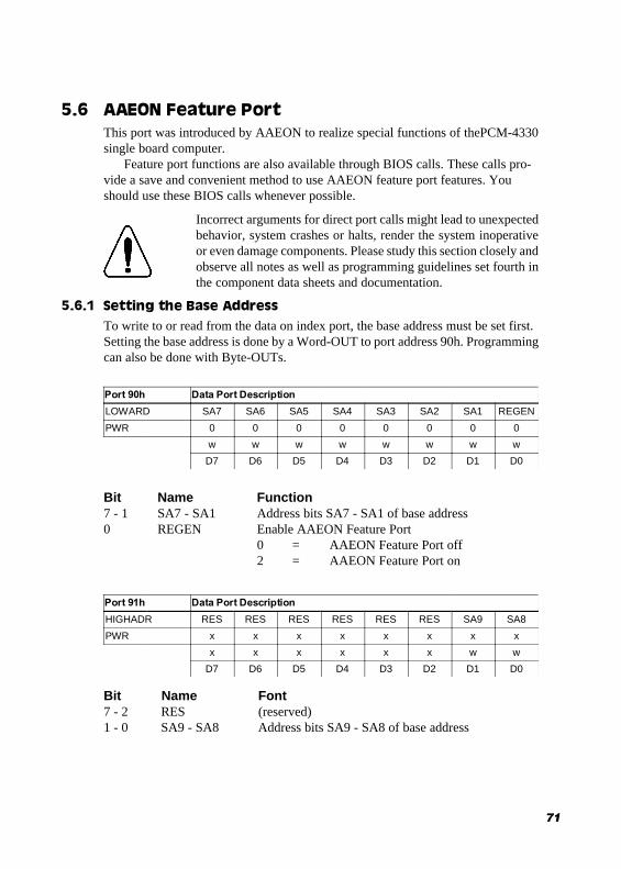
AAEON Feature PortThis port was introduced by AAEON to realize special functions of thePCM-4330single board computer. Feature port functions are also available through BIOS calls. These calls pro-vide a save and convenient method to use AAEON feature port features. Youshould use these BIOS calls whenever possible.
Incorrect arguments for direct port calls might lead to unexpectedbehavior, system crashes or halts, render the system inoperativeor even damage components. Please study this section closely andobserve all notes as well as programming guidelines set fourth inthe component data sheets and documentation.
Setting the Base AddressTo write to or read from the data on index port, the base address must be set first.Setting the base address is done by a Word-OUT to port address 90h. Programmingcan also be done with Byte-OUTs.
5.6.1
Port 90h Data Port Description
LOWARD SA7 SA6 SA5 SA4 SA3 SA2 SA1 REGEN
PWR 0 0 0 0 0 0 0 0
w w w w w w w w
D7 D6 D5 D4 D3 D2 D1 D0
Port 91h Data Port Description
HIGHADR RES RES RES RES RES RES SA9 SA8
PWR x x x x x x x x
x x x x x x w w
D7 D6 D5 D4 D3 D2 D1 D0
5.6
Bit Name Function7 - 1 SA7 - SA1 Address bits SA7 - SA1 of base address0 REGEN Enable AAEON Feature Port
0 = AAEON Feature Port off2 = AAEON Feature Port on
Bit Name Font7 - 2 RES (reserved)1 - 0 SA9 - SA8 Address bits SA9 - SA8 of base address

72
Feature Port Register Description
Data Port xxxxxxxxx0bThis port is used to write or read the data of the register set by the index port. Theaddress of the register and description of bits are found in the following table.
Index Port xxxxxxxxx1bThe index port is used to address the corresponding data register through whichthe data port is to be accessed.
MISCSET Register 0
Index: 0 Data Port Description
MISCSET 0 ID3 ID2 ID1 ID0 VPPEN RES WDEN RES
PWR 0 0 0 1 1 x 0 x
r r r r r/w x r/w x
D7 D6 D5 D4 D3 D2 D1 D0
5.6.2
Bit Name Function7-4 ID3-ID0 Identification code 4h in High-Nibble for AIO4863 VPPEN Activate programming voltage (12 Volt)
This bit also removes the write protection for allFlash and SRAM modules.0 = Programming voltage on1 = Programming voltage off(reserved)
2 RES Enable watchdog timer1 WDEN 0 = Watchdog off
1 = Watchdog on(reserved)
0 RES

73
MISCSET Register 1
Index: 1 Data Port Description
MISCSET 1 RES ROM CC V48K VGADIS VGARS RES RES
PWR x 0 0 0 0 0 x x
r r/w r/w r/w r/w r/w x x
D7 D6 D5 D4 D3 D2 D1 D0
Index: 2 Data Port Description
WDTRIG x x x x x x x x
PWR x x x x x x x x
x x x x x x x x
D7 D6 D5 D4 D3 D2 D1 D0
Bit Name Function7 RES (reserved)6 ROM Disable VGA-ROM at address C0000h
0 = VGA-ROM on1 = VGA-ROM off
5 CC Disable VGA-ROM at address C0000h0 = VGA-ROM on1 = VGA-ROM off
4 V48K Select VGA-ROM size0 = 48 kB1 = 32 kB
3 VGADIS Disable on-board VGA controller0 = WD90C24A on1 = WD90C24A off
2 VGARIS Disable on-board VGA controller0 = WD90C24A on1 = WD90C24A off
1 - 0 RES (reserved)
The watchdog timer is reset by a write operation to this register.
Watchdog Retrigger

74
A 10-bit AD converter from Linear Technology (LTC1392) is used on-board. Thiscomponent also contains a temperature sensor. The 5 V supply voltage is measuredinternally by a multiplexer of the LTC1392. Before the LTC1392. chip, an eightchannel multiplexer is put in line. This multiplexer measures several voltages on theboard. Please refer to the following table for the analog multiplexer input signals:
Channel 1 Programming voltage (12 Volt)Channel 2 12 VoltChannel 3 5 Volt (switched) voltage for LC-displayChannel 4 12 Volt (switched) voltage for LC-displayChannel 5 Keyboard voltage (5 Volt)Channel 6 Positive contrast voltage (max. 30 Volt)Channel 7 Negative contrast voltage (max. 30 Volt)Channel 8 Battery voltage (3 volt)
Before programming the LTC1390 or LTC1392. converters, please refer to the com-ponent data sheets.
DA Converter for LCD Contrast Control
Bit Name Function1 CS Chip select for multiplexer and AD converter0 DATA Data for multiplexer and from AD converter
Index: 6 Data Port Description
ADCTRL RES RES RES RES RES RES CS DATA
PWR x x x x x x x x
x x x x x x w r/w
D7 D6 D5 D4 D3 D2 D1 D0
AD Converter and Temperature Sensor
Bit Name Funtion1 LOAD Load impulse for DA converter0 DATA Data for DA converter
The DA converter used on-board is a 12-bit converter from Linear Technology(LTC1451). To avoid damaging the display, always check that the desired value issupported by the connected display.
Index: 5 Data Port Description
DACTRL RES RES RES RES RES RES LOAD DATA
PWR x x x x x x x 0
x x x x x x w r/w
D7 D6 D5 D4 D3 D2 D1 D0

75
MISCSET Register 2
Index: D Data Port Description
MISCSET 2 US05 US15 US012 US112 S5VEN S12VEN COMM1 COMM0
PWR 1 0 1 0 0 0 0 0
r/w r/w r/w r/w r/w r/w r/w r/w
D7 D6 D5 D4 D3 D2 D1 D0
Bit Name Function7 US05 Enable 5 Volt supply voltage for display through LCDEN pin
of the WD90C24 chip0 = Enable through LCDEN off1 = Enable through LCDEN on
6 US15 Enable 5 Volt supply voltage for display through PNLOFF pinof WD90C24 chip0 = Enable through PNLOFF off1 = Enable through PNLOFF on
5 US012 Enable 12 Volt supply voltage and contrast voltage for displaythrough delayed LCDEN signal of the WD90C24 chip0 = Enable through delayed LCDEN off1 = Enable through delayed LCDEN on
4 US112 Enable 12 Volt supply voltage and contrast voltage for displaythrough PNLOFF signal of the WD90C24 chip
0 = Enable through PNLOFF off1 = Enable through PNLOFF on
3 S5VEN Enable 5 Volt supply voltage for display0 = 5 Volt off1 = 5 Volt on
2 S12VEN Enable 12 Volt supply voltage and contrast voltage for display0 = 12 Volt off1 = 12 Volt on
1 COMM1 Select mode for COMB0 = RS232 mode1 = RS485 / RS422 mode
0 COMM0 Select mode for COMA0 = RS232 mode1 = RS485 / RS422 mode

76
BIT Name Function7 PROG Select on-board/external BIOS on ISA-bus
0 = External BIOS1 = On-board BIOS
6 - 5 RES (reserved)4 IRQ12 Enable PS/2 mouse interrupt on IRQ12
0 = IRQ12 disabled for PS/2 mouse1 = IRQ12 enabled for PS/2 mousePlease note: This function is not supported
on the PCM-4330 platform!3 COM Enable serial interface driver
0 = Interface driver off1 = Interface driver on
2 RES (reserved)1 SOUND Enable sound chip
0 = Sound chip off1 = Sound chip onPlease note: This function is not supported
on the PCM-4330 platform!0 NET Enable ethernet chip
0 = Ethernet chip off1 = Ethernet chip onPlease note: This function is not supported
on the PCM-4330 platform!
MISCSET Register 3
Index: E Data Port Description
MISCSET 3 PROG RES RES IRQ12 COM RES SOUND NET
PWR PROG x x 0 0 x 0 1
r/w x x r/w r/w x r/w r/w
D7 D6 D5 D4 D3 D2 D1 D0
Controller Revision
Index: F Data Port Description
REVISION ID3 ID2 ID1 ID0 REV3 REV2 REV1 REV0
PWR 0 0 0 1 x x x x
r r r r r r r r
D7 D6 D5 D4 D3 D2 D1 D0
Bit Name Function7 - 4 ID3 - ID0 Identification code 4h in High-Nibble for AIO4863 - 0 REV3 - REV0 Revision number for controller, currently 2h
77
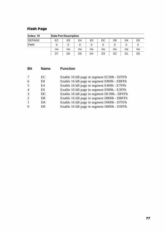
Flash Page
Index: 10 Data Port Description
DEPAGE EC E8 E4 E0 DC D8 D4 D0
PWR 0 0 0 0 0 0 0 0
r/w r/w r/w r/w r/w r/w r/w r/w
D7 D6 D5 D4 D3 D2 D1 D0
Bit Name Function
7 EC Enable 16 kB page m segment EC00h - EFFFh6 E8 Enable 16 kB page m segment E800h - EBFFh5 E4 Enable 16 kB page m segment E400h - E7FFh4 E0 Enable 16 kB page in segment E000h - E3FFh3 DC Enable 16 kB page in segment DC00h - DFFFh2 D8 Enable 16 kB page in segment D800h - DBFFh1 D4 Enable 16 kB page in segment D400h - D7FFh0 D0 Enable 16 kB page in segment D000h - D3FFh

78
Memory-Page 0
Index: 31 Data Port Description
PAGE0HI CARD0 A28 RES RES RES A24 A23 A22
PWR 0 0 x x x 0 0 0
r/w r/w x x x r/w r/w r/w
D7 D6 D5 D4 D3 D2 D1 D0
Index: 30 Data Port Description
PAGE0LO A21 A20 A19 A18 A17 A16 A15 A14
PWR 0 0 0 0 0 0 0 0
r/w r/w r/w r/w r/w r/w r/w r/w
D7 D6 D5 D4 D3 D2 D1 D0
Bit Name Function7 - 0 A21 - A14 Address for active page of memory module (16 KB)
Bit Name Function7 CARD0 Enable first 16 kB memory page
0 = Page disabled1 = Page enabled
6 A28 Address for active page of memory module (16 kB).This address determines, whether the on-board flash diskThis address determines, whether the on-board flash diskwidth) is used.0 = SIMM64/Flash/SRAM module (16 bit)1 = On-board flash disk (8 bit)Please note: Off-board modules are not supported
on the PCM-4330 platform.5 - 3 RES (reserved)2 - 0 A24 - A22 Address for active page of memory module (16 KB)
79
Memory-Page 1
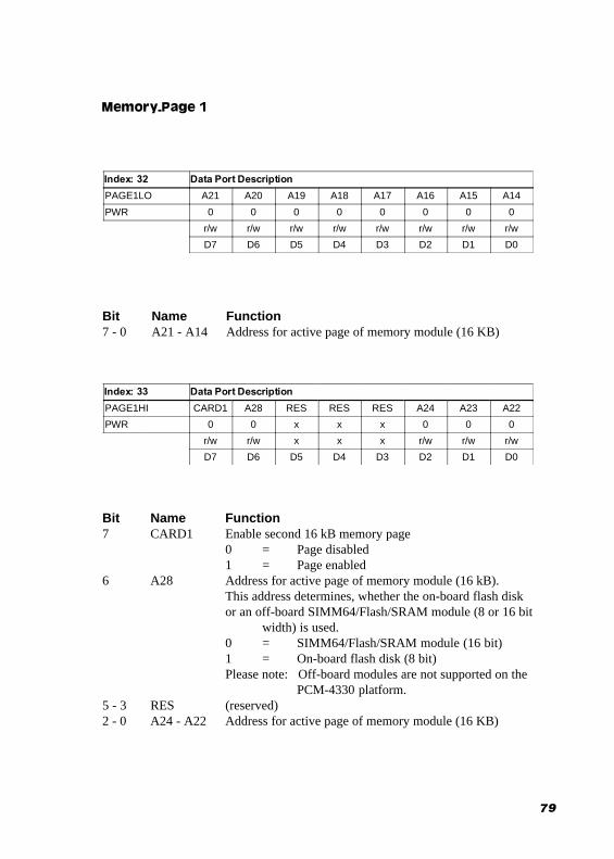
Index: 33 Data Port Description
PAGE1HI CARD1 A28 RES RES RES A24 A23 A22
PWR 0 0 x x x 0 0 0
r/w r/w x x x r/w r/w r/w
D7 D6 D5 D4 D3 D2 D1 D0
Index: 32 Data Port Description
PAGE1LO A21 A20 A19 A18 A17 A16 A15 A14
PWR 0 0 0 0 0 0 0 0
r/w r/w r/w r/w r/w r/w r/w r/w
D7 D6 D5 D4 D3 D2 D1 D0
Bit Name Function7 CARD1 Enable second 16 kB memory page
0 = Page disabled1 = Page enabled
6 A28 Address for active page of memory module (16 kB).This address determines, whether the on-board flash diskor an off-board SIMM64/Flash/SRAM module (8 or 16 bit
width) is used.0 = SIMM64/Flash/SRAM module (16 bit)1 = On-board flash disk (8 bit)Please note: Off-board modules are not supported on the
PCM-4330 platform.5 - 3 RES (reserved)2 - 0 A24 - A22 Address for active page of memory module (16 KB)
Bit Name Function7 - 0 A21 - A14 Address for active page of memory module (16 KB)
80
Memory-Page 2
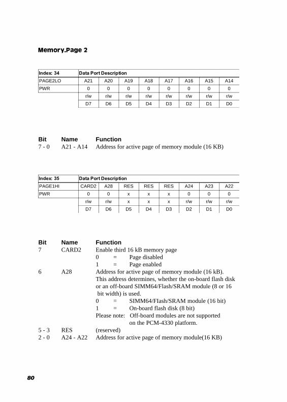
Index: 35 Data Port Description
PAGE1HI CARD2 A28 RES RES RES A24 A23 A22
PWR 0 0 x x x 0 0 0
r/w r/w x x x r/w r/w r/w
D7 D6 D5 D4 D3 D2 D1 D0
Index: 34 Data Port Description
PAGE2LO A21 A20 A19 A18 A17 A16 A15 A14
PWR 0 0 0 0 0 0 0 0
r/w r/w r/w r/w r/w r/w r/w r/w
D7 D6 D5 D4 D3 D2 D1 D0
Bit Name Function7 - 0 A21 - A14 Address for active page of memory module (16 KB)
Bit Name Function7 CARD2 Enable third 16 kB memory page
0 = Page disabled1 = Page enabled
6 A28 Address for active page of memory module (16 kB).This address determines, whether the on-board flash diskor an off-board SIMM64/Flash/SRAM module (8 or 16 bit width) is used.0 = SIMM64/FIash/SRAM module (16 bit)1 = On-board flash disk (8 bit)Please note: Off-board modules are not supported
on the PCM-4330 platform.5 - 3 RES (reserved)2 - 0 A24 - A22 Address for active page of memory module(16 KB)

81
Memory-page 3
Index: 37 Data Port Description
PAGE3HI CARD3 A28 RES RES RES A24 A23 A22
PWR 0 0 x x x 0 0 0
r/w r/w x x x r/w r/w r/w
D7 D6 D5 D4 D3 D2 D1 D0
Index: 36 Data Port Description
PAGE3LO A21 A20 A19 A18 A17 A16 A15 A14
PWR 0 0 0 0 0 0 0 0
r/w r/w r/w r/w r/w r/w r/w r/w
D7 D6 D5 D4 D3 D2 D1 D0
Bit Name Function7 - 0 A21 - A14 Address for active page of memory module(16kB)
Bit Name Function7 CARD3 Enable fourth 16 kB memory page
0 = Page disabled1 = Page enabled
6 A28 Address for active page of memory module (16 kB).This address determines. whether the on-board flash disk oran off-board SIMM64/Flash/SRAM module (8 or 16 bitwidth) is used.0 = SIMM64/Flash/SRAM module (16 bit)1 = On-board flash disk (8 bit)Please note: Off-board modules are not supported
on the PCM-4330 platform.5 - 3 RES (reserved)2 - 0 A24 - A22 Address for active page of memory module (16 KB)

82
Memory Address Space for Flash-/SRAM-Module
Bit Name Function7 - 4 RES (reserved)3 - 0 SA17- SA14 AT address space of first 16 kB window
SA19 and SA18 are assigned as logically high.Address spacemay be set in 16 kB increments.
Index: 38 Data Port Description
PCPAGE0 RES RES RES RES SA17 SA16 SA15 SA14
PWR x x x x 0 0 0 0
x x x x r/w r/w r/w r/w
D7 D6 D5 D4 D3 D2 D1 D0
Bit Name Function7 - 4 RES (reserved)3 - 0 SA17 - SA14 AT address space of third 16 kB window.
SA19 and SA18 are assigned as logically high.Address space may be set in 16 kB increments.
Bit Name Function7 - 4 RES (reserved)3 - 0 SA17 - SA14 AT address space of second 16 kB window.
SA19 and SA18 are assigned as logically high. Addressspace may be set in 16 kB increments.
Index: 3A Data Port Description
PCPAGE2 RES RES RES RES SA17 SA16 SA15 SA14
PWR x x x x 0 0 0 0
x x x x r/w r/w r/w r/w
D7 D6 D5 D4 D3 D2 D1 D0
Index: 39 Data Port Description
PCPAGE1 RES RES RES RES SA17 SA16 SA15 SA14
PWR x x x x 0 0 0 0
x x x x r/w r/w r/w r/w
D7 D6 D5 D4 D3 D2 D1 D0

83
Index: 3B Data Port Description
PCPAGE3 RES RES RES RES SA17 SA16 SA15 SA14
PWR x x x x 0 0 0 0
x x x x r/w r/w r/w r/w
D7 D6 D5 D4 D3 D2 D1 D0
PCM-4330 Register 0
Index: 40 Data Port Description
PWRDWN0 RES RES RES RES COM ESS SMC VGA
PWR x x x x 0 x x 0
x x x x r/w x x r/w
D7 D6 D5 D4 D3 D2 D1 D0
Bit Name Function7 - 4 RES (reserved)3 - 0 SA17 - SA14 AT address space of fourth 16 kB window.
SA19 and SA18 are assigned as logically high. Address spacemay be set in 16 kB increments.
Bit Name Function7 - 4 RES (reserved)3 COM PCM-4330 for LTC1334
through SMOUT 3 of SIS85C4710 = PCM-4330 off1 = PCM-4330 on
2 ESS PCM-4330 for ESSI788through SMOUT 3 of SIS85C4710 = PCM-4330 off1 = PCM-4330 onPlease note: This function is not supported
on the PCM-4330 platform!1 SMC PCM-4330 for SMC9IC92
through SMOUT 3 of SIS85C4710 = PCM-4330 off1 = PCM-4330 onPlease note: This function is not supported
on the PCM-4330 platform!0 VGA PCM-4330 for WD90C24
through SMOUT 0 of SIS85C4710 = PCM-4330 off1 = PCM-4330 on

84
Note to programmers: Accessing port 70h, databit 7 determines thestatus of the NMI controller:Bit 7 = 1, NMI disabledBit 7 = 0, NMI enabledThe desired control status for the NMI must be set for every applica-tion program accessing the RTC!
Address Description
00h Second 0-59
01h Seconds-Alarm 0-59
02h Minutes 0-59
03h Minutes-Alarm 0-59
04h Hours 1-12(24)
05h Hours-Alarm 0-23
06h Day of Week 1-7
07h Day of Month 1-31
08h Month 1-12
09h Year 0-99
0Ah Status Register A
0Bh Status Register B
0Ch Status Register C
0Dh Status Register D
0Eh-3Fh 50 bytes used by BIOS
40h-7Fh 2*64 bytes used by BIOS
Real-Time Clock/CMOS-RAMA MC146818A compatible, battery-buffered real-time clock (RTC) is included inthe DC37C92x-Ultra-I/O-controller. It provides data for time, alarm, control andstatus information. The remaining RAM is used by the BIOS to store system configu-ration data.
RTC/CMOS-RAM OperationsWriting into the RTC requires two steps:[1] Address output (OUT) at port70h[2] Data output (OUT) at port 71h
Table26 illustrates the internalRTC port addresses
To the programmer the RTCapears as a 128 byte RAM areathat can be addressed via two I/Oaddresses. 192 bytes RAM are inthis address-area. Two RAMpages are in area 40h to 3Fh whichmay be paged in/out alternatively.
RTC/CMOS-RAM Address Assignment
5.7
5.7.1
5.7.2
Table 26, RTC Address Assignment
i

85
System TimerThe system timer in the SIS-85C471-AT-Controller includes all 82C54 timer func-tions. It contains three AT-compatible, independently running and programmablecounters for software controlled generation of precise time intervals (counter 0, 1and 2)Counter 0 is connected to the interrupt request 0 of the Master-Interrupt-Controller.It has the highest priority of all maskable interrupts. Counter 0 has to interrupt theCPU every 50 ms to provide necessary time-updates. It is always active.Counter 1 works in mode 2, programmed to update the memory refresh logic every15 µs. Counter 1 is always active.Counter 2 operates in mode 3, programmed as a square-wave generator to controlthe speaker. It is controlled by gate 2 via System-Control-Latch-Bit 0 (I/O port61h). The output of counter 2 is combined by a logical and with bit 1 of the Port-B-Register to generate output signals for the speaker.
IO-Port Register Description
040hTimer 1, System Timer(Counter 0)
041hTimer 1, Refresh Request(Counter 1)
042hTimer 1, Speaker Tone(counter 2)
043hTimer 1, Control WordRegister
Table 28, Timer Register
5.8
Timer ProgrammingThe timer is addressed as a 8-bit periph-eral at I/O address 40h to 43h.Counters are programmed by writing thecontrol word and then the initial counterstate into the memory location of thecounter. Please refer to the SIS-85C471product documentation (Lit. [3]) for de-tailed information.
5.8.1
86
NMI Logic
After a Power-On-Reset the AT-NMI is disabled. By writing to I/O address 70h theAT-NMI can be enabled or disabled. Bit 7 can not be read.n Bit 7 = 1: AT-NMI disabledn Bit 7 = 0: AT-NMI enabled
The AT-NMI can be triggered by:n a parity error in the main memoryn the ISA-bus signal IOCHCK of an expansion card
Bits ENRAM and ENIOCK control the NMI sources via Port B.After a Power-On-Reset both NMI sources are enabled. Bits ENRAM and ENIOCKcan be read via Port B even if the AT-NMI is disabled. If an enabled parity error orI/O channel error occurs, the corresponding ENRAM or ENIOCK bit must be dis-abled and then enabled again to reset the logic.
Keyboard InterfaceFor the function of the keyboard interface, the controller is programmed to trans-late the codes received from the keyboard (Scan Codes) into system codes, whichcan be interpreted by the BIOS. The keyboard controller receives serial data fromthe keyboard, checks parity, translates key codes and sends the data to the systemas data byte into its output buffer. As soon as data is present in the buffer, an inter-rupt request (IRQ1) is asserted.Commands can be sent to the keyboard by writing into the buffer. The data byte issent to the keyboard as serial data with the uneven parity bit being inserted auto-matically. All data transmission to the keyboard must be acknowledged. No datamay be sent to the keyboard until the previous byte is acknowledged.
Floppy Disk ControllerA 765B-compatible SuperCellTM in the FDC37C92x-Ultra-I/O-controller from S MC(c.f. Lit. [4]) is used as floppy disk controller (FDC). Data is transferred over DMAchannel 2. Interrupts are triggered by IRQ6. Two floppy disk drives (3½ or 5¼ ) aresupported.
Floppy disks must be formatted according to their capacity. Failureto do so may result in read/write errors.
5.9
5.10
5.11

87
Parallel PortThe parallel centronics port is programmable (see Lit. [4]). It may operate in uni-directional mode (AT standard) or bi-directional mode. It contains the followingregisters:n Bi-directional parallel port for data transfern Status register for requests of the printer statusn Readback control register
Serial PortBoth serial RS-232-C ports are programmable via the FDC37C92x chip. This highlyintegrated chip features two independent channels for the AT-compatible 16550port. Each channel controls its own send/receive channel, has its own data registerand interrupts. Modem control signals are provided for each channel.
Programmable features are:n Serial data transmission with 5, 6, 7 or 8-bit charactersn Generation/detection of even, odd or no parityn Generation of 1,1.5 or 2 Stop-Bitsn Baud rate generator to divide the 1.8432 MHz clock frequency
5.12
5.13

88
89
6
6.1
6.1.1
FirmwareThis chapter describes the Award PowerBIOS functions of the PowerDwarf singleboard computer.
POST (Power On Self Test)After a (soft- or hardware) reset of the computer, a self-test and initializing of allhardware components is performed. This test is referred to as POST (Power On SelfTest) . After a hardware reset, on-screen messages identiftr which component is cur-rently being tested. If any errors occur during POST, a corresponding message isdisplayed on the screen. An error may occur due to hardware failure, i.e. an defec-tive component, or if the setup configuration is incorrect (e.g. setup informationcontains entries for two floppy disk drives while only one drive is actually installedin the system). Errors, that occur before the primary display adapter has been initialized, areindicated by the BIOS through a series of signals tones (beeps). Please refer tochapter G.I.I for the description of possible signals tones and their meaning. Afterthe display adapter initialization all errors are reported through on-screen error mes-sages. A description of error messages is found in chapter 6.I.2 on page 86. During POST, diagnostic codes are also written to I/O Port 80h. Chapter 6·I*3on page 89 lists possible diagnostic codes.
Signal Tone Error Messagesn 1 Beep: Refresh error
Check that the SIMM module is installed properly. If the error still occurs, re-place the memory chip.
n 2 Beeps: Parity errorCheck that the SIMM module is installed properly. If the error still occurs, re-place the memory chip.
n 3 Beeps: Error in the first 64 kB memory areaCheck that the SIMM module is installed properly. If the error still occurs, re-place the memory chip.
n 4 Beeps: as above, or the timer does not work The board must be replaced.n 5 Beeps: CPU error
The board must be replaced.n 6 Beeps: Gate Azo error
Check the keyboard controller and supply. Ifnecessary, replace the keyboardcontroller.
n 7 Beeps: CPU asserted unnecessary interruptThe board must be replaced.
90
n 8 Beeps: Video adapter errorReplace the video adapter or video adapter display memory RAM.n 9 Beeps: ROM-checksum errorThe BIOS will probably have to be replaced.n Io Beeps: CMOS-RAM register errorThe board must be replacedn 11 Beeps: Cache errorCheck the cache memory on the board.
On-screen Error Messagesif an error occurs during POST one or more of the following messages may appearon the display:
ERROR Message Line 1ERROR Message Line 2Press <F1> to continueThe program stops, if the setup option Halt On Ewors is set to All ewors.
Alternatively, the program might prompt you to run the setup utility program tocorrect settings. The following message would be displayed on-screen:
RUN SETUP UTILITYThe following section describes error messages, provides explanations and suggestswork-arounds. Further POST messages and problem work-arounds can be found inthe reference documents.
8042 Gate-A20 ErrorThe keyboard controller gate Azo does not work properly. Replace the keyboardcontroller.
Address Line Short!Address coding error.
C: Drive ErrorDrive C: does not respond. Use the diagnostic utility program AM~Diag Hard DiskUtility to test the drive and check that all hard disk drive parameters and hard disksetup settings are correct.
C: Drive FailureDrive C: does not respond. Replace the hard disk drive.
Cache Memory bad. Do Not enable Cache!The cache memory is corrupt. Run the AMIDiag diagnostic utility program.
CH-2 Timer ErrorTimer 2 error.
6.1.2

91
CMOS Battery State LowThe CMOS-RAM is (almost) empty.
CMOS Checksum Failure CMOS-RAMThe checksum does not contain a valid value. Use the setup program to calculate avalid checksum.
CMOS System Options Not SetCMOS-RAM values are false or non-existent. Use the setup program to identiftrand correct the problem.
CMOS Display Type MismatchThe CMOS-RAM video adapter type setting does not correspond to the displayadapter installed. Run the setup utility program to correct the problem.
CMOS Memory Size MismatchThe size of memory installed does not correspond to the CMOS-RAM setting. Runthe setup utility program to check settings.
CMOS Time and Date Not SetRun the setup utility program to enter new time and date values.
D: Drive ErrorDrive D: does not respond. Use the diagnostic utility program AM~Diag Hard DiskUtility to test the drive and check that all hard disk drive parameters and hard disksetup settings are correct.
D: Drive FailureDrive D: does not respond. Replace the hard disk drive.
Diskette Boot FailureThe disk in drive A: is not a boot disk. Insert a boot disk and following directions onthe screen.
Display Switch Not ProperSome computer system use display type switches to set the display type to mono-chrome or color. Check the stting off this switch or jumper.
DMA ErrorDMA controller error.
DMA 1 Error or DMA 2 ErrorDMA channel error.

92
FDD Controller FailureBIOS could not address the floppy disk controller. Check that all cables are prop-erly connected.
HDD Controller FailureBIOS could not address the hard disk controller. Check that all cables are connectedproperly.
INTR 1 Error orINTR 2 ErrorInterrupt channel error.
Invalid Boot DisketteBIOS could read the disk but could not boot the system from the disk. Insert anotherboot disk and follow directions on the screen.
Keyboard Is Locked...Unlock ItThe keyboard is locked (keyswitch).
Keyboard ErrorThe keyboard obviously has timing problems.
KB/Interface ErrorThe keyboard is not connected properly.
No ROM BASICBIOS could not find a free sector on drive A: or on the hard disk for the bootoperation.
Off Board Parity ErrorA memory parity error has occurred on an adapter board.
On Board Parity ErrorA memory parity error has occurred on the board.
Parity Error ????A memory parity error has occurred at an unidentified location.

93
Table 28, POST - Code
POST-Codes
During the Power On SeEfTest, POST codes are sent to I/O port 80h. Each routinenumber (hexadecimal) is sent to the post Port before the routine is called. The fol-lowing table lists all possible POST codes:
Co de Fu nctio n Descr iptio n
00h (None) Hook for Cpu type detec tion (CPU extens ion)
01h Ti mer R eset Init ializes the tim er
02h D MA R eset Ini tial izes the D MA control ler
03h IR Q POST Init iali zes the interrupt control ler
04h RT C R eset Init ializes R TC control regis ters
05h KBD R eset Init ializes the k ey board Error codes : BAh...BFh
06h Video Blank Clears screen (if 684~ pr esent)
07h NVS Checksum Calculates CMOS c hecksum
08h N VS Default Ini ti alize s C MOS if checksum bad
09h ROM Checks umCal culates ROM checks um, sys tem halted ifchecksum bad
10h M emory Siz ing C hecks memor y pr esenc e, saves s ize in C MOS
11h POST Setup Init ializes memor y, s ets i nterr upt vec tors
12h Setup Opt ion R OM Init ial izes opt ion R OM table
15h Tim er Test Enabl es tim er IRQ (INT8)
16h NC P POST Detec ts co-processor
17h KBD SetupSet up keyboard varia bles (in data area),enables key board IRQ (INT9)
18h Vide o POST Initi alizes ISA v ideo if presen
19h Optio n POSTDetects non-v ideo opt ion R OM s, s tores r inopt ion ROM table
1Ah Display POST Set up POST window, di splays early results
25h (None)PS/2 m ouse i nit hooks here i f PS2M ex tens ionis present
26h F loppy POST Detec ti on and init ial izat ion of f loppy disk drives
27h (None)IDE hard disk ini t hook s here if F IXED ex tens ionis present
28h Serial POST Detec tion and init iali zat ion of serial ports
29h Parallel POST Detec t ion and ini ti alization of parallel ports
6.1.3

94
Table 28, POST - Codes
C o d e F u n c t i o n D e s c r i p t i o n
2 A h G a m e P o r t P O S T D e t e c tio n o f g a m e p o r t
2 B h R T C P O S T C o p ie s c u r re n t R T C t im e in B I O S d a t a a re a( BD A )
2 D h R A M P O S T M e m o ry t e st
4 0 h C h e c ks u m R e ca lc u la t e s C M O S c h e c ks u m
4 1 h Op t io n R O M I n it I n iti a liz e s a l l n o n -v id e o I S A o p t io n R OM s st o re din o p t io n R O M t a b le
4 F h B o o t P O S T A tt e m p t t o b o o t
5 0 h (N o n e ) R e st a r t
D E h (N o n e ) P o w e r -o n o r h a rd w a re re se t
6 x h P O S T S h u t d o w n R e s ta r t c a u s e d b y so f t w a re , x in d ic a te ssh u t d o w n ty p e
5 1 h P O S T S h u t d o w n I n va l id sh u td o w n t yp e d e t e c te d , s ys te m h a lt e d
C F h P O S T B e g in E a r l y in i t, b e g i n e xe c u t io n o f P O S T r o u tin e s
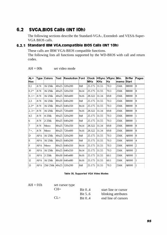
95
SVGA-BIOS Calls (INT l0h)The following sections describe the Standard-VGA-, Extended- and VESA-Super-VGA BIOS calls.
Standard IBM VGA-compatible BIOS Calls (INT 10h)These calls are IBM VGA-BIOS compatible functions.The following lists all functions supported by the WD-BIOS with call and returncodes.
AH = 00h set video mode
AL=
Hex
Type Colors Text Resolution Font Clock
MHz
HSync
KHz
VSync
Hz
Min.
memo
Brffer
Start
Pages
0,1 A/N 16/256k 40x25 320x200 8x8 25.175 31.55 70.3 256K B8000 8
0,1* A/N 16/256k 40x25 320x350 8x14 25.175 31.55 70.3 256K B8000 8
0,1+ A/N 16/256k 40x25 360x400 9x16 28.322 31.34 69.8 256K B8000 8
2,3 A/N 16/256k 80x25 640x200 8x8 25.175 31.55 70.3 256K B8000 8
2,3* A/N 16/256k 80x25 640x350 8x14 25.175 31.55 70.3 256K B8000 8
2,3+ A/N 16/256k 80x25 720x400 9x16 28.322 31.34 69.8 256K B8000 8
4,5 A/N 4/256k 40x25 320x200 8x8 25.175 31.55 70.3 256K B8000 1
6 A/N 2/256k 80x25 640x200 8x8 25.175 31.55 70.3 256K B8000 1
7 A/N Mono 80x25 720x350 9x14 28.322 31.34 69.8 256K B8000 8
7+, A/N Mono 80x25 720x400 9x16 28.322 31.34 69.8 256K B8000 8
D APA 16/256k 40x25 320x200 8x8 25.175 31.55 70.3 256K A0000 8
E APA 16/256k 80x25 640x200 8x8 25.175 31.55 70.3 256K A0000 4
F APA Mono 80x25 640x350 8x14 25.175 31.55 70.3 256K A0000 2
10 APA 16/256k 80x25 640x350 8x14 25.175 31.55 70.3 256K A0000 2
11 APA 2/256k 80x30 640x480 8x16 25.175 31.55 60.1 256K A0000 1
12 APA 16/256k 80x30 640x480 8x16 25.175 31.55 60.1 256K A0000 1
13 APA 256/256k 40x25 320x200 8x8 25.175 31.55 70.3 256K A0000 1
AH = 01h set cursor typeCH=
CL=
Bit 0..4 start line or cursorBit 5..6 blinking attributesBit 0..4 end line of cursors
Table 30, Supported VGA Video Modes
6.2
6.2.1

96
AH = 02h set cursor positionDH = lineDL = rowscreen page numberBH = 0 in graphics mode
0..3 in mode 2/30..7 in mode 0/1
AH = 03h read cursor positionBH = screen page number
0 in graphics mode0..3 in mode 2/30..7 in mode 0/1
DH: = lineDL: = rowCH: = start line of cursorCL: = end line of cursor
AH = 05h select active screen page numberAL = screen page number
0..3 in mode 2/30..7 in mode 0/1
AH = 06h scroll up sector of active screenAL = number of lines to scroll (0 for all lines of screen)BH = attribute for lines to deleteCH = line of upper left corner of the sectorCL = row of upper left comer of the sectorDH = line of lower right comer of the sector
DL = row of lower right comer of the sector
AH = 07h scroll down sector of active screenAL = number of lines to scroll (0 for all lines of screen)BH = attribute for lines to deleteCH = line of upper left corner of the sectorCL = row of upper left comer of the sectorDH = line of lower right comer of the sectorDL = row of lower right comer of the sector
AH = 08h read character and attribute at cursor positionBH = screen page numberAL: = character at cursor positionAH: = attribute of character at cursor position
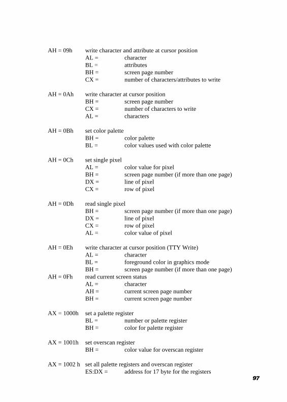
97
AH = 09h write character and attribute at cursor positionAL = characterBL = attributesBH = screen page numberCX = number of characters/attributes to write
AH = 0Ah write character at cursor positionBH = screen page numberCX = number of characters to writeAL = characters
AH = 0Bh set color paletteBH = color paletteBL = color values used with color palette
AH = 0Ch set single pixelAL = color value for pixelBH = screen page number (if more than one page)DX = line of pixelCX = row of pixel
AH = 0Dh read single pixelBH = screen page number (if more than one page)DX = line of pixelCX = row of pixelAL = color value of pixel
AH = 0Eh write character at cursor position (TTY Write)AL = characterBL = foreground color in graphics modeBH = screen page number (if more than one page)
AH = 0Fh read current screen statusAL = characterAH = current screen page numberBH = current screen page number
AX = 1000h set a palette registerBL = number or palette registerBH = color for palette register
AX = 1001h set overscan registerBH = color value for overscan register
AX = 1002 h set all palette registers and overscan registerES:DX = address for 17 byte for the registers
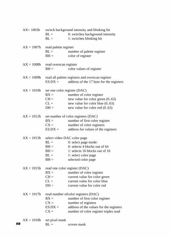
98
AX= 1003h switch background intensity and blinking bitBL = 0: switches background intensityBL = 1: switches blinking bit
AX = 1007h read palette registerBL = number of palette registerBH = color of register
AX = 1008h read overscan registerBH = color values of register
AX = 1009h read all palette registers and overscan registerES:DX = address of the 17 byte for the registers
AX = 1010h set one color register (DAC)BX = number of color registerCH = new value for color green (0..63)CL = new value for color blue (0..63)DH = new value for color red (0..63)
AX = 1012h set number of color registers (DAC)BX = number of first color registerCX = number of color registersES:DX = address for values of the registers
AX = 1013h select video DAC color pageBL = 0: select page mode:BH = 0: selects 4 blocks out of 64BH = 1: selects 16 blocks out of 16BL = 1: select color pageBH = selected color page
AX = 1015h read one color register (DAC)BX = number of color registerCH = current value for color greenCL = current value for color blueDH = current value for color red
AX = 1017h read number ofcolor registers (DAC)BX = number of first color registerCX = number of registersES:DX = address of the values for the registersCX = number of color register triples read
AX = 1018h set pixel maskBL = screen mask
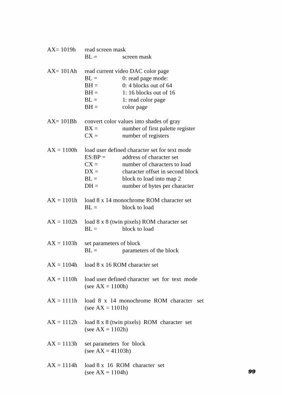
99
AX= 1019h read screen maskBL = screen mask
AX= 101Ah read current video DAC color pageBL = 0: read page mode:BH = 0: 4 blocks out of 64BH = 1: 16 blocks out of 16BL = 1: read color pageBH = color page
AX= 101Bh convert color values into shades of grayBX = number of first palette registerCX = number of registers
AX = 1100h load user defined character set for text modeES:BP = address of character setCX = number of characters to loadDX = character offset in second blockBL = block to load into map 2DH = number of bytes per character
AX = 1101h load 8 x 14 monochrome ROM character setBL = block to load
AX = 1102h load 8 x 8 (twin pixels) ROM character setBL = block to load
AX = 1103h set parameters of blockBL = parameters of the block
AX = 1104h load 8 x 16 ROM character set
AX = 1110h load user defined character set for text mode(see AX = 1100h)
AX = 1111h load 8 x 14 monochrome ROM character set(see AX = 1101h)
AX = 1112h load 8 x 8 (twin pixels) ROM character set(see AX = 1102h)
AX = 1113h set parameters for block(see AX = 41103h)
AX = 1114h load 8 x 16 ROM character set(see AX = 1104h)

100
AX = 1120h load user defined 8 x 8 graphic character set (INT 1Fh)ES:BP= address of character setload user definedcharacter set
AX = 1121h ES:BP= address of character setCX= number of bytes per characterBL= information about the number of lines on the
screen page0: DL defines number of lines1:14 lines2:25 lines3:43 lines
AX = 1122h load 8 x 14 ROM graphics character setBL= information about number of lines
AX = 1123h load 8 x 8 (twin pixels) ROM graphics character setBL= information about number of linesAX = 1124h load 8 x 16 ROM graphics character set
BL= information about number of linesAX = 1130h return information on current character set
ES:BP= address of pointer to character setCX= number of bytes per character in character setDL= number of lines on the screen page
AH = 12h BL=10h return video informationBH= color or monochrome mode (0: color mode)BL= size of screen memory in 64 byte stepsCL= switch setting
AH = 12h BL=20h switch to alternative functions for screen printAH = 12h BL=30h set vertical screen resolution
AL= number of vertical lines0:200 lines1:350 lines2:400 lines
AL= 12h (since function is supported)AH = 12h BL=31h load standard values for palette registers
AL= enable/disable loading of standard values forpalette registers
AL= 12h (since function is supported)AH = 12h BL=32h enable/disable video addressing
AL= enable/disable video addressingAL= 12h (since function is supported)

101
AH = 12h BL=33h conversion color to grayscaleAL= enable/disable conversion of color values to grayscaleAL= 12h (since function is supported)
AH = 12h BL=34h cursor emulationAL= enable/disable cursor emulationAL= 12h (since function is supported)
AH = 12hBL=35h monitor switchingAL= type of switchingES:DX= 128 byte array to store old video valuesAL = 12h (since function is supported)
AH = 12h BL=36h monitor on/off
AH = 13h write textAL= Mode (move cursor / additional attributes for text)BL= attribute (if not included in the text)BH= screen page numberDH= write text in lineDL= write text in columnCX= length of textES:BP= address of text
AX = 1A00h read video codesBL= current video codeBH= alternate video codeAL= 1Ah (since function is supported)
AX = 1A01h write video codeBL= current video codeBH= alternate video codeAL= 1Ah (since function is supported)
AH = 1BhA read status informationBX= type (0000h)ES:DI= 64 byte buffer for status informationAL= 1Bh (since function is supported)
X = 1C00h read size of buffer for video statusCX= which video statusBX= size of buffer in 64 byte blocksAL= 1Ch (since function is supported)
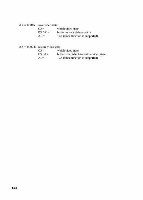
102
AX = 1C01h save video stateCX= which video stateES:BX = buffer to save video state inAL = 1Ch (since function is supported)
AX = 1C02 h restore video stateCX= which video stateES:BX= buffer from which to restore video stateAL= 1Ch (since function is supported)
103
Extended BIOS Calls (INT 10h)These calls are spedtic to the WD-BIOS.The following lists functions that are supported by the WD-BIOS with calland return codes.
6.2.2
AX = 7F7Fh BH = 00h set non-VGA mode
AX = 7F7Fh BH = 01h set VGA mode
AX = 7F7Fh BH = 02h read spedtic status informationCH= number of available 64 KB blocks of screen memoryCL= number of used blocks
AX = 7F7Fh BH = 03h disable current VGA modeBL= enable/disable current VGA mode
AX = 7F7Fh BH = 04h set non-VGA MDA (monochrome) mode
AX = 7F7Fh BH = 05h set non-VGA CGA (color) mode
AX = 7F7Fh BH = 06h set VGA monochrome mode
AX = 7F7Fh BH = 07h set VGA color mode
AX = 7F7Fh BH = 08h disable RAMDACBL= enable/disable RAMDAC
AX = 7F7Fh BH = 22h read BitBLT scroll status informationBL= hardware BitBLT or software scroll-function
0: hardware BitBLT scroll-function1: software scroll-function
AX = 7F7Fh BH = 23h set BitBLT scroll-functionBL= 0: hardware BitBLT scroll-function
1: software scroll-function
AX = 7F7Fh BX = 4100h enable LCD- and CRT-monitorAX = 7F7Fh BX = 4101h enable or disable auto-centering
This function is not available if vertical expansionis actived.
AX = 7F7Fh BX = 4102h toggle vertical expansionThis function is available for video modes 3+ and7+ only.
104
Bit Description
0,1 (reserved)
2 0:1:
CRT displayLCD display
3 0:1:
autocentering onartocentering off
5,4 00:01:10:11:
normal graphics and inverted textnormal graphics and mormal textinverted graphics and text(reserved)
6 0:1:
vertical expansion onvertical expansion off
9,8 00:01:10:11:
800x600 pixel at 56 Hz800x600 Pixel at 60 Hz800x600 pixel at 72 Hz800x600 pixel (16 colors) at 72 Hz and800x600 pixel (256 colors) at 60 Hz
11,10 00:01:
1024x768 pixel (16 colors) interlaced1024x768 pixel (16 colors) at 60 Hz
13,12 00:01:
1024x768 pixel (256 colors) interlaced1024x768 pixel (256 colors) at 60 Hz
14 0:1:
no simultaneous display on CRT / LCDsimultaneous display on CRT and LCD
15 (reserved)
Table 30, INT 10h AX= 7F7Fh / BX = 4200h, Return Extended Status Information
AX = 7F7Fh BX = 4104h toggle displayToggle between LCD, CRT or simultaneous displayon LC and CRT. For high resolution video modeswhich are not sup ported by the LC-display. simul-aneous display cannot be selected.
AX = 7F7Fh BX = 4105h enable CRT-monitor
AX = 7F7Fh BX = 4106h enable LCD-monitor
AX = 7F7Fh BX = 4107h switch between LCD- and CRT-monitor
AX = 7F7Fh BX = 4108h toggle simultaneous/non-simultaneous display
AX = 7F7Fh BX = 410Ah switch between normal/inverted text display
AX = 7F7Fh BX = 410Bh switch between normal/inverted graphics display
AX = 7F7Fh BX = 410Dh switch to simultaneous display
AX = 7F7Fh BX = 4200h return extended status informationBX= status information

105
Bit Description
0,1 (reserved)
2 0:1:
CRT displayLCD display
3 0:1:
autocentering onartocentering off
5,4 00:01:10:11:
normal graphics and inverted textnormal graphics and mormal textinverted graphics and text(reserved)
6 0:1:
vertical expansion onvertical expansion off
9,8 00:01:10:11:
800x600 pixel at 56 Hz800x600 Pixel at 60 Hz800x600 pixel at 72 Hz800x600 pixel (16 colors) at 72 Hz and800x600 pixel (256 colors) at 60 Hz
11,10 00:01:
1024x768 pixel (16 colors) interlaced1024x768 pixel (16 colors) at 60 Hz
13,12 00:01:
1024x768 pixel (256 colors) interlaced1024x768 pixel (256 colors) at 60 Hz
14 0:1:
no simultaneous display on CRT / LCDsimultaneous display on CRT and LCD
15 (reserved)
Table 31, INT 10h AX= 7F7Fh / BX = 4201 h, Set Extended Status Information
AX= 7F7Fh BX = 4201h set extended status information CX= status information
AX = 7F7Fh BX=4300h set power-on conditionCX= value for INT 15h call (CMOS-value)
AX = 7F7Fh BX=4400h return power-on conditionBL= value of power-on condition
AX = 7F7Fh BX=4500h return version numbers of VGA BIOSBL= 1. digit of version numberCH= 2. digit of version numberCL= 3. digit of version number
AX = 7F7Fh BX=4700h return type of connected monitor (dynamic)BX= status informationCX= status information

106
AL=
HEX
WD
Modus
Type Colors Text Resolution Font Min.
Memory
Buffer
Start
Pages
100 5E APA 256/256K 80x25 640x400 8x16 512K A0000 1
101 5F APA 256/256K 80x30 640x480 8x16 512K A0000 1
102 58/6A APA 16/256K 100x75 800x600 8x8 256K A0000 1
103 5C APA 256/256K 100x75 800x600 8x8 512K A0000 1
104 5D APA 16/256K 128x48 1024x768 8x16 512K A0000 1
105 60 APA 256/256K 128x48 1024x768 8x16 1M A0000 1
109 55 APA 16/256K 132x25 1056x400 8x16 256K B8000 4
10A 54 APA 16/256K 132x43 1056x344 9x9 256K B8000 2
10D 68 APA 32768 40x25 320x200 8x8 256K A0000 1
10E 78 APA 65536 40x25 320x200 8x8 256K A0000 1
110 62 APA 32768 80x30 640x480 8x16 1M A0000 1
111 72 APA 65536 80x30 640x480 8x16 1M A0000 1
VESA SuperVGA 8105 Calls (INT 1Oh)These calls are VESA SuperVGA-BIOS specific.The following lists functions that are supported by the WD-BIOS with call andreturn codes.
AH = 00h set video mode
6.2.3
Table 32, Supported VESA Super VGA Video Modes
AX = 4F00h return SuperVGA informationES:DI =256 Byte buffer for SuperVGA informationAL= 00h: 4 Byte text string "VESA"AH= 004h: Word VESA version number
006h: DWord pointer to OEM-name00Ah: 4 Byte properties00Eh: DWord pointer to supported VESA and OEM12h: display modes
(reserved from here)4Fh (since function is supported)00h:OK (buffer filled with Super VGA information)01h:error
AX = 4F01h return SuperVGA mode informationCX = SuperVGA screen modeES:DI= 256 Byte buffer for SuperVGA mode informationAL= 4Fh (since function is supported)AH= 00h: OK (buffer filled with SuperVGA mode informa-
tion)01h: error
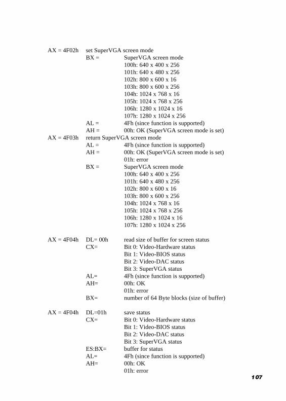
107
AX = 4F02h set SuperVGA screen modeBX = SuperVGA screen mode
100h: 640 x 400 x 256101h: 640 x 480 x 256102h: 800 x 600 x 16103h: 800 x 600 x 256104h: 1024 x 768 x 16105h: 1024 x 768 x 256106h: 1280 x 1024 x 16107h: 1280 x 1024 x 256
AL = 4Fh (since function is supported)AH = 00h: OK (SuperVGA screen mode is set)
AX = 4F03h return SuperVGA screen modeAL = 4Fh (since function is supported)AH = 00h: OK (SuperVGA screen mode is set)
01h: errorBX = SuperVGA screen mode
100h: 640 x 400 x 256101h: 640 x 480 x 256102h: 800 x 600 x 16103h: 800 x 600 x 256104h: 1024 x 768 x 16105h: 1024 x 768 x 256106h: 1280 x 1024 x 16107h: 1280 x 1024 x 256
AX = 4F04h DL= 00h read size of buffer for screen statusCX= Bit 0: Video-Hardware status
Bit 1: Video-BIOS statusBit 2: Video-DAC statusBit 3: SuperVGA status
AL= 4Fh (since function is supported)AH= 00h: OK
01h: errorBX= number of 64 Byte blocks (size of buffer)
AX = 4F04h DL=01h save statusCX= Bit 0: Video-Hardware status
Bit 1: Video-BIOS statusBit 2: Video-DAC statusBit 3: SuperVGA status
ES:BX= buffer for statusAL= 4Fh (since function is supported)AH= 00h: OK
01h: error

108
AX = 4F04h DL = 02h load saved statusCX= Bit 0: Video-Hardware status
Bit 1: Video-BIOS statusBit 2: Video-DAC statusBit 3: SuperVGA status
ES:BX= buffer where status is savedAL= 4Fh (as function is supported)AH= 00h: OK
00h: OK01h: error
AX = 4F05h BH=00h select memory screen windowBL= 00h: window A
01h: window Baddress of window in screen memory (units)
DX= 4Fh (since function is supported)AL= 00h: OKAH= 01h: error
AX = 4F05h BH=01h return memory screen windowBL= 00h: window A
01h: window Baddress of window in screen memory (units)
DX= 4Fh (since function is supported)AL= 00h: OKAH= 01h: error
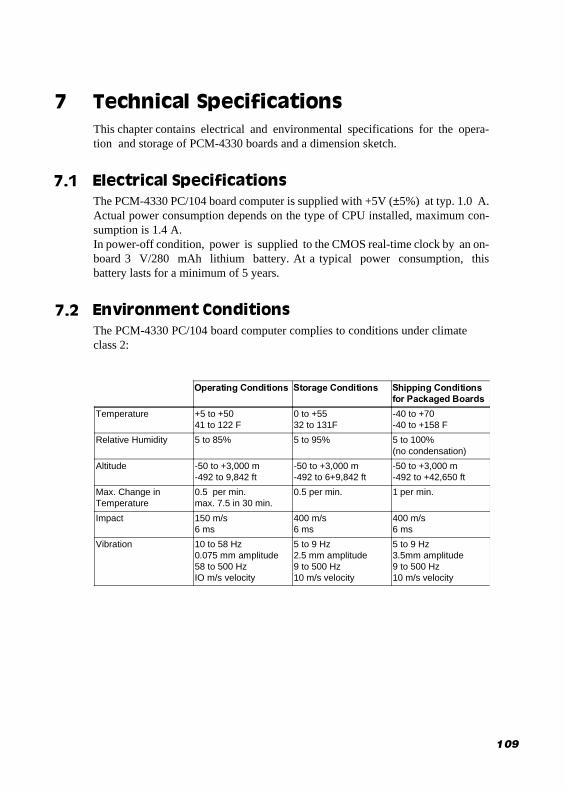
109
Technical SpecificationsThis chapter contains electrical and environmental specifications for the opera-tion and storage of PCM-4330 boards and a dimension sketch.
Electrical SpecificationsThe PCM-4330 PC/104 board computer is supplied with +5V (±5%) at typ. 1.0 A.Actual power consumption depends on the type of CPU installed, maximum con-sumption is 1.4 A.In power-off condition, power is supplied to the CMOS real-time clock by an on-board 3 V/280 mAh lithium battery. At a typical power consumption, thisbattery lasts for a minimum of 5 years.
Environment ConditionsThe PCM-4330 PC/104 board computer complies to conditions under climateclass 2:
7
Operating Conditions Storage Conditions Shipping Conditions
for Packaged Boards
Temperature +5 to +5041 to 122 F
0 to +5532 to 131F
-40 to +70-40 to +158 F
Relative Humidity 5 to 85% 5 to 95% 5 to 100%(no condensation)
Altitude -50 to +3,000 m-492 to 9,842 ft
-50 to +3,000 m-492 to 6+9,842 ft
-50 to +3,000 m-492 to +42,650 ft
Max. Change inTemperature
0.5 per min.max. 7.5 in 30 min.
0.5 per min. 1 per min.
Impact 150 m/s6 ms
400 m/s6 ms
400 m/s6 ms
Vibration 10 to 58 Hz0.075 mm amplitude58 to 500 HzIO m/s velocity
5 to 9 Hz2.5 mm amplitude9 to 500 Hz10 m/s velocity
5 to 9 Hz3.5mm amplitude9 to 500 Hz10 m/s velocity
7.1
7.2
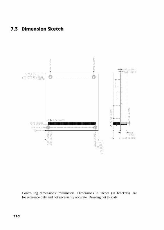
110
Dimension Sketch
Controlling dimensions: millimeters. Dimensions in inches (in brackets) arefor reference only and not necessarily accurate. Drawing not to scale.
7.3
111
Appendix A: TroubleshootingThe following notes might help you when encountering problems after theinstallation of the PCM-4330 single board computer or software. If you can not solve the problem after referring to this section, please contact yourdealer who will need the following information together with your problemreport:
n Description of the problem.n Have you tried workarounds? Which?n Serial number of your PCM-4330.n Type and model of your computer system.n Type and model of expansion cards installed in the system.n Name and version of installed software and drivers.n Error messages by POST, operating software or application software (if any)n Hardcopy of the files AUTOEXEC.BAT, CONFIG.SYS, SYSTEM.INI and WIN.INI (MS-DOS and MS-Windows only).
Problem It seems as if the system is performing system checks and booting fileoperating system but there is no output on the screen.
AnswerPlease check the following:
8 Is the PCM-4330PC/104 board computer installed properly?8 Check power supply of computer system and monitor. If the display has
its own power switch, make sure it is set to the on position.8 If an additional graphics adapter is installed in the system, remove the second-
ary adapter and check whether the system operates properly with only one graph-ics adapter installed.
8 Check settings of the switches and jumpers on the PCM-4330 board.8 Check settings of DIL-switches SW.3 to SW.8 of the LC display configuration
switches. Check the LCD connector and cabling between the display and thePCM-4330 board (proper connectors, polarity).

112
Problem(Graphics) application software does not display correctly on the CRT or LCDdisplay.
Answer8 Return to DOS and reboot the system and reload the operating software.8 Check the installation instructions of the application software; select a video
mode and resolution that is supported the monitor or LCD display.8 Restart the (graphics) application software.
ProblemAfter installation of a new display driver under MS-Windows the monitor orLC-display does not operate properly.
Answer8 Return to DOS and reboot the system.8 Change into the MS-Windows directory.8 Start the MS-Windows Setup-Program and select the standard VGA display
driver for your system.8 Quit the Setup-program.8 Install a display driver for the PCM-4330 board (see section 2.4.1 on page 35)
that uses a video mode and resolution that is supported by your monitor orLC-Display (see Appendix B: LC-Displays).
ProblemYou have selected a higher display resolution under MS-Windows using the West-ern Digital Display Changer. However, the display resolution is still unchanged.
Answer8 Please check the settings of the configuration switches.8 If you are using a CRT display only, make sure that switch SW.2 of the configu-
ration switches is set to on.8 If you are using a simultaneous display on a CRT and LC display, the settings of
switches SW.3 to SW.8 limit the maximum display resolution possible. Youcan not select a higher resolution than selected for the display.

113
Display BIOS-Code SW.3 SW.4 SW.5 SW.6 SW.7 SW.8
Mono Dual-Scan Display 8 Bit on on
reserved on on on
Color Dual-Scan Display 16 Bit on on on
Color Dual-Scan Display 16 Bit on on on on
reserved on on on
reserved on on on on
reserved on on on on
reserved on on on on on
reserved on
reserved on on
00
01
02
03
04
05
06
07
08
09
Appendix B: LC-DisplaysThe following section contains an excerpt of supported LC-displays withreference tables assigning individual pins of the universal LCD connector onthe PCM-4330 board to signal lines of several LC-displays and indicatingproper configuration switch settings.Please contact your PCM-4330 dealer if you cannot find your LC-display inthe following lists and ask for the LCD-Connector manual, which containsconstantly updated lists of all supported displays and further configuration detailsand notes.Configuration SwitchesA row of configuration switches (DIL-switches) on the PCM-4330 board isused to select the connected LC-display. The individual keys of the configu-ration switches are assigned the following function:
SW.1SW.2
SW.3SW.4SW.5SW.6SW.7SW.8
Please refer to figure 4 on page 14 for the location of these switches.
(reserved)Toggle between CRT and CRT/LCD simultaneous operationon: CRT onlyoff: CRT and LCD simultaneouslyPanel Technology 0Panel Technology 1Display Configuration 0Display Configuration 1Display Configuration 2Display Configuration 3
114
Display BIOS-Code SW.3 SW.4 SW.5 SW.6 SW.7 SW.8
reserved 0A on on
reserved 0B on on on
reserved 0C on on
reserved 0D on on on
reserved 0E on on on
reserved 0F on on on on
EL Display (Sharp) Pixel 10 on
EL Display 1 Pixel 11 on on
EL Display 2 Pixel 12 on on
Mono TFT Display 13 on on on
EL Display (640x400) 1 Pixel(no grayscale)
14 on on on
EL Display (640x400) 1 Pixel(no grayscale)
15 on on on on
reserved 16 on on on
reserved 17 on on on on
9 Bit Color TFT Display 18
9 Bit Color TFT Display 19 on
9 Bit Color TFT Display 1A on
9 Bit Color TFT Display 1B on on
Color Single-Scan Display 8 Bit 1C on
Color Single-Scan Display 8 Bit 1D on on
Color Single-Scan Display 8 Bit 1E on on
reserved 1F on on on
115
Monochrome Dual-Scan Displays
Display Display TypeConfiguration Switches
set to "on"
Max. Contrast
Voltage
Hosiden HLM8619MonochromeDual-Scan
3,4 -24 Volt (to GND)
Sanyo LCM-5494-24NTRMonochromeDual-Scan
3,4 -26 Volt (to GND)
Sanyo LMC-5505-32NTKMonochromeDual-Scan
3,4 (no data available)
Torisan LM-KE55-32NTKMonochromeDual-Scan
3,4 -24 Volt (to GND)
Sharp LM 64P10MonochromeDual-Scan
3,4 -24 Volt (to GND)
Sharp LM 64P89MonochromeDual-Scan
3,4 -22 Volt (to GND)
Sharp LM 64P831MonochromeDual-Scan
3,4 -22 Volt (to GND)
EL Displays
Display Display TypeConfiguration Switches
set to "on"
Max. Contrast
Voltage
Planar EL640.400-C21 Pixel no grayscale(640x400)
4,7,8no contrast voltagerequired
Planar EL640.400-CD31 Pixel no grayscale(640x400)
4,7,8no contrast voltagerequired
Planar EL640.400-CE11 Pixel no grayscale(640x480)
4,5,7,8no contrast voltagerequired
Planar EL640.480-A4 1 Pixel no grayscale 4,5no contrast voltagerequired
Planar EL640.480-AA1 1 Pixel no grayscale 4,5no contrast voltagerequired
Fujitsu FPF8050Hrud-0011 Pixel no grayscale(640x400)
4,6,7,8no contrast voltagerequired
Sharp LJ64ZU492 Pixel 16 grayscale(640x400)
4,8no contrast voltagerequired

116
Monochrome Dual-Scan Displays
Display Display TypeConfiguration Switches
set to "on"
Max. Contrast
Voltage
Sharp LM64P839MonochromeDual-Scan
3,4 -22 Volt (to GND)
Hitachi LMG5160XUFC-3MonochromeDual-Scan
3,4 -22 Volt (to GND)
Hitachi LMG5161XUFC-CMonochromeDual-Scan
3,4 -21 Volt (to GND)
Hitachi LMG5168XUFC-CMonochromeDual-Scan
3,4 -21 Volt (to GND)
Hitachi LMG6911RPBCMonochromeDual-Scan
3,4 -22 Volt (to GND)
Color Dual-Scan Displays
Display Display TypeConfiguration Switches
set to "on"
Max. Contrast
Voltage
Hosiden HLM6678-015211 Color Dual-Scan 1 3,4,6 35 Volt (to GND)
Kyocera KCS6448CSTT Color Dual-Scan 1 3,4,6 36 Volt (to GND)
Sanyo LCM-5331-22NTK Color Dual-Scan 1 3,4,6 30 Volt (to GND)
Sanyo LCM-5334-22NTK Color Dual-Scan 1 3,4,6 28 Volt (to GND)
Sanyo LCM-CC53-22NTK Color Dual-Scan 1 3,4,6 30 Volt (to GND)
Torisan LM-CA53-22NTK Color Dual-Scan 1 3,4,6 30 Volt (to GND)
Torisan LM-CD53-22NTK Color Dual-Scan 1 3,4,6 28 Volt (to GND)
Torisan LM-CF53-22NTK Color Dual-Scan 1 3,4,6 30 Volt (to GND)
Torisan LM-DC53-22NTK Color Dual-Scan 1 3,4,6 28 Volt (to GND)
Torisan LM-HB53-22NTK Color Dual-Scan 1 3,4,6 -24 Volt (to GND)
Sharp LM64C08P Color Dual-Scan 1 3,4,6 32.6 Volt (to GND)
Sharp LM64C35P Color Dual-Scan 1 3,4,6 25.5 Volt (to GND)
Sharp LM64C152 Color Dual-Scan 1 3,4,6 25.5 Volt (to GND)
Hitachi LMG9460XUCC Color Dual-Scan 1 3,4,6 6 Volt (to GND)
Hitachi LMG9520RPCC Color Dual-Scan 1 3,4,6 23 Volt (to GND)
Hitachi LMG9822XUCC-A1 Color Dual-Scan 1 3,4,6 32 Volt (to GND)
Orion OEM-6448C-2 Color Dual-Scan 1 3,4,6 35 Volt (to GND)
117
TFT Color Displays
Display Display TypeConfiguration Switches
set to "on"
Max. Contrast
Voltage
Seiko Epson EG9013F-NZMonochromeSingle-Scan 1
6,7 35 Volt (to GND)
TFT Color Displays
Display Display TypeConfiguration Switches
set to "on"
Max. Contrast
Voltage
Toshiba LTM09C016K 9 Bit Color TFT (all switches set to "off")no contrast voltagerequired
Toshiba LTM10C015K 9 Bit Color TFT (all switches set to "off")no contrast voltagerequired
Toshiba LTM10C025K 18 Bit Color TFT 5,6no contrast voltagerequired
Toshiba LTM10C040K 18 Bit Color TFT 5,6no contrast voltagerequired
Toshiba LTM10C042 18 Bit Color TFT 5,6no contrast voltagerequired
Toshiba LTM10C209(A) 18 Bit Color TFT 5,6no contrast voltagerequired
Sharp LQ9D011 9 Bit Color TFT (all switches set to "off")no contrast voltagerequired
Sharp LQ10D011 9 Bit Color TFT (all switches set to "off")no contrast voltagerequired
Sharp LQ10D11 9 Bit Color TFT (all switches set to "off")no contrast voltagerequired
Sharp LQ10D15 9 Bit Color TFT (all switches set to "off")no contrast voltagerequired
Sharp LQ10D021 9 Bit Color TFT 5,6no contrast voltagerequired
Sharp LQ14D311 18 Bit Color TFT 5,6no contrast voltagerequired
Sharp LQ10D131 12 Bit Color TFT 6no contrast voltagerequired
Sharp LQ64D131 12 Bit Color TFT 6no contrast voltagerequired
Sharp LQ10D321 18 Bit Color TFT 5,6no contrast voltagerequired
NEC NL6448AC20-10 12 Bit Color TFT 6no contrast voltagerequired
NEC NL6448AC20-02 12 Bit Color TFT 6no contrast voltagerequired
118
TFT Color Displays
Display Display TypeConfiguration Switches
set to "on"
Max. Contrast
Voltage
NEC NL6448AC30-06 12 Bit Color TFT 6no contrast voltagerequired
NEC NL6448AC30-10 12 Bit Color TFT 6no contrast voltagerequired
NEC NL6448AC32-01 18 Bit Color TFT 5,6no contrast voltagerequired
NEC NL6448AC33-10 12 Bit Color TFT 6no contrast voltagerequired
NEC NL6448AC30-15 12 Bit Color TFT 6no contrast voltagerequired
NEC NL8060AC24-01special setting:(800x600)18 Bit-TFT
6,7no contrast voltagerequired
NEC NL8060AC26-02special setting:(800x600)18 Bit-TFT
6,7no contrast voltagerequired
Hitachi TX26D60VC1CAB 18 Bit Color TFT 5,6no contrast voltagerequired
TFD Color Displays
Display Display TypeConfiguration Switches
set to "on"
Max. Contrast
Voltage
FPD LDH102T-10 18 Bit Color TFD 5no contrast voltagerequired
FPD LDH102T-20 18 Bit Color TFD 5no contrast voltagerequired
LCD-Enable-SignalThe LCD-Enable-Signal (Panel Off Signal) is used to control the LC-displaysand can be set to low or high. Use the appropriate jumper to select the polarity ofthis signal.
CablingThe following tables contain pin assignments for a range of standard LC-displays to the pins of the universal LCD connector on the PCM-4330 board.If you can not find a suitable display type in one of the tables and the examplesare insufficient to produce a custom cable, please contact your PCM-4330 dealer.
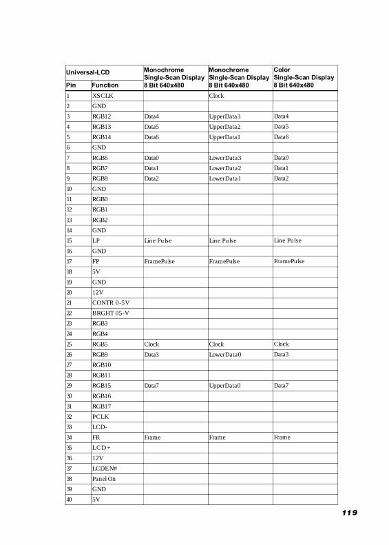
119
Universal-LCD Monochrome
Single-Scan Display
8 Bit 640x480
Monochrome
Single-Scan Display
8 Bit 640x480
Color
Single-Scan Display
8 Bit 640x480Pin Function
1 XSCLK Clock
2 GND
3 RGB12 Data4 UpperData3 Data4
4 RGB13 Data5 UpperData2 Data5
5 RGB14 Data6 UpperData1 Data6
6 GND
7 RGB6 Data0 LowerData3 Data0
8 RGB7 Data1 LowerData2 Data1
9 RGB8 Data2 LowerData1 Data2
10 GND
11 RGB0
12 RGB1
13 RGB2
14 GND
15 LP Line Pulse Line Pulse Line Pulse
16 GND
17 FP FramePulse FramePulse FramePulse
18 5V
19 GND
20 12V
21 CONTR 0-5V
22 BRGHT 05-V
23 RGB3
24 RGB4
25 RGB5 Clock Clock Clock
26 RGB9 Data3 LowerData0 Data3
27 RGB10
28 RGB11
29 RGB15 Data7 UpperData0 Data7
30 RGB16
31 RGB17
32 PCLK
33 LCD-
34 FR Frame Frame Frame
35 LCD+
36 12V
37 LCDEN#
38 Panel On
39 GND
40 5V
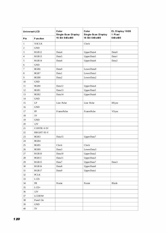
120
Universal-LCD Color
Single-Scan Display
16 Bit 640x480
Color
Single-Scan Display
16 Bit 640x480
EL D isplay 16GS
1 Pixel
640x480Pin Function
1 XSCLK Clock
2 GND
3 RGB12 Data4 UpperData4 Data0
4 RGB13 Data5 UpperData5 Data1
5 RGB14 Data6 UpperData6 Data2
6 GND
7 RGB6 Data0 LowerData0
8 RGB7 Data1 LowerData1
9 RGB8 Data2 LowerData2
10 GND
11 RGB0 Data12 UpperData4
12 RGB1 Data13 UpperData5
13 RGB2 Data14 UpperData6
14 GND
15 LP Line Pulse Line Pulse HSync
16 GND
17 FP FramePulse FramePulse VSync
18 5V
19 GND
20 12V
21 CONTR 0-5V
22 BRGHT 05-V
23 RGB3 Data15 UpperData7
24 RGB4
25 RGB5 Clock Clock
26 RGB9 Data3 LowerData3
27 RGB10 Data10 UpperData2
28 RGB11 Data11 UpperData3
29 RGB15 Data7 UpperData7 Data3
30 RGB16 Data8 UpperData0
31 RGB17 Data9 UpperData1
32 PCLK
33 LCD-
34 FR Frame Frame Blank
35 LCD+
36 12V
37 LCDEN#
38 Panel On
39 GND
40 5V

121
Universal-LCD EL D isplay 16GS
2 Pixel
640x480
EL D isplay 16GS
1 Pixel
640x480
EL D isplay 16GS
1 Pixel
640x480Pin Function
1 XSCLK Clock Clock Clock
2 GND
3 RGB12 Data0 Data0 Data0
4 RGB13 Data1 Data1
5 RGB14 Data2 Data2
6 GND
7 RGB6 Data0
8 RGB7 Data1
9 RGB8 Data2
10 GND
11 RGB0
12 RGB1
13 RGB2
14 GND
15 LP HSync HSync HSync
16 GND
17 FP VSync VSync VSync
18 5V
19 GND
20 12V
21 CONTR 0-5V
22 BRGHT 05-V
23 RGB3
24 RGB4
25 RGB5
26 RGB9 Data13
27 RGB10
28 RGB11
29 RGB15 Data03 Data3
30 RGB16
31 RGB17
32 PCLK
33 LCD-
34 FR Blank Blank Blank
35 LCD+
36 12V
37 LCDEN#
38 Panel On
39 GND
40 5V
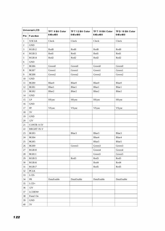
122
Universal-LCDTFT 9 Bit Color
640x480
TF T 12 Bit Color
640x480
TF T 18 Bit Color
640x480
TF D 18 Bit Color
640x480Pin Function
1 XSCLK Clock Clock Clock Clock
2 GND
3 RGB12 Red0 Red0 Red0 Red0
4 RGB13 Red1 Red1 Red1 Red1
5 RGB14 Red2 Red2 Red2 Red2
6 GND
7 RGB6 Green0 Green0 Green0 Green0
8 RGB7 Green1 Green1 Green1 Green1
9 RGB8 Green2 Green2 Green2 Green2
10 GND
11 RGB0 Blue0 Blue0 Blue0 Blue0
12 RGB1 Blue1 Blue1 Blue1 Blue1
13 RGB2 Blue2 Blue2 Blue2 Blue2
14 GND
15 LP HSync HSync HSync HSync
16 GND
17 FP VSync VSync VSync VSync
18 5V
19 GND
20 12V
21 CONTR 0-5V
22 BRGHT 05-V
23 RGB3 Blue3 Blue3 Blue3
24 RGB4 Blue4 Blue4
25 RGB5 Blue5 Blue5
26 RGB9 Green3 Green3 Green3
27 RGB10 Green4 Green4
28 RGB11 Green5 Green5
29 RGB15 Red3 Red3 Red3
30 RGB16 Red4 Red4
31 RGB17 Red5 Red5
32 PCLK
33 LCD-
34 FR DataEnable DataEnable DataEnable DataEnable
35 LCD+
36 12V
37 LCDEN#
38 Panel On
39 GND
40 5V

123
Do not cancel the program with a reset. This might otherwise render the computer inoperative since the 8105 may be deleted.
Appendix C: Silicon DiskTo use the on-board flash module on the PCM-4330 board to emulate a harddisk drive (silicon disk) follow these steps:
BlOS-Requirements and CMOS-Settingsn The BIOS version on the PCM-4330 board must be 1.0c or higher to support the
memory module.n To emulate a silicon disk, the 8105 extension requires that the memory area
in which the extension is started is available as Shadow-RAM.n The ROM extension is started in area CC00 — CFFF. Therefore, this segment
must be set to Shadow RAM in the setup menu (see page 23).n The emulation uses area D0000— D3FFF as a window to the memory module.
Consequently, no other program or driver may use this area. Additionally,Shadow-RAM needs to be disabled for this segment.
n To disable loading the 8105 extension, simply set the CMOS-RAM date tothe year 2099. If the year is set to 2098, only a part of the extension is loaded.The modifications for INT 13 will not be loaded.
BIOS Extension SetupTo set up the 8105 extension, enter the following command at a DOS prompt:flashcl -v = FlashBIOS.<ver><ver> indicates the current version of the 8105 extension.
Low Level FormattingBefore using the silicon disk it must first be initialized with the memcform pro-gram. A signature and further parameters enable the 8105 extension toidentify and access the disk. A drive number needs to be assigned to the diskbefore the formatting process:n Select values “0” to “9” for drive numbers 0x80 to 0x89 or values “A” to “F”
for drive numbers 0xFA to 0xFF.n If a drive number is selected which is smaller or equal to a number of an ex-
isting hard disk drive, the number of the hard disk drive is raised for INT 53.n Choose any drive number if no hard disk drive is installed in the system.n If value “0” (corresponding to drive number 0x80) is selected for the silicon
disk in a system with a hard disk drive, drive letter C: is assigned to the silicondisk and letter D: to the hard disk. Value “F” swaps drive letter assignments(letter C: for the hard disk drive and letter D: for the silicon disk).
124
Enter the following command at a DOS prompt to start low level formatting:memcform <paraml><param2>
Enter “S” for param1 to format a SRAM-Module or “F” for a Flash-Memory.Entering “Z” for param2 will start the formatting without any further user input(if possible).After low level formatting the computer must be rebooted for the changes totake effect.
GetMem Device DriverThe BIOS extension requires the getmem driver which provides BIOS expansionmemory (about 600 bytes). Add the following line to your config.sys file:
device=getmem.exe
DOS FormattingThe silicon disk can now be prepared for use with the fdisk and format DOSprograms. If a hard disk drive is installed in the system, make sure that fdisk ispointing to the appropriate disk (option “5”). The silicon disk is not entered into the CMOS-RAM. No additionalcontroller(such as an IDE-Controller) is required to use the silicon disk.
ReorganizationIf the silicon disk is predominately used for read operations, access times can pos-sibly (depending on the disk size) be improved by reorganizing sector ordering.Use the memcform program to start the reorganization process:memcform rs
Do not use any other method but the ESC key to stop arunning reorganization process. CTRL- C or a system reset mayresult in data loss.After stopping the reorganization using the ESC key, the cur-rent segment and possibly one more segment are processed be-fore the program stops. This might take up to 2 seconds. Theprogram can then be restarted to resume the reorganization.
Additional ConsiderationsThe segment D0000 — D3FFFF is used by the BIOS extension as a window to thememory module. Therefore this segment needs to be protected from accesses by anyother program. This segment range should therefore be excluded when installing amemory manager such as emm386.

125
Installing PC/104 modulesThe CPU card's PC/104 connectors give you the flexibility toattach PC/104 expansion modules. These modules perform thefunctions of traditional plug-in expansion cards, but save spaceand valuable slots. Modules include:
• PCM-4330 486 CPU Module with Flat Panel/CRT Interface• PCM-3335 386 CPU Module w/ Flat Panel/CRT Interface• PCM-3600 FAX/Modem Module• PCM-3420 Fast SCSI-2 Module• PCM-3200 Sound Module• PCM-3810 Solid State Disk Module• PCM-3820 High Density Flash Disk Module• PCM-3115 PCMCIA Module (two slots)• PCM-3610 Isolated RS-232 and RS-422/485 Module• PCM-3660 Ethernet Module• PCM-3718 30 KHz A/D Module• PCM-3724 48-Channel DIO Module• PCM-3910 Breadboard ModuleInstalling these modules on the CPU card is quick and simple. Thefollowing steps show how to mount the PC/104 modules:
1. Remove the CPU card from your system paying particularattention to the safety instructions already mentioned.
2. Make any jumper or link changes required to the CPU cardnow. Once the PC/104 module is mounted you may havedifficulty in accessing these.
3. Normal PC/104 modules have male connectors and mountdirectly onto the main card. However, to ensure better busmatching, the connectors on the CPU card and the PC/104module are both female. For this reason, you may need to usethe "male-male" adapter included with the CPU card in orderto properly connect your PC/104 module. (Refer to the diagramon the following page.)
4. Mount the PC/104 module onto the CPU card by pressing themodule firmly but carefully onto the mounting connectors.
5. Secure the PC/104 module onto the CPU card using the fourmounting spacers and srews.
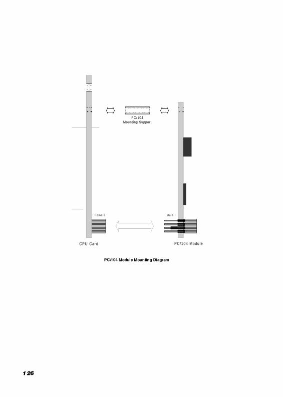
126
PC/104 ModuleCPU Card
PC/104Mount ing Support
Fema le Ma le
PC/104 Module Mounting Diagram

127