pci device configuration: bars &...
TRANSCRIPT

PC Chipset: Functions & Devices Ch-2
Intel Architecture Technical Training Page 1
PC Chipset: Functions & Devices
PCI Device PCI Device Configuration:Configuration:
BARs & Interrupts BARs & Interrupts Chapter 2Chapter 2
Copyright Copyright ©© 19961996--2003 Intel Corp.2003 Intel Corp.
CH-2 Slide-2PC Chipset: Functions & Devices
PCI Device ConfigurationOBJECTIVES: Upon completion of this topic, the
participant will be able to do the following:Recognize ® Windows ® Device Manager displays. Discuss the functions of the PCI Command registerDescribe memory space allocation using BARsExplain the use of PCI Interrupt Pin/Line Configuration Registers
IATT Web Site: http://iatt.intel.com
PC Chipset: Functions & Devices Ch-2
Intel Architecture Technical Training Page 2
CH-2 Slide-3PC Chipset: Functions & Devices
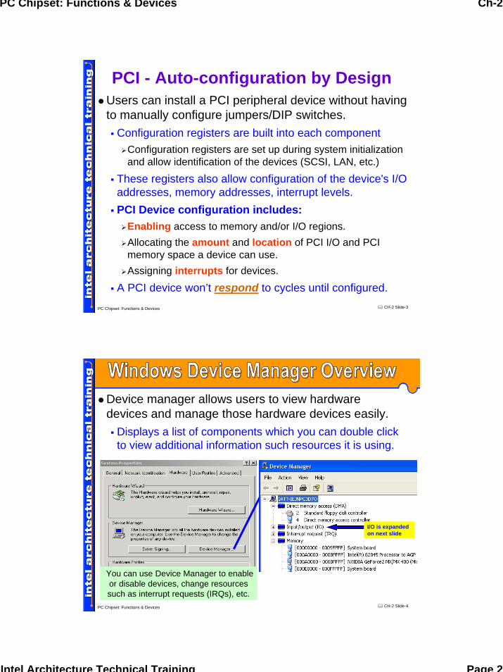
PCI - Auto-configuration by DesignUsers can install a PCI peripheral device without having to manually configure jumpers/DIP switches.
Configuration registers are built into each component Configuration registers are set up during system initialization and allow identification of the devices (SCSI, LAN, etc.)
These registers also allow configuration of the device's I/O addresses, memory addresses, interrupt levels.PCI Device configuration includes:
Enabling access to memory and/or I/O regions.Allocating the amount and location of PCI I/O and PCI memory space a device can use.Assigning interrupts for devices.
A PCI device won’t respond to cycles until configured.
CH-2 Slide-4PC Chipset: Functions & Devices
Device manager allows users to view hardware devices and manage those hardware devices easily.
Displays a list of components which you can double click to view additional information such resources it is using.
You can use Device Manager to enable or disable devices, change resources such as interrupt requests (IRQs), etc.
I/O is expanded on next slide
PC Chipset: Functions & Devices Ch-2
Intel Architecture Technical Training Page 3
CH-2 Slide-5PC Chipset: Functions & Devices
Portion of Windows DEV MGR I/O Map
Note: One I/O address associated with the AC97 device is “E800”. The allocation of Memory & I/O
addresses are described later in this chapter.
AC97 I/O = E800
See Appendix for more Information
CH-2 Slide-6PC Chipset: Functions & Devices
Device ID Vendor ID
Status Command
Class Code RevisionID
00h
04h
08h
016 1531Format of a PCI Configuration Header
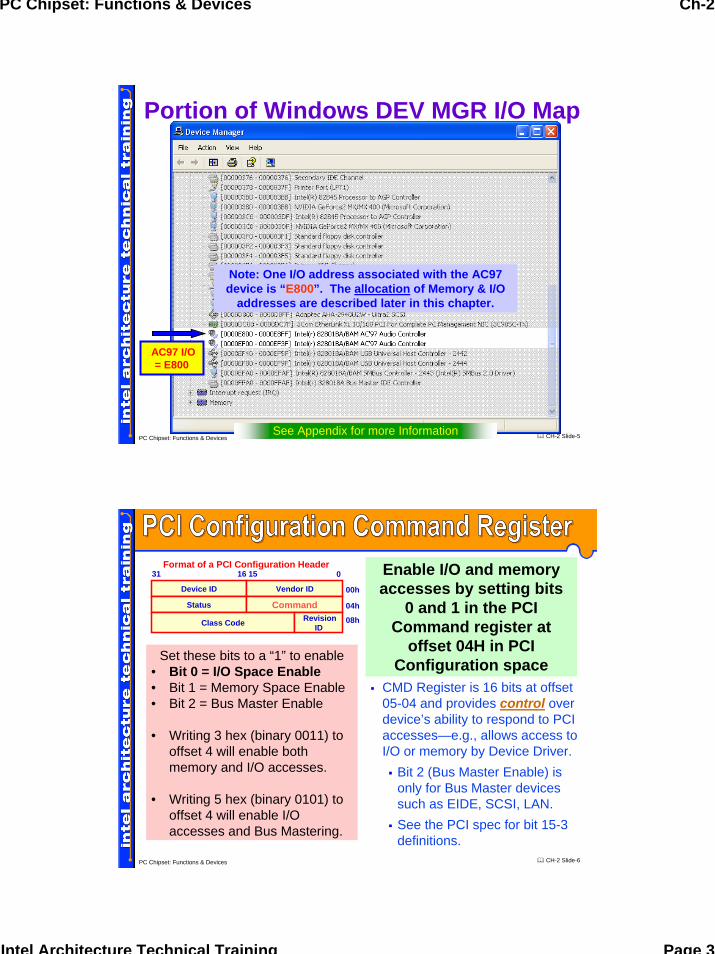
CMD Register is 16 bits at offset 05-04 and provides control over device’s ability to respond to PCI accesses—e.g., allows access to I/O or memory by Device Driver.
Bit 2 (Bus Master Enable) is only for Bus Master devices such as EIDE, SCSI, LAN.See the PCI spec for bit 15-3 definitions.
Enable I/O and memory accesses by setting bits
0 and 1 in the PCI Command register at
offset 04H in PCI Configuration space Set these bits to a “1” to enable
• Bit 0 = I/O Space Enable • Bit 1 = Memory Space Enable• Bit 2 = Bus Master Enable
• Writing 3 hex (binary 0011) to offset 4 will enable both memory and I/O accesses.
• Writing 5 hex (binary 0101) to offset 4 will enable I/O accesses and Bus Mastering.

PC Chipset: Functions & Devices Ch-2
Intel Architecture Technical Training Page 4
CH-2 Slide-7PC Chipset: Functions & Devices
Making Changes to CMD Regs ( 1 of 2)The dump below of AC97 PCI configuration space shows offset 4 contains a hex “05” or binary “0101”. This means bits 2 and 0 are both set—I/O & Bus Mstr are both enabled.
[P0]>showpci (0,1f,5) /* Device 31, Fun 5-–AC97 ctlr */
Offset F E D C B A 9 8 7 6 5 4 3 2 1 0
--------------------------------------------
0F...00: 00000000 04010005 02800005 24458086
Note: The I/O address associated with the AC97 device is “E800”.
The allocation of Memory & I/O addresses are described later in this chapter.
ICH AC97 Mixer RegisterOffset 2 is Vol/Mute (Addr E802)
MSB is Mute: 8000 = MuteOther bits are Left/Rt vol.
Example values are:8000 = Mute0000 = Full Volume0505 = Mid Range8505 = Mute & Mid Vol3f3f = Min Volume
16 bit regs
ICH AC97 Mixer Register (part of)
CH-2 Slide-8PC Chipset: Functions & Devices
Making Changes to CMD Regs ( 2 of 2)The ITP Debug Tool commands below show what happens when I/O access is enabled/disabled by setting/clearing bits in the command register--offset 04h.
[P0]>dport (0cf8)=8000fd04;port (0cfc)
05 /* This reads 05 from AC97 cmd reg (bus mstr & I/O enabled) */
[P0]>wport (0e802) /* AC97 I/O range E800-E8FF */
8505 /* Able to read 8505 (mute & Mid Vol) from I/O addr E802 */
[P0]>/* Now change cmd reg to 00: bus mstr & I/O disabled */
[P0]>dport (0cf8)=8000fd04;port (0cfc)=00
[P0]>wport (0e802)
ffff /* No longer able to read data from I/O address E802 */
[P0]>dport (0cf8)=8000fd04;port (0cfc)=05
[P0]>/* Change cmd reg back to 05 = bus mstr & I/o enabled again */
[P0]>wport (0e802)
8505 /* Again able to read data of “8505” from I/O addr E802 */
PC Chipset: Functions & Devices Ch-2
Intel Architecture Technical Training Page 5
CH-2 Slide-9PC Chipset: Functions & Devices
The Command Register in PCI Configuration space is 16 bits starting at offset 04 and allows control of ______ and I/O space enable/disable.
Memory
M-1M-1
CH-2 Slide-10PC Chipset: Functions & Devices
Device ID Vendor ID
Status Command
Class Code RevisionID
BIST HeaderType
LatencyTimer
Cache LineSize
Base Address Registers(32 bits each at offsets 10h-27h)
Reserved
Reserved
Expansion ROM Base Address
Reserved
Reserved
Max_Lat Min_Gnt InterruptPin
Interrupt Line
00h
04h
08h
0Ch
10h
14h
18h
1Ch
20h
24h
28h
2Ch
30h
34h
38h
3Ch
016 1531
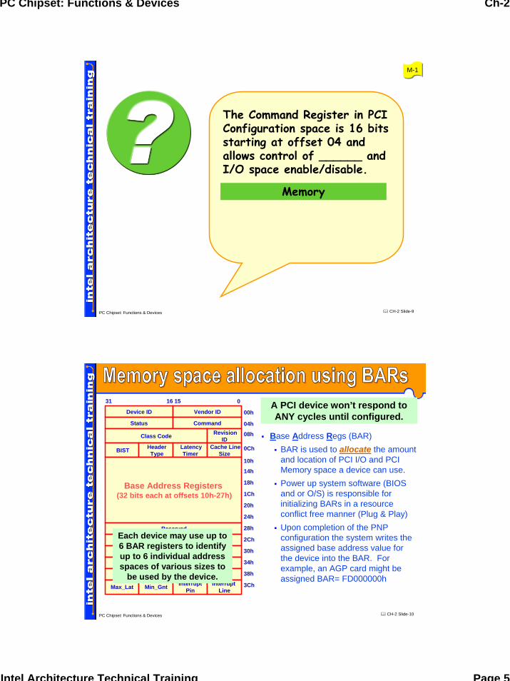
Base Address Regs (BAR) BAR is used to allocate the amount and location of PCI I/O and PCI Memory space a device can use. Power up system software (BIOS and or O/S) is responsible for initializing BARs in a resource conflict free manner (Plug & Play)Upon completion of the PNP configuration the system writes the assigned base address value for the device into the BAR. For example, an AGP card might be assigned BAR= FD000000h
A PCI device won’t respond to ANY cycles until configured.
Each device may use up to 6 BAR registers to identify up to 6 individual address spaces of various sizes to
be used by the device.

PC Chipset: Functions & Devices Ch-2
Intel Architecture Technical Training Page 6
CH-2 Slide-11PC Chipset: Functions & Devices
Base Address Registers (BAR)Upon power-up, the BAR identifies the resources required by the device. BIOS and other software writes all 1’s and reads value back to determine size and alignment (see PCI spec for details)System software uses these addresses to access device.
0 for memory space1 for I/O space
Base Address
31 0
Bottom bit of Base Address Reg specifies which address space.
The remainder of the bits identify how much space is required.
BAR USE:Request memory and/or I/O space.
BARs provide the mechanism for mapping PCI devices into the
system address space.
PCI devices do not need to utilize all of the BAR regions available.
A BAR value of zero indicates that the device has not requested that any system resources.
CH-2 Slide-12PC Chipset: Functions & Devices
Example Memory Map - After configuration
PCI Device A
Bridge.PCI Bus
PCI Device B PCI Device C
BAR =2 GB
BAR =3 GB
BAR =1 GB
System Memory Space
640KB 1MB 4GB0 3GBDev C
2GBDev B
1GBDev A
Top of Memory(256 MB for example) Physical memory (i.e., SDRAM)
does not exist above T.O.M.

PC Chipset: Functions & Devices Ch-2
Intel Architecture Technical Training Page 7
CH-2 Slide-13PC Chipset: Functions & Devices
Windows Device MGR I/O Map
After Configuration: AC97 was assigned I/O space
starting at 0000E800 & 0000EF00
AC97 E800
CH-2 Slide-14PC Chipset: Functions & Devices
Windows Device MGR Memory Map
AGP F8000000
AGP A00000
After Configuration: AGP was assigned memory space starting at F8000000 &
FC900000 & FD000000 (as well as the standard VGA Video Buffer at 000A0000--reserved mem area below Top of Memory)

PC Chipset: Functions & Devices Ch-2
Intel Architecture Technical Training Page 8
CH-2 Slide-15PC Chipset: Functions & Devices
PCI Dev# 0 [ 0h]: Fun# 0 DID/VID = 1a308086 [dport(0cf8)=8000003c]
BAR-10=f8000008, BAR-14=00000000 /* Mem Ctlr */
PCI Dev# 1 [ 1h]: Fun# 0 DID/VID = 1a318086 [dport(0cf8)=8000083c]
BAR-10=00000000, BAR-14=00000000 /* AGP Bridge */
PCI Dev# 31 [1Fh]: Fun# 4 DID/VID = 24448086 [dport(0cf8)=8000fc3c]
BAR-10=00000000, BAR-14=00000000 /* USB #2 */
PCI Dev# 31 [1Fh]: Fun# 5 DID/VID = 24458086 [dport(0cf8)=8000fd3c]
BAR-10=0000e801, BAR-14=0000ef01 /* AC97 */
Now dumping PCI bus 1.
PCI Dev# 0 [ 0h]: Fun# 0 DID/VID = 011010de [dport(0cf8)=8001003c]
BAR-10=fd000000, BAR-14=e8000008 /* AGP card */
Now dumping PCI bus 2.
PCI Dev# 10 [ Ah]: Fun# 0 DID/VID = 00109005 [dport(0cf8)=8002503c]
BAR-10=0000d801, BAR-14=feaff004 /* SCSI card */
PCI Dev# 11 [ Bh]: Fun# 0 DID/VID = 920010b7 [dport(0cf8)=8002583c]
BAR-10=0000dc01, BAR-14=feafec00 /* LAN card */
ITP Dump of BARs After Configuration
••• Note: Partial list – not all devices shown
Compare this to Device MGR display on previous slides
PCI Dev# 0 [ 0h]: Fun# 0 DID/VID = 1a308086 [dport(0cf8)=8000003c]
BAR-10=f8000008, BAR-14=00000000 /* Mem Ctlr */
PCI Dev# 1 [ 1h]: Fun# 0 DID/VID = 1a318086 [dport(0cf8)=8000083c]
BAR-10=00000000, BAR-14=00000000 /* AGP Bridge */
PCI Dev# 31 [1Fh]: Fun# 4 DID/VID = 24448086 [dport(0cf8)=8000fc3c]
BAR-10=00000000, BAR-14=00000000 /* USB #2 */
PCI Dev# 31 [1Fh]: Fun# 5 DID/VID = 24458086 [dport(0cf8)=8000fd3c]
BAR-10=0000e801, BAR-14=0000ef01 /* AC97 */
Now dumping PCI bus 1.
PCI Dev# 0 [ 0h]: Fun# 0 DID/VID = 011010de [dport(0cf8)=8001003c]
BAR-10=fd000000, BAR-14=e8000008 /* AGP card */
Now dumping PCI bus 2.
PCI Dev# 10 [ Ah]: Fun# 0 DID/VID = 00109005 [dport(0cf8)=8002503c]
BAR-10=0000d801, BAR-14=feaff004 /* SCSI card */
PCI Dev# 11 [ Bh]: Fun# 0 DID/VID = 920010b7 [dport(0cf8)=8002583c]
BAR-10=0000dc01, BAR-14=feafec00 /* LAN card */
CH-2 Slide-16PC Chipset: Functions & Devices
Effects of writing to AGP MemoryPortion of Windows desktop. The digital data representing this screen is stored in AGP video memory at A0000 and System memory at E8000000.0x00000000000a0000P efbeefbe ef9eef9e ef9eef9e ef9eef9e
0x00000000000a0010P f79ef79e f7def7bf f7def7be f7bef7be
0x00000000000a0020P f79ef79e f7bef7be f7bff7bf ef9ef79f
0x00000000e8000000P efbeefbe ef9eef9e ef9eef9e ef9eef9e
0x00000000e8000010P f79ef79e f7def7bf f7def7be f7bef7be
0x00000000e8000020P f79ef79e f7bef7be f7bff7bf ef9ef79f
Desktop after writing to AGP video memory at A0000.0x00000000000a0000P f0f0f0f0 f0f0f0f0 f0f0f0f0 f0f0f0f0
0x00000000000a0010P f0f0f0f0 f0f0f0f0 f0f0f0f0 f0f0f0f0
0x00000000000a0020P f0f0f0f0 f0f0f0f0 f0f0f0f0 f0f0f0f0
“f0f0f0f0” changes part of screen to a red color
Desktop after writing to System memory at E8000000.0x00000000e8000000P 33223322 33223322 33223322 33223322
0x00000000e8000010P 33223322 33223322 33223322 33223322
0x00000000e8000020P 33223322 33223322 33223322 33223322
0x00000000e8000030P 33223322 33223322 33223322 33223322
“33223322” changes part of red screen to a green colorNote: Red & Green shades not visible in Grayscale handout
PC Chipset: Functions & Devices Ch-2
Intel Architecture Technical Training Page 9
CH-2 Slide-17PC Chipset: Functions & Devices
The bottom bit of the Base Address Register specifies:
1: Max size of the BAR register
2: Config complete/not done
3: Memory or I/O Space
4: Amount of space required
3: Memory or I/O Space
M-1M-1
CH-2 Slide-18PC Chipset: Functions & Devices
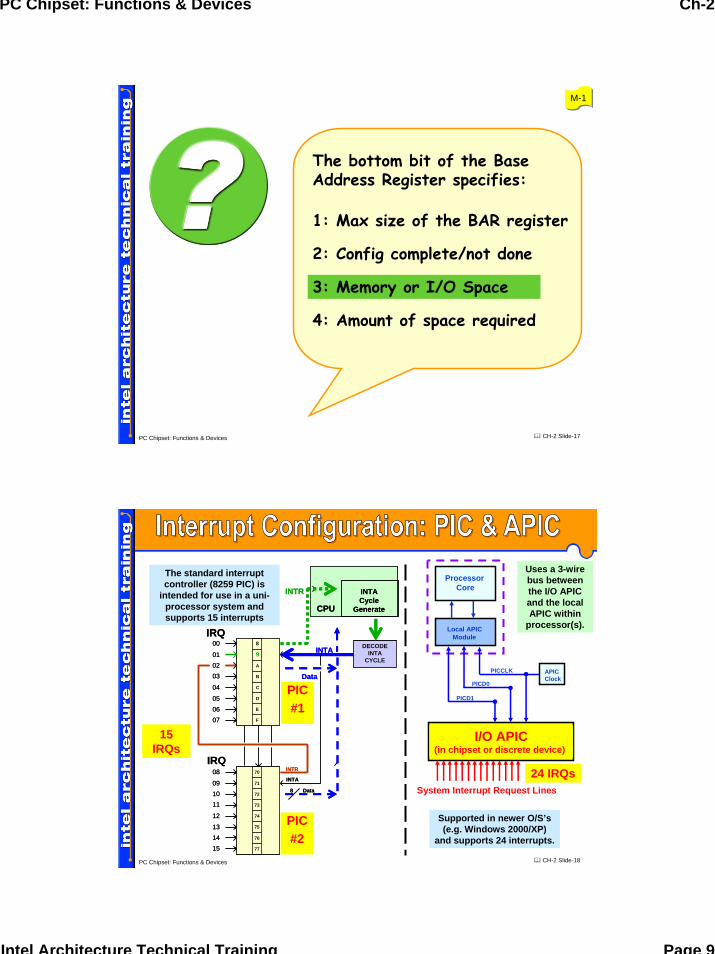
Supported in newer O/S’s (e.g. Windows 2000/XP)
and supports 24 interrupts.
15 IRQs
DECODEINTA
CYCLE
CPU
PIC#1
00
010203
04
050607
INTR
8 Data
INTA
8
9
A
B
C
D
E
F
70
71
72
73
74
75
76
77
INTR08
091011
12
131415
Data
IRQ
INTACycle
Generate
INTA
PIC#2
IRQ
DECODEINTA
CYCLE
CPU
PIC#1
00
010203
04
050607
INTR
8 Data
INTA
8
9
A
B
C
D
E
F
70
71
72
73
74
75
76
77
INTR08
091011
12
131415
Data
IRQ
INTACycle
Generate
INTA
PIC#2
IRQ
The standard interrupt controller (8259 PIC) is
intended for use in a uni-processor system and supports 15 interrupts
Processor Core
Local APICModule
PICD1
PICD0
PICCLK APIC Clock
I/O APIC (in chipset or discrete device)
System Interrupt Request Lines
Uses a 3-wire bus between the I/O APIC and the local APIC within
processor(s).
24 IRQs

PC Chipset: Functions & Devices Ch-2
Intel Architecture Technical Training Page 10
CH-2 Slide-19PC Chipset: Functions & Devices
PCI Hardware InterruptsMultiple PCI devices can be assigned to same IRQ.
The operating system calls each interrupt handler until one of the handlers claims the interrupt.
A typical chipset has 8 PIRQ input signals: PIRQ[H:A]# PCI connector interrupts signals (INTA, B, C, D) will connect to 1 of 8 ICH interrupt inputs (PIRQA#-PIRQH#).
Any PCI interrupt source (onboard or from a PCI add-in card) connects to one of these PIRQ signals.
In APIC mode, PIRQA#-PIRQH# are often routed to PCI interrupts IRQ16-IRQ23 respectively.
In PIC mode (legacy interrupts), the ICH can connect each PIRQ line internally to one of the IRQ signals (3-7, 9-12, 14, & 15)--each PIRQx# line has a separate Route Control register (e.g.,D31:F0 offsets 60h-6Bh for PIRQA#-PIRQH#
CH-2 Slide-20PC Chipset: Functions & Devices
PCI Configuration Registers--InterruptsRegister Number
Selects register within a particular Bus, Device, & Function (e.g., offset 3C or 3D)
016 1531
Device ID (02-03) Vendor ID (00-01)
Status Command
Class Code RevisionID
BIST HeaderType
LatencyTimer
Cache LineSize
Base Address Registers
Reserved
Reserved
Expansion ROM Base Address
Reserved
Reserved
Max_Lat Min_Gnt InterruptPin (3D)
Interrupt Line (3C)
00h
04h
08h
0Ch
10h
14h
18h
1Ch
20h
24h
28h
2Ch
30h
34h
38h
3Ch
3C3F 3E 3D
Interrupt Pin & Line use example:Pin (3D): 01 for INTA; 02 for INTB Line (3C): 10h -> IRQ16, 11h -> IRQ17
More details in next slides
Each PCI slot has 4 pins: INTA#, INTB#, INTC#, INTD#INTA is used for all add-in cards that require only 1 IRQINTB for the 2nd interrupt on cards that require 2 or more INTC & INTD: 3rd & 4th (not absolute requirements)
The interrupt line (IRQ) is read by software (O/S &
drivers) from the Interrupt Line register (offset 3C) in
the PCI Configuration Space of a device (3C
holds hex value of IRQ).

PC Chipset: Functions & Devices Ch-2
Intel Architecture Technical Training Page 11
CH-2 Slide-21PC Chipset: Functions & Devices
Each PCI slot has 4 pins: INTA#, INTB#, INTC#, and INTD#.
True
or
False
True
M-1M-1
CH-2 Slide-22PC Chipset: Functions & Devices
Typical Interrupt Routing (from TPS)
Chipset
ICH
(APIC mode)
PIRQA# [IRQ16]
PIRQB# [IRQ17]PIRQC# [IRQ18]PIRQD# [IRQ19]PIRQE# [IRQ20]PIRQF# [IRQ21]PIRQG# [IRQ22]
PIRQH# [IRQ23]
Input pins to chipset (ICH)
PIRQ[A :H]#
A typical chipset has 8 PIRQ input signals. PIRQ[H:A]# Each PCI slot has 4 pins: INTA#, INTB#, INTC#, INTD# INTA is used for all add-in cards that require only 1 IRQ
Typical APIC IRQs: 16 17 18 19 20 21 22 23

PC Chipset: Functions & Devices Ch-2
Intel Architecture Technical Training Page 12
CH-2 Slide-23PC Chipset: Functions & Devices
Typical Interrupt Map (from TPS)IRQ System Resource0 * Interval Timer
1 * Keyboard
2 * Cascade from slave PIC
3 COM2 – can be changed
4 COM1 – can be changed
5 LPT2 / User available
6 Diskette drive
7 LPT1 – can be changed
8 Real-time clock
9 * ICH SM Bus
10 (0ah) User available
11 (0bh) User available
IRQ System Resource13 (0dh) * Math Coprocessor
14 (0eh) Pri IDE / User available
15 (0fh) Sec IDE / User available
16-23 Available in APIC mode only
16 (10h) USB UHCI Ctlr1(PIRQA)
17 (11h) AC97 / avail (PIRQB)
18 (12h) ICH USB Ctlr 3 (PIRQC)
19 (13h) ICH USB Ctlr 2 (PIRQD)
20 (14h) ICH LAN (opt) (PIRQE)
21 (15h) User available (PIRQF)
22 (16h) User available (PIRQG)
23 (17h) ICH USB2 EHCI (PIRQH)
12 (0ch) Mouse / User available * = Reserved16-23 avail in APIC mode only
CH-2 Slide-24PC Chipset: Functions & Devices
Device MGR IRQs (Win 2K w/ PIC)
Note that with the standard ISA
compatible 8259 PICs (Programmable
Interrupt Controllers), many PCI devices share interrupt 9
Note – NOT USING APIC

PC Chipset: Functions & Devices Ch-2
Intel Architecture Technical Training Page 13
CH-2 Slide-25PC Chipset: Functions & Devices
Device MGR IRQs (Win XP w/ APIC)
Note that with the APIC (Advanced
Programmable Interrupt Controller), PCI devices
do not need to share interrupt 9, and most
are assigned their own interrupt
CH-2 Slide-26PC Chipset: Functions & Devices
ITP Dump of Interrupt Pin/Line (APIC)PCI Dev# 0 [ 0h]: Fun# 0 DID/VID = 1a308086 [dport(0cf8)=8000003c]
Intr Pin=00:No INT, Intr Line=0:0h /* Mem Ctlr NO INTERRUPTS USED */
PCI Dev# 31 [1Fh]: Fun# 2 DID/VID = 24428086 [dport(0cf8)=8000fa3c]
Intr Pin=04:INTD, Intr Line=19:13h /* USB #1 – PCI Interrupt 19 */
PCI Dev# 31 [1Fh]: Fun# 3 DID/VID = 24438086 [dport(0cf8)=8000fb3c]
Intr Pin=02:INTB, Intr Line=10:0ah /* SMBus Ctlr - PCI Interrupt 10 */
PCI Dev# 31 [1Fh]: Fun# 4 DID/VID = 24448086 [dport(0cf8)=8000fc3c]
Intr Pin=03:INTC, Intr Line=23:17h /* USB #2 - PCI Interrupt 23 */
PCI Dev# 31 [1Fh]: Fun# 5 DID/VID = 24458086 [dport(0cf8)=8000fd3c]
Intr Pin=02:INTB, Intr Line=17:11h /* AC97 - PCI Interrupt 17 */
Now dumping PCI bus 1.
PCI Dev# 0 [ 0h]: Fun# 0 DID/VID = 011010de [dport(0cf8)=8001003c]
Intr Pin=01:INTA, Intr Line=16:10h /* AGP card - PCI Interrupt 16 */
Now dumping PCI bus 2.
PCI Dev# 10 [ Ah]: Fun# 0 DID/VID = 00109005 [dport(0cf8)=8002503c]
Intr Pin=01:INTA, Intr Line=22:16h /* SCSI card - PCI Interrupt 22
/* SCSI card in PCI slot 2--this would be IRQ21 if card in PCI slot 1 */
PCI Dev# 11 [ Bh]: Fun# 0 DID/VID = 920010b7 [dport(0cf8)=8002583c]
Intr Pin=01:INTA, Intr Line=23:17h /* LAN card - PCI Interrupt 23 */
Compare these to Device MGR display on previous slide
Note: Partial list – not all devices shown
PC Chipset: Functions & Devices Ch-2
Intel Architecture Technical Training Page 14
CH-2 Slide-27PC Chipset: Functions & Devices
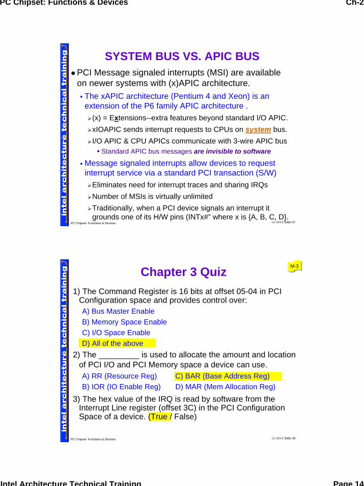
SYSTEM BUS VS. APIC BUSPCI Message signaled interrupts (MSI) are available on newer systems with (x)APIC architecture.
The xAPIC architecture (Pentium 4 and Xeon) is an extension of the P6 family APIC architecture .
(x) = Extensions--extra features beyond standard I/O APIC.xIOAPIC sends interrupt requests to CPUs on system bus. I/O APIC & CPU APICs communicate with 3-wire APIC bus
Standard APIC bus messages are invisible to software
Message signaled interrupts allow devices to request interrupt service via a standard PCI transaction (S/W)
Eliminates need for interrupt traces and sharing IRQs Number of MSIs is virtually unlimitedTraditionally, when a PCI device signals an interrupt it grounds one of its H/W pins (INTx#” where x is {A, B, C, D}.
CH-2 Slide-28PC Chipset: Functions & Devices
Chapter 3 Quiz1) The Command Register is 16 bits at offset 05-04 in PCI
Configuration space and provides control over:A) Bus Master EnableB) Memory Space EnableC) I/O Space Enable D) All of the above
2) The _________ is used to allocate the amount and location of PCI I/O and PCI Memory space a device can use.A) RR (Resource Reg) C) BAR (Base Address Reg) B) IOR (IO Enable Reg) D) MAR (Mem Allocation Reg)
3) The hex value of the IRQ is read by software from the Interrupt Line register (offset 3C) in the PCI Configuration Space of a device. (True / False)
M-3M-3

PC Chipset: Functions & Devices Ch-2
Intel Architecture Technical Training Page 15
CH-2 Slide-29PC Chipset: Functions & Devices
REVIEW & SUMMARYWindows ® Device Manager display.
Device manager allows users to view hardware devices and manage those hardware devices easily.
Displays IRQs, DMA, and Memory & I/O maps
Functions of the PCI Command registerCMD Reg (16 bits at offset 05-04) and provides control over device’s ability to respond to PCI accessesEnable I/O & memory accesses by setting bits 0 and 1
Memory space allocation using BARsBase Address Registers are used to allocate amount & location of PCI I/O and Memory space a device can use.
Power up system software (BIOS and or O/S) is responsible for initializing BARs in a resource conflict free manner.
CH-2 Slide-30PC Chipset: Functions & Devices
REVIEW & SUMMARYUse of PCI Interrupt Pin/Line Configuration Registers
PCI connector interrupts signals (INTA, B, C, D) will connect to 1 of 8 ICH interrupt inputs (PIRQA#-PIRQH#).Interrupt Pin at offset 3D; Interrupt Line at offset 3C
Interrupt Pin (3D): 01 for INTA; 02 for INTB Interrupt Line (3C): 17 -> IRQ17, 23 -> IRQ23
With the APIC (24 IRQs), most devices are assigned their own interrupts (e.g., IRQ16-23)
With standard ISA compatible 8259 PICs (15 IRQs), many devices share interrupts (for example IRQ 9).
End of Chapter 2End of Chapter 2