overview of the pic 16f648a processor: part 1 ee 361l—lab...
TRANSCRIPT
Galen Sasaki, Department of Electrical Engineering, University of Hawaii
1
Overview of the PIC 16F648A Processor: Part 1 EE 361L—Lab 2.1 Last update: August 19, 2011 Abstract: This report is the first of a three part series that discusses the features of the PIC 16F684A processor, which is from Microchip (www.microchip.com). The reports will refer to the data sheet of the processor. Each report takes about 30-60 minutes to read (this report will take 60 minutes). In this report, we review the basics of computer organization and technologies, and then cover some of the basic features of the processor. We also present a simple application of the processor to illustrate concepts. Finally, we will discuss bit-wise logic operations which are used in this and subsequent assignments.
Contents
1 Introduction to Computers and Computer Terminology .................................................................................................... 2
1.1 Programs ...................................................................................................................................................................... 2
1.2 Memory ........................................................................................................................................................................ 3
2 Processor Data Sheet .......................................................................................................................................................... 3
3 Example Application ............................................................................................................................................................ 7
3.1 Blinking LED Program ................................................................................................................................................... 8
3.2 Description of Some PIC Machine Instructions .......................................................................................................... 11
3.3 Delay Analysis of delay1ms ........................................................................................................................................ 13
3.4 Hardware .................................................................................................................................................................... 16
4 Important Pins ................................................................................................................................................................... 17
5 Registers ............................................................................................................................................................................ 17
6 Logic Operations ............................................................................................................................................................... 18
Appendix A Schmidt Trigger .................................................................................................................................................. 21

Galen Sasaki, Department of Electrical Engineering, University of Hawaii
2
1 Introduction to Computers and Computer Terminology The processor is a 18-pin computer in a chip with a
• Central processing unit (CPU): which runs the program, a collection of instructions that does some task. • Memory: which stores the program and holds variable values • Input/output (IO): which is how the chip interacts with the rest of the world.
1.1 Programs A program can be written using a high level language like C, such as in Figure 1.1.
Figure 1.1. Simple C language program.
This program has C language instructions such as “for” and “return”; variables such as “i” and “n”; and data constants such as “10” and “0”. Note that variables can be read and written to. However, the processor cannot run this program since it can only execute simpler instructions called machine instructions. Rather, the “high-level” C program must be compiled to create a machine program (or executable code or machine code), which is composed of machine instructions and can be executed by the processor. The machine instructions are from a machine language. For example, Intel processors follow the x86 machine language. The PIC has a different machine language with 35 instructions. A C language compiler (such as cc or gcc) is software that reads a C program, and then converts it to a machine program, composed of machine instructions. A C program is sometimes referred to as a source code because it can be compiled by different compilers, that are specific to different “target” processors. This will result in different machine programs. Machine instructions are strings of bits, which are difficult to read by humans. Assembly language is another way to write machine programs that can be read by humans. In assembly language, each machine instruction
main( ) { int i; int n; n = 0; for (i=0; i<10; i++) n = n*(n+1); return(); }
Galen Sasaki, Department of Electrical Engineering, University of Hawaii
3
has a mneumonic, which is a representation of an instruction that is easier to read. As an example, the PIC machine instruction 00000011000001 has the mneumonic CLRF 1. This instruction clears a variable “1”. Note that the mneumonic CLRF 1 is easier to read than the machine instruction 00000011000001. Assembly language programs are written in text, and they need to be assembled, which is the process of converting an assembly language program to an executable program. Assemblers are software that does the assembling.
1.2 Memory Programs and their variables are stored in the memory of the processor. Programs are stored in instruction memory or program memory, while variables and their data are stored in data memory. There are different types of memory technologies:
• Read only memory (ROM) can be read but not written to. Some ROM technologies can be written to (or programmed) only once, at the factory.
• Programmable ROMs (PROMs) can be programmed by the user. Many PROM technologies allow reprogramming, though the reprogramming is relatively slow.
• Erasable PROMs (EPROMS) can be erased by ultra violet light and then reprogrammed. You may have used EPROMS in EE 260.
• Electrically erasable PROMs (EEPROMs) are erasable using electricity. They are more convenient to reprogram since they do not require ultra violet light. A special type of EEPROM is flash memory, used in thumb drives.
• Random access memory (RAM) can be read and written to. PROMs are known as non-volatile memory since the circuit can be turned off and the data is still retained. RAM is referred to as volatile memory since when turned off, all the data is lost.
2 Processor Data Sheet The PIC 16F684A has a data sheet. Page 3 of the data sheet has a list of the PIC’s features. The following are some of these features:
• 35 single-word instructions • Interrupt capability • 18 pin dual-in line package • Internal and external oscillator options • Power-saving Sleep mode • Watchdog Timer with independent oscillator for reliable operation

Galen Sasaki, Department of Electrical Engineering, University of Hawaii
4
• In-Circuit Serial Programming (ICSP) • Power-on Reset • Wide operating voltage range (2.0v - 5.5v)
Figure 2.1. Snapshot of a portion of page 3 of the datasheet. Page 4 of the datasheet has the pin diagram as shown in Figure 2.2. Note that many of the pins have multiple names. For example, Pin 2 has the label RA3/AN3/CMP1, which means it has one of four possible functions. RA3 is an IO port, AN3 is an input for a analog comparator, and CMP1 is an output for comparator. A programmer can choose one of the three functions through the source code. An explanation of these pins is given on pages 13-14. A portion of pages 13 and 14 is shown in Figure 2.3. We will only have time to cover a subset of these functions.

Galen Sasaki, Department of Electrical Engineering, University of Hawaii
5
Figure 2.2. Pin diagram of the PIC from the data sheet.
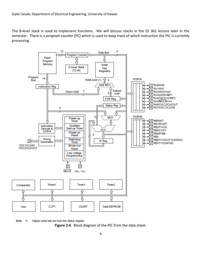
Figure 2.3. A portion of pages 13 and 14 from the data sheet. Page 12 of the data sheet has a schematic diagram of the processor as shown in Figure 2.4. The top of the page shows 4096 x 14 of flash memory, which is used as program memory. Each machine instruction is 14 bits, and there can be 4096 instructions. There is also 256 bytes of RAM. Each data is 1 byte, and there are 256 memory cells. These cells can be used for variables. For example, in Figure 1 the dummy variable “i” in the for-loop can be implemented in RAM. Thus, the program memory is used to store instructions (which are referred to as operations) and RAM is used to store data (which are referred to as operands).
Galen Sasaki, Department of Electrical Engineering, University of Hawaii
6
The 8-level stack is used to implement functions. We will discuss stacks in the EE 361 lecture later in the semester. There is a program counter (PC) which is used to keep track of which instruction the PIC is currently processing.
Figure 2.4. Block diagram of the PIC from the data sheet.
Galen Sasaki, Department of Electrical Engineering, University of Hawaii
7
On the right side of the diagram are PORTA and PORTB. These are I/O ports used to connect the processor with the outside world. In the middle of the diagram is a block of components: Power-up Timer, Oscillator Start-up Timer, Power-on Reset, Watchdog Timer, and Brown-out Reset. These components deal with resetting the processor. For example, the Brown-out Reset deals the following situation. When the source voltage to the processor is too low, e.g., instead at full 5v the power temporarily goes to say 1.8v, the processor’s circuits may not behave properly. As a result, the processor will not behave correctly even when full power is restored. The Brown-out Reset will detect this low power situation and automatically reset the processor so it is runs properly again. To the left of Figure 2.4 are the Timer Generation and Internal Timing Block which are the sources of the clock signal for the processor. The PIC like all processors is a synchronous digital circuit and operates on a clock signal. The PIC has multiple options for clock signals. It can use an internally generated clock signal or an external source. The internal signal is convenient but less accurate. An external signal can be generated using a crystal. For this lab, we will use an oscillator crystal as shown in Figure 2.5.
Figure 2.5. Oscillator crystals. At the bottom of Figure 2.4 are timer components. These are basically counter circuits, similar to the 74163 circuits from EE 260. We will use one of these in a lab assignment. Also at the bottom is an EEPROM which is nonvolatile memory used to store data. Note that this is different than program memory which stores machine instructions. There are also an analog comparator circuits and a USART. We will ignore these for EE 361L.
3 Example Application In the next subsection, we will discuss a simple example application which has the processor drive an LED so that it blinks periodically. The application uses IO ports. The program of the application is written in C language but there is also an assembly language portion. In Subsection 3.2, we will explain some of the assembly language instructions.

Galen Sasaki, Department of Electrical Engineering, University of Hawaii
8
3.1 Blinking LED Program The following program called the “Blinking LED program” is a simple example that has IO. It assumes that an LED is attached to pin RA1, and it turns the LED on and off. The RA1 pin is part of the 8-bit wide PORTA. The bits of PORTA are RA7, RA6,..., RA0. PORTA can be treated as a variable in software. main( ) // BLINKING LED program { // Set PORTA so that RA3 and RA2 are inputs, and RA5, RA4, RA1, and RA0 are outputs. TRISA = 0x04; // Prefix “0x” means hexadecimal. Note that “0” is a zero, not the // alphabet “O” while(1) { // Loop forever PORTA = 0x00; // Output 0 to RA1 PORTA = 0x02; // Output 1 to RA1 } } PORTA is bidirectional which means its bits can be configured to be inputs or outputs. These bits can be configured in software by another variable TRISA. Setting a bit in TRISA to 0 will make the corresponding bit in PORTA an output. Setting the bit to 1 will make the bit an input. The Blinking LED program sets RA1 to be an output, which is done in the instruction TRISA = 0x04. The number “0x04” is a hexadecimal number, where “0x” prefix indicates hexadecimal. The base in hexadecimal numbers is 16, and each digit represents a value from 0 to 15. The digits are 0, 1, 2, ..., 9, A, B, ..., F, where the digits A = 10, B = 11, ..., F = 15. A hexadecimal number 021 ...hhh nn −− has value
00
22
11 16...1616 ×++×+× −
−−
− hhh nn
nn . Hexadecimal numbers are a convenient way to represent binary
numbers. Each hexadecimal digit represents four bits. For example, the hexadecimal number F5 can be converted to binary by converting each digit to four bits. F equals 15, which in binary is 1111, and 5 equals 0101. The representation of F5 in binary is 11110101. The following table converts hexadecimal digits to binary numbers
Hex Binary Hex Binary Hex Binary Hex Binary 0 0000 4 0100 8 1000 c 1100 1 0001 5 0101 9 1001 d 1101 2 0010 6 0110 a 1010 e 1110 3 0011 7 0111 b 1011 f 1111
The instruction TRISA = 0x04 indicates that the ports are configured using the binary string 0000 0100 (which equals 0x04). Thus, RA2 is configured to be an input while all the other ports are configured to be outputs.

Galen Sasaki, Department of Electrical Engineering, University of Hawaii
9
TRISA is implemented by a hardware register. Such registers are often called control registers. To the C compiler for the PIC, “ TRISA” and “PORTA” are variables with special names. After the Blinking LED program configures PORTA to inputs and outputs, it goes into an infinite loop, continually setting pin RA1 to the value 0 and then 1. There is a problem with this program. Since the processor is running so fast, the LED will blink very quickly, too fast for humans to detect. We will just see an LED that seems continually on. This can be solved by adding delay as shown in the next program, “Blinking LED 2”. main( ) // BLINKING LED 2 program { // Set PORTA so that RA3 and RA2 are inputs, and RA5, RA4, RA1, and RA0 are outputs. TRISA = 0x04; // Prefix “0x” means hexadecimal. Note that “0” is a zero, not the // alphabet “O” while(1) { // Loop forever PORTA = 0x00; // Output 0 to RA1 delay1sec(); // Delay 1 second PORTA = 0x02; // Output 1 to RA1 delay1sec(); // Delay 1 second } } The Blinking LED 2 program uses a function “delay1sec”, which provides a 1 second delay. Next, we will discuss implementing this function. The following implementation is a naive approach. It assumes a 1 MHz clock (note that in the actual lab assignment, the clock rate may be different). The function has a for-loop that goes through 1 million passes. void delay1sec( ) // A delay of 1 second { int n; n = 0; while (n < 1000000){ // 1000000 = 1 million passes of the while loop n++; } } If each pass takes one clock cycle (1 us) then the for-loop will cause 1 second of delay. However, this function will not work for the following reasons:
• Each line of C will translate into multiple lines of machine instructions. It is difficult to estimate the number of instructions without compiling.
• Machine instructions can take multiple clock cycles, and some instructions will take different clock cycles depending on the situation.
Galen Sasaki, Department of Electrical Engineering, University of Hawaii
10
• The variable “n” is stored in a memory cell (register), and this cell has a limited size of 8 bits. Its value ranges from -128 to +127 (using twos complement arithmetic; if you don’t know twos complement, we will discuss this in lecture later). Thus, “n” cannot be implemented correctly in the for-loop, which requires it to range up to 1 million.
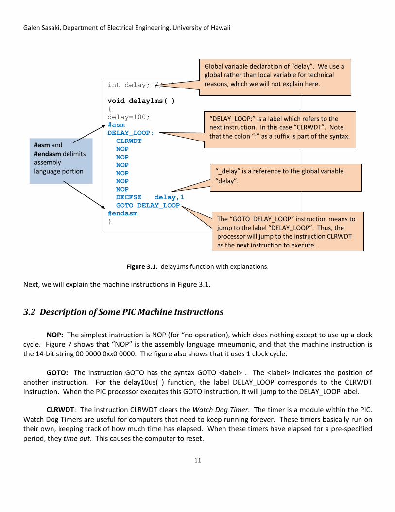
Next, we will implement the 1 second delay using two functions. The first function “delay1sec” calls a second function “delay1ms”, that has a 1 millisecond delay. The function “delay1sec” calls “delay1ms” for 1000 times. The following is “delay1sec”. The C instruction “for” and calculations such as “n++” take clock cycles too but but just a small percentage compared to “delay1ms”. void delay1sec( ) // A delay of 1 second { int n,m; for (n=0; n<10; n++) { for (m=0; m<100; m++) delay1ms( ); } } Figure 3 has the “delay1ms” C function which also has assembly language instructions. The compiler for the PIC allows a program to have a mix of C language and assembly language. By writing most of the function in assembly language, we can control the number of clock cycles. Figure 3.1 shows how the assembly language portion is delimited. It also explains the “DELAY_LOOP” label. The assembly language portion is a delay loop. It is composed of the assembly language instructions CLRWDT, NOP, DECFSZ, and GOTO. (The PIC has 35 machine instructions, which are presented in Section 15 in the data sheet, starting from page 117.)
Galen Sasaki, Department of Electrical Engineering, University of Hawaii
11
Figure 3.1. delay1ms function with explanations.
Next, we will explain the machine instructions in Figure 3.1.
3.2 Description of Some PIC Machine Instructions NOP: The simplest instruction is NOP (for “no operation), which does nothing except to use up a clock cycle. Figure 7 shows that “NOP” is the assembly language mneumonic, and that the machine instruction is the 14-bit string 00 0000 0xx0 0000. The figure also shows that it uses 1 clock cycle. GOTO: The instruction GOTO has the syntax GOTO <label> . The <label> indicates the position of another instruction. For the delay10us( ) function, the label DELAY_LOOP corresponds to the CLRWDT instruction. When the PIC processor executes this GOTO instruction, it will jump to the DELAY_LOOP label. CLRWDT: The instruction CLRWDT clears the Watch Dog Timer. The timer is a module within the PIC. Watch Dog Timers are useful for computers that need to keep running forever. These timers basically run on their own, keeping track of how much time has elapsed. When these timers have elapsed for a pre-specified period, they time out. This causes the computer to reset.
int delay; // This is a global variable void delay1ms( ) { delay=100; #asm DELAY_LOOP: CLRWDT NOP NOP NOP NOP NOP NOP DECFSZ _delay,1 GOTO DELAY_LOOP #endasm }
#asm and #endasm delimits assembly language portion
“DELAY_LOOP:” is a label which refers to the next instruction. In this case “CLRWDT”. Note that the colon “:” as a suffix is part of the syntax.
The “GOTO DELAY_LOOP” instruction means to jump to the label “DELAY_LOOP”. Thus, the processor will jump to the instruction CLRWDT as the next instruction to execute.
“_delay” is a reference to the global variable “delay”.
Global variable declaration of “delay”. We use a global rather than local variable for technical reasons, which we will not explain here.
Galen Sasaki, Department of Electrical Engineering, University of Hawaii
12
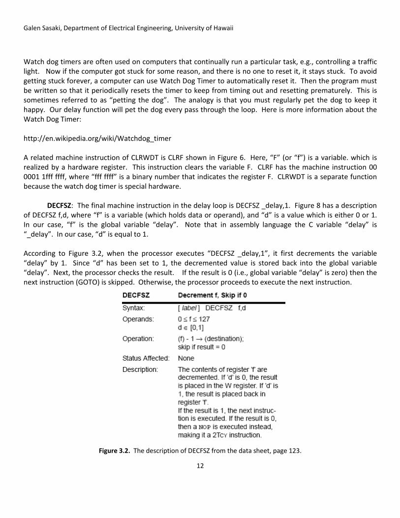
Watch dog timers are often used on computers that continually run a particular task, e.g., controlling a traffic light. Now if the computer got stuck for some reason, and there is no one to reset it, it stays stuck. To avoid getting stuck forever, a computer can use Watch Dog Timer to automatically reset it. Then the program must be written so that it periodically resets the timer to keep from timing out and resetting prematurely. This is sometimes referred to as “petting the dog”. The analogy is that you must regularly pet the dog to keep it happy. Our delay function will pet the dog every pass through the loop. Here is more information about the Watch Dog Timer: http://en.wikipedia.org/wiki/Watchdog_timer A related machine instruction of CLRWDT is CLRF shown in Figure 6. Here, “F” (or “f”) is a variable. which is realized by a hardware register. This instruction clears the variable F. CLRF has the machine instruction 00 0001 1fff ffff, where “fff ffff” is a binary number that indicates the register F. CLRWDT is a separate function because the watch dog timer is special hardware. DECFSZ: The final machine instruction in the delay loop is DECFSZ _delay,1. Figure 8 has a description of DECFSZ f,d, where “f” is a variable (which holds data or operand), and “d” is a value which is either 0 or 1. In our case, “f” is the global variable “delay”. Note that in assembly language the C variable “delay” is “_delay”. In our case, “d” is equal to 1. According to Figure 3.2, when the processor executes “DECFSZ _delay,1”, it first decrements the variable “delay” by 1. Since “d” has been set to 1, the decremented value is stored back into the global variable “delay”. Next, the processor checks the result. If the result is 0 (i.e., global variable “delay” is zero) then the next instruction (GOTO) is skipped. Otherwise, the processor proceeds to execute the next instruction.
Figure 3.2. The description of DECFSZ from the data sheet, page 123.

Galen Sasaki, Department of Electrical Engineering, University of Hawaii
13
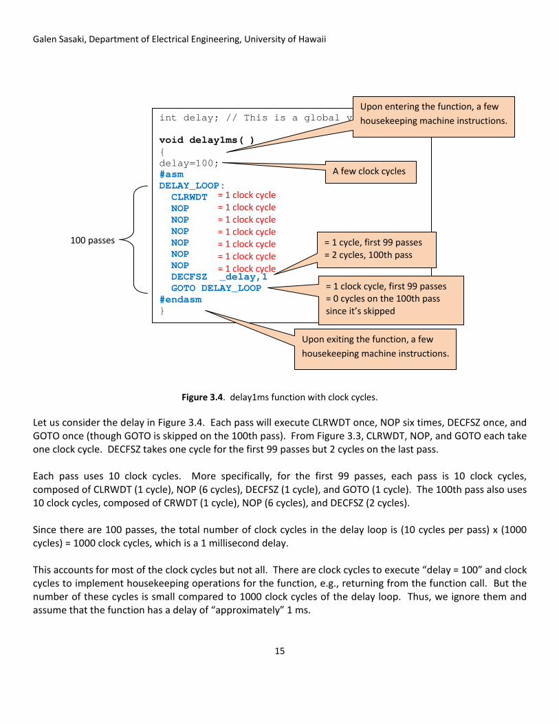
3.3 Delay Analysis of delay1ms Figure 5 shows the function “delay1ms” again with an explanation of the number of clock cycles it uses. It has the following components:
• The C instruction “delay = 100” initializes the variable “delay”. • The assembly language portion is a delay loop. Each time the delay loop is passed, the instruction
DECFSZ decrements “delay”. Thus, the loop goes through 100 passes. The data sheet of the PIC shows the number of cycles per instruction on page 118 under “Table 15-2”. The table is shown in Figure 3.3.

Galen Sasaki, Department of Electrical Engineering, University of Hawaii
14
Figure 3.3. The table from page 118 from the PIC data sheet.
Galen Sasaki, Department of Electrical Engineering, University of Hawaii
15
Figure 3.4. delay1ms function with clock cycles. Let us consider the delay in Figure 3.4. Each pass will execute CLRWDT once, NOP six times, DECFSZ once, and GOTO once (though GOTO is skipped on the 100th pass). From Figure 3.3, CLRWDT, NOP, and GOTO each take one clock cycle. DECFSZ takes one cycle for the first 99 passes but 2 cycles on the last pass. Each pass uses 10 clock cycles. More specifically, for the first 99 passes, each pass is 10 clock cycles, composed of CLRWDT (1 cycle), NOP (6 cycles), DECFSZ (1 cycle), and GOTO (1 cycle). The 100th pass also uses 10 clock cycles, composed of CRWDT (1 cycle), NOP (6 cycles), and DECFSZ (2 cycles). Since there are 100 passes, the total number of clock cycles in the delay loop is (10 cycles per pass) x (1000 cycles) = 1000 clock cycles, which is a 1 millisecond delay. This accounts for most of the clock cycles but not all. There are clock cycles to execute “delay = 100” and clock cycles to implement housekeeping operations for the function, e.g., returning from the function call. But the number of these cycles is small compared to 1000 clock cycles of the delay loop. Thus, we ignore them and assume that the function has a delay of “approximately” 1 ms.
int delay; // This is a global variable void delay1ms( ) { delay=100; #asm DELAY_LOOP: CLRWDT NOP NOP NOP NOP NOP NOP DECFSZ _delay,1 GOTO DELAY_LOOP #endasm }
= 1 cycle, first 99 passes = 2 cycles, 100th pass
A few clock cycles
= 1 clock cycle = 1 clock cycle = 1 clock cycle = 1 clock cycle = 1 clock cycle = 1 clock cycle = 1 clock cycle
= 1 clock cycle, first 99 passes = 0 cycles on the 100th pass since it’s skipped
Upon entering the function, a few housekeeping machine instructions.
Upon exiting the function, a few housekeeping machine instructions.
100 passes
Galen Sasaki, Department of Electrical Engineering, University of Hawaii
16
Note that the number of NOPs in the function was determined as part of its design. The number of NOPS used is just enough so that the function has a 1 ms delay. If we wanted more or less delay we would add or delete NOPs.
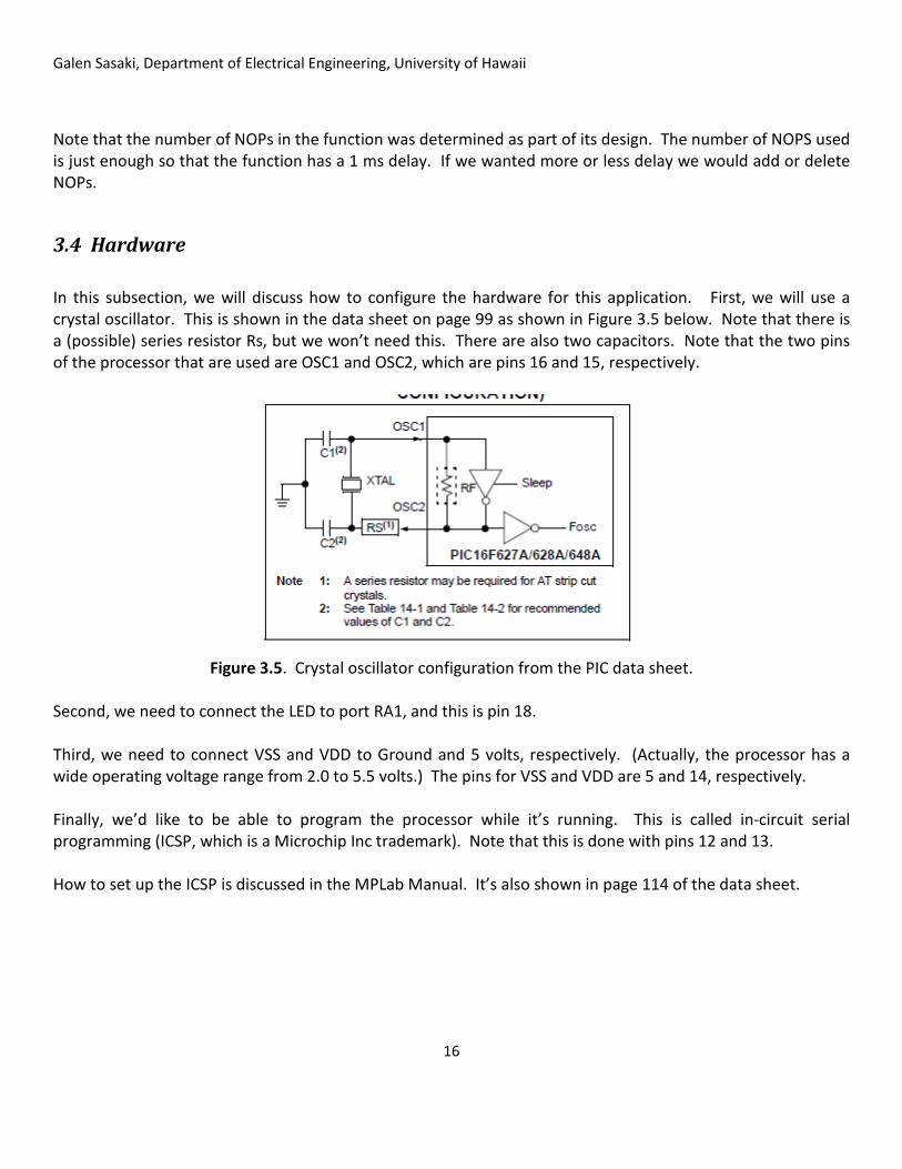
3.4 Hardware In this subsection, we will discuss how to configure the hardware for this application. First, we will use a crystal oscillator. This is shown in the data sheet on page 99 as shown in Figure 3.5 below. Note that there is a (possible) series resistor Rs, but we won’t need this. There are also two capacitors. Note that the two pins of the processor that are used are OSC1 and OSC2, which are pins 16 and 15, respectively.
Figure 3.5. Crystal oscillator configuration from the PIC data sheet.
Second, we need to connect the LED to port RA1, and this is pin 18. Third, we need to connect VSS and VDD to Ground and 5 volts, respectively. (Actually, the processor has a wide operating voltage range from 2.0 to 5.5 volts.) The pins for VSS and VDD are 5 and 14, respectively. Finally, we’d like to be able to program the processor while it’s running. This is called in-circuit serial programming (ICSP, which is a Microchip Inc trademark). Note that this is done with pins 12 and 13. How to set up the ICSP is discussed in the MPLab Manual. It’s also shown in page 114 of the data sheet.

Galen Sasaki, Department of Electrical Engineering, University of Hawaii
17
4 Important Pins Here is a list of important pins.
• PORTA (RA0 – RA7) and PORTB (RB0 – RB7): Bidirectional I/O ports. • OSC1 and OSC2: Inputs for the crystal oscillator. • INT: External interrupt. We’ll learn more about interrupts later. Some of the pins of PORTB can also
function as interrupts. • PGC and PGD: ICSP programming Clock and Data. Used in in-circuit programming • VSS: Ground reference. • VDD: Power supply. • \MCLR: Master clear (it should have an overbar over MCLR but I couldn’t get it to work on word doc).
When configured this is an active-low Reset to the processor. Note that, at various places, there is a reference to Schmidt triggers in the data sheet. Appendix A describes what a Schmidt trigger is.
5 Registers
• PORTA and PORTB: Bidirectional ports RA and RB and some of the ports can be configured as interrupts.
• TRISA and TRISB: Programming these registers with 0s and 1s can configure the RA and RB ports as outputs and inputs respectively. Its value on reset is 1s, which implies the default on the I/O ports is as inputs.
• OPTION_REG: This is to configure ports and the timer circuit TMR0. We’ll use this later. It’s default value on Reset is to disable the functions, which is fine for now.
• INTCON: This configures the interrupts. We’ll consider this later on another lab assignment. It’s default value on Reset is to disable the interrupts, which is fine for now.
• PIE1 and PIR1: These are configuration registers for components we won’t use so ignore. • PCON: This is the power control register. We won’t be using this either so we’ll ignore it.
Galen Sasaki, Department of Electrical Engineering, University of Hawaii
18
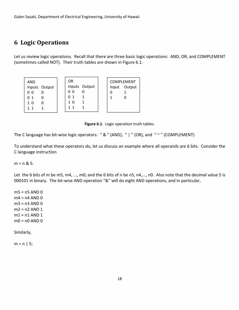
6 Logic Operations Let us review logic operations. Recall that there are three basic logic operations: AND, OR, and COMPLEMENT (sometimes called NOT). Their truth tables are shown in Figure 6.1.
Figure 6.1. Logic operation truth tables. The C language has bit-wise logic operators: “ & ” (AND), “ | ” (OR), and “ ~ ” (COMPLEMENT) To understand what these operators do, let us discuss an example where all operands are 6 bits. Consider the C language instruction m = n & 5. Let the 6 bits of m be m5, m4, ..., m0; and the 6 bits of n be n5, n4,..., n0. Also note that the decimal value 5 is 000101 in binary. The bit-wise AND operation “&” will do eight AND operations, and in particular, m5 = n5 AND 0 m4 = n4 AND 0 m3 = n3 AND 0 m2 = n2 AND 1 m1 = n1 AND 1 m0 = n0 AND 0 Similarly, m = n | 5;
AND Inputs Output 0 0 0 0 1 0 1 0 0 1 1 1
OR Inputs Output 0 0 0 0 1 1 1 0 1 1 1 1
COMPLEMENT Input Output 0 1 1 0

Galen Sasaki, Department of Electrical Engineering, University of Hawaii
19
results in m5 = n5 OR 0 m4 = n4 OR 0 m3 = n3 OR 0 m2 = n2 OR 1 m1 = n1 OR 0 m0 = n0 OR 1 Likewise, the bit-wise complement operation “ ~ “ will just flip all the bits. The logic operations can be very useful in processors. The AND operation can clear bits to 0, and the OR operation can set bits to 1. For example, m = n & 5 results in m = (0, 0, 0, n2, 0, n0) Here, the binary value for 5 is (0 0 0 1 0 1), and so bits 0 and 2 are one while the rest of the bits are zero. Note that if you AND a bit x with zero then the result is always zero; while if you AND a bit x with one then the result is the bit x again. Thus, the operation m = n & 5 will clear all bits except bits 0 and 2. The bit string (0 0 0 1 0 1) is referred to a mask because it will mask out bits. Similarly, the bit-wise OR operation “ | “ can be used to set bits to 1. Here, 0s result in unchanged values, while 1s result in bits being set to 1. Some other useful C language operators are the bit shifting operators “<<” and “>>”, which are left and right shifts respectively. Let us go over the left shift operation first. Consider the C language instruction m = n << 2 This means that the value of n = ( n5, n4, ..., n0) should be shifted to the left by 2 bit positions. This results in m = (n3, n2, n1, n0, 0, 0). The right shift “>>” works in a similar way except the bits are shifted to the right. Now as a review, we will give some examples that combine all of the operations above. Consider the C language instructions d = 1 << 3; m = m | d;

Galen Sasaki, Department of Electrical Engineering, University of Hawaii
20
The first line ” d = 1 << 3” will shift the value “1” to the left by 3 bit positions. Recall that “1” in binary is 00000001. Shifting this to the left by 3 bit positions leaves 00001000. Thus, d = 00001000. This is also our mask. The second line “m = m | d” will bit-wise OR the mask with variable m. Since the mask has value 1 at bit position 3, m3 will be set to 1, while the rest of variable m will be unchanged. We can rewrite this more compactly by the single line m = m | (1 << 3); or alternatively m |= (1 << 3); Note that these lines will set m3 to 1, and leave the rest of variable m unchanged. If instead we wanted to set m6 to 1, we could write m |= (1 << 6); Now we will show how the bit-wise AND operation can be used to clear bits. Consider the C language instructions d = 1 << 3; d = ~d; m = m & d; The first line ” d = 1 << 3” will leave d = 00001000. The second line “d = ~d” will leave d = 11110111. This is our mask. The third line “m = m & d” will bit-wise AND the mask with variable m. Since the mask has value 0 at bit position 3, m3 will be cleared to 0, while the rest of variable m will be unchanged. We can rewrite this more compactly by the single line m = m & (~(1 << 3)); or alternatively m &= (~(1 << 3)); Note that these lines will clear m3 to 0, and leaving the rest of variable m unchanged. If instead we wanted to clear m6, we could write m &= (~(1 << 6)); Finally, note that we use the term “clear” to mean setting a value to 0, and the term “set” to mean setting a value to 1. Though this is not a standard terminology, it is used in technical documents frequently. Sometimes documents will just state “set” and assume you know that it means “set to the value 1”, and “clear” to mean “clear to the value 0”. This does not happen all the time but be aware of it.
Galen Sasaki, Department of Electrical Engineering, University of Hawaii
21
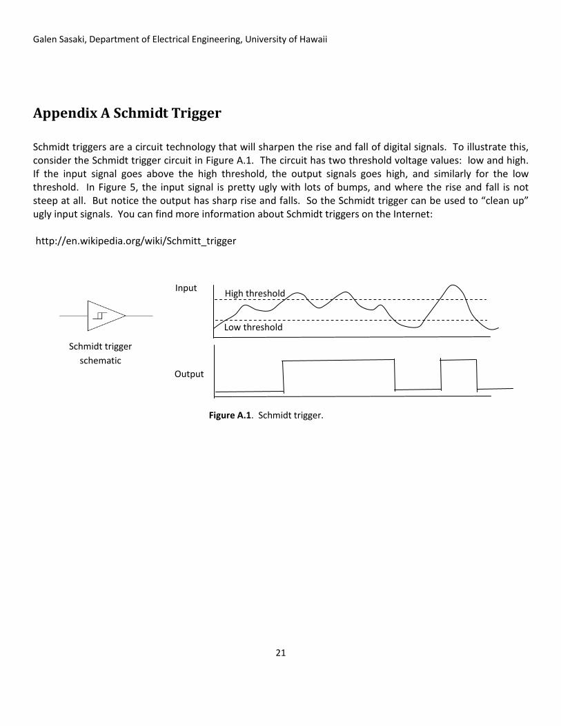
Appendix A Schmidt Trigger Schmidt triggers are a circuit technology that will sharpen the rise and fall of digital signals. To illustrate this, consider the Schmidt trigger circuit in Figure A.1. The circuit has two threshold voltage values: low and high. If the input signal goes above the high threshold, the output signals goes high, and similarly for the low threshold. In Figure 5, the input signal is pretty ugly with lots of bumps, and where the rise and fall is not steep at all. But notice the output has sharp rise and falls. So the Schmidt trigger can be used to “clean up” ugly input signals. You can find more information about Schmidt triggers on the Internet: http://en.wikipedia.org/wiki/Schmitt_trigger
Schmidt trigger schematic
Input High threshold
Low threshold
Output
Figure A.1. Schmidt trigger.