university of hawaii ee 361l getting started with spartan...
TRANSCRIPT
1
University of Hawaii EE 361L Getting Started with Spartan 3E Digilent Board
Contents I. Hardware and Software Requirements ............................................................................................................... 2 II. Getting Started ................................................................................................................................................... 2 III. Create a New Project ....................................................................................................................................... 3 IV. Create an HDL Source ..................................................................................................................................... 4 V. Design Simulation ............................................................................................................................................. 6 VI. Create Timing Constraints ............................................................................................................................. 10 VII. Implement Design and Verify Constraints ................................................................................................... 12 VIII. Reimplement Design and Verify Pin Locations ......................................................................................... 15 IX. Download Design to the Digilent Board ....................................................................................................... 15

2
I. Hardware and Software Requirements Software Requirements To use this tutorial, you must install the following software: ISE 10.1 For more information about installing Xilinx® software, see the ISE Release Notes and Installation Guide at: http://www.xilinx.com/support/software_manuals.htm. Hardware Requirements To use this tutorial, you must have the following hardware:
• Spartan-3E Startup Kit, containing the Spartan-3 Startup Kit Demo Board
II. Getting Started Starting the ISE Software To start ISE, double-click the desktop icon, or start ISE from the Start menu by selecting: Start → All Programs → Xilinx ISE 10.1→ Project Navigator Note: Your start-up path is set during the installation process and may differ from the one above. Accessing Help At any time during the tutorial, you can access online help for additional information about the ISE software and related tools. To open Help, do either of the following:
• Press F1 to view Help for the specific tool or function that you have selected or highlighted. • Launch the ISE Help Contents from the Help menu. It contains information about creating and
maintaining your complete design flow in ISE.

3
Figure 1: ISE Help Topics.
III. Create a New Project Create a new ISE project which will target the FPGA device on the Spartan-3E Startup Digilent board. To create a new project: • Select File > New Project... The New Project Wizard appears. • Type tutorial in the Project Name field. • Enter or browse to a location (directory path) for the new project. A tutorial subdirectory is created
automatically. • Verify that HDL is selected from the Top-Level Source Type list. • Click Next to move to the device properties page. • Fill in the properties in the table as shown below:
o Product Category: All o Family: Spartan3E o Device: XC3S100E o Package: TQ144 o Speed Grade: -4 o Top-Level Source Type: HDL o Synthesis Tool: XST (VHDL/Verilog) o Simulator: ISE Simulator (VHDL/Verilog) o Preferred Language: Verilog o Verify that Enable Enhanced Design Summary is selected.
Leave the default values in the remaining fields. When the table is complete, your project properties will look like the following:
Figure 2: Project Device Properties.

4
7. Click Next to proceed to the Create New Source window in the New Project Wizard. At the end of the next section, your new project will be complete.
IV. Create an HDL Source In this section, you will create the top-level HDL file for your design. Determine the language that you wish to use for the tutorial. Then, continue either to the “Creating a VHDL Source” section below, or skip to the “Creating a Verilog Source” section. Creating a Verilog Source Create the top-level Verilog source file for the project as follows: • Click New Source in the New Project dialog box. • Select Verilog Module as the source type in the New Source dialog box. • Type in the file name counter. • Verify that the Add to Project checkbox is selected. • Click Next. • Declare the ports for the counter design by filling in the port information as shown below:
Figure 3: Define Module. • Click Next, then Finish in the New Source Information dialog box to complete the new source file template. • Click Next, then Next, then Finish. The source file containing the counter module displays in the Workspace, and the counter displays in the Sources tab, as shown below:

5
Figure 4: New Project in ISE. Using Language Templates (Verilog) The next step in creating the new source is to add the behavioral description for counter. Use a simple counter code example from the ISE Language Templates and customize it for the counter design. • Place the cursor on the line below the output [3:0] COUNT_OUT; statement. • Open the Language Templates by selecting Edit → Language Templates… Note: You can tile the
Language Templates and the counter file by selecting Window → Tile Vertically to make them both visible.
• Using the “+” symbol, browse to the following code example:
Verilog → Synthesis Constructs → Coding Examples → Counters → Binary → Up/Down Counters → Simple Counter Create an HDL Source R
• With Simple Counter selected, select Edit → Use in File, or select the Use Template in File toolbar button.
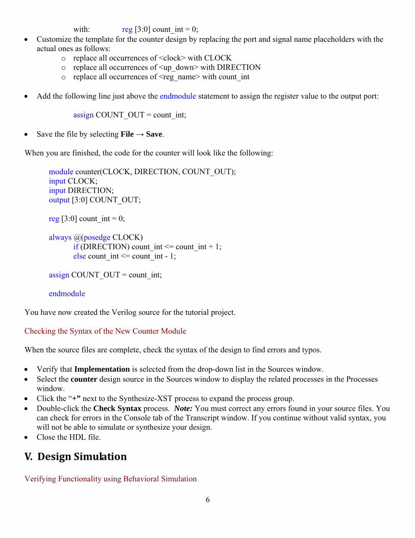
This step copies the template into the counter source file. • Close the Language Templates. Final Editing of the Verilog Source • To declare and initialize the register that stores the counter value, modify the declaration statement in the
first line of the template as follows: replace: reg [<upper>:0] <reg_name>;
6
with: reg [3:0] count_int = 0; • Customize the template for the counter design by replacing the port and signal name placeholders with the
actual ones as follows: o replace all occurrences of <clock> with CLOCK o replace all occurrences of <up_down> with DIRECTION o replace all occurrences of <reg_name> with count_int
• Add the following line just above the endmodule statement to assign the register value to the output port:
assign COUNT_OUT = count_int;
• Save the file by selecting File → Save. When you are finished, the code for the counter will look like the following:
module counter(CLOCK, DIRECTION, COUNT_OUT); input CLOCK; input DIRECTION; output [3:0] COUNT_OUT; reg [3:0] count_int = 0; always @(posedge CLOCK)
if (DIRECTION) count_int <= count_int + 1; else count_int <= count_int - 1;
assign COUNT_OUT = count_int; endmodule
You have now created the Verilog source for the tutorial project. Checking the Syntax of the New Counter Module When the source files are complete, check the syntax of the design to find errors and typos. • Verify that Implementation is selected from the drop-down list in the Sources window. • Select the counter design source in the Sources window to display the related processes in the Processes
window. • Click the “+” next to the Synthesize-XST process to expand the process group. • Double-click the Check Syntax process. Note: You must correct any errors found in your source files. You
can check for errors in the Console tab of the Transcript window. If you continue without valid syntax, you will not be able to simulate or synthesize your design.
• Close the HDL file.
V. Design Simulation Verifying Functionality using Behavioral Simulation

7
Create a test bench waveform containing input stimulus you can use to verify the functionality of the counter module. The test bench waveform is a graphical view of a test bench. Create the test bench waveform as follows: • Select the counter HDL file in the Sources window. • Create a new test bench source by selecting Project → New Source. • In the New Source Wizard, select Test Bench WaveForm as the source type, and type counter_tbw in the
File Name field. Click Next. • The Associated Source page shows that you are associating the test bench waveformwith the source file
counter. Click Next. • The Summary page shows that the source will be added to the project, and it displays the source directory,
type, and name. Click Finish. • You need to set the clock frequency, setup time and output delay times in the Initialize Timing dialog box
before the test bench waveform editing window opens. The requirements for this design are the following: • The counter must operate correctly with an input clock frequency = 25 MHz. • The DIRECTION input will be valid 10 ns before the rising edge of CLOCK. • The output (COUNT_OUT) must be valid 10 ns after the rising edge of CLOCK. The design requirements correspond with the values below. Fill in the fields in the Initialize Timing dialog box with the following information: • Clock High Time: 20 ns. • Clock Low Time: 20 ns. • Input Setup Time: 10 ns. • Output Valid Delay: 10 ns. • Offset: 0 ns. • Global Signals: GSR (FPGA). Note: When GSR(FPGA) is enabled, 100 ns. is added to the Offset value
automatically. • Initial Length of Test Bench: 1500 ns. Leave the Default Value in the remaining

8
Figure 5: Initialize Timing. • Click Finish to complete the timing initialization. • The blue shaded areas that precede the rising edge of the CLOCK correspond to the Input Setup Time in the
Initialize Timing dialog box. Toggle the DIRECTION port to define the input stimulus for the counter design as follows:
• Click on the blue cell at approximately the 300 ns to assert DIRECTION high so that the counter will
count up. • Click on the blue cell at approximately the 900 ns to assert DIRECTION low so that the counter will
count down. Note: For more accurate alignment, you can use the Zoom In and Zoom Out toolbar buttons.

9
Figure 6: Simulation Waveform.
• Save the waveform. • In the Sources window, select the Behavioral Simulation view to see that the test bench waveform file is
automatically added to your project.
Figure 7: Chose Post-Route Simulation. • Close the test bench waveform. Simulating Design Functionality Verify that the counter design functions as you expect by performing behavior simulation as follows: • Verify that Behavioral Simulation and counter_tbw are selected in the Sources window. • In the Processes tab, click the “+” to expand the Xilinx ISE Simulator process and double-click the
Simulate Behavioral Model process. The ISE Simulator opens and runs the simulation to the end of the test bench.
• To view your simulation results, select the Simulation tab and zoom in on the transitions. The simulation waveform results will look like the following:
Figure 8: Test Bench Waveform. Note: You can ignore any rows that start with TX.
• Verify that the counter is counting up and down as expected.

10
• Close the simulation view. If you are prompted with the following message, “You have an active simulation open. Are you sure you want to close it?“, click Yes to continue.
You have now completed simulation of your design using the ISE Simulator.
VI. Create Timing Constraints Specify the timing between the FPGA and its surrounding logic as well as the frequency the design must operate at internal to the FPGA. The timing is specified by entering constraints that guide the placement and routing of the design. It is recommended that you enter global constraints. The clock period constraint specifies the clock frequency at which your design must operate inside the FPGA. The offset constraints specify when to expect valid data at the FPGA inputs and when valid data will be available at the FPGA outputs. Entering Timing Constraints To constrain the design do the following: • Select Implementation from the drop-down list in the Sources window. • Select the counter HDL source file. • Click the “+” sign next to the User Constraints processes group, and double-click the Create Timing
Constraints process. ISE runs the Synthesis and Translate steps and automatically creates a User Constraints File (UCF). You will be prompted with the following message:
Figure 9: Prompt to Add UCF File to Project. • Click Yes to add the UCF file to your project.
The counter.ucf file is added to your project and is visible in the Sources window. The Xilinx Constraints Editor opens automatically. Note: You can also create a UCF file for your project by selecting Project → Create New Source.
• In the Timing Constraints dialog, enter the following in the Period, Pad to Setup, and CLock to Pad fields: o Period: 40 o Pad to Setup: 10 o Clock to Pad: 10
• Press Enter.
11
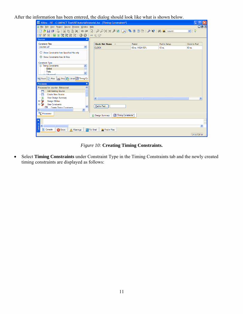
After the information has been entered, the dialog should look like what is shown below.
Figure 10: Creating Timing Constraints. • Select Timing Constraints under Constraint Type in the Timing Constraints tab and the newly created
timing constraints are displayed as follows:

12
Figure 11: Timing Constraints. • Save the timing constraints. If you are prompted to rerun the TRANSLATE or XST step, click OK to
continue. • Close the Constraints Editor.
VII. Implement Design and Verify Constraints Implement the design and verify that it meets the timing constraints specified in the previous section. Implementing the Design • Select the counter source file in the Sources window. • Open the Design Summary by double-clicking the View Design Summary process in the Processes tab. • Double-click the Implement Design process in the Processes tab. • Notice that after Implementation is complete, the Implementation processes have a green check mark next to
them indicating that they completed successfully without Errors or Warnings.
13
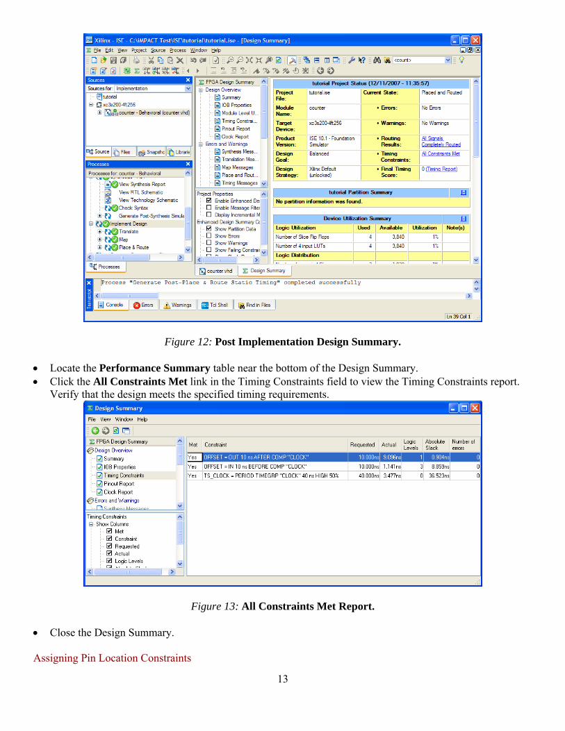
Figure 12: Post Implementation Design Summary. • Locate the Performance Summary table near the bottom of the Design Summary. • Click the All Constraints Met link in the Timing Constraints field to view the Timing Constraints report.
Verify that the design meets the specified timing requirements.
Figure 13: All Constraints Met Report. • Close the Design Summary. Assigning Pin Location Constraints

14
Specify the pin locations for the ports of the design so that they are connected correctly on the Spartan-3 Startup Kit demo board. To constrain the design ports to package pins, do the following: • Verify that counter is selected in the Sources window. • Double-click the Floorplan Area/IO/Logic - Post Synthesis process found in the User Constraints process
group. The Xilinx Pinout and Area Constraints Editor (PACE) opens. • Select the Package View tab. • In the Design Object List window, enter a pin location for each pin in the Loc column using the following
information: o CLOCK input port connects to FPGA pin P69 (CLK2 signal on board) o COUNT_OUT<0> output port connects to FPGA pin P5 (LD4 signal on board) o COUNT_OUT<1> output port connects to FPGA pin P4 (LD5 signal on board) o COUNT_OUT<2> output port connects to FPGA pin P3 (LD6 signal on board) o COUNT_OUT<3> output port connects to FPGA pin P2 (LD7 signal on board) o DIRECTION input port connects to FPGA pin P38 (SW0 signal on board)
Figure 14: Package Pin Locations. Notice that the assigned pin locations are shown in blue: • Select File → Save. • Close PACE. Notice that the Implement Design processes have an orange question mark next to them, indicating they are out-of-date with one or more of the design files. This is because the UCF file has been modified.

15
VIII. Reimplement Design and Verify Pin Locations Reimplement the design and verify that the ports of the counter design are routed to the package pins specified in the previous section. First, review the Pinout Report from the previous implementation by doing the following: • Open the Design Summary by double-clicking the View Design Summary process in the Processes window. • Select the Pinout Report and select the Signal Name column header to sort the signal names. Notice the
Pin Numbers assigned to the design ports in the absence of location constraints. • Reimplement the design by double-clicking the Implement Design process. • Select the Pinout Report again and select the Signal Name column header to sort the signal names. • Verify that signals are now being routed to the correct package pins. • Close the Design Summary.
Figure 15: Package Pin Locations Prior to Pin Location Constraints.
IX. Download Design to the Digilent Board This is the last step in the design verification process. This section provides simple instructions for downloading the counter design to the Spartan-3E Digilent board. • Connect the USB cable to the power input on the demo board. • Connect the download cable between the PC and demo board. • Select Implementation from the drop-down list in the Sources window. • Select counter in the Sources window. • In the Process window, double-click the Generate Programming File. • Open ExPort : Start-All programs-Digilent- Adept - ExPort
16
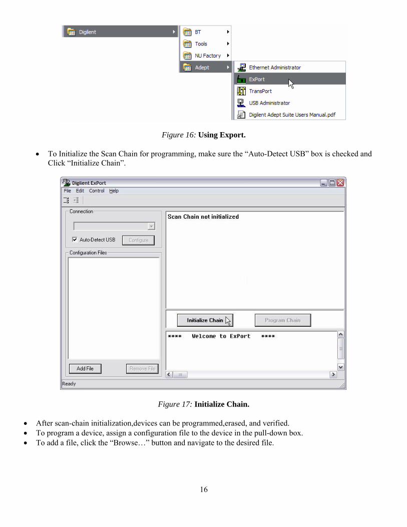
Figure 16: Using Export.
• To Initialize the Scan Chain for programming, make sure the “Auto-Detect USB” box is checked and Click “Initialize Chain”.
Figure 17: Initialize Chain.
• After scan-chain initialization,devices can be programmed,erased, and verified. • To program a device, assign a configuration file to the device in the pull-down box. • To add a file, click the “Browse…” button and navigate to the desired file.
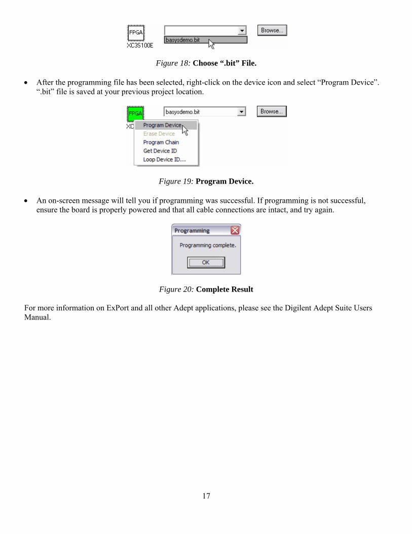
17
Figure 18: Choose “.bit” File. • After the programming file has been selected, right-click on the device icon and select “Program Device”.
“.bit” file is saved at your previous project location.
Figure 19: Program Device.
• An on-screen message will tell you if programming was successful. If programming is not successful, ensure the board is properly powered and that all cable connections are intact, and try again.
Figure 20: Complete Result
For more information on ExPort and all other Adept applications, please see the Digilent Adept Suite Users Manual.