overview - georgia institute of technologyweb.chemistry.gatech.edu/class/8873/semiconductor.pdf ·...
TRANSCRIPT

1
Overview:Inorganic semiconductors and semiconductordevices+ links to organic semiconductors
Why inorganic semiconductors ?
They are “electronic materials“ (at this time probably the mostimportant ones)
Very well established models• often they can be applied to conjugated materials
• sometimes they cannot
• and sometimes nobody knows so far
• materials of interest and their crystal-structures
• band-structures of inorganic (and organic) materials(gap energies, reciprocal space, effective mass, density of states …)
• optical properties of semiconductors
• semiconductor statistics and doping
• semiconductor-heterostructures
• p-n junctions
• light emitting devices and lasers
• photodetectors and solar cells
• field effect transistors

2
MaterialsInorganic semiconductors (usually crystalline)
from: S.M. Sze, “Semiconductor Devices, Physics and Technology“
n
n
Organic semiconductors (crystalline or amorphous; much bigger variety !)
poly(acetylene)
poly(para-phenylene)
n
SS
n
poly(para-phenylenevinylene)
poly(thiophene)
polymers
Oligomers and molecules (molecular crystals)
sexiphenyl
pentacene
aluminum tris(8-hydroxyquinoline) Alq3
Cu-phthalocyanine

3
Typical crystal-structures of inorganic semiconductors
S. M. Sze, “Physics of semiconductor devices“
crystal structure: basis vectors
all lattice sites can be defined by:
At each lettice point one finds the basis
Diamond: fcc with 2 C in basis
c,b,a���
cnbmalR����
++=
Zinc blende and wurzite lattice generated from
tetragonal building blocks
from Ch. Weißmantel and C. Hamann “Grundlagen der Festkörperphysik”
Zinc blende wurzite

4
S. M. Sze, “Physics of semiconductor devices“
Wurzite lattice (CdS, ZnS …..)
GaAs: face-centered cubic (fcc) lattice with GaAs in the basis�� �� two interpenetrating fcc lattices
CdS: two interpenetratinghexagonal close-pacced (hcp) lattices
Crystal-structures of molecular crystals and crystallineconjugated polymersVery different packing forces: to a significant extent dispersion forces (van der Waals) + electrostatic contributions
especially molecular crystals: often unit cells with a much lower symmetry
b
a
χ
c
bcrystal structure of p-terphenyl• monoclinic• herringbone• layered

5
Inorganic semiconductors – strong interaction in all 3 dimensions�� �� we NEED to describe them by a 3D bandstructure
Band-structures of semiconductors
Would be a 4D plot ???
Yu, Cardona, „Fundamentals of Semiconductors“
Reciprocal spacedefine reciprocal basis vectors:
In k-space (momentum-space), they play the same role, the basis vectorsplay in real space; (they define the “repeat-unit“ in k-space)
• perpendicular to the faces of the unit cell• length inversely proportional to that of the corresponding vector in real space�� �� reciprocal lattice, where every point can be expressed by:
( ) ( ) ( )cba
bac,
cba
acb,
cba
cba ***
���
���
���
���
���
���
××=
××=
××= πππ 222
*** clbkahG����
++=for Bloch-type wavefunctions one finds for the associated energies:
( )[ ] ( )[ ]rErEGkk
�����
+= ψψ

6
Unit cell in reciprocal space: 1st Brillouin zone
crystal structure: positions periodic in real space
band-structure: k-vectors “periodic“ in reciprocal space
S. M. Sze, “Physics of semiconductor devices“
S. M. Sze, “Physics of semiconductor devices“
Band-structures of “most important“ inorganic semiconductors

7
What can we easily see in the band-structure diagram:
• bandgap energy
• width of the bands
• number of bands
• effective mass (transport)
• direct vs. indirect gap (optical properties)
Different k-directions for bottom of the conduction band …(cannot be derived from symmetry arguments)
Shapes of constant energy surfaces in Ge, Si, and GaAs for the unoccupied bands
S. M. Sze, “Physics of semiconductor devices“
“simplified“ band-picture• k-dependence not explicitly considered• often very useful when discussing device
• shaded area denotes energy range, in which Bloch-states aseigenfunctions of the Schrödinger equation exist• x-axis: position !
S. M. Sze, “Physics of semiconductor devices“

8
Effective mass
Let‘s assume a free electron, which is described by:
Ψ=Ψ∆−=Ψ Em
H2
2�
�� �� eigenfunctions (plane waves):
energy eigenvalues:(energy-wavevector relations)
( ) rkier��� =Ψ
( )m
kkE
2
22�
��=
parabolic “band“
bands in semiconductors also (approximately) parabolic …..
(at least close to the band-edges)
let‘s define a “crystal electron“ with an effective mass m * so that the band structurecan be written as:
“crystal electron“ (QUASIPARTICLE) behaves like a free electron with mass m* !(indee the case, e.g., when applying a field)
How can we get m* from the actual band structure E(k) ?
( )*m
kkE
2
22�=
Hamaguchi, “Basic semiconductor physics“

9
Or for the more general 3D case (where m* is a second rank tensor)(in this way it also contains, e.g., anisotropic transport properties)
( )0
2
2
2
11
kk* dk
kEdm =
=�
( )0
2
2
11
kkjiij* kk
kEm
=∂∂
∂=�
�
The effect of the “surrounding“ (i.e., periodic lattice) is condensedinto the effective parameter m* !
approximation OK, for all future considerations in this course …
Density of statesSo far we know for which combination of k and E there exists an eigenstate …
Often it is sufficient to know, how many states exist between a certainenergy E and E+dE per unit volume V
(the derivation can be found in any standard solid-state physics textbook …)
3D extended system (i.e., bulk semiconductors):
for E > Ec in the case of conduction band statesand E < Ev for valence band states
• increases with increasing m*• square-root dependence on E
( ) V,C
*
EEm
Eg −���
����
�=
23
22
22
1�π
g(E)
10
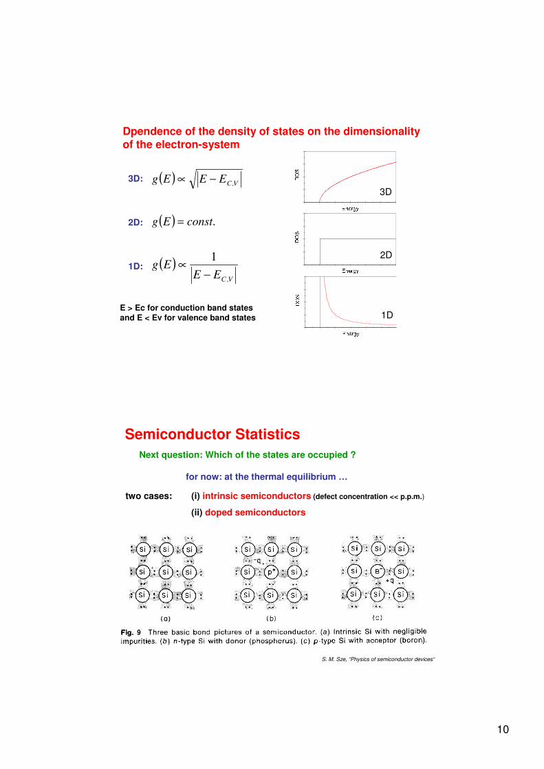
Dpendence of the density of states on the dimensionalityof the electron-system
3D:
2D:
1D:
E > Ec for conduction band statesand E < Ev for valence band states
( ) V,CEEEg −∝
( ) .constEg =
( )V,CEE
Eg−
∝ 1
3D������ ��
� �
1D
2D������ ��
� �
������ ��
� �
Semiconductor StatisticsNext question: Which of the states are occupied ?
for now: at the thermal equilibrium …
two cases: (i) intrinsic semiconductors (defect concentration << p.p.m.)
(ii) doped semiconductors
S. M. Sze, “Physics of semiconductor devices“

11
Fermi-Dirac distribution function(probability for a Fermion state – here an electron or hole state – to be occupied)
EF … Fermi-Energy (only“adjustable“ parameter)
( )���
����
� −+
=
TkEE
exp
EF
B
F1
1
Note: probability F istemperature-dependent !!!
-0.3 -0.2 -0.1 0.0 0.1 0.2 0.3
0.0
0.2
0.4
0.6
0.8
1.0
����� � �������
�
���� � �! �#" �$#%�& �
Approximations:(E-EF) > 3 kBT
(E-EF) < -3 kBT
i.e., Fermi-level deeplyinside the gap
( ) ���
����
� −−≈TkEE
expEFB
F
( ) ���
����
� −−−≈
TkEE
expEFB
F1
Number of electrons in the conduction band (per unit volume):
( ) ( )�=top
C
E
EC dEEFEgn
inserting the expressions for g(E) and F(E) this becomes:
����
����
� −+
���
����
�=
top
C
E
E
B
F
//
B*
dE
TkEE
exp
ETkmn
1
22
1 2123
22�π
Looks complicated – and in the general case does not have an analyticsolution ����
BUT: we can find a solution for the approximate case mentioned before(„EF is far enough away from the band-edges !“)

12
In this case: number of electrons in the conduction band
Exponential decrease of the number of electrons in the conductionband with the „distance“ of the Fermi-level from the band-edge !
equivalently for the number of holes in the valenece band:
== number of electron states that are NOT occupied
23
222
/
Be*
CB
FCC
TkmNwith
TkEE
expNn ���
����
�=��
�
����
� −−≈
�π
23
222
/
Bh*
VB
VFV
TkmNwith
TkEE
expNp ���
����
�=��
�
����
� −−≈
�πNC and NV are called the effective densities of states in the conduction and valence bands
���
����
� −−=��
�
����
� −−��
�
����
� −−=
TkEE
expNNTkEE
expTkEE
expNNnpB
VCVC
B
VF
B
FCVC
or:
The product of p and n depends only on the material (EG, me*, mh*) and on temperature. It is independent of doping !
If n is increase by n-type doping, p has do decrease accordingly and vice versa !
���
����
�−=
TkE
expNNnpB
GVC

13
Intrinsic semiconductors:
inpn ≡=ni … intrinsic carrier density
Continous thermal excitations of electrons from the VB into the CBIn thermodynamic equilibrium: balanced by carrier recombination …
Where is the Fermi level in an intrinsic semiconductor ?
from n = p:
At 0K, EF is in the middle of the gap of an intrinsic semiconductor !
���
����
�−==
TkE
expNNnpnB
GVCi 2
���
����
�+
+=
e*
h*
BVCF m
mln
TkEEE
43
2
Simplified BS
Density of states (DOS)
Fermi-Dirac distribution
S. M. Sze, “Physics of semiconductor devices“
Carrier density

14
Doped Semiconductors
donor-level: neutral if filled by an electron and positive if emptyacceptor-level: neutral if filled by an electron and positive if empty
There are deep and shallow donors and acceptors.
from: S.M. Sze, “Semiconductor Devices, Physics and Technology“
from: S.M. Sze, “Semiconductor Devices, Physics and Technology“

15
Qualitatively:
donors increase n and consequentlydecrease p
acceptorsincrease p and consequentlydecrease n
S. M. Sze, “Physics of semiconductor devices“
Quantitative description:
add dopands (typically 1012 to 1018 cm-3)'' '' EF has to adjust to preserve charge neutrality
(reasonable) assumption for shallow dopands: all ionized !
donors with density ND: n=ND
or
acceptors with density NA: p=NA
Doping with donors: EF approaches the conduction band edge EC
Doping with acceptors: EF approaches the valence band edge EV
���
����
�−=
D
CBCF N
NlnTkEE
���
����
�−=
A
VBVF N
NlnTkEE

16
At low temperatures the complete ionization approximation does not apply!
Charge neutrality:
At very high temperatures intrinsic effects start to dominate !
+− +=+ DA NpNn
S. M. Sze, “Physics of semiconductor devices“
Optical properties of semiconductors
Energy- and momentumconservation !
Rosencher and Vinter, “Optoelectronics“

17
Comparison of Si and GaAsE
nerg
y(e
V)
S. M. Sze, “Physics of semiconductor devices“
direct excitations indirect excitations
Indirect excitations
simultaneous absorption of a photon and generation or annihilation of a phonon
(( (( very improbable process (3-particle process) !(( (( small associated absorption coefficient !(( (( vanishingly small emission probability !
Silicon can be (and is) used in solar cells but not in LEDsand lasers (only in combination with color centers)

18
Absorption coefficient of Ge as a function of temperature
G.G. Macfarlane et al, Phys. Rev. 108, 1377 (1957)
Direct (vertical) absorption
For the absorption process to happen there needs to be a filled state in the conduction band and an empty state in the valence band !
absorption coefficient proportional to the corresponding density of states !
( ) Geff Eg −���
����
�= ω
µπ
ω ��
�
23
22
2
21 with
h*
e*
eff mm111 +=
µ���� joint density of states
GE−∝ ωα �

19
Excitonic effects
Experimental spectrum for GaAs:
Absorption coefficient of GaAs as a function of temperature
M. D. Struge, Phys. Rev. 127, 768 (1962)
Not “exactly“ E1/2 dependence !
Reason for the abrupt onset of the absorption and peak: excitonic effects
So far: electron is excited from state in VB to a state in the CB
BUT (even if we stay within a single-particle picture):
Interaction between the positively charged hole and thenegatively charged electron
bound electron-hole pair = exciton
Most simple description: treated like H-atom withand �r of the medium
h*
e*
eff mm111 +=
µ
GaAs: µeff very small and �r )) )) 13 EB )) )) 4 meV r1S )) )) 300 Å