outline - university of notre dame
TRANSCRIPT

1
CMOS VLSI Design
Introduction toCMOS VLSI
Design
Power
Peter KoggeUniversity of Notre Dame
Fall 2012
Based on lecture slides by Jay Brockman & David Harris
http://www.cmosvlsi.com/coursematerials.html
Slide 1Power
CMOS VLSI Design Slide 2Power Slide 2
Outline Motivation
Thermal Resistance
Energy 101
Dynamic Power
Static Power
Low Power Design
Historical Trends

2
CMOS VLSI Design Slide 3Power Slide 3
Power and Energy (Chap 5)
Energy = ability to do work – in Joules – watts*seconds
Power = rate at which work performed or energy converted
– CMOS: drawn from VDD pin(s) of a chip, & converted to heat
– in units of Watts – volts*amps
Instantaneous Power:
Energy:
Average Power:
( ) ( )DD DDP t i t V
0 0
( ) ( )T T
DD DDE P t dt i t V dt
avg
0
1( )
T
DD DD
EP i t V dt
T T
Power
CMOS VLSI Design Slide 4
Getting A Feel for the Units
Joules (J) are “Watt-seconds” = “Volts*Amps”
– Relevant CMOS Unit: 1 picoJoule (pJ) = 10-12 J
Consider a typical cell phone (Motorola RAZR V3)
– Battery: 3.6 V, 680mA Hours: Stored Energy:
• = 3.6V * 0.68A Hr * 3600sec/Hr
• = 8812.8 Watt-secs = 8812.8 Joules = 8.8x10¹⁵ pJ
– Continuous talk time: 200-430 minutes
• 430 min = 25,800 seconds
So while talking, cell draws (8812.8/25800) = 0.34 Watts
– or 0.34 J to talk 1 second
– or 1 pJ can run cell phone for 2.94 picoseconds
Power
3
CMOS VLSI Design
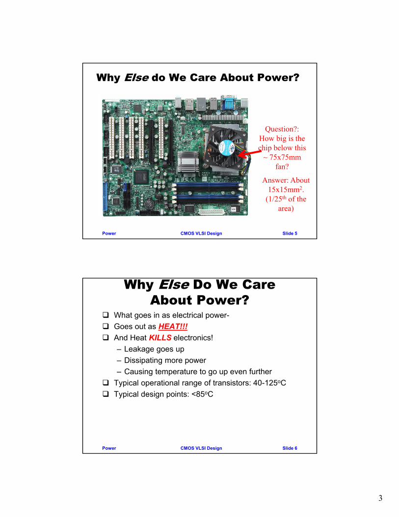
Why Else do We Care About Power?
Power Slide 5
Question?: How big is the chip below this
~ 75x75mm fan?
Answer: About 15x15mm2.
(1/25th of the area)
CMOS VLSI Design
Why Else Do We Care About Power?
What goes in as electrical power-
Goes out as HEAT!!!
And Heat KILLS electronics!
– Leakage goes up
– Dissipating more power
– Causing temperature to go up even further
Typical operational range of transistors: 40-125oC
Typical design points: <85oC
Power Slide 6

4
CMOS VLSI Design
Thermal Resistance
Thermal Resistance: Steady state temperature difference between two endpoints per watt dissipated in source.
– Depends on material and shape of object conducting heat
– Units: oC/W
For complex thermal path, obeys laws similar to resistance
– Series paths increase thermal resistance
– Parallel paths reduce thermal resistance
In electronics, a function of
– How chip is packaged
– Heat Sink to airPower Slide 7
Free Air:Nominally 30oC
ThermalResistance
Heat flow
Heat Source(a transistor)
CMOS VLSI Design
Key Definitions Q: power dissipated by device
TJ: temperature of a transistor “junction” in the device
TJMAX: maximum operating temperature of a transistor “junction” in the device
TC: temperature of the case
TH: temperature of the heatsink
TAMB: temperature of the air
∆Tij: difference in temperature between points I and j
RθJC: thermal resistance from junction to case
RθCH: thermal resistance from case to heatsink
RθHA: thermal resistance from heatsink to air
Power Slide 8
Term Typical
TJMAX 125oC
TAMB 70oC
RθJC 1.5oK/W
RθHA 4oK/W
RθB (heat transfer Pad)
0.1oK/W
http://en.wikipedia.org/wiki/Thermal_resistance

5
CMOS VLSI Design
Equations ∆T = Q x Rθ
Rθ = RθJC + RθCH + RθHA
∆T = TJMAX - TAMB
Solving for Q:
– Qmax = (TJMAX – TAMB)/(RθJC + RθCH + RθHA)
Using prior numbers for a TO-220 case:
– Qmax = (125 – 70) /(1.5 +0.1 +4) = 9.8W
Power Slide 9
CMOS VLSI Design
How Do We Do Better? Place chip as close as
possible to metal shell
Adding more surface area to Heat Sink adds more paths for heat escape
– Add “fins”
Don’t let air sit over heat sink
– Blow cool air to reduce “ambient”
Net Result: we can cheaply air cool ~ 130W per chip
More requires liquid cooling
Power Slide 10

6
CMOS VLSI Design
How About REALCompute Power?
Power Slide 11
CMOS VLSI Design Slide 12
Moore’s Law 1965, Gordon Moore: “the number of transistors that can be
integrated on a die would double every 18 to 14 months.”
– Equivalent to Feature Size decreasing by factor of √2
– Memory density 4X every 3 years
0
0
1
10
100
1,000
10,000
1975 1980 1985 1990 1995 2000 2005 2010 2015 2020
Tra
nsi
sto
r C
ou
nt
(Mil
lio
ns)
Historical Single Core Historical Multi-Core ITRS Projections
64
256
1,000
4,000
16,000
64,000
256,000
1,000,000
4,000,000
16,000,000
64,000,000
10
100
1000
10000
100000
1000000
10000000
100000000
1980 1983 1986 1989 1992 1995 1998 2001 2004 2007 2010
Year
Kb
it c
apac
ity/
chip
1.6-2.4 m
1.0-1.2 m
0.7-0.8 m
0.5-0.6 m
0.35-0.4 m
0.18-0.25 m
0.13 m
0.1 m
0.07 m
human memoryhuman DNA
encyclopedia2 hrs CD audio
30 sec HDTV
book
page
4X growth every 3 years!
Power

7
CMOS VLSI Design Slide 13
Smaller Feature Sizes Also Enable Higher Clock Rates
10
100
1,000
10,000
100,000
1975 1980 1985 1990 1995 2000 2005 2010 2015 2020
Clo
ck
(M
Hz)
Historical ITRS Max Clock Rate (12 invertors)
10
100
1000
10000
100000
10100100010000
Feature Size
Clo
ck (
MH
z)
Historical ITRS Max
3 GHz
2005 projection was for 5.2 GHz – and we didn’t make it.Further, we’re still stuck at 3+GHz in production.
3 GHz
Power
CMOS VLSI Design Slide 14
Why the Clock Flattening? POWER
1
10
100
1000
1976 1986 1996 2006
Wat
ts p
er D
ie
0.1
1
10
100
1000
1976 1986 1996 2006
Wat
ts p
er S
qu
are
cm
Hot, Hot, Hot!
Light Bulb
Iron
Rocket Nozzle
Power

8
CMOS VLSI Design
CMOS Energy 101
Power Slide 15
CMOS VLSI Design Slide 16
CMOS Energy 101
Vin Vg
R & C C
0
0.2
0.4
0.6
0.8
1
1.2
0 5 10 15 20
Vo
ltag
e
Vin
Vg
Dissipate CV2/2And store CV2/2
Dissipate CV2/2From Capacitance
One clock cycle dissipates C*V2
Power

9
CMOS VLSI Design Slide 17
How Did CV2 Improve With Time?
10
100
1000
1985 1990 1995 2000 2005 2010 2015 2020 2025
Fea
ture
Siz
e
Assume capacitance of a circuitscales as feature size
0.01
0.10
1.00
10.00
100.00
1000.00
1/1/
88
1/1/
90
1/1/
92
1/1/
94
1/1/
96
1/1/
98
1/1/
00
1/1/
02
1/1/
04
1/1/
06
1/1/
08
1/1/
10
1/1/
12
1/1/
14
1/1/
16
1/1/
18
1/1/
20
1/1/
22
1/1/
24
CV
^2 r
elat
ive
to 9
0nm
Hi P
erf
Lo
gic
High Perf Logic Low Operating Pow er Logic Memory Process
330X
15X
90nm picked as breakpoint because that’s when Vdd and thus clocks flattened
0
1
2
3
4
5
6
1970 1980 1990 2000 2010 2020
Vd
d
Power
CMOS VLSI Design Slide 18
Total CMOS PowerStatic Dissipation
“Always there”
Subthreshold conduction thru OFF transistors
Tunneling thru oxide
Leakage thru reverse biased diodes
Contention current in ratioed logic
Dynamic Dissipation
Power dissipated only at specific times
Charging & Discharging of load capacitances
“Short circuit” when both p and n types partially on
Ptotal = Pdynamic + Pstatic
Power

10
CMOS VLSI Design
Dynamic Power
Power Slide 19
CMOS VLSI Design Slide 20Power Slide 20
Dynamic Power I Charge & discharge load capacitances when
transistors switch.
One cycle involves a rising and falling output.
On rising output, charge Q = CVDD is required
On falling output, charge is dumped to GND
This repeats Tfsw times
over an interval of T
Cfsw
iDD(t)
VDD
Remember: Current = charge/time

11
CMOS VLSI Design Slide 21Power
CMOS VLSI Design Slide 22Power Slide 22
Dynamic Power II When transistors switch, both nMOS and pMOS
networks may be momentarily ON at once
Leads to a blip of “short circuit” current.
– Also called Crowbar current
< 10% of dynamic power if rise/fall times are comparable for input and output

12
CMOS VLSI Design Slide 23Power
CMOS VLSI Design Slide 24Power Slide 24
Dynamic Power Cont.
Cfsw
iDD(t)
VDD
dynamic
0
0
sw
2sw
1( )
( )
T
DD DD
TDD
DD
DDDD
DD
P i t V dtT
Vi t dt
T
VTf CV
T
CV f
Charge in 1 cycle
# of cycles in T time
Integral of i is total charge converted
Remember this Equation

13
CMOS VLSI Design Slide 25Power Slide 25
Activity Factor Not all gates switch every cycle
Suppose the system clock frequency = f
Let fsw = f, where = activity factor
– If the signal is a clock, = 1
– If the signal switches once per cycle, = ½
– Dynamic gates:
• Switch either 0 or 2 times per cycle, = ½
– Static gates:
• Depends on design, but typically = 0.1
Revised Dynamic power:2
dynamic DDP CV f
CMOS VLSI Design Slide 26
7: Power 14CMOS VLSI DesignCMOS VLSI Design 4th Ed.
Activity Factor Estimation Let Pi = Prob(node i = 1)
– Pi = 1-Pi
i = Pi * Pi
Completely random data has P = 0.5 and = 0.25
Data is often not completely random
– e.g. upper bits of 64-bit words representing bank account balances are usually 0
Data propagating through ANDs and ORs has lower activity factor
– Depends on design, but typically ≈ 0.1
Power

14
CMOS VLSI Design Slide 27Power
CMOS VLSI Design Slide 28Power

15
CMOS VLSI Design Slide 29
7: Power 11CMOS VLSI DesignCMOS VLSI Design 4th Ed.
Dynamic Power Example 1 billion transistor chip
– 50M logic transistors• Average width: 12 • Activity factor = 0.1
– 950M memory transistors• Average width: 4 • Activity factor = 0.02
– 1.0 V 65 nm process– C = 1 fF/m (gate) + 0.8 fF/m (diffusion)
Estimate dynamic power consumption @ 1 GHz. Neglect wire capacitance and short-circuit current.
Power
(with λ = 25nm)
CMOS VLSI Design Slide 30
7: Power 12CMOS VLSI DesignCMOS VLSI Design 4th Ed.
Solution
6logic
6mem
2
dynamic logic mem
50 10 12 0.025 / 1.8 / 27 nF
950 10 4 0.025 / 1.8 / 171 nF
0.1 0.02 1.0 1.0 GHz 6.1 W
C m fF m
C m fF m
P C C
Power

16
CMOS VLSI Design
Static Power
Power Slide 31
CMOS VLSI Design Slide 32Power Slide 32
Static Power (5.3) Static power is consumed even when chip is quiescent.
Leakage draws power from “nominally” OFF devices:
– Pstatic = IstaticVdd
Two forms of leakage current:
– Subthreshold Leakage: conduction thru OFF transistors
– Gate Leakage: conduction across transistor gates when transistor is on
Both proportional to total widths of transistors in on and off states, AND thresholds of transistors
– Low Threshold Transistors: turn on fast but leak more
– High Threshold Transistors: slower, but leak much less
Power

17
CMOS VLSI Design Slide 33Power Slide 33
Leakage Example 200 Million transistor chip
– 20M logic transistors ave width: 12 – 180M memory transistors ave width: 4
1.2 V 100 nm processµm
On average 50% of Transistors OFF 2 types of transistors
– “Low-threshold”/Hi Leakage• Fast but leaky• Used in 20% of logic• Gate leakage = 3nA/µm• Subthreshold leakage for OFF =
20nA/µm– “High threshold”/Low Leakage
• Slow but less leakage• In All Memory & 80% logic• Gate leakage = 0.002nA/µm• Subthreshold leakage for OFF =
0.02nA/µm
Estimate static power Compute µm of hi leakage transistors
– 20Mx20% x 12λ x 0.05µm – = 2.4x106 µm
Compute µm of low leakage transistors– 20Mx80% x 12λ x 0.05µm – + 180M x 4λ x 0.05µm – = 45.6x106 µm
Gate leakage– Hi: 2.4x106 µm 50% x 3nA/µm =
3.6mA– Low: 45.6x106 µm x 50%
0.002nA/µm = 0.045mA Subthreshold leakage
– Hi: 2.4x106 µm x 50% x 20nA/µm = 24mA
– Low: 45.6x106 µm x 50% x 0.02nA/µm = 0.456mA
Total Current = 28.1 mA At 1.2V this is 34mW
CMOS VLSI Design Slide 34Power Slide 34
Redo with No Low Leakage Devices
200 Million transistor chip– 20M logic transistors ave width: 12
– 180M memory transistors ave
width: 4 1.2 V 100 nm process
µm 2 types of transistors
– “Low-threshold”/Hi Leakage • Used in 20% of logic• Gate leakage = 3nA/µm• Subthreshold leakage for OFF
= 20nA/µm– “High threshold”/Low Leakage
• in Memory & 80% logic• Gate leakage = 0.002nA/µm• Subthreshold leakage for OFF
= 0.02nA/µm All transistors have gate leakage On average 50% of Transistors OFF
Estimate static power Total µm of transistors
– 2.4x106 µm + 45.6x106 µm– = 48x106 µm
Gate leakage– 48x106 µm x 50% 3nA/µm =
72mA Subthreshold leakage
– 48x106 µm x 50% x 20nA/µm = 480mA
Total Current = 552mA At 1.2V this is 662 mW
This is 20X MORE power
Power

18
CMOS VLSI Design
Power Reduction Techniques
Power Slide 35
CMOS VLSI Design Slide 36
Modern Terminology Energy Delay Product
– Notionally: • “Energy used to perform some function”• times “Time required to do function”
– Many variants Dynamic Clock and Voltage Scaling
– Under periods of light loads, reduce clock– And if possible reduce Vdd to point where clock is
“max possible” Clock Gating
– In pipelined systems gating the clocks to latches off when circuits are not in use
Power

19
CMOS VLSI Design Slide 37Power Slide 37
Low Power Design Reduce dynamic power
– : clock gating, sleep mode
– C: small transistors (esp. on clock), short wires
– VDD: lowest suitable voltage
– f: lowest suitable frequency
Reduce static power
– Selectively use low Vt devices
– Leakage reduction:
stacked devices, body bias, low temperature
CMOS VLSI Design Slide 38
Example Technique: Intel “Speedstep”
As we decrease clock rate, we can also reduce voltage
Significant example: Pentium M– cf: ftp://download.intel.com/design/network/papers/30117401.pdf
F Vdd fV^2 Ref f Rel fV^21.6 1.484 3.52 1.00 1.001.4 1.420 2.82 0.88 0.801.2 1.276 1.95 0.75 0.551.0 1.164 1.35 0.63 0.380.8 1.036 0.86 0.50 0.240.6 0.956 0.55 0.38 0.16
0.00
0.10
0.20
0.30
0.40
0.50
0.60
0.70
0.80
0.90
1.00
0.00 0.20 0.40 0.60 0.80 1.00
Relative Clock Rate
Rel
ativ
e P
ow
er
6:1 ratio in power
3:1 ratio in speed
If capacitance remained ConstantIn reality (include leakage etc)
Power

20
CMOS VLSI Design Slide 39
7: Power 25CMOS VLSI DesignCMOS VLSI Design 4th Ed.
Leakage Control Leakage and delay trade off
– Aim for low leakage in sleep and low delay in active mode
To reduce leakage:– Increase Vt: multiple Vt
• Use low Vt only in critical circuits– Increase Vs: stack effect
• Input vector control in sleep– Decrease Vb
• Reverse body bias in sleep• Or forward body bias in active mode
Power
Also: for series transistors, keep normally off signals at bottom
CMOS VLSI Design Slide 40
7: Power 27CMOS VLSI DesignCMOS VLSI Design 4th Ed.
NAND3 Leakage Example 100 nm process
Ign = 6.3 nA Igp = 0
Ioffn = 5.63 nA Ioffp = 9.3 nA
Data from [Lee03]
Power

21
CMOS VLSI Design Slide 41
7: Power 29CMOS VLSI DesignCMOS VLSI Design 4th Ed.
Power Gating Turn OFF power to blocks when they are idle to
save leakage– Use virtual VDD (VDDV)– Gate outputs to prevent
invalid logic levels to next block
Voltage drop across sleep transistor degrades performance during normal operation– Size the transistor wide enough to minimize
impact Switching wide sleep transistor costs dynamic power
– Only justified when circuit sleeps long enough
Power
CMOS VLSI Design Slide 42
What About “Sleep States?”
from ATOM chip documentation page http://download.intel.com/design/processor/datashts/319535.pdf
StopGrant
Normal Sleep DeepSleep
DeeperSleep
StopGrantSnoop
• Stop Grant: Threads stop executing, but clocks running• Sleep:
•Caches maintained •PLL maintained•Internal clocks stopped•Will respond to interrupts/snoops
•Deep Sleep•Will NOT respond to interrupts/snoops
•Deeper Sleep•L2 cache emptied•Vdd lowered even further
Power