outline - college of william & mary
TRANSCRIPT

OutlineOutline
1. DSP project info
2. Analog-to-digital converters
3. Digital-to-analog converters
4. 2-dimensional register memory

DSP ProjectDSP Project
Reminder:Reminder: Project proposal is due Friday, October 26, 2007 by 5pm5pm.
Modification of technical specs of lockModification of technical specs of lock--in amplifier:in amplifier:
Phase control: 0 to 360° with a resolution of at least 3.6°.
You must be able to shift the phase by exactly 90° from any phase position.
Basic guideline for project proposal Basic guideline for project proposal (also see (also see Project GuidelinesProject Guidelines document)document)::
You must convince your reader that your design concept will work well enough that it deserves to be funded. This means that your design has reached the point that you can draw up a budget. Your proposal must include a budget which is as Your proposal must include a budget which is as specific as possible specific as possible and an expected timeline.and an expected timeline.

Analog Analog DigitalDigital
As physicists, we know that:
We live in an analoganalog world of continuously varying signals.
Almost all physical quantities (observables) are continuous in nature.
As electronics designers, we know that:
Digital electronics is very powerfulpowerful, cheapcheap, and relatively easyeasyto design (at least compared to analog circuits).
Digital electronics only works with digital signals.
THEREFORE …
If we’re ever going to make anything useful, we need to a way to convert (or approximate) an ANALOG signal to (by) a sequence of digital-binary numbers, and vice versa.

Analog Analog DigitalDigital
time
volts
3-bit digital approximation
Algorithm:Algorithm: At each clock cycle, round your analog voltage to the nearest digital value.
The size of a digital step is defined by Vref/2n for an n-bit converter.

ShannonShannon--NyquistNyquist Sampling TheoremSampling Theorem
THEOREM:THEOREM:
A continuous-time finite bandwidth signal can be exactly reconstructed from its samples if the sampling frequency is greater than 2 times the signal bandwidth B, where B is largest (non-zero) frequency component of the signal.
F=2B is referred to as the Nyquist frequency (the lowest possible sampling frequency).
Practical Considerations:Practical Considerations:
Any finite duration signal has B + ∞, so exact mathematical application of the theorem is impossible.
The theorem indicates the frequency scale that one should use in order to usefully sample a signal always use a sampling rate which is greater than always use a sampling rate which is greater than twice the highest frequency component of twice the highest frequency component of ““reasonable amplitudereasonable amplitude””..

Flash ADCsFlash ADCs
+–+–+–
+–+–+–
+–+–+–
+–+–+–
+–+–+–
+–+–+–
+–+–+–
VREF
Vin
3-bitencoder
bit-0
bit-1
bit-2
R
R
R
R
R
R
R
R
+–+–+–+–+–+–
+–+–+–+–+–+–
+–+–+–+–+–+–
+–+–+–+–+–+–
+–+–+–+–+–+–
+–+–+–+–+–+–
+–+–+–+–+–+–
VREF
Vin
3-bitencoder
bit-0
bit-1
bit-2
R
R
R
R
R
R
R
RThe fastest (and most expensive) n-bit ADCs use 2n-1 comparators to determine which of the 2n numbers the analog input is closest to.
8-bit ADC: 255 comparators.
12-bit ADC: 4096 comparators
In general, higher the bit resolution results in a slower ADC (and more expensive).
Most digital oscilloscopes use an 8-bit ADC.

ADC0820: HalfADC0820: Half--Flash ADC (I)Flash ADC (I)
In order to keep the number of comparators small, it holds the input voltage, and converts it in steps:
Converts the upper four bits with a 4-bit ADC.Converts the digitized value back into an analog value with a
Digital-to-Analog Converter (DAC).Subtracts this from the input to generate the smaller, difference
voltage.Finally, it uses a 2nd 4-bit ADC to convert the lower 4-bits.
The entire process takes less than 800 ns when operating off the internal timing of the ADC0820 (RD mode).
You can run it somewhat faster with some clever timing (WR-RD) mode but we will opt for simplicity.

[figure from the National Semiconductor ADC0820 datasheet]
ADC0820: HalfADC0820: Half--Flash ADC (II)Flash ADC (II)

ADC0820: HalfADC0820: Half--Flash ADC (III)Flash ADC (III)
Overflow—If the analog input is higher than the VREF(+), OFL will be LOW at the end of conversion. Can be used to cascade.
OFL 18
TRI-STATE data output—bits 4-7DB4-7 14-17
CS must be low for the RD or WR to be recognized.CS 13
Top of resistor ladder; range: VREF(−)≤VREF(+)≤VCCVREF(+)12
Bottom of resistor ladder; range: GND≤VREF(−)≤VREF(+) VREF(−)11
INT going LOW indicates that the conversion is completed and the data result is in the output latch. INT is reset by rising edge on RD or CS.
INT 9
WR-RD ModeWith CS low, the TRI-STATE data outputs (DB0-DB7) will be activated when RD goes low. RD ModeWith CS low, the conversion will start with RD going LOW; also RD will enable the TRI-STATE data outputs at the completion of the conversion. RDY going TRI-STATE and INT going low indicates the completion of the conversion.
RD 8
Select mode: LOW = RD Mode HIGH = WR-RD ModeMODE7
WR-RD Mode - WR: With CS low, the conversion is started on the falling edge of WR. RD Mode - RDY: RDY will go low after the falling edge of CS; RDY will go TRI-STATE when the result of the conversion is strobed into the output latch.
WR / RDY6
TRI-STATE data outputs; bit 0 (LSB) to bit 3DB0-DB3 2-5
Analog input; range GND ≤ VIN ≤ VCCVIN 1
FunctionName Pin
Functional TableFunctional Table

[figure from the National Semiconductor ADC0820 datasheet]
ADC0820: HalfADC0820: Half--Flash ADC (IV)Flash ADC (IV)
In RD mode, the RD# line going LOW initiates the conversion.
When the conversion is complete, the INT# line goes LOW & the data is latched into output buffers.
The output buffers will be put in a Z state when RDY# goes LOW until the INT# line goes LOW.

[figure from the National Semiconductor ADC0820 datasheet]
ADC0820: HalfADC0820: Half--Flash ADC (IV)Flash ADC (IV)
Keep CS low permanently
not important
These lines are IMPORTANT
In RD mode, the RD# line going LOW initiates the conversion.
When the conversion is complete, the INT# line goes LOW & the data is latched into output buffers.
The output buffers will be put in a Z state when WR# goes LOW until the INT# line goes LOW.

Digital Digital AnalogAnalog
A Digital-to-Analog Converter (DAC) is used to convert a digital signal into an analog voltage.
A DAC is useful for:A DAC is useful for:
Generating a voltage from a computer, microprocessor, or FPGA that will then control part of an experiment.
Producing a digitally synthesized waveform (triangle, sine, ormore complex).
Converting digital music to sound, etc …
(the CD standard is 16-bits at 44.1 KHz)
DACs are generally much faster than ADCs for a same bit resolution.

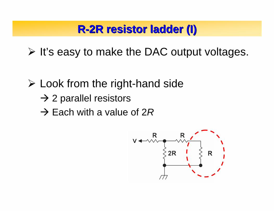
RR--2R resistor ladder (I)2R resistor ladder (I)
It’s easy to make the DAC output voltages.
Look from the right-hand side2 parallel resistorsEach with a value of 2R
R
RR--2R resistor ladder (I)2R resistor ladder (I)
It’s easy to make the DAC output voltages.
Look from the right-hand side2 parallel resistorsEach with a value of 2R
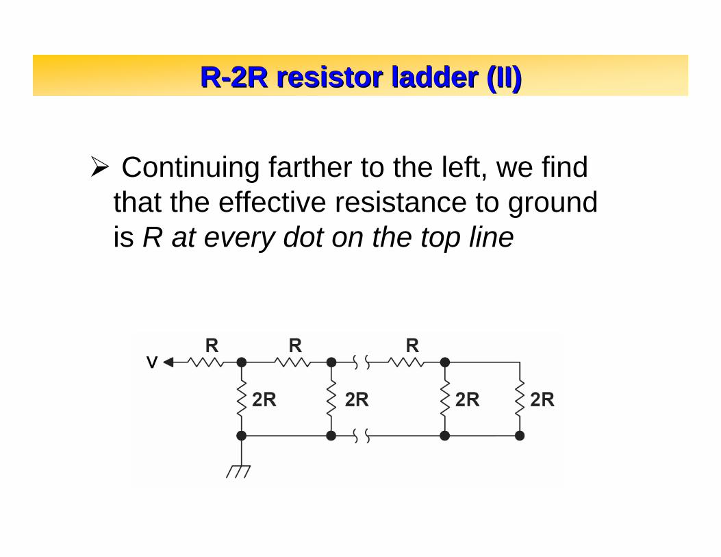
Continuing farther to the left, we find that the effective resistance to ground is R at every dot on the top line
RR--2R resistor ladder (II)2R resistor ladder (II)

The ladder acts like a series of voltage dividers that reduces the voltage by an additional factor of 2 at each R-2R junction.V decreases by half at each connection point
along the top rail.Thus each output voltage is related to the
input voltage by a power of two.
RR--2R resistor ladder (III)2R resistor ladder (III)

Simple DACSimple DAC
We can generate an analog voltage by adding together the voltages represented by the various stages in the ladder.If we sum the ladder outputs based on a simple a binary representation in switches then we have a DAC.
[figure from the Art of Electronics (2nd edition, 1999) by P. Horowitz and W. Hill, p. 616]
V V/2 V/4 V/8
Voltagesumming amplifier

Simple DACSimple DAC
We can generate an analog voltage by adding together the voltages represented by the various stages in the ladder.If we sum the ladder outputs based on a simple a binary representation in switches then we have a DAC.
[figure from the Art of Electronics (2nd edition, 1999) by P. Horowitz and W. Hill, p. 616]
V V/2 V/4 V/8
Current-to-Voltagesumming amplifier
I I/2 I/4 I/8

8-bit DAC (TLC7524)
A real DAC: the TLC7524A real DAC: the TLC7524
[figure from Texas Instruments TLC7524 datasheet]

TLC7524 timingTLC7524 timing
[figure from Texas Instruments TLC7524 datasheet]
Keep CS low permanently
The data on the digital inputs is sent to the analog output when WR goes LOW.
When WR is HIGH, the digital inputs and analog output remain latched to their present values.

ADC DAC8 Bits Out
ADC ADC DAC DAC AnalogAnalog--toto--AnalogAnalog
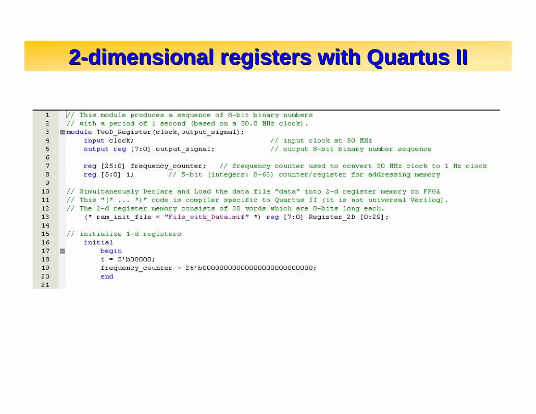
22--dimensional registers with dimensional registers with QuartusQuartus IIII

22--dimensional registers with dimensional registers with QuartusQuartus IIII
Declare 2Declare 2--d registerd register&&
Initialize with data in file.Initialize with data in file.

Using a 2Using a 2--d Register in d Register in VerilogVerilog

Using a 2Using a 2--d Register in d Register in VerilogVerilog
Reads the 8Reads the 8--bit word at address bit word at address ““ii”” of of ““Register_2DRegister_2D””&&
sends it to the 8sends it to the 8--bit 1bit 1--d register d register ““output_signaloutput_signal””..
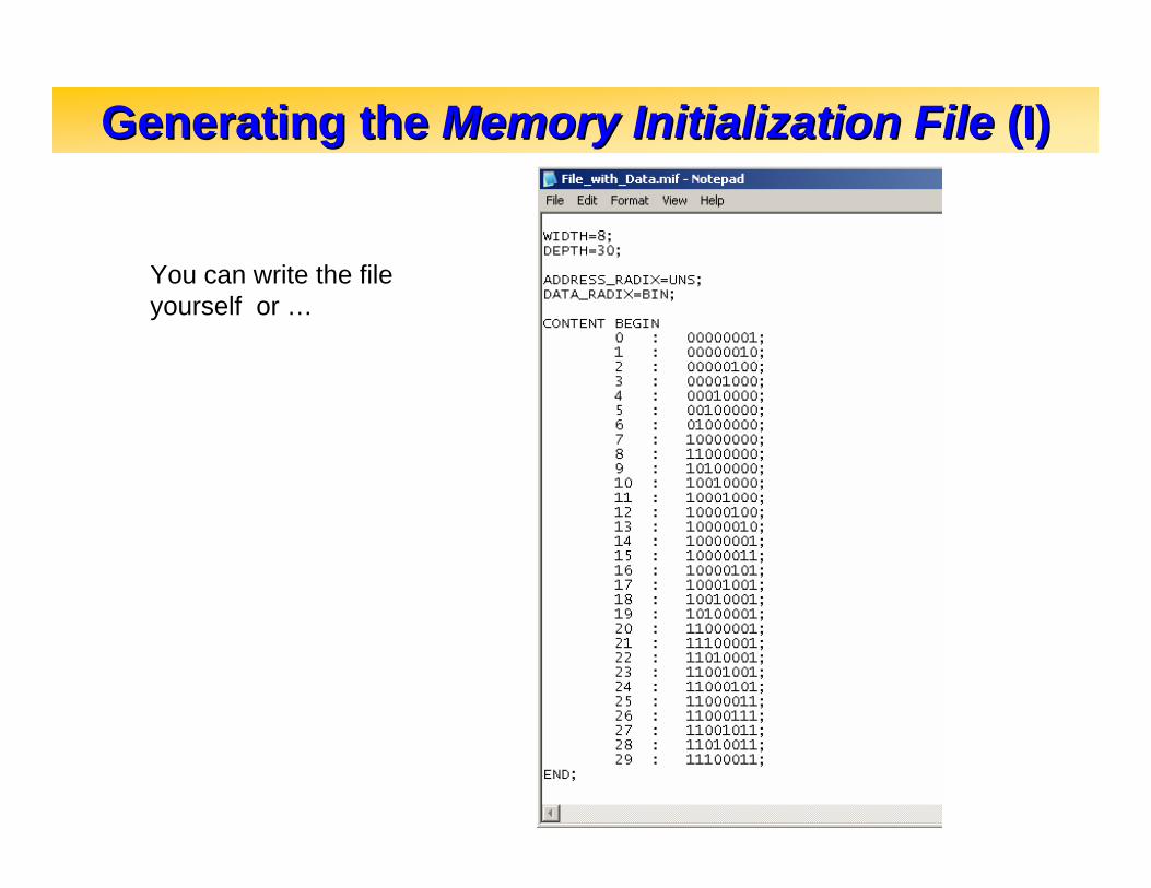
Generating the Generating the Memory Initialization File Memory Initialization File (I)(I)
You can write the file yourself or …

Generating the Generating the Memory Initialization File Memory Initialization File (II)(II)You can use Quartus II to generate the file using the Memory Editor:
Select: New File
Other Files
Memory Initialization File

Memory Initialization FileMemory Initialization File EditorEditor
88--bit wordbit word(enter by hand)(enter by hand)
word memory addressword memory address
RightRight--clickclick to enter type memory information: integer, hexadecimal, binary,to enter type memory information: integer, hexadecimal, binary, etc etc ……

Logic Element or RAM memory ?Logic Element or RAM memory ?If your memory space is not very large, the compiler will automatically choose to implement your Verilog circuit with D-type flip-flops of the Logic Elements.
You can force the compiler to use the dedicated FPGA memory:
Assignments > Settings >
Click hereClick here

Logic Element or RAM memory ?Logic Element or RAM memory ?If your memory space is not very large, the compiler will automatically choose to implement your Verilog circuit with D-type flip-flops of the Logic Elements.
You can force the compiler to use the dedicated FPGA memory:
Assignments > Settings >
turn ONturn ON

Dedicated Memory UsageDedicated Memory UsageCheck compiler report for memory usage:
Dedicated Memory UsageDedicated Memory Usage