organizing committee - nanyang technological universityalfred tok, nanyang technological university...
TRANSCRIPT


Organizing Committee
Associate Professor Xiaodong Chen (Chairman)
School of Material Science and Engineering, NTU
Professor Zhenan Bao (Co-Chair)
Department of Chemical Engineering, Stanford University
Professor Bo Liedberg
School of Materials Science and Engineering, NTU
Professor Peng Chen
School of Chemical and Biomedical Engineering, NTU
Assistant Professor Nripan Mathews
School of Materials Science and Engineering, NTU
Symposium Schedule
Nov 16, Monday
8:30 – 9:00 Registration
Session 1 Chair: Xiaodong Chen
9:00 – 9:15 Opening Remarks by Prof. Subbu Venkatraman, Chair of MSE
9:15 – 10:00 Skin-Inspired Flexible and Stretchable Electronic Sensors
Zhenan Bao, Stanford University
10:00 – 10:30 Stretchable Devices for Wearable Healthcare
Dae-Hyeong Kim, Seoul National University
10:30 – 10:50 Photo, Coffee Break and Poster Session
Session 2 Chair: Peng Chen
10:50 – 11:20 Printed and Flexible Sensors for Vital Signs Monitoring
Aminy Ostfeld, University of California, Berkeley
11:20 – 11:50 Ultrathin Gold Nanowires as New e-Skin Materials for Applications in
Flexible Transparent Conductor and Stretchable Wearable Sensors
Wenlong Cheng, Monash University
11:50 – 12:20 Horizontally Aligned CNT Biosensors for Sports Applications
Alfred Tok, Nanyang Technological University
12:20 – 12:50 Lunch
Session 3 Chair: Nripan Mathews
12:50 – 1:10 SPM Characterization of Flexible Materials for Biological Applications
Technical presentation by Bruker Nano Surfaces Division
1:10 – 1:30 Technical presentation by Leica Microsystems
1:30 – 2:00 Imperceptible Active Sensors for Cyber–physical Systems
Tsuyoshi Sekitani, Osaka University
2:00 – 2:30 High Dynamic Range Flexible All-Organic Photo Sensors with an Integrated
Architecture
Wenping Hu, The Chinese Academy of Sciences
2:30 – 3:00 When MEMS Technology Meets Flexible Electronics
Chengkuo Lee, National University of Singapore
3:00 – 3:30 CMOS Technology for Free Form Flexible-Stretchable-Reconfigurable
Electronics
Muhammad Mustafa Hussain, King Abdullah University of Science and
Technology

3:30 – 4:00 Coffee Break and Poster Session
Session 4 Chair: Zhenan Bao
4:00 – 4:30 Conductive Inks for 2D and 3D Printed Devices
Shlomo Magdassi, The Hebrew University of Jerusalem
4:30 – 5:00 Carbon Nanotube Based Electronic Devices
Qing Zhang, Nanyang Technological University
5:00 – 5:30 Construction of Flexible Organic Transistors and Thermoelectric Devices
towards Smart Elements
Chong-an Di, The Chinese Academy of Sciences
5:30 – 6:00 Towards Transparent Flexible Devices
Nripan Mathews, Nanyang Technological University
6:00 – 9:00 BBQ at President’s Lodge for all speaker and poster presenters
Nov 17, Tuesday
Session 5 Chair: Bo Liedberg
9:00 – 9:30 Hybrid Transparent Conductor for Deformable Display
Pooi See Lee, Nanyang Technological University
9:30 – 10:00 Stretchable and Flexible Transparent Conductive Electrodes
Hyoyoung Lee, Sungkyunkwan University
10:00 – 10:30 Coffee Break and Poster Session
10:30 – 11:00 Two Dimensional Material based Sensor for Wearable Electronics
Jong-Hyun Ahn, Yonsei University
11:00 – 11:30 Highly Flexible and Wearable Liquid-based Microfluidic Tactile Sensor
Chwee Teck Lim, National University of Singapore
11:30 – 11:40 Poster award ceremony and
Closing speech by Prof Russell Gruen, Director of NITHM
11:45 – Lunch at Fusion Spoon for all speakers

I1
Skin-Inspired Flexible and Stretchable Electronic Sensors
Zhenan Bao
Stanford University, Department of Chemical Engineering, Stanford, California 94305, USA
E-mail: [email protected]
Skin is the body’s largest organ, and is responsible for the transduction of a vast
amount of information. This conformable, stretchable and biodegradable material
simultaneously collects signals from external stimuli that translate into information, such as
pressure, pain and temperature. The development of electronic sensors, inspired by the
complexity of this organ, is a tremendous, unrealized materials challenge. However, the
advent of organic and carbon-based electronic materials may offer a potential solution to this
longstanding problem. In this talk, I will describe organic and carbon nano-electronic sensors
to mimic skin sensing functions. An artificial system that closely mimics the digital nature of
human skin mechanoreceptor for neuro-prosthetics using flexible printed organic electronic
circuits and pressure sensors will be presented.
Biography:
Zhenan Bao is a Professor of Chemical Engineering at Stanford
University, and by courtesy, a Professor of Chemistry and
Professor of Materials Science and Engineering. Prior to joining
Stanford University in 2004, she was a Distinguished Member of
Technical Staff at Bell Labs, Lucent Technologies from
1995-2004. She has over 350 refereed publications and over 50 US
patents with a Google Scholar H-Index of >110. Bao has served as
a Board Member for the National Academy Board on Chemical
Sciences and Technology and Board of Directors for the Materials
Research Society (MRS). She is an Associate Editor for Chemical
Sciences. She serves/served on the international advisory boards
for Nature Asia Materials, Journal of American Chemical Society, Advanced Materials,
Advanced Functional Materials, Advanced Energy Materials, Advanced Electronic Materials,
ACS Nano, Chemistry of Materials, Nanoscale, Chemical Communication, Macromolecules,
Organic Electronics, Materials Horizon and Materials Today.
She is also a Fellow of ACS, AAAS, MRS, SPIE, ACS PMSE and ACS POLY. Bao
was the recipient of the AICHE Andreas Acroivos Award for Professional Progress in
Chemical Engineering in 2014, ACS Polymer Division Carl S. Marvel Creative Polymer
Chemistry Award in 2013, ACS Author Cope Scholar Award in 2011, Royal Society of
Chemistry Beilby Medal and Prize in 2009, IUPAC Creativity in Applied Polymer Science
Prize in 2008, American Chemical Society Team Innovation Award in 2001 and the R&D
100 Award in 2001. Bao was selected by MIT Technology Review magazine in 2003 as one
of the top 100 young innovators. She is among the world’s top 100 materials scientists
acknowledged by Thomson Reuters. She is a co-founder and on the Board of Directors for C3
Nano, a Silicon Valley venture funded start-up commercializing flexible transparent
electrodes using nanomaterials.
I2
Stretchable Devices for Wearable Healthcare
Dae-Hyeong Kim1,2
1Center for Nanoparticle Research, Institute for Basic Science, 2School of Chemical and Biological Engineering,
Seoul National University, Seoul 151-744, Korea
Tel.:82-2-880-1565, E-mail: [email protected]
Recent advances in soft electronics have attracted great attention due in large to the
potential applications in personalized, bio-integrated healthcare devices. The mechanical
mismatch between conventional electronic/optoelectronic devices and soft human
tissues/organs causes many challenges, such as the low signal to noise ratio of biosensors due
to the incomplete integration of rigid devices with the body, inflammations and excessive
immune responses of implanted stiff devices originated from friction and foreign nature to
biotic systems, and the huge discomfort and consequent stress to users in wearing/implanting
these devices. Ultra-flexible and stretchable electronic/optoelectronic devices utilize low
system modulus and the intrinsic system-level softness to solve these issues. Here, we
describe our unique strategies in the synthesis of nanoscale materials, their seamless assembly
and integration, and corresponding device designs towards wearable and implantable
healthcare devices. Good examples include wearable quantum dot light emitting diodes
(QLEDs) potentially used for input/output routes for medical information used in integrated
healthcare sensors and transdermal therapeutic devices, as well as the multifunctional
implantable electronic stent and minimally invasive surgical tools to solve specific
cardiovascular and colorectal diseases respectively. These implantable and wearable
bio-electronic systems combine recent breakthroughs in unconventional soft electronics to
address unsolved issues in clinical medicine, hence providing new opportunities in
personalized healthcare.
Biography:
Dae-Hyeong Kim received his B.S. (2000) and M.S. (2002)
degrees from the School of Chemical Engineering at Seoul
National University. He obtained his Ph.D. (2009) from the
department of Materials Science and Engineering at the University
of Illinois at Urbana-Champaign. Since he joined the faculty of the
School of Chemical and Biological Engineering at Seoul National
University in 2011, he has focused on stretchable electronics for
bio-medical and energy applications.

I3
Printed and Flexible Sensors for Vital Signs Monitoring
Aminy Ostfeld and Ana Claudia Arias
Department of Electrical Engineering and Computer Sciences,
University of California, Berkeley, California 94720, USA
E-mail: [email protected]
In recent years, there has been an increased demand for wearable devices, capable of
monitoring stress and human performance during physically demanding tasks and fitness
levels. Wearable medical devices, for improved in-home care, customized for patients with
known health issues, who can benefit from regular and even continuous monitoring, are also
desired. Regular monitoring of vital signs would help to establish an individual’s health
statistics baseline and alert users and medical professionals of abnormalities, indicating that
further medical attention and care may be necessary. The minimal functionality desired for
wearable medical devices requires monitoring of vital signs, such as ECG, temperature, blood
oxygenation, pulse rate, blood pressure and respiration rate. We have developed methods to
measure pulse rate, blood oxygenation, bio-impedance and temperature using fully printed
devices as building blocks for flexible wearable sensing systems. Our sensors are fabricated
on flexible substrates using printed technologies, which allow integration of components,
hence maintaining the overall sensor flexibility. We have successfully implemented organic
light emitting diodes in an all-organic optoelectronic pulse oximeter sensor that functions in
transmission and reflection mode. Thermistors are inkjet-printed using a blend of
PEDOT:PSS and nickel oxide nanoparticles. Printed thermistors provide linear response from
25°C to 150°C with a controllable β of 500-1000. Bio-potential and ECG electrodes are
inkjet-printed using gold nanoparticle ink, where minimum feature size of 80 µm was
achieved with a sheet resistance of 0.4 Ω/sq. Finally, the sensors were interfaced with an
analog front-end, a microcontroller, and a Bluetooth chip, to provide ECG signal and accurate
body temperature. As part of the flexible system, we have developed flexible lithium ion
batteries based on graphite (anode) and lithium cobalt oxide (cathode). The battery operates
between 4.2-3.6 V and has a capacity of ~23 mAh (active area = 10.9 cm2) with capacity
retention of 99.2% after 100 electrochemical cycles. The battery was able to power a
commercial oximeter with 20 mA at a 3.6 V requirement.
Biography:
Ana Claudia Arias is an Associate Professor at the Electrical
Engineering and Computer Sciences Department at the University of
California, Berkeley, and a faculty director at the Berkeley Wireless
Research Center (BWRC) and the SWARM Lab. Prior to joining the
University of California, she was the Manager of the Printed
Electronic Devices Area and a Member of Research Staff at PARC, a
Xerox Company, in Palo Alto, California. She went to PARC from
Plastic Logic in Cambridge, UK, where she led the semiconductor
device group. She received her Ph.D. on semiconducting polymer
blends for photovoltaic devices from the Physics Department at the
University of Cambridge, UK. Prior to that, she received her master
and bachelor degrees in physics from the Federal University of Paraná

in Curitiba, Brazil. Her research focuses on devices based on solution processed materials and
applications development for flexible sensors and electronic systems. She is also the Chair of
the Thin Film Electronics Technical Advisory Council.

I4
Ultrathin Gold Nanowires as New e-Skin Materials for Applications in
Flexible Transparent Conductor and Stretchable Wearable Sensors
Wenlong Cheng1,2
1Department of Chemical Engineering, Monash University, Room 302, NH Building 82,
Melbourne, Victoria 3800, Australia 2Melbourne Centre for Nanofabrication, 151 Wellington Road, Melbourne, Victoria 3800,
Australia
E-mail: [email protected]
Group Page: http://users.monash.edu.au/~wenlongc
Future electronic devices will be soft and stretchable, enabling applications which
were previously impossible to achieve with existing rigid circuitry board technologies.
However, we need new materials and/or new design principles. In this talk, I will describe our
recent success in using ultrathin gold nanowires as a new class of electronic skin (e-skin)
material. We demonstrated their applications as flexible transparent conductor1 and in highly
stretchable wearable sensors2-4. In particular, we could obtain highly stretchable nano-patches
or tattoos, which are body attachable, and could be integrated into textile, enabling monitoring
of wrist pulses, hand gestures, body motions and controlling robotic arms in a wireless
fashion. I will also briefly cover our recent work in the fabrication of flexible/stretchable
sensors with bio-inspired design5 and copper nanowires6-7.
Biography:
Wenlong Cheng is a full professor in the Department of Chemical
Engineering at Monash University, Australia. He earned his Ph.D.
from the Chinese Academy of Sciences in 2005 and his B.S. from Jilin
University, China in 1999. He held positions in the Max Planck
Institute of Microstructure Physics and the Department of Biological
and Environmental Engineering in Cornell University before joining
Monash University in 2010. His research interest lies at the nano-bio
interface, particularly addressing plasmonic nanomaterials, DNA
nanotechnology, nanoparticle anticancer theranostics and electronic
skin. He has published ~70 papers, including 3 in Nature
Nanotechnology, 1 in Nature Materials and 1 in Nature
Communications.
1. Y. Chen, Z. Ouyang, M. Gu and W. L. Cheng*, “Mechanically Strong, Optically
Transparent, Giant Metal Superlattice Nanomembranes From Ultrathin Gold Nanowires,”
Advanced Materials, 2013, 25, 80-85.
2. S. Gong, W. Schwalb, Y. Wang, Y. Chen, Y. Tang, J. Si, B. Shirinzadeh and W. L.
Cheng*, “A wearable and highly sensitive pressure sensor with ultrathin gold nanowires,”
Nature Communications, 2014, 5, 3132.
3. S. Gong, D. T. H. Lai, B. Su, K. J. Si, Z. Ma, L. W. Yap, P. Guo and W. L. Cheng*,
“Highly Stretchy Black Gold E-Skin Nanopatches as Highly Sensitive Wearable

Biomedical Sensors,” Advanced Electronic Materials, 2015, DOI:
10.1002/aelm.201400063.
4. S. Gong, D. Lai, Y. Wang, L. W. Yap, K. J. Si, Q. Shi, N. N. Jason, T. Sridhar, H. Uddin
and W. L. Cheng*, “ Tattoo-like Polyaniline Microparticle-Doped Gold Nanowire Patches
as Highly Durable Wearable Sensors,” ACS Applied Materials and Interfaces, Accepted,
DOI:10.1021/acsami.5b05001.
5. B. Su*, S. Gong, Z. Ma, L. W. Yap and W. L. Cheng*, “Mimosa-inspired design of
flexible pressure sensor with touch sensitivity,” Small, 2014, DOI:
10.1002/small.201403036.
6. N. N. Jason, W. Shen and W. L. Cheng*, “Copper Nanowires as Conductive Ink for
Low-Cost Draw-On Electronics,” ACS Applied Materials and Interfaces, 2015, 7,
16760–16766.
7. Y. Tang, S. Gong, Y. Chen, L. W. Yap and W. L. Cheng*, “Manufacturable Conducting
Rubber Ambers and Stretchable Conductors from Copper Nanowire Aerogel
Monoliths,” ACS Nano, 2014, 8, 5707-5714.

I5
Horizontally Aligned CNT Biosensors for Sports Applications
Hu Chen1,2,4, Jingfeng Huang1,2, Alagappan Palaniappan1,3, Bo Liedberg1,3, Mark Platt4,
Alfred Iing Yoong Tok1,2,*
1School of Materials Science and Engineering,
Nanyang Technological University, 50 Nanyang Avenue, Singapore 639798 2Institute for Sports Research,
Nanyang Technological University, 50 Nanyang Avenue, Singapore 639798 3Centre for Biomimetic Sensor Science,
Nanyang Technological University, 50 Nanyang Drive, Singapore 637553 4Department of Chemistry, Centre for Analytical Science, Loughborough University,
Loughborough, Leicestershire LE11 3TU, UK
*Presenting author
An ultra-sensitive and miniaturized biosensor is widely needed for real time
monitoring in the field of sports science. In this work, we present a novel biosensor based on
horizontally aligned carbon nanotubes (CNTs) with great potential for various applications in
sports science. The CNTs were synthesized on quartz substrates, followed by device
fabrication. As a demonstration of their biosensing capability, the developed devices were
used for the detection of interleukin-6 (IL-6), a key biomarker for the prevention of sports
science issues, such as over-training. The experimental results revealed that the as-prepared
sensors responded to the biomarkers immediately in the range of 10-100 ng/mL and the
limit-of-detection (LOD) was 1 pg/mL. By virtue of the rapid sensor response, excellent
sensitivity and good portability, the CNT-based biosensor presented is an ideal candidate for
real time monitoring of athletes in training sessions as the sensing molecules can easily be
developed to sense a host of other sport-related biomarkers.
Biography:
Alfred Tok (PK; Ph.D., NTU; C.Eng, MIMMM; MBA, NTU)
has been a faculty member in the School of Materials Science
and Engineering (MSE) since 2003. He studied Mechanical
Engineering at the Queensland University of Technology,
Australia, and graduated with First Class honours in 1995. He
was also conferred the Dean's Award for Excellence for being
the top graduate on the course. After graduation, he worked as a
mechanical engineer at ST Aerospace Engineering. In 1997, he
was awarded 2 scholarships at Nanyang Technological
University to pursue his Ph.D. in Mechanical Engineering. He obtained his MBA (Dean’s
List) in 2009 from the Nanyang Business School, and in 2009, he was appointed Division
Head of Materials Technology in MSE (till 2012). Since 2011, he has been the Deputy
Director of the Institute for Sports Research in NTU. He also consults extensively for
companies from various industries.

I6
Imperceptible Active Sensors for Cyber-Physical Systems
Tsuyoshi Sekitani, Teppei Araki, Shusuke Yoshimoto, Takafumi Uemura
The Institute of Scientific and Industrial Research, Osaka University
8-1, Mihogaoka, Ibaraki, Osaka 567-0047, Japan
E-mail: [email protected]
In this talk, I will discuss the recent progresses and future prospects of large-area,
ultra-flexible and ultrathin electronic sensors. Our work focuses on integration technologies
of thin-film electronics comprising ultra-soft gel electrodes, thin-film amplifier, Si-LSI
platform, thin-film battery, and information engineering, which are all integral for the
realization of imperceptible active sensors. Here, I would like to demonstrate the applications
of imperceptible sensors for patch-type bio-signal monitoring sheets. These sensors serve as
an important part of seamless cyberspace/real-world interfaces that are commonly referred to
as cyberphysical systems (CPSs).
On the basis of our initial work on manufacturing different flexible organic devices,
including TFTs, LEDs, and PDs, we developed ultra-flexible electronics for applications that
use large-area sensors, actuators, memories, and displays1-13. For example, by taking
advantage of an ultra-flexible and compliant amplifier that can amplify biological signals by
500×, we developed 1 µm thick multi-channel active matrix electrocardiogram and
electromyogram monitoring systems. Ultrathin electronics with a total thickness of
approximately 1-2 µm support a bending radius of less than 10 µm.
Biography:
Tsuyoshi Sekitani received his Ph.D. in applied physics from the
University of Tokyo, Japan in 2003. From 1999-2003, he was
with the Institute for Solid State Physics at the University of
Tokyo. From 2003- 2010, he was a Research Associate, and in
2011, he was an Associate Professor in the School of
Engineering at the University of Tokyo. In 2014, he was made a
professor in The Institute of Scientific and Industrial Research at
Osaka University. His current research interests include organic
transistors, flexible electronics, plastic integrated circuits,
large-area sensors, and plastic actuators. He is a member of the
Japanese Society of Applied Physics (JSAP) and the Materials
Research Society (MRS). He has received more than 27 awards, including the Young
Scientist Award from the Minister of Education, Culture, Sports, Science and Technology,
Japan, and the IEEE Paul Rappaport Award in 2009 and 2010 (Best Paper at the IEEE
Transactions on Electron Devices in 2009 and 2010). In 2014, he was acknowledged as one of
the “Highly Cited Researchers” (The World’s Most Influential Scientific Mind) by Thomson
Reuters.
1. T. Sekitani, et al., Nature Materials, 6, 413 (2007).
2. T. Sekitani, et al., PNAS, 105, 4976 (2008).
3. T. Sekitani et al., Science, 321, 1468 (2008).

4. T. Sekitani, et al., Nature Materials, 8, 494 (2009).
5. T. Sekitani, et al., Science, 326, 1516 (2009).
6. T. Sekitani, et al., Nature Materials, 9, 1015 (2010).
7. K. Kuribara, et al., Nature Communications, 3, 723 (2012).
8. M. Kaltenbrunner, et al., Nature Communications, 3, 770 (2012).
9. T. Yokota, et al., IEEE Transactions on Electron Devices, 59, 3434 (2013).
10. M. Kaltenbrunner, et al., Nature, 499, 458 (2013).
11. M. S. White, et. al., Nature Photonics, 7, 811 (2013).
12. S. Lee, et. al., Nature Communications, 5, 5898 (2014).
13. M. Melzer, et. al., Nature Communications, 6, 6080 (2015).

I7
High Dynamic Range Flexible All-Organic Photo Sensors with an
Integrated Architecture
Hanlin Wang1,2, Hongtao Liu1, Qiang Zhao1,2, Cheng Cheng1, Wenping Hu1, Yunqi Liu1
1Beijing National Laboratory for Molecular Sciences, Key Laboratory of Organic Solids,
Institute of Chemistry, Chinese Academy of Sciences, Beijing 100190, China 2University of Chinese Academy of Sciences, Beijing 100049, China
E-mail: [email protected]
Organic materials can complement conventional inorganic materials for
cost-effective optoelectronics, such as photo sensors. However, due to difficulties in
integration of organic components, the exploration of all-organic photo sensors remains a
challenge. Here, we demonstrate multi-component integrated, all-organic photo sensors with
an overall dynamic range of nearly 108. Based on photoconductivity differences in organic
dyes, a photosensitive voltage divider is realized by a series connection of organic resistors.
By virtue of an organic field-effect transistor as an amplifier, grey scale sensing is achieved in
our pixels. The devices are ultrathin (470 nm) and extremely light, (850 mg m−2), however,
they continue to be operational when folded with a bending radius of 5 µm. The innovative
combination of organic components, together with the simplicity of our processing technique,
might provide opportunities for smart plastic optoelectronics, such as remote control devices
and emerging health monitoring systems.
Biography:
Wenping Hu is a Professor at the Institute of Chemistry, Chinese
Academy of Sciences. He received his Ph.D. from the same
institute in 1999. Subsequently, he joined Osaka University and
Stuttgart University as a Research Fellow, funded by the Japan
Society for the Promotion of Sciences and Alexander von
Humboldt Fellowship, respectively. In 2003, he worked in
Nippon Telephone and Telegraph (NTT), and then joined the
Institute of Chemistry, Chinese Academy of Sciences, and was
promoted to full professor. He served as a Visiting Scholar at the
Department of Chemistry, Stanford University in 2007 and was a
Visiting Professor at the Department of Chemistry, National
University of Singapore in 2013. He focuses on organic
optoelectronics and has published 4 books (Organic Optoelectronics, Wiley, etc.) and more
than 350 peer-reviewed papers with total citations >10,000. He is a member of the editorial
boards for several journals (e.g., Advanced Energy Materials, Advanced Electronic Materials,
Nano Research, Science China Chemistry, Science Bulletin, Science China Materials), and is
now an Associate Editor of Polymer Chemistry.

I8
When MEMS Technology Meets Flexible Electronics
Chengkuo Lee
Singapore Institute for Neurotechnology (SINAPSE)
Centre for Sensors and MEMS
Department of Electrical and Computer Engineering
National University of Singapore
The advance in MEMS technology has brought significant impact on human life.
Inertial sensors have dominated many innovative and profitable commercial applications in
the past few years. Ranging from wearable electronics to inter-of-things (IoT), more and more
MEMS sensors have become the enabling technology for novel applications. The combination
of flexible electronics, flexible and stretchable sensors, MEMS sensors, microfluidics and
energy harvesters will form a new platform for healthcare applications. In this talk, such
platforms will be highlighted, while transdermal drug delivery and neural interfaces are
introduced as demonstrators.
Biography:
Chengkuo Lee received his Ph.D. in Precision Engineering in February
1996 from the University of Tokyo. He worked as a JST Research
Fellow in the Mechanical Engineering Laboratory, AIST, MITI, Japan
in 1996. He was an Adjunct Assistant Professor in the Electrophysics
Department at the National Chiao Tung University, Hsinchu, Taiwan, in
1998, and an Adjunct Assistant Professor at the Institute of Precision
Engineering at National Chung Hsing University, Taichung, Taiwan,
from 2001-2005. In August 2001, he co-founded Asia Pacific
Microsystems, Inc. (APM), in Hsinchu, Taiwan, where he became Vice President of R&D
before becoming Vice President of the optical communication business unit. He was also in
charge of international business and technical marketing for the MEMS foundry service. From
2006-2009, he was a Senior Member of the Technical Staff at the Institute of Microelectronics,
A*STAR, Singapore. Currently, he is an Associate Professor in the Department of Electrical
and Computer Engineering, and the Director of Centre for Intelligent Sensors and MEMS at
National University of Singapore. He is the co-author of Advanced MEMS Packaging
(McGraw-Hill, 2010) and Micro- and Nano-Energy Harvesting Technologies (Artech House,
2015). He has contributed to more than 250 international conference papers and extended
abstracts, and 185 peer-reviewed international journal articles in the fields of sensors,
actuators, energy harvesting, MEMS, lab-on-chip, NEMS, nanophotonics and
nanotechnology.

I9
CMOS Technology for Free Form Flexible-Stretchable-Reconfigurable
Electronics
Muhammad Mustafa Hussain
Integrated Nanotechnology Lab, Electrical Engineering, Computer Electrical Mathematical
Science and Engineering Division, King Abdullah University of Science and Technology
(KAUST), Thuwal 23955-6900, Saudi Arabia
E-mail: [email protected]
Complementary metal oxide semiconductor (CMOS) technology has served as a
critical catalyst to the rise and prominence of our digital world. Singular focus on
performance per cost has driven CMOS technology to be increasingly mature and reliable in
batch fabrication of high quality electronics, based on predominantly mono-crystalline thin
film materials, like silicon, gallium nitride, III-V materials, etc. However, they are often rigid,
brittle and opaque. This restricts their usage in emerging free form
flexible-stretchable-reconfigurable electronics. In my talk, I will discuss how CMOS
technology can be used to transform such physically unbendable but state-of-the-art
electronics into flexible-stretchable-reconfigurable electronics, while retaining their high
performance, energy efficiency, ultra-large-scale-integration (ULSI) density and performance
per cost benefit. I will discuss integration strategies to rationally design materials, processes
and devices to facilitate this transformation. To do so, I will use examples focusing on
healthcare and environmental monitoring, which are commercially relevant or under
commercialization. Specially looking forward, we need to specify the attributes of electronics,
which will enable Internet of Everything, where nearly every object will be smart,
informative, interactive and resourceful to augment the quality of our life. In the past few
years, my group has particularly focused on defining such attributes, where we see live
(interactive), physically free form and democratized (easy and simple to use, make and afford)
electronics, which can realize wide deployment of electronics for smart living and sustainable
future.
Biography:
Before joining KAUST, Muhammad Mustafa Hussain (Ph.D., ECE, UT
Austin, December 2005) was Program Manager of the Emerging
Technology Program in SEMATECH, Austin. His program was funded
by DARPA NEMS, CERA and STEEP programs. A regular panelist of
US NSF grants reviewing committees, he is the Editor-in-Chief of
Applied Nanoscience (Springer) and an IEEE Senior Member. He has
served as first or corresponding author in 75% of his 214 research
papers (including 15 cover articles and 87 journal papers). He has 15
issued and pending US patents. His students are now serving as faculty
members and researchers in KFUPM, UC Berkeley, TSMC, KACST
and DOW Chemicals. Scientific American has listed his research as one of the Top 10 World
Changing Ideas of 2014. He has received 19 research awards including this year’s

Outstanding Young Texas Exes Award 2015 (UT Austin Alumni Award) and US National
Academies’ Arab-American Frontiers of Engineering, Science and Medicine 2015.
I10
Conductive Inks for 2D and 3D Printed Devices
Shlomo Magdassi
The Hebrew University of Jerusalem, Jerusalem 91904, Israel
E-mail: [email protected]
Nanomaterials have unique properties which enable their utilization in functional
printing. Our research is focused on synthesis and formulations of nanoparticles and inks, and
their utilization in printed devices. The formation and application of conductive inks
composed of silver, copper, copper@silver will be reported. These inks address a major
challenge in fabrication of flexible electronic devices, in which the printing should be
performed desirably at sufficiently low temperatures, which will not damage the polymeric
substrates. Our recent discoveries of achieving high conductivity by sintering even at room
temperature will be discussed. The fabrication of optoelectronic devices, such as smartphone
touchscreens and smart windows, will be presented, based on combining low sintering
temperature concepts with directed wetting and self-assembly processes. Application of 3D
printing technologies for fabrication of electrodes, comprising responsive shape memory
objects, will be also demonstrated.
Biography:
Shlomo Magdassi is a Professor of Chemistry at the Casali Center
of Applied Chemistry, the Institute of Chemistry and the Center for
Nanoscience and Nanotechnology at the Hebrew University of
Jerusalem, Israel. His research focuses on formation, formulation
and applications of micro- and nanoparticles. These particles can be
used as active components in functional inks and coatings, for
example, conductive inks for electronic devices, and 2D and 3D
functional printing. In addition to his scientific publications, he has
various inventions on applications of colloids in industrial products,
which led to some industrial activities, such as worldwide sales and
establishing new companies. For more information, please see:
http://chem.ch.huji.ac.il/casali/magdassi/magdassi.htm

I11
Carbon Nanotube Based Electronic Devices
Qing Zhang
Centre for Micro-/Nano-electronics (NOVITAS), School of Electrical and Electronic
Engineering, Nanyang Technological University, Singapore
Tel: (+65) 6790-5061, E-mail: [email protected]
In this talk, I shall review our recent research activities on carbon nanotubes (CNTs)
based electronic devices. The talk can be divided into four parts, i.e., functionalized CNTs for
sensing applications, CNTs-based soft electronics, CNTs-based OLED drivers and
CNTs-based soft Li-ion batteries.
We found that a semiconducting-to-metallic CNT transition can be realized upon
dichlorocarbene functionalization. The transition is reversible upon thermal annealing under
ambient conditions. The electrical properties of m-CNTs remain largely unaffected whereas the
on-state conductivity of s-CNTs is greatly reduced by this process. This is in agreement with
relevant theoretical predictions. We also found that after covalently functionalized with 10 µM
4-BBDT solution, the CNT network can be used as a promising humidity sensing element.
We employed a novel post transfer technique to prepare CNT-based soft electronic
devices. All CNT devices are initially fabricated on a hard substrate and subsequently
encapsulated onto polyimide (PI) and peeled off from the hard substrate to form flexible
devices. The soft transfer medium used here serves as the flexible substrate after a plastic
transformation process so that the devices and circuits are encapsulated onto the flexible plastic,
in favour of high flexibility and reliability.
We also demonstrated the first CNT-based thin film transistor (TFT) driver circuits for
static and dynamic AM OLED display with 6 × 6 pixels. High device yields and performance
uniformity are achieved using randomly-grown SWNT networks as the active channel material
for the TFTs. High device mobility of ~45 cm2V-1s-1 and the high channel current on/off ratio of
~105 of the CNT-TFTs fully guarantee the control capability to the OLED pixels.
We confirmed a layer-by-layer assembly technique as a facile and scalable method to
prepare a multilayer Si/CNT coaxial nanofiber anode which possesses storage capacity above 1
mAh cm-2. The prepared Si/CNT coaxial nanofiber anodes show excellent cyclability. The
excellent performance of the Si/CNT coaxial nanofiber multilayer anodes is attributed to the
unique nanostructure. The CNT network matrix offers mechanical support to accommodate the
stress associated with the large volume change of Si coating and the nanoporous multilayer
structure provides continuous paths for Li ion and electron transport. In addition, we developed
high capacity 3D current collectors for flexible battery electrodes. We grew vertically aligned
CNT arrays directly on carbon cloth (CC) as a hierarchical 3D current collector and load
amorphous Si onto the CNT array with a large areal mass density. Benefiting from the porous
structure and hierarchical 3D conductive pathway, the as-synthesized hierarchical 3D CNT-Si

arrays on CC electrode exhibits a high areal capacity up to 3.32 mAh cm-2 at a current density of
0.2 mA cm-2, which is superior cycle performance with a capacity retention of 94.4% after 200
cycles at a high current density of 1 mA cm-2, and excellent rate capability.
Biography:
Qing Zhang is a Professor and the Director of Centre of
Micro-/Nano-electronics at the School of Electrical and Electronic
Engineering, Nanyang Technological University, Singapore. His
research interests cover nanomaterials and nano/micro-electronic
devices, carbon/silicon based thin films, etc. His attention is focused on
carbon nanotube and other 0-D, 1-D and 2-D nanostructure based
devices and fundamentals, etc.
I12
Construction of Flexible Organic Transistors and Thermoelectric Devices
towards Smart Elements
Chong-an Di and Daoben Zhu
Key Laboratory of Organic Solids,
Institute of Chemistry, Chinese Academy of Sciences, Beijing, 100190, China
E-mail: [email protected]
Organic devices are promising candidates for next-generation flexible smart
products, owing to their intrinsic light weight, prominent flexibility, and potential for low-cost
development.1,2 Benefiting from systematic studies on functional materials and device
engineering,3,4 we report a series of flexible sensing devices, such as pressure sensors,
chemical-/bio-sensors, magnetic sensors utilizing organic thin-film transistors (OTFTs) and
organic thermoelectric devices (OTEs).5-8 As an example, we propose the construction of
flexible suspended gate OTFTs (SGOTFTs) using a simple lamination method.5 By
combining OTFTs with a suspended gate device geometry, the SGOTFTs provide an effective
way for ultra-sensitive pressure detection. The fabricated devices displayed an unprecedented
sensitivity of 192 kPa-1 and a low limit-of-detection pressure of 0.5 Pa, which was achieved
by fine-tuning the material properties of the suspended gate, allowing their applications in
health monitoring and spatial pressure mapping.7 More recently, we demonstrated
temperature-pressure dual-parameter sensors, utilizing microstructure-frame-supported
organic thermoelectric (MFSOTE) materials by utilizing combined thermoelectric and
piezo-resistive effects in a single device.8 The effective transduction of temperature and
pressure stimuli into two independent electrical signals permits the instantaneous sensing of
temperature and pressure with an accurate temperature resolution of 0.1 K and a high pressure
sensing sensitivity of up to 28.7 kPa-1. The excellent sensing performance, prominent
flexibility and self-powered features of the MFSOTE devices make them promising
candidates in several artificial intelligence and health-care systems.
Biography:
Chong-an Di received his Ph.D. in chemistry from the Institute of
Chemistry, Chinese Academy of Sciences (ICCAS) in 2008. He was
appointed Assistant Professor in 2008 and promoted to Associate
Professor in 2010 at ICCAS. He visited University of Cambridge and
Stanford University as a visiting and senior visiting academic in 2011
and 2013, respectively. Currently, his research focuses on the
investigation of organic field-effect transistors and organic
thermoelectric devices. Since 2005, he has authored or co-authored
more than 100 peer-reviewed articles in Accounts of Chemical
Research, Nature Communications, Journal of the American
Chemical Society, Advanced Materials, etc., and is named in 12
patents.
1. C. A. Di, F. J. Zhang, D. B. Zhu, Advanced Materials, 2013, 25, 313.

2. Y. P. Zang, F. J. Zhang, C. A. Di, D. B. Zhu, Materials Horizon, 2015, 2, 140.
3. Y. Zhao, C. A. Di, X. K. Gao, Y. B. Hu, Y. L. Guo, L. Zhang, Y. Q. Liu, J. Z. Wang,
W. P. Hu, D. B. Zhu, Advanced Materials, 2011, 23, 2448.
4. F. J. Zhang, Y. B. Hu, T. Schuettfort, C. A. Di, X. K. Gao, C. R. McNeil, L. Thomsen,
S. C. B. Mansfeld, W, Yun, H. Sirringhaus, D. B. Zhu, Journal of the American
Chemical Society, 2013, 135, 2338.
5. F. J. Zhang, C. A. Di, N. Berdunov, Y. Y. Hu, Y. B. Hu, X. K. Gao, Q. Meng, H.
Sirringhaus, D. B. Zhu, Advanced Materials, 2013, 25, 1401.
6. Y. P. Zang, F. J. Zhang, D. Z. Huang, C. A. Di, Q. Meng, X. K. Gao, D. B. Zhu,
Advanced Materials, 2014, 26, 2862.
7. Y. P. Zang, F. J. Zhang, D. Z. Huang, X. K. Gao, C. A. Di, D. B. Zhu, Nature
Communications, 2015, 6, 6269.
8. F. J. Zhang, Y. P. Zang, D. Z. Huang, C. A. Di, D. B. Zhu, Nature Communications,
2015, Accepted.

I13
Towards Transparent Flexible Devices
Nripan Mathews
School of Materials Science and Engineering
Nanyang Technological University, 50 Nanyang Avenue, Singapore 639798
Transparent semiconductors and devices allow for the development of novel
applications that can be integrated facilely onto a wide variety of surfaces. The development
of new material sets have to be combined with techniques for reducing the processing
temperatures and unlocking functionalities, such as printability. This talk will focus on the
development of amorphous metal oxide semiconductors for thin film transistor applications.
The effect of post processing protocols and cationic substitution in the realization of an
all-transparent transistor will be elucidated.
Biography:
Nripan Mathews is an Assistant Professor at Nanyang Technological
University, Singapore, where he holds a joint position at the School of
Materials Science and Engineering and Energy Research Institute @
NTU. His research focuses on solution-processed electronic materials
for applications in electronics and solar energy conversion. He is a
recipient of the TR35@Singapore Award 2014 and the
A*STAR-SNAS Young Scientist Award. His work has led to ~100
SCI journals publications with an H-Index of 30.

I14
Hybrid Transparent Conductor for Deformable Display
Pooi See Lee
School of Materials Science and Engineering
Nanyang Technological University, 50 Nanyang Avenue, Singapore 639798
E-mail: [email protected]
There is an impending need for transparent, yet conducting substrates to realize next
generation consumer devices with flexible and deformable functionalities. There are fueling
demands for alternative flexible displays, including electrochromics and electroluminescent
devices, which require transparent conducting electrodes. The conducting electrodes in
displays ideally possess superior conductivity and optical transparency under extreme
conditions, such as folding, stretching, flexing, rolling or crumpling. In this talk, I will
illustrate our approach in fabricating solution-processed hybrid transparent conductors, and
their applications in electrochromics and electroluminescent devices.
We have developed a transfer method to prepare hybrid transparent conductors with
high figure of merit. This effective transfer method improves the interface properties and
bonding stability between the conductive constituents and the matrix. Superior mechanical
properties and excellent electrical conductivity can be achieved. The transparent conductor
possesses active surfaces that improve the interfacial properties with the overlay active
materials with enhanced electron conduction, charge distribution, and ionic diffusion. We
demonstrate the foldable transparent conductors for flexible wearable electrochromics
devices. In addition, we show that stretchable electrochromics and electroluminescent devices
can also be fabricated using metallic nanowires with polydimethylsiloxane matrix, indicating
the promising potential of metallic nanowires based transparent conductors for deformable
display applications.
Biography:
Pooi See Lee is a Professor in the School of Materials Science and
Engineering, Nanyang Technological University, Singapore. She
obtained her B.Sc. (Honours) and Ph.D. from the National University of
Singapore. Her research work focuses on the theme of electrochemical-
and electrical-inspired devices based on nanostructures and
nanocomposites for applications in electrochromics, energy storages,
actuators, ferroelectrics, electrical memory devices, sensors, flexible
and stretchable electronics.

I15
Stretchable and Flexible Transparent Conductive Electrodes
Hyoyoung Lee1,2
1Center for Integrated Nanostructure Physics, Institute for Basic Science (IBS),
Sungkyunkwan University, Suwon 440-746, Korea 2Department of Chemistry, Department of Energy Science, SKKU Advanced Institute of
Nano Technology (SAINT), Sungkyunkwan University, Suwon 440-746, Korea
Recently, silver nanowires (AgNWs) have attracted considerable interest for their
potential applications in stretchable and flexible transparent conductive films (TCFs).
However, one challenge for commercialization of AgNW-based TCF is low conductivity and
low stability caused by weak adhesion forces between AgNWs and the substrate. Thus, the
adhesion force especially for attachment of AgNWs to the various kinds of substrates,
including plastic substrate for flexible and stretchable electrodes, becomes the most important
issue.
Here, we report stretchable and flexible transparent conductive AgNW films, which
were prepared by using two-dimensional (2-D) hydrophilic graphene oxide nanosheet (GO) as
an over-coating layer (OCL) on the hydrophilically surface-treated plastic film1. In addition,
poly(diallyldimethyl-ammonium chloride) (PDDA) was introduced as an adhesive agent onto
AgNW2. Further, the use of GO and PDDA for OCL was introduced via layer-by-layer (LbL)
assembly technique. We demonstrated that PDDA could increase the adhesion between
AgNW and substrate to form a uniform AgNW network, and could also serve to improve the
stability of GO OCL3. Our AgNW-PDDA-GO composite TCF is stable after exposure to H2S
gas or sonication3. Furthermore, for the stretchable TCF, polydimethylsilaoxane (PDMS)
surface with various silane compounds, which have functional groups with different degree of
sigma (σ)-donating ability and polarity, was modified. We observed different interfacial states
depending on terminated functional heap groups of molecularly self-assembled substrate. The
surface surrounded by [3-(2-aminoethylamino)propyl]trimethoxysilane exhibited the strongest
contact force on the substrate, especially on the junction side, and the longest maintenance of
hydrophilicity by coordination-type bonding. As a result, AgNWs adhered permanently to
stretchable substrates while simultaneously maintaining high transparency and high
conductivity, which suggests excellent mechanical durability, hence exhibiting enhanced
performance of flexibility and stretchability4. Finally, we report a novel method to prepare
new hybrid rGO-AgNP conducting film by carefully designed reduction duality of formic
acid at low temperature, which can be stretched5.
Biography:
Hyoyoung Lee received his B.S. and M.S. degrees in chemistry at Kyung
Hee University, Korea in 1989 and 1991, respectively. He received his
Ph.D. at the Department of Chemistry, University of Mississippi, USA, in
1997. He was subsequently a Postdoctoral Associate at North Carolina
State University, USA, from 1997-1999 and POSTECH, Korea, from
1999-2000. He worked at the Electronics and Telecommunications
Research Institute (ETRI) from 2000-2009 as team leader. He then moved
to Sungkyunkwan University and has served as a full professor at the
Department of Chemistry, lecturing Organic Chemistry. He served as a director of National

Creative Research Initiatives (NCRI), Center of Smart Molecular Memory from 2006-2015 and
has also served as an Associate Director of Institute of Basic Science (IBS) at SKKU. His
current research areas are on organic semiconducting materials and devices including
molecular/organic memory, OLED, OTFT, sensors, energy storage, graphene oxide, reduced
graphene oxide, 2D TMD and MXenes. He has written more than 100 journal articles. He is
also a member of the Korean Chemical Society (KCS), Materials Research Society (MRS) and
American Chemical Society (ACS).
1. In Kyu Moon et al., “2D Graphene Oxide Nanosheets as an Adhesive Over-Coating
Layer for Flexible Transparent Conductive Electrodes”, Scientific Reports, 3, 1112;
DOI: 10.1038/srep01112, 2013.
2. Y. Li et al., "Highly Bendable, Conductive and Transparent Film by an Enhanced
Adhesion of Silver Nanowires", ACS Applied Materials and Interfaces, 5(18),
9155-60, 2013.
3. H. Lee et al., "High Mechanical and Tribological Stability of an Elastic Ultrathin
Overcoating Layer for Flexible Silver Nanowire Films”, Advanced Materials, 13,
2252-9, 2015.
4. H. Lee et al., “Well-ordered and High Density Coordination-type Bonding to
Strengthen Contact of Silver Nanowires on Highly Stretchable Polydimethylsiloxane”,
Advanced Functional Materials, 24 (21), 3276-3283, 2014.
5. Yeoheung Yoon, et al., “Highly Stretchable and Conductive Silver Nanoparticle
Embedded Graphene Flake Electrode Prepared by In-situ Dual Reduction Reaction”,
Scientific Reports, 2015.

I16
Two-Dimensional Material Based Sensor for Wearable Electronics
Jong-Hyun Ahn
School of Electrical & Electronic Engineering, Yonsei University, Seoul 120-749, Korea
Two-dimensional (2-D) materials, including graphene and transition metal
dichalcogenides, provide outstanding properties that can be integrated into various flexible
and wearable electronic devices in a conventional, scalable fashion. The mechanical,
electrical and optical properties of 2-D materials make it attractive for applications in
wearable electronics, biosensors, and other systems. Here, we report flexible (or stretchable)
tactile sensors composed of large area 2-D materials grown by chemical vapor deposition
method. 2-D material based sensors were integrated on ultrathin plastic substrates and even
human skin. This ultrathin 2-D material based sensor has shown good characteristics in terms
of sensitivity, linearity, hysteresis and repeatability even on a human fingertip.
Biography:
Jong-Hyun Ahn received his Ph.D. from the
Department of Materials Science and Engineering,
POSTECH, Korea. He has published more than 120
papers in SCI-listed journals, including articles
published on Science (2), Nature (1), Nature Materials
(1), Nature Photonics (1), Nature Nanotechnology (3)
and Nano Letters (8). His total citation number is over
14,700.

I17
Highly Flexible and Wearable Liquid-based Microfluidic Tactile Sensor
Kenry1,2,3,#, Joo Chuan Yeo1,3,#, Chwee Teck Lim2,3,4,*
1NUS Graduate School for Integrative Sciences and Engineering,
National University of Singapore, Singapore 117456 2Centre for Advanced 2D Materials and Graphene Research Centre,
National University of Singapore, Singapore 117546 3Department of Biomedical Engineering, National University of Singapore, Singapore 117575
4Mechanobiology Institute, National University of Singapore, Singapore 117411
*Email: [email protected]
# both authors contributed equally to this work
We developed a novel liquid-based resistive microfluidic tactile sensor that possesses
high flexibility, durability and sensitivity. The tactile sensor comprises a soft elastomer-based
microfluidic template encapsulating a conductive liquid, which serves as the active sensing
element of the device. This sensor is capable of distinguishing and quantifying the various
user-applied mechanical forces it is subjected to, like pressing, stretching, and bending. In
addition, owing to its unique and durable structure, our wearable sensing device is highly
deformable and able to withstand strenuous mechanical deformations, such as foot stomping
and car crushing, without compromising its electrical signal stability and overall integrity. As
a proof-of-concept of the applicability of our tactile sensor, we demonstrate the recognition,
differentiation, and measurements of distinct hand muscle-induced motions, including
handgrip strength and localized dynamic foot pressure. Overall, this work highlights the
potential of the liquid-based microfluidic tactile sensing platform in a wide range of
applications and further facilitates the exploration and realization of functional liquid-state
device technology.
Biography:
Chwee Teck Lim is a Provost’s Chair Professor at the National
University of Singapore. He is also the Group Head for the Centre for
Advanced 2D Materials. Chwee Teck Lim has authored more than 275
journal papers (including 40 invited/review articles), 26 book chapters
and delivered more than 270 invited talks. He is also on the editorial
boards of 14 journals and co-founded four startup companies. He has
won more than 50 research awards and honours, including the Vladimir
K. Zworykin Award in 2015, Outstanding Researcher Award and
Outstanding Innovator Award in 2014, the Credit Suisse
Technopreneur of the Year Award, Wall Street Journal Asian
Innovation Award (Gold) in 2012, TechVenture Rising Star Innovator
Award and President's Technology Award in 2011 and the IES Prestigious Engineering
Achievement Award in 2010, among others. His research has previously been cited by the
MIT Technology Review magazine as one of the top ten emerging technologies that will
"have a significant impact on business, medicine or culture"

Poster abstract

No Name Poster TitleP1 Ela Sachyani Flexible Carbon Nanotubes based actuatorsP2 Zhang Jing Synthesis, Structure and Properties of Functionalized Large N‐heteroacenesP3 Guofa Cai Flexible Electrochromo‐Supercapacitor Based on Highly Stable Transparent Conductive Silver Grid/PEDOP4 Kang Wenbin Foldable Electrochromics Enabled by Nanopaper Transfer MethodP5 Wang Jiangxin Highly Stretchable and Self‐Deformable Alternating Current Electroluminescent DevicesP6 Zhu Bowen Skin‐inspired Haptic Memory Arrays with Electrically Reconfigurable ArchitectureP7 Chen Geng Configurable Resistive Switching for Protein‐Based DevicesP8 Gu Peiyang Solution‐Processable Thiadiazoloquinoxaline‐Based Donor–Acceptor Small Molecules for Thin‐Film TransP9 Huanli Dong Solution‐Processed Large‐Area Nanocrystal Arrays of Metal–Organic Frameworks as Wearable, Ultrasensitive,P10 Gih‐Keong LAU Compliant electrodes with tunable transmittance using microscopically crumpled indium tin oxidesP11 Wang Zilong Fully‐Characterized Pyrene‐Fused Octaazadecacene and Tetraazaoctacene Synthesis, Structure and PropeP12 Hui Yang Self‐protection of Electrochemical Storage Devices via a Thermal Reversible Sol‐gel TransitionP13 Pan Shaowu Flexible Energy TextilesP14 Yaqing Liu Alcohol mediated resistance switching device based on metal‐organic frameworksP15 Xiaotian Wang Engineering Photo‐Electrochemical (PEC) Hydrogen Evolution Based on Programmable Nanobamboo ArrayP16 Zhiyuan Liu Thickness‐gradient Films for High Gauge‐factor Stretchable Strain SensorsP17 Lokesh Dhakar Flexible Motion Sensor Integrated With Triboelectric Nanogenerator for Wearable Device ApplicationsP18 Ankit Flexible and Stretchable devices based on Dielectric elastomersP19 Nguyen Anh Chien Flexible and Stretchable Display Devices based on Electro‐deposition of NanomaterialsP20 Rohit Abraham John Photochemical Activation For Low Temperature Solution Based Transparent and Flexible ElectronicsP21 Kenry Liquid‐State Flexible Microfluidic Tactile SensorP22 Yeo Joo Chuan Triple‐State Tactile Sensing Device with High Flexibility, Durability, and SensitivityP23 Dihan Md. Nuruddin Hasan Flexible Fabry‐Perot filters based on terahertz metamaterial reflectors for curvature sensingP24 Qi Dianpeng Highly Stretchable Gold Nanobelts with Sinusoidal Structures for Recording ElectrocorticogramP25 Qi Dianpeng Highly Stretchable Micro‐supercapacitors Based on Out‐of Plane Wavy Graphene Micro‐ribbonsP26 Jiahui Wang Flexible multi‐channel muscle electrode for functional electrical stimulationP27 Sanghoon Lee Selective recording and stimulation on peripheral nerves using flexible sling electrodesP28 Tran Van Thai Inkjet‐printed Ag microelectrodes for flexible proximity capacitance sensorP29 GUO XINTONG A Multifunctional Electronic SkinP30 NG YIN KWEE The Internet of Everything Wearable Breast Cancer Screening iTBra System: Empowering Early Detection

P1
Flexible Carbon Nanotubes Based Actuators
Ela Sachyani1, Michael Layani1,2 and Shlomo Magdassi1
1Institute of Chemistry, The Hebrew University of Jerusalem, Israel 2School of Materials Science and Engineering, Nanyang Technological University,
Singapore
Actuators are devices that respond by movement to a given trigger, such as electric
and magnetic fields, heat or light. Each trigger involves a different mechanism for the
actuation process. Actuators can be used in a variety of fields, such as mechanical
devices, sensing, and soft robotics.
The work presented here is focused on printed electrothermal carbon nanotubes
(CNTs) based actuators. A typical actuator is composed of a double layer, containing
CNT electrode and a polymer. CNTs are electrically conductive, thermally conductive
and flexible, and therefore are excellent candidates for flexible and stretchable
electrothermally triggered actuators.
Three main types of CNT based actuators will be presented. The first type is a U-
shaped CNT layer deposited on top of polyimide substrate. The actuation occurred due
to the difference in coefficient of thermal expansion (CTE) between the two materials.
When voltage is applied, the CNT layer heats up and the double layered actuator bends
towards the material that has smaller CTE. The second type is a CNT layer deposited
on a Shape Memory Polymer (SMP) [1]. The SMP is a material that can recover its
permanent shape after temporary shape deformation. Here, the CNT serves as an
electrical heater that reverts the SMP back to its original state. The third type of CNT
based actuator is a combination of the first and second type of actuators.
The future goal is to fabricate 3D printed actuators for soft robotic applications. [1] Zarek, M.; Layani, M.; Cooperstein, I.; Sachyani, E.; Cohn, D.; Magdassi, S. “3D
Printing of Shape Memory Polymers for Flexible Electronic Devices” Advanced
Materials 2015.

P2
Synthesis, Structure and Properties of Functionalized Large N-heteroacenes
Zhang Jing1 and Zhang Qichun1,2
1School of Materials Science and Engineering, Nanyang Technological University Singapore, 639798, Singapore
2School of Physical and Mathematical Sciences, Nanyang Technological University Singapore 637371, Singapore Recently, large N-heteroacenes have been proven to be charming ambipolar or n-type semiconducting materials. A series of N-heteroacenes have been explored and high electron mobility under vacuum or inert atmosphere was achieved, but it is still challenging to find a suitable N-heteroacene with good air-stable performance. To our knowledge, lowering the LUMO level of materials is the most effective way to prevent electron trapping by O2 or H2O and realize high electron transport in air. To achieve this, introducing more electron-withdrawing sp2 N atoms into the backbone of N-heteroacenes and/or building up large conjugated systems have been strongly investigated. Unfortunately, these compounds have very poor stability and could be quickly degraded either by moisture, oxygen, or Diels−Alder reactions. Given these factors, we are interested in preparing a stable large N-heteroquinone 6,10,17,21-tetra-((triisopropylsilyl)ethynyl)-5,7,9,11,16,18,20,22-octaazanonacene-8,19-dione (OANQ) with eight sp2 N atoms doped in the backbone.
A large π-conjugated N-heteroquinone, OANQ, has been successfully synthesized and characterized. The as-prepared OANQ displays a particularly low LUMO level and good environmental stability. The existence of a slight twist on the backbone was believed to contribute strongly in stabilizing the molecular packing. The single crystal FETs of OANQ showed electron-transporting mobility up to 0.2 cm2 V-1 s-1 under ambient condition and maintained good performance stability. Our initial results suggest that the design of large π-conjugated N-heteroquinones could be a promising way to develop new air-stable n-type materials and devices. An unexpected “kinked” N-heteroacene with the slipped two-dimensional ladder-like packing feature is produced from the conventional condensation reaction. The as-obtained compound [2,2’]bi(5,12-bis(TIPS)piperazin-3-one[2,3-b]phenazine) (2BPP) consists of two identical backbones (5,12-bis(TIPS)piperazin-3-one[2,3-b]phenazine), which are fused together through a C=C double bond and two intramolecular H-bonds. The study on charge carrier transport indicates that 2BPP single crystal has a hole mobility up to 0.3 cm2 V−1 s−1, while theoretical calculation suggests that this compound possesses potential well-balanced ambipolar charge-transport characteristics. [1] Wang, C.; Zhang, J.; Long, G.; Aratani, N.; Yamada, H.; Zhao, Y.; Zhang, Q.
“Synthesis, Structure and Air-stable N-type Field-Effect Transistor Behaviors of
Functionalized Octaazanonacene-8,19-dione,” Angew. Chem. Int. Ed., 2015, 54,
6292-6296.
[2] Zhang, J.; Wang, C.; Long, G.; Aratani, N.; Yamada, H.; Zhang, Q. “Fusing N-
heteroacene Analogues into One Molecule with Slipped Two-dimensional Ladder-
like Packing,’’ Chem. Sci., under revision.
P3
Flexible Electrochromo-Supercapacitor based on Highly Stable
Transparent Conductive Silver Grid/PEDOT:PSS Electrodes
Guofa Cai and Pooi See Lee*
School of Materials Science and Engineering, Nanyang Technological University,
Singapore Corresponding Author
E-mail: [email protected]
Silver grids are attractive for replacing indium tin oxide as flexible transparent
conductors. This work aims to tackle the looming concern of electrochemical stability
of silver based transparent conductors. The silver grid/PEDOT:PSS hybrid film with
high conductivity and excellent stability has been successfully fabricated. We
demonstrate its functionality for flexible electrochromic applications by coating one
layer of WO3 nanoparticles on the silver grid/PEDOT:PSS hybrid film. It presents a
large optical modulation of 81.9% at 633 nm, fast switching and high coloration
efficiency (124.5 cm2 C−1). More importantly, excellent electrochemical cycling
stability (sustaining 79.1% of their initial transmittance modulation after 1,000 cycles)
and remarkable mechanical flexibility (optical modulation decays 7.5% after
compressive bending 1,200 cycles) were achieved. We present a novel smart
supercapacitor, which functions as a regular energy storage device and simultaneously
monitors the energy level stored by rapid and reversible color variation even at high
current charge/discharge conditions. The film sustains an optical modulation of 87.7%
and a specific capacitance of 67.2% at 10 A g−1 compared with their initial value at
current density of 1 A g−1, respectively. The high-performance silver grid/PEDOT:PSS
hybrid transparent films exhibit promising features for various emerging flexible
electronics and optoelectronics device.

P4
Foldable Electrochromics Enabled by Nanopaper Transfer Method
Wenbin Kang, Chaoyi Yan, Ce Yao Foo and Pooi See Lee*
School of Materials Science and Engineering 50 Nanyang Avenue, 639798, Singapore
*E-mail: [email protected]
Deformable electronics based on novel substrates and conducting materials are now being highly pursued to cater for the stringent requirement to realize next-generation electronics. A rising concept of adopting nanocellulose has recently stirred great excitement due to its compelling advantages, like ubiquitous abundance, bio-compatibility, strong mechanical strength, great flexibiltiy and fascinating surface properties over traditional petroleum based plastics such as polyethylene terephthalate (PET), polyimide (PI) and polycarbonate (PC).
Utilizing the aforementioned properties, we developed a nanopaper transfer technique for transparent conductive electrodes with Ag nanowires with high figure of merit [1]. The nanopaper electrodes are highly conducting and competitive to commercial ITO/glass. Besides, the Ag nanowires are well-adhered to the nanopaper surface maintaining high conductivity after folding (Figure 1a and b). Finally, a foldable electrochromic nanopaper based on this novel electrode is demonstrated. WO3 as the electrochrome is electrochemically deposited on the electrode. The electrochromic nanopaper shows good optical modulation stability against repeated folding (Figure 1c and d).
In conclusion, the nanopaper transfer method as well as foldable electrochromism holds great promise for the development of next-generation deformable electronic devices.
Figure 1. FESEM images of the nanopaper electrode folded to a) -180° and b) +180°; Influence of folding cycles on c) contrast and d) switching rate. [1] W. Kang; C. Yan; C. Y. Foo; P. S. Lee. “Foldable Electrochromics Enabled by Nanopaper Transfer Method,” Adv. Funct. Mater., 2015, 25, 4203-4210

P5
Highly Stretchable and Active Deformable Alternating Current Electroluminescent Devices
Jiangxin Wang1, Chaoyi Yan1, Kenji Jianzhi Chee1,2 and Pooi See Lee1,2*
1School of Materials Science and Engineering, 50 Nanyang Avenue, Nanyang Technological University, Singapore, 639798
2Institute of Sports Research, Nanyang Technological University, Singapore 639798 *E-mail: [email protected]
Electroluminescent (EL) devices with good mechanical compliance can benefit and inspire a plethora of new applications, such as deformable and wearable displays, visual readout on artificial skins, biomedical imaging and monitoring devices, etc. Stretchable EL devices have been demonstrated either by employing intrinsically stretchable materials or stretchable device structures. Challenges in intrinsically stretchable devices persist in that their emission intensity significantly reduces under stretching strains and the devices could not survive large strain cycles, while the devices employing stretchable structures encounter the difficulties of complicated fabrication procedures and unstretchable emissive components. Furthermore, all these pioneering work were geared towards maintaining device functionality when they were passively deformed by external forces.
In this work [1], we develop a novel approach to fabricate intrinsically stretchable inorganic light-emitting devices with sustained functionality under stretching strains and excellent stability under large strain cycles. The stretchable and transparent electrodes were fabricated with silver nanowire (AgNW) networks embedded in a polydimethylsiloxane (PDMS) matrix. The light-emitting layer was made of an inorganic material of ZnS:Cu with imparted stretchability by the elastomer matrix. The resultant device exhibited high stretchability, withstanding strain up to 100% with good cycling stability at 80% stretching strain. The good mechanical property of the devices is competitive to the stretchable polymer light-emitting devices, while advantages of inorganic materials, i.e., long life-time and fast response time, might exceed their organic counterparts. Taking full advantage of the simple device fabrication procedure, we demonstrate that the stretchable EL devices could be driven to dynamic shapes upon integration with dielectric elastomer actuators (DEAs). Compared to conventional stretchable EL devices, the actively deformable EL device offers the special feature of dynamic shape display. The fabrication procedure and devices developed in this report will meet wide applications in light-weight and miniaturized EL elements for volumetric display and other applications. [1] Wang, J.; Yan, C.; Chee, K. J.; Lee, P. S. “Highly Stretchable and Self-Deformable
Alternating Current Electroluminescent Devices,” Adv. Mater. 2015, 27, 2876–
2882

P6
Skin-inspired Haptic Memory Arrays with Electrically Reconfigurable Architecture
Bowen Zhu, Yaqing Liu, Geng Chen and Xiaodong Chen*
School of Materials Science and Engineering, Nanyang Technological University,
50 Nanyang Avenue, Singapore 639798
The human skin contains a variety of sensory receptors which respond to external stimuli and transmit sensation information to the brain through afferent nerves to form sensory memory, allowing humans to perceive the sensations, so as to recognize the surrounding environment and conduct daily activities. The exquisite sensations and tactile afferents of the skin inspire us to the emergence of sensory memory devices that not only emulate the tactile sensation of natural skin, but retain the sensory information after external stimuli vanishes. In this work, a skin-inspired haptic memory array, which can be electrically programmed from high resistance state to low resistance state by the application of external pressure, is achieved through the rational integration of resistive switching memory devices with resistive pressure sensors to mimic the sensory memory of human (Figure 1). The haptic memory device arrays not only demonstrate high sensitivity in the low pressure regime in accordance with tactile sensing, but can retain the pressure information after the removal of external pressure for more than a week by virtue of the nonvolatile nature of the memory devices. The rise of haptic memory devices would allow for the mimicry of human sensory memory, opening new avenues for designing next-generation sensing systems for applications in electronic skins, humanoid robots and human-machine interfaces.
Figure 1. Haptic memory arrays for the mimicry of human sensory memory
[1] Johansson, R. S.; Flanagan, J. R. “Coding and Use of Tactile Signals from The
Fingertips in Object Manipulation Tasks,” Nat. Rev. Neurosci. 2009, 10, 345-359.
[2] Zhu, B.; Wang, H.; Liu, Y.; Qi, D.; Liu, Z.; Wang, H.; Yu, J.; Sherburne, M.;
Wang, Z.; Chen, X. “Skin-inspired Haptic Memory Arrays with Electrically
Reconfigurable Architecture” Adv. Mater. 2015, 27, adma.201504754.
P7
Configurable Resistive Switching for Protein-Based Devices
Geng Chen, Hong Wang, Bowen Zhu and Xiaodong Chen*
School of Materials Science and Engineering, Nanyang Technological University, 50 Nanyang Avenue, Singapore 639798
The employment of natural biomaterials as the basic building blocks of electronic devices is of growing interest for biocompatible and green electronics. In this work, resistive switching (RS) devices based on natural silk proteins with configurable functionality are demonstrated. The RS devices can be effectively and specifically controlled by controlling the compliance current in the set process. Memory RS can be triggered by a higher compliance current, while threshold RS can be triggered by a lower compliance current. Furthermore, two types of memory devices, working in random access and WORM modes, can be achieved with the RS effect. The results suggest that silk proteins possess the potential for sustainable electronics and data storage. In addition, this finding would provide important guidelines for the performance optimization of biomaterials based memory devices and the study of the underlying mechanism behind the RS effect arising from biomaterials.
H. Wang; Y. Du; Y. Li; B. Zhu; W. R. Leow; Y. Li; et al. "Configurable
Resistive Switching between Memory and Threshold Characteristics for
Protein-Based Devices,", Adv. Func. Mater., 2015, 25, 3825-3831.
Wang, H.; Meng, F.; Zhu, B.; Leow, W. R.; Liu, Y.; Chen, X.* "Resistive
Switching Memory Devices Based on Protein", Adv. Mater. 2015, 27, doi:
10.1002/adma.201405728.
Zhu, B.; Wang, H.; Leow, W. R.; Cai, Y.; Loh, X. J.; Han, M.-Y.; Chen, X.*
"Silk Fibroin for Flexible Electronic Devices", Adv. Mater. 2015, 27,
doi:10.1002/adma.201504276.

P8
Solution-Processable Thiadiazoloquinoxaline-Based Donor–Acceptor
Small Molecules for Thin-Film Transistors
Gu Peiyang1, Zhang Jing1 and Zhang Qichun1,2
1School of Materials Science and Engineering, Nanyang Technological University Singapore, 639798, Singapore
2School of Physical and Mathematical Sciences, Nanyang Technological University Singapore 637371, Singapore Although many [1,2,5]thiadiazolo[3,4-g]quinoxaline (TQ)-containing polymers,
incorporated with thiophene derivatives, were applied in organic field-effect transistors
(OFETs), charge carrier mobility in conjugated low band gap donor (D)-acceptor (A)
small molecules has been rarely reported to date. To enrich the TQ-containing small
molecular family, three TQ derivatives, 10,14-bis(5-(2-ethylhexyl)thiophen-2-
yl)dibenzo[a,c][1,2,5]thiadiazolo[3,4-i]phenazine (1), 10,14-bis(5-(2-
ethylhexyl)thiophen-2-yl)phenanthro[4,5-abc][1,2,5]thiadiazolo[3,4-i]phenazine (2),
and 2,7-di-tert-butyl-10,14-bis(5-(2-ethylhexyl)thiophen-2-yl)phenanthro[4,5-
abc][1,2,5]thiadiazolo[3,4-i]phenazine (3), with a thiophene unit attached onto the TQ
cores (fused by phenanthrene, pyrene, and 2,7-di-tert-butylpyrene groups), were
designed and synthesized. The optoelectronic and OFET properties of compounds 1-3
are affected through changing the fused aromatic unit in the TQ core or the side chains.
The thin-film transistors for compounds 1-3 show typical p-type performance with
mobility as high as 0.012, 0.05 and 0.0055 cm2 V-1 s-1 and on/off current ratios of 3×10⁵,
1×10⁶ and 1×10⁴ under optimized conditions, respectively. Due to the steric effect of
the extra bulk group, compound 3 adopts a looser packing with larger π-π distance,
which subsequently reduces the transport property. Our results suggest that the D-A π-
conjugated small molecules could be good candidates for application in organic
electronics.
Steckler, T. T.; Henriksson, P.; Mollinger, S.; Lundin, A.; Salleo, A.;
Andersson, M. R. “Very Low Band Gap Thiadiazoloquinoxaline Donor-
Acceptor Polymers as Multi-tool Conjugated Polymers,” J. Am. Chem. Soc.
2014, 136, 1190-1193.
Dallos, T.; Beckmann, D.; Brunklaus, G.; Baumgarten, M.
“Thiadiazoloquinoxaline-Acetylene Containing Polymers as Semiconductors in
Ambipolar Field Effect Transistors,” J. Am. Chem. Soc. 2011, 133, 13898-
13901.

P9
Solution-Processed Large-Area Nanocrystal Arrays of Metal–Organic Frameworks as Wearable, Ultrasensitive, Electronic Skin
for Health Monitoring
Xiaolong Fu, Huanli Dong, Yonggang Zhen and Wenping Hu*
Beijing National Laboratory for Molecular Sciences Key Laboratory of Organic Solids, Institute of Chemistry,
Chinese Academy of Sciences
Electronic skin has attracted much research interest for applications in medical diagnostics, artificial intelligence, and bio-implant devices in recent years [1-4]. To date, multiple kinds of active materials (carbon nanotubes, metal nanoparticles, inorganic nanowires, organic semiconductors, textile fabrics, etc.) have been introduced into pressure sensor configurations to construct electronic skins [1-4]. However, it still remains a challenge to achieve highly sensitive and large area pressure sensor arrays for electronic skin based on easy-processing active materials with facile fabrication method and simple device structures.
Metal-organic frameworks (MOFs) are crystalline materials consisting metal ions and organic ligands. Conducting MOFs could have potential applications in reconfigurable electronic devices. Copper 7,7,8,8-tetracyanop-quinodimethane (CuTCNQ) is a conducting MOF, and has attracted long attention since its discovery in 1979 [5-6]. Herein, for the first time, we report that conducting MOFs nanocrystal arrays could be used for ultrasensitive electronic skins, which could be fabricated in large area through solution process facilely and cost-effectively. The electronic skin showed very high sensitivity (6.25 kPa−1 ), fast response time (<10 ms), low detection limit (0.73 Pa), low working voltage (1V), low power consumption (<0.1 mW), and high stability (>10,000 times). Furthermore, the electronic skin demonstrated promising biomedical applications as flexible and wearable devices in monitoring biological signals, such as radial artery waveforms in real time, clearly suggesting the prospect of the electronic skin in disease prevention and medical diagnosis [7]. [1] D. J. Lipomi, M. Vosgueritchian, B. C. K. Tee, S. L. Hellstrom, J. A. Lee , C. H.
Fox , Z. Bao, Nat. Nanotechnol. 2011, 6, 788-792.
[2] W. Wu, X. Wen, Z. L. Wang, Science 2013, 340, 952-957.
[3] Y. Zang, F. Zhang, D. Huang, X. Gao, C. Di, D. Zhu, Nat. Commun. 2015, 6, 6269.
[4] L. Viry, A. Levi, M. Totaro, A. Mondini, V. Mattoli, B. Mazzolai L. Beccai, Adv.
Mater. 2014, 26, 2659-2664.
[5] Y. Liu, Z. Ji, Q. Tang, L. Jiang, H. Li, M. He, W. Hu, D. Zhang, L. Jiang, X. Wang,
C. Wang, Y. Liu, D. Zhu, Adv. Mater. 2005, 17, 2953-2957.
[6] Y. Liu, H. Li, D. Tu, Z. Ji, C. Wang, Q. Tang, M. Liu, W. Hu, Y. Liu, D Zhu, J.
Am. Chem. Soc. 2006, 128, 12917-12922.
[7] X. Fu, H. Dong, Y. Zhen, W. Hu, Small 2015, 11, 3351-3356.

P10
Compliant Electrodes with Tunable Transmittance using Microscopically Crumpled Indium-Tin-Oxide Thin Films
Gih-Keong Lau1*, Hui-Yng Ong1,2, Milan Shrestha1 and Thanh-Giang La1
1School of Mechanical and Aerospace Engineering, Nanyang Technological University, Singapore 639798
2School of Engineering, Nanyang Polytechnic, Singapore 569830
Indium-tin-oxide (ITO) thin films are perceived to be stiff and brittle. This work reports that crumpled ITO thin films on adhesive poly-acrylate dielectric elastomer can make compliant electrodes, sustaining compression of up to 25% × 25% equi-biaxial strain and unfolding. Its optical transmittance reduces with crumpling, but is subsequently restored with unfolding. A dielectric elastomer actuator (DEA) using the 14.2% × 14.2% initially crumpled ITO thin-film electrodes is electrically activated to produce a 37% areal strain. Such electric unfolding turns the translucent DEA to be transparent, with transmittance increased from 39.14% to 52.08%. This transmittance tunabilty promises to realize a low-cost smart privacy window.
Figure 1 shows the fabrication process to induce wrinkling or micro-folds on the surface of poly-acrylate elastomer (VHB 4905). First, a membrane of poly-acrylate elastomer was pre-stretched equi-biaxially. Secondly, the pre-stretched elastomer membrane is coated with 50 nm thick ITO thin film by electron beam evaporation method. The thermal expansion mismatch between the ITO film and the elastomer substrate induces mild wrinkles to the ITO coating at an electrode diameter DI. Thirdly, the ITO-coated elastomer membrane is relaxed from the initially high pre-stretch to a smaller one using a mechanical radial stretcher. Relaxation of the pre-stretched elastomer substrate yields a smaller electrode diameter. Surprisingly, bi-axial compression of up to 25% strain does not cause an observable crack in the wrinkled ITO coating. This crack-free ITO thin film can undergo cycles of folding and unfolding, while remaining electrically conducting for electro-mechanical activation of dielectric elastomer actuators. Figure 1: Crumpled ITO thin films: (a) crumpling steps; (b) tunable transmittance; (c-d) SEM
Ong, H. Y., Shrestha, M., & Lau, G. K. (2015). “Microscopically crumpled indium-tin-
oxide thin films as compliant electrodes with tunable transmittance.” Appl. Phys. Lett.,
107(13), 132902.
DII
(iii) Mechanical crumpling(ii) Deposit ITO thin film
DIDI
(i) Pre-stretch VHB
D0
l0VHB
ITO
l
(a)
Stretching at c=-5%
(b)
Compression at c=14.2%
c=1-(DII/DI)
ITO as deposited on
VHB: c=0%
E-beam evaporation of ITO
25% crumpling
0% crumpling
(d)
20μm
20μm
(c)

P11
Fully-Characterized Pyrene-Fused Octaazadecacene and Tetraazaoctacene
Synthesis, Structure and Properties of Functionalized Large N-heteroacenes
Wang Zilong1 and Zhang Qichun1,2
1School of Materials Science and Engineering, Nanyang Technological University, Singapore, 639798, Singapore
2School of Physical and Mathematical Sciences, Nanyang Technological University, Singapore 637371, Singapore
Realizing large azaacenes is very important because of their great potential
applications in organic electronics. In this report, we successfully synthesized and fully
characterized two stable large azaacenes: octaazadecacene (OADA) and
tetraazaoctacene (TAOA) through employing a relatively moderate aromatic unit,
pyrene, as an embedded specie in the backbone of azaacene to ensure large conjugation
and stability. The four TIPS groups of TAOA strongly hinder the π-π stacking due to
the steric effect. With a longer conjugated azaacene core, OADA molecules adopt a
face-to-face two-dimensional (2D) “bricklayer” arrangement. The interplanar distance
range between 3.27 Å and 3.23 Å suggests the existence of strong π-π interactions,
which are the main forces to stabilize the packing of OADA. The photoelectrochemical
(PEC) studies indicate that both azaacenes display n-type semiconductor behaviours.
Figure 1. Molecular structures of TAOA (A) and OADA (C), and their crystal
stacking patterns (B) and (D), respectively.
Z Wang.; J Miao.; G Long.; P Gu.; J Li.; N Aratani.; H Yamada.; B Liu.; and Q
Zhang. “Fully-Characterized Pyrene-Fused Octaazadecacene and Tetraazaoctacene
Synthesis, Structure and Properties of Functionalized Large N-heteroacenes” Chem.
Sci, submitted.

P12
Self-Protection of Electrochemical Storage Devices via a Thermal Reversible Sol-Gel Transition
Hui Yang and Xiaodong Chen*
School of Materials Science and Engineering, Nanyang Technological University,
50 Nanyang Avenue, 639798, Singapore
Smart management of the thermal runaway of advanced electrochemical storage
devices, such as lithium-ion batteries and supercapacitors, is a critical issue for the safe usage of such devices. These devices generate a lot of heat due to their high power delivery and fast current flow, which does not dissipate quickly, especially in the ultrafast charging and discharging processes, leading to risks of fire or explosion [1]. Hence, good control of the thermal runaway is of prime importance. The techniques currently used to prevent thermal runaway are of two types. However, these techniques are passive strategies. There is no provision for the device to vary the charge-discharge rate according to temperature and resume original electrochemical performance once it is cooled to room temperature. Therefore, a smart and active thermal runaway control for electrochemical storage devices was designed through a reversible sol-gel transition of the electrolyte (Figure 1). Notably, the sol-gel process endows these devices with dynamic performance under different temperature, leading to active control of the thermal runaway, unlike the invariable charge and discharge rate of traditional supercapacitor using polymer gel or solid-state electrolytes. Additionally, the reversibility of the sol-gel process also endows these devices with reusable thermal protection. This strategy shows tremendous promise for safe and controlled power delivery, and can be directly employed for designing electrochemical storage devices with inherent intelligent thermal management.
Figure 1. Illustration of sol-gel transition of electrolyte that slows the migration of conductive ions between the electrodes. Upon increasing the temperature, electrolyte solution transforms to hydrogels through hydrophobic association. [1] Feng, X.; Sun, J.; Ouyang, M.; Wang, F.; He, X.; Lu, L.; Peng, H. “Characterization of Penetration Induced Thermal Runaway Propagation Process within a Large Format Lithium Ion Battery Module,” J. Power Sources 2015, 275, 261-273.

P13
Flexible Energy Textiles
Shaowu Pan1,2, Jue Deng1 and Huisheng Peng1*
1Laboratory of Advanced Materials, Fudan University, Shanghai, China 2School of Materials Science and Engineering, Nanyang Technological University,
Singapore
Portable energy devices are arousing enormous interest due to their flexible and wearable ability [1]. Herein, a new and general method to produce flexible, wearable dye-sensitized solar cell (DSC) and supercapacitor textiles by the stacking of two textile electrodes have been developed [2, 3]. Furthermore, a self-powering energy textile was obtained by integrating the DSC with supercapacitor textile. For the DSC textile, a metal-textile electrode that was made from micrometer-sized metal wires was used as a working electrode, while the textile counter electrode was woven from highly aligned carbon nanotube (CNT) fibers with high mechanical strength and electrical conductivity. The resulting DSC textile exhibited a high energy conversion efficiency which was well maintained under bending. This lightweight and wearable stacked DSC textile is superior to conventional planar DSCs because the energy conversion efficiency of the stacked DSC textile was independent of the angle of incident light. For the supercapacitor textile, polyaniline (PANI) was introduced into CNT fiber textile which provides high electrochemical activity. The supercapacitor textile displays stable specific capacitance up to 272 F g-1 that can be well maintained after bending. When the DSC textile was assembled with supercapacitor textile to form integrated energy textile mimicking multilayered clothes (Figure 1), a high entire energy conversion and storage efficiency of 2.1% was achieved. Figure 1. a) Photograph of multilayered clothes. b) Schematic illustration of the integrated energy textile. The enlarged view shows the working mechanism. SC refers to supercapacitor. [1] Chen, T.; Qiu, L.; Yang, Z.; Peng, H. “Novel Solar Cells in a Wire Format”, Chem.
Soc. Rev. 2013, 42, 5031-5041.
[2] Pan, S.; Yang, Z.; Chen, P.; Deng, J.; Li, H.; Peng, H. “Wearable Solar Cells by
Stacking Textile Electrodes”, Angew. Chem. Int. Ed. 2014, 53, 6110-6114.
[3] Pan, S.; Lin, H.; Deng, J; Chen, P.; Chen, X.; Yang, Z.; Peng, H. “Novel Wearable
Energy Devices Based on Aligned Carbon Nanotube Fiber Textiles”, Adv. Energy
Mater. 2015, 5, 1401438.

P14
Alcohol Mediated Resistance Switching Device based on Metal Organic Frameworks
Yaqing Liu1, Hong Wang1, Wenxiong Shi1, Weina Zhang2, Jiancan Yu1, Bowen Zhu1,
Zhiyuan Liu1, Shuzhou Li1, Fengwei Huo2*and Xiaodong Chen1*
1School of Materials Science and Engineering, Nanyang Technological University 2Key Laboratory of Flexible Electronics,
Institute of Advanced Materials, Nanjing Tech University The learning, memory and information storage systems in the human brain are
chemically mediated processes, which are regulated by chemical molecules and ions. For artificial information storage systems, resistance switching devices usually perform the memory function with the repeatable resistance switching effect triggered by an electrical stimulus. Till now, several memory devices with controllable resistance switching behavior had been explored, but the memory properties of these devices are mainly controlled by external physical operating parameters, such as light, magnetic field, or temperature. The main challenge in the realization of chemically mediated properties in electrical memory devices, whereby the relative performance of the device could be tuned by small molecules via host guest interactions, is to overcome the gap between chemical information and memory property.
Herein, we report alcohol mediated memory devices based on metal organic framework (MOF) films with reliable resistance switching property, where the resistance state is controlled by applying alcohol vapours to achieve multilevel information storage. This responsive electrical property relies on the ordered packing mode and the hydrogen bonding system of the guest molecules adsorbed on MOF crystals. Moreover, the MOF based memory devices can be fabricated on soft substrates to realize a flexible and chemically responsive memory device, showing potential applications in wearable information storage systems.

P15
Engineering Photo-Electrochemical (PEC) Hydrogen Evolution Based on Programmable Nanobamboo Array
Xiaotian Wang, Shuzhou Li* and Xiaodong Chen*
School of Materials Science and Engineering, Nanyang Technological University,
50 Nanyang Avenue, 639798, Singapore
Engineering interfacial photo-induced charge transfer for highly synergistic
photocatalysis is successfully realized based on nanobamboo array architecture. Programmable assemblies of various components and heterogeneous interfaces, and in turn, engineering of the energy band structure along the charge transport pathways, play a critical role in generating excellent synergistic effects of multiple components for promoting photocatalytic efficiency.
Figure 1. Schematic diagram of engineering interfacial charge transfer based on multi-component nanobamboo array architecture. Wang, X.; Liow, C.; Bisht, A.; Liu X.; Sum, T. C.;* Chen, X.;* Li, S.* "Engineering Interfacial Photo-induced Charge Transfer Based on Nanobamboo Array Architecture for Efficient Solar-to-Chemical Energy Conversion" Adv. Mater. 2015, 27, 2207-2214. Wang, X.; Liow, C.; Qi, D.; Zhu, B.; Leow, W. R.; Wang, H.; Xue, C.; Chen, X.;* Li, S.*"Programmable Photoelectrochemical Hydrogen Evolution Based on Multi-segmented CdS-Au Nanorod Arrays " Adv. Mater. 2014, 26, 3506-3512.

P16
Thickness-Gradient Films for High Gauge-Factor Stretchable Strain Sensors
Zhiyuan Liu, Dianpeng Qi and Xiaodong Chen*
School of Materials Science and Engineering, Nanyang Technological University,
50 Nanyang Avenue, 639798, Singapore
Stretchable strain sensors are vital for the emergence of soft electronics, including wearable and implantable devices, human-like robots with artificial skins, and bionic sensory systems. Particularly, the gauge factor, reflecting the sensitivity, is vital for detecting micro-strain. High gauge-factor sensors can largely improve the threshold detection level, thus opening up the field for exploration of subtle strain phenomena. Several kinds of stretchable strain sensors were fabricated before, however, it remains a challenge to couple large stretchability with high sensitivity, because large stretchability demands that the material remains structurally and morphologically intact under large strain, while high sensitivity requires substantial structural changes even under small strain.
In this work, for the first time, we propose a new strategy by constructing the film with gradient thickness, which couples the seemingly contrary properties of brittleness and stretchability together to fabricate strain sensors with high gauge-factor and high stretchability. The thickness-gradient film was formed by employing self-pinning effect of the single wall carbon nanotube solution. The fabricated sensor possesses surprisingly good performance covering all requirements of sensitivity, stretchability and long-term stability. Finally, weak sound detection taking advantage of the highly improved gauge-factor is demonstrated and the detailed damping vibration modes are recognized. This study proposes a new strategy to highly improve the sensitivity and stretchability of the strain sensor. The fabricated high-performance sensor takes a solid step towards real application in soft electronics.
Figure 1. Diagram of the formation process of thickness-gradient films and weak sound
detection by utilizing the high gauge-factor.

P17
Flexible Motion Sensor Integrated with Triboelectric Nanogenerator for Wearable Device Applications
Lokesh Dhakar1,2, Prakash Pitchappa1, F. E. H. Tay2,3 and Chengkuo Lee1*
1Department of Electrical and Computer Engineering, National University of Singapore, 4 Engineering Drive 3, Singapore 117576
2NUS Graduate School for Integrative Sciences and Engineering, 28 Medical Drive, Singapore 117456
3Department of Mechanical Engineering,
National University of Singapore, 9 Engineering Drive 1, Singapore 117576
Human motion sensing plays an important role in various applications, including gesture recognition, human-computer interfacing, rehabilitation and patient monitoring [1]. However, powering wearable sensors and devices is a huge challenge as batteries have a limited lifetime and are not environmentally friendly. In this work, we demonstrate a flexible and wearable sensor for the detection of human finger motion for static position and dynamic motion. The detection of the finger motion by the flexible sensor is based on the change in capacitance between the device electrode and human skin (epidermis), as the finger moves. The device is demonstrated to capture dynamic motion and static position based on the change in capacitance, as shown in Figure 1a and b, respectively. It is also proposed that the device can utilize change in electric field by measuring the oscillating potential at electrode to sense the human finger movement. The same device configuration also serves as a triboelectric nanogenerator which can harvest mechanical energy from finger motion. It is shown to generate a maximum voltage of 70 V and a current area density of 2.7 μA/cm2 at a load resistance of 5 MΩ (Figure 1c and d). This work contributes towards development of self-powered sensors for human computer interfacing and patient monitoring applications. [2] Yamada, T. et al. “A stretchable carbon nanotube strain sensor for human-motion
detection,” Nature Nanotech. 2011, 6, 296-301.
[3] Fan, F. R. et al. “Flexible triboelectric generator,” Nano Energy 2012, 1, 328-334.
Fig. 1

P18
Flexible and Stretchable Devices based on Dielectric Elastomers Ankit1, Nguyen Anh Chien1 and Nripan Mathews1,2*
1School of Materials Science and Engineering, Nanyang Technological University,
Singapore 639798 2Energy Research Institute @ NTU (ERI@N), Nanyang Technological University,
Singapore 637553
*E-mail: [email protected]
Electroactive polymers (EAPs) are of special interest to researchers for
developing high performance actuator materials. Various types of polymers under the
general category of EAP have been investigated, such as electrostrictive polymers,
piezoelectric polymers, and dielectric elastomers and electrochemically actuated
conductive polymers. Under all these categories, dielectric elastomers (DEs) deserve a
special mention as they can generate strain of over 100%. Based on the principle of
Maxwell Stress, the performance depends on parameters like dielectric permittivity of
material and electric field [1]. A dielectric elastomer layer is sandwiched between
compliant electrodes and voltage is applied, giving rise to electrostatic forces which
compress the dielectric layer and results in deformation [1]. This effect can be used in
extension and compression, as desired for the application. We demonstrate here a
possible mechanism for thickness-mode actuation of the top layer by utilizing a soft
material placed on top of the active in-plane actuating region, which can be used to
create programmable tactile displays on flexible substrates [1]. Furthermore, we can do
conformable surface texture applications based on it. A novel application of this
technology can be to create a tunable YES-NO gate for flow channels in PDMS-based
microfluidic devices. Another potential application of the dielectric device can be for
stretching of photonic crystals, which can be integrated with the DE device. We are
trying to optimize the performance of the thickness mode DEs by improving on the
dielectric and mechanical properties of the material [2].
[1] H. Prahlad, Ron Pelrine, Roy Kornbluh, Philip von Guggenberg, Surjit Chhokar &
Joseph Eckerle, Programmable Surface Deformation: Thickness-Mode Electroactive
Polymer Actuators and Their Applications, 2005, Proceedings of SPIE, 5759, 102-113.
[2] Ankit, Nguyen A. Chien, Nripan Mathews, “Optimizing the thickness-mode
electroactive polymer actuators for tactile display application” (manuscript in
preparation).

P19
Flexible and Stretchable Display Devices based on Electro-deposition of Nanomaterials
Varun Rai1, Nguyen Anh Chien1, John Rohit Abraham1 and Nripan Mathews1,2*
1School of Materials Science and Engineering, Nanyang Technological University,
Singapore 639798 2Energy Research Institute @ NTU (ERI@N), Nanyang Technological University,
Singapore 637553
*E-mail: [email protected]
Advancement in materials, technology, and processing allow development of
high quality, flexible and stretchable electronic and optoelectronic devices to best complement and integrate into physical and biological systems. Nanomaterials are promising for developing flexible and stretchable display devices because of their unique electronic and optical properties that can be different from the corresponding bulk. Moreover, nanomaterial processing is another interesting area to be explored for development of useful and practical application devices. We demonstrate here the mechanism and functionality of a simple-structured display device based on electro-deposition of silver nanoparticles between two transparent conductive electrodes [1]. A wide range of colours (red, yellow, cyan) and variable reflectivity (mirror-like silver, full black) can be reversibly switched with respect to the original transparency. We have optimized the operating mechanism that allows display of multiple colors in a single device via the same electro-deposition reaction. Device switching kinetics between coloured and transparent states were also studied in relation to electrode surface modification and roles of electrochemical mediators [2]. With its simple structure and usage of versatile electrochemistry, we are in the process of applying this technology for fully flexible and stretchable applications. Several applications can be envisioned, ranging from conventional flexible displays to futuristic conformable surface interactive display and control.
[1] Shingo, A.; Kazuki, N.; Kanae, K.; Ayako T.; Norihisa, K. “Electrochemical Optical-Modulation Device with Reversible Transformation between Transparent, Mirror, and Black” Adv. Mater. 2012, 24, OP122–OP126.
[2] Varun Rai, Nguyen A. Chien, Nripan Mathews, “Optimization of color formation and switching kinetics in nano-silver based electro-deposition process for display application” (manuscript in preparation).

P20
Photochemical Activation for Low Temperature Solution Based
Transparent and Flexible Electronics
Rohit Abraham John1, Nguyen Anh Chien1 and Nripan Mathews1,2*
1School of Materials Science and Engineering, Nanyang Technological University,
Singapore 637553 2Energy Research Institute @ NTU (ERI@N), Nanyang Technological University,
Singapore 637553
*E-mail: [email protected]
Amorphous metal oxide semiconductors have made tremendous strides,
particularly in display applications, in a relatively short time. This not only challenges
silicon in conventional applications, but also opens doors to novel areas, like
transparent and flexible electronics. These materials exhibit a desirous combination of
high optical transparency, high electron mobility, large area uniformity, good process
integration capabilities and compatibility with facile solution based processing
techniques [1]. However, such techniques are usually followed by a post deposition
high temperature annealing treatment to enhance the electronic performance and to
bring it up to a level comparable with their vacuum deposited counterparts. This thermal
treatment makes it incompatible with temperature intolerant flexible substrates. Here,
we demonstrate UV exposure as an effective route to anneal these active layers at low
temperatures (120oC). UV radiation provides sufficient energy to break the chemical
bonds and facilitates thin film formation. Indium oxide transparent thin film transistors
(TFTs) were fabricated on ITO and FTO glass with saturation mobility (μsat) > 8
cm2/Vs, threshold voltage (Vth) around 0 V, sub-threshold swing < 1 V/dec, on-off ratio
> 105 [2]. This low temperature process could be easily transferred onto flexible
substrates, like PET and PEN to demonstrate flexible circuits. This could serve as a
platform for development of ubiquitous wearable camouflage electronics and sensors
for artificial skin technology in the future.
[1] K. Nomura, H. Ohta, A. Takagi, T. Kamiya, M. Hirano, and H. Hosono, "Room-
temperature fabrication of transparent flexible thin-film transistors using amorphous
oxide semiconductors," Nature, vol. 432, pp. 488-492, 11/25/print 2004.
[2] Rohit Abraham John, Nguyen Anh Chien, Nripan Mathews “DUV Activation of
Solution Processed Thin Film Circuits at Low Temperature” (manuscript in
preparation).
P21
Liquid-State Flexible Microfluidic Tactile Sensor
Kenry1,2,3,#, Joo Chuan Yeo1,3,# and Chwee Teck Lim2,3,4*
1NUS Graduate School for Integrative Sciences and Engineering,
National University of Singapore, Singapore 117456 2Centre for Advanced 2D Materials and Graphene Research Centre,
National University of Singapore, Singapore 117546 3Department of Biomedical Engineering, National University of Singapore, Singapore
117575 4Mechanobiology Institute, National University of Singapore, Singapore 117411
#Both authors contributed equally to this work
*E-mail: [email protected]
Here, an advanced 2D nanomaterial nanosuspension liquid-based microfluidic
tactile sensor is presented. This liquid-state sensing platform comprises graphene oxide
(GO) nanosuspension, which serves as the active detection element and an Ecoflex-
PDMS microfluidic assembly encapsulating the working fluid. The use of the highly
resistive GO with low surface tension and non-corrosive characteristic renders the
fabricated physical sensor highly sensitive and versatile. The resistive sensor exhibits
distinctive features, such as superior thinness, high flexibility, large area
conformability, and small physical size. In addition, it displays excellent mechanical
deformability and is able to maintain the integrity of the liquid confinement within the
microchannel after being subjected to various mechanical deformations. This wearable
tactile sensor is also capable of distinguishing different user-applied mechanical forces,
including pressing, stretching, and bending. Moreover, it is possible to identify hand
muscle-induced motions, like finger flexing and fist clenching, using this tactile sensor,
illustrating the potential of the flexible liquid-state sensing platform as a wearable
diagnostic and prognostic device for real-time health monitoring.
P22
Triple-State Tactile Sensing Device with High Flexibility, Durability
and Sensitivity
Joo Chuan Yeo1,2,#, Kenry1,2,3,# and Chwee Teck Lim2,3,4*
1NUS Graduate School for Integrative Sciences and Engineering,
National University of Singapore, Singapore 117456 2Centre for Advanced 2D Materials and Graphene Research Centre,
National University of Singapore, Singapore 117546 3Department of Biomedical Engineering, National University of Singapore, Singapore
117575 4Mechanobiology Institute, National University of Singapore, Singapore 117411
#Both authors contributed equally to this work
*E-mail: [email protected]
Here, we develop a simple and robust triple-state liquid-based resistive
microfluidic tactile sensor with high flexibility, durability and sensitivity. The device
comprises a platinum-cured silicone microfluidic assembly filled with liquid metallic
alloy interfacing two screen-printed conductive electrodes on a polyethylene
terephthalate film. This deformable triple-state sensor is highly sensitive and able to
differentiate compressive loads with an extremely large range of pressure and bending
loads as well as distinct body movements. As proof-of-concept of the applicability of
our tactile sensor, we demonstrate the measurements of localized dynamic foot pressure
by embedding the device in shoes and high heels. Owing to its unique and durable
structure, the sensor is capable of withstanding strenuous mechanical load applications
without compromising its electrical signal stability and overall integrity. Overall, this
work facilitates the realization of functional liquid-state device technology with
superior mechanical flexibility and sensitivity.

P23
Flexible Fabry-Perot Filters based on Terahertz Metamaterial Reflectors for Curvature Sensing
Dihan Hasan, Prakash Pitchappa, Chong Pei Ho and Chengkuo Lee*
*Department of Electrical and Computer Engineering, National University of Singapore, 4 Engineering Drive 3, 117576, Singapore
Curvature sensing enables a critical pathway for the determination of various crucial biomedical measurements, such as thickness of blood vessels and nerves, pulse rate, etc. In this report, we present a flexible Fabry-Perot (FP) filter using metamaterial as reflectors operating in the terahertz spectral region for curvature sensing application, as shown in Fig 1(a). The change in curvature causes the change in the cavity thickness and hence the filtered wavelength of the FP filters. Metamaterial based reflectors are used to ensure high reflection over a large spectral range and are relatively immune to tilt of the reflectors forming the cavity. The THz spectral region is utilized, owing to the lower energy of these electromagnetic waves.
The metamaterial reflector shows a high reflection profile with a dipolar resonance at 0.455 THz and minimal influence on varying curvature. When the air cavity, d, changes from 250 µm to 500 µm, the filtered frequency linearly red-shifts from 0.54 THz to 0.3 THz as shown in Fig 1(b). For curvature measurement, the device was rigidly mounted on a microvice holder to provide controlled out-of-plane deformation with desired curvature. The curvature is measured as bend height, ‘b’ relative to the flat surface. FP filter with d = 450 µm is used for curvature sensing experiments. The filter frequency for flat sample (b = 0 mm) was measured to be at 0.32 THz as d = 450 µm and at the largest curvature (b = 10 mm), d = 250 µm; the frequency was shift to ~0.55 THz as shown in Fig 1(c) - 1(e). The proposed device can also enable label free material detection by filling the fixed cavity with that material of refractive index. In conclusion, we have experimentally demonstrated the use of flexible metamaterial-based FP filters to achieve linear response over a wide curvature range, which could be potentially adopted in a wide range of bio-medical sensing applications.
Figure 1: (a) Schematic demonstration of curvature sensing with Fabry-Perot cavity and
the inset shows two reflectors placed in parallel facing each other with a distance, d,
and the unit cell definition of doughnut resonator used as metamaterial reflector.
Curvature Sensing – (b) shows the measured transmission spectra of FP filter at various
bent height relative to the flat surface. The gradual reduction in the cavity thickness is
shown using optical microscope image for (c) small curvature with d = 450 µm, (d)
medium curvature with d = 380 µm and (e) large curvature with d = 250 µm,
respectively.
Spac
er
d
p
b
a
Spacer Reflector
FP filter
(a)(b) (c)
(d)
PET spacer
Reflector
(a)
Reference flat surface
d = 450 µm
d = 380 µm
d = 250 µm
(a) (b)
(c)
(d)
(b) (c)
(d)
(e)
(a)

P24
Highly Stretchable Gold Nanobelts with Sinusoidal Structures for
Recording Electrocorticogram
Dianpeng Qi, Zhiyuan Liu, Yan Liu and Xiaodong Chen*
School of Materials Science and Engineering, Nanyang Technological University,
50 Nanyang Avenue, 639798, Singapore
Monitoring neural activity by external devices has attracted much attention due to
its importance in gaining a deeper understanding of electrophysiological signals,
enhancing the response of therapies, and promoting the establishment of human-
machine interfaces [1]. Neural electrodes, which connect the biological system with the
outer machine, play a critical role in such neural signal monitoring process. However,
the critical problem is that conventional electrodes are generally confronted with the
mismatch between rigid/planar electrodes and soft/curvilinear tissues. In addition, the
stretchable electrodes used in bio-monitoring for extended periods of time must have
high stretchability and excellent stability for bio-integrated electronics and on-chip
devices. In this study, encouraged by simulation results of the strain distribution in the
conductive material and the advantages of employing wavy stretchable electrodes
(Figure 1), we rationally designed a unique out-of-plane tripod polydimethylsiloxane
structure to achieve suspended gold nanobelts as stretchable electrodes. The resulting
electrodes possess 130% stretchability and can be repeatedly stretched/relaxed (>
10,000 cycles) without significant increase of the belt resistance. As proof of concept,
the as-prepared electrode was successfully used to record intracranial
electroencephalogram or electrocorticogram (ECoG) signals from rats (Figure 1d).
Even more noteworthy is that both normal and pathologic ECoG signals from healthy
and epilepsy rats, respectively, were successfully recorded and distinguished. This
work would attract a broad readership, including readers from the fields of materials
science, nanoscience, analytical chemistry and neuroscience.
Figure 1. Schematic drawing of different pre-stretched structures and the analysis of the
relevant strain distribution by FEM method. (a) wrinkled structure, (b) suspending
structure and (c) tripod PDMS bending structure, respectively. (d) Image of an electrode
array on a rat brain and ECoG signals recorded. [1] M. A. L. Nicolelis, D. Dimitrov, J. M. Carmena, R. Crist, G. Lehew, J. D.
Kralik, S. P. Wise, P. Natl. Acad. Sci. USA 2003, 100, 11041.

P25
Highly Stretchable Micro-supercapacitors based on Out-of-
Plane Wavy Graphene Micro-ribbons Dianpeng Qi, Zhiyuan Liu, Yan Liu and Xiaodong Chen*
School of Materials Science and Engineering, Nanyang Technological University,
50 Nanyang Avenue, 639798, Singapore
Micro-supercapacitors (MSCs) with unique 2D structures are gaining attention due
to their potential applications in miniature and flexible electronics [1]. Besides
flexibility, stretchability of MSCs is also highly desired. This is because energy
conversion and storage units ought to be capable of accommodating large strain while
retaining the performance to match highly stretchable devices. Herein, we rationally
designed a unique out-of-plane wavy structured electrode array for the first time (Figure
1). Based on such architecture, highly stretchable MSCs with stable electrochemical
performance were created. The significant advantages of this configuration are that: -
(1) the out-of-plane wavy structures decrease the strain concentration on the electrode
fingers in the stretching process, so as to prevent the electrode from cracking; (2) it
ensures the electrode fingers are kept at a relative constant distance in the stretching
process, so the stability of the MSCs could be further enhanced; (3) the MSCs could be
stretched, which overcomes the limitation of the conventional stretchable MSC wherein
only the interconnection conductor is stretchable, as the MSC itself is stiff. The
performance of the as-prepared stretchable MSCs remains nearly unchanged when
stretched under 100%. Even after it has been stretched and released over 5000 cycles,
no significant decrease of the capacitance was observed. Finally, the highly stretchable
MSCs were successfully used to light a liquid crystal display, which demonstrates the
application of stretchable MSCs for portable and wearable electronics.
Figure 1. Schematic drawing of the stretchable micro-supercapacitor and digital photo
showing its use in powering a LCD under stretching
[1] J. Chmiola, C. Largeot, P. L. Taberna, P. Simon, Y. Gogotsi, Science 2010,
328,480

P26
A Flexible Multi-channel Muscle Electrode for Functional Electrical Stimulation with Reduced Muscle Fatigue
Jiahui Wang, Zhuolin Xiang, Shih-Cheng Yen and Chengkuo Lee
Singapore Institute for Neurotechnology (SINAPSE), National University of Singapore
Department of Electrical & Computer Engineering, National University of Singapore Center for Sensors and MEMS, National University of Singapore
This paper reports a flexible multi-channel muscle electrode which allows
Functional Electrical Stimulation (FES) on muscle with less muscle fatigue induced. FES is used for restoring muscle functions in people with disabilities. Flexible
electrodes conformably attach onto the muscle surface and is implanted to control individual muscles precisely. To reduce muscle fatigue in traditional FES, this multi-channel electrode activates different muscle fibers alternatively.
The polyimide muscle electrode (Figure 1) consists of a polyimide-Au-polyimide sandwiched structure, with openings on the polyimide for contact with muscle surface. After being released from the substrate, it is then electroplated with IrOx.
Bench-tests, including cyclic voltammetry (CV) and electrochemical impedance spectroscopy (EIS) are done. Cyclic voltammograms show that IrOx has larger charge storage capacity (CSC) as compared to Au and Pt black, which meets the high current density requirement in muscle stimulation application. For EIS results, at 1 kHz which we are interested in for biomedical devices, IrOx also shows lower impedance, which reduces the voltage drop on the electrode itself.
In-vivo stimulation experiment is done on the muscle surface of biceps femoris of rats (Figure 2). Figure 3 shows the optimized electrode combination ((e2, e4), or (e3, e4), with distances 4000 μm and 5600 μm apart) and current (4.5 mA) for muscle stimulation. Two legs of the same rat are divided into two testing groups: Group A stimulates two electrode pairs alternatively, while Group B stimulates the fixed electrode pair. After the muscle training, the testing results of both groups are shown in Table 1. For Group A (alternating electrode pairs), leg displacement drops are 45% lower than Group B (fixed electrode pair). It shows that multi-channel electrical stimulation helps to reduce the muscle fatigue.
Figure 1. Schematic illustration of muscle
electrode
Figure 2. Stimulate the rat by attaching electrode
to the exposed biceps femoris muscle Table 1. Results of muscle fatigue
Figure 3. Leg movement with different
electrode combinations

P27
Selective Recording and Stimulation on Peripheral Nerves using Flexible Sling Electrodes
Sanghoon Lee1,2, Shih-Cheng Yen1,2, Xiang Zhuolin1,2, Ning Xue3, Nitish V. Thakor2,4 and Chengkuo Lee1,2*
1Department of Electrical & Computer Engineering, National University of Singapore, 4 Engineering Drive 3, Singapore 117576
2Singapore Institute for Neurotechnology (SiNAPSE),
National University of Singapore, 28 Medical Drive, #05-COR, Singapore 117456 3Institute of Microelectronics, A*STAR, Singapore 117685
4Department of Biomedical Engineering, School of Medicine,
Johns Hopkins University, Baltimore, MD 21205, USA *E-mail: [email protected]
Electroceuticals that modulate neural impulses for controlling the body, repairing lost function and restoring health have been recently emerging as a potentially powerful way to treat many diseases and conditions [1]. Currently, the most challenging thing is developing implantable electrical devices which should closely attach to the nerves for decades without causing damage. In addition, other desirable characteristics include, reliability and bi-directional maintenance of high-resolution recording and stimulation interfaces [1,2]. This paper demonstrates bi-directional selective recording and stimulation by using flexible and adjustable sling electrodes for electroceuticals. The sling design enables reliable implantations on the nerves with less pressure and tight contact due to tilted-sling bridges (Figure 1). Elicited compound neural action potentials (CNAP) are successfully recorded from six sensing electrodes with different amplitudes and latencies, showing relatively selective recordings (Figure 2). In addition, selective stimulations are also conducted with recording compound muscle action potentials from gastrocnemius and tibialis anterior muscles, showing different selectivity, depending on spatial positions of stimulating electrodes. Overall, our data shows that this sling design would be effective in bi-directional electroceutical applications in the near future.
[1] Famm, K.; Litt, B.; Tracey, K. J.; Boyden, E. S.; and Slaoui, M. “A jump-start for
electroceuticals”, Nature 2013, 496, 159
[2] Reardon, S. “Electroceuticals spark interest”, Nature 2014, 511, 18
Figure 1. Schematic diagram of experimental setup and
(a) implanting flexible sling electrode. (b) A picture of
implanted flexible sling electrode on a rat sciatic nerve. (c) Schematic diagram of implanted loop-hook electrode
on muscles.
Figure 2. (a) Schematic diagram of implanted electrodes positioned on sciatic nerve and pseudo-tripolar configuration
for recording (inset). (b) CNAP recordings from six channels
at the stimulation parameter; 20 μs, monophasic, 0.8 mA.

P28
Inkjet-printed Ag Microelectrodes for Flexible Proximity
Capacitance Sensor
Van-Thai Tran1, Thanh-Giang La1, Hongyi Yang2, Yuefan Wei1,
Gih-Keong Lau1 and Hejun Du1
1School of Mechanical & Aerospace Engineering, Nanyang Technological University,
Singapore 639798 2Singapore Institute of Manufacturing Technology, Singapore 638075
Flexible electronics have highlighted the challenge of compliant electrodes, which
are needed to maintain electrical conductivity when highly stretched on soft substrates.
These compliant electrodes can be patterned metals, carbons or conductive liquids.
However, carbon-based and liquid electrodes are prone to degradation, vaporization,
and leakage, leading to short lifetimes. Conversely, foldable metallic thin films or
nanowires show superior conductivity and stable functions. However, there are
challenges in the fabrication and patterning of these materials. Hence, the integration
of metallic electrodes to soft structures is limited to a few choices of bendable
substrates, such as polyethylene terephthalate (PET) and high-modulus
polydimethylsiloxane (PDMS).
In this work, it is demonstrated that silver nanoparticles can be directly printed onto
a highly stretched acrylic elastomer (3M VHB) to make a stretchable and implantable
sensor. In our work, micro-wired electrodes were fabricated by inkjet printing silver
nanoparticles ink under room temperature condition, followed by annealing at low
temperature (up to 60oC). Such Ag micro-wires were demonstrated as compliant
microelectrodes for sensing interception of a fringe field as a proximity sensor. This
preliminary attempt shows great potential for flexible, wearable sub-micron sensors and
actuators.
(a) Schematic of capacitance sensing by interrupting fringe field of the proximity
sensor. (b) A 3D diagram of the sensor. (c) Front-view photograph of printed Ag micro-
wires on a glass substrate as a sensor. (d) Capacitance sensing of two events (far and
near objects sensing). (e) A flexible sensor on human finger.

P29
A Multifunctional Electronic Skin
Xintong Guo, Lihua Wu, Hua Wang, Xiaodong Chen*
School of Materials Science and Engineering,
Nanyang Technological University, N4.1, 50 Nanyang Avenue, Singapore 639798
Human skin has self-healing sensor networks, which assist us in interacting with
the surrounding environment. In order to mimic the sensing function of natural skin, a
wide range of skin-like pressure and strain sensors have been developed for the
application of electronic skin. However, in comparison with natural skin, current
electronic skin devices have limited properties and functionalities. Thus, it is a
challenge to integrate a multifunctional electronic skin device with capabilities of self-
healing, self-cleaning and pressure and flexion sensitivities. In this project, we
achieved a self-healing composite with different properties, such as pressure and
flexion sensitivities, which were dependent on the amount of inorganic fillers being
dispersed within the supramolecular organic polymer. Investigations were conducted
to illustrate how the composite responses with different applied mechanical forces. An
excellent self-healing composite was fabricated and it is related to the amount of fillers
incorporated within the supramolecular organic polymer. Moreover, the self-healing
composite has the ability to self-clean, which has never been integrated in composites
before. The ability of the composite to self-clean depends on the photocatalysis of the
fillers. When fillers receive light energy equal or greater than its band gap energy, it
can destroy organic pollutants effectively. The experimental results exhibit that
piezoresistive and conductive materials can mimic the repeatable self-healing
capability of human skin, thereby, dramatically increasing the range of application of
electronic skin.
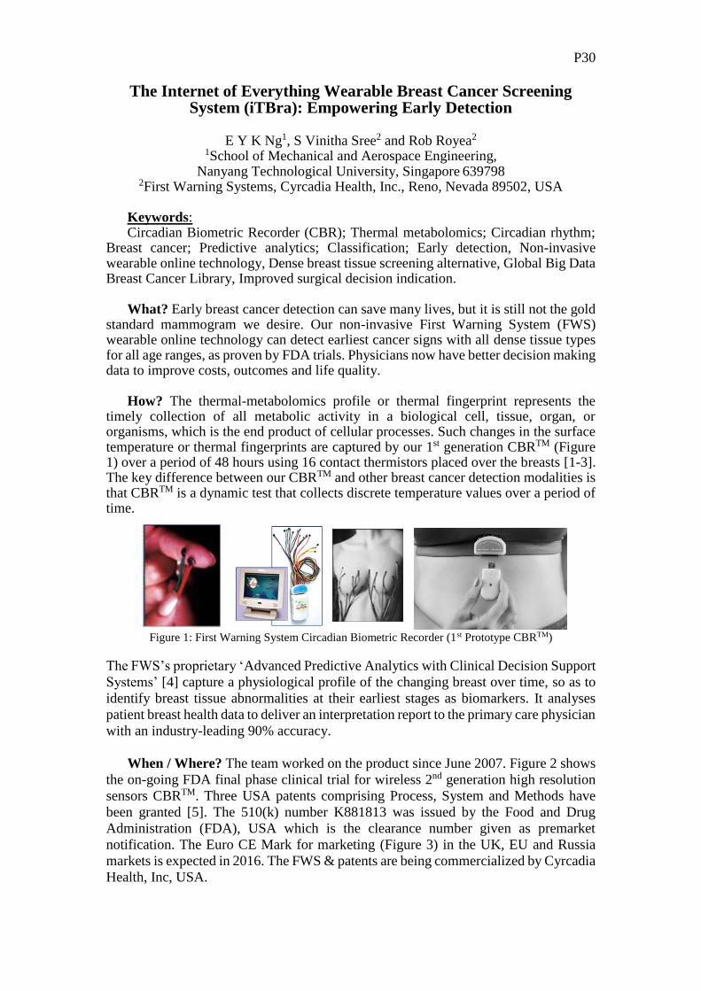
P30
The Internet of Everything Wearable Breast Cancer Screening System (iTBra): Empowering Early Detection
E Y K Ng1, S Vinitha Sree2 and Rob Royea2 1School of Mechanical and Aerospace Engineering,
Nanyang Technological University, Singapore 639798 2First Warning Systems, Cyrcadia Health, Inc., Reno, Nevada 89502, USA
Keywords: Circadian Biometric Recorder (CBR); Thermal metabolomics; Circadian rhythm;
Breast cancer; Predictive analytics; Classification; Early detection, Non-invasive wearable online technology, Dense breast tissue screening alternative, Global Big Data Breast Cancer Library, Improved surgical decision indication.
What? Early breast cancer detection can save many lives, but it is still not the gold standard mammogram we desire. Our non-invasive First Warning System (FWS) wearable online technology can detect earliest cancer signs with all dense tissue types for all age ranges, as proven by FDA trials. Physicians now have better decision making data to improve costs, outcomes and life quality.
How? The thermal-metabolomics profile or thermal fingerprint represents the
timely collection of all metabolic activity in a biological cell, tissue, organ, or organisms, which is the end product of cellular processes. Such changes in the surface temperature or thermal fingerprints are captured by our 1st generation CBRTM (Figure 1) over a period of 48 hours using 16 contact thermistors placed over the breasts [1-3]. The key difference between our CBRTM and other breast cancer detection modalities is that CBRTM is a dynamic test that collects discrete temperature values over a period of time.
Figure 1: First Warning System Circadian Biometric Recorder (1st Prototype CBRTM)
The FWS’s proprietary ‘Advanced Predictive Analytics with Clinical Decision Support
Systems’ [4] capture a physiological profile of the changing breast over time, so as to
identify breast tissue abnormalities at their earliest stages as biomarkers. It analyses
patient breast health data to deliver an interpretation report to the primary care physician
with an industry-leading 90% accuracy.
When / Where? The team worked on the product since June 2007. Figure 2 shows
the on-going FDA final phase clinical trial for wireless 2nd generation high resolution
sensors CBRTM. Three USA patents comprising Process, System and Methods have
been granted [5]. The 510(k) number K881813 was issued by the Food and Drug
Administration (FDA), USA which is the clearance number given as premarket
notification. The Euro CE Mark for marketing (Figure 3) in the UK, EU and Russia
markets is expected in 2016. The FWS & patents are being commercialized by Cyrcadia
Health, Inc, USA.

P31
Figure 2: On-going FDA Trial for 2nd generation wireless CBRTM
In sum: We use data mining (WRUBAC) techniques on the multidimensional time
series dataset to predict benign and malignant cases. A generalized classification framework is developed and comprises: (a) a data pre-processing element, (b) a feature selection element, (c) a classifier development element, and (d) a classifier evaluation element. FWS detects circadian cellular changes through thermal dynamic selection processes, allowing earlier, safer, and more accurate cancer prediction for women of all ages and tissue types, so as to reduce the number of necessary radiation procedures, while eliminating unnecessary surgeries.
Figure 3: Marketing Strategy upon FDA’s Approval
[1] Tan, JMY, Ng, E. Y.K., R Acharya U, Keith, L.G., and Holmes, J., “Comparative
Study on the use of Analytical Software to Identify the Different Stages of Breast
Cancer using Discrete Temperature Data”, Journal of Medical Systems, 2009, 3(2),
141-153. (DOI: 10.1007/s10916-008-9174-4)
[2] Ng, E. Y.K., R Acharya U, Keith, L.G., and Lockwood, S., “Detection and
Classification of Breast Cancer using Neural Classifiers with First Warning
Thermal Sensors”, Information Sciences, 2007, 177(20), 4526-4538. Selected
abstract for "Communications in Computer and Information Science" (2009).
[3] Ng E.Y.K., Tan MS, Lockwood S, Keith LG, ANN based Classification of Breast
Cancer with Discrete Temperature Screening: Facts and Myths, pp. 403-439. Chp.
21, Book Chapters in Emerging Technologies in Breast Imaging and
Mammography, J.S. Suri, R.M. Rangayyan and S Laxminarayan (Eds.), American
Scientific Publishers, USA, ISBN: 1-58883-090-X2008, 2006.
[4] S Vinitha Sree, Ng, E.Y.K., R Acharya U, and Jim Holmes “Evaluation of First
Warning Systems Circadian Biometric RecorderTM, a wearable breast cancer
detection device - A Predictive Analytics Paradigm”, Applied Soft Computing, (in-
press)

P32
[5] Three Granted US Patents No: 8,185,485 B2: Method/Process (2008); 8,231,542
B2: Utility: System (2012) and 8,226,572 B2: Utility: Methods (2012)

Special Thanks to
Analytical Technologies Pte Ltd
Bruker Singapore Pte Ltd
Leica Microsystems
Nanoscale Horizons
Raith Nanofabrication
WITec GmbH
Wiley