optimizing fpga-based cnn accelerator for energy ffi with an
TRANSCRIPT

Turk J Elec Eng & Comp Sci
(2018) 26: 919 – 935
c⃝ TUBITAK
doi:10.3906/elk-1706-222
Turkish Journal of Electrical Engineering & Computer Sciences
http :// journa l s . tub i tak .gov . t r/e lektr ik/
Research Article
Optimizing FPGA-based CNN accelerator for energy efficiency with an extended
Roofline model
Sayed Omid AYAT∗, Mohamed KHALIL-HANI, Ab Al-Hadi AB RAHMANVeCAD Research Laboratory, Faculty of Electrical Engineering, Universiti Teknologi Malaysia, Skudai,
Johor, Malaysia
Received: 20.06.2017 • Accepted/Published Online: 26.12.2017 • Final Version: 30.03.2018
Abstract: In recent years, the convolutional neural network (CNN) has found wide acceptance in solving practical
computer vision and image recognition problems. Also recently, due to its flexibility, faster development time, and
energy efficiency, the field-programmable gate array (FPGA) has become an attractive solution to exploit the inherent
parallelism in the feedforward process of the CNN. However, to meet the demands for high accuracy of today’s practical
recognition applications that typically have massive datasets, the sizes of CNNs have to be larger and deeper. Enlargement
of the CNN aggravates the problem of off-chip memory bottleneck in the FPGA platform since there is not enough space
to save large datasets on-chip. In this work, we propose a memory system architecture that best matches the off-chip
memory traffic with the optimum throughput of the computation engine, while it operates at the maximum allowable
frequency. With the help of an extended version of the Roofline model proposed in this work, we can estimate memory
bandwidth utilization of the system at different operating frequencies since the proposed model considers operating
frequency in addition to bandwidth utilization and throughput. In order to find the optimal solution that has the best
energy efficiency, we make a trade-off between energy efficiency and computational throughput. This solution saves
18% of energy utilization with the trade-off having less than 2% reduction in throughput performance. We also propose
to use a race-to-halt strategy to further improve the energy efficiency of the designed CNN accelerator. Experimental
results show that our CNN accelerator can achieve a peak performance of 52.11 GFLOPS and energy efficiency of 10.02
GFLOPS/W on a ZYNQ ZC706 FPGA board running at 250 MHz, which outperforms most previous approaches.
Key words: Convolutional neural network, field-programmable gate array, energy efficiency, Roofline model, race-to-halt
strategy.
1. Introduction
A convolutional neural network (CNN) is a neural network variant that provides one of the most accurate
approaches in the pattern recognition area [1]. Its ability to learn by mimicking the behavior of the brain’s
visual cortex makes it ideal for handling nonlinear problems. It has been applied in numerous applications such
as monitoring and surveillance, autonomous robot vision, and smart camera technologies [2–5].
Since inherent parallelism in the CNN cannot be fully exploited with the conventional CPU, many
researchers have proposed CNN accelerators for implementation in the field-programmable gate array (FPGA),
graphics processing unit (GPU) [6], and application-specific integrated circuit (ASIC) [7]. Recently, the FPGA
has been shown to be an alternative solution to accelerate CNN classification since it can exploit its inherent
∗Correspondence: [email protected]
919

AYAT et al./Turk J Elec Eng & Comp Sci
parallelism. However, the increment in the size of datasets and the model complexity of the CNN required
to meet the ever-growing demands of today’s practical applications makes on-chip memory inadequate to hold
this large amount of data. This means that the problem of off-chip memory bottleneck has to be critically
considered in the design of high-performance reconfigurable accelerators.
For an accelerator to achieve the maximum throughput possible, it needs to run at its maximum allowable
frequency. However, when operating at higher clock rates, the issue of memory bottleneck arises. The challenge
here is to match the memory traffic with the optimal throughput of the computation engine while operating at
its highest permitted frequency.
As opposed to the ASIC platform, the FPGA has the advantage of reconfigurability and fast development
time. In addition, studies have shown that FPGA accelerators can provide better energy utilization than CPUs
and GPUs [8]. Therefore, it is very important to study the power and energy usage of FPGA accelerators,
especially when implementing a computationally intensive and consequently power-hungry algorithm like a
CNN, targeted for power-constrained embedded devices.
Previous methods for power saving in embedded systems primarily concentrated on dynamic power loss,
whereas static energy dissipation was overlooked. In the meantime, the static power has grown drastically with
the decrease in the size of transistor technology [9]. In this work, energy efficiency is optimized by applying the
race-to-halt (RTH) mechanism proposed in [10] that reduces static power consumption.
In parallel processing platforms (FPGA and GPU), computational throughput is directly proportional
to energy efficiency [11]. In the FPGA platform, on the other hand, increasing both the degree of parallelism
and operating frequency in order to achieve higher throughput results in higher power consumption as well [8].
Therefore, there is also potentially a negative impact on the energy efficiency of the design when increasing the
throughput. Consequently, it is quite a challenging task to find the best degree of parallelism in the design of
an FPGA accelerator.
The main contributions of this research are as follows. First, we propose an extended version of the
Roofline model that, in addition to bandwidth utilization and throughput, also takes into consideration the
operating frequency of the computation engine. We use this extended roofline model to estimate the memory
bandwidth utilization and throughput of the system at different operating frequencies. An efficient memory
hierarchy architecture is also designed that can provide a data rate equal to the accelerator’s maximum
throughput while it runs at its maximum allowable frequency. This operating frequency is significantly higher
than the operating frequencies reported in literature. Secondly, the best trade-off between energy efficiency
and throughput is found by exploring the degrees of parallelism via board-level emulation. The RTH strategy
is applied to enhance the energy utilization in the CNN accelerator. Finally, benchmarking results show that
the proposed design, in terms of energy efficiency, outperforms most previous works while maintaining high
computation throughput.
The remainder of this paper is organized as follows: Section 2 outlines related works and introduces the
background information. The proposed models are presented in Section 3. Sections 4 and 5 are devoted to
the system development. Experimental results are analyzed in Section 6. Section 7 compares the results with
previous works and Section 8 draws conclusions.
2. Literature review
2.1. Previous related work
Most previous work on CNN accelerators mainly focused on computation engine optimization without consid-
ering the memory bandwidth limitation effect on the engine throughput [2,3]. The work by Peemen et al. [12],
920

AYAT et al./Turk J Elec Eng & Comp Sci
however, took the opposite approach and optimized just the memory bandwidth. Hence, these accelerators are
therefore either communication- or computation-bounded. This problem was solved by Zhang et al. [13], where
they used the Roofline analytical model proposed in [14] to match the memory bandwidth with the computation
throughput. The work by Zhang et al. can be further improved since they underutilized the available bandwidth
— using only 2.2 GB/s out of 4.5 GB/s bandwidth available — by running the computation engine at 100 MHz.
Energy efficiency is also becoming more crucial, especially in the real-time recognition of objects in
power-constrained autonomous systems and robots [4]. In an effort to design a CNN hardware accelerator
that is energy-efficient, [15] proposed an FPGA cluster to accelerate each layer of the network independently.
However, drawbacks of the work are the large board-to-board communication overhead and additional energy
utilization of an extra FPGA solely used for the purpose of controlling the remaining FPGAs.
There are two well-established methods to save on energy in embedded devices, and they are dynamic
voltage and frequency scaling (DVFS) [16] and the RTH mechanism [10]. Integrated circuits are recently
equipped with a number of sleep-state features. These features are mainly based on RTH, which can be used
to optimize the energy efficiency of the system. RTH enables the system to execute the task at high frequency,
hence completing it quickly and allowing the hardware to be turned off earlier [17]. DVFS, on the contrary,
decreases the operating frequency and therefore allows the circuit to operate at a lower voltage. Consequently,
DVFS minimizes dynamic energy dissipation with the sacrifice of static energy loss while RTH does completely
the reverse.
2.2. The CNN algorithm
A CNN consists of two main distinct processes: learning and testing (classification). Learning depends on both
feedforward and backward paths while the testing process is only executed in the feedforward path. In real-world
applications, what is vital for end users is the speed of classification. Hence, most previous works have proposed
CNN accelerators to perform the task of testing (classification) rather than learning [15]. Figure 1 shows the
AlexNet model, a CNN architecture that won the ImageNet contest in 2012 [6]. This CNN architecture is
adopted in this work. AlexNet is composed of five convolutional layers, three max-pooling layers, and three
fully connected layers. Since 90% of the computation time is consumed in the convolutional layers [13], in
this work, we will accelerate only the convolutional layers. Algorithm 1 given below is the algorithm of a
convolutional layer in the CNN. In this layer, to generate one pixel in each of the M output feature maps (FM),
N input feature maps are convolved with K ×K kernels that slide over the input feature maps.
Figure 1. Architecture of CNN in [6].
921

AYAT et al./Turk J Elec Eng & Comp Sci
Algorithm 1 Convolutional layer in CNN [13].
1: for ( row = 0 ; row < R ; row ++ ) {2: for ( col = 0 ; col < C ; col ++ ) {3: for ( to = 0 ; to < M ; to ++ ) {4: for ( ti = 0 ; ti < N ; ti ++ ) {5: for ( i= 0 ; i < K ; i++ ) {6: for (j= 0 ; j < K ; j ++ ) {7: Output FM [to] [row ] [col ] + =
8: Weights [to] [ti ] [i ] [j ] ×9: Input FM [ti ] [row +i ] [col +j ] ;
10: }}}}}}
2.3. Roofline model
The Roofline model as shown in Figure 2 was introduced in [14] for GPU and CPU platforms. It relates the
attainable system performance (i.e. throughput of the computation engine) to off-chip memory bandwidth (i.e.
data access rate from DRAM). Let CTC be the ratio of computation to communication, i.e. the amount of
operations per one byte of data accessed from the main (off-chip) memory, and let BW be the I/O memory
bandwidth, i.e. data access rate of the off-chip memory in bytes per second. Then the Roofline model is
formulated as follows:
Figure 2. Roofline model [14].
Attainable performance = min {Computational roof, CTC × BW} (1)
By this model, all possible legal design solutions are below the I/O bandwidth roof and the computational roof.
It is noted that the nominal data transfer rate (bandwidth) required for each solution is given by the gradient
of the line between any point (a design solution) and the origin point of the graph.
3. Proposed models
3.1. Extended Roofline model
The original Roofline model [14] was built upon the structure of a multicore system, in which the system
frequency is fixed. We propose an extended version of the Roofline model by including frequency (f) in its
922

AYAT et al./Turk J Elec Eng & Comp Sci
formulation as a tunable parameter. This is because, unlike GPU, the operating frequency of the FPGA
accelerator can be adjusted accordingly. In the proposed model, we compute the computational roof and the
off-chip memory bandwidth roof as follows, where T is the clock period, and f (=1/T) is the operating frequency.
Computational roof (operations per second) =Number of operations (operations)
Execution time (s)
=Num. of operations (operations)
Cycle count × T (s)(2)
=Num. of operations (operations)
Cycle count× f (Hz)
Memory BW (bytes per second) =Total bus width (bytes)
T (s)= Total bus width (bytes) × f (Hz) (3)
Hence, the proposed extended version of the Roofline model can be formulated as given by the following equation:
Attainable performance = Min
{(Num. of operations
Cycle count× f
), (CTC × Total bus width × f )
}(4)
Where: f ≤ Frequency wall
The above equations imply that changing the operating frequency alters the whole scenario in the original
model. Note that operating frequency of the design is directly proportional to the computational roof and
it also affects the required bandwidth. Hence, including f in the formulation of the original roofline model
provides the hardware designer with a better understanding of how the operating frequency impacts the
attainable throughput and memory bandwidth. Figure 3a provides a 3-dimensional (3D) view of the proposed
extended version of the Roofline model. Its difference from the original model is the inclusion of the so-called
frequency wall. All possible legal design solutions should be placed inside this “tent-like” 3D plot bounded
by the computational roof, memory bandwidth roof, and frequency wall. From this model we can extract, for
example, the performance of two design solutions with different operating frequencies. Figure 3b illustrates the
2-dimensional (2D) view of this model. Point A in this figure gives our expected performance at the maximum
frequency of 250 MHz (or frequency wall), while point B shows the peak performance achieved in the work done
in [13]. Figure 3b shows that at point B the computation engine is operating at a frequency as low as 100 MHz.
This corresponds to the situation where the available bandwidth is underutilized; that is, only 2.2 GB/s out of
4.5 GB/s bandwidth available is utilized. Our extended Roofline model will be used to improve this situation
by optimizing the clock rate and consequently the memory bandwidth utilization.
3.2. Energy utilization
Previous research [11] showed that power consumption can be calculated by the following equation, where
PStatic is static power due to transistor leakage currents and PDynamic is dynamic power due to the switching
activity of load capacitance:
PTotal = PStatic + PDynamic (5)
923

AYAT et al./Turk J Elec Eng & Comp Sci
(a) (b)
Figure 3. Extended Roofline model: a) 3- dimensional (3D), b) 2-dimensional (2D).
Dynamic power is directly proportional to the frequency (f) and has a quadratic relation to the voltage (V )
[11]; hence, it is defined by the following equation:
PDynamic = α × C × V 2 × f (6)
For an FPGA, capacitance (C) is determined by the amount of logic utilized within a configured hardware. The
variable α is the toggle rate of a component and is closely associated with the layout structure. Static power is
dependent on the temperature (T ) and, unlike dynamic power, it has no correlation to the utilized FPGA area
[11].
The device energy utilization is calculated based on its power consumption during a specific time interval
as defined in Eq. (7).
Energy (J) = Power (W ) × Execution time (s) =P (W ) × Cycle count (cycle)
f (Hz)(7)
Let EStatic and EDynamic be energy spent on static and dynamic power, respectively. From Eqs. (5),
(6), and (7), we can derive the equation for computing the total energy utilization in an FPGA:
ETotal = EStatic + EDynamic (8)
ETotal =PStatic × Cycle count
f+
PDynamic × Cycle count
f
=PStatic × Cycle count
f+ (α × C × V 2 × Cycle count) (9)
Eq. (9) implies several interesting points. The first point is that a shorter execution time (cycle count) of a
program has more effect on energy efficiency than reducing the resources (since capacitance (C) is proportional
to resource utilization). This is because a reduction in execution time can reduce both EStatic and EDynamic
while minimizing C can only improve EDynamic . That is the reason why in this work the first step we take is
924

AYAT et al./Turk J Elec Eng & Comp Sci
to maximize the throughput by using as many resources as we have (maximum degree of parallelism) and then,
in the following step, we apply an energy-throughput trade-off evaluation to find the solution with reduced
resource utilization. The second point is that we can predict that the design will have better energy efficiency
at higher frequencies because the effect of static energy is less at higher frequencies.
The abovementioned points imply the benefit of applying the RTH strategy for the FPGA. With RTH,
the system executes the task at high frequency, thus allowing for earlier completion in the interest of turning
off the hardware [17]. In this work, we apply the RTH strategy to improve the energy efficiency of the system.
4. CNN accelerator design
Based on the discussion in previous sections, to implement an energy-efficient CNN accelerator on an FPGA that
complies with the RTH mechanism, we need to find the best degree of parallelism and also run our system at its
maximum allowable operating frequency. To facilitate the high-frequency implementation of such a system, first
we use the analytical model discussed in Section 3.1, which takes into account operating frequency as well as
computation and memory bandwidth limitations. Second, we apply the energy-efficiency computation explained
in Section 3.2, which is based on degree of parallelism and operating frequency specified by RTH. Third, we
design a memory hierarchy infrastructure, presented in Section 5, which enables the accelerator system to access
the off-chip data at the maximum operating frequency.
Figure 4 shows the top-level functional block diagram of the proposed CNN accelerator system, which is
based on the work in [13]. Essentially the system is made up of two major components: the computation engine
and the memory hierarchy architecture. The memory hierarchy consists of on-chip buffers, data transfer engines
(DTEs), and a DRAM controller. Via the Xilinx Vivado High-Level Synthesis (HLS) design suite (v2015.4), all
IPs (including HLS IPs) are integrated into one single ZYNQ ZC706 FPGA chip.
In previous works [13,18], only the convolutional layers were accelerated in the hardware. This is
because 90% of the whole computation time is consumed in these layers. In this work, we also use the same
principle. Therefore, software/hardware (SW/HW) partitioning is done as follows: the hardware only executes
the convolutional layer and the software takes care of the rest of the algorithm. The software also controls the
BUS timings and the HW interrupts. The main focus of this paper is the hardware acceleration of convolutional
layers since it is the most computationally intensive part of the CNN algorithm.
In design exploration of the proposed CNN accelerator, we identify the following optimization goals.
The first goal is to find the CTC ratio with the maximum degree of parallelism that will result in the highest
computation throughput, regardless of the high power consumption that these solutions may have. This is in
accordance with the RTH strategy that insists on the higher degree of parallelism to finish the algorithm earlier,
rather than using fewer resources to consume less power. Therefore, the throughput of the circuit has higher
priority over resource utilization of the design for energy efficiency purposes in the FPGA. The second goal then
is to find the most energy-efficient solution among those that have been identified in the previous step. For the
second goal, our approach is to analyze the run-time power consumption and apply frequency scaling on each
selected solution via board-level emulation of the designs.
In order to control the CTC ratio, loop tiling is used to fit (i.e. cache in) a small segment of data to
on-chip memory. The CTC ratio is proportional to the unrolling factor or tile size. Algorithm 2 gives the
tiled convolutional layer in CNN [12]. Loop iterators row, col, to, and ti are tiled into loops with specific tile
sizes defined as Tm, Tn, Tr, and Tc. Unrolled loops are implemented via tree-shaped multiply-accumulator
processing elements (PEs) in the data-path unit (DU) of the computation engine, as depicted in Figure 4.
925

AYAT et al./Turk J Elec Eng & Comp Sci
Figure 4. Functional block diagram of CNN accelerator.
The PE is replicated Tm times, and these PEs execute in parallel with Tn inputs of input feature maps and
coefficients. Optimum throughput is achieved by pipelining this data-path structure.
Given a specific tile size combination Tm, Tn, Tr, Tc, the computational performance and CTC can be
calculated. From Eq. (2), we can predict that the computational roof of our accelerator is a function of Tm,
Tn, and also the frequency, f .
Computational roof of CNN accelerator (operation per second) =2×R× C ×M ×N ×K ×K
MTm × N
Tn × RTr × C
Tc × (Tr × Tc×K ×K)
× f = 2× Tm× Tn× f (10)
926

AYAT et al./Turk J Elec Eng & Comp Sci
Algorithm 2 Tiled convolutional layer in CNN [13].
1: Off-Chip Communication (...) {2: for ( row = 0 ; row < R ; row + = Tr ) {3: for ( col = 0 ; col < C ; col + = Tc ) {4: for ( to = 0 ; to < M ; to + = Tm ) {5: for ( ti = 0 ; ti < N ; ti + = Tn ) {6: On-Chip Computation (...) {7: for ( i = 0 ; i < K; i++){8: for ( j = 0 ; j < K; j ++){9: for ( trr = 0 ; trr < Tr ; trr ++){
10: for ( tcc = 0 ; tcc < Tc ; tcc ++){11: # pragma HLS PIPELINE
12: for ( too = 0 ; too < Tm ; too ++){13: # pragma HLS UNROLL
14: for ( tii = 0 ; tii < Tn ; tii ++){15: # pragma HLS UNROLL
16: Output FM [too] [trr] [tcc] + =
17: Weights [too] [tii] [i] [j] ×18: Input FM [tii] [trr + i] [tcc +j];
19: }}}}}}20: }21: }}}}22: }
CTC describes the computation operations per memory access. The CTC of the CNN accelerator in Algorithm
2 can be calculated by Eq. (11), where αin αwght, αout and βin, βwght βout are the numbers of load/unload
process and buffer capacity of input/output data and coefficients, correspondingly:
CTC of CNN accelerator =Total number of operations
Total number of external data access in bytes
=2 × R × C × M × N × K × K
αin × βin + αwght × βwght + αout × βout(11)
Taking into account the RTH strategy in our design space exploration, we look for design solutions that provide
maximum throughput although these solutions may consume much more power. Based on Eqs. (10) and (11),
incorporating the RTH strategy and also taking into account the resources available on our ZC706 FPGA board,
we derive the required degrees of parallelism (unrolling factors or tile sizes) to be:
Tm × Tn = 128 (12)
From the above equation, we obtain the possible solutions, labeled solution A to G as shown in Figure 5. Table
1 gives the corresponding unrolling factor for each solution. Solutions A to G are chosen such that the whole
927

AYAT et al./Turk J Elec Eng & Comp Sci
range of CTC ratios is covered so as to cover the complete range of all possible unrolling factors. Figure 5 shows
these solutions on the Roofline model and their expected performances.
CTC0 10 20 30 40 50
Att
ain
able
Per
form
ance
(F
LO
PS)
× 1010
0
1
2
3
4
5
6
7
8Tm=64
Tn=2
Tm=16
Tn=8
Tm=32
Tn=4Tm=128
Tn=1
Tm=2
Tn=64
Tm=8
Tn=16
Sol CSol B
Sol A
Sol E
Sol FSol D
Sol G
Computation Roof(F=250 MHz)
Communication Roof
Tm=4
Tn=32
Figure 5. Expected performance of all possible solutions at 250 MHz.
In this work, since the critical path delay (cpd) of our PE is 4 ns (given by the Vivado timing analysis
report), the frequency wall in our extended Roofline model is set at 1/4 ns = 250 MHz since the maximum
allowable operating frequency of a design is equal to 1/cpd.
5. Proposed memory architecture
Our memory hierarchy consists of three levels, as illustrated in Figure 6. These levels are the DRAM controller,
memory subsystem (MS), and finally on-chip buffers. All data for processing are first stored in the DRAM
(external memory) due to on-chip resource limitations. Data are then cached by DTEs into on-chip buffers
before being fed to PEs as shown in Figure 6. To overlap the computation time with the communication
latency of data transfer between DTEs and PEs, the double buffering technique from [13] is adopted.
DTE IPs have been shown to have limited memory access in previous works. For example, the maximum
performance of these engines reported in [13] at 100 MHz is around 400 MB/s and at a frequency of 125 MHz
Figure 6. Memory hierarchy architecture.
928

AYAT et al./Turk J Elec Eng & Comp Sci
is less than 500 MB/s [19]. Based on Eq. (3), the required bandwidth for each 32-bit AXI interface of our
accelerator (which are input, output, and weights AXI interfaces) at its maximum frequency of 250 MHz is 1
GB/s. Therefore, we need in total 3 GB/s read and write memory bandwidth for the whole system to be able
to run at its highest permitted frequency of 250 MHz. Setting the frequency to 250 MHz and using 3 GB/s
bandwidth satisfies the boundaries of our extended roofline model.
To resolve the issue of limited memory access of the DTE, we use two DTE engines for each of the
three interfaces and therefore employ six engines for the whole system. Figure 6 presents the proposed memory
subsystem, which consists of a pair of DTEs that can provide the data stream at 250 MHz clock rate (equivalent
to bandwidth of 1 GB/s for 32-bit floating point data).
6. Experimental results
6.1. Computational throughput
Figure 7 shows the attained performance (computational throughput) for all possible designs running at different
operating frequencies on the ZYNQ board. The values are obtained from the timer module in programmable
logic (PL) and also the interrupt routines in the ARM processor. The figure indicates that designs with the
best performance are found at larger values of CTC ratio and operating at higher frequencies. The collected
results in this figure also comply with the proposed extended Roofline model as illustrated in Figure 3b. From
Figure 7 and Table 2, solution G operating at 250 MHz (frequency wall) is the design with the best throughput
achieved among all the design solutions (A to G). It should be noted that the numbers in Figure 7 represent
the overall performance of our accelerator averaged over all layers of the CNN.
CTC
0 10 20 30 40 50
Ach
ieve
d p
erfo
rman
ce (
FL
OP
S)
× 1010
0
1
2
3
4
5
6
7BW Roof
Comp Roof
250 MHz
200 MHz
166 MHz
100 MHz
50 MHz
GFE
D
C
B
A
Figure 7. Achieved performance.
6.2. Energy utilization
Using solution E as an example, Table 3 reports the detailed power information of the design, showing that 39%
of total FPGA power is consumed in the PL; this suggests that saving power in PL can lead to the better overall
energy efficiency of the complete accelerator system. The runtime power consumption of PL for each solution
under a different operating frequency is illustrated in From Figure 8. Figure 9 shows how the run-time power
in PL is measured via the power management bus (PMBus). Each experiment is repeated multiple times and
the obtained values are then averaged over the number of iterations. This is to make sure that the measured
data are accurate.
929

AYAT et al./Turk J Elec Eng & Comp Sci
Table 1. Possible solutions.
Tm Tn
Solution A 2 64
Solution B 4 32
Solution C 8 16
Solution D 16 8
Solution E 32 4
Solution F 64 2
Solution G 128 1
Table 2. Achieved performance for solution G running at 250 MHz.
CNN Layer Latency (ms) Throughput (GFLOPS)
Layer 1 8.97 23.5
Layer 2 7.19 62.3
Layer 3 5.04 59.4
Layer 4 3.63 61.7
Layer 5 2.54 58.8
Overall 27.36 53.1
Table 3. Power consumption for solution E running at 250 MHz.
Power source Power (W)
PL 2.03
Auxiliary circuit 1.20
DDR3 domain 0.98
Board power net 0.17
Board components 0.21
Processor logic 0.45
Processor I/O 0.16
Total power 5.20
In previous works, a general-purpose power meter was used to measure the power consumption in an
FPGA. However, this method of measuring power takes into account the power consumed by the power adapter,
on-board DC voltage regulators, and also the FPGA circuitry. Hence, we cannot observe and investigate the
power consumption of modules such as the DDR, processing system (PS), and PL separately [20]. For this
reason, we utilize the dedicated PMBus controller [20] in the ZYNQ ZC706 FPGA board to obtain more
accurate measurement of the run-time power and energy consumption. Via the PMBus controller, we can
monitor the power utilization of each module on the FPGA board.
From Figure 8, it is observed that the run-time power consumption in our FPGA accelerator is almost
directly proportional to the operating frequency, as required by Eq. (9). Figure 8 also shows that higher
values of the CTC ratio, which correspond to enlarging the size of the hardware design, result in higher power
930

AYAT et al./Turk J Elec Eng & Comp Sci
CTC
0 10 20 30 40 50
Po
wer
co
nsu
mp
tio
n i
n P
L (
Wat
t)
1
1.5
2
2.5250 MHz
200 MHz
166 MHz
100 MHz
50 MHz
GF
ED
C
BA
Figure 8. Runtime power consumption (in PL). Figure 9. An example of run-time power measurement in
PL using PMBus.
consumption. Resource utilization of each solution is reported in Table 4, which indicates that as we increase
the intensity (CTC) of the algorithm, the BRAM, LUT, and FF utilization will also increase.
Table 4. Resource utilization of different solutions.
DSP BRAM LUT FF
Available 900 1090 218K 437K
Solution A 24% 23% 34% 14%
Solution B 36% 17% 35% 14%
Solution C 71% 14% 38% 17%
Solution D 71% 13% 39% 17%
Solution E 71% 14% 39% 17%
Solution F 73% 17% 44% 22%
Solution G 73% 22% 48% 28%
Figure 10 indicates that higher frequency can lead to better energy efficiency, which complies with RTH.
From Figure 10, by choosing solution E over G (which was chosen earlier), we save 18% of energy utilization
with the trade-off having less than 2% reduction in throughput performance. Consequently, solution E, with
the unrolling factors of Tm = 32 and Tn = 4, is our optimal solution that exhibits the best energy efficiency.
7. Benchmarking
In general, a comprehensive comparison with previous works is not possible due to different FPGA platforms
employed. Since the recent trend in high-performance computing is towards system-on-chip (SoC) implemen-
tation, the proposed CNN accelerator is implemented on the ZYNQ ZC706 FPGA SoC platform. For fair
comparison then, we benchmark our design against previous work that implemented a CNN in a SoC platform,
a design environment having a processor and dedicated hardware logic that is fabricated all on the same tech-
nology, 28-nm CMOS. The same test application, i.e. object classification with the ImageNet database [6], is
applied in all these benchmarking cases.
Table 5 gives the result of the benchmarking. As shown in this table, the proposed CNN accelerator
outperforms previous works in terms of energy efficiency (GFLOPS/W). The work by Zhang et al. [15] achieved
931
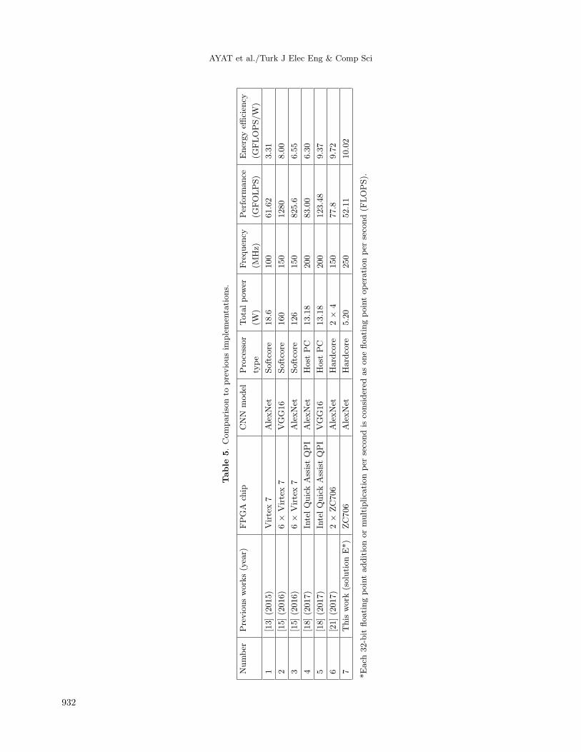
AYAT et al./Turk J Elec Eng & Comp Sci
Table
5.Comparisonto
previousim
plemen
tations.
Number
Previousworks(year)
FPGA
chip
CNN
model
Processor
Totalpow
erFrequen
cyPerform
ance
Energyeffi
cien
cy
type
(W)
(MHz)
(GFOLPS)
(GFLOPS/W
)
1[13](2015)
Virtex7
AlexNet
Softcore
18.6
100
61.62
3.31
2[15](2016)
6×
Virtex7
VGG16
Softcore
160
150
1280
8.00
3[15](2016)
6×
Virtex7
AlexNet
Softcore
126
150
825.6
6.55
4[18](2017)
IntelQuickAssistQPI
AlexNet
Host
PC
13.18
200
83.00
6.30
5[18](2017)
IntelQuickAssistQPI
VGG16
Host
PC
13.18
200
123.48
9.37
6[21](2017)
2×
ZC706
AlexNet
Hardcore
2×
4150
77.8
9.72
7This
work
(solutionE*)
ZC706
AlexNet
Hardcore
5.20
250
52.11
10.02
*Each
32-bit
floatingpointadditionormultiplicationper
secondis
considered
asonefloatingpointoperationper
second(F
LOPS).
932

AYAT et al./Turk J Elec Eng & Comp Sci
CTC0 10 20 30 40 50
En
ergy
E!
icie
ncy
(F
LO
P/J
)
× 1013
0
0.5
1
1.5
2
250 MHz
200 MHz
166 MHz
100 MHz
50 MHz
GFE
D
C
BA
Figure 10. Energy efficiency.
the highest throughput at the expense of resource utilization (they used 7 FPGA boards). However, their design
has lower energy efficiency due to the unavoidable board-to-board communication overhead and also energy loss
from the extra FPGA board that was only used as a master to control other FPGAs. The accelerator in [13]
spent a considerable amount of dynamic power on employing a softcore processor since the FPGA board was
not equipped with the hardcore PS. In the case of the design in [18], the FPGA is connected to the PC and
uses the host CPU as a main processor. However, the power analysis did not consider the power consumption
of the host CPU.
Our accelerator can run at a higher frequency compared to others due to the optimized bandwidth
utilization found in this work. Applying the RTH strategy and working out the throughput-energy trade-offs
results in attaining an energy efficiency of 10.02 (GFLOPS/W) for the proposed CNN accelerator.
8. Conclusions
The following conclusions can be drawn from this study: first, based on our extended Roofline model, in
designing an FPGA accelerator we have to consider another restrictive element in our analytical performance
estimation, which is the frequency wall. Operating frequency can affect two other limiting factors, namely
bandwidth utilization and computational roof. Second, we show that in today’s FPGA platforms the RTH
strategy can be considered as a high-level technique to improve the energy efficiency of a design. To achieve
higher energy efficiency based on this methodology, the throughput of the circuit has more priority over the
resource utilization of the design. If we do not use the available resources then they incur a penalty on energy
utilization since these unused logics also consume a considerable amount of static power. The third major
finding in our CNN accelerator architecture is that the degree of parallelism in the innermost loops of the CNN
algorithm (unrolling factors Tm and Tn in this work) plays a very important role in the determination of
throughput, BW utilization, and also the energy efficiency of our design, and therefore should be considered
carefully.
Acknowledgment
This work was supported by Universiti Teknologi Malaysia (UTM) and the Ministry of Science, Technology,
and Innovation of Malaysia (MOSTI) under ScienceFund Grant No. 4S116.
933
AYAT et al./Turk J Elec Eng & Comp Sci
References
[1] Parisa Beham M, Mohamed S, Roomi M. A review of face recognition methods. Int J Pattern Recogn 2013; 27:
1-35.
[2] Farabet C, Poulet C, Han JY, LeCun Y. CNP: An FPGA-based processor for convolutional networks. In: Interna-
tional Conference on Field Programmable Logic and Applications; 31 August 2009; Prague, Czech Republic. New
York, NY, USA: IEEE. pp. 32-37.
[3] Sankaradas M, Jakkula V, Cadambi S, Chakradhar S, Durdanovic I, Cosatto E, Graf HP. A massively parallel
coprocessor for convolutional neural networks. In: IEEE International Conference on Application-specific Systems,
Architectures and Processors; 7 July 2009; Boston, MA, USA. New York, NY, USA: IEEE. pp. 53-60.
[4] Hadsell R, Sermanet P, Ben J, Erkan A, Scoffier M, Kavukcuoglu K, Muller U, LeCun Y. Learning long-range vision
for autonomous off-road driving. J Field Robot 2009; 26: 120-144.
[5] Maria J, Amaro J, Falcao G, Alexandre LA. Stacked autoencoders using low-power accelerated architectures for
object recognition in autonomous systems. Neural Process Lett 2016; 43: 445-458.
[6] Krizhevsky A, Sutskever I, Hinton GE. ImageNet classification with deep convolutional neural networks. In:
Advances in Neural Information Processing Systems; 3–8 December 2012; Nevada, USA. pp. 1097-1105.
[7] Han S, Liu X, Mao H, Pu J, Pedram A, Horowitz MA, Dally WJ. EIE: Efficient inference engine on compressed
deep neural network. In: Proceedings of the 2016 International Symposium on Computer Architecture; 18–22 June
2016; Seoul, Republic of Korea. New York, NY, USA: IEEE. pp. 243-254.
[8] Buyukkurt B, Guo Z, Najjar W. Impact of loop unrolling on area, throughput and clock frequency in ROCCC: C
to VHDL compiler for FPGAs. Lect Notes Comp Sci 2006; 3985: 401-412.
[9] Kim NS, Austin T, Baauw D, Mudge T, Flautner K, Hu JS, Irwin MJ, Kandemir M, Narayanan V. Leakage current:
Moore’s law meets static power. Computer 2003; 36: 68-75.
[10] Awan MA, Petters SM. Race-to-halt energy saving strategies. J Syst Architect 2014; 60: 796-815.
[11] Jamieson P, Luk W, Wilton SJ, Constantinides GA. An energy and power consumption analysis of FPGA routing
architectures. In: 2009 International Conference on Field-Programmable Technology; 9–11 December 2009; Sydney,
Australia. New York, NY, USA: IEEE. pp. 324-327.
[12] Peemen M, Setio AA, Mesman B, Corporaal H. Memory-centric accelerator design for convolutional neural networks.
In: 2013 IEEE International Conference on Computer Design; 6–9 October 2013; North Carolina, USA. New York,
NY, USA: IEEE. pp. 13-19.
[13] Zhang C, Li P, Sun G, Guan Y, Xiao B, Cong J. Optimizing FPGA-based accelerator design for deep convolutional
neural networks. In: 2015 ACM/SIGDA International Symposium on Field-Programmable Gate Arrays; 22–24
February 2015; Monterey, CA, USA. New York, NY, USA: ACM. pp. 161-170.
[14] Williams S, Waterman A, Patterson D, Hall S, Berkeley UC. Roofline: an insightful visual performance model for
multicore architectures. Commun ACM 2009; 52: 65-76.
[15] Zhang C, Wu D, Sun J, Sun G, Luo G, Cong J. Energy-efficient CNN implementation on a deeply pipelined FPGA
cluster. In: Proceedings of the 2016 International Symposium on Low Power Electronics and Design; 8–10 August
2016; San Francisco, CA, USA. New York, NY, USA: ACM. pp. 326-331.
[16] Mantovani P, Cota EG, Tien K, Pilato C, Di Guglielmo G, Shepard K, Carlon LP. An FPGA-based infrastruc-
ture for fine-grained DVFS analysis in high-performance embedded systems. In: 2016 ACM/EDAC/IEEE Design
Automation Conference; 5–9 June 2016; Austin, TX, USA. New York, NY, USA: IEEE. pp. 1-6.
[17] Choi JW, Bedard D, Fowler R, Vuduc R. A roofline model of energy. In: 2013 IEEE International Parallel &
Distributed Processing Symposium; 20–24 May 2013; Boston, MA, USA. New York, NY, USA: IEEE. pp. 661-672.
[18] Zhang C, Prasanna VK. Frequency domain acceleration of convolutional neural networks on CPU-FPGA shared
memory system. In: 25th ACM/SIGDA International Symposium on Field-Programmable Gate Arrays; 22–24
February 2017; Monterey, CA, USA. New York, NY, USA: ACM. pp. 35-44.
934

AYAT et al./Turk J Elec Eng & Comp Sci
[19] Sadri M, Weis C, Wehn N, Benini L. Energy and performance exploration of accelerator coherency port using Xilinx
ZYNQ. In: Proceedings of 10th FPGA World Conference; 10–12 September 2013; Stockholm, Sweden. New York,
NY, USA: ACM. p. 5.
[20] Beldachi AF, Nunez-Yanez JL. Accurate power control and monitoring in ZYNQ boards. In: 2014 International
Conference on Field Programmable Logic and Applications; 2–4 September 2014; Munich, Germany. New York,
NY, USA: IEEE. pp. 1-4.
[21] Qiao Y, Shen J, Xiao T, Yang Q, Wen M, Zhang C. FPGA-accelerated deep convolutional neural networks for high
throughput and energy efficiency. Concurr Comp-Pract E 2017; 29: 1-20.
935