optimal design of a cmos op-amp via geometric …boyd/papers/pdf/opamp_tcad.pdf · index terms—...
TRANSCRIPT

IEEE TRANSACTIONS ON COMPUTER-AIDED DESIGN OF INTEGRATED CIRCUITS AND SYSTEMS, VOL. 20, NO. 1, JANUARY 2001 1
Optimal Design of a CMOS Op-Amp via GeometricProgramming
Maria del Mar Hershenson, Stephen P. Boyd, Fellow, IEEE, and Thomas H. Lee
Abstract—We describe a new method for determining com-ponent values and transistor dimensions for CMOS operationalamplifiers (op-amps). We observe that a wide variety of designobjectives and constraints have a special form, i.e., they areposyn-omial functions of the design variables. As a result, the amplifierdesign problem can be expressed as a special form of optimizationproblem called geometric programming, for which very efficientglobal optimizationmethods have been developed. As a consequencewe can efficiently determine globally optimal amplifier designsor globally optimal tradeoffs among competing performancemeasures such as power, open-loop gain, and bandwidth. Ourmethod, therefore, yields completely automated sizing of (globally)optimal CMOS amplifiers, directly from specifications.
In this paper, we apply this method to a specific widely used op-erational amplifier architecture, showing in detail how to formu-late the design problem as a geometric program. We compute glob-ally optimal tradeoff curves relating performance measures such aspower dissipation, unity-gain bandwidth, and open-loop gain. Weshow how the method can be used to sizerobust designs, i.e., de-signs guaranteed to meet the specifications for a variety of processconditions and parameters.
Index Terms—Circuit optimization, CMOS analog integratedcircuits, design automation, geometric programming, mixedanalog–digital integrated circuits, operational amplifiers.
I. INTRODUCTION
A S THE demand for mixed-mode integrated circuits in-creases, the design of analog circuits such as operational
amplifiers (op-amps) in CMOS technology becomes more crit-ical. Many authors have noted the disproportionately large de-sign time devoted to the analog circuitry in mixed-mode inte-grated circuits. In this paper, we introduce a new method for de-termining the component values and transistor dimensions forCMOS op-amps. The method handles a very wide variety ofspecifications and constraints, isextremely fast, and results inglobally optimaldesigns.
The performance of an op-amp is characterized by a numberof performance measures such as open-loop voltage gain,quiescent power, input-referred noise, output voltage swing,unity-gain bandwidth, input offset voltage, common-moderejection ratio, slew rate, die area, and so on. These perfor-mance measures are determined by the design parameters,e.g., transistor dimensions, bias currents, and other componentvalues. The CMOS amplifier design problem we consider in
Manuscript received November 10, 1997; revised March 9, 2000. This paperwas recommended by Associate Editor K. Mayalam.
M. del Mar Hershenson is with Barcelona Design, Inc., Sunnyvale, CA 94086USA.
S. P. Boyd and T. H. Lee are with the Electrical Engineering Department,Stanford University, Stanford, CA 94305 USA.
Publisher Item Identifier S 0278-0070(01)00348-7.
this paper is to determine values of the design parameters thatoptimize an objective measure while satisfying specificationsor constraints on the other performance measures. This designproblem can be approached in several ways, e.g., by hand ora variety of computer-aided-design methods, e.g., classicaloptimization methods, knowledge-based methods or simulatedannealing. (These methods are described more fully below.)
In this paper, we introduce a new method that has a numberof important advantages over current methods. We formulate theCMOS op-amp design problem as a very special type of opti-mization problem called ageometric program. The most im-portant feature of geometric programs is that they can be refor-mulated asconvex optimization problemsand, therefore,glob-ally optimal solutions can be computed withgreat efficiency,even for problems with hundreds of variables and thousands ofconstraints, using recently developed interior-point algorithms.Thus, even challenging amplifier design problems with manyvariables and constraints can be (globally) solved.
The fact that geometric programs (and, hence, CMOS op-ampdesign problems cast as geometric programs) can be globallysolved has a number of important practical consequences. Thefirst is that sets of infeasible specifications are unambiguouslyrecognized: the algorithms either produce a feasible point ora proof that the set of specifications is infeasible. Indeed, thechoice of initial design for the optimization procedure is com-pletely irrelevant (and can even be infeasible); it has no effect onthe final design obtained. Since the global optimum is found, theop-amps obtained are not just the best our method can design, butin fact the bestanymethod can design (with the same specifica-tions). In particular, our method computes theabsolute limit ofperformancefor a given amplifier and technology parameters.
The fact that geometric programs can be solved very effi-ciently has a number of practical consequences. For example,the method can be used to simultaneously optimize the designof a large number of op-amps in a single large mixed-mode inte-grated circuit. In this case, the designs of the individual op-ampsare coupled by constraints on total power and area, and by var-ious parameters that affect the amplifier coupling such as inputcapacitance, output resistance, etc. Another application is to usethe efficiency to obtainrobust designs, i.e., designs that are guar-anteed to meet a set of specifications over a variety of processesor technology parameter values. This is done by simply repli-cating the specifications with a (possibly large) number of rep-resentative process parameters, which is practical only becausegeometric programs with thousands of constraints are readilysolved.
All the advantages mentioned (convergence to a global so-lution, unambiguous detection of infeasibility, sensitivity anal-
0278–0070/01$10.00 © 2001 IEEE

2 IEEE TRANSACTIONS ON COMPUTER-AIDED DESIGN OF INTEGRATED CIRCUITS AND SYSTEMS, VOL. 20, NO. 1, JANUARY 2001
Fig. 1. Two-stage op-amp considered herein.
ysis, …) are due to the formulation of the design problem as aconvexoptimization problem. Geometric programming (whenreformulated as described in Section II-A) is just a special typeof convex optimization problem. Although general convex prob-lems can be solved efficiently, the special structure of geometricprogramming can be exploited to obtain an even more efficientsolution algorithm.
The method we present can be applied to a wide variety ofamplifier architectures, but in this paper, we apply the methodto a specific two-stage CMOS op-amp. The authors show howthe method extends to other architectures in [49] and [50]. Alonger version of this paper, which includes more detail aboutthe models, some of the derivations, and SPICE simulationparameters, is available at the authors’ web site [51]. Relatedwork has been reported in several conference publications, e.g.,[48]–[50].
A. The Two-Stage Amplifier
The specific two-stage CMOS op-amp we consider is shownin Fig. 1. The circuit consists of an input differential stage withactive load followed by a common-source stage also with ac-tive load. An output buffer is not used; this amplifier is as-sumed to be part of a very large scale integration (VLSI) systemand is only required to drive a fixed on-chip capacitive load ofa few picofarads. This op-amp architecture has many advan-tages: high open-loop voltage gain, rail-to-rail output swing,large common-mode input range, only one frequency compen-sation capacitor, and a small number of transistors. Its maindrawback is the nondominant pole formed by the load capac-itance and the output impedance of the second stage, whichreduces the achievable bandwidth. Another potential disadvan-tage is the right half-plane zero that arises from the feedforwardsignal path through the compensating capacitor. Fortunately, thezero is easily removed by a suitable choice for the compensationresistor (see [2]).
This op-amp is a widely used general purpose op-amp [88];it finds applications, for example, in switched capacitor filters[23], analog-to-digital converters [60], [72], and sensing circuits[85].
There are 18 design parameters for the two-stage op-amp:
• The widths and lengths of all transistors, i.e.,and .
• The bias current .• The value of the compensation capacitor.
The compensation resistor is chosen in a specific way that isdependent on the design parameters listed above (and describedin Section V). There are also a number of parameters that weconsider fixed, e.g., the supply voltages and , the ca-pacitive load , and the various process and technology pa-rameters associated with the MOS models. To simplify some ofthe equations we assume (without any loss of generality) that
.
B. Other Approaches
There is a huge literature, which goes back more than 20years, on computer-aided design (CAD) of analog circuits. Agood survey of early research can be found in the survey [11];more recent papers on analog-circuit CAD tools include [4],[12], [13]. The problem we consider in this paper, i.e., selectionof component values and transistor dimensions, is only a part ofa complete analog-circuit CAD tool. Other parts, which we donot consider here, include topology selection (see [66]) and ac-tual circuit layout (see, e.g., ILAC [27], KOAN/ANAGRAM II[15]). The part of the CAD process that we consider lies betweenthese two tasks; the remainder of the discussion is restricted tomethods dealing with component and transistor sizing.
1) Classical Optimization Methods:General-purpose clas-sical optimization methods, such as steepest descent, sequen-tial quadratic programming, and Lagrange multiplier methods,have been widely used in analog-circuit CAD. These methodscan be traced back to the survey paper [11]. The widely usedgeneral-purpose optimization codes NPSOL [39] and MINOS[71] are used in [25], [64], and [67]. LANCELOT [16], an-other general-purpose optimizer, is used in [22]. Other CADapproaches based on classical optimization methods, and exten-sions such as a minimax formulation, include the one describedin [47], [61], and [63], OAC [78], OPASYN [56], CADICS [54],WATOPT [31], and STAIC [45]. The classical methods can beused with more complicated circuit models, including even fullSPICE simulations in each iteration, as in DELIGHT.SPICE[75] (which uses the general-purpose optimizer DELIGHT [76])and ECSTASY [86].
The main advantage of these methods is the wide variety ofproblems they can handle; the only requirement is that the per-formance measures, along with one or more derivatives, can becomputed. The main disadvantage of the classical optimizationmethods is they only findlocally optimaldesigns. This meansthat the design is at least as good as neighboring designs, i.e.,small variations of any of the design parameters results in aworse (or infeasible) design. Unfortunately this does not meanthe design is the best that can be achieved, i.e., globally optimal;it is possible (and often happens) that some other set of designparameters, far away from the one found, is better. The sameproblem arises in determining feasibility: a classical (local) op-timization method can fail to find a feasible design, even thoughone exists. Roughly speaking, classical methods can get stuck atlocal minima. This shortcoming is so well known that it is oftennot even mentioned in papers; it is taken as understood.
The problem of nonglobal solutions from classical optimiza-tion methods can be treated in several ways. The usual approach

DEL MAR HERSHENSONet al.: OPTIMAL DESIGN OF A CMOS OP-AMP VIA GEOMETRIC PROGRAMMING 3
is to start the minimization method from many different ini-tial designs, and to take the best final design found. Of course,there are no guarantees that the globally optimal design has beenfound; this method merely increases the likelihood of finding theglobally optimal design. This method also destroys one of theadvantages of classical methods, i.e., speed, since the computa-tion effort is multiplied by the number of different initials de-signs that are tried. This method also requires human interven-tion (to give “good” initial designs), which makes the methodless automated.
The classical methods become slow if complex models areused, as in DELIGHT.SPICE, which requires more than a com-plete SPICE run at each iteration (“more than” since, at the least,gradients must also be computed).
2) Knowledge-Based Methods:Knowledge-based andexpert-systems methods have also been widely used in analogcircuit CAD. Examples include genetic algorithms or evolutionsystems like SEAS [74], DARWIN [58], [100]; systems basedon fuzzy logic like FASY [46] and [92]; special heuristics-basedsystems like IDAC [29], [30], OASYS [44], BLADES [21],and KANSYS [43].
One advantage of these methods is that there are few limita-tions on the types of problems, specifications, and performancemeasures that can be considered. Indeed, there are even fewerlimitations than for classical optimization methods since manyof these methods do not require the computation of derivatives.
These methods have several disadvantages. They find a lo-cally optimal design (or, even just a “good” or “reasonable” de-sign) instead of a globally optimal design. The final design de-pends on the initial design chosen and the algorithm parameters.As with classical optimization methods, infeasibility is not un-ambiguously detected; the method simply fails to find a feasibledesign (even when one may exist). These methods require sub-stantial human intervention either during the design process, orduring the training process.
3) Global Optimization Methods:Optimization methodsthat are guaranteed to find the globally optimal design have alsobeen used in analog-circuit design. The most widely knownglobal optimization methods are branch and bound [103] andsimulated annealing [94], [101].
A branch and bound method is used, e.g., in [66]. Branchand bound methods unambiguously determine the globally op-timal design: at each iteration they maintain a suboptimal fea-sible design and also a lower bound on the achievable perfor-mance. This enables the algorithm to terminate nonheuristically,i.e., with complete confidence that the global design has beenfound within a given tolerance. The disadvantage of branch andbound methods is that they are extremely slow, with computa-tion growing exponentially with problem size. Even problemswith 10 variables can be extremely challenging.
Simulated annealing (SA) is another very popular methodthat can avoid becoming trapped in a locally optimal design.In principle it can compute the globally optimal solution, butin implementations there is no guarantee at all, since, for ex-ample, the cooling schedules called for in the theoretical treat-ments are not used in practice. Moreover, no real-time lowerbound is available, so termination is heuristic. Like classicaland knowledge-based methods, SA allows a very wide variety
of performance measures and objectives to be handled. Indeed,SA is extremely effective for problems involving continuousvariables and discrete variables, as in, e.g., simultaneous am-plifier topology and sizing problems. SA has been used in sev-eral tools such as ASTR/OBLX [77], OPTIMAN [38], FRIDGE[68], SAMM [105], and [14].
The main advantages of SA are that it handles discrete vari-ables well, and greatly reduces the chances of finding a nonglob-ally optimal design. (Practical implementations do not reducethe chance to zero, however.) The main disadvantage is that itcan be very slow, and cannot (in practice) guarantee a globallyoptimal solution.
4) Convex Optimization and Geometric ProgrammingMethods: In this section, we describe the general optimizationmethod we employ in this paper: convex optimization. Theseare special optimization problems in which the objective andconstraint functions are all convex.
While the theoretical properties of convex optimization prob-lems have been appreciated for many years, the advantages inpractice are only beginning to be appreciated now. The mainreason is the development of extremely powerful interior-pointmethods for general convex optimization problems in the lastfive years (e.g., [73] and [102]). These methods can solve largeproblems, with thousands of variables and tens of thousands ofconstraints, very efficiently (in minutes on a small workstation).Problems involving tens of variables and hundreds of constraints(such as the ones we encounter in this paper) are consideredsmall, and can be solved on a small current workstation in lessthan one second. The extreme efficiency of these methods is oneof their great advantages.
The other main advantage is that the methods are trulyglobal, i.e., the global solution isalways found, regardlessof the starting point (which, indeed, need not be feasible).Infeasibility is unambiguously detected, i.e., if the methodsdo not produce a feasible point they produce a certificate thatproves the problem is infeasible. Also, the stopping criteria arecompletely nonheuristic: at each iteration a lower bound on theachievable performance is given.
One of the disadvantages is that the types of problems, perfor-mance specifications, and objectives that can be handled are farmore restricted than any of the methods described above. Thisis the price that is paid for the advantages of extreme efficiencyand global solutions. (For more on convex optimization, and theimplications for engineering design, see [10].)
The contribution of this paper is to show how to formulatethe analog amplifier design problem as a certain type of convexproblem called geometric programming. The advantages, com-pared to the approaches described above, are extreme efficiencyand global optimality. The disadvantage is less flexibility inthe types of constraints we can handle, and the types of circuitmodels we can employ.
Aside from work we describe below, the only other appli-cation of geometric programming to circuit design is in tran-sistor and wire sizing for Elmore delay minimization in digitalcircuits, as in TILOS [36] and other programs [81], [82], [87].Their use of geometric programming can be distinguished fromours in several ways. First of all, the geometric programs thatarise in Elmore delay minimization are very specialized (the
4 IEEE TRANSACTIONS ON COMPUTER-AIDED DESIGN OF INTEGRATED CIRCUITS AND SYSTEMS, VOL. 20, NO. 1, JANUARY 2001
only exponents that arise are 0 and). Second, the problemsthey encounter in practice are extremely large, involving up tohundreds of thousands of variables. Third, their representationof the problem as a geometric program is quite an approxima-tion, since the actual circuits are nonlinear, and the thresholddelay, not Elmore delay, is the true objective.
Convex optimization is mentioned in several papers onanalog-circuit CAD. The advantages of convex optimizationare mentioned in [65] and [66]. In [25] and [26], the authors usea supporting hyperplane method, which they point out providesthe global optimum if the feasible set is convex. In [89], theauthors optimize a few design variables in an op-amp using aLagrange multiplier method, which yields the global optimumsince the small subproblems considered are convex. In [95] and[96], convex optimization is used to optimize area, power, anddominant time constant in digital circuit wire and transistorsizing.
During the review process for this paper, the authors wereinformed of similar work that had been submitted to IEEETRANSACTIONS ONCOMPUTER-AIDED DESIGN OFINTEGRATED
CIRCUITS AND SYSTEMS by Mandal and Visvanathan [24].Mandal and Visvanathan show how geometric programmingcan be used to size another simple op-amp, and describe asimple method for iteratively refining monomial device models.
C. Outline of Paper
In Section II, we briefly describe geometric programming, thespecial type of optimization problem at the heart of the method,and show how it can be cast as a convex optimization problem.In Sections III–VI we describe a variety of constraints and per-formance measures, and show that they have the special formrequired for geometric programming. In Section VII we givenumerical examples of the design method, showing globallyoptimal tradeoff curves among various performance measuressuch as bandwidth, power, and area. We also verify some of ourdesigns using high fidelity SPICE models, and briefly discusshow our method can be extended to handle short-channel ef-fects. In Section IX, we discuss robust design, i.e., how to usethe methods to ensure proper circuit operation under variousprocessing conditions. In Section X, we give our concluding re-marks.
II. GEOMETRIC PROGRAMMING
Let be real, positive variables. We will denotethe vector of these variables as. A function iscalled aposynomialfunction of if it has the form
where and . Note that the coefficients mustbe nonnegative, but the exponents can be any real num-bers, including negative or fractional. When there is exactly onenonzero term in the sum, i.e., and , we call amonomialfunction. (This terminology is not consistent with thestandard definition of a monomial in algebra, but it should notcause any confusion.) Thus, for example, is
posynomial (but not monomial); is a monomial(and, therefore, also a posynomial); while is nei-ther. Note that posynomials are closed under addition, multipli-cation, and nonnegative scaling. Monomials are closed undermultiplication and division.
A geometric programis an optimization problem of the form
minimize
subject to
(1)
where are posynomial functions and aremonomial functions.
Several extensions are readily handled. Ifis a posynomialand is a monomial, then the constraint canbe handled by expressing it as (since isposynomial). For example, we can handle constraints of theform , where is posynomial and . In a sim-ilar way if and are both monomial functions, then we canhandle the equality constraint by expressing itas (since is monomial).
We will also encounter functions whose reciprocals areposynomials. We say is inverse posynomialif is aposynomial. If is an inverse posynomial and is a posyn-omial, then geometric programming can handle the constraint
by writing it as . As anotherexample, if is an inverse posynomial, then we can maximizeit, by minimizing (the posynomial) .
Geometric programming has been known and used since thelate 1960s, in various fields. There were two early books ongeometric programming, by Duffinet al. [18] and Zener [106],which include the basic theory, some electrical engineeringapplications (e.g., optimal transformer design), but not muchon numerical solution methods. Another book appeared in1976 [9]. The 1980 survey paper by Ecker [19] has manyreferences on applications and methods, including numericalsolution methods used at that time. Geometric programmingis briefly described in some surveys of optimization, e.g., [20,pp. 326–328] or [99, Ch. 4]. While geometric programming iscertainly known, it is nowhere near as widely known as, say,linear programming. In addition, advances in general-purposenonlinear constrained optimization algorithms and codes (suchas the ones described above) have contributed to decreased use(and knowledge) of geometric programming in recent years.
A. Geometric Programming in Convex Form
A geometric program can be reformulated as aconvexoptimization problem, i.e., the problem of minimizing a convexfunction subject to convex inequality constraints and linearequality constraints. This is the key to our ability to globally andefficiently solve geometric programs. We define new variables
, and take the logarithm of a posynomialto get

DEL MAR HERSHENSONet al.: OPTIMAL DESIGN OF A CMOS OP-AMP VIA GEOMETRIC PROGRAMMING 5
where and . It can be shown thatis aconvexfunction of the new variable: for all
and we have
Note that if the posynomial is a monomial, then the trans-formed function is affine, i.e., a linear function plus a constant.
We can convert the standard geometric program (1) into aconvex program by expressing it as
minimize
subject to
(2)
This is the so-calledconvex formof the geometric program (1).Convexity of the convex form geometric program (2) has sev-eral important implications: we can use efficient interior-pointmethods to solve them, and there is a complete and useful du-ality, or sensitivity theory for them; see, e.g., [10].
B. Solving Geometric Programs
Since Ecker’s survey paper, there have been several impor-tant developments, related to solving geometric programmingin the convex form. A huge improvement in computational ef-ficiency was achieved in 1994, when Nesterov and Nemirovskydeveloped efficient interior-point algorithms to solve a varietyof nonlinear optimization problems, including geometric pro-grams [73]. Recently, Kortaneket al.have shown how the mostsophisticated primal-dual interior-point methods used in linearprogramming can be extended to geometric programming, re-sulting in an algorithm approaching the efficiency of currentinterior-point linear programming solvers [57]. The algorithmthey describe has the desirable feature of exploitingsparsityinthe problem, i.e., efficiently handling problems in which eachvariable appears in only a few constraints. Other methods de-veloped specifically for geometric programs include those de-scribed by Avrielet al.[7] and Rajpogal and Bricker [80], whichrequire solving a sequence of linear programs (for which veryefficient algorithms are known).
The algorithms described above are specially tailored forthe geometric program (in convex form). It is also possible tosolve the convex form problem using general purpose opti-mization codes that handle smooth objectives and constraintfunctions, e.g., LANCELOT [16], MINOS [71], LOQO [97], orLINGO-NL [83]. These codes will (in principle) find a globallyoptimal solution, since the convex form problem is convex.They will also determine the optimal dual variables (sensitivi-ties) as a by-product of solving the problem. In an unpublishedreport [104], Xu compares the performance of the sophisticatedprimal-dual interior-point method developed by Kortaneketal.(XGP, [57]) with two general-purpose optimizers, MINOSand LINGO-NL, on a suite of standard geometric programmingproblems (in convex form). The general-purpose codes fail tosolve some of the problems, and in all cases take substantiallylonger to obtain the solution.
For our purposes, the most important feature of geometricprograms is that they can beglobally solved withgreat effi-
ciency. Problems with hundreds of variables and thousands ofconstraints are readily handled, on a small workstation, in min-utes; the problems we encounter in this paper, which have onthe order of ten variables and 100 constraints, are easily solvedin under one second.
To carry out the designs in this paper, we implemented, inMATLAB, a simple and crude primal barrier method for solvingthe convex form problem. Roughly speaking, this method con-sists of applying a modified Newton’s method to minimizing thesmooth convex function
subject to the affine (linear equality) constraints, , for an increasing
sequence of values of, starting from the optimal found forthe last value of . It can be shown that when , theoptimal solution of this problem is no more thansuboptimalfor the original convex form geometric program (GP). Thecomputational complexity of this simple method is ,where is the number of variables, andis the total numberof terms in monomials and posynomials in the objective andconstraints. For much more detail, see [10] and [35].
Despite the simplicity of the algorithm (i.e., primal only, withno sparsity exploited) and the overhead of an interpreted lan-guage, the geometric programs arising in this paper were allsolved in approximately 1 or 2 s on an ULTRA SPARC1 runningat 170 MHz. Since our simple interior-point method is alreadyextremely fast on the relatively small problems we encounterin this paper, we feel that the choice of algorithm is not critical.When the method is applied to large-scale problems, such as theones obtained for a robust design problem (see Section IX), thechoice may well become critical.
C. Sensitivity Analysis
Suppose we modify the right-hand sides of the constraints inthe geometric program (1) as follows:
minimize
subject to
(3)
If all of the and are zero, this modified geometric pro-gram coincides with the original one. If , then the con-straint represents atightenedversion of the orig-inal th constraint ; conversely if , it repre-sents alooseningof the constraint. Note that gives a loga-rithmic or fractional measure of the change in the specification:
means that theth constraint is loosened 10%,whereas means that theth constraint is tight-ened 10%.
Let denote the optimal objective value of the mod-ified geometric program (3), as a function of the parameters
and , so the original ob-jective value is . In sensitivity analysis, we study thevariation of as a function of and , for small and . To
6 IEEE TRANSACTIONS ON COMPUTER-AIDED DESIGN OF INTEGRATED CIRCUITS AND SYSTEMS, VOL. 20, NO. 1, JANUARY 2001
express the change in optimal objective function in a fractionalform, we use thelogarithmic sensitivities
(4)
evaluated at , . These sensitivity numbers aredimensionless, since they express fractional changes per frac-tional change.
For simplicity we are assuming here that the original geo-metric program is feasible, and remains so for small changesin the right-hand sides of the constraints, and also that the op-timal objective value is differentiable as a function ofand .More complete descriptions of sensitivity analysis in other casescan be found in the references cited above, or in a general con-text in [10]. The surprising part is that the sensitivity numbers
and come for free, when the problemis solved using an interior-point or Lagrangian-based method(from the solution of the dual problem; see [10]).
We start with some simple observations. If at the optimal so-lution of the original problem, theth inequality constraintis not active, i.e., is strictly less than one, then(since we can slightly tighten or loosen theth constraint withno effect). We always have since increasing slightlyloosens the constraints, and hence lowers the optimal objectivevalue. The sign of tells us whether increasing the right-handside side of the equality constraint increases or decreasesthe optimal objective value.
The sensitivity numbers are extremely useful in practice, andgive tremendous insight to the designer. Suppose, for example,that the objective is power dissipation, repre-sents the constraint that the bandwidth is at least 30 MHz, and
represents the constraint that the open-loop gain isV V. Then , say, tells us that a small fractional
increase in required bandwidth will translate into a three timeslarger fractional increase in power dissipation. tellsus that a small fractional increase in required open-loop gainwill translate into a fractional increase in power dissipation onlyone-tenth as big. Although both constraints are active, the sensi-tivities tell us that the design is, roughly speaking, more tightlyconstrained by the bandwidth constraint than the open-loop gainconstraint. The sensitivity information from the example abovemight lead the designer to reduce the required bandwidth (to re-duce power), or perhaps increase the open-loop gain (since itwould not cost much). We give an example of sensitivity anal-ysis in Section VII-D.
III. D IMENSION CONSTRAINTS
We start by considering some very basic constraints involvingthe device dimensions, e.g., symmetry, matching, minimum ormaximum dimensions, and area limits.
A. Symmetry and Matching
For the intended operation of the input differential pair, tran-sistors and must be identical and transistors andmust also be identical. These conditions translate into the fourequality constraints
(5)
The biasing transistors , , and must match, i.e., havethe same length
(6)
The six equality constraints in (5) and (6) have monomialexpressions on the left- and right-hand sides and hence, arereadily handled in geometric programming (by expressingthem as monomial equality constraints such as ).
Note that (5) and (6) effectively reduce the number of vari-ables from 18 to 12. We can, for example, eliminate the variables
and by substituting wherever they appear. For clarity,we will continue to use the variables and in our discus-sion; for computational purposes, however, they can be replacedby . (In any case, the number of variables and constraints isso small for a geometric program that there is almost no com-putational penalty in keeping the extra variables and equalityconstraints.)
B. Limits on Device Sizes
Lithography limitations and layout rules impose minimum(and possibly maximum) sizes on the transistors
(7)
These 32 constraints can be expressed as posynomial constraintssuch as , etc. Since and are variables(hence, monomials), we can also fix certain devices sizes, i.e.,impose equality constraints.
We should note that a constraint limiting device dimensionsto a finite number of allowed values, or to an integer multiple ofsome fixed small value,cannotbe (directly) handled by geo-metric programming. Such constraints can be approximatelyhandled by simple rounding to an allowed value, or using moresophisticated mixed convex-integer programming methods.
C. Area
The op-amp die area can be approximated as a constantplus the sum of transistor and capacitor area as
(8)
Here gives the fixed area, is the ratio of capacitorarea to capacitance, and the constant (if it is not one)can take into account wiring in the drain and source area. Thisexpression for the area is a posynomial function of the designparameters, so we can impose an upper bound on the area, i.e.,
, or use the area as the objective to be minimized.This simple expresion does not take routing area into account;more accurate posynomial formulas for the amplifier die areacould be developed, if needed.
D. Systematic Input Offset Voltage
To reduce input offset voltage, the drain voltages of andmust be equal, ensuring that the currentis split equally

DEL MAR HERSHENSONet al.: OPTIMAL DESIGN OF A CMOS OP-AMP VIA GEOMETRIC PROGRAMMING 7
between transistors and . This happens when the currentdensities of , , and are equal, i.e.,
(9)
These two conditions are equality constraints between mono-mials, and are therefore readily handled by geometric program-ming.
IV. BIAS, CONDITIONS, SIGNAL SWING, AND POWER
CONSTRAINTS
In this section, we consider constraints involving bias condi-tions, including the effects of common-mode input voltage andoutput signal swing. We also consider the quiescent power of theop-amp (which is determined, of course, by the bias conditions).In deriving these constraints, we assume that the symmetry andmatching conditions (5) and (6) hold. To derive the equations,we use a standard long-channel square-law model for the MOStransistors, which is described in detail in the Appendix. Werefer to this model as the GP0 model; the same analysis alsoapplies to the more accurate GP1 model, also described in theAppendix.
In order to simplify the equations, it is convenient to definethe bias currents , , and through transistors , , and
, respectively. Transistors and form a current mirrorwith transistor . Their currents are given by
(10)
Thus and are monomials in the design variables. The cur-rent through transistor is split equally between transistorand . Thus, we have
(11)
which is another monomial.Since these bias currents are monomials, we can include
lower or upper bounds on them, or even equality constraints, ifwe wish. We will use , , and in order to express otherconstraints, remembering that these bias currents can simplybe eliminated (i.e., expressed directly in terms of the designvariables) using (10) and (11).
A. Bias Conditions
The setup for deriving the bias conditions is as follows. Theinput terminals are at the same dc potential, the common-modeinput voltage . We assume that the common-mode inputvoltage is allowed to range between a minimum valueand a maximum value , which are given. Similarly,we assume that the output voltage is allowed to swing betweena minimum value and a maximum value(which takes into account large signal swings in the output).
The bias conditions are that each transistorshould remain in saturation for all possible values of the inputcommon-mode voltage and the output voltage. The derivationof the bias constraints given below can be found in the longerreport [51]. The important point here is that the constraints
are each posynomial inequalities on the design variables and,hence, can be handled by geometric programming.
• Transistor . The lowest common-mode input voltageimposes the toughest constraint on transistor
remaining in saturation. The condition is
(12)
Note that if the right-hand side of (12) were negative, i.e.,if , then the design is imme-diately known to be infeasible (since the left-hand side is,of course, positive).
• Transistor . The systematic offset condition (9) makesthe drain voltage of equal to the drain voltage of .Therefore, the condition for being saturated is thesame as the condition for being saturated, i.e., (12).Note that the minimum allowable value of is de-termined by and entering the linear region.
• Transistor . Since transistor is alwaysin saturation and no additional constraint is necessary.
• Transistor . The systematic offset condition also im-plies that the drain voltage of is equal to the drainvoltage of . Thus, will be saturated as well.
• Transistor . The highest common-mode input voltage, imposes the tightest constraint on transistor
being in saturation. The condition is
(13)
Thus, the maximum allowable value of is de-termined by entering the linear region. As explainedabove, if the right-hand side of (13) is negative, i.e.,
, then the design is obviouslyinfeasible.
• Transistor . The most stringent condition occurs whenthe output voltage is at its minimum value
(14)
In this case the right-hand side of (14) will not be negativeif we assume the minimum output voltage is above thenegative supply voltage.
• Transistor . For , the most stringent condition oc-curs when the output voltage is at its maximum value
(15)
Here too, the right hand-side of (15) will be positive as-suming the maximum output voltage is below the positivesupply voltage.
• Transistor . Since , transistor is alwaysin saturation; no additional constraint is necessary.

8 IEEE TRANSACTIONS ON COMPUTER-AIDED DESIGN OF INTEGRATED CIRCUITS AND SYSTEMS, VOL. 20, NO. 1, JANUARY 2001
In summary, the requirement that all transistors remain insaturation for all values of common-mode input voltage be-tween and , and all values of output voltagebetween and , is given by the four inequalities(12)–(15). These are complicated, butposynomialconstraints onthe design parameters.
B. Gate Overdrive
It is sometimes desirable to operate the transistors with aminimum gate overdrive voltage. This ensures that they operateaway from the subthreshold region, and also improves matchingbetween transistors. For any given transistor this constraint canbe expressed as
(16)
The expression on the left is a monomial, so we can also imposean upper bound on it, or an equality constraint, if we wish. (Wewill see in Section IX that robustness to process variations canbe dealt with in a more direct way.)
C. Quiescent Power
The quiescent power of the op-amp is given by
(17)
which is a posynomial function of the design parameters. Hence,we can impose an upper bound onor use it as the objectiveto be minimized.
V. SMALL –SIGNAL TRANSFERFUNCTION CONSTRAINTS
A. Small-Signal Transfer Function
We now assume that the symmetry, matching, and bias con-straints are satisfied, and consider the (small-signal) transferfunction from a differential input source to the output. Toderive the transfer function , we use a standard small-signalmodel for the transistors, which is described in the Appendix,Section B. The standard value of the compensation resistor isused, i.e.,
(18)
(see [2]).The transfer function can be well approximated by a four-pole
form
(19)Here, is the open-loop voltage gain, is the dominantpole, is the output pole, is the mirror pole, and isthe pole arising from the compensation circuit. In order to sim-plify the discussion in the sequel, we will refer to ,which are positive, as the poles (whereas precisely speaking, thepoles are ).
We now give the expressions for the gain and poles. Thetwo-stage op-amp has been previously analyzed by many au-
thors [32], [53], [88]. The compensation scheme has also beenanalyzed previously, e.g., in [2].
• The open-loop voltage gain is
(20)
which is monomial function of the design parameters.• The dominant pole is accurately given by
(21)
Since and are monomials, and is a design vari-able, is a monomial function of the design variables.
• The output pole is given by
(22)
where , the capacitance at the gate of , can be ex-pressed as
(23)
and , the total capacitance at the output node, can beexpressed as
(24)
The meanings of these parameters, and their dependenceon the design variables, is given in the Appendix, Sec-tion B. The important point here is that is an inverseposynomial function of the design parameters (i.e.,is a posynomial).
• The mirror pole is given by
(25)
where , the capacitance at the gate of , can be ex-pressed as
(26)
Thus, is also an inverse posynomial.• The compensation pole is
(27)
which is also inverse posynomial.In summary: the open-loop gain and the dominant poleare monomial, and the parasitic poles, , and are all
inverse posynomials. Now we turn to various design constraintsand specifications that involve the transfer function.
B. Open-Loop Gain Constraints
Since the open-loop gain is a monomial, we can constrainit to equal some desired value . We could also impose upperor lower bounds on the gain, as in
(28)

DEL MAR HERSHENSONet al.: OPTIMAL DESIGN OF A CMOS OP-AMP VIA GEOMETRIC PROGRAMMING 9
where and are given lower and upper limits on ac-ceptable open-loop gain.
C. Minimum Gain at a Frequency
The magnitude squared of the transfer function at a frequencyis given by
Since are all inverse posynomial, the expressions areposynomial. Hence, the whole denominator is posynomial. Thenumerator is monomial, thus we conclude that the squared mag-nitude of the transfer function, , is inverse posyno-mial. (Indeed, it is inverse posynomial in the design variablesand as well.) We can, therefore, impose any constraint of theform
using geometric programming [by expressing it as].
The transfer function magnitude decreases as in-creases (since it has only poles), so is equivalentto
for (29)
We will see below that this allows us to specify a minimumbandwidth or crossover frequency.
D. 3-dB Bandwidth
The 3-dB bandwidth is the frequency at which the gaindrops 3 dB below the dc open-loop gain, i.e.,
. To specify that the 3-dB bandwidth is at least someminimum value , i.e., , is equivalentto specifying that . This is turn can beexpressed as
(30)
which is a posynomial inequality.In almost all designs will be the dominant pole, (see below)
so the 3-dB bandwidth is very accurately given by
(31)
which is a monomial. Using this (extremely accurate) approx-imation, we can constrain the 3-dB bandwidth to equal somerequired value. Using the constraint (30), which is exact but in-verse posynomial, we can constrain the 3-dB bandwidth to ex-ceed a given minimum value.
E. Dominant Pole Conditions
The amplifier is intended to operate with as the dominantpole, i.e., much smaller than , , and . These conditionscan be expressed as
(32)
where we (arbitrarily) use one decade, i.e., a factor of ten infrequency, as the condition for dominance. These dominantpole conditions are readily handled by geometric program-ming, since is monomial and , , and are all inverseposynomial. In fact these dominant pole conditions usuallydo not need to be included explicitly since the phase marginconditions described below are generally more strict, anddescribe the real design constraint. Nevertheless, it is commonpractice to impose a minimum ratio between the dominant andnondominant poles; see, e.g., [42].
F. Unity-Gain Bandwidth and Phase Margin
We define the unity-gain bandwidth as the frequency atwhich . The phase margin is defined in terms ofthe phase of the transfer function at the unity-gain bandwidth
PM
A phase margin constraint specifies a lower bound on the phasemargin, typically between – .
The unity-gain bandwidth and phase margin are related tothe closed-loop bandwidth and stability of the amplifier withunity-gain feedback, i.e., when its output is connected to theinverting input. If the op-amp is to be used in some otherspecific closed-loop configuration, then a different frequencywill be of more interest, but the analysis is the same. For ex-ample, if the op-amp is to be used in a feedback configurationwith closed-loop gain dB, then the critical frequency isthe 20-dB crossover point, i.e., the frequency at which theopen-loop gain drops to 20 dB, and the phase margin is definedat that frequency. All of the analysis below is readily adaptedwith minimal changes to such a situation. For simplicity, wecontinue the discussion for the unity-gain bandwidth.
We start by considering a constraint that the unity-gain band-width should exceed a given minimum frequency, i.e.,
(33)
This constraint is just a minimum gain constraint at the fre-quency [as in (29)], and, thus, can be handled exactlyby geometric programming as a posynomial inequality.
Here too we can develop an approximate expression for theunity-gain bandwidth which is monomial. If we assume the par-asitic poles , , and are at least a bit (say, an octave) abovethe unity-gain bandwidth, then the unity-gain bandwidth can beapproximated as the open-loop gain times the 3-dB bandwidth,i.e.,
(34)
which is a monomial. If we use this approximate expression forthe unity-gain bandwidth, we can fix the unity-gain bandwidthat a desired value. The approximation (34) ignores the decreasein gain due to the parasitic poles and, consequently, overesti-mates the actual unity-gain bandwidth (i.e., the gain drops to0 dB at a frequency slightly less than ).
We now turn to the phase margin constraint, for which we cangive a very accurate posynomial approximation. Assuming the
10 IEEE TRANSACTIONS ON COMPUTER-AIDED DESIGN OF INTEGRATED CIRCUITS AND SYSTEMS, VOL. 20, NO. 1, JANUARY 2001
open-loop gain exceeds ten or so, the phase contributed by thedominant pole at the unity-gain bandwidth, i.e., ,will be very nearly . Therefore, the phase margin constraintcan be expressed as
PM (35)
i.e., the nondominant poles cannot contribute more thanPM total phase shift.
The phase margin constraint (35) cannot be exactly handledby geometric programming, so we use two reasonable approxi-mations to form a posynomial approximation. The first is an ap-proximate unity-gain bandwidth [from (34)] insteadof the exact unity-gain bandwidth as the frequency at whichwe will constrain the phase of . As mentioned above, we have
, thus, our specification is a bit stronger than theexact phase margin specification (since we are constraining thephase at a frequency slightly above the actual unity gain band-width). We will also approximate as a monomial.A simple approximation is given by , which isquite accurate for less than . Thus, assuming thateach of the parasitic poles contributes no more than aboutof phase shift, we can approximate the phase margin constraintaccurately as
PM (36)
which is a posynomial inequality in the design variables (sinceis monomial). The approximation error involved here
is almost always very small for the following reasons. The con-straint (36) makes sure none of the nondominant poles is toonear . This, in turn, validates our approximation
. It also ensures that our approximation that the phase con-tributed by the nondominant poles is is good.
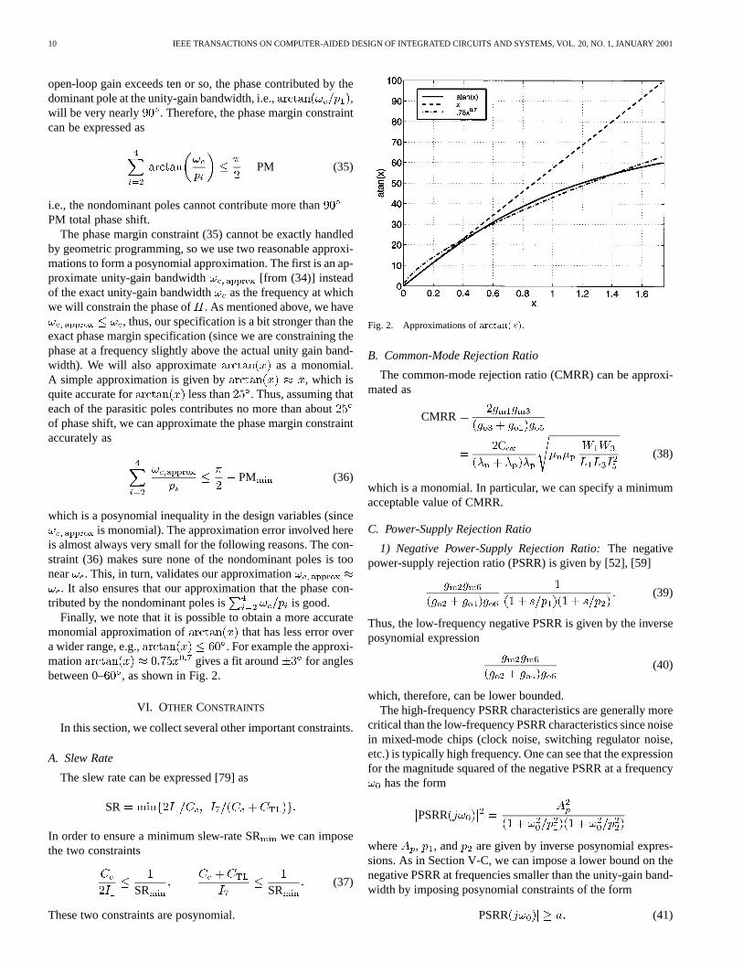
Finally, we note that it is possible to obtain a more accuratemonomial approximation of that has less error overa wider range, e.g., . For example the approxi-mation gives a fit around for anglesbetween 0– , as shown in Fig. 2.
VI. OTHER CONSTRAINTS
In this section, we collect several other important constraints.
A. Slew Rate
The slew rate can be expressed [79] as
SR
In order to ensure a minimum slew-rate SRwe can imposethe two constraints
SR SR(37)
These two constraints are posynomial.
Fig. 2. Approximations ofarctan(x).
B. Common-Mode Rejection Ratio
The common-mode rejection ratio (CMRR) can be approxi-mated as
CMRR
C(38)
which is a monomial. In particular, we can specify a minimumacceptable value of CMRR.
C. Power-Supply Rejection Ratio
1) Negative Power-Supply Rejection Ratio:The negativepower-supply rejection ratio (PSRR) is given by [52], [59]
(39)
Thus, the low-frequency negative PSRR is given by the inverseposynomial expression
(40)
which, therefore, can be lower bounded.The high-frequency PSRR characteristics are generally more
critical than the low-frequency PSRR characteristics since noisein mixed-mode chips (clock noise, switching regulator noise,etc.) is typically high frequency. One can see that the expressionfor the magnitude squared of the negative PSRR at a frequency
has the form
PSRR
where , , and are given by inverse posynomial expres-sions. As in Section V-C, we can impose a lower bound on thenegative PSRR at frequencies smaller than the unity-gain band-width by imposing posynomial constraints of the form
PSRR (41)

DEL MAR HERSHENSONet al.: OPTIMAL DESIGN OF A CMOS OP-AMP VIA GEOMETRIC PROGRAMMING 11
2) Positive Power-Supply Rejection Ratio:The low-fre-quency positive PSRR is given by
PSRR (42)
which is neither posynomial nor inverse-posynomial, thus, itfollows that constraints on the positive power supply rejectioncannot be handled by geometric programming. However, thisop-amp suffers from much worse negative PSRR characteris-tics than positive PSRR characteristics, both at low and highfrequencies [40], [42]. Therefore, not constraining the positivePSRR is not critical.
We must at the least check the positive PSRR of any designcarried out by the method described in this paper. (It is morethan adequate in every design we have carried out.) However,if the positive PSRR specification becomes critical, it can beapproximated (conservatively) by a posynomial inequality, e.g.,using Duffin linearization [7], [17].
D. Noise Performance
The equivalent input-referred noise power spectral density(in V /Hz, at frequency assumed smaller than the
3-dB bandwidth), can be expressed as
where is the input-referred noise power spectral density oftransistor . These spectral densities consist of the input-re-ferred thermal noise and a noise
Thus, the input-referred noise spectral density can be expressedas
where
Note that and are (complicated) posynomial functions ofthe design parameters.
We can, therefore, impose spot noise constraints, i.e., requirethat
(43)
for a certain , as a posynomial inequality. (We can impose mul-tiple spot noise constraints, at different frequencies, as multipleposynomial inequalities.)
TABLE IDESIGNCONSTRAINTS ANDSPECIFICATIONS FOR THETWO-STAGE OP-AMP
The total rms noise level over a frequency band(where is below the equivalent noise bandwidth of the circuit)can be found by integrating the noise spectral density:
Therefore, imposing a maximum total rms noise voltage overthe band is the posynomial constraint
(44)
(since and are fixed, and and are posynomials in thedesign variables).
VII. OPTIMAL DESIGN PROBLEMS AND EXAMPLES
A. Summary of Constraints and Specifications
The many performance specifications and constraints de-scribed in the previous sections are summarized in Table I.Note that with only one exception (the positive supply rejectionratio), the specifications and constraints can be handled viageometric programming.
Since all the op-amp performance measures and constraintsshown above can be expressed as posynomial functions andposynomial constraints, we can solve a wide variety of op-ampdesign problems via geometric programming. We can, for ex-ample, maximize the bandwidth subject to given (upper) limitson op-amp power, area, and input offset voltage, and given(lower) limits on transistor lengths and widths, and voltagegain, CMRR, slew rate, phase margin, and output voltageswing. The resulting optimization problem is a geometricprogramming problem. The problem may appear to be verycomplex, involving many complicated inequality and equalityconstraints, but in fact is readily solved.

12 IEEE TRANSACTIONS ON COMPUTER-AIDED DESIGN OF INTEGRATED CIRCUITS AND SYSTEMS, VOL. 20, NO. 1, JANUARY 2001
TABLE IISPECIFICATIONS ANDCONSTRAINTS FORDESIGN EXAMPLE
TABLE IIIOPTIMAL DESIGN FORDESIGN EXAMPLE
B. Example
In this section, we describe a simple design example. A 0.8m CMOS technology was used; see the longer report [51] for
more details and the technology parameters. The positive supplyvoltage was set at 5 V and the negative supply voltage was setat 0 V. The load capacitance was 3 pF.
The objective is to maximize unity-gain bandwidth subject tothe requirements shown in Table II. The resulting geometric pro-gram has 18 variables, seven (monomial) equality constraints,and 28 (posynomial) inequality constraints. The total number ofmonomial terms appearing in the objective and all constraints is68. Our simple MATLAB program solves this problem in underone second real-time. The optimal design obtained is shown inTable III.
The performance achieved by this design, as predicted by theprogram, is summarized in Table IV. The design achieves an86-MHz unity-gain bandwidth. Note that some constraints aretight (minimum device length, minimum device width, max-imum output voltage, quiescent power, phase margin and input-referred spot noise) while some constraints are not tight (area,minimum output voltage open-loop gain, common-mode rejec-tion ratio, and slew rate).
TABLE IVPERFORMANCE OFOPTIMAL DESIGN FORDESIGN EXAMPLE
C. Tradeoff Analyses
By repeatedly solving optimal design problems as we sweepover values of some of the constraint limits, we can sweep outglobally optimal tradeoff curves for the op-amp. For example,we can fix all other constraints, and repeatedly minimize poweras we vary a minimum required unity-gain bandwidth. Theresulting curve shows the globally optimal tradeoff betweenunity-gain bandwidth and power (for the values of the otherlimits).
In this section, we show several optimal tradeoff curves forthe operational amplifier. We do this by fixing all the specifica-tions at the default values shown in Table II, except two that wevary to see the effect on a circuit performance measure. Whenthe optimization objective is not bandwidth we use a defaultvalue of minimum unity-gain bandwidth of 30 MHz.
We first obtain the globally optimal tradeoff curve ofunity-gain bandwidth versus power for different supply volt-ages. The results can be seen in Fig. 3. Obviously the morepower we allocate to the amplifier, the larger the bandwidthobtained; the plots, however, show exactly how much morebandwidth we can obtain with different power budgets. We cansee, for example, that the benefits of allocating more powerto the op-amp disappear above 5 mW for a supply voltageof 2.5 V, whereas for a 5 V supply the bandwidth continuesto increase with increasing power. Note also that each of thesupply voltages gives the largest unity-gain bandwidth oversome range of powers.
In Fig. 4, we plot the globally optimal tradeoff curve ofopen-loop gain versus unity-gain frequency for different phasemargins. Note that for a large unity-gain bandwidth requirementonly small gains are achievable. Also, we can see that for atighter phase margin constraint the gain bandwidth product islower.
Fig. 5 shows the minimum input-referred spectral densityat 1 kHz versus power, for different unity-gain frequency re-quirements. Note that when the power specification is tight, in-creasing the power greatly helps to decrease the input-referrednoise spectral density.
In Fig. 6 we show the optimal tradeoff curve of unity-gainbandwidth versus area for different different power budgets.

DEL MAR HERSHENSONet al.: OPTIMAL DESIGN OF A CMOS OP-AMP VIA GEOMETRIC PROGRAMMING 13
Fig. 3. Maximum unity-gain bandwidth versus power for different supplyvoltages.
Fig. 4. Maximum open-loop gain versus unity-gain bandwidth for differentphase margins.
We can see that when the area constraint is tight, increasingthe available area translates into a greater unity bandwidth.After some point, other constraints become more stringent andincreasing the available area does not improve the maximumachievable unity-gain bandwidth.
Several other optimal tradeoff curves are given in the longerreport [51].
D. Sensitivity Analysis Example
In this section, we analyze the information provided by thesensitivity analysis of the first design problem in Section VII-B(maximize the unity-gain bandwidth when the rest of specifica-tions/constraints are set to the values shown in Table II). Theresults of this sensitivity analysis are shown in Table V. Thecolumn labeled “Sensitivity” (numerical) is obtained by tight-ening and loosening the constraint in question by 5% and re-solving the problem. (The average from the two is taken.) Thecolumn labeled “Sensitivity” comes (essentially for free) fromsolving the original problem. Note that it gives an excellent pre-diction of the numerically obtained sensitivities.
Fig. 5. Minimum noise density at 1 kHz versus power for different unity-gainbandwidths.
Fig. 6. Maximum unity-gain bandwidth versus area for different powerbudgets.
There are six active constraints: minimum device length, min-imum device width, maximum output voltage, quiescent power,phase margin, and input-referred spot noise at 1 kHz. All ofthese constraints limit the maximum unity-gain bandwidth. Thesensitivities indicate which of these constraints are more crit-ical (more limiting). For example, a 10% increase in the allow-able input-referred noise at 1 kHz will produce a design with(approximately) 2.4% improvement in unity-gain bandwidth.However, a 10% decrease in the maximum phase margin atthe unity-gain bandwidth will produce a design with (approxi-mately) 17.6% improvement in unity-gain bandwidth. It is veryinteresting to analyze the sensitivity to the minimum devicewidth constraint. A 10% decrease in the minimum device widthproduces a design with only a 0.05% improvement in unity-gainbandwidth. This can be interpreted as follows: even though theminimum device width constraint is binding, it can be consid-ered not binding in a practical sense since tightening (or loos-ening) it will barely change the objective.
The program classifies the given constraints in order of im-portance from most limiting to least limiting. For this design

14 IEEE TRANSACTIONS ON COMPUTER-AIDED DESIGN OF INTEGRATED CIRCUITS AND SYSTEMS, VOL. 20, NO. 1, JANUARY 2001
TABLE VSENSITIVITY ANALYSIS FOR THEDESIGN EXAMPLE
the order is: phase margin, quiescent power, maximum outputvoltage, minimum device length, input-referred noise at 1 kHz,and minimum device width. The program also tells the designerwhich constraints arenot critical (the ones whose sensitivitiesare zero or small). A small relaxation of these constraints willnot improve the objective function, so any effort to loosen themwill not be rewarded.
VIII. D ESIGN VERIFICATION
Our optimization method is based on GP0 models, which arethe simple square-law device models described in the Appendix,Section A. Our model does not include several potentially im-portant factors such as body effect, channel length modulationin the bias equations, and the dependence of junction capac-itances on junction voltages. Moreover we make several ap-proximations in the circuit analysis used to formulate the con-straints. For example, we approximate the transfer function withthe four-pole form (19); the actual transfer function, even basedon the simple model, is more complicated. As another example,we approximate in our simple version of thephase margin constraint.
While all of these approximations are reasonable (at leastwhen channel lengths are not too short), it is important toverifythe designs obtained using a higher fidelity (presumably non-posynomial) model.
A. HSPICE Level-1 Verification with GP0 Models
We first verify the designs generated by our geometricprogramming method (using GP0 or long-channel models)with HSPICE using a long-channel model (HSPICE level–1model). We take the design found by the geometric program-ming method, and then use the HSPICE level-1 model tocheck the various performance measures. The level-1 HSPICEmodel is substantially more accurate (and complicated) thanour simple posynomial models. It includes, for example, bodyeffect, channel-length modulation, junction capacitance thatdepends on bias conditions, and a far more complex transferfunction that includes many other parasitic capacitances. Theunity gain bandwidth and phase margin are computed bysolving the complete small-signal model of the op-amp. Theresults of such verification always show excellent agreementbetween our posynomial models and the more complex (and
TABLE VIDESIGN VERIFICATION WITH HSPICE LEVEL-1. THE PERFORMANCE
MEASURESOBTAINED BY THE PROGRAM ARE COMPARED WITH THOSE
FOUND BY HSPICE LEVEL 1 SIMULATION
nonposynomial) HSPICE level-1 model. As an example,Table VI summarizes the results for the standard problemdescribed above in Section VII-D. Note that the values ofthe performance specifications from the posynomial model(in the column labeled “Program”) and the values accordingto HSPICE level 1 (in the right-hand side column) are inclose agreement. Moreover, the deviations between the twoare readily understood. The unity-gain frequency is slightlyoverestimated and the phase margin is slightly underestimatedbecause we use the approximate expression (34), which ignoresthe effect of the parasitic poles on the crossover frequency.The noise is overestimated 7% because the open-loop gain hasdecreased 7% already at 1 kHz; this gain reduction translatesinto a reduction in the input-referred noise.
We have verified the geometric program results with theHSPICE level-1 model simulations for a wide variety ofdesigns (with a wide variety of power, bandwidth, gain, etc.).The results are always in close agreement. Thus, our simpleposynomial models are reasonably good approximations of theHSPICE level-1 models.
B. HSPICE BSIM Model Verification with GP1 Models
In this section, we show how the geometric programmingmethod performs well even for short-channel devices, whenmore sophisticated GP1 transistor models are used, by verifyingdesigns against sophisticated HSPICE level-39 (BSIM3v1)simulations. The GP1 model is described in the Appendix,Section B; the only difference is that we use an empiricallyfound monomial expression for the output conductance of aMOS transistor instead of the standard long channel formula.Using these GP1 models, all of the constraints described aboveare still compatible with geometric programming.
Table VII shows the comparison between the results of geo-metric programming design, using GP1 models, and HSPICElevel-39 simulation, for the standard problem described in Sec-tion VII-D. The predicted values are very close to the simulatedvalues. The agreement holds for a wide variety of designs.
IX. DESIGN FORPROCESSROBUSTNESS
Thus far, we have assumed that parameters such as transistorthreshold voltages, mobilities, oxide parameters, channel mod-ulation parameters, supply voltages, and load capacitance are

DEL MAR HERSHENSONet al.: OPTIMAL DESIGN OF A CMOS OP-AMP VIA GEOMETRIC PROGRAMMING 15
TABLE VIIDESIGNVERIFICATIONS WITH HSPICE LEVEL-39. GEOMETRICPROGRAMMING
IS USED TO SOLVE THE STANDARD PROBLEM, USING THE MORE
SOPHISTICATEDGP1 MODELS. THE RESULTSARE COMPARED WITH HSPICELEVEL-39 SIMULATION
all known and fixed. In this section, we show to how to use themethods of this paper to develop designs that arerobustwith re-spect to variations in these parameters, i.e., designs that meet aset of specifications for a set of values of these parameters. Suchdesigns can dramatically increase yield.
There are many approaches to the problem of robustness andyield optimization (see [5], [28]). The robust design problemcan be formulated as a so-called semi-infinite programmingproblem, in which the constraints must hold for all valuesof some parameter that ranges over an interval, as in [75],which used DELIGHT.SPICE to do robust designs, or morerecently, Mukherjeeet al. [69], who use ASTRX/OBLX. Thesemethods often involve very considerable run times, rangingfrom minutes to hours.
We also formulate the problem as a sampled version of asemi-infinite program. The method is practical only becausegeometric programming can readily handle problems with manyhundreds, or even thousands, or constraints; the computationaleffort grows approximately linearly with the number of con-straints.
The basic idea in our approach is to list a set of possible pa-rameters, and to replicate the design constraints for all possibleparameter values. Let denote a vector of parameters thatmay vary. Then the objective and constraint functions can be ex-pressed as functions of(the design parameters) and(whichwe will call theprocess parameters, even if some components,e.g., the load capacitance, are not really process parameters):
The functions are all posynomial functions of, for each ,and the functions are all monomial functions of, for each .Let be a (finite) set of possible parametervalues. Our goal is to determine a design (i.e.,) that works wellfor all possible parameter values (i.e., ).
First we describe several ways the setmight be constructed.As a simple example, suppose there are six parameters, whichvary independently over intervals . We mightsample each interval with three values (e.g., the midpoint andextreme values), and then form every possible combination ofparameter values, which results in .
We do not have to give every possible combination of param-eter values, but only the ones likely to actually occur. For ex-ample, if it is unlikely that the oxide capacitance parameter is atits maximum value while the-threshold voltage is maximum,then we delete these combinations from our set. In this way,we can model interdependencies among the parameter values.
We can also construct in a straightforward way. Supposewe require a design that works, without modification, on severalprocesses, or several variations of processes.is then simply alist of the process parameters for each of the processes.
The robust design is achieved by solving the problem
minimize
subject to for all
for all
(45)
This problem can be reformulated as a geometric program withtimes the number of constraints, and an additional scalar vari-
able [22]:
minimize
subject to
(46)
The solution of (45) [which is the same as the solution of (46)]satisfies the specifications for all possible values of the processparameters. The optimal objective value gives the (globally)optimal minimax design. (It is also possible to take an averagevalue of the objective over process parameters, instead of aworst-case value.)
Equality constraints have to be handled carefully. Providedthe transistor lengths and widths are not subject to variation,equality constraints among them (e.g., matching and symmetry)are likely not to depend on the process parameter. Otherequality constraints, however, can depend on. When weenforce an equality constraint for each value of, the resultis (usually) an infeasible problem. For example suppose wespecify that the open-loop gain equal exactly 80 dB. Processvariation will change the open-loop gain, making it impossibleto achieve a design that has an open-loop gain ofexactly80 dBfor more than a few process parameter values. The solution tothis problem is to convert such specifications into inequalities.We might, for example, change our specification to require thatthe open-loop gain exceed 80 dB, or require it to be between80 and 85 dB. Either way the robust problem now has at least achance of being feasible.
It is important to contrast a robust design for a set of processparameters with the optimal designs foreach process parameter. The objective value for the robust de-sign is worse (or no better) than the optimal design for eachparameter value. This disadvantage is offset by the advantagethat the design works for all the process parameter values. Asa simple example, suppose we seek a design that can be run on

16 IEEE TRANSACTIONS ON COMPUTER-AIDED DESIGN OF INTEGRATED CIRCUITS AND SYSTEMS, VOL. 20, NO. 1, JANUARY 2001
two processes ( and ). We can compare the robust design tothe two optimal designs. If the objective achieved by the robustdesign is not much worse than the two optimal designs, then wehave the advantage of a single design that works on two pro-cesses. On the other hand if the robust design is much worse (oreven infeasible) we may elect to have two versions of the am-plifier design, each one optimized for the particular process.
Thus far, we have considered the case in which the setisfinite. However, in most real cases it is infinite; e.g., individualparameters lie in ranges. We have already indicated above thatsuch situations can be modeled or approximated by samplingthe interval. While we believe this will always work in practice,it gives no guarantee, in general, that the design works forallvalues of the parameter in the given range; it only guaranteesperformance for the sampled values of the parameters.
There are many cases, however, when wecanguarantee theperformance for a parameter value in an interval. Suppose thatthe function is posynomial not just in , but in and
as well, and that lies in the interval . (We takescalar here for simplicity.) It then suffices to impose the con-
straint at the endpoints of the interval, i.e.,
for all
This is easily proved using convexity of the in the trans-formed variables.
The reader can verify that the constraints described above areposynomial in the parameters , , , , , and the par-asitic capacitances. Thus, for these parameters at least, we canhandle ranges with no approximation or sampling, by specifyingthe constraints only at the endpoints.
The requirement of robustness is a real practical constraint,and is currently dealt with by many methods. For example, aminimum gate overdrive constraint is sometimes imposed be-cause designs with small gate overdrive tend to be nonrobust.The point of this section is that robustness can be achieved in amore methodical way, which takes into account a more detaileddescription of the possible uncertainties or parameter variations.The result will be a better design than anad hocmethod forachieving robustness.
Finally, we demonstrate the method with a simple example.In Table VIII we show how a robust design compares to a nonro-bust design. We take three process parameters: the bias currenterror factor, the positive power supply error factor, and oxide ca-pacitance. The bias current error factor is the ratio of the actualbias current to our design value, so when it is one, the true biascurrent is what we specify it to be, and when it is 1.1, the truebias current is 10% larger than we specify it to be. Similarly,the positive power supply error factor is the ratio of the actualbias current to our design value. The bias current error factorvaries between 0.9–1.1, the positive power supply error factorvaries between 0.9–1.1, and the oxide capacitance variesaround its nominal value. The three parameters are assumed in-dependent, and we sample each with three values (midpoint andextreme values) so all together we have , i.e., 27 dif-ferent process parameter vectors. In the third column, we show
TABLE VIIIROBUST DESIGN
the performance of the robust design. For each specification, wedetermine the worst performance over all 27 process parame-ters. In the fourth column we show the performance of the non-robust design. Again, only the worst-case performance over all27 process parameters is indicated for each specification. Theresulting geometric program involves 18 variables, seven mono-mial equality constraints (i.e., symmetry and matching) and 756posynomial inequality constraints.
The new design obtains a unity-gain bandwidth of 72 MHz.The design in Section VII-B obtains a worst-case unity gainbandwidth of 77 MHz, but since it was specified only for nom-inal conditions, it fails to meet some constraints when testedover all conditions. For example, the power consumption in-creases by 15%, the open-loop gain decreases by 20%, the input-referred spot noise at 1 kHz increases by 5% and the phasemargin decreases by . The robust design, on the other hand,meetsall specifications for all 27 sets of process parameters.
X. DISCUSSION ANDCONCLUSION
We have shown how geometric programming can be used todesign and optimize a common CMOS amplifier. The methodyields globally optimal designs, is extremely efficient, and han-dles a very wide variety of practical constraints.
Since no human intervention is required (e.g., to provide aninitial “good” design or to interactively guide the optimizationprocess), the method yields completely automated sizing of(globally) optimal CMOS amplifiers, directly from specifica-tions. This implies that the circuit designer can spend more timedoing real design, i.e., carefully analyzing the optimal tradeoffsbetween competing objectives, and less time doing parametertuning, or wondering whether a certain set of specificationscan be achieved. The method could be used, for example, to dofull custom design for each op-amp in a complex mixed-signalintegrated circuit; each amplifier is optimized for its loadcapacitance, required bandwidth, closed-loop gain, etc.
In fact, the method can handle problems with constraints orcoupling between the different op-amps in an integrated cir-cuit. As simple examples, suppose we have 100 op-amps, eachwith a set of specifications. We can minimize thetotal area orpower by solving a (large) geometric program. In this case, weare solving (exactly) the power/area allocation problem for the100 op-amps on the integrated circuit. We can also handle directcoupling between the op-amps, i.e., when component values inone op-amp (e.g., input transistor widths) affect another (e.g.,as load capacitance). The resulting geometric program will haveperhaps hundreds of variables, thousands of constraints, and be

DEL MAR HERSHENSONet al.: OPTIMAL DESIGN OF A CMOS OP-AMP VIA GEOMETRIC PROGRAMMING 17
quite sparse, so it is well within the capabilities of current inte-rior-point methods.
For example, switched capacitor filters [42] are complex sys-tems where the performance (maximum clock frequency, area,power, etc.) is influenced by both the op-amp and the capaci-tors. Current CAD tools for switched capacitor filters size thecapacitors, but use the same op-amp for all integrators (see,e.g., FIDES [6], [8], [93]). In contrast, we can custom designeach op-amp in the switched capacitor filter. Designing optimalop-amps for filters in oversampled converters has also been ad-dressed in [98], but little work has been done to fully automatethe design. Limiting amplifiers for FM communication systems[55] require the design of multiple amplifiers in cascade. Typi-cally the same amplifier is used in all stages because it takes toolong and it is too difficult to design each stage separately.
Our ability to handle much larger problems than arise froma single op-amp design can be used to develop robust designs.This could increase yield, or result in designs with a longer life-time (since they work with several different processes).
The method unambiguously determines feasibility of a set ofspecifications: it either produces a design that meets the speci-fications or it provides a proof that the specifications cannot beachieved. In either case it also provides, at essentially no ad-ditional cost, the sensitivities with respect to every constraint.This gives a very useful quantitative measure of how tight eachconstraint is, or how much it affects the objective.
In this paper, we have considered only one op-amp circuit,but the general method is applicable to many other circuits, ashas been reported in [49] and [50]. For the op-amp consideredhere, the analytical expressions for the constraints and specifi-cations were derived by hand, but in a more general setting, thisstep could be partially automated by the use of symbolic circuitsimulators like ISAAC [37], SYNAP [84], and ASAP [33]. ACAD tool for optimization of analog op-amps could be devel-oped. It would consist of a symbolic analyzer [34], a GP solver,and a user interface. It could be linked to an automatic layoutprogram, such as ILAC [27] or KOAN/ANAGRAM [15], thusthe resulting tool could generate mask designs directly from am-plifier specifications.
The main disadvantage of the method we have described isthat it handles only certain types of constraints and specifica-tions, i.e., monomial equality constraints and posynomial in-equality constraints. The main contribution of this paper is topoint out that despite this restriction, we can handle a very widevariety of practical amplifier specifications. Another disadvan-tage of our method, as compared to a more general method, isthat the task of formulating the optimization problem for a givencircuit topology and set of specifications, requires some user ex-pertise (in circuit design and optimization) and effort. On theother hand, once the formulation is done, particular instancesof the design can be carried out automatically and extremelyrapidly, by users with no knowledge of the underlying method.
The method we propose can be effectively combined with a(local) optimization method that uses nonposynomial, but moreaccurate model equations or even circuit simulation. Thus, thegeometric programming method we propose is used to get closeto the (presumably global) optimum, and the final design istuned using the more accurate (but nonposynomial) model or
direct circuit simulation. By iterating between GP-based sizingand parasitic extraction and simulation, we can also address theissue of layout-dependent parasitics by updating the GP modelsusing the extracted parameters. In the many thousands of de-signs we have carried out, verification with an accurate simu-lator has shown that our posynomial models are very accurate,thus, presumably, tuning our designs with a more accurate (e.g.,simulation-based) method would require only an iteration or twoto converge.
We close our discussion on the topic of circuit models. Thispaper has introduced a new quality of a circuit model, i.e.,whether it results in posynomial specifications. The traditionaltradeoff in circuit modeling is between fidelity and complexity,e.g., simple, but not too accurate models for hand analysisand design, versus complex high fidelity models for designverification. Evidently, we have a third quality for a model:whether or not it results in posynomial specifications. Thus,we have a tradeoff between monomial/posynomial models (fordesign via GP) and fidelity or accuracy. Note that complexitydoes not matter: a very complex, but posynomial model isreadily handled by GP. Developing accurate, but posynomialcircuit models is a new area for research.
APPENDIX
A. GP0 MOSFET Models
Here we describe the MOSFET large- and small-signalmodels used in our method. The model, which we refer to asGP0, is essentially the standard long-channel square law modeldescribed in, [3] and [41]. This model can be inadequate forshort-channel transistors [70], [91] in which case better modelscan be developed that still allow optimization via geometricprogramming (see the Appendix, Section B).
1) Large-Signal Models:Correct operation of the op-amprequires all transistors to be in saturation. For an NMOS tran-sistor this means
(47)
When the NMOS transistor is saturated, i.e., (47) holds, thedrain current can be expressed as
C
wheretransistor channel length;transistor width;electron mobility;
C oxide capacitance per unit area;NMOS threshold voltage;channel-length modulation parameter.
In developing our bias constraints, we use the simplifiedlarge-signal equation
C (48)
i.e., we ignore channel-length modulation. This introduces onlya small error.

18 IEEE TRANSACTIONS ON COMPUTER-AIDED DESIGN OF INTEGRATED CIRCUITS AND SYSTEMS, VOL. 20, NO. 1, JANUARY 2001
Fig. 7. Transistor symbols.
Fig. 8. Small signal model for a MOSFET.
For a PMOS transistor, the saturation condition is
(49)
The drain current is then given by
C
wherehole mobility;PMOS threshold voltage;channel-length modulation parameter.
Here too, we ignore the channel modulation effects and use thesimplified expression
C (50)
2) Small-Signal Models:Fig. 8 shows the small-signalmodel around the operating point for a MOSFET transistor insaturation. The derivation of this model can also be found in[41]. The values of the various elements and parameters aredescribed below.
The transconductance is given by
C (51)
(where we ignore, with only small error, channel-length modu-lation effects). The output conductanceis given by
(52)
Note that we ignore channel-length modulation in our transcon-ductance expression, but must include it in the output conduc-tance expression (which would otherwise be zero).
The gate-to-source capacitance is given by the sum of the gateoxide capacitance and the overlap capacitance
C C (53)
where is the source/drain lateral diffusion length.The source to bulk capacitance is a junction capacitance and
can be expressed as
(54)
where
(55)
is the junction built-in potential, and is the source diffu-sion length.
The drain-to-bulk capacitance is also a junction capacitancegiven by
(56)
where for equal source and drain diffusions.The gate-to-drain capacitance is due to the overlap capaci-
tance and is given by
C (57)
Equations (53), (55), and (57) are posynomial in the designvariables and, therefore, are readily handled. The expressionsfor the junction capacitances (54) and (56) are not posynomial,except in the special case where and do not dependon the design variables. We can take two approaches to ap-proximating these capacitances. One simple method is to takea worst-case analysis, and use the maximum values (which de-creases bandwidth, slew rate, phase margin, etc.) This corre-sponds to the approximation or . It is alsopossible to estimate the various junction voltages as constant,so (54) and (56) are constant.
In our op-amp circuit, the only junction capacitances that ap-pear in the design equations (see Section V) are the drain-to-bulkcapacitances of , , , , , and . We have es-timated the drain-to-bulk voltages of transistors, , ,
, , and , and use these estimated voltages for calcu-lating the junction capacitances.
The bulk terminal of the PMOS transistors is connected tothe positive supply and that of the NMOS transistors isconnected to the negative supply . The drain voltagesof , , , and are the same as the gate voltage of,namely, . In most designs, is a few hundred millivoltsabove (recalling that we assume ). Thus, we canwrite as
(58)

DEL MAR HERSHENSONet al.: OPTIMAL DESIGN OF A CMOS OP-AMP VIA GEOMETRIC PROGRAMMING 19
where we use a typical overdrive voltage of mV.The drain-to-bulk capacitances of , and arethen given by the expressions
The drain voltage of and is the output voltage of theamplifier. The quiescent output voltage is at mid-supply for anop-amp with small offset. Then, we can write as
and we obtain constant expressions for and
These approximations can be validated in several ways. First,we have observed that changing these typical voltages has verylittle effect on the final designs. And second, SPICE simulation(which includes the junction capacitances) reveals that we incuronly small errors.
B. GP1 Models
The GP0 models described above are essentially the sameas the standard long channel device models. It is also possibleto derive device models that are more accurate than the longchannel models, but at the same time are compatible with geo-metric programming based design.
Analysis of the errors incurred by the GP0 model shows thatmost of the modeling error comes from the expressions fortransconductance and output conductance. By fitting monomialexpressions to empirical data, or data obtained from a high-fi-delity SPICE simulation, we obtain transistor models that arestill compatible with geometric programming-based design.We refer to these models as GP1.
We found that the following simple models work very well.For NMOS devices, we use the monomial expression
where the output conductance is given in millisiemens, the biascurrent is in milliamps, and the width and length are in mi-crometers. This simple model provides a very good fit over awide range of transistor width, length, and bias current. ForPMOS devices, we find it useful to use two models, one model( ) for devices operating at low drain-to-source voltage( and ) and another one ( ) for devices operatingat high drain-to-source voltage ( , , and )
where again the output conductance is given in millisiemens,the bias current is in milliamps, and the width and length are inmicrometers.
For all other circuit parameters, we used the GP0 modeldescribed above (although we could easily have improved themodels using empirical fits to monomials and posynomials).
ACKNOWLEDGMENT
The authors would like to thank E. Waks, who wrote the geo-metric programming solver originally used for the numericalexperiments shown in this paper. The authors are grateful toB. Fowler, A. E. Gamal, A. Hajimiri, and many anonymous re-viewers, for very useful comments and suggestions.
REFERENCES
[1] M. A. Aguirre, J. Chávez, A. Torralba, and L. G. Franquelo, “Analogdesign optimization by means of a tabu search approach,” inProc. IEEEInt. Symp. Circuits Syst., vol. 1, 1994, pp. 375–378.
[2] B. K. Ahuja, “An improved frequency compensation technique forCMOS operational amplifiers,”IEEE J. Solid-State Circuits, vol. 18,pp. 629–633, Dec. 1983.
[3] P. E. Allen and D. R. Holberg,CMOS Analog Circuit Design, 1st ed,U.K.: Oxford, 1987.
[4] B. A. A. Antao, “Trends in CAD of analog ICs,”IEEE Circuits DevicesMag., vol. 12, no. 5, pp. 31–41, Sept. 1996.
[5] K. J. Antreich and H. E. Graeb, “Circuit optimization driven byworst-case distances,” inProc. IEEE Int. Conf. Computer-AidedDesign, 1991, pp. 166–169.
[6] J. Assael, P. Senn, and M. S. Tawfik, “A switched-capapcitor filter sil-icon compiler,”IEEE J. Solid-State Circuits, vol. 23, pp. 166–174, Feb.1988.
[7] M. Avriel, R. Dembo, and U. Passy, “Solution of generalized geometricprograms,”Int. J. Numer. Methods Eng., vol. 9, pp. 149–168, 1975.
[8] A. Barlow, K. Takasuka, Y. Nambu, T. Adachi, and J. Konno, “An inte-grated switched-capacitor filter design system,” inProc. IEEE CustomIntegrated Circuit Conf., 1989, pp. 4.5.1–4.5.5.
[9] C. S. Beightler and D. T. Phillips,Applied Geometric Program-ming. New York: Wiley, 1976.
[10] S. Boyd and L. Vandenberghe. (1997) Introduction to convex optimiza-tion with engineering applications. Stanford Univ., Stanford, CA. [On-line]http://www.stanford.edu/class/ee364/
[11] R. K. Brayton, G. D. Hachtel, and A. Sangiovanni-Vincentelli, “A surveyof optimization techniques for integrated-circuit design,”Proc. IEEE,vol. 69, pp. 1334–1362, Oct. 1981.
[12] L. R. Carley, G. G. E. Gielen, R. A. Rutenbar, and W. M. C. Sansen,“Synthesis tools for mixed-signal ICs: Progress on front-end andback-end strategies,” inProc. 33rd Annu. Design Automation Conf.,1996, pp. 298–303.
[13] L. R. Carley and R. A. Rutenbar, “How to automate analog IC designs,”IEEE Spectrum, vol. 25, pp. 26–30, Aug. 1988.
[14] J. Chávez, M. A. Aguirre, and A. Torralba, “Analog design optimization:A case study,” inProc. IEEE Int. Symp. Circuits Syst., vol. 3, 1993, pp.2083–2085.
[15] J. M. Cohn, D. J. Garrod, R. A. Rutenbar, and L. R. Carley,“KOAN/ANAGRAM II: New tools for device-placement and routing,”IEEE J. Solid-State Circuits, Mar. 1991.
[16] A. R. Conn, N. I. M. Gould, and PH. L. Toint,LANCELOT: A FortranPackage for Large-Scale Nonlinear Optimization (Release A). NewYork: Springer-Verlag, 1992, vol. 17.
[17] R. J. Duffin, “Linearizing geometric programs,”SIAM Rev., vol. 12, pp.211–227, 1970.
[18] R. J. Duffin, E. L. Peterson, and C. Zener,Geometric Program-ming—Theory and Applications: Wiley, 1967.
[19] J. Ecker, “Geometric programming: Methods, computations and appli-cations,”SIAM Rev., vol. 22, no. 3, pp. 338–362, 1980.
[20] J. Ecker and M. Kupferschmid,Introduction to Operations Re-search. Melbourn, FL: Krieger, 1991.
[21] F. El-Turky and E. E. Perry, “BLADES: An artificial intelligence ap-proach to analog circuit design,”IEEE Trans. Computer-Aided Design,vol. 8, pp. 680–692, June 1989.

20 IEEE TRANSACTIONS ON COMPUTER-AIDED DESIGN OF INTEGRATED CIRCUITS AND SYSTEMS, VOL. 20, NO. 1, JANUARY 2001
[22] A. R. Connet al., “Optimization of custom CMOS circuits by transistorsizing,” in Proc. IEEE Int. Conf. Computer-Aided Design, 1996, pp.174–180.
[23] D. G. Marshet al., “A single-chip CMOS PCM codec with filters,”IEEEJ. Solid-State Circuits, vol. SC-16, pp. 308–315, Aug. 1981.
[24] P. Mandal and V. Visvanathan, “An efficient method of synthesizingCMOS op-amps for globally optimal design,”IEEE Trans. Computer-Aided Design, submitted for publication.
[25] H. Changet al., “A top-down constraint-driven design methodology foranalog integrated circuits,” inProc. IEEE Custom Integrated CircuitConf., 1992, pp. 8.4.1–8.4.6.
[26] I. Vassiliouet al., “A video-driver system designed using a top-down,constraint-driven, methodoly,” inProc. 33rd Annu. Design AutomationConf., 1996.
[27] J. Rijmenantset al., “ILAC: An automated layout tool for analogCMOS circuits,” IEEE J. Solid-State Circuits, vol. 24, pp. 417–425,Apr. 1989.
[28] J. W. Bandleret al., “Robustizing circuit optimization using Huber func-tions,” in IEEE MTT-S Int. Microwave Symp. Dig., 1993, pp. 1009–1012.
[29] M. G. R. Degrauweet al., “IDAC: An interactive design tool foranalog CMOS circuits,”IEEE J. Solid-State Circuits, vol. SC-22, pp.1106–1115, Dec. 1987.
[30] M. G. R. Degrauweet al., “Toward an analog system design environ-ment,” IEEE J. Solid-State Circuits, vol. 24, pp. 1587–1597, Dec. 1989.
[31] R. Chadhaet al., “WATOPT: An optimizer for circuit applications,”IEEE Trans. Computer-Aided Design, vol. CAD-6, pp. 472–479, May1987.
[32] W. C. Black et al., “A high performance low power CMOS channelfilter,” IEEE J. Solid-State Circuits, vol. SC-15, pp. 929–938, Dec. 1980.
[33] F. V. Fernández, A. Rodríguez-Vázquez, and J. L. Huertas, “Interac-tive ac modeling and characterization of analog circuits via symbolicanalysis,”Analog Integrated Design and Signal Processing, vol. 1, pp.183–208, Nov. 1991.
[34] F. V. Fernández, A. Rodríguez-Vázquez, J. L. Huertas, and G. G. R.Girlen, Symbolic Analysis Techniques. Piscataway, NJ: IEEE Press,1998.
[35] A. Fiacco and G. McCormick,Nonlinear Programming: Sequential Un-constrained Minimization Techniques. New York: Wiley, 1968.
[36] J. P. Fishburn and A. E. Dunlop, “TILOS: A posynomial programmingapproach to transistor sizing,” inProc. ICCAD’85, pp. 326–328.
[37] G. G. E. Gielen, H. C. C. Walscharts, and W. M. C. Sansen, “ISAAC: Asymbolic simulator for analog integrated circuits,”IEEE J. Solid-StateCircuits, vol. 24, pp. 1587–1597, Dec. 1989.
[38] , “Analog circuit design optimization based on symbolic simula-tion and simulated annealing,”IEEE J. Solid-State Circuits, vol. 25, pp.707–713, June 1990.
[39] P. E. Gill, W. Murray, M. A. Saunders, and M. H. Wright, “User’s guidefor NPSOL (Version 4.0): A FORTRAN package for nonlinear program-ming,” Operations Res. Dept., Stanford Univ., Standford, CA, Tech.Rept. SOL 86-2, Jan. 1986.
[40] P. R. Gray and R. G. Meyer, “MOS operational amplifier design—A tu-torial overview,”IEEE J. Solid-State Circuits, vol. SC-17, pp. 969–982,Dec. 1982.
[41] , Analysis and Design of Analog Integrated Circuits, 3rd ed. NewYork: Wiley, 1993.
[42] R. Gregorian and G. C. Temes,Analog MOS Integrated Circuits forSignal Processing, 1st ed. New York: Wiley, 1986.
[43] S. K. Gupta and M. M. Hasan, “KANSYS: A CAD tool for analog circuitsynthesis,” inProc. 9th Int. Conf. VLSI Design, 1996, pp. 333–334.
[44] R. Harjani, R. A. Rutenbar, and L. R. Carley, “OASYS: A frameworkfor analog circuit synthesis,”IEEE Trans. Computer-Aided Design, vol.8, pp. 1247–1265, Dec. 1989.
[45] J. P. Harvey, M. I. Elmasry, and B. Leung, “STAIC: An interactiveframework for synthesizing CMOS and BiCMOS analog circuits,”IEEE Trans. Computer-Aided Design, vol. 11, pp. 1402–1417, Nov.1992.
[46] M. Hashizume, H. Y. Kawai, K. Nii, and T. Tamesada, “Design automa-tion system for analog circuits based on fuzzy logic,” inProc. IEEECustom Integrated Circuit Conf., 1989, pp. 4.6.1–4.6.4.
[47] P. Heikkilã, M. Valtonen, and K. Mannersalo, “CMOS op-amp dimen-sioning using multiphase optimization,” inProc. IEEE Int. Symp. Cir-cuits Systems, 1988, pp. 167–170.
[48] M. Hershenson, S. Boyd, and T. H. Lee, “CMOS operational amplifierdesign and optimization via geometric programming,” inProc.1st Int.Workshop Design Mixed-Mode Integrated Circuits Applicat., Cancun,Mexico, 1997, pp. 15–18.
[49] , “Automated design of folded-cascode op-amps with sensitivityanalysis,” in 5th IEEE Int. Conf. Electron., Circuits Syst., Lisbon, Por-tugal, Sept. 1998.
[50] , “GPCAD: A tool for CMOS op-amp synthesis,” inProc.IEEE/ACM Int. Conf. Computer Aided Design, San Jose, CA, 1998.
[51] , (2000) Optimal design of a CMOS op-amp via geometricprogramming. [Online]. Available: http://ww.stanford.edu/~boyd/opamp.html
[52] L. P. Huelsman and G. E. Gielen,Symbolic Analysis of Analog Circuits:Techniques and Applications. Norwell, MA: Kluwer, 1993.
[53] D. A. Johns and K. Martin,Analog Integrated Circuit Design, 1sted. New York: Wiley, 1997.
[54] G. Jusuf, P. R. Gray, and A. Sangiovanni-Vincentelli, “CADICS: Cyclicanalog-to-digital converter synthesis,” inProc. IEEE Int. Conf. Com-puter-Aided Design, 1990, pp. 286–289.
[55] S. Khorram, A. Rofougaran, and A. A. Abidi, “A CMOS limiting am-plifier and signal-strength indicator,” inSymp. VLSI Circuits Dig. Tech.Papers, 1995, pp. 95–96.
[56] H. Y. Koh, C. H. Séquin, and P. R. Gray, “OPASYN: A compiler forCMOS operational amplifiers,”IEEE Trans. Computer-Aided Design,vol. 9, pp. 113–125, Feb. 1990.
[57] K. O. Kortanek, X. Xu, and Y. Ye, “An infeasible interior-point algo-rithm for solving primal and dual geometric progams,”Math. Program-ming, vol. 76, pp. 155–181, 1996.
[58] W. Kruiskamp and D. Leenaerts, “DARWIN: CMOS op amp synthesisby means of a genetic algorithm,” inProc. 32nd Annu. Design Automa-tion Conf., 1995, pp. 433–438.
[59] K. R. Laker and W. M. C. Sansen,Design of Analog Integrated Circuitsand Systems, 1st ed. New York: McGraw-Hill, 1994.
[60] G. F. Landsburg, “A charge-balancing monolithic A/D converter,”IEEEJ. Solid-State Circuits, vol. SC-12, pp. 662–673, Dec. 1977.
[61] F. Leyn, W. Daems, G. Gielen, and W. Sansen, “Analog circuit sizingwith constraint programming modeling and minimax optimization,” inProc. IEEE Int. Symp. Circuits Systems, vol. 3, 1997, pp. 1500–1503.
[62] S. P. Boyd, M. Hershenson, S. S. Mohan, and T. H. Lee, “Optimizationof inductor circuits via geometric programming,” inDesign AutomationConf., Session 54.3, June 1999, pp. 994–998.
[63] K. Madsen, O. Niedseln, H. Schjaer-Jakobsen, and H. Tharne, “Efficientminimax design of networks without using derivatives,”IEEE Trans.Microwave Theory Techn., vol. MTT-23, pp. 803–809, Oct. 1975.
[64] P. C. Maulik and L. R. Carley, “High-performance analog module gener-ation using nonlinear optimization,” inProc. 4th Annu. IEEE Int. ASICConf. Exhibit, 1991, pp. T13-5.1–T13-5.2.
[65] P. C. Maulik, L. R. Carley, and D. J. Allstot, “Sizing of cell-level analogcircuits using constrained optimization techniques,”IEEE J. Solid-StateCircuits, vol. 28, pp. 233–241, Mar. 1993.
[66] P. C. Maulik, L. R. Carley, and R. A. Rutenbar, “Integer programmingbased topology selection of cell-level analog circuits,”IEEE Trans.Computer-Aided Design, vol. 14, pp. 401–412, Apr. 1995.
[67] P. C. Maulik, M. J. Flynn, D. J. Allstot, and L. R. Carley, “Rapid redesignof analog standard cells using constrained optimization techniques,” inProc. IEEE Custom Integrated Circuit Conf., 1992, pp. 8.1.1–8.1.3.
[68] F. Medeiro, F. V. Fernández, R. Domínguez-Castro, and A. Ro-dríguez-Vázquez, “A statistical optimization-based approach forautomated sizing of analog cells,” inProc. 31st Annu. Design Automa-tion Conf., 1994, pp. 594–597.
[69] T. Mukherjee, L. R. Carley, and R. A. Rutenbar, “Synthesis of manufac-turable analog circuits,” inProc. 31st Annu. Design Automation Conf.,1994, pp. 586–593.
[70] R. S. Muller and T. H. Kamins,Device Electronics for Integrated Cir-cuits, 2nd ed. New York: Wiley, 1986.
[71] B. A. Murtagh and M. A. Saunders, “Minos 5.4 user’s guide,” Sys-tems Optimization Lab., Stanford Univ., Stanford, CA, Tech. Rept. SOL83-20R, Dec. 1983.
[72] F. H. Musa and R. C. Huntington, “A CMOS monolithic 3.5 digit A/Dconverter,” inInt. Solid-State Conf., 1976, pp. 144–145.
[73] Y. Nesterov and A. Nemirovsky,Interior-Point Polynomial Methods inConvex Programming. Philadelphia, PA: SIAM, 1994, vol. 13, Studiesin Applied Mathematics.
[74] Z. Ning, T. Mouthaan, and H. Wallinga, “SEAS: A simulated evolutionapproach for analog circuit synthesis,” inProc. IEEE Custom IntegratedCircuit Conf., 1991, pp. 5.2.1–5.2.4.
[75] W. Nye, D. C. Riley, A. Sangiovanni-Vincentelli, and A. L. Tits,“DELIGHT.SPICE: An optimization-based system for the design ofintegrated circuits,”IEEE Trans. Computer-Aided Design, vol. 7, pp.501–518, Apr. 1988.

DEL MAR HERSHENSONet al.: OPTIMAL DESIGN OF A CMOS OP-AMP VIA GEOMETRIC PROGRAMMING 21
[76] W. T. Nye, E. Polak, and A. Sangiovanni-Vincentelli, “DELIGHT: Anoptimization-based computer-aided design system,” inProc. IEEE Int.Symp. Circuits and Systems, 1981, pp. 851–855.
[77] E. S. Ochotta, R. A. Rutenbar, and L. R. Carley, “Synthesis of high-per-formance analog circuits in ASTRX/OBLX,”IEEE Trans. Computer-Aided Design, vol. 15, pp. 273–293, Mar. 1996.
[78] H. Onodera, H. Kanbara, and K. Tamaru, “Operational amplifier com-pilation with performance optimization,”IEEE J. Solid-State Circuits,vol. 25, pp. 466–473, Apr. 1990.
[79] S. Rabii and B. A. Wooley, “A 1.8-V digital-audio sigma-delta mod-ulator in 0.8-�m CMOS,” IEEE J. Solid-State Circuits, vol. 32, pp.783–795, June 1997.
[80] J. Rajpogal and D. L. Bricker, “Posynomial geometric programming asa special case of semi-infinite linear programming,”J. Optim. Theory .Appl., vol. 66, pp. 455–475, Sept. 1990.
[81] S. Sapatnekar, V. B. Rao, P. Vaidya, and S.-M. Kang, “An exactsolution to the transistor sizing problem for CMOS circuits usingconvex optimization,”IEEE Trans. Computer-Aided Design, vol. 12,pp. 1621–1634, 1993.
[82] S. S. Sapatnekar, “Wire sizing as a convex optimization problem: ex-ploring the area-delay tradeoff,”IEEE Trans. Computer-Aided Design,vol. 15, pp. 1001–1011, Aug. 1996.
[83] L. E. Schrage,User’s Manual for Linear, Integer and Quadratic Pro-gramming with LINDO, 3rd ed. San Francisco, CA: Scientific, 1987.
[84] S. J. Seda, M. G. R. Degrauwe, and W. Fichtner, “A symbolic tool foranalog circuit design automation,” inDig. Tech. Papers IEEE Int. Conf.Computer-Aided Design, 1988, pp. 488–491.
[85] J. Shieh, M. Patil, and B. J. Sheu, “Measurement and analysis of chargeinjection in MOS analog switches,”IEEE J. Solid-State Circuits, vol.SC-22, pp. 277–281, Apr. 1987.
[86] J. Shyu and A. Sangiovanni-Vincentelli, “ECSTASY: A new environ-ment for IC design optimization,” inDig. Tech. Papers IEEE Int. Conf.Computer-Aided Design, 1988, pp. 484–487.
[87] J.-M. Shyu, A. Sangiovanni-Vincentelli, J. P. Fishburn, and A. E.Dunlop, “Optimization-based transistor sizing,”IEEE J. Solid-StateCircuits, vol. 23, pp. 400–409, 1988.
[88] J. E. Solomon, “The monolithic op amp: A tutorial study,”IEEE J. Solid-State Circuits, vol. SC-9, pp. 969–982, Dec. 1974.
[89] H. Su, C. Michael, and M. Ismail, “Statistical constrained optimizationof analog MOS circuits using empirical performance tools,” inProc.IEEE Int. Symp. Circuits Systems, vol. 1, 1994, pp. 133–136.
[90] K. Swings, G. Gielen, and W. Sansen, “An intelligent analog IC de-sign system based on manipulation of design equations,” inProc. IEEECustom Integrated Circuit Conf., 1990, pp. 8.6.1–8.6.4.
[91] S. M. Sze,Physics of Semiconductor Devices, 2nd ed. New York:Wiley, 1981.
[92] A. Torralba, J. Chávez, and L. G. Franquelo, “FASY: A fuzzy-logicbased tool for analog synthesis,”IEEE Trans. Computer-Aided Design,vol. 15, pp. 705–715, July 1996.
[93] L. Trontelj, J. Trontelj, T. Slivnik, R. Sosic, and D. Strle, “Analog sil-icon compiler for switched capacitor filters,” inProc. IEEE Int. Conf.Computer-Aided Design, 1987, pp. 506–509.
[94] P. J. M. van Laarhoven and E. H. L. Aarts,Simulated Annealing: Theoryand Applications. Amsterdam, The Netherlands: Reidel, 1987.
[95] L. Vandenberghe, S. Boyd, and A. El Gamal, “Optimal wire andtransistor sizing for circuits with nontree topology,” inProc. 1997IEEE/ACM Int. Conf. Computer Aided Design, pp. 252–259.
[96] L. Vandenberghe, S. Boyd, and A. El Gamal, “Optimizing dominant timeconstant in RC circuits,”IEEE Trans. Computer-Aided Design, vol. 2,pp. 110–125, Feb. 1998.
[97] R. J. Vanderbei,Linear Programming: Foundations and Exten-sions. Norwell, MA: Academic, 1997.
[98] F. Wang and R. Harjani, “Optimal design of opamps for oversampledconverters,” inProc. IEEE Custom Integrated Circuit Conf., 1996, pp.15.5.1–15.5.4.
[99] D. Wilde and C. Beightler,Foundations of Optimization. EnglewoodCliffs, NJ: Prentice-Hall, 1967.
[100] M. Wójcikowski, J. Glinianowicz, and M. Bialko, “System for optimiza-tion of electronic circuits using genetic algorithm,” inProc. IEEE Int.Conf. Electronics, Circuits Syst., 1996, pp. 247–250.
[101] D. F. Wong, H. W. Leong, and C. L. Liu,Simulated Annealing for VLSIdesign. Norwell, MA: Kluwer, 1988.
[102] S. J. Wright,Primal–Dual Interior-Point Methods. Philadelphia, PA:SIAM, 1997.
[103] C. Xinghao and M. L. Bushnell,Efficient Branch and Bound Search WithApplication to Computer-Aided Design. Norwell, MA: Kluwer, 1996.
[104] X. Xu. (1995, May) XGP—An optimizer for geometric programming.Tech. Rep. [Online]. Available: ftp://col.biz.uiowa.edu/dist/xu/doc/home.html
[105] H. Z. Yang, C. Z. Fan, H. Wang, and R. S. Liu, “Simulated annealingalgorithm with multi-molecule: An approach to analog synthesis,” inProc. 1996 European Design & Test Conf., 1996, pp. 571–575.
[106] C. Zener,Engineering Design by Geometric Programming, New York:Wiley, 1971.
Maria del Mar Hershenson was born in Barcelona,Spain. She received the B.S.E.E. degree from theUniversidad Pontificia de Comillas, Madrid, Spain,in 1995, and the M.S. and Ph.D. degrees in electricalengineering from Stanford University, Stanford, CA,in 1997 and 1999, respectively.
In 1994, she was an Intern at Linear TechnologyCorporation, Milpitas, CA, where she workedon low-power voltage regulators. In 1999, sheco-founded Barcelona Design Inc., Sunnyvale, CA,where she currently designs analog circuits based on
new optimization techniques. Her research interest are RF circuits and convexoptimization techniques applied to the automated design of analog integratedcircuits.
Dr. Hershenson is the recipient of a 1998 IBM Fellowship.
Stephen P. Boyd (S’82–M’85–SM’97–F’99)received the A.B. degree in mathematics fromHarvard University, Cambridge, MA, in 1980,and the Ph.D. degree in electrical engineering andcomputer science from the University of Californiaat Berkeley, in 1985.
In 1985, he joined the Electrical Engineering De-partment, Stanford University, Stanford, CA, wherehe is currently a Professor and Director of the Infor-mation Systems Laboratory. In 1999, he co-foundedBarcelona Design Inc., Sunnyvale, CA. His interests
include computer-aided control system design and convex programming appli-cations in control, signal processing, and circuits.
Thomas H. Lee received the S.B., S.M., andSc.D. degrees in electrical engineering from theMassachusetts Institute of Technology, Cambridge,in 1983, 1985, and 1990, respectively.
He joined Analog Devices in 1990 where hewas primarily engaged in the design of high-speedclock recovery devices. In 1992, he joined RambusInc. Mountain View, CA, where he developedhigh-speed analog circuitry for 500 MB/s CMOSDRAMs. He has also contributed to the developmentof phased-locked loops (PLLs) in the StrongARM,
Alpha, and K6/K7 microprocessors. Since 1994, he has been an AssistantProfessor of electrical engineering at Stanford University, Stanford, CA, wherehis research focus has been on gigahertz-speed wireline and wireless integratedcircuits built in conventional silicon technologies, particularly CMOS. He isalso cofounder of Matrix Semiconductor. He holds 12 U.S. patents and hasauthored the textbook,The Design of CMOS Radio—Frequency IntegratedCircuits (Cambridge, MA: Cambridge Univ. Press, 1998) and co-authored twoadditional books on RF circuit design.
Prof. Lee is a Distinguished Lecturer of the IEEE Solid-State Circuits So-ciety and was recently named a Distinguished Microwave Lecturer. He twicereceived the “Best Paper” award at the International Solid-State Circuits Con-ference, was co-author of a “Best Student Paper” at ISSCC, and recently won aPackard Foundation Fellowship.