optical properties of low-dimensional semiconductor ... · theoretical background 1.1 band...
TRANSCRIPT

Optical Properties of Low-DimensionalSemiconductor Nanostructures under High
Pressure
J. S. Reparaz
Director: Prof. A. R. GoniCo-director: Dr. M. I. Alonso
Tutor: Prof. Javier Rodriguez-Viejo
Tesis Doctoral
Departamento de FısicaUniversidad Autonoma de Barcelona - ICMAB
October 7, 2008


A mi Padre... a quien extrano cada dıa de mi vida.


Abstract
In this work, the optical and vibrational properties of low dimensionalsemiconductor systems have been studied by means of Raman spectroscopyand photoluminescence experiments in a diamond anvil pressure cell. Theinvestigated systems can be classified into three groups: SiGe alloys, Ge/Siquantum dots, and CdSe/ZnCdMgSe quantum dots.
The vibrational properties of Si1−xGex alloys have been studied by mea-suring the compositional dependence of their optical-phonon deformation po-tentials (K11 and K12). For this purpose SiGe/Si(100) strained layers weregrown by molecular beam epitaxy and characterized combining Raman scat-tering with the high pressure technique. From these determined parametersit is possible to compute widely used quantities such as the strain-shift co-efficient or the Gruneisen parameter in the whole compositional range. Themain advantage of this method is that it is independent of the studied ma-terial system, providing a solution to determine the deformation potentialsin alloys.
The strain status of self-assembled Ge/Si dots as a function of Si caplayer thickness was investigated measuring their phonon pressure coefficient.A biaxial to hydrostatic strain status transition was found for the dots, asthe cap layer thickness increases. This result provides a guide for a correctchoice of the strain tensor in quantum dot systems.
The built-in strain in CdSe/ZnCdMgSe dots was also studied using Ra-man scattering. It was possible to estimate its contribution to the funda-mental emission of the dots relative to quantum confinement effects. Inter-diffusion of Mg from the barrier to the dots was also observed in resonantconditions, which were achieved using the high pressure technique.
The high pressure measurements combined with Raman spectroscopyhave proved to be very useful techniques to study low dimensional semi-conductor structures. The results obtained in this work are not only originalfrom a fundamental perspective but also from an experimental point of view,since the present combination of these techniques provides an ingenious al-ternative to determine physical properties that would be rather complicatedto study using other methods.

6

Contents
1 Theoretical Background 91.1 Band Structure and Phonons in Semiconductors . . . . . . . . 9
1.1.1 Band Structure . . . . . . . . . . . . . . . . . . . . . . 91.1.2 Phonons in Semiconductors . . . . . . . . . . . . . . . 121.1.3 Electron-Phonon Interaction . . . . . . . . . . . . . . . 14
1.2 Interaction between Light and Matter . . . . . . . . . . . . . . 141.3 Strain Effects in Semiconductors . . . . . . . . . . . . . . . . . 181.4 Effect of Quantum Confinement on Electrons . . . . . . . . . . 21
2 Experimental Techniques 252.1 Pressure Techniques . . . . . . . . . . . . . . . . . . . . . . . 25
2.1.1 Diamond Anvil Cell . . . . . . . . . . . . . . . . . . . . 252.1.2 Pressure Determination . . . . . . . . . . . . . . . . . . 262.1.3 Low Temperature Pressure Technique . . . . . . . . . . 28
2.2 Raman Spectroscopy . . . . . . . . . . . . . . . . . . . . . . . 29
3 Results and Discussion 333.1 Phonon Deformation Potentials in strained SiGe alloys . . . . 33
3.1.1 Motivation and Previous Work . . . . . . . . . . . . . 333.1.2 Experiments and Results . . . . . . . . . . . . . . . . . 413.1.3 Conclusions . . . . . . . . . . . . . . . . . . . . . . . . 43
3.2 Ge/Si Quantum Dots . . . . . . . . . . . . . . . . . . . . . . . 473.2.1 Motivation and Previous Work . . . . . . . . . . . . . 473.2.2 Experiments and Results . . . . . . . . . . . . . . . . . 533.2.3 Conclusions . . . . . . . . . . . . . . . . . . . . . . . . 55
3.3 Strain Effect in CdSe Quantum Dots . . . . . . . . . . . . . . 593.3.1 Motivation and Previous Work . . . . . . . . . . . . . 593.3.2 Experiments and Results . . . . . . . . . . . . . . . . . 633.3.3 Conclusions . . . . . . . . . . . . . . . . . . . . . . . . 65
4 Complementary Articles 69
7

8

Chapter 1
Theoretical Background
1.1 Band Structure and Phonons in Semicon-
ductors
1.1.1 Band Structure
The detailed study of the electronic band structure is the key to understandthe behavior of the electrons in solids, as well as their interaction with thelattice vibrations (phonons). The properties of a solid containing of the orderof 1023 atoms/cm3 are very complicated to predict. Several approaches tosolve this problem were followed in the past providing a great amount of workin this field. For example, calculations of the band structure were performedusing methods as k · p, tight binding or LCAO, pseudo-potentials, etc.
In this section a simple basic frame to understand the electronic andvibrational properties of semiconductors will be presented. It is not theauthor’s purpose to give a detailed derivation of the fundamental equationsgoverning the band structure, but to present the main ideas to understand thephysical origin of the electronic band structure, phonon dispersion relations,and electron-phonon interaction, responsible, for instance, for the Ramaneffect.
First we write the Hamiltonian describing a perfect crystal as:
H =∑
i
p2i
2mi
+∑
j
P 2j
2Mj
+1
2
−∑j′j
ZjZj′e2
4πε0 |Rj −Rj′|
−∑ji
Zje2
4πε0 |ri −Rj|+
1
2
−∑ij
e2
4πε0 |ri − rj|, (1.1)
9

Theoretical Background
where ri is the position of the ith electron, Rj the position of the jth nucleus,Z is the atomic number of the nucleus, pi and Pj are the momentum operatorsof the electron and nucleus, respectively, e is the electronic charge, and
∑means that the summation is only over pairs of indices which are not identical.This many particle Hamiltonian cannot be solved without a large list ofsimplifications:
• Valence electron approximation
In the valence electron approximation we reduce the number of elec-trons in the problem by taking into account only the valence electrons,neglecting the core electrons. We will take advantage from the factthat the core electrons are tightly bound to the nucleus forming theso-called ion core. Thus, the core electrons will no longer appear ex-plicitly. For example, in the case of Si the electronic structure can bewritten as [1s2][2s22p6]3s23p2, where the 3s and 3p electrons are theonly ones that should be taken into account.
• Born-Oppenheimer or adiabatic approximation
This approximation relies on the fact that ions are much heavier thanelectrons so they move much slowly. Typically, the energy scales in-volved in the ionic motion is of the order of tens of meV, whereas theexcitation energies for electrons is of the order of 1 eV. Converting thesevalues to frequencies we obtain 1013 s−1 and 1015 s−1 for lattice andelectron vibrations, respectively. That is, the electronic frequencies aretwo orders of magnitude larger than the ionic vibrations, therefore theelectrons see the ions essentially stationary. Based on this, we rewritethe Hamiltonian in Eq. (1.1) decoupling in part the movement of theelectrons from that of the lattice as:
H = Hions(Rj ) +He(ri ,Rj0 ) +He−ion(ri , δRj ), (1.2)
where Hions(Rj ) is the Hamiltonian describing the ionic motion underthe influence of the ionic potentials plus the time averaged electronicpotentials, He(ri ,Rj0 ) is the Hamiltonian for the electrons with theions in their equilibrium positions Rj0, and He−ion(ri , δRj ) describesthe changes in the electronic energies as a result of the displacementsδRj of the ions from their equilibrium positions.
The purely electronic contribution to the Hamiltonian in (1.2),He(ri ,Rj0 ),is the one responsible for the electronic excitation spectra in semicon-ductors, but still another approximation must be done in order to dealwith the problem.
10

• Mean Field approximation
Taking only the electronic part in (1.2), we rewrite it as follows:
He =∑i
p2i
2mi
+1
2
−∑i,i′
e2
4πε0 |ri − ri′|−∑i,j
Zje2
4πε0 |ri −Rj0|, (1.3)
where the first term is the kinetic energy of the electrons, the secondis the Coulomb repulsion between electrons, and the last term is theCoulomb attraction between the nucleus in their equilibrium positionsand the electrons. This Hamiltonian is still difficult to solve since ∼1023 electrons are present in the solid. The mean field approximationreplaces the Coulombian terms in (1.3) by an average potential. Theresulting Hamiltonian is given by:
He =∑i
[p2i
2mi
+ V (ri)
]=⇒ H1e =
p2
2m+ V (r), (1.4)
where H1e is the one electron Hamiltonian and V (r) is the averagepotential. The first term in (1.4) is the free electron Hamiltonianwith plane waves as solutions. The energy spectrum is described bya parabolic dispersion relation as E = ~2k2
2m. The presence of the poten-
tial V(r) gives rise to the opening of the gap, and to the typical bandstructure of semiconductors. In order to obtain quantitative results,the one electron potential V (r) is obtained, for example, using firstprinciple calculations or semi-empirical methods.
The last step to obtain the band structure is to take into account the ro-tational and translational symmetry of the crystalline structure. In this way,the wave functions that are solutions of (1.4) must have the same symmetrythan the crystalline structure. By using group theory it is possible to obtainthese symmetries for each lattice structure and, thus, for the wave functions.Fig. 1.1 shows the calculated band structure for Si and Ge in some highlysymmetric directions of the Brillouin zone. As observed in the figure, theband structure of these two materials is indirect since the minimum transi-tion energy is not at the zone center but in the Γ → X direction in Si, andΓ→ L in Ge. This transition is known as the indirect band gap, resulting in∼ 1.1 and ∼ 0.7 eV for Si and Ge, respectively.
11

Theoretical Background
Figure 1.1: Left: Calculated Si band structure for high symmetry lines in theBrillouin zone. Right: Idem for Ge. In both cases the minimum excitationenergy (gap) is not in the zone center (Γ point), but in the Γ→ X directionfor Si, and Γ→ L for Ge.
1.1.2 Phonons in Semiconductors
It is also relevant for this work to consider the first term of the Hamiltonian(1.2) which describes the nuclear motions. We will only take into account thevalence electrons since we assume that the core electrons are rigidly attachedto the nucleus.
Hion(R1, ..., Rn) =∑j
Pj2Mj
+−∑j,j′
1
2
ZjZj′e2
4πε |Rj −Rj′ |(1.5)
−∑i,j
Zje2
4πε |ri −Rj|
It is difficult to solve the Hamiltonian (1.5) since the movement of theions is coupled to that of the valence electrons. Although nowadays theelectronic part can be calculated with help of computers, the analyticalapproach to solve the problem is to rewrite the Hamiltonian as Hion =H0(R10, ..., Rn0) + H′(δR10, ..., δRn0), treating the electronic part as a per-turbation. Staying at the first order in the perturbed Hamiltonian, thatis, taking the quadratic term in the energy, is known as harmonic ap-proximation. Higher order terms leading to thermal expansion or phononannihilation cannot be explained within this approximation, nevertheless itis suitable for obtaining the phonon dispersion curves.
12
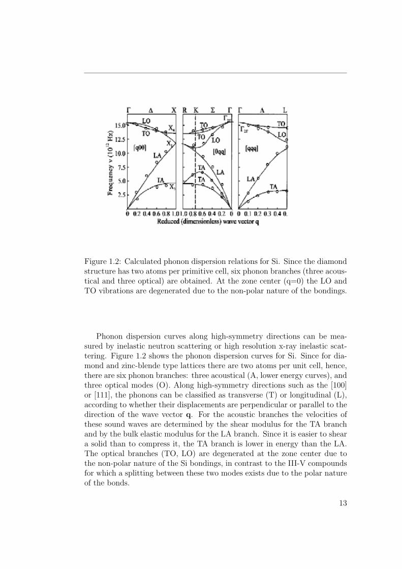
Figure 1.2: Calculated phonon dispersion relations for Si. Since the diamondstructure has two atoms per primitive cell, six phonon branches (three acous-tical and three optical) are obtained. At the zone center (q=0) the LO andTO vibrations are degenerated due to the non-polar nature of the bondings.
Phonon dispersion curves along high-symmetry directions can be mea-sured by inelastic neutron scattering or high resolution x-ray inelastic scat-tering. Figure 1.2 shows the phonon dispersion curves for Si. Since for dia-mond and zinc-blende type lattices there are two atoms per unit cell, hence,there are six phonon branches: three acoustical (A, lower energy curves), andthree optical modes (O). Along high-symmetry directions such as the [100]or [111], the phonons can be classified as transverse (T) or longitudinal (L),according to whether their displacements are perpendicular or parallel to thedirection of the wave vector q. For the acoustic branches the velocities ofthese sound waves are determined by the shear modulus for the TA branchand by the bulk elastic modulus for the LA branch. Since it is easier to sheara solid than to compress it, the TA branch is lower in energy than the LA.The optical branches (TO, LO) are degenerated at the zone center due tothe non-polar nature of the Si bondings, in contrast to the III-V compoundsfor which a splitting between these two modes exists due to the polar natureof the bonds.
13

Theoretical Background
1.1.3 Electron-Phonon Interaction
Until now we have described separately the motion of the electrons [He, seeEq. (1.2)] and ions (Hion) within the Born-Oppenheimer approximation,but a description of the electron-phonon interaction is still lacking (He−ion).Within the spirit of this approximation we assume that the electrons can fol-low the ions almost instantaneously, so that the electron-phonon interactioncan be expanded as a Taylor series in the ions displacements δRj as:
He−ion(ri, δrj) =∑j
(∂He
∂Rj
)∣∣∣∣Rj0
· δRj (1.6)
Usually the electronic Hamiltonian He is not known. In this work we shallconsider the vibrations in diamond or zinc-blende structures with two atomsper unit cell. As we have discussed before, these vibrations can be groupedin four types: LA, TA, LO, and TO phonons.
Considering the physical properties studied in this work, we will considerelectron-phonon interaction of two types:i) Deformation potential interaction is present in crystals with two ormore atoms per primitive cell, a long-wavelength optical phonon involvesrelative displacements of atoms within the primitive unit cell leading to achange in the electronic energies. We can write this interaction as
He−OP = Dn,k ·u
a0
, (1.7)
where Dn,k is the optical phonon deformation potential for the energy bandindexed by n and k. Since the this interaction does not depend on the phononwavevector it is a short range interaction: the Fourier transform of a functionof long range in q is of short range in r and vice versa.
ii) The Frohlich interaction develops in polar crystals with at least twoatoms per primitive cell. The LO phonon induces an oscillating macroscopicpolarization, leading to an electric field ELO. This interaction is not presentin Si or Ge since they are not polar, whereas it is mostly responsible for theelectron-phonon coupling in III-V or II-VI semiconductors like GaAs, AlAs,CdSe, ZnSe, etc.
1.2 Interaction between Light and Matter
We have splitted the general Hamiltonian (1.2) into three contributions aris-ing from the electrons, phonons, and from the electron-phonon interaction.
14

By studying these contributions independently, we have described the elec-tronic excitation spectra, the phonon dispersion curves, and the differenttypes of electron-phonon interaction. In this section, the interaction betweenlight and matter will be presented in order to understand the phenomenathat occur when exciting a semiconductor with electromagnetic radiation.The previous derivation starting from the Hamiltonian will not be followedfor the sake of simplicity. Nevertheless, it is worth to mention that if lighthas to be included in the description of Hamiltonian (1.2) we would have tomake two main modifications:
• p→ p− ecA, where p is the momentum operator of each particle, A is
the potential vector of the electromagnetic field, e the electron charge,and c the speed of light. This modification in the momentum is due tothe presence of an electromagnetic field and gives rise to an interactionbetween the e.m. field and the particles.
• We should also add a term of the form eφ to the Hamiltonian, repre-senting the interaction between the charged particles and the electricfield.
The constitutive equations provide a way to describe the interaction be-tween light and matter. In their macroscopic form these equations describethis interaction via the susceptibility:
P = ε0χE, (1.8)
where ε0 is the electrical susceptibility of the vacuum, P is the polarizationof the medium, χ is the susceptibility, and E is the applied electric field.
This equation shows that when light traveling in vacuum finds a regionof space containing matter (i.e. ε 6= ε0), the atoms will react to the incidente.m. field by creating a polarization field via the susceptibility (χ). This willproduce scattering of the incident e.m. field, which can be elastic and/orinelastic. As an example, absorption of light by materials is no other thanan extreme case of light scattering. The most usual scattering processes aredivided into these two groups:
• Elastic scattering: Rayleigh and Mie. The differences between thesetwo is the wavelength involved, being the one by Rayleigh the appro-priate for describing scattering at small wavelengths
• Inelastic scattering: Raman, Brillouin, Compton. Raman and Bril-louin scattering reefers to scattering of light by optical and acousticphonons, respectively. Compton scattering is the scattering of X-Raysby electrons.
15

Theoretical Background
Since we will be mainly concerned with Raman scattering, I will notdescribe the other types of scattering. Consider a medium with susceptibilityχ, and an incident plane electromagnetic wave as:
E(r, t) = Ei(ki, ωi)cos(ki · r − ωit) (1.9)
When an e.m. field is present in the medium this reacts creating a polar-ization field with the same frequency and wavevector of the incident wave.In addition, if the sample is at a finite temperature the vibrations of theatoms (phonons) will produce fluctuations on χ. The resulting response ofthe medium will be given by Eq. (1.8). Taking into account that the atomicdisplacements (Q) are small, we can expand the susceptibility as:
χ(ki, ωi, Q) = χ0(ki, ωi) + (∂χ/∂Q)0Q(r, t) + ..., (1.10)
using Eq. (1.8) and the incident wave in (1.9) we obtain for the polarizationthe following expression:
P (r, t, Q) = P0(r, t) + Pind(r, t, Q), (1.11)
where P0(r, t) is the contribution arising from the response of the mediumwith no phonons present and Pind(r, t, Q) is the contribution of phonons:
P0(r, t) = ε0χ0(ki, ωi) · Ei(ki, ωi)cos(ki · r − ωit) (1.12)
Pind(r, t, Q) = (∂χ/∂Q)0Q(r, t) · Ei(ki, ωi)cos(ki · r − ωit) (1.13)
Finally, assuming that the atomic displacements associated with a phononcan be expressed as planes waves:
Q(r, t) = Q(q, ω0)cos(q · r − ω0t), (1.14)
and introducing this dependence into Eq. (1.13) we rewrite Pind to determineits frequency and wavevector obtaining:
Pind(r, t, Q) =1
2(∂χ/∂Q)0Q(q, ω0)Fi(ki, ωit)
×cos[(ki + q) · r − (ωi + ω0)t] (1.15)
+cos[(ki − q) · r − (ωi − ω0)t]
This induced polarization consists of two sinusoidal waves: a Stokes compo-nent with wavevector kS = ki − q and frequency ωS = ωi − ω0, and an anti-Stokes component with wavevector kS = ki + q and frequency ωS = ωi + ω0.
16

Notice that both frequency and wavevector are conserved in the Raman pro-cess, so that the wavevector of the one phonon Raman process must beapproximately twice the wavevector of the incident light. Considering visiblelight we have 2ki ≈ 105cm−1, which corresponds to about 1/100 of the Bril-louin zone in a typical semiconductor. Hence, one phonon Raman scatteringprobes only the zone center phonons. Notice that we can obtain high-orderprocesses like two-phonon Raman scattering by expanding (1.10) to higherorders.
In order to obtain the scattered intensity we calculate the time-averagedscattered polarization Pind(r, t, Q) in Eq. (1.13). After some calculation wearrive to the following expression:
Is ∝ |ei · < · es| (1.16)
where Is is scattered intensity, ei and es are the incident and scattered polar-ization directions, and < is the Raman tensor. The Raman tensor propertiesare closely related to the symmetry operations of the crystal, which deter-mine the transitions that are allowed or forbidden, i.e., the so-called Ramanselection rules.
Finally, it is worth to present the complete result for the Raman transitionprobability since effects like resonant-Raman scattering are not obtained inthe previous formulation. The complete result to third order in perturbationtheory obtained using Feynman diagrams is as follows:
Pph =
(2π
~
) ∣∣∣∣∣∑n,n′
〈i|HeR|n′〉〈n′|He−ion|n〉〈n|HeR|i〉[~ωi − (En − Ei)][~ωi − ~ω0 − (En′ − Ei)]
∣∣∣∣∣2
× δ[~ωi − ~ω0 − ~ωs], (1.17)
where 〈i| is the initial state, and 〈n|, 〈n′| are intermediate states. HeR isthe Hamiltonian of the electron-radiation interaction, He−ion is the electron-phonon Hamiltonian, Ej is the energy of the 〈j| state. The frequencies ofthe incident and scattered wave and phonon are denoted as ωi, ωs, and ω0,respectively.
Under resonant conditions the contribution from the non-resonant statescan be regarded as constant. Taking only the strongest term in the Feyn-man diagrams we arrive to the following expression for the case of resonantexcitation:
Pph ≈(
2π
~
) ∣∣∣∣〈0|HeR(ωi)|a〉〈a|He−ion|a〉〈a|HeR(ωs)|0〉(Ea − ~ωi)(Ea − ~ωs)
+ C
∣∣∣∣2 (1.18)
17

Theoretical Background
where Ea is the energy of an intermediate state denoted by 〈a|, and C is aconstant arising from the non-resonant states. From this simplification it ispossible to observe two important and limiting cases of enhanced Pph thatcorrespond to Ea = ~ωi and Ea = ~ωs, known as incoming and outgoingresonance, respectively. This happens when the intermediate state energycoincides with a real energy state of the semiconductor plus/minus the energyof the involved phonon.
1.3 Strain Effects in Semiconductors
In this section the effect of strain in the band structure of semiconductorsand, consequently, in their optical properties will be described. In a simplepicture, a stress applied to a solid leads to a displacement of the atoms fromtheir equilibrium positions, i.e. a phonon may be represented by a strainwave throughout the solid. To obtain the shift in the electronic energiesdue to the presence of a strain we will consider the gradient of the atomicdisplacements:
dij =∂(δRi)
∂Rj
, (1.19)
the purely symmetric part of this quantity is known as strain tensor andrepresents the change in the inter-atomic distances when applying a stress tothe crystal. If we decompose this tensor into a symmetric and anti-symmetriccomponents we obtain the following two tensors:
εij =1
2
(∂δRi
∂Rj
+∂δRj
∂Ri
), fij =
1
2
(∂δRi
∂Rj
− ∂δRj
∂Ri
), (1.20)
where eij is the strain tensor and fij is a pure rotation of the crystal. Thestrain tensor represents a deformation of the solid changing, consequently,the electronic energies in contrast to the anti-symmetric part fij that doesnot change the electronic energies, since it represents a pure rotation of thecrystal. For the zinc-blende structure it can be shown using group theorythat the strain tensor εij can be decomposed into the sum of three linearlyindependent matrices which are the basis of every possible deformation:
18

Mhyd =1
3
ε11 + ε22 + ε33 0 00 ε11 + ε22 + ε33 00 0 ε11 + ε22 + ε33
M[100] =
1
3
2ε11 − (ε22 + ε33) 0 00 2ε22 − (ε11 + ε33) 00 0 2ε33 − (ε11 + ε22)
M[111] =
0 ε12 ε13
ε12 0 ε23
ε13 ε23 0
(1.21)
The matrix Mhyd has a nonzero trace and from the definition of the straintensor components in (1.20) it follows that its trace is equal to the relativevolume change ∆V/V associated with a certain strain. The traceless strainmatrices M[001] and M[111] describe a shear of the crystal produced by uniaxialstress along the [001] and [111] directions, respectively. As a consequence,three deformation potentials are required to describe the effects of a generalstrain on a band extremum.
For the description of the effect of strain on the electronic propertiesof semiconductors Bardeen and Shockley introduced the concept of the de-formation potentials. These deformation potentials were introduced in thecontext of the electron-phonon coupling between long-wavelength (q = 0)acoustic phonons and the valence electrons but their definition has generalvalidity. A pure hydrostatic strain which is applied, for example in high pres-sure experiments with a diamond anvil cell, shifts the electronic states butdoes not split them. The linear components of these shifts are representedby the volume deformation potential ai in (eV ) defined as:
ai =dEi
d(lnV )=
∆Eitr(ε)
, (1.22)
where Ei denotes the energy of state i and V the volume of the crystal.Instead of the hydrostatic deformation potential one often finds in the liter-ature the corresponding pressure coefficient dEi/dP which is related to thedeformation potential through the bulk modulus B:
ai = B · dEidP
(1.23)
Absolute values for ai are difficult to obtain experimentally, as usuallyonly the pressure dependence of gaps are measured, which yields only therelative deformation potential between the bands. Typically, the pressure
19

Theoretical Background
coefficient of the direct band gap at the Γ point of III-V compounds is of theorder of +100 meV/GPa. For the indirect band gap Γ − X it is about anorder of magnitude smaller and negative in sign (-10 meV/GPa) and for theindirect Γ−L gap it is about +50 meV/GPa. Thus, at some pressure the Xvalley become the lowest conduction band (direct-to-indirect crossover), forexample, in bulk GaAs this crossing occurs around 4 GPa.
In contrast to the hydrostatic case, when a uniaxial strain is applied to acrystal (or sub-crystal as 2D layer) its symmetry is reduced. In some casesthis leads to a splitting of degenerated states. Pikus and Bir have derived theHamiltonian within the k · p framework for a general strain. In the absenceof spin-orbit coupling this Hamiltonian is written as:
HPB =a(exx + eyy + ezz) + 3b[(L2x − L2/3)exx + c.p.] (1.24)
+6d√
3
(1
2(LxLy + LyLx)exy + c.p.
),
where a, b, and d are the three Pikus-Bir deformation potentials correspond-ing to strain tensors with symmetries Γ1, Γ3, and Γ4, respectively, c.p. standsfor cyclic permutation and Lj are the angular momentum operators. The de-formation potentials b and d are associated with splittings in the [100] and[111] directions, whereas a is associated with an hydrostatic deformation ofthe crystal.
20

1.4 Effect of Quantum Confinement on Elec-
trons
The effect of quantum confinement on electrons became important in thesemiconductor area after the development of sophisticated growth techniquessuch as molecular beam epitaxy (MBE) and metal-organic chemical vapordeposition (MOCVD), since they allow to grow low-dimensional structures.The confinement effect should be taken into account when any dimension ofa system is comparable to the particle or quasi-particle wavelength, definedby de Broglie as:
λ =h
p=
h
mv
√1− v2
c2, (1.25)
where h is Planck’s constant, m is the particle rest mass, v is the parti-cle velocity, and c is the speed of light in vacuum. Typical examples ofstructures showing quantum confinement are two-dimensional structures re-ferred as quantum wells (QWs), one-dimensional as nanowires, and zero-dimensional as quantum dots (QDs). An important discovery in this fieldwas the quantum Hall effect (QHE) in a two dimensional electron gas,discovered by Klauss Von Klitzing in 1980 for which he was awarded theNobel Prize in 1985.
A typical and very useful example of confinement is given by a particlewith effective mass m∗ confined in a one-dimensional system by infinite po-tential barriers in the z direction. The allowed wavevectors and energy ofthe Bloch wave functions are given by:
kzn =2π
λn= nπ/L, (1.26)
En =~2kzn
2
2m∗=
~2
2m∗n2π2
L2, (1.27)
where n = 1, 2, 3, ... are the indexes of each energy level and L is the thicknessof the potential well (see Fig. 1.3). Thinking of a real quantum well sample,in general the thickness L is subjected to fluctuations due to intrinsic inac-curacies of the growth mechanism, leading to the inhomogeneous broadeningof the confined levels (see Fig. 1.3). The energy dispersion δE as a functionof the potential well thickness fluctuations δL can be calculated from Eq.(1.27) as:
21

Theoretical Background
V
n=0
n=1
n=2
n=3
z
E
L
Figure 1.3: Scheme of a one-dimensional potential well with a barrier V . Fourlevels are shown denoted as n=0,1,2,3. The horizontal band around each levelcorresponds to changes in the energy of each level due to fluctuations in thethickness (L) of the potential well.
δE =~2n2π2
m∗L3δL =
2EnL
δL (1.28)
This result shows that this broadening increases quadratically with thelevel number. In adittion, if we consider a fixed value for the level numbern this broadening increases as the well thickness decreases. This is a purelyquantum effect and should not be confused with the inhomogeneous broad-ening observed, for example, in a distribution of QDs (or QWs) of differentsize.
22

Bibliography
For a complete reference of the Theoretical Background presented in thischapter the reader should reefer to the following sources:
• ”Fundamentals of Semiconductors”, Peter Y. Yu and Manuel Cardona,Springer.
• ”High Pressures in Semiconductors Physics II Vol. 55”, Editors: TadeuszSuski and William Paul, Academic Press.
• ”The Classical Theory of Fileds”, L.D. Landau and E.M. Lifshitz, But-terworth Heinmann.
• ”Quantum Mechanics (Non-Relativistic Theory)”, L.D. Landau andE.M. Lifshitz, Butterworth Heinmann.
23

24

Chapter 2
Experimental Techniques
2.1 Pressure Techniques
One of the pioneers in high pressure physics was P. W. Bridgman who wasawarded the Nobel prize in 1946 for introducing the concept of anvil cell,widely used nowadays. Hydrostatic pressure is created through the deforma-tion of some sealing material with a hole in it serving as pressure chamber,and which is placed between two pistons. Bridgman used tungsten carbidewhich is very hard but opaque and, thus, does not allow for optical mea-surements. The introduction of diamonds as anvils [1] was an importantmilestone on the way to perform optical experiments under high hydrostaticpressure.
2.1.1 Diamond Anvil Cell
The diamond anvil cell (DAC) is a device particularly suited to performoptical measurements under high hydrostatic pressure. The chamber volumewhere the sample is placed is defined inside a 200-300 µm hole drilled into ametal gasket which is closed from the top and bottom by the flat parallel facesof two diamond anvils (see fig.2.1). The sample is subjected to pressure whenthe two diamonds are pushed together decreasing the chamber volume, whileslightly deforming the gasket. Depending on the pressure range and samplevolume, different cells have been built and most of them comprise a movablepiston which holds one of the diamonds and some kind of lever mechanism toapply the pressing force. The cell used in the experiments presented here (fig.2.1) was designed by Syassen and Holzapfel [2] and allows for measurementsup to 25 GPa. Due to the large aperture angle of 36, it is also suitable forRaman experiments.
25

Experimental Techniques
Figure 2.1: Sketch of the diamond anvil cell. Left: Lever mechanism to movethe upper piston. The end points of the levers are driven by two threads.When using the cell in a cryostat two long rods connect the threads with agear outside the cryostat. Right: Illustration of the two diamonds and thegasket.
The gasket is made of a nickel-chromium alloy referred to as InconelX-7501, which is chosen for its mechanical strength and hardness. The fab-rication process of the raw gaskets (small discs of 8 mm in diameter and 250µm in thickness) induces strain in the material, which has to be released toregain its natural hardness. Therefore, they have to run through a temperingprocedure. The discs are then pressed with the diamonds creating a facetedindentation of about 100 µm thickness and 500 µm diameter. This coldforming step represents an additional hardening. Finally, a hole of 200-300µm in diameter is drilled into its center. This hole is the actual sample cham-ber which will be loaded with a sample whose dimensions must not exceed100x100x50 µm3 and a small ruby ball for the pressure determination.
Various organic liquids and condensed gases have been used as pressuremedium to assure hydrostatic conditions in the sample chamber. 4He is oftenchosen for low temperature measurements due to its nearly hydrostatic be-havior up to 60 GPa. In addition, its superfluid phase below 2.2 K simplifiesthe filling up of the cell. For room temperature applications a 4:1 mixtureof methanol and ethanol is used. This mixture can be used only up to ≈13GPa, since at this pressure it solidifies becoming a non-hydrostatic medium.A review of common high pressure techniques can be found in Ref. [3].
2.1.2 Pressure Determination
The pressure in the anvil cell is determined in situ via the pressure dependentshift of the ruby fluorescence. For that purpose a small ruby ball is placedtogether with the sample inside the pressure chamber. The ruby is Cr3+
26

690 692 694 696 698 700
6.3 GPa
3.9 GPa
Intensity (arb. units)
Wavelength (nm)
R1R2 2.3 GPa
Ruby (Al2O3- Cr
3+)
Figure 2.2: Typical Ruby spectra under three different pressures. The twolines R1 and R2 arising for the Cr3+ impurities are shown. The R1 line isthe one used for pressure determination at all temperatures.
doped Al2O3 (Sapphire) and shows a well known strong red fluorescence. Thecrystal symmetry of ruby is rhombohedral, so that the Cr3+ ions and theirsix nearest neighbors form a distorted octahedron whose symmetry is C3 [4].The resulting crystal field leads to a splitting of the degenerated energy levelsof the 3d electrons of Cr3+ giving rise to the two strong fluorescent transitionsdenoted R1 and R2 with energies E(R1) = 14418 cm−1 and E(R2) = 14447cm−1. Applying external pressure decreases the inter-atomic distances and,therefore, the crystal field increases. The level splitting increases resultingin a net reduction of the R1 and R2 transitions energies. The dependence ofthe ruby fluorescence on hydrostatic pressure has been determined up to 80GPa [5]:
P =A
B
[1 +
(λ− λ0
λ0
)]B− 1
, (2.1)
where A = 1904 GPa, B = 7.665, λ0 and λ are the wavelengths of the R1at ambient and given pressure, respectively. As small balls of ruby mightbe strained internally the values for λ0 may differ for each ball representingan error source for the pressure determination. In Fig. 2.2 we show typical
27
Experimental Techniques
spectra of ruby fluorescence at several pressures inside the DAC and withmethanol-ethanol as pressure medium.
For a precise determination of the pressure the dependence of the R1luminescence on temperature has to been taken into account. The pressurecoefficients A and B are independent of temperature to a good approximation[6, 7], whereas the energy of the R1 and R2 lines shifts with temperature.At low temperatures only the low energy R1 line is visible. The temperaturedependence of the R1 line is best described by a two-phonon Raman-processmodel [8], which yields:
νR(T )− νR(0) = α
(T
Θ
)4 ∫ Θ/T
0
x3
ex − 1dx, (2.2)
where ν(T ) is the energy of the R1 band at temperature T and ambientpressure and ν(0) that at 0K. The parameters Θ and α have been determinedby fitting Eq. (2.2) to a comprehensive set of experimental data (Θ = 760 Kand α = 419 cm−1 [9]).
In some of the experiments where samples grown on a Si(100) substratewere investigated, the zone center optical phonon of the substrate was usedfor pressure calibration. The fact that this phonon is intense makes it suitablefor a good pressure determination. As a consequence, loading the ruby ballsinto the cell is avoided, making the procedure easier. The pressure calibrationfor this phonon was done using the previous ruby calibration as:
P = 41.13−√
1691.6 + 16.1× (520.7− ωSi) (2.3)
where P is the pressure in GPa, and ωSi is the frequency of the Si phonon incm−1.
2.1.3 Low Temperature Pressure Technique
When using the DAC at low temperatures with 4He as pressure medium,the loading of the cell is more difficult since it cannot be sealed outside thecryostat. Thus, the DAC has to be loaded with the sample and a rubychip but the diamonds must not close the sample chamber completely. Thecell is placed into the cryostat and is immersed in fluid 4He which will bepumped (with mechanical pump) to lower its equilibrium temperature tillthe transition to the superfluid state at 2.2 K occurs. Under this conditionthe superfluid 4He easily enters into the cell, filling it completely. Finally, theDAC can be sealed by carefully approaching the diamonds. As 4He instantlycrystallizes when subjected to pressure at 2 K the cell has to be heated well
28

above the melting point to relax non-hydrostatic strain. When cooling downagain into the solid phase it is assumed that the pressure on the sample ismostly hydrostatic. The same procedure applies if the pressure is about tobe changed. It is crucial to reach a point in the phase diagram well abovethe melting line such that 4He is liquid during the pressure change.
2.2 Raman Spectroscopy
690 692 694 696 698 700
3000
4000
5000
6000
Inte
nsity
(co
unts
/s)
Wavelength (nm)
Laser
Interferencefilter
Density filter
Mirror
Mirror
Edge filter - 1
Objetive
Sample
Mirror
Edge filter - 2
SlitHole
Grating
CCDSpectrum
Figure 2.3: Schematic diagram of the LabRam HR 800 spectrometer. Twoholographic edge filters are used to filter the laser light.
Although the inelastic scattering of light was predicted by Smekal in 1923,it was not until 1928 that it was observed in practice. The Raman effect wasnamed after one of its discoverers, the Indian scientist Sir C. V. Raman whoobserved the effect by means of sunlight (1928, together with K. S. Krishnanand independently by Grigory Landsberg and Leonid Mandelstam). Ramanwon the Nobel Prize in Physics in 1930 for this discovery accomplished usingsunlight, a narrow band photographic filter to create monochromatic lightand a “crossed” filter to block this monochromatic light. He found that lightof changed frequency passed through the “crossed” filter. Subsequently the
29

Experimental Techniques
mercury arc lamp became the principal light source, first with photographicdetection and then with spectrophotometric detection. Currently lasers areused as light sources.
In this work, Raman spectra were collected using a commercial spectrom-eter optimized for this purpose. One of the most important experimentalcomplications of this technique is that the energy of the Raman excitations(phonons) is of the order of tens of meV, which means that for studyingthis effect we need a device that can filter the incident laser but with a verynarrow bandwidth. This can be achieved in two different ways: i) Filteringthe incident laser with successive gratings, ii) Using an holographic notch oredge filter.
A Jobin Yvon LabRam HR 800 spectrometer based on the edge filtermethod was used for all the experiments. Fig. 2.3 shows a sketch of thespectrometer. The laser filtering procedure is achieved by two successiveedge filters. With this configuration it is possible to measure as close as 50cm−1 from the laser. Another important feature is provided by a confocalmicroscope in order to perform micro-Raman experiments. The confocal ge-ometry which is tuned by changing the aperture of the pinhole (HOLE in Fig.2.3), allows for having spatial resolution in the focus direction. An importantdifference with the grating filtered spectrometer is the loss intensity due to itssuccessive gratings. In the holographic spectrometer only one grating is used,thus, reducing this loss of light in the filtering step. This makes the LabramHR 800 suitable for low signal experiments such as Raman spectroscopy.
30

Bibliography
[1] A. W. Lawson and T.-Y. Tang. A Diamond Bomb for Obtaining PowderPictures at High Pressures. Rev. Sci. Instruments 21, 815 (1975).
[2] K. Syassen and W. B. Holzapfel. In K. D. Timmerhaus and M. S. Barber(editors) Physics of Solids Under High Pressure, volume 1, p. 223 (1979).
[3] A. Jayaraman. Diamond anvil cell and high-pressure physical investiga-tions. Rev. Mod. Phys. 55, 65 (1983).
[4] S. Sugano and Y. Tanabe. Absorption Spectra of Cr3+ in Al2O3. Journalof the Physical Society of Japan 13(8), 880 (1958).
[5] H. K. Mao, J. Xu and P. M. Bell. Calibration of the ruby pressure gaugequasi-hydrostatic conditions. J. Geophys. Res 91, 4673 (1986).
[6] R. A. Noack and W. B. Holzapfel. Calibration of the ruby pressure scaleat low temperatures. In K. D. Timmerhaus and M. S. Barber (editors)High Pressure Science and Technology, p. 748 (Plenum Press, New York,1979, 1979).
[7] G. J. Piermarini and S. Block. Ultrahigh pressure diamond-anvil cell andseveral semiconductor phase transition pressures in relation to the fixedpoint pressure scale. Rev. Sci. Instruments 46, 973 (1975).
[8] D. E. McCumber and M. D. Sturge. Linewidth and Temperature Ruby.Journal of Applied Physics 34(6), 1682 (1963).
[9] J. Yen and M. Nicol. Temperature dependence of the ruby luminescencemeasuring high pressures. Journal of Applied Physics 72(12), 5535 (1992).
31

32

Chapter 3
Results and Discussion
3.1 Phonon Deformation Potentials in strained
SiGe alloys
Although a great amount of work has been done in Si/Ge systems due totheir applications in Si-based technology, some fundamental issues are notproperly addressed to date. Strained SiGe alloys are an example of such dis-appointing state of the art. The complete compositional dependence of theirphonon deformation potentials have not been previously determined. Inthis section, previous results in these fields will be presented in order to pro-vide the reader with a complete view on these topics. Finally, in the lastsubsection, a general conclusion will be given.
3.1.1 Motivation and Previous Work
Strain and Composition determination
The study of the strain status and composition in strained SiGe alloys wassubject of interest since the early 80s. After the first high quality strainedSi1−xGex alloys were grown [1], Cerdeira et. al. [2] studied the zone centeroptical branches using Raman scattering. In this work, only these phononbranches will be taken into account, which in systems like Si or Ge are degen-erated due to the non-polar nature of the bondings. Fig. 3.1 shows a typicalspectrum of a Si0.35Ge0.65 alloy extracted from Ref. [2] where four dominantpeaks are observed at about 300 cm−1, 400 cm−1, 500 cm−1 and 520 cm−1.These correspond to scattering by optical phonons involving Ge-Ge, Si-Ge,Si-Si and Si-Si (substrate) stretching vibrations, respectively. The originof these peaks is well understood [3], and their dependence with composi-tion was measured by Alonso et. al. [4]. Although disorder could introduce
33

Results and Discussion
Figure 3.1: Raman Spectrum of Si1−xGex for x=0.65: a) Single incommen-surate layer and b) Strained superlattice. Extracted from Ref. [2]
alterations, the selection rules for Raman scattering in compositionally disor-dered c-Si1−xGex alloys are the same as for pure c-Si or c-Ge [4]. The strainand composition dependence of the phonon frequency in a pseudomorphicSi1−xGex/Si alloy can be written as:
δω = ω(x, εij)− ω0(x) = ω0(−K11 · α/2 + K12)ε‖, (3.1)
where ω0 is the frequency for zero strain, ε‖ is the in-plane strain, α=2C12/C11
with Cij the elastic constants, and Kij are the phonon deformation potentials(PDPs) as defined by Anastassakis and Cardona[5]. Since no values for thePDPs of the alloys were available, interpolations between the values for pureSi and Ge were used for intermediate concentrations.
From Eq. (3.1) it follows that to determine the strain status of SiGealloys we should first know the values of ω0, K11 and K12. Alonso andWiner grew a series of unstrained alloys in the whole compositional rangeand measured the phonon frequency at zero strain (ω0) for the Ge-Ge, Si-Ge and Si-Si vibrational modes. Their results can be summarized in thefollowing equations, where x is the Ge content:
34

Figure 3.2: Strain shift coefficient for Si1−xGex alloys as a function of Ge con-centration. The solid and opened squares are values for the Si-Si mode. Solidand opened circles are values for the Ge-Ge and Si-Ge modes, respectively.Extracted from Ref. [6].
ωGe−Ge0 = 284 + 5 · x+ 12 · x2 (3.2)
ωSi−Ge0 = 400 + 29 · x− 95 · x2 + 213 · x3 − 170 · x4 (3.3)
ωSi−Si0 = 520− 68 · x (3.4)
No experimental values of the PDPs were known at that moment sincean independent determination of both presents some difficulties. The mostdirect experimental technique would be to perform uniaxial stress measure-ments from where the PDPs are directly extracted, but this approach isproblematic since bulk SiGe alloys of any composition are not easy to grow.An alternative approach by Cerdeira that was used for several years to dealwith the Raman spectra of strained layers was to define the phonon strainshift coefficient following Eq. (3.1). Thus, we can rewrite this equation ina more simple form as δω = bs · ∆ε, where bs is defined as the strain shiftcoefficient, being a linear combination of the PDPs.
35

Results and Discussion
Figure 3.3: Strain shift coefficients for the three Raman modes as a functionof Ge molar fraction x. Solid lines are the results of the calculations, openedand closed symbols are measurements from Refs.[8, 9, 10]. Extracted fromRef. [7].
Subsequent work was focused mainly to obtain bs for the intermediatecompositional range. Lockwood et. al. [6] followed Cerdeira’s approach withsamples between 0 and 0.5 in Ge content. Fig. 3.2 shows their experimentalresults obtained for the strain shift coefficient of the Ge-Ge, Si-Ge and Si-Simodes. The absolute value of the obtained coefficients is rather large, espe-cially in the middle of the composition range. Nevertheless, the used layerswere very thick, well beyond the critical thickness, so that an overestimationof bs is possible if the samples were partially relaxed, which is very likely.For the high Ge content range Stoehr et. al. reported results complementingthe work of Lockwood et. al. Few experimental data were available in thisrange since as the Ge content increases the strain of the epilayer increasesproducing dislocations and, consequently, relaxation of the epilayer. This isthe main reason why experimental data of bs for the whole compositionalrange were lacking in the literature.
Recently Pezzoli et. al. [7] presented calculations of bs for the wholecompositional range using a modified Keating model. Fig. 3.3 shows their
36

results together with values from the literature. This figure summarizes allthe available data to that moment. A great dispersion between the bs valueswith almost no agreement between experiment and theory leads to a baddetermination of the strain status of SiGe alloys.
This problem was solved growing a series of samples by MBE in thewhole compositional range and measuring directly the PDPs by combiningRaman spectroscopy from the cleaved edge with high pressure measurements[see Eqs. (3.5)]. The grown samples were strained Si1−xGex/Si(001) layers.The uniaxial component of the applied strain reduces the crystal symmetryleading to a splitting of optical branches into a doublet (in-plane directions)and a singlet (growth direction). Thus, the singlet to doublet splitting wasmeasured using Raman scattering from the growth direction and cleavededge of the samples. Although these measurements should be enough for anindependent determination of K11 and K12, ω0 is still lacking. It was foundthat for a good determination of the PDPs is crucial to have an accuratevalue of this quantity. In the present approach ω0 is no longer necessarysince the determination of the pressure coefficient of the singlet introducesan additional equation independent of ω0, which, by combining the singletand doublet equations, allows to avoid the ω0 dependence. The equations forthe singlet, doublet, and singlet pressure dependence are written as:
Ωs − ω0 =ω0ε‖C11
[C11K12 − C12K11]
Ωd − ω0 =ω0ε‖2C11
[C11(K11 + K12)− 2C12K12] (3.5)
d(lnΩs)
dP=
1
6BSiGe0
(K11 + 2K12) +1
3
(1
BSiGe0
− 1
BGe0
)(K12 − K11 ·
α
2)
where Bx0 is the bulk modulus and all the other quantities were previously
defined.As was already mentioned, it is possible to combine the first two equations
in (3.5) to obtain a system independent of ω0. Consequently, to determine
K11 and K12 we have to measure Ωs, Ωd, and d(lnΩs)dP
. Finally, the phononstrain shift coefficients are easily calculated using Eq. (3.1)
In the next section the article entitled ”Composition dependence of thephonon strain shift coefficients in SiGe alloys revisited” is presented. Thecompositional dependence for both PDPs and phonon strain shift coefficientfor the three vibrational modes is experimentally determined for the firsttime.
37

Results and Discussion
Figure 3.4: The Gruneisen parameters for Ge-Ge, Si-Ge and Si-Si modes asa function of the Si content x. Extracted from Ref. [12]
Gruneisen Parameter
A confusing literature is also found concerning the Gruneisen parameter forzone center optical phonons in SiGe alloys. This parameter is usually definedas:
γν =B0
ων0
(dων
dP
)= −1
6(K11 + K12), (3.6)
where B0 is the bulk modulus of the material, ων0 is the zero-strain frequency,dων/dP is the pressure derivative of the phonon frequency, and ν refers toa vibrational mode. Renucci et. al. [11] have measured first this parameterin bulk Si0.54Ge0.56 alloys. They obtained the phonon pressure coefficientand computed the Gruneisen parameter, which resulted in 30% bigger valuesthan for pure Ge (γGe ≈ 1). The main contribution to this subject wasmade by Sui et. al. [12]. They have grown polycrystalline SiGe samplescovering almost all the compositional range. Their results for the Gruneisenparameter are shown in Fig. 3.4. Similarly to Renucci et. al., they havefound an increase of this parameter for intermediate Ge contents.
38

As was already mentioned, a precise determination of the phonon pressurecoefficient of the singlet component is necessary to obtain K11 and K12.Once these potentials are determined its easy to compute the Gruneisenparameter using Eq. (3.6). For this purpose another set of samples in thewhole compositional range was grown. A completely different result to thatby Sui et. al. came out. From our measurements the Gruneisen parameterwas found to be approximately independent on composition. These resultsare presented in the next subsection under the title ”Measurement of phononpressure coefficients for a precise determination of deformation potentials inSiGe alloys”. The importance of this contribution can be summarized asfollows: i) They correct all the previous determinations by Renucci and Sui,ii) They are the key to accurately determine the PDPs (K11, K12).
39

3.1.2 Experiments and Results
Article n: 1
Title: Composition dependence of the phonon strain shift coef-ficients in SiGe alloys revisited
Authors: J. S. Reparaz, A. Bernardi, A. R. Goni, M. I. Alonso,and M. Garriga.
Journal: Applied Physics Letters
Article n: 2
Title: Measurement of phonon pressure coefficients for a precisedetermination of deformation potentials in SiGe alloys
Authors: J. S. Reparaz, A. Bernardi, A. R. Goni, M. I. Alonso,and M. Garriga.
Journal: Physica Status Solidi b
41


Composition dependence of the phonon strain shift coefficients of SiGealloys revisited
J. S. Reparaz,a A. Bernardi, A. R. Goñi, M. I. Alonso, and M. GarrigaInstitut de Ciència de Materials de Barcelona-CSIC, Esfera UAB, 08193 Bellaterra, Spain
Received 21 November 2007; accepted 31 January 2008; published online 26 February 2008
By combining Raman scattering from the cleaved edge and under hydrostatic pressure, we haveaccurately determined the tetragonal phonon deformation potentials of strained Si1−xGex alloys inthe entire compositional range for the Ge-like, Si-like, and mixed Si–Ge optical modes. A knownbiaxial strain is induced on thin alloy layers by pseudomorphic epitaxial growth on silicon andsubsequent capping. We also determine the strain shift coefficient of the three modes, which areessentially independent of Ge content between 0.4 and 1. This is key information for an effective useof Raman scattering as strain-characterization tool in SiGe nanostructures. © 2008 AmericanInstitute of Physics. DOI: 10.1063/1.2884526
A precise knowledge of the phonon deformation poten-tials DPs, i.e., the derivative of the optical phonon fre-quency with respect to an elastic deformation of the lattice, iscrucial for an effective use of Raman scattering as powerfulstrain-characterization tool in compound semiconductormicrostructures.1 In particular, for the SiGe material system,there is a great deal of discrepancy between different litera-ture sources about the exact values of the DPs mainly forintermediate Ge concentrations.2–7 There might be many rea-sons for such differences up to a factor of 2 such as strainrelaxation effects for epitaxial layers exceeding the criticalthickness,3 the use of polycrystalline samples,4 or, as pointedout in Ref. 5, due to large uncertainties in the determinationof the phonon frequency for the unstrained alloy as com-pared with literature data obtained for bulk materials.8,9 Suchdisappointing state-of-the-art is surprising in view of thetechnological importance of strained SiGe /Si heterostruc-tures and the great potential of Raman scattering to measurebuilt-in strain in nanostructured materials such assuperlattices,2 self-assembled quantum dots,10–13 andcomplementary metal-oxide semiconductor devices.14
In practice, for the spectroscopical determination ofstrain one needs to know the so-called strain shift coefficient,defined as the ratio of the phonon frequency shift over thestrain that induces the shift: bs= /. For the most fre-quent case of Raman measurements in backscattering geom-etry from the 001 surface, the strain is directly determinedfrom the frequency shift of the Raman-allowed singlet com-ponent of the optical phonons using the expression for thestrain shift coefficient given by2,6
bs = 0− K11 · /2 + K12 . 1
Here, 0 is the frequency of the unstrained phonon mode, Kijare the dimensionless phonon deformation potentials, as de-fined in Ref. 1, and =− represents the relation betweenthe strain in growth direction and in-plane strain. For thecase of a strictly bisotropic stress like in epitaxially grownpseudomorphic layers holds =2C12 /C11, where Cij are theelastic constants of the material. A confusing situation isfound in the literature for the accepted values of the strainshift coefficient of the optical phonons in Si1−xGex alloys:2–7
For intermediate Ge concentrations in the range of 0.3x0.8, the values of bs for the Ge–Ge and the Si–Si mode aretwice as large and about 50% higher than for the pure mate-rials, respectively. This is not only counterintuitive but re-cently appeared theoretical evidence15 for bs being fairlyconstant over the whole concentration range, holding this forthe three optical modes of the SiGe alloy.
In order to clarify this inconsistency, we have grown aset of five strained epitaxial SiGe layers on Si with Ge con-centrations between 0.1 and 0.75 and measured the shift andsplitting of the optical phonons caused by the strain due tothe lattice mismatch between alloy and substrate. From thesemeasurements and that of the pressure coefficient of the sin-glet, we were able to accurately determine two phonon de-
formation potential constants, K11 and K12, as a function ofalloy composition. We obtained for the strain shift coefficientof the Ge–Ge, Si–Ge, and Si–Si alloy modes the same flatdependence on Ge content from pure Ge down to x0.4,followed by a slight increase for lower concentrations. Ourresults are in good qualitative agreement with the calcula-tions of Ref. 15, based on a modified Keating model.
A series of samples containing a strained Si1−xGex alloylayer was grown by molecular beam epitaxy on Si001 sub-strates at a temperature of 400 °C.16 The growth sequenceconsists of deposition of a 100-nm-thick Si buffer layer, fol-lowed by the SiGe alloy layer with thickness below criticalto ensure pseudomorphism and, finally, a 300 nm-thick Sicap layer. A thick cap layer is crucial to avoid elastic strainrelaxation of the SiGe layer after cleavage for micro-Ramanmeasurements from the cleaved edge. The nominal thick-nesses of the alloy layers with a Ge concentration x=0.73,0.55, 0.38, and 0.26 were 7, 10, 7, and 15 nm, respectively.For these layer thicknesses, we estimate an upper bound of0.2 cm−1 for the frequency shift due to phonon-confinementeffects,17 which is negligible compared to other errorsources. For the lowest Ge content of 0.10, a multilayerSiGe /Si structure with a total alloy thickness of 200 nm wasdeposited to increase the Raman signal without exceedingthe critical thickness. The strain and composition of the al-loys were determined by x-ray reciprocal space mappingalong the 224 diffraction direction and for the lattice con-stant dependence on composition, we used the relation givenelsewhere.18,19 All alloys showed good pseudomorphicgrowth to Si.aElectronic mail: [email protected].
APPLIED PHYSICS LETTERS 92, 081909 2008
0003-6951/2008/928/081909/3/$23.00 © 2008 American Institute of Physics92, 081909-1Downloaded 08 Jul 2008 to 158.109.18.63. Redistribution subject to AIP license or copyright; see http://apl.aip.org/apl/copyright.jsp

Raman spectra were collected in backscattering geom-etry at room temperature using the 514.5 nm line of an Ar+
laser. Raman peak positions are determined with an error ofless than 0.5 cm−1. Special care was taken to keep laserpower as low as possible to avoid laser heating and the con-sequent but spurious redshift of the Raman peaks, mainlywhen exciting at the cleaved edge. A laser power density of1.5 kW /cm2 turned out to be adequate. Measurements underpressure were carried out using the diamond anvil cellDAC technique. A 4:1 mixture of methanol and ethanolwas employed as the pressure-transmitting medium. Pressurewas monitored in situ by the shift of the Si longitudinaloptical phonon. Samples with similar alloy composition butwithout cap layer were grown for the Raman experimentsunder pressure. Samples loaded into the DAC were previ-ously thinned to about 30 m by mechanical polishing.
The threefold degeneracy of the optical phonon modes atthe Brillouin-zone center is lifted at the alloy layer due to thetetragonal distortion of the lattice caused by the bisotropicstress induced by its lattice mismatch to Si. The zone-centerphonons split into a singlet s, vibrations in growth directionand a doublet d, in-plane vibrations component which areapparent in Raman spectra with different linearly polarizedlight configurations owing to the following selection rules:the singlet component is observed in backscattering from thegrowth direction using the geometry zxyz, whereas, thedoublet component appears in spectra measured in back-scattering from the cleaved edge xzyx, where x, y, z, x,
and y are the 100, 010, 001, 110, and 110 crystal-lographic directions, respectively. Figure 1 shows two repre-sentative spectra of the alloy with 0.55 Ge content. Geom-etries with crossed linear polarization were chosen onpurpose in order to suppress contributions from second-orderRaman processes by acoustic phonons in Si, which wouldhave hampered the precise determination of the peak posi-tion mainly for the Ge–Ge mode. The position of all Raman
peaks was determined by a conventional least-squares fittingprocedure using asymmetric Gaussians for the alloy modesand a Lorentzian for the Raman peak of the Si layers. Thefrequency splitting between peaks measured using both scat-tering geometries is indicative of a tetragonal strain in thealloy layer. Splitting values of the three alloy modes are plot-ted as a function of alloy composition in the inset of Fig. 1.The Ge–Ge mode splitting increases linearly with Ge con-centration, whereas, for the other modes, the increase of thesplitting is sublinear.
The hydrostatic strain-induced shift of the phonon fre-quencies and the singlet-doublet splitting, which are linearon the strain = aSi−a0x /a0x given by the lattice mis-match, can be written in terms of the adimensional phonondeformation potentials as1,20
s + 2d
30= 1 +
2 −
6K11 + 2K12 , 2
s − d
0= −
1 +
2K11 − K12 . 3
Using these equations, one should be able to determine thephonon DPs of the alloys from the measured frequencies ofthe singlet and doublet components. This method, however,presents a major drawback which concerns large uncertain-ties derived from the estimation of the unstrained frequency0 from literature data.5,8 As an alternative, we propose toget rid of 0 by division of Eq. 2 by Eq. 3, adding a thirdequation which corresponds to the hydrostatic pressure coef-ficient of the singlet frequency. For that purpose, we haveperformed Raman measurements using the DAC for everyconcentration. The logarithmic derivative of the phonon fre-quency over pressure is readily calculated as:13
6d ln s
dP= −
K11 + 2K12
B0SiGe + 2K12 − K11 1
B0SiGe −
1
B0Si , 4
where B0 is the bulk modulus of the corresponding material.For the alloys, B0 was obtained by linear interpolation be-tween the values of the pure elements. The second term inEq. 4 represents the correction to the phonon pressure co-efficient due to the different elastic properties of alloy and Sisubstrate, which tends to reduce the lattice mismatch strainwith increasing pressure. This correction amounts up to 15%for high Ge concentrations, hence, it has to be taken intoaccount for an accurate determination of the phonon DPs.The key point is that 0 does not appear explicitly in Eq. 4.
We obtain a system of two linear equations with twounknowns, which is easily solved to obtain the phonon de-
formation potentials K11 and K12 plotted in Fig. 2 as a func-tion of Ge concentration for the three optical modes of theSiGe alloy. The values corresponding to the pure materialsare the ones tabulated in Ref. 1, but for Ge, they were in-creased in absolute value by 13.5% in order to account for
the correct Grüneisen parameter = K11+2K12 /6 obtainedfrom hydrostatic pressure experiments.21 As already per-formed for GaAs Ref. 22 and Si,23 such a correction isnecessary because of a systematic underestimation of the ap-plied stress due to surface strain relaxation in the uniaxial-stress Raman experiments performed with a laser energyabove the band gap of the material. Despite the relativelylarge error bars for Si rich alloys, the overall picture that
FIG. 1. Representative Raman spectra of a strained alloy layer with Gecontent x=0.55 measured at room temperature in different scattering con-figurations with crossed linearly polarized light. Peak assignment to theoptical modes of the alloy is indicated. Solid lines represent the results ofleast-squares fits to the spectra using asymmetric Gaussians. The insetshows the values of the singlet-doublet splitting for the three optical alloymodes as a function of Ge concentration.
081909-2 Reparaz et al. Appl. Phys. Lett. 92, 081909 2008
Downloaded 08 Jul 2008 to 158.109.18.63. Redistribution subject to AIP license or copyright; see http://apl.aip.org/apl/copyright.jsp
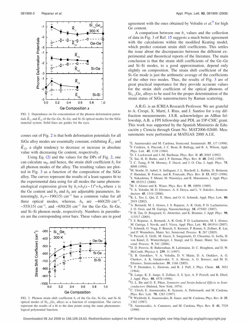
comes out of Fig. 2 is that both deformation potentials for all
SiGe alloy modes are essentially constant, exhibiting K11 and
K12, a slight tendency to decrease or increase in absolutevalue with decreasing Ge content, respectively.
Using Eq. 2 and the values for the DPs of Fig. 2, onecan calculate 0, and hence, the strain shift coefficient bs forall phonon modes of the alloy. The resulting values are plot-ted in Fig. 3 as a function of the composition of the SiGealloy. The curves represent the results of a least-squares fit tothe experimental data using for all modes the same phenom-enological expression given by bs=b4x−14+b0,where x isthe Ge content and b4 and b0 are adjustable parameters. In-terestingly, b4=−19015 cm−1 has a common value for allthree optical modes, whereas, b0 are −46020 cm−1,−55515 cm−1, and −65020 cm−1 for the Ge–Ge, Si–Ge,and Si–Si phonon mode, respectively. Numbers in parenthe-sis are the corresponding error bars. These values are in good
agreement with the ones obtained by Volodin et al.9 for highGe content.
A comparison between our bs values and the collectionof data in Fig. 3 of Ref. 15 suggests a much better agreementwith the calculations within the modified Keating model,which predict constant strain shift coefficients. This settlesthe issue about the discrepancies between the different ex-perimental and theoretical reports of the literature. The mainconclusion is that the strain shift coefficients of the Ge–Geand Si–Si modes, to a good approximation, depend onlyslightly on composition. The strain shift coefficient of theSi–Ge mode is just the arithmetic average of the coefficientsof the other two modes. Thus, the results of Fig. 3 are ofgreat practical importance for they provide accurate valuesfor the strain shift coefficient of the optical phonons ofSi1−xGex alloys to be used for the proper determination of thestrain status of SiGe nanostructures by Raman scattering.
A.R.G. is an ICREA Research Professor. We are gratefulto A. Crespi, X. Martí, J. Rius, and J. Santiso for x-ray dif-fraction measurements. J.S.R. acknowledges an AlBan fel-lowship, A.B. a FPI fellowship and PDL an I3P-CSIC grant.This work was supported by the Spanish Ministerio de Edu-cación y Ciencia through Grant No. MAT2006-02680. Mea-surements were performed at MATGAS 2000 A.I.E.
1E. Anastassakis and M. Cardona, Semicond. Semimetals 55, 117 1998.2F. Cerdeira, A. Pinczuk, J. C. Bean, B. Batlogg, and B. A. Wilson, Appl.Phys. Lett. 45, 1138 1984.
3D. J. Lockwood and J.-M. Baribeau, Phys. Rev. B 45, 8565 1992.4Z. Sui, H. H. Burke, and I. P. Herman, Phys. Rev. B 48, 2162 1993.5J. C. Tsang, P. M. Mooney, F. Dacol, and J. O. Chu, J. Appl. Phys. 75,8098 1994.
6M. Stoehr, D. Aubel, S. Juillaguet, J. L. Bischoff, L. Kubler, D. Bolmont,F. Hamdani, B. Fraisse, and R. Fourcade, Phys. Rev. B 53, 6923 1996.
7S. Nakashima, T. Mitani, M. Ninomiya, and K. Matsumoto, J. Appl. Phys.99, 053512 2006.
8M. I. Alonso and K. Winer, Phys. Rev. B 39, 10056 1989.9V. A. Volodin, M. D. Efremov, A. S. Derya, and L. V. Sokolov, Semicon-ductors 45, 1314 2006.
10K. L. Teo, L. Qin, Z. X. Shen, and O. G. Schmidt, Appl. Phys. Lett. 80,2919 2002.
11A. Bernardi, M. I. Alonso, J. S. Reparaz, A. R. Goñi, P. D. Lacharmoise,J. O. Ossó, and M. Garriga, Nanotechnology 18, 475401 2007.
12P. H. Tan, D. Bougeard, G. Abstreiter, and K. Brunner, J. Appl. Phys. 98,113517 2005.
13J. S. Reparaz, A. Bernardi, A. R. Goñi, P. D. Lacharmoise, M. I. Alonso,M. Garriga, J. Novák, and I. Vávra, Appl. Phys. Lett. 91, 081914 2007.
14J. Schmidt, G. Vogg, F. Bensch, S. Kreuzer, P. Ramm, S. Zollner, R. Liu,and P. Wennekers, Mater. Sci. Semicond. Process. 8, 267 2005.
15F. Pezzoli, E. Grilli, M. Guzzi, S. Sanguinetti, D. Chrastina, G. Isella, H.von Känel, E. Wintersberger, J. Stangl, and G. Bauer, Mater. Sci. Semi-cond. Process. 9, 541 2006.
16D. D. Perovic, B. Bahierathan, H. Lafontaine, D. C. Houghton, and D. W.McComb, Physica A 239, 11 1997.
17E. B. Gorokhov, V. A. Volodin, D. V. Marin, D. A. Orekhov, A. G.Cherkov, A. K. Gutakovskii, V. A. Shvets, A. G. Borisov, and M. D.Efremov, Semiconductors 39, 1168 2005.
18J. P. Dismukes, L. Ekstrom, and R. J. Paff, J. Phys. Chem. 68, 30211964.
19R. Lange, K. E. Junge, S. Zollner, S. S. Iyer, A. P. Powell, and K. Eberl,J. Appl. Phys. 80, 4578 1996.
20G. L. Bir and G. E. Pikus, Symmetry and Strain-Induced Effects in Semi-conductors Halsted, New York, 1974.
21C. Ulrich, E. Anastassakis, K. Syassen, A. Debernardi, and M. Cardona,Phys. Rev. Lett. 78, 1283 1997.
22P. Wickbold, E. Anastassakis, R. Sauer, and M. Cardona, Phys. Rev. B 35,1362 1987.
23E. Anastassakis, A. Cantarero, and M. Cardona, Phys. Rev. B 41, 75291990.
FIG. 2. Dependence on Ge concentration of the phonon deformation poten-
tials K11 and K12 of the Ge–Ge, Si–Ge, and Si–Si optical modes for the SiGematerial system. Solid lines are guides for the eyes.
FIG. 3. Phonon strain shift coefficient bs of the Ge–Ge, Si–Ge, and Si–Sioptical modes of Si1−xGex alloys as a function of composition. The curvesrepresent the results of a fit to the data points using the same phenomeno-logical polynomial function.
081909-3 Reparaz et al. Appl. Phys. Lett. 92, 081909 2008
Downloaded 08 Jul 2008 to 158.109.18.63. Redistribution subject to AIP license or copyright; see http://apl.aip.org/apl/copyright.jsp


physica status solidi, 15 June 2008
Measurement of phonon pressurecoefficients for a precisedetermination of deformationpotentials in SiGe alloys
J. S. Reparaz1, A. R. Goñi1,*, A. Bernardi1, M. I. Alonso1, M. Garriga1
1 Institut de Ciència de Materials de Barcelona-CSIC, Esfera UAB, 08193 Bellaterra, Spain
Received XXXX, revised XXXX, accepted XXXXPublished online XXXX
PACS 63.50.Gh, 78.30.-j, 78.30.Am, 62.50.-p
∗ Corresponding author: e-mail [email protected], Phone +34-93-5801853, Fax +34-93-5805729
For an effective use of Raman scattering as strain char-acterization tool in SiGe nanostructures a precise knowl-edge of the phonon deformation potentials (DPs) isstrictly necessary. The optical phonon DPs can be de-termined by means of Raman scattering measurementsfrom the cleaved edge of a biaxially strained SiGe al-loy layer grown pseudomorphically on silicon and subse-quently capped. Due to uncertainties in the literature val-ues of the unstrained phonon frequencies it turns out thatthe desired degree of accuracy is only attained by com-plementing the Raman measurements from the edge withthat of the hydrostatic pressure coefficient of the opticalphonons. For that purpose we have grown by molecularbeam epitaxy up to seven partially strained Si1−xGex al-loys on Si spanning the entire compositional range andmeasured the dependence on hydrostatic pressure of thefrequency of the Ge-like, Si-like and mixed Si-Ge opticalmodes.
After correcting for the pressure dependent biaxial stressinduced by the Si substrate on the alloy layer and tak-ing into account the dependence on alloy compositionof the bulk modulus we obtain a fairly constant value ofthe Grüneisen parameter around 1.0 for all three opticalmodes in the whole range of Ge contents. We also de-termined the strain shift coefficients for the three modes,which are essentially independent of Ge content between0.4 and 1. Our results are in very good agreement withrecent calculations of the SiGe phonon deformation po-tentials using a modified Keating model, which settlesthe longstanding issue about the large discrepancies be-tween results from different experiments.
Copyright line will be provided by the publisher
1 Introduction Raman scattering has demonstrated tobe a powerful strain-characterization tool in compoundsemiconductor microstructures [1]. The accuracy of sucha determination, though, depends much on the preciseknowledge of the phonon deformation potentials (DPs),i.e., the derivative of the optical phonon frequency withrespect to an elastic deformation of the lattice. In this re-spect, the situation found in the literature for the SiGe ma-terial system is particularly disappointing. There is a greatdeal of discrepancy between different sources about thevalues of the DPs mainly for intermediate Ge concentra-tions [2–7]. As pointed out in Ref. [5] the most probable
reason for such differences arises from the fact that the ac-tual value of the phonon frequency for the unstrained al-loy is obtained from the literature data for bulk materials[8,9] although it appears to be sample dependent. In a re-cent paper [10], however, we demonstrate that it is possibleto circumvent the problem posed by the exact knowledgeof ω0, the unstrained frequency of any particular phononmode, by using its hydrostatic pressure coefficient as anadditional input parameter. In this way, we were able tocomplement information about shifts and splitting of thephonon modes measured from the cleaved edge in samplescontaining strained SiGe alloy layers of different composi-
Copyright line will be provided by the publisher

2 Reparaz et al.: Phonon pressure coefficients of SiGe alloys
tions to obtain a linear system of two equations with twounknowns, which is solved for a precise determination ofthe dimensionless phonon deformation potential constants,K11 and K12, as defined in Ref. [1]. Needless to say thatω0 does not appear explicitly in these equations.
In this work we present the results on the hydrostaticpressure coefficient of the three optical modes of SiGe al-loys in the entire range of compositions used for the pre-cise determination of the DPs reported in Ref. [10]. Forthat purpose we have grown a set of seven thick, partiallystrained epitaxial SiGe layers on Si with Ge concentrationsbetween 0.1 and 1.0 and used the diamond- anvil cell tech-nique to measure the pressure-induced shift of the opticalphonons by Raman scattering. We found that the Grüneisenparameter (the logarithmic derivative of the frequency withrespect to volume) for all three phonon modes is close to1.0, being independent of the Ge content. In this way andusing the results of Ref. [10], we obtained for the Ge-Ge,Si-Ge and Si-Si alloy modes the value of the so-calledstrain shift coefficient, defined as the ratio of the phononfrequency shift over the strain that induces that shift, asa function of alloy composition. Our results are in goodqualitative agreement with recent calculations based on amodified Keating model [11].
2 Experimental A series of samples containing athick, partially relaxed Si1−xGex alloy layer with x=0.19,0.26, 0.39, 0.47, 0.55, 0.74 and 1.00 was grown by molec-ular beam epitaxy on Si(001) substrates at a temperatureof 400 oC. The growth sequence consists of deposition ofa 100 nm-thick Si buffer layer followed by the SiGe al-loy layer with thickness ranging between 100 and 500 nm.Such large values which are in most cases beyond the criti-cal thickness for the given Ge content [12] were necessaryto attain reasonable signal-to-noise ratios for Raman scat-tering inside the pressure cell. Thus, partial or even totalstrain relaxation of the SiGe layers is unavoidable, mainlyfor the higher Ge concentrations. Nevertheless, we pointout that within the linear approximation (constant bulkmodulus independent of pressure) the amount of strain re-laxation is irrelevant for the determination of the pressurecoefficient of the phonon frequency. The same holds forthe correction due to the presence of the Si substrate whichhas a different bulk modulus than the alloy layer grownpseudomorphically on top. Finally, the composition of thealloys was determined by x-ray reciprocal space mappingalong the (224) diffraction direction.
Raman spectra were collected with a LabRam HR800system equipped with a large working distance microscopeobjective in backscattering geometry at room temperatureusing the 514.5 nm line of an Ar+ laser. Raman peak po-sitions are determined with an error of less than 0.5 cm−1.A laser power density of 1.5 kW/cm2 turned out to beadequate to avoid laser heating and the consequent butspurious redshift of the Raman peaks. Measurements un-der pressure were carried out using the diamond anvil cell
250 300 350 400 450 500 550
0 2 4 6
5.70
5.75
3.8 GPa
Ge-Ge
Si-Si
Si-Ge
Inte
nsity
(ar
b. u
nits
)Raman Shift (cm-1)
x=0.47
Ge-Ge
0.9 GPa
ln(ω
s)
P (GPa)
Si1-x
Gex
Figure 1 Two representative Raman spectra of an alloy layer withGe content x=0.47 measured at hydrostatic pressures of 0.9 and3.8 GPa. Peak assignment to the optical modes of the alloy is indi-cated. The inset shows, as an example, the values of the logarithmof the frequency for the Ge-Ge optical alloy mode as a functionof pressure. The straight line represents a least-squares fit throughthe data points.
(DAC) technique. A 4:1 mixture of methanol and ethanolwas employed as the pressure-transmitting medium. Pres-sure was monitored in situ by the shift of the Si longitudi-nal optical phonon, which was previously calibrated usingthe pressure shift of the ruby R1 line [13]. Samples loadedinto the DAC were previously thinned to about 30 µm bymechanical polishing.
3 Results and Discussion The three-fold degener-acy of the optical phonon modes at the Brillouin-zone cen-ter is lifted at the alloy layer due to the tetragonal distortionof the lattice caused by the bisotropic stress induced by itslattice mismatch to Si. The zone-center phonons split intoa singlet (s, vibrations in growth direction) and a doublet(d, in-plane vibrations) component. For the case of Ramanmeasurements in backscattering geometry from the (001)surface the shift of the frequency ωs of the Raman-allowedsinglet component of the optical phonons is linear on thestrain ∆ε = aSi−a0(x)
a0(x) given by the lattice mismatch ac-cording to
ωs = ω0 + bs ·∆ε. (1)
The expression for the strain shift coefficient as a functionof the DPs is given by [2,6]
bs = ω0 · (−K11 · α/2 + K12). (2)
Copyright line will be provided by the publisher

pss header will be provided by the publisher 3
For the case of a strictly bisotropic stress like in epitaxiallygrown pseudomorphic layers holds α = 2C12
C11, where Cij
are the elastic constants of the material.In addition, the frequency shift induced by the external
hydrostatic pressure in the diamond anvil cell can be alsowritten in terms of the phonon deformation potentials as[14,1]
ωs = ω0 ·(
1 +γP
BSiGe0
), (3)
γ = −K11 + 2K12
6, (4)
where γ is the mode Grüneisen parameter. By adding thecontributions from Eqs. (1) and (3) one readily obtains forthe logarithmic derivative of the phonon frequency overpressure following expression [15]
dlnωs
dP=
γ
BSiGe0
+bs
3ω0·(
1BSiGe
0
− 1BSi
0
). (5)
The second term in Eq. (5) represents the correction tothe phonon pressure coefficient due to the different elasticproperties of alloy and Si substrate, which tends to reducethe lattice mismatch strain with increasing pressure. Thiscorrection amounts up to 15% for high Ge concentrations,hence, it has to be taken into account for an accurate deter-mination of the Grüneisen parameters.
Figure 1 shows two representative spectra of the alloywith a Ge content of 0.47 measured at pressures of 0.9and 3.8 GPa. The assignment of the optical modes cor-responding to the Ge-Ge, Si-Ge and one of the Si-Si al-loy vibrations is indicated [8]. To increase the signal-to-noise ratio in the DAC detection is not polarized. Thus, itis not possible to suppress contributions from second-orderRaman processes by acoustic phonons in the Si substrate.This gives rise to the features around 300 and 450 cm−1,which sometimes might interfere with the precise determi-nation of the peak position mainly for the Ge-Ge mode.The position of all Raman peaks was determined by a con-ventional least-squares fitting procedure using asymmet-ric Gaussians for the Ge-Ge and Si-Ge alloy modes anda Lorentzian for the Si-Si ones. All alloy modes shift tohigher frequencies with increasing pressure. As an exam-ple, we plot in the inset to Fig. 1 the logarithm of the Ge-Gemode frequency as a function of pressure. A great advan-tage of this representation is that in the pressure range up to5 GPa ln(ωs) exhibits for all optical modes a totally lineardependence on pressure irrespective of alloy composition.Thus, the slope dlnωs
dP fully characterizes the pressure be-havior of the phonon modes. In contrast, a parabolic depen-dence is very often encountered within the conventionalpractice of plotting frequency against pressure, which leadsto different results for the linear pressure coefficient de-pending on the criteria used to account for the curvature.
Using the slopes determined from linear fits to theln(ωs)-vs.-P data points and the frequency values for zero
0.0 0.2 0.4 0.6 0.8 1.0
5.0
5.5
6.0
6.5
Si-Si P
ress
ure
Coe
ffici
ent (
cm-1/G
Pa)
Ge Composition
4.5
5.0
5.5
6.0
Si-Ge
3.0
3.5
4.0
4.5
Ge-Ge
Si1-x
Gex
Figure 2 (closed symbols) Dependence on Ge concentration ofthe phonon linear pressure coefficient of the Ge-Ge, Si-Ge, andSi-Si optical modes for the SiGe material system. Open circlescorrespond to the values of the pressure coefficient after correc-tion for the effect of the biaxial stress caused by the Si substrate.Solid lines are guides to the eye.
pressure we obtained the linear pressure coefficients of theoptical phonons of the alloys plotted in Fig. 2 (closed sym-bols) as a function of Ge content. The solid curves areguides to the eye. These data were used to complementthe Raman measurements from the cleaved edge of fullystressed alloy layers for the precise determination of thephonon deformation potentials K11 and K12, as previouslyreported in Ref. [10]. With this knowledge of the DPs wemake use of Eq. (5) to calculate the correction to the linearpressure coefficient due to the pressure-induced changesin the biaxial strain caused by the Si substrate. The result-ing coefficients, which are plotted in Fig. 2 as open cir-cles, correspond to the values that would be obtained forthe bulk alloy material, i.e. for free-standing alloy samples.As pointed out before, the higher the Ge concentration, thelarger is the correction due to the significant difference inbulk modulus between alloy and Si substrate. We empha-size that whereas for the Ge-Ge and Si-Ge modes at in-termediate Ge concentrations the pressure coefficients ob-tained in Ref. [4] are about 30% larger than ours, we findvery good agreement with the results of calculations withina modified Keating model [11]. We believe that in the for-
Copyright line will be provided by the publisher

4 Reparaz et al.: Phonon pressure coefficients of SiGe alloys
mer case the discrepancy is likely due to the polycrystallinecharacter of the samples employed in Ref. [4].
The mode Grüneisen parameters γ are thus extractedfrom the corrected values of the linear pressure coefficientsusing Eq. (5). For the alloys the bulk modulus B0 was ob-tained by linear interpolation between the ones of the pureelements [16]. Figure 3 shows the resulting γ values of theoptical phonon modes of the alloys for the whole range ofcompositions. A striking result concerns the fact that theGrüneisen parameters of all three modes are almost con-stant and very similar in absolute value, being its averageequal to 1.00±0.05. This is in frank contrast with severalliterature sources, where γ values as large as 1.3 to 1.4are reported for intermediate Ge concentrations [4,6]. Fur-thermore, a constant γ implies that the observed variationof the phonon pressure coefficient with alloy composition(see Fig. 2) is due only to a change in bulk modulus. Thisis actually very intuitive since the Grüneisen parameters ofthe pure materials differ only by 5%, thus, no appreciabledependence on composition is to be expected.
0.0 0.2 0.4 0.6 0.8 1.0
0.6
0.8
1.0
1.2
1.4 Si1-x
Gex
300 K
Grü
neis
en P
aram
eter
γ
Ge Composition
Ge-Ge Si-Ge Si-Si
Figure 3 Mode Grüneisen parameter γ of the Ge-Ge (full cir-cles), Si-Ge (half-filled circles) and Si-Si (open circles) opticalphonons of Si1−xGex alloys as a function of composition.
Due to its practical importance it is very instructive tocompare our results for the strain shift coefficient bs forall phonon modes of the alloy with the available literaturedata. bs is readily obtained from the values for the DPs ofRef. [10] using Eq. (2). Results are plotted in Fig. 4 (fulldata points) as a function of composition. The dot-dashedcurves represent the results of a least-squares fit to the ex-perimental data using for all modes the same phenomeno-logical expression given by
bs = b4 · (x− 1)4 + b0,
where x is the Ge content and b4, b0 are adjustable param-eters. Interestingly, b4 = −190(15) cm−1 has a common
value for all three optical modes, whereas b0 is −460(20)cm−1, −555(15) cm−1 and −650(20) cm−1 for the Ge-Ge, Si-Ge and Si-Si phonon mode, respectively. Numbersin parentheses are the corresponding error bars.
Until very recently, a confusing situation was found inthe literature for the accepted values of the phonon strainshift coefficients in Si1−xGex alloys [2–7]. As illustratedin Fig. 4, for intermediate Ge concentrations in the range0.3 ≤ x ≤ 0.8 the values of bs are 50 to 100% higher thanfor the pure materials, respectively. This is not only coun-terintuitive but recently appeared theoretical evidence [11]for bs being nearly constant over the whole concentrationrange, holding this for the three optical modes of the SiGealloy. In fact, our data are in fairly good agreement withthese calculations within the modified Keating model. Theagreement is also good with the bs values of the Ge-Gemode obtained by Volodin et al. [9] for high Ge content(solid straight line with small diamonds in Fig. 4).
0.0 0.2 0.4 0.6 0.8 1.0
-1000
-800
-600
Si-Si
Str
ain
Shi
ft C
oeffi
cien
t (cm
-1)
Ge Composition
-900
-700
-500
Si-Ge
Ge-Ge
-1000
-800
-600
-400
Figure 4 Phonon strain shift coefficient bs of the Ge-Ge, Si-Ge and Si-Si optical modes of Si1−xGex alloys as a function ofcomposition. Closed symbols represent our results [10], open cir-cles correspond to the experimental results of Refs. [17,7,18,11]and solid curves are the results of the Keating-model calculations[11]. The solid straight lines with the small diamonds representthe experimental results of Ref. [9].
Copyright line will be provided by the publisher

pss header will be provided by the publisher 5
4 Conclusions The measurements of the linear pres-sure coefficient for the optical phonon modes in the en-tire compositional range of SiGe alloys were crucial forthe precise determination of the corresponding strain shiftcoefficients. In this way, we have settled the issue aboutthe discrepancies between the different experimental andtheoretical values for bs. Hence, these results are of greatpractical relevance for they provide accurate strain shift co-efficients for the optical phonon modes to be used for theproper determination of the strain status of SiGe nanostruc-tures by Raman scattering.
Acknowledgements A.R.G. is an ICREA Research Pro-fessor. We are grateful to A. Crespi, X. Martí, J. Rius and J.Santiso for x-ray diffraction measurements. J.S.R. acknowledgesfinancial support from the AlBan fellowship Program. A.B. ac-knowledges an FPI fellowship. This work was supported in partby the Spanish Ministerio de Educación y Ciencia through grantMAT2006-02680. Measurements were performed at the Nan-otechnology Laboratory of MATGAS 2000 A.I.E.
References
[1] E. Anastassakis and M. Cardona, Semicond. Semimetals 55,117 (1998) and references therein.
[2] F. Cerdeira, A. Pinczuk, J. C. Bean, B. Batlogg, and B. A.Wilson, Appl. Phys. Lett. 45, 1138 (1984).
[3] D. J. Lockwood and J. M. Baribeau, Phys. Rev. B 45, 8565(1992).
[4] Z. Sui, H. H. Burke, and I. P. Herman, Phys. Rev. B 48, 2162(1993).
[5] J. C. Tsang, P. M. Mooney, F. Dacol, and J. O. Chu, J. Appl.Phys. 75, 8098 (1994).
[6] M. Stoehr, D. Aubel, S. Juillaguet, J. L. Bischoff, L. Kubler,D. Bolmont, F. Hamdani, B. Fraisse, and R. Fourcade, Phys.Rev. B 53, 6923 (1996).
[7] S. Nakashima, T. Mitani, M. Ninomiya, and K. Matsumoto,J. Appl. Phys. 99, 053512 (2006).
[8] M. I. Alonso and K. Winer, Phys. Rev. B 39, 10056 (1989).[9] V. A. Volodin, M. D. Efremov, A. S.Derya, and L. V.
Sokolov, Semicond. 45, 1314 (2006).[10] J. S. Reparaz, A. Bernardi, A. R. Goñi, M. I. Alonso, and M.
Garriga, Appl. Phys. Lett. 92, 081909 (2008).[11] F. Pezzoli, E. Grilli, M. Guzzi, S. Sanguinetti, D. Chrastina,
G. Isella, H. von Känel, E. Wintersberger, J. Stangl, and G.Bauer, Mat. Sci. Semicond. Processing 9, 541 (2006).
[12] D. D. Perovic’, B. Bahierathan, H. Lafontaine, D. C.Houghton, and D. W. McComb, Physica A 239, 11 (1997).
[13] H. K. Mao, J. Xu, and P. M. Bell, J. Geophy. Res. 91, 4673(1986).
[14] G. L. Bir and G. E. Pikus, Symmetry and Strain-induced Ef-fects in Semiconductors (Halsted Press, New York, 1974).
[15] J. S. Reparaz, A. Bernardi, A. R. Goñi, P. D. Lacharmoise,M. I. Alonso, M. Garriga, J. Novák, and I. Vávra, Appl.Phys. Lett. 91, 081914 (2007).
[16] Numerical Data and Functional Relationships in Scienceand Technolog, Landolt-Börnstein, New Series Vol. 17,edited by O. Madelung, H. Weiss, and M. Schulz (Springer,Heidelberg, 1982), Sec. 2, p. 64 and 107.
[17] J. Schmidt, G. Vogg, F. Bensch, S. Kreuzer, P. Ramm, S.Zollner, R. Liu, and P. Wennekers, Mat. Sci. Semicond. Pro-cessing 8, 267 (2005).
[18] K. Brunner, EMIS Datarev., 115 (1999).
Copyright line will be provided by the publisher

3.1.3 Conclusions
In this section results on the compositional dependence of phonon defor-mation potentials in SiGe alloys were presented. From these potentials theGruneisen parameter and phonon strain shift coefficient are readily calcu-lated. Concerning the Gruneisen parameter, discrepancies with previous re-sults were found for the intermediate compositional range. The performedmeasurements indicate that this parameter is approximately constant withGe content.
The determination of the singlet to doublet splitting in strained alloysprovided the key for a precise measurement of K11 and K12 and, using ourresults for the Gruneisen parameter, the problem of the frequency at zerostrain (ω0) determination was avoided. An interesting property of this ap-proach is that the applied method is independent of the studied materialsystem.
Finally, the compositional dependence of these potentials has been fullyaddressed in the two presented publications. These results are important alsoconcerning applications since for a good determination of the strain statusin SiGe alloys and other SiGe-based nanostructures a precise knowledge ofthe strain-shift coefficient is mandatory.


Bibliography
[1] J. C. Bean, L. C. Feldman, A. T. Firoy, and R. T. Lynch Appl. Phys.Lett. 44, 102 (1984).
[2] F. Cerdeira, A. Pinczuk, J. C. Bean, B. Batlogg, and B. A. Wilson, Appl.Phys. Lett. 45, 1138 (1984).
[3] M. A. Renucci, J. B. Renucci, and M. Cardona, in Light Scattering inSolids, edited by M. Balkanski (Flammarion, Paris, 1971), p. 326.
[4] M. I. Alonso, and A. K. Winer, Phys. Rev. B 39, 10056 (1989).
[5] ”Fundamentals of Semiconductors”, Peter Y. Yu and Manuel Cardona,Springer.
[6] D. J. Lockwood, and J. M. Baribeau, Phys. Rev. B 45, 8565 (1992).
[7] F. Pezzoli, E. Grilli, M. Guzzi, S. Sanguinetti, D. Chrastina, G. Isella, H.von Knel, E. Wintersberger, J. Stangl, and G. Bauer, Mat. Sci. Semicond.Processing 9, 541 (2006).
[8] J. Schmidt, G. Vogg, F. Bensch, S. Kreuzer, P. Ramm , S. Zollner, et.al., Mat. Sci. Semicond. Process. 8, 267 (2005).
[9] S. Nakashima, T. Mitani, M. Ninomiya, and K. Matsumoto, J. Appl.Phys. 99, 053512 (2006).
[10] F. Cerdeira, C. J. Buchenauer, F. H. Pollak, and M. Cardona, Phys.Rev B 5, 580 (1972).
[11] J. B. Renucci, M. A. Renucci, and M. Cardona, Sol. Stat. Comm. 9,1651 (1971).
[12] Z. Sui, H. H. Burke, and I. P. Herman, Phys. Rev. B 48, 2162 (1993).
45


3.2 Ge/Si Quantum Dots
The determination of the strain status of capped quantum dots has beena subject of interest during the last decades. A precise knowledge of thestrain within the dots is crucial to study their elastic and opto-electronicproperties. Concerning Ge/Si systems not much experimental work is foundin this field, leading in some cases to incorrect values of the strain in thedots. The reason behind this situation is that the strain status for thesesystems is highly dependent on dot shape and aspect ratio. In this sense, thelack of knowledge about the strain status makes uncertain the prediction ofsome of their physical properties. In this section some previous theoreticaland experimental work will be presented. Finally, an experiment especiallydesigned in order to determine the strain status of Si-capped Ge quantumdots will be introduced.
3.2.1 Motivation and Previous Work
Vertically self-ordered QDs raise many fundamental questions concerningthe nature of stress distribution. It is well established that stresses playan important role in both the mechanism and resulting structure of islandvertical self-organization. It is of value, therefore, to examine the natureof stresses. In the last decade, several theoretical articles were published inorder to explain the strain propagation from a single QD layer to subsequentlayers after capping the first one. This effect is of great importance sinceunderstanding the strain propagation in the spacer is the key to performmulti-layer dot engineering.
Although there is a considerable amount of calculations concerning thestrain propagation [1-6], only the approach used by Makeev and Madhukar(see Ref. [7]) will be presented here since it was considered the most instruc-tive. Nevertheless, Pryor et. al. have made an interesting contribution bycomparing different approaches to the strain determination problem [8].
Makeev and Madhukar reported an atomistic simulation study of thestresses induced by pyramidal island QDs buried in a matrix with emphasison the dependence of the spacer-layer surface stress on the island volumeand the spacer layer thickness. In Fig. 3.5 a sketch of the QDs studied isshown. Pyramidal QDs were used since most of the samples grown had thisdot morphology. Their method of calculation is as follows: initially all theatoms are placed in the bulk Si(001) atomic positions. The system is relaxedto the minimum total energy state using the conjugate gradient minimizationalgorithm. The minimization was performed until the net force on each atomdoes not exceed a certain threshold. In their convention, tensile stress corre-
47

Results and Discussion
Figure 3.5: Schematic illustration of the modeled Ge QD system. Germaniumisland of height h (with WL of 3 ML underneath) is positioned on a Si(001)substrate of thickness hsu and covered by Si spacer layer of thickness hsp.The lateral size of the simulation box is L=60aSi and the lateral island sizeis l. Here aSi= 5.430 A is the lattice constant of Si. Numbers correspond tothe z coordinate measured in ML, Nz. Extracted from Ref. [7].
sponds to positive sign and compressive to the negative one. The obtainedstress on the cap layer is shown in Fig. 3.6. The stress on the cap layeris strongly dependent on the cap layer thickness, i.e., the stress on the capreduces as this grows thicker. They have also shown that the strain withinthe QD is also directly related to the cap layer thickness, i.e., the internalstrain of the dots rises as the cap layer thickness increases. This effect isusually known as re-compression of the island due to the presence of the caplayer. This work is very useful to understand the typical distances of decay ofthe strain field in these systems, thus, enabling the design of complex straindriven structures.
An interesting experimental approach to the problem of strain determina-tion was carried out by Teo et. al. (see Ref. [9]). They have investigated theeffect of a Si cap layer on pyramidal Ge dots. By measuring the zone centeroptical phonon pressure coefficient they were able to observe changes in theelastic properties of the dots covered with a Si cap layer. For this purposethey used the typical DAC high pressure technique described previously inthis work. Fig. 3.7 shows typical spectra extracted from Ref. [9]. Around300 cm−1 two peaks are observed arising from the second-order acoustical
48

Figure 3.6: The hydrostatic stress piσ variation with atomic plane numberNz along the line passing through the island base center and apex. Differentcurves are for different spacer layer thicknesses: hsp = 81 ML (circles); hsp =49 ML (triangles); hsp = 41 ML (stars); hsp = 21 ML (squares). Dashedvertical lines mark the island base and top. Here, Ω0 = Ω/a3
Si, where Ω isthe average atomic volume as defined in Ref. [12]. Extracted from Ref. [7].
phonon from the Si substrate (2TA, lower in energy and with dω/dP < 0)and from the Ge-Ge optical vibration (higher and with dω/dP > 0). Aftermeasuring several spectra for different applied pressures they were able toobtain ω(P ) for the Ge-Ge optical phonon as:
ωGe(P ) = (308.5± 0.4) + (2.9± 0.3)P + (0.02± 0.04)× 10−3P 2,(3.7)
where P is the external applied pressure in GPa and the frequencies ω aremeasured in cm−1.
In order to explain the importance of the previous equation we need an ex-pression that relates the phonon pressure coefficient to its basic constituents,which can be written as follows:
dω
dP= −ω0
6(K11 + 2K12)
[1
BSi0
+ ϕ
(1
BGe0
− 1
BSi0
)], (3.8)
where 0 < ϕ < 1 is a parameter describing the degree of relaxation of thedots. The deduction of this equation can be followed from Ref. [10].
49

Results and Discussion
Figure 3.7: Room-temperature Raman spectra at various pressures for Sicapped Ge QDs. Extracted from Ref. [9].
Two limiting cases are well established: i) When ϕ = 1 the QDs are totallyrelaxed and their pressure coefficient is the one given by the hydrostatic term−ω0(K11 + 2K12)/6BGe
0 . In this case we obtain dω/dP ≈ 4 cm−1/GPa asin bulk Ge. ii) For the limiting case where the Ge dots are surrounded bya quasi-infinite Si medium ϕ = 0 and the obtained pressure coefficient isdω/dP ≈ 3.2 cm−1/GPa. These two cases were calculated using ω0 ≈ 300cm−1, and the values for Kij were extracted from Ref. [11].
Teo et. al. have measured dω/dP = 2.9± 0.3 cm−1/GPa (linear term inEq. (3.7)). Following the previous analysis this result corresponds to the caseii), the surrounding media is large enough in volume to impose its own elasticproperties to the QDs. This result was confirmed in slightly different samplesof Ge QDs and presented in a publication in the next section entitled “Ramanscattering of capped and uncapped carbon-induced Ge dots under hydrostaticpressure” (Complementary Article: A).
The next step was to investigate the strain status of the QDs as a functionof Si cap-layer thickness. For this purpose a series of samples with identicalQDs but different cap layers with thicknesses between 3 and 200 nm weregrown. A clear dependence of the pressure coefficient on cap layer thickness
50

was found, revealing a different strain status of the dots for each cap layer. Abiaxial to hydrostatic strain status transition within the dots upon variationof the cap layer thickness was found. Thin cap layers corresponds to a biaxialstrain status whereas thicker ones to an hydrostatic strain status in the dots.These results are presented in the next section in the article entitled “Phononpressure coefficient as a probe of the strain status of self-assembled quantumdots” (Article Number: 3).
Finally, a third publication is also presented in the following section inwhich the results of the previous article (Article Number: 3) were used tostudy a sample with a bimodal distribution of Ge dots. Using the obtaineddependence of the pressure coefficient on Si cap layer thickness we were ableto correlate a double peak structure around the Ge-Ge mode with the bimodaldot distribution. The presented article is entitled “Polarized Raman study ofself-assembled Ge/Si dots under hydrostatic pressure” (Article Number: 4).
51

3.2.2 Experiments and Results
Article n: 3
Title: Phonon pressure coefficient as a probe of the strain sta-tus of self-assembled quantum dots
Authors: J. S. Reparaz, A. Bernardi, A. R. Goni, P. D. Lachar-moise, M. I. Alonso, M. Garriga, J. Novak, and I. Vavra.
Journal: Applied Physics Letters
Article n: 4
Title: Polarized Raman study of self-assembled Ge/Si dots un-der hydrostatic pressure
Authors: J. S. Reparaz, A. Bernardi, A. R. Goni, M. I. Alonso,and M. Garriga.
Journal: Physica Status Solidi b
Complementary Article: A
Title: Raman scattering of capped and uncapped carbon-inducedGe dots under hydrostatic pressure
Authors: A. Bernardi, J. S. Reparaz, A. R. Goni, M. I. Alonso,and M. Garriga.
Journal: Physica Status Solidi b
53


Phonon pressure coefficient as a probe of the strain statusof self-assembled quantum dots
J. S. Reparaz,a A. Bernardi, A. R. Goñi, P. D. Lacharmoise, M. I. Alonso, and M. GarrigaInstitut de Ciència de Materials de Barcelona-CSIC, Esfera UAB, 08193 Bellaterra, Spain
J. Novák and I. VávraInstitute of Electrical Engineering, Slovak Academy of Sciences, 841 04 Bratislava, Slovakia
Received 11 May 2007; accepted 31 July 2007; published online 23 August 2007
The built-in strain in self-assembled quantum dots has large impact on their physical properties, butboth its average value and degree of anisotropy are often unknown. The authors demonstrate that thepressure coefficient of optical phonons might be used as probe for the strain status of the dots. Thismethod was applied to the case of Ge dots capped with Si layers of different thicknesses. Theauthors observe a transition from a strictly biaxial stress situation for uncapped dots to a status ofquasihydrostatic strain for cap-layer thicknesses larger than a critical value of the order of the dotheight. © 2007 American Institute of Physics. DOI: 10.1063/1.2773958
Self-assembled quantum dots QDs are fundamentalbuilding blocks in optoelectronics nowadays1 for their elec-tronic, optical, and transport properties can be tailored bycontrolling dot parameters such as size, shape, andcomposition.2 Another key parameter which is inherent toself-assembled growth and which has large influence on theoptoelectronic properties of the dots is the residual built-instrain. Unfortunately, the strain status of the dots in the readydevice is usually unknown. In this respect, Raman scatteringhas been demonstrated to be a powerful tool for measuringstrain in compound semiconductor microstructures.3 For themost frequent case of Raman measurements in backscatter-ing geometry from the 001 surface, the strain is directlydetermined from the frequency shift of the Raman-allowedsinglet component of the optical phonons according to4,5
sx ,=0+bs, where x is the alloy composition, is thein-plane strain, and bs is the so-called strain-shift coefficientgiven by
bs = 0− K11/2 + K12 . 1
Here, 0 is the frequency of the unstrained phonon mode, Kijare the dimensionless phonon deformation potentials, as de-fined in Ref. 3, and =− is the relation between in-planestrain and that in the growth direction.
Equation 1 was deduced for the case of a strictly biax-ial stress like that in quantum wells, for which =2C12/C111, where Cij are the elastic constants of thematerial. It also holds for a purely hydrostatic strain just bysetting =−1, because in this case all three strain compo-nents along the principal axes are the same. In the generalcase of dealing with a mixed stress tensor containing a hy-drostatic and a biaxial component, one might, in principle,still be using Eq. 1 but with an unknown value of the pa-rameter lying between ±1. Such is too often the situationfor self-assembled QDs depending on the aspect ratio andcap-layer thickness. Thus, it is not surprising to find in theliterature a wide spread of values for the strain-shift coeffi-cient bs. For Ge/Si thin films and/or QDs, for instance, bsranges from about −400 to −800 cm−1.5–12 The conclusion isthat in order to obtain sound quantitative results from Raman
scattering for the residual strain in QD systems, it is crucialto know the strain situation, i.e., which is the pertinent valuefor .
In this letter, we show that the pressure coefficient of thelongitudinal optical phonon ds /dP can be regarded as aprobe of the strain status of quantum dots. The main reasonfor using the pressure derivative of the phonon frequencyinstead of the frequency itself is that the former is to a verygood approximation only sensitive to the strain distributionrather than QD composition, size, or even the presence ofdislocations. For that purpose we have studied systematicallythe hydrostatic pressure coefficient of the optical phonon of aseries of carbon-induced Ge dots capped with a layer of Siwith different thicknesses ranging from 0 to 200 nm. Withincreasing cap-layer thickness we observe a steep decrease ofthe phonon-pressure coefficient followed by saturation.Based on the results of a simple elastic model which ac-counts for the pressure dependence of the phonon frequency,we interpret this behavior as indication of a transition from apurely biaxial stress situation for uncapped dots to a status ofquasihydrostatic compression for dots embedded in the Simatrix.
Samples were grown by molecular beam epitaxy onSi001 substrates according to the following sequence: afterdeposition of a 100-nm-thick Si buffer layer, a 4.8 Å thickGe wetting layer was grown before depositing 0.1 ML ofcarbon to control the shape and density of the QDs.13–15 Inthe next step, 15 Å of Ge were grown at 500 °C leading todot formation. Finally, the Ge QDs were capped with either0, 3, 10, 50, or 200 nm of Si also at 500 °C. The referencesample without cap layer was used to determine the dotshape and density using atomic force microscopy AFM. Asshown in Figs. 1a and 1b, the average dot height is abouth=14 nm, the base length is b=120 nm, and the areal den-sity is about 40 dots/m2. In Fig. 1c, we show a represen-tative transmission electron microscopy TEM image of aGe dot. The cap layer can be easily identified, as it copies theQD shape.
Raman spectra were collected with a LabRam HR800system in backscattering geometry at room temperature us-ing the 514.5 nm line of an Ar+ laser. Raman peak positionsare determined with an error of less than 0.5 cm−1. Measure-ments under pressure were carried out using the diamondaElectronic mail: [email protected]
APPLIED PHYSICS LETTERS 91, 081914 2007
0003-6951/2007/918/081914/3/$23.00 © 2007 American Institute of Physics91, 081914-1Downloaded 20 Sep 2007 to 158.109.18.63. Redistribution subject to AIP license or copyright, see http://apl.aip.org/apl/copyright.jsp

anvil cell DAC technique. A 4:1 mixture of methanol andethanol was employed as the pressure-transmitting medium.Pressure was monitored in situ by the shift of the Si longi-tudinal optical phonon, which was previously calibrated us-ing the pressure shift of the ruby R1 line.16 Samples loadedinto the DAC were previously thinned to about 30 m bymechanical polishing.
Figure 2 displays the dependence on hydrostatic pressureof the frequency of the Raman peak corresponding to the Geoptical phonon for five samples with cap-layer thickness, asindicated in the legend. We show only data in the pressurerange up to 5 GPa, in which the pressure dependence of s iswell described by a straight line. The solid lines in Fig. 2represent the results of least-squares fits to the data pointsusing a linear relation.17 The fit results are listed in Table I.The phonon pressure coefficient ds /dP obtained from thefitted slopes exhibits a clear decreasing trend with increasingcap-layer thickness.
In Fig. 3 we have plotted the tabulated values of thephonon pressure coefficient as a function of cap-layer thick-ness. A fast exponential reduction of ds /dP is observed forthicker Si caps. Preliminary results on smaller Ge QDs werepublished elsewhere.18 To explain this behavior we devel-oped a simple elastic model which takes into account theeffects of the wetting layer WL and dot capping on the dotresidual strain. We consider three contributions to the coef-ficient ds /dP. The obvious one is from the external hydro-static pressure and the two arise from changes in the built-instrain of the QDs indirectly induced by the applied pressuredue to the different compressibilities, i.e., bulk modulus of
the dot and surrounding material which we labelled hereafterB and A, respectively. From the latter contributions one cor-responds to the biaxial deformation caused by the wettinglayer and the other comes from the recompression of the dotsduring capping.
For hydrostatic pressures up to a few gigapascals, thereduction in relative volume is proportional to the appliedpressure, V /V−P /B0, where B0 is the bulk modulus. Thecorresponding contribution to the phonon pressure coeffi-cient is simply given by
dsP
dP= −
a
B0B , with a =
0
6K11 + 2K12 , 2
the hydrostatic phonon deformation potential.3 For BGe is−a /B0
Ge4 cm−1/GPa,19 which constitutes an upper boundfor the phonon pressure coefficient of the dots.
Although the residual QD strain is not known a priori,the way it varies by applying hydrostatic pressure due to thedifferent elastic properties of the dot and surrounding mate-rial is readily estimated as d /dP=1/31/B0
B− 1/B0A. In
the present case, we have ASi with B0Si=98 GPa and B
Ge with B0Ge=75 GPa.20 Let us first consider the case of
uncapped dots, for which there is a strictly biaxial stresssituation due to the constraint of isomorphism to the Si sub-strate. Since such stress is transduced to the dot through thewetting layer, we call it the WL contribution. The dot, how-ever, relaxes its strain by expanding laterally, as it grows inheight h. Thus, the measured blueshift of the QD phononwould be smaller by a phenomenological factor than ismandatory after Eq. 1. This factor is expected to depend onaspect ratio and WL composition but not on pressure. Hence,the contribution of the biaxial stress to the phonon pressurecoefficient can be written as
TABLE I. Coefficients describing the pressure dependence of the Raman-allowed optical phonon of Ge dots capped with a Si layer of different thick-nesses t obtained from fits of a linear expression s=0+ ds /dP · P to theexperimental data. Error bars are indicated in parenthesis.
Cap nm 0 cm−1 ds /dP cm−1/GPa
0 301.41 3.7243 302.42 3.54310 304.22 3.29350 305.22 3.163200 304.72 3.203
FIG. 2. Dependence on pressure of the frequency of the Ge longitudinaloptical phonon mode for five samples with cap layer thicknesses of 0, 3, 10,50, and 200 nm. Solid lines are results of least-squares fits to the data pointsusing linear relations.
FIG. 3. Phonon pressure coefficient of Ge optical mode of the dots vs caplayer thickness as obtained from the slopes of the fits in Fig. 2. The solidcurve represents the result of a fit to the data points using Eqs. 2, 3, and5 with as adjustable parameter.
FIG. 1. a Topographic image by AFM of the uncapped sample and b linescan across a representative carbon-induced Ge quantum dot. c TEM im-age of the sample with 10-nm-thick cap layer showing one Ge dot in crosssection.
081914-2 Reparaz et al. Appl. Phys. Lett. 91, 081914 2007
Downloaded 20 Sep 2007 to 158.109.18.63. Redistribution subject to AIP license or copyright, see http://apl.aip.org/apl/copyright.jsp

dsWL
dP= bs
d
dP=
bs
3 1
B0B −
1
B0A . 3
The effect of capping the dots with a layer of thickness tis twofold: On the one hand, the cap layer produces a hydro-static recompression of the dots and, on the other hand, theexpansion in the growth direction due to the biaxial compres-sion induced by the WL is gradually suppressed with increas-ing t. The latter supposes for the parameter a phenomeno-logical dependence on t, =0e−t/, with a critical cap-layer thickness. The amount of recompression caused bycapping is a function of the ratio of the cap layer volume Vcto the volume of the dot Vd, in order to minimize the totalelastic energy of the dot/cap system. Inspired by TEM pic-tures like that of Fig. 1c we consider for the calculation ofthe elastic energy a dot shape of a half revolution ellipsoidwith an aspect ratio f =b /h surrounded by a Si layer of thick-ness t g= t /h. The minimum energy is attained for a dotstrain of
d =
1 + Vd/VcB0B/B0
A,
Vd
Vc=
f2
f + g2
1 + g2
1 + g3 − 1.
4Considering this strain as hydrostatic, it yields for the con-tribution of the cap layer to the phonon pressure coefficientthe term
dscap
dP=
a
1 + Vd/VcB0B/B0
A 1
B0B −
1
B0A . 5
The solid line in Fig. 3 is the result of a least-squares fitto the experimental data of ds /dP using the function whichconsists of the three terms given by Eqs. 2, 3, and 5.Here, is the only adjustable parameter, since 0 is deter-mined by comparing the value of ds /dP for the uncappeddots to that of bulk Ge. In spite of the crudeness of themodel, we obtain a good description of the behavior of thephonon pressure coefficient with cap-layer thickness for =8 nm. Even more important is the fact that the model pro-vides further insight into the strain status of self-assembleddots, leading to a deeper understanding of the high pressureresults. For example, the meaning of the saturation value ofthe pressure coefficient is the following: When t→, →0 and Vd /Vc→0 too. The term ds /dPWL vanishes andthe other two yield ds /dP=−a /B0
A3.2 cm−1/GPa ASi, which is the pressure coefficient calculated with thehydrostatic deformation potential of Ge but using the bulkmodulus of the Si matrix. In fact, a similar pressure coeffi-cient has been reported by Teo et al. for a sample with GeQDs capped with 200 nm of Si.21 This led us to the conclu-sion that there is an abrupt transition from a strictly biaxialstress situation of uncapped dots to a fully hydrostatic iso-tropic three-dimensional compression state of the dots forcap layers thicker than the critical value 8 nm in thepresent case. We emphasize that this result is independent ofthe model; the latter is helpful to understand the underlyingphysics.
Obviously, depends on f . For very flat dots one ex-pects →, thus, the dots, capped or uncapped, are alwaysin a state of biaxial compression like the wetting layer. Infact, Raman measurements from the cleaved edge of a QDsample containing very flat dots h2 nm exhibit a clearsinglet-doublet splitting,6,8 which is evidence of biaxial
strain. On the contrary, our sample with a 200-nm-thick caplayer does not display any splitting, being indicative of ahydrostatic isotropic compression of the Ge dots.
The practical importance of this work is to provide ameans to infer the proper strain situation which applies for agiven quantum dot structure, independent of the material sys-tem. Our pressure experiments indicate that for QDs withheights larger than about 5 nm or with steep facets likedome-shaped dots, if the cap layer is of the order of the dotheight or above, then to consider a quasihydrostatic strainstatus is appropriate. On the contrary, for very flat or un-capped dots their deformation is better accounted for using abiaxial stress tensor. This would allow for the proper use ofEq. 1 with the correct value of the parameter for thedetermination of the mean dot strain by Raman scattering.
One of the authors J.S.R. acknowledges financial sup-port from the AlBan fellowship Program. Another authorA.B. acknowledges an FPI fellowship and P.D.L. an I3P-CSIC grant. Another author A.R.G. is an ICREA ResearchProfessor. This work was supported in part by the SpanishMinisterio de Educación y Ciencia through grant MAT2006-02680.
1Nano-Optoelectronics, edited by M. Grundmann Springer, Berlin, 2002,pp. 299–428.
2J. Stangl, V. Holý, and G. Bauer, Rev. Mod. Phys. 76, 725 2004.3E. Anastassakis and M. Cardona, Semicond. Semimetals 55, 117 1998and references therein.
4F. Cerdeira, A. Pinczuk, L. C. Bean, B. Batlogg, and B. A. Wilson, Appl.Phys. Lett. 45, 1138 1984.
5M. Stoehr, D. Aubel, S. Juillaguet, J. L. Bischoff, L. Kubler, D. Bolmont,F. Hamdani, B. Fraisse, and R. Fourcade, Phys. Rev. B 53, 6923 1996.
6P. H. Tan, K. Brunner, D. Bougeard, and G. Abstreiter, Phys. Rev. B 68,125302 2003.
7K. L. Teo, L. Qin, Z. X. Shen, and O. G. Schmidt, Appl. Phys. Lett. 80,2919 2002.
8P. H. Tan, D. Bougeard, G. Abstreiter, and K. Brunner, J. Appl. Phys. 98,113517 2005.
9A. V. Baranov, A. V. Fedorov, T. S. Perova, R. A. Moore, S. Solosin, V.Yam, D. Bouchier, and V. Le Thanh, J. Appl. Phys. 96, 2857 2004.
10A. V. Baranov, A. V. Fedorov, T. S. Perova, R. A. Moore, V. Yam, D.Bouchier, V. Le Thanh, and K. Berwick, Phys. Rev. B 73, 075322 2006.
11M. Ya. Valakh, V. O. Yukhymchuk, V. M. Dzhagan, O. S. Lytvyn, A. G.Milekhin, A. I. Nikiforov, O. P. Pchelyakov, F. Alsina, and J. Pascual,Nanotechnology 16, 1464 2005.
12V. A. Volodin, M. D. Efremov, A. S. Deryabin, and L. V. Sokolov,Semiconductors 40, 1314 2006.
13A. Bernardi, M. I. Alonso, A. R. Goñi, J. O. Ossó, and M. Garriga, Appl.Phys. Lett. 89, 101921 2006.
14A. Bernardi, J. O. Ossó, M. I. Alonso, A. R. Goñi, and M. Garriga,Nanotechnology 17, 2602 2006.
15A. Bernardi, M. I. Alonso, A. R. Goñi, J. O. Ossó, and M. Garriga, Surf.Sci. 601, 2783 2007.
16H. K. Mao, J. Xu, and P. M. Bell, J. Geophys. Res. 91, 4673 1986.17At ambient pressure the frequency of the second-order Raman feature
associated to scattering by two transverse acoustic phonons of Si 2TA issimilar to that of the Ge–Ge mode. Nevertheless, for our dots the Ge peakis about ten times more intense than the 2TA feature, thus, having noinfluence on the determination of the pressure coefficient of the Ge mode.Moreover, both peaks shift with pressure in opposite directions, leading toan increased peak separation with pressure.
18A. Bernardi, J. S. Reparaz, A. R. Goñi, M. I. Alonso, and M. Garriga,Phys. Status Solidi B 244, 76 2007.
19C. Ulrich, E. Anastassakis, K. Syassen, A. Debernardi, and M. Cardona,Phys. Rev. Lett. 78, 1283 1997.
20Numerical Data and Functional Relationships in Science and Technology,Landolt-Börnstein, New Series Vol. 17, edited by O. Madelung, H. Weiss,and M. Schulz Springer, Heidelberg, 1982, Sec. 2, p. 64 and p. 107.
21K. L. Teo, L. Qin, I. M. Noordin, G. Karunasiri, Z. X. Shen, O. G.Schmidt, K. Eberl, and H. J. Queisser, Phys. Rev. B 63, 121306 2001.
081914-3 Reparaz et al. Appl. Phys. Lett. 91, 081914 2007
Downloaded 20 Sep 2007 to 158.109.18.63. Redistribution subject to AIP license or copyright, see http://apl.aip.org/apl/copyright.jsp


1
2 3
4
5 6
7 8
9
10 11
12 13
14 15
16
17 18
19 20
21
22 23
24 25
26 27
28
29 30
31 32
33
34 35
36 37
38 39
40
41 42
43 44
45
46 47
48 49
50 51
52
53 54
55 56
57
Copyright line will be provided by the publisher
pss-Header will be provided by the publisher Review copy – not for distribution
(pss-logo will be inserted here
by the publisher)
Polarized Raman study of self-
assembled Ge/Si dots under
hydrostatic pressure
J. S. Reparaz*, A. Bernardi, A. R. Goñi
**, M. I. Alonso, and M. Garriga
Institut de Ciència de Materials de Barcelona (ICMAB), CSIC, Esfera UAB, 08193 Bellaterra, Spain
Received zzz, revised zzz, accepted zzz
Published online zzz
PACS 78.30.Am, 74.62.Fj, 07.35.+k, 78.67.Hc
* Corresponding author: e-mail [email protected]
** ICREA Research Professor
We have studied the correlation between the morphology
of Si-capped Ge islands grown on Si substrates and their
vibrational properties as measured by Raman scattering
at ambient and under high hydrostatic pressure. For this
study we have grown by molecular beam epitaxy a
sample that exhibits a size distribution with two distinct
island types having different aspect ratios called
pyramids and domes. In accordance, Raman spectra
show a double-peak structure at the frequencies of the
Ge-Ge vibrational mode (∼300 cm-1) as well as for the
Si-Ge mode (around 400 cm-1). Pairwise, different
selection rules have been found for these modes
depending upon the Raman polarization configurations,
suggesting a correlation between both Ge dot sizes and
the double peak structure in the Raman spectra. Finally, a
different strain status of the dots was observed by
studying the pressure coefficient of the Ge-Ge phonon
mode, resulting in a value of 3.3 cm-1 and 3.6 cm-1/GPa
for pyramids and domes, respectively. The main
conclusion of our work is that the double-peak structure
observed in Raman spectra is indicative of a bimodal dot
size distribution in contrast with what is proposed in
previous work within the so-called core-shell model
[M.Y. Valakh et. al, Nanotechnol. 16, 1464 (2005)].
Copyright line will be provided by the publisher
1 Introduction Quantum dot (QD) systems have been widely studied during the last decade due to their potential
applications in the optoelectronic industry1,2
. In particular, Ge/Si dots have attracted much attention due to their
possible integration with the Si based technology.
Different dot morphologies such as pyramids, domes, and super-domes were systematically grown and studied due to
their distinct physical properties3-5
. High pressure measurements as well as Raman scattering have proved to
be powerful tools in strain and compositional characterization of these systems, as is shown in recent
work6-8
. Nevertheless, in several cases a confusing
situation is found in literature concerning the assignment of certain quantum dot vibrational modes such as the Ge-
Ge and Si-Ge optical phonons. A double-peak structure at the frequencies of the Ge-Ge as well as the Si-Ge
vibrations was in some cases observed7,9
, leading to the so
called core-shell model as a possible interpretation9. Within
this model a single dot is divided in two regions, a core
surrounded by a shell, each of which is considered
responsible for one peak of the observed double-peak structure. This model is in clear contrast with the results
presented by Bernardi et. al.7, where the doublet is
suggested to originate form dots of different morphology.
In this work we intend to clarify this situation by
showing that, in fact, the doublets originate from dots with different aspect ratio and strain status. By combining
polarized Raman scattering with high pressure measurements we have investigated a specially designed
sample which contains a bimodal distribution of dots (domes and pyramids). We have found that the doublets of
both, the Ge-Ge and Si-Ge vibrational modes, exhibit
pairwise different Raman polarization selection rules. Moreover, each peak of the Ge-Ge doublet displays a
slightly different dependence on hydrostatic pressure. Results from a previous high pressure study
6 tell us that
this is indicative of a different strain status for pair. Our
findings led us to the conclusion that each pair Ge-Ge and Si-Ge Raman peaks arises from different QDs, in contrast
with the proposed core-shell model in which the doublets
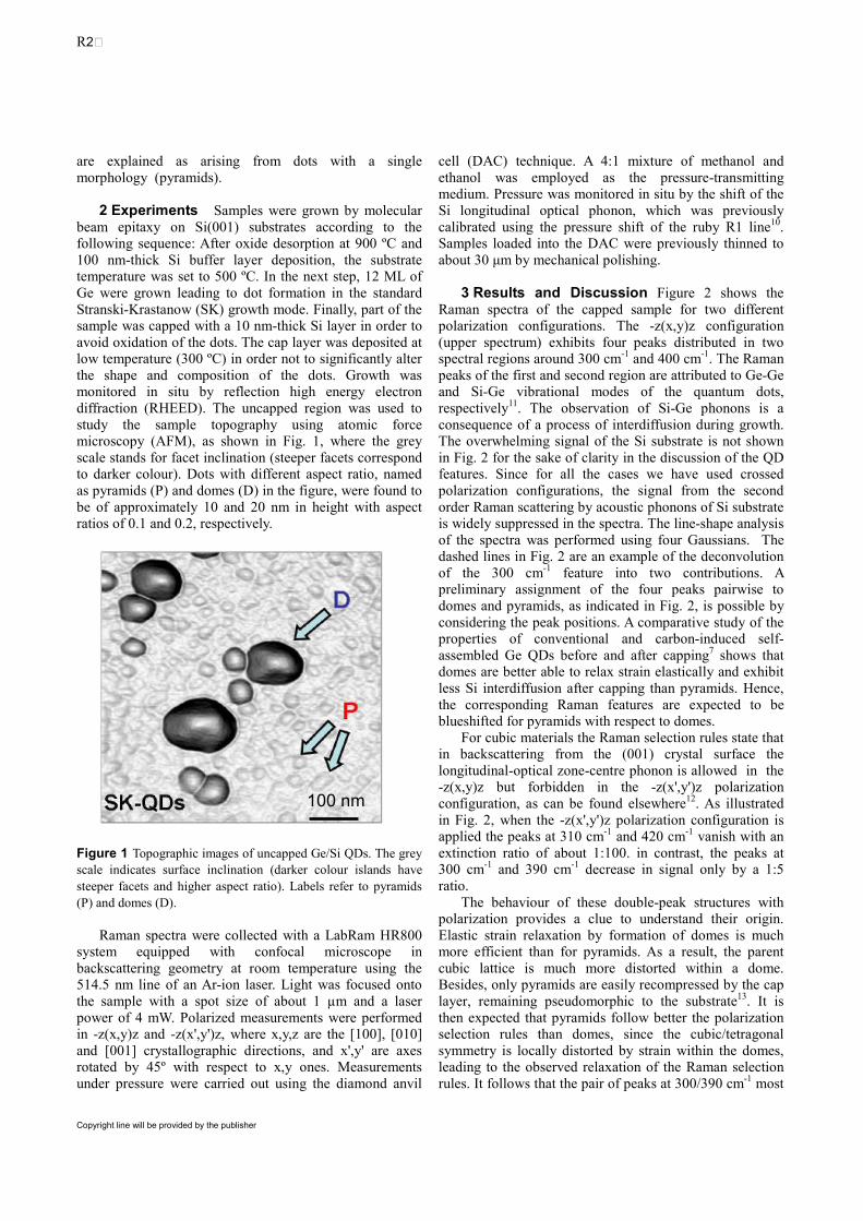
R2$
Copyright line will be provided by the publisher
are explained as arising from dots with a single
morphology (pyramids).
2 Experiments Samples were grown by molecular
beam epitaxy on Si(001) substrates according to the following sequence: After oxide desorption at 900 ºC and
100 nm-thick Si buffer layer deposition, the substrate temperature was set to 500 ºC. In the next step, 12 ML of
Ge were grown leading to dot formation in the standard
Stranski-Krastanow (SK) growth mode. Finally, part of the sample was capped with a 10 nm-thick Si layer in order to
avoid oxidation of the dots. The cap layer was deposited at low temperature (300 ºC) in order not to significantly alter
the shape and composition of the dots. Growth was monitored in situ by reflection high energy electron
diffraction (RHEED). The uncapped region was used to
study the sample topography using atomic force microscopy (AFM), as shown in Fig. 1, where the grey
scale stands for facet inclination (steeper facets correspond to darker colour). Dots with different aspect ratio, named
as pyramids (P) and domes (D) in the figure, were found to
be of approximately 10 and 20 nm in height with aspect ratios of 0.1 and 0.2, respectively.
Figure 1 Topographic images of uncapped Ge/Si QDs. The grey
scale indicates surface inclination (darker colour islands have
steeper facets and higher aspect ratio). Labels refer to pyramids
(P) and domes (D).
Raman spectra were collected with a LabRam HR800 system equipped with confocal microscope in
backscattering geometry at room temperature using the 514.5 nm line of an Ar-ion laser. Light was focused onto
the sample with a spot size of about 1 µm and a laser
power of 4 mW. Polarized measurements were performed in -z(x,y)z and -z(x',y')z, where x,y,z are the [100], [010]
and [001] crystallographic directions, and x',y' are axes rotated by 45º with respect to x,y ones. Measurements
under pressure were carried out using the diamond anvil
cell (DAC) technique. A 4:1 mixture of methanol and
ethanol was employed as the pressure-transmitting medium. Pressure was monitored in situ by the shift of the
Si longitudinal optical phonon, which was previously
calibrated using the pressure shift of the ruby R1 line10
. Samples loaded into the DAC were previously thinned to
about 30 µm by mechanical polishing.
3 Results and Discussion Figure 2 shows the
Raman spectra of the capped sample for two different polarization configurations. The -z(x,y)z configuration
(upper spectrum) exhibits four peaks distributed in two spectral regions around 300 cm
-1 and 400 cm
-1. The Raman
peaks of the first and second region are attributed to Ge-Ge and Si-Ge vibrational modes of the quantum dots,
respectively11
. The observation of Si-Ge phonons is a
consequence of a process of interdiffusion during growth. The overwhelming signal of the Si substrate is not shown
in Fig. 2 for the sake of clarity in the discussion of the QD features. Since for all the cases we have used crossed
polarization configurations, the signal from the second
order Raman scattering by acoustic phonons of Si substrate is widely suppressed in the spectra. The line-shape analysis
of the spectra was performed using four Gaussians. The dashed lines in Fig. 2 are an example of the deconvolution
of the 300 cm-1
feature into two contributions. A preliminary assignment of the four peaks pairwise to
domes and pyramids, as indicated in Fig. 2, is possible by
considering the peak positions. A comparative study of the properties of conventional and carbon-induced self-
assembled Ge QDs before and after capping7 shows that
domes are better able to relax strain elastically and exhibit
less Si interdiffusion after capping than pyramids. Hence,
the corresponding Raman features are expected to be blueshifted for pyramids with respect to domes.
For cubic materials the Raman selection rules state that in backscattering from the (001) crystal surface the
longitudinal-optical zone-centre phonon is allowed in the -z(x,y)z but forbidden in the -z(x',y')z polarization
configuration, as can be found elsewhere12
. As illustrated
in Fig. 2, when the -z(x',y')z polarization configuration is applied the peaks at 310 cm
-1 and 420 cm
-1 vanish with an
extinction ratio of about 1:100. in contrast, the peaks at 300 cm
-1 and 390 cm
-1 decrease in signal only by a 1:5
ratio.
The behaviour of these double-peak structures with polarization provides a clue to understand their origin.
Elastic strain relaxation by formation of domes is much more efficient than for pyramids. As a result, the parent
cubic lattice is much more distorted within a dome. Besides, only pyramids are easily recompressed by the cap
layer, remaining pseudomorphic to the substrate13
. It is
then expected that pyramids follow better the polarization selection rules than domes, since the cubic/tetragonal
symmetry is locally distorted by strain within the domes, leading to the observed relaxation of the Raman selection
rules. It follows that the pair of peaks at 300/390 cm-1
most
100 nm

phys. stat. sol. (a) 201, No. 13 (2004) / www.pss-rapid.com R3
Copyright line will be provided by the publisher
likely arises from the domes, whereas the pair at 310/420
cm-1
originates from the pyramids. We rule out that this depolarization effect arises
from refraction of the incident light entering the sample,
which is slightly deviated from normal incidence due to the fact that the surface of the sample is not flat, particularly
above the larger islands, i.e., domes. For this purpose we have grown a sample with similar domes but a much
thicker cap layer of approximately 300 nm. In this case the
sample surface is completely flat, thus, no deviation of the
300 400
x15
Intensity (arb. units)
Domes
Raman Shift (cm-1)
z(x,y)z
z(x',y')z
Ge QDs
514.5 nm
300 K
Pyramids
x5
Figure 2 Raman Spectra of the QDs sample using two different
polarization configurations: -z(x,y)z (upper), and -z(x',y')z
(lower). The spectra in the region of the Si-Ge mode are
multiplied by the given factors. Dashed lines represent the
deconvolution of the spectral line shape using Gaussians.
incident beam can occur. However, we obtained a similar depolarization in this case too, implying that the observed
effect is intrinsic to the domes.
As previously shown14, the QD strain status can a be
also studied by applying hydrostatic pressure and
measuring the pressure coefficient of the Ge-Ge mode arising from both types of dots. In Fig. 3 we show three
representative spectra for different pressures. As clearly observed, with increasing pressure the separation between
both Ge-Ge peaks (domes and pyramids) decreases. In
order to obtain the pressure coefficient of each dot ensemble type, we have restricted ourselves to the range
between 0 and 2 GPa where the pressure dependence of the phonon frequency is essentially linear. In the inset to Fig. 3
we display the obtained results to determine the pressure
coefficients. The points represent the position of the maximum of the Ge-Ge peak for the domes and pyramids
and the straight line is a linear fit to the experimental data. Unfortunately, it was not possible to obtain the pressure
coefficients of the Si-Ge modes because inside the DAC
the signal was too low to distinguish these peaks (see Fig. 3). In addition, it should be pointed out that the pressure
experiments were performed in strict backscattering
configuration, so that the strong Raman signal from the diamond at 1332 cm
-1 affects more the measurement of the
Si-Ge than the Ge- Ge mode.
The obtained linear pressure coefficients of the Ge-Ge mode are 3.30(20) and 3.60(5) cm
-1/GPa for pyramids and
domes, respectively. Numbers in parentheses represent error bars. Although these values are quite similar, the
difference is beyond experimental uncertainty. As shown
by Reparaz et. al.14
the pressure coefficient of dots decreases in magnitude as the dot-to-cap-layer volume
ratio decreases. Since the cap layer is the same for all dots in our sample, we expect that pyramids which are much
smaller than domes have a lower pressure coefficient. Hence, the pressure results confirm the assignment of the
Raman peaks already made based on the polarization
behaviour.
250 300 350 400 450
0.0 0.5 1.0 1.5
304
308
316
320
D
Raman Shift (cm-1)
Pressure (GPa)0.3 GPa
1.6 GPa
0.7 GPa
Intensity (arb. units)
Raman Shift (cm-1)
Ge QDs
514 nm
300 K
P
Figure 3 Pressure coefficient determination for the Ge-Ge
mode for pyramids and domes. Inset: The points indicate the
position of the measured peaks and the solid line is a linear fit of
the data.
Our observations are not compatible with the interpretation of the double-peak structures as arising from
the same QD ensemble but from different regions of the
same dot, as proposed by Valakh et. al.9, within the so
called core-shell model. In this model it is considered that
every QD consists of two distinct regions; a Ge-rich core and an outer intermixed shell, giving rise to two peaks in
the Raman spectra. The lower-frequency Ge-Ge component is ascribed to the intermixed shell together with
the most prominent Si-Ge peak at higher frequency. Our
measurements demonstrate, however, that these peaks display different polarization behaviour, invalidating the
assignment to the dot shell. Moreover, the same pressure coefficient is expected for core and shell region of the
same dot because at high Ge contents the pressure
coefficient is independent of composition8.
R4$
Copyright line will be provided by the publisher
3 Summary We have combined polarized Raman
spectroscopy with high pressure measurements to establish the origin of the double-peak structures at the frequencies
of the Ge-Ge and Si-Ge modes very often observed in self-
assembled Ge/Si dot samples. We have shown that the lower frequency peaks and the higher frequency ones of
the Ge-Ge and Si-Ge doublets are coupled to each other and that each of these pairs can be attributed to different
dot types, domes and pyramids, indicating the existence of
a bimodal size distribution. Our results are relevant for the interpretation of Raman spectra of quantum dot samples in
general since they are valid for any material system besides Si/Ge.
Acknowledgements J.S.R. Acknowledges financial support
from the AlBan fellowship Program. A.B. acknowledges an FPI
fellowship. This work was supported in part by the Spanish
Ministerio de Educación y Ciencia through grant MAT2006-
02680. Measurements were performed at the Nanotechnology
Laboratory of MATGAS 2000 A.I.E.
References
[1] J. Faist, F. Capasso, D. L. Sivco, C. Sirtori, A. L. Hutchinson
and A. Y. Cho, Science 264, 553 (1994).
[2] B. F. Levine, J. Appl. Phys. 74, R1 (1993).
[3] Y.-W. Mo, D. E. Savage, B. S. Swartzentruber, and M. G.
Lagally, Phys. Rev. Lett. 65, 1020 (1990).
[4] G. Medeiros-Ribeiro, A. M. Bratkovski, T. I. Kamins, D. A. A.
Ohlberg, and R. S. Williams, Science 279, 353 (1998).
[5] M. Stoffel, A. Rastelli, J. Stangl, T. Merdzhanova, G. Bauer, and
O.G. Schmidt, Phys. Rev. B 75, 113307 (2007). [6] J.S. Reparaz, A. Bernardi, A.R. Goñi, M.I. Alonso, and
M.Garriga, Appl. Phys. Lett. 91, 081914 (2007).
[7] A. Bernardi, M. I. Alonso, J. S. Reparaz, A. R. Goñi, P. D.
Lacharmoise, J. O. Ossó, and M. Garriga, Nanotechnol. 18,
475401 (2007). [8] J. S. Reparaz, A. Bernardi, A. R. Goñi, M. I. Alonso,
and M Garriga, Appl. Phys. Lett. 92, 081909 (2008).
[9] M.Y. Valakh, V. Yukhymchuk, V.M. Dzhagan, O.S. Lytvyn,
A.G. Milekhin, A.I. Nikiforov, O.P. Pchelyakov, F. Alsina, J.
Pascual, Nanotechnol. 16, 1464 (2005).
[10] H.K. Mao, J. Xu, and P.M. Bell, J. Geophy. Res. 91, 4673
(1986).
[11] M. I. Alonso and K. Winer, Phys. Rev. B 39, 10056 (1989).
[12] K. Mizoguchi and S. Nakashima, J. Appl. Phys. 65, 2583
(1989).
[13] B. V. Kamenev, H. Grebel, L. Tsybeskov, T. I. Kamins, R. S.
Williams, J. M. Baribeau, and D. J. Lockwood, Appl. Phys.
Lett. 83, 5035 (2003).
[14] J.S. Reparaz, A. Bernardi, A.R. Goñi, M.I. Alonso, and
M.Garriga, Appl. Phys. Lett. 91, 081914 (2007).

phys. stat. sol. (b) 244, No. 1, 76–81 (2007) / DOI 10.1002/pssb.200672543
© 2007 WILEY-VCH Verlag GmbH & Co. KGaA, Weinheim
Raman scattering of capped and uncapped carbon-induced
Ge dots under hydrostatic pressure
A. Bernardi*, J. S. Reparaz, A. R. Goñi**, M. I. Alonso, and M. Garriga
Institut de Ciència de Materials de Barcelona-CSIC, Esfera UAB, 08193 Bellaterra, Spain
Received 25 July 2006, accepted 8 August 2006
Published online 8 December 2006
PACS 62.50.+p, 63.22.+m, 78.30.Am, 78.67.Bf, 81.07.Ta
We compare results from Raman scattering for both capped and uncapped Ge quantum dots under hydro-
static pressure. The behavior of lattice vibrations and electronic transitions of the quantum dots are af-
fected by the presence or absence of a cap layer. The pressure coefficient obtained for the Ge mode of re-
laxed, uncapped islands is close to the corresponding value in bulk, whereas it is reduced by ∼20% in
presence of a Si cap layer. This result can be understood by taking into account the change of the bound-
ary condition imposed to the Ge lattice, which is constrained to match that of the silicon matrix. Meas-
urements of the capped sample exhibit a resonant enhancement which is not appreciable for the uncapped
dots. We relate this effect to the different lifetime of electronic states.
© 2007 WILEY-VCH Verlag GmbH & Co. KGaA, Weinheim
1 Introduction
Self-assembled Ge quantum dots (QDs) on Si(001) might, in the future, be considered as a candidate for
optoelectronic applications by controlling the built-in strain which, in turn, allows to tailor the optical
properties of nanostructures [1]. Raman scattering represents a powerful diagnostic tool to gather infor-
mation on composition and strain in thin films and quantum dots. Moreover, due to the different com-
pressibility of Si and Ge, experiments under hydrostatic pressure [2, 3] can also be used to tune the strain
induced by the silicon matrix on the embedded Ge dots and, as a result, a shift of their interband elec-
tronic transitions can be obtained [4, 5]. Previous works on Ge dots under pressure focused on samples
capped with thick layers (∼200 nm) and reported pressure coefficients (dω/dP) for the optical Ge mode
systematically lower than the value measured for the bulk material (3.9 cm–1/GPa) [6–8]. Such discrep-
ancy is discussed accounting for the different elastic properties of Ge and the surrounding silicon host
matrix [9].
In this work, we investigated the case of uncapped quantum dots and we demonstrate that if the com-
pression acting at the substrate/island interface (at the dot basis) is not affecting substantially the whole
volume of the island, then the measured pressure coefficient tends to the value of bulk Ge. On the con-
trary, a really thin (10 nm) Si cap-layer is enough to achieve an important reduction (by ∼20%) of the
pressure coefficient, in analogy with data of the literature obtained for much thicker cap layers. More-
over, the presence of a thin cap layer enables the resonant enhancement of Raman scattering intensity to
be observed, when an interband electronic transition of the Ge QDs is brought into resonance with the
laser line by applying pressure. This effect is otherwise not detectable in uncapped samples due to a
reduced lifetime of electronic states.
* Corresponding author: e-mail: [email protected], Fax: +34 93 580 57 29
** ICREA Research Professor

phys. stat. sol. (b) 244, No. 1 (2007) 77
www.pss-b.com © 2007 WILEY-VCH Verlag GmbH & Co. KGaA, Weinheim
Original
Paper
2 Experimental details
Samples were grown by solid-source molecular beam epitaxy according to the following procedure: after
oxide desorption at 900 °C and 50 nm-thick Si buffer layer deposition, a 4Å∼ thick Ge wetting layer
was grown before depositing 0.1 monolayers (MLs) of carbon. This surface modification allows for the
control of shape and density ( 9 23 10 cm∼
-
¥ ) of islands in the next growth step, when 6Å∼ of Ge are
deposited at 500 °C. The resulting topography consists of dome-shaped dots 10–15 nm high [10]. For
the capped sample, a 10 nm thick Si layer was subsequently grown at low temperature (300 °C) in order
to avoid silicon intermixing and to preserve the island shape.
The Raman spectra were collected with a LabRam HR800 system in backscattering geometry at room
temperature using different lines from an argon-ion laser. Measurements under pressure were carried out
using the diamond anvil cell (DAC) technique. A 4:1 mixture of methanol and ethanol was employed as
the pressure-transmitting medium. Pressure was monitored in situ by the shift of the ruby R1 line [12].
The samples loaded in the DAC were previously thinned to about 30 microns by mechanical polishing.
3 Results and discussion
3.1 Vibrational modes
Figure 1 shows Raman spectra measured at various pressures up to ∼7 GPa in the capped sample. The
Raman signal close to 1300 cm∼
- is ascribed to the Ge–Ge phonon mode of the Ge dots. We note that
these spectra were measured in crossed polarization ( )z x y z, , where x, y, and z are the [100], [010], and
[001] crystallographic directions of the Si substrate, in order to suppress the second-order Raman signal
of the transverse acoustical phonons of the Si substrate, which would interfere with the Ge dot mode.
The very strong signal at 1520 cm∼
- is attributed to the optical phonon of the Si substrate. Both modes
shift to higher frequencies with increasing pressure and their intensities change due to resonance effects.
The intensity decrease of the substrate mode is related to the shift of the 1
E electronic transition of Si to
higher energies with increasing pressure.
The overall intensity of the spectra in the uncapped sample is much lower than for the capped one and
no polarization analysis was made. However, the Ge–Ge mode and second order Si-2TA signal that al-
most overlap each other at 0P = can be resolved under pressure, since they shift in opposite directions [7].
The frequency shift of the strong Si substrate signal at 1520 cm∼
- can be used as internal wavenumber ca-
libration of the spectra. The Raman shifts measured as a function of pressure are plotted in Fig. 2. A linear
fit to the data gives the pressure coefficient 1d /d (3 9 0 1) cm /GPaPω-
= . ± . and the phonon frequency at
250 300 350 500 550
Si-Si
Capped Ge QDs
488 nm
300 K
6.1
1.3
5.1
6.7
3.5
2.3
Inte
nsity (
arb
. u
nits)
Raman Shift (cm-1)
Ge-GeP [GPa]
X 0.2
Fig. 1 Raman spectra of the capped QDs measured at
different pressures. The peak at 1300 cm∼
- (ambient pres-
sure value) corresponds to the Ge–Ge phonon, whereas
the very strong signal at 1520 cm∼
- comes from the Si
substrate.

78 A. Bernardi et al.: Raman scattering of capped and uncapped carbon-induced Ge dots
© 2007 WILEY-VCH Verlag GmbH & Co. KGaA, Weinheim www.pss-b.com
0 1 2 3 4 5
305
310
315
320
Uncapped
Capped
Ge QDs
514.5 nm
300 K
Ram
an S
hift
(cm
-1)
Pressure (GPa)
zero pressure 1
0301 5 0 2 cmω
-
= . ± . for the uncapped sample, and 1d /d 3 30 0 02 cm /GPaPω
-
= . ± . and 1
0303 94 0 04 cmω
-
= . ± . for the capped sample. The values of 0
ω are different due to an increase in built-
in strain for the capped QDs with respect to the relaxed, uncapped ones.
The pressure coefficient obtained for the uncapped sample is in very good agreement with the ex-
pected Ge bulk value. However, for the sample capped with 10 nm of Si we obtain instead a lower coef-
ficient which is closer to the values reported for dots overgrown with much thicker Si cap-layers [7] or in
superlattices [8].
The carbon-induced Ge dots under investigation are Ge rich (>90%) dome-shaped islands [10, 11],
whose enhanced aspect-ratio leads to an efficient relaxation of the strain originating at the is-
land/substrate interface due to the lattice mismatch between Ge and Si (∼4%). Raman scattering spec-
troscopy gives information on the average Ge content and mean strain of the islands. In particular, the
Ge–Ge mode is likely to steam mainly from the Ge-rich core of the islands, where holes are better con-
fined. We thus expect that only a small contribution corresponds to the volume of material close and
elastically coupled to the silicon substrate, for example, the wetting layer.
The different pressure coefficients obtained for samples with and without cap layer can be explained if
we consider the boundary conditions applicable for each case. In general, the strain induced on the dot by
applying external pressure can be decomposed in two terms:
hydro matrix( ) ( ) ( )P P Pε ε ε= + , (1)
where the first term is the pure hydrostatic part of the Ge dot described by the Murnaghan equation of
state ( Ge
0B is the bulk modulus of Ge)
0
1Ge Ge 3
hydro 0 0
Ge Ge Ge
0 0 0
( )( ) 1 1 . . .
3
Ba P a B PP P
a B Bε
-¢- ¢Ê ˆ= = + + @ - +Á ˜Ë ¯
(2)
When the dot is constrained into a host material the additional term accounts for the strain originating
from the different compressibility of the dot and matrix material. It depends on the boundary condition
which we express in terms of a parameter 0 1ϕ< < to describe the degree of relaxation of the dot accord-
ing to
QD Gematrix
Ge
0
QD SiSi Ge Si Ge
Ge QD Ge0
( ) ( )( )
0[ ( ) ( ( ) ( ))] ( )
1 .
a P a PP
a
a aa P a P a P a P
a a a
ε
ϕϕ
ϕ
ÏÔÌÔÓ
-=
= , =+ - -=
= , =
Fig. 2 Position of the Raman peaks observed in the two
samples as a function of pressure. Open (closed) circles
are results of the capped (uncapped) sample. Solid lines
correspond to least-squares fits to the experimental data
using a linear function.
(3)

phys. stat. sol. (b) 244, No. 1 (2007) 79
www.pss-b.com © 2007 WILEY-VCH Verlag GmbH & Co. KGaA, Weinheim
Original
Paper
Combining Eqs. (1)–(3) we can obtain a general expression for the expected Raman frequency shift
under pressure, with a constant term representing the shift due to the built-in strain (at applied pressure
P = 0) and a linear term on P, whose slope is the pressure coefficient of the phonon mode (here ijK are
the phonon deformation potentials for Ge):
( ) ( ) ( ) ( )
( )
Si Ge
0 0 0 0
11 12 11 12 Ge
0
0
11 12 Si Ge Si
0 0 0
2 2 12 2
1 1 12 .
6
a aK K P K K
a
K K PB B B
ω ωω ε ϕ
ωϕ
-È ˘D = + ª + -Í ˙Î ˚È Ê ˆ ˘- + + -Á ˜Í ˙Ë ¯Î ˚
If we consider the sample with uncapped QDs and we assume that due to strain relaxation the average
lattice parameter in the dot is QD Gea aª (corresponding to the case 1ϕ ª ), then there is no built-in strain
and the pressure coefficient is given by the pure hydrostatic term, dependent on the bulk modulus of Ge.
When a cap layer is present, the dot is compressed to adjust its lattice parameter to that of the host mate-
rial, i.e. QD Sia aª (if the dot is fully compressed then 0ϕ ª ). In this second case, as deduced from
Eq. (4), only the bulk value of silicon enters in the calculation of the pressure coefficient and a constant
frequency shift is arising from the built-in strain. From Eq. (4) follows that ( ) ( )capped uncapped
d /d / d /dP Pω ω Ge Si
0 0/ 0 77B B= = . , in good agreement with the experimental value (0.84).
3.2 Electronic states
The influence of pressure on the 1
E and 1 1
E ∆+ electronic transitions of the QDs can be studied by reso-
nant Raman measurements [13, 14]. When the energy of the exciting laser is close to that of the optical
transitions, the resonance curve can be tuned by pressure. In our experiments we were able to measure a
resonant enhancement of the Ge–Ge Raman phonon only on the sample with cap layer. The Raman
intensity on the uncapped sample was rather low and remained constant within noise. This fact seems
contradictory because these electronic transitions were measured by ellipsometry on the uncapped sam-
ple at 1
2 23E = . eV and 1 1
2 43E ∆+ = . eV and are in the suitable spectral range. According to these ener-
gies, the QDs have an average composition 0 92x = . [10]. The Ge transition energies on the capped sam-
ple cannot be fitted clearly due to absorption by the Si cap, nevertheless, the QD composition should not
be altered by the low T capping process. In order to understand the different resonance behavior
with/without cap layer, we have modeled the shape and relative intensity of the two resonance curves by
considering the expression of the Raman polarizability near the two-dimensional critical points 1
E and
1 1E ∆+ [15]:
1 1 1 1 1 1
25
1 02 5
3 0
1 1
( )| |
d4 2
E E E Ed d
a dE
∆ ∆χ χ χ χ
∆
+ +
,
,
Ê ˆ+ -µ - ,Á ˜Ë ¯
22
2e ln 1 ,j jE i j
j
j j
E EA
E E i
φχ
Γ
È ˘Ê ˆ= -Í ˙Á ˜-Ë ¯Í ˙Î ˚
where jE
χ is the electronic susceptibility and the critical-point parameters are the amplitude jA , the width
jΓ and the phase jφ . The latter are obtained from analysis of ellipsometric spectra. The pressure-tuned
resonance curve is obtained at fixed laser energy L
2 541E E= = . eV. To introduce the dependence on
pressure we take into account that both gaps shift with the same pressure coefficient α , that is,
( ) (0)j jE P E Pα= + . In this way, the pressure coefficient α can be evaluated from measurements using
only one laser line.
The results for the resonant enhancement of the Ge-mode intensity for the capped sample are plotted
in Fig. 3. Raman intensities are normalized relative to the maximum intensity at resonance and are given
in arbitrary units. We fit the shape of the curve as a function of pressure having α as fit parameter. The
(5)
(4)

80 A. Bernardi et al.: Raman scattering of capped and uncapped carbon-induced Ge dots
© 2007 WILEY-VCH Verlag GmbH & Co. KGaA, Weinheim www.pss-b.com
0
1
0 5 10
Ram
an in
tens
ity (
arb.
uni
ts)
Pressure (GPa)
CGe QDs
( xGe = 0.92)
EL = 2.541 eV
α = 40 meV/GPa
E1E1 + ∆1
experimentfit (with cap)
calc. (no cap)
actual transition energies are calculated from the known composition 0 92x = . and with a best-fit built-in
biaxial strain 0 6%ε = - . . The rest of the needed quantities are taken from literature values for Ge [15].
In particular, the broadening of the gaps are taken as those of bulk Ge. For the uncapped sample, the
broadening obtained from ellipsometry is about a factor of two larger. If we just calculate the resonance
curve expected for the uncapped sample with larger broadening, the overall Raman intensity drops con-
siderably, as shown in Fig. 3 by the dotted curve.
The value of 40 5α = ± meV/GPa obtained from the fit is similar to previous measurements in capped
samples, reduced with respect to bulk Ge in the same way as the phonon pressure coefficient. It is likely
that α in the uncapped sample should be closer to the bulk value but, unfortunately, it was not possible to
be evaluated.
4 Conclusions
In this work we compared Raman scattering from Ge QDs under hydrostatic pressure when the dots are
uncapped versus the situation where they are covered with a Si cap layer. We demonstrated that if the
dots are not embedded in the Si matrix, then the measured pressure coefficient tends to the value of bulk
Ge. On the contrary, just a very thin 10 nm Si cap layer is sufficient to reduce the coefficient by ∼20% to
values similar as previously obtained in literature for much thicker cap layers.
We considered the different boundary conditions to explain these two experimental situations, namely
we dealt with the limiting cases of fully relaxed uncapped dots (highest d /dPω ) and fully compressed
capped dots (lowest d /dPω ). Nevertheless, Eq. (4) also holds for a much more complex and generalized
scenario, where an intermediate situation can be accounted for. Depending on the shape (aspect ratio)
and on the size of the dots the degree of relaxation (ϕ ) is expected to vary considerably and the DAC
technique for the determination of pressure coefficients turns out to be a powerful diagnostic tool for
studying the mechanisms of relaxation in self-assembled nanostructures.
Moreover, we observed that in uncapped dots no significant resonant enhancement of Raman scatter-
ing intensity can be observed, an effect clearly seen in presence of a thin cap layer. The increased life-
time (smaller broadening) of electronic states in capped samples is considered as a plausible explanation
for this observation.
Acknowledgments We thank the spanish Ministerio de Educación y Ciencia for support through MAT2003-
00738 and an FPI fellowship (A.B.). J.S.R. acknowledges an Alßan fellowship.
Fig. 3 Resonant Raman intensities of the Ge–Ge mode as a
function of pressure for the capped dot sample (symbols). The
solid (dotted) line is the calculated resonance curve for the
capped (uncapped) dots, as explained in the text. Arrows indi-
cate the pressure values for which the laser of energy L
E coin-
cides with the corresponding optical transition.
phys. stat. sol. (b) 244, No. 1 (2007) 81
www.pss-b.com © 2007 WILEY-VCH Verlag GmbH & Co. KGaA, Weinheim
Original
Paper
References
[1] J. Stangl, V. Holy, and G. Bauer, Rev. Mod. Phys. 76, 725 (2004).
[2] Z. Sui, H. H. Burke, and I. P. Herman, Phys. Rev. B 48, 2162 (1993).
[3] Z. Sui, I. P. Herman, and J. Bevk, Appl. Phys. Lett. 58, 2351 (1991).
[4] Z. X. Liu, O. G. Schmidt, U. D. Venkateswaran, K. Eberl, and K. Syassen, Semicond. Sci. Technol. 15, 155
(2000).
[5] K. L. Teo, S. H. Kwok, P. Y. Yu, and S. Guha, Phys. Rev. B 62, 1584 (2000).
[6] M. Seon, M. Holtz, T.-R. Park, O. Brafman, and J. C. Bean, Phys. Rev. B 58, 4779 (1998).
[7] K. L. Teo, L. Qin, Z. X. Shen, and O. G. Schmidt, Appl. Phys. Lett. 80, 2919 (2002).
[8] L. Qin, K. L. Teo, Z. X. Shen, C. S. Peng, and J. M. Zhou, Phys. Rev. B 64, 075312 (2001).
[9] L. Liu, K. L. Teo, Z. X. Shen, J. S. Sun, E. H. Ong, A. V. Kolobov, and Y. Maeda, Phys. Rev. B 69, 125333
(2004).
[10] A. Bernardi, J. O. Ossó, M. I. Alonso, A. R. Goñi, and M. Garriga, Nanotechnology 17, 2602 (2006).
[11] A. Bernardi, M. I. Alonso, A. R. Goñi, J. O. Ossó, and M. Garriga, Appl. Phys. Lett. 89, 101921 (2006).
[12] H. K. Mao, J. Xu, and P. M. Bell, J. Geophy. Res. 91, 4673 (1986).
[13] D. Bougeard, P. H. Tan, M. Sabathil, P. Vogl, G. Abstreiter, and K. Brunner, Physica E 21, 312 (2004).
[14] A. B. Talochkin, S. A. Teys, and S. P. Suprun, Phys. Rev. B 72, 115416 (2005).
[15] M. I. Alonso and M. Cardona, Phys. Rev. B 37, 10107 (1988).

3.2.3 Conclusions
A new method to determine the strain status of quantum dot systems waspresented. An important advantage of this method is that it is independentof the studied material system. In particular, it was used to study the strainstatus of Ge/Si dots as a function of the Si cap layer thickness. It was foundthat the Ge dots undergo a biaxial to hydrostatic strain status transitionwhen increasing the Si cap layer thickness (critical thickness ∼ 10 nm). Thisis an important result since it provides a guide for an appropriate choice ofthe strain tensor in each particular situation.
This technique was also applied to a system with a bimodal distributionof Ge/Si dots. A different strain status was found for each dot distributionreflected in a different pressure coefficient. This provides an alternative ex-planation for the doulbe-peak structure often observed in Raman spectra ofsemiconductor QDs in clear contrast with the so-called core-shell model[12].
The presented method has proved to be appropriate to study the strainstatus of certain low dimensional structures. The optical phonon pressurecoefficient determination, thus, provides a direct measurement of the strainstatus of these structures that would be rather complicated to perform usingother techniques.


Bibliography
[1] S. Christiansen, M. Albrecht, H. P. Strunk, and H. J. Maier, Appl. Phys.Lett 64, 3617 (1994).
[2] F. Liu S. E. Davenport, H. M. Evans, and M. G. Lagally, Phys. Rev.Lett. 82, 2528 (1999), and references therein.
[3] V. Le Thanh, V. Yam, P. Boucaud, F. Fortuna, C. Ulysse, D. Bouchier,L. Vervoort, and J.-M. Lourtioz, Phys. Rev. B 60, 5851 (1999).
[4] A. A. Darhuber, P. Schittenhelm, V. Hol, J. Stangl, G. Bauer, and G.Abstreiter, Phys. Rev. B 55, 15652 (1997).
[5] O. G. Schmidt and K. Eberl, Phys. Rev. B 61, 13 721 (2000)
[6] O. G. Schmidt, K. Eberl, and Y. Rau, Phys. Rev. B 62, 16 715 (2000).
[7] M. A. Makeev, and A. Madhukar, Phys. Rev. Lett. 86, 5542 (2001).
[8] C. Pryor, J. Kim, L. W. Wang, A. J. Williamson, and A. Zunger, J. Appl.Phys. 83, 2548 (1998).
[9] K. L. Teo, L. Qin, I. M. Noordin, G. Karunasiri, Z. X. Shen, O. G.Schmidt, K. Eberl, and H. J. Queisser, Phys. Rev. B 63, 121306(R) (2001).
[10] A. Bernardi, J. S. Reparaz, A. R. Goni, M. I. Alonso, and M. Garriga,phys. stat. sol. (b) 244, 76 (2007).
[11] J. S. Reparaz, A. Bernardi, A. R. Goni, M. I. Alonso, and M. Garriga,Appl. Phys. Lett. 92, 081909 (2008).
[12] M. Y. Valakh, V. Yukhymchuk, V. M. Dzhagan, O. S. Lytvyn, A. G.Milekhin, A. I. Nikiforov, O. P. Pchelyakov, F. Alsina, J. Pascual, Nan-otechnol. 16, 1464 (2005).
57


3.3 Strain Effect in CdSe Quantum Dots
Compound semiconductors of the II-VI family have been widely studied dueto their potential applications in the optoelectronic industry. The advantageof these materials, in contrast to the III-V compounds, is their higher excitonbinding energy and the wider energy band gap that they offer. In particu-lar, self-assembled QDs are good candidates since they also provide spatialconfinement of the excitons within the QDs. A great amount of work can befound in the literature for this system, like CdSe/ZnMnSe, CdSe/ZnBeSe,ZnCdSe/ZnSe, CdTe/ZnTe, and ZnSe/ZnS (see Refs. [1]-[9]). However, thecontrol and reproducibility in the size of the QDs continue to be a drawbackregarding future device applications. In this section, a recently developedsystem will be presented, whose mayor advantage is an improvement in thecontrol and reproducibility of the QD size distribution. It will be furthershown that by combining Raman spectroscopy with high pressure measure-ments its possible to obtain information about the strain status of this systemtoo.
3.3.1 Motivation and Previous Work
In this section a brief introduction to a recently developed II-VI QDs systemwill be provided. Raman spectroscopy and high pressure measurements wereused as characterization techniques. It is not the author’s purpose to makea review of this field but instead to give a short description of the previouslyinvestigated physical properties of the studied samples. As was already men-tioned, a major drawback of II-VI systems is the low degree of control andreproducibility of the QD size as compared to other systems like III-V com-pounds. In a recent publication [1] Perez-Paz et. al. presented a systemwith a high degree of reproducibility concerning its growth mechanism. Thestudied samples were CdSe QDs with Zn0.38Cd0.23Mg0.39Se barriers grown bymolecular beam epitaxy. Fig. 3.8 shows the structure of the samples as wellas a typical AFM image extracted from Ref. [1]. The QD height rangesbetween 3 and 7 monolayers (ML) of CdSe and the barrier is the same forall the cases.
Fig. 3.9 shows the PL spectra for five samples with different CdSe de-position times: 6 s (1.2 ML), 13 s (2.5 ML) , 18 s (3.6 ML), 24 s (4.8 ML),and 29 s (5.8 ML). The ZnCdMgSe barrier layers were grown with the samecomposition, thickness, and band gap of about 2.8 eV for all the samples.The nearly linear relation between the PL peak energy and the depositiontime (tD) is also shown in Fig. 3.9. Several sets of samples grown on differentdays indicate that a good control and reproducibility were achieved (different
59

Results and Discussion
a) b)
Figure 3.8: a) Sketch of the structure of the studied samples. b) TypicalAFM image of CdSe dots with ZnCdMgSe barriers. The inset shows anhistogram of the QD height. Extracted from Ref. [1].
points in Fig. 3.9, left).As we have seen from the work of Perez-Paz et. al. this system allows
for a tunning of the optical emission in almost all the visible range. In orderto study the influence of the built-in strain on the optical properties the twofollowing points were studied:
• Is built-in strain important concerning the tuning of the emission ofthe QDs? If this is the case, what is the contribution of this effect?
• How does the strain status of the dots depend on the dot size?
The influence of the built-in strain on the optical emission resulted in thepublication presented in the next section: “Size-dependent strain effects inself-assembled CdSe quantum dots with Zn0.38Cd0.23Mg0.39Se barriers” (Arti-cle Number: 5). In this article the built-in strain of the QDs was determinedand, thus, its influence on their optical properties. Interdiffusion of Mg from
60

Figure 3.9: Left: PL spectra of five samples grown with different depositiontime (tD). The PL peak emission energy and tD for each sample is indicatedin parentheses. Right: (a) Variation of the PL emission energy and (b) ofFWHM with tD for several samples grown on different days. The differentsymbols indicate the different days the samples were grown. Extracted fromRef. [1].
the barrier into the QDs was detected and quantified. The second point wasstudied in a second article presented in the next section: “Photoluminescenceof CdSe quantum dots with Zn0.38Cd0.23Mg0.39Se barriers under hydrostaticpressure” (Article Number: 6), where the pressure coefficient of the funda-mental emission of dots with different height was studied.
61


3.3.2 Experiments and Results
Article n: 5
Title: Size-dependent strain effects in self-assembled CdSe quan-tum dots with Zn0.38Cd0.23Mg0.39Se barriers.
Authors: J. S. Reparaz, A. R. Goni, M. I. Alonso, M. N. Perez-Paz, and M. C. Tamargo.
Journal: Applied Physics Letters
Article n: 6
Title: Photoluminescence of CdSe quantum dots withZn0.38Cd0.23Mg0.39Se barriers under hydrostatic pressure.
Authors: J. S. Reparaz, A. R. Goni, M. I. Alonso, M. N. Perez-Paz, and M. C. Tamargo.
Journal: Physica Status Solidi b
63


Size-dependent strain effects in self-assembled CdSe quantum dotswith Zn0.38Cd0.23Mg0.39Se barriers
J. S. Reparaz,a A. R. Goñi, and M. I. AlonsoInstitut de Ciència de Materials de Barcelona-CSIC, Esfera UAB, 08193 Bellaterra, Spain
M. N. Perez-Paz and M. C. TamargoDepartment of Chemistry, City College of The City University of New York, New York, New York 10031
Received 14 August 2006; accepted 25 October 2006; published online 6 December 2006
From resonant Raman scattering measurements under hydrostatic pressure the authors were able toidentify both the strain-shifted longitudinal optical phonon of CdSe quantum dots with differentaverage size embedded in a quaternary ZnCdMgSe material and a Mg-local dot mode due tointerdiffusion from the barrier. They show that the large tunability of the light emission, whichcovers most of the visible spectrum, is not only due to a different degree of confinement but also toa size-dependent built-in strain. The frequency of the Mg mode allowed them also to roughlyestimate the amount of Mg interdiffusion into the quantum dots. © 2006 American Institute ofPhysics. DOI: 10.1063/1.2402881
Strain-driven low-dimensional heterostructures of groupII-VI semiconductors have been extensively studied becauseof their potential applications in optoelectronics. In particu-lar, quantum dot QD structures are expected to lead to im-provement in the performance of light emitting diodes andsemiconductor lasers.1 Important advances in the fabricationof these zero-dimensional structures have been obtained us-ing different methods.2,3 The CdSe/ZnCdMgSe system, forinstance, is particularly attractive due to its intense photolu-minescence PL even at room temperature and the wide en-ergy range it offers to tune the QD emission. Recently, greatprogress has been achieved in the degree of control and re-producibility of the growth process by introducing Mg intothe barrier material.4 In this way, dots with unimodal sizedistributions are obtained, in which the average dot size andhence the emission energy of the CdSe QDs can be easilyadjusted by varying the CdSe deposition time. Furthermore,the large gap-energy difference of 1 eV between CdSe andthe quaternary barrier material allows for the tuning of theQD PL throughout the visible spectrum from the red to theblue.
In this letter we show how we made explicit use of theresonant enhancement of the Raman scattering signal toidentify vibrational modes stemming from CdSe/ZnCdMgSeQDs of different sizes, from which we were able to deter-mine the built-in strain and degree of Mg interdiffusion intothe dots. Different laser lines were brought into resonancewith the fundamental optical transition of the CdSe dots byapplying high hydrostatic pressures up to 6 GPa. An impor-tant result concerns the observation of size-dependent straineffects from which follows that the band-gap tunability ofthe CdSe/ZnCdMgSe dot system is due to a non-negligiblepart of at least 18% to the reduction of the built-in strain withdecreasing average dot size.
The CdSe/ZnCdMgSe samples were grown by molecu-lar beam epitaxy on InP 001 substrates. First a 150 nmthick lattice-matched InGaAs buffer layer was deposited fol-lowed by a Zn exposure for later reduction of the defectdensity in the ZnCdMgSe barrier. A 6 nm ZnCdSe layer is
used to promote the two-dimensional nucleation after which400 nm of Zn0.38Cd0.23Mg0.39Se was grown as barrier mate-rial. Finally, pure CdSe is deposited for dot growth in theStranski-Krastanow mode followed by another 130 nm bar-rier of Zn0.38Cd0.23Mg0.39Se. A 6 nm ZnCdSe cap layer wasused to prevent the oxidation of the barrier material. Theaverage base radius of the QDs is about 47 nm, whereas theirheight is ranging between 3 and 15 nm depending on theCdSe deposition time. The QD density is about7108 cm−2. Here we present data from two samples withdeposited thicknesses of 3.6 and 5.9 ML of CdSe and roomtemperature emission peaking at 2.23 and 2.03 eV, respec-tively. More details of the sample growth and their structuralcharacterization are given elsewhere.4
Resonant Raman measurements were performed in back-scattering geometry using two different laser lines for exci-tation, 514.5 and 632.5 nm. Spectra were acquired with aLabRam HR800 micro-Raman system. In order to meet reso-nance conditions in the different samples we applied highhydrostatic pressures using the standard diamond anvil cellDAC technique. Spectra under pressure were measuredwith crossed linear polarization to suppress the reflected laserbeam from the DAC. A 4:1 mixture of methanol and ethanolwas employed as pressure-transmitting medium. Pressurewas monitored in situ by the shift of the ruby R1 line.5 Thesamples loaded in the DAC were previously chemicallyetched to a thickness of about 1 m. An etchant solution of3:2 HCl to H3PO4 was used to selectively etch away the InPsubstrate.
Figure 1 shows Raman scattering spectra of samples Aand B with nominally 3.6 and 5.9 ML of CdSe, respectively,measured at ambient temperature and pressure conditions us-ing the red 1.96 eV and green 2.41 eV laser lines forexcitation. Up to four peaks are apparent in Raman spectra,from which the one at around 220 cm−1 and the broader peakcentered slightly above 300 cm−1 are identified as thelongitudinal-optical LO phonon of the CdSe dots and a Mglocal mode also from the QDs, respectively. This assignmentis based on the fact that the LO CdSe mode is only observedunder near resonance conditions of the laser with the funda-mental PL emission from the dots, which is attained with theaElectronic mail: [email protected]
APPLIED PHYSICS LETTERS 89, 231109 2006
0003-6951/2006/8923/231109/3/$23.00 © 2006 American Institute of Physics89, 231109-1Downloaded 08 Jan 2007 to 158.109.18.63. Redistribution subject to AIP license or copyright, see http://apl.aip.org/apl/copyright.jsp

green line for sample A and with the red line for sample B, asillustrated in Fig. 1. The 300 cm−1 Mg-local mode is alsoobserved together with the 220 cm−1 peak for 514.5 nm ex-citation laser line, which suggests that Mg from the barrier ispresent inside the QDs. Although this peak is not observedwhen exciting with the red laser line, pressure measurementssupport this hypothesis. In contrast, both modes are absent inthe Raman spectra of a control sample without CdSe dots butcontaining the barrier material, independently of the laserwavelength used for excitation. The peak at 235 cm−1, whichclearly resonates with green excitation in both samples, isattributed to the ZnSe-like LO mode of the 6 nm thickZnCdSe cap layer, whereas the nonresonant Raman peak at272 cm−1 corresponds to the GaAs-like LO phonon of theInGaAs buffer layer. We point out that the Raman selectionrules measured with linearly polarized light at ambient pres-sure conditions are consistent with the previous assignmentof the peaks.
In order to fully settle the issue of the identification ofQD Raman modes, we have fine-tuned the fundamental PLemission of sample A to the energy of the 514 nm laser lineby applying high hydrostatic pressure up to 6 GPa. In Fig. 2we display several Raman spectra measured at small pressuresteps in the range from 0.8 to 3.4 GPa. The broad band,which in this representation of the spectra as a function ofrelative wave numbers, shifts with increasing pressure to-wards the laser line corresponds to the PL emission from theCdSe dots. This is due to the strong increase with pressure ofthe energy of the fundamental optical transition of the dotswith a slope of about 47 meV/GPa.6 The only Raman peakswhich resonate with the PL emission from the CdSe dots arethe two ones previously assigned to the LO CdSe mode ataround 220 cm−1 and the Mg-local mode near 300 cm−1.Their Raman intensity is not only comparable to that of thedot PL but it also increases as these modes become more inoutgoing resonance with the PL band, as the applied pressureincreases. Interestingly, we observe a third Raman peak ataround 520 cm−1 at low pressure, which is also in outgoingresonance with the CdSe QD emission see Fig. 2. We be-lieve that this Raman peak corresponds to exciton-mediatedmultiphonon scattering by a combination of the LO CdSe
and the Mg-local mode due to strong electron-LO-phononcoupling in the highly polar II-VI compounds.7
Valuable information about the strain status of the CdSedots is obtained from a quantitative analysis of the frequencyand its pressure dependence of the QD vibrational modes. InFig. 3 we have plotted for sample A the peak position of bothQD phonon modes as a function of the applied pressure. Thesolid lines represent the result of least-squares fits to the datapoints using linear functions yielding
LO-CdSe = 2191 cm−1 + 5.43cm−1
GPa P , 1
Mg-local = 3012 cm−1 + 7.58cm−1
GPa P , 2
where P is the external hydrostatic pressure in GPa. Thelarge difference in the pressure slopes is only apparent andalmost vanishes after normalization by the mode frequencyto calculate the mode Grüneisen parameter according toi=−B0 /i0i /P, where B0=53 GPa is the bulk
FIG. 1. Color online Polarized Raman spectra at ambient pressure andtemperature conditions of samples A and B with nominally 3.6 and 5.9 MLof CdSe, respectively, using the red 632.5 nm and green 514.5 nm laserlines for excitation.
FIG. 2. Color online Evolution of the luminescence and resonant Ramanpeaks with hydrostatic pressure for sample A using the 514.5 nm laser linefor excitation. The five spectra correspond to the pressure values: 0.8, 1.0,1.8, 2.1, and 3.4 GPa.
FIG. 3. Pressure dependence of the mode frequencies in sample A for theLO CdSe and Mg-local modes. The different values quoted at zero pressurefor the Mg-local mode correspond to spectra measured outside the DACwith the four possible configurations of the linear polarization of incidentand scattered beams.
231109-2 Reparaz et al. Appl. Phys. Lett. 89, 231109 2006
Downloaded 08 Jan 2007 to 158.109.18.63. Redistribution subject to AIP license or copyright, see http://apl.aip.org/apl/copyright.jsp

modulus of CdSe Ref. 8 and i0 is the mode frequency incm−1 at zero pressure. For the LO CdSe and the Mg-localmode of the dots we obtain =1.30±0.08 and=1.32±0.12, respectively. The peak position of the broadband corresponding to the Mg-local mode at ambient pres-sure ranges from 300 to 305 cm−1 depending on the linearpolarization configuration see Fig. 3. The lower frequenciesare obtained with crossed polarization, as for the Ramanmeasurements under pressure, explaining why extrapolatedvalue from the fit to the pressure data points at P=0 is at301 cm−1.
Both the frequency of the Mg-local mode at zero pres-sure and the coincidence of its Grüneisen parameter with thatof the LO phonon indicate a low degree of Mg interdiffusionfrom the quaternary barrier into the nominally pure CdSedots. Using a modified linear diatomic-chain model for thecalculation of the Mg local-mode frequency in a zinc blendeCdSe and ZnSe host9 and by comparing with the only avail-able data for Zn1−xMgxSe alloys,10 the zero-pressure fre-quency of 305 cm−1 measured with parallel polarization atambient pressure gives an upper bound for the Mg concen-tration in the QDs in the 1% range.
Returning to the LO mode of the CdSe QDs, its zero-pressure value of 219 cm−1 for sample A appears to be blue-shifted by 14 cm−1 from the bulk value of 205 cm−1.11 Thisis due to the large built-in strain in the quantum dots.12 Usingthe pressure coefficient of Eq. 1 we infer that the LO pho-non of the dots senses an average compressive stress of about2.6 GPa.13 This huge internal pressure has an impact on theelectronic as well as optical properties of the CdSe QDs. Forinstance, using the measured pressure coefficient for the PLdot emission of about 47 meV/GPa Ref. 6 it turns out thatthe energy of the fundamental optical transition contains astrain-induced blueshift of approximately 120 meV.
A striking result is obtained by comparing the ambientpressure values of the LO phonon of the dots for sample A219 cm−1 and sample B 223 cm−1. The small differenceof 4 cm−1, which is systematic and beyond experimental un-certainty, indicates that the built-in compressive stress insample B is about 0.75 GPa larger than in sample A. Thisgives clear evidence that bigger dots are subjected to largeraverage internal stresses, as predicted by valence-force fieldcalculations of the strain distribution in lattice mismatcheddot structures.14 These results indicate that the hydrostaticmain component of the average built-in strain varies from, the lattice mismatch, for the case of very flat quantumdots with aspect ratios base length over dot height over 10up to a value as high as 3 for large size dots for which theaspect ratio tends to unity. This reflects the change in strainstatus from a biaxially strained thin layer to a three-dimensional situation, where the dot is strained in all direc-tions. Again, the 0.75 GPa stress difference between thelarger QDs of sample B as compared with the smaller ones
of sample A translates into an energy shift of 35 meV for thefundamental dot emission. Although this is only 18% of theactual energy difference of 200 meV between the PL peaksin both samples, which is mainly given by quantum confine-ment, it is now obvious that size-dependent strain effectscannot be neglected at all for an accurate tuning of the QDoptical emission.
In summary, we have applied high hydrostatic pressureto samples of self-assembled CdSe quantum dots with ZnCd-MgSe barriers in order to identify the vibrational modes ofthe dots by the resonant enhancement of their Raman inten-sity. This technique allowed us to detect a small amount ofinterdiffused Mg from the barriers and, what is more impor-tant, to probe the internal strain status of the dots. An inter-esting observation concerns the fact that the built-in strain ofthe CdSe QDs scales with their average size, an effect whichought to be considered along with quantum confinement forany quantitative analysis of the electronic, optical, and vibra-tional properties of this low-dimensional semiconductorsystem.
One of the authors J.S.R. acknowledges financial sup-port from the AlBan Fellowship Program. This work wassupported in part by the Spanish Ministerio de Educación yCiencia through Grant No MAT2003-00738 Another authorA.R.G is a ICREA Research professor.
1Nano-Optoelectronics, edited by M. Grundmann Springer, Berlin, 2002.2C. B. Murray, D. J. Norris, and M. G. Bawendi, J. Am. Chem. Soc. 115,8706 1993.
3T. Tawara, S. Tanaka, H. Kumano, and I. Suemune, Appl. Phys. Lett. 75,235 1999.
4M. N. Perez-Paz, X. C. Zhou, M. Munoz, H. Lu, M. Sohel, M. C.Tamargo, F. Jean-Mary, and D. L. Akins, Appl. Phys. Lett. 85, 63952004.
5H. K. Mao, J. Xu, and P. M. Bell, J. Geophys. Res. 91, 4673 1986.6J. S. Reparaz, A. R. Goñi, M. I. Alonso, M. N. Perez-Paz, and M. C.Tamargo, Phys. Status Solidi B to be publilshed.
7R. M. Martin and C. M. Varma, Phys. Rev. Lett. 26, 1241 1971;A. García-Cristobal, A. Cantarero, C. Trallero-Giner, and M. Cardona,Phys. Rev. B 49, 13430 1994.
8M. L. Cohen, Phys. Rev. B 32, 7988 1985.9G. Lucovsky, M. H. Brodsky, and E. Burstein, Phys. Rev. B 2, 32951970.
10D. M. Huang, C. X. Jin, D. H. Wang, X. H. Liu, J. Wang, and X. Wang,Appl. Phys. Lett. 67, 3611 1995.
11A. P. Alivisatos, T. D. Harris, L. E. Brus, and A. Jayaraman, J. Chem.Phys. 89, 5979 1988.
12H. Rho, H. E. Jackson, S. Lee, M. Dobrowolska, and J. K. Furdyna,Phys. Rev. B 61, 15641 2000.
13Strain profiles calculated within different self-consistent elasticity theoriesindicate that the average hydrostatic strain in the central region of a quan-tum dot, as probed by Raman scattering, is in good approximationhomogeneous. See, for example, C. Pryor, J. Kim, L. W. Wang, A. J.Williamson, and A. Zunger, J. Appl. Phys. 83, 2548 1998.
14C. Kristukat, Ph.D. thesis Technische Universität Berlin, Berlin, 2006;http://opus. kobv. de/tuberlin/volltexte/2006/1237/pdf/kristukat_christian.pdf.
231109-3 Reparaz et al. Appl. Phys. Lett. 89, 231109 2006
Downloaded 08 Jan 2007 to 158.109.18.63. Redistribution subject to AIP license or copyright, see http://apl.aip.org/apl/copyright.jsp


phys. stat. sol. (b) 244, No. 1, 397–401 (2007) / DOI 10.1002/pssb.200672523
© 2007 WILEY-VCH Verlag GmbH & Co. KGaA, Weinheim
Original
Paper
Photoluminescence of CdSe quantum dots with
Zn0.38Cd0.23Mg0.39Se barriers under hydrostatic pressure
J. S. Reparaz*, 1, A. R. Goñi**, 1, M. I. Alonso1, M. N. Perez-Paz2, and M. C. Tamargo2
1 Institut de Ciència de Materials de Barcelona (ICMAB) – CSIC, Esfera UAB, 08193 Bellaterra, Spain 2 Department of Chemistry, City College of The City University of New York, New York, NY 10031,
USA
Received 4 July 2006, accepted 18 August 2006
Published online 27 November 2006
PACS 62.50.+p, 71.55.Gs, 78.55.Et, 78.67.Hc
We have investigated the pressure dependence of the room-temperature photoluminescence (PL) of self-
assembled CdSe quantum dots (QDs) with quaternary ZnCdMgSe barriers. Four samples with different
CdSe deposition times, i.e. different average dot size, were studied. Samples exhibit a very distinct emis-
sion energy covering the visible spectrum from the red to the blue. We found, however, a similar pressure
coefficient of around 47 meV/GPa for the PL emission of all samples. This value is close to that of bulk
CdSe, which gives evidence that dot and quaternary barrier material have a similar compressibility. In
contrast, the PL linewidth displays a clear trend with respect to the emission energy, the PL line being
broader for the smaller dots emitting in the blue. This is explained by taking into account the huge band-
gap offset of ≈1 eV between dot and barrier and considering quantum confinement effects within a very
simplistic infinitely deep square-well model.
© 2007 WILEY-VCH Verlag GmbH & Co. KGaA, Weinheim
1 Introduction
Self-assembled quantum dots (QDs) of II–VI semiconductor compounds have drawn increasing atten-
tion for their potential applications in optoelectronics, mainly in the green-blue spectral region [1, 2]. In
particular, the CdSe/ZnCdMgSe system with a quaternary barrier material containing Mg appeared re-
cently as a strong candidate for light emitters due to its intense photoluminescence (PL) even at room
temperature and the wide energy range of tunability of the QD emission. The key development was the
introduction of Mg into the barrier material, which allows for a reduction of the lattice mismatch be-
tween CdSe and the barrier but retaining their large band-gap difference. In this respect, great progress
has been achieved in the degree of control and reproducibility of the growth process of the heterostruc-
tures containing Mg [3]. As a result, dots with unimodal size distributions are obtained, in which the
average dot size and hence, the emission energy of the CdSe QDs, can be easily adjusted by varying the
CdSe deposition time. Furthermore, the afore mentioned gap-energy difference of ~1 eV between CdSe
and the quaternary barrier material allows for the tuning of the QD PL throughout the visible spectrum
from the red to deep into the blue.
In this work we report on the pressure dependence of the PL emission of CdSe QDs with ZnCdMgSe
barriers for pressures up to 6 GPa. We found that the pressure coefficients of four different samples with
different CdSe deposition times (PL emission energies) are all very similar to the one of bulk CdSe. We
interpret this effect as evidence that the bulk modulus of the dot and the quaternary barrier material are
* Corresponding author: e-mail: [email protected], Fax: +34 93 580 57 29
** ICREA Research Professor

398 J. S. Reparaz et al.: PL of CdSe QDs with ZnCdMgSe barriers under hydrostatic pressure
© 2007 WILEY-VCH Verlag GmbH & Co. KGaA, Weinheim www.pss-b.com
close to each other. Furthermore, we observe that the linewidth of the PL emission increases with de-
creasing QD size. For very flat dots with aspect ratios (height over base length) below 0.1, like the ones
we are dealing with here, such a behavior is explained as the result of the combined effects of strong
confinement in growth direction with infinitely high barriers and localization in the base plane due to
layer width fluctuations. The PL intensity of the CdSe dots also increases with increasing pressure,
which is consistent with the excitonic character of the QD emission.
2 Experimental details
The CdSe/ZnCdMgSe samples were grown by molecular beam epitaxy on InP (001) substrates. First a
150 nm thick lattice-matched InGaAs buffer layer was deposited followed by a Zn exposure for later
reduction of the defect density in the ZnCdMgSe barrier. A 6 nm ZnCdSe is used to promote the two
dimensional nucleation after which 400 nm of Zn0.38Cd0.23Mg0.39Se as barrier material was grown. Pure
CdSe is then deposited for the growth of the dots in the Stranski–Krastanow mode and capped with
another 130 nm of Zn0.38Cd0.23Mg0.39Se. A 6 nm ZnCdSe cap layer was used to prevent the oxidation of
the barrier material. The average base radius of the QDs is 47 nm, whereas their height is ranging be-
tween about 3 to 15 nm depending on the CdSe deposition time. The QD density is about 8
7 10¥ cm2-.
Here we present data from four samples, with room temperature emission peaking at 2.23, 2.10, 2.03 and
1.91 eV, corresponding to equivalent CdSe coverages of 3.6, 4.8, 5.8, and 7.1 monolayers (MLs), respec-
tively. A detailed description of the sample growth and their structural characterization is given else-
where [3].
Luminescence spectra were acquired with a LabRam HR800 micro-Raman system using as excitation
the 514.5 nm line of an Ar+ laser. We applied high hydrostatic pressures using the standard diamond
anvil cell (DAC) technique. A 4:1 mixture of methanol and ethanol was employed as the pressure-
transmitting medium. Pressure was monitored in situ by the shift of the ruby R1 line [4]. The samples
loaded in the DAC were previously thinned to about 1 micron by wet etching. The solution used to selec-
tively etch away the InP substrate was a 3:2 HCl and H3PO4 mixture and the etching time was about
90 minutes.
3 Results and discussion
Figure 1 shows the pressure dependence of the PL emission for the four samples with 7.1, 5.8, 4.8 and
3.6 ML of CdSe, measured at room temperature and using as excitation the 514.5 nm laser line. Quad-
ratic fits to the data points are also shown as solid lines and the corresponding parameters are listed in
0 1 2 3 4 51.9
2.0
2.1
2.2
2.3
2.4
4.8 ML
3.6 ML
5.8 ML
7.1 MLEne
rgy
(eV
)
Pressure (GPa)
CdSe QDs
514.5 nm
300 K
Fig. 1 (online colour at: www.pss-b.com) Energy position
of the PL emission as a function of pressure at room tem-
perature for the four samples with different average QD size
expressed in nominally deposited CdSe monolayers. All
spectra were measured using the 514.5 nm laser excitation
line. Curves represent the results of quadratic fits to the data
points.

phys. stat. sol. (b) 244, No. 1 (2007) 399
www.pss-b.com © 2007 WILEY-VCH Verlag GmbH & Co. KGaA, Weinheim
Original
Paper
Table 1 Parameters of the quadratic fits for the four samples.
sample EP=0 (eV) dE/dP (eV/GPa) –d
2E/dP
2 (eV/GPa
2)
7.1 ML 1.906(4) 0.046(5) –0.0020(3)
5.8 ML 2.036(2) 0.046(2) –0.0015(3)
4.8 ML 2.100(2) 0.050(2) –0.0020(4)
3.6 ML 2.230(3) 0.047(3) –0.0015(6)
Table 1. Within experimental uncertainty the first order coefficients dE /dP are the same for all the sam-
ples, being in average 47 meV/GPa. Moreover, this value is in the range of pressure coefficients meas-
ured for bulk (wurtzite) CdSe [5].
These two apparently trivial results of the independence of the PL pressure coefficient on QD size and
its similarity to the bulk value are at odds with what is known from optical transitions in InAs/GaAs dot
systems [6, 7] and phonons in Ge/Si quantum dots [8, 9]. The former effect of the size independence of
the PL pressure coefficient can be understood in terms of the large barrier height of the quantum well,
that in our case is about 1 eV as maximum. Since the barrier gap is about 2.87 eV and the emission of the
measured samples ranges between 1.9 and 2.23 eV, in all cases the discrete energy levels are deeply
confined into the CdSe quantum dot. In other words, the wave function of the exciton is spatially fully
confined within the QDs for all the samples. In other systems with shallower confining potential barriers
such as InAs/GaAs [6, 7], there is substantial penetration of the exciton wave function into the barrier,
which leads to an increase of the slope dE /dP with decreasing dot size. Measurements under pressure for
smaller CdSe QDs are currently being performed to clarify this point.
The fact that the PL emission of the dots exhibits the same pressure coefficient as in bulk CdSe is also
atypical. A common feature of self-assembled dots is that they are compressibly stressed by the barrier
material which possess the lower lattice parameter. This, in turn, usually means a lower compressibility
of the barrier with respect to the dot material. Under external hydrostatic pressure the elastic properties
of the dot structure are determined by those of the barrier material, i.e. for the same pressure the volume
change of the dots is smaller than for the bulk material without barrier surrounding it. In this way, a re-
duction up to 50% in the pressure coefficient of optical transitions or phonon modes is observed. Unfor-
tunately, very little is known about the elastic properties of quaternary CdZnMgSe with such a high Mg
concentration but the similarity of the pressure coefficient of the CdSe dot and bulk band gap is a strong
indication that the bulk modulus of the barrier material matches that of CdSe.
Representative PL spectra of all four samples measured at room temperature and ambient pressure are
shown in Fig. 2. Strikingly, the PL linewidth increases with decreasing QD size. This behavior is again
1.8 1.9 2.0 2.1 2.2 2.30.0
0.5
1.0
Nor
mal
ized
Inte
nsity
Energy (eV)
CdSe QDs
0 GPa
300 K
3.6 ML
4.8 ML5.8 ML
7.1 ML
Fig. 2 (online colour at: www.pss-b.com) Photoluminescence
spectra of the four samples taken at ambient pressure and
temperature conditions using the 514.5 nm laser excitation line.

400 J. S. Reparaz et al.: PL of CdSe QDs with ZnCdMgSe barriers under hydrostatic pressure
© 2007 WILEY-VCH Verlag GmbH & Co. KGaA, Weinheim www.pss-b.com
0.0 0.1 0.2 0.3
40
60
80
100
3.6 ML
4.8 ML
CdSe QDs300 K514.5 nm
Γ0=34 meV
dΓ/d(E-Egap
)3/2=0.195 eV-1/2
Line
wid
th(m
eV)
(E - Egap
)3/2 (eV3/2)
7.1 ML
5.8 ML
opposite to what is observed in other systems, for instance, in InAs/GaAs [10]. The full-width half-
maximum (FWHM) of the PL peaks at room temperature are plotted in Fig. 3 as a function of the emis-
sion energy for the four samples. The choice of variable for the x-axis is explained below. A similar
observation was already made at lower temperatures (77 K) and a preliminary explanation in terms of
enhanced interface effects in the smaller dots was given [3]. Here we show that dot-height fluctuations
combined with exciton localization within the base plane of the dots are mainly responsible for this
quantum size dependent broadening.
Generally speaking, the PL linewidth Q 0Γ Γ Γ= + can be separated into two contributions, a size-
dependent part QΓ due to inhomogeneous broadening and the intrinsic part 0
Γ containing the homoge-
neous linewidth, broadening due to thermal effects (phonons and interlevel transitions) and spectral dif-
fusion [11]. The physical picture of the processes contributing to QΓ is the following: We are dealing
with dots characterized by very low aspect ratios, for which quantum confinement in the growth direc-
tion given by the height is at least one order of magnitude larger than in the base plane. Furthermore,
excitons in CdSe possess a large binding energy, i.e. a very small Bohr radius of about 5 nm. Thus, exci-
tons are very likely to become localized in the base plane of the dots due to height fluctuations in a to-
tally similar manner as in a conventional thin quantum well [12]. The size-dependent broadening is then
determined by the variations of the confinement energy due to dot-height fluctuations as Q PL| |EΓ = D .
Due to the huge band offsets of about 1 eV this contribution can be readily calculated for the ground
state emission using a simple model of an infinitely deep quantum well of width L according to
2 2 2 2
PL gap PL2 3
π π| |
2E E E L
L Lµ µ
= + Æ D = D , (1)
where is the Planck constant, µ is the exciton reduced mass, and LD is the well-width fluctuation. By
replacing in Eq. (1) 3
L-
by its expression in terms of the reduced energy gap
E E- we finally obtain for the
size-dependent broadening
3/2
Q gap
8( )
πL E E
µΓ
= D - (2)
where gap
E is 1.82 eV for strained CdSe. As illustrated in Fig. 3, the experimental linewidths, when plot-
ted as a function of 3 2
gap( )E E/
- , are well fitted with a linear functions. The fitting parameters are given
in the figure. From the slope of the linear fit and using Eq. (2) we obtain an estimate for the mean value
of the dot height fluctuations of 0.2 nm corresponding to 0 7ª . MLs.
Fig. 3 PL linewidth at zero pressure and room temperature
versus reduced energy. The solid line represents the prediction
of the infinitely deep quantum well model.
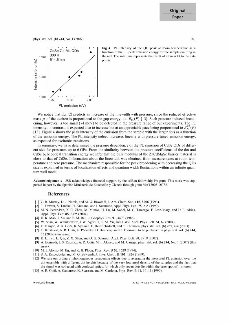
phys. stat. sol. (b) 244, No. 1 (2007) 401
www.pss-b.com © 2007 WILEY-VCH Verlag GmbH & Co. KGaA, Weinheim
Original
Paper
1.95 2.00 2.051000
1200
1400
Inte
nsity
(arb
.uni
ts)
PL emission (eV)
CdSe 7.1 ML QDs300 K514.5 nm
We notice that Eq. (2) predicts an increase of the linewidth with pressure, since the reduced effective
mass µ of the exciton is proportional to the gap energy, i.e. PL( )E P [13]. Such pressure-induced broad-
ening, however, is too small ( 1ª meV) to be detected in the pressure range of our experiments. The PL
intensity, in contrast, is expected also to increase but at an appreciable pace being proportional to 3/2
PL( )E P
[13]. Figure 4 shows the peak intensity of the emission from the sample with the larger dots as a function
of the emission energy. The PL intensity indeed increases linearly with pressure-tuned emission energy,
as expected for excitonic transitions.
In summary, we have determined the pressure dependence of the PL emission of CdSe QDs of differ-
ent size for pressures up to 6 GPa. From the similarity between the pressure coefficients of the dot and
CdSe bulk optical transition energy we infer that the bulk modulus of the ZnCdMgSe barrier material is
close to that of CdSe. Information about the linewidth was obtained from measurements at room tem-
perature and zero pressure. The mechanism responsible for the peak broadening with decreasing the QDs
size is explained in terms of localization effects and quantum width fluctuations within an infinite quan-
tum well model.
Acknowledgements JSR acknowledges financial support by the AlBan fellowship Program. This work was sup-
ported in part by the Spanish Ministerio de Educación y Ciencia through grant MAT2003-00738.
References
[1] C. B. Murray, D. J. Norris, and M. G. Bawendi, J. Am. Chem. Soc. 115, 8706 (1993).
[2] T. Tawara, S. Tanaka, H. Kumano, and I. Suemune, Appl. Phys. Lett. 75, 235 (1999).
[3] M. N. Perez-Paz, X. C. Zhou, M. Munoz, H. Lu, M. Sohel, M. C. Tamargo, F. Jean-Mary, and D. L. Akins,
Appl. Phys. Lett. 85, 6395 (2004).
[4] H. K. Mao, J. Xu, and P. M. Bell, J. Geophys. Res. 91, 4673 (1986).
[5] W. Shan, W. Walukiewicz, J. W. Ager III, K. M. Yu, and J. Wu, Appl. Phys. Lett. 84, 67 (2004).
[6] F. Manjón, A. R. Goñi, K. Syassen, F. Heinrichsdorff, and C. Thomsen, phys. stat. sol. (b) 235, 496 (2003).
[7] C. Kristukat, A. R. Goñi, K. Pötschke, D. Bimberg, and C. Thomsen, to be published in phys. stat. sol. (b) 244,
53 (2007) (this issue).
[8] K. L. Teo, L. Qin, Z. X. Shen, and O. G. Schmidt, Appl. Phys. Lett. 80, 2919 (2002).
[9] A. Bernardi, J. S. Reparaz, A. R. Goñi, M. I. Alonso, and M. Garriga, phys. stat. sol. (b) 244, No. 1 (2007) (this
issue).
[10] M. I. Alonso, M. Ilg, and K. H. Ploog, Phys. Rev. B 50, 1628 (1994).
[11] S. A. Empedocles and M. G. Bawendi, J. Phys. Chem. B 103, 1826 (1999).
[12] We rule out ordinary inhomogeneous broadening effects due to averaging the measured PL emission over the
dot ensemble with different dot heights because of the very low areal density of the samples and the fact that
the signal was collected with confocal optics, for which only seven dots lie within the laser spot of 1 micron.
[13] A. R. Goñi, A. Cantarero, K. Syassen, and M. Cardona, Phys. Rev. B 41, 10111 (1990).
Fig. 4 PL intensity of the QD peak at room temperature as a
function of the PL peak emission energy for the sample emitting in
the red. The solid line represents the result of a linear fit to the data
points.


3.3.3 Conclusions
CdSe/ZnCdMgSe dots were studied by combining Raman spectroscopy withhigh pressure measurements. This system turns out to be of particular inter-est due its high degree of reproducibility concerning its growth mechanism.Different built-in strain for dots with different height were found and itscontribution to the bandgap tuning resulted in about 18%. Interdiffusionof Mg from the barrier into the QDs was observed in resonant conditions,which were achieved using high pressure. Finally, no differences in the elasticproperties of dots with different sizes were observed from the high pressuremeasurements.


Bibliography
[1] M. N. Perez-Paz, X. C. Zhou, M. Munoz, H. Lu, M. Sohel, M. C. Tamargo,F. Jean-Mary, and D. L. Akins, Appl. Phys. Lett. 85, 6395 (2004).
[2] C. B. Murray, D. J. Norris, and M. G. Bawendi, J. Am. Chem. Soc. 115,8706 (1993).
[3] Y. H. Cho, B. J. Kwon, J. Barjon, J. Brault, B. Daudin, H. Mariette,and L. S. Dang, Appl. Phys. Lett. 81, 4934 (2002).
[4] T. Tawara, S. Tanaka, H. Kumano, and I. Suemune, Appl. Phys. Lett.75, 235 (1999).
[5] F. Flack, V. Nikitin, P. A. Crowell, J. Shi, J. Levy, N. Samarth, and D.D. Awschalom, Phys. Rev. B 54, R17312 (1996).
[6] M. Munoz, S. Guo, X. Zhou, M. C. Tamargo, Y. S. Huang, C. Trallero-Giner, and A. H. Rodrıguez, Appl. Phys. Lett. 83, 4399 (2003).
[7] K. Arai, A. Ohtake, T. Hanada, S. Miwa, T. Yasuda, and T. Yao, ThinSolid Films 357, 1 (1999).
[8] V. S. Bagaev, V. V. Zaitsev, E. E. Onishchenko, and Yu. G. Sadofyev, J.Cryst. Growth 214/215, 250 (2000).
[9] T. Yao, M. Fujimoto, S. K. Chang, and H. Tanino, J. Cryst. Growth 823,111 (1991).
67

68

Chapter 4
Complementary Articles
69


Site-controlled growth of Ge nanostructures on Si„100… via pulsed laserdeposition nanostenciling
C. V. CojocaruINRS—Énergie, Matériaux et Télécommunications, Université du Québec, 1650 Boul. Lionel-Boulet,Varennes, Quebec J3X 1S2, Canada
A. Bernardi, J. S. Reparaz, and M. I. AlonsoInstitut de Ciència de Materials de Barcelona-CSIC, Esfera UAB, 08193 Bellaterra, Spain
J. M. MacLeod, C. Harnagea, and F. Roseia
INRS—Énergie, Matériaux et Télécommunications, Université du Québec, 1650 Boul. Lionel-Boulet,Varennes, Quebec J3X 1S2, Canada
Received 12 July 2007; accepted 20 August 2007; published online 14 September 2007
The authors combine nanostenciling and pulsed laser deposition to pattern germanium Genanostructures into desired architectures. They have analyzed the evolution of the Ge morphologywith coverage. Following the formation of a wetting layer within each area defined by the stencil’sapertures, Ge growth becomes three dimensional and the size and number of Ge nanocrystals evolvewith coverage. Micro-Raman spectroscopy shows that the deposits are crystalline and epitaxial. Thisapproach is promising for the parallel patterning of semiconductor nanostructures for optoelectronicapplications. © 2007 American Institute of Physics. DOI: 10.1063/1.2783473
The growth of germanium Ge thin films and structureson silicon Si surfaces has been the subject of extensivestudy due to the prospective device applications1,2 and thefundamental research importance vis-à-vis the understandingof growth processes.3–7 In the quest to expand integratedsilicon technology, in particular, to applications in optoelec-tronics, Ge/Si nanoheterostructures8 with engineered bandstructures have come under intense investigation as impor-tant candidates for light-emitting quantum dot QD baseddevices.
Abundant research efforts have been dedicated to theexploration of “dotlike” structures obtained via the Stranski-Krastanov SK growth mode, which comprises the forma-tion of a wetting layer WL followed by three-dimensionalisland “dot” formation that relaxes the strain induced by the4.2% lattice mismatch between Ge and Si. To control thesize, shape, and density, but mostly the spatial positioning ofGe dots, many strategies including combinations oflithography-based top down and spontaneous self-organization approaches bottom up have been pursued.9–14
Much work has focused on the assisted organization of Gedots grown on prepatterned Si or SiO2 substrates either bychemical vapor deposition15,16 CVD or molecular beam ep-itaxy MBE.17–19
While CVD and MBE have been extensively used,pulsed laser deposition PLD emerged just recently20 as aversatile tool to study the structural21 and functional22 prop-erties of self-assembled Ge QDs on silicon substrates. Awell-established technique developed mainly to grow high-quality epitaxial films of complex materials,23 PLD offersadditionally the possibility of fine tuning and controllingdeposition parameters rather easily in the case of elementalmaterials. We previously investigated a promising unconven-tional patterning approach based on direct, selective PLD offunctional materials at room temperature through solid-state,reusable nanostencils. This strategy leads to the organization
of nanostructures without any pre patterning or complemen-tary invasive process prior applied to the substrates.24
In this letter we describe the patterning of Ge/Si semi-conductor heterostructures via PLD nanostenciling at hightemperature 600 °C. The intent of this approach is two-fold: first, to investigate the kinetic processes of PLD of Genanodots and ultimately to compare it with more studiedprocesses such as MBE or CVD, and, second, to demonstratea flexible approach to gain control over the positioning ofordered arrays of nanostructures with potential applicationsin device engineering.
To achieve precise positioning of Ge on Si100, weused nanostencils with hexagonal arrays of circular aperturesopened in freestanding, low-stress SiN membranes.25 Theseminiature shadow masks were mechanically clamped ontothe substrate and the substrate-stencil assembly mounted infront of a rotating Ge solid target 99% purity Fig. 1a.Prior to deposition, Si100 substrates n type, Sb doped re-sistivity of 0.015 cm were cleaned in ultrasound solventbaths. The native oxide layer was chemically removed in a5% HF solution. Ge deposition was performed in highvacuum 10−5 mbar, using a GSI Lumonics KrF excimerlaser =248 nm, =15.4 ns at a repetition rate of 10 Hzand laser fluence on the target of 4 J /cm2. The substratetemperature was set at 600 °C and the same stencil was usedin consecutive depositions.26
Swift fabrication of ordered arrays of Ge structures wasachieved in a single deposition step Fig. 1b. In the initialstages of growth up to 250 laser ablation pulses orderedarrays of Ge structures are formed as flat circular mounds,350 nm in diameter and with a 700 nm periodicity Fig.1c, i.e., the replica of the design defined by the sieve’sapertures. In Fig. 2, scanning electron microscopy SEMmicrographs for four samples illustrate the patterned Ge is-lands obtained on Si100 by varying the number of laserpulses between 250 and 1500 with an estimated rate of0.28 Å/pulse. SEM micrographs show that with increasingGe thickness, the shapes of the obtained structures evolveaElectronic mail: [email protected]
APPLIED PHYSICS LETTERS 91, 113112 2007
0003-6951/2007/9111/113112/3/$23.00 © 2007 American Institute of Physics91, 113112-1Downloaded 20 Sep 2007 to 158.109.18.63. Redistribution subject to AIP license or copyright, see http://apl.aip.org/apl/copyright.jsp

from the flat “two-dimensional 2D-mound” type Fig. 2ato three-dimensional 3D nanocrystalline agglomerations10–100 nm in lateral size formed on top of these moundsFig. 2b, undergoing further a transition to a “coffee-bean-like” grained structure Fig. 2c, and finally coalescing intosingle nanocrystals Fig. 2d. Atomic force microscopyAFM and SEM images from Figs. 1 and 2 show that allislands are perfectly separated and well defined. The lateralextent of the deposits is always restricted to the range of theaperture areas defined in the stencil.
Micro-Raman spectroscopy was used to provide a struc-tural characterization of the Ge clusters. The optical mea-
surements were carried out by probing the patterned areawith the 514.5 nm line of an Ar+ ion laser focused with aspot size of about 1 m, i.e., each Raman spectrum Fig. 3is collected from the region of two to three apertures. Thespectral position and shape of the Ge–Ge phonon mode re-veal that the Ge clusters are crystalline, and the absence ofthe Si–Ge phonon band around 400 cm−1 inset in Fig. 3clearly indicates that there is no Si intermixing. Further, theGe–Ge phonon peak becomes more intense with increased
FIG. 1. Color online Experimental setup used for stencil deposition and further characterization of Ge ordered arrays: a schematic drawing of thePLD-based Ge direct patterning process achieved at high temperature through SiN stencils attached to the Si100 substrates; b SEM micrograph showingan AFM tip scanning across the Ge patterned area in a JEOL-4500 UHV AFM-STM-SEM microscope. The inset shows a detail of a perforated freestandingSiN membrane built in the stencil chip; c AFM topography and Ge mound height profile obtained for 250 pulses deposited at 600 °C using a stencil withthe architecture shown in the inset b.
FIG. 2. Coverage dependence of Ge morphology: SEM micrographs show-ing ordered Ge nanostructures replicated on Si100 by PLD at 600 °C, fora 250, b 750, c 1250, and d 1500 laser pulses with a fluence of4 J /cm2, for a target-substrate distance of 6.5 cm.
FIG. 3. Color online Raman spectra acquired by probing the Ge patternedareas with the 514.5 nm line of an Ar+ ion laser. The absence of the Si–Gephonon band around 400 cm−1 see inset indicates no trace of Siintermixing.
113112-2 Cojocaru et al. Appl. Phys. Lett. 91, 113112 2007
Downloaded 20 Sep 2007 to 158.109.18.63. Redistribution subject to AIP license or copyright, see http://apl.aip.org/apl/copyright.jsp
Ge coverage. Spectra recorded after the initial stages ofgrowth exhibit a blueshifted Ge–Ge phonon frequency303 cm−1 attributed to compressive strain −1% atthe island-substrate interface.27 The strain is progressivelyrelieved for taller clusters i.e., higher Ge coverage whosephonon frequency approaches the value expected for bulk Ge300.8 cm−1. The presence of built-in strain suggests thatthe Ge nanostructures match the Si substrate lattice. In fact,they retain the substrate crystallographic orientation, as con-firmed by the phonon selection rules in polarized Ramanmeasurements not shown here.
The 2D mounds are reminiscent of the thin WL whichnormally precedes islanding in classical SK growth. AFMtopographies indicate that the 2D mounds grow to a maxi-mum height of 6–7 nm, roughly ten times thicker than thecritical value for a conventional Ge WL.28 The anomalouscritical thickness for the onset of 3D nucleation can be ex-plained by invoking the finite size of the deposited areas: the2D mounds, acting as a WL, relieve strain at their periphery,delaying the strain-induced 3D nucleation of structures.Similar phenomenology was discussed in the case of self-assembling of Ge on lithography-patterned windows openedin ultrathin silicon oxide layers.29
The dots that initially nucleate on top of the 2D moundsFig. 2b are round shaped and their aspect ratios definedas the dot’s height divided by the square root of the basearea range from 0.16 to 0.20. These dots are reminiscentof the dome-shaped islands observed in Ge/Si001heteroepitaxy.30 The average aspect ratio of the dots in-creases with coverage to allow for more efficient strain re-laxation. Above 500 pulses, we observe a shape transitionfrom rounded to “coffee-bean” dots Fig. 2c. At this stageof growth, we detect both coalescence of grains and the for-mation of a depletion region at the center of the underlying2D mounds, where we expect higher elastic compression.Finally, at higher Ge coverage above 1000 ablation pulses,the depletion region disappears and is replaced by a singlerounded cluster.
The number of Ge dots is of the order of tens per aper-ture for the samples deposited from 250 up to 500 pulses.For samples deposited up to 1000 pulses, the dots are largerand less numerous e.g., three to five dots/aperture as shownin Fig. 2b. This implies a feasible control over the numberof dots per nominal location and thus their density in thewhole patterned area.31
In summary, we showed that combining nanostencilingwith PLD provides a flexible approach to grow and patterncrystalline Ge/Si nanostructures. The location of the Geclusters is entirely controlled by the pattern of the nanosten-cil, and the density and physical dimensions of the dots canbe further adjusted by varying the deposition parameters.The morphological evolution of the structures with coveragefollows a modified Stranski-Krastanov growth mode due tothe finite size of the WL in each aperture location. Ramanspectroscopy indicates that the nanostructures are crystallineGe and that they follow the substrate’s crystallographic ori-entation. In future work we will establish a correlation be-tween the deposition parameters such as laser fluence, sub-strate orientation and temperature, and the Ge dots’ densityper deposited site.
The authors acknowledge financial support from theCanada Foundation for Innovation, and NSERC of Canada.F.R. is grateful to FQRNT and the Canada Research Chairsprogram for salary support. A.B. acknowledges a FPI fellow-ship. J.S.R. acknowledges financial support from the AlBanfellowship Program. This work was supported in part by theSpanish Ministerio de Educación y Ciencia through GrantNo. MAT2006-02680.
1J. Konle, H. Presting, H. Kibbel, K. Thonke, and R. Sauer, Solid-StateElectron. 45, 1921 2001.
2D. L. Harame, S. J. Koester, G. Freeman, P. Cottrel, K. Rim, G. Dehlinger,D. Ahlgren, J. S. Dunn, D. Greenberg, A. Joseph, F. Anderson, J.-S. Rieh,S. A. S. T. Onge, D. Coolbaugh, V. Ramachandran, J. D. Cressler, and S.Subbanna, Appl. Surf. Sci. 224, 9 2004.
3D. J. Eaglesham and M. Cerullo, Phys. Rev. Lett. 64, 1943 1990.4G. Medeiros-Ribeiro, A. M. Bratkovski, T. I. Kamins, D. A. A. Ohlberg,and R. S. Williams, Science 279, 353 1998.
5F. M. Ross, J. Tersoff, and R. M. Tromp, Phys. Rev. Lett. 80, 984 1998.6J. Stangl, V. Holý, and G. Bauer, Rev. Mod. Phys. 76, 725 2004.7F. Ratto, G. Costantini, A. Rastelli, O. G. Schmidt, K. Kern, and F. Rosei,J. Exp. Nanosci. 1, 279 2006.
8J. M. Baribeau, X. Wu, N. L. Rowell, and D. J. Lockwood, J. Phys.:Condens. Matter 18, R139 2006.
9J. R. Heath, R. S. Williams, J. J. Shiang, S. J. Wind, J. Chu, C. D’Emic, W.Chen, C. L. Stanis, and J. J. Bucchignano, J. Phys. Chem. 100, 31441996.
10T. I. Kamins and R. S. Williams, Appl. Phys. Lett. 71, 1201 1997.11E. S. Kim, N. Usami, and Y. Shiraki, Appl. Phys. Lett. 72, 1617 1998.12G. Capellini, M. de Seta, C. Spinella, and F. Evangelisti, Appl. Phys. Lett.
82, 1772 2003.13A. Karmous, A. Cuenat, A. Ronda, I. Berbezier, S. Atha, and R. Hull,
Appl. Phys. Lett. 85, 6401 2004.14A. Bernardi, M. I. Alonso, A. R. Goñi, J. O. Ossó, and M. Garriga, Appl.
Phys. Lett. 89, 101921 2006.15T. I. Kamins, D. A. A. Ohlberg, R. S. Williams, W. Zhang, and S. Y. Chou,
Appl. Phys. Lett. 74, 1773 1999.16L. Vescan, Mater. Sci. Eng., A 302, 6 2001.17O. G. Schmidt, N. Y. Jin-Phillipp, C. Lange, U. Denker, K. Eberl, R.
Schreiner, H. Grabeldinger, and H. Schweizer, Appl. Phys. Lett. 77, 41392000.
18G. Jin, J. L. Liu, and K. L. Wang, Appl. Phys. Lett. 76, 3591 2000.19Z. Zhong, A. Halilovic, M. Muhlberger, F. Schäffler, and G. Bauer, J.
Appl. Phys. 93, 6258 2003.20B. Shin, J. P. Leonard, J. W. McCamy, and M. J. Aziz, Appl. Phys. Lett.
87, 181916 2005.21M. S. Hegazy and H. E. Elsayed-Ali, J. Appl. Phys. 99, 054308 2006.22X. Ma, Z. Yan, B. Yuan, and B. Li, Nanotechnology 16, 832 2005.23D. B. Chrisey and G. K. Hubler, Pulsed Laser Deposition of Thin Films
Wiley, New York, 1994.24C. V. Cojocaru, C. Harnagea, A. Pignolet, and F. Rosei, IEEE Trans.
Nanotechnol. 5, 470 2006.25The stencil chip has 14 freestanding membranes, 2 mm in length and
100 m in width; nominal diameter of the circular apertures is 350 nmand the pitch 700 nm; stencils fabricated at Aquamarijn Filtration, TheNetherlands.
26Samples were prepared with various Ge thicknesses coverages. In PLD,the deposited film thickness is controlled by varying the number of laserpulses for a certain target-substrate distance provided that desorption fromthe substrate is negligible.
27A. Bernardi, J. O. Ossó, M. I. Alonso, A. R. Goñi, and M. Garriga,Nanotechnology 17, 2602 2006.
28Typically 0.4–0.6-nm-thick for Ge on Si001; Y.-W. Mo, D. E. Savage,B. S. Swartzentruber, and M. G. Lagally, Phys. Rev. Lett. 65, 10201990.
29L. Vescan, T. Stoica, B. Holländer, A. Nassiopoulou, A. Olzierski, I. Rap-tis, and E. Sutter, Appl. Phys. Lett. 82, 3517 2003.
30A. Rastelli, M. Stoffel, J. Tersoff, G. S. Kar, and O. G. Schmidt, Phys.Rev. Lett. 95, 026103 2005.
31For any given set of deposition parameters, the sizes of the dots are fairlynarrowly distributed. Their density can be further tuned by using stencilswith smaller or larger apertures and varying PLD parameters.
113112-3 Cojocaru et al. Appl. Phys. Lett. 91, 113112 2007
Downloaded 20 Sep 2007 to 158.109.18.63. Redistribution subject to AIP license or copyright, see http://apl.aip.org/apl/copyright.jsp


IOP PUBLISHING NANOTECHNOLOGY
Nanotechnology 18 (2007) 475401 (7pp) doi:10.1088/0957-4484/18/47/475401
Evolution of strain and compositionduring growth and capping of Gequantum dots with different morphologiesA Bernardi, M I Alonso, J S Reparaz, A R Goni1, P D Lacharmoise,J O Osso2 and M Garriga
Institut de Ciencia de Materials de Barcelona-CSIC, Esfera UAB, 08193 Bellaterra, Spain
E-mail: [email protected]
Received 13 July 2007, in final form 26 September 2007Published 17 October 2007Online at stacks.iop.org/Nano/18/475401
AbstractWe follow the growth of islands with different shapes by monitoring thestrain relaxation by reflection high energy electron diffraction (RHEED).Comparing a bimodal ensemble of pyramids and domes with a monomodaldistribution of C-induced domes, we observe different relaxation pathwaysand a growth mode change from Stranski–Krastanow to Volmer–Weber. Wealso study the changes induced by the capping process with Si. Small strainsin thin cap layers are revealed by spectroscopic ellipsometry. Ramanspectroscopy is employed to probe the built-in strain and silicon intermixingin different types of islands, evidencing that smaller islands are enriched in Siand effectively recompressed, whereas bigger relaxed dots remainsubstantially unaffected.
(Some figures in this article are in colour only in the electronic version)
1. Introduction
The challenge of turning nanostructures like self-assembledquantum dots (QDs) into future nanoscale devices criticallydepends on the possibility to tailor the island shape, sizedistribution, composition and strain status [1–3]. In standardGe/Si heteroepitaxy, ‘anomalous’ coarsening [4] and Si–Ge intermixing [5] compete as ways for elastic strainrelaxation. The typical result is a broad dot-size distributionof coherent islands having different shapes [6–8] (shallowpyramids and steeper domes or barns). For large islands,called superdomes, there is a competition between elasticand plastic relaxation, which depends on the substratetemperature [9–11]. Classifications of island shapes and usualrelaxation mechanisms are summarized in [8]. The populationof domes and pyramids in an ensemble of islands is relatedto the total Ge coverage and the growth temperature [12],with bigger pyramids transforming into domes when a criticalvolume is reached. During annealing, the morphology ofstrained islands eventually oscillates [8, 13] between shallow
1 ICREA Research Professor.2 Present address: MATGAS 2000 AIE, 08193 Bellaterra, Spain.
and steeper shapes [14] so that the final dot topography is ratherunpredictable. The drawback of the coexistence of islands withdifferent shapes is that they are not only inhomogeneous insize but they also exhibit different composition [15] and elasticproperties.
To achieve better dot uniformity there are differentpossible strategies. It is possible to remove large clustersand keep small pyramids by growth interruption and hightemperature annealing [16]. In the Ge/Si system pyramidsare strongly intermixed and dome-shaped islands with largeraspect ratios and Ge-rich compositions are preferred. In orderto obtain small domes, a simple bottom-up strategy involvessurface modification by addition of impurities [17–21], whichaffect the kinetics and alter the energetics of nucleation.Deposition of carbon during the process of QD growth enablesa dramatic decrease of the diffusion length of adatoms anda modification of the strain field of the surface. Carbonpromotes the growth of domes even at very low Ge coverageand in a wide temperature range [20, 22] without thecoexistence of pyramids or hut clusters. The peculiar interplayof chemical interactions between Si, Ge and C and theresulting local enhancement of strain are responsible for
0957-4484/07/475401+07$30.00 1 © 2007 IOP Publishing Ltd Printed in the UK

Nanotechnology 18 (2007) 475401 A Bernardi et al
relevant changes in the growth mechanism. In addition tobetter sample homogeneity, size-reduced domes are attractivefor the conception of quantum optoelectronic devices [1].However, we point out that radiative recombination willtypically be indirect in real space (type II), suitable for instancefor photodetector operation. Type I structures suitable forstimulated emission are possible at even smaller sizes, as wasdemonstrated from submonolayer Ge QDs [23].
In the present work we describe an experimentallyobserved growth mode change from Stranski–Krastanow (SK)in the absence of C to Volmer–Weber (VW) when depositingGe on a C-enriched Si substrate. The evolution of the surfacelattice parameter is followed up to large Ge coverage whereboth elastic and plastic mechanisms of relaxation are active.We also study the process of capping the islands with siliconto understand how it affects the final composition and theelastic recompression of the dots. Finally, we also focus onthe structural properties of the cap layer and obtain evidenceof the existence of compressive stress induced by local strainfields associated with carbon-rich patches.
2. Experimental details
Samples under investigation were prepared by solid-sourcemolecular beam epitaxy. After oxide desorption at 900 Cand 100 nm thick Si buffer layer deposition, the substratetemperature was set to 500 C. Subsequently, ∼0.1 monolayers(MLs) of carbon were predeposited on the Si surface froma calibrated sublimation filament. The self-assembling ofcarbon-induced quantum dots (C-QDs) was achieved byevaporation of 12 MLs of Ge. A reference sample was preparedfollowing exactly the same growth procedure as above, butomitting the step of carbon predeposition. As a result standardStranski–Krastanow quantum dots (SK QDs) were obtained.Finally, part of the surface of the samples was capped witha 10 nm thick Si layer deposited at 300 C, in order not toalter the shape of buried dots. Growth was monitored in situby reflection high energy electron diffraction (RHEED) andthe island topography was studied ex situ by atomic forcemicroscopy. In order to evaluate the composition and residualstrain, samples were characterized by optical measurements atroom temperature. Raman spectroscopy was carried out withthe 514.5 nm line of an Ar-ion laser for excitation. Lightwas focused onto the sample with a spot size of about 1 μmand a laser power of 4 mW. In order to suppress contributionsfrom second-order processes, we used the scattering geometryz(xy)z, where x , y and z are the [100], [010] and [001]crystallographic directions, respectively. The ellipsometricspectra were collected using a rotating polarizer ellipsometerin the 1.4–4.8 eV spectral range.
3. Results
3.1. Growth mode and dot topography
When comparing conventional island ensembles with C-induced QDs the first striking feature concerns the morphol-ogy. We use the same island shape denominations as thosegiven in [8]. There are two equilibrium island shapes: shal-low islands called pyramids (Ps) with 105 crystallographic
Figure 1. Topographic images of uncapped Stranski–Krastanowquantum dots (SK-QDs) (left) and carbon-induced QDs (C-QDs)(right). The grey scale indicates surface inclination (steeper facetscorrespond to darker color). Labels in figure refer to pyramids (Ps),transition domes (TDs) and domes (Ds).
planes and domes (Ds) with steeper 113 facets. The aspectratios (defined as the dot height over the square root of the basisarea) of these islands are different: pyramids have aspect ratiosmuch smaller than 0.1 and well-developed domes have valuesaround 0.2. The evolution P → D may be rather continuousand the transition islands are called transition domes (TDs),with aspect ratios around 0.15. By changing shapes, islandsrelax elastically, i.e., Ps and TDs are coherent islands. WhenTDs evolve into Ds reaching a critical size, plastic relaxationwill set in [9, 10] giving rise to larger dome-shaped dislocatedislands (superdomes).
We compare the different morphologies in figure 1. Wechoose a representation with the facet inclination as the z-scale, so that different grey-levels indicate different families ofislands. That is, lighter dots are shallow pyramids and darkerislands correspond to domes. Ordinary SK self-assemblingof Ge islands on Si (left panel) leads to a broad bimodaldistribution of pyramids and domes. Addition of carbon to thesurface, due to the enhancement of strain fields, stabilizes thedome-shaped islands [24]. In the C-QD ensemble (right panel)even the smaller islands are dome-shaped, with aspect ratiosincreasing with the dot volume, from ∼0.1 for the smaller ortransition domes to ∼0.2 for the bigger domes. It is evidentthat the use of carbon yields better island homogeneity with amuch narrower dot size distribution, although in this examplewe go beyond optimal coverage on purpose.
In order to unravel the mechanism leading to such differentdot topographies, we performed in situ RHEED experimentsduring the growth of the islands. In figure 2 we showthe evolution from the streaky pattern of an atomically flatSi(001) surface to the spotty pattern associated with the surfaceroughening and nucleation of islands. Apart from a qualitativeoverview of the growth process from RHEED images it ispossible to extract streak intensity profiles which allow us toobtain quantitative information [25] about the strain relaxationmechanism. The spacing of diffraction streaks gives therelative variation of the in-plane lattice parameter in realtime [26–28].
The measured evolution of in-plane lattice parameter isplotted in figure 3. The top panel corresponds to SK self-assembling. In this case, during the first stage of Ge deposition
2

Nanotechnology 18 (2007) 475401 A Bernardi et al
Figure 2. RHEED patterns (top panels) along a 〈110〉 azimuth of aflat (2 × 1)-reconstructed Si(001) surface and of transmissiondiffraction from 3D islands. The bottom panels show thecorresponding streak intensity profiles extracted from RHEEDimages.
we do not observe any evolution of the lattice parameter,consistent with the growth of a flat pseudomorphically strainedwetting layer (WL). After a critical coverage of 4–5 MLs thestreaky pattern starts to evolve into a spotty pattern and fromthe streak spacing variation we infer a progressive increase ofthe lattice parameter, which indicates a strain relief associatedwith the transition from 2D growth to nucleation of 3D clusters.These observations are consistent with the expected Stranski–Krastanow (SK) growth mode. Moreover, from our data wecan recognize clearly two stages of strain relaxation. A firstplateau around the value a‖
aSi 1% can be attributed to the
nucleation and growth of shallow pyramids, and progressiverelaxation up to 2% corresponds to their shape transition intosteeper domes [7, 12, 14]. After about 10 MLs of Ge coveragewe observe a quicker relaxation, almost reaching the latticemismatch value for Ge bulk (∼4%). This can be associatedwith a more efficient plastic strain relief leading to dislocateddomes (also called superdomes). At the final coverage of12 MLs all these islands coexist.
If we now consider the strain relaxation pathway for C-QDs shown in the bottom panel of figure 3, we observe thatthe lattice parameter starts to evolve from the very early stagesof Ge deposition, indicating that 3D relaxation occurs withoutthe formation of a flat strained WL. This strain relaxationdynamics confirms that the presence of C on the surfaceinduces a change of growth mode from Stranski–Krastanowto Volmer–Weber (VW), as previously demonstrated by otherRHEED experiments [29, 30] (qualitative study of the streaky–spotty transition) and scanning tunneling microscopy [31].In our present quantitative RHEED data analysis of C-QDsgrowth we cannot appreciate sharply differentiated stagesof strain relaxation, suggesting that there is no clear shapetransition. This observation is consistent with the measuredfinal AFM topography revealing dot homogeneity, withoutthe presence of islands with different shapes. However, thequick lattice relaxation between 6–8 MLs is likely to involvedislocations.
Ge deposited (MLs)
Figure 3. In-plane lattice parameter relaxation associated with thenucleation of 3D islands obtained from RHEED intensity profiles.The vertical arrow indicates the point where dot nucleation for theconventional Stranski–Krastanow islands sets in (top panel).
3.2. Recompression of capped islands and Si intermixing
We now turn to discuss the effects of capping with Si,which changes the strain status of the dots [32, 33] andcomposition [34–36]. Knowledge of the complex strainfield generated inside and outside the dots is determinantfor predicting the properties of the nanostructures and forengineering the process of piling up a multistack of verticallycorrelated islands [2, 37, 38]. During capping, the additionalstrain is partially relieved by Si intermixing into the islands, sothat the composition of the island is expected to change towardsa Si enrichment [34]. Notice that capping is done here atsubstrate temperature of 300 C, which we checked preservesthe island shapes.
Raman spectroscopy is a surface sensitive techniqueuseful to extract information about both composition andstrain inside the QDs [10, 24, 35, 36, 39–41]. In figure 4(a)we show the Raman spectra for the investigated samples,where the dominant feature is the Ge–Ge phonon band near300 cm−1. We always observe that the uncapped samplesare characterized by weaker peak intensities, possibly due topartial oxidation of the dots and to the presence of surfacestates that reduce the electronic lifetimes, affecting the resonantenhancement of the Raman intensity. In contrast, in the cappedsamples, larger Raman intensity close to resonance is possiblein the absence of surface states [32]. Moreover, a Si–Geband at ∼400 cm−1, which was almost absent for uncappedsamples (see inset to figure 4(a)), is apparent in the spectraof the capped samples. The relative intensity between Ge–Ge and Si–Ge phonon bands [42, 43] gives at a first glanceinformation on the average composition: uncapped islands arealmost pure Ge (xGe > 90%), whereas capped islands havea composition ranging from xGe ∼ 80% (for SK QDs) toxGe ∼ 85% (for C-QDs). The Si intermixing at relativelylow temperature is driven by surface diffusion rather than bybulk processes [5, 44, 45], so the reduced adatom mobilityassociated with the presence of carbon may be the reason whycapped C-QDs remain slightly Ge richer.
3

Nanotechnology 18 (2007) 475401 A Bernardi et al
Figure 4. Raman spectra of C-induced and SK QDs for capped anduncapped samples (all with 12 MLs Ge). The inset shows the Si–Gephonon mode associated with the Si intermixing during the cappingprocess. The bottom panel represents a close-up of the spectra in theregion of the Ge–Ge phonon mode. The spectra can be fitted withtwo asymmetric Gaussians (shown in the figure). The vertical lineindicates the Ge–Ge phonon frequency for bulk Ge.
By fitting the peak positions of the phonon bands itis possible to obtain further insight into the nanostructurecomposition and especially in the strain status. The presence ofsome dislocated islands does not affect the subsequent analysis,which is completely general. Qualitatively, a red-shift of theGe–Ge peak is associated with Si enrichment, and a blue-shiftis indicative of compressive strain. In figure 4(b) the main Ge–Ge peak is shown with greater detail. The peak position forthe Ge–Ge band of uncapped islands (∼301.3 cm−1) is quiteclose to the frequency expected for relaxed Ge (300.8 cm−1),whereas capped samples are characterized by a blue-shift ofthe Ge–Ge peak ascribed to the partial recompression of thedots. From figure 4(b) it is remarkable that after cappingwe are able to resolve two clear contributions to the phononmode, which can be deconvoluted by fitting two Gaussianterms, giving a low frequency peak at ωGe−Ge 305 cm−1
and a high frequency peak at ωGe−Ge 310 cm−1. Similar
features observed for nominally monomodal ensembles of dotswere recently interpreted as the fingerprints stemming froman intermixed shell and a Ge-rich core, respectively [41].This core/shell model does not hold for our experiment sincethe low frequency peak (associated with intermixing duringencapsulation of islands) is already present for uncapped dots.Considering the topography of the present samples, we ratherascribe the two contributions to two different families ofislands: the high frequency mode is associated with smallercompressed pyramids or transition domes, in the case of the C-QDs, whereas the low frequency peak is mainly related to thebigger relaxed domes with dislocations. Notice in figure 4(a)that the two spectral contributions to the Ge–Ge band can berelated to those observed in the Si–Ge band spectral range,namely a lower frequency broad band at ∼390 cm−1 and ahigher frequency peak at ∼420 cm−1. The observation oftwo Ge–Ge modes and their two Si–Ge counterparts allowsus to solve for values of composition and strain, as detailedbelow. The only combination that makes sense is to pair bothlower frequency peaks (305 and 390 cm−1) and both higherfrequency peaks (310 and 420 cm−1). Taking into account theexperimental composition dependence for both the Ge–Ge andSi–Ge LO phonon bands [46], we obtain the following systemof two equations where the unknowns are the composition x inSi1−x Gex and strain ε‖ [24, 10]:
ωGe−Ge = 284 + 5x + 12x2 + bGe−Geε‖, (1)
ωSi−Ge = 400+29x −95x2+213x3−170x4 +bSi−Geε‖, (2)
provided the strain-shift coefficients b of the last terms ofequations (1), (2) are known. The generalized expression is
b = ω(x)(−K11α/2 + K12). (3)
In equation (3), Ki j are the deformation potentials andα = −ε⊥/ε‖ describes the strain field inside the dots.It is generally assumed that the Ge islands are biaxiallystrained [2] (α 0.75) like a flat pseudomorphic layer, butthis approximation might be inaccurate at least for capped dotswith steeper facets (domes) that should tend to an hydrostaticstrain field (α = −1) [33]. Typical experimental values forbGe−Ge of Si1−x Gex alloys and Ge quantum dots reported inthe literature [40, 42, 43, 47] show considerable dispersion,ranging from −400 to −1000 cm−1, remarkably matching thevalues that can be obtained from equation (3), if we considerthe limiting cases of biaxial and hydrostatic strain (assumingthat the deformation potentials of Ge are K11 = −1.57 andK12 = −2.07)Note 3. Since the values of b directly affect theobtained ε‖, we conclude that the main source of uncertaintyin determining the strain in the dots comes from the lack ofconsensus in choosing the proper elastic model to describe acompressed island. Therefore, in table 1 we report two resultsassuming both limiting cases of biaxial and hydrostatic strainfields.
The dot compositions obtained from this detailed analysisand reported in table 1 are compatible with the averagecompositions determined above from the peak intensity ratiobetween the Ge–Ge and Si–Ge modes. Uncapped samplesconsist of Ge-rich islands (∼90%) and are almost fully relaxed.
3 Our measurement, unpublished.
4

Nanotechnology 18 (2007) 475401 A Bernardi et al
Figure 5. Second derivative with respect to energy of the dielectricfunction (imaginary and real parts) of the Si cap layer as obtainedfrom the ellipsometry spectra. Arrows represent the fitted energiesfor the electronic transition E1. The vertical line shows the E1 energyfor unstrained silicon, and a blue-shift (red-shift) corresponds tocompressive (tensile) strain.
Table 1. Composition and strain obtained from the peak positions ofthe Ge–Ge and Si–Ge phonon modes. For capped samples the resultsrefer to both the high and low frequency contributions to the Ramanspectra. We calculate strain assuming both limiting cases of biaxialand hydrostatic strain. In the last column we report as a reference themaximum strain given by the lattice mismatch for each composition.
xGe (%)
εbiaxial‖
(%)ε
hydrostatic‖
(%) εmax‖ (%)
SK QDs 92 ± 2 −1.0 −0.4 −3.7SK QDs + cap 77 ± 15 −3.0 −1.6 −3.0
89 ± 3 −1.1 −0.5 −3.5C-QDs 92 ± 2 −0.8 −0.3 −3.7C-QDs + cap 82 ± 15 −3.2 −1.9 −3.2
94 ± 2 −1.3 −0.6 −3.8
After capping, there are two distinct regions showing not onlydifferent intermixing but also different strain. This meansthat some of the islands, presumably the smaller dots, become∼10% richer in silicon and are strongly compressed. In fact,accepting that strain in small islands is well described by abiaxial model [33], then they turn out to be fully compressedupon capping. In contrast, the family of bigger islands remainsGe rich and only slightly recompressed by the cap layer.Results obtained by Raman spectroscopy confirm that theintermixing process during capping is strain-driven and affectsmostly the smaller (Ps and TDs) coherent islands.
3.3. Structural properties of the cap layer
Characterization by spectroscopic ellipsometry, complement-ing the results from RHEED and Raman, is useful in under-standing the inhomogeneity of the strain field of the cap layerin the regions above the islands and in between them [37, 48].
Spectroscopic ellipsometry represents a powerful comple-mentary diagnostic tool allowing one, in particular, to probethe thin layer of silicon covering the islands. From the ellipso-metric measurement we determine the thickness of deposited
Figure 6. Sketch of the inhomogeneous strain field associated with aC-QD. Relaxed islands induce a tensile strain in the thin cap layer.Nevertheless, the presence of C-rich patches introduces compressivestrain in the region of cap layer surrounding the islands.
cap layer and extract its dielectric function with an accuratefitting procedure and inversion algorithm, as discussed else-where [10]. By fitting the second derivative spectra of the caplayer dielectric function, we obtain the energy of the E1 elec-tronic transition [49], indicated by vertical arrows in figure 5.In the reference sample grown without carbon predepositionthe E1 transition is found to be slightly red-shifted comparedto bulk Si, indicating the presence of average tensile strain inthe cap layer induced by the Ge dots (see the sketch in figure 6).Surprisingly, the E1 energy for the cap layer deposited on theC-QD sample is blue-shifted, thus reflecting the presence ofaverage compressive strain, in spite of the presence of buriedGe islands which are expected to induce local tensile strain inthe overgrown silicon. The structural information obtained byellipsometry is an areal average of all the sample surface and incontrast to RHEED and Raman measurements does not providelocal information related only to the dots. The results indicatethat the silicon layer that grows on the C-alloyed surface whichsurrounds the islands must be compressively strained.
4. Discussion
By using complementary surface science tools we were able tostudy different aspects of the growth of strained Ge/Si islands.RHEED was used to in situ monitor the evolution of the in-plane lattice parameter, allowing us to determine the set inof strain relaxation due to nucleation of 3D clusters. In theabsence of C, we observed the formation of a flat 2D layer(WL), taking place before the gain in elastic energy becomesdominant over the energetic term associated with the increaseof surface (SK growth). In this case, the first stage of islandgrowth accounts for the relaxation of less than 50% of thelattice mismatch and it can be attributed to the nucleation ofsmall and shallow pyramids. When the islands get bigger,they transform into domes or dislocated Ge clusters that canefficiently relax the strain, so that after 10 MLs of coverage wealready measure a lattice parameter approaching the value ofbulk Ge.
The strain-relaxation pathway changes quite dramaticallywhen carbon is used to engineer the dot topography. In thiscase, the presence of carbon-rich patches and the repulsiveGe–C interaction prevent the formation of a WL, i.e., itis energetically more convenient to increase the Ge surfacewith nucleation of 3D clusters, rather than wetting the
5
Nanotechnology 18 (2007) 475401 A Bernardi et al
carbon-alloyed surface. As a result, the lattice parameterrelaxation associated with the 3D nucleation can be observedstarting from the very first stages of Ge deposition whichis experimental evidence of the growth mode change fromStranski–Krastanow to Volmer–Weber. In the case of C-QDs,we do not observe two regimes of strain relaxation (shallowand steeper islands) but a continuous progressive evolution ofthe lattice parameter, and this observation is consistent with theAFM topography characterized only by dome-shaped clusters.The density of domes is exceptionally high (∼1011 cm−2)
due to reduced mobility of Ge on a roughened carbon-alloyedsurface. Surprisingly, the smaller domes have volumes muchbelow the typical threshold value expected for the pyramid-to-dome shape transition, i.e., the presence of carbon reducesdrastically the critical volume associated with the ‘anomalous’coarsening. This experimental observation can be accountedfor by the enhanced effective mismatch between the substrateand the overlayers [24], without the need to invoke differencesof the surface energy between shallower and steeper facetsrelated to the presence of carbon, since the carbon is arrangedin patches outside the islands. The reduced surface diffusionthat explains the high dot density is likely to be also responsiblefor the quenching of Si intermixing in the islands. Both islandmorphology and composition keep evolving while the growthor annealing proceeds. Intermixing dynamics is thought tobe dominated by surface rather than bulk diffusion [5, 44],especially at temperatures below 500 C. Therefore, it ispossible that in the presence of C the process of Si intermixingis kinetically limited. Then, capped C-QDs are less intermixedand retain larger strain than SK-QDs, as experimentallyobserved (see table 1). The limited intermixing as a partialstrain-reliever and the presence of local inhomogeneous strainfields are both consistent with the extreme decrease of thecritical volume for the pyramid-to-dome transition, to the pointwhere only dome-shaped clusters can be observed.
As a result of the deposition of 12 MLs of Ge, thedots completely relax their strain towards their apex, as canbe measured by RHEED probing the topmost atomic layers.Raman spectroscopy becomes a useful tool to study instead theaverage strain distribution inside the volume of the islands. Therelevant question arising when evaluating the Raman resultsis to decide which is the adequate elastic model to describethe strain status of a quantum dot. Once we have measuredthe LO phonon frequency shift associated with the latticedeformation, in order to quantify the strain, we need to knowthe relation existing between the in-plane (ε‖) and out-of-plane (ε⊥) components. A tiny shallow island is somehowsimilar to a pseudomorphic 2D layer and its strain statusis likely described by a biaxial model (i.e., the lattice iscompressed in the in-plane direction and it is free to expandin the out-of-plane direction, according to Hooke’s law). Forsteeper islands embedded in a matrix (capped dots) [32, 33],the strain status of dots can be rather described by a hydrostaticmodel (ε⊥ = ε‖). According to the results listed in table 1 theuncapped dots (both SK and C-QDs) retain only between 10%and 30% of the strain, depending on whether we consider ahydrostatic or biaxial model, respectively.
After capping with a 10 nm thick Si layer, the islandsare recompressed and we can clearly recognize in Ramanspectra features corresponding to two contributions from
portions of material with different composition and strain.The experimental piece of evidence is that we are probingregions of material with rather different structural properties;thus, it is unlikely that they refer to different portions ofthe same island. This argument leads us to ascribe thecontributions to two separate families of islands: the smallercoherent islands are fully recompressed (according to thebiaxial model) whereas the bigger relaxed domes are lessaffected by the thin cap layer [33]. Raman spectroscopyturns out to be a powerful technique capable of pointingout the presence of local structural inhomogeneities of thequantum dots, complementing the information achieved byRHEED analysis. When probing dot ensembles most of thecharacterization tools are sensitive to the 3D clusters due to thegrazing incidence geometry and shadowing (this is the case ofRHEED) or for confinement of carriers in the islands and theabsence of a signal collectable from the WL (like in Ramanspectroscopy [24, 40]). In this context, ellipsometry providesunique information on the average strain field of the silicon caplayer, which indicates a local compressive strain in the regionsbetween islands associated with the carbon-rich patches.
5. Conclusions
In summary, we have studied the strain relaxation mechanismduring self-assembling of Ge QDs, comparing the conventionalGe/Si heteroepitaxy with the carbon-engineered growth.RHEED analysis permitted us to recognize three stages ofstrain relaxation after the growth of a pseudomorphic WL,corresponding to the nucleation of pyramids, the shapetransition to domes, and dislocation formation. For thesample obtained after pre-depositing carbon on the siliconsubstrate, we found instead experimental evidence for a growthmode change from Stranski–Krastanow to Volmer–Weber. Anellipsometric study of the silicon cap layer was helpful to pointout the presence of compressive strain associated with the localstrain field in proximity of the carbon-rich patches in betweenthe islands.
The topography of the quantum dot ensembles wascorrelated to the structural properties (i.e., strain andcomposition) measured by Raman spectroscopy. In particular,the capping process put in evidence two distinct regions of thesample with different local composition and elastic properties.We interpreted our experimental results as signals coming fromtwo families of islands, i.e., smaller intermixed dots that gethighly recompressed and bigger domes only slightly affectedby the deposition of the silicon cap layer.
Optical techniques combined with RHEED and AFMpermit one to obtain an overall insight into the growthmechanism of SK and C-QDs, with the possibility to capturefeatures which hint at the local structure of single quantumdots. Nevertheless, in order to unravel the complete accuratepicture, single dot spectroscopy or experiments on perfectlymonomodal dot ensembles would be required.
Acknowledgments
We are grateful to M S Hegazy for fruitful discussions onRHEED analysis. We acknowledge financial support fromthe Direccion General de Investigacion from Spain under
6

Nanotechnology 18 (2007) 475401 A Bernardi et al
project MAT2006-02680. AB is also grateful to the SpanishMinistry of Education and Science for a FPI fellowship,JSR acknowledges the Alßan program, and PDL the SpanishResearch Council (CSIC) for an I3P fellowship.
References
[1] Baribeau J M, Wu X, Rowell N L and Lockwood D J 2006J. Phys.: Condens. Matter 18 R139
[2] Brunner K 2002 Rep. Prog. Phys. 65 27[3] Stangl J, Holy V and Bauer G 2004 Rev. Mod. Phys. 76 725[4] Ross F M, Tersoff J and Tromp R M 1998 Phys. Rev. Lett.
80 984[5] Ratto F, Costantini G, Rastelli A, Schmidt O G, Kern K and
Rosei F 2006 J. Exp. Nanosci. 1 279[6] Mo Y-W, Savage D E, Swartzentruber B S and Lagally M G
1990 Phys. Rev. Lett. 65 1020[7] Medeiros-Ribeiro G, Bratkovski A M, Kamins T I,
Ohlberg D A A and Williams R S 1998 Science 279 353[8] Stoffel M, Rastelli A, Stangl J, Merdzhanova T, Bauer G and
Schmidt O G 2007 Phys. Rev. B 75 113307[9] LeGoues F K, Reuter M C, Tersoff J, Hammar M and
Tromp R M 1994 Phys. Rev. Lett. 73 300[10] Alonso M I, de la Calle M, Osso J O, Garriga M and Goni A R
2005 J. Appl. Phys. 98 033530[11] Merdzhanova T, Kiravittaya S, Rastelli A, Stoffel M,
Denker U and Schmidt O G 2006 Phys. Rev. Lett. 96 226103[12] Rudd R E, Briggs G A D, Sutton A P, Medeiros-Ribeiro G and
Williams R S 2003 Phys. Rev. Lett. 90 146101[13] Ledentsov N N, Shchukin V A, Bimberg D, Ustinov V M,
Cherkashin N A, Musikhin Y G, Volovik B V, Cirlin G Eand Alferov Z I 2001 Semicond. Sci. Technol. 16 502
[14] Rastelli A, Kummer M and von Kanel H 2001 Phys. Rev. Lett.87 256101
[15] Ratto F, Locatelli A, Fontana S, Kharrazi S, Ashtaputre S,Kulkarni S, Heun S and Rosei F 2006 Small 2 401
[16] Ledentsov N N et al 2000 Semicond. Sci. Technol. 15 604[17] Schmidt O G, Lange C, Eberl K, Kienzle O and Ernst F 1997
Appl. Phys. Lett. 71 2340[18] Beyer A, Muller E, Sigg H, Stutz S, Grutzmacher D,
Leifeld O and Ensslin K 2000 Appl. Phys. Lett. 77 3218[19] Wakayama Y, Gerth G, Werner P, Gosele U and Sokolov L V
2000 Appl. Phys. Lett. 77 2328[20] Kim J Y, Ihm S H, Seok J H, Lee C H, Lee Y H, Suh E K and
Lee H J 2000 Thin Solid Films 369 96[21] Jernigan G G and Thompson P E 2005 Thin Solid Films 472 16[22] Wakayama Y, Sokolov L V, Zakharov N, Werner P and
Gosele U 2003 Appl. Surf. Sci. 216 419[23] Makarov A G, Ledentsov N N, Tsatsul’nikov A F, Cirlin G E,
Egorov V A, Ustinov V M, Zakharov N D andWerner P 2003 Semiconductors 37 210
[24] Bernardi A, Osso J O, Alonso M I, Goni A R andGarriga M 2006 Nanotechnology 17 2602
[25] Wei X H, Li Y R, Zhu J, Zhang Y, Liang Z and Huang W 2005J. Phys. D: Appl. Phys. 38 4222
[26] Bernardi A, Alonso M I, Goni A R, Osso J O andGarriga M 2007 Surf. Sci. 601 2783
[27] Nikiforov A I, Cherepanov V A, Pchelyakov O P,Dvurechenskii A V and Yakimov A I 2000 Thin Solid Films380 158
[28] Osten H J and Klatt J 1994 Appl. Phys. Lett. 65 630[29] Dentel D, Bischoff J L, Kubler L, Stoffel M and
Castelein G 2003 J. Appl. Phys. 93 5069[30] Stoffel M, Simon L, Bischoff J L, Aubel D, Kubler L and
Castelein G 2000 Thin Solid Films 380 32[31] Leifeld O, Beyer A, Grutzmacher D and Kern K 2002 Phys.
Rev. B 66 125312[32] Bernardi A, Reparaz J S, Goni A R, Alonso M I and
Garriga M 2007 Phys. Status Solidi b 244 76[33] Reparaz J S, Bernardi A, Goni A R, Lacharmoise P D,
Alonso M I, Garriga M, Novak J and Vavra I 2007 Appl.Phys. Lett. 91 081914
[34] Lin J H, Yang H B, Qin J, Zhang B, Fan Y L, Yang X J andJiang Z M 2007 J. Appl. Phys. 101 083528
[35] Baranov A V, Fedorov A V, Perova T S, Moore R A, Yam V,Bouchier D, Thanh V L and Berwick K 2006 Phys. Rev. B73 075322
[36] Kolobov A V, Morita K, Itoh K M and Haller E E 2002 Appl.Phys. Lett. 81 3855
[37] Tersoff J, Teichert C and Lagally M G 1996 Phys. Rev. Lett.76 1675
[38] Schmidt O G, Denker U, Christiansen S and Ernst F 2002 Appl.Phys. Lett. 81 2614
[39] Bernardi A, Alonso M I, Goni A R, Osso J O andGarriga M 2006 Appl. Phys. Lett. 89 101921
[40] Tan P H, Brunner K, Bougeard D and Abstreiter G 2003 Phys.Rev. B 68 125302
[41] Valakh M Y, Yukhymchuk V, Dzhagan V M, Lytvyn O S,Milekhin A G, Nikiforov A I, Pchelyakov O P, Alsina F andPascual J 2005 Nanotechnology 16 1464
[42] Tsang J C, Mooney P M, Dacol F and Chu J O 1994 J. Appl.Phys. 75 8098
[43] Volodin V A, Efremov M D, Deryabin A S and Sokolov L V2006 Semiconductors 40 1314
[44] Leite M S, Medeiros-Ribeiro G, Kamins T I and Williams R S2007 Phys. Rev. Lett. 98 165901
[45] Katsaros G, Costantini G, Stoffel M, Esteban R, Bittner A M,Rastelli A, Denker U, Schmidt O G and Kern K 2005 Phys.Rev. B 72 195320
[46] Alonso M I and Winer K 1989 Phys. Rev. B 39 10056[47] Stoehr M, Aubel D, Juillaguet S, Bischoff J, Kubler L,
Bolmont D, Hamdani F, Fraisse B and Fourcade R 1996Phys. Rev. B 53 6923
[48] Marchetti R, Montalenti F, Miglio L, Capellini G,De Seta M and Evangelisti F 2005 Appl. Phys. Lett.87 261919
[49] See, for instance, Yu P Y and Cardona M 1996 Fundamentalsof Semiconductors (Berlin: Springer)
7


AcknowledgmentsEn primer lugar quiero expresar mi agradecimiento a todos los miembros
del grupo de Propiedades Opticas con los cuales compartı la evolucion de mitesis doctoral ya que de todos ellos aprendı muchas cosas en el transcurso deestos anos: Alejandro Goni, Isabel Alonso, Miquel Garriga, Paul Lacharmoisey Alessandro Bernardi. Quisiera expresar mi agradecimiento por la libertadque se me ha concedido para trabajar, estudiar y pensar, cosa poco frecuenteen estos dıas. Tambien debo mencionar que a nivel personal me he sentidocomo dentro de una pequena familia... creo que recordare por largo tiempomuchas de las cosas ocurridas en estos anos!!..gracias a todos por eso. Lasensacion que resume todo esto es un sentimiento de tristeza al pensar enabandonar el grupo y seguir mi camino...pero bue... la fiesta continua y elque no baila se lo pierde!!.
En particular quisiera expresar mi profundo agradecimiento a AlejandroGoni, director de mi Tesis, quien en estos anos me enseno el camino que debetransitarse para ser un buen cientıfico... espero haberlo entendido bien!!.. ;-).No solamente dedico mas que mucho tiempo a ensenarme miles de cosas sinotambien se ha convertido en el transcurso de estos anos en un amigo para mi.Gracias Ale!!!. Solamente lamento muchiiismo tener que dejar el laboratorioporque unos de los placeres mas intensos que disfrute ha sido torturar al Goniintentando bandalizar todos y cada uno de los equipos!!!
Isabel y Miquel. Mucho mas que muchas gracias por estos anos, no solopor haberme ensenado muchas cosas sino por la forma en que me trataron anivel personal, sobre todo por la paciencia que me tuvieron. Lamento muchoque el doctorado termine justo cuando uno empieza a entender algo!!..perobue...los directores de tesis se llevan la peor parte de la historia...jaa!!!... Vivael pinguino!!....cuac!!..
Paul y Alessandro, companeros de doctorado con los que compartı muchosbuenos momentos en estos anos, no solo dentro del laboratorio, sino tambienen tabernas y whiskerıas de la region!!!. Gracias a ustedes tambien. Creoque hemos formado un buen equipo. Recordare algunas de las discusionespor mucho tiempo.
Finalmente, y a pesar que mis anos de doctorado no han sido precisamentefaciles para mı en lo personal, espero haber aportado lo mejor de mı a todosvosotros. Deseo profundamente que el grupo siga creciendo y que ustedes,los jefes, sigan aprendiendo a manejarlo cada vez mejor ya que creo que hancomenzado mas que bien generando un grupo que fomenta las ideas y eldesarrollo continuo de sus estudiantes.
Gracias a todos!!!