optical properties and degradation of deep …435650/fulltext01.pdfoptical properties and...
TRANSCRIPT

Optical properties and degradation of deep
ultraviolet AlGaN-based light-emitting diodes
ANDREA PINOS
Doctoral Thesis in Photonics
Stockholm, Sweden 2011
TRITA-ICT/MAP AVH Report 2011:12ISSN 1653-7610ISRN KTH/ICT-MAP/AVH-2011:12-SEISBN 978-91-7501-065-6
Royal Institute of TechnologySchool of Information and
Communication TechnologyElectrum 229
SE-164 40 Kista
Akademisk avhandling som med tillstånd av Kungliga Tekniska Högskolan framläg-ges till offentlig granskning för avläggande av teknologie doktorsexamen i fotonikfredagen den 20 september 2011, klockan 10:00 i sal C1, KTH-Electrum, Isafjords-gatan 26, Kista.
c© Andrea Pinos, September 2011
Tryck: Kista Snabbtryck AB
i
Abstract
AlGaN alloys have enabled electroluminescence in the deep ultraviolet owing totheir large and direct bandgap. AlGaN is part of the III-nitride material systemand it shares several properties and technological issues with the more researchedGaN and InGaN. AlGaN layers are usually grown on lattice mismatched substratesand contain a relatively high density of extended defects. Strong polarization �eldsare present in AlGaN-based heterostructures. The problem of low free carrier con-centrations in the doped layers becomes more severe in AlGaN, where even the n-type conductivity strongly decreases as the Al molar fraction is increased. All theseproperties in�uence the performance of AlGaN-based light emitters. Although deepultraviolet light-emitting diodes are commercially available and are �nding numer-ous applications, they still su�er from low luminous e�ciency and limited operationlifetime.
This thesis addresses three main topics that are related to the technology ofAlGaN-based deep ultraviolet emitters: (a) the polarization �elds in AlGaN-basedquantum wells, (b) the homogeneity of the epitaxial layers and quantum well struc-tures and (c) the aging mechanism of deep ultraviolet light-emitting diodes. AlGaNepitaxial layers and quantum well structures grown by migration-enhanced met-allorganic vapor phase epitaxy on sapphire have been studied by time-resolvedphotoluminescence, degenerate di�erential transmission pump-probe and near-�eldspectroscopy techniques.
It was found that the polarization charge in AlGaN-based heterostructures islower than the predicted value from �rst principle calculations. It was proposed thatthe presence of excitons enhances the carrier con�nement within AlGaN-quantumwells. A double-scale composition inhomogeneity was measured in epitaxial layersby near-�eld measurements and dominant nonradiative recombination at the loca-tion of the potential minima was observed at some compositions. Moreover, thecarrier localization in deep potential minima was measured in quantum well struc-tures. Lastly, alloy �uctuations, dislocations and nitrogen vacancies were foundto determine the aging mechanism and operation lifetime of AlGaN-based deepultraviolet light-emitting diodes.
Keywords: AlGaN, deep-UV LEDs, polarization �elds, screening, excitonbinding energy, alloy �uctuations, near-�eld microscopy, carrier dynamics, LEDaging.

Acknowledgments
Many persons have contributed in di�erent ways to make my study period in Stock-holm a pleasant and productive experience. I would like to thank them all for theircollaboration at work, for many lively discussions and for the indispensable recre-ating moments.
I would like to thank my supervisor Prof. Saulius Marcinkevi£ius for givingme the opportunity to work at KTH, for his prompt and direct involvement in theexperimental work and for his patient guidance.
I am also grateful to my colleagues Vytautas Liuolia for the stimulating collab-oration, Srinivasan Iyer for several years of friendship and positive attitude, SergeiPopov for being helpful in many circumstances and providing the vast majority ofthe IT support, Jörg Siegert for introducing me to the near-�eld measurements,Per Martinsson for being a nice guy and sharing the Latex template of his thesis,Lin Dong for his collaboration and friendly attitude and Prof. Ari Friberg.
I also thank Thomas Aggerstam, Prof. Michael Shur, Kai Liu and the sta�at SET, Inc. for the sample growth and collaboration in writing the articles, andMuhammad Usman and Prof. Anders Hallén for the collaboration with the proton-implanted GaN samples.
Many thanks to my friends in Sweden and beyond, Lukasz Grynczel, AlessioFancello, Vito Di Virgilio, Jean-Michel Chabloz and special thanks to PattrapornKochang.
Finally, I would like to thank my parents for their constant care and support,for always providing an alternative perspective on life and for cheering me up inthe di�cult times.
iii

List of publications
The thesis is based on the following publications:
I S. Marcinkevi£ius, A. Pinos, K. Liu, D. Veksler, M. S. Shur, J. Zhang and R.Gaska, �Intrinsic electric �elds in AlGaN quantum wells�, Appl. Phys. Lett.
90, 081914 (2007).
II A. Pinos, S. Marcinkevi£ius, K. Liu, M. S. Shur, E. Kuok²tis, G. Tamulaitis,R. Gaska, J. Yang, and W. Sun, �Screening dynamics of intrinsic electric �eldin AlGaN quantum wells�, Appl. Phys. Lett. 92, 061907 (2008).
III A. Pinos, S. Marcinkevi£ius, K. Liu, M. S. Shur, J. Yang, M. Shatalov, and R.Gaska, �Carrier lifetimes in AlGaN quantum wells: electric �eld and excitonice�ects�, J. Phys. D: Appl. Phys. 41, 155116 (2008).
IV A. Pinos, S. Marcinkevi£ius, M. Usman, and A. Hallén, �Time-resolved lumi-nescence studies of proton-implanted GaN�, Appl. Phys. Lett. 95, 112108(2009).
V A. Pinos, S. Marcinkevi£ius, S. Yang, Y. Bilenko, M. Shatalov, and M.S. Shur,�Aging of AlGaN quantum well light emitting diode studied by scanning near-�eld optical spectroscopy�, Appl. Phys. Lett. 95, 181914 (2009).
VI V. Liuolia, S. Marcinkevi£ius, A. Pinos, R. Gaska, and M. S. Shur, �Dynam-ics of carrier recombination and localization in AlGaN quantum wells studiedby time-resolved transmission spectroscopy�, Appl. Phys. Lett. 95, 091910(2009).
VII A. Pinos, S. Marcinkevi£ius, and M. S. Shur, �High current-induced degrada-tion of AlGaN ultraviolet light emitting diodes�, J. Appl. Phys. 109, 103108(2011).
VIII A. Pinos, S. Marcinkevi£ius, V. Liuolia, R. Gaska, and M. S. Shur, �Localiza-tion potentials in AlGaN epitaxial �lms studied by scanning near-�eld opticalspectroscopy�, J. Appl. Phys. 109, 113516 (2011).
v

vi
The following journal publications are related to the thesis but have not been in-cluded in it:
IX T. Aggerstam, A. Pinos, S.Marcinkevi£ius, M. Linnarsson, and S. Lourdudoss,�Electron capture and Hole Capture Cross-Sections of Fe Acceptors in GaN:FeEpitaxially Grown on Sapphire�, J. Electr. Mat. 36, 1621 (2007).
X S. Gautier, T. Aggerstam, A. Pinos, S. Marcinkevi£ius, K. Liu, M. Shur, S. M.O'Malley, A. A. Sirenko, Z. Djebbour, A. Migan-Dubois, T. Moudakir, and A.Ougazzaden, �AlGaN/AlN multiple quantum wells grown by MOVPE on AlNtemplates using nitrogen as a carrier gas�, J. Crys. Growth 310, 4927 (2008).
XI V. Liuolia, A. Pinos, S. Marcinkevi£ius, Y. D. Lin, H. Ohta, S. P. Den-Baars, and S. Nakamura, �Carrier localization in m-plane InGaN/GaN quan-tum wells probed by scanning near �eld optical spectroscopy�, Appl. Phys.
Lett. 97,151106 (2010).
XII A. Pinos, S. Marcinkevi£ius, J. Yang, R. Gaska, M. Shatalov, and M.S. Shur,�Optical studies of degradation of AlGaN quantum well based deep ultravioletlight emitting diodes�, J. Appl. Phys. 108, 093113 (2010).
The research results have been presented at the following conferences:
1. S. Marcinkevi£ius, T. Aggerstam, A. Pinos, M. Linnarsson, and S. Lourdu-doss, �Carrier capture due to Fe in semi-insulating GaN:Fe�, 14th Semicon-
ducting and Insulating Materials Conference, May 15-20, 2007, Fayetteville,USA.
2. A. Pinos, T. Aggerstam, S. Marcinkevi£ius, and S. Lourdudoss, �Time-resolvedphotoluminescence studies of iron doped GaN", 22nd Nordic Semiconductor
Meeting, July 2-6, 2007, Stockholm, Sweden, paper EMP 05-Or3.
3. S. Marcinkevi£ius, A. Pinos, T. Aggerstam and S. Lourdudoss, �Dynamicsof carrier capture to deep Fe centres in GaN:Fe�, 13th International Sympo-
sium on Ultrafast phenomena in Semiconductors, August 26-29, 2007, Vilnius,Lithuania, paper O1-1.
4. S. Marcinkevi£ius, A. Pinos, K. Liu, D. Veksler, M. Shur, J. Zhang and R.Gaska, �Intrinsic electric �elds in wide band gap AlGaN quantum wells", 7th
International Conference of Nitride Semiconductors, September 16-21, 2007,Las Vegas, USA, paper WP79.
5. S. Marcinkevi£ius, A. Pinos, K. Liu, M. Shur, J. Zhang and R. Gaska, �Screen-ing dynamics of intrinsic electric �elds in deep AlGaN quantum wells", 34th
International Symposium on Compouns Semiconductors, October 15-18, 2007,Kyoto, Japan, paper ThC P24.

vii
6. A. Pinos, S. Marcinkevi£ius, K. Liu, M. Shur, and R. Gaska, �Excitons andcarrier lifetime in high Al fraction AlGaN QWs", 5th International Workshop
on Nitride semiconductors, October 6-10, 2008, Montreux, Switzerland, paperTu2b-P6.
7. A. Pinos, M. Usman, S. Marcinkevi£ius, and A. Hallén, �Time-resolved pho-toluminescence studies of proton implanted GaN", 15th Semiconducting and
Insulating Materials Conference, June 15-19, 2009, Vilnius, Lithuania.
8. A. Pinos, S. Marcinkevicius, J. Yang, Y. Bilenko, M. Shatalov, R. Gaska andM. S. Shur, �Near-�eld investigations of light emission from AlGaN-basedLED�, 36th International Symposium on Compound Semiconductors, August30-September 2, 2009, Santa Barbara, USA, paper S6.3.
9. A. Pinos and S. Marcinkevicius, �Aging of deep UV AlGaN quantum wellLED studied by scanning near-�eld optical spectroscopy�, SPIE Photonics
West 2010, January 23-28, 2010, San Francisco, USA.
10. V. Liuolia, A. Pinos, S. Marcinkevicius, Y.-D. Lin, H. Ohta, S. P. DenBaarsand S. Nakamura, �Carrier localization in m-plane InGaN/GaN quantum wellsprobed by scanning near �eld optical spectroscopy�, International Workshop
on Nitride Semiconductors 2010, September 19-24, 2010, Tampa, USA, paperC1-7.
11. A. Pinos, S. Marcinkevicius, J. Yang, R. Gaska and M. S. Shur, �Opticalstudies of quantum well aging in AlGaN-based deep UV LEDs�, InternationalWorkshop on Nitride Semiconductors 2010, September 19-24, 2010, Tampa,USA, paper H2-7.
12. A. Pinos, S. Marcinkevicius, V. Liuolia, J. Yang, R. Gaska and M. S. Shur,�Scanning near-�eld optical spectroscopy of AlGaN epitaxial layers�, 16th
Semiconducting and Insulating Materials Conference, June 19-23, 2011, Stock-holm, Sweden, paper Tu1-3.
13. S. Marcinkevicius, A. Pinos, V. Liuolia, J. Yang, R. Gaska and M. S. Shur,�Localization potentials in AlGaN epitaxial layers studied by scanning near�eld optical spectroscopy�, 9th International Conference on Nitride Semicon-
ductors, July 10-15, 2011, Glasgow, UK, paper E2.1.


List of Abbreviations and Symbols
Al aluminum
AlGaN aluminum gallium nitride
AlInGaP aluminum indium gallium phosphide
BBO barium borate
BN boron nitride
CB conduction band
CH crystal-�eld split-o� hole
CL cathodoluminescence
DOS density of states
DTPP di�erential transmission pump-probe
EBL electron blocking layer
EL electroluminescence
EQE external quantum e�ciency
FF far-�eld
Ga gallium
GaN gallium nitride
HF hydro�uoric acid
HH heavy hole
IC illumination/collection
InGaN indium gallium nitride
ix
x
InN indium nitride
IR infrared
LBO lithium triborate
LED light-emitting diode
LH light hole
MEMOCVD migration-enhanced metalorganic chemical vapor deposition
Mg magnesium
MOVPE metalorganic vapor phase epitaxy
MQW multi quantum well
N nitrogen
NA numerical aperture
Nd:YAG neodymium-doped yttrium aluminum garnet
NF near-�eld
NL nucleation layer
PL photoluminescence
QB quantum barrier
QCSE quantum con�ned Stark e�ect
QW quantum well
SEM secondary electron microscope
Si silicon
SL superlattice
TD threading dislocation
TE transverse electric
TEM transmission electron microscope
Ti:Sapphire titanium-doped sapphire
TM transverse magnetic
TRPL time-resolved photoluminescence

xi
UV ultraviolet
VN nitrogen vacancy
VGa gallium vacancy
VB valence band
ZnO zinc oxide
ZnSe zinc selenide

blablabla

Contents
Acknowledgments iii
List of publications v
Contents xiii
1 Introduction 1
1.1 Motivation and overview of the original work . . . . . . . . . . . . . 41.2 Outline of the thesis . . . . . . . . . . . . . . . . . . . . . . . . . . . 5
2 Optical transitions and carrier dynamics 7
2.1 Electrons in semiconductors . . . . . . . . . . . . . . . . . . . . . . . 72.2 Interband optical transitions . . . . . . . . . . . . . . . . . . . . . . . 102.3 Exciton lines and broadening mechanisms . . . . . . . . . . . . . . . 112.4 Carrier dynamics . . . . . . . . . . . . . . . . . . . . . . . . . . . . . 142.5 Tunneling and thermionic emission . . . . . . . . . . . . . . . . . . . 17
3 Experimental techniques 19
3.1 Laser system . . . . . . . . . . . . . . . . . . . . . . . . . . . . . . . 193.2 Far-�eld techniques . . . . . . . . . . . . . . . . . . . . . . . . . . . . 213.3 Near-�eld microscopy . . . . . . . . . . . . . . . . . . . . . . . . . . 24
4 Basic properties of III-nitrides 35
4.1 Nitrides for light emitters . . . . . . . . . . . . . . . . . . . . . . . . 354.2 Polarization �elds . . . . . . . . . . . . . . . . . . . . . . . . . . . . . 40
5 AlGaN-based light-emitting diodes 49
5.1 AlGaN epitaxial growth . . . . . . . . . . . . . . . . . . . . . . . . . 495.2 Structure of the AlGaN-based LEDs . . . . . . . . . . . . . . . . . . 515.3 E�ciency issues of deep-UV LEDs . . . . . . . . . . . . . . . . . . . 525.4 Crystal inhomogeneities . . . . . . . . . . . . . . . . . . . . . . . . . 565.5 LED aging . . . . . . . . . . . . . . . . . . . . . . . . . . . . . . . . . 63
xiii

xiv CONTENTS
6 Conclusions and future work 69
Appendix 73
A.1 Constants and parameters . . . . . . . . . . . . . . . . . . . . . . . . 73A.2 Solution of the Schrödinger-Poisson system . . . . . . . . . . . . . . 74A.3 Exciton binding energy . . . . . . . . . . . . . . . . . . . . . . . . . . 76
Bibliography 79
List of Tables 91
List of Figures 91
Publications 95Guide to the articles . . . . . . . . . . . . . . . . . . . . . . . . . . . . . . 95Paper I-VIII . . . . . . . . . . . . . . . . . . . . . . . . . . . . . . . . . . . 99

Chapter 1
Introduction
The history of the light-emitting diode (LED) starts in 1907 when the �rst re-port on electroluminescence (EL) from silicon carbide crystallites was published[1]. 54 years later the infrared gallium arsenide LED became the �rst patentedLED design [2]. In the following decades, the semiconductor growth technologysteadily improved and LEDs emitting in the visible range were introduced in the60s and 70s. For the initial decades after the �rst commercialization, the LEDsremained con�ned to low emission applications as indicators on circuit boards anddialing pads or in numeric displays. Since then, two main goals of the researchon solid state light emitters have been the increase of brightness and the wideningof the attainable wavelength range via EL. A new era in the history of the LEDopened up at the beginning of the 90s with the introduction of high-brightness de-vices covering the whole visible spectrum: the aluminum indium gallium phosphide(AlInGaP) LED [3] and the indium gallium nitride (InGaN) LED [4�6], emitting inthe yellow-red (590 nm<λ<625 nm) and green-blue (470 nm<λ<525 nm) spectralrange, respectively. Today, AlGaInP and InGaN LEDs are widely used in tra�csignals and large area displays. Furthermore, white-light LEDs based on the InGaNtechnology have acquired a competitive position in the lighting market [7]. Devicesemitting at even shorter wavelengths, in the deep-ultraviolet (UV) spectral range,are the topic of one of the latest chapters in the history of the LED. These newdevices are based on the aluminum gallium nitride (AlGaN) ternary alloys, which,like InGaN, belong to the III-nitride material system.
A commonly used classi�cation distinguishes the near-UV (320-390 nm) fromthe deep-UV (320-200 nm) spectral range. InGaN-based LEDs can be engineeredto emit in the near-UV range. The minimum attainable emission wavelength fromInGaN-based LEDs is limited by the gallium nitride (GaN) bandgap to about 360nm. AlGaN was immediately employed to achieve shorter emission wavelengths,initially as barrier material in multi quantum well (MQW) structures with GaNas well material and later in both quantum barriers (QBs) and quantum wells
1

2 CHAPTER 1. INTRODUCTION
(QWs) [8]. The AlGaN-based LEDs are to date the only commercial solid statedevice capable of providing EL in the deep-UV range between 240 nm and 400nm [9]. Similar devices with even shorter wavelengths reaching 210 nm have beendemonstrated [10, 11].
At present, the most common source of UV light is the mercury lamp. Mercurylamps are used for the curing of polymeric materials and in the process of screenprinting. They �nd application as disinfection tool for water, air and medicalequipment. In the lighting industry, they are the excitation source in �uorescentlamps. Mercury vapors emit narrow lines at �xed wavelengths, mostly between254 nm and 365 nm, which can be converted to visible light using appropriatephosphors. Mercury lamps require a high voltage source to initiate the dischargeand they have an expected lifetime of 1000 hours. Other shortcomings includesize, weight and, above all, environmental pollution [12]. Compared to UV lamps,UV LEDs have lower power consumption, are more compact and emit a narrowerspectrum [13]. Moreover, the emission from UV LEDs can be tuned continuouslyby alloying, di�erently from the �xed emission lines from mercury vapor. Table 1.1shows a comparison between UV LEDs and UV lamps.
Mercury lamp UV LEDForm factor Bulky Compact, �exible
Emission spectrumFixed, broad, limitedavailable wavelengths
Tunable from 210 nmand up, narrowbandwidth
Power consumption High Low
Operation lifetime 1000 hrs5000 hrs∗ (predictedvalue, 40000 hrs†)
On/o� switchingspeed
Slow Fast
Environmentalimpact
Toxic Benign
Table 1.1: Comparison between UV mercury lamps and deep-UVLEDs (adapted from Ref. [13]).∗Value for commercial LEDs by SET, inc. [9] with λ > 300 nm op-erated in continuous mode at 20 mA. For shorter wavelength devices,the lifetime decreases exponentially down to 300 hrs for 255 nm de-vices.†Predicted value from comparison with the more mature InGaN-basedLED technology [14].
Additionally, UV LEDs are advantageous as part of spectroscopy instrumentationowing to the low noise of the radiant �ux, the possibility of high-frequency mod-ulation and sub-nanosecond pulse generation. Other possible applications includebiochemical detection, optical remote sensing and covert communications [12, 15].

3
Although a steady improvement of the performances of the deep-UV LEDsis taking place, there remains a considerable gap between the achieved externalquantum e�ciency (EQE) of the InGaN-based blue emitters and the AlGaN-basedUV emitters. Fig. 1.1 shows a summarized plot of the reported maximum EQE ofIII-nitride-based LEDs by di�erent research groups [11, 16]. The obtained valuesdrop as the aluminum (Al) molar fraction is increased in the active region of thedevices. Besides, one of the foreseen bene�t of the UV LEDs is the longer durabilitywith respect to mercury-based sources. However, the measured operation lifetimeof the AlGaN-based devices reaches values largely inferior to the more matureInGaN-based LED technology [14, 17] and, to date, it is only marginally superiorto conventional UV lamps. Therefore, the full deployment of AlGaN-based LEDsis hindered by an insu�cient wall-plug e�ciency and operation lifetime.
240 280 320 360 400
0.01
0.1
1
10
100
cw pulsed
hext,
%
wavelength, nm
5.5 5.0 4.5 4.0 3.5 3.0
UV-AUV-B
energy, eV
UV-C
Figure 1.1: EQE of UV LEDs for continuous wave (blue circles) andpulsed (red triangles) operation. The closed symbols are from Ref.[16] and the open symbols are more recent data from Ref. [11] Thesubdivision of the UV spectral range into the UV-A (400 nm - 315nm), UV-B (315 nm - 280 nm) and UV-C (280 nm - 100 nm) windowsis also indicated.
4 CHAPTER 1. INTRODUCTION
1.1 Motivation and overview of the original work
In these thesis, several issues that determine the e�ciency and durability of deep-UV LEDs have been studied:
(i) III-nitride layers grown on the c-plane exhibit �xed polarization charges lo-cated at each side of the layer surface [18]. As a result, an internal electric�eld is present within the QWs. The internal �eld separates electrons fromholes, decreasing the probability of recombination [19]. Furthermore, the po-larization �elds may impede the carrier transport to the active region of III-nitride-based LEDs [20, 21] by forming potential barriers. On the other hand,the �eld-induced band bending is sometimes exploited to achieve higher elec-trical activation of the dopant impurities [8, 22]. Hence, the characterizationof the polarization properties of AlGaN layers is fundamental for the designof e�cient devices. The magnitude of the polarization �eld in AlGaN layersis the subject matter of Paper I and Paper II.
(ii) The polarization �elds strongly modify the con�nement energy and the barrierpotential pro�le for free carriers in MQW structures. These modi�cationsare likely to have signi�cant consequences on the carrier capture and escapeprocesses in the active region. Furthermore, the internal �eld in the QWsreduces the exciton binding energy by separating the opposite sign carriers.Excitons have large binding energies in AlGaN alloys and may signi�cantlycontribute to the luminescence of AlGaN-based devices. Thus, the e�ect ofthe polarization �elds on the free carrier and exciton lifetimes needs to beaccounted for. Paper III contains a study of the exciton escape probabilityfrom the QWs of a deep-UV LED at di�erent bias regimes.
(iii) The insensitivity to dislocation density of the EQE in blue InGaN-based LEDshas been associated with carrier localization at potential �uctuations [23].Although a similar mechanism may occur in AlGaN-based LEDs [24], theachieved EQE is still much lower than for blue InGaN LEDs (see Fig. 1.1).In order to understand what is really limiting the e�ciency of AlGaN-baseddevices, it is important to examine the carrier localization in AlGaN alloys.The issue of carrier localization in MQW structures with di�erent well thick-nesses and AlGaN epitaxial layers with di�erent Al molar fractions has beenstudied in Paper VI and Paper VIII, respectively.
(iv) High Al molar fraction AlGaN-based LEDs su�er from an increased resistivityof the n-type and particularly of the p-type cladding layers. Higher resistiv-ity of the cladding layers causes an increased device self-heating and currentcrowding e�ects. Besides, current leakage and crowding around threadingdislocations (TDs) [25] was observed in GaN-based devices. As a result, thewall plug e�ciency and the device operation lifetime decrease. Interestingly,the increase of nonradiative recombination in the active region during aging
1.2. OUTLINE OF THE THESIS 5
is under debate [26] and it is not clear which defect species is responsible forthe device failure. Paper IV contains a preliminary study of the in�uenceof point defects on the luminescence decay time in GaN epitaxial layers. Pa-per V and Paper VII present studies of the aging and failure modes indeep-UV AlGaN-based LEDs.
1.2 Outline of the thesis
The rest of the thesis is organized as follows: Chapter 2 summarizes the basicprinciples behind the light emission from semiconductors. Furthermore, it describesthe carrier dynamics after ultrafast optical excitation. Chapter 3 describes theexperimental techniques and instruments used in this thesis. The concept of near-�eld (NF) and the technology of near-�eld microscopy are discussed in some detail.Chapter 4 contains an introduction to the basic properties of the III-nitride materialsystem. The nature of the spontaneous and piezoelectric polarizations in III-nitridelayers and the the used techniques to measure the polarization values are exposedin this chapter. The growth technology and the structure of deep-UV LEDs arepresented in Chapter 5. Additionally, some issues that a�ect the e�ciency anddurability of deep-UV LEDs are summarized. The issue of inhomogeneities inAlGaN layers and the aging mechanisms of deep-UV LEDs are treated in separatedsections. Conclusions and suggestions for future work follow in Chapter 6. TheAppendix contains a list of material parameters that were used in the calculations.Moreover, it contains a brief description of the numerical models for the calculationof the screening-induced PL energy peak shift and the exciton binding energy in III-nitride QWs. A description of the original work and the appended articles concludethe thesis.


Chapter 2
Optical transitions and carrier
dynamics
In a LED, an electric current �ows through a semiconductor material and is con-verted into light. Alternatively, semiconductors may emit light via photolumines-cence (PL) when excited with an external light source. Short pulse excitation isroutinely employed in time-resolved PL (TRPL) and pump-probe measurements,as described in Chapter 3. Solid state theory and semiconductor optics explain thecircumstances under which EL and PL occur. In this chapter, some fundamentalconcepts that are connected with the thesis work are stated. Their derivation canbe found in the cited literature.
2.1 Electrons in semiconductors
EL and PL involve the transition of electrons between energy levels inside a semi-conductor crystal. Hence, an appropriate description of the energy distributionof the electrons inside the crystal is a prerequisite to explain the luminescenceprocesses. According to the Bloch's theorem, the electronic wavefunctions in a per-fectly periodic potential in thermodynamic equilibrium can be written in the formof propagating waves, or Bloch waves, with associated wave vector k [27]. The elec-tronic band structure E(k) is a representation of the energy levels of the electronicstates as a function of k. The light-matter interaction is accounted for by meansof transitions between equilibrium states [28].
The electronic energy levels are grouped in bands separated by gaps. Withineach band, the adjacent energy levels are �nely spaced so that the bands can beconsidered as a continuum of levels. In an intrinsic semiconductor in equilibrium at0 K, the completely occupied band with highest energy is the valence band (VB),Ev(k), and the next completely empty band is conduction band (CB), Ec(k). Theenergy di�erence between the top of the VB and the bottom of the CB is the
7
8 CHAPTER 2. OPTICAL TRANSITIONS AND CARRIER DYNAMICS
energy bandgap, Eg. At higher temperatures, the equilibrium carrier concentrationin CB and VB depends on the presence of doping impurities and defects. If theelectrons are in thermodynamic equilibrium with the crystal at a temperature T ,the electrons �ll up the bands following the Fermi-Dirac distribution:
f(E) =1
exp [(E − Ef )/kBT ] + 1, (2.1)
where EF is the Fermi energy. f(E) quanti�es the fraction of occupied states inevery energy interval dE around E.
In a semiconductor, optical transitions involve states in the VB and in the CB.Near-bandgap optical transitions are much more likely in direct bandgap semicon-ductors, where the top of the VB and the bottom of the CB occur at the same kvalue. The absorption of a photon with energy larger than the bandgap causes thetransition of an electron from the VB to an empty state in the CB. The transitionleaves an empty state or hole in the VB. Holes can be considered as virtual particlesin the VB carrying a positive charge. Their energy distribution is also characterizedvia a Fermi-Dirac distribution. In the following, fe(E) will be used to indicate thethe Fermi-Dirac distribution for electrons in the CB and fh(E) for the holes in theVB.
Near the top of the VB and the bottom of the CB it is sometimes possibleto approximate the shape of the E(k) extrema as parabolas. In this case, it isconvenient to de�ne the electron and hole e�ective masses as
me =~2
d2Ec/dk2, (2.2a)
mh = − ~2
d2Ev/dk2. (2.2b)
Using this approximation, known as the e�ective mass approximation, the electronsand holes in the parabolic regions of CB and VB, respectively, can be treated asfree propagating particles with mass me and mh, respectively. Furthermore, theuse of the parabolic band approximation yields analytic expressions for the densityof states (DOS) in CB and VB, in other words, the number of available states perunit of volume and energy. The derivation can be found in Ref. [29].
Heterostructures
E�cient III-nitride-based LEDs employ QWs in the active region [13]. The con-�nement of the carriers in the direction of the QW stack introduces substantialchanges in the band structure. The energy levels for the carriers in a QW have thefollowing form:
E = Ei + E(kt), (2.3)
where Ei is one of the discrete energy levels associated with motion in the directionof the con�nement, and E(kt) and kt are the energy and the wave vector component

2.1. ELECTRONS IN SEMICONDUCTORS 9
associated with the motion in the plane of the well, respectively. Moreover, it isconvenient to write the electron and hole wavefunctions ψ(r) as the product ofan in-plane plane wave component, function of the in-plane coordinate rt, and aout-of-plane component, function of z [30], as follows:
ψ(r) = Fi(z)ejktrt
√A, (2.4)
The wavefunction is normalized with respect to the QW surface area A and F (z)and Ei are found by solving the time-independent Schrödinger equation:
Hψ(z) = Eψ(z), (2.5a)
H = −~2
2
d
dz
(1
me,h(z)
d
dz
)+ U(z). (2.5b)
In the e�ective mass approximation, position dependent e�ective masses me(z) andmh(z) for electrons and holes, respectively, are considered. The potential energypro�le U(z) is determined by the CB and VB o�sets, ∆Ec(k = 0) and ∆Ev(k = 0)
n
EE
p
re
rh
n
E
p
re
rh
EFe
EFh
0 1
a) b) c)
fh
fe
Figure 2.1: Free carrier distribution in CB and VB: (a) Fermi-Diracdistributions for electrons (blue) and holes (red), (b) free electron (blue)and hole (red) energy distributions in a bulk semiconductor, (c) free carrierenergy distributions in a QW. In (b) and (c), the DOS for electrons, ρe,and holes, ρh, are also indicated with blue and red lines, respectively.

10 CHAPTER 2. OPTICAL TRANSITIONS AND CARRIER DYNAMICS
respectively, between the barrier and well layers. Finally, the two boundary condi-tions
ψ(z−0 ) = ψ(z+0 ), (2.6a)1
m(z−0 )
dψ
dz(z−0 ) =
1
m(z+0 )
dψ
dz(z+0 ), (2.6b)
where z+0 and z−0 are the two sides of each interface in the heterostructure, mustbe enforced to ensure the continuity of the Bloch waves and the conservation of theprobability current, respectively [31].
In Fig. 2.1, the Fermi-Dirac distributions for electrons and holes (a), the DOSin the parabolic band approximation and the corresponding carrier distributionsfor the bulk (b) and QW (c) cases are schematically represented. The carriercon�nement in QWs produces an increase of the bandgap energy and a reductionof the DOS.
2.2 Interband optical transitions
Given the electron and hole energy distributions in CB and VB, n(E) and p(E),respectively, the spontaneous emission spectrum, Rsp(E), is calculated invoking theFermi's golden rule. Rsp(E) quanti�es the transitions rate between occupied levelsin CB, E1, and empty levels in VB, E2 = E1 −E in the unit of volume and in theenergy interval dE around E (in units of cm−3s−1eV−1). The relevant formulas forthe bulk and QW cases in the parabolic bands and e�ective mass approximationsare as follows [29]:
Rsp−bulk(E, e) = βr1(e)nrE√E − Eg · f1f2 (2.7a)
Rsp−well(E, e) = βr2(e)nrE
Lw
∑c,v
|Icv|2H(E −∆Ev,c) · f1f2, (2.7b)
where f1 = fe(E1) and f2 = fh(E2) and it is assumed that there is quasi-equilibriumwithin the electron and hole populations. βr1 and βr2 are material constants thatmay assume di�erent values depending on the direction of polarization e of theemitted light with respect to the crystallographic orientation and the plane of theQW. nr is the refractive index, Lw is the well width, ∆Ev,c are energy di�erencesbetween con�ned electron and hole energy levels in the QW and Icv is the overlapintegral between the component of the wavefunctions along the con�nement direc-tion in the QW. The initial and �nal states have the form in Eq. (2.4) and theoverlap integral is calculated as follows:
Icv =
∫Fc(z)F
∗v (z)dz. (2.8)
The polarization �eld in polar III-nitride QWs pushes electrons and holes towardsopposite directions reducing the overlap integral Icv and the spontaneous emissionrate.

2.3. EXCITON LINES AND BROADENING MECHANISMS 11
Similar expressions for the absorption coe�cients of bulk and QW semicon-ductors can be directly derived from the spontaneous emission spectra [32]. Theresulting formulas in units of cm−1 are as follows:
αbulk(E, e) =βα1(e)
nrE
√E − Eg · (1− f1)(1− f2) (2.9a)
αwell(E, e) =βα2(e)
nrLwE
∑v,c
|Icv|2H(E −∆Ev,c) · (1− f1)(1− f2), (2.9b)
were βα1 and βα2 are similar constants as in Eqs (2.7). Under low excitation inlightly doped samples, fe and fh are much smaller than one within the CB andVB, respectively. In this case, the factors containing f1 and f2 can be simpli�ed as
(1− f1)(1− f2) ≈ 1− (f1 + f2). (2.10)
In Eqs. (2.7) and (2.9), only f1 and f2 are dependent on the carrier density if themany-body e�ects are neglected. In polar nitride QWs, also the overlap integralIcv and the transition energies ∆Ev,c become dependent on the carrier density viathe screening e�ect (see Section 4.2).
2.3 Exciton lines and broadening mechanisms
A more accurate version of the spontaneous emission and absorption spectra mustinclude spectral broadening and exciton lines. Many sources of spectral broadeninga�ect measured spectra. Inhomogeneous broadening is caused by inhomogeneitiesin the crystal structure such as defects, compositional variations, inhomogeneousstrain and, in QWs, thickness variations. Homogeneous broadening is due to elec-tron interaction with phonons. When the mentioned sources of broadening areminimized, exciton recombination can be observed in the luminescence spectra asemission lines at energies below the bandgap. Ultimately, the linewidth of free car-rier and exciton transitions are limited by carrier scattering mechanisms. Scatteringlimits the electron lifetime in a particular energy level and determines a broadeningof the energy levels. A few aspects of the mentioned phenomena that were explicitlyconsidered in the thesis work are treated in this section.
Density of state tails
Real crystals often present deviations from a completely ordered structure thatinduce localization of the electron and hole wavefunctions. Typical examples ofinhomogeneities in semiconductor crystals are compositional �uctuations in ternaryalloys and well width �uctuations in QW structures. It was shown that in the weakdisorder regime as de�ned in the Anderson's model, disorder introduces localizedstates at the band edges. However, extended states in the CB and VB retain theirBloch-type character [33]. Presence of localization of this kind can be taken into

12 CHAPTER 2. OPTICAL TRANSITIONS AND CARRIER DYNAMICS
account by modifying the ideal DOS. A possible approach is to convolve the idealDOS with a Gaussian distribution, ρ(E), with the following expression [34]:
ρe,h = ρ0e,hexp
[−(E − E0e,h)
2σ20e,h
]. (2.11)
ρ0e, ρ0h, σ0e, σ0h, E0e and E0h are parameters for band-tails in CB and VB. Inparticular σ0e and σ0h are related to the average localization depth of the potentialminima. The localized states are represented by a low energy tail in the DOSdiagram in Fig. 2.2.
CB
VB
Eglocalized states
space coordinatedensity of states
CB
E E
DOS tail
Figure 2.2: Induced tail in the DOS by bandgap variations (repro-duced from Ref. [33]).
The spontaneous emission spectrum for free carrier recombination that is derivedusing the modi�ed DOS is broader by an amount comparable to σL =
√σ20e + σ2
0h
and red-shifted by σ2L/kBT compared to the ideal spectrum. σL contributes to
the total temperature-independent spectral broadening, known as inhomogeneousbroadening.
Excitons
Excitons are a form of crystal excitation in which electron-hole pairs form hydrogen-like systems with the opposite sign charges orbiting around each other. The Bohrradius aB is the exciton radius in the ground state. Excitons are free if they canmove within the crystal or bound if the electron-hole pair orbits around a latticesite or defect. Similarly to the case of impurity bound excitons, excitons can belocalized at potential �uctuations. In the case of free excitons with larger aB thanthe crystal unit cell, known as Wannier excitons, there exist simple formulas tocalculate an approximate value of the electron-hole binding energy. The bindingenergy of a free exciton in the n-th excited state is calculated as
E(n) = − µ
m0
RHε2r
1
n2, (2.12)

2.3. EXCITON LINES AND BROADENING MECHANISMS 13
where RH is the Rydberg constant of the hydrogen atom (13.6 eV), εr is the staticrelative permittivity and µ is the reduced mass of the electron-hole pair,
1
µ=
1
me+
1
mh, (2.13)
Excitons are more stable in con�ned structures. In the ideal bidimensional case,the binding energy increases up to four times the exciton binding energy in bulksemiconductors [30]. Stable excitons form if the binding energy is larger than∼ kBT . Furthermore, the screening of the Coulomb potential by the the presenceof neighboring excitons determines the exciton ionization at high carrier densities.An approximative value for the critical ionization density, known as Mott density,is equal to n3DM ≈ 1/a3B for a bulk material and n2DM ≈ 1/a2B for a QW, where n3DMand n2DM are volume density and surface density of charges, respectively [33]. Thepresence of excitons can be directly detected in PL experiments on homogeneoussamples at cryogenic temperatures. Under these circumstances, exciton generationand recombination introduce sharp absorption and emission lines, respectively, atenergies E(n) below the bandgap.
The free exciton wavefunction in the e�ective mass approximation, ψ(re, rh,R),can be written as [30]
ψ(re, rh,R) =1√AejK·Rφ(re, rh). (2.14)
In this expression, φ(re, rh) is the wavefunction in the center of mass reference sys-tem and re and rh identify the electron and hole position with respect the centerof mass. The variable R identi�es the center of mass of the exciton and K is theexciton momentum. The emission of discrete lines depends on the selection rule forthe conservation of K. Only the �bright states� [35] with K = 0 can be opticallyexcited and recombine radiatively. The identi�cation of exciton transition lines inAlGaN alloys is complicated by alloy disorder and compositional �uctuations (seeSection 5.4). Moreover, the interaction of excitons with phonons at room tempera-ture further increases the broadening of the exciton lines. Therefore, exciton linesare often indistinguishable from the free carrier emission/absorption.
Phonon broadening
Energy transfer between carriers and the lattice is made possible by phonon absorp-tion or emission. Phonons are the quanta of the lattice vibration. A polar crystalcan sustain acoustic and optical phonons. The vibrations can in turn propagate astransverse or longitudinal waves. In general, the emission or absorption of phononsproduces a spectral broadening of the luminescence. In the case of the excitonrecombination, the luminescence broadening was calculated as [36]
Γ(T ) = Γ0 + σT +γ
exp (~ωLO/kBT )− 1. (2.15)

14 CHAPTER 2. OPTICAL TRANSITIONS AND CARRIER DYNAMICS
On the right-hand side, Γ0 is the inhomogeneous broadening, σ is the exciton cou-pling strength with acoustic phonons, γ is the exciton coupling strength with longi-tudinal optical phonons and ~ωLO is the longitudinal optical phonon energy. At lowtemperatures, carrier interaction with acoustic phonons dominates the linewidthbroadening with temperature [37]. The longitudinal optical phonon interactionbecomes dominant above 200 K in both AlN and GaN.
2.4 Carrier dynamics
In this section, the relaxation processes that occur in a semiconductor after carrierexcitation with ultrafast laser pulses are brie�y reviewed.
Carrier thermalisation
Right after ultrafast pulse excitation, an excess of carriers with respect to the ther-modynamic equilibrium is produced in the sample. The carrier energy distributionevolves through di�erent regimes that may partially overlap in time [38]. Theseare (i) the coherent regime, (ii) the non-thermal regime, (iii) the hot-carrier regimeand (iv) the isothermal regime.
(i) Initially, the exciting electromagnetic �eld generates a macroscopic polariza-tion in the semiconductor. Carrier wavefunctions have well-de�ned phase re-lationships with each other and with the external �eld. This coherency is lostthrough several scattering mechanisms within few hundreds of femtoseconds.
(ii) For a few picoseconds after the excitation, the energy distribution of the car-riers cannot be described by the Fermi-Dirac distribution. This time domainis typically too short to be observed in PL experiments. Pump-probe mea-surements (see Chapter 3) can provide information on this time scale.
(iii) During the hot-carrier regime, equilibrium is �rst reached within the electronand hole populations separately by means of carrier-carrier scattering. Duringthis process, called thermalisation, the electrons move toward the bottom ofthe CB and the holes toward the top of the VB. This regime has a typicalduration of the order of hundreds of picoseconds and can be observed in thePL spectra. The high energy tail of the PL spectra reveals the e�ective carriertemperature T = (1/Te + 1/Th)−1, where Te and Th are the electron and holetemperatures, respectively.
(iv) In the isothermal regime, equilibrium between free carriers and the lattice isreached via carrier-phonon scattering. This regime can be observed in PLmeasurements if the thermalisaton time is shorter than the carrier lifetime.
Fig. 2.3 schematically represents the carrier thermalisation.
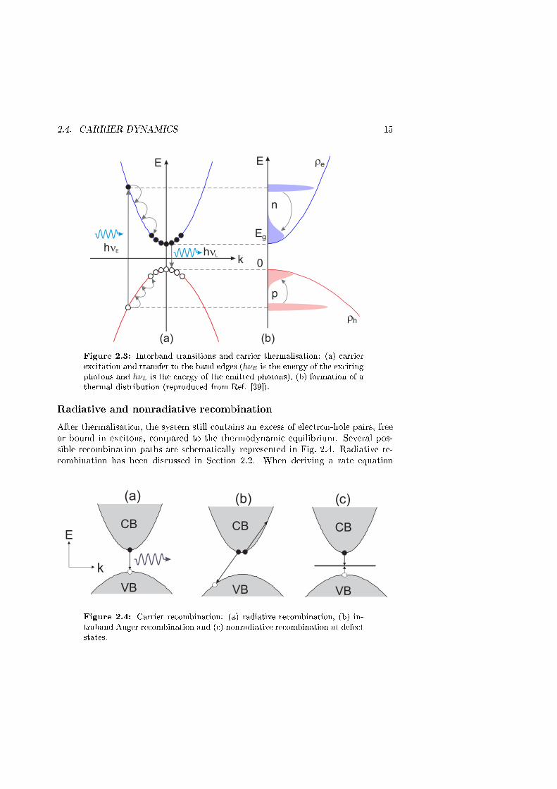
2.4. CARRIER DYNAMICS 15
hnE
k
E
hnL
n
E
p
re
rh
0
Eg
(a) (b)
Figure 2.3: Interband transitions and carrier thermalisation: (a) carrierexcitation and transfer to the band edges (hνE is the energy of the excitingphotons and hνL is the energy of the emitted photons), (b) formation of athermal distribution (reproduced from Ref. [39]).
Radiative and nonradiative recombination
After thermalisation, the system still contains an excess of electron-hole pairs, freeor bound in excitons, compared to the thermodynamic equilibrium. Several pos-sible recombination paths are schematically represented in Fig. 2.4. Radiative re-combination has been discussed in Section 2.2. When deriving a rate equation
(a) (b) c)
E
k
CB
VB
CB
VB
CB
VB
(
Figure 2.4: Carrier recombination: (a) radiative recombination, (b) in-traband Auger recombination and (c) nonradiative recombination at defectstates.

16 CHAPTER 2. OPTICAL TRANSITIONS AND CARRIER DYNAMICS
model for the carrier recombination in a LED, a simple expression for the spon-taneous recombination is derived from Eqs. (2.7) [40]. Far from degeneracy, theFermi-Dirac distributions for electrons and holes evaluated near the band edges areapproximately proportional to the total density of electrons and holes, n and p,respectively [41]: f1 ∝ n and f2 ∝ p. Exploiting this simpli�cation, the expressionsfor the spontaneous emission rate in Eqs. (2.7) can be integrated on the photonenergy to obtain ∫ ∞
Eg
RspdE ≈ Bnp, (2.16)
where B is the bimolecular recombination coe�cient.As for the nonradiative recombination, it can occur via Auger recombination
and recombination at defects or surface states. In the Auger recombination, therecombination energy is transferred to a third particle, electron or hole, that isexcited to a higher energy level. The higher energy level may be within the sameband as for an intraband Auger recombination or within a higher energy subband asin the case of an interband Auger recombination. The rate of Auger recombinationcan be expressed as
RAuger = ceehn2p+ cehhnp
2, (2.17)
where ceeh and cehh are usually considered as material constants. Auger processesrequire the interaction of three particles and become important only at high carrierdensities.
Defect states are associated with deviations from a perfectly periodic crystalstructure such as point defects, dislocations, stacking faults, inversion domains andthe external surface of the crystal. Crystal imperfections often introduce localizedelectronic states within the forbidden gap. Typically, localized states deep withinthe bandgap are more e�cient as nonradiative recombination centers than shallowdefects. This derives from the reduced probability of thermal escape of the trappedcarrier in a deep level and the increased probability of trapping a carrier with theopposite sign [42]. The energy from a nonradiative recombination is transferredto the lattice as heat. Therefore, strong nonradiative recombination in LEDs, be-sides reducing the IQE, causes self-heating and a reduction of the device operationlifetime [17].
The evolution of the electron and hole carrier densities, n and p respectively,after short pulse excitation can be described by means of a rate equation model.The Auger recombination and di�usion e�ects can be neglected to a �rst approxi-mation in semiconductors with relatively short carrier lifetimes and under moderateexcitation regime. A simple version that also excludes drift currents can be writtenas follows:
dn
dt= −Bnp− cnNn (2.18a)
dp
dt= −Bnp− cp(Nt −N)p. (2.18b)

2.5. TUNNELING AND THERMIONIC EMISSION 17
In these equations, B is the bimolecular recombination coe�cient and a single de-fect level has been considered. Electron and hole trapping rates at defect statesare proportional to the total densities of electrons and holes and to the densityof empty, N , and occupied, Nt − N , trap states, respectively. The proportion-ality constants are the electron and hole capture rates, cn and cp. Typically, thenonradiative recombination is a temperature-activated process and temperature de-pendent capture rates must be considered. When the nonradiative recombinationis dominant and the saturation of the trap states is negligible, n and p evolve withsingle exponential decays with time constants τe and τh, respectively. τe and τhcan be associated with the parameters in Eqs. (2.18) as follows:
1
τe= cnN (2.19a)
1
τh= cp(Nt −N). (2.19b)
From the expression for the total spontaneous recombination in Eq. (2.16), thePL signal follows an exponential decay with time constant τPL=(1/τe+1/τh)−1.Sometimes multiple decay constants are observed. Additional e�ects that mayexplain multiple decay constants are: multiple defect levels, saturation of the trapstates and descreening of internal �elds in polar QW structures.
2.5 Tunneling and thermionic emission
Besides radiative and nonradiative recombination, the electron and hole lifetimesin a QW LED may be determined by escape processes. Carrier escape out ofshallow wells and/or in case of thin barriers may occur via thermionic emission [43]and carrier tunneling [44]. The tunneling and thermionic emission of carriers arerepresented in Fig. 2.5. The escape mechanisms are in�uenced by the presence ofan electric �eld in the QW region. In this case, the potential pro�les in the well andbarrier regions assume a triangular shape. As a consequence, the energy level forcarriers within the QW moves toward the top of the well and the e�ective barrierthickness decreases. Thus the probabilities of tunneling and thermionic emissionincrease. The probabilities of tunneling and thermionic emission are characterizedin terms of tunneling and thermionic emission lifetimes, τt and τth, respectively.The tunneling lifetime is calculated as [45]
τt = τpexp
2
∫barrier
(2mb
~2[Ec,v(z)− E0]
)1/2dz
, (2.20a)
τp =
∫well
(2mw
E0 − Ec,v(z)
)1/2
dz, (2.20b)
where Ec,v(z) is the CB (VB) edge, E0 is the carrier energy level and mb is thee�ective mass in the barrier layers.

18 CHAPTER 2. OPTICAL TRANSITIONS AND CARRIER DYNAMICS
E0
Ec
tunnelling
thermionic emission
E
Eb
z
Figure 2.5: Schematic of the electron escape mechanisms from a QW: E0
is the carrier energy level and Eb is the height of the con�ning barrier.
Thermionic emission occurs for the electrons and holes in the high energy tailsof the carrier energy distributions. The sum of potential and kinetic energy forthese electrons and holes is larger than the con�nement potential. Therefore, theyare free to di�use outside the well region. The thermionic emission lifetime can becalculated as [43]
τth = Lw
(2πmw
kBT
)1/2
exp
(Eb − E0
kBT
), (2.21)
where Eb is the barrier height for the carrier escape, Lw is the well width and mw
is the e�ective mass in the well layer.

Chapter 3
Experimental techniques
In the experimental part of the thesis work, far-�eld (FF) EL and PL spectra weremeasured to reveal the general emission properties of the samples such as radiativetransition energy, spectral width and e�ective carrier temperature. TRPL wasemployed to study the recombination dynamics and the screening dynamics of theinternal �eld in QWs. Degenerate di�erential transmission pump-probe (DTPP)measurements were used to reveal the presence of localization and measure thelocalization depth in MQW structures. Additionally, the spatial distribution ofthe EL in AlGaN-based QW LEDs and of the PL in epitaxial layers was analyzedby means of NF spectroscopy. In this chapter, the general principles of the usedexperimental techniques are outlined and the speci�c setups brie�y described.
3.1 Laser system
The DTPP setup and the TRPL setup at KTH use the third harmonic pulses ofa mode-locked titanium-doped sapphire (Ti:Sapphire) laser (model Mira 900 byCoherent Inc.) as the excitation source. The third harmonic pulses were obtainedusing a setup that is schematically shown Fig. 3.1. The central wavelength of theTi:Sapphire laser pulses is tunable in the near-IR between 700 nm and 980 nm.The pulse duration is around 150 fs and the repetition rate is 76 MHz. The thirdharmonic of the Ti:Sapphire pulses is needed to excite band-to-band transitionsin AlGaN alloys. The third harmonic is obtained in two stages [46]. Firstly, thesecond harmonic generation is obtained focusing the near-IR pulses onto a lithiumtriborate (LBO) crystal. The near-IR and blue pulses are separated by a dichroicmirror that is highly re�ective in the blue region. The polarization of the bluepulses is rotated to be parallel with the one of the near-IR pulses. Moreover, thetemporal delay between near-IR and blue pulses is adjusted so that they perfectlyoverlap onto a barium borate (BBO) crystal. The third harmonic of the near-IR
19

20 CHAPTER 3. EXPERIMENTAL TECHNIQUES
Ti:Sapphire
LBO
l/2 plate
BBO
B-DM
B-DM
delay stage
UV-DM
w(h)
2w(v)
2w(h)
3w(v)
Figure 3.1: Third harmonic generation: second harmonic pulses are gen-erated inside the LBO crystal, dichroic mirrors (B-DM) are used to separatethe blue from IR pulses after the LBO crystal and to mix them again afterpolarization rotation and delay adjustment. Blue and IR pulses overlapinside the BBO crystal where UV pulses are generated by sum-frequency.Lastly, the UV pulses are separated by another dichroic mirror (UV-DM).
pulses is obtained by sum-frequency generation in the BBO crystal. The UV pulsesare separated by a dichroic mirror that is highly re�ective for the UV pulses. Thincrystals have to be used to minimize dispersion and pulse stretching inside thecrystals. To maximize conversion e�ciency, the beams have to be tightly focusedonto the crystals whose orientation must be adjusted to ful�ll the phase matchingcondition. Typical achieved average power of the third harmonic pulses with centralwavelength around 266 nm is about 30 mW, which corresponds to 5.3×10⁸ photonsper pulse.

3.2. FAR-FIELD TECHNIQUES 21
3.2 Far-�eld techniques
Time-resoved photoluminescence
TRPL is a contactless and non-destructive technique that is used to characterizethe carrier dynamics in semiconductors. Electron and hole pairs are generated inthe sample by means of short laser pulses that are tuned above the semiconductorbandgap. The excited carriers can be separated if a su�ciently strong electric �eldis present in the excited region as in the active region of a photodiode. Otherwise,they recombine via radiative or nonradiative recombination. Radiative recombina-tion gives rise to luminescence from the sample. Under the same conditions as inthe derivation of Eq. (2.16), the wavelength-integrated instantaneous luminescenceintensity is proportional to the instantaneous total electron and hole densities n(t)and p(t), respectively:
I(t) ∝ n(t)p(t). (3.1)
Therefore, the luminescence transient provides information on the recombinationdynamics such as the carrier lifetimes.
lenses
(electrons to light)
Figure 3.2: Operating principle of the streak camera (reproducedfrom Ref. [47]).

22 CHAPTER 3. EXPERIMENTAL TECHNIQUES
The streak camera is often used to obtain the temporal resolution in TRPLexperiments. Fig. 3.2 shows a schematic representation of the streak camera maincomponents and operation principle [47]. Often the luminescence is spectrally re-solved by coupling a spectrograph to the the streak camera input. The wavelengthcomponents of the light entering the instrument are separated along the directionof the streak camera entrance slit, which de�nes the direction of wavelength axis inthe �nal image. The amount of light entering the instrument can be modi�ed byadjusting the entrance slit width. A lens assembly inside the camera forms an imageof the slit onto the surface of a photocathode inside a vacuum tube. A number ofelectrons proportional to the photon �ux is emitted at every point of the photocath-ode surface. Inside the vacuum tube, the electrons are accelerated toward a pair ofde�ection plates with parallel orientation to the entrance slit of the instrument. Ahigh-speed sweep voltage is applied to the plates as the electrons stream betweenthem. The experienced de�ection by the electrons passing through the electrodesdepends on their arrival time. The direction of de�ection, that is normal to thedirection of the wavelength axis, de�nes the direction of the temporal axis in the�nal image. The de�ected electrons pass through a microchannel plate where theirnumber is multiplied. Finally, they hit a phosphor screen exciting �uorescence.The �uorescence image on the screen is read by a charge-coupled device camera.The �uorescence intensity at every point of the image is proportional to the pho-ton �ux at the corresponding wavelength and arrival time. The synchroscan modeallows accumulating multiple luminescence transients. Their correct synchroniza-tion is accomplished by detecting a replica of the excitation pulses that triggersthe voltage sweep. Fig. 3.3 shows a typical streak camera image. Wavelength andtemporal axes are also indicated for clarity. Two di�erent streak camera setupshave been used in the thesis experimental work. The streak camera at KTH is a
t
l
Figure 3.3: Example of streak camera image. Wavelength andtemporal axes are also indicated.

3.2. FAR-FIELD TECHNIQUES 23
Hamamatsu Universal Streak camera C5680 Series with time resolution of 2 ps.The duration of the measured dynamics is limited in this setup by the laser repe-tition rate to below 13 ns. The setup at Rensselaer Polytechnic Institute employsa Q-switched neodymium-doped yttrium aluminum garnet (Nd:YAG) laser. Thepulse central wavelength, duration and repetition rate are 1064 nm, 20 ps and 10Hz, respectively. The harmonics up to the �fth at 213 nm are obtained with theuse of multiple non-linear crystals. Moreover, the achievable pulse energy is of theorder of µ J for pulses with central wavelength at around 266 nm and correspondsto a four orders of magnitude larger photon �ux per pulse than for the setup atKTH. The streak camera is in this case a Hamamatsu single shot streak camerawith enhanced sensitivity in the UV. In this setup, the time resolution is limited bythe excitation pulse length. The slow laser repetition rate allows measuring longerluminescent transients.
Pump-probe setup
The DTPP setup allows measuring carrier dynamics with higher temporal resolu-tion than with a streak-camera-based setup. In the DTPP experiment, the timeresolution is limited by the pulse duration. Fig. 3.4 (a) shows a schematic represen-tation of the used setup for measuring the results in Paper VI. In the experiment,the third harmonic pulse train from the Ti:Sapphire laser is split into two beams -pump and probe - and separately focused on the same spot on the sample surface.The pump pulses are more intense and excite the electron and hole densities n0and p0, respectively, at the reference time t0. The presence of free carriers nearthe band edge modi�es the absorption coe�cient and the refractive index of thematerial from the unexcited values. If the temporal evolution of the many-bodye�ects can be neglected, the change of absorption coe�cient at photon energy hνcan be expressed as [48]
∆α(hν) = −α0(hν) (∆fe(Ee) + ∆fh(Eh)) , (3.2)
where α0(hν) is the absorption coe�cient of the unexcited semiconductor and Eeand Eh are the electron and hole levels, respectively, that are directly excited byphotons with energy hν. As mentioned in Section 2.4, the Fermi-Dirac distributionsfe(Ee) and fh(Eh) are proportional to the total electron and hole densities n andp, respectively. Therefore, Eq. (3.2) can be expressed in terms of n and p as
∆α(hν, t) = −α0(hν)(c1n(t) + c2p(t)), (3.3)
where c1 and c2 are two constants.The probe pulses are weaker and reach the sample with an adjustable temporal
delay t after t0. If the sample has a low optical density, the transmitted part of theprobe pulse train can be reliably measured. Because of the carrier recombination,the carrier densities n(t) and p(t) at the time t are reduced from the initial valuesn0 and p0 at time t0. As a consequence, the transmittivity usually decreases for

24 CHAPTER 3. EXPERIMENTAL TECHNIQUES
Probe
Pump Lock-inamplifier
detector
sample
delay stage
chopper
Dt
DT
Dt=0
(a)
(b)
Figure 3.4: Di�erential transmission pump-probe setup: (a) pump-probesetup, (b) typical pump-probe trace.
increasing delay time t between the pump and the probe. Referring to Eq. (3.3),the change of transmittivity is proportional to a weighted sum of electron and holedensities. In Fig. 3.4 (b), a typical pump-probe trace is shown. The maximumrelative change of transmittivity for the probe pulse is often fairly weak and lock-indetection is used to increase the sensitivity of the experiment. The pump signalis mechanically chopped at a lower frequency than the repetition rate of the laserpulses. The changes in the probe signal that have the same periodicity as thechopping frequency are �ltered from the total signal by means of lock-in detection.
3.3 Near-�eld microscopy
The optical transitions and carrier dynamics in III-nitride layers are strongly in�u-enced by crystal inhomogeneities. As a result of their presence, variations of thepeak wavelength, spectral width and luminescence intensity occur over the layersurface. Spatially resolved spectral measurements are of fundamental interest to
3.3. NEAR-FIELD MICROSCOPY 25
characterize the transport and luminescence properties of III-nitride-based lightemitters. On the other hand, the length scale at which the relevant phenomenaoccur is small and often beyond the resolution limit of conventional FF techniques.For this reason, NF spectroscopy has emerged as an important tool for semicon-ductor characterization. This chapter provides a short introduction to the conceptof optical NF and the related experimental techniques.
The di�raction limit
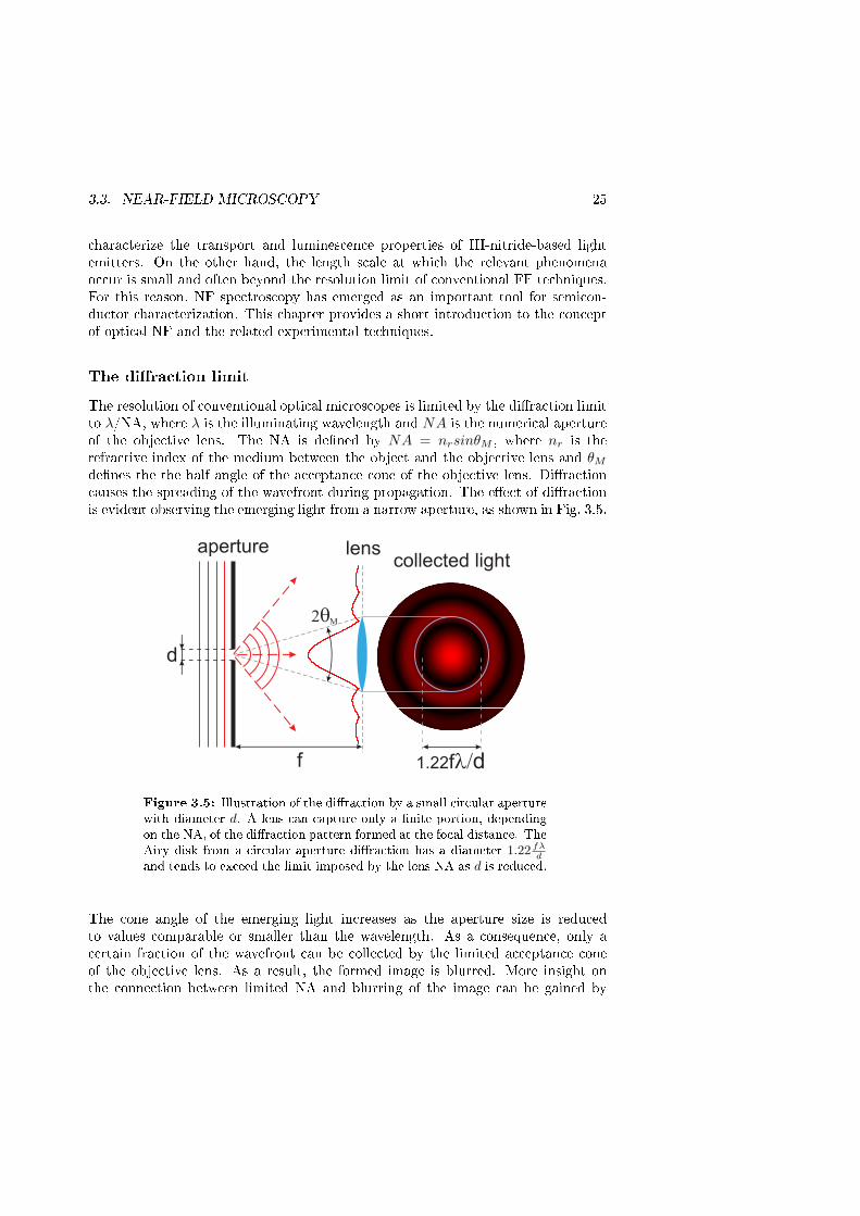
The resolution of conventional optical microscopes is limited by the di�raction limitto λ/NA, where λ is the illuminating wavelength and NA is the numerical apertureof the objective lens. The NA is de�ned by NA = nrsinθM , where nr is therefractive index of the medium between the object and the objective lens and θMde�nes the the half angle of the acceptance cone of the objective lens. Di�ractioncauses the spreading of the wavefront during propagation. The e�ect of di�ractionis evident observing the emerging light from a narrow aperture, as shown in Fig. 3.5.
f 1.22fl/d
d
aperture lenscollected light
2qM
Figure 3.5: Illustration of the di�raction by a small circular aperturewith diameter d. A lens can capture only a �nite portion, dependingon the NA, of the di�raction pattern formed at the focal distance. TheAiry disk from a circular aperture di�raction has a diameter 1.22 fλ
d
and tends to exceed the limit imposed by the lens NA as d is reduced.
The cone angle of the emerging light increases as the aperture size is reducedto values comparable or smaller than the wavelength. As a consequence, only acertain fraction of the wavefront can be collected by the limited acceptance coneof the objective lens. As a result, the formed image is blurred. More insight onthe connection between limited NA and blurring of the image can be gained by

26 CHAPTER 3. EXPERIMENTAL TECHNIQUES
means of the angular momentum representation which is introduced in the nextsubsection.
As in the case of the emerging light from a small aperture, all the �ne featuresof the object under observation generate widely diverging wave components whosepartial collection is responsible for the blurring of the obtained image. There arepractical limitations to the maximum achievable NA that limit the resolution ofstandard microscopes to values larger than λ/2 [49]. It can be shown that di�rac-tion is intrinsically associated with the propagation of electromagnetic waves. Onthe other hand, the �eld in the proximity of the source contains localized, non-propagating components. The non-propagating �eld components are evanescent,that is, they decay exponentially with the distance from the source. The region ofspace where the evanescent components are stronger than the propagating ones iscalled the NF [50]. The extent of the NF region does not depend on the wavelengthbut only on the source dimension [49]. This is an important di�erence between NFand the evanescent �eld produced by total internal re�ection. The NF microscopecircumvents the limitation of a �nite NA by moving an electric �eld probe in closeproximity of the source, where the evanescent components can be detected, therebyrealizing a high e�ective NA.
The angular momentum representation
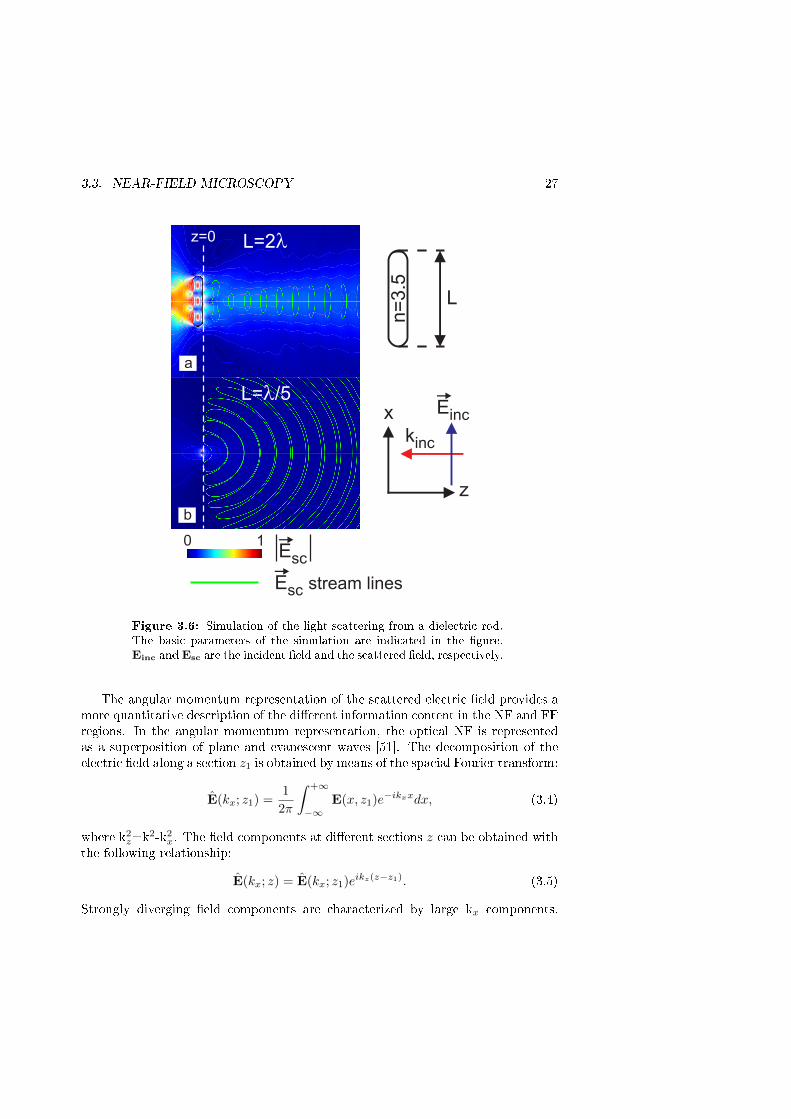
In this section, a more quantitative description of the NF is given in terms of theangular momentum representation. The connection between di�raction and mo-mentum representation is clari�ed by means of a two-dimensional electromagneticsimulation. The simulations were performed with the commercial software COM-SOL Multiphysics 3.5. Let us consider a dielectric �at rod aligned along the x axiswith the longer side equal to L and subwavelength thickness. A plane wave that ispolarized in the plane of the image impinges on the long side along the negative zdirection. In Fig. 3.6, the scattered �eld patterns for two values of the rod lengthare shown. The color scale represents the module of the scattered �eld, the redlines are the stream lines of the scattered electric �eld that are parallel in everypoint to the �eld vector. In Fig. 3.6 (a), the side of the rod is much longer than theincident wavelength and the scattered �eld along z propagates with approximatelyplane waves. The length L of the rod can be determined to a good accuracy fromthe size of the wavefront in the FF. As the rod dimension L is reduced, the scat-tered �eld tends to diverge laterally while propagating away from the rod. As thelateral dimension of the rod is reduced below the wavelength of the incident lightas in Fig. 3.6 (b), the scattered �eld pattern resembles the one from an electricdipole. At this point, the information on the lateral dimension of the rod cannotbe retrieved from a FF measurement. The module of the scattered �eld acrosstwo sections at distance z1=λ /100 and z2=4λ are shown in Fig. 3.7 (a) and (b),respectively. The �eld pattern in close proximity of the rod retains the informationon the rod dimension. This simple observation justi�es the use of NF detection tobreak though the di�raction limit.
3.3. NEAR-FIELD MICROSCOPY 27
L=2l
L=l/5
L
x
z
kinc
n=
3.5
00.10.20.30.40.50.60.70.80.910 0.1 0.2 0.3 0.4 0.5 0.6 0.7 0.8 0.9 1 Esc
0 1
E stream linessc
z=0
Einc
a
b
Figure 3.6: Simulation of the light scattering from a dielectric rod.The basic parameters of the simulation are indicated in the �gure.Einc and Esc are the incident �eld and the scattered �eld, respectively.
The angular momentum representation of the scattered electric �eld provides amore quantitative description of the di�erent information content in the NF and FFregions. In the angular momentum representation, the optical NF is representedas a superposition of plane and evanescent waves [51]. The decomposition of theelectric �eld along a section z1 is obtained by means of the spacial Fourier transform:
E(kx; z1) =1
2π
∫ +∞
−∞E(x, z1)e−ikxxdx, (3.4)
where k2z=k2-k2x. The �eld components at di�erent sections z can be obtained with
the following relationship:
E(kx; z) = E(kx; z1)eikz(z−z1). (3.5)
Strongly diverging �eld components are characterized by large kx components.

28 CHAPTER 3. EXPERIMENTAL TECHNIQUES
x, l-12 -8 -4 0 4 8 12
IE
scI,
arb
. u
nits
z=l/100
(a) (b)
-12 -8 -4 0 4 8 12
x, l
0 1 2 3 4
kx, k
0
evanescent
0 1 2 3 4
kx, k
0
evanescent
IE
y-s
c I, a
rb. units
z=4l
L=8l L=2l L= l L= /5l L= /20 l dipole
(d)c)(
Figure 3.7: Scattered �eld magnitude at a distance z1=λ /100 (a) andz2=4λ (b) from a rod of length L. Several rod lengths L are considered.(c) and (d) show the angular momentum representation of the y-polarizedcomponent of the scattered �eld at the same positions.
There is no limitation to kx<k, thus kz is free to become imaginary. The com-ponents for which this happens become evanescent and constitute the NF.
In Fig. 3.7 (c) and (d), the Fourier transform of the y-component of the electric�eld along the sections z1 and z2 is shown. There is an evident loss of spectralcomponents as the �eld propagates away from the scattering source. The sourcegeometry determines the kx bandwidth of the optical signal in the NF. In fact,
3.3. NEAR-FIELD MICROSCOPY 29
the �eld in close proximity of the source reproduces the surface geometry. Hence,the high kx components are associated with the small features of the surface. Theloss of high spatial frequency components corresponds to a low pass �ltering of theobject geometry and generates the blurring e�ect in the reconstructed image. Inparticular, sub-wavelength features generate evanescent �eld components that, byde�nition, do not reach the FF. This establishes an intrinsic limit to the resolutionof FF microscopes.
The angular momentum representation elucidates how the dimension of the NFdepends on the dimension of the source. The decay length of the NF is determinedby the relationship between kx and kz, thus, by the source geometry. Anotherconclusion that can be drawn from the angular momentum representation is thatthe NF does not contribute to the propagation of energy. The base functions inthe angular momentum representation in Eq. (3.4) are orthonormal. Hence, thetotal power emitted from the source can be computed as the sum of the power ineach �eld component or �mode�. The evanescent components decay within the NFregion. Therefore, they do not contribute to the power transmission to the FF.
Near-�eld probes
The detection of the evanescent components of the source �eld requires their trans-formation from evanescent to propagating [49]. This is obtained by perturbing theoptical NF with a probe. Sensitive detection requires the separation of the gener-ated waves by the probe - the secondary waves - from the rest of the signal comingfrom the source. The resolution of the measurement is limited by the dimension ofthe probe. However, it should be reminded that the presence of the probe perturbsthe original NF at the source. Therefore, it is not possible to separate the originalNF from the probe-sample interaction in the results of real measurements. As aconsequence, measurement artifacts may occur [52].
In a common implementation of the NF microscope, a tapered optical �beris used as a probe. Several measurement con�gurations are possible [51]. In thecollection mode setup, a �ber probe is used to guide the scattered �eld from theNF region around the tip to the detector, while the illumination source is in theFF. No external light sources are required in case of EL NF measurements. Inthe illumination mode, the probe is used to illuminate the sample in NF and thedetection occurs in the FF. Lastly, illumination and collection can be both guidedthrough the �ber in the illumination/collection (IC) setup. The latter operationmode simpli�es the NF measurements on opaque samples.
The �ber tips employed in this work were obtained with the tube etching method[53]. The etching solution that is contained inside a Te�on vessel is composed by 50% water solution of hydro�uoric acid covered by a few millimeters thick isooctanelayer. The isoocatne layer prevents the evaporation of the acid from the vessel.The tip is vertically dipped in the solution at room temperature. The etchingprocess takes a variable amount of time depending on the �ber composition anddiameter; the obtained tip quality can also vary greatly [54]. The etching process

30 CHAPTER 3. EXPERIMENTAL TECHNIQUES
fresh HF products
(b) c)
(d)
(a) (
Figure 3.8: Tube etching: (a) the �ber probe is immersed in the HF so-lution with the jacket, (b) symmetrical thinning, (c) formation of a conicaltip, (d) convection of fresh HF, indicated with dashed lines, and reactionproducts, indicated with dotted lines (adapted from Ref. [53]).
is schematically represented in Fig. 3.8. Initially, the �ber is symmetrically thinnedproducing a long sharp appendix that was often observed in underetched tips. Asthe thin appendix is etched away, only the conical part at the meniscus of the tipremains. As soon as a preliminary taper is formed, convection starts to deliver HFto the upper region of the cone as shown in Fig. 3.8 (d). Convection is driven byconcentration gradients caused by the etching process itself and the gravitationalremoval of the reaction products [53]. Tube etching produces a more homogeneoustip surface and more reproducible tip geometry than tubeless etching. After theetching process is completed, the �ber is repeatedly rinsed with ethanol and water.Lastly, the jacket is mechanically removed from the tip and the naked tip rinsedagain.
Basic guidelines to establish the desired properties for an optical �ber probe areprovided by a simpli�ed model of the dipole-dipole interaction as described in Ref.[49]. The model reveals that the highest contrast is achieved for �eld distributionof comparable dimension with the probe apex diameter. Furthermore, there is atrade-o� between throughput and contrast depending on the value of the taper coneangle. Decreasing the cone angle, the contrast improves by collecting less �eld fromthe taper region but the propagation losses in the longer taper are larger, vice versafor larger cone angles.
Usually, optical �ber probes are coated with a thin metal layer to prevent FF
3.3. NEAR-FIELD MICROSCOPY 31
collection from the taper of the tip. Reproducible apertures can be obtained on thecoated tip using a focused ion beam. However, sub-wavelength resolution with un-coated �ber probes has also been theoretically predicted [55, 56] and experimentallyveri�ed [57, 58] in the IC setup. Metal-coated probes are believed to be superiorto uncoated probes with respect to spatial resolution and contrast because theirsmall apertures represent well-de�ned subwavelength radiation sources or detectors[59]. However, there are some important advantages of using uncoated probes. Thefabrication of uncoated probes is simpler and less time consuming. Moreover, thedetected optical signal is usually stronger for uncoated probes, though sometimes atthe expense of the lateral resolution. Uncoated tips can also sustain larger opticalpowers without the risk of melting or detaching the metal coating. Furthermore, thetip is more resistant to wearing out and to topographically induced image artifactsdue to formation of metallic protrusions. Lastly, the larger throughput enables asimpler implementation of the IC setup.
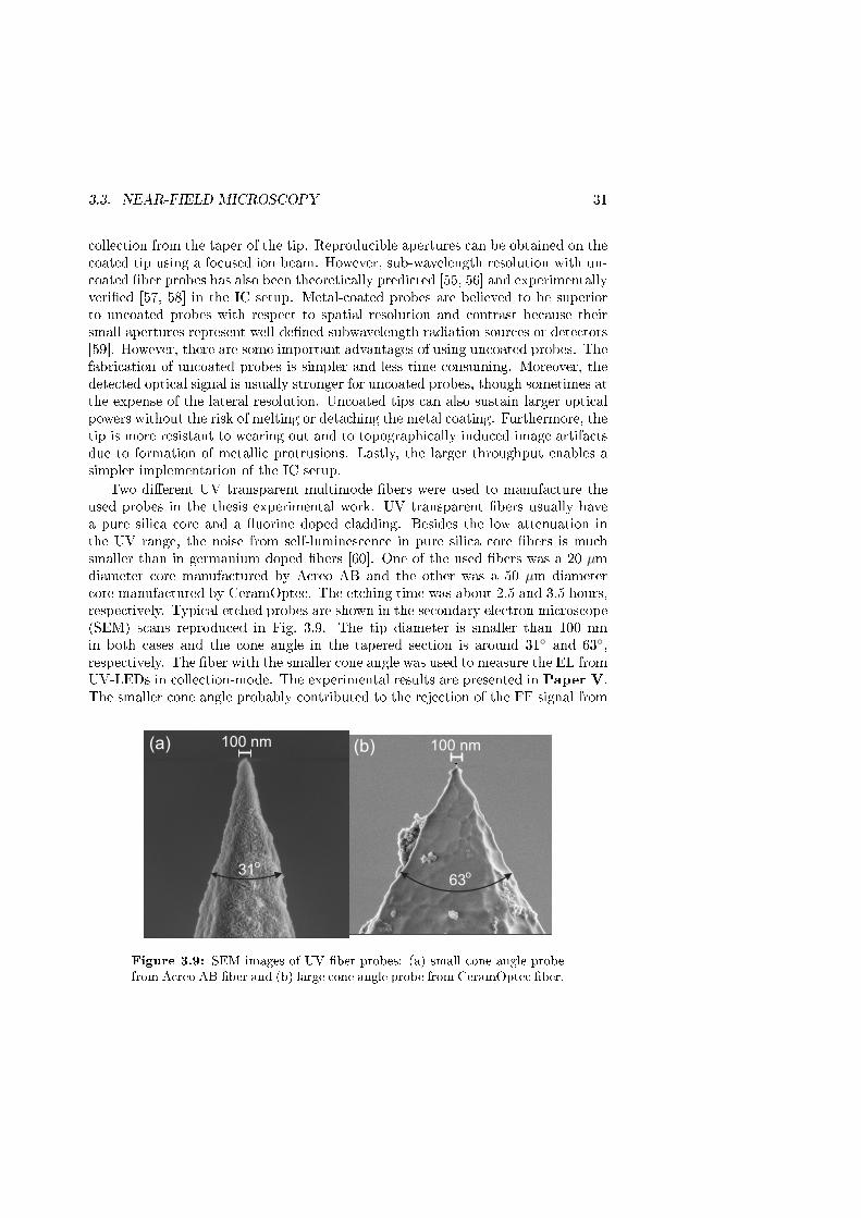
Two di�erent UV transparent multimode �bers were used to manufacture theused probes in the thesis experimental work. UV transparent �bers usually havea pure silica core and a �uorine doped cladding. Besides the low attenuation inthe UV range, the noise from self-luminescence in pure silica core �bers is muchsmaller than in germanium doped �bers [60]. One of the used �bers was a 20 µmdiameter core manufactured by Acreo AB and the other was a 50 µm diametercore manufactured by CeramOptec. The etching time was about 2.5 and 3.5 hours,respectively. Typical etched probes are shown in the secondary electron microscope(SEM) scans reproduced in Fig. 3.9. The tip diameter is smaller than 100 nmin both cases and the cone angle in the tapered section is around 31◦ and 63◦,respectively. The �ber with the smaller cone angle was used to measure the EL fromUV-LEDs in collection-mode. The experimental results are presented in Paper V.The smaller cone angle probably contributed to the rejection of the FF signal from
100 nm
o63o31
100 nm(a) (b)
Figure 3.9: SEM images of UV �ber probes: (a) small cone angle probefrom Acreo AB �ber and (b) large cone angle probe from CeramOptec �ber.

32 CHAPTER 3. EXPERIMENTAL TECHNIQUES
the tapered part of the probe. In this operation mode, it is hardly possible to makeclaims on subwavelength resolution from a theoretical standpoint. However, thea posteriori inspection of the measurements recorded with a photomultiplier tube(see Fig. 3.10) reveals the presence of well de�ned features which do not seem tobe induced by the sample morphology.
(a)
(d)(b)
4mm 4mm
(c)
Figure 3.10: Photomultiplier-tube scans of a UV LED surface. Panels(a) and (c) are show the topography and panels (b) and (d) spectrallyintegrated EL intensity from the corresponding regions.
Furthermore, the published spectral measurements are not a�ected by topographi-cal artifacts. The results show sub-micrometer-sized regions emitting at a di�erentwavelength from the FF background.
In the case of IC NF spectroscopy, the signal level is critical. The excitationintensity that is coupled into the �ber is limited by the damage threshold and thenoise generation in the �ber. Moreover, the excitation intensity is further decreasedby the re�ection and losses during propagation in the tapered part of the �ber. Onthe other hand, the IC setup was found to improve the spatial resolution of themeasurement with respect to the collection-mode setup with uncoated probes. Thelarger cone angle and lower noise generation of the probes that were manufacturedfrom the CeramOptec �ber was well-suited for the IC measurements presented inPaper VIII.
3.3. NEAR-FIELD MICROSCOPY 33
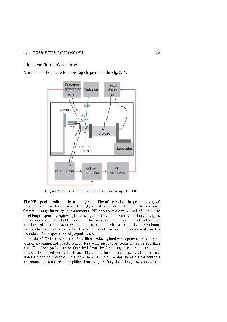
The near-�eld microscope
A scheme of the used NF microscope is presented in Fig. 3.11.
Function generator Detector
Piezodriver
preamplifierlock-in amplifier
PI controller
Nanocube
y-piezo
diether piezo
fiber
TF
sample
OUT
IN
OUT
Figure 3.11: Scheme of the NF microscope setup at KTH.
The NF signal is collected by a �ber probe. The other end of the probe is coupledto a detector. In the thesis work, a UV-sensitive photo multiplier tube was usedfor preliminary intensity measurements. NF spectra were measured with a 0.5 mfocal length spectrograph coupled to a liquid nitrogen-cooled silicon charge-coupleddevice detector. The light from the �ber was collimated with an objective lensand focused on the entrance slit of the instrument with a second lens. Maximumlight collection is obtained when the f-number of the coupling optics matches thef-number of the spectrograph, equal to 6.5.
In the SNOM setup, the tip of the �ber probe is glued with epoxy resin along onearm of a commercial quartz tuning fork with resonance frequency at 32.768 KHz[61]. The �ber probe can be detached from the fork using acetone and the samefork can be reused with a fresh tip. The tuning fork is magnetically attached to asmall segmented piezoelectric tube - the dither piezo - and the electrical contactsare connected to a current ampli�er. During operation, the dither piezo vibrates the
34 CHAPTER 3. EXPERIMENTAL TECHNIQUES
tuning fork-�ber probe assembly. The oscillation frequency of the dither is set by afunction generator at the resonance frequency. The mechanical vibration of the forkgenerates a current which is ampli�ed and fed to a lock-in ampli�er. Interestingly,a subnanometer vibration of the center of mass of the tuning fork at resonance issu�cient to generate a measurable current [62]. Therefore, the lateral vibration ofthe tip above the sample does not a�ect the resolution of the experiment.
The principle of the probe-to-sample distance control is based on the detectionof the shear force between the tip and the sample. In the setup, a proportional-integral controller uses the amplitude signal to adjust the probe-to-sample distanceby driving a second piezoelectric tube. While scanning the sample surface, thefriction forces between the sample and the tip tend to damp the amplitude of thetip oscillations. The probe-to-sample distance is adjusted as to keep the oscilla-tion amplitude constant. Thus, the use of the shear force as the feedback impliesa constant gapwidth between the tip and the sample. In general, the use of theoptical signal as feedback is possible as well. However, it produces a less accu-rate distance control [51] because the collected signal is neither short-ranged normonotonously dependent on the probe-sample distance. The nature of the frictionforces is most probably related to mechanical damping that is mediated throughadsorbate �lling in the tip sample gap [62], particularly in the case of atmosphericpressure experiments.

Chapter 4
Basic properties of III-nitrides
This chapter provides an introduction to the basic properties of the wurtzite III-nitrides with particular emphasis on the AlGaN alloys.
4.1 Nitrides for light emitters
The group III-nitrides include indium nitride (InN), GaN, AlN and their ternaryand quaternary alloys. Although other alloys belong to the same family, for examplethose containing boron nitride (BN), they have attracted signi�cantly less attentionso far and they will not be considered in the following. In the wurtzite polytype,III-nitride alloys exhibit direct bandgaps for all compositions. Their bandgap canbe tuned by alloying in the range from 0.7 eV for InN, through 3.42 eV for GaN, upto 6.25 eV for AlN, as shown in Fig. 4.1. The breadth of this interval, which spansfrom the IR through all the visible range up to deep-UV, makes the III-nitrideshighly attractive for the production of light emitters.
As light-emitting materials, GaN-based alloys are superior at present to theother available wide bandgap materials - SiC, zinc selenide (ZnSe) and zinc oxide(ZnO). The indirect bandgap of SiC limits the luminescence e�ciency of this ma-terial. The poor electronic properties, low thermal conductivity and weak bondstrength in ZnSe-based alloys determine a very short operation lifetime for ZnSe-based devices [64]. Although ZnO-based alloys may eventually become competitivewith III-nitride alloys, they still su�er from low luminescence e�ciency and unsta-ble and non-reproducible p-type doping [65]. The IQE of InGaN-based LEDs canbe as high as 70% [66, 67] and there are indications that comparable values maybe achieved in AlGaN-based devices as well [13]. In principle, III-nitride-based de-vices are able to operate in high-temperature environments due to their high bondstrength. Additionally, the III-nitrides exhibit good thermal conductivity, whichallows e�cient heat dissipation from devices operating in high-current conditions
35
36 CHAPTER 4. BASIC PROPERTIES OF III-NITRIDES
3.20 3.40 3.60
1
2
3
4
5
6
1240
620
413
310
248
207
InN
GaN
linear interp. with bowing
l,
nm
ba
nd
ga
p,
eV
in-plane lattice constant, Å
AlN
Figure 4.1: Bandgap energy and corresponding wavelength as a functionof the in-plane lattice constant a of III-nitrides at room temperature. Thered dashed line is the linear interpolation of the values for the binary com-pounds, the black line includes the bowing e�ect (calculated values usingthe constants in Ref. [63]).
such as high-brightness LEDs [68]. Unfortunately, these advantageous propertieshave been only partially harnessed by the deep-UV technology so far. The poorthermal conductivity of the normally employed sapphire substrates [16] and thehigh density of native extended defects are among the limiting factors. The ex-tended defects are thought to reduce the operation lifetime of AlGaN-base devicesat high current/temperature operating conditions [69, 70] (see Section 5.5). Someimportant properties of the AlN and GaN binary compounds are summarized inAppendix A.1.
Crystal structure
The thermodynamically most stable phase of the III-nitrides is the wurtzite struc-ture [71]. In Fig. 4.2, the GaN wurtzite crystal structure is shown and the latticeconstants c and a are de�ned. The projection on the c-plane (0001) in Fig. 4.2 (b)evidences the hexagonal symmetry. The wurtzite group-III nitrides lack an inver-sion symmetry plane perpendicular to the c-axis (the c-axis is indicated in Fig. 4.2

4.1. NITRIDES FOR LIGHT EMITTERS 37
(a) (b)
c
a
N Ga
[1120]
[1100]
[0001]
[1120] [1100][0001]
Figure 4.2: Ga-face wurtzite crystal structure of GaN: (a) projectionon the a-plane (1120), (b) projection on the c-plane (0001). The violetparallelepiped contains the primitive unit cell. The lattice constants c anda are indicated with black arrows. The green dashed arrow representsthe electrostatic interaction between non-bonded anion-cation pairs alignedalong the c-axis (the structure was drawn with the software VESTA).
with its Bravais-Miller index [0001]). As a consequence, two possible stacking or-ders can be distinguished. If the bonds along the c-axis in the direction of growthgo from a metal atom to a nitrogen (N) atom, the layer has a (Ga,In,Al)-polarity -otherwise a N-polarity. The polarity of nitride epitaxial layers determines the signof the polarization charge in heterostructures (see Section 4.2).
AlGaN band structure
In Fig. 4.3 (a), a portion of the bulk GaN VB structure near k = 0 is represented[72]. The considered direction of the k-vector are within the c-plane, kt, and alongthe c-axis, kz. In the represented region, the VB is split into three subbands,denominated heavy hole (HH), light hole (LH) and crystal-�eld split-o� hole (CH)bands. The energy di�erence between the top of the HH and LH bands is onlyaround 10 meV, thus, holes from both the bands contribute to the lumnescenceat room temperature. The dashed lines represent the e�ect of an in-plane biaxialcompressive strain. This case is of particular interest because the well layers ofdeep-UV AlGaN-based LEDs are often under compressive strain. In general, strain
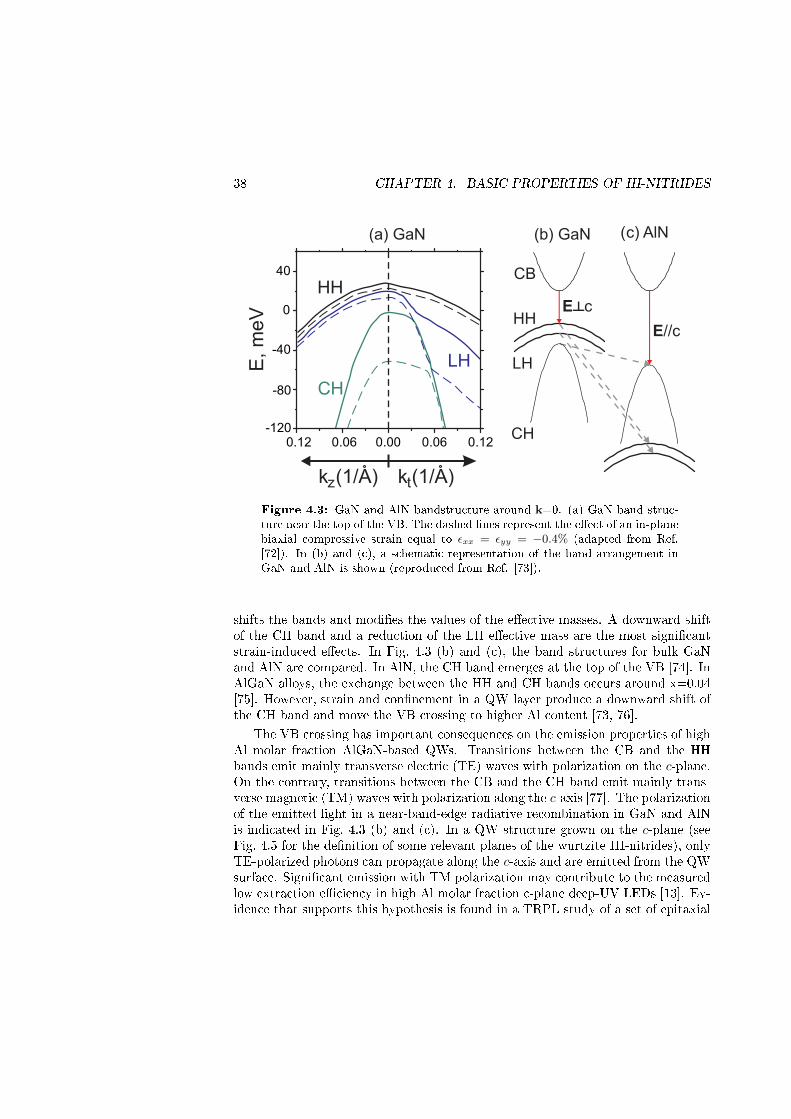
38 CHAPTER 4. BASIC PROPERTIES OF III-NITRIDES
0.12 0.06 0.00 0.06 0.12-120
-80
-40
0
40E
, m
eV
HH
LH
CH
kz(1/A) kt(1/A)
CB
HH
LH
CH
(a) GaN (b) GaN c) AlN
E//c
E c┴
(
Figure 4.3: GaN and AlN bandstructure around k=0. (a) GaN band struc-ture near the top of the VB. The dashed lines represent the e�ect of an in-planebiaxial compressive strain equal to εxx = εyy = −0.4% (adapted from Ref.[72]). In (b) and (c), a schematic representation of the band arrangement inGaN and AlN is shown (reproduced from Ref. [73]).
shifts the bands and modi�es the values of the e�ective masses. A downward shiftof the CH band and a reduction of the LH e�ective mass are the most signi�cantstrain-induced e�ects. In Fig. 4.3 (b) and (c), the band structures for bulk GaNand AlN are compared. In AlN, the CH band emerges at the top of the VB [74]. InAlGaN alloys, the exchange between the HH and CH bands occurs around x=0.04[75]. However, strain and con�nement in a QW layer produce a downward shift ofthe CH band and move the VB crossing to higher Al content [73, 76].
The VB crossing has important consequences on the emission properties of highAl molar fraction AlGaN-based QWs. Transitions between the CB and the HHbands emit mainly transverse electric (TE) waves with polarization on the c-plane.On the contrary, transitions between the CB and the CH band emit mainly trans-verse magnetic (TM) waves with polarization along the c-axis [77]. The polarizationof the emitted light in a near-band-edge radiative recombination in GaN and AlNis indicated in Fig. 4.3 (b) and (c). In a QW structure grown on the c-plane (seeFig. 4.5 for the de�nition of some relevant planes of the wurtzite III-nitrides), onlyTE-polarized photons can propagate along the c-axis and are emitted from the QWsurface. Signi�cant emission with TM polarization may contribute to the measuredlow extraction e�ciency in high Al molar fraction c-plane deep-UV LEDs [13]. Ev-idence that supports this hypothesis is found in a TRPL study of a set of epitaxial

4.1. NITRIDES FOR LIGHT EMITTERS 39
layers with di�erent Al molar fractions [78]. Comparable values of PL decay timewere measured among the samples. This indicates that there were not signi�cantdi�erences of nonradiative recombination rate. However, the samples with higherAl molar fractions exhibited reduced values of total PL intensity.
A precise calculation of the carrier distribution in the bands requires the knowl-edge of the band splitting and e�ective mass for each band. However, these valuesare a�ected by considerable uncertainty in the relaxed materials. Additionally, theuncertainty on the extent of the strain-induced modi�cations is even larger. Thesituation is greatly complicated in AlGaN heterostructures where extended defectsand alloy �uctuations may induce partial strain relaxation [13]. In the approachthat was followed in the calculations of Paper II and Paper III, only the holes inthe HH band were considered and the linear interpolations of the e�ective massesin relaxed GaN and AlN was used (see Appendix A.1). Similar calculations forAlGaN/GaN QWs have con�rmed that holes occupy mainly the �rst HH subbandfor a wide range of excitation levels [79].
Excitons in nitrides
The binding energy of excitons is large in III-nitrides [80, 81]. Table 4.1 reports thebinding energy and Bohr radius for bulk Wannier type excitons in GaN and AlN.The exciton binding energy is further enhanced in con�ned structures [82].
GaN AlN
Binding energy (meV) 28 44
Bohr radius (Å) 30 19
Table 4.1: Exciton properties of GaN and AlN [80, 81]
In GaN, excitons may form with holes in the HH, LH and CH bands and areknown as excitons A, B and C, respectively. All three exciton types were observedup to room temperature [83]. The spectral broadening of the exciton absorptionand emission lines in AlGaN alloys makes their direct observation more di�cult.However, the presence of fairly deep localization minima in AlGaN epitaxial lay-ers [84] and QWs (see Paper VI) increases the stability of the excitons againstthermal and electric �eld ionization. The radiative lifetime of localized excitonsin potential minima increases with the localization depth [24]. Additionally, local-ization prevents nonradiative recombination at dislocations [85], thereby increasingthe exciton lifetime.
In order to establish the role of exciton recombination in light-emitting devices,it is necessary to evaluate the stability of excitons at the carrier densities typicalfor device operation. In a 4 nm GaN/AlGaN QW, the Mott density was calculatedas 1.9×1012 cm−2 [86, 87] and around 1×1019 cm−3 in bulk GaN [88]. Thesedensities may be reached in high-brightness InGaN-based LEDs [89]. Much lower

40 CHAPTER 4. BASIC PROPERTIES OF III-NITRIDES
carrier densities are typically reached in AlGaN/AlGaN LEDs that are usuallydriven at lower currents [90]. Actually, considering the transparency carrier densityof 4.5×1012cm−2 in InGaN-based QWs [91], excitonic e�ects may be relevant evenin laser diodes [92].
4.2 Polarization �elds
Strong polarization �elds in III-nitride heterostructures have important consequenceson the luminescence and carrier transport in nitride-based LEDs. The existence ofa macroscopic polarization in III-nitride layers was �rst predicted from ab initio cal-culations by Bernardini and Fiorentini [93]. The experimental con�rmation followedshortly after [94]. Typically, the polarization of QW structures is experimentallydetermined from PL measurements. In this section, the polarization properties ofAlGaN heterostructures are reviewed and PL-based measurements of the polariza-tion constants are described.
The origin of the polarization charge
Fig. 4.4 shows the disposition of the bonds around a Ga atom in the wurtzite,Ga-face GaN crystal.
p0
N
N
N N
Ga
-
+
[0001]
p0p0
p0
pTOT
Figure 4.4: Bond distribution around a Ga atom in the wurtzite,Ga-face GaN (reproduced from Ref. [71]).
A similar arrangement, where four N atoms surround every group-III metal atom,occurs in all III-nitride crystals. N is more electronegative than group III atoms.As a result, a fractional negative charge accumulates close to the N atom in everycovalent bond of the crystal. Hence, every bond in the crystal is associated witha permanent dipole moment, p0, in units of Cm. p0 is represented in Fig. 4.4with a green arrow pointing from the negative charge around the N atom to the

4.2. POLARIZATION FIELDS 41
positive charge around the Ga atom. The sum of the four dipole moments aroundevery group-III atom would add to zero in the ideal wurtzite structure, where thebonds are arranged as a perfect tetrahedron. However, the electrostatic interactionbetween non-bonded anion-cation pairs, represented with a green dashed arrow inFig. 4.2, compresses the ideal tetrahedral structure along the c-axis [95]. As aresult, the dipole moment along the c-axis is not compensated by those o� the axis.The red arrow in Fig. 4.4 represents the net dipole moment, pTOT, around everyGa atom. The density of pTOT constitutes the spontaneous polarization, Psp, inunits of Cm−2. The alignement of pTOT along the c-axis explains why the planesthat are parallel to the c-axis are not polar, as shown in Fig. 4.5.
m
-pla
ne
c-plane
a-plane
[0001]
Psp
(b)(a)
a-planes
m-planes
Figure 4.5: Some wurtzite crystallographic planes: (a) conventionalunit cell displaying a c-plane (polar), a-plane (non-polar) and m-plane(non-polar); (b) projection on the c-plane (0001). The direction of thec-axis and Psp for a Ga-face crystal are also indicated (adapted fromRef. [13]).
Strain contributes to the total deformation of the crystal from the ideal wurtzitestructure as well and it alters the value of pTOT. The strain-induced contributionto the total polarization is known as piezoelectric polarization, Ppz. The totalpolarization P = Psp +Ppz within each lattice c-plane corresponds to �xed polar-ization charge densities +σb and -σb at the two interfaces of the plane. P is relatedto the surface bound charge density as
P · n = σb, (4.1)
where n is the unit vector normal to the surface. Within the material, the con-tributions from adjacent planes cancel each other. However, in correspondence ofthe external boundaries or at the interface between layers with di�erent composi-tions, a net surface charge remains uncompensated. The presence of a �xed chargesheet at the interface between nitride layers gives rise to intense polarization �eldsinside QW structures. The actual sign of the net surface charge densities and thedirection of the electric �elds in a heterostructure depend on the di�erence of totalpolarization P between adjacent layers.
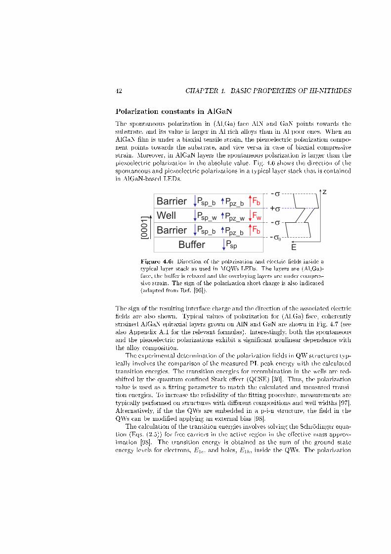
42 CHAPTER 4. BASIC PROPERTIES OF III-NITRIDES
Polarization constants in AlGaN
The spontaneous polarization in (Al,Ga)-face AlN and GaN points towards thesubstrate, and its value is larger in Al-rich alloys than in Al-poor ones. When anAlGaN �lm is under a biaxial tensile strain, the piezoelectric polarization compo-nent points towards the substrate, and vice versa in case of biaxial compressivestrain. Moreover, in AlGaN layers the spontaneous polarization is larger than thepiezoelectric polarization in the absolute value. Fig. 4.6 shows the direction of thespontaneous and piezoelectric polarizations in a typical layer stack that is containedin AlGaN-based LEDs.
Fb
Fw
Buffer
Barrier
Well
Barrier Psp_b
Psp_w
Psp_b
Psp
Ppz_b
Ppz_w
Ppz_b
Fb
-s0
-s
+s
-s
E
z
[0001]
Figure 4.6: Direction of the polarization and electric �elds inside atypical layer stack as used in MQWs LEDs. The layers are (Al,Ga)-face, the bu�er is relaxed and the overlaying layers are under compres-sive strain. The sign of the polarization sheet charge is also indicated(adapted from Ref. [96]).
The sign of the resulting interface charge and the direction of the associated electric�elds are also shown. Typical values of polarization for (Al,Ga)-face, coherentlystrained AlGaN epitaxial layers grown on AlN and GaN are shown in Fig. 4.7 (seealso Appendix A.1 for the relevant formulas). Interestingly, both the spontaneousand the piezoelectric polarizations exhibit a signi�cant nonlinear dependence withthe alloy composition.
The experimental determination of the polarization �elds in QW structures typ-ically involves the comparison of the measured PL peak energy with the calculatedtransition energies. The transition energies for recombination in the wells are red-shifted by the quantum con�ned Stark e�ect (QCSE) [30]. Thus, the polarizationvalue is used as a �tting parameter to match the calculated and measured transi-tion energies. To increase the reliability of the �tting procedure, measurements aretypically performed on structures with di�erent compositions and well widths [97].Alternatively, if the the QWs are embedded in a p-i-n structure, the �eld in theQWs can be modi�ed applying an external bias [98].
The calculation of the transition energies involves solving the Schrödinger equa-tion (Eqs. (2.5)) for free carriers in the active region in the e�ective mass approx-imation [98]. The transition energy is obtained as the sum of the ground stateenergy levels for electrons, E1e, and holes, E1h, inside the QWs. The polarization

4.2. POLARIZATION FIELDS 43
0.0 0.3 0.6 0.9
-0.12
-0.08
-0.04
0.00
PSP
GaN PPZ
p
ola
riza
tion
, C
/m2
xAl
AlNPPZ
GaNPTot
AlNPTot
Figure 4.7: Polarization of AlGaN layers (calculated values using theconstants in Ref. [63]). The Ppz is calculated for coherently strainedlayers on GaN (in red) and on AlN (in blue).
charges enter in the Schrödinger equation via the polarization-induced modi�cationof the potential pro�le in CB and VB. A term equal to ∆U(z) = qV (z) must beadded to the potential energy in Eq. (2.5b), where V (z) is calculated according tothe Poisson equation [32]:
d
dz
(ε(z)
dV (z)
dz+ P (z)
)= −ρ(z). (4.2)
In the Poisson equation, P (z) is the total internal polarization as given by thesum of the spontaneous and piezoelectric polarizations (in C/m−2) and ρ(z) is thecharge density (in C/m−3) that is associated with free carriers. ρ(z) is usually setto zero in the calculation of the PL peak energy under low excitation. Sometimes,the Schrödinger equation is modi�ed to account for the presence of excitons [97].
A di�erent approach makes use of the screening of the electric �eld by free-carrierinjection [79]. Screening occurs when a high density of free carriers in the activeregion counterbalances the polarization �eld. In this case, the PL peak energy shiftrather than its absolute value is compared with calculated values. In case of shortpulse excitation, dynamic descreening of the internal �eld can also be observed [79].
In Paper I, the value of polarization charge in QWs within a p-i-n structure wasdetermined making use of the linear relationship between the electric �eld and the

44 CHAPTER 4. BASIC PROPERTIES OF III-NITRIDES
PL peak shift in the high �eld regime [30]. Fig. 4.8 shows a schematic representationof the band pro�les during the experiment.
Eg
d
F=F +Fpin QW
F=FQW
F=0
(b)
(a)
c)(
z
E
Figure 4.8: Band pro�les in a p-i-n structure: at zero bias (a) the�eld in the wells is given by the polarization �eld plus the built-in �eld of the p-i-n structure; the built-in �eld is compensated at�at-band (b); the remaining polarization �elds are compensated byfree-carrier screening under optical excitation (c).
The comparison of the induced PL peak shift by an external bias (b) and by free-carrier screening (c) allows calculating the polarization �eld in the wells. Once the�eld value is known, the di�erence between the polarization in the barriers, Pb, andin the wells, Pw, in a MQW structure can be derived according to the followingformulas [99]:
Fw = Lb(Pb − Pw)/(Lbεw + Lwεb), (4.3a)
Fb = Lw(Pw − Pb)/(Lbεw + Lwεb), (4.3b)
where Fw and Fb are the �elds, Lw and Lb are the thicknesses and εw and εb arethe static permittivities of the well and barrier layers, respectively.
In Paper II, the value of PL peak shift under free-carrier screening was com-pared with the calculated value from Eqs. (2.5). In this case, the charge densityterm ρ(z) in the Eq. (4.2) is determined by the spatial distribution of the free car-riers in the QW structure as given by the solution of the Schrödinger equation.Thus, a self-consistent solution of Eqs. (2.5) and (4.2) must be found through iter-ation. A short introduction to the used numerical model is given in Appendix A.2.The interpretation of the data from this experiment is complicated by high carrier
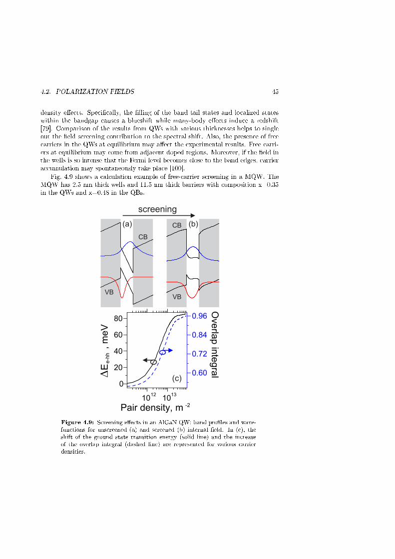
4.2. POLARIZATION FIELDS 45
density e�ects. Speci�cally, the �lling of the band tail states and localized stateswithin the bandgap causes a blueshift while many-body e�ects induce a redshift[79]. Comparison of the results from QWs with various thicknesses helps to singleout the �eld screening contribution to the spectral shift. Also, the presence of freecarriers in the QWs at equilibrium may a�ect the experimental results. Free carri-ers at equilibrium may come from adjacent doped regions. Moreover, if the �eld inthe wells is so intense that the Fermi level becomes close to the band edges, carrieraccumulation may spontaneously take place [100].
Fig. 4.9 shows a calculation example of free-carrier screening in a MQW. TheMQW has 2.5 nm thick wells and 11.5 nm thick barriers with composition x=0.35in the QWs and x=0.48 in the QBs.
CB
VBVB
CB
screening
1012
1013
0
20
40
60
80
Pair density, m -2
DE
e-h
h,
me
V
0.60
0.72
0.84
0.96
Ove
rlap
inte
gra
l
(c)
(a) (b)
Figure 4.9: Screening e�ects in an AlGaN QW: band pro�les and wave-functions for unscreened (a) and screened (b) internal �eld. In (c), theshift of the ground state transition energy (solid line) and the increaseof the overlap integral (dashed line) are represented for various carrierdensities.
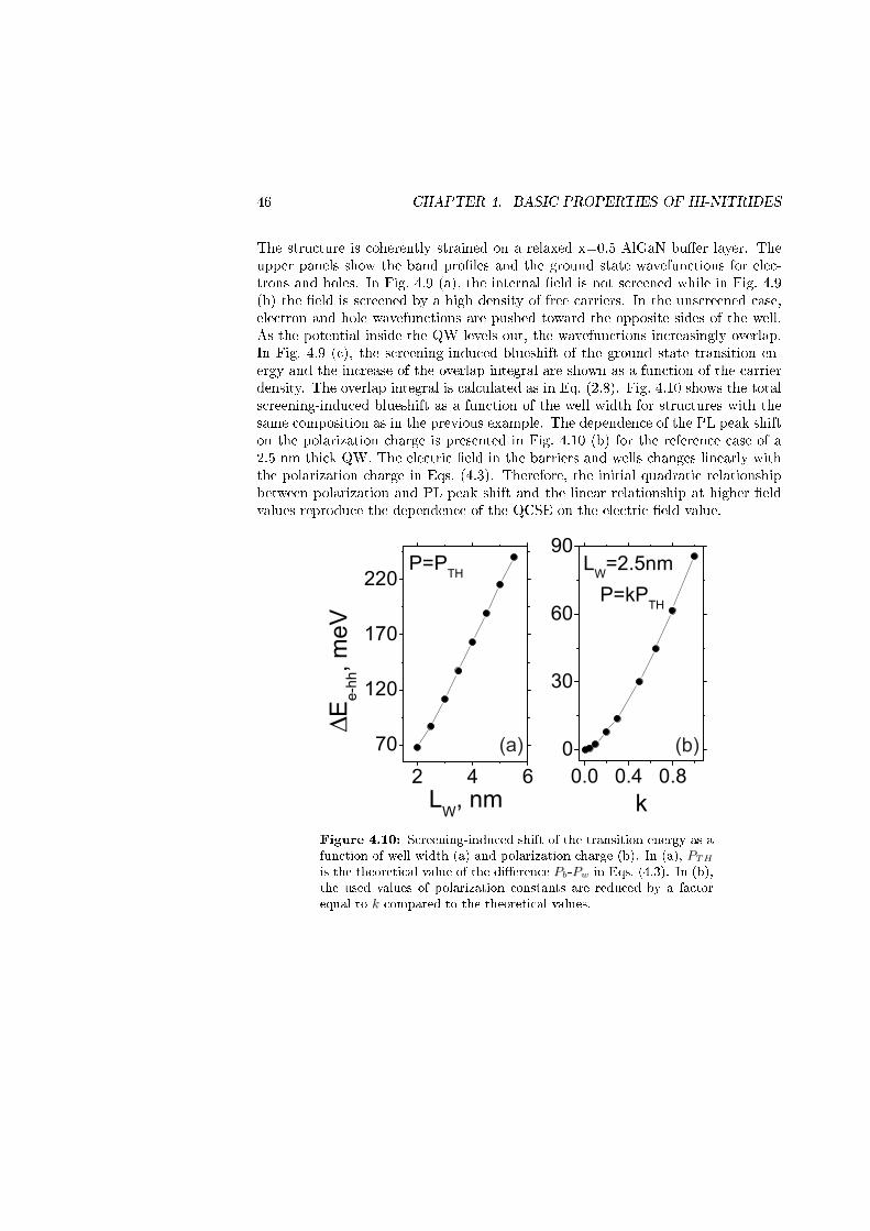
46 CHAPTER 4. BASIC PROPERTIES OF III-NITRIDES
The structure is coherently strained on a relaxed x=0.5 AlGaN bu�er layer. Theupper panels show the band pro�les and the ground state wavefunctions for elec-trons and holes. In Fig. 4.9 (a), the internal �eld is not screened while in Fig. 4.9(b) the �eld is screened by a high density of free carriers. In the unscreened case,electron and hole wavefunctions are pushed toward the opposite sides of the well.As the potential inside the QW levels out, the wavefunctions increasingly overlap.In Fig. 4.9 (c), the screening-induced blueshift of the ground state transition en-ergy and the increase of the overlap integral are shown as a function of the carrierdensity. The overlap integral is calculated as in Eq. (2.8). Fig. 4.10 shows the totalscreening-induced blueshift as a function of the well width for structures with thesame composition as in the previous example. The dependence of the PL peak shifton the polarization charge is presented in Fig. 4.10 (b) for the reference case of a2.5 nm thick QW. The electric �eld in the barriers and wells changes linearly withthe polarization charge in Eqs. (4.3). Therefore, the initial quadratic relationshipbetween polarization and PL peak shift and the linear relationship at higher �eldvalues reproduce the dependence of the QCSE on the electric �eld value.
2 4 6
70
120
170
220
DE
e-h
h, m
eV
LW
, nm
P=PTH
0.0 0.4 0.8
0
30
60
90
k
LW
=2.5nm
P=kPTH
(a) (b)
Figure 4.10: Screening-induced shift of the transition energy as afunction of well width (a) and polarization charge (b). In (a), PTHis the theoretical value of the di�erence Pb-Pw in Eqs. (4.3). In (b),the used values of polarization constants are reduced by a factorequal to k compared to the theoretical values.
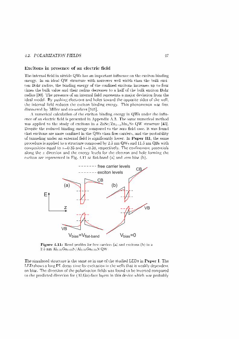
4.2. POLARIZATION FIELDS 47
Excitons in presence of an electric �eld
The internal �eld in nitride QWs has an important in�uence on the exciton bindingenergy. In an ideal QW structure with narrower well width than the bulk exci-ton Bohr radius, the binding energy of the con�ned excitons increases up to fourtimes the bulk value and their radius decreases to a half of the bulk exciton Bohrradius [30]. The presence of an internal �eld represents a major deviation from theideal model. By pushing electrons and holes toward the opposite sides of the well,the internal �eld reduces the exciton binding energy. This phenomenon was �rstdiscovered by Miller and co-workers [101].
A numerical calculation of the exciton binding energy in QWs under the in�u-ence of an electric �eld is presented in Appendix A.3. The same numerical methodwas applied to the study of excitons in a ZnSe/Zn1−xMnxSe QW structure [45].Despite the reduced binding energy compared to the zero �eld case, it was foundthat excitons are more con�ned in the QWs than free carriers, and the probabilityof tunneling under an external �eld is signi�cantly lower. In Paper III, the sameprocedure is applied to a structure composed by 2.5 nm QWs and 11.5 nm QBs withcomposition equal to x=0.35 and x=0.50, respectively. The con�nement potentialsalong the z direction and the energy levels for the electron and hole forming theexciton are represented in Fig. 4.11 at �at-band (a) and zero bias (b).
(a) (b)
V =0bias
free carrier levels
exciton levels
V =Vbias flat-band
z
E
CB
VB
VB
CB
Figure 4.11: Band pro�les for free carriers (a) and excitons (b) in a2.5 nm Al0.35Ga0.65N/Al0.50Ga0.50N QW.
The simulated structure is the same as in one of the studied LEDs in Paper I. TheLED shows a long PL decay time for excitation in the wells that is weakly dependenton bias. The direction of the polarization �elds was found to be inverted comparedto the predicted direction for (Al,Ga)-face layers in this device which was probably
48 CHAPTER 4. BASIC PROPERTIES OF III-NITRIDES
composed by N-face layers. The calculated tunneling- and thermionic emission-limited lifetimes as in Eqs. (2.20) and (2.21) in the free-carrier model are muchshorter than the measured PL decay time. Following Ref. [45], the calculationsin Paper III show that electron-hole Coulomb interaction enhances the carriercon�nement within the wells and reduces the probability of carrier escape from thewells. As a consequence, the obtained tunneling- and thermionic emission-limitedlifetimes in the exciton recombination model are comparable with the measuredPL decay time. Another possible explanation for the low tunneling and thermionicemission may be free carrier and/or exciton con�nement in potential minima. Thepresence of potential �uctuations in AlGaN QWs is discussed in Section 5.4.
Chapter 5
AlGaN-based light-emitting diodes
Beside the fundamental properties of the AlGaN alloys that have been presentedin the previous chapter, there are several other important aspects originating fromthe typical material growth and processing techniques. This chapter treats thetechnology, the structure and some issues related to the performance and reliabilityof deep-UV LEDs.
5.1 AlGaN epitaxial growth
The studied devices in this thesis were grown by the migration-enhanced metalor-ganic chemical vapor deposition (MEMOCVD). The MEMOCVD is a modi�edversion of the metalorganic vapor phase epitaxy (MOVPE) that was speci�callyintroduced to enhance the crystal quality of the AlGaN layers. In this section, anintroduction to the MOVPE and MEMOCVD growth of AlGaN layers on sapphireare given, as described in Ref. [71]. The description is not intended to be compre-hensive but only to highlight a few critical steps in the manufacturing of deep-UVlight-emitting devices.
All the commercially available devices and the vast majority of the researchprototypes are grown on lattice mismatched sapphire substrates [13, 16]. The equi-librium melt growth of III-nitride single crystals is complicated by the high equilib-rium nitrogen pressure on the binary III-nitrides at their melting temperature [102](see Appendix A.1). This determines the scarce availability of native substrateson the market to date. Sapphire substrates are widely available with good qualityand relatively low cost. Moreover, sapphire exhibits hexagonal symmetry and iscompatible with high temperature growth and ammonia environment.
MOVPE is usually employed for the growth of III-nitride-based devices becauseit allows the creation of abrupt interfaces and supplies a su�ciently high growthrate. N and group-III atoms are brought close to the growing surface as part of
49

50 CHAPTER 5. ALGAN-BASED LIGHT-EMITTING DIODES
larger precursor compounds: ammonia for N, trimethylgallium for gallium (Ga),trimethylalluminum for Al. Molecular hydrogen and nitrogen are used as carriergases. For the growth of doped layers, bis(cyclopentadienyl)magnesium and silaneare also �own into the chamber. The deposition occurs via pyrolysis of the precur-sors on the heated surface.
Among the substrate preparation steps, the exposure to ammonia at 600 C◦,called nitridation, is critical to �x the (Al,Ga)-face polarity of the following layers[103]. One of the major breakthrough in the III-nitride technology was the in-troduction of the nucleation layer (NL) by Amano in 1986 [4], which resulted in adrastic reduction of the dislocation density. This growth step consists in the deposi-tion of a thin (∼ 50 nm) GaN or AlN amorphous layer at low temperature followedby a temperature ramp-up. At high temperatures, the NL assumes a columnarstructure [104]. The columns are tilted and twisted with respect to each other toaccommodate the lattice mismatch with the substrate and provide a high nucleationdensity for the following high temperature growth. Initially, nearly dislocation-freetrapezoid III-nitride crystals grow on the top of the columns and eventually coales-cence. The boundaries of coalescence are likely to be the most defect-rich regionsof the epilayer. The TD density decreases with thickness [105] due to dislocationself-annealing. Although the NL is still widely employed for the growth of AlN, thenecessity of a NL in the AlN growth on sapphire is currently under debate [106]as good quality AlN layers were directly grown on sapphire at high temperatures[107]. The growth temperature for AlGaN epitaxial layers is higher than the onefor GaN, typically between 1100 ◦C and 1220 ◦C [108].
The choice of the growth parameters, particularly growth temperature, totalprecursor �ow rate and III/V precursor �ow ratio, is dictated by several trade-o�s.The thermal stability of ammonia requires high substrate temperatures to dissociatethe molecule. Besides, high growth temperatures are needed to mobilize TDs andpromote their self-annealing during growth. However, the high nitrogen vaporpressure over the III-nitrides at the growth temperature leads to the inevitablenitrogen loss from the �lm. Therefore, N vacancies (VN ) and voids may format high growth temperatures [71]. Besides, the mismatch of thermal expansioncoe�cient for sapphire and the III-nitrides induces a high mechanical stress whencooling from high temperatures that may cause the cracking of the layer. Finally,the growth temperature and the III/V precursor �ow ratio in�uence the uniformityof incorporation of the metallic species on the surface via their di�usion length.The di�usion length of the adatoms on the surface quanti�es the average lengththat the adatoms cover on the surface between adsorption and incorporation intothe crystal or desorption. The limited di�usion length of Al adatoms is particularlycritical for the growth of high quality AlGaN layers. Ideally, the growth proceedslayer by layer. For this to happen, the di�usion length of the metallic adatoms mustbe su�cient to reach the boundaries of the lateral expansion of the growing layer.The di�usion length of the group-III adatoms can be enhanced to some extent byincreasing the growth temperature, adjusting the total precursor �ow rate and theIII/V �ow ratio. Usually, slight Ga rich conditions, for which the growth rate is
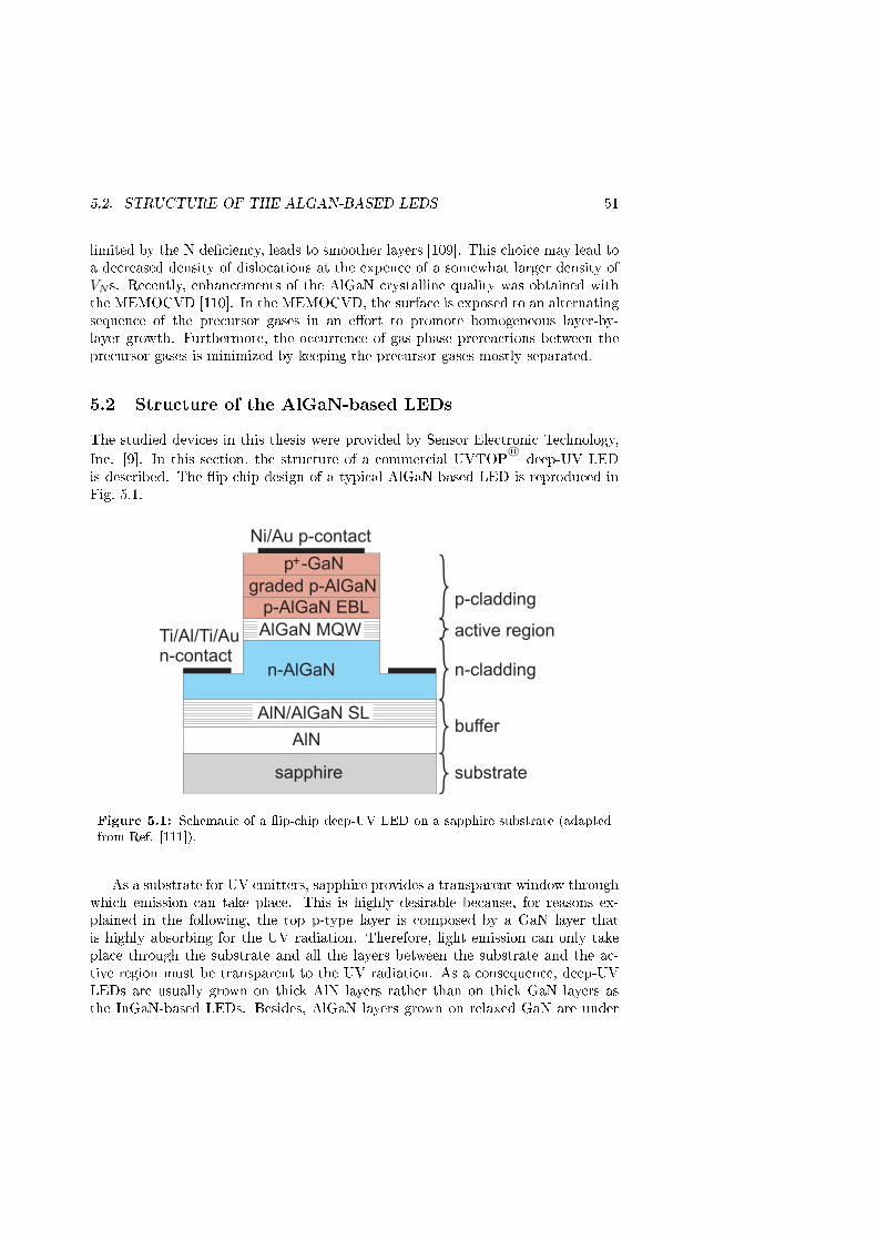
5.2. STRUCTURE OF THE ALGAN-BASED LEDS 51
limited by the N de�ciency, leads to smoother layers [109]. This choice may lead toa decreased density of dislocations at the expence of a somewhat larger density ofVN s. Recently, enhancements of the AlGaN crystalline quality was obtained withthe MEMOCVD [110]. In the MEMOCVD, the surface is exposed to an alternatingsequence of the precursor gases in an e�ort to promote homogeneous layer-by-layer growth. Furthermore, the occurrence of gas-phase prereactions between theprecursor gases is minimized by keeping the precursor gases mostly separated.
5.2 Structure of the AlGaN-based LEDs
The studied devices in this thesis were provided by Sensor Electronic Technology,Inc. [9]. In this section, the structure of a commercial UVTOP
R©deep-UV LED
is described. The �ip-chip design of a typical AlGaN-based LED is reproduced inFig. 5.1.
sapphire
AlN
AlN/AlGaN SL
AlGaN MQW
p-AlGaN EBL
+p -GaN
n-AlGaN
buffer
n-cladding
active region
p-cladding
substrate
Ni/Au p-contact
Ti/Al/Ti/Au n-contact
graded p-AlGaN
Figure 5.1: Schematic of a �ip-chip deep-UV LED on a sapphire substrate (adaptedfrom Ref. [111]).
As a substrate for UV emitters, sapphire provides a transparent window throughwhich emission can take place. This is highly desirable because, for reasons ex-plained in the following, the top p-type layer is composed by a GaN layer thatis highly absorbing for the UV radiation. Therefore, light emission can only takeplace through the substrate and all the layers between the substrate and the ac-tive region must be transparent to the UV radiation. As a consequence, deep-UVLEDs are usually grown on thick AlN layers rather than on thick GaN layers asthe InGaN-based LEDs. Besides, AlGaN layers grown on relaxed GaN are under
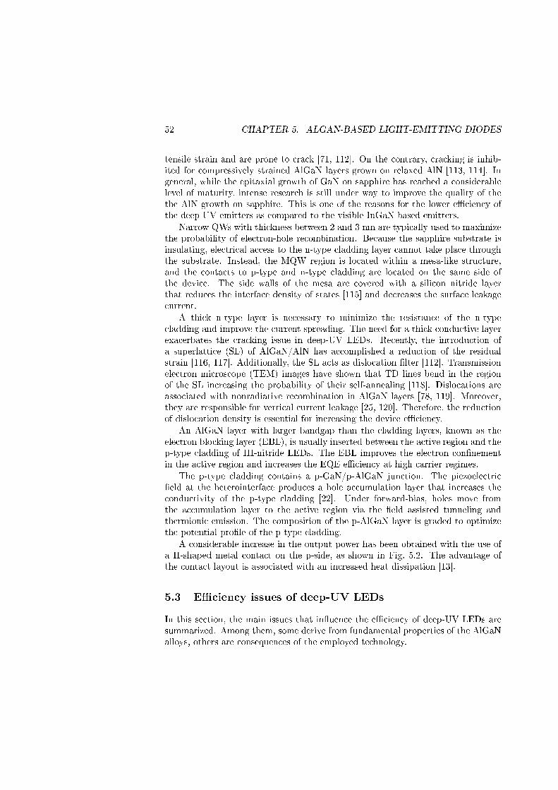
52 CHAPTER 5. ALGAN-BASED LIGHT-EMITTING DIODES
tensile strain and are prone to crack [71, 112]. On the contrary, cracking is inhib-ited for compressively strained AlGaN layers grown on relaxed AlN [113, 114]. Ingeneral, while the epitaxial growth of GaN on sapphire has reached a considerablelevel of maturity, intense research is still under way to improve the quality of thethe AlN growth on sapphire. This is one of the reasons for the lower e�ciency ofthe deep-UV emitters as compared to the visible InGaN-based emitters.
Narrow QWs with thickness between 2 and 3 nm are typically used to maximizethe probability of electron-hole recombination. Because the sapphire substrate isinsulating, electrical access to the n-type cladding layer cannot take place throughthe substrate. Instead, the MQW region is located within a mesa-like structure,and the contacts to p-type and n-type cladding are located on the same side ofthe device. The side walls of the mesa are covered with a silicon nitride layerthat reduces the interface density of states [115] and decreases the surface leakagecurrent.
A thick n-type layer is necessary to minimize the resistance of the n-typecladding and improve the current spreading. The need for a thick conductive layerexacerbates the cracking issue in deep-UV LEDs. Recently, the introduction ofa superlattice (SL) of AlGaN/AlN has accomplished a reduction of the residualstrain [116, 117]. Additionally, the SL acts as dislocation �lter [112]. Transmissionelectron microscope (TEM) images have shown that TD lines bend in the regionof the SL increasing the probability of their self-annealing [118]. Dislocations areassociated with nonradiative recombination in AlGaN layers [78, 119]. Moreover,they are responsible for vertical current leakage [25, 120]. Therefore, the reductionof dislocation density is essential for increasing the device e�ciency.
An AlGaN layer with larger bandgap than the cladding layers, known as theelectron blocking layer (EBL), is usually inserted between the active region and thep-type cladding of III-nitride LEDs. The EBL improves the electron con�nementin the active region and increases the EQE e�ciency at high carrier regimes.
The p-type cladding contains a p-GaN/p-AlGaN junction. The piezoelectric�eld at the heterointerface produces a hole accumulation layer that increases theconductivity of the p-type cladding [22]. Under forward-bias, holes move fromthe accumulation layer to the active region via the �eld assisted tunneling andthermionic emission. The composition of the p-AlGaN layer is graded to optimizethe potential pro�le of the p-type cladding.
A considerable increase in the output power has been obtained with the use ofa H-shaped metal contact on the p-side, as shown in Fig. 5.2. The advantage ofthe contact layout is associated with an increased heat dissipation [13].
5.3 E�ciency issues of deep-UV LEDs
In this section, the main issues that in�uence the e�ciency of deep-UV LEDs aresummarized. Among them, some derive from fundamental properties of the AlGaNalloys, others are consequences of the employed technology.

5.3. EFFICIENCY ISSUES OF DEEP-UV LEDS 53
sapphire
p-contact
Figure 5.2: H-shaped pad layout of deep-UV LEDs. Theright-hand side of the �gure shows a micrograph of the EL froma device emitting at 310 nm. The observed shape reproducesthe layout of the top p-type contact.
(i) The polarization �elds in devices that are grown on polar surfaces separatethe opposite sign carriers in the wells decreasing the probability of radiativerecombination. This negative e�ect can be overcome to large extent by usingthin QWs. However the polarization �elds impact the wall-plug e�ciency inother ways. The band pro�les in CB and VB across a typical LED structureare shown in Fig. 5.3 (the parameters of the simulated structure are the sameas for the calculations presented in Fig. 4.10). The polarization sheet chargeat the interface between layers produces potential barriers that impede thecarrier transport [20, 21]. The presence of polarization-induced barriers wasassociated with the high ideality factor that is usually measured in III-nitride-based LEDs [20].
(ii) The low conductivity of p-type and n-type cladding layers is a major issue thata�ects the wall-plug e�ciency and durability of deep-UV LEDs. The conduc-tivity of AlGaN layers is impaired by compensating and scattering centers [8],thus, high crystal quality layers are of primary importance. However, fun-damental obstacles remain to the achievement of highly conductive AlGaNlayers. At variance with unintentionally doped GaN layers that are usually n-type, unintentionally doped AlxGa1−xN �lms with x>0.4 are highly resistive.Although the n- and p-type doping of GaN and InGaN are well established,the successful doping of AlGaN is much more complicated. The commonlyused dopant impurities are silicon (Si) and magnesium (Mg) that introducedonor and acceptor states, respectively. With increasing Al composition, theconductivity of epilayers for both doping types rapidly decreases. This is dueto the continuous increase of the donor and acceptor ionization energies. Theactivation energy of Si increases linearly from 20 meV in GaN to 320 meV inAlN [121]. These values correspond to 0.8kBT and 12.5kBT, respectively, atroom temperature. The activation energy of Mg is even higher. It increasesalmost linearly from 160 meV in GaN to 500 meV in AlN [122], correspondingto 6.3kBT and 19.5kBT at room temperature. So far, the p-GaN/p-AlGaN

54 CHAPTER 5. ALGAN-BASED LIGHT-EMITTING DIODES
0 50 100 150
0
1
4
5
ban
d p
rofile
, eV
z, nm
active region EBL
gra
ded r
egio
n
n-A
lGaN
p-G
aN
e
h
Figure 5.3: CB (blue) and VB (red) pro�les for a deep-UV MQWLED near �at-band condition. The pro�les are calculated solving thePoisson equation in the approximation I≈0. The electron and holecurrents are indicated with dotted blue and red lines, respectively.The potential barriers that impede the carrier �ow are circled in black.
heterointerface and the SL doping [8] approaches have only partially solvedthe problem of the low p-type conductivity.
(iii) As it was mentioned previously, signi�cant emission in the TM polarizationmay occur in structures with high Al molar fraction in the active region.Although there is still little experimental evidence, it seems that this mecha-nism takes place at very high Al molar fractions. Therefore, it is unlikely thatTM polarized emission in�uences signi�cantly the e�ciency of commerciallyavailable devices.
(iv) The e�ciency of InGaN-based LEDs decreases under high carrier injection, aphenomenon known as e�ciency droop. The origin of the e�ciency droop isstill under debate. Auger recombination is one of the explanations that havebeen put forward. The probability of Auger recombination in direct bandgapsemiconductors decreases strongly with increasing bandgap energy [123]. Forthe III-V semiconductors other than the III nitrides, an exponentially decreas-ing trend is recognizable in spite of large uncertainties. The extrapolation ofthe trend for GaN would lead to an upper bound of 10−34 cm6s−1. This valueagrees with �rst principle calculations for intraband Auger recombination.However, experimental values are much larger, usually in the range between1×10−31 and 3×10⁻³⁰ cm6s−1 as measured in InGaN-based heterostructures.Re�ned models were employed to explain the experimental data. It was found
5.3. EFFICIENCY ISSUES OF DEEP-UV LEDS 55
that interband Auger recombination can occur in green-emitting InGaN alloys[124]. However, this process is not likely to occur in AlGaN alloys because ofthe di�erent energy gaps between the electronic bands. In a recent publica-tion, values closer to the experimental ones were calculated including indirectAuger processes that involve electron-phonon coupling and alloy scattering[125]. The e�ciency droop in AlGaN-based layers occurs at much higher cur-rent densities than in InGaN-based LEDs [89, 126]. This may hint to a smallervalue of Auger coe�cients in AlGaN. In any case, the e�ect of Auger recom-bination can be neglected from the interpretation of our experimental data.Although Auger recombination may limit the e�ciency of high-brightness de-vices in the future, it appears to be of secondary importance in the perfor-mance of commercial low-current-density devices to date.
(v) The electron leakage in the p-cladding at high current densities o�ers an al-ternative explanation for the e�ciency droop in GaN-based LEDs [89]. Thisphenomenon is common to III-nitride-based LEDs because of the larger dif-fusion constant of electrons compared with holes in III-V semiconductors [2].Moreover, leakage is enhanced at high current densities by band �lling in theactive region and device self-heating. Electron leakage in the p-type claddingwas associated with a broad red-shifted band in the EL spectra. The bandis originated from the electron recombination with a deep level in the p-typecladding [127, 128]. The EBL has proven to quench the red-shifted emissionband and increase the e�ciency at low to medium carrier regimes althoughthe leakage still limits the e�ciency at high current densities [89].
(vi) The density of dislocations was determined to be of primary importance inAlGaN-based devices. Experiments have shown that the IQE of MQW struc-tures can be increased from 4% to 64% in a wide range of compositions byreducing the dislocation density [129]. The strong in�uence of the crystalquality on the IQE of the devices was also con�rmed by the increased lu-minescence decay time in high quality layers grown by MEMOCVD [130].Although there is direct evidence that dislocations act as nonradiative re-combination centers in III-nitrides, the speci�c carrier trapping mechanismmay change with sample composition and doping. The study in Paper IV
suggests that dislocations may be e�cient nonradiative recombination centerswhen they are decorated with point defects. Furthermore, the in�uence ofpotential �uctuations around dislocations is discussed in Section 5.4.
(vii) The EQE of �ip-chip devices is severely limited by the internal re�ection atthe sapphire substrate interfaces. The light extraction e�ciency for �ip-chipGaN-based LEDs emitting through the sapphire substrate is around 23% [131].Moreover, strong absorption in the p-GaN layer does not allow recovering theemitted photons on the side of the p-type contact. However, di�erent designshave been developed to alleviate these problems in visible and near-UV LEDs,

56 CHAPTER 5. ALGAN-BASED LIGHT-EMITTING DIODES
such as the use of patterned substrates [132]. Similar solutions may eventuallybe deployed in deep-UV LEDs as well.
(viii) The comparison between the EQE under pulsed and continuous operationmodes reveals that device self-heating is a serious problem in AlGaN devices[13]. Self-heating is due to the low conductivity of the doped cladding regionsand the low thermal conductivity of sapphire. The reduction of the radiativerecombination at increasing temperatures derives from the intrinsic temper-ature dependence of the bimolecular radiative recombination coe�cient andthe reduced carrier con�nement in the active region.
5.4 Crystal inhomogeneities
Three types of inhomogeneities are commonly encountered in III-nitride epitaxiallayers: compositional inhomogeneity [60], strain inhomogeneity [133] and extendeddefects [134, 135]. Additionally, �uctuations of the well thickness may occur inQW structures [136, 137]. The simultaneous presence of di�erent kinds of inhomo-geneities is often correlated, as Fig. 5.4 schematically portrays.
compositional fluctuations
strain inhomogeneity
dislocations
adatom mobility mismatch
diffusion through dislocations
misorientation of columns
QW thickness variations
Figure 5.4: Inhomogeneities in III-nitride epitaxial layers andtheir interplay.
As outlined in Section 5.1, the growth of III-nitride layers on lattice mismatchedsubstrates typically proceeds via coalescence of separated trapezoid crystals withdi�erent orientations [104, 138]. The misorientation among the crystals is par-tially accommodated by the formation of dislocations at the boundaries of coales-cence. Nonetheless, an inhomogeneous strain �eld remains around the dislocations
5.4. CRYSTAL INHOMOGENEITIES 57
[139, 140], as observed in TEM measurements. The di�erence in mobility betweenthe group-III adatoms is responsible for the formation of domains with di�erentcompositions during the growth of AlGaN epilayers [141]. Di�erences of latticeconstant within these domains give rise to an additional component of inhomoge-neous strain. The formation of inhomogeneous domains is aided by dislocationsand inhomogeneous strain distribution as well. In fact, the atoms in the latticemay preferentially di�use through the dislocation cores [142] during growth anddevice aging. Furthermore, the adatoms locally redistribute on the growing surfaceas to minimize the strain in the layer [133]. Therefore, compositional changes mayoccur around dislocations, where the strain is partially relaxed. Lastly, TDs inQWs were linked with variations of the well thickness that result in �uctuations ofthe con�nement potentials for electrons and holes [137].
Inhomogeneities have a profound in�uence on the electrical and luminescenceproperties of III-nitride layers. In general, all inhomogeneities of the crystal struc-ture constitute a source of carrier scattering and impair the carrier mobility. Con-cerning the luminescence properties, the presence of inhomogeneities locally shiftsthe peak wavelength. For example, Fig. 5.5 shows an estimation of the e�ect ofcompositional variations, monolayer thickness variations and strain relaxation onthe ground state transition energy of an AlGaN MQW at low carrier densities.
-0.10 -0.05 0.00 0.05
-0.4
-0.3
-0.2
-0.1
0.0
0.1
0.2
strain rel. rel. & - monol.
DE
e-h
h,
eV
Dx, %
D composition + monolayer - monolayer
Lw=2.5 nm
xw=0.35
Lb=11.5 nm
xb=0.48
xc=0.5
Figure 5.5: Bandgap variation in a 2.5 nm QW induced by monolayervariations and strain relaxation. The bandgap values are calculatedsolving the Schrödinger equation in the e�ective mass approximation.The details of the calculation and the used material parameters aresummarized in Appendix A.1 and A.2.
58 CHAPTER 5. ALGAN-BASED LIGHT-EMITTING DIODES
The considered structure is composed by �ve 2.5 nm thick Al0.35Ga0.65N QWsand 11.5 nm Al0.48Ga0.52N QBs on a relaxed Al0.5Ga0.5N bu�er layer. Otherinhomogeneity-related e�ects are spectral broadening and nonradiative recombina-tion at dislocations.
Summarizing, the spectral width, peak position and luminescence e�ciency de-pend in di�erent proportions on the kind of inhomogeneity and the interplay be-tween them. The rest of this chapter reviews several kinds of compositional inhomo-geneities that are found in III-nitride layers with particular emphasis on the alloy�uctuations. Firstly, the issue of alloy �uctuations in epitaxial layers and QWs isbrie�y reviewed in the case of InGaN alloys, that have been more thoroughly stud-ied than AlGaN alloys. The obtained results provide insight in the AlGaN case.The available results for the AlGaN alloys follow after that.
Compositional inhomogeneities in InGaN
The luminescence e�ciency of InGaN layers strongly depends on the relationshipbetween dislocations and alloy �uctuations. High luminous e�ciency is obtainedin samples where the minority carrier di�usion length is smaller than the averagedislocation distance. This suggests that carrier localization in potential minimacaused by compositional �uctuations has the benign e�ect of con�ning the carriersaway from the detrimental dislocations in blue-emitting InGaN layers [23, 85]. Ac-tually, SNOM measurements in QW layers combined with high-resolution atomicforce microscope scans revealed the presence of regions emitting at red-shifted wave-lengths. The size of the regions was comparable with the defect distance [135] andtheir origin was associated with compositional inhomogeneities. The measurementswere found to be well-described by the presence of a miscibility gap [143].
In another work, TEM measurements revealed that the QW thickness is smalleraround the TDs that are connected to V-pits in blue-emitting InGaN QW structures[137]. A smaller QW thickness around the TDs determines a larger bandgap. Thus,a potential barrier around the TD cores isolates the carriers from the TDs.
The presence of dislocations in�uences the compositional homogeneity as well.In accumulation at the cores of TDs was observed in CL measurements on QWstructures [144]. The In excess at the TD cores may leave In-poor regions aroundthe TDs. NF measurements on blue-emitting InGaN layers in another study [145]con�rmed that deep exciton localization occurs in the In-rich regions at the sites ofTDs, where the bandgap is narrower. Furthermore, the presence of local potentialmaxima surrounding the TDs was observed. The local potential maxima probablycorrespond to the In-poor areas around the TD cores, and act as potential barriersfor the carriers outside the defective regions. Such potential barriers were notobserved around the TDs in green-emitting InGaN layers. In this case, the NFmeasurements in Ref. [146] revealed that the carriers are free to di�use to the TDcores, where they recombine nonradiatively. Therefore, the relationship betweenpotential �uctuations and TDs seems to change with the sample preparation andcomposition.

5.4. CRYSTAL INHOMOGENEITIES 59
Compositional inhomogeneities in AlGaN
Contrary to InGaN alloys, AlGaN alloys do not have a miscibility gap at practicalgrowth temperatures [147]. Because the mis�t between AlN and GaN is only 2.5%,one would expect a stable growth of AlGaN with a good control of the composition.However, several kinds of compositional inhomogeneities are commonly observed:random alloy disorder, alloy �uctuations, alloy segregation and ordering.
Randomly distributed alloy systems always present a certain degree of disorderat the scale of the lattice cell as a result of the statistical occupancy of the latticesites [148]. Alloy �uctuations usually refer to average variations of the alloy com-position on a larger scale than the lattice cell. Segregation is the extreme situationfor which one of the atoms or binary constituents of an alloy condensates within aregion of the crystal. Alloy �uctuations and segregation usually occur within irreg-ular volumes that have limited lateral size and do not present internal structure.On the other hand, ordering refers to the formation of domains containing a SL ofspontaneous QWs along the growth direction. Ordering sometimes occurs withinsmall areas of the sample [149], but it can also extend over the whole sample surface[150].
In AlGaN, the degree of alloy disorder has been determined from the broadeningof the exciton linewidth [151]. Regarding the ordering, TEM measurements haverevealed the presence of spontaneous QWs along the c-axis [149, 152, 153] withina wide range of compositions. Ordering occurs because there are several orderedcon�gurations of atoms with formation energies that are close to each other andto the perfectly random con�guration [147]. The formation of ordered structuresseems to be favored by the kinetics of the adatoms on the surface in the layer-by-layer growth mode [149]. Ordering was identi�ed as the cause of the uncertainty onthe value of the bowing parameter. Concerning the segregation in AlGaN alloys,Al segregation has been observed in TEM measurements around TDs in MOVPEgrown samples [154]. Similarly to In segregation in InGaN layers, the Al surpluscomes from Al-depleted regions that were observed within a few nanometers fromthe dislocation lines. Alloy �uctuations in AlGaN are treated in more detail in thefollowing subsection.
Alloy �uctuations in AlGaN
Several luminescence experiments reveal the presence of alloy �uctuations in AlGaNlayers. Carrier localization in domains with di�erent compositions is evidenced bythe wavelength shift between the peak of the absorption and emission spectra -the Stockes' shift. While the emission at low carrier densities is dominated by theexciton recombination in the potential minima, the absorption threshold occurs atthe energy for which the density of states has a steep rise. Additionally, the sameconclusion can be derived from the the temperature dependence of the emissionpeak wavelength [155]. The thermally activated exciton hopping between local

60 CHAPTER 5. ALGAN-BASED LIGHT-EMITTING DIODES
potential minima determines a characteristic �S� shape for the peak wavelengthdependence on the temperature [156].
Interestingly, the measured PL decay time in AlGaN layers at 10 K increasesas the Al mole fraction is increased [24]. This behavior is theoretically explainedby the increase of the exciton radiative lifetime for increasing localization depths.Therefore, the presence of deeper localization potentials in layers with higher Almolar fraction has been suggested. Additionally, the room temperature lifetime ofthe nonequilibrium carriers was found to be limited by the carrier di�usion to thedislocations, where nonradiative recombination takes place [78]. These results seemto corroborate a similar role of potential �uctuations in Al-rich AlGaN layers as inblue-emitting InGaN layers.
In Paper VI, the presence of potential minima in AlGaN-based QWs was de-duced from DTPP measurements. The DTPP traces that were measured at di�er-ent photon energies are shown in Fig. 5.6.
0 50 100 150 200
282 nm
276 nm
272 nm
270 nm
DT (
arb
. u
nits
)
Delay time (ps)
265 nm
excitation in localized states in the QWs
excitation in extended states in the QWs
excitation in the QBs
Figure 5.6: DTPP traces from 3.3 nm thick Al0.35Ga0.65N QWs separatedby 11.5 nm thick Al0.49Ga0.51N QBs.
At intermediate photon energies (red curves), carriers are excited in the QW ex-tended states above the bandgap and the induced transmission decays with a char-acteristic time of 80-150 ps. At lower photon energies (black curves), carriers aredirectly excited in the localized states with a longer lifetime, and the shape of thedi�erential transmission transients becomes steplike with a very long decay time.
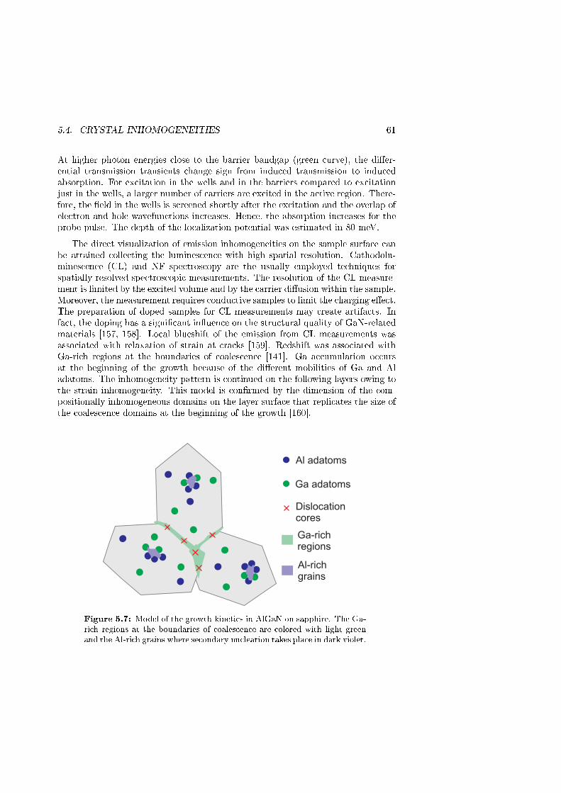
5.4. CRYSTAL INHOMOGENEITIES 61
At higher photon energies close to the barrier bandgap (green curve), the di�er-ential transmission transients change sign from induced transmission to inducedabsorption. For excitation in the wells and in the barriers compared to excitationjust in the wells, a larger number of carriers are excited in the active region. There-fore, the �eld in the wells is screened shortly after the excitation and the overlap ofelectron and hole wavefunctions increases. Hence, the absorption increases for theprobe pulse. The depth of the localization potential was estimated in 80 meV.
The direct visualization of emission inhomogeneities on the sample surface canbe attained collecting the luminescence with high spatial resolution. Cathodolu-minescence (CL) and NF spectroscopy are the usually employed techniques forspatially resolved spectroscopic measurements. The resolution of the CL measure-ment is limited by the excited volume and by the carrier di�usion within the sample.Moreover, the measurement requires conductive samples to limit the charging e�ect.The preparation of doped samples for CL measurements may create artifacts. Infact, the doping has a signi�cant in�uence on the structural quality of GaN-relatedmaterials [157, 158]. Local blueshift of the emission from CL measurements wasassociated with relaxation of strain at cracks [159]. Redshift was associated withGa-rich regions at the boundaries of coalescence [141]. Ga accumulation occursat the beginning of the growth because of the di�erent mobilities of Ga and Aladatoms. The inhomogeneity pattern is continued on the following layers owing tothe strain inhomogeneity. This model is con�rmed by the dimension of the com-positionally inhomogeneous domains on the layer surface that replicates the size ofthe coalescence domains at the beginning of the growth [160].
Al adatoms
Ga adatoms
Dislocation cores
Al-rich grains
Ga-rich regions
Figure 5.7: Model of the growth kinetics in AlGaN on sapphire. The Ga-rich regions at the boundaries of coalescence are colored with light greenand the Al-rich grains where secondary nucleation takes place in dark violet.

62 CHAPTER 5. ALGAN-BASED LIGHT-EMITTING DIODES
The same mechanisms that govern the formation of compositionally inhomoge-neous domains in AlGaN and InGaN alloys strongly a�ect the surface morphologyas well [133, 161]. Particularly in high Al molar fraction layers, the low mobility ofthe Al adatoms leads to secondary nucleation and increases the surface roughness[162]. The formation of compositionally inhomogeneous domains and secondarynucleation are schematically represented in Fig. 5.7.
So far, SNOM has found a limited application to the study of the homogeneityof AlGaN alloys [163]. This can be explained with the di�culties of using thistechnique in the UV range. On the other hand, NF measurements have someadvantages with respect CL measurements. In IC mode or collection mode, NFmeasurements are less a�ected by the carrier di�usion in the sample and do notrequire any speci�c sample preparation.
In Paper VIII, SNOM measurements have revealed distinctive di�erencesamong AlGaN layers with di�erent nominal compositions. In the SNOM measure-ments, the presence of localization on a larger spatial scale than the experimentresolution can be detected by means of the peak wavelength shift. If the inhomo-geneity occurs on a �ner scale, the spectral broadening provides an estimate of theaverage potential depth of the �ne compositional variations (see Section 2.3). Themeasurements have evidenced an interesting relationship between the redshift andthe spectral broadening as can be seen in the NF spectra in Fig. 5.8 (b).
A
B
4.0 4.2 4.4
NF in A
NF in B
FF
(b) NF and FF spectra(a) peak energy4.220
4.177
eV
energy, eV2 mm
ph. co
unt, a
.u.
Figure 5.8: NF peak energy map (a) from a 30% Al molar fraction epi-taxial layer. In (b), the FF spectrum and the NF spectra from di�erentpoints on the sample are compared.
This is probably due to the presence of a double scale localization potential [130]with �ne potential �uctuations within larger compositionally inhomogeneous do-mains. Fig. 5.9 shows a measurement on a sample with 42% Al molar fraction.The measurement evidences a positive correlation between the peak energy and thepeak intensity. The correlation suggests that, at least in some composition range,

5.5. LED AGING 63
enhanced nonradiative recombination takes place within the potential minima, sim-ilarly as in green-emitting InGaN layers.
(b) peak energy(a) peak intensity
2 mm
4.335
4.310
275.3
70.8
eV
arb
.units
2 mm
Figure 5.9: NF peak intensity map (a) and peak energy map (b) from a42% Al molar fraction epitaxial layer.
5.5 LED aging
The operation lifetime of commercial deep-UV LEDs is of the order of 5000 hoursfor devices emitting at λ>300 nm [13] at the recommended current of 20 mA.Much shorter operation lifetimes are measured at higher currents [17] or in devicesemitting at shorter wavelengths. These values are signi�cantly lower than theoperation lifetime of high-brightness InGaN-based LEDs of around 40000 hours[14]. A limited amount of work has been devoted to reliability studies of the sub-300 nm LEDs [26, 70, 164�166]. Two main failure scenarios, gradual and abrupt,have been identi�ed [70]. The abrupt failure was associated with the presence ofV-pits on the LED surface. V-pits occur at the surface termination of open-coreTDs that form leakage paths through the active region. The high current densityin the vicinity of these defects produces local overheating, atom migration from thecontacts and formation of local electric shorting of the p-n junction [70].
The gradual output power degradation was initially linked to the formation ofnonradiative recombination defects during degradation [166]. However, the compar-ison of the EL and PL from the active region has shown that no signi�cant increaseof the nonradiative recombination in the active region occurs after degradation [26].Alternatively, the formation of VN s in the p-cladding was proposed to explain thegradual device degradation. According this interpretation, the formation of VN sduring the device operation would be caused by electrons with high kinetic energythat traverse the junction under high current densities. Additionally, it has beenshown that the device self-heating strongly reduces the operation lifetime [17].

64 CHAPTER 5. ALGAN-BASED LIGHT-EMITTING DIODES
Regardless the actual aging process, the device operation lifetime is stronglydependent on the dislocation density. Laboratory prototypes grown on patternedsubstrates by the MEMOCVD technique present reduced dislocation density andlonger operation lifetime [167].
Paper V contains a NF study of a case of abrupt device failure. The resultsare summarized in Fig. 5.10.
Peak wavelength
x mm
280 300 320
280 300 320
Inte
ns
ity
,a
rb.u
nit
s
280 300 320
Wavelength, nm280 300 320
8.5
4.9
arb
.u.
13.5
6.5
arb
.u.
7.2
0.2
arb
.u.
3.1
0.1
arb
.u.
nm
286.0
284.5
nm
296.4
284.6
nm
302.0
285.0
nm
314.0
283.0
5m
m
5 mm
Intensity Spectra
Figure 5.10: Failure of a 285 nm deep-UV LED. The rows from topto bottom represent successive NF measurements. In every row, the �rstcolumn shows the spectrally integrated intensity, the second the peak wave-length and the third the spectra collected along a scan that is indicated bya dashed black line on the intensity maps.
Discrete regions with red-shifted emission and typical dimension of a few microme-ters were observed. The magnitude of the redshift was observed to increase duringaging and was explained with the migration of Al atoms out of the well region alongdislocations. As mentioned before, Al segregation has been previously measured

5.5. LED AGING 65
at TD cores [154], leaving Al-poor regions around them. Further atom migrationduring aging could produce high current paths through the active region. Intenseself-heating in the regions of high current density would induce a current run-awaymechanism.
The gradual device failure after DC current stress is studied in Paper VII. TheFF comparison of EL and PL con�rms that the active region is not signi�cantlydamaged during the aging process. The device deterioration seems to be related totwo phenomena: the emission of a wide, red-shifted band with respect to the mainpeak and the increase of conductivity at low reverse and forward bias.
Red-shifted emission band
The red-shifted emission band has been previously documented for AlGaN-basedLEDs emitting at 325 nm [168], 285 nm [169] and 270 nm [170]. In all of thesestudies, the peak has been attributed to the carrier recombination in the p-cladding.The well-documented electron leakage in the p-type cladding of III-nitride-basedLEDs [89] supports this interpretation. Di�erent types of transitions have beeninvoked to explain the red-shifted band, such as transitions between the CB andthe Mg acceptor level [169] and between the nitrogen vacancy donors V 3+
N s and theMg acceptors [122]. Furthermore, aging experiments in Ref. [170] have revealedthat the weight of the red-shifted band on the total emission spectrum increasesduring aging, as shown in Fig. 5.11. This result suggests the emergence of analternative recombination path during aging.
240 260 280 300 320 340
0.0
0.2
0.4
0.6
0.8
1.0
inte
nsity,
arb
.un
its
wavelength, nm
I≈10 mA
virgin
aged
Figure 5.11: EL from a 265 nm deep-UV LED before (solid line) andafter (dashed line) aging (reproduced from Ref. [170]).

66 CHAPTER 5. ALGAN-BASED LIGHT-EMITTING DIODES
In Paper VII, evidence is presented that indicates the origin of the red-shiftedband in transitions between the V 3+
N s and the VB. The donor-acceptor type re-combination can be excluded because the measured luminescence decay time of thered-shifted band is much shorter than the typical decay time for donor-acceptor pairtransitions [171]. The CB to the Mg-acceptor level transition can also be excludedbecause it would generate a red-shifted band in a di�erent spectral position. Also,the increased weight of the red-shifted emission band after aging suggests that thedensity of V 3+
N increases during aging.
Vertical conduction at extended defects
The analysis of the I-V curves in Paper VII evidences an increase of the conduc-tivity at low reverse and forward bias and a decrease at high forward bias. Anincrease of the tunneling conduction at TDs was proposed to explain the aging-induced conductivity increase. In general, the results of scanning current-voltagemeasurements support the mechanism of tunneling conduction around dislocations[25, 120]. GaN layers contain large densities of crystallographic defects, amongwhich TDs [172], nanopipes, inversion domains [173], and pyramidal planar defects[158, 174] can cross the whole epitaxial layer and hamper the electrical and opticalproperties. There is still a controversy around the electrical and optical activity ofthe di�erent kinds of defects [172, 175]. However, open-core screw dislocations havebeen indicated as the most likely responsible for the leakage current through theactive region of III-nitride-based LEDs [25, 120]. Screw dislocations in GaN existas full-core screw dislocations, screw dislocations with a narrow opening or in theform of nanopipes, whereas the edge dislocations have �lled cores [172]. Whetherthe screw dislocation cores in GaN are �lled, depends on the growth conditions anddoping. Due to the large stress �eld near dislocations, point defects, complexes, andimpurities can be trapped at dislocations rendering them electrically active [176].Moreover, coreless screw dislocations have been reported to start from V-shapedindentations, the density of which increases with higher concentrations of impuritiesor dopants [158, 174]. Therefore, there seems to be a connection between getteringof impurity at dislocation cores and formation of open-core, electrically active TDs.
In Paper IV, preliminary studies on proton implanted GaN layers sustain thepresence of an interaction mechanism between the point defects and the disloca-tions. Proton implantation increases the density of VGas without modifying thedensity of dislocations in the super�cial layers. VGas and their complexes with oxy-gen impurities are the most common native point defects in n-type GaN [177]. PLlifetime measurements in the as-implanted and annealed samples suggest that VGasare mobile at relatively low temperatures and tend to gather at extended defects.
The formation energy of point defects in GaN depend on the position of theFermi level. In p-GaN, the VN is the point defect with minimum formation en-ergy [178]. Moreover, in materials grown under Ga-rich conditions, the trapping ofVN s at the core of the TDs increases the stability of the dislocations [179]. Mostimportantly, in Ref. [25] the activation of current conduction through screw dislo-

5.5. LED AGING 67
cations was observed by accumulation of VN s at the dislocation cores. Therefore,formation of VN s and electrical activation of TDs by trapping of VN s provide areasonable explanation for the gradual reduction of the light emission during theaging of AlGaN-based LEDs.
Fig. 5.12 is reproduced from Paper VII and shows the optical micrographs oftwo LEDs before and after aging. The devices emitted at 285 nm and 310 nm andwere aged at a constant current of 100 mA for 86 and 52 hours, respectively.
285 nm LED 310 nm LED
virg
inaged
aged
285 nm LED 310 nm LED
virg
inaged
aged
285 nm LED 310 nm LED
virg
inaged
aged
Figure 5.12: Optical micrograps from two deep-UV LEDs. The �rstand second rows show the optical micrographs under forward bias ofthe virgin and aged LEDs, respectively. In the third row, the opticalmicrographs of the aged devices under forward and reverse bias are su-perimposed (the false-color image of the EL under reverse bias is shownin red).
The images from the aged devices show a correlation between sites of strong con-ductivity under reverse bias (in red) and sites of weak emission under forward bias.This correlation con�rms that the carriers �ow through the active region via highlyconductive paths without recombining.

68 CHAPTER 5. ALGAN-BASED LIGHT-EMITTING DIODES
Concerning the reduction of conductivity at high currents, hydrogen di�usionfrom the silicon nitride passivation layer has been suggested as a possible cause[180]. However, formation of VN s during aging would also lead to compensationof the p-type conductivity. An increase of resistivity of the p-type layers due tothe compensation of Mg doping would cause enhanced current crowding at thetunneling sites, aggravating the increase of the ideality factor at high currents.
Chapter 6
Conclusions and future work
The development of deep-UV LEDs has begun as a natural extension of the workon blue-emitting LEDs. As it has happened before, a multitude of applicationswere found a posteriori for the devices. However, in order to completely ful�ll thepotentiality of this technology, several issues are still to be addressed. In this thesis,the characterization of AlGaN epitaxial layers and heterostructures has contributedto the understanding of some fundamental and growth-induced properties of theAlGaN layers and heterostructures. The main results are listed below.
(i) The value of polarization in high Al molar fraction AlGaN quantum wellshas been studied. In particular, the dependence of the polarization on thecomposition (Paper I) and dimensions (Paper II) of the QW structure wereconsidered. The obtained �eld values in the QWs are in the range of 1 MV/cmin low Al molar fraction structures, compatible with the derived values from�rst principle calculations. However, for higher Al molar fractions (x∼0.35),the experimental values were smaller by a factor of two compared to thetheoretically predicted values.
(ii) The carrier dynamics in presence of high polarization �elds in AlGaN quantumwells was studied in Paper II and Paper III. The PL decay shortly afterthe excitation was found to be dominated by �eld descreening. Theoreticalcalculations of tunneling and thermionic emission limited lifetimes determinedmuch shorter values than the measured ones and a model based on excitonrecombination was proposed.
(iii) The presence of carrier localization in AlGaN QWs and epitaxial layers wasevidenced by degenerate DTPP measurements (Paper VI) and NF spec-troscopy (Paper VIII), respectively. The depth of the potential �uctuationswas estimated to about 80 meV in the case of a QW sample. The transitionfrom localized to extended states was evidenced by the reduction of the carrierlifetime. A double scale localization potential was measured in the epitaxial
69

70 CHAPTER 6. CONCLUSIONS AND FUTURE WORK
layers. The double scale localization was explained in terms of the growth ki-netics and important di�erences were evidenced between samples containingdi�erent Al molar fractions. The model is able to account for the correspon-dence of large scale localization and defect rich areas. Furthermore, it explainsthe origin of the spectral broadening and its characteristics in samples withdi�erent compositions.
(iv) The aging of deep-UV LEDs under high current stress was studied by meansof NF spectroscopy and FF EL and PL. The abrupt LED degradation was ex-plained with the presence of native compositional inhomogeneities (Paper V).Furthermore, a red-shifted emission band was unambiguously identi�ed withtransitions between the V 3+
N -related states and the VB in the p-type cladding(Paper VII). The current crowding at V 3+
N -activated screw dislocations anddevice self heating were revealed as the main gradual aging mechanisms inAlGaN-based deep-UV LEDs.
Suggestions for future work
To date, several questions are still open in the �eld of AlGaN-based light emitters.This thesis have tried to address some of them. In the process, new issues havearisen and improvement on the performed experiments are desirable.
(i) The role of potential �uctuations and their connection to dislocations needto be further studied in AlGaN alloys. It appears that potential �uctuationsin AlGaN layers bring about a moderate increase of carrier lifetime but theyare not as e�ective as in InGaN layers in increasing the EQE. In particular,we demonstrated that carrier localization may occur in the neighborhood ofregions with a higher nonradiative recombination. The relationship betweenthe large scale and the small scale potential �uctuations on one hand and theextended defects on the other needs to be further studied in samples withdi�erent compositions. To this end, low temperature time-resolved NF mea-surements would be highly helpful. Furthermore, the comparison of NF andhigh-resolution atomic force microscope scans on the same area could evidencethe relationship between potential �uctuations, dislocations and nonradiativerecombination.
(ii) The increase of the V3+N point defect concentration in the p-cladding of the
AlGaN based LEDs that occurs during aging appears as one of the fundamen-tal aging mechanisms in the deep UV LEDs. The presence of V3+
N seems tobe connected with the red-shifted emission band compared to the band-edgeluminescence. It would be highly desirable to perform systematic FF PL stud-ies on a set of AlGaN samples with di�erent Al molar fractions, doping levelsand, possibly, dislocation densities. Furthermore, proton implantation mayallow tuning the density of V3+
N independently from the density of extended

71
defects. Additionally, annealing experiment may help understanding the sta-bility and mobility of the point defects. Time-resolved NF studies combinedwith atomic force microscope measurements may also reveal the interaction ofpoint defects and dislocations in as-grown, implanted and annealed samples.Lastly, TEM measurements on as-grown and implanted samples might shedlight on the proposed process of electric activation of the TDs by modi�cationof the dislocation cores.
(iii) Excitons have large binding energies in GaN and AlN. The binding energyin AlGaN alloys could be even larger owing to localization. The presence ofexcitons in AlGaN LEDs and their ionization at high temperatures or carrierdensities may in�uence the e�ciency of AlGaN-based devices. The stabilityof excitons in AlGaN QWs depending on temperature, carrier density andinternal �elds needs to be investigated. To this end, low temperature NFspectroscopy may allow distinguishing exciton lines and establish the carrierdensity at which the Mott transition occurs. Additionally, strip contacts onthe sample surface could be used to probe the exciton stability against staticelectric �elds.
(iv) It was claimed that AlGaN based devices have a relatively high IQE in spite ofthe limited EQE. There have been suggestions that low extraction e�ciencyis caused by the VB crossing and preferential emission of light along thewell plane. The VB crossing in the well material strongly depends on thecomposition and strain within the well layer. So far, a very limited amountof work has been devoted to this important issue. Hence, a systematic studyof the polarization properties of the emitted light from the edge of AlGaNquantum wells with di�erent compositions and widths would provide usefulinformation.


Appendix
A.1 Constants and parameters
Basic properties of wurtzite AlN and GaN are collected in the following table:
GaN AlN
a (Å)∗ 3.189 3.103
c (Å)∗ 5.188 4.980
lattice mismatch to c-sapphire [71] 16.1% 13.3%
Eg (eV) at 300 K [71] 3.42 6.25
Thermal expansion coe�cient∆a/(a∆T ) (K−1) †
(sapphire, 5.0×10⁻⁶)5.59×10⁻⁶ 4.2×10⁻⁶
Thermal conductivity(Wcm−1K−1) †
(sapphire ‖ c, 0.23)2.3 3.2
Melting temperature (oC)(sapphire, 2030) [71]
2500 3200
N2 vapor pressure at the metlingtemperature (bar) [102]
4×10⁴ 100
Average bond strength (eV) [181] 2.23 2.88
Table A.1: Basic properties of wurtzite GaN and AlN.∗ experimetal values [63]† near room temperature [71]
The used values of e�ective mass for electrons and heavy holes in the calcula-tions were derived from the linear interpolation of the values for GaN and AlN in
73
74 APPENDIX
Table A.2.
GaN AlN
me ‖ c 0.138m0 0.231m0
me ⊥ c 0.151m0 0.242m0
mhh ‖ c 2.00m0 2.38m0
mhh ⊥ c 2.255m0 3.058m0
static ε 10.28ε0 10.31ε0
Table A.2: Simulation parameters for wurtzite GaN and AlN. The e�ective mass valuesare from Ref. [182] and the static permittivities are from Ref. [63].
The used CB and VB o�sets at the interface between two AlGaN alloys withbandgap di�erence ∆Eg is [100]:
∆Ec = 0.7∆Eg (A.1a)
∆Ev = 0.3∆Eg. (A.1b)
The considered spontaneous and piezoelectric polarization constants in the simula-tions and in Fig. 4.7 are from Ref. [63]. The spontaneous polarization is calculatedas
PSPAlGaN (x) = −0.090x− 0.034(1− x) + 0.021x(1− x), (A.2a)
PPZAlGaN (x) = xPPZAlN (ε‖) + (1− x)PPZGaN (ε‖), (A.2b)
and the piezoelectric polarization as
PPZAlN (ε‖) = −1.808ε‖ + 5.624ε2‖ for ε‖ < 0 (A.3a)
PPZAlN (ε‖) = −1.808ε‖ − 7.888ε2‖ for ε‖ > 0 (A.3b)
PPZGaN (ε‖) = −0.918ε‖ + 9.541ε2‖, (A.3c)
where ε‖ is the in-plane biaxial strain:
ε‖ =abuffer − a(x)
a(x). (A.4)
A.2 Numerical solution of the Schrödinger-Poisson system
In this thesis, the Scrödinger-Poisson system is solved using the spectral elementmethod [183]. The spectral element method is a generalization of the spectral

A.2. SOLUTION OF THE SCHRÖDINGER-POISSON SYSTEM 75
method. Contrary to a standard �nite element method, the spectral method con-verts a di�erential equation into a full matrix problem. However, a signi�cantlyreduced number of discretization points is required to achieve comparable accuracyin case of highly regular problems. In the spectral element method, the compu-tational domain is divided into subintervals within which the spectral method isused. The solutions in di�erent intervals are joined using appropriate boundaryconditions. This approach allows more freedom in the choice of the discretizationpoints than for the simple spectral method and generates block matrices that arecomputationally lighter than full matrices. Most importantly, it allows extendingthe spectral method to problems presenting discontinuous properties and less reg-ular solutions as in the case of the e�ective mass Schrödinger equation in a QWstructure.
The numerical solution of a di�erential equation requires the discretization ofthe derivatives of the solution u(z) in a set of points {zj}, called collocation points.Let us initially assume that the values of the solution {u(zj)} in N+1 points {zj}are known. The basic idea of the spectral method is to use the unique polynomialpN of degree 6 N − 1 which interpolates u(z) in {zj} as the approximation of u(z)such that
pN (zi) = u(zi) ∀zi ∈ {zj}. (A.5)
The �rst derivative, u(1)(z), and second derivative, u(2)(z), of u(z) in {zj} can nowbe approximated with the derivatives of pN in {zj}:
u(1)(zj) ≈ p(1)N (zj), (A.6a)
u(2)(zj) ≈ p(2)N (zj), (A.6b)
It can be shown that the derivatives of pN in {zj} can be written as linear com-binations of {u(zj)} [184]. Thus, for every choice of collocation points {zj}, theapproximate derivatives of u(z) are written as matrices that multiply the vectorof {u(zj)} values. The original di�erential equation, where {u(zj)} are actuallyunknown, becomes a linear system where {u(zj)} is replaced by a vector U ofunknowns.
The explicit form of the di�erentiation matrices depends on the choice of thecollocation points {zj}. The calculated solution at equispaced points fails to con-verge to the exact solution as N → ∞ because of the Runge phenomenon. Hence,unevenly spaced collocations points must be chosen. One common choice are theChebyshev points, that are denser at the boundary of the computational interval.In the interval [-1,1] they are as follows [184]:
zj = −cos(jπ
N
), (A.7)
j = 0, 1, ..., N.
E�cient codes are available for the calculation of the di�erentiation matrices inthe Chebysheb points [184]. The spectral method has been applied within QWs

76 APPENDIX
and QBs. The boundary conditions described in Chapter 2 have been enforcedto couple the subsystems [183]. The generalized eigenvalue solver contained inMATLAB R2007b has been used to solve the discretized version of the Schrödingerequation (Eqs. (2.5)) for electrons and holes.
The Poisson equation was solved considering separately the polarization chargesand the free carrier densities. The potential term originating from the polarizationcharges was calculated by direct integration of the �eld distribution in wells andbarriers as given by Eqs. (4.3). The other potential term from the free carrier distri-bution was calculated assuming charge neutrality and zero �eld at the boundariesof the integration domain [185]. This choice is motivated by the equal total numberof electrons and holes that are optically excited in the active region.
A.3 Exciton binding energy
The exciton binding energy in a QW under an electric �eld was calculated followingthe method that is described in Ref. [101] and [186]. Firstly, the center-of-mass ofthe in-plane motion of the exciton is excluded from the complete excitonic Hamil-tonian. Thus, the Hamiltonian can be written as
H = Eg +Hez +Hhz +Kr + Ureh, (A.8a)
He = −~2
2
∂
∂ze
(1
me(ze)
∂
∂ze
)+ Uc(ze) + qFze, (A.8b)
Hh = −~2
2
∂
∂zh
(1
mh(zh)
∂
∂zh
)+ Uv(zh)− qFzh, (A.8c)
Kr = − ~2
2µ
(∂2
∂r2e+
1
re
∂
∂re
), (A.8d)
Ureh = − q2
4πεeff√r2e + (ze − zh)2
, (A.8e)
where z is the growth direction and re is the relative electron-hole distance in thein-plane direction re =
√(xe − xh)2 + (ye − yh)2. Uc and Uv are the quantum well
con�ning potential energies in z direction for the electron and the hole, respectively.In the calculation example in Section 4.2, the exciton in-plane e�ective static per-mittivity was set to εeff=8.3ε0. This value was derived from Eq. (2.12) using thebulk exciton binding energy in the ground state. The bulk value of binding energyfor the considered alloy in the QW was obtained from a linear interpolation of theexperimental values of bulk exciton binding energy in AlN and GaN in Table 4.1.
The solution of the Schrödinger equation for the exciton cannot be obtained ana-lytically for a real QW structure. An approximated numerical solution is calculatedby a self-consistent iterative method [186]. The ground state of the Hamiltonian iswritten as the product of functions of di�erent coordinates as
ψ(re, ze, zh) = φ(re)χe(ze)χh(zh), (A.9)
A.3. EXCITON BINDING ENERGY 77
where φ(re), χe(ze) and χh(zh) are approximate forms for the exciton, electron andhole wavefunctions, respectively. They are ground states of one variable Hamilto-nians: (
Kr + Ur(re))φ(re) = Eχφ(re), (A.10a)(
He + Ue(ze))χe(ze) = Eeχe(ze), (A.10b)(
Hh + Uh(zh))χh(zh) = Ehχh(zh), (A.10c)
where Ue, Uh, Ur are the corrections due to the Coulomb potential for the electron,hole and exciton, respectively. They are evaluated as
Ue(ze) = 〈φχh|Ureh|φχh〉, (A.11a)
Uh(zh) = 〈φχe|Ureh|φχe〉, (A.11b)
Ur(re) = 〈χeχh|Ureh|χeχh〉. (A.11c)
The angle brackets notation implies the scalar product of the Coulomb potentialin Eq. (A.8e) with two of three one-variable wavefunctions. The calculation ofthe wavefunctions in Eqs. (A.10) and the potential corrections in Eqs. (A.11) arerepeated until self-consistency is reached. The corresponding value of the totalenergy is written as:
E = Ee + Eh + Eχ − 〈χe|Ue|χe〉 − 〈χh|Uh|χh〉. (A.12)


Bibliography
[1] H. J. Round, Electrical World 49, 309 (1907).
[2] E. F. Schubert, Light-Emitting Diodes, 2nd ed. (Cambridge University Press,Cambridge, 2003).
[3] M. R. Krames, H. Amano, J. J. Brown, and P. L. Heremans, IEEE J. Sel.
Topics Quantum Electron. 8, 185 (2002).
[4] H. Amano, N. Sawaki, I. Akasaki, and Y. Toyoda, Appl. Phys. Lett. 48, 353(1986).
[5] H. Amano, M. Kito, K. Hiramatsu, and I. Akasaki, Jpn. J. Appl. Phys. 28,
L2112 (1989).
[6] S. Nakamura, M. Senoh, N. Iwasa, and S. Nagahama, Jpn. J. Appl. Phys.34, L797 (1995).
[7] R. Haitz and J. Y. Tsao, Phys. Status Solidi A 208, 17 (2011).
[8] M. A. Khan, M. Shatalov, H. P. Maruska, H. M. Wang, and E. Kuokstis, Jpn.J. Appl. Phys. 44, 7191 (2005).
[9] Sensor Electronic Technology, Inc., Url: http://www.s-et.com/, 1195 AtlasRoad Columbia, SC 29209, US.
[10] Y. Taniyasu, M. Kasu, and T. Makimoto, Nature 441, 325 (2006).
[11] H. Hirayama, S. Fujikawa, N. Noguchi, J. Norimatsu, T. Takano, K. Tsubaki,and N. Kamata, Phys. Status Solidi A 206, 1176 (2009).
[12] M. S. Shur and A. Zukauskas, UV Solid-State Light Emitters and Detectors
(Kluwer Academic Publishers, 2003).
[13] M. S. Shur and R. Gaska, IEEE Trans. Electron Devices 57, 12 (2010).
[14] S. Ishizaki, H. imura, and M. Sugimoto, Journal of Light and Visual Envi-
ronment 31, 11 (2007).
79
80 BIBLIOGRAPHY
[15] A. Zukauskas, M. S. Shur, and R. Gaska, in Introduction to Solid-State Light-
ing (John Wiley & Sons, New York, 2002), Chap. 1, pp. 109�153.
[16] M. A. Khan, K. Balakrishnan, and T. Katona, Nature Photonics 2, 77 (2008).
[17] M. L. Reed, M. Wraback, A. Lunev, Y. Bilenko, X. Hu, A. Sattu, J. Deng,M. Shatalov, and R. Gaska, Phys. Status Solidi C 5, 2053 (2008).
[18] F. Bernardini and V. Fiorentini, Phys. Rev. B 57, R9427 (1998).
[19] S. F. Chichibu, T. Deguchi, T. Sota, K. Wada, S. P. DenBaars, T. Mukai,and S. Nakamura, Phys. Status Solidi A 176, 85 (1999).
[20] D. Zhu, J. Xu, A. N. Noemaun, J. K. Kim, E. F. Schubert, M. H. Crawford,and D. D. Koleske, Appl. Phys. Lett. 94, 081113 (2009).
[21] S.-H. Han, D.-Y. Lee, S.-J. Lee, C.-Y. Cho, M.-K. Kwon, S. P. Lee, D. Y.Noh, D.-J. Kim, Y. C. Kim, and S.-J. Park, Appl. Phys. Lett. 94, 231123(2009).
[22] M. S. Shur, A. D. Bykhovski, R. Gaska, J. W. Yang, G. Simin, and M. A.Khan, Appl. Phys. Lett. 76, 3051 (2000).
[23] S. F. Chichibu, A. Uedono, T. Onuma, B. A. Haskell, A. Chakraborty, T.Koyama, P. T. Fini, S. Keller, S. P. Denbaars, J. S. Speck, U. K. Mishra, S.Nakamura, S. Yamaguchi, S. Kamiyama, H. Amano, I. Akasaki, J. Han, andT. Sota, Nature Materials 5, 810 (2006).
[24] H. S. Kim, R. A. Mair, J. Li, J. Y. Lin, and H. X. Jiang, Appl. Phys. Lett.76, 1252 (2000).
[25] Y. Sun, T. Yu, H. Zhao, X. Shanand, X. Zhang, Z. Chen, Xiangning, K. D.Yu, and G. Zhang, J. Appl. Phys. 106, 013101 (2009).
[26] C. G. Moe, M. L. Reed, G. A. Garrett, A. V. Sampath, T. Alexander, H.Shen, M. Wraback, Y. Bilenko, M. Shatalov, J. Yang, W. Sun, J. Deng, andR. Gaska, Appl. Phys. Lett. 96, 213512 (2010).
[27] N. W. Ashcroft and N. D. Mermin, Solid State Physics, 1st ed. (Brooks Cole,1976).
[28] R. Shankar, Principles of Quantum Mechanics, 2nd ed. (Springer-Verlag,1994).
[29] L. A. Coldren and S. W. Corzine, Diode Lasers and Photonic Integrated Cir-
cuits (Wiley-Interscience, 1995).
[30] G. Bastard, Wave Mechanics Applied to Semiconductor Heterostructures
(Wiley-Interscience, 1991).

BIBLIOGRAPHY 81
[31] G. Bastard, Phys. Rev. B 24, 5693 (1981).
[32] A. Reale, G. Massari, A. D. Carlo, P. Lugli, A. Vinattieri, D. Alderighi, M.Colocci, F. Semond, N. Grandjean, and J. Massies, J. Appl. Phys. 93, 400(2003).
[33] C. F. Klingshirn, Semiconductor Optics (Springer-Verlag, Berlin, 1997).
[34] P. G. Eliseev, P. Perlin, J. Lee, and M. Osi«skic, Appl. Phys. Lett. 71, 569(1997).
[35] S. W. Koch, M. Kira, G. Khitrova, and H. M. Gibbs, Nature Materials 5,
523 (2006).
[36] S. Rudin, T. L. Reinecke, and B. Segall, Phys. Rev. B 42, 11218 (1990).
[37] K. B. Nam, J. Li, J. Y. Lin, and H. X. Jiang, Appl. Phys. Lett. 85, 3489(2004).
[38] J. Shah, Ultrafast Spectroscopy of Semiconductors and Semiconductor Nanos-tructures, third edition ed. (Springer-Verlag, Berlin, 2001).
[39] M. Fox, Optical Properties of Solids, 2nd ed. (Oxford University Press, Ox-ford, 2010).
[40] M.-H. Kim, M. F. Schubert, Q. Dai, J. K. Kim, E. F. Schubert, J. Piprek,and Y. Park, Appl. Phys. Lett. 91, 183507 (2007).
[41] G. Bourdon, I. Robert, I. Sagnes, and I. Abram, J. Appl. Phys. 92, 6595(2002).
[42] V. N. Abakumov, V. I. Perel, and I. N. Yassievich, Nonradiative Recombina-tion in Semiconductors, 3rd ed. (North-Holland, Amsterdam, 1991).
[43] H. Schneider and K. V. Klitzing, Phys. Rev. B 38, 6160 (1988).
[44] K. Köhler, H.-J. polland, L. Schultheis, and C. W. Tu, Phys. Rev. B 38,
5496 (1988).
[45] J.-W. Wu and A. V. Nurmikko, Phys. Rev. B 37, 2711 (1988).
[46] F. Rotermund and V. Petrov, Opt. Lett. 23, 1040 (1998).
[47] Guide to Streak Cameras, http://www.hamamatsu.com, Hamamatsu Photon-ics K.K., System Division, 812 Joko-cho, Hamamatsu City, Japan (2002).
[48] K.-H. Lin, G.-W. Chern, Y.-K. Huang, and C.-K. Sun, Phys. Rev. B 70,
073307 (2004).

82 BIBLIOGRAPHY
[49] M. Ohtsu and K. Kobayashi, Optical Near Fields: Introduction to Classi-
cal and Quantum Theories of Electromagnetic Phenomena at the Nanoscale
(Springer, 2010).
[50] F. de Fornel, in Nanophotonics, H. Rigneault, J.-M. Lourtioz, C. Delalande,and A. Levenson, eds., (Wiley-ISTE, 2006), Chap. 7. Controlling the OpticalNear Field: Implications for Nanotechnology.
[51] L. Novotny and B. Hecht, Principles of Nano-Optics (Cambridge UniversityPress, 2006).
[52] B. Hecht, H. Bielefeldt, Y. Inouye, D. W. Pohl, and L. Novotny, J. Appl.Phys. 81, 2492 (1997).
[53] R. Stöckle, C. Fokas, V. Deckert, R. Zenobi, B. Sick, B. Hecht, and U. P.Wild, Appl. Phys. Lett. 75, 160 (1999).
[54] A. Lazarev, N. Fang, Q. Luo, and X. Zhang, Rev. Sci. Instrum. 74, 3679(2003).
[55] G. von Freymann, T. Schimmel, M. Wegener, B. Hanewinkel, A. Knorr, andS. W. Koch, Appl. Phys. Lett. 73, 1170 (1998).
[56] R. Müller and C. Lienau, Appl. Phys. Lett. 76, 336 (2000).
[57] G. Krausch, S. Wegscheider, A. Kirsch, H. Bielefeldt, J. Meiners, and J.Mlynek, Optics Communications 119, 283 (1995).
[58] S. I. Bozhevolnyi and B. Vohnsen, J. Opt. Soc. Am. B 14, 1656 (1997).
[59] S. Madsen, S. Bozhevolnyi, and J. Hvam, Optics Communications 146, 277(1998).
[60] A. Kaneta, T. Izumi, K. Okamoto, Y. Kawakami, S. Fujita, Y. Narita, T.Inoue, and T. Mukai, Jpn. J. Appl. Phys. 40, 110 (2001).
[61] K. Karrai and R. D. Grober, Appl. Phys. Lett. 66, 1842 (1995).
[62] K. Karrai and I. Tiemann, Phys. Rev. B 62, 13174 (2000).
[63] O. Ambacher, J. Majewski, C. M. A. Link, M. Hermann, M. Eickho�, M.Stutzmann, F. Bernardini, V. Fiorentini, V. Tilak, B. Scha�, and L. F. East-man, J. Phys.: Condens. Matter 14, 3399 (2002).
[64] H. Morkoç, S. Strite, G. B. Gao, M. E. Lin, B. Sverdlov, and M. Burns, J.Appl. Phys. 76, 1363 (1994).
[65] C. Klingshirn, J. Fallert, H. Zhou, J. Sartor, C. Thiele, F. Maier-Flaig, D.Schneider, and H. Kalt, Phys. Status Solidi B 247, 1424 (2010).

BIBLIOGRAPHY 83
[66] Y. Ohba, K. Kaneko, H. Katsuno, and M. Kushibe, Appl. Phys. Express 1,
101101 (2008).
[67] S. Saito, T. Narita, K. Zaima, K. Tachibana, H. Nago, G. Hatakoshi, and S.Nunou, Phys. Status Solidi C 6, 2195 (2008).
[68] S. C. Jain, M. Willander, J. Narayan, and R. V. Overstraeten, J. Appl. Phys.87, 965 (2000).
[69] M. Osi«ski, J. Zeller, P.-C. Chiu, B. S. Phillips, and D. L. Barton, Appl. Phys.Lett. 69, 898 (1996).
[70] Z. Gong, M. Gaevski, V. Adivarahan, W. Sun, M. Shatalov, and M. A. Khan,Appl. Phys. Lett. 88, 121106 (2006).
[71] H. Morkoç, Handbook of Nitride Semiconductors and Devices Vol. 1: Ma-
terials Properties, Physics and Growth (WILEY-VCH Verlag GmbH & Co.KGaA, 2008).
[72] M. Kumagai, S. L. Chuang, and H. Ando, Phys. Rev. B 57, 15303 (1998).
[73] R. G. Banal, M. Funato, and Y. Kawakami, Phys. Rev. B 79, 121308(R)(2009).
[74] L. C. de Carvalho, A. Schleife, F. Fuchs, and F. Bechstedt, Appl. Phys. Lett.97, 232101 (2010).
[75] M. Leroux, S. Dalmasso, F. Natali, S. Helin, C. Touzi, S. Laügt, M. Passarel,F. Omnes, F. Semond, J. Massies, and P. Gibart, Phys. Status Solidi B 234,
887 (2002).
[76] A. A. Yamaguchi, Appl. Phys. Lett. 96, 151911 (2010).
[77] K. B. Nam, J. Li, M. L. Nakarmi, J. Y. Lin, and H. X. Jiang, Appl. Phys.Lett. 84, 5264 (2004).
[78] J. Mickevi£ius, R. Aleksiejunas, M. S. Shur, G. Tamulaitis, R. S. Q. Fareed,J. P. Zhang, R. Gaska, and M. A. Khan, Phys. Status Solidi A 202, 126(2004).
[79] P. Lefebvre, S. Kalliakos, T. Bretagnon, P. Valvin, T. Taliercio, B. Gil, N.Grandjean, and J. Massies, Phys. Rev. B 69, 035307 (2004).
[80] F. Binet, J. D. Duboz, E. Rosencher, F. Scholz, and V. Härle, Phys. Rev. B54, 8116 (1996).
[81] T. Onuma, S. F. Chichibu, T. Sota, K. Asai, S. Sumiya, T. Shibata, and M.Tanaka, Appl. Phys. Lett. 81, 652 (2002).
84 BIBLIOGRAPHY
[82] G. Bastard, E. E. Mendez, L. L. Chang, and L. Esaki, Phys. Rev. B 26,
1976 (1982).
[83] J. F. Muth, J. H. Lee, I. K. Shmagin, R. M. Kolbas, H. C. Casey, B. P. Keller,U. K. Mishra, and S. P. DenBaars, Appl. Phys. Lett. 71, 2572 (1997).
[84] N. Nepal, J. Li, M. L. Nakarmi, J. Y. Lin, and H. X. Jiang, Appl. Phys. Lett.88, 062103 (2006).
[85] S. Nakamura, Science 281, 956 (1998).
[86] S. Kalliakos, P. Lefebvre, and T. Taliercio, Phys. Rev. B 67, 205307 (2003).
[87] P. Bigenwald, A. Kavokin, B. Gil, and P. Lefebvre, Phys. Rev. B 61, 15621(2000).
[88] F. Binet, J. Y. Duboz, J. O�, and F. Scholz, Phys. Rev. B 60, 4715 (1999).
[89] M. F. Schubert, S. Chhajed, J. K. Kim, E. F. Schubert, D. D. Koleske, M. H.Crawford, S. R. Lee, and A. J. Fisher, Appl. Phys. Lett. 91, 231114 (2007).
[90] M. Shatalov, J. Yang, W. Sun, R. Kennedy, R. Gaska, K. Liu, M. Shur, andG. Tamulaitis, J. Appl. Phys. 105, 073103 (2009).
[91] T. Uenoyama and M. Suzuki, Mater. Sci. Eng., B 59, 376 (1999).
[92] R. Cingolani, G. Colí, R. Rinaldi, and L. Calcagnile, Phys. Rev. B 56, 1491(1997).
[93] F. Bernardini, V. Fiorentini, and D. Vanderbil, Phys. Rev. B 56, R1002(1997).
[94] P. Lefebvre, S. Kalliakos, T. Bretagnon, P. Valvin, T. Taliercio, B. Gil, N.Grandjean, and J. Massies, Phys. Rev. B 59, 15363 (1999).
[95] T. Hanada, in Oxide and Nitride Semiconductors. Processing, Properties, andApplications, T. Yao and S.-K. Hong, eds., (Springer, 2009), Chap. 1. BasicProperties of ZnO, GaN, and Related Materials, pp. 1�19.
[96] O. Ambacher, , J. Smart, J. R. Shealy, N. G. Weimann, K. Chu, M. Murphy,W. J. Scha�, L. F. Eastman, R. Dimitrov, L. Wittmer, M. Stutzmann, W.Rieger, and J. Hilsenbec, J. Appl. Phys. 85, 3222 (1999).
[97] N. Grandjean, B. Damilano, S. Dalmasso, M. Leroux, M. Laügt, and J.Massies, J. Appl. Phys. 86, 3714 (1999).
[98] Y. D. Jho, J. S. Yahng, E. Oh, and D. S. Kim, Phys. Rev. B 66, 035334(2002).
BIBLIOGRAPHY 85
[99] V. Fiorentini, F. Bernardini, F. D. Sala, A. D. Carlo, and P. Lugli, Phys. Rev.B 60, 8849 (1999).
[100] O. Ambacher, B. Foutz, J. Smart, J. R. Shealy, N. G. Weimann, K. Chu, M.Murphy, A. J. Sierakowski, W. J. Scha�, and L. F. Eastman, J. Appl. Phys.87, 334 (2000).
[101] D. A. B. Miller, D. S. Chemla, T. C. Damen, A. C. Gossard, W. Wiegman,T. H. Wood, and C. A. Burrus, Phys. Rev. Lett. 53, 2173 (1984).
[102] S. Porowski, Mater. Sci. Eng., B 44, 407 (1997).
[103] M. Sumiya and S. Fuke, Applied Surface Science 244, 269 (2005).
[104] K. Hiramatsu, S. Itoh, H. Amano, I. Akasaki, N. Kuwano, T. Shiraishi, andK. Oki, J. Cryst. Growth 115, 628 (1991).
[105] M. A. Moram, T. C. Sadler, M. Häberlen, M. J. Kappers, and C. J.Humphreys, Appl. Phys. Lett. 97, 261907 (2010).
[106] J. Bai, T. Wang, P. J. Parbrook, K. B. Lee, and A. G. Cullis, J. Cryst. Growth282, 290 (2005).
[107] R. G. Banal, M. Funato, and Y. Kawakamia, Appl. Phys. Lett. 92, 241905(2008).
[108] Y. Kida, T. Shibata, H. Naoi, H. Miyake, K. Hiramatsu, and M. Tanaka,Phys. Status Solidi A 194, 498 (2002).
[109] D. D. Koleske, A. E. Wickenden, R. L. Henry, W. J. DeSisto, and R. J.Gorman, J. Appl. Phys. 84, 1998 (1998).
[110] J. P. Zhang, M. A. Khan, W. H. Sun, H. M. Wang, C. Q. Chen, Q. Fareed,E. Kuokstis, and J. W. Yang, Appl. Phys. Lett. 81, 4392 (2002).
[111] M. Shatalov, Z. Gong, M. Gaevski, S. Wu, W. Sun, V. Adivarahan, and M. A.Khan, Proceedings of SPIE 6134, 61340P (2006).
[112] H. M. Wang, J. P. Zhang, C. Q. Chen, J. W. Yang, Q. Fareed, and M. A.Khan, Appl. Phys. Lett. 81, 604 (2002).
[113] S. Sumiya, Y. Zhu, J. Zhang, K. Kosaka, M. Miyoshi, T. Shibata, M. Tanaka,and T. Egawa, Jpn. J. Appl. Phys. 47, 43 (2008).
[114] Y. Sakai, Y. Zhu, S. Sumiya, M. Miyoshi, M. Tanaka, and T. Egawa, Jpn. J.Appl. Phys. 49, 022102 (2010).
[115] S. Arulkumaran, T. Egawa, H. Ishikawa, T. jimbo, and M. Umeno, Appl.Phys. Lett. 73, 809 (1998).
86 BIBLIOGRAPHY
[116] J. Zhang, X. Hu, A. Lunev, J. Deng, Y. Bilenko, T. M. Katona, M. S. Shur,R. Gaska, and M. A. Khan, Jpn. J. Appl. Phys. 44, 7250 (2005).
[117] J. P. Zhang, H. M. Wang, M. E. Gaevski, C. Q. Chen, Q. Fareed, J. W. Yang,G. Simin, and M. A. Khan, Appl. Phys. Lett. 80, 3542 (2002).
[118] J. Bai, M. Dudley, W. H. Sun, H. M. Wang, and M. A. Khan, Appl. Phys.Lett. 88, 051903 (2006).
[119] H. Amano, S. Takanami, M. Iwaya, S. Kamiyama, and I. Akasaki, Phys.Status Solidi A 195, 491 (2003).
[120] J. W. P. Hsu, M. J. Manfra, R. J. Molnar, B. Heying, and J. S. Speck, Appl.Phys. Lett. 81, 79 (2002).
[121] M. Stutzmann, O. Ambacher, A. Cros, M. Brandt, H. Angerer, R. Dimitrov,N. Reinacher, T. Metzger, R. H. pler, D. Brunner, F. Freudenberg, R. Hand-schuh, and C. Dege, Mater. Sci. Eng., B 50, 212 (1997).
[122] M. L. Nakarmi, N. Nepal, J. Y. Lin, and H. X. Jiang, Appl. Phys. Lett. 94,
09190 (2009).
[123] J. Piprek, Phys. Status Solidi A 207, 2217 (2010).
[124] K. T. Delaney, P. Rinke, and C. G. V. de Walle, Appl. Phys. Lett. 94, 191109(2009).
[125] E. Kioupakis, P. Rinke, K. T. Delaney, and C. G. V. de Walle, Appl. Phys.Lett. 98, 161107 (2011).
[126] W. Sun, M. Shatalov, J. Deng, X. Hu, J. Yang, A. Lunev, Y. Bilenko, M.Shur, and R. Gaska, Appl. Phys. Lett. 96, 061102 (2010).
[127] R. Li, J. Zhang, L. Chen, H. Zhao, Z. Yang, T. Yu, D. Li, Z. Liu, W. Chen,Z. Yang, G. Zhang, Z. Gan, X. Hu, Q. Wei, T. Li, and F. A. Ponce, Appl.Phys. Lett. 94, 211103 (2009).
[128] J.-S. Park, D. W. Fothergill, P. Wellenius, S. M. Bishop, J. F. Muth, andR. F. Davis, Jpn. J. Appl. Phys. 45, 4083 (2006).
[129] K. Ban, J. Yamamoto, K. Takeda, K. Ide, M. Iwada, T. Takeuchi, S.Kamiyama, I. Akasaki, and H. Amano, Appl. Phys. Express 4, 052101 (2011).
[130] K. Kazlauskas, A. �ukauskas, G. Tamulaitis, J. Mickevi£ius, M. S. Shur,R. S. Q. Fareed, J. P. Zhang, and R. Gaska, Appl. Phys. Lett. 87, 172102(2005).
[131] T.-X. Lee, K.-F. Go, T.-Y. Chung, and C.-C. Sun, Proceedings of SPIE (2007),Vol. 6473.

BIBLIOGRAPHY 87
[132] W.-K. Wang, D.-S. Wuu, S.-H. Lin, S.-Y. Huang, P. Han, and R.-H. Horng,Jpn. J. Appl. Phys. 45, 3430 (2006).
[133] M. Benaissa, L. Gu, M. Korytov, T. Huault, P. A. van Aken, J. Brault, andP. Vennéguès, Appl. Phys. Lett. 95, 141901 (2009).
[134] U. Jahn, D.-S. Jiang, K. H. Ploog, X. Wang, D. Zhao, and H. Yang, Phys.Status Solidi A 204, 294 (2007).
[135] F. Hitzel, A. Hangleiter, S. Bader, H.-J. Lugauer, and V. Härle, Phys. StatusSolidi B 228, 407 (2001).
[136] F. Natali, Y. Cordier, J. M. ans S. Vezian, B. Damilano, and M. Leroux,Phys. Rev. B 79, 035328 (2009).
[137] A. Hangleiter, F. Hitzel, C. Netzel, D. Fuhrmann, U. Rossow, G. Ade, and P.Hinze, Phys. Rev. Lett. 95, 127402 (2005).
[138] H. Schenk, P. Vennéguès, O. Tottereau, T. Riemann, and J. Christen, J.Cryst. Growth 258, 232 (2003).
[139] F. Carosella and J.-L. Farvacque, J. Phys.: Condens. Matter 20, 325210(2008).
[140] D. M. Follstaedt, N. A. Missert, D. D. Koleske, C. C. Mitchell, and K. C.Cross, Appl. Phys. Lett. 83, 4797 (2003).
[141] X. L. Wang, D. G. Zhao, D. S. Jiang, H. Yang, J. W. Liang, U. Jahn, and K.Ploog, J. Phys.: Condens. Matter 19, 176005 (2007).
[142] T. Sugahara, M. Hao, T. Wang, D. Nakagawa, Y. Naoi, K. Nishino, and S.Sakai, Jpn. J. Appl. Phys. 37, L1195 (1998).
[143] B. Han, B. W. Wessels, and M. P. Ulmer, J. Appl. Phys. 99, 084312 (2006).
[144] N. Duxbury, U. Bangert, P. Dawson, E. J. Thrush, W. V. der Stricht, K.Jacobs, and I. Moerman, Appl. Phys. Lett. 76, 1600 (2000).
[145] Y. Yamada, T. Saito, N. Kato, E. Kobayashi, T. Taguchi, H. Kudo, and H.Okagawa, Phys. Rev. B 80, 195202 (2009).
[146] A. Kaneta, M. Funato, and Y. Kawakami, Phys. Rev. B 78, 125317 (2008).
[147] M. Marques, L. K. Teles, and L. G. Ferreira, Phys. Rev. B 75, 033201 (2007).
[148] E. F. Schubert, E. O. Göbel, Y. Hiorikoshi, K. Ploog, and H. J. Queisser,Phys. Rev. B 30, 813 (1984).

88 BIBLIOGRAPHY
[149] M. Albrecht, L. Lymperakis, J. Neugebauer, J. E. Northrup, L. Kirste, M.Leroux, I. Grzegory, S. Porowski, and H. P. Strunk, Phys. Rev. B 71, 035314(2005).
[150] M. Gao, S. T. Bradley, Y. Cao, D. Jena, Y. Lin, S. A. Ringel, J. Hwang,W. J. Scha�, and L. J. Brillson, J. Appl. Phys. 100, 103512 (2006).
[151] G. Coli, K. K. Bajaj, J. Li, J. Y. Lin, and H. X. Jian, Appl. Phys. Lett. 80,
2907 (2002).
[152] P. Ruterana, G. D. S. Jores, M. Laugt, F. Omnes, and E. Bellet-Amalric,Appl. Phys. Lett. 78, 344 (2001).
[153] K. Pakula, J. Borysiuk, R. Bo»ek, and J. Baranowski, J. Cryst. Growth 296,
191 (2006).
[154] L. Chang, S. K. Lai, F. R. Chen, and J. J. Kai, Appl. Phys. Lett. 79, 928(2001).
[155] Y. H. Cho, G. H. Gainer, J. B. Lam, J. J. Song, W. Yang, and W. Jhe, Phys.Rev. B 61, 7203 (2000).
[156] M. Gurioli, A. Vinattieri, J. Martinez-Pastor, and M. Colocci, Phys. Rev. B50, 11817 (1994).
[157] S. Ruvimov, Z. Liliental-Weber, T. Suski, J. W. I. Ager, J. Wasburn, J. K. C.Kisielowski, E. R. Weber, H. Amano, and I. Akasaki, Appl. Phys. Lett. 69,
990 (1996).
[158] Z. Liliental-Weber, Y. Chen, S. Ruvimov, and J. Washburn, Phys. Rev. Lett.79, 2835 (1997).
[159] J. Christen, T. Riemann, F. Bertram, D. Rudlo�, P. Fischer, A. Kaschner,U. Haboeck, A. Ho�mann, and C. Thomsen, Phys. Status Solidi C 0, 1795(2003).
[160] Q. Sun, Y. Huang, H. Wang, J. Chen, R. Q. Jin, S. M. Zhang, H. Yang, D. S.Jiang, U. Jahn, and K. H. Ploog, Appl. Phys. Lett. 87, 121914 (2005).
[161] I.-K. Park, M.-K. Kwon, S.-H. Baek, Y.-W. Ok, T.-Y. Seong, S.-J. Park, Y.-S.Kim, Y.-T. Moon, and D.-J. Kim, Appl. Phys. Lett. 87, 061906 (2005).
[162] F. Fedler, R. J. Hauenstein, H. Klausing, D. Mistele, O. Semchinova, J. Ader-hold, and J. Graul, J. Cryst. Growth 241, 535 (2002).
[163] H. Murotani, T. Saito, N. Kato, Y. Yamada, T. Taguchi, A. Ishibashi, Y.Kawaguchi, and T. Yokogawa, Appl. Phys. Lett. 91, 231910 (2007).

BIBLIOGRAPHY 89
[164] S. Sawyer, S. L. Rumyantsev, and M. S. Shur, Solid-State Electron. 52, 968(2008).
[165] L. X. Zhao, E. J. Thrush, and C. J. Humphreys, J. Appl. Phys. 103, 024501(2008).
[166] M. Meneghini, M. Pavesi, N. Trivellin, R. Gaska, E. Zanoni, and G.Meneghesso, IEEE Trans. Device and Mater. Rel. 8, 248 (2008).
[167] R. Jain, W. Sun, J. Yang, M. Shatalov, X. Hu, A. Sattu, A. Lunev, J. Deng, I.Shturm, Y. Bilenko, R. Gaska, and M. S. Shur, Appl. Phys. Lett. 93, 051113(2008).
[168] A. Chitnis, J. P. Zhang, V. Adivarahan, M. Shatalov, S. Wu, R. Pachipulusu,V. Mandavilli, and M. A. Khan, Appl. Phys. Lett. 82, 2565 (2003).
[169] M. Shatalov, A. Chitnis, V. Mandavilli, R. Pachipulusu, J. P. Zhang, V.Adivarahan, S. Wu, G. Simin, M. A. Khan, G. Tamulaitis, A. Sereika, I.Yilmaz, M. S. Shur, and R. Gaska, Appl. Phys. Lett. 82, 167 (2003).
[170] A. Pinos, S. Marcinkevi£ius, J. Yang, R. Gaska, M. Shatalov, and M. S. Shur,J. Appl. Phys. 108, 092113 (2010).
[171] Y.-H. Kwon, S. K. Shee, H. H. Gainer, G. H. Park, S. J. Hwang, and J. J.Song, Appl. Phys. Lett. 76, 840 (2000).
[172] J. Elsner, R. Jones, P. K. Stich, V. D. Porezag, T. Frauenheim, M. I. Heggie,S. Öberg, and P. R. Briddon, Phys. Rev. Lett. 79, 3672 (1997).
[173] D. Cherns, W. T. Young, and F. A. Ponce, Mater. Sci. Eng., B 50, 76(1997).
[174] Z. Liliental-Weber, T. Tomaszewicz, D. Zakharov, J. Jasinski, and M. A.O'Keefe, Phys. Rev. Lett. 93, 206102 (2004).
[175] A. T. Blumenau, C. J. Fall, J. Elsner, R. Jones, M. I. Heggie, and T. Frauen-heim, Phys. Status Solidi C 0, 1684 (2003).
[176] J. Elsner, R. Jones, M. I. Heggie, P. K. Stich, M. Haugk, T. Frauenheim, S.Öberg, and P. R. Briddon, Phys. Rev. B 58, 12571 (1998).
[177] K. Saarinen, T. Suski, I. Grzegory, and D. C. Look, Phys. Rev. B 64, 233201(2001).
[178] S. Limpijumnong and C. G. V. de Walle, Phys. Rev. B 69, 035207 (2003).
[179] A. F. Wright and U. Grossner, Appl. Phys. Lett. 73, 2751 (1998).
90 BIBLIOGRAPHY
[180] M. Meneghini, L. Trevisanello, G. Meneghesso, E. Zanoni, F. Rossi, M.Pavesi, U. Zehnder, and U. Strauss, Superlattices and Microstructures 40,
405 (2006).
[181] R. J. Shul, C. G. Willison, M. M. Bridges, J. Han, J. W. Lee, S. J. Pearton,C. R. Abernathy, J. D. MacKenzie, and S. M. Donovan, Solid-State Electron.42, 2269 (1998).
[182] D. Fritsch, H. Schmidt, and M. Grundmann, Phys. Rev. B 67, 235205 (2003).
[183] Q. H. Liu, C. Cheng, and H. Z. Massoud, IEEE Trans. Comput.-Aided Design
Integr. Circuits Syst. 23, 1200 (2004).
[184] L. N. Trefethen, Spectral Methods in MATLAB (SIAM: Society for Industrialand Applied Mathematics, Oxford, England, 2001).
[185] F. D. Sala, A. D. Carlo, P. Lugli, F. Bernardini, V. Fiorentini, R. Scholz, andJ. M. Jancu, Appl. Phys. Lett. 74, 2002 (1999).
[186] I. V. Ponomarev, L. I. Deych, and A. A. Lisyansk, Physica E: Low-
dimensional Systems and Nanostructures 25, 539 (2005).

List of Tables
1.1 Comparison between UV mercury lamps and deep-UV LEDs . . . . . . 2
4.1 Exciton properties of GaN and AlN . . . . . . . . . . . . . . . . . . . . 39
A.1 Basic properties of wurtzite GaN and AlN at room temperature . . . . 73A.2 Simulation parameters for wurtzite GaN and AlN . . . . . . . . . . . . . 74
List of Figures
1.1 EQE of UV LEDs for continuous wave and pulsed operation . . . . . . . 3
2.1 Free carrier distribution in CB and VB . . . . . . . . . . . . . . . . . . . 92.2 Induced tail in the DOS by bandgap variations . . . . . . . . . . . . . . 122.3 Interband transitions and carrier thermalisation . . . . . . . . . . . . . . 152.4 Carrier recombination paths . . . . . . . . . . . . . . . . . . . . . . . . . 152.5 Schematic of the electron escape mechanisms from a QW . . . . . . . . 18
3.1 Third harmonic generation setup . . . . . . . . . . . . . . . . . . . . . . 203.2 Operating principle of the streak camera . . . . . . . . . . . . . . . . . . 213.3 Example of streak camera image . . . . . . . . . . . . . . . . . . . . . . 223.4 Di�erential transmission pump-probe setup . . . . . . . . . . . . . . . . 243.5 Illustration of the di�raction limit . . . . . . . . . . . . . . . . . . . . . 253.6 Light scattering from a dielectric rod . . . . . . . . . . . . . . . . . . . . 273.7 Scattered �eld magnitude and angular momentum representation . . . . 283.8 Tube etching . . . . . . . . . . . . . . . . . . . . . . . . . . . . . . . . . 303.9 SEM images of UV �ber probes . . . . . . . . . . . . . . . . . . . . . . . 31
91
92 List of Figures
3.10 Photomultiplier-tube scans of a UV LED surface . . . . . . . . . . . . . 323.11 Scheme of the NF microscope setup at KTH. . . . . . . . . . . . . . . . 33
4.1 Bandgap energy and wavelength vs. in-plane lattice constant . . . . . . 364.2 Ga-face wurtzite crystal structure of GaN . . . . . . . . . . . . . . . . . 374.3 GaN and AlN bandstructure around k=0 . . . . . . . . . . . . . . . . . 384.4 Bond distribution around a Ga atom in the wurtzite, Ga-face GaN . . . 404.5 Some wurtzite crystallographic planes . . . . . . . . . . . . . . . . . . . 414.6 Direction of the polarization and electric �elds inside a layer stack . . . 424.7 Polarization in AlGaN layers . . . . . . . . . . . . . . . . . . . . . . . . 434.8 Band pro�les in a p-i-n structure . . . . . . . . . . . . . . . . . . . . . . 444.9 Screening e�ects in a AlGaN QW . . . . . . . . . . . . . . . . . . . . . . 454.10 Screening-induced shift vs. well width and polarization charge . . . . . 464.11 Band pro�les for free carriers and excitons . . . . . . . . . . . . . . . . . 47
5.1 Schematic of a �ip-chip deep-UV LED on a sapphire substrate . . . . . 515.2 H-shaped pad layout of deep-UV LEDs . . . . . . . . . . . . . . . . . . 535.3 CB and VB pro�les for a MQW LED structure . . . . . . . . . . . . . . 545.4 Inhomogeneities in III-nitride epitaxial layers and their interplay. . . . . 565.5 Bandgap variation in a 2.5 nm QW . . . . . . . . . . . . . . . . . . . . . 575.6 DTPP traces from an AlGaN QW structure . . . . . . . . . . . . . . . . 605.7 Model of the growth kinetics of AlGaN on sapphire . . . . . . . . . . . . 615.8 NF measurements on Al30Ga70N epitaxial layer . . . . . . . . . . . . . . 625.9 NF measurements on Al42Ga58N epitaxial layer . . . . . . . . . . . . . . 635.10 Failure of a 285 nm deep-UV LED . . . . . . . . . . . . . . . . . . . . . 645.11 EL from a 265 nm deep-UV LED before and after aging . . . . . . . . . 655.12 Optical micrograps from two deep-UV LEDs . . . . . . . . . . . . . . . 67

Publications
93


Guide to the articles
PAPER I: �Intrinsic electric �elds in AlGaN quantum wells�
This article presents the �rst investigation of the polarization �elds in high molarfraction AlxGa1−xN/AlyGa1−yN QW structures with the same barrier and welldimensions but di�erent compositions. A linear relationship between electric �eldinside the QWs and PL peak shift was assumed, approximation valid for strong�elds. The polarization �eld value was derived from the comparison of thy PL peakshift due to external p-i-n �eld (QCSE) and the shift induced by optically excitedfree carrier (screening of the �eld inside the QWs). In structures with lower Alcontent, experimental �elds values around 1 MV/cm compare well with the resultsof �rst principle calculations, particularly considering partial strain relaxation.
Author contribution: calculations. The samples were grown at SET, Inc.and the measurements were carried out by S. Marcinkevi£ius and K. Liu.
PAPER II: �Screening dynamics of intrinsic electric �eld in
AlGaN quantum wells�
The induced dynamic screening of the polarization �eld by optically excited freecarriers in high molar fraction Al0.35Ga0.65N/Al0.49Ga0.51N QW structures are pre-sented. The compositions of the barrier and well layers were the same in all theexamined structures but di�erent well widths were examined. The PL peak shiftwas found to saturate at high optical excitation. Furthermore, the dynamic polar-ization �eld descreening was found to determine the initial luminescence decay. ThePL peak shift at high intensities was compared with theoretical values computedsolving self-consistently the Schrödinger-Poisson system. The comparison allowedderiving a value of the polarization �eld equal to 0.6 MV/cm, roughly half of thecalculated value using �rst principle calculations.
Author contribution: modeling and data analysis. The samples were grownat SET, Inc. and the measurements were carried out by S. Marcinkevi£ius and K.Liu.
95

96 GUIDE TO THE ARTICLES
PAPER III: �Carrier lifetimes in AlGaN quantum wells:
electric �eld and excitonic e�ects�
This article presents an experimental and theoretical study of the photoexcitedcarrier dynamics in a high Al molar fraction Al0.35Ga0.65N/ Al0.50Ga0.50N MQWLED. The measured PL decay was biexponential, with the shortest component dueto the polarization �eld descreening and the long to nonradiative recombination.The decay time was long, 600 ps, and slightly dependent on the applied biasbelow �at-band condition. The theoretical values of carrier lifetimes in the limit ofdominant tunneling and thermionic emission outside the QWs were found severalorders of magnitude smaller than the measured PL decay time. Much longer carrierlifetimes were obtained by including the electron-hole Coulomb interaction withinthe free exciton model.
Author contribution: modeling, data analysis and part of the writing. Thesamples were grown at SET, Inc. and the measurements were carried out by S.Marcinkevi£ius and K. Liu.
PAPER IV: �Time-resolved luminescence studies of
proton-implanted GaN�
This article presents a study of the e�ect of point defect creation in unintentionallydoped GaN. As-grown GaN samples were implanted with protons and annealed atseveral temperatures. TRPL measurement revealed that free carrier trapping timecan be varied by two orders of magnitude and reach values of a few picoseconds. Thereduction of carrier lifetime was attributed to VGas created during implantation.Measurements on annealed samples show that carrier lifetimes can only be slightlyrestored by annealing at temperatures up to 750 ◦C. The increase of the PL decaytime after annealing is attributed to annealing of free VGas. Additionally, trappedvacancies at TD sites are responsible for the persistent short PL decay time in thehighly implanted samples. This result sustains the role of TDs in the nonradiativerecombination in III-nitrides and suggests that the widest tuning of carrier lifetimein GaN by proton implantation could be achieved in layers with a high density ofTDs.
Author contribution: measurements, data analysis and writing. The sampleswere grown by Thomas Aggerstam and implanted by A. Hallén, the annealing wasdone in collaboration with M. Usman.
PAPER V: �Aging of AlGaN quantum well light emitting
diode studied by scanning near-�eld optical spectroscopy�
In this article, NF measurements of the EL from a deep-UV LED are presented.In the �ip-chip mounted device, the sapphire substrate was removed to increase

97
the light output. A collection mode setup is used and the emission is measuredthrough the n-type cladding. Micrometer-sized domains emitting at lower wave-length were identi�ed. The emission intensity from the domains was higher thanthe background. The EL measured from the same spot were measured during theaging of the device. As the total luminescences decreased, the peak emission wave-length progressively red-shifted to longer wavelength until the �nal failure of thedevice took place. Compositional modi�cation of the active region during agingwas suggested as failure mechanism. The migration of Al atoms along dislocationcores and current crowding were proposed.
Author contribution: measurements, data analysis and part of the writing.The device was fabricated by SET, Inc.
PAPER VI: �Dynamics of carrier recombination and
localization in AlGaN quantum wells studied by
time-resolved transmission spectroscopy�
In this work, DTPPmeasurements were performed on Al0.35Ga0.65N/ Al0.49Ga0.51NQW structures with di�erent QW widths. Pump-probe traces obtained at di�erentwavelengths were compared with TRPL measurements. The results suggest thepresence of localized states. In the case of direct excitation within the localizedstates, localization of one type of carrier was proposed with an estimated localiza-tion depth of around 80 meV. For excitation at higher photon energies, an increaseof the absorption was related to the screening of the polarization �eld in the QWs.Excitation intensity measurements for excitation in the localized states evidencelong lifetime of the localized carriers. Furthermore, the photon �ux that was re-quired to saturate the localized states allowed estimating the density of localizedstates to around 1.3×1013cm−2.
Author contribution: preparation of the setup and preliminary measure-ments. The samples were grown at SET, Inc.
PAPER VII: �High current-induced degradation of AlGaN
ultraviolet light emitting diodes�
The degradation under high current stress of AlGaN based deep-UV LEDs emit-ting at 285 and 310 nm was studied using EL, TRPL and I-V measurements. Themeasurements have revealed that the decrease of EL intensity during aging is ac-companied by the increase of tunneling current, the increase of the VN concentrationand the partial compensation of the doping in the p-type cladding. The main agingmechanism was ascribed to the electric activation of the conduction through screwdislocations, probably by V3+
N gettering. Carrier lifetimes in the QWs and p-typecladding were found to be una�ected by the current stress, suggesting the minorrole of the nonradiative recombination.
98 GUIDE TO THE ARTICLES
Author contribution: measurements, data analysis and writing. The deviceswere fabricated by SET, Inc.
PAPER VIII: �Localization potentials in AlGaN epitaxial
�lms studied by scanning near-�eld optical spectroscopy�
Scanning NF PL spectroscopy was used to study the potential �uctuations in AlGaNepitaxial layers with Al molar fraction between x=0.30 and x=0.50. The distribu-tion of peak intensity, peak wavelength and full width at half maximum on themeasured regions evidences two localization scales. The potential of the nanoscopiclocalization was evaluated from the inhomogeneous broadening contribution of theNF spectral width. The nanoscopic potential �uctuations were found to increasein depth and cover larger sample areas with increased Al content. They were as-sociated with the formation of Al rich grains as a result of secondary nucleationduring the samples growth. Larger scale potential �uctuations were associated withGa-rich regions close to the boundary of columns and layer steps. The density, sizeand shape of these domains are composition dependent. For some compositions,stronger nonradiative recombination was observed at the sites of the carrier local-ization.
Author contribution: measurements, data analysis and part of the writing.The devices were fabricated by SET, Inc.

blablabla